JP7019276B2 - Inert gas generator and film formation processing equipment - Google Patents
Inert gas generator and film formation processing equipmentDownload PDFInfo
- Publication number
- JP7019276B2 JP7019276B2JP2020526726AJP2020526726AJP7019276B2JP 7019276 B2JP7019276 B2JP 7019276B2JP 2020526726 AJP2020526726 AJP 2020526726AJP 2020526726 AJP2020526726 AJP 2020526726AJP 7019276 B2JP7019276 B2JP 7019276B2
- Authority
- JP
- Japan
- Prior art keywords
- gas
- electrode
- gas generator
- active
- electrode unit
- Prior art date
- Legal status (The legal status is an assumption and is not a legal conclusion. Google has not performed a legal analysis and makes no representation as to the accuracy of the status listed.)
- Active
Links
- 238000012545processingMethods0.000titleclaimsdescription45
- 230000015572biosynthetic processEffects0.000titleclaimsdescription33
- 239000011261inert gasSubstances0.000titleclaims10
- 239000007789gasSubstances0.000claimsdescription378
- 239000002994raw materialSubstances0.000claimsdescription24
- 230000004888barrier functionEffects0.000claimsdescription13
- IJGRMHOSHXDMSA-UHFFFAOYSA-NAtomic nitrogenChemical compoundN#NIJGRMHOSHXDMSA-UHFFFAOYSA-N0.000claimsdescription10
- 238000001816coolingMethods0.000claimsdescription8
- PNEYBMLMFCGWSK-UHFFFAOYSA-Naluminium oxideInorganic materials[O-2].[O-2].[O-2].[Al+3].[Al+3]PNEYBMLMFCGWSK-UHFFFAOYSA-N0.000claimsdescription5
- 229910052757nitrogenInorganic materials0.000claimsdescription5
- PXGOKWXKJXAPGV-UHFFFAOYSA-NFluorineChemical compoundFFPXGOKWXKJXAPGV-UHFFFAOYSA-N0.000claimsdescription4
- UFHFLCQGNIYNRP-UHFFFAOYSA-NHydrogenChemical compound[H][H]UFHFLCQGNIYNRP-UHFFFAOYSA-N0.000claimsdescription4
- QVGXLLKOCUKJST-UHFFFAOYSA-Natomic oxygenChemical compound[O]QVGXLLKOCUKJST-UHFFFAOYSA-N0.000claimsdescription4
- 239000011737fluorineSubstances0.000claimsdescription4
- 229910052731fluorineInorganic materials0.000claimsdescription4
- 239000001257hydrogenSubstances0.000claimsdescription4
- 229910052739hydrogenInorganic materials0.000claimsdescription4
- 239000001301oxygenSubstances0.000claimsdescription4
- 229910052760oxygenInorganic materials0.000claimsdescription4
- 229910052582BNInorganic materials0.000claimsdescription3
- PZNSFCLAULLKQX-UHFFFAOYSA-NBoron nitrideChemical compoundN#BPZNSFCLAULLKQX-UHFFFAOYSA-N0.000claimsdescription3
- 229910052581Si3N4Inorganic materials0.000claimsdescription3
- PMHQVHHXPFUNSP-UHFFFAOYSA-Mcopper(1+);methylsulfanylmethane;bromideChemical compoundBr[Cu].CSCPMHQVHHXPFUNSP-UHFFFAOYSA-M0.000claimsdescription3
- 239000010453quartzSubstances0.000claimsdescription3
- VYPSYNLAJGMNEJ-UHFFFAOYSA-Nsilicon dioxideInorganic materialsO=[Si]=OVYPSYNLAJGMNEJ-UHFFFAOYSA-N0.000claimsdescription3
- HQVNEWCFYHHQES-UHFFFAOYSA-Nsilicon nitrideChemical compoundN12[Si]34N5[Si]62N3[Si]51N64HQVNEWCFYHHQES-UHFFFAOYSA-N0.000claimsdescription3
- 230000003213activating effectEffects0.000claims1
- 239000010410layerSubstances0.000description23
- 239000011148porous materialSubstances0.000description20
- 229910052751metalInorganic materials0.000description15
- 239000002184metalSubstances0.000description15
- 230000002159abnormal effectEffects0.000description13
- 229920006395saturated elastomerPolymers0.000description11
- 238000000034methodMethods0.000description9
- 230000000694effectsEffects0.000description8
- 230000009849deactivationEffects0.000description7
- 239000000758substrateSubstances0.000description7
- 238000007796conventional methodMethods0.000description6
- 238000011109contaminationMethods0.000description5
- 230000008569processEffects0.000description5
- 230000004048modificationEffects0.000description4
- 238000012986modificationMethods0.000description4
- 238000011282treatmentMethods0.000description4
- 230000015556catabolic processEffects0.000description3
- 238000004891communicationMethods0.000description3
- 230000005684electric fieldEffects0.000description3
- 239000011888foilSubstances0.000description3
- 238000009413insulationMethods0.000description3
- 239000002245particleSubstances0.000description3
- 230000002093peripheral effectEffects0.000description3
- 239000011800void materialSubstances0.000description3
- KZBUYRJDOAKODT-UHFFFAOYSA-NChlorineChemical compoundClClKZBUYRJDOAKODT-UHFFFAOYSA-N0.000description2
- 239000000470constituentSubstances0.000description2
- 239000000463materialSubstances0.000description2
- 238000007789sealingMethods0.000description2
- XLYOFNOQVPJJNP-UHFFFAOYSA-NwaterSubstancesOXLYOFNOQVPJJNP-UHFFFAOYSA-N0.000description2
- 229910000838Al alloyInorganic materials0.000description1
- 240000007594Oryza sativaSpecies0.000description1
- 235000007164Oryza sativaNutrition0.000description1
- 230000004913activationEffects0.000description1
- 239000000919ceramicSubstances0.000description1
- 238000004140cleaningMethods0.000description1
- 239000000356contaminantSubstances0.000description1
- 230000008021depositionEffects0.000description1
- 238000010586diagramMethods0.000description1
- 238000005530etchingMethods0.000description1
- 150000002221fluorineChemical class0.000description1
- 239000011521glassSubstances0.000description1
- 150000002431hydrogenChemical class0.000description1
- 238000009434installationMethods0.000description1
- 150000004767nitridesChemical class0.000description1
- 238000005121nitridingMethods0.000description1
- QJGQUHMNIGDVPM-UHFFFAOYSA-Nnitrogen(.)Chemical compound[N]QJGQUHMNIGDVPM-UHFFFAOYSA-N0.000description1
- 238000005192partitionMethods0.000description1
- 230000000149penetrating effectEffects0.000description1
- 235000009566riceNutrition0.000description1
- 239000004065semiconductorSubstances0.000description1
- 239000007921spraySubstances0.000description1
- 238000005507sprayingMethods0.000description1
- 239000000126substanceSubstances0.000description1
- 239000002344surface layerSubstances0.000description1
- 238000011144upstream manufacturingMethods0.000description1
Images


Classifications
- C—CHEMISTRY; METALLURGY
- C23—COATING METALLIC MATERIAL; COATING MATERIAL WITH METALLIC MATERIAL; CHEMICAL SURFACE TREATMENT; DIFFUSION TREATMENT OF METALLIC MATERIAL; COATING BY VACUUM EVAPORATION, BY SPUTTERING, BY ION IMPLANTATION OR BY CHEMICAL VAPOUR DEPOSITION, IN GENERAL; INHIBITING CORROSION OF METALLIC MATERIAL OR INCRUSTATION IN GENERAL
- C23C—COATING METALLIC MATERIAL; COATING MATERIAL WITH METALLIC MATERIAL; SURFACE TREATMENT OF METALLIC MATERIAL BY DIFFUSION INTO THE SURFACE, BY CHEMICAL CONVERSION OR SUBSTITUTION; COATING BY VACUUM EVAPORATION, BY SPUTTERING, BY ION IMPLANTATION OR BY CHEMICAL VAPOUR DEPOSITION, IN GENERAL
- C23C16/00—Chemical coating by decomposition of gaseous compounds, without leaving reaction products of surface material in the coating, i.e. chemical vapour deposition [CVD] processes
- C23C16/44—Chemical coating by decomposition of gaseous compounds, without leaving reaction products of surface material in the coating, i.e. chemical vapour deposition [CVD] processes characterised by the method of coating
- C23C16/50—Chemical coating by decomposition of gaseous compounds, without leaving reaction products of surface material in the coating, i.e. chemical vapour deposition [CVD] processes characterised by the method of coating using electric discharges
- C23C16/505—Chemical coating by decomposition of gaseous compounds, without leaving reaction products of surface material in the coating, i.e. chemical vapour deposition [CVD] processes characterised by the method of coating using electric discharges using radio frequency discharges
- C—CHEMISTRY; METALLURGY
- C23—COATING METALLIC MATERIAL; COATING MATERIAL WITH METALLIC MATERIAL; CHEMICAL SURFACE TREATMENT; DIFFUSION TREATMENT OF METALLIC MATERIAL; COATING BY VACUUM EVAPORATION, BY SPUTTERING, BY ION IMPLANTATION OR BY CHEMICAL VAPOUR DEPOSITION, IN GENERAL; INHIBITING CORROSION OF METALLIC MATERIAL OR INCRUSTATION IN GENERAL
- C23C—COATING METALLIC MATERIAL; COATING MATERIAL WITH METALLIC MATERIAL; SURFACE TREATMENT OF METALLIC MATERIAL BY DIFFUSION INTO THE SURFACE, BY CHEMICAL CONVERSION OR SUBSTITUTION; COATING BY VACUUM EVAPORATION, BY SPUTTERING, BY ION IMPLANTATION OR BY CHEMICAL VAPOUR DEPOSITION, IN GENERAL
- C23C16/00—Chemical coating by decomposition of gaseous compounds, without leaving reaction products of surface material in the coating, i.e. chemical vapour deposition [CVD] processes
- C23C16/44—Chemical coating by decomposition of gaseous compounds, without leaving reaction products of surface material in the coating, i.e. chemical vapour deposition [CVD] processes characterised by the method of coating
- C23C16/448—Chemical coating by decomposition of gaseous compounds, without leaving reaction products of surface material in the coating, i.e. chemical vapour deposition [CVD] processes characterised by the method of coating characterised by the method used for generating reactive gas streams, e.g. by evaporation or sublimation of precursor materials
- C23C16/452—Chemical coating by decomposition of gaseous compounds, without leaving reaction products of surface material in the coating, i.e. chemical vapour deposition [CVD] processes characterised by the method of coating characterised by the method used for generating reactive gas streams, e.g. by evaporation or sublimation of precursor materials by activating reactive gas streams before their introduction into the reaction chamber, e.g. by ionisation or addition of reactive species
- C—CHEMISTRY; METALLURGY
- C23—COATING METALLIC MATERIAL; COATING MATERIAL WITH METALLIC MATERIAL; CHEMICAL SURFACE TREATMENT; DIFFUSION TREATMENT OF METALLIC MATERIAL; COATING BY VACUUM EVAPORATION, BY SPUTTERING, BY ION IMPLANTATION OR BY CHEMICAL VAPOUR DEPOSITION, IN GENERAL; INHIBITING CORROSION OF METALLIC MATERIAL OR INCRUSTATION IN GENERAL
- C23C—COATING METALLIC MATERIAL; COATING MATERIAL WITH METALLIC MATERIAL; SURFACE TREATMENT OF METALLIC MATERIAL BY DIFFUSION INTO THE SURFACE, BY CHEMICAL CONVERSION OR SUBSTITUTION; COATING BY VACUUM EVAPORATION, BY SPUTTERING, BY ION IMPLANTATION OR BY CHEMICAL VAPOUR DEPOSITION, IN GENERAL
- C23C16/00—Chemical coating by decomposition of gaseous compounds, without leaving reaction products of surface material in the coating, i.e. chemical vapour deposition [CVD] processes
- C23C16/44—Chemical coating by decomposition of gaseous compounds, without leaving reaction products of surface material in the coating, i.e. chemical vapour deposition [CVD] processes characterised by the method of coating
- C23C16/455—Chemical coating by decomposition of gaseous compounds, without leaving reaction products of surface material in the coating, i.e. chemical vapour deposition [CVD] processes characterised by the method of coating characterised by the method used for introducing gases into reaction chamber or for modifying gas flows in reaction chamber
- C23C16/45563—Gas nozzles
- C23C16/45565—Shower nozzles
- C—CHEMISTRY; METALLURGY
- C23—COATING METALLIC MATERIAL; COATING MATERIAL WITH METALLIC MATERIAL; CHEMICAL SURFACE TREATMENT; DIFFUSION TREATMENT OF METALLIC MATERIAL; COATING BY VACUUM EVAPORATION, BY SPUTTERING, BY ION IMPLANTATION OR BY CHEMICAL VAPOUR DEPOSITION, IN GENERAL; INHIBITING CORROSION OF METALLIC MATERIAL OR INCRUSTATION IN GENERAL
- C23C—COATING METALLIC MATERIAL; COATING MATERIAL WITH METALLIC MATERIAL; SURFACE TREATMENT OF METALLIC MATERIAL BY DIFFUSION INTO THE SURFACE, BY CHEMICAL CONVERSION OR SUBSTITUTION; COATING BY VACUUM EVAPORATION, BY SPUTTERING, BY ION IMPLANTATION OR BY CHEMICAL VAPOUR DEPOSITION, IN GENERAL
- C23C16/00—Chemical coating by decomposition of gaseous compounds, without leaving reaction products of surface material in the coating, i.e. chemical vapour deposition [CVD] processes
- C23C16/44—Chemical coating by decomposition of gaseous compounds, without leaving reaction products of surface material in the coating, i.e. chemical vapour deposition [CVD] processes characterised by the method of coating
- C23C16/50—Chemical coating by decomposition of gaseous compounds, without leaving reaction products of surface material in the coating, i.e. chemical vapour deposition [CVD] processes characterised by the method of coating using electric discharges
- C23C16/513—Chemical coating by decomposition of gaseous compounds, without leaving reaction products of surface material in the coating, i.e. chemical vapour deposition [CVD] processes characterised by the method of coating using electric discharges using plasma jets
- H—ELECTRICITY
- H01—ELECTRIC ELEMENTS
- H01J—ELECTRIC DISCHARGE TUBES OR DISCHARGE LAMPS
- H01J37/00—Discharge tubes with provision for introducing objects or material to be exposed to the discharge, e.g. for the purpose of examination or processing thereof
- H01J37/32—Gas-filled discharge tubes
- H01J37/32009—Arrangements for generation of plasma specially adapted for examination or treatment of objects, e.g. plasma sources
- H01J37/32082—Radio frequency generated discharge
- H—ELECTRICITY
- H01—ELECTRIC ELEMENTS
- H01J—ELECTRIC DISCHARGE TUBES OR DISCHARGE LAMPS
- H01J37/00—Discharge tubes with provision for introducing objects or material to be exposed to the discharge, e.g. for the purpose of examination or processing thereof
- H01J37/32—Gas-filled discharge tubes
- H01J37/32009—Arrangements for generation of plasma specially adapted for examination or treatment of objects, e.g. plasma sources
- H01J37/32348—Dielectric barrier discharge
- H—ELECTRICITY
- H01—ELECTRIC ELEMENTS
- H01J—ELECTRIC DISCHARGE TUBES OR DISCHARGE LAMPS
- H01J37/00—Discharge tubes with provision for introducing objects or material to be exposed to the discharge, e.g. for the purpose of examination or processing thereof
- H01J37/32—Gas-filled discharge tubes
- H01J37/32431—Constructional details of the reactor
- H01J37/3244—Gas supply means
- H—ELECTRICITY
- H01—ELECTRIC ELEMENTS
- H01J—ELECTRIC DISCHARGE TUBES OR DISCHARGE LAMPS
- H01J37/00—Discharge tubes with provision for introducing objects or material to be exposed to the discharge, e.g. for the purpose of examination or processing thereof
- H01J37/32—Gas-filled discharge tubes
- H01J37/32431—Constructional details of the reactor
- H01J37/32532—Electrodes
- H01J37/32541—Shape
- H—ELECTRICITY
- H01—ELECTRIC ELEMENTS
- H01J—ELECTRIC DISCHARGE TUBES OR DISCHARGE LAMPS
- H01J37/00—Discharge tubes with provision for introducing objects or material to be exposed to the discharge, e.g. for the purpose of examination or processing thereof
- H01J37/32—Gas-filled discharge tubes
- H01J37/32431—Constructional details of the reactor
- H01J37/32532—Electrodes
- H01J37/32568—Relative arrangement or disposition of electrodes; moving means
- H—ELECTRICITY
- H01—ELECTRIC ELEMENTS
- H01J—ELECTRIC DISCHARGE TUBES OR DISCHARGE LAMPS
- H01J2237/00—Discharge tubes exposing object to beam, e.g. for analysis treatment, etching, imaging
- H01J2237/32—Processing objects by plasma generation
- H01J2237/33—Processing objects by plasma generation characterised by the type of processing
- H01J2237/332—Coating
Landscapes
- Chemical & Material Sciences (AREA)
- Engineering & Computer Science (AREA)
- Physics & Mathematics (AREA)
- Plasma & Fusion (AREA)
- Analytical Chemistry (AREA)
- Materials Engineering (AREA)
- Chemical Kinetics & Catalysis (AREA)
- Mechanical Engineering (AREA)
- Metallurgy (AREA)
- Organic Chemistry (AREA)
- General Chemical & Material Sciences (AREA)
- Plasma Technology (AREA)
- Chemical Vapour Deposition (AREA)
Description
Translated fromJapanese本発明は、半導体成膜装置に用いる並行平板電極型の電極構造を有し、誘電体バリア放電を用いた活性ガス生成装置に関する。 The present invention relates to an active gas generator having a parallel plate electrode type electrode structure used in a semiconductor film forming apparatus and using a dielectric barrier discharge.
並行平板電極型の電極構造を有し、誘電体バリア放電を用いた活性ガス生成装置の設置位置の1つとして、ウェハ等の処理対象物の上方に配置する態様がある。この態様の場合、活性ガスを処理対象物全体に均等に吹付ける必要があるため、活性ガス生成装置と処理対象物の間にガス均等吹付け用のシャワープレートを配置するのが一般的であった。 It has a parallel plate electrode type electrode structure, and as one of the installation positions of an active gas generator using a dielectric barrier discharge, there is an embodiment of arranging it above an object to be processed such as a wafer. In this embodiment, since it is necessary to spray the active gas evenly over the entire object to be treated, it is common to arrange a shower plate for evenly spraying the gas between the active gas generator and the object to be treated. rice field.
しかしながら、シャワープレート内の活性ガス通過領域は誘電体バリア放電に関与しない非放電空間となるため、シャワープレート内の活性ガス通過領域を活性ガスが通過する時間帯は、活性ガスが失活する時間帯となる。このため、活性ガス生成装置が窒素ラジカル等の極短寿命な活性ガスを生成する場合、シャワープレート通過中にラジカルの失活が著しく促進されてしまう。 However, since the active gas passage region in the shower plate is a non-discharge space that does not participate in the dielectric barrier discharge, the time zone in which the active gas passes through the active gas passage region in the shower plate is the time during which the active gas is deactivated. It becomes a band. Therefore, when the active gas generator generates an extremely short-lived active gas such as a nitrogen radical, the deactivation of the radical is significantly promoted while passing through the shower plate.
このように、活性ガス生成装置にシャワープレートを用いると、活性ガスが失活する現象を増長させてしまうため、望ましくない。 As described above, it is not desirable to use a shower plate for the active gas generator because it increases the phenomenon that the active gas is deactivated.
シャワープレートを用いない従来の活性ガス生成装置として、例えば、特許文献1に開示された大気圧プラズマ反応装置がある。 As a conventional active gas generation device that does not use a shower plate, for example, there is an atmospheric pressure plasma reaction device disclosed in
特許文献1で開示された第1の従来技術では、対向配置した平板状の電極を縦型に配置し、電極間の放電で生成した活性ガスを基板に吹付ける電極構造を採用している。第1の従来技術は、大面積基板への処理対応として電極構造を複数セット配置している。 In the first prior art disclosed in
このように、第1の従来技術では、電極構造の数を増やし、複数の電極構造を採用することにより、基板面積に応じた対応が容易に可能となる。 As described above, in the first conventional technique, by increasing the number of electrode structures and adopting a plurality of electrode structures, it is possible to easily deal with the substrate area.
シャワープレートを用いない他の活性ガス生成装置として、例えば、特許文献2に開示されたプラズマ処理装置がある。 As another active gas generating device that does not use a shower plate, for example, there is a plasma processing device disclosed in
特許文献2で開示された第2の従来技術では、水平方向に対向配置した平板状電極の一方に複数個のガス噴出孔を設けることにより、シャワープレートを不要にし、かつ、大型基板への処理を可能としている。 In the second prior art disclosed in
特許文献2の段落[0022]、図1及び図2に第1の基本構成が開示されている。具体的な構成は以下の通りである。なお、()内の数字は、特許文献2で用いられた参照符号である。 The first basic configuration is disclosed in paragraph [0022], FIGS. 1 and 2 of
第1の基本構成は、導電性を有さない高圧電極(8)の表面に導電層(12)を形成し、高圧電極(8)の下方に位置し導電性を有さない接地電極(7)に、接地された金属板(2)を接触させる構造を採用している。 The first basic configuration is that a conductive layer (12) is formed on the surface of a high-pressure electrode (8) that does not have conductivity, and a ground electrode (7) that is located below the high-pressure electrode (8) and does not have conductivity. ) Adopts a structure in which a grounded metal plate (2) is brought into contact.
さらに、特許文献2の段落[0063]及び図9に第2の基本構成が開示されている。具体的な構成は以下の通りである。なお、()内の数字は、特許文献2で用いられた参照符号である。 Further, paragraph [0063] of
第2の基本構成では、第1の基本構成に加え、接地導電層(41)を接地電極(7)内部に埋設した構造を採用している。 In the second basic configuration, in addition to the first basic configuration, a structure in which the ground conductive layer (41) is embedded inside the ground electrode (7) is adopted.
特許文献1で開示された第1の従来技術では、複数の電極構造を採用することにより、比較的大きな面積の処理対象物に対応可能な装置を実現することができる。 In the first prior art disclosed in
しかし、第1の従来技術で複数の電極構造を採用すると、複数の電極構造それぞれに高圧電極及び接地電極を設けなくてはならず、その分、装置構造が複雑化する。さらに、第1の従来技術では、原料ガスの通過方向が縦方向なため活性ガスの濃度増加のためには、電極構造を構成する高圧電極及び接地電極の縦方向の形成長を十分長くすることが必要となり、必然的に装置高さが高くなり、装置の大型を招いてしまう。 However, if a plurality of electrode structures are adopted in the first conventional technique, a high-voltage electrode and a ground electrode must be provided for each of the plurality of electrode structures, which complicates the device structure. Further, in the first conventional technique, since the passing direction of the raw material gas is the vertical direction, in order to increase the concentration of the active gas, the formation length of the high-pressure electrode and the ground electrode constituting the electrode structure in the vertical direction is sufficiently long. Inevitably, the height of the device becomes high, which leads to a large size of the device.
このように、特許文献1で開示された第1の従来技術では、装置構造の複雑化、大型化を招いてしまうという問題点があった。 As described above, the first conventional technique disclosed in
次に、特許文献2で開示された第2の従来技術について検討する。なお、()内の数字は、特許文献2で用いられた参照符号である。 Next, the second prior art disclosed in
上述した第1の基本構成では、導電層(12)の端部等の表面における電界強度が非常に高くなるため、放電部(3)のガス層に絶縁破壊が生じ、それによって金属の導電層(12)に異常放電が発生することにより、放電部(3)にパーティクルや金属蒸気が生成する。すなわち、導電層(12)の異常放電に伴い、導電層(12)、チャンバー(1)あるいは仕切り板(2)から蒸発した物質が汚染源となる。 In the first basic configuration described above, the electric field strength on the surface such as the end of the conductive layer (12) becomes very high, so that the gas layer of the discharge portion (3) undergoes dielectric breakdown, which causes the conductive layer of metal. When an abnormal discharge occurs in (12), particles and metal steam are generated in the discharge part (3). That is, the substance evaporated from the conductive layer (12), the chamber (1), or the partition plate (2) becomes a pollution source due to the abnormal discharge of the conductive layer (12).
導電層(12)の表層と電極間の放電場(空隙(9))は繋がっているため、放電場へガスを輸送する過程で導電層(12)の蒸発分子が活性ガス中に混入、基板(15)を汚染する恐れがあった。 Since the surface layer of the conductive layer (12) and the discharge field (void (9)) between the electrodes are connected, the evaporative molecules of the conductive layer (12) are mixed in the active gas in the process of transporting the gas to the discharge field, and the substrate. There was a risk of contaminating (15).
このように、第2の従来技術の第1の基本構成では、放電部(3)にパーティクルや金属蒸気が生成し、基板(15)を汚染する恐れがあるという問題点があった。 As described above, in the first basic configuration of the second prior art, there is a problem that particles and metal vapors are generated in the discharge portion (3) and there is a possibility of contaminating the substrate (15).
上述した基板(15)を汚染する恐れを確実に防止するためには放電部(3)における絶縁距離を十分大きくとる必要がある。しかしながら、絶縁距離を大きくとると必然的に装置構成の大型化を招くため、望ましくない。 In order to surely prevent the risk of contaminating the above-mentioned substrate (15), it is necessary to take a sufficiently large insulation distance in the discharge portion (3). However, increasing the insulation distance inevitably leads to an increase in the size of the device configuration, which is not desirable.
一方、上述した特許文献2の第2の基本構成では、高圧電極(8)の導電層(12)は、第1の基本構成と同様、電極表面に露出した構造ではある。高圧電極も接地電極と同様の処置を講ずることで高圧側・接地側両方の導電層を露出させないものとすることが理論的に可能となる。 On the other hand, in the second basic configuration of
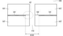
図15は第2の従来技術における第2の基本構成の断面構造を示す断面図である。同図に示す、空隙109が空隙(9)に対応し、第一電極107が一方接地電極(7)に対応し、細孔110が細孔(10)に対応し、接地導電層141が接地導電層(41)に対応し、接地隙間142が接地隙間(42)に対応する。 FIG. 15 is a cross-sectional view showing a cross-sectional structure of a second basic configuration in the second prior art. As shown in the figure, the
同図に示すように、接地導電層141の開口領域H141は細孔110を含み、細孔110より広い形状で形成されているため、電極ユニット100と接地導電層141との間に接地隙間142が生じている。この接地隙間142は、接地導電層141が形成されていない。 As shown in the figure, since the opening region H141 of the ground
したがって、電極間の放電場となる空隙109において、接地隙間142の上方の領域は非放電空間となり、この非放電空間をガスが通過する際には活性ガスが失活するだけとなり、活性ガスの濃度低下を招いてしまう。 Therefore, in the
次に、接地導電層141を改良し、接地隙間142の無い状態(細孔110と本体ポール部の開口領域H141の開口領域とを同じ大きさにする)に変更する変形例を考える。 Next, consider a modified example in which the grounding
図16は、第2の従来技術における第2の基本構成の変形例の断面構造を示す断面図である。図16で示す領域は、図15の着目領域R7及びその近傍領域を拡大して示した領域に相当する。 FIG. 16 is a cross-sectional view showing a cross-sectional structure of a modified example of the second basic configuration in the second prior art. The region shown in FIG. 16 corresponds to the region of interest R7 in FIG. 15 and the region in the vicinity thereof enlarged.
第2の基本構成の変形例では、細孔110を断面方向に観察すると接地導電層141が細孔110に露出した状態となっている。このため、接地導電層141の露出部近傍の細孔110で絶縁破壊が発生した際には、接地導電層141の導電層成分がコンタミとなって外部に放出されることになる。 In the second modification of the basic configuration, when the
このように、第2の従来技術の第2の基本構成(図15)では、活性ガスの濃度低下を招く問題があり、第2の基本構成の変形例(図16)では、コンタミが発生してしまう問題点があった。 As described above, in the second basic configuration (FIG. 15) of the second prior art, there is a problem of causing a decrease in the concentration of the active gas, and in the modified example of the second basic configuration (FIG. 16), contamination occurs. There was a problem that it would end up.
本発明では、上記のような問題点を解決し、装置構成の簡略化及び小型化を図り、かつ、活性ガスが失活する現象を抑制することができる活性ガス生成装置を提供することを目的とする。 It is an object of the present invention to provide an active gas generating apparatus capable of solving the above-mentioned problems, simplifying and downsizing the apparatus configuration, and suppressing the phenomenon of deactivation of the active gas. And.
この発明に係る活性ガス生成装置は、誘電体バリア放電が発生する放電空間に供給された原料ガスを活性化して活性ガスを生成する活性ガス生成装置であって、第1及び第2の電極を有する電極ユニットと、前記電極ユニットに交流電圧を供給する交流電源とを備え、前記電極ユニットは、誘電体で構成される電極本体部と、前記電極本体部内に形成され、各々が導電性を有する前記第1及び第2の電極と、前記電極本体部に形成され、外部から供給される原料ガスを受けるガス吸入口と、前記電極本体部内に形成され、前記ガス吸入口から流入した原料ガスが通過するガス内部流路とを含み、前記ガス内部流路は平面視して螺旋状に設けられ、前記第1及び第2の電極は、前記電極本体部の一部及び前記ガス内部流路を挟んで互いに対向するように、前記ガス内部流路の両側面側に配置され、前記ガス内部流路と共に平面視して螺旋状に設けられ、前記第1及び第2の電極間における前記ガス内部流路内の領域が前記放電空間となり、前記交流電源から前記交流電圧を印加することにより前記放電空間に誘電体バリア放電が発生され、前記電極ユニットは、前記放電空間の下方に前記ガス内部流路に連通して設けられる複数のガス噴出口をさらに含み、前記複数のガス噴出口は1つの前記ガス内部流路に対応して設けられ、前記放電空間に供給された原料ガスを活性化して得られる活性ガスが、前記複数のガス噴出口から噴出される。The active gas generator according to the present invention is an active gas generator that activates a raw material gas supplied to a discharge space where a dielectric barrier discharge is generated to generate an active gas, and has first and second electrodes. The electrode unit includes an electrode unit and an AC power supply that supplies an AC voltage to the electrode unit. The electrode unit is formed in an electrode main body portion made of a dielectric and in the electrode main body portion, each of which has conductivity. The first and second electrodes, a gas suction port formed in the electrode main body and receiving a raw material gas supplied from the outside, and a raw material gas formed in the electrode main body and flowing in from the gas suction port are formed. The gas internal flow path includes a gas internal flow path through which the gas passes, and the gas internal flow path is provided in a spiral shape in a plan view. It is arranged on both side surfaces of the gas internal flow path so as to be sandwiched and opposed to each other, and is provided in a spiral shape in a plan view together with the gas internal flow path, and the inside of the gas between the first and second electrodes. A region in the flow path becomes the discharge space, and by applying the AC voltage from the AC power supply, a dielectric barrier discharge is generated in the discharge space, and the electrode unit has the gas internal flow below the discharge space. Further including a plurality of gas outlets provided in communication with thepath, the plurality of gas outlets are provided corresponding to one gas internal flow path, and activate the raw material gas supplied to the discharge space. The obtained active gas is ejected from the plurality of gas outlets.
請求項1記載の本願発明である活性ガス生成装置の電極ユニットは、平面視して螺旋状に設けられるガス内部流路と、放電空間の下方にガス内部流路に連通して設けられる少なくとも一つのガス噴出口とを含んでいる。 The electrode unit of the active gas generator according to the first aspect of the present invention is provided at least one in communication with a gas internal flow path provided in a spiral shape in a plan view and a gas internal flow path below the discharge space. Includes two gas outlets.
したがって、請求項1記載の本願発明である活性ガス生成装置は、少なくとも一つのガス噴出口と放電空間との間に、誘電体バリア放電に関与しない非放電空間が形成されないため、活性ガスが失活する現象を効果的に抑制する効果を奏する。 Therefore, in the active gas generator according to the present invention according to
さらに、電極本体部にガス吸入口、少なくとも一つのガス噴出口、第1及び第2の電極並びにガス内部流路を設けるという比較的簡単な構成で電極ユニットを得ることができるため、活性ガス生成装置の装置構成の簡略化を図ることができる。 Further, since the electrode unit can be obtained with a relatively simple configuration in which a gas suction port, at least one gas outlet, first and second electrodes, and a gas internal flow path are provided in the electrode main body, an active gas is generated. It is possible to simplify the device configuration of the device.
加えて、請求項1記載の本願発明において、ガス内部流路は平面視して螺旋状に設けられるため、電極ユニット自体の面積を大きくすることなく、少なくとも一つのガス噴出口からガス濃度が飽和した状態で活性ガスを噴出することができるため、装置の小型化を図ることができる。 In addition, in the present invention according to
この発明の目的、特徴、局面、および利点は、以下の詳細な説明と添付図面とによって、より明白となる。 The objects, features, aspects, and advantages of the present invention will be made clearer by the following detailed description and accompanying drawings.
<実施の形態1>
実施の形態1の活性ガス生成装置10は、誘電体バリア放電を行うための電極ユニット100を内部に収納している。<
The
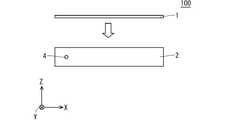
図1は実施の形態1の活性ガス生成装置10に用いられる電極ユニット100の構成概略を示す説明図である。図1にXYZ直交座標系を示している。以下に示す図2~図14においても、図1と同様に、XYZ直交座標系を示している。FIG. 1 is an explanatory diagram showing an outline of the configuration of an
同図に示すように、電極ユニット100は、各々が誘電体で構成される電極ユニット蓋1及び電極ユニットベース2を主要構成部として有している。電極ユニット蓋1は電極ユニットベース2の上面上に設けられ、電極ユニットベース2の側面に原料ガス供給用のガス吸入口4が設けられる。電極ユニット蓋1及び電極ユニットベース2の組合せ構造が電極本体部となる。 As shown in the figure, the
図2は電極ユニットベース2を上方から視た平面構造を示す平面図である。同図に示すように、電極ユニットベース2にはガス通過溝24、高圧電極用溝21、及び接地電極用溝22がそれぞれ電極ユニットベース2の表面から掘られている。ガス通過溝24、高圧電極用溝21及び接地電極用溝22は平面視して螺旋状に形成される。 FIG. 2 is a plan view showing a plan structure of the
図3は電極ユニットベース2の断面構造を示す断面図である。図2のA-A断面が図3となる。 FIG. 3 is a cross-sectional view showing a cross-sectional structure of the
同図に示すように、ガス通過溝24、高圧電極用溝21及び接地電極用溝22は、それぞれの底面が電極ユニットベース2の底面より少し高い位置になるように掘られている。ガス通過溝24、高圧電極用溝21及び接地電極用溝22の表面からの形成深さは同一の深さD2に設定されている。 As shown in the figure, the
このように、電極ユニットベース2は、表面から同一の形成深さで設けられる第1及び第2の電極用溝である高圧電極用溝21及び接地電極用溝22を有している。 As described above, the
さらに、電極ユニットベース2は、表面から深さD2(所定の形成深さ)で溝状に形成されるガス通過溝24を有している。 Further, the
高圧電極用溝21及び接地電極用溝22は、電極ユニットベース2の一部及びガス通過溝24を挟んで互いに対向するように、電極ユニットベース2内のガス通過溝24の両側面側に配置され、ガス通過溝24と共に平面視して螺旋状に設けられる。 The high-
そして、第1の電極である高圧電極11が高圧電極用溝21に埋め込まれ、第2の電極である接地電極12が接地電極用溝22に埋め込まれている。この際、高圧電極11は、高圧電極用溝21に隙間が生じることなく高圧電極用溝21の全体に亘って埋め込まれ、接地電極12は接地電極用溝22に隙間が生じることなく接地電極用溝22の全体に亘って埋め込まれる。 The high-
したがって、高圧電極11及び接地電極12は、電極ユニットベース2の一部及びガス通過溝24を挟んで互いに対向するように、電極ユニットベース2内のガス通過溝24の両側面側に配置され、ガス通過溝24と共に平面視して螺旋状に設けられる。そして、高圧電極11及び接地電極12間におけるガス通過溝24内の領域が放電空間となる。 Therefore, the high-
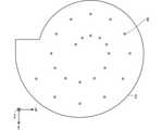
図4は電極ユニットベース2を下方から視た平面構造を示す平面図である。 FIG. 4 is a plan view showing a plan structure of the
図2~図4に示すように、ガス通過溝24の底面下の電極ユニットベース2の領域を貫通する複数のガス噴出口6が互いに離散して選択的に設けられている。複数のガス噴出口6は、放電空間の下方にガス通過溝24の底面に繋がって設けられる。すなわち、複数のガス噴出口6はガス通過溝24に連通している。したがって、ガス通過溝24内で生成された活性ガスを複数のガス噴出口6から外部に噴出することができる。 As shown in FIGS. 2 to 4, a plurality of
また、図1及び図2に示すように、外部から供給される原料ガスを受けるガス吸入口4が電極ユニットベース2の一側面に設けられ、ガス吸入口4に連通してガス通過溝24が設けられる。したがって、ガス通過溝24はガス吸入口4から流入した原料ガスが通過する。 Further, as shown in FIGS. 1 and 2, a
電極ユニット蓋1及び電極ユニットベース2はそれぞれアルミナ等の誘電体で構成される。 The
図5は実施の形態1の活性ガス生成装置10を上方から視た平面構造を模式的に示す平面図である。図6は実施の形態1の活性ガス生成装置10の断面構造を示す断面図である。図5のB-B断面が図6となる。なお、図5では説明の都合上、電極ユニット蓋1が無い状態で示している。 FIG. 5 is a plan view schematically showing a plan structure of the
これらの示すように、電極ユニット100は装置筐体30内に収納されている。装置筐体30はアルミ合金等の金属で形成され、上面に原料ガス供給用のガス供給口34が設けられる。 As shown above, the
装置筐体30は、底面の一部上に電極ユニット100を載置するともに、底面の中央に開口部H30を設けている。開口部H30は平面視して複数のガス噴出口6の全てと重複するように設けられる。 In the
電極ユニット蓋1は電極ユニットベース2の上面上にOリング等のシール部材を介して密着されている。 The
このように、電極ユニットベース2の上面上に電極ユニット蓋1を密着させているため、高圧電極11及び接地電極12は、電極本体部である電極ユニット蓋1及び電極ユニットベース2の組合せ構造から露出することなく、電極本体部内に設けられることになる。 Since the
電極ユニットベース2上に電極ユニット蓋1が密着して設けられているため、電極ユニット100の完成段階では、ガス通過溝24は上部が露出することなく密封されたガス内部流路となる。本明細書では、説明の都合上、電極ユニット蓋1を設ける前の電極ユニットベース2の段階、電極ユニット100の完成段階を含めて「ガス通過溝24」と標記する。 Since the
このような構成の活性ガス生成装置10は、ガス吸入口4から電極ユニット100の内部へと進入したガスは、図5の破線の矢印で示すガスの流れ8に沿って、螺旋状に形成されるガス通過溝24内を進み、ガス通過溝24の底面下に設けられた複数のガス噴出口6から放出される。 In the
図7は実施の形態1の活性ガス生成装置10を用いた成膜処理装置の断面構造を示す断面図である。 FIG. 7 is a cross-sectional view showing a cross-sectional structure of a film forming processing apparatus using the active
同図に示すように、活性ガス生成装置10の直下に成膜処理チャンバ50が配置される。すなわち、活性ガス生成装置10の直下における複数のガス噴出口6から活性ガスが噴出される外部領域が装置下流領域となり、この装置下流領域を含むように成膜処理チャンバ50が配置される。
As shown in the figure, the film forming
成膜処理チャンバ50は上部に開口部58を有し、開口部58は平面視して開口部H30と合致するように設けられる。 The film forming
成膜処理チャンバ50は内部に成膜処理空間60を有し、底面上に設けられた載置テーブル51上に成膜処理対象物であるウェハ55が載置されている。 The film-forming
したがって、活性ガス生成装置10の複数のガス噴出口6から噴出される活性ガスは、開口部H30及び開口部58を介して成膜処理チャンバ50の成膜処理空間60のウェハ55に供給される。すなわち、活性ガス生成装置10から噴出される活性ガスはシャワープレートを介することなくウェハ55に直接供給される。 Therefore, the active gas ejected from the plurality of
そして、成膜処理装置が成膜処理を実行する際、成膜処理チャンバ50の成膜処理空間60の圧力は数kPa以下に、電極ユニット100のガス通過溝24内の圧力は、数kPa~大気圧(=101.33kPa)になるように圧力設定される。 When the film forming processing apparatus executes the film forming process, the pressure in the film forming
複数のガス噴出口6はそれぞれ平面視して微小な直径を有する円状に形成される。このため、複数のガス噴出口6は、ガス通過溝24内と成膜処理チャンバ50の成膜処理空間60内との間に、圧力差を設けるためのオリフィスとして機能することができる。 Each of the plurality of
すなわち、実施の形態1の活性ガス生成装置10において、複数のガス噴出口6は、ガス通過溝24内の圧力が上記装置下流領域を含むように配置された成膜処理空間60内の圧力より高くなるように、比較的小さい寸法で形成される。 That is, in the active
このように、複数のガス噴出口6を比較的小さい寸法で形成して、ガスの流路を絞っている。したがって、ガス通過溝24内に満遍なく活性ガスが充満し、ガス通過溝24及び成膜処理チャンバ50間の圧力差に応じて、複数のガス噴出口6それぞれから均等に活性ガスを噴出することができる。 In this way, the plurality of
このように、実施の形態1の活性ガス生成装置10は、複数のガス噴出口6をオリフィスとして機能させることにより、ガス通過溝24内の圧力が装置下流領域を含む領域に存在する成膜処理空間60の圧力より高くなるように設定している。 As described above, in the active
このため、ガス通過溝24及び成膜処理空間60(成膜処理チャンバ50)間の圧力差に応じて、複数のガス噴出口6それぞれから均等に活性ガスを噴出することができる効果を奏する。 Therefore, the active gas can be evenly ejected from each of the plurality of
活性ガス生成装置10において、ガス通過溝24内の圧力は10kPa~大気圧の間に設定され、成膜処理空間60圧力はガス通過溝24内の圧力未満に設定されることが望ましい。 In the
活性ガス生成装置10は、ガス通過溝24内の圧力を10kPa~大気圧の間(10kPa以上、大気圧以下)に設定することにより、ガス内部流路であるガス通過溝24内に形成される放電空間の圧力を適切に設定することができる。 The
成膜処理チャンバ50は、成膜処理空間60内の圧力をガス通過溝24内の圧力未満に設定することにより、活性ガス生成装置10のガス通過溝24内に活性ガスが充満した状態で、複数のガス噴出口6から活性ガスが噴出される。 By setting the pressure in the film forming
したがって、活性ガス生成装置10は、複数のガス噴出口6間で噴出速度が均等になるように、複数のガス噴出口から活性ガスを噴出することができる。 Therefore, the
その結果、実施の形態1の活性ガス生成装置10と成膜処理チャンバ50とにより構成される上記成膜処理装置は、精度良く成膜処理を行うことができる。 As a result, the film forming processing apparatus including the active
また、電極ユニットベース2の側面に設けたガス吸入口4に関し、活性ガス生成装置10内で特別な配管接続等を必要としない。単に、ガス吸入口4を介して活性ガス生成装置10にガスを供給さえすれば、ガス吸入口4からガス通過溝24の内部にかけて、充満したガスが自然に流れていくという非常にシンプルな構成となっている。 Further, regarding the
なお、電極ユニット100の底面と装置筐体30の底面との間にはOリング等のシール部材を用いて密着されており、活性ガス生成装置10内のガスは、ガス吸入口4、ガス通過溝24及び複数のガス噴出口6よりなるガス流通経路以外に外部への放出経路を有しない。 The bottom surface of the
図2及び図3に示すように、電極ユニットベース2内に掘られた高圧電極用溝21及び接地電極用溝22は、ガス通過溝24と比較して、その形成幅(X方向の長さ)が相当狭い溝となっている。 As shown in FIGS. 2 and 3, the high-
高圧電極11及び接地電極12の形成方法として、高圧電極用溝21内に金属箔や金属板を挿入することにより高圧電極11を構成し、接地電極用溝22内に金属箔や金属板を挿入することにより接地電極12を構成する第1の方法が考えられる。 As a method for forming the high-
しかしながら、金属箔や金属板では溝21及び22との間に隙間が生じやすく、その隙間に高電界強度領域が発生すると容易に絶縁破壊が生じてしまう。このため、高圧電極用溝21及び接地電極用溝22を隙間なく完全に密閉するように、溝21及び22内に金属ペースト等を流し込んで高圧電極11及び接地電極12を形成する第2の方法を上記第1の方法に代えて採用することが望ましい。 However, in a metal foil or a metal plate, a gap is likely to occur between the
高圧電極11及び接地電極12は高周波電源である交流電源5が接続される。具体的には、交流電源5から高圧端子P11を介して高圧電極11に高電圧となる交流電圧が印加され、接地電極12は接地端子P12を介して接地レベルに設定される。 An
図8は電極ユニットベース2を上方から視た平面構造を示す平面図であり、図9は図8の着目領域R2を拡大して示す説明図である。 FIG. 8 is a plan view showing a plan structure when the
図10は電極ユニット100の断面構造を示す断面図であり、図11は図10の着目領域R100を拡大して示す説明図である。 FIG. 10 is a cross-sectional view showing a cross-sectional structure of the
電極ユニットベース2自体は誘電体で構成されるため、交流電源5から10kHz~100kHz、V0p(0ピーク値):2~10kVの交流電圧を印加することにより、高圧電極11及び接地電極12で挟まれたガス通過溝24内の領域である放電空間に誘電体バリア放電16を発生させることができる。 Since the
ガス吸入口4から電極ユニットベース2の内部のガス通過溝24へと進入した原料ガスは、ガス通過溝24内の放電空間を通過しながら、螺旋状のガス通過溝24を中心方向へと進むことで活性化され活性ガスが生成される。 The raw material gas that has entered the
図7に示すように、成膜処理装置における活性ガス生成装置10は、成膜処理チャンバ50の成膜処理空間60内のウェハ55の直上に設置されているため、電極ユニット100内で生成された活性ガスが複数のガス噴出口6を経由してウェハ55に向けて噴出される。 As shown in FIG. 7, since the active
このように、実施の形態1の活性ガス生成装置10を用いた成膜処理装置は、装置下流領域を含む領域に設けられ、複数のガス噴出口6から活性ガスを直接受ける成膜処理空間60を有する成膜処理チャンバ50を備えている。 As described above, the film forming processing apparatus using the active
上記構成の成膜処理装置は、活性ガス生成装置10より生成される活性ガスが比較的寿命の短い活性ガスであっても、活性ガスの減衰を最小限に抑えることができるため、成膜処理空間60内における成膜速度の向上を図ることができる。 In the film forming processing apparatus having the above configuration, even if the active gas generated by the active
また、上述したように、電極本体部を構成する電極ユニット蓋1及び電極ユニットベース2はそれぞれアルミナ等の誘電体で構成される。このため、ガス通過溝24内に形成される放電空間に誘電体バリア放電を生じさせることができる。 Further, as described above, the
なお、電極本体部の構成材料となり得る誘電体として、アルミナ以外に例えば、石英、窒化ケイ素、窒化アルミ、及び窒化ホウ素が考えられる。したがって、電極本体部は、アルミナ、石英、窒化ケイ素、窒化アルミ、及び窒化ホウ素のうち少なくとも一つを構成材料とすれば良い。 As the dielectric that can be a constituent material of the electrode main body, for example, quartz, silicon nitride, aluminum nitride, and boron nitride can be considered in addition to alumina. Therefore, the electrode main body may be made of at least one of alumina, quartz, silicon nitride, aluminum nitride, and boron nitride as a constituent material.
さらに、原料ガスとして、窒素や酸素、希ガス類や水素、弗素類等を用いることでウェハ55に対する様々な処理に使用することが可能となる。 Further, by using nitrogen, oxygen, rare gases, hydrogen, fluorine and the like as the raw material gas, it can be used for various treatments on the
原料ガスは、窒素、酸素、弗素、及び水素のうち少なくとも一つを含むガスであれば以下の効果を発揮することができる。 The raw material gas can exhibit the following effects as long as it is a gas containing at least one of nitrogen, oxygen, fluorine, and hydrogen.
以下、この点を詳述する。窒素や酸素を原料ガスとすれば窒化膜や酸化膜の絶縁膜を成膜することができる。弗素や塩素ガスを原料ガスとすれば、活性化した弗化ガスや塩素ガスをエッチングガスや洗浄ガスとして利用することができる。水素や窒素を原料ガスとすれば、活性化した水素ガスや窒化ガスによってウェハ55等の処理対象物の表面を水素化、窒化して表面改質処理が行える。 This point will be described in detail below. If nitrogen or oxygen is used as the raw material gas, an insulating film of a nitride film or an oxide film can be formed. If fluorine or chlorine gas is used as a raw material gas, the activated fluorine gas or chlorine gas can be used as an etching gas or a cleaning gas. If hydrogen or nitrogen is used as the raw material gas, the surface of the object to be processed such as the
オリフィスとなるガス噴出口6にできるだけ近い領域まで放電場(放電空間)とすることが望ましい。なぜなら、放電場~オリフィス間の経路に放電に関与しない非放電空間が存在すると、非放電空間では活性ガスが生成されずに失活するだけのデッドスペースとなってしまうからである。 It is desirable to set the discharge field (discharge space) as close as possible to the
複数のガス噴出口6の上流に位置するガス通過溝24内は高圧領域であるため、活性ガス失活速度が特に高い。このため、放電場~オリフィス間の経路にわずかな非放電空間が存在しても活性ガス濃度の著しい低下を招いてしまう。 Since the inside of the
前述したように、特許文献2で開示された第2の従来技術の第2の基本構成は、接地隙間142の上方に存在する空隙109に非放電空間が必ず存在する構造(図15参照)であるため、非放電空間での活性ガスの失活は避けられない。 As described above, the second basic configuration of the second prior art disclosed in
さらに、第2の基本構成の変形例では、細孔110に端部が露出した接地導電層141のコンタミ混入の問題点が生じてしまう(図16参照)。 Further, in the second modification of the basic configuration, there arises a problem of contamination contamination of the ground
一方、実施の形態1の活性ガス生成装置10では、図11に示すように、オリフィスである複数のガス噴出口6それぞれの入口まで、放電16が発生する放電場(放電空間)が形成されており、放電場~ガス噴出口6に至る経路における活性ガスの流れ18にデッドスペースとなる非放電空間は存在しない。 On the other hand, in the
このように、実施の形態1の活性ガス生成装置10における電極ユニット100は、平面視して螺旋状に設けられるガス内部流路であるガス通過溝24と、放電空間の下方にガス通過溝24に連通して設けられる複数のガス噴出口6とを含んでいる。 As described above, the
したがって、実施の形態1の活性ガス生成装置10は、複数のガス噴出口6と放電空間との間に、誘電体バリア放電に関与しない非放電空間が形成されないため、活性ガスが失活する現象を効果的に抑制する効果を奏する。 Therefore, in the
なお、上記効果は、ガス噴出口6が一つの場合でも発揮することができる。したがって、上記効果に関し、活性ガス生成装置10は、少なくとも一つのガス噴出口6を設ければ良い。 The above effect can be exhibited even when there is only one
さらに、電極ユニット蓋1及び電極ユニットベース2の組合せ構造である電極本体部にガス吸入口4、複数のガス噴出口6、高圧電極11、接地電極12及びガス通過溝24を設けるという比較的簡単な構成で電極ユニット100を得ることができるため、活性ガス生成装置10の装置構成の簡略化を図ることができる。 Further, it is relatively simple to provide a
加えて、電極ユニットベース2内において、高圧電極11は高圧電極用溝21内に埋め込まれ、接地電極12は接地電極用溝22内に埋め込まれ、かつ、電極ユニットベース2の上面上に電極ユニット蓋1が密着して設けられている。 In addition, in the
したがって、電極ユニット100の高圧電極11及び接地電極12は、活性ガスが流れるガス内部流路であるガス通過溝24や複数のガス噴出口6に繋がるガス流路が存在しないため、仮に高圧電極11及び接地電極12に異常放電が発生しても、ガス通過溝24やガス噴出口6にコンタミが混入する問題は基本的に生じない。 Therefore, since the high-
このように、活性ガス生成装置10の高圧電極11及び接地電極12は、電極ユニット蓋1及び電極ユニットベース2の組合せ構造である電極本体部から露出することなく、ガス通過溝24内に形成される放電空間とは完全分離されて形成されている。 As described above, the high-
このため、実施の形態1の活性ガス生成装置10は、高圧電極11及び接地電極12のいずれかに異常放電が発生しても、異常放電を原因として生じるコンタミが放電空間に混入する問題を確実に回避することができる。 Therefore, the
放電場となるガス通過溝24に進入した原料ガスは、ガス通過溝24内において活性ガスの生成と消滅(失活)とを繰り返す。一定時間以上の放電場滞在時間を設けると、活性ガスの生成量と失活量とが釣り合うために活性ガスが一定濃度となる。これが活性ガス濃度の飽和である。 The raw material gas that has entered the
ウェハ55に対し成膜処理を行う際には処理時間等の都合により活性ガス濃度は高い方が好ましく、複数のガス噴出口6から噴出される活性ガス濃度が全て飽和に達していることは、処理時間のみならず活性ガス濃度の均等化の観点からも望ましい。 When the film formation process is performed on the
特許文献2で開示された第2の従来技術では原料ガスは円盤状電極の外周から内部へと進むものとなっている。この場合、最も放電場滞在時間が短いのが最外周にある細孔(以下、「最外周細孔」と略記する)を介して外部へと放出されるガスの流れとなる。 In the second prior art disclosed in
円盤状電極の外周から最外周細孔に至る最短ガス流路を通過して発生する活性ガスにおいても、活性ガス濃度が全て飽和に達している飽和活性ガスとするためには、最外周細孔と円盤状電極の外周部との距離を飽和ガス形成距離に設定する必要がある。なお、飽和ガス形成距離は、活性ガス濃度が飽和状態となるために必要な距離である。 Even in the active gas generated by passing through the shortest gas flow path from the outer periphery of the disk-shaped electrode to the outermost pore, in order to obtain a saturated active gas in which the active gas concentration has reached saturation, the outermost pore. It is necessary to set the distance between the and the outer peripheral portion of the disk-shaped electrode as the saturated gas formation distance. The saturated gas formation distance is a distance required for the active gas concentration to become saturated.
この場合、円盤状電極の外周から飽和ガス形成距離に至るまで細孔を設けることができないため、複数の細孔を設ける領域である細孔分布領域と比較して相当大きな面積の円盤状電極を設ける必要がある。 In this case, since pores cannot be provided from the outer periphery of the disk-shaped electrode to the saturated gas formation distance, a disk-shaped electrode having a considerably larger area than the pore distribution region, which is a region where a plurality of pores are provided, is provided. Need to be provided.
細孔分布領域は処理対象物となるウェハのサイズで決定される。したがって、例えば、直径300mmのウェハを処理する場合、中心から少なくとも直径300mm程度の領域に最外周細孔を配置する必要が生じる。 The pore distribution region is determined by the size of the wafer to be processed. Therefore, for example, when processing a wafer having a diameter of 300 mm, it is necessary to arrange the outermost pores in a region having a diameter of at least 300 mm from the center.
したがって、細孔分布領域の最外周細孔から径方向に上記飽和ガス形成距離分、さらに延ばした位置が外周となる円盤状電極を設ける必要があり、処理対象物となるウェハと比較して非常に大きな面積の円盤状電極を設ける必要が生じる。 Therefore, it is necessary to provide a disk-shaped electrode whose outer circumference is the saturated gas formation distance in the radial direction from the outermost pore of the pore distribution region, and the extended position is the outer circumference, which is much higher than that of the wafer to be processed. It will be necessary to provide a disk-shaped electrode with a large area.
一方、実施の形態1の活性ガス生成装置10では、螺旋状のガス内部流路となるガス通過溝24は1つ設ければ十分なため、ガス通過溝24における放電空間の形成長を長くしても、電極ユニット100の形成面積はそれほど大きな増大に繋がらない。 On the other hand, in the active
図9に示すように、ガスの流れ18に沿って、原料ガスがガス通過溝24内の放電空間に進入してから最初のガス噴出口6Sに達するまでの領域が、活性ガス濃度増加ゾーンZ24となる。活性ガス濃度増加ゾーンZ24におけるガスの流れ18に沿って、放電空間の入口から最初のガス噴出口6Sに至る螺旋状の距離が第1の活性ガス生成距離となる。この第1の活性ガス生成距離が上記飽和ガス形成距離を満足するように設定すれば、最初のガス噴出口6S以降に設けられるガス噴出口6においてもガス濃度が飽和した状態で活性ガスを噴出させることができる。 As shown in FIG. 9, the region from the entry of the raw material gas into the discharge space in the
以下、活性ガス濃度増加ゾーンZ24内の第1の活性ガス生成距離の具体例を示す。例えば、ガス通過溝24の形成幅(X方向の長さ)が3mm、ガス通過溝24の形成高さ(Z方向の長さ)が50mmの場合を考える。なお、高圧電極用溝21及び接地電極用溝22もガス通過溝24と同じ深さD2で形成されているため、高圧電極11及び接地電極12の形成高さも50mmとなる。 Hereinafter, a specific example of the first active gas generation distance in the active gas concentration increase zone Z24 will be shown. For example, consider a case where the formation width (length in the X direction) of the
この際、ガス通過溝24内の圧力を30kPaに設定し、ガス吸入口4から供給する原料ガスのガス流量:10slmとすると、第1の活性ガス生成距離を70mm以上に設定すれば良い。すなわち、上記飽和ガス形成距離は70mmとなる。 At this time, if the pressure in the
上述したように、実施の形態1の活性ガス生成装置10内において、放電空間を形成するガス通過溝24は平面視して螺旋状に設けられるため、電極ユニット100自体の面積をさほど大きくすることなく、複数のガス噴出口6からガス濃度が飽和した状態で活性ガスを噴出することができる。 As described above, in the
その結果、実施の形態1の活性ガス生成装置10は、電極ユニット100の形成面積をウェハ55等の処理対象物と同等な形成面積に抑えることができるため、装置の小型化を図ることができる。 As a result, in the active
また、高圧電極11及び接地電極12は平面視して螺旋状に形成されているため、特許文献2に開示された第2の従来技術と比較した場合、電極面積の増大を著しく抑えることが可能となる。 Further, since the high-
また、実施の形態1の活性ガス生成装置10では、電極ユニット100内において、高圧電極11及び接地電極12に関し、平面視して電極ユニットベース2の最外周に接地電極12が位置するように配置されている。 Further, in the
このため、高電圧が印加される高圧電極11から電極ユニットベース2の外周部に向かう電界ベクトルを、高圧電極11より外周に存在する接地電極12によって必ず吸収することができる。 Therefore, the electric field vector from the high-
したがって、実施の形態1の活性ガス生成装置10は、高圧電極11に起因して外部の装置筐体30に異常放電が発生する可能性を確実に抑制することができる。 Therefore, the active
したがって、実施の形態1の活性ガス生成装置10は、第2の従来技術の第1の基本構成のように、高圧電極を構成する導電層における異常放電に起因して、放電部にパーティクルや金属蒸気が生成し、処理対象物を汚染する恐れはない。さらに、活性ガス生成装置10は装置筐体30内の内部空間は特に絶縁距離を考慮する必要はないため、装置が大型化することもない。 Therefore, the
また、実施の形態1の活性ガス生成装置10は、複数のガス噴出口6は平面視して螺旋状に離散配置される特徴を有している。 Further, the
このため、実施の形態1の活性ガス生成装置10は、複数のガス噴出口6から活性ガスを噴出することより、比較的大きな処理対象物に対しても均等に活性ガスを噴出することができる。 Therefore, the
<実施の形態2>
図12は実施の形態2の活性ガス生成装置10における電極の断面構造を示す断面図である。図13は実施の形態1の活性ガス生成装置10における電極の断面構造を示す断面図である。<
FIG. 12 is a cross-sectional view showing a cross-sectional structure of an electrode in the
図12に示すように、実施の形態2においては、高圧電極用溝21の上方に空間領域が残存するように、高圧電極用溝21内の一部に高圧電極11Lが埋め込まれる。一方、接地電極用溝22内に埋め込まれる接地電極12は、実施の形態1と同様、接地電極用溝22に隙間を設けることなく全体に亘って埋め込まれる。 As shown in FIG. 12, in the second embodiment, the high-
したがって、実施の形態2の活性ガス生成装置10は、高圧電極11Lの形成高さを接地電極12の形成高さに比べ、低く設定していることを特徴としている。 Therefore, the
図13に示すように、高圧電極11及び接地電極12の形成高さが同じである実施の形態1では、高圧電極11の最上部と接地電極12の最上部との間にて異常放電経路96が生成する恐れがある。なぜなら、電極ユニットベース2上に電極ユニット蓋1を密着して設けても、電極ユニットベース2と電極ユニット蓋1との間にわずかな隙間が生じる可能性があるからである。As shown in FIG. 13, in the first embodiment in which the formation heights of the high-
異常放電経路96に異常放電が発生した際、電極ユニット蓋1と電極ユニットベース2との間にわずかでも隙間が生じていた場合、そのわずかな隙間を経由して、高圧電極11あるいは接地電極12の電極成分が汚染物質となってガス内部流路であるガス通過溝24に混入する恐れがある。 When an abnormal discharge occurs in the
一方、実施の形態2の活性ガス生成装置10は、高圧電極11Lの形成高さを接地電極12よりも低くすることにより、高圧電極11Lの最上部と接地電極12の最上部との間における最上部電極間距離を、実施の形態1に比べ長く設定することができる分、異常放電の発生を効果的に抑制することができる。 On the other hand, in the
なお、実施の形態2の活性ガス生成装置10は、高圧電極11が高圧電極11Lに置き換わった点を除き、実施の形態1と同様な構成を呈しているため、実施の形態1と同様な効果を併せて奏する。 The
<実施の形態3>
図14は実施の形態3の活性ガス生成装置10Bの断面構造を示す断面図である。<Embodiment 3>
FIG. 14 is a cross-sectional view showing a cross-sectional structure of the
同図に示すように、活性ガス生成装置10Bは電極ユニット100Bを有している。電極ユニット100Bは、電極ユニット蓋1の上面上に、誘電体で構成される冷却フィン40を設けたことを特徴としている。なお、他の構成は実施の形態1と同様であるため、同一符号を付し、説明を適宜省略する。 As shown in the figure, the
電極ユニットは、放電空間における誘電体バリア放電の発生に伴い熱を生成し、活性ガス生成装置における金属製の装置筐体と誘電体で構成される電極本体部(電極ユニット蓋1+電極ユニットベース2)との間の熱膨張の違いから歪が生じる恐れがある。The electrodeunit generates heat as a dielectric barrier discharge occurs in the discharge space, and the electrode body (
金属製の水冷ユニットで電極ユニットを囲む冷却方法は、水冷ユニットに異常放電が発生する可能性があるため実用には適さない。 The cooling method in which the electrode unit is surrounded by a metal water cooling unit is not suitable for practical use because an abnormal discharge may occur in the water cooling unit.
そこで、実施の形態3の活性ガス生成装置10Bは、セラミックやガラス等の誘電体で構成された冷却フィン40を電極ユニット蓋1の上面上に密着させることにより、電極ユニット100B内の電極ユニットベース2の熱除去を行っている。 Therefore, in the active
したがって、実施の形態3の活性ガス生成装置10Bは、異常放電を発生させることなく、冷却フィン40によって電極ユニット100Bを冷却することができる。Therefore, the
なお、実施の形態3の活性ガス生成装置10Bは、冷却フィン40が追加された点を除き、実施の形態1と同様な構成を呈しているため、実施の形態1と同様な効果を併せて奏する。また、高圧電極11を実施の形態2の高圧電極11L(図12参照)に置き換えることにより、実施の形態2と同様な効果を併せて奏する。 Since the
この発明は詳細に説明されたが、上記した説明は、すべての局面において、例示であって、この発明がそれに限定されるものではない。例示されていない無数の変形例が、この発明の範囲から外れることなく想定され得るものと解される。 Although the invention has been described in detail, the above description is exemplary in all aspects and the invention is not limited thereto. It is understood that innumerable variations not illustrated can be assumed without departing from the scope of the present invention.
1 電極ユニット蓋
2 電極ユニットベース
4 ガス吸入口
6 ガス噴出口
6S 最初のガス噴出口
10 活性ガス生成装置
11,11L 高圧電極
12 接地電極
21 高圧電極用溝
22 接地電極用溝
30 装置筐体
50 成膜処理チャンバ
60 成膜処理空間
100,100B 電極ユニット1
Claims (11)
Translated fromJapanese第1の電極(11,11L)及び第2の電極(12)を有する電極ユニット(100,100B)と、
前記電極ユニットに交流電圧を供給する交流電源(5)とを備え、
前記電極ユニットは、
誘電体で構成される電極本体部(1,2)と、
前記電極本体部内に形成され、各々が導電性を有する前記第1及び第2の電極と、
前記電極本体部に形成され、外部から供給される原料ガスを受けるガス吸入口(4)と、
前記電極本体部内に形成され、前記ガス吸入口から流入した原料ガスが通過するガス内部流路(24)とを含み、前記ガス内部流路は平面視して螺旋状に設けられ、
前記第1及び第2の電極は、前記電極本体部の一部及び前記ガス内部流路を挟んで互いに対向するように、前記ガス内部流路の両側面側に配置され、前記ガス内部流路と共に平面視して螺旋状に設けられ、前記第1及び第2の電極間における前記ガス内部流路内の領域が前記放電空間となり、前記交流電源から前記交流電圧を印加することにより前記放電空間に誘電体バリア放電が発生され、
前記電極ユニットは、前記放電空間の下方に前記ガス内部流路に連通して設けられる複数のガス噴出口(6)をさらに含み、前記複数のガス噴出口は1つの前記ガス内部流路に対応して設けられ、前記放電空間に供給された原料ガスを活性化して得られる活性ガスが、前記複数のガス噴出口から噴出される、
活性ガス生成装置。An active gas generator (10, 10B) that activates a raw material gas supplied to a discharge space where a dielectric barrier discharge is generated to generate an active gas.
An electrode unit (100, 100B) having a first electrode (11, 11L) and a second electrode (12),
It is equipped with an AC power supply (5) that supplies AC voltage to the electrode unit.
The electrode unit is
Electrode body parts (1, 2) made of dielectric and
The first and second electrodes formed in the electrode body and each having conductivity,
A gas suction port (4) formed in the electrode main body and receiving a raw material gas supplied from the outside,
The gas internal flow path (24) formed in the electrode main body and through which the raw material gas flowing in from the gas suction port passes is included, and the gas internal flow path is provided spirally in a plan view.
The first and second electrodes are arranged on both side surfaces of the gas internal flow path so as to face each other with a part of the electrode main body and the gas internal flow path interposed therebetween, and the gas internal flow path is provided. The region in the gas internal flow path between the first and second electrodes is the discharge space, and the discharge space is formed by applying the AC voltage from the AC power source. Dielectric barrier discharge is generated in
The electrode unit further includes a plurality of gas outlets (6) provided below the discharge space so as to communicate with the gas internal flow path, and theplurality of gas outlets correspond to one gas internal flow path. The active gas obtained by activating the raw material gas supplied tothe discharge space is ejected from the plurality of gas outlets.
Inert gas generator.
前記第1及び第2の電極は、前記電極本体部から露出することなく形成される、
活性ガス生成装置。The active gas generator according to claim 1.
The first and second electrodes are formed without being exposed from the electrode body.
Inert gas generator.
前記第2の電極が接地レベルに設定され、前記第1の電極に前記交流電圧が印加され、
前記第1及び第2の電極は、平面視して前記電極本体部の最外周に前記第2の電極が位置するように、配置されることを特徴とする、
活性ガス生成装置。The active gas generator according to claim 1 or 2.
The second electrode is set to the ground level, the AC voltage is applied to the first electrode, and the AC voltage is applied.
The first and second electrodes are arranged so that the second electrode is located on the outermost periphery of the electrode main body in a plan view.
Inert gas generator.
前記電極本体部は、
電極ユニットベース(2)と、
前記電極ユニットベースの表面上に設けられる電極ユニット蓋(1)とを含み、
前記電極ユニットベースは表面から同一の形成深さで設けられる第1及び第2の電極用溝(21,22)を有し、
前記ガス内部流路は、前記電極ユニットベースの表面から所定の形成深さを有して溝状に形成され、
前記第1及び第2の電極は第1及び第2の電極用溝(21,22)に埋め込まれ、
前記第1の電極(11L)の形成高さを前記第2の電極(12)の形成高さよりも低く設定したことを特徴とする、
活性ガス生成装置。The active gas generator according to any one of claims 1 to 3.
The electrode body is
Electrode unit base (2) and
The electrode unit lid (1) provided on the surface of the electrode unit base is included.
The electrode unit base has first and second electrode grooves (21, 22) provided at the same formation depth from the surface.
The gas internal flow path is formed in a groove shape with a predetermined formation depth from the surface of the electrode unit base.
The first and second electrodes are embedded in the grooves (21, 22) for the first and second electrodes.
It is characterized in that the formation height of the first electrode (11L) is set lower than the formation height of the second electrode (12).
Inert gas generator.
前記複数のガス噴出口の直下に位置し、前記複数のガス噴出口から活性ガスが噴出される外部領域が装置下流領域として規定され、前記複数のガス噴出口は、前記ガス内部流路内の圧力が前記装置下流領域の圧力より高くなるように、比較的小さい寸法で形成されることを特徴とする、
活性ガス生成装置。The active gas generator according to any one of claims 1 to 4.
An external region located directly below the plurality of gas outlets and from which the active gas is ejected from the plurality of gas outlets is defined as a downstream region of the apparatus, and the plurality of gas outlets are in the gas internal flow path. It is characterized in that it is formed in a relatively small size so that the pressure is higher than the pressure in the downstream region of the device.
Inert gas generator.
前記複数のガス噴出口は平面視して螺旋状に離散配置されることを特徴とする、
活性ガス生成装置。The active gas generator according to claim 5.
The plurality of gas outlets are discretely arranged in a spiral shape in a plan view.
Inert gas generator.
誘電体で構成され、前記電極ユニットの前記電極本体部に密着して設けられる冷却フィンをさらに備える、
活性ガス生成装置。The active gas generator according to any one of claims 1 to 6.
Further provided with cooling fins made of a dielectric and provided in close contact with theelectrode body of the electrode unit.
Inert gas generator.
前記電極本体部は、アルミナ、石英、窒化ケイ素、窒化アルミ、及び窒化ホウ素のうち少なくとも一つを構成材料としている、
活性ガス生成装置。The active gas generator according to any one of claims 1 to 7.
The electrode body is made of at least one of alumina, quartz, silicon nitride, aluminum nitride, and boron nitride.
Inert gas generator.
前記原料ガスは、窒素、酸素、弗素、及び水素のうち少なくとも一つを含むガスである、
活性ガス生成装置。The active gas generator according to any one of claims 1 to 8.
The raw material gas is a gas containing at least one of nitrogen, oxygen, fluorine, and hydrogen.
Inert gas generator.
前記装置下流領域を含む領域に設けられ、前記複数のガス噴出口から活性ガスを直接受ける成膜処理空間を有する成膜処理チャンバ(50)とを備える、
成膜処理装置。The active gas generator according to claim 6 and
It is provided with a film forming processing chamber (50) provided in a region including the downstream region of the apparatus and having a film forming processing space for directly receiving an active gas from the plurality of gas outlets.
Film formation processing equipment.
前記ガス内部流路内の圧力は10kPa~大気圧の間に設定され、
前記成膜処理空間内の圧力が前記ガス内部流路内の圧力未満に設定される、
成膜処理装置。The film forming processing apparatus according to claim 10.
The pressure in the gas internal flow path is set between 10 kPa and atmospheric pressure.
The pressure in the film forming processing space is set to be less than the pressure in the gas internal flow path.
Film formation processing equipment.
Applications Claiming Priority (1)
| Application Number | Priority Date | Filing Date | Title |
|---|---|---|---|
| PCT/JP2018/023972WO2020003344A1 (en) | 2018-06-25 | 2018-06-25 | Active gas generation device and film formation treatment unit |
Publications (2)
| Publication Number | Publication Date |
|---|---|
| JPWO2020003344A1 JPWO2020003344A1 (en) | 2021-02-15 |
| JP7019276B2true JP7019276B2 (en) | 2022-02-15 |
Family
ID=68986226
Family Applications (1)
| Application Number | Title | Priority Date | Filing Date |
|---|---|---|---|
| JP2020526726AActiveJP7019276B2 (en) | 2018-06-25 | 2018-06-25 | Inert gas generator and film formation processing equipment |
Country Status (6)
| Country | Link |
|---|---|
| US (1) | US11309167B2 (en) |
| JP (1) | JP7019276B2 (en) |
| KR (1) | KR102510329B1 (en) |
| CN (1) | CN112334599B (en) |
| TW (1) | TWI746923B (en) |
| WO (1) | WO2020003344A1 (en) |
Families Citing this family (5)
| Publication number | Priority date | Publication date | Assignee | Title |
|---|---|---|---|---|
| US11881384B2 (en) | 2019-09-27 | 2024-01-23 | Applied Materials, Inc. | Monolithic modular microwave source with integrated process gas distribution |
| CN113170567B (en) | 2019-11-12 | 2023-11-28 | 东芝三菱电机产业系统株式会社 | Active gas generating device |
| CN113179676B (en)* | 2019-11-27 | 2024-04-09 | 东芝三菱电机产业系统株式会社 | Active gas generating device |
| CN117426143A (en)* | 2022-05-18 | 2024-01-19 | 东芝三菱电机产业系统株式会社 | Active gas generating device |
| CN119256626A (en)* | 2023-05-01 | 2025-01-03 | 东芝三菱电机产业系统株式会社 | Active gas generator |
Citations (5)
| Publication number | Priority date | Publication date | Assignee | Title |
|---|---|---|---|---|
| JP2010503962A (en) | 2006-09-14 | 2010-02-04 | シーエムテック カンパニー リミテッド | Plasma reactor |
| JP2011011183A (en) | 2009-07-06 | 2011-01-20 | Toshiba Mitsubishi-Electric Industrial System Corp | Activated gas generator and remote plasma coating device |
| JP2014523771A (en) | 2011-06-23 | 2014-09-18 | シノギー・ゲーエムベーハー | Electrode assembly for dielectric-blocked gas discharge |
| JP2017091709A (en) | 2015-11-06 | 2017-05-25 | エア・ウォーター株式会社 | Ambient air pressure plasma processing apparatus |
| JP2017091708A (en) | 2015-11-06 | 2017-05-25 | エア・ウォーター株式会社 | Ambient pressure plasma processing apparatus |
Family Cites Families (28)
| Publication number | Priority date | Publication date | Assignee | Title |
|---|---|---|---|---|
| JPS5139811A (en) | 1974-09-30 | 1976-04-03 | Senyo Kiko Kk | Norikagokurumanado no futenseigyosochi |
| US4472174A (en)* | 1983-04-25 | 1984-09-18 | Raymond L. Chuan | Method and apparatus for providing and using RF generated plasma for particle charging in electrostatic precipitation |
| US4735633A (en)* | 1987-06-23 | 1988-04-05 | Chiu Kin Chung R | Method and system for vapor extraction from gases |
| JP2537304B2 (en)* | 1989-12-07 | 1996-09-25 | 新技術事業団 | Atmospheric pressure plasma reaction method and apparatus |
| US5525159A (en)* | 1993-12-17 | 1996-06-11 | Tokyo Electron Limited | Plasma process apparatus |
| US5580385A (en)* | 1994-06-30 | 1996-12-03 | Texas Instruments, Incorporated | Structure and method for incorporating an inductively coupled plasma source in a plasma processing chamber |
| US5846883A (en)* | 1996-07-10 | 1998-12-08 | Cvc, Inc. | Method for multi-zone high-density inductively-coupled plasma generation |
| US6209480B1 (en)* | 1996-07-10 | 2001-04-03 | Mehrdad M. Moslehi | Hermetically-sealed inductively-coupled plasma source structure and method of use |
| JPH1041286A (en)* | 1996-07-26 | 1998-02-13 | Mitsubishi Heavy Ind Ltd | Plasma cvd apparatus |
| JP4658298B2 (en)* | 2000-09-11 | 2011-03-23 | 中部電力株式会社 | Ozone generator |
| JP4161019B2 (en)* | 2000-10-30 | 2008-10-08 | メタウォーター株式会社 | Ozone generator |
| CN1293608C (en)* | 2002-10-16 | 2007-01-03 | 夏普株式会社 | Semiconductor device and its manufacturing method and plasma processing device |
| CN1323751C (en)* | 2003-05-27 | 2007-07-04 | 松下电工株式会社 | Plasma processing apparatus, manufacturing method of plasma generating reaction vessel, and plasma processing method |
| JP4904202B2 (en)* | 2006-05-22 | 2012-03-28 | ジーイーエヌ カンパニー リミッテッド | Plasma reactor |
| JP2008153147A (en)* | 2006-12-20 | 2008-07-03 | Seiko Epson Corp | Plasma processing equipment |
| JP4826483B2 (en)* | 2007-01-19 | 2011-11-30 | 東京エレクトロン株式会社 | Plasma processing equipment |
| US9157152B2 (en)* | 2007-03-29 | 2015-10-13 | Tokyo Electron Limited | Vapor deposition system |
| US20080314734A1 (en)* | 2007-06-21 | 2008-12-25 | The Regents Of The University Of California | Carbonaceous solid fuel gasifier utilizing dielectric barrier non-thermal plasma |
| KR100979189B1 (en)* | 2007-12-20 | 2010-08-31 | 다이나믹솔라디자인 주식회사 | Continuous substrate processing system |
| JP2009260199A (en)* | 2008-03-28 | 2009-11-05 | Toray Ind Inc | Plasma cvd device, and plasma cvd method |
| JP5423205B2 (en)* | 2008-08-29 | 2014-02-19 | 東京エレクトロン株式会社 | Deposition equipment |
| JP5648349B2 (en)* | 2009-09-17 | 2015-01-07 | 東京エレクトロン株式会社 | Deposition equipment |
| JP5328685B2 (en) | 2010-01-28 | 2013-10-30 | 三菱電機株式会社 | Plasma processing apparatus and plasma processing method |
| TW201309105A (en)* | 2011-04-28 | 2013-02-16 | Asahi Organic Chem Ind | Plasma generating method and generating device |
| US9279185B2 (en)* | 2012-06-14 | 2016-03-08 | Asm Technology Singapore Pte Ltd | Feed-through apparatus for a chemical vapour deposition device |
| US9497846B2 (en)* | 2013-10-24 | 2016-11-15 | The United States Of America As Represented By The Administrator Of The National Aeronautics And Space Administration | Plasma generator using spiral conductors |
| TWI677593B (en)* | 2016-04-01 | 2019-11-21 | 美商應用材料股份有限公司 | Apparatus and method for providing a uniform flow of gas |
| TWI848974B (en)* | 2018-09-14 | 2024-07-21 | 美商應用材料股份有限公司 | Apparatus for multi-flow precursor dosage |
- 2018
- 2018-06-25JPJP2020526726Apatent/JP7019276B2/enactiveActive
- 2018-06-25CNCN201880094582.0Apatent/CN112334599B/enactiveActive
- 2018-06-25KRKR1020207036921Apatent/KR102510329B1/enactiveActive
- 2018-06-25USUS17/050,853patent/US11309167B2/enactiveActive
- 2018-06-25WOPCT/JP2018/023972patent/WO2020003344A1/ennot_activeCeased
- 2019
- 2019-01-10TWTW108101018Apatent/TWI746923B/enactive
Patent Citations (5)
| Publication number | Priority date | Publication date | Assignee | Title |
|---|---|---|---|---|
| JP2010503962A (en) | 2006-09-14 | 2010-02-04 | シーエムテック カンパニー リミテッド | Plasma reactor |
| JP2011011183A (en) | 2009-07-06 | 2011-01-20 | Toshiba Mitsubishi-Electric Industrial System Corp | Activated gas generator and remote plasma coating device |
| JP2014523771A (en) | 2011-06-23 | 2014-09-18 | シノギー・ゲーエムベーハー | Electrode assembly for dielectric-blocked gas discharge |
| JP2017091709A (en) | 2015-11-06 | 2017-05-25 | エア・ウォーター株式会社 | Ambient air pressure plasma processing apparatus |
| JP2017091708A (en) | 2015-11-06 | 2017-05-25 | エア・ウォーター株式会社 | Ambient pressure plasma processing apparatus |
Also Published As
| Publication number | Publication date |
|---|---|
| TW202001984A (en) | 2020-01-01 |
| WO2020003344A1 (en) | 2020-01-02 |
| KR102510329B1 (en) | 2023-03-17 |
| TWI746923B (en) | 2021-11-21 |
| CN112334599A (en) | 2021-02-05 |
| KR20210011444A (en) | 2021-02-01 |
| CN112334599B (en) | 2023-09-29 |
| US11309167B2 (en) | 2022-04-19 |
| US20210233748A1 (en) | 2021-07-29 |
| JPWO2020003344A1 (en) | 2021-02-15 |
Similar Documents
| Publication | Publication Date | Title |
|---|---|---|
| JP7019276B2 (en) | Inert gas generator and film formation processing equipment | |
| JP5328685B2 (en) | Plasma processing apparatus and plasma processing method | |
| CN100524641C (en) | Plasma processing device | |
| CN105719932B (en) | Double plasma volume processing unit for neutral particle/ion flux control | |
| KR101913978B1 (en) | Radical gas generation system | |
| TWM574753U (en) | Semiconductor processing system | |
| JP5694542B2 (en) | Plasma generator and CVD apparatus | |
| TW201833373A (en) | Substrate processing equipment | |
| JP5025614B2 (en) | Atmospheric pressure plasma treatment method | |
| CN104981895A (en) | Semiconductor processing systems having multiple plasma configurations | |
| JP6844937B2 (en) | Inert gas generator | |
| JP6339218B2 (en) | Gas injection device for film forming equipment | |
| KR20190130044A (en) | High deposition rate, high quality silicon nitride made possible by remote nitrogen radical source | |
| TW201615283A (en) | Gas injection device | |
| JP7133454B2 (en) | Plasma processing equipment | |
| JP2011011183A (en) | Activated gas generator and remote plasma coating device | |
| TW201724165A (en) | Plasma photoresist etching device capable of maintaining photoresist etching rate of a substrate at a higher level | |
| JP2013004474A (en) | Plasma generator and cvd device | |
| JP5613641B2 (en) | Plasma generator and CVD apparatus | |
| JP2017045671A (en) | Plasma processing apparatus and plasma processing method | |
| JP2010123812A (en) | Plasma processing device and plasma processing method | |
| JP2004134680A (en) | Oxidized film forming method and apparatus thereof | |
| JP2010153528A (en) | Substrate processing equipment |
Legal Events
| Date | Code | Title | Description |
|---|---|---|---|
| A521 | Request for written amendment filed | Free format text:JAPANESE INTERMEDIATE CODE: A523 Effective date:20200715 | |
| A621 | Written request for application examination | Free format text:JAPANESE INTERMEDIATE CODE: A621 Effective date:20200715 | |
| A131 | Notification of reasons for refusal | Free format text:JAPANESE INTERMEDIATE CODE: A131 Effective date:20210824 | |
| A521 | Request for written amendment filed | Free format text:JAPANESE INTERMEDIATE CODE: A523 Effective date:20210928 | |
| TRDD | Decision of grant or rejection written | ||
| A01 | Written decision to grant a patent or to grant a registration (utility model) | Free format text:JAPANESE INTERMEDIATE CODE: A01 Effective date:20220201 | |
| A61 | First payment of annual fees (during grant procedure) | Free format text:JAPANESE INTERMEDIATE CODE: A61 Effective date:20220201 | |
| R150 | Certificate of patent or registration of utility model | Ref document number:7019276 Country of ref document:JP Free format text:JAPANESE INTERMEDIATE CODE: R150 | |
| R250 | Receipt of annual fees | Free format text:JAPANESE INTERMEDIATE CODE: R250 |