JP7010668B2 - Semiconductor device - Google Patents
Semiconductor deviceDownload PDFInfo
- Publication number
- JP7010668B2 JP7010668B2JP2017215445AJP2017215445AJP7010668B2JP 7010668 B2JP7010668 B2JP 7010668B2JP 2017215445 AJP2017215445 AJP 2017215445AJP 2017215445 AJP2017215445 AJP 2017215445AJP 7010668 B2JP7010668 B2JP 7010668B2
- Authority
- JP
- Japan
- Prior art keywords
- metal film
- semiconductor device
- polycrystalline silicon
- resistance circuit
- circuit element
- Prior art date
- Legal status (The legal status is an assumption and is not a legal conclusion. Google has not performed a legal analysis and makes no representation as to the accuracy of the status listed.)
- Active
Links
Images


Classifications
- H—ELECTRICITY
- H10—SEMICONDUCTOR DEVICES; ELECTRIC SOLID-STATE DEVICES NOT OTHERWISE PROVIDED FOR
- H10D—INORGANIC ELECTRIC SEMICONDUCTOR DEVICES
- H10D84/00—Integrated devices formed in or on semiconductor substrates that comprise only semiconducting layers, e.g. on Si wafers or on GaAs-on-Si wafers
- H10D84/201—Integrated devices formed in or on semiconductor substrates that comprise only semiconducting layers, e.g. on Si wafers or on GaAs-on-Si wafers characterised by the integration of only components covered by H10D1/00 or H10D8/00, e.g. RLC circuits
- H10D84/204—Integrated devices formed in or on semiconductor substrates that comprise only semiconducting layers, e.g. on Si wafers or on GaAs-on-Si wafers characterised by the integration of only components covered by H10D1/00 or H10D8/00, e.g. RLC circuits of combinations of diodes or capacitors or resistors
- H10D84/209—Integrated devices formed in or on semiconductor substrates that comprise only semiconducting layers, e.g. on Si wafers or on GaAs-on-Si wafers characterised by the integration of only components covered by H10D1/00 or H10D8/00, e.g. RLC circuits of combinations of diodes or capacitors or resistors of only resistors
- H—ELECTRICITY
- H01—ELECTRIC ELEMENTS
- H01L—SEMICONDUCTOR DEVICES NOT COVERED BY CLASS H10
- H01L21/00—Processes or apparatus adapted for the manufacture or treatment of semiconductor or solid state devices or of parts thereof
- H01L21/02—Manufacture or treatment of semiconductor devices or of parts thereof
- H01L21/02104—Forming layers
- H01L21/02107—Forming insulating materials on a substrate
- H01L21/02109—Forming insulating materials on a substrate characterised by the type of layer, e.g. type of material, porous/non-porous, pre-cursors, mixtures or laminates
- H01L21/02112—Forming insulating materials on a substrate characterised by the type of layer, e.g. type of material, porous/non-porous, pre-cursors, mixtures or laminates characterised by the material of the layer
- H01L21/02123—Forming insulating materials on a substrate characterised by the type of layer, e.g. type of material, porous/non-porous, pre-cursors, mixtures or laminates characterised by the material of the layer the material containing silicon
- H01L21/0217—Forming insulating materials on a substrate characterised by the type of layer, e.g. type of material, porous/non-porous, pre-cursors, mixtures or laminates characterised by the material of the layer the material containing silicon the material being a silicon nitride not containing oxygen, e.g. SixNy or SixByNz
- H—ELECTRICITY
- H01—ELECTRIC ELEMENTS
- H01L—SEMICONDUCTOR DEVICES NOT COVERED BY CLASS H10
- H01L21/00—Processes or apparatus adapted for the manufacture or treatment of semiconductor or solid state devices or of parts thereof
- H01L21/02—Manufacture or treatment of semiconductor devices or of parts thereof
- H01L21/02104—Forming layers
- H01L21/02365—Forming inorganic semiconducting materials on a substrate
- H01L21/02518—Deposited layers
- H01L21/02521—Materials
- H01L21/02538—Group 13/15 materials
- H01L21/0254—Nitrides
- H—ELECTRICITY
- H01—ELECTRIC ELEMENTS
- H01L—SEMICONDUCTOR DEVICES NOT COVERED BY CLASS H10
- H01L21/00—Processes or apparatus adapted for the manufacture or treatment of semiconductor or solid state devices or of parts thereof
- H01L21/70—Manufacture or treatment of devices consisting of a plurality of solid state components formed in or on a common substrate or of parts thereof; Manufacture of integrated circuit devices or of parts thereof
- H01L21/71—Manufacture of specific parts of devices defined in group H01L21/70
- H01L21/768—Applying interconnections to be used for carrying current between separate components within a device comprising conductors and dielectrics
- H01L21/76838—Applying interconnections to be used for carrying current between separate components within a device comprising conductors and dielectrics characterised by the formation and the after-treatment of the conductors
- H—ELECTRICITY
- H10—SEMICONDUCTOR DEVICES; ELECTRIC SOLID-STATE DEVICES NOT OTHERWISE PROVIDED FOR
- H10D—INORGANIC ELECTRIC SEMICONDUCTOR DEVICES
- H10D84/00—Integrated devices formed in or on semiconductor substrates that comprise only semiconducting layers, e.g. on Si wafers or on GaAs-on-Si wafers
Landscapes
- Engineering & Computer Science (AREA)
- Microelectronics & Electronic Packaging (AREA)
- Condensed Matter Physics & Semiconductors (AREA)
- General Physics & Mathematics (AREA)
- Manufacturing & Machinery (AREA)
- Computer Hardware Design (AREA)
- Physics & Mathematics (AREA)
- Power Engineering (AREA)
- Semiconductor Integrated Circuits (AREA)
- Internal Circuitry In Semiconductor Integrated Circuit Devices (AREA)
- Mechanical Treatment Of Semiconductor (AREA)
- Bipolar Transistors (AREA)
- Noodles (AREA)
Description
Translated fromJapanese本発明は、半導体装置に関する。 The present invention relates to a semiconductor device.
検出電圧器等のアナログICは、トランジスタと抵抗体を組み合わせて所望の特性を出力するように、例えば多結晶シリコンの薄膜抵抗体で構成されたブリーダー抵抗回路を備え、その抵抗分圧比が調整されている。この薄膜抵抗体上には、層間絶縁膜および最終保護膜が形成されるが、その形成過程において拡散する水素の浸入により、ブリーダー抵抗回路の抵抗分圧比がウェハ面内でバラつき、歩留りが低下してしまう問題が知られている。一般的な半導体装置は、薄膜抵抗体上に大面積の金属配線を切れ目なく配置し、この水素浸入の問題を回避している。 An analog IC such as a detection voltage device is provided with a bleeder resistance circuit composed of, for example, a thin film resistor made of polycrystalline silicon so as to output desired characteristics by combining a transistor and a resistor, and its resistance voltage division ratio is adjusted. ing. An interlayer insulating film and a final protective film are formed on this thin film resistor, but the resistance voltage division ratio of the bleeder resistance circuit varies in the wafer surface due to the infiltration of hydrogen diffused during the formation process, and the yield decreases. The problem is known. In a general semiconductor device, a large area metal wiring is seamlessly arranged on a thin film resistor to avoid the problem of hydrogen infiltration.
ただし、金属配線をこのように配置する場合であっても、配線上の都合から、各抵抗体の電極部同士を電気的に接続する金属配線、すなわち電極部を覆う金属配線は、電極部以外の高抵抗部を覆う大面積の金属配線から分離されている。そのため、分離されている金属配線間には隙間が存在しており、そこからの電極部周辺への水素の浸入まで回避することは難しい。電極部周辺への水素の浸入の影響は、複雑な回路を搭載する多層配線構造の半導体装置において顕著となる。 However, even when the metal wiring is arranged in this way, for convenience of wiring, the metal wiring that electrically connects the electrode portions of each resistor, that is, the metal wiring that covers the electrode portion is other than the electrode portion. It is separated from the large area of metal wiring that covers the high resistance part of the. Therefore, there is a gap between the separated metal wirings, and it is difficult to avoid the infiltration of hydrogen into the periphery of the electrode portion from the gap. The effect of hydrogen infiltration into the periphery of the electrode portion becomes remarkable in a semiconductor device having a multi-layer wiring structure on which a complicated circuit is mounted.
一方、上述したように大面積の金属配線を配置した場合には、ブリーダー回路を構成する抵抗体ユニットごとに、異なる割合で抵抗値が変調する問題も発生する。これは、電源電圧(Vdd、Vss)による各抵抗体ユニットの電位が、電源からの距離によって異なっており、接地されている金属配線との電位差が、抵抗体ユニットごとに異なることに起因している。例えば、低電位側(Vss)にある抵抗体ユニットは、金属配線との電位差が小さいため、抵抗値変調が小さいのに対し、高電位側(Vdd)にある抵抗体ユニットは、金属配線との電位差が大きいため、抵抗値変調が大きい。抵抗体ユニットごとの抵抗値変調のばらつきは、電源電圧を高くした場合に顕著となり、その対策が求められている。On the other hand, when a large area metal wiring is arranged as described above, there is a problem that the resistance value is modulated at a different ratio for each resistor unit constituting the bleeder circuit. This is because the potential of each resistor unit due to the power supply voltage (Vdd , Vss ) differs depending on the distance from the power supply, and the potential difference from the grounded metal wiring differs for each resistor unit. is doing. For example, the resistor unit on the low potential side (Vss ) has a small potential difference from the metal wiring, so the resistance value modulation is small, while the resistor unit on the high potential side (Vdd ) has a metal wiring. Since the potential difference with is large, the resistance value modulation is large. The variation in resistance value modulation for each resistor unit becomes remarkable when the power supply voltage is increased, and countermeasures are required.
抵抗値変調ばらつきの対策の一つとして、金属配線を各抵抗体ユニットに対応するように分割し、分割した金属配線の各々を、対応する抵抗体ユニットと電気的に接続した構成が、特許文献1に開示されている。この構成によれば、抵抗体ユニットと金属配線との間で電位差が生じないため、抵抗値変調の問題を回避することができる。 As one of the countermeasures against the variation in resistance value modulation, the metal wiring is divided so as to correspond to each resistor unit, and each of the divided metal wirings is electrically connected to the corresponding resistor unit. It is disclosed in 1. According to this configuration, since a potential difference does not occur between the resistor unit and the metal wiring, the problem of resistance value modulation can be avoided.
ただし、この構成では、分割された金属配線同士の間に空隙が生じることになるため、空隙を通過した水素がブリーダー抵抗回路の抵抗分圧比を乱す可能性があり、さらに改善する余地がある。 However, in this configuration, since a gap is generated between the divided metal wirings, hydrogen passing through the gap may disturb the resistance voltage division ratio of the bleeder resistance circuit, and there is room for further improvement.
本発明は、かかる事情に鑑みてなされたものであり、電極部を含めたブリーダー抵抗回路全体への水素の浸入を防ぎ、かつブリーダー抵抗回路を構成する抵抗体ユニットごとの抵抗値変調のばらつきを抑えることが可能な半導体装置を提供することを目的としている。 The present invention has been made in view of such circumstances, and it is possible to prevent hydrogen from entering the entire bleeder resistance circuit including the electrode portion, and to prevent variations in resistance value modulation for each resistor unit constituting the bleeder resistance circuit. The purpose is to provide a semiconductor device that can be suppressed.
上記課題を解決するため、本発明は以下の手段を採用している。 In order to solve the above problems, the present invention employs the following means.
(1)本発明の一態様に係る半導体装置は、基板と、前記基板の一方の主面側に形成され、複数の多結晶シリコン抵抗体ユニットからなるブリーダー抵抗回路素子と、前記複数の多結晶シリコン抵抗体ユニットの各々を、個別に覆うように複数に分割された第一金属膜と、前記第一金属膜の上に、前記ブリーダー抵抗回路素子の全体を覆う一体の第二金属膜と、前記第二金属膜の上に形成されたシリコン窒化膜と、を有し、複数の前記第一金属膜の各々は、前記多結晶シリコン抵抗体ユニットのうち、電極部を覆う部分と、電極部以外を覆う部分とで構成されており、前記電極部以外を覆う前記第一金属膜は、各々覆っている前記多結晶シリコン抵抗体ユニットと、電気的に接続されている。
(2)前記(1)に記載の半導体装置において、前記シリコン窒化膜側からの平面視において、前記第2金属膜の最外周が、前記ブリーダー抵抗回路素子の最外周よりも外側にあることが好ましい。
(3)前記(1)または(2)に記載の半導体装置において、さらに、前記ブリーダー抵抗回路素子の周囲に立設され、前記第二金属膜に接続された側壁部を有することが好ましい。
(4)前記(1)乃至(3)のいずれか一つに記載の半導体装置において、前記基板と前記第一金属膜とを連結する第一接続孔、前記第一金属膜と前記第二金属膜とを連結する第二接続孔を有し、前記側壁部が、前記第一接続孔に埋め込まれた金属膜と、前記第二接続孔に埋め込まれた金属膜とで構成されていることが好ましい。
(5)前記(3)または(4)に記載の半導体装置において、平面視において、前記ブリーダー抵抗回路素子が形成されている領域と前記側壁部が形成されている領域との間の領域に多結晶シリコンカバーを有する構成であることが好ましい。(1) The semiconductor device according to one aspect of the present invention includes a substrate, a bleeder resistance circuit element formed on one main surface side of the substrate and composed of a plurality of polycrystal silicon resistor units, and the plurality of polycrystals. A first metal film divided into a plurality of pieces so as to individually cover each of the silicon resistor units, and an integral second metal film covering the entire bleeder resistance circuit element on the first metal film. It has a silicon nitride film formed on the second metal film, and each of the plurality of first metal films has a portion of the polycrystalline silicon resistor unit that covers the electrode portion and an electrode portion. The first metal film that covers other than the electrode portion is electrically connected to the polycrystalline silicon resistor unit that covers each of the first metal films that cover the parts other than the electrodes.
(2) In the semiconductor device according to (1), the outermost circumference of the second metal film is outside the outermost circumference of the bleeder resistance circuit element in a plan view from the silicon nitride film side. preferable.
(3) In the semiconductor device according to (1) or (2), it is preferable to further have a side wall portion erected around the bleeder resistance circuit element and connected to the second metal film.
(4) In the semiconductor device according to any one of (1) to (3), the first connection hole connecting the substrate and the first metal film, the first metal film and the second metal. It has a second connection hole connecting the film, and the side wall portion is composed of a metal film embedded in the first connection hole and a metal film embedded in the second connection hole. preferable.
(5) In the semiconductor device according to (3) or (4), in a plan view, there are many regions between the region where the bleeder resistance circuit element is formed and the region where the side wall portion is formed. It is preferable that the configuration has a crystalline silicon cover.
本発明の半導体装置では、複数の多結晶シリコン抵抗体ユニットの各々に対し、個別に接続された複数の第一金属膜を有し、さらに第一金属膜を挟んで、ブリーダー抵抗回路素子の全体を覆う大面積の第二金属膜を有している。第一金属膜を有していることにより、多結晶シリコン抵抗体ユニットと第一金属膜との電位差が、レイアウトによらず一定となるため、多結晶シリコン抵抗体ユニットごとに抵抗値変調がばらつく問題を回避することができる。 The semiconductor device of the present invention has a plurality of first metal films individually connected to each of the plurality of polycrystalline silicon resistor units, further sandwiching the first metal film, and the entire bleeder resistance circuit element. It has a large area of secondary metal film that covers. Since the possession of the first metal film makes the potential difference between the polycrystalline silicon resistor unit and the first metal film constant regardless of the layout, the resistance value modulation varies for each polycrystalline silicon resistor unit. You can avoid the problem.
また、第二金属膜を有していることにより、製造過程において、ブリーダー抵抗回路素子に水素が浸入する問題を回避することができる。したがって、本発明の半導体装置は、ブリーダー抵抗回路素子に含有される水素の量が、従来よりも著しく低減されたものとなる。 Further, by having the second metal film, it is possible to avoid the problem that hydrogen infiltrates into the bleeder resistance circuit element in the manufacturing process. Therefore, in the semiconductor device of the present invention, the amount of hydrogen contained in the bleeder resistance circuit element is significantly reduced as compared with the conventional case.
第二金属膜は、第一金属膜の上層側に設けられ、第一金属膜のように、対応する多結晶シリコン抵抗体ユニットの電極部、高抵抗部ごとに分割されている必要がなく、電極部周辺まで含めたブリーダー回路全体を、隙間なく覆う形状とすることができる。そのため、本発明の半導体装置では、多結晶シリコン抵抗体の中央部への水素浸入経路だけでなく、電極部が設けられる端部への水素浸入経路をも遮蔽することができ、ブリーダー抵抗回路素子の抵抗分圧比の乱れに伴なった歩留り低下を防ぐことができる。 The second metal film is provided on the upper layer side of the first metal film, and unlike the first metal film, it does not need to be divided into the electrode portion and the high resistance portion of the corresponding polycrystalline silicon resistor unit. The entire bleeder circuit including the periphery of the electrode portion can be covered without gaps. Therefore, in the semiconductor device of the present invention, not only the hydrogen infiltration path to the central portion of the polysilicon silicon resistor but also the hydrogen infiltration path to the end portion where the electrode portion is provided can be shielded, and the bleeder resistance circuit element can be shielded. It is possible to prevent a decrease in yield due to a disturbance in the resistance voltage division ratio.
以下、本発明について、図を適宜参照しながら詳細に説明する。以下の説明で用いる図面は、本発明の特徴を分かりやすくするために、便宜上特徴となる部分を拡大して示している場合があり、各構成要素の寸法比率等は実際とは異なっていることがある。また、以下の説明において例示される材料、寸法等は一例であって、本発明はそれらに限定されるものではなく、本発明の効果を奏する範囲で適宜変更して実施することが可能である。 Hereinafter, the present invention will be described in detail with reference to the drawings as appropriate. In the drawings used in the following description, in order to make the features of the present invention easy to understand, the featured portions may be enlarged for convenience, and the dimensional ratios of each component may differ from the actual ones. There is. Further, the materials, dimensions, etc. exemplified in the following description are examples, and the present invention is not limited thereto, and can be appropriately modified and carried out within the range in which the effect of the present invention is exhibited. ..
<第一実施形態>
[半導体装置の構成]
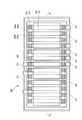
図1は、本発明の第一実施形態に係る半導体装置100の平面図である。図2(a)、(b)は、それぞれ、図1において半導体装置100をA-A’線、B-B’線に沿って切断した場合の断面図である。<First Embodiment>
[Semiconductor device configuration]
FIG. 1 is a plan view of the
半導体装置100は、主な構成要素として、基板(基材)101と、基板の一方の主面側に形成されたブリーダー抵抗回路素子102と、ブリーダー抵抗回路素子102上に形成された2つの金属膜(第一金属膜103、第二金属膜104)と、第二金属膜104の上に設けられたシリコン窒化膜105と、を有している。 The
基板101とブリーダー抵抗回路素子102の間、ブリーダー抵抗回路素子102と第一金属膜103の間、第一金属膜103と第二金属膜104の間には、それぞれ絶縁膜106、107、108が形成されている。第二金属膜104とシリコン窒化膜105の間に、絶縁膜109が形成されていてもよい。なお、図1では、主要部分となるブリーダー抵抗回路素子と、その周辺の構成を明瞭化するため、基板、絶縁膜、シリコン窒化膜等の図示を省略している。
図2に示す半導体装置100では、一方の主面側にp型ウェル101Aが設けられたn型基板101が用いられ、2層配線構造を有している。ブリーダー抵抗回路素子102は、p型ウェル101Aの表面に形成された絶縁膜(フィールド絶縁膜)106の上に設けられている。 In the
なお、半導体装置100の構成は、図2に示すものに限られることはなく、用途に応じて、ブリーダー抵抗回路素子102以外の素子が設けられていてもよく、2層以上の配線構造を有していてもよい。また、基板にドープする不純物の導電型についても、自由に設定することができる。 The configuration of the
ブリーダー抵抗回路素子102は、複数の多結晶シリコン抵抗体ユニット10からなる。多結晶シリコン抵抗体ユニット10は、p型またはn型の不純物がドープされ、所望の抵抗値を示す単体の多結晶シリコン抵抗体11、所望の抵抗値を示すように接続した複数の多結晶シリコン抵抗体11のうち、一方または両方からなる。 The bleeder
つまり、ブリーダー抵抗回路素子102は、単体の多結晶シリコン抵抗体11からなるユニット10Aのみで構成されていてもよいし、複数の多結晶シリコン抵抗体11からなるユニット10Bのみで構成されていてもよいし、ユニット10A、10Bの両方を組み合わせて構成されていてもよい。図1では、ユニット10A、10Bの両方を組み合わせて構成される場合について、例示している。 That is, the bleeder
第一金属膜103としては、例えば、Al-Si-Cuの積層膜、Al-Cuの積層膜等が用いられ、その厚さは、概ね3000Å以上5000Å以下の範囲であることが好ましい。 As the
第一金属膜103は、複数の多結晶シリコン抵抗体ユニット10の各々を、個別に覆うように複数に分割されている。つまり、いずれの多結晶シリコン抵抗体ユニット10の上にも、第一金属膜103が少なくとも一枚ずつ設けられている。隣接する抵抗体ユニット102上に設けられた第一金属膜103同士は、互いに離間している。 The
複数の第一金属膜103の各々は、多結晶シリコン抵抗体ユニット10のうち、電極部11Aを覆う部分(電極引き出し層)103Aと、電極部11A以外の高抵抗部11Bを覆う部分(カバー層)103Bとで、さらに分割されている。電極部11Aは、各多結晶シリコン抵抗体11の端部に位置し、不純物が、高抵抗部11Bよりも高い濃度でドープされている。 Each of the plurality of
図3は、半導体装置100を動作させるブリーダー抵抗回路102Aと、その周辺回路の図である。ブリーダー抵抗回路102Aは、複数の多結晶シリコン抵抗体ユニット10が、直列接続されており、特定のユニット10に対し、ヒューズ回路素子12が並列接続されている。 FIG. 3 is a diagram of a
カバー層103Bは、その各々が覆っている多結晶シリコン抵抗体ユニット10と、金属配線を介して接続されている。つまり、1つの多結晶シリコン抵抗体ユニット10に対して、それを覆う一つのカバー層103Bが電気的に接続されている。そのため、直列接続されたブリーダー抵抗回路102Aの一端側、他端側に、それぞれ異なる電源電圧Vdd、Vss(Vdd>Vss)を印加し、両者に電位差を発生させた場合であっても、カバー層103Bとユニット102とは等電位となる。The
多結晶シリコン抵抗体ユニット10とカバー層103Bとを接続する、金属配線の材料としては、第一金属膜と同じものであってもよいし、高融点金属のタングステン等であってもよい。 The material of the metal wiring connecting the
第二金属膜104としては、例えば、Al-Si-Cuの積層膜、Al-Cuの積層膜等が用いられ、その厚さは、概ね3000Å以上10000Å以下の範囲であることが好ましい。 As the
第二金属膜104は、第一金属膜103を挟んで、電極部11Aを含む複数のブリーダー抵抗回路素子102の全体を切れ目なく覆う、一体の大面積膜である。第二金属膜104の電位は、Vssに接地されている。The
本実施形態に係る半導体装置100では、複数の多結晶シリコン抵抗体ユニット10の各々に対し、個別に接続された複数の第一金属膜103を有し、さらに第一金属膜103を挟んで、ブリーダー抵抗回路素子102の全体を覆う大面積の第二金属膜104を有している。第一金属膜103を有していることにより、多結晶シリコン抵抗体ユニット10と第一金属膜103との電位差が、レイアウトによらず一定となるため、多結晶シリコン抵抗体ユニット10ごとに抵抗値変調がばらつく問題を回避することができる。 The
また、第二金属膜104を有していることにより、製造過程において、ブリーダー抵抗回路素子102に水素が浸入する問題を回避することができる。したがって、本実施形態に係る半導体装置100は、ブリーダー抵抗回路素子に含有される水素の量が、従来よりも著しく低減されたものとなる。 Further, by having the
第二金属膜104は、第一金属膜103の上層側に設けられ、第一金属膜103のように、対応する多結晶シリコン抵抗体ユニットの電極部11A、高抵抗部11Bごとに分割されている必要がなく、電極部11A周辺まで含めたブリーダー回路102A全体を、隙間なく覆う形状とすることができる。そのため、本実施形態に係る半導体装置100では、多結晶シリコン抵抗体11の高抵抗部11Bへの水素浸入経路だけでなく、電極部11Aが設けられる端部への水素浸入経路をも遮蔽することができ、ブリーダー抵抗回路素子102の抵抗分圧比の乱れに伴なった歩留り低下を防ぐことができる。 The
シリコン窒化膜105側からの平面視において、第2金属膜104の最外周は、ブリーダー抵抗回路素子102の最外周よりも外側にあることが好ましい。この場合には、ブリーダー抵抗回路素子102に対して、上層側から垂直に浸入しようとする水素に加え、斜めに浸入しようとする水素の一部を、第2金属膜104において阻止することができ、その分、水素に対する保護機能を高めることができる。 In a plan view from the
従来の構造では、高抵抗部を第一金属膜で確実に覆う必要があったため、第一金属膜は、高抵抗部だけでなく、低抵抗部の一部まで覆うように、大き目に形成されていた。つまり、従来構造では、第一金属膜には、低抵抗部とのオーバーラップ領域が存在していた。 In the conventional structure, it is necessary to surely cover the high resistance portion with the first metal film, so that the first metal film is formed to be large so as to cover not only the high resistance portion but also a part of the low resistance portion. Was there. That is, in the conventional structure, the first metal film has an overlap region with the low resistance portion.
これに対し、本実施形態に係る半導体装置100では、高抵抗部を覆う役割を第二金属膜が担うため、第一金属膜を大き目に形成する必要がなく、第一金属膜と低抵抗部とのオーバーラップ領域を削減できる分、装置全体のサイズを縮小することができる。 On the other hand, in the
また、従来構造においては、分割した第一金属膜同士の隙間のところにダミーの抵抗体が配置されていたが、本実施形態ではその必要がない分、さらに、装置全体のサイズを縮小することができる。 Further, in the conventional structure, a dummy resistor is arranged in the gap between the divided first metal films, but in the present embodiment, the size of the entire device is further reduced because it is not necessary. Can be done.
[半導体装置の製造方法]
半導体製造装置100の製造方法について、ブリーダー抵抗回路素子102とその周辺部分を形成する工程を中心として説明する。[Manufacturing method of semiconductor devices]
The manufacturing method of the
まず、n型の基板の一方の主面側に、p型不純物をドープしてp型ウェルを形成する。続いて、LOCOS(Local Oxidation of Silicon)法またはSTI(Shallow Trench Isolation)法により、フィールド絶縁膜を形成する。続いて、p型ウェル内の所定の位置に、相対的にp型不純物濃度が高い領域(p+拡散層)を形成する。First, a p-type impurity is doped on one main surface side of an n-type substrate to form a p-type well. Subsequently, a field insulating film is formed by the LOCOS (Local Oxidation of Silicon) method or the STI (Shallow Trench Isolation) method. Subsequently, a region (p+ diffusion layer) having a relatively high p-type impurity concentration is formed at a predetermined position in the p-type well.
次に、フィールド絶縁膜上に、CVD法等の公知の方法により、ブリーダー抵抗回路を構成する多結晶シリコン(ポリシリコン)の膜形成を行い、さらに、所望の形状、配置となるようにパターニングを行って、複数の多結晶シリコン抵抗体を形成する。形成する抵抗体の厚さは、概ね500Å以上5000Å以下とするのが好ましい。 Next, a polycrystalline silicon (polysilicon) film constituting the bleeder resistance circuit is formed on the field insulating film by a known method such as a CVD method, and further patterned so as to have a desired shape and arrangement. This is done to form a plurality of polycrystalline silicon resistors. The thickness of the resistor to be formed is preferably about 500 Å or more and 5000 Å or less.
次に、多結晶シリコン抵抗体上に、CVD法等の公知の方法により、層間絶縁膜を形成する。続いて、単数または複数の多結晶シリコン抵抗体で構成される、多結晶シリコン抵抗体ユニットの少なくとも一部と重なる位置において、層間絶縁膜内にコンタクトホールを形成する。続いて、コンタクトホール内に金属膜を埋め込む。埋め込む金属膜の材料としては、第一金属膜の材料と同じものであってもよいし、高融点金属のタングステンであってもよい。 Next, an interlayer insulating film is formed on the polycrystalline silicon resistor by a known method such as a CVD method. Subsequently, a contact hole is formed in the interlayer insulating film at a position overlapping with at least a part of the polycrystalline silicon resistor unit composed of one or more polycrystalline silicon resistors. Subsequently, a metal film is embedded in the contact hole. The material of the metal film to be embedded may be the same as the material of the first metal film, or may be tungsten, which is a refractory metal.
次に、コンタクトホールが形成された層間絶縁膜上に、スパッタリング法等の公知の方法により第一金属膜を形成する。そして、形成した第一金属膜を、多結晶シリコン抵抗体ユニットごとに1対1で対応するように、パターニングを行って分割する。この分割により、多結晶シリコン抵抗体ユニットごとに、対応する第一金属膜のカバー層が形成される。つまり、一つの多結晶シリコン抵抗体ユニットを、一つの第一金属膜がカバーした状態となる。 Next, a first metal film is formed on the interlayer insulating film in which the contact hole is formed by a known method such as a sputtering method. Then, the formed first metal film is patterned and divided so as to have a one-to-one correspondence for each polycrystalline silicon resistor unit. By this division, the cover layer of the corresponding first metal film is formed for each polycrystalline silicon resistor unit. That is, one polycrystalline silicon resistor unit is covered with one first metal film.
第一金属膜としては、例えば、Al-Si-Cuの積層膜、Al-Cuの積層膜を用いることができる。第一金属膜103の厚さは、概ね3000Å以上5000Å以下の範囲で設定することが好ましい。 As the first metal film, for example, an Al—Si—Cu laminated film or an Al—Cu laminated film can be used. The thickness of the
次に、第一金属膜上に、CVD法等の公知の方法により層間絶縁膜を形成し、この層間絶縁膜の上に、スパッタリング法等の公知の方法により第二金属膜を形成する。このとき、少なくともブリーダー抵抗回路素子の全体を覆う、一体の大面積を有する膜となるようにする。 Next, an interlayer insulating film is formed on the first metal film by a known method such as a CVD method, and a second metal film is formed on the interlayer insulating film by a known method such as a sputtering method. At this time, the film has a large integrated area and covers at least the entire bleeder resistance circuit element.
第二金属膜としては、例えば、Al-Si-Cuの積層膜、Al-Cuの積層膜を用いることができる。第二金属膜の厚さは、概ね3000Å以上10000Å以下の範囲で設定することが好ましい。 As the second metal film, for example, an Al—Si—Cu laminated film or an Al—Cu laminated film can be used. The thickness of the second metal film is preferably set in the range of approximately 3000 Å or more and 10000 Å or less.
最後に、第二金属膜上に、プラズマCVD法により、直接または酸化膜を介して、シリコン窒化膜を形成することによって、本実施形態に係る半導体装置100を得ることができる。 Finally, the
<第二実施形態>
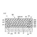
[半導体装置の構成]
図4は、本発明の第二実施形態に係る半導体装置200の平面図である。図5は、図4において半導体装置200をC-C’線に沿って切断した場合の断面図である。なお、図4では、主要部分となるブリーダー抵抗回路素子と、その周辺の構成を明瞭化するため、基板、絶縁膜、シリコン窒化膜等の図示を省略している。<Second embodiment>
[Semiconductor device configuration]
FIG. 4 is a plan view of the
半導体装置200は、ブリーダー抵抗回路素子202の周囲(最外周)に立設され、頂部が第二金属膜204に接続され、底部が基板201に接続された側壁部211を有している。基板201の表面のうち側壁部211が接続される部分に、p型高濃度拡散層(p+拡散層)210が設けられている。半導体装置200の側壁部211以外の構成については、第一実施形態に係る半導体装置100の構成と同様であり、半導体装置100と同等の効果を得ることができる。The
側壁部211は、第一金属膜203Cと、その下層側および上層側の絶縁膜207、208に設けられたコンタクトホール(第一接続孔207A、第二接続孔208A)にそれぞれ埋め込まれた金属膜207B、208B、第一接続孔207Aの下のp型ウェル201A内に設けられたp型高濃度拡散層(p+拡散層)210とで、スタック状に構成されている。第一接続孔207Aは基板201と第一金属膜203Cとを連結し、第二接続孔208Aは第一金属膜203Cと第二金属膜204とを連結している。p型高濃度拡散層210は、半導体装置200の最表面側からの平面視において、ブリーダー抵抗回路素子202の周囲を取り囲んでいる。The
シリコン窒化膜205側からの平面視において、側壁部211は、短い間隔で並んでいることが好ましく、ブリーダー抵抗回路素子202を切れ目なく囲んでいれば、より好ましい。 In a plan view from the
半導体装置200は、側壁部211があることにより、上方から直線的に浸入する水素だけでなく、側方から回り込んで浸入する水素をも阻止することができ、ブリーダー抵抗回路素子102をより強力に保護することができる。 Due to the presence of the
また、側壁部211が側方からの水素浸入を遮蔽するため、第二金属膜は、上方から直線的に浸入する水素だけを遮蔽すればよい。したがって、第二金属膜の面積は、ブリーダ抵抗素子と同程度の面積とすることができ、側壁部211がない場合に比べて、装置全体のサイズを縮小することができる。 Further, since the
<第三実施形態>
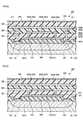
[半導体装置の構成]
図6は、本発明の第三実施形態に係る半導体装置300の平面図である。図7(a)、(b)は、それぞれ、図6において半導体装置300をD-D’線、E-E’線に沿って切断した場合の断面図である。なお、図6では、主要部分となるブリーダー抵抗回路素子と、その周辺の構成を明瞭化するため、基板、絶縁膜、シリコン窒化膜等の図示を省略している。<Third embodiment>
[Semiconductor device configuration]
FIG. 6 is a plan view of the
半導体装置300は、第二実施形態と同様に、ブリーダー抵抗回路素子302の周囲(最外周)に立設され、頂部が第二金属膜304に接続され、底部が基板301に接続された側壁部311を有している。また、半導体装置300の側壁部311が形成されている領域の内側のブリーダー抵抗回路素子302の構成については、第一実施形態に係る半導体装置100の構成と同様である。 Similar to the second embodiment, the
図7(a)に示すように、側壁部311は、第一金属膜303Cと、その下層側および上層側の絶縁膜307、308に設けられたコンタクトホール(第一接続孔307A、第二接続孔308A)にそれぞれ埋め込まれた金属膜307B、308B、第一接続孔307Aの下のp型ウェル301A内に設けられたp型高濃度拡散層(p+拡散層)310とで、スタック状に構成されていることも第二実施形態と同様である。そして、第一接続孔307Aは、基板301と第一金属膜303Cとを連結し、第二接続孔308Aは、第一金属膜303Cと第二金属膜304とを連結している。p型高濃度拡散層310は、半導体装置300の最表面側からの平面視において、ブリーダー抵抗回路素子302の周囲を取り囲んでいる。すなわち、これらの構成により第一実施形態と第二実施形態と同等の効果を得ることができる。As shown in FIG. 7A, the
図6のE-E’線の近傍においては、電極部31Aに接続される電極引き出し層303Aを図示しない他の回路素子部分と接続させるために、電極引き出し層303Aがブリーダー抵抗回路素子302の外側に向かって延設される部分において、側壁部311は、切れ目を有している。 In the vicinity of the EE'line of FIG. 6, in order to connect the electrode pull-out
そこで、第三実施形態においてはさらに、半導体装置300は、ブリーダー抵抗回路素子302が形成されている領域と、側壁部311が形成されている領域との間の領域に、多結晶シリコンカバー32を有している。多結晶シリコンカバー32は、側壁部311に切れ目が存在する部分に、平面視においてその側壁部311の切れ目を補うようにブリーダー抵抗回路素子302の外側の領域に配置される。図6においては、多結晶シリコンカバー32がブリーダー抵抗回路素子302の外側の領域において電極部31Aが配置されている右側と左側の側面に対し平行に、且つ直線的に設けられている。 Therefore, in the third embodiment, the
図7(b)の断面図に示すように、多結晶シリコンカバー32は、多結晶シリコン抵抗体31の両側のフィールド絶縁膜306上に、多結晶シリコン抵抗体31と同一の多結晶シリコン層で形成されている。多結晶シリコンカバー32の上には、電極引き出し層303が、第二金属膜304が形成されている領域よりもさらに外側に延設されており、ここに側壁部311を形成することはできない。そのため、この側壁部311の切れ目を通って、多結晶シリコン抵抗体31へ水素が侵入する可能性がある。多結晶シリコンカバー32は、側壁部311の切れ目を通って浸入してくる水素を吸収し、多結晶シリコン抵抗体31に到達する水素を低減させることができる。 As shown in the cross-sectional view of FIG. 7B, the
一般に多結晶シリコンは、単結晶シリコンと異なり、シリコン原子が規則正しく結合した結晶性の高いグレイン部分と、その境界部分でありシリコン原子の並びが不規則で結晶性が低いグレイン境界部分とから構成される。グレイン境界部分には多数の未結合手をもつ原子が存在する。原子の未結合手には水素が結合しやすいので、その結合バラつきによって多結晶シリコン抵抗体の抵抗値がバラつく。図6における多結晶シリコンカバー32は、この性質を利用し、ブリーダー抵抗回路素子302の外側の領域に配置することで、多結晶シリコンカバー32の外側から浸入する水素を吸収し、多結晶シリコンカバー32が形成される領域よりも内側の領域への水素の侵入を抑制する。 In general, polysilicon is composed of a highly crystalline grain portion in which silicon atoms are regularly bonded and a grain boundary portion in which silicon atoms are irregularly arranged and have low crystallinity, unlike single crystal silicon. To. There are many unbonded atoms at the grain boundary. Since hydrogen is easily bonded to the unbonded hands of an atom, the resistance value of the polycrystalline silicon resistor varies depending on the bond variation. Utilizing this property, the
半導体装置300は、第2金属膜304と側壁部311に加え、側壁部311の切れ目に多結晶シリコンカバー32を備えることによって、外部からの水素の浸入を抑制し、ブリーダー抵抗回路素子302を第二実施形態よりも強力に保護することができる。 The
図6において、多結晶シリコンカバー32は、ブリーダー抵抗回路素子302の外側の領域において、電極部31Aが配置されている右側と左側の側面の前面に対し平行に、且つ直線的に設けられているが、この構成に限られるものではない。すなわち、側壁部311の切れ目に部分的に配置されていても構わない。また、平面視において、ブリーダー抵抗回路素子302の外側の領域の電極部31Aが配置されていない上側と下側の側面に沿った部分に側壁部311の切れ目があればその部分に多結晶シリコンカバー32を配置する。一方、多結晶シリコンカバー32を、ブリーダー抵抗回路素子302の周囲全てを囲うように切れ目無く配置しても構わない。そうすることであらゆる方向からの意図しない水素の浸入を抑制し、多結晶シリコン抵抗体31の抵抗値バラつきを抑制することができる。 In FIG. 6, the
また、多結晶シリコンカバー32は、多結晶シリコン抵抗体31よりも厚さが厚い方が、水素浸入方向を減らすことができるので水素の遮蔽効果が高い。図7(a)、(b)においては、多結晶シリコン抵抗体31と多結晶シリコンカバー32を同一の多結晶シリコン層で形成している。そのため、両者の厚さを異ならせることができないが、多結晶シリコンカバー32を多結晶シリコン抵抗体31とは別の多結晶シリコン層で形成することで厚さの違いを実現できる。多結晶シリコン抵抗体31と別の多結晶シリコン層であり、厚さが多結晶シリコン抵抗体よりも厚いのであれば、例えば、電界効果型トランジスタのゲート電極に使われる多結晶シリコン層や、抵抗値を調整するヒューズに使われる多結晶シリコン層を利用してもよい(不図示)。 Further, when the thickness of the
100、200、300・・・半導体装置
101、201、301・・・基板(n型基板)
101A、201A、301A・・・p型ウェル
102、202、302・・・ブリーダー抵抗回路素子
103、203、203C、303、303C・・・第一金属膜
103A、203A、303A・・・電極引き出し層
103B、203B、303B・・・カバー層
104、204、304・・・第二金属膜
105、205、305・・・シリコン窒化膜
106、206、306・・・絶縁膜(フィールド絶縁膜)
107、207、307・・・絶縁膜
108、208、308・・・絶縁膜
109、209、309・・・絶縁膜
210、310・・・p型高濃度拡散層
211、311・・・側壁部
10、10A、10B・・・多結晶シリコン抵抗体ユニット
11、21、31・・・多結晶シリコン抵抗体
11A、21A、31A・・・電極部
11B、21B、31B・・・高抵抗部
32・・・多結晶シリコンカバー
207A、307A・・・第一接続孔
207B、307B・・・金属膜
208A、308A・・・第二接続孔
208B、308B・・・金属膜100, 200, 300 ...
101A, 201A, 301A ... p-
107, 207, 307 ... Insulating
Claims (4)
Translated fromJapanese前記基板の一方の主面側に形成され、複数の多結晶シリコン抵抗体ユニットからなるブリーダー抵抗回路素子と、
前記複数の多結晶シリコン抵抗体ユニットの各々を、個別に覆うように複数に分割された第一金属膜と、
前記第一金属膜の上に、前記ブリーダー抵抗回路素子の全体を覆う一体の第二金属膜と、
前記第二金属膜の上に形成されたシリコン窒化膜と、
前記シリコン窒化膜側からの平面視において、前記ブリーダー抵抗回路素子の周囲に立設され、前記第二金属膜に接続された側壁部と、
を有し、
複数の前記第一金属膜の各々は、前記多結晶シリコン抵抗体ユニットのうち、電極部を覆う部分と、電極部以外を覆う部分とで構成されており、
前記電極部以外を覆う前記第一金属膜は、各々覆っている前記多結晶シリコン抵抗体ユニットと、電気的に接続されていることを特徴とする半導体装置。With the board
A bleeder resistance circuit element formed on one main surface side of the substrate and composed of a plurality of polycrystalline silicon resistor units,
A first metal film divided into a plurality of pieces so as to individually cover each of the plurality of polycrystalline silicon resistor units.
On the first metal film, an integral second metal film that covers the entire bleeder resistance circuit element, and
The silicon nitride film formed on the second metal film and
In a plan view from the silicon nitride film side, a side wall portion erected around the bleeder resistance circuit element and connected to the second metal film, and a side wall portion.
Have,
Each of the plurality of first metal films is composed of a portion of the polycrystalline silicon resistor unit that covers the electrode portion and a portion that covers the portion other than the electrode portion.
A semiconductor device characterized in that the first metal film covering other than the electrode portion is electrically connected to the polycrystalline silicon resistor unit covering each of the first metal films.
前記側壁部が、前記第一接続孔に埋め込まれた金属膜と、前記第二接続孔に埋め込まれた金属膜とで構成されていることを特徴とする請求項1又は2に記載の半導体装置。The semiconductor device according to claim 1 or 2, wherein the side wall portion is composed of a metal film embedded in the first connection hole and a metal film embedded in the second connection hole. ..
Priority Applications (4)
| Application Number | Priority Date | Filing Date | Title |
|---|---|---|---|
| US15/916,012US20180269270A1 (en) | 2017-03-14 | 2018-03-08 | Semiconductor device |
| KR1020180028674AKR20180105080A (en) | 2017-03-14 | 2018-03-12 | Semiconductor device |
| TW107108189ATWI782959B (en) | 2017-03-14 | 2018-03-12 | Semiconductor device |
| CN201810201159.8ACN108573958A (en) | 2017-03-14 | 2018-03-12 | Semiconductor device |
Applications Claiming Priority (2)
| Application Number | Priority Date | Filing Date | Title |
|---|---|---|---|
| JP2017048801 | 2017-03-14 | ||
| JP2017048801 | 2017-03-14 |
Publications (2)
| Publication Number | Publication Date |
|---|---|
| JP2018152545A JP2018152545A (en) | 2018-09-27 |
| JP7010668B2true JP7010668B2 (en) | 2022-01-26 |
Family
ID=63680515
Family Applications (1)
| Application Number | Title | Priority Date | Filing Date |
|---|---|---|---|
| JP2017215445AActiveJP7010668B2 (en) | 2017-03-14 | 2017-11-08 | Semiconductor device |
Country Status (3)
| Country | Link |
|---|---|
| JP (1) | JP7010668B2 (en) |
| KR (1) | KR20180105080A (en) |
| TW (1) | TWI782959B (en) |
Families Citing this family (4)
| Publication number | Priority date | Publication date | Assignee | Title |
|---|---|---|---|---|
| JP7115951B2 (en)* | 2018-09-28 | 2022-08-09 | エイブリック株式会社 | Semiconductor device and its manufacturing method |
| JP7489872B2 (en)* | 2019-10-31 | 2024-05-24 | エイブリック株式会社 | Semiconductor Device |
| JP7638182B2 (en)* | 2021-09-02 | 2025-03-03 | ルネサスエレクトロニクス株式会社 | Semiconductor Device |
| DE112022006051T5 (en)* | 2021-12-17 | 2025-02-13 | Rohm Co., Ltd. | SEMICONDUCTOR COMPONENT AND METHOD FOR THE PRODUCTION THEREOF |
Citations (3)
| Publication number | Priority date | Publication date | Assignee | Title |
|---|---|---|---|---|
| JP2004281966A (en) | 2003-03-19 | 2004-10-07 | Ricoh Co Ltd | Semiconductor device and method of manufacturing semiconductor device |
| JP2006032585A (en) | 2004-07-15 | 2006-02-02 | Seiko Instruments Inc | Semiconductor integrated circuit device |
| JP2010016059A (en) | 2008-07-01 | 2010-01-21 | Seiko Instruments Inc | Method of manufacturing semiconductor device |
Family Cites Families (9)
| Publication number | Priority date | Publication date | Assignee | Title |
|---|---|---|---|---|
| JP3195828B2 (en)* | 1992-08-31 | 2001-08-06 | 三菱電機株式会社 | Semiconductor device |
| US5530418A (en)* | 1995-07-26 | 1996-06-25 | Taiwan Semiconductor Manufacturing Company | Method for shielding polysilicon resistors from hydrogen intrusion |
| JP3526701B2 (en)* | 1995-08-24 | 2004-05-17 | セイコーインスツルメンツ株式会社 | Semiconductor device |
| US6232194B1 (en)* | 1999-11-05 | 2001-05-15 | Taiwan Semiconductor Manufacturing Company | Silicon nitride capped poly resistor with SAC process |
| JP4162515B2 (en)* | 2002-03-25 | 2008-10-08 | セイコーインスツル株式会社 | Semiconductor device and manufacturing method thereof |
| JP4141407B2 (en)* | 2003-06-11 | 2008-08-27 | 株式会社リコー | Manufacturing method of semiconductor device |
| WO2006036000A1 (en)* | 2004-09-30 | 2006-04-06 | Ricoh Company, Ltd. | Semiconductor device and fabrication process thereof |
| JP2006332428A (en)* | 2005-05-27 | 2006-12-07 | Seiko Instruments Inc | Semiconductor integrated circuit device |
| EP2491585B1 (en)* | 2009-10-21 | 2020-01-22 | Semiconductor Energy Laboratory Co. Ltd. | Semiconductor device |
- 2017
- 2017-11-08JPJP2017215445Apatent/JP7010668B2/enactiveActive
- 2018
- 2018-03-12KRKR1020180028674Apatent/KR20180105080A/ennot_activeWithdrawn
- 2018-03-12TWTW107108189Apatent/TWI782959B/ennot_activeIP Right Cessation
Patent Citations (3)
| Publication number | Priority date | Publication date | Assignee | Title |
|---|---|---|---|---|
| JP2004281966A (en) | 2003-03-19 | 2004-10-07 | Ricoh Co Ltd | Semiconductor device and method of manufacturing semiconductor device |
| JP2006032585A (en) | 2004-07-15 | 2006-02-02 | Seiko Instruments Inc | Semiconductor integrated circuit device |
| JP2010016059A (en) | 2008-07-01 | 2010-01-21 | Seiko Instruments Inc | Method of manufacturing semiconductor device |
Also Published As
| Publication number | Publication date |
|---|---|
| KR20180105080A (en) | 2018-09-27 |
| JP2018152545A (en) | 2018-09-27 |
| TWI782959B (en) | 2022-11-11 |
| TW201834200A (en) | 2018-09-16 |
Similar Documents
| Publication | Publication Date | Title |
|---|---|---|
| JP7010668B2 (en) | Semiconductor device | |
| TWI540725B (en) | Semiconductor device and method of manufacturing the same | |
| US20080230820A1 (en) | Semiconductor device | |
| US7999333B2 (en) | Semiconductor device | |
| JP2009147150A (en) | Semiconductor device | |
| US9349844B2 (en) | Semiconductor device manufacturing method | |
| CN101685818A (en) | Semiconductor device | |
| JP2002124681A (en) | Semiconductor device | |
| US6661076B2 (en) | Semiconductor device | |
| JP2018200916A (en) | Semiconductor device | |
| US20180269270A1 (en) | Semiconductor device | |
| JP7236944B2 (en) | Semiconductor device and its manufacturing method | |
| JP2020202356A (en) | Resistor element and manufacturing method for the same | |
| US20240304524A1 (en) | Semiconductor device | |
| JP2010087336A (en) | Semiconductor integrated circuit | |
| JP2008218818A (en) | Semiconductor device | |
| JP2011044622A (en) | Semiconductor device | |
| JP2003017704A (en) | Semiconductor device | |
| CN100474588C (en) | Semiconductor device | |
| JP2007165693A (en) | Semiconductor device | |
| JP2002222918A (en) | Semiconductor device | |
| JP4179814B2 (en) | Semiconductor device | |
| JP2009032730A (en) | Semiconductor device | |
| JP2021125614A (en) | Semiconductor devices and their manufacturing methods | |
| JP2006013056A (en) | Semiconductor integrated circuit device and circuit wiring method |
Legal Events
| Date | Code | Title | Description |
|---|---|---|---|
| A621 | Written request for application examination | Free format text:JAPANESE INTERMEDIATE CODE: A621 Effective date:20201013 | |
| A977 | Report on retrieval | Free format text:JAPANESE INTERMEDIATE CODE: A971007 Effective date:20210730 | |
| A131 | Notification of reasons for refusal | Free format text:JAPANESE INTERMEDIATE CODE: A131 Effective date:20210824 | |
| A521 | Request for written amendment filed | Free format text:JAPANESE INTERMEDIATE CODE: A523 Effective date:20211005 | |
| TRDD | Decision of grant or rejection written | ||
| A01 | Written decision to grant a patent or to grant a registration (utility model) | Free format text:JAPANESE INTERMEDIATE CODE: A01 Effective date:20220111 | |
| A61 | First payment of annual fees (during grant procedure) | Free format text:JAPANESE INTERMEDIATE CODE: A61 Effective date:20220113 | |
| R150 | Certificate of patent or registration of utility model | Ref document number:7010668 Country of ref document:JP Free format text:JAPANESE INTERMEDIATE CODE: R150 | |
| S531 | Written request for registration of change of domicile | Free format text:JAPANESE INTERMEDIATE CODE: R313531 | |
| R350 | Written notification of registration of transfer | Free format text:JAPANESE INTERMEDIATE CODE: R350 |