JP7009711B2 - Doherty amp - Google Patents
Doherty ampDownload PDFInfo
- Publication number
- JP7009711B2 JP7009711B2JP2017230714AJP2017230714AJP7009711B2JP 7009711 B2JP7009711 B2JP 7009711B2JP 2017230714 AJP2017230714 AJP 2017230714AJP 2017230714 AJP2017230714 AJP 2017230714AJP 7009711 B2JP7009711 B2JP 7009711B2
- Authority
- JP
- Japan
- Prior art keywords
- output
- amplifier
- transmission line
- peak
- carrier
- Prior art date
- Legal status (The legal status is an assumption and is not a legal conclusion. Google has not performed a legal analysis and makes no representation as to the accuracy of the status listed.)
- Active
Links
- 230000005540biological transmissionEffects0.000claimsdescription98
- 230000008878couplingEffects0.000claimsdescription17
- 238000010168coupling processMethods0.000claimsdescription17
- 238000005859coupling reactionMethods0.000claimsdescription17
- 230000003111delayed effectEffects0.000description8
- 230000003071parasitic effectEffects0.000description8
- 238000010586diagramMethods0.000description7
- 229920006395saturated elastomerPolymers0.000description5
- 230000003321amplificationEffects0.000description4
- 238000003199nucleic acid amplification methodMethods0.000description4
- 230000001934delayEffects0.000description2
- 230000005669field effectEffects0.000description2
- 238000000034methodMethods0.000description2
- 238000010295mobile communicationMethods0.000description2
- 230000015572biosynthetic processEffects0.000description1
- 239000003990capacitorSubstances0.000description1
- 238000006243chemical reactionMethods0.000description1
- 238000004891communicationMethods0.000description1
- 239000002131composite materialSubstances0.000description1
- 230000000694effectsEffects0.000description1
- 230000007774longtermEffects0.000description1
- 238000012986modificationMethods0.000description1
- 230000004048modificationEffects0.000description1
- 238000003786synthesis reactionMethods0.000description1
Images


Classifications
- H—ELECTRICITY
- H03—ELECTRONIC CIRCUITRY
- H03F—AMPLIFIERS
- H03F1/00—Details of amplifiers with only discharge tubes, only semiconductor devices or only unspecified devices as amplifying elements
- H03F1/02—Modifications of amplifiers to raise the efficiency, e.g. gliding Class A stages, use of an auxiliary oscillation
- H03F1/0205—Modifications of amplifiers to raise the efficiency, e.g. gliding Class A stages, use of an auxiliary oscillation in transistor amplifiers
- H03F1/0288—Modifications of amplifiers to raise the efficiency, e.g. gliding Class A stages, use of an auxiliary oscillation in transistor amplifiers using a main and one or several auxiliary peaking amplifiers whereby the load is connected to the main amplifier using an impedance inverter, e.g. Doherty amplifiers
- H—ELECTRICITY
- H03—ELECTRONIC CIRCUITRY
- H03F—AMPLIFIERS
- H03F3/00—Amplifiers with only discharge tubes or only semiconductor devices as amplifying elements
- H03F3/20—Power amplifiers, e.g. Class B amplifiers, Class C amplifiers
- H—ELECTRICITY
- H03—ELECTRONIC CIRCUITRY
- H03F—AMPLIFIERS
- H03F3/00—Amplifiers with only discharge tubes or only semiconductor devices as amplifying elements
- H03F3/20—Power amplifiers, e.g. Class B amplifiers, Class C amplifiers
- H03F3/21—Power amplifiers, e.g. Class B amplifiers, Class C amplifiers with semiconductor devices only
- H03F3/211—Power amplifiers, e.g. Class B amplifiers, Class C amplifiers with semiconductor devices only using a combination of several amplifiers
- H—ELECTRICITY
- H03—ELECTRONIC CIRCUITRY
- H03F—AMPLIFIERS
- H03F3/00—Amplifiers with only discharge tubes or only semiconductor devices as amplifying elements
- H03F3/30—Single-ended push-pull [SEPP] amplifiers; Phase-splitters therefor
- H03F3/3001—Single-ended push-pull [SEPP] amplifiers; Phase-splitters therefor with field-effect transistors
- H03F3/3044—Junction FET SEPP output stages
- H03F3/305—Junction FET SEPP output stages with symmetrical driving of the end stage
- H—ELECTRICITY
- H03—ELECTRONIC CIRCUITRY
- H03F—AMPLIFIERS
- H03F3/00—Amplifiers with only discharge tubes or only semiconductor devices as amplifying elements
- H03F3/60—Amplifiers in which coupling networks have distributed constants, e.g. with waveguide resonators
- H03F3/602—Combinations of several amplifiers
- H—ELECTRICITY
- H03—ELECTRONIC CIRCUITRY
- H03F—AMPLIFIERS
- H03F2200/00—Indexing scheme relating to amplifiers
- H03F2200/192—A hybrid coupler being used at the input of an amplifier circuit
- H—ELECTRICITY
- H03—ELECTRONIC CIRCUITRY
- H03F—AMPLIFIERS
- H03F2200/00—Indexing scheme relating to amplifiers
- H03F2200/405—Indexing scheme relating to amplifiers the output amplifying stage of an amplifier comprising more than three power stages
- H—ELECTRICITY
- H03—ELECTRONIC CIRCUITRY
- H03F—AMPLIFIERS
- H03F2200/00—Indexing scheme relating to amplifiers
- H03F2200/451—Indexing scheme relating to amplifiers the amplifier being a radio frequency amplifier
Landscapes
- Engineering & Computer Science (AREA)
- Power Engineering (AREA)
- Amplifiers (AREA)
Description
Translated fromJapanese本発明はピークアンプを複数備えるドハティアンプに関する。 The present invention relates to a Doherty amplifier including a plurality of peak amplifiers.
大概の通信システムでは、高効率と高線形性の両立がパワーアンプに要求されているが、効率と線形性はトレードオフの関係にある。さらに、移動通信の第2世代方式に属するGSM(Global System for Mobile Communications:携帯通信のための全地球システム)/及びその拡張型で第3世代の方式に属するEDGE(Enhanced data GSM Environment:高度データGSM環境)、あるいは、第3世代に属するWDCMA(Wideband Code Division Multiple Access:広帯域コード分割多チャンネルアクセス)/第4世代に属するLTE(Long Term Evolution:長期的進化)の各規格では、パワーアンプに広ダイナミックレンジ出力を要請する。最大出力で最高効率を発揮するパワーアンプを基地局向けに設計すると、低出力時にはその効率が低下してしまう。故に、基地局パワーアンプに対して、最大出力時のみならず、-6dB以下といった低出力時にも効率と線形性の両立をデジタル制御かつ低コストで実現するのは容易ではない。 In most communication systems, power amplifiers are required to have both high efficiency and high linearity, but efficiency and linearity are in a trade-off relationship. In addition, GSM (Global System for Mobile Communications), which belongs to the second generation method of mobile communication, and EDGE (Enhanced data GSM Environment: advanced data), which is an extended version of it and belongs to the third generation method, In each standard of WDCMA (Wideband Code Division Multiple Access) belonging to the 3rd generation or LTE (Long Term Evolution) belonging to the 4th generation, it is used as a power amplifier. Request wide dynamic range output. If a power amplifier that exhibits maximum efficiency at maximum output is designed for a base station, its efficiency will decrease at low output. Therefore, it is not easy for the base station power amplifier to achieve both efficiency and linearity at low cost with digital control not only at the maximum output but also at a low output such as -6 dB or less.
ピークアンプを複数備えるドハティアンプでは、ピークアンプの出力を合成する出力合成器の構成が複雑となる。特に、低出力領域でオフされたピークアンプの出力をそのまま合成する回路では、アンプに付随する寄生容量、寄生インダクタンス、等の影響を受け、ピークアンプの出力を厳密にはオープンと見なせないことがある。その場合、オープンを前提とする出力結合ユニットでは所定の動作が期待できず、また、ドハティアンプ全体としての効率低下を招いてしまう。 In a Doherty amplifier having a plurality of peak amplifiers, the configuration of an output synthesizer that synthesizes the outputs of the peak amplifiers becomes complicated. In particular, in a circuit that synthesizes the output of a peak amplifier that is turned off in the low output region as it is, the output of the peak amplifier cannot be strictly regarded as open due to the influence of parasitic capacitance, parasitic inductance, etc. associated with the amplifier. There is. In that case, a predetermined operation cannot be expected in the output coupling unit that is premised on being open, and the efficiency of the Doherty amplifier as a whole is lowered.
本発明に係るドハティアンプは、1つのキャリアアンプと第1~第3のピークアンプを備え、入力分配器と、アンプユニットと、オフセットユニットと、出力結合器を含む。入力分配器は、入力信号をキャリアアンプと第1~第3のピークアンプに等しく分配する。アンプユニットは、これらキャリアアンプと第1~第3のピークアンプを含む。オフセットユニットは、キャリアアンプの出力に接続されたキャリアオフセット伝送線路と第1~第3のピークアンプそれぞれの出力に接続された第1~第3のオフセット伝送線路を有する。出力結合器はこれらキャリアオフセット伝送線路および第1~第3のオフセット伝送線路の出力を結合する複数の結合伝送線路を含む。本発明に係るドハティアンプでは、キャリアオフセット伝送線路および第1~第3のオフセット伝送線路がそれぞれキャリアアンプ及び第1~第3のピークアンプがオフされている時の出力インピーダンスをショート状態に変換する伝送線路である。また、出力結合器は結合ノードを含み、キャリアオフセット伝送線路の出力は直接に、第1のピークアンプの出力に接続した第1のオフセット伝送線路の出力は第1の結合伝送線路を介して、第2のピークアンプの出力に接続した第2のオフセット伝送線路の出力は、第2の結合伝送線路及び第1の結合伝送線路を介して、第3のピークアンプの出力に接続した第3のオフセット伝送線路の出力は第3の結合伝送線路を介して、それぞれ結合ノードに接続する。The Doherty amplifier according to the present invention includesone carrier amplifier andfirst to third peak amplifiers, and includes an input distributor, an amplifier unit, an offset unit, and an output coupler. The input distributor distributes the input signal equally to the carrier amplifier andthe first to third peak amplifiers. The amplifier unit includes these carrier amplifiers andfirst to third peak amplifiers. The offset unit hasa carrier offset transmission line connected to the output of the carrier amplifier and a first to third offset transmission linesconnected to the outputs ofthe first to third peak amplifiers, respectively. The output coupler includes a plurality of coupled transmission lines that combine the outputs of thesecarrier offset transmission lines and the first to third offset transmission lines. In the Doherty amplifier according to the present invention, thecarrier offset transmission line and the first to third offset transmission lines convert the output impedance when the carrier amplifier andthe first to third peak amplifiers are off, respectively, into a short state. It is a transmission line.Also, the output combiner includes a coupling node, the output of the carrier offset transmission line is directly connected to the output of the first peak amplifier, and the output of the first offset transmission line is via the first coupled transmission line. The output of the second offset transmission line connected to the output of the second peak amplifier is a third connected to the output of the third peak amplifier via the second coupled transmission line and the first coupled transmission line. The output of the offset transmission line is connected to the combined node via the third combined transmission line.
それぞれのアンプの出力がオープン状態の各アンプの出力インピーダンスを一旦ショートに変換するため、出力結合器における結合機能の安定化を図ることができる。 Since the output impedance of each amplifier in the open state of each amplifier is once converted to a short circuit, it is possible to stabilize the coupling function in the output coupler.
本願発明に係るドハティアンプの具体例を、以下に添付の図面を参照しながら詳細に説明する。なお、本発明は、これら例示に限定されるものではなく、特許請求の範囲によって示され、また、特許請求の範囲と均等の意味および範囲内での全ての変更が含まれることが意図されている。 Specific examples of the Doherty amplifier according to the present invention will be described in detail below with reference to the accompanying drawings. It should be noted that the present invention is not limited to these examples, but is shown by the scope of claims, and is intended to include all modifications within the meaning and scope equivalent to the scope of claims. There is.
特許文献1は多段のドハティ増幅に構成を開示している。特許文献1に開示されたドハティアンプ100は、図1の機能ブロックが示す様に、それ以前に知られていた構成を有する。キャリアアンプ100とピークアンプ101~103を有する一般的なドハティアンプの出力を、複数のλ/4伝送線路TLC~TL2を介して順次接続する構成を備える。ここで、アンプ100はキャリアアンプであり、アンプ10n(n=1~3)はピークアンプである。飽和出力時には全てのアンプ100~103がオン状態にあり、飽和出力より12dB以上小さい時にキャリアアンプ100のみがオン、ピークアンプ101~103の出力全てがオープン状態となるため、伝送線路TL1によりノードN1がショートとみなされ、ノードN0から見込んだピークアンプ101~103は全てオープンとみなせる。出力端子RFOUTに50Ωの負荷が接続された場合に、キャリアアンプ100の負荷インピーダンスは502/(252/50)=200Ωで与えられる。飽和出力に対し-12dB~-6dBの出力では、キャリアアンプ100とピークアンプ101がオンとなり、その時のキャリアアンプ100から負荷を見込んだインピーダンスと、ピークアンプ101から負荷を見込んだインピーダンスはともに100Ωとなり、ノードN0から負荷を見込んだインピーダンスは12.5Ωとなって出力端子RFOUTから負荷を見込んだインピーダンスが50Ωに整合する。次いで出力を増加させるとさらに第2のピークアンプ102も導通する。その時第1のピークアンプ101から負荷を見込んだインピーダンスと、第2のピークアンプ102から負荷を見込んだインピーダンスはともに50Ωとなり、結合ノードN0から負荷を見込んだインピーダンスが12.5Ωとなって、インピーダンス整合が実現される。さらに出力を増すと第3のピークアンプ103がオンすることにより、広出力領域で高い効率を維持する増幅動作が可能となる。なお、ここで云う「見込んだ」という記載の技術的な意味は以下のようなものである。あるノード(例えば、N0)から負荷RFOUT側をみた時には、RFOUTに接続される終端抵抗と伝送線TLTのZTが直列に接続されたインピーダンスを設定することができる。一方、N0からアンプ100~103側を見ると、各アンプの出力インピーダンス、オフセットラインのインピーダンス、伝送線TLC~TL2のインピーダンスが直並列の複雑な接続関係をもって設定される。この様に、インピーダンスは厳密には、あるノードから何処を見込んだものであるか、という規定が必要となる。
しかしながら、図1の構成では、ピークアンプ101~103の出力がオフとなることを前提とするドハティアンプの構成である。アンプの寄生素子、例えば、増幅素子として用いている電界効果トランジスタのドレイン-ソース間の寄生容量、ドレイン、ソースに接続するボンディングワイヤの有する寄生インダクタンス、等を考慮すると、低出力域においてピークアンプの出力がオフされることを前提とするよりも、ピークアンプの出力がショートと見なせる状況を前提とする方が、ドハティアンプの設計が容易となる。また、安定に増幅動作も行うことができる。However, the configuration of FIG.1 is a configuration of a Doherty amplifieron the premise that the outputs of the
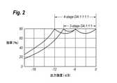
図3は3段のドハティアンプの機能ブロック図であって、キャリアアンプ100、二つのピークアンプ、101、102それぞれの出力に伝送線路TL00~TL02を挿入することにより、伝送線路の出力からそれぞれのアンプを見込んだインピーダンスをショートとする構成である。端子RFINに与えられる高周波信号は1:3の入力分配器20に入力し、同相で強度の同じ三つの出力に分岐される。入力分配器20については、たとえば、ウィルキンソン型の1:3分配器が挙げられる。そして、キャリアアンプ100に入力する信号のみ、λ/2長の伝送線路を介することで、この信号の位相を180°遅らせる。各アンプ100~102の出力は同様の構成を有する(インピーダンスZ0、線路長L0の伝送線路TL00~TL02)オフセットユニット(位相器)30を介して出力結合器40に入力する。ここでインピーダンスZ0、線路長L0は、ピークアンプ101、102がオフの時に、オフセットユニット(位相器)30の各出力からピークアンプ101、102を見込んだインピーダンスをショートとするインピーダンスZ0であり、線路長L0である。伝送線路TL00~TL02の作用、効果の詳細については後述する。キャリアアンプ100、ピークアンプ101、102とも同じ構成のアンプであるので、オフとなった時には同様の出力インピーダンス(そのドレイン端子からアンプ内部を見込んだインピーダンス)を有する。伝送線路TL00~TL02もキャリアアンプ100、ピークアンプ101、102に対して同様の構成とする。この3段の対称ドハティアンプは図2に示す様に三つの効率極値を示し、その最大バックオフは9dBcで与えられる。FIG. 3 is a functional block diagram of a three-stage Doherty amplifier, in which a transmission line TL00 to TL02 is inserted into each output ofa carrier amplifier 100, two peak amplifiers, 10 1, 102 to transmit a transmission line. It is a configuration that shorts the impedance that anticipates each amplifier from the output of. The high frequency signal given to the terminal RFIN is input to the
二つのピークアンプ101、102がオフとされる低出力域では、ノードN1からピークアンプ101、102を見込んだインピーダンスはオフセットユニット(位相器)30の出力がショートとみなせ、かつ、この疑似ショート端子にλ/4の線路長を有する伝送線路TL1、TL2が接続されているので、オープンとみなすことができる。従って、三つのアンプ100~102の出力に対する結合ノードN0からこのノードN1を見込んだインピーダンスは、それぞれがλ/4の線路長を有する二つの伝送線路TLA、TLBを介して接続されているので、これもオープンとみなすことができる。従って、ピークアンプ101、102がオフとなる低出力域では、ノードN0に対して伝送線路TLB以下の構成は何らの寄与もしない。In the low output region where the two peak amplifiers 101 and 102 are turned off, the impedance that anticipates the peak amplifiers 101 and 102 from the node N1 can be regarded as the output of the offset unit (phase device) 30 as a short circuit. Since the transmission lines TL1 and TL2 having a line length of λ / 4 are connected to this pseudo short terminal, it can be regarded as open. Therefore, the impedance expected from the coupling node N0 to the outputs of the three amplifiers100 to102 via thetwo transmission lines TLA and TLB , each of which has a line length of λ / 4. Since it is connected, this can also be considered open. Therefore, in the low output region where the peak amplifiers 101 and 102 are turned off, the configuration below the transmission line TLB does not contribute to the node N0 .
RFOUT端子が50Ωで終端されている時は(RFOUT端子に50Ωの特性インピーダンスを有する伝送線路が接続されている時)、ノードN0からこの終端を見込んだインピーダンスは、ZT2/50で与えられ、キャリアアンプ100に対するオフセットユニット(位相器)30の出力からノードN0側を見込んだインピーダンスは(Z2/ZT)2*50で与えられる。伝送線路TL00の線路長L0、そのインピーダンスZ0、及びインピーダンス比(Z2/ZT)を設定することにより、従来の2段のドハティアンプで一般的な、キャリアアンプのみが動作する低出力域で、キャリアアンプの負荷を数百Ωとすることは容易である。When the RFOUT terminal is terminated with 50Ω (when a transmission line with a characteristic impedance of 50Ω is connected to the RFOUT terminal), the impedance expected to be terminated from nodeN0 is ZT 2/50. The impedance given in1 and expected from the output of the offset unit (phase device) 30 with respect to the carrier amplifier 100 on the node N 0side is given by (Z2 / ZT ) 2 * 50. By setting the line length L0 of the transmission line TL00 , its impedance Z0 , and the impedance ratio (Z2 / ZT ), a low level at which only the carrier amplifier operates, which is common in conventional two-stage Doherty amplifiers. In the output range, it is easy to set the load of the carrier amplifier to several hundred Ω.
入力信号強度が増加し、第1のピークアンプ101も動作する最初のバックオフ領域になると、ノードN1から第2のピークアンプ102を見込むインピーダンスは依然としてオープン状態にあるが、第1のピークアンプ101を見込むインピーダンスが有意な値となる。この場合、結合ノードN0においてキャリアアンプの出力は伝送線路TL00、TLCを介して、一方第1のピークアンプ101の出力は伝送線路TL01、TL1、TLA、TLBを介して結合する。キャリアアンプ100とピークアンプ101は同一構成であるので、両アンプの生ずる信号の位相遅れは同様であり、また、二つの伝送線路TL00、TL01で生ずる位相遅れも同様である。故に、キャリアアンプ100の出力に対して第1のピークアンプ101の出力は、λ/4の伝送線路の数の差、すなわちλ/4×2=λ/2の位相差が生ずる(第1のピークアンプ101の出力が遅れる)。キャリアアンプ100の入力信号がピークアンプ101、102の入力信号に対して、伝送線路25を挿入することにより既にλ/2遅れているので、第1のピークアンプの出力は伝送線路TL1、TLA、TLBを介して結合ノードN0にキャリアアンプ100からの出力と同相で到達し、安定的に結合する。この時、第2のピークアンプ102は依然としてオフ状態にあるので、第2のピークアンプ102に対するオフセットユニット(位相器)30の出力、すなわち、伝送線路TL02の出力はショートとみなせ、ノードN1から見込んだ伝送線路TL2はオープン状態になり、第1のピークアンプ101の出力に影響をしない。When the input signal strength increases and the first peak amplifier 101 also operates in the first backoff region, the impedance expecting the second peak amplifier 102 from the node N1 is still open, but the first one. The impedance that expects the peak amplifier 101 becomes a significant value. In this case, the output of the carrier amplifier at the coupling node N0 is via the transmission lines TL00 and TLC , while the output of the first peak amplifier 101 is via the transmission lines TL01 , TL1 , TLA and TLB. And combine. Since the carrier amplifier100 and the peak amplifier101 have the same configuration, the phase delays of the signals generated by both amplifiers are the same, and the phase delays generated by the two transmission lines TL 00and TL01 are also the same. Therefore, the output of thefirst
出力がさらに増加し、第2のピークアンプ102も動作するバックオフ領域になると、第2のピークアンプ102の出力と第1のピークアンプ101の出力は、ノードN1にて同相で結合し、これは、キャリアアンプ100の出力に関するノードN0の位相とπ異なる。そして、ノードN1にて結合された二つのピークアンプ101、102の出力は、それぞれがλ/4の長さ(π/2)を有する二つの伝送線路TLA、TLBを介して、すなわち、πだけ位相を遅らせてノードN0にてキャリアアンプ100の出力と同相で結合する。When the output is further increased and the backoff region in which the second peak amplifier 102 also operates is reached, the output of the second peak amplifier 102 and the output of the first peak amplifier 101 are in phase witheach other at the node N1. Combined, this is π different from the phase of node N0 withrespect to the output of
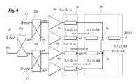
図4は4段の反転型ドハティアンプの構成を模式的に示す。端子RFINに入力したRF信号は、2段の3dBの入力カプラ20a~20cで4分岐される。入力カプラ20a~20cの一方の出力(入力と接続した出力)は、他方の出力(入力と結合した出力)に対して位相が90°遅れる。従って、4分岐されたうちの一の入力を受けるキャリアアンプ100に入力するRF信号の位相は、入力端RFINに対して180°遅れ、その強度が1/4である。ピークアンプ101に入力するRF信号は90°、ピークアンプ102に入力するRF信号は0°、ピークアンプ103に入力するRF信号は90°、それぞれ入力端RFINに対して位相遅れが生ずる。FIG. 4 schematically shows the configuration of a four-stage inversion type Doherty amplifier. The RF signal input to the terminal RFIN is branched into four by two stages of 3
キャリアアンプ100、及び各ピークアンプ10n(n=1~3)の出力はそれぞれ、オフセットユニット(位相器)30内の伝送線路TL00~TL03を介して出力結合器40に入力する。伝送線路TL00~TL03のインピーダンスZ0、線路長L0を有する。The outputs of the
出力結合器40では、キャリアアンプ100の直接の出力に対して、各ピークアンプ101~103の出力を、それぞれ伝送線路TL01~TL03を介して結合する。すなわち、ピークアンプ101の出力は伝送線路TL01を介して、第2のピークアンプ102の出力は伝送線路TL02、TL01を介して、そして、第3のピークアンプ103の出力は伝送線路TL03を介して、キャリアアンプ100の出力とノードN0にて合成される。ここで、キャリアアンプ100の入力は入力端RFINに対して180°遅れた位相を有していた。従って、結合ノードN0には180°位相遅れに加えてキャリアアンプ100での遅れ、及び伝送線路TL00による遅れを加えた位相で現れる。In the
第1のピークアンプ101については、このピークアンプ101に入力するRF信号が既に端子RFINにおける位相に対して90°遅れたものになっている。換言すると、第1のピークアンプ101の入力は、キャリアアンプ100の入力に対して90°その位相が進んでいる。そして第1のピークアンプ101の出力は、第1の伝送線路TL1を介して結合ノードN0で、キャリアアンプ100出力と合成される。伝送線路TL1はλ/4長を有しているので、この伝送線路TL1で位相が90°遅れることになる。従って、第1のピークアンプ101の出力は、入力端RFINでの位相に対して、入力段のカプラ20cで90°、伝送線路TL1で90°、そして、第1のピークアンプ101内および伝送線路TL0での遅れを生じて結合ノードN0に至る。すなわち、キャリアアンプ100の出力の位相と同位相をもって結合ノードN0にて合成さえる。Regarding thefirst peak amplifier101 , the RF signal input to the
第2のピークアンプ102に対しては、その入力RF信号は入力カプラ20a、20cでの位相遅れを伴わずに入力する。すなわち、キャリアアンプ100の入力に対して180°進んだ位相で第2のピークアンプ102に入力する。が、第2のピークアンプ102の出力は、二つの伝送線路TL2、TL1を介して結合ノードN0に至る。二つの伝送線路TL2、TL1はそれぞれλ/4の長さを有しているので、この二つの伝送線路TL2、TL1で合計180°の位相遅れが生ずる。入力端RFINに対しては、この180°の遅れに加えて、第2のピークアンプ102での遅れ、及び伝送線路TL00での遅れを加味した遅れとなる。アンプ構成、伝送線路TL00~TL03の構成は同様であるので、これらアンプと伝送線路ではキャリアアンプ100と第2のピークアンプ102の出力に位相差は実質生じない。故に、第2のピークアンプ102の出力はノードN0にて、キャリアアンプ100、第1のピークアンプ101の出力と同相で合成される。For thesecond
第3のピークアンプ103に対しては、入力カプラ20aで90°遅れた信号が入力し、第3のピークアンプ103の出力は、伝送線路TL3を介して結合ノードN0に至る。伝送線路TL3はλ/4の長さを有しているので、90°の位相遅れが生ずる。その結果、第3のピークアンプ103の出力は、キャリアアンプ100の出力に対して同位相でノードN0にて各アンプ100~102の出力と適切に結合される。A signal delayed by 90 ° is input to the third peak amplifier 103 , and the output of the third peak amplifier 103 reaches the coupling node N0 via the transmission line TL3 . Since the transmission line TL3 has a length of λ / 4, a phase delay of 90 ° occurs. As a result, the output of thethird peak amplifier103 is appropriately coupled with the output of each
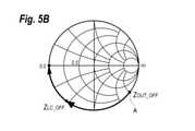
合成回路におけるインピーダンスの変化について説明する。キャリアアンプ100のみが動作する低出力領域では、ピークアンプ101~103はオフ状態にある。しかし、その出力インピーダンスが無限(∞)にあるわけではなく、たとえば、ピークアンプ101~103が単体の電界効果トランジスタ(FET)で構成されている場合には、ドレイン-ソース間の接合容量、ドレイン電極に対するボンディングワイヤの有する寄生インダクタンス、等により、その出力がオープンと見なせない場合がほとんどである。図5Aはキャリアアンプ100、ピークアンプ101~103のドレイン側を模式的に示した回路図であり、図5Bはその時のスミスチャートを示す。The change in impedance in the synthesis circuit will be described. In the low output region where only the
各アンプが含むFETのドレイン負荷にはドレイン-ソース間の接合容量が、ドレイン電極を引き出すためのボンディングワイヤに起因する寄生インダクタンスが必然的に存在する。この時、FETの電極からFET内部を見込んだインピーダンスをZOUT_OFFとすると、これはスミスチャート上では、たとえば、図5Bの点Aに相当する。FETのドレイン出力には、キャパシタC、インダクタLで構成される整合回路が挿入されている。図4における容量CはFETのドレインとグランドとの間に接続された容量で寄生成分ではない。また、インダクタLは、この整合回路の容量Cとオフセット伝送線路を接続するボンディングワイヤに由来するインダクタンス成分を示す。このマッチング回路により、スミスチャート上の点ZOUT_OFFはチャートの外縁に沿って右回りに点ZLC_OFFまで移動する。In the drain load of the FET included in each amplifier, the junction capacitance between the drain and the source is inevitably present, and the parasitic inductance due to the bonding wire for drawing out the drain electrode is inevitably present. At this time, assuming that the impedance looking inside the FET from the electrode of the FET is ZOUT_OFF , this corresponds to, for example, the point A in FIG. 5B on the Smith chart. A matching circuit composed of a capacitor C and an inductor L is inserted in the drain output of the FET. The capacitance C in FIG. 4 is the capacitance connected between the drain and the ground of the FET and is not a parasitic component. Further, the inductor L shows an inductance component derived from the bonding wire connecting the capacitance C of the matching circuit and the offset transmission line. By this matching circuit, the point ZOUT_OFF on the Smith chart moves clockwise along the outer edge of the chart to the point ZLC_OFF .
オフセットユニット(位相器)30に含まれる伝送線路TL00~TL03はこの点ZLC_OFFを左端のショート(0Ω)にまで移動させる長さを有する。点ZLC_OFFがチャット上の縁に存在しているので、オフセット伝送線路TL00~TL03のインピーダンスはZ0、その伝送路長L0が点ZLC_OFFから左端(Z=0)までに相当する。なぜならば、スミスチャート上で右端の点から右回りに左端の点までの距離がλ/4に相当するので、図6の例では、伝送線路TL00~TL03はほぼλ/16の長さを有するものである。The transmission lines TL00 to TL03 included in the offset unit (phase detector) 30 have a length that moves this point ZLC_OFF to the leftmost short (0Ω). Since the point ZLC_OFF exists at the edge on the chat, the impedance of the offset transmission lines TL00 to TL03 corresponds to Z0 , and the transmission line length L0 corresponds to the left end (Z = 0) from the point ZLC_OFF . .. This is because the distance from the rightmost point to the leftmost point clockwise on the Smith chart corresponds to λ / 4, so in the example of FIG. 6, the transmission lines TL00 to TL03 have a length of approximately λ / 16. It has.
この様にインピーダンスをLCマッチング回路及びオフセット伝送線路により変換することで、伝送線路TL00~TL03の出力端では、そのインピーダンスがショート(Z=0)と見なせることになる。したがって、伝送線路TL00~TL03の各出力端に、あらためて線路長λ/4の伝送線路TL1~TL3を接続すると、その負荷側の出力端では各アンプがオフの時に理想的にオープンと見なすことが可能となる。By converting the impedance by the LC matching circuit and the offset transmission line in this way, the impedance can be regarded as a short circuit (Z = 0) at the output ends of the transmission lines TL00 to TL03 . Therefore, if transmission lines TL1 to TL3 having a line length of λ / 4 are connected to the output ends of the transmission lines TL00 to TL03 , the output ends on the load side are ideally opened when each amplifier is off. Can be regarded as.
全てのアンプ100~103がその飽和動作を行う最大出力時について考える。また、出力端子RFOUTにはその負荷として50Ωのインピーダンスが接続されているとする。最大出力時には、全てのアンプ100~103の出力インピーダンスは50Ωに整合されるので、結合ノードN0における合成インピーダンスは12.5Ωとなる。出力伝送線路TLTによりこの合成インピーダンス12.5Ωが50Ωに変換されるので、出力伝送線路のインピーダンスは25Ωとなる。Consider the maximum output at which all amplifiers100 to103 perform their saturation operation. Further, it is assumed that an impedance of 50Ω is connected to the output terminal RFOUT as a load thereof. At the maximum output, the output impedances of all
キャリアアンプ100のみが動作する低出力領域では、キャリアアンプ100の出力インピーダンスは12.5Ωとなる様に、LCマッチング回路の定数が設定される。すなわち、その出力端インピーダンス12.5Ωと、キャリアアンプ100の出力インピーダンスZOUT_ONとの間のインピーダンス変換をLCマッチング回路により行う。同様に、キャリアアンプ100と第1のピークアンプ101が飽和出力動作をし、他の二つのピークアンプ102、103がオフされている時には、キャリアアンプ100についてのオフセット伝送線路TL00の出力端、および第1のピークアンプ101についてオフセット伝送線路TL01の出力端のインピーダンスがともに25Ωに設定される様に、LCマッチング回路の定数が設定される。キャリアアンプ100と二つのピークアンプ101、102が飽和動作する時も同様に考えることができる。In the low output region where only the
図6は、図4に示す4段の反転ドハティアンプのRFOUT端子における強度とその時観測された効率を示したものである。-12dBcのバックオフは出力電流50dBmで得られ、その時の効率は60%を超えている。出力が50dBmまではキャリアアンプ100のみが動作し、50dBm~62dBmの間でピークアンプ101~103が順次動作を開始する。また、その時の実質的な効率の低下は観測されていない。FIG. 6 shows the intensity at the RFOUT terminal of the four-stage inverting Doherty amplifier shown in FIG. 4 and the efficiency observed at that time. A backoff of -12 dBc is obtained with an output current of 50 dBm, at which time the efficiency is over 60%. Only the
100:キャリアアンプ、101~103:ピークアンプ、20:入力分配器、20a~20c:入力カプラ、ZT:終端抵抗、30:オフセットユニット(位相器)、TL00~TL03;オフセット伝送線路、TLA~TLC、TL1~TL3:合成伝送線路、TLT:出力伝送線路、40:出力結合器。100: Carrier amplifier, 10 1to 103 : Peak amplifier, 20: Input distributor, 20a to 20c: Input coupler, ZT : Termination resistor, 30: Offset unit (phase device), TL00 to TL03 ; Offset Transmission line, TLA to TLC , TL1 to TL3 : Composite transmission line, TLT : Output transmission line, 40: Output combiner.
Claims (4)
Translated fromJapanese入力信号を前記キャリアアンプと前記第1~第3のピークアンプに等しく分配する入力分配器と、
前記キャリアアンプと前記第1~第3のピークアンプを含むアンプユニットと、
前記キャリアアンプの出力に接続されたキャリアオフセット伝送線路と、前記第1~第3のピークアンプそれぞれの出力に接続された第1~第3のオフセット伝送線路を有するオフセットユニットと、
前記キャリアオフセット伝送線路および前記第1~第3のオフセット伝送線路の出力を複数の結合伝送線路を介して結合する出力結合器と、を備え、
前記キャリアオフセット伝送線路および前記第1~第3のオフセット伝送線路は、前記キャリアアンプ及び前記第1~第3のピークアンプがオフされている時の出力インピーダンスをショート状態に変換する伝送線路であり、
前記出力結合器は結合ノードを含み、前記キャリアオフセット伝送線路の出力は直接に、前記第1のピークアンプの出力に接続した前記第1のオフセット伝送線路の出力は第1の結合伝送線路を介して、前記第2のピークアンプの出力に接続した前記第2のオフセット伝送線路の出力は、第2の結合伝送線路及び前記第1の結合伝送線路を介して、前記第3のピークアンプの出力に接続した前記第3のオフセット伝送線路の出力は第3の結合伝送線路を介して、それぞれ前記結合ノードに接続する、
ドハティアンプ。A Doherty amplifier equipped withone carrier amplifier andfirst to third peak amplifiers.
An input distributor that equally distributes the input signal tothe carrier amplifier andthe first to third peak amplifiers.
An amplifier unit includingthe carrier amplifier andthe first to third peak amplifiers,
A carrier offset transmission line connected to the output of thecarrier amplifier, an offset unit havingfirst to third offset transmission lines connected to the outputs ofthe first to third peak amplifiers, and an offset unit.
The carrier offset transmission line and the output coupler for coupling the outputs of the first to third offset transmission lines via a plurality of coupled transmission lines are provided.
The carrier offset transmission line and the first to third offset transmission lines are transmission lines that convert the output impedance whenthe carrier amplifier andthe first to third peak amplifiers are off into a short state.Ri ,
The output combiner includes a coupling node, the output of the carrier offset transmission line is directly connected to the output of the first peak amplifier, and the output of the first offset transmission line is via the first coupled transmission line. The output of the second offset transmission line connected to the output of the second peak amplifier is the output of the third peak amplifier via the second coupled transmission line and the first coupled transmission line. The output of the third offset transmission line connected to the third offset transmission line is connected to the combined node via the third combined transmission line.
Doherty amp.
前記第1の結合伝送線路は、λ/4の線路長を有し、かつ、負荷インピーダンスの1/2のインピーダンスを有する、請求項1に記載のドハティアンプ。The carrier offset transmission line,the first to third offset transmission lines,and the second and third coupled transmission lines have a line length of λ / 4, and the impedance is equal to the load impedance.
The Doherty amplifier according to claim1 ,wherein the first coupled transmission line has a line length of λ / 4 and an impedance of 1/2 of the load impedance.
Applications Claiming Priority (2)
| Application Number | Priority Date | Filing Date | Title |
|---|---|---|---|
| US201662427931P | 2016-11-30 | 2016-11-30 | |
| US62/427,931 | 2016-11-30 |
Publications (2)
| Publication Number | Publication Date |
|---|---|
| JP2018093490A JP2018093490A (en) | 2018-06-14 |
| JP7009711B2true JP7009711B2 (en) | 2022-01-26 |
Family
ID=62191114
Family Applications (1)
| Application Number | Title | Priority Date | Filing Date |
|---|---|---|---|
| JP2017230714AActiveJP7009711B2 (en) | 2016-11-30 | 2017-11-30 | Doherty amp |
Country Status (3)
| Country | Link |
|---|---|
| US (1) | US10187015B2 (en) |
| JP (1) | JP7009711B2 (en) |
| CN (1) | CN108123690B (en) |
Families Citing this family (5)
| Publication number | Priority date | Publication date | Assignee | Title |
|---|---|---|---|---|
| CN109327191B (en)* | 2017-07-31 | 2023-10-24 | 安普林荷兰有限公司 | Four-way doherty amplifier and mobile communication base station |
| US10601375B2 (en)* | 2017-10-03 | 2020-03-24 | Sumitomo Electronic Devices Innovations, Inc. | Modified three-stage doherty amplifier |
| CN109660214A (en)* | 2018-12-20 | 2019-04-19 | 佛山臻智微芯科技有限公司 | One kind being applied to the 5th third-generation mobile communication base station Doherty power amplifier |
| CN113517862A (en)* | 2020-04-10 | 2021-10-19 | 华为技术有限公司 | Signal processing method and device |
| WO2025192166A1 (en)* | 2024-03-15 | 2025-09-18 | 株式会社村田製作所 | Transmission circuit and communication apparatus equipped with same |
Citations (1)
| Publication number | Priority date | Publication date | Assignee | Title |
|---|---|---|---|---|
| JP2007535828A (en) | 2003-03-28 | 2007-12-06 | アンドリュー・コーポレーション | High efficiency amplifier and design method thereof |
Family Cites Families (17)
| Publication number | Priority date | Publication date | Assignee | Title |
|---|---|---|---|---|
| US5568086A (en)* | 1995-05-25 | 1996-10-22 | Motorola, Inc. | Linear power amplifier for high efficiency multi-carrier performance |
| US6791417B2 (en)* | 2002-01-28 | 2004-09-14 | Cree Microwave, Inc. | N-way RF power amplifier circuit with increased back-off capability and power added efficiency using selected phase lengths and output impedances |
| US6812786B2 (en)* | 2002-04-11 | 2004-11-02 | Andrew Corporation | Zero-bias bypass switching circuit using mismatched 90 degrees hybrid |
| KR20060077818A (en)* | 2004-12-31 | 2006-07-05 | 학교법인 포항공과대학교 | Power amplification device using asymmetric power drive |
| KR101484796B1 (en) | 2007-04-23 | 2015-01-20 | 달리 시스템즈 씨오. 엘티디. | N-way doherty distributed power amplifier |
| EP2159912A1 (en)* | 2008-08-29 | 2010-03-03 | Alcatel, Lucent | Multi-band Doherty amplifier |
| JP5243192B2 (en)* | 2008-11-12 | 2013-07-24 | 株式会社日立国際電気 | amplifier |
| US8115546B2 (en)* | 2009-05-15 | 2012-02-14 | Samsung Electronics Co., Ltd. | Apparatus and method for maximizing performance of peaking amplifier in doherty amplifier |
| EP2403135B1 (en) | 2010-06-24 | 2013-12-11 | Alcatel Lucent | Power amplifier for mobile telecommunications |
| US9077285B2 (en) | 2012-04-06 | 2015-07-07 | Freescale Semiconductor, Inc. | Electronic devices with multiple amplifier stages and methods of their manufacture |
| JP2014075717A (en)* | 2012-10-04 | 2014-04-24 | Fujitsu Ltd | Doherty amplifier |
| JP2014175761A (en)* | 2013-03-07 | 2014-09-22 | Japan Radio Co Ltd | Doherty power amplifier |
| EP2876810B1 (en)* | 2013-11-22 | 2016-04-13 | Samba Holdco Netherlands B.V. | Doherty Amplifier |
| EP2933918B1 (en)* | 2014-04-15 | 2017-11-22 | Ampleon Netherlands B.V. | Ultra wideband doherty amplifier |
| JP6467956B2 (en)* | 2015-02-02 | 2019-02-13 | 日本電気株式会社 | Doherty amplifier circuit with load impedance adjustment circuit |
| EP3322091B1 (en)* | 2015-02-04 | 2019-09-18 | Ampleon Netherlands B.V. | Doherty amplifier |
| CN105897182B (en)* | 2016-05-11 | 2019-03-05 | 杭州电子科技大学 | A kind of high efficiency Doherty power amplifier based on harmonic controling |
- 2017
- 2017-11-30JPJP2017230714Apatent/JP7009711B2/enactiveActive
- 2017-11-30CNCN201711237150.4Apatent/CN108123690B/enactiveActive
- 2017-11-30USUS15/827,541patent/US10187015B2/enactiveActive
Patent Citations (1)
| Publication number | Priority date | Publication date | Assignee | Title |
|---|---|---|---|---|
| JP2007535828A (en) | 2003-03-28 | 2007-12-06 | アンドリュー・コーポレーション | High efficiency amplifier and design method thereof |
Also Published As
| Publication number | Publication date |
|---|---|
| CN108123690A (en) | 2018-06-05 |
| US10187015B2 (en) | 2019-01-22 |
| US20180152149A1 (en) | 2018-05-31 |
| CN108123690B (en) | 2023-04-28 |
| JP2018093490A (en) | 2018-06-14 |
Similar Documents
| Publication | Publication Date | Title |
|---|---|---|
| JP7009711B2 (en) | Doherty amp | |
| US9899962B2 (en) | Power amplifier | |
| EP3461000B1 (en) | Doherty amplifier | |
| US10432147B2 (en) | Inverted three-stage Doherty amplifier | |
| US10340855B2 (en) | Doherty amplifier | |
| US11133781B2 (en) | Doherty amplifier and Doherty amplifier circuit | |
| WO2017008512A1 (en) | Doherty power amplifier circuit | |
| WO2009045686A2 (en) | Inverted doherty amplifier with increased off-state impedence | |
| JP2017501662A (en) | Doherty power amplifier, communication device, and system | |
| JP2018085635A (en) | Power amplifier | |
| EP3070840A1 (en) | Power amplifier and power amplification method | |
| US9112454B2 (en) | Semiconductor power amplifier | |
| WO2015180064A1 (en) | Doherty power amplifier and transmitter | |
| US20130293295A1 (en) | Compact rf power amplifier | |
| US10418947B2 (en) | Doherty amplifier | |
| JP6565231B2 (en) | Distributed amplifier | |
| JP6273741B2 (en) | Power amplifier and control method using power amplifier | |
| JP5390495B2 (en) | High frequency amplifier | |
| WO2016149904A1 (en) | Power amplifying equipment | |
| CN107911084A (en) | A kind of power amplifier | |
| KR101901510B1 (en) | Power Amplifier Using Equivalent Transformer | |
| JP6056515B2 (en) | Power amplifier module | |
| JP2007150377A (en) | Distributor, combiner and power amplifier using them |
Legal Events
| Date | Code | Title | Description |
|---|---|---|---|
| A625 | Written request for application examination (by other person) | Free format text:JAPANESE INTERMEDIATE CODE: A625 Effective date:20200721 | |
| A977 | Report on retrieval | Free format text:JAPANESE INTERMEDIATE CODE: A971007 Effective date:20210419 | |
| A131 | Notification of reasons for refusal | Free format text:JAPANESE INTERMEDIATE CODE: A131 Effective date:20210518 | |
| A521 | Request for written amendment filed | Free format text:JAPANESE INTERMEDIATE CODE: A523 Effective date:20210719 | |
| TRDD | Decision of grant or rejection written | ||
| A01 | Written decision to grant a patent or to grant a registration (utility model) | Free format text:JAPANESE INTERMEDIATE CODE: A01 Effective date:20211214 | |
| A61 | First payment of annual fees (during grant procedure) | Free format text:JAPANESE INTERMEDIATE CODE: A61 Effective date:20211222 | |
| R150 | Certificate of patent or registration of utility model | Ref document number:7009711 Country of ref document:JP Free format text:JAPANESE INTERMEDIATE CODE: R150 | |
| R250 | Receipt of annual fees | Free format text:JAPANESE INTERMEDIATE CODE: R250 |