JP7001862B2 - Luminescent device - Google Patents
Luminescent deviceDownload PDFInfo
- Publication number
- JP7001862B2 JP7001862B2JP2021086221AJP2021086221AJP7001862B2JP 7001862 B2JP7001862 B2JP 7001862B2JP 2021086221 AJP2021086221 AJP 2021086221AJP 2021086221 AJP2021086221 AJP 2021086221AJP 7001862 B2JP7001862 B2JP 7001862B2
- Authority
- JP
- Japan
- Prior art keywords
- light emitting
- support
- emitting panel
- protective layer
- layer
- Prior art date
- Legal status (The legal status is an assumption and is not a legal conclusion. Google has not performed a legal analysis and makes no representation as to the accuracy of the status listed.)
- Active
Links
Images


Classifications
- H—ELECTRICITY
- H05—ELECTRIC TECHNIQUES NOT OTHERWISE PROVIDED FOR
- H05B—ELECTRIC HEATING; ELECTRIC LIGHT SOURCES NOT OTHERWISE PROVIDED FOR; CIRCUIT ARRANGEMENTS FOR ELECTRIC LIGHT SOURCES, IN GENERAL
- H05B33/00—Electroluminescent light sources
- H05B33/02—Details
- F—MECHANICAL ENGINEERING; LIGHTING; HEATING; WEAPONS; BLASTING
- F21—LIGHTING
- F21V—FUNCTIONAL FEATURES OR DETAILS OF LIGHTING DEVICES OR SYSTEMS THEREOF; STRUCTURAL COMBINATIONS OF LIGHTING DEVICES WITH OTHER ARTICLES, NOT OTHERWISE PROVIDED FOR
- F21V15/00—Protecting lighting devices from damage
- F21V15/01—Housings, e.g. material or assembling of housing parts
- F21V15/012—Housings with variable shape or dimensions, e.g. by means of elastically deformable materials or by movement of parts forming telescopic extensions of the housing body
- H—ELECTRICITY
- H04—ELECTRIC COMMUNICATION TECHNIQUE
- H04W—WIRELESS COMMUNICATION NETWORKS
- H04W72/00—Local resource management
- H04W72/20—Control channels or signalling for resource management
- H04W72/23—Control channels or signalling for resource management in the downlink direction of a wireless link, i.e. towards a terminal
- H—ELECTRICITY
- H04—ELECTRIC COMMUNICATION TECHNIQUE
- H04W—WIRELESS COMMUNICATION NETWORKS
- H04W72/00—Local resource management
- H04W72/50—Allocation or scheduling criteria for wireless resources
- H04W72/56—Allocation or scheduling criteria for wireless resources based on priority criteria
- H04W72/566—Allocation or scheduling criteria for wireless resources based on priority criteria of the information or information source or recipient
- H04W72/569—Allocation or scheduling criteria for wireless resources based on priority criteria of the information or information source or recipient of the traffic information
- H—ELECTRICITY
- H05—ELECTRIC TECHNIQUES NOT OTHERWISE PROVIDED FOR
- H05B—ELECTRIC HEATING; ELECTRIC LIGHT SOURCES NOT OTHERWISE PROVIDED FOR; CIRCUIT ARRANGEMENTS FOR ELECTRIC LIGHT SOURCES, IN GENERAL
- H05B33/00—Electroluminescent light sources
- H05B33/12—Light sources with substantially two-dimensional radiating surfaces
- H—ELECTRICITY
- H10—SEMICONDUCTOR DEVICES; ELECTRIC SOLID-STATE DEVICES NOT OTHERWISE PROVIDED FOR
- H10K—ORGANIC ELECTRIC SOLID-STATE DEVICES
- H10K50/00—Organic light-emitting devices
- H10K50/10—OLEDs or polymer light-emitting diodes [PLED]
- H10K50/19—Tandem OLEDs
- H—ELECTRICITY
- H10—SEMICONDUCTOR DEVICES; ELECTRIC SOLID-STATE DEVICES NOT OTHERWISE PROVIDED FOR
- H10K—ORGANIC ELECTRIC SOLID-STATE DEVICES
- H10K59/00—Integrated devices, or assemblies of multiple devices, comprising at least one organic light-emitting element covered by group H10K50/00
- H10K59/90—Assemblies of multiple devices comprising at least one organic light-emitting element
- F—MECHANICAL ENGINEERING; LIGHTING; HEATING; WEAPONS; BLASTING
- F21—LIGHTING
- F21Y—INDEXING SCHEME ASSOCIATED WITH SUBCLASSES F21K, F21L, F21S and F21V, RELATING TO THE FORM OR THE KIND OF THE LIGHT SOURCES OR OF THE COLOUR OF THE LIGHT EMITTED
- F21Y2105/00—Planar light sources
- F—MECHANICAL ENGINEERING; LIGHTING; HEATING; WEAPONS; BLASTING
- F21—LIGHTING
- F21Y—INDEXING SCHEME ASSOCIATED WITH SUBCLASSES F21K, F21L, F21S and F21V, RELATING TO THE FORM OR THE KIND OF THE LIGHT SOURCES OR OF THE COLOUR OF THE LIGHT EMITTED
- F21Y2115/00—Light-generating elements of semiconductor light sources
- F21Y2115/10—Light-emitting diodes [LED]
- F—MECHANICAL ENGINEERING; LIGHTING; HEATING; WEAPONS; BLASTING
- F21—LIGHTING
- F21Y—INDEXING SCHEME ASSOCIATED WITH SUBCLASSES F21K, F21L, F21S and F21V, RELATING TO THE FORM OR THE KIND OF THE LIGHT SOURCES OR OF THE COLOUR OF THE LIGHT EMITTED
- F21Y2115/00—Light-generating elements of semiconductor light sources
- F21Y2115/20—Electroluminescent [EL] light sources
- H—ELECTRICITY
- H10—SEMICONDUCTOR DEVICES; ELECTRIC SOLID-STATE DEVICES NOT OTHERWISE PROVIDED FOR
- H10K—ORGANIC ELECTRIC SOLID-STATE DEVICES
- H10K2102/00—Constructional details relating to the organic devices covered by this subclass
- H10K2102/301—Details of OLEDs
- H10K2102/302—Details of OLEDs of OLED structures
- H10K2102/3023—Direction of light emission
- H10K2102/3026—Top emission
- H—ELECTRICITY
- H10—SEMICONDUCTOR DEVICES; ELECTRIC SOLID-STATE DEVICES NOT OTHERWISE PROVIDED FOR
- H10K—ORGANIC ELECTRIC SOLID-STATE DEVICES
- H10K2102/00—Constructional details relating to the organic devices covered by this subclass
- H10K2102/301—Details of OLEDs
- H10K2102/311—Flexible OLED
- H—ELECTRICITY
- H10—SEMICONDUCTOR DEVICES; ELECTRIC SOLID-STATE DEVICES NOT OTHERWISE PROVIDED FOR
- H10K—ORGANIC ELECTRIC SOLID-STATE DEVICES
- H10K59/00—Integrated devices, or assemblies of multiple devices, comprising at least one organic light-emitting element covered by group H10K50/00
- H10K59/10—OLED displays
- H10K59/12—Active-matrix OLED [AMOLED] displays
- H10K59/1201—Manufacture or treatment
- H—ELECTRICITY
- H10—SEMICONDUCTOR DEVICES; ELECTRIC SOLID-STATE DEVICES NOT OTHERWISE PROVIDED FOR
- H10K—ORGANIC ELECTRIC SOLID-STATE DEVICES
- H10K59/00—Integrated devices, or assemblies of multiple devices, comprising at least one organic light-emitting element covered by group H10K50/00
- H10K59/10—OLED displays
- H10K59/12—Active-matrix OLED [AMOLED] displays
- H10K59/121—Active-matrix OLED [AMOLED] displays characterised by the geometry or disposition of pixel elements
- H10K59/1213—Active-matrix OLED [AMOLED] displays characterised by the geometry or disposition of pixel elements the pixel elements being TFTs
- H—ELECTRICITY
- H10—SEMICONDUCTOR DEVICES; ELECTRIC SOLID-STATE DEVICES NOT OTHERWISE PROVIDED FOR
- H10K—ORGANIC ELECTRIC SOLID-STATE DEVICES
- H10K59/00—Integrated devices, or assemblies of multiple devices, comprising at least one organic light-emitting element covered by group H10K50/00
- H10K59/40—OLEDs integrated with touch screens
- Y—GENERAL TAGGING OF NEW TECHNOLOGICAL DEVELOPMENTS; GENERAL TAGGING OF CROSS-SECTIONAL TECHNOLOGIES SPANNING OVER SEVERAL SECTIONS OF THE IPC; TECHNICAL SUBJECTS COVERED BY FORMER USPC CROSS-REFERENCE ART COLLECTIONS [XRACs] AND DIGESTS
- Y02—TECHNOLOGIES OR APPLICATIONS FOR MITIGATION OR ADAPTATION AGAINST CLIMATE CHANGE
- Y02E—REDUCTION OF GREENHOUSE GAS [GHG] EMISSIONS, RELATED TO ENERGY GENERATION, TRANSMISSION OR DISTRIBUTION
- Y02E10/00—Energy generation through renewable energy sources
- Y02E10/50—Photovoltaic [PV] energy
- Y02E10/549—Organic PV cells
Landscapes
- Engineering & Computer Science (AREA)
- General Engineering & Computer Science (AREA)
- Computer Networks & Wireless Communication (AREA)
- Signal Processing (AREA)
- Physics & Mathematics (AREA)
- Optics & Photonics (AREA)
- Manufacturing & Machinery (AREA)
- Microelectronics & Electronic Packaging (AREA)
- Electroluminescent Light Sources (AREA)
- Devices For Indicating Variable Information By Combining Individual Elements (AREA)
- Planar Illumination Modules (AREA)
- Fastening Of Light Sources Or Lamp Holders (AREA)
- Thin Film Transistor (AREA)
- Non-Portable Lighting Devices Or Systems Thereof (AREA)
- Illuminated Signs And Luminous Advertising (AREA)
- Surgical Instruments (AREA)
- Led Device Packages (AREA)
- Led Devices (AREA)
Description
Translated fromJapanese本発明は、発光装置、表示装置、電子機器、照明装置、又はそれらの作製方法に関する。
特に、エレクトロルミネッセンス(Electroluminescence、以下EL
とも記す)現象を利用した発光装置、表示装置、電子機器、照明装置、又はそれらの作製
方法に関する。The present invention relates to a light emitting device, a display device, an electronic device, a lighting device, or a method for manufacturing the same.
In particular, electroluminescence (hereinafter referred to as EL).
(Also referred to as) The present invention relates to a light emitting device, a display device, an electronic device, a lighting device, or a method for manufacturing them using the phenomenon.
近年、発光装置や表示装置は様々な用途への応用が期待されており、多様化が求められて
いる。In recent years, light emitting devices and display devices are expected to be applied to various applications, and diversification is required.
例えば、携帯機器用途等の発光装置や表示装置では、薄型であること、軽量であること、
又は破損しにくいこと等が求められている。For example, light emitting devices and display devices for mobile device applications are thin and lightweight.
Or, it is required that it is not easily damaged.
EL現象を利用した発光素子(EL素子とも記す)は、薄型軽量化が容易である、入力信
号に対し高速に応答可能である、直流低電圧電源を用いて駆動可能である等の特徴を有し
、発光装置や表示装置への応用が検討されている。A light emitting element using the EL phenomenon (also referred to as an EL element) has features such as being easy to be thin and lightweight, being able to respond to an input signal at high speed, and being able to be driven by using a DC low voltage power supply. However, application to light emitting devices and display devices is being studied.
例えば、特許文献1に、フィルム基板上に、スイッチング素子であるトランジスタや有機
EL素子を備えたフレキシブルなアクティブマトリクス型の発光装置が開示されている。For example,
例えば、可搬性を高めるために表示装置を小型化することで表示領域が狭くなると、一度
に表示できる情報量が減少し、一覧性が低下する。For example, if the display area is narrowed by downsizing the display device in order to improve portability, the amount of information that can be displayed at one time is reduced, and the listability is deteriorated.
本発明の一態様は、可搬性に優れた発光装置、表示装置、電子機器、もしくは照明装置を
提供することを目的の一とする。または、本発明の一態様は、一覧性に優れた発光装置、
表示装置、もしくは電子機器を提供することを目的の一とする。本発明の一態様は、可搬
性及び一覧性に優れた発光装置、表示装置、もしくは電子機器を提供することを目的の一
とする。One aspect of the present invention is to provide a light emitting device, a display device, an electronic device, or a lighting device having excellent portability. Alternatively, one aspect of the present invention is a light emitting device having excellent listability.
One of the purposes is to provide a display device or an electronic device. One aspect of the present invention is to provide a light emitting device, a display device, or an electronic device having excellent portability and listability.
本発明の一態様は、新規な発光装置、表示装置、電子機器、もしくは照明装置を提供する
ことを目的の一とする。または、本発明の一態様は、軽量な発光装置、表示装置、電子機
器、もしくは照明装置を提供することを目的の一とする。または、本発明の一態様は、信
頼性が高い発光装置、表示装置、電子機器、もしくは照明装置を提供することを目的の一
とする。または、本発明の一態様は、破損しにくい発光装置、表示装置、電子機器、もし
くは照明装置を提供することを目的の一とする。または、本発明の一態様は、厚さが薄い
発光装置、表示装置、電子機器、もしくは照明装置を提供することを目的の一とする。ま
たは、本発明の一態様は、可撓性を有する発光装置、表示装置、電子機器、もしくは照明
装置を提供することを目的の一とする。または、本発明の一態様は、継ぎ目のない広い発
光領域を有する発光装置もしくは照明装置、又は継ぎ目のない広い表示領域を有する表示
装置もしくは電子機器を提供することを目的の一とする。または、本発明の一態様は、消
費電力が低い発光装置、表示装置、電子機器、もしくは照明装置を提供することを目的の
一とする。One aspect of the present invention is to provide a novel light emitting device, display device, electronic device, or lighting device. Alternatively, one aspect of the present invention is to provide a lightweight light emitting device, display device, electronic device, or lighting device. Alternatively, one aspect of the present invention is to provide a highly reliable light emitting device, display device, electronic device, or lighting device. Alternatively, one aspect of the present invention is to provide a light emitting device, a display device, an electronic device, or a lighting device that is not easily damaged. Alternatively, one aspect of the present invention is to provide a light emitting device, a display device, an electronic device, or a lighting device having a thin thickness. Alternatively, one aspect of the present invention is intended to provide a flexible light emitting device, display device, electronic device, or lighting device. Alternatively, one aspect of the present invention is to provide a light emitting device or a lighting device having a wide seamless light emitting area, or a display device or an electronic device having a wide seamless display area. Alternatively, one aspect of the present invention is to provide a light emitting device, a display device, an electronic device, or a lighting device having low power consumption.
なお、本発明の一態様は、これらの課題の全てを解決する必要はないものとする。It should be noted that one aspect of the present invention does not need to solve all of these problems.
本発明の一態様の発光装置は、帯状の可撓性の高い領域と帯状の可撓性の低い領域とを交
互に有する。該発光装置は、可撓性の高い領域で曲げることで、折りたたむことができる
。本発明の一態様の発光装置は、折りたたんだ状態では可搬性に優れ、展開した状態では
、継ぎ目のない広い発光領域により一覧性に優れる。本発明の一態様を適用することで、
発光領域又は表示領域の広さを減らすことなく、装置の可搬性を高めることができる。The light emitting device of one aspect of the present invention alternately has strip-shaped high-flexibility regions and strip-shaped low-flexibility regions. The light emitting device can be folded by bending in a highly flexible region. The light emitting device of one aspect of the present invention is excellent in portability in the folded state, and is excellent in listability due to the wide seamless light emitting area in the unfolded state. By applying one aspect of the invention
The portability of the device can be increased without reducing the size of the light emitting area or the display area.
具体的には、本発明の一態様は、可撓性を有する発光パネルと、該発光パネルを支持し、
互いに離間する複数の支持パネルと、を有し、該支持パネルは、該発光パネルに比べて可
撓性が低い発光装置である。Specifically, one embodiment of the present invention supports a flexible light emitting panel and the light emitting panel.
It has a plurality of support panels that are separated from each other, and the support panel is a light emitting device having a lower flexibility than the light emitting panel.
また、本発明の一態様は、第1の方向に帯状の可撓性の高い領域と帯状の可撓性の低い領
域とを交互に有する発光装置であり、可撓性の高い領域は、可撓性を有する発光パネルを
有し、可撓性の低い領域は、発光パネルに比べて可撓性の低い支持パネルと、発光パネル
と、を重ねて有する発光装置である。Further, one aspect of the present invention is a light emitting device having alternating strip-shaped high-flexibility regions and strip-shaped low-flexibility regions in the first direction, and the highly flexible regions are acceptable. A light emitting device having a light emitting panel having flexibility and having a low flexibility region is a light emitting device having a support panel having a low flexibility as compared with the light emitting panel and a light emitting panel.
上記構成の発光装置において、支持パネルに比べて可撓性の高い保護層を有し、可撓性の
高い領域及び可撓性の低い領域は、発光パネルと、保護層と、を重ねて有することが好ま
しい。In the light emitting device having the above configuration, the protective layer having higher flexibility than the support panel is provided, and the highly flexible region and the less flexible region have the light emitting panel and the protective layer in an overlapping manner. Is preferable.
また、本発明の一態様は、第1の方向に帯状の可撓性の高い領域と帯状の可撓性の低い領
域とを交互に有する発光装置であり、可撓性の高い領域は、可撓性を有する発光パネルを
有し、可撓性の低い領域は、発光パネルに比べて可撓性が低い支持パネルと、支持パネル
の間の発光パネルと、を有する発光装置である。Further, one aspect of the present invention is a light emitting device having alternating strip-shaped high-flexibility regions and strip-shaped low-flexibility regions in the first direction, and the highly flexible regions are acceptable. A light emitting device having a light emitting panel having flexibility and having a low flexibility region is a support panel having a support panel having a lower flexibility than the light emitting panel and a light emitting panel between the support panels.
上記構成の発光装置において、一対の保護層を有し、保護層は、支持パネルに比べて可撓
性が高く、可撓性の低い領域では、一対の保護層が支持パネルの間に位置し、発光パネル
が一対の保護層の間に位置することが好ましい。The light emitting device having the above configuration has a pair of protective layers, the protective layer is more flexible than the support panel, and in a region of low flexibility, the pair of protective layers are located between the support panels. , The light emitting panel is preferably located between the pair of protective layers.
また、本発明の一態様は、第1の方向に帯状の可撓性の高い領域と帯状の可撓性の低い領
域とを交互に有する発光装置であり、可撓性の高い領域は、可撓性を有する発光パネルを
有し、可撓性の低い領域は、一対の支持パネルと、一対の支持パネルの間の発光パネルと
を有し、支持パネルは、発光パネルに比べて可撓性が低い発光装置である。Further, one aspect of the present invention is a light emitting device having alternating strip-shaped high-flexibility regions and strip-shaped low-flexibility regions in the first direction, and the highly flexible regions are acceptable. It has a light emitting panel with flexibility, the less flexible region has a pair of support panels and a light emitting panel between the pair of support panels, the support panel is more flexible than the light emitting panel. Is a low light emitting device.
上記構成の発光装置において、一対の保護層を有し、保護層は、支持パネルに比べて可撓
性が高く、可撓性の低い領域では、一対の保護層が一対の支持パネルの間に位置し、発光
パネルが一対の保護層の間に位置することが好ましい。In the light emitting device having the above configuration, the light emitting device has a pair of protective layers, and the protective layer is more flexible than the support panel, and in a region where the flexibility is low, the pair of protective layers are placed between the pair of support panels. It is preferably located and the light emitting panel is preferably located between the pair of protective layers.
また、上記各構成の発光装置において、連続する2つの可撓性の高い領域の一方を内曲げ
し、他方を外曲げしたとき、一方の可撓性の高い領域内における発光パネルの曲率半径を
半径とする円と、他方の可撓性の高い領域内における発光パネルの曲率半径を半径とする
円とは、当該発光装置を支持する平面に平行に移動することで重なることが好ましい。Further, in the light emitting device having each of the above configurations, when one of two consecutive highly flexible regions is bent inward and the other is bent outward, the radius of curvature of the light emitting panel in one of the highly flexible regions is determined. It is preferable that the circle having a radius and the circle having a radius of curvature of the light emitting panel in the other highly flexible region overlap by moving in parallel with the plane supporting the light emitting device.
なお、本明細書中では、発光パネルの発光面が内側になるように曲げる場合を「内曲げ」
、発光パネルの発光面が外側になるように曲げる場合を「外曲げ」と記す。また、発光パ
ネルや発光装置における発光面とは、発光素子からの光が取り出される面を指す。In the present specification, the case of bending so that the light emitting surface of the light emitting panel is inward is referred to as "inward bending".
, The case of bending so that the light emitting surface of the light emitting panel is on the outside is referred to as "outward bending". Further, the light emitting surface in the light emitting panel or the light emitting device refers to a surface from which light from the light emitting element is taken out.
また、上記構成の発光装置において、複数の可撓性の高い領域で内曲げと外曲げを交互に
繰り返したとき、発光パネルの当該発光装置を支持する平面に最も近い面と最も遠い面と
の間の最短距離Lが、複数の可撓性の高い領域内における発光パネルの曲率半径の和Dと
、発光パネルの厚さTとを用いて、L<2(D+T)で表されることが好ましい。Further, in the light emitting device having the above configuration, when the inward bending and the outward bending are alternately repeated in a plurality of highly flexible regions, the surface of the light emitting panel closest to the plane supporting the light emitting device and the surface farthest from the plane are used. The shortest distance L between them may be represented by L <2 (D + T) using the sum D of the radii of curvature of the light emitting panel in the plurality of highly flexible regions and the thickness T of the light emitting panel. preferable.
また、上記各構成の発光装置において、発光パネルは、外部接続電極を含み、外部接続電
極と重なる可撓性の低い領域Aの第1の方向の長さが、領域Aに最も近い可撓性の低い領
域Bの第1の方向の長さよりも長いことが好ましい。Further, in the light emitting device having each of the above configurations, the light emitting panel includes the external connection electrode, and the length of the low flexibility region A overlapping the external connection electrode in the first direction is the closest to the region A. It is preferably longer than the length of the low region B in the first direction.
また、上記各発光装置において、領域A、領域B、及び領域Aに最も遠い可撓性の低い領
域Cのうち、第1の方向の長さが最も長い領域は領域Aであり、次に長い領域は領域Cで
あることが好ましい。Further, in each of the above light emitting devices, among the region A, the region B, and the region C having the lowest flexibility farthest from the region A, the region having the longest length in the first direction is the region A, which is the next longest. The region is preferably region C.
上記各発光装置において、複数の可撓性の低い領域のうち、第1の方向の長さが最も長い
領域は、領域Aであることが好ましい。In each of the light emitting devices, the region having the longest length in the first direction among the plurality of regions having low flexibility is preferably the region A.
また、上記各構成の発光装置を用いた電子機器や照明装置も本発明の一態様である。また
、上記各構成の発光装置自体が電子機器や照明装置として機能する場合もある。Further, an electronic device or a lighting device using the light emitting device having each of the above configurations is also an aspect of the present invention. Further, the light emitting device itself having each of the above configurations may function as an electronic device or a lighting device.
なお、本明細書中における発光装置とは、発光素子を用いた表示装置を含む。また、発光
素子にコネクター、例えば異方導電性フィルム、もしくはTCP(Tape Carri
er Package)が取り付けられたモジュール、TCPの先にプリント配線板が設
けられたモジュール、又は発光素子にCOG(Chip On Glass)方式により
IC(集積回路)が直接実装されたモジュールも全て発光装置に含むものとする。さらに
、照明器具等に用いられる発光装置も含むものとする。The light emitting device in the present specification includes a display device using a light emitting element. Further, the light emitting element has a connector, for example, an anisotropic conductive film, or TCP (Tape Carri).
Modules with erPackage) attached, modules with a printed wiring board at the end of TCP, or modules with ICs (integrated circuits) directly mounted on light emitting elements by the COG (Chip On Glass) method are all light emitting devices. It shall include. Further, it shall include a light emitting device used for lighting equipment and the like.
本発明の一態様では、可搬性に優れた発光装置、表示装置、電子機器、もしくは照明装置
を提供できる。本発明の一態様では、一覧性に優れた発光装置、表示装置、もしくは電子
機器を提供できる。本発明の一態様では、可搬性及び一覧性に優れた発光装置、表示装置
、もしくは電子機器を提供できる。In one aspect of the present invention, it is possible to provide a light emitting device, a display device, an electronic device, or a lighting device having excellent portability. In one aspect of the present invention, it is possible to provide a light emitting device, a display device, or an electronic device having excellent listability. In one aspect of the present invention, it is possible to provide a light emitting device, a display device, or an electronic device having excellent portability and listability.
本発明の一態様では、新規な発光装置、表示装置、電子機器、もしくは照明装置を提供す
ることができる。または、本発明の一態様では、軽量な発光装置、表示装置、電子機器、
もしくは照明装置を提供することができる。または、本発明の一態様は、信頼性が高い発
光装置、表示装置、電子機器、もしくは照明装置を提供することができる。または、本発
明の一態様では、本発明の一態様は、破損しにくい発光装置、表示装置、電子機器、もし
くは照明装置を提供することができる。または、本発明の一態様では、厚さが薄い発光装
置、表示装置、電子機器、もしくは照明装置を提供することができる。または、本発明の
一態様では、可撓性を有する発光装置、表示装置、電子機器、もしくは照明装置を提供す
ることができる。または、本発明の一態様では、継ぎ目のない広い発光領域を有する発光
装置もしくは照明装置、又は継ぎ目のない広い表示領域を有する表示装置もしくは電子機
器を提供できる。または、本発明の一態様では、消費電力が低い発光装置、表示装置、電
子機器、もしくは照明装置を提供することができる。In one aspect of the present invention, a novel light emitting device, display device, electronic device, or lighting device can be provided. Alternatively, in one aspect of the invention, a lightweight light emitting device, display device, electronic device,
Alternatively, a lighting device can be provided. Alternatively, one aspect of the present invention can provide a highly reliable light emitting device, display device, electronic device, or lighting device. Alternatively, in one aspect of the present invention, one aspect of the present invention can provide a light emitting device, a display device, an electronic device, or a lighting device that is not easily damaged. Alternatively, in one aspect of the present invention, a light emitting device, a display device, an electronic device, or a lighting device having a thin thickness can be provided. Alternatively, in one aspect of the present invention, a flexible light emitting device, display device, electronic device, or lighting device can be provided. Alternatively, in one aspect of the present invention, it is possible to provide a light emitting device or a lighting device having a wide seamless light emitting area, or a display device or an electronic device having a wide seamless display area. Alternatively, in one aspect of the present invention, it is possible to provide a light emitting device, a display device, an electronic device, or a lighting device having low power consumption.
実施の形態について、図面を用いて詳細に説明する。但し、本発明は以下の説明に限定さ
れず、本発明の趣旨及びその範囲から逸脱することなくその形態及び詳細を様々に変更し
得ることは当業者であれば容易に理解される。従って、本発明は以下に示す実施の形態の
記載内容に限定して解釈されるものではない。The embodiments will be described in detail with reference to the drawings. However, the present invention is not limited to the following description, and it is easily understood by those skilled in the art that the form and details of the present invention can be variously changed without departing from the spirit and scope of the present invention. Therefore, the present invention is not construed as being limited to the description of the embodiments shown below.
なお、以下に説明する発明の構成において、同一部分又は同様な機能を有する部分には同
一の符号を異なる図面間で共通して用い、その繰り返しの説明は省略する。また、同様の
機能を指す場合には、ハッチパターンを同じくし、特に符号を付さない場合がある。In the configuration of the invention described below, the same reference numerals are commonly used between different drawings for the same parts or parts having similar functions, and the repeated description thereof will be omitted. Further, when referring to the same function, the hatch pattern may be the same and no particular reference numeral may be added.
また、図面等において示す各構成の、位置、大きさ、範囲などは、理解の簡単のため、実
際の位置、大きさ、範囲などを表していない場合がある。このため、開示する発明は、必
ずしも、図面等に開示された位置、大きさ、範囲などに限定されない。Further, the position, size, range, etc. of each configuration shown in the drawings and the like may not represent the actual position, size, range, etc. for the sake of easy understanding. Therefore, the disclosed invention is not necessarily limited to the position, size, range, etc. disclosed in the drawings and the like.
(実施の形態1)
本実施の形態では、本発明の一態様の発光装置について説明する。(Embodiment 1)
In this embodiment, a light emitting device according to one aspect of the present invention will be described.
本発明の一態様の発光装置は、帯状の可撓性の高い領域と帯状の可撓性の低い領域とを交
互に有する。該発光装置は、可撓性の高い領域で曲げることで、折りたたむことができる
。本発明の一態様の発光装置は、折りたたんだ状態では可搬性に優れ、展開した状態では
、継ぎ目のない広い発光領域により一覧性に優れる。The light emitting device of one aspect of the present invention alternately has strip-shaped high-flexibility regions and strip-shaped low-flexibility regions. The light emitting device can be folded by bending in a highly flexible region. The light emitting device of one aspect of the present invention is excellent in portability in the folded state, and is excellent in listability due to the wide seamless light emitting area in the unfolded state.
本発明の一態様の発光装置において、可撓性の高い領域は内曲げ、外曲げのいずれで折り
たたむこともできる。In the light emitting device of one aspect of the present invention, the highly flexible region can be folded by either inward bending or outward bending.
本発明の一態様の発光装置を使用しない際に、発光パネルの発光面が内側になるように曲
げることで、発光面にキズや汚れがつくことを抑制できる。When the light emitting device of one aspect of the present invention is not used, by bending the light emitting panel so that the light emitting surface is inside, it is possible to suppress scratches and stains on the light emitting surface.
本発明の一態様の発光装置を使用する際には、展開することで、継ぎ目のない広い発光領
域全体を用いてもよいし、発光パネルの発光面が外側になるように曲げることで、発光領
域の一部を用いてもよい。折りたたまれ、使用者にとって見えない発光領域を非発光領域
とすることで、発光装置の消費電力を抑制できる。When the light emitting device of one aspect of the present invention is used, it may be expanded to use the entire seamless light emitting region, or it may be bent so that the light emitting surface of the light emitting panel is on the outside to emit light. A part of the area may be used. By setting the light emitting region that is folded and invisible to the user as the non-light emitting region, the power consumption of the light emitting device can be suppressed.
以下では、2つの帯状の可撓性の高い領域と3つの帯状の可撓性の低い領域とを有する、
3つ折りが可能な発光装置を例に挙げて説明する。Below, it has two strips of high flexibility and three strips of low flexibility.
A light emitting device that can be folded in three will be described as an example.
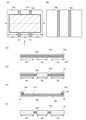
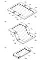
図1(A)に展開した状態の発光装置を示す。図1(B)に展開した状態又は折りたたん
だ状態の一方から他方に変化する途中の状態の発光装置を示す。図1(C)に折りたたん
だ状態の発光装置を示す。図2は、発光装置の各構成を示す斜視図である。図3(A)は
発光装置の発光面側の平面図であり、図3(B)は発光装置の発光面と対向する面側の平
面図である。図3(C)、(D)、(F)は、それぞれ図3(A)の発光装置を矢印の方
向から見た側面図の一例である。図3(E)は、図3(A)における一点鎖線A-B間の
断面図である。図4(A)、(C)、(D)は、図1(C)の発光装置を矢印の方向から
見た側面図の一例である。FIG. 1A shows a light emitting device in an expanded state. FIG. 1B shows a light emitting device in a state of being changed from one of the expanded state or the folded state to the other. FIG. 1C shows a light emitting device in a folded state. FIG. 2 is a perspective view showing each configuration of the light emitting device. FIG. 3A is a plan view of the light emitting surface side of the light emitting device, and FIG. 3B is a plan view of the surface side facing the light emitting surface of the light emitting device. 3 (C), (D), and (F) are examples of side views of the light emitting device of FIG. 3 (A) as viewed from the direction of the arrow. 3 (E) is a cross-sectional view between the alternate long and short dash lines AB in FIG. 3 (A). 4 (A), (C), and (D) are examples of side views of the light emitting device of FIG. 1 (C) as viewed from the direction of the arrow.
また、図14(A)~(C)に、それぞれ図1(A)~(C)の変形例を示す。図14(
A)に展開した状態の発光装置を示す。図14(B)に展開した状態又は折りたたんだ状
態の一方から他方に変化する途中の状態の発光装置を示す。図14(C)に折りたたんだ
状態の発光装置を示す。図15は、発光装置の各構成を示す斜視図である。図16(A)
は発光装置の発光面側の平面図であり、図16(B)は発光装置の発光面と対向する面側
の平面図である。図16(C)、(D)は、それぞれ図16(A)の発光装置を矢印の方
向から見た側面図の一例である。図16(E)は、図16(A)における一点鎖線A-B
間の断面図である。図16(F)は、図16(C)等に示す発光装置の変形例である。Further, FIGS. 14 (A) to 14 (C) show modified examples of FIGS. 1 (A) to 1 (C), respectively. FIG. 14 (
The light emitting device in the expanded state is shown in A). FIG. 14B shows a light emitting device in a state of being changed from one of the expanded state or the folded state to the other. FIG. 14C shows a light emitting device in a folded state. FIG. 15 is a perspective view showing each configuration of the light emitting device. FIG. 16 (A)
Is a plan view of the light emitting surface side of the light emitting device, and FIG. 16B is a plan view of the surface side facing the light emitting surface of the light emitting device. 16 (C) and 16 (D) are examples of side views of the light emitting device of FIG. 16 (A) as viewed from the direction of the arrow. 16 (E) shows the alternate long and short dash line AB in FIG. 16 (A).
It is a cross-sectional view between. 16 (F) is a modified example of the light emitting device shown in FIG. 16 (C) and the like.
図1(A)~(C)、図14(A)~(C)に示す発光装置は、可撓性を有する発光パネ
ル11を有する。該発光装置は、さらに複数の支持パネル15aと複数の支持パネル15
bを有する。各支持パネル15a、15bは、発光パネル11に比べて可撓性が低い。複
数の支持パネル15aは互いに離間している。複数の支持パネル15bは互いに離間して
いる。The light emitting device shown in FIGS. 1 (A) to 1 (C) and FIGS. 14 (A) to 14 (C) has a
Has b. The
図3(A)に示すように、発光装置は、可撓性の高い領域E1及び可撓性の低い領域E2
を交互に有する。可撓性の高い領域と可撓性の低い領域はそれぞれ帯状(縞状)に形成さ
れる。本実施の形態では、複数の可撓性の高い領域や複数の可撓性の低い領域が互いに平
行である例を示すが、各領域は平行に配置されていなくてもよい。As shown in FIG. 3A, the light emitting device has a highly flexible region E1 and a low flexibility region E2.
Alternately. The highly flexible region and the less flexible region are formed in strips, respectively. In the present embodiment, a plurality of highly flexible regions and a plurality of inflexible regions are shown to be parallel to each other, but the regions may not be arranged in parallel.
発光装置における可撓性の高い領域E1は、少なくとも可撓性を有する発光パネルを有し
ていればよい。特に、有機EL素子を用いた発光パネルは、高い可撓性及び耐衝撃性に加
え、薄型軽量化が図れるため、好ましい。発光パネルの構成例については実施の形態2、
3にて詳述する。The highly flexible region E1 in the light emitting device may have at least a flexible light emitting panel. In particular, a light emitting panel using an organic EL element is preferable because it is thin and lightweight in addition to high flexibility and impact resistance. The configuration example of the light emitting panel is described in the second embodiment.
It will be described in detail in 3.
発光装置における可撓性の低い領域E2は、少なくとも可撓性を有する発光パネルと、該
発光パネルに比べて可撓性の低い支持パネルとを重ねて有していればよい。The low-flexibility region E2 in the light-emitting device may have at least a light-emitting panel having flexibility and a support panel having lower flexibility than the light-emitting panel in an overlapping manner.
図16(A)に示すように、発光装置は、一方向に可撓性の高い領域及び可撓性の低い領
域を交互に有する。As shown in FIG. 16A, the light emitting device alternately has high flexibility regions and low flexibility regions in one direction.
図16(A)では、可撓性の低い領域における、可撓性の高い領域及び可撓性の低い領域
が並ぶ方向の長さを長さW1~長さW3で示す。In FIG. 16A, the lengths of the low-flexibility regions in the direction in which the high-flexibility regions and the low-flexibility regions are lined up are shown by lengths W1 to W3.
また、可撓性の低い領域には、発光パネルが有する外部接続電極を含むことが好ましい。
ここで、外部接続電極とは、例えば、図7(B)に示す導電層157等に相当する。Further, it is preferable that the region having low flexibility includes an external connection electrode included in the light emitting panel.
Here, the external connection electrode corresponds to, for example, the
図16(A)では、長さW1の可撓性の低い領域に外部接続電極を含む。発光装置では、
外部接続電極と重なる可撓性の低い領域Aの長さW1が、領域Aに最も近い可撓性の低い
領域Bの長さW3よりも長い。In FIG. 16A, the externally connected electrode is included in the low flexibility region of length W1. In the light emitting device,
The length W1 of the low flexibility region A overlapping the external connection electrode is longer than the length W3 of the low flexibility region B closest to the region A.
ここで、発光装置を折りたたんだ際に、発光パネル11の端部(折り曲げた部分、折り曲
げた状態における端部、等ともいえる)が、支持パネル15a、15bの端部よりも外側
に位置すると、発光パネル11が傷つく場合や、発光パネル11に含まれる素子が破壊さ
れる場合がある。Here, when the light emitting device is folded, the end portion of the light emitting panel 11 (which can be said to be a bent portion, an end portion in a bent state, etc.) is located outside the end portions of the
一方、図1(C)に示す折りたたんだ状態の発光装置は、発光パネル11の端部と該発光
パネル11の上下に位置する支持パネル15a、15bの端部が揃っている。これにより
、発光パネル11が傷つくこと、発光パネル11に含まれる素子が破壊されること等を抑
制できる。On the other hand, in the light emitting device in the folded state shown in FIG. 1C, the end portions of the
さらに、図14(C)に示す折りたたんだ状態の発光装置は、発光パネル11の端部が、
支持パネル15a、15bの端部よりも内側に位置する。これにより、さらに発光パネル
11が傷つくこと、発光パネル11に含まれる素子が破壊されること等を抑制できる。Further, in the light emitting device in the folded state shown in FIG. 14 (C), the end portion of the
It is located inside the ends of the
以上のことから、発光装置では、外部接続電極と重なる可撓性の低い領域Aの長さW1が
、領域Aに最も近い可撓性の低い領域Bの長さW3よりも長いことが好ましい。特に、領
域Aの長さW1、領域Bの長さW3、及び領域Aに最も遠い可撓性の低い領域Cの長さW
2のうち、長さW1が最も長く、次に長さW2が長いことが好ましい。From the above, in the light emitting device, it is preferable that the length W1 of the low flexibility region A overlapping the external connection electrode is longer than the length W3 of the low flexibility region B closest to the region A. In particular, the length W1 of the region A, the length W3 of the region B, and the length W of the region C having the lowest flexibility farthest from the region A.
Of 2, it is preferable that the length W1 is the longest and then the length W2 is the longest.
支持パネルは、発光パネルの発光面側又は発光面と対向する面側の少なくとも一方に設け
られていればよい。The support panel may be provided on at least one of the light emitting surface side of the light emitting panel or the surface side facing the light emitting surface.
図3(C)又は図16(C)に示す支持パネル15a、15bのように、発光パネルの発
光面側及び発光面と対向する面側の双方に支持パネルを有すると、一対の支持パネルによ
って発光パネルを挟持できるため、可撓性の低い領域の機械的強度を高め、発光装置がよ
り破損しにくくなり好ましい。When the support panels are provided on both the light emitting surface side and the surface side facing the light emitting surface of the light emitting panel as in the
また、支持パネル15a、15bに替えて、図3(D)又は図16(D)に示す支持パネ
ル15を用いて、支持パネル15の間に発光パネル11を配置してもよい。Further, instead of the
また、図1(A)、図2、図3(C)等では、可撓性の低い領域E2において、保護層や
発光パネルの側面が露出する例を示したが、本発明の一態様はこれに限られない。図3(
F)に示すように、可撓性の低い領域E2において、保護層や発光パネルの側面が支持パ
ネル15(又は一対の支持パネル15a、15bの一方もしくは両方)で覆われていても
よい。図21に保護層や発光パネルの側面が、支持パネル15bで覆われた発光装置の具
体的な構成を示す。図21(A)に、展開した状態の該発光装置を示す。また、図21(
B)に展開した状態又は折りたたんだ状態の一方から他方に変化する途中の状態の該発光
装置を示す。また、図21(C)に折りたたんだ状態の該発光装置を示す。また、図22
は、該発光装置の各構成を示す斜視図である。Further, in FIGS. 1 (A), 2 and 3 (C) and the like, an example in which the side surface of the protective layer or the light emitting panel is exposed in the region E2 having low flexibility is shown, but one aspect of the present invention is Not limited to this. Figure 3 (
As shown in F), in the low flexibility region E2, the side surface of the protective layer or the light emitting panel may be covered with the support panel 15 (or one or both of the pair of
B) shows the light emitting device in the state of being changed from one of the expanded state or the folded state to the other. Further, FIG. 21C shows the light emitting device in a folded state. In addition, FIG. 22
Is a perspective view showing each configuration of the light emitting device.
発光パネルの発光面側又は発光面と対向する面側のみに支持パネルを有すると、発光装置
をより薄型又はより軽量にすることができ好ましい。例えば、図16(F)に示すように
、複数の支持パネル15aを用いず、複数の支持パネル15bのみを有する発光装置とし
てもよい。It is preferable to have the support panel only on the light emitting surface side or the surface side facing the light emitting surface of the light emitting panel because the light emitting device can be made thinner or lighter. For example, as shown in FIG. 16F, a light emitting device may have only a plurality of
可撓性の高い領域E1及び可撓性の低い領域E2は、発光パネルと、支持パネルに比べて
可撓性の高い保護層と、を重ねて有することが好ましい。これにより、発光装置の可撓性
の高い領域E1が、可撓性を有し、かつ機械的強度の高い領域となり、発光装置をより破
損しにくくすることができる。したがって、可撓性の低い領域はもちろん、可撓性の高い
領域においても、発光装置が外力等による変形で壊れにくい構成にすることができる。It is preferable that the region E1 having high flexibility and the region E2 having low flexibility have a light emitting panel and a protective layer having higher flexibility as compared with the support panel in an overlapping manner. As a result, the highly flexible region E1 of the light emitting device becomes a region having flexibility and high mechanical strength, and the light emitting device can be made less likely to be damaged. Therefore, the light emitting device can be configured to be hard to break due to deformation due to an external force or the like not only in a region having low flexibility but also in a region having high flexibility.
例えば、発光パネル、支持パネル、保護層のそれぞれの厚さは、支持パネルが最も厚く、
発光パネルが最も薄い構成が好ましい。または、例えば、発光パネル、支持パネル、保護
層のそれぞれの可撓性は、支持パネルの可撓性が最も低く、発光パネルの可撓性が最も高
い構成が好ましい。このような構成とすることで、可撓性の高い領域と可撓性の低い領域
の可撓性の差が大きくなる。確実に可撓性の高い領域で折り曲げができる構成とすること
で、可撓性の低い領域で曲げが生じることを抑制でき、発光装置の信頼性を高めることが
できる。また、意図しないところで発光装置が曲がることを抑制できる。For example, the thickness of each of the light emitting panel, the support panel, and the protective layer is the thickest in the support panel.
A configuration in which the light emitting panel is the thinnest is preferable. Alternatively, for example, the flexibility of the light emitting panel, the support panel, and the protective layer is preferably such that the flexibility of the support panel is the lowest and the flexibility of the light emitting panel is the highest. With such a configuration, the difference in flexibility between the highly flexible region and the less flexible region becomes large. By making sure that the bending is possible in the region having high flexibility, it is possible to suppress the bending in the region having low flexibility, and it is possible to improve the reliability of the light emitting device. In addition, it is possible to prevent the light emitting device from bending in an unintended place.
発光パネルの発光面側及び発光面と対向する面側の双方に保護層を有すると、一対の保護
層によって発光パネルを挟持できるため、発光装置の機械的強度を高め、発光装置がより
破損しにくくなり好ましい。If the light emitting panel is provided with protective layers on both the light emitting surface side and the surface side facing the light emitting surface, the light emitting panel can be sandwiched by the pair of protective layers, so that the mechanical strength of the light emitting device is increased and the light emitting device is further damaged. It becomes difficult and preferable.
例えば、図3(C)又は図16(C)に示すように、可撓性の低い領域E2では、一対の
保護層13a、13bが一対の支持パネル15a、15bの間に位置し、発光パネル(図
示しない)が一対の保護層13a、13bの間に位置することが好ましい。For example, as shown in FIG. 3C or FIG. 16C, in the low flexibility region E2, the pair of
または、図3(D)又は図16(D)に示すように、可撓性の低い領域E2では、一対の
保護層13a、13bが支持パネル15の間に位置し、発光パネル(図示しない)が一対
の保護層13a、13bの間に位置することが好ましい。Alternatively, as shown in FIGS. 3D or 16D, in the low flexibility region E2, a pair of
発光パネルの発光面側又は発光面と対向する面側のみに保護層を有すると、発光装置をよ
り薄型又はより軽量にすることができ好ましい。例えば、保護層13aを用いず、保護層
13bのみを有する発光装置としてもよい。It is preferable to have the protective layer only on the light emitting surface side of the light emitting panel or the surface side facing the light emitting surface, because the light emitting device can be made thinner or lighter. For example, the light emitting device may have only the
また、発光パネルの発光面側の保護層13aが遮光膜であると、発光パネルの非発光領域
に外光が照射されることを抑制できる。これにより、非発光領域に含まれる駆動回路が有
するトランジスタ等の光劣化を抑制できるため好ましい。Further, when the
図2、図3(E)、図15又は図16(E)に示すように、発光パネル11の発光面側に
設けられた保護層13aの開口部は発光パネルの発光領域11aと重なる。発光領域11
aを枠状に囲う非発光領域11bと保護層13aとが重なるように設けられている。発光
パネル11の発光面と対向する面側に設けられた保護層13bは、発光領域11a及び非
発光領域11bと重なっている。保護層13bは、発光面と対向する面側により広い範囲
で、特に好ましくは該面全体に設けられることで、発光パネルをより保護することができ
、発光装置の信頼性を高めることができる。As shown in FIGS. 2, 3 (E), 15 or 16 (E), the opening of the
The non-light
本発明の一態様の発光装置において、複数の可撓性の高い領域で内曲げと外曲げを交互に
繰り返したとき、発光パネルの当該発光装置を支持する平面に最も近い面と最も遠い面と
の間の最短距離Lが、複数の可撓性の高い領域内における発光パネルの曲率半径の和Dと
、発光パネルの厚さTとを用いて、L<2(D+T)で表されることが好ましい。これに
より、発光装置の薄型化を実現できる。In the light emitting device of one aspect of the present invention, when the inward bending and the outward bending are alternately repeated in a plurality of highly flexible regions, the surface of the light emitting panel closest to the plane supporting the light emitting device and the surface farthest from the plane are used. The shortest distance L between them is represented by L <2 (D + T) using the sum D of the radii of curvature of the light emitting panel in the plurality of highly flexible regions and the thickness T of the light emitting panel. Is preferable. This makes it possible to reduce the thickness of the light emitting device.
図4(A)に示す発光装置は、1つの可撓性の高い領域を内曲げし、1つの可撓性の高い
領域を外曲げした状態である。図4(A)における保護層13aと保護層13bの境界に
発光パネルが位置するものとする。図4(A)における直径D1、直径D2を詳細に説明
する図を図4(B)に示す。直径D1は、内曲げした可撓性の高い領域における発光パネ
ルの曲率半径を半径とする円の直径を示す。直径D2は、外曲げした可撓性の高い領域に
おける発光パネルの曲率半径を半径とする円の直径を示す。発光パネル11の厚さを厚さ
Tとして示す。直径D1と直径D2の和が複数の可撓性の高い領域内における発光パネル
の曲率半径の和Dの2倍に相当するので、L<2(D+T)は、L<D1+D2+2Tと
言い換えられる。ここで、図4(A)における発光パネルの当該発光装置を支持する平面
に最も近い面と最も遠い面との間の最短距離L1は、D1+D2+3Tである。The light emitting device shown in FIG. 4A is in a state in which one highly flexible region is internally bent and one highly flexible region is outwardly bent. It is assumed that the light emitting panel is located at the boundary between the
支持パネル15a、15bの厚さや保護層13a、13bの厚さを薄くする、内曲げする
可撓性の高い領域と外曲げする可撓性の高い領域との間の可撓性の低い領域の幅を狭くす
る等により、図4(C)に示す発光パネルの当該発光装置を支持する平面に最も近い面と
最も遠い面との間の最短距離L2のように、L2<D1+D2+3T、さらにはL2<D
1+D2+2T、言い換えるとL2<2(D+T)を満たすことができる。A less flexible region between the more flexible region for inward bending and the more flexible region for outward bending, which reduces the thickness of the
It is possible to satisfy 1 + D2 + 2T, in other words, L2 <2 (D + T).
ここで、発光装置における、折り曲げによって重なった可撓性の低い領域のうち、外側に
位置する一対の領域は、発光装置を支持する平面と平行であることが好ましく、内側に位
置するその他の領域は該平面と平行でないことが好ましい。Here, in the light emitting device, among the low flexibility regions overlapped by bending, the pair of regions located on the outside are preferably parallel to the plane supporting the light emitting device, and other regions located on the inside. Is preferably not parallel to the plane.
本発明の一態様の発光装置において、連続する2つの可撓性の高い領域の一方を内曲げし
、他方を外曲げしたとき、一方の可撓性の高い領域内における発光パネルの曲率半径を半
径とする円と、他方の可撓性の高い領域内における発光パネルの曲率半径を半径とする円
とは、当該発光装置を支持する平面に平行に移動することで重なることが好ましい。これ
により、発光装置の薄型化を実現できる。In the light emitting device of one aspect of the present invention, when one of two consecutive highly flexible regions is bent inward and the other is bent outward, the radius of curvature of the light emitting panel in one of the highly flexible regions is determined. It is preferable that the circle having a radius and the circle having a radius of curvature of the light emitting panel in the other highly flexible region overlap by moving in parallel with the plane supporting the light emitting device. This makes it possible to reduce the thickness of the light emitting device.
図4(D)に示すように直径D1の円と直径D2の円とは、当該発光装置を支持する平面
に平行に移動すること(ここでは紙面左右方向に移動することに相当)で重なる。内曲げ
した可撓性の高い領域における発光パネルの曲率半径と、外曲げした可撓性の高い領域に
おける発光パネルの曲率半径とが、該2つの円の半径に相当するため、図4(D)に示す
発光装置は、薄型化が実現されているといえる。As shown in FIG. 4D, the circle having a diameter D1 and the circle having a diameter D2 overlap by moving in parallel with the plane supporting the light emitting device (here, corresponding to moving in the left-right direction of the paper surface). Since the radius of curvature of the light emitting panel in the inwardly bent highly flexible region and the radius of curvature of the light emitting panel in the outwardly bent highly flexible region correspond to the radii of the two circles, FIG. 4 (D). It can be said that the light emitting device shown in) has been made thinner.
また、図4(D)に示す発光パネルの当該発光装置を支持する平面に最も近い面と最も遠
い面との間の最短距離L3は、L3<D1+D2+3T、さらにはL3<D1+D2+2
T、言い換えるとL3<2(D+T)を満たすことができる。なお、図4(D)では、保
護層13a及び保護層13bをまとめて保護層13として示している。Further, the shortest distance L3 between the surface closest to the plane supporting the light emitting device of the light emitting panel shown in FIG. 4 (D) and the surface farthest from the plane is L3 <D1 + D2 + 3T, and further L3 <D1 + D2 + 2.
T, in other words, L3 <2 (D + T) can be satisfied. In FIG. 4D, the
保護層や支持パネルは、プラスチック、金属、合金、ゴム等を用いて形成できる。プラス
チックやゴム等を用いることで、軽量であり、破損しにくい保護層や支持パネルを得られ
るため、好ましい。例えば、保護層としてシリコーンゴム、支持パネルとしてステンレス
やアルミニウムを用いればよい。The protective layer and the support panel can be formed by using plastic, metal, alloy, rubber or the like. It is preferable to use plastic, rubber, or the like because it is lightweight and a protective layer and a support panel that are not easily damaged can be obtained. For example, silicone rubber may be used as the protective layer, and stainless steel or aluminum may be used as the support panel.
また、保護層や支持パネルに、靱性が高い材料を用いることが好ましい。これにより、耐
衝撃性に優れ、破損しにくい発光装置を実現できる。例えば、有機樹脂や、厚さの薄い金
属材料や合金材料を用いることで、軽量であり、破損しにくい発光装置を実現できる。な
お、同様の理由により、発光パネルを構成する基板にも靱性が高い材料を用いることが好
ましい。Further, it is preferable to use a material having high toughness for the protective layer and the support panel. As a result, it is possible to realize a light emitting device having excellent impact resistance and being hard to be damaged. For example, by using an organic resin, a thin metal material, or an alloy material, it is possible to realize a light emitting device that is lightweight and is not easily damaged. For the same reason, it is preferable to use a material having high toughness for the substrate constituting the light emitting panel.
発光面側に位置する保護層や支持パネルは、発光パネルの発光領域と重ならない場合には
、透光性を問わない。発光面側に位置する保護層や支持パネルが、少なくとも一部の発光
領域と重なる場合は、発光パネルからの発光を透過する材料を用いることが好ましい。発
光面と対向する面側に位置する保護層や支持パネルの透光性は問わない。The protective layer and the support panel located on the light emitting surface side are not limited to translucency as long as they do not overlap with the light emitting region of the light emitting panel. When the protective layer or the support panel located on the light emitting surface side overlaps with at least a part of the light emitting region, it is preferable to use a material that transmits light emitted from the light emitting panel. The translucency of the protective layer and the support panel located on the surface side facing the light emitting surface does not matter.
保護層、支持パネル、発光パネルのいずれか2つを接着する場合には、各種接着剤を用い
ることができ、例えば、二液混合型の樹脂などの常温で硬化する樹脂、光硬化性の樹脂、
熱硬化性の樹脂などの樹脂を用いることができる。また、シート状の接着剤を用いてもよ
い。また、保護層、支持パネル、発光パネルのいずれか2つ以上を貫通するネジや、挟持
するピン、クリップ等を用いて、発光装置の各構成を固定してもよい。When any two of the protective layer, the support panel, and the light emitting panel are bonded, various adhesives can be used. For example, a resin that cures at room temperature such as a two-component mixed resin, a photocurable resin, etc. ,
A resin such as a thermosetting resin can be used. Further, a sheet-shaped adhesive may be used. Further, each configuration of the light emitting device may be fixed by using a screw penetrating any two or more of the protective layer, the support panel, and the light emitting panel, a pin to be held, a clip, and the like.
本発明の一態様の発光装置は、1つの発光パネル(1つの発光領域)を、折り曲げられた
部分を境に2つ以上に分けて利用できる。例えば、折りたたむことで隠れた領域を非発光
とし、露出する領域のみが発光してもよい。これにより使用者が使用しない領域が消費す
る電力を削減することができる。In the light emitting device of one aspect of the present invention, one light emitting panel (one light emitting region) can be divided into two or more with a bent portion as a boundary. For example, the hidden area may be non-emission by folding, and only the exposed area may emit light. As a result, it is possible to reduce the power consumed by the area not used by the user.
本発明の一態様の発光装置は、各可撓性の高い領域が折り曲げられているか否かを判断す
るためのセンサを有していてもよい。例えばスイッチ、MEMS圧力センサまたは圧力セ
ンサ等を用いて構成することができる。The light emitting device of one aspect of the present invention may have a sensor for determining whether or not each highly flexible region is bent. For example, it can be configured by using a switch, a MEMS pressure sensor, a pressure sensor, or the like.
以上では、可撓性の高い領域を2つ有する発光装置を例に説明したが、本発明はこれに限
られない。例えば、図5(A)に示すように、少なくとも可撓性の高い領域E1を1つ有
していればよく、図5(B)又は図17(A)に示す可撓性の高い領域E1を3つ有する
4つ折りが可能な発光装置や、図5(C)又は図17(B)に示す可撓性の高い領域E1
を4つ有する5つ折りが可能な発光装置もそれぞれ本発明の一態様である。In the above, the light emitting device having two highly flexible regions has been described as an example, but the present invention is not limited to this. For example, as shown in FIG. 5 (A), it is sufficient to have at least one highly flexible region E1 and the highly flexible region E1 shown in FIG. 5 (B) or FIG. 17 (A). A light emitting device capable of folding in four, and a highly flexible region E1 shown in FIG. 5 (C) or FIG. 17 (B).
A light emitting device capable of folding in five, which has four of the above, is also one aspect of the present invention.
例えば、図17(A)に示す発光装置では、長さW1~長さW4のうち、長さW1が最も
長く、長さW2が次に長く、長さW3及び長さW4が最も短い。長さW3と長さW4は異
なる値であってもよい。For example, in the light emitting device shown in FIG. 17A, the length W1 is the longest, the length W2 is the next longest, and the length W3 and the length W4 are the shortest among the lengths W1 to W4. The length W3 and the length W4 may have different values.
また、図17(B)に示す発光装置では、長さW1~長さW5のうち、長さW1が最も長
く、長さW2が次に長く、長さW3、長さW4、及び長さW5が最も短い。長さW3、長
さW4、及び長さW5はそれぞれ異なる値であってもよい。Further, in the light emitting device shown in FIG. 17B, the length W1 is the longest, the length W2 is the next longest, the length W3, the length W4, and the length W5 among the lengths W1 to W5. Is the shortest. The length W3, the length W4, and the length W5 may have different values.
図6(A)、(B)にそれぞれ図5(C)に示す発光装置を5つ折りにした状態の一例を
示す。6 (A) and 6 (B) show an example of a state in which the light emitting device shown in FIG. 5 (C) is folded in five, respectively.
図6(A)では、発光パネルの当該発光装置を支持する平面に最も近い面と最も遠い面と
の間の最短距離L4が、複数の可撓性の高い領域内における発光パネルの曲率半径の和D
と、発光パネルの厚さTとを用いて、L4=2D+5Tで表される。なお、2D=D1+
D2+D3+D4である。In FIG. 6A, the shortest distance L4 between the surface of the light emitting panel closest to the plane supporting the light emitting device and the surface farthest from the plane is the radius of curvature of the light emitting panel in a plurality of highly flexible regions. Sum D
And L4 = 2D + 5T using the thickness T of the light emitting panel. 2D = D1 +
It is D2 + D3 + D4.
支持パネル15a、15bの厚さや保護層13a、13bの厚さを薄くする、内曲げする
可撓性の高い領域と外曲げする可撓性の高い領域との間の可撓性の低い領域の幅を狭くす
る等により、図6(B)に示す発光パネルの当該発光装置を支持する平面に最も近い面と
最も遠い面との間の最短距離L5が、複数の可撓性の高い領域内における発光パネルの曲
率半径の和Dと、発光パネルの厚さTとを用いて、L5<D1+D2+D3+D4+5T
、さらにはL5<D1+D2+D3+D4+2T、言い換えるとL5<2D+2Tを満た
すことができる。A less flexible region between the more flexible region for inward bending and the more flexible region for outward bending, which reduces the thickness of the
Further, L5 <D1 + D2 + D3 + D4 + 2T, in other words, L5 <2D + 2T can be satisfied.
また、図6(B)に示す直径D1の円と直径D2の円とは、当該発光装置を支持する平面
に平行に移動すること(ここでは紙面左右方向に移動することに相当)で重なる。また、
直径D3の円と直径D4の円も、当該発光装置を支持する平面に平行に移動することで重
なる。直径D1の円の半径と直径D2の円の半径は、連続する2つの可撓性の高い領域の
一方を内曲げし、他方を外曲げしたときに、内曲げした可撓性の高い領域における発光パ
ネルの曲率半径と、外曲げした可撓性の高い領域における発光パネルの曲率半径とに相当
しているといえるため、図6(B)に示す発光装置も、薄型化が実現されているといえる
。また、直径D3の円の半径と直径D4の円の半径からも同様のことがいえる。Further, the circle having a diameter D1 and the circle having a diameter D2 shown in FIG. 6B overlap by moving in parallel with the plane supporting the light emitting device (here, corresponding to moving in the left-right direction of the paper surface). again,
The circle with the diameter D3 and the circle with the diameter D4 also overlap by moving in parallel with the plane supporting the light emitting device. The radius of the circle of diameter D1 and the radius of the circle of diameter D2 are in the highly flexible regions that are inwardly bent when one of the two consecutive highly flexible regions is inwardly bent and the other outwardly bent. Since it can be said that the radius of curvature of the light emitting panel corresponds to the radius of curvature of the light emitting panel in the region of high flexibility that is bent outward, the light emitting device shown in FIG. 6B has also been made thinner. It can be said that. The same can be said from the radius of the circle having the diameter D3 and the radius of the circle having the diameter D4.
また、図6(B)に示すように、発光装置の最も外側に位置する一対の可撓性の低い領域
に比べて、その他の可撓性の低い領域の幅を狭くすることで、発光装置をより薄型にする
ことができる。Further, as shown in FIG. 6B, by narrowing the width of the other low-flexibility regions as compared with the pair of low-flexibility regions located on the outermost side of the light-emitting device, the light-emitting device is used. Can be made thinner.
また、発光装置を折りたたむ際に、可撓性の高い領域は、必ずしも内曲げと外曲げを交互
に行う必要はなく、例えば、図5(D)に示すように、各可撓性の高い領域を内曲げして
もよい。このような状態とすることで、持ち運びの際などに、発光装置の発光面にキズや
汚れが生じることを抑制できる。Further, when the light emitting device is folded, the highly flexible region does not necessarily have to be alternately bent inward and outward, and for example, as shown in FIG. 5D, each highly flexible region is formed. May be bent inward. In such a state, it is possible to prevent scratches and stains on the light emitting surface of the light emitting device when it is carried.
本実施の形態の発光装置では、一つの発光パネルを1回以上折りたたむことができる。こ
のとき、曲率半径は、例えば、1mm以上150mm以下とすることができる。In the light emitting device of the present embodiment, one light emitting panel can be folded once or more. At this time, the radius of curvature can be, for example, 1 mm or more and 150 mm or less.
本実施の形態は、他の実施の形態と適宜組み合わせることができる。This embodiment can be appropriately combined with other embodiments.
(実施の形態2)
本実施の形態では、発光パネルについて図7~図12を用いて説明する。本実施の形態で
例示する発光パネルを曲げた際、発光パネルにおける曲率半径の最小値は、1mm以上1
50mm以下、1mm以上100mm以下、1mm以上50mm以下、1mm以上10m
m以下、又は2mm以上5mm以下とすることができる。本実施の形態の発光パネルは、
小さな曲率半径(例えば2mm以上5mm以下)で折り曲げても素子が壊れることがなく
、信頼性が高い。発光パネルを小さな曲率半径で折り曲げることで、本発明の一態様の発
光装置を薄型化することができる。本実施の形態の発光パネルを曲げる方向は問わない。
また、曲げる箇所は1か所であっても2か所以上であってもよい。(Embodiment 2)
In the present embodiment, the light emitting panel will be described with reference to FIGS. 7 to 12. When the light emitting panel illustrated in this embodiment is bent, the minimum value of the radius of curvature in the light emitting panel is 1 mm or more and 1
50 mm or less, 1 mm or more and 100 mm or less, 1 mm or more and 50 mm or less, 1 mm or more and 10 m
It can be m or less, or 2 mm or more and 5 mm or less. The light emitting panel of this embodiment is
Even if it is bent with a small radius of curvature (for example, 2 mm or more and 5 mm or less), the element is not broken and the reliability is high. By bending the light emitting panel with a small radius of curvature, the light emitting device according to one aspect of the present invention can be made thinner. The direction in which the light emitting panel of the present embodiment is bent does not matter.
Further, the bending points may be one place or two or more places.
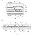
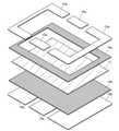
<具体例1>
図7(A)に実施の形態1で例示した発光パネル11の平面図を示し、図7(A)におけ
る一点鎖線A1-A2間の断面図の一例を図7(B)に示す。<Specific example 1>
FIG. 7A shows a plan view of the
図7(B)に示す発光パネルは、素子層101、接着層105、基板103を有する。素
子層101は、基板201、接着層203、絶縁層205、複数のトランジスタ、導電層
157、絶縁層207、絶縁層209、複数の発光素子、絶縁層211、封止層213、
絶縁層261、着色層259、遮光層257、及び絶縁層255を有する。The light emitting panel shown in FIG. 7B has an
It has an insulating
導電層157は、接続体215を介してFPC108と電気的に接続する。The
発光素子230は、下部電極231、EL層233、及び上部電極235を有する。下部
電極231は、トランジスタ240のソース電極又はドレイン電極と電気的に接続する。
下部電極231の端部は、絶縁層211で覆われている。発光素子230はトップエミッ
ション構造である。上部電極235は透光性を有し、EL層233が発する光を透過する
。The
The end of the
発光素子230と重なる位置に、着色層259が設けられ、絶縁層211と重なる位置に
遮光層257が設けられている。着色層259及び遮光層257は絶縁層261で覆われ
ている。発光素子230と絶縁層261の間は封止層213で充填されている。A
発光パネルは、光取り出し部104及び駆動回路部106に、トランジスタ240等の複
数のトランジスタを有する。トランジスタ240は、絶縁層205上に設けられている。
絶縁層205と基板201は接着層203によって貼り合わされている。また、絶縁層2
55と基板103は接着層105によって貼り合わされている。絶縁層205や絶縁層2
55に透水性の低い膜を用いると、発光素子230やトランジスタ240に水等の不純物
が侵入することを抑制でき、発光パネルの信頼性が高くなるため好ましい。接着層203
は、接着層105と同様の材料を用いることができる。The light emitting panel has a plurality of transistors such as
The insulating
The 55 and the
It is preferable to use a film having low water permeability for 55 because impurities such as water can be suppressed from entering the
Can use the same material as the
具体例1では、耐熱性の高い作製基板上で絶縁層205やトランジスタ240、発光素子
230を作製し、該作製基板を剥離し、接着層203を用いて基板201上に絶縁層20
5やトランジスタ240、発光素子230を転置することで作製できる発光パネルを示し
ている。また、具体例1では、耐熱性の高い作製基板上で絶縁層255、着色層259及
び遮光層257を作製し、該作製基板を剥離し、接着層105を用いて基板103上に絶
縁層255、着色層259及び遮光層257を転置することで作製できる発光パネルを示
している。In Specific Example 1, the insulating
A light emitting panel that can be manufactured by transposing 5, a
基板に、耐熱性が低い材料(樹脂など)を用いる場合、作製工程で基板に高温をかけるこ
とが難しいため、該基板上にトランジスタや絶縁膜を作製する条件に制限がある。また、
発光装置の基板に透水性が高い材料(樹脂など)を用いる場合、基板と発光素子の間に、
高温をかけて、透水性の低い膜を形成することが好ましい。本実施の形態の作製方法では
、耐熱性の高い作製基板上でトランジスタ等の作製を行えるため、高温をかけて、信頼性
の高いトランジスタや十分に透水性の低い絶縁膜を形成することができる。そして、それ
らを耐熱性の低い基板へと転置することで、信頼性の高い発光パネルを作製できる。これ
により、本発明の一態様では、軽量又は薄型であり、且つ信頼性の高い発光装置を実現で
きる。作製方法の詳細は後述する。When a material having low heat resistance (resin or the like) is used for the substrate, it is difficult to apply a high temperature to the substrate in the manufacturing process, so that the conditions for forming a transistor or an insulating film on the substrate are limited. again,
When a highly permeable material (resin, etc.) is used for the substrate of the light emitting device, between the substrate and the light emitting element,
It is preferable to apply a high temperature to form a film having low water permeability. In the manufacturing method of this embodiment, a transistor or the like can be manufactured on a manufacturing substrate having high heat resistance, so that a highly reliable transistor or an insulating film having sufficiently low water permeability can be formed by applying a high temperature. .. Then, by transposing them onto a substrate having low heat resistance, a highly reliable light emitting panel can be produced. Thereby, in one aspect of the present invention, it is possible to realize a light emitting device that is lightweight or thin and has high reliability. Details of the manufacturing method will be described later.
基板103及び基板201には、それぞれ、靱性が高い材料を用いることが好ましい。こ
れにより、耐衝撃性に優れ、破損しにくい発光パネルを実現できる。例えば、基板103
を有機樹脂基板とし、基板201を厚さの薄い金属材料や合金材料を用いた基板とするこ
とで、基板にガラス基板を用いる場合に比べて、軽量であり、破損しにくい発光パネルを
実現できる。It is preferable to use a material having high toughness for the
By using an organic resin substrate and a
金属材料や合金材料は熱伝導性が高く、基板全体に熱を容易に伝導できるため、発光パネ
ルの局所的な温度上昇を抑制することができ、好ましい。金属材料や合金材料を用いた基
板の厚さは、10μm以上200μm以下が好ましく、20μm以上50μm以下である
ことがより好ましい。Metallic materials and alloy materials have high thermal conductivity and can easily conduct heat to the entire substrate, so that local temperature rise of the light emitting panel can be suppressed, which is preferable. The thickness of the substrate using the metal material or alloy material is preferably 10 μm or more and 200 μm or less, and more preferably 20 μm or more and 50 μm or less.
また、基板201に、熱放射率が高い材料を用いると発光パネルの表面温度が高くなるこ
とを抑制でき、発光パネルの破壊や信頼性の低下を抑制できる。例えば、基板201を金
属基板と熱放射率の高い層(例えば、金属酸化物やセラミック材料を用いることができる
)の積層構造としてもよい。Further, when a material having a high thermal emissivity is used for the
<具体例2>
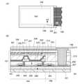
図8(A)に発光パネルにおける光取り出し部104の別の例を示す。図8(A)の発光
パネルは、タッチ操作が可能な発光パネルである。なお、以下の各具体例では、具体例1
と同様の構成については説明を省略する。<Specific example 2>
FIG. 8A shows another example of the
The description of the same configuration as the above will be omitted.
図8(A)に示す発光パネルは、素子層101、接着層105、基板103を有する。素
子層101は、基板201、接着層203、絶縁層205、複数のトランジスタ、絶縁層
207、絶縁層209、複数の発光素子、絶縁層211、絶縁層217、封止層213、
絶縁層261、着色層259、遮光層257、複数の受光素子、導電層281、導電層2
83、絶縁層291、絶縁層293、絶縁層295、及び絶縁層255を有する。The light emitting panel shown in FIG. 8A has an
Insulating
It has 83, an insulating
具体例2では、絶縁層211上に絶縁層217を有する。絶縁層217を設けることで、
基板103と基板201の間隔を調整することができる。In the second embodiment, the insulating
The distance between the
図8(A)では、絶縁層255及び封止層213の間に受光素子を有する例を示す。発光
パネルの非発光領域(例えばトランジスタや配線が設けられた領域など、発光素子が設け
られていない領域)に重ねて受光素子を配置することができるため、画素(発光素子)の
開口率を低下させることなく発光パネルにタッチセンサを設けることができる。FIG. 8A shows an example in which a light receiving element is provided between the insulating
発光パネルが有する受光素子には、例えば、pn型又はpin型のフォトダイオードを用
いることができる。本実施の形態では、受光素子として、p型半導体層271、i型半導
体層273、及びn型半導体層275を有するpin型のフォトダイオードを用いる。For the light receiving element of the light emitting panel, for example, a pn type or pin type photodiode can be used. In the present embodiment, a pin-type photodiode having a p-
なお、i型半導体層273は、含まれるp型を付与する不純物及びn型を付与する不純物
がそれぞれ1×1020cm-3以下の濃度であり、暗伝導度に対して光伝導度が100
倍以上である。i型半導体層273には、周期表第13族もしくは第15族の不純物元素
を有するものもその範疇に含む。すなわち、i型の半導体は、価電子制御を目的とした不
純物元素を意図的に添加しないときに弱いn型の電気伝導性を示すので、i型半導体層2
73は、p型を付与する不純物元素を、成膜時或いは成膜後に、意図的もしくは非意図的
に添加されたものをその範疇に含む。The i-
More than double. The i-
73 includes those in which the impurity element that imparts the p-type is intentionally or unintentionally added at the time of film formation or after film formation.
遮光層257は、受光素子よりも基板201側に位置しており、受光素子と重なる。受光
素子と封止層213との間に位置する遮光層257によって、発光素子230の発する光
が受光素子に照射されることを抑制できる。The light-
導電層281及び導電層283は、それぞれ受光素子と電気的に接続する。導電層281
は、受光素子に入射する光を透過する導電層を用いることが好ましい。導電層283は、
受光素子に入射する光を遮る導電層を用いることが好ましい。The
It is preferable to use a conductive layer that transmits light incident on the light receiving element. The
It is preferable to use a conductive layer that blocks light incident on the light receiving element.
光学式タッチセンサを基板103と封止層213の間に有すると、発光素子230の発光
の影響を受けにくく、S/N比を向上させることができるため、好ましい。It is preferable to have an optical touch sensor between the
<具体例3>
図8(B)に発光パネルにおける光取り出し部104の別の例を示す。図8(B)の発光
パネルは、タッチ操作が可能な発光パネルである。<Specific example 3>
FIG. 8B shows another example of the
図8(B)に示す発光パネルは、素子層101、接着層105、基板103を有する。素
子層101は、基板201、接着層203、絶縁層205、複数のトランジスタ、絶縁層
207、絶縁層209a、絶縁層209b、複数の発光素子、絶縁層211、絶縁層21
7、封止層213、着色層259、遮光層257、複数の受光素子、導電層280、導電
層281、及び絶縁層255を有する。The light emitting panel shown in FIG. 8B has an
7. It has a
図8(B)では、絶縁層205及び封止層213の間に受光素子を有する例を示す。受光
素子を絶縁層205及び封止層213の間に設けることで、トランジスタ240を構成す
る導電層や半導体層と同一の材料、同一の工程で、受光素子と電気的に接続する導電層や
受光素子を構成する光電変換層を作製できる。したがって、作製工程を大きく増加させる
ことなく、タッチ操作が可能な発光パネルを作製できる。FIG. 8B shows an example in which a light receiving element is provided between the insulating
<具体例4>
図9(A)に発光パネルの別の例を示す。図9(A)の発光パネルは、タッチ操作が可能
な発光パネルである。<Specific example 4>
FIG. 9A shows another example of the light emitting panel. The light emitting panel of FIG. 9A is a light emitting panel that can be touch-operated.
図9(A)に示す発光パネルは、素子層101、接着層105、基板103を有する。素
子層101は、基板201、接着層203、絶縁層205、複数のトランジスタ、導電層
156、導電層157、絶縁層207、絶縁層209、複数の発光素子、絶縁層211、
絶縁層217、封止層213、着色層259、遮光層257、絶縁層255、導電層27
2、導電層274、絶縁層276、絶縁層278、導電層294、及び導電層296を有
する。The light emitting panel shown in FIG. 9A has an
Insulating
2. It has a
図9(A)では、絶縁層255及び封止層213の間に静電容量式のタッチセンサを有す
る例を示す。静電容量式のタッチセンサは、導電層272及び導電層274を有する。FIG. 9A shows an example in which a capacitive touch sensor is provided between the insulating
導電層156及び導電層157は、接続体215を介してFPC108と電気的に接続す
る。導電層294及び導電層296は、導電性粒子292を介して導電層274と電気的
に接続する。したがって、FPC108を介して静電容量式のタッチセンサを駆動するこ
とができる。The
<具体例5>
図9(B)に発光パネルの別の例を示す。図9(B)の発光パネルは、タッチ操作が可能
な発光パネルである。<Specific example 5>
FIG. 9B shows another example of the light emitting panel. The light emitting panel of FIG. 9B is a light emitting panel that can be touch-operated.
図9(B)に示す発光パネルは、素子層101、接着層105、基板103を有する。素
子層101は、基板201、接着層203、絶縁層205、複数のトランジスタ、導電層
156、導電層157、絶縁層207、絶縁層209、複数の発光素子、絶縁層211、
絶縁層217、封止層213、着色層259、遮光層257、絶縁層255、導電層27
0、導電層272、導電層274、絶縁層276、及び絶縁層278を有する。The light emitting panel shown in FIG. 9B has an
Insulating
0, has a
図9(B)では、絶縁層255及び封止層213の間に静電容量式のタッチセンサを有す
る例を示す。静電容量式のタッチセンサは、導電層272及び導電層274を有する。FIG. 9B shows an example in which a capacitive touch sensor is provided between the insulating
導電層156及び導電層157は、接続体215aを介してFPC108aと電気的に接
続する。導電層270は、接続体215bを介してFPC108bと電気的に接続する。
したがって、FPC108aを介して発光素子230やトランジスタ240を駆動し、F
PC108bを介して静電容量式のタッチセンサを駆動することができる。The
Therefore, the
A capacitive touch sensor can be driven via the PC108b.
<具体例6>
図10(A)に発光パネルにおける光取り出し部104の別の例を示す。<Specific example 6>
FIG. 10A shows another example of the
図10(A)に示す発光パネルは、素子層101、基板103、接着層105を有する。
素子層101は、基板202、絶縁層205、複数のトランジスタ、絶縁層207、導電
層208、絶縁層209a、絶縁層209b、複数の発光素子、絶縁層211、封止層2
13、及び着色層259を有する。The light emitting panel shown in FIG. 10A has an
The
It has 13 and a
発光素子230は、下部電極231、EL層233、及び上部電極235を有する。下部
電極231は、導電層208を介してトランジスタ240のソース電極又はドレイン電極
と電気的に接続する。下部電極231の端部は、絶縁層211で覆われている。発光素子
230はボトムエミッション構造である。下部電極231は透光性を有し、EL層233
が発する光を透過する。The
Transmits the light emitted by.
発光素子230と重なる位置に、着色層259が設けられ、発光素子230が発する光は
、着色層259を介して基板103側に取り出される。発光素子230と基板202の間
は封止層213で充填されている。基板202は、前述の基板201と同様の材料を用い
て作製できる。A
<具体例7>
図10(B)に発光パネルの別の例を示す。<Specific example 7>
FIG. 10B shows another example of the light emitting panel.
図10(B)に示す発光パネルは、素子層101、接着層105、基板103を有する。
素子層101は、基板202、絶縁層205、導電層310a、導電層310b、複数の
発光素子、絶縁層211、導電層212、及び封止層213を有する。The light emitting panel shown in FIG. 10B has an
The
導電層310a及び導電層310bは、発光パネルの外部接続電極であり、FPC等と電
気的に接続させることができる。The
発光素子230は、下部電極231、EL層233、及び上部電極235を有する。下部
電極231の端部は、絶縁層211で覆われている。発光素子230はボトムエミッショ
ン構造である。下部電極231は透光性を有し、EL層233が発する光を透過する。導
電層212は、下部電極231と電気的に接続する。The
基板103は、光取り出し構造として、半球レンズ、マイクロレンズアレイ、凹凸構造が
施されたフィルム、光拡散フィルム等を有していてもよい。例えば、樹脂基板上に上記レ
ンズやフィルムを、該基板又は該レンズもしくはフィルムと同程度の屈折率を有する接着
剤等を用いて接着することで、光取り出し構造を有する基板103を形成することができ
る。The
導電層212は必ずしも設ける必要は無いが、下部電極231の抵抗に起因する電圧降下
を抑制できるため、設けることが好ましい。また、同様の目的で、上部電極235と電気
的に接続する導電層を絶縁層211上、EL層233上、又は上部電極235上などに設
けてもよい。Although it is not always necessary to provide the
導電層212は、銅、チタン、タンタル、タングステン、モリブデン、クロム、ネオジム
、スカンジウム、ニッケル、アルミニウムから選ばれた材料又はこれらを主成分とする合
金材料等を用いて、単層で又は積層して形成することができる。導電層212の膜厚は、
例えば、0.1μm以上3μm以下とすることができ、好ましくは、0.1μm以上0.
5μm以下である。The
For example, it can be 0.1 μm or more and 3 μm or less, preferably 0.1 μm or more and 0.
It is 5 μm or less.
上部電極235と電気的に接続する導電層の材料にペースト(銀ペーストなど)を用いる
と、該導電層を構成する金属が粒状になって凝集する。そのため、該導電層の表面が粗く
隙間の多い構成となり、例えば、絶縁層211上に該導電層を形成しても、EL層233
が該導電層を完全に覆うことが難しく、上部電極と該導電層との電気的な接続をとること
が容易になり好ましい。When a paste (silver paste or the like) is used as the material of the conductive layer electrically connected to the
However, it is difficult to completely cover the conductive layer, and it is easy to establish an electrical connection between the upper electrode and the conductive layer, which is preferable.
<材料の一例>
次に、発光パネルに用いることができる材料等を説明する。なお、本実施の形態中で先に
説明した構成については説明を省略する。<Example of material>
Next, materials and the like that can be used for the light emitting panel will be described. The configuration described above in the present embodiment will be omitted.
素子層101は、少なくとも発光素子を有する。発光素子としては、自発光が可能な素子
を用いることができ、電流又は電圧によって輝度が制御される素子をその範疇に含んでい
る。例えば、発光ダイオード(LED)、有機EL素子、無機EL素子等を用いることが
できる。The
素子層101は、発光素子を駆動するためのトランジスタや、タッチセンサ等をさらに有
していてもよい。The
発光パネルが有するトランジスタの構造は特に限定されない。例えば、スタガ型のトラン
ジスタとしてもよいし、逆スタガ型のトランジスタとしてもよい。また、トップゲート型
又はボトムゲート型のいずれのトランジスタ構造としてもよい。トランジスタに用いる半
導体材料は特に限定されず、例えば、シリコン、ゲルマニウム等が挙げられる。または、
In-Ga-Zn系金属酸化物などの、インジウム、ガリウム、亜鉛のうち少なくとも一
つを含む酸化物半導体を用いてもよい。The structure of the transistor included in the light emitting panel is not particularly limited. For example, it may be a stagger type transistor or an inverted stagger type transistor. Further, either a top gate type or bottom gate type transistor structure may be used. The semiconductor material used for the transistor is not particularly limited, and examples thereof include silicon and germanium. or,
An oxide semiconductor containing at least one of indium, gallium, and zinc, such as an In—Ga—Zn-based metal oxide, may be used.
トランジスタに用いる半導体材料の結晶性についても特に限定されず、非晶質半導体、結
晶性を有する半導体(微結晶半導体、多結晶半導体、単結晶半導体、又は一部に結晶領域
を有する半導体)のいずれを用いてもよい。結晶性を有する半導体を用いると、トランジ
スタ特性の劣化を抑制できるため好ましい。The crystallinity of the semiconductor material used for the transistor is not particularly limited, and either an amorphous semiconductor or a semiconductor having crystallinity (a fine crystal semiconductor, a polycrystalline semiconductor, a single crystal semiconductor, or a semiconductor having a partially crystallized region). May be used. It is preferable to use a semiconductor having crystallinity because deterioration of transistor characteristics can be suppressed.
発光パネルが有する発光素子は、一対の電極(下部電極231及び上部電極235)と、
該一対の電極間に設けられたEL層233とを有する。該一対の電極の一方は陽極として
機能し、他方は陰極として機能する。The light emitting element of the light emitting panel includes a pair of electrodes (
It has an
発光素子は、トップエミッション構造、ボトムエミッション構造、デュアルエミッション
構造のいずれであってもよい。光を取り出す側の電極には、可視光を透過する導電膜を用
いる。また、光を取り出さない側の電極には、可視光を反射する導電膜を用いることが好
ましい。The light emitting element may have a top emission structure, a bottom emission structure, or a dual emission structure. A conductive film that transmits visible light is used for the electrode on the side that extracts light. Further, it is preferable to use a conductive film that reflects visible light for the electrode on the side that does not take out light.
可視光を透過する導電膜は、例えば、酸化インジウム、インジウム錫酸化物(ITO:I
ndium Tin Oxide)、インジウム亜鉛酸化物、酸化亜鉛、ガリウムを添加
した酸化亜鉛などを用いて形成することができる。また、金、銀、白金、マグネシウム、
ニッケル、タングステン、クロム、モリブデン、鉄、コバルト、銅、パラジウム、もしく
はチタン等の金属材料、これら金属材料を含む合金、又はこれら金属材料の窒化物(例え
ば、窒化チタン)等も、透光性を有する程度に薄く形成することで用いることができる。
また、上記材料の積層膜を導電膜として用いることができる。例えば、銀とマグネシウム
の合金とITOの積層膜などを用いると、導電性を高めることができるため好ましい。ま
た、グラフェン等を用いてもよい。The conductive film that transmits visible light is, for example, indium oxide or indium tin oxide (ITO: I).
It can be formed by using ndium Tin Oxide), indium zinc oxide, zinc oxide, zinc oxide added with gallium, or the like. Also, gold, silver, platinum, magnesium,
Metallic materials such as nickel, tungsten, chromium, molybdenum, iron, cobalt, copper, palladium, or titanium, alloys containing these metal materials, or nitrides of these metal materials (for example, titanium nitride) also have translucency. It can be used by forming it as thin as it has.
Further, the laminated film of the above material can be used as a conductive film. For example, it is preferable to use a laminated film of an alloy of silver and magnesium and ITO because the conductivity can be enhanced. Further, graphene or the like may be used.
可視光を反射する導電膜は、例えば、アルミニウム、金、白金、銀、ニッケル、タングス
テン、クロム、モリブデン、鉄、コバルト、銅、もしくはパラジウム等の金属材料、又は
これら金属材料を含む合金を用いることができる。また、上記金属材料や合金に、ランタ
ン、ネオジム、又はゲルマニウム等が添加されていてもよい。また、アルミニウムとチタ
ンの合金、アルミニウムとニッケルの合金、アルミニウムとネオジムの合金等のアルミニ
ウムを含む合金(アルミニウム合金)や、銀と銅の合金、銀とパラジウムと銅の合金、銀
とマグネシウムの合金等の銀を含む合金を用いて形成することができる。銀と銅を含む合
金は、耐熱性が高いため好ましい。さらに、アルミニウム合金膜に接する金属膜又は金属
酸化物膜を積層することで、アルミニウム合金膜の酸化を抑制することができる。該金属
膜、金属酸化物膜の材料としては、チタン、酸化チタンなどが挙げられる。また、上記可
視光を透過する導電膜と金属材料からなる膜とを積層してもよい。例えば、銀とITOの
積層膜、銀とマグネシウムの合金とITOの積層膜などを用いることができる。As the conductive film that reflects visible light, for example, a metal material such as aluminum, gold, platinum, silver, nickel, tungsten, chromium, molybdenum, iron, cobalt, copper, or palladium, or an alloy containing these metal materials shall be used. Can be done. Further, lanthanum, neodymium, germanium or the like may be added to the above metal materials or alloys. Also, alloys containing aluminum (aluminum alloys) such as alloys of aluminum and titanium, alloys of aluminum and nickel, alloys of aluminum and neodym, alloys of silver and copper, alloys of silver and palladium and copper, alloys of silver and magnesium. It can be formed by using an alloy containing silver such as. Alloys containing silver and copper are preferred because of their high heat resistance. Further, by laminating a metal film or a metal oxide film in contact with the aluminum alloy film, oxidation of the aluminum alloy film can be suppressed. Examples of the material of the metal film and the metal oxide film include titanium and titanium oxide. Further, the conductive film that transmits the visible light and the film made of a metal material may be laminated. For example, a laminated film of silver and ITO, a laminated film of an alloy of silver and magnesium and ITO can be used.
電極は、それぞれ、蒸着法やスパッタリング法を用いて形成すればよい。そのほか、イン
クジェット法などの吐出法、スクリーン印刷法などの印刷法、又はメッキ法を用いて形成
することができる。The electrodes may be formed by using a vapor deposition method or a sputtering method, respectively. In addition, it can be formed by using a ejection method such as an inkjet method, a printing method such as a screen printing method, or a plating method.
下部電極231及び上部電極235の間に、発光素子の閾値電圧より高い電圧を印加する
と、EL層233に陽極側から正孔が注入され、陰極側から電子が注入される。注入され
た電子と正孔はEL層233において再結合し、EL層233に含まれる発光物質が発光
する。When a voltage higher than the threshold voltage of the light emitting element is applied between the
EL層233は少なくとも発光層を有する。EL層233は、発光層以外の層として、正
孔注入性の高い物質、正孔輸送性の高い物質、正孔ブロック材料、電子輸送性の高い物質
、電子注入性の高い物質、又はバイポーラ性の物質(電子輸送性及び正孔輸送性が高い物
質)等を含む層をさらに有していてもよい。The
EL層233には低分子系化合物及び高分子系化合物のいずれを用いることもでき、無機
化合物を含んでいてもよい。EL層233を構成する層は、それぞれ、蒸着法(真空蒸着
法を含む)、転写法、印刷法、インクジェット法、塗布法等の方法で形成することができ
る。Either a low molecular weight compound or a high molecular weight compound can be used for the
素子層101において、発光素子は、一対の透水性の低い絶縁膜の間に設けられているこ
とが好ましい。これにより、発光素子に水等の不純物が侵入することを抑制でき、発光装
置の信頼性の低下を抑制できる。In the
透水性の低い絶縁膜としては、窒化シリコン膜、窒化酸化シリコン膜等の窒素と珪素を含
む膜や、窒化アルミニウム膜等の窒素とアルミニウムを含む膜等が挙げられる。また、酸
化シリコン膜、酸化窒化シリコン膜、酸化アルミニウム膜等を用いてもよい。Examples of the insulating film having low water permeability include a film containing nitrogen and silicon such as a silicon nitride film and a silicon nitride film, and a film containing nitrogen and aluminum such as an aluminum nitride film. Further, a silicon oxide film, a silicon nitride film, an aluminum oxide film and the like may be used.
例えば、透水性の低い絶縁膜の水蒸気透過量は、1×10⁻⁵[g/m2・day]以下
、好ましくは1×10⁻⁶[g/m2・day]以下、より好ましくは1×10-7[g
/m2・day]以下、さらに好ましくは1×10-8[g/m2・day]以下とする
。For example, the water vapor permeation amount of the insulating film having low water permeability is 1 × 10⁻⁵ [g / m2 · day] or less, preferably 1 × 10⁻⁶ [g / m2 · day] or less, more preferably 1. ×10-7 [g
/ M2 · day] or less, more preferably 1 × 10⁻⁸ [g / m2 · day] or less.
基板103は透光性を有し、少なくとも素子層101が有する発光素子の発する光を透過
する。基板103は可撓性を有していてもよい。また、基板103の屈折率は、大気の屈
折率よりも高い。The
ガラスに比べて有機樹脂は重量が軽いため、基板103として有機樹脂を用いると、ガラ
スを用いる場合に比べて発光装置を軽量化でき、好ましい。Since the weight of the organic resin is lighter than that of glass, it is preferable to use the organic resin as the
可撓性及び可視光に対する透過性を有する材料としては、例えば、可撓性を有する程度の
厚さのガラスや、ポリエチレンテレフタレート(PET)、ポリエチレンナフタレート(
PEN)等のポリエステル樹脂、ポリアクリロニトリル樹脂、ポリイミド樹脂、ポリメチ
ルメタクリレート樹脂、ポリカーボネート(PC)樹脂、ポリエーテルスルホン(PES
)樹脂、ポリアミド樹脂、シクロオレフィン樹脂、ポリスチレン樹脂、ポリアミドイミド
樹脂、ポリ塩化ビニル樹脂等が挙げられる。特に、熱膨張係数の低い材料を用いることが
好ましく、例えば、ポリアミドイミド樹脂、ポリイミド樹脂、PET等を好適に用いるこ
とができる。また、ガラス繊維に有機樹脂を含浸した基板や、無機フィラーを有機樹脂に
混ぜて熱膨張係数を下げた基板を使用することもできる。Examples of the material having flexibility and transparency to visible light include glass having a thickness sufficient to have flexibility, polyethylene terephthalate (PET), and polyethylene naphthalate (.
Polyester resin such as PEN), polyacrylonitrile resin, polyimide resin, polymethylmethacrylate resin, polycarbonate (PC) resin, polyether sulfone (PES)
) Resins, polyamide resins, cycloolefin resins, polystyrene resins, polyamideimide resins, polyvinyl chloride resins and the like. In particular, it is preferable to use a material having a low coefficient of thermal expansion, and for example, a polyamide-imide resin, a polyimide resin, PET and the like can be preferably used. Further, a substrate in which glass fiber is impregnated with an organic resin or a substrate in which an inorganic filler is mixed with an organic resin to lower the coefficient of thermal expansion can also be used.
基板103としては、上記材料を用いた層が、発光装置の表面を傷などから保護するハー
ドコート層(例えば、窒化シリコン層など)や、押圧を分散可能な材質の層(例えば、ア
ラミド樹脂層など)等と積層されて構成されていてもよい。また、水分等による発光素子
の寿命の低下等を抑制するために、前述の透水性の低い絶縁膜を有していてもよい。As the
接着層105は、透光性を有し、少なくとも素子層101が有する発光素子の発する光を
透過する。また、接着層105の屈折率は、大気の屈折率よりも高い。The
接着層105には、二液混合型の樹脂などの常温で硬化する樹脂、光硬化性の樹脂、熱硬
化性の樹脂などの樹脂を用いることができる。例えば、エポキシ樹脂、アクリル樹脂、シ
リコーン樹脂、フェノール樹脂等が挙げられる。特に、エポキシ樹脂等の透湿性が低い材
料が好ましい。For the
また、上記樹脂に乾燥剤を含んでいてもよい。例えば、アルカリ土類金属の酸化物(酸化
カルシウムや酸化バリウム等)のように、化学吸着によって水分を吸着する物質を用いる
ことができる。または、ゼオライトやシリカゲル等のように、物理吸着によって水分を吸
着する物質を用いてもよい。乾燥剤が含まれていると、水分などの不純物が発光素子に侵
入することを抑制でき、発光装置の信頼性が向上するため好ましい。Further, the resin may contain a desiccant. For example, a substance that adsorbs water by chemisorption, such as an oxide of an alkaline earth metal (calcium oxide, barium oxide, etc.), can be used. Alternatively, a substance that adsorbs water by physical adsorption, such as zeolite or silica gel, may be used. When a desiccant is contained, impurities such as moisture can be suppressed from entering the light emitting element, and the reliability of the light emitting device is improved, which is preferable.
また、上記樹脂に屈折率の高いフィラー(酸化チタン等)を混合することにより、発光素
子からの光取り出し効率を向上させることができ、好ましい。Further, by mixing the resin with a filler having a high refractive index (titanium oxide or the like), the efficiency of light extraction from the light emitting element can be improved, which is preferable.
また、接着層105には、光を散乱させる散乱部材を有していてもよい。例えば、接着層
105には、上記樹脂と上記樹脂と屈折率が異なる粒子との混合物を用いることもできる
。該粒子は光の散乱部材として機能する。Further, the
樹脂と、該樹脂と屈折率の異なる粒子は、屈折率の差が0.1以上あることが好ましく、
0.3以上あることがより好ましい。具体的には樹脂としては、エポキシ樹脂、アクリル
樹脂、イミド樹脂、シリコーン等を用いることができる。また粒子としては、酸化チタン
、酸化バリウム、ゼオライト等を用いることができる。It is preferable that the resin and the particles having a different refractive index from the resin have a difference in refractive index of 0.1 or more.
More preferably, it is 0.3 or more. Specifically, as the resin, epoxy resin, acrylic resin, imide resin, silicone and the like can be used. Further, as the particles, titanium oxide, barium oxide, zeolite or the like can be used.
酸化チタンおよび酸化バリウムの粒子は、光を散乱させる性質が強く好ましい。またゼオ
ライトを用いると、樹脂等の有する水を吸着することができ、発光素子の信頼性を向上さ
せることができる。Titanium oxide and barium oxide particles have a strong and preferable property of scattering light. Further, when zeolite is used, water contained in a resin or the like can be adsorbed, and the reliability of the light emitting element can be improved.
絶縁層205、絶縁層255には、無機絶縁材料を用いることができる。特に、前述の透
水性の低い絶縁膜を用いると、信頼性の高い発光パネルを実現できるため好ましい。Inorganic insulating materials can be used for the insulating
絶縁層207は、トランジスタを構成する半導体への不純物の拡散を抑制する効果を奏す
る。絶縁層207としては、酸化シリコン膜、酸化窒化シリコン膜、窒化シリコン膜、窒
化酸化シリコン膜、酸化アルミニウム膜などの無機絶縁膜を用いることができる。The insulating
絶縁層209、絶縁層209a、及び絶縁層209bとしては、それぞれ、トランジスタ
起因等の表面凹凸を低減するために平坦化機能を有する絶縁膜を選択するのが好適である
。例えば、ポリイミド、アクリル、ベンゾシクロブテン系樹脂等の有機材料を用いること
ができる。また、上記有機材料の他に、低誘電率材料(low-k材料)等を用いること
ができる。なお、これらの材料で形成される絶縁膜や無機絶縁膜を用いた積層構造として
もよい。As the insulating
絶縁層211は、下部電極231の端部を覆って設けられている。絶縁層211の上層に
形成されるEL層233や上部電極235の被覆性を良好なものとするため、絶縁層21
1の側壁が連続した曲率を持って形成される傾斜面となることが好ましい。The insulating
It is preferable that the side wall of 1 is an inclined surface formed with a continuous curvature.
絶縁層211の材料としては、樹脂又は無機絶縁材料を用いることができる。樹脂として
は、例えば、ポリイミド樹脂、ポリアミド樹脂、アクリル樹脂、シロキサン樹脂、エポキ
シ樹脂、又はフェノール樹脂等を用いることができる。特に、絶縁層211の作製が容易
となるため、ネガ型の感光性樹脂、あるいはポジ型の感光性樹脂を用いることが好ましい
。As the material of the insulating
絶縁層211の形成方法は、特に限定されないが、フォトリソグラフィ法、スパッタ法、
蒸着法、液滴吐出法(インクジェット法等)、印刷法(スクリーン印刷、オフセット印刷
等)等を用いればよい。The method for forming the insulating
A vapor deposition method, a droplet ejection method (inkjet method, etc.), a printing method (screen printing, offset printing, etc.) or the like may be used.
絶縁層217は、無機絶縁材料又は有機絶縁材料等を用いて形成することができる。例え
ば、有機絶縁材料としては、ネガ型やポジ型の感光性樹脂、非感光性樹脂などを用いるこ
とができる。また、絶縁層217にかえて、導電層を形成してもよい。例えば、金属材料
を用いて形成することができる。金属材料としては、チタン、アルミニウムなどを用いる
ことができる。絶縁層217の代わりに導電層を用い、該導電層と上部電極235とを電
気的に接続させる構成とすることで、上部電極235の抵抗に起因した電位降下を抑制で
きる。また、絶縁層217は、順テーパ形状であっても逆テーパ形状であってもよい。The insulating
絶縁層276、絶縁層278、絶縁層291、絶縁層293、絶縁層295は、それぞれ
、無機絶縁材料又は有機絶縁材料を用いて形成できる。特に絶縁層278や絶縁層295
は、センサ素子起因の表面凹凸を低減するために平坦化機能を有する絶縁層を用いること
が好ましい。The insulating
It is preferable to use an insulating layer having a flattening function in order to reduce surface irregularities caused by the sensor element.
封止層213には、二液混合型の樹脂などの常温で硬化する樹脂、光硬化性の樹脂、熱硬
化性の樹脂などの樹脂を用いることができる。例えば、PVC(ポリビニルクロライド)
樹脂、アクリル樹脂、ポリイミド樹脂、エポキシ樹脂、シリコーン樹脂、PVB(ポリビ
ニルブチラル)樹脂、EVA(エチレンビニルアセテート)樹脂等を用いることができる
。封止層213に乾燥剤が含まれていてもよい。また、封止層213を通過して発光素子
230の光が発光パネルの外に取り出される場合は、封止層213に屈折率の高いフィラ
ーや散乱部材を含むことが好ましい。乾燥剤、屈折率の高いフィラー、散乱部材について
は、接着層105に用いることができる材料と同様の材料が挙げられる。For the
Resins, acrylic resins, polyimide resins, epoxy resins, silicone resins, PVB (polyvinyl butyral) resins, EVA (ethylene vinyl acetate) resins and the like can be used. The
導電層156、導電層157、導電層294、及び導電層296は、それぞれ、トランジ
スタ又は発光素子を構成する導電層と同一の材料、同一の工程で形成できる。また、導電
層280は、トランジスタを構成する導電層と同一の材料、同一の工程で形成できる。The
例えば、上記導電層は、それぞれ、モリブデン、チタン、クロム、タンタル、タングステ
ン、アルミニウム、銅、ネオジム、スカンジウム等の金属材料又はこれらの元素を含む合
金材料を用いて、単層で又は積層して形成することができる。また、上記導電層は、それ
ぞれ、導電性の金属酸化物を用いて形成しても良い。導電性の金属酸化物としては酸化イ
ンジウム(In2O3等)、酸化スズ(SnO2等)、酸化亜鉛(ZnO)、ITO、イ
ンジウム亜鉛酸化物(In2O3-ZnO等)又はこれらの金属酸化物材料に酸化シリコ
ンを含ませたものを用いることができる。For example, the conductive layer is formed as a single layer or laminated using a metal material such as molybdenum, titanium, chromium, tantalum, tungsten, aluminum, copper, neodymium, scandium, or an alloy material containing these elements, respectively. can do. Further, each of the conductive layers may be formed by using a conductive metal oxide. Conductive metal oxides include indium oxide (In2 O3 , etc.), tin oxide (SnO2 , etc.), zinc oxide (ZnO), ITO, indium zinc oxide (In2 O3 -ZnO, etc.) or these. A metal oxide material containing silicon oxide can be used.
また、導電層208、導電層212、導電層310a及び導電層310bも、それぞれ、
上記金属材料、合金材料、又は導電性の金属酸化物等を用いて形成できる。Further, the
It can be formed by using the above metal material, alloy material, conductive metal oxide, or the like.
導電層272及び導電層274、並びに、導電層281及び導電層283は、透光性を有
する導電層である。例えば、酸化インジウム、ITO、インジウム亜鉛酸化物、酸化亜鉛
、ガリウムを添加した酸化亜鉛等を用いることができる。また、導電層270は導電層2
72と同一の材料、同一の工程で形成できる。The
It can be formed by the same material and the same process as 72.
導電性粒子292は、有機樹脂またはシリカなどの粒子の表面を金属材料で被覆したもの
を用いる。金属材料としてニッケルや金を用いると接触抵抗を低減できるため好ましい。
またニッケルをさらに金で被覆するなど、2種類以上の金属材料を層状に被覆させた粒子
を用いることが好ましい。As the
Further, it is preferable to use particles in which two or more kinds of metal materials are coated in a layered manner, such as by further coating nickel with gold.
接続体215としては、熱硬化性の樹脂に金属粒子を混ぜ合わせたペースト状又はシート
状の、熱圧着によって異方性の導電性を示す材料を用いることができる。金属粒子として
は、例えばニッケル粒子を金で被覆したものなど、2種類以上の金属が層状となった粒子
を用いることが好ましい。As the connecting
着色層259は特定の波長帯域の光を透過する有色層である。例えば、赤色の波長帯域の
光を透過する赤色(R)のカラーフィルタ、緑色の波長帯域の光を透過する緑色(G)の
カラーフィルタ、青色の波長帯域の光を透過する青色(B)のカラーフィルタなどを用い
ることができる。各着色層は、様々な材料を用いて、印刷法、インクジェット法、フォト
リソグラフィ法を用いたエッチング方法などでそれぞれ所望の位置に形成する。The
また、隣接する着色層259の間に、遮光層257が設けられている。遮光層257は隣
接する発光素子から回り込む光を遮光し、隣接画素間における混色を抑制する。ここで、
着色層259の端部を、遮光層257と重なるように設けることにより、光漏れを抑制す
ることができる。遮光層257は、発光素子の発光を遮光する材料を用いることができ、
金属材料や顔料や染料を含む樹脂材料などを用いて形成することができる。なお、図7(
B)に示すように、遮光層257を駆動回路部106などの光取り出し部104以外の領
域に設けると、導波光などによる意図しない光漏れを抑制できるため好ましい。Further, a light-
By providing the end portion of the
It can be formed by using a metal material, a resin material containing a pigment or a dye, or the like. In addition, FIG. 7 (
As shown in B), it is preferable to provide the light-
また、着色層259と遮光層257を覆う絶縁層261を設けると、着色層259や遮光
層257に含まれる顔料などの不純物が発光素子等に拡散することを抑制できるため好ま
しい。絶縁層261は透光性の材料を用い、無機絶縁材料や有機絶縁材料を用いることが
できる。絶縁層261に前述の透水性の低い絶縁膜を用いてもよい。なお、絶縁層261
は不要であれば設けなくてもよい。Further, it is preferable to provide the insulating
Is not required if it is unnecessary.
<作製方法例>
次に、発光パネルの作製方法を図11及び図12を用いて例示する。ここでは、具体例1
(図7(B))の構成の発光パネルを例に挙げて説明する。<Example of manufacturing method>
Next, a method for manufacturing the light emitting panel will be illustrated with reference to FIGS. 11 and 12. Here, specific example 1
A light emitting panel having the configuration shown in FIG. 7B will be described as an example.
まず、作製基板301上に剥離層303を形成し、剥離層303上に絶縁層205を形成
する。次に、絶縁層205上に複数のトランジスタ、導電層157、絶縁層207、絶縁
層209、複数の発光素子、及び絶縁層211を形成する。なお、導電層157が露出す
るように、絶縁層211、絶縁層209、及び絶縁層207は開口する(図11(A))
。First, the
..
また、作製基板305上に剥離層307を形成し、剥離層307上に絶縁層255を形成
する。次に、絶縁層255上に遮光層257、着色層259、及び絶縁層261を形成す
る(図11(B))。Further, the
作製基板301及び作製基板305としては、それぞれ、ガラス基板、石英基板、サファ
イア基板、セラミック基板、金属基板などを用いることができる。As the
また、ガラス基板には、例えば、アルミノシリケートガラス、アルミノホウケイ酸ガラス
、バリウムホウケイ酸ガラス等のガラス材料を用いることができる。後の加熱処理の温度
が高い場合には、歪み点が730℃以上のものを用いるとよい。なお、酸化バリウム(B
aO)を多く含ませることで、より実用的な耐熱ガラスが得られる。他にも、結晶化ガラ
スなどを用いることができる。Further, as the glass substrate, for example, a glass material such as aluminosilicate glass, aluminoborosilicate glass, and barium borosilicate glass can be used. When the temperature of the subsequent heat treatment is high, it is preferable to use one having a strain point of 730 ° C. or higher. Barium oxide (B)
By containing a large amount of aO), more practical heat-resistant glass can be obtained. In addition, crystallized glass or the like can be used.
作製基板にガラス基板を用いる場合、作製基板と剥離層との間に、酸化シリコン膜、酸化
窒化シリコン膜、窒化シリコン膜、窒化酸化シリコン膜等の絶縁膜を形成すると、ガラス
基板からの汚染を防止でき、好ましい。When a glass substrate is used as the manufacturing substrate, if an insulating film such as a silicon oxide film, a silicon nitride film, a silicon nitride film, or a silicon nitride film is formed between the manufacturing substrate and the release layer, the glass substrate is contaminated. It can be prevented and is preferable.
剥離層303及び剥離層307としては、それぞれ、タングステン、モリブデン、チタン
、タンタル、ニオブ、ニッケル、コバルト、ジルコニウム、亜鉛、ルテニウム、ロジウム
、パラジウム、オスミウム、イリジウム、シリコンから選択された元素、該元素を含む合
金材料、又は該元素を含む化合物材料からなり、単層又は積層された層である。シリコン
を含む層の結晶構造は、非晶質、微結晶、多結晶のいずれでもよい。The
剥離層は、スパッタリング法、プラズマCVD法、塗布法、印刷法等により形成できる。
なお、塗布法は、スピンコーティング法、液滴吐出法、ディスペンス法を含む。The release layer can be formed by a sputtering method, a plasma CVD method, a coating method, a printing method, or the like.
The coating method includes a spin coating method, a droplet ejection method, and a dispensing method.
剥離層が単層構造の場合、タングステン層、モリブデン層、又はタングステンとモリブデ
ンの混合物を含む層を形成することが好ましい。また、タングステンの酸化物もしくは酸
化窒化物を含む層、モリブデンの酸化物もしくは酸化窒化物を含む層、又はタングステン
とモリブデンの混合物の酸化物もしくは酸化窒化物を含む層を形成してもよい。なお、タ
ングステンとモリブデンの混合物とは、例えば、タングステンとモリブデンの合金に相当
する。When the release layer has a single layer structure, it is preferable to form a tungsten layer, a molybdenum layer, or a layer containing a mixture of tungsten and molybdenum. Further, a layer containing a tungsten oxide or an oxide nitride, a layer containing a molybdenum oxide or an oxide nitride, or a layer containing an oxide or an oxide of a mixture of tungsten and molybdenum may be formed. The mixture of tungsten and molybdenum corresponds to, for example, an alloy of tungsten and molybdenum.
また、剥離層として、タングステンを含む層とタングステンの酸化物を含む層の積層構造
を形成する場合、タングステンを含む層を形成し、その上層に酸化物で形成される絶縁膜
を形成することで、タングステン層と絶縁膜との界面に、タングステンの酸化物を含む層
が形成されることを活用してもよい。また、タングステンを含む層の表面を、熱酸化処理
、酸素プラズマ処理、亜酸化窒素(N2O)プラズマ処理、オゾン水等の酸化力の強い溶
液での処理等を行ってタングステンの酸化物を含む層を形成してもよい。またプラズマ処
理や加熱処理は、酸素、窒素、亜酸化窒素単独、あるいは該ガスとその他のガスとの混合
気体雰囲気下で行ってもよい。上記プラズマ処理や加熱処理により、剥離層の表面状態を
変えることにより、剥離層と後に形成される絶縁層との密着性を制御することが可能であ
る。Further, when forming a laminated structure of a layer containing tungsten and a layer containing an oxide of tungsten as a release layer, a layer containing tungsten is formed, and an insulating film formed of an oxide is formed on the layer above the layer. It may be utilized that a layer containing a tungsten oxide is formed at the interface between the tungsten layer and the insulating film. Further, the surface of the layer containing tungsten is subjected to thermal oxidation treatment, oxygen plasma treatment, nitrous oxide( N2O) plasma treatment, treatment with a solution having strong oxidizing power such as ozone water, etc. to obtain the oxide of tungsten. The containing layer may be formed. Further, the plasma treatment and the heat treatment may be performed by oxygen, nitrogen, nitrous oxide alone, or in a mixed gas atmosphere of the gas and another gas. By changing the surface state of the peeling layer by the plasma treatment or the heat treatment, it is possible to control the adhesion between the peeling layer and the insulating layer formed later.
各絶縁層は、スパッタリング法、プラズマCVD法、塗布法、印刷法等を用いて形成する
ことが可能であり、例えば、プラズマCVD法によって成膜温度を250℃以上400℃
以下として形成することで、緻密で非常に透水性の低い膜とすることができる。Each insulating layer can be formed by a sputtering method, a plasma CVD method, a coating method, a printing method, or the like. For example, the film formation temperature is 250 ° C. or higher and 400 ° C. by the plasma CVD method.
By forming as follows, a dense and extremely low water permeability film can be obtained.
その後、作製基板305の着色層259等が設けられた面又は作製基板301の発光素子
230等が設けられた面に封止層213となる材料を塗布し、封止層213を介して該面
同士が対向するように、作製基板301及び作製基板305を貼り合わせる(図11(C
))。After that, a material to be the
)).
そして、作製基板301を剥離し、露出した絶縁層205と基板201を、接着層203
を用いて貼り合わせる。また、作製基板305を剥離し、露出した絶縁層255と基板1
03を、接着層105を用いて貼り合わせる。図12(A)では、基板103が導電層1
57と重ならない構成としたが、導電層157と基板103が重なっていてもよい。Then, the manufactured
Paste together using. Further, the
03 is bonded together using the
Although the configuration does not overlap with 57, the
なお、剥離工程は、様々な方法を適宜用いることができる。例えば、剥離層として、被剥
離層と接する側に金属酸化膜を含む層を形成した場合は、当該金属酸化膜を結晶化により
脆弱化して、被剥離層を作製基板から剥離することができる。また、耐熱性の高い作製基
板と被剥離層の間に、剥離層として水素を含む非晶質珪素膜を形成した場合はレーザ光の
照射又はエッチングにより当該非晶質珪素膜を除去することで、被剥離層を作製基板から
剥離することができる。また、剥離層として、被剥離層と接する側に金属酸化膜を含む層
を形成し、当該金属酸化膜を結晶化により脆弱化し、さらに剥離層の一部を溶液やNF3
、BrF3、ClF3等のフッ化ガスを用いたエッチングで除去した後、脆弱化された金
属酸化膜において剥離することができる。さらには、剥離層として窒素、酸素や水素等を
含む膜(例えば、水素を含む非晶質珪素膜、水素含有合金膜、酸素含有合金膜など)を用
い、剥離層にレーザ光を照射して剥離層内に含有する窒素、酸素や水素をガスとして放出
させ被剥離層と基板との剥離を促進する方法を用いてもよい。また、被剥離層が形成され
た作製基板を機械的に除去又は溶液やNF3、BrF3、ClF3等のフッ化ガスによる
エッチングで除去する方法等を用いることができる。この場合、剥離層を設けなくともよ
い。In addition, various methods can be appropriately used for the peeling step. For example, when a layer containing a metal oxide film is formed on the side in contact with the layer to be peeled as the peeling layer, the metal oxide film can be fragile by crystallization and the layer to be peeled can be peeled from the manufactured substrate. When an amorphous silicon film containing hydrogen is formed as a peeling layer between the highly heat-resistant manufacturing substrate and the layer to be peeled off, the amorphous silicon film is removed by irradiation with laser light or etching. , The layer to be peeled off can be peeled off from the manufactured substrate. Further, as the peeling layer, a layer containing a metal oxide film is formed on the side in contact with the peeled layer, the metal oxide film is weakened by crystallization, and a part of the peeling layer is partially used as a solution or NF3 .
, BrF3 , ClF3 , etc. After removal by etching with a fluorogas, it can be peeled off in a fragile metal oxide film. Furthermore, a film containing nitrogen, oxygen, hydrogen, etc. (for example, an amorphous silicon film containing hydrogen, a hydrogen-containing alloy film, an oxygen-containing alloy film, etc.) is used as the release layer, and the release layer is irradiated with laser light. A method may be used in which nitrogen, oxygen or hydrogen contained in the peeling layer is released as a gas to promote the peeling between the peeled layer and the substrate. Further, a method of mechanically removing the manufactured substrate on which the layer to be peeled is formed or etching with a solution or a fluoride gas such as NF3 , BrF3 , ClF3 or the like can be used. In this case, it is not necessary to provide the release layer.
また、上記剥離方法を複数組み合わせることでより容易に剥離工程を行うことができる。
つまり、レーザ光の照射、ガスや溶液などによる剥離層へのエッチング、鋭いナイフやメ
スなどによる機械的な除去を行い、剥離層と被剥離層とを剥離しやすい状態にしてから、
物理的な力(機械等による)によって剥離を行うこともできる。Further, the peeling step can be performed more easily by combining a plurality of the peeling methods.
In other words, after irradiating the peeling layer with laser light, etching the peeling layer with a gas or solution, and mechanically removing it with a sharp knife or scalpel, the peeling layer and the peeled layer can be easily peeled off.
Peeling can also be performed by physical force (by a machine or the like).
また、剥離層と被剥離層との界面に液体を浸透させて作製基板から被剥離層を剥離しても
よい。また、剥離を行う際に水などの液体をかけながら剥離してもよい。Further, the liquid to be peeled off may be peeled off from the manufactured substrate by infiltrating the liquid into the interface between the peeled layer and the layer to be peeled off. Further, when the peeling is performed, the peeling may be performed while sprinkling a liquid such as water.
その他の剥離方法としては、剥離層をタングステンで形成した場合は、アンモニア水と過
酸化水素水の混合溶液により剥離層をエッチングしながら剥離を行うとよい。As another peeling method, when the peeling layer is formed of tungsten, it is preferable to perform peeling while etching the peeling layer with a mixed solution of aqueous ammonia and hydrogen peroxide.
なお、作製基板と被剥離層の界面で剥離が可能な場合には、剥離層を設けなくてもよい。
例えば、作製基板としてガラスを用い、ガラスに接してポリイミド、ポリエステル、ポリ
オレフィン、ポリアミド、ポリカーボネート、アクリル等の有機樹脂を形成し、有機樹脂
上に絶縁膜やトランジスタ等を形成する。この場合、有機樹脂を加熱することにより、作
製基板と有機樹脂の界面で剥離することができる。又は、作製基板と有機樹脂の間に金属
層を設け、該金属層に電流を流すことで該金属層を加熱し、金属層と有機樹脂の界面で剥
離を行ってもよい。作製基板から剥離した有機樹脂を発光パネルの基板として用いること
ができる。また、有機樹脂と他の基板を接着剤により貼り合わせてもよい。If peeling is possible at the interface between the manufactured substrate and the layer to be peeled off, the peeling layer may not be provided.
For example, glass is used as a manufacturing substrate, and an organic resin such as polyimide, polyester, polyolefin, polyamide, polycarbonate, or acrylic is formed in contact with the glass, and an insulating film, a transistor, or the like is formed on the organic resin. In this case, by heating the organic resin, it can be peeled off at the interface between the production substrate and the organic resin. Alternatively, a metal layer may be provided between the production substrate and the organic resin, the metal layer may be heated by passing an electric current through the metal layer, and peeling may be performed at the interface between the metal layer and the organic resin. The organic resin peeled off from the manufactured substrate can be used as the substrate of the light emitting panel. Further, the organic resin and another substrate may be bonded together with an adhesive.
最後に、絶縁層255及び封止層213を開口することで、導電層157を露出させる(
図12(B))。なお、基板103が導電層157と重なる構成の場合は、導電層157
を露出させるために、基板103及び接着層105も開口する(図12(C))。開口の
手段は特に限定されず、例えばレーザアブレーション法、エッチング法、イオンビームス
パッタリング法などを用いればよい。また、導電層157上の膜に鋭利な刃物等を用いて
切り込みを入れ、物理的な力で膜の一部を引き剥がしてもよい。Finally, the
FIG. 12 (B). When the
The
以上により、発光パネルを作製することができる。From the above, the light emitting panel can be manufactured.
以上に示したように、本実施の形態の発光パネルは、基板103と、基板201又は基板
202と、の2枚の基板で構成される。さらにタッチセンサを含む構成であっても、2枚
の基板で構成することができる。基板の数を最低限とすることで、光の取り出し効率の向
上や表示の鮮明さの向上が容易となる。As shown above, the light emitting panel of the present embodiment is composed of two substrates, a
本実施の形態は、他の実施の形態と適宜組み合わせることができる。This embodiment can be appropriately combined with other embodiments.
(実施の形態3)
本実施の形態では、発光パネルについて図13を用いて説明する。(Embodiment 3)
In this embodiment, the light emitting panel will be described with reference to FIG.
図13に示す発光パネルは、基板401、トランジスタ240、発光素子230、絶縁層
207、絶縁層209、絶縁層211、絶縁層217、空間405、絶縁層261、遮光
層257、着色層259、受光素子(p型半導体層271、i型半導体層273、及びn
型半導体層275を有する)、導電層281、導電層283、絶縁層291、絶縁層29
3、絶縁層295、及び基板403を有する。The light emitting panel shown in FIG. 13 includes a
(Has a type semiconductor layer 275),
3. It has an insulating
該発光パネルは、基板401及び基板403の間に、発光素子230及び受光素子を囲む
ように枠状に配置された接着層(図示しない)を有する。該接着層、基板401及び基板
403によって、発光素子230は封止されている。The light emitting panel has an adhesive layer (not shown) arranged in a frame shape so as to surround the
本実施の形態の発光パネルでは、基板403が透光性を有する。発光素子230の発する
光は、着色層259、基板403等を介して、大気に取り出される。In the light emitting panel of the present embodiment, the
本実施の形態の発光パネルは、タッチ操作が可能な発光パネルである。具体的には、受光
素子を用いて、基板403の表面への被検出物の近接又は接触を検知できる。The light emitting panel of the present embodiment is a light emitting panel that can be touch-operated. Specifically, the light receiving element can be used to detect the proximity or contact of the object to be detected with the surface of the
光学式タッチセンサは、被検出物が接触する表面に傷等がついても検出精度に影響が無い
ため、耐久性が高く好ましい。また、光学式タッチセンサは、非接触によるセンシングが
可能である、表示装置に適用しても画像の鮮明さが低下しない、大型の発光パネルや表示
装置への適用が可能である等の利点もある。The optical touch sensor is preferable because it has high durability because it does not affect the detection accuracy even if the surface to which the object to be detected comes into contact is scratched. In addition, the optical touch sensor has the advantages that it can be sensed by non-contact, the sharpness of the image does not deteriorate even if it is applied to a display device, and it can be applied to a large light emitting panel or a display device. be.
光学式タッチセンサを基板403と空間405の間に有すると、発光素子230の発光の
影響を受けにくく、S/N比を向上させることができるため、好ましい。It is preferable to have the optical touch sensor between the
遮光層257は、受光素子よりも基板401側に位置しており、受光素子と重なる。遮光
層257によって、発光素子230の発する光が受光素子に照射されることを抑制できる
。The light-
基板401及び基板403に用いる材料に特に限定はない。発光素子からの光を取り出す
側の基板には該光を透過する材料を用いる。例えば、ガラス、石英、セラミック、サファ
イア、有機樹脂などの材料を用いることができる。発光を取り出さない側の基板は、透光
性を有していなくてもよいため、上記に挙げた基板の他に、金属材料や合金材料を用いた
金属基板等を用いることもできる。また、基板401及び基板403には、先の実施の形
態で例示した基板の材料も用いることができる。The materials used for the
発光パネルの封止方法は限定されず、例えば、固体封止であっても中空封止であってもよ
い。例えば、封止材として、ガラスフリットなどのガラス材料や、二液混合型の樹脂など
の常温で硬化する樹脂、光硬化性の樹脂、熱硬化性の樹脂などの樹脂を用いることができ
る。空間405は、窒素やアルゴンなどの不活性な気体で充填されていてもよく、封止層
213と同様の樹脂等で充填されていてもよい。また、樹脂内に前述の乾燥剤、屈折率の
高いフィラー、又は散乱部材が含まれていてもよい。The sealing method of the light emitting panel is not limited, and may be, for example, solid sealing or hollow sealing. For example, as the sealing material, a glass material such as a glass frit, a resin that cures at room temperature such as a two-component mixed type resin, a photocurable resin, and a resin such as a thermosetting resin can be used. The
本実施の形態は、他の実施の形態と適宜組み合わせることができる。This embodiment can be appropriately combined with other embodiments.
本実施例では、本発明の一態様の発光装置を作製した。本実施例の発光装置は、3つに折
りたたむことができる屏風タイプ(tri-fold Folding Screen
Type)のディスプレイであるともいえる。In this example, the light emitting device of one aspect of the present invention was produced. The light emitting device of this embodiment is a folding screen type (tri-fold Molding Screen) that can be folded in three.
It can be said that it is a Type) display.
本実施例で作製した発光装置が有する発光パネルを図18(A)、(B)に示す。本実施
例で作製した発光装置は、基板103と基板201の大きさが異なる点と、異なる色の画
素間に絶縁層217を有する点で、実施の形態2で説明した具体例1(図7(B))と異
なる。その他は具体例1などの説明を参照できる。絶縁層217は、具体例2などの説明
を参照できる。The light emitting panels included in the light emitting device manufactured in this embodiment are shown in FIGS. 18A and 18B. The light emitting device produced in this embodiment has a difference in size between the
発光パネルは、実施の形態2に示した作製方法を用いて作製した。The light emitting panel was manufactured by using the manufacturing method shown in the second embodiment.
まず、作製基板301であるガラス基板上に剥離層303を形成し、剥離層303上に被
剥離層を形成した。また、作製基板305であるガラス基板上に剥離層307を形成し、
剥離層307上に被剥離層を形成した。次に、作製基板301と作製基板305とを、そ
れぞれの被剥離層が形成された面が対向するように貼り合わせた。そして、2つの作製基
板をそれぞれ被剥離層から剥離し、それぞれの被剥離層に可撓性基板を貼り合わせた。以
下に各層の材料を示す。First, the
A peeled layer was formed on the peeled
剥離層303及び剥離層307としては、タングステン膜と、該タングステン膜上の酸化
タングステン膜の積層構造を形成した。As the
剥離層を構成する積層構造は、成膜直後の剥離性は低いが、加熱処理により無機絶縁膜と
の反応が起こることで、剥離層と無機絶縁膜の界面の状態が変化し脆性を示す。そして、
剥離の起点を形成することで、物理的に剥離することができるようになる。The laminated structure constituting the release layer has low peelability immediately after film formation, but the state of the interface between the release layer and the inorganic insulating film changes due to the reaction with the inorganic insulating film due to the heat treatment, and exhibits brittleness. and,
By forming the starting point of peeling, it becomes possible to physically peel off.
剥離層303上の被剥離層としては、絶縁層205と、トランジスタと、発光素子230
である有機EL素子と、を形成した。剥離層307上の被剥離層としては、絶縁層255
やカラーフィルタ(着色層259に相当)等を作製した。The layers to be peeled off on the
The organic EL element, which is The layer to be peeled on the
And a color filter (corresponding to the colored layer 259) and the like were produced.
絶縁層205及び絶縁層255としては、それぞれ、酸化窒化シリコン膜及び窒化シリコ
ン膜等を含む積層構造を用いた。As the insulating
トランジスタには、CAAC-OS(C Axis Aligned Crystall
ine Oxide Semiconductor)を用いたトランジスタを適用した。
CAAC-OSは非晶質ではないため、欠陥準位が少なく、トランジスタの信頼性を高め
ることができる。また、CAAC-OSは結晶粒界を有さないため、可撓性を有する装置
を湾曲させたときの応力によってCAAC-OS膜にクラックが生じにくい。The transistor is CAAC-OS (C Axis Aligned Crystal).
A transistor using an ine Oxide Semiconductor) was applied.
Since CAAC-OS is not amorphous, it has few defect levels and can improve the reliability of the transistor. Further, since CAAC-OS does not have grain boundaries, cracks are unlikely to occur in the CAAC-OS film due to stress when the flexible device is bent.
CAAC-OSは、膜面に概略垂直にc軸配向した酸化物半導体のことである。酸化物半
導体の結晶構造としては他にナノスケールの微結晶集合体であるnano-crysta
l(nc)など、アモルファスや単結晶とは異なる多彩な構造が存在することが確認され
ている。CAACは、単結晶よりも結晶性が低いが、アモルファスやncに比べて結晶性
が高い。CAAC-OS is an oxide semiconductor oriented substantially perpendicular to the film surface on the c-axis. Another crystal structure of oxide semiconductors is nano-crysta, which is a nanoscale crystallite aggregate.
It has been confirmed that various structures such as l (nc), which are different from amorphous and single crystals, exist. CAAC has lower crystallinity than single crystal, but higher crystallinity than amorphous and nc.
本実施例では、In-Ga-Zn系酸化物を用いたチャネルエッチ型のトランジスタを用
いた。該トランジスタは、ガラス基板上で500℃未満のプロセスで作製可能である。In this embodiment, a channel-etched transistor using an In—Ga—Zn-based oxide was used. The transistor can be made on a glass substrate by a process of less than 500 ° C.
プラスチック基板等の有機樹脂上に直接トランジスタ等の素子を作製する方法では、素子
の作製工程の温度を、有機樹脂の耐熱温度よりも低くしなくてはならない。本実施例では
、作製基板がガラス基板であり、また、無機膜である剥離層の耐熱性が高いため、ガラス
基板上にトランジスタを作製する場合と同じ温度でトランジスタを作製することができる
ため、トランジスタの性能、信頼性を容易に確保できる。In the method of manufacturing an element such as a transistor directly on an organic resin such as a plastic substrate, the temperature of the device manufacturing process must be lower than the heat resistant temperature of the organic resin. In this embodiment, since the manufacturing substrate is a glass substrate and the heat resistance of the release layer which is an inorganic film is high, the transistor can be manufactured at the same temperature as when the transistor is manufactured on the glass substrate. Transistor performance and reliability can be easily ensured.
発光素子230には、青色の光を呈する発光層を有する蛍光発光ユニットと、緑色の光を
呈する発光層及び赤色の光を呈する発光層を有する燐光発光ユニットと、を有するタンデ
ム型の有機EL素子を用いた。発光素子230は、トップエミッション構造である。発光
素子230の下部電極231としては、アルミニウム膜上にチタン膜を積層し、チタン膜
上に光学調整層として機能するITO膜を積層した。光学調整層の膜厚は、各画素の色に
応じて変化させた。カラーフィルタとマイクロキャビティ構造との組み合わせにより、本
実施例で作製した発光パネルからは、色純度の高い光を取り出すことができる。基板10
3及び基板201は、可撓性を有する、厚さ20μmの有機樹脂フィルムを用いた。The
As the 3 and the
作製した発光パネルは、発光部(画素部)のサイズを対角5.9インチ、画素数を720
×1280×3(RGB)、画素ピッチを0.102mm×0.102mm、解像度を2
49ppi、開口率を45.2%とした。スキャンドライバは内蔵であり、ソースドライ
バはCOF(Chip On Film)を用いて外付けした。The manufactured light emitting panel has a light emitting part (pixel part) with a diagonal size of 5.9 inches and a pixel number of 720.
× 1280 × 3 (RGB), pixel pitch 0.102 mm × 0.102 mm,
The aperture ratio was 45.2% and 49 ppi. The scan driver is built-in, and the source driver is externally attached using COF (Chip On Film).
図19に、本実施例で作製した発光装置の表示写真を示す。図19(A)は発光装置を展
開した状態、図19(B)、(C)は発光装置を展開した状態から折りたたんだ状態に変
化させる途中の状態、図19(D)は発光装置を折りたたんだ状態における、発光装置の
表示写真である。折り曲げる部分の曲率半径は4mmとした。本実施例の発光装置は、画
像を表示したまま折りたたんでも、表示や駆動に問題は生じなかった。本実施例の発光装
置は、展開した状態か折りたたんだ状態かをセンサで検知し、それぞれで異なる画像を表
示する機能を有する。これにより、折りたたんだ状態で見えなくなる発光パネルの領域の
駆動を休止して省電力を図る機能も有している。FIG. 19 shows a display photograph of the light emitting device produced in this embodiment. 19 (A) is a state in which the light emitting device is expanded, FIGS. 19 (B) and 19 (C) are in the process of changing the light emitting device from the expanded state to the folded state, and FIG. 19 (D) is the folded state of the light emitting device. It is a display photograph of a light emitting device in a state. The radius of curvature of the bent portion was set to 4 mm. Even if the light emitting device of this embodiment was folded while displaying an image, there was no problem in displaying or driving. The light emitting device of this embodiment has a function of detecting whether it is in an unfolded state or a folded state with a sensor and displaying different images in each. As a result, it also has a function to save power by suspending the driving of the area of the light emitting panel that cannot be seen in the folded state.
ここで、一対の保護層や一対の支持パネルで、発光パネルが完全に固定されていると、発
光装置を曲げる際に、発光パネルが引っ張られ、発光パネルが破損する恐れがある。また
、発光装置を展開する際に、発光パネルが縮む方向に力がかかり、発光パネルが破損する
恐れがある。本実施例で作製した発光装置は、一対の保護層や一対の支持パネルで、発光
パネルが完全には固定されていない。したがって、発光装置を折り曲げる際や展開する際
に、発光パネルがスライドすることで、一対の保護層や一対の支持パネルに対する発光パ
ネルの位置が変化する。そのため、発光パネルに力がかかり、発光パネルが破損すること
を抑制できる。Here, if the light emitting panel is completely fixed by the pair of protective layers or the pair of support panels, the light emitting panel may be pulled and the light emitting panel may be damaged when the light emitting device is bent. Further, when the light emitting device is deployed, a force is applied in the direction in which the light emitting panel contracts, and the light emitting panel may be damaged. The light emitting device produced in this embodiment has a pair of protective layers and a pair of support panels, and the light emitting panel is not completely fixed. Therefore, when the light emitting device is bent or unfolded, the light emitting panel slides to change the position of the light emitting panel with respect to the pair of protective layers and the pair of support panels. Therefore, it is possible to prevent the light emitting panel from being damaged due to the force applied to the light emitting panel.
図20(A)~(C)に、本発明の一態様の発光装置を示す。ここでは、発光パネル11
が一対の支持パネル15a(1)及び支持パネル15b(1)で固定されていない場合を
示す。発光パネル11は、一対の支持パネル15a(2)及び支持パネル15b(2)で
固定されているか、一対の支持パネル15a(3)及び支持パネル15b(3)で固定さ
れているか、双方で固定されている。本発明の一態様の発光装置は、複数の対の支持パネ
ルを有するが、少なくとも一対の支持パネルが、発光パネルを固定していればよい。20 (A) to 20 (C) show a light emitting device according to one aspect of the present invention. Here, the
Is not fixed by the pair of
図20(A)に示す展開した状態の発光装置における、一点鎖線M1-N1上の発光パネ
ル11の表示は、図20(B)に示す展開した状態から折りたたんだ状態に変化する途中
の状態の発光装置では、一点鎖線M2-N2上に移動する。さらに、図20(C)に示す
折りたたんだ状態の発光装置では、該表示は、一点鎖線M3-N3上に移動する。このよ
うに、本発明の一態様の発光装置では、一対の保護層や一対の支持パネルで、発光パネル
が完全には固定されていないため、発光装置を折り曲げる際や展開する際に、発光パネル
がスライドする。これにより、一対の保護層や一対の支持パネルに対する発光パネルの位
置が変化する。そのため、発光パネルに力がかかり、発光パネルが破損することを抑制で
きる。The display of the
11 発光パネル
11a 発光領域
11b 非発光領域
13 保護層
13a 保護層
13b 保護層
15 支持パネル
15a 支持パネル
15b 支持パネル
101 素子層
103 基板
104 光取り出し部
105 接着層
106 駆動回路部
108 FPC
108a FPC
108b FPC
156 導電層
157 導電層
201 基板
202 基板
203 接着層
205 絶縁層
207 絶縁層
208 導電層
209 絶縁層
209a 絶縁層
209b 絶縁層
211 絶縁層
212 導電層
213 封止層
215 接続体
215a 接続体
215b 接続体
217 絶縁層
230 発光素子
231 下部電極
233 EL層
235 上部電極
240 トランジスタ
255 絶縁層
257 遮光層
259 着色層
261 絶縁層
270 導電層
271 p型半導体層
272 導電層
273 i型半導体層
274 導電層
275 n型半導体層
276 絶縁層
278 絶縁層
280 導電層
281 導電層
283 導電層
291 絶縁層
292 導電性粒子
293 絶縁層
294 導電層
295 絶縁層
296 導電層
301 作製基板
303 剥離層
305 作製基板
307 剥離層
310a 導電層
310b 導電層
401 基板
403 基板
405 空間11
108a FPC
108b FPC
156
Claims (16)
Translated fromJapanese前記発光パネルの発光面を内側にして折り曲げが可能な発光装置であって、A light emitting device that can be bent with the light emitting surface of the light emitting panel inside.
前記発光パネルを保護する第1の保護層及び第2の保護層と、A first protective layer and a second protective layer that protect the light emitting panel,
前記発光パネルを支持する第1の支持体及び第2の支持体と、を有し、It has a first support and a second support that support the light emitting panel, and has.
前記第1の保護層及び前記第2の保護層は、前記発光パネルよりも可撓性が低く、The first protective layer and the second protective layer are less flexible than the light emitting panel, and are less flexible.
前記第1の支持体及び前記第2の支持体は、前記第1の保護層及び前記第2の保護層よりも可撓性が低く、The first support and the second support are less flexible than the first protective layer and the second protective layer.
前記発光パネルは、前記第1の支持体と重なりを有する第1の部分と、前記第2の支持体と重なりを有する第2の部分と、前記第1の部分と前記第2の部分の間に位置し、折り曲げられた状態において曲率半径を有する折り曲げ部分とを有し、The light emitting panel has a first portion that overlaps with the first support, a second portion that overlaps with the second support, and between the first portion and the second portion. Located in, with a bent portion having a radius of curvature in the folded state,
前記第1の支持体と前記第2の支持体は、前記発光パネルが折り曲げられた状態において離間しており、The first support and the second support are separated from each other in a state where the light emitting panel is bent.
前記第1の保護層は、前記折り曲げ部分、前記第1の部分、及び前記第2の部分の各々と重なりを有し、The first protective layer has an overlap with each of the bent portion, the first portion, and the second portion.
前記第2の保護層は、前記折り曲げ部分の前記非発光領域に対応する領域を介して前記第1の保護層と重なりを有し、かつ前記発光パネルの前記発光領域と重なりを有さない発光装置。The second protective layer has an overlap with the first protective layer through a region corresponding to the non-light emitting region of the bent portion, and does not overlap with the light emitting region of the light emitting panel. Device.
前記発光パネルの発光面を内側にして折り曲げが可能な発光装置であって、A light emitting device that can be bent with the light emitting surface of the light emitting panel inside.
前記発光パネルを保護し、前記発光パネルの下方に設けられた第1の保護層と、A first protective layer that protects the light emitting panel and is provided below the light emitting panel,
前記発光パネルを保護し、前記発光パネルの上方に設けられた第2の保護層と、A second protective layer that protects the light emitting panel and is provided above the light emitting panel,
前記発光パネルを支持し、前記発光パネルの下方に設けられた第1の支持体及び第2の支持体と、を有し、It has a first support and a second support that support the light emitting panel and are provided below the light emitting panel.
前記第1の保護層及び前記第2の保護層は、前記発光パネルよりも可撓性が低く、The first protective layer and the second protective layer are less flexible than the light emitting panel, and are less flexible.
前記第1の支持体及び前記第2の支持体は、前記第1の保護層及び前記第2の保護層よりも可撓性が低く、The first support and the second support are less flexible than the first protective layer and the second protective layer.
前記発光パネルは、前記第1の支持体と重なりを有する第1の部分と、前記第2の支持体と重なりを有する第2の部分と、前記第1の部分と前記第2の部分の間に位置し、折り曲げられた状態において曲率半径を有する折り曲げ部分とを有し、The light emitting panel has a first portion that overlaps with the first support, a second portion that overlaps with the second support, and between the first portion and the second portion. Located in, with a bent portion having a radius of curvature in the folded state,
前記第1の支持体と前記第2の支持体は、前記発光パネルが折り曲げられた状態において離間しており、The first support and the second support are separated from each other in a state where the light emitting panel is bent.
前記第1の保護層は、前記折り曲げ部分、前記第1の部分、及び前記第2の部分の各々と重なりを有し、The first protective layer has an overlap with each of the bent portion, the first portion, and the second portion.
前記第2の保護層は、前記折り曲げ部分の前記非発光領域に対応する領域を介して前記第1の保護層と重なりを有し、かつ前記発光パネルの前記発光領域と重なりを有さない発光装置。The second protective layer has an overlap with the first protective layer through a region corresponding to the non-light emitting region of the bent portion, and does not overlap with the light emitting region of the light emitting panel. Device.
前記発光パネルの発光面を内側にして折り曲げが可能な発光装置であって、A light emitting device that can be bent with the light emitting surface of the light emitting panel inside.
前記発光パネルを保護し、前記発光パネルの下方に設けられた第1の保護層と、A first protective layer that protects the light emitting panel and is provided below the light emitting panel,
前記発光パネルを保護し、前記発光パネルの上方に設けられた第2の保護層と、A second protective layer that protects the light emitting panel and is provided above the light emitting panel,
前記発光パネルを支持し、前記第1の保護層の下方に設けられた第1の支持体及び第2の支持体と、を有し、It has a first support and a second support that support the light emitting panel and are provided below the first protective layer.
前記第1の保護層は、前記発光パネルよりも可撓性が低く、The first protective layer is less flexible than the light emitting panel and has a lower flexibility.
前記第1の支持体及び前記第2の支持体は、前記第1の保護層よりも可撓性が低く、The first support and the second support are less flexible than the first protective layer.
前記発光パネルは、前記第1の支持体と重なりを有する第1の部分と、前記第2の支持体と重なりを有する第2の部分と、前記第1の部分と前記第2の部分の間に位置し、折り曲げられた状態において曲率半径を有する折り曲げ部分とを有し、The light emitting panel has a first portion that overlaps with the first support, a second portion that overlaps with the second support, and between the first portion and the second portion. Located in, with a bent portion having a radius of curvature in the folded state,
前記第1の支持体と前記第2の支持体は、前記発光パネルが折り曲げられた状態において離間しており、The first support and the second support are separated from each other in a state where the light emitting panel is bent.
前記第1の保護層は、前記折り曲げ部分、前記第1の部分、及び前記第2の部分の各々と重なりを有し、The first protective layer has an overlap with each of the bent portion, the first portion, and the second portion.
前記第2の保護層は、前記折り曲げ部分を介して前記第1の保護層と重なりを有し、かつ、前記発光パネルの前記発光領域と重なりを有さない発光装置。The second protective layer is a light emitting device that has an overlap with the first protective layer via the bent portion and does not overlap with the light emitting region of the light emitting panel.
前記発光パネルの発光面を内側にして折り曲げが可能な発光装置であって、A light emitting device that can be bent with the light emitting surface of the light emitting panel inside.
前記発光パネルを保護する第1の保護層及び第2の保護層と、A first protective layer and a second protective layer that protect the light emitting panel,
前記発光パネルを支持する第1の支持体及び第2の支持体と、を有し、It has a first support and a second support that support the light emitting panel, and has.
前記第1の保護層及び前記第2の保護層は、前記発光パネルよりも可撓性が低く、The first protective layer and the second protective layer are less flexible than the light emitting panel, and are less flexible.
前記第1の支持体及び前記第2の支持体は、前記第1の保護層及び前記第2の保護層よりも可撓性が低く、The first support and the second support are less flexible than the first protective layer and the second protective layer.
前記発光パネルは、前記第1の支持体と重なりを有する第1の部分と、前記第2の支持体と重なりを有する第2の部分と、前記第1の部分と前記第2の部分の間に位置し、折り曲げられた状態において曲率半径を有する折り曲げ部分とを有し、The light emitting panel has a first portion that overlaps with the first support, a second portion that overlaps with the second support, and between the first portion and the second portion. Located in, with a bent portion having a radius of curvature in the folded state,
前記第1の支持体と前記第2の支持体は、前記発光パネルが折り曲げられた状態において離間しており、The first support and the second support are separated from each other in a bent state of the light emitting panel.
前記第1の保護層は、前記折り曲げ部分、前記第1の部分、及び前記第2の部分の各々と重なりを有し、The first protective layer has an overlap with each of the bent portion, the first portion, and the second portion.
前記第2の保護層は、前記折り曲げ部分の前記非発光領域に対応する領域と重なりを有し、かつ前記発光領域と重なりを有さず、The second protective layer has an overlap with the region corresponding to the non-light emitting region of the bent portion and does not overlap with the light emitting region.
前記第2の保護層の開口部は、前記発光パネルの前記発光領域と重なりを有する発光装置。The opening of the second protective layer is a light emitting device having an overlap with the light emitting region of the light emitting panel.
前記発光パネルの発光面を内側にして折り曲げが可能な発光装置であって、A light emitting device that can be bent with the light emitting surface of the light emitting panel inside.
前記発光パネルを保護し、前記発光パネルの下方に設けられた第1の保護層と、A first protective layer that protects the light emitting panel and is provided below the light emitting panel,
前記発光パネルを保護し、前記発光パネルの上方に設けられた第2の保護層と、A second protective layer that protects the light emitting panel and is provided above the light emitting panel,
前記発光パネルを支持し、前記発光パネルの下方に設けられた第1の支持体及び第2の支持体と、を有し、It has a first support and a second support that support the light emitting panel and are provided below the light emitting panel.
前記第1の保護層及び前記第2の保護層は、前記発光パネルよりも可撓性が低く、The first protective layer and the second protective layer are less flexible than the light emitting panel, and are less flexible.
前記第1の支持体及び前記第2の支持体は、前記第1の保護層及び前記第2の保護層よりも可撓性が低く、The first support and the second support are less flexible than the first protective layer and the second protective layer.
前記発光パネルは、前記第1の支持体と重なりを有する第1の部分と、前記第2の支持体と重なりを有する第2の部分と、前記第1の部分と前記第2の部分の間に位置し、折り曲げられた状態において曲率半径を有する折り曲げ部分とを有し、The light emitting panel has a first portion that overlaps with the first support, a second portion that overlaps with the second support, and between the first portion and the second portion. Located in, with a bent portion having a radius of curvature in the folded state,
前記第1の支持体と前記第2の支持体は、前記発光パネルが折り曲げられた状態において離間しており、The first support and the second support are separated from each other in a state where the light emitting panel is bent.
前記第1の保護層は、前記折り曲げ部分、前記第1の部分、及び前記第2の部分の各々と重なりを有し、The first protective layer has an overlap with each of the bent portion, the first portion, and the second portion.
前記第2の保護層は、前記折り曲げ部分の前記非発光領域に対応する領域と重なりを有し、かつ前記発光領域と重なりを有さず、The second protective layer has an overlap with the region corresponding to the non-light emitting region of the bent portion and does not overlap with the light emitting region.
前記第2の保護層の開口部は、前記発光パネルの前記発光領域と重なりを有する発光装置。The opening of the second protective layer is a light emitting device having an overlap with the light emitting region of the light emitting panel.
前記発光パネルの発光面を内側にして折り曲げが可能な発光装置であって、A light emitting device that can be bent with the light emitting surface of the light emitting panel inside.
前記発光パネルを保護し、前記発光パネルの下方に設けられた第1の保護層と、A first protective layer that protects the light emitting panel and is provided below the light emitting panel,
前記発光パネルを保護し、前記発光パネルの上方に設けられた第2の保護層と、A second protective layer that protects the light emitting panel and is provided above the light emitting panel,
前記発光パネルを支持し、前記第1の保護層の下方に設けられた第1の支持体及び第2の支持体と、を有し、It has a first support and a second support that support the light emitting panel and are provided below the first protective layer.
前記第1の保護層は、前記発光パネルよりも可撓性が低く、The first protective layer is less flexible than the light emitting panel and has a lower flexibility.
前記第1の支持体及び前記第2の支持体は、前記第1の保護層よりも可撓性が低く、The first support and the second support are less flexible than the first protective layer.
前記発光パネルは、前記第1の支持体と重なりを有する第1の部分と、前記第2の支持体と重なりを有する第2の部分と、前記第1の部分と前記第2の部分の間に位置し、折り曲げられた状態において曲率半径を有する折り曲げ部分とを有し、The light emitting panel has a first portion that overlaps with the first support, a second portion that overlaps with the second support, and between the first portion and the second portion. Located in, with a bent portion having a radius of curvature in the folded state,
前記第1の支持体と前記第2の支持体は、前記発光パネルが折り曲げられた状態において離間しており、The first support and the second support are separated from each other in a state where the light emitting panel is bent.
前記第1の保護層は、前記折り曲げ部分、前記第1の部分、及び前記第2の部分の各々と重なりを有し、The first protective layer has an overlap with each of the bent portion, the first portion, and the second portion.
前記第2の保護層は、前記折り曲げ部分の前記非発光領域に対応する領域と重なりを有し、かつ前記発光領域と重なりを有さず、The second protective layer has an overlap with the region corresponding to the non-light emitting region of the bent portion and does not overlap with the light emitting region.
前記第2の保護層の開口部は、前記発光パネルの前記発光領域と重なりを有する発光装置。The opening of the second protective layer is a light emitting device having an overlap with the light emitting region of the light emitting panel.
前記発光パネルの発光面を内側にして折り曲げが可能な発光装置であって、A light emitting device that can be bent with the light emitting surface of the light emitting panel inside.
前記発光パネルには発光素子用の電極とタッチセンサ用の導電層とが形成されており、An electrode for a light emitting element and a conductive layer for a touch sensor are formed on the light emitting panel.
前記発光パネルは、第1の部分と、第2の部分と、前記第1の部分と前記第2の部分の間にあり、前記発光装置が折り曲げられた状態において曲率半径を有する折り曲げ部分とを有し、The light emitting panel has a first portion, a second portion, and a bent portion which is located between the first portion and the second portion and has a radius of curvature when the light emitting device is bent. Have and
前記発光パネルは、前記第1の部分、前記折り曲げ部分及び前記第2の部分にわたって前記発光素子用の電極と前記タッチセンサ用の導電層とを有し、The light emitting panel has an electrode for the light emitting element and a conductive layer for the touch sensor over the first portion, the bent portion, and the second portion.
前記第1の部分において前記発光パネルを支持する第1の支持体を有し、It has a first support that supports the light emitting panel in the first portion, and has a first support.
前記第2の部分において前記発光パネルを支持する第2の支持体を有し、It has a second support that supports the light emitting panel in the second portion, and has a second support.
前記折り曲げ部分、前記第1の部分、及び前記第2の部分の各々と重なりを有する第1の保護層を有し、It has a first protective layer that overlaps with each of the bent portion, the first portion, and the second portion.
前記折り曲げ部分を介して前記第1の保護層と重なりを有し、かつ、前記発光パネルの前記発光領域と重なりを有さない第2の保護層を有する発光装置。A light emitting device having a second protective layer that overlaps with the first protective layer through the bent portion and does not overlap with the light emitting region of the light emitting panel.
前記第1の保護層及び前記第2の保護層は、前記発光パネルよりも可撓性が低く、
前記第1の支持体及び前記第2の支持体は、前記第1の保護層及び前記第2の保護層よりも可撓性が低い発光装置。In claim7,
Thefirst protective layerand the second protective layer are less flexible than the light emitting panel, and are less flexible.
The first support and the second support are light emitting devices having lower flexibility thanthe first protective layerand the second protective layer .
前記第1の保護層は、金属を有する発光装置。In any one ofclaims 1 to8 ,
The first protective layer is a light emitting device having a metal.
前記第2の保護層は、ゴムを有する発光装置。The second protective layer is a light emitting device having rubber.
前記第1の支持体及び前記第2の支持体は、金属を有する発光装置。In any one of claims 1 to10 ,
The first support and the second support are light emitting devices having metal.
前記発光パネルは、チャネル形成領域に多結晶半導体を有するトランジスタを有る発光装置。In any one of claims 1 to11 .
The light emitting panel is a light emitting device having a transistor having a polycrystalline semiconductor in a channel forming region.
前記発光パネルは、低分子系化合物を有する発光素子を有する発光装置。In any one of claims 1 to12 ,
The light emitting panel is a light emitting device having a light emitting element having a small molecule compound.
前記発光装置が折り曲げられた状態において、前記発光パネルを非発光とする機能を有する発光装置。In any one of claims 1 to 13.
A light emitting device having a function of making the light emitting panel non-light emitting when the light emitting device is bent.
前記曲率半径の最小値は、1mm以上10mm以下である発光装置。In any one of claims 1 to 14.
A light emitting device having a minimum value of the radius of curvature of 1 mm or more and 10 mm or less.
前記発光パネルは、非発光領域に駆動回路部を有する発光装置。The light emitting panel is a light emitting device having a drive circuit unit in a non-light emitting region.
Applications Claiming Priority (6)
| Application Number | Priority Date | Filing Date | Title |
|---|---|---|---|
| JP2013146291 | 2013-07-12 | ||
| JP2013146293 | 2013-07-12 | ||
| JP2013146291 | 2013-07-12 | ||
| JP2013146293 | 2013-07-12 | ||
| JP2013249155 | 2013-12-02 | ||
| JP2013249155 | 2013-12-02 |
Related Parent Applications (1)
| Application Number | Title | Priority Date | Filing Date |
|---|---|---|---|
| JP2019000465ADivisionJP6890618B2 (en) | 2013-07-12 | 2019-01-07 | Light emitting device |
Publications (2)
| Publication Number | Publication Date |
|---|---|
| JP2021119578A JP2021119578A (en) | 2021-08-12 |
| JP7001862B2true JP7001862B2 (en) | 2022-01-20 |
Family
ID=52276957
Family Applications (9)
| Application Number | Title | Priority Date | Filing Date |
|---|---|---|---|
| JP2014139588AActiveJP6463915B2 (en) | 2013-07-12 | 2014-07-07 | Light emitting device |
| JP2019000465AActiveJP6890618B2 (en) | 2013-07-12 | 2019-01-07 | Light emitting device |
| JP2020088659AWithdrawnJP2020149978A (en) | 2013-07-12 | 2020-05-21 | Light emitting device |
| JP2020179510AActiveJP6931117B2 (en) | 2013-07-12 | 2020-10-27 | Light emitting device |
| JP2021086221AActiveJP7001862B2 (en) | 2013-07-12 | 2021-05-21 | Luminescent device |
| JP2021086234AActiveJP6999058B2 (en) | 2013-07-12 | 2021-05-21 | Light emitting device, light emitting panel |
| JP2021105150AActiveJP7118219B2 (en) | 2013-07-12 | 2021-06-24 | light emitting device |
| JP2022123328AWithdrawnJP2022140627A (en) | 2013-07-12 | 2022-08-02 | light emitting device |
| JP2024175531AActiveJP7749301B2 (en) | 2013-07-12 | 2024-10-07 | Light-emitting device |
Family Applications Before (4)
| Application Number | Title | Priority Date | Filing Date |
|---|---|---|---|
| JP2014139588AActiveJP6463915B2 (en) | 2013-07-12 | 2014-07-07 | Light emitting device |
| JP2019000465AActiveJP6890618B2 (en) | 2013-07-12 | 2019-01-07 | Light emitting device |
| JP2020088659AWithdrawnJP2020149978A (en) | 2013-07-12 | 2020-05-21 | Light emitting device |
| JP2020179510AActiveJP6931117B2 (en) | 2013-07-12 | 2020-10-27 | Light emitting device |
Family Applications After (4)
| Application Number | Title | Priority Date | Filing Date |
|---|---|---|---|
| JP2021086234AActiveJP6999058B2 (en) | 2013-07-12 | 2021-05-21 | Light emitting device, light emitting panel |
| JP2021105150AActiveJP7118219B2 (en) | 2013-07-12 | 2021-06-24 | light emitting device |
| JP2022123328AWithdrawnJP2022140627A (en) | 2013-07-12 | 2022-08-02 | light emitting device |
| JP2024175531AActiveJP7749301B2 (en) | 2013-07-12 | 2024-10-07 | Light-emitting device |
Country Status (7)
| Country | Link |
|---|---|
| US (10) | US9719665B2 (en) |
| JP (9) | JP6463915B2 (en) |
| KR (5) | KR102790055B1 (en) |
| CN (2) | CN105379420B (en) |
| DE (1) | DE112014003233T5 (en) |
| TW (7) | TWI827386B (en) |
| WO (1) | WO2015005230A1 (en) |
Families Citing this family (72)
| Publication number | Priority date | Publication date | Assignee | Title |
|---|---|---|---|---|
| KR102398137B1 (en) | 2013-07-02 | 2022-05-17 | 가부시키가이샤 한도오따이 에네루기 켄큐쇼 | Data processing device |
| KR20220025259A (en) | 2013-07-19 | 2022-03-03 | 가부시키가이샤 한도오따이 에네루기 켄큐쇼 | Semiconductor device |
| TWI667644B (en) | 2013-07-19 | 2019-08-01 | 日商半導體能源研究所股份有限公司 | Data processing device |
| US9395070B2 (en)* | 2013-07-19 | 2016-07-19 | Semiconductor Energy Laboratory Co., Ltd. | Support of flexible component and light-emitting device |
| US9356049B2 (en) | 2013-07-26 | 2016-05-31 | Semiconductor Energy Laboratory Co., Ltd. | Display device with a transistor on an outer side of a bent portion |
| JP6603015B2 (en) | 2013-08-20 | 2019-11-06 | 株式会社半導体エネルギー研究所 | Display device |
| US9229481B2 (en) | 2013-12-20 | 2016-01-05 | Semiconductor Energy Laboratory Co., Ltd. | Semiconductor device |
| KR102358935B1 (en) | 2014-02-12 | 2022-02-04 | 가부시키가이샤 한도오따이 에네루기 켄큐쇼 | Electronic device |
| TWI654736B (en) | 2014-02-14 | 2019-03-21 | 日商半導體能源研究所股份有限公司 | Illuminating device |
| KR20250083577A (en) | 2014-02-28 | 2025-06-10 | 가부시키가이샤 한도오따이 에네루기 켄큐쇼 | Electronic device |
| US9588549B2 (en) | 2014-02-28 | 2017-03-07 | Semiconductor Energy Laboratory Co., Ltd. | Electronic device |
| WO2015166376A1 (en) | 2014-05-02 | 2015-11-05 | Semiconductor Energy Laboratory Co., Ltd. | Display device and input/output device |
| KR20190006101A (en) | 2014-10-28 | 2019-01-16 | 가부시키가이샤 한도오따이 에네루기 켄큐쇼 | Light-emitting device and electronic device |
| KR102298367B1 (en)* | 2015-01-05 | 2021-09-06 | 삼성디스플레이 주식회사 | Display device |
| KR102417119B1 (en)* | 2015-02-11 | 2022-07-06 | 삼성디스플레이 주식회사 | Flexible display device |
| KR102273053B1 (en) | 2015-02-16 | 2021-07-06 | 삼성디스플레이 주식회사 | Display apparatus |
| CN104733503B (en)* | 2015-03-17 | 2018-05-08 | 京东方科技集团股份有限公司 | A kind of display panel and curved face display panel |
| USD789925S1 (en)* | 2015-06-26 | 2017-06-20 | Intel Corporation | Electronic device with foldable display panels |
| US10481638B2 (en) | 2015-11-18 | 2019-11-19 | Semiconductor Energy Laboratory Co., Ltd. | Electronic device |
| JP6412036B2 (en) | 2015-12-21 | 2018-10-24 | 株式会社ジャパンディスプレイ | Display device |
| US9837475B2 (en)* | 2015-12-21 | 2017-12-05 | Japan Display Inc. | Display device |
| KR102505585B1 (en)* | 2015-12-31 | 2023-03-02 | 엘지디스플레이 주식회사 | Organic light emitting display panel and organic light emitting display device |
| KR102458892B1 (en)* | 2016-04-27 | 2022-10-26 | 삼성디스플레이 주식회사 | Flexible display device and method of manufacturing the same |
| JP6918560B2 (en)* | 2016-04-28 | 2021-08-11 | 株式会社半導体エネルギー研究所 | Information processing device |
| CN106057855B (en)* | 2016-05-30 | 2019-02-19 | 武汉华星光电技术有限公司 | Foldable display device and its driving method |
| KR102595137B1 (en)* | 2016-10-11 | 2023-10-31 | 삼성디스플레이 주식회사 | Flexible display device |
| CN109844684B (en)* | 2016-10-27 | 2023-11-17 | 株式会社半导体能源研究所 | Data processing devices, display devices and electronic equipment |
| JP2018072663A (en)* | 2016-11-01 | 2018-05-10 | 東洋紡株式会社 | Folding display and mobile terminal device |
| US11227543B2 (en) | 2017-03-10 | 2022-01-18 | Semiconductor Energy Laboratory Co., Ltd. | Touch panel system, electronic device, and semiconductor device having a neural network |
| KR102381286B1 (en)* | 2017-05-18 | 2022-03-31 | 삼성디스플레이 주식회사 | Display device |
| CN108953864B (en)* | 2017-05-23 | 2021-02-19 | 元太科技工业股份有限公司 | Bearing device and display |
| JP6556812B2 (en)* | 2017-11-28 | 2019-08-07 | Nissha株式会社 | Film type touch sensor with hard coat and flexible device using the same |
| KR102438259B1 (en)* | 2017-12-04 | 2022-08-30 | 엘지디스플레이 주식회사 | Display Unit |
| CN108417485B (en)* | 2018-01-18 | 2020-12-15 | 云谷(固安)科技有限公司 | Flexible substrate processing method and flexible display screen |
| USD857979S1 (en)* | 2018-03-05 | 2019-08-27 | Intellytech Llc | Foldable light emitting mat |
| TWI652529B (en)* | 2018-03-07 | 2019-03-01 | 緯創資通股份有限公司 | Flexible display device and method for dividing flexible display |
| CN108493213A (en)* | 2018-03-13 | 2018-09-04 | 武汉华星光电半导体显示技术有限公司 | Display screen component and terminal device |
| US10734441B1 (en)* | 2018-03-15 | 2020-08-04 | Intellytech Llc | Selectively adjustable lighting system |
| USD857980S1 (en)* | 2018-04-05 | 2019-08-27 | Intellytech Llc | Foldable light emitting mat |
| CN108461531B (en)* | 2018-04-09 | 2019-09-06 | 京东方科技集团股份有限公司 | Flexible array substrate and its preparation method and flexible display panel |
| KR20250126874A (en)* | 2018-04-27 | 2025-08-25 | 가부시키가이샤 한도오따이 에네루기 켄큐쇼 | Electronic device |
| WO2019237340A1 (en)* | 2018-06-15 | 2019-12-19 | 深圳市柔宇科技有限公司 | Flexible screen dust-proof mechanism, electronic device and fabrication method for flexible screen dust-proof mechanism |
| CN108766249B (en)* | 2018-08-09 | 2020-12-29 | 武汉天马微电子有限公司 | Foldable display panel and foldable display device |
| JP6686084B2 (en) | 2018-08-31 | 2020-04-22 | レノボ・シンガポール・プライベート・リミテッド | Electronics |
| CN214083864U (en)* | 2018-12-10 | 2021-08-31 | 康宁公司 | Automobile interior display system capable of being bent dynamically |
| US11204627B2 (en) | 2019-01-08 | 2021-12-21 | Samsung Display Co., Ltd. | Foldable device |
| TWI869379B (en) | 2019-03-26 | 2025-01-11 | 日商半導體能源研究所股份有限公司 | Display device and operating method thereof |
| KR102777238B1 (en)* | 2019-04-02 | 2025-03-06 | 삼성디스플레이 주식회사 | Display device |
| TWI872058B (en) | 2019-04-19 | 2025-02-11 | 日商半導體能源研究所股份有限公司 | Flexible member support tool and display device |
| KR102756865B1 (en)* | 2019-05-27 | 2025-01-20 | 주식회사 루멘스 | Flexible micro light emitting device module |
| KR102668512B1 (en)* | 2019-08-30 | 2024-05-22 | 엘지디스플레이 주식회사 | Foldable Display |
| US11076494B2 (en)* | 2019-08-30 | 2021-07-27 | Wuhan China Star Optoelectronics Semiconductor Display Technology Co., Ltd. | Foldable display device |
| US11139129B2 (en)* | 2019-09-26 | 2021-10-05 | Apple Inc. | Membrane sealed keyboard |
| US11842002B2 (en) | 2019-10-04 | 2023-12-12 | Semiconductor Energy Laboratory Co., Ltd. | Display device |
| CN110602918B (en)* | 2019-10-28 | 2024-07-26 | 深圳精智达技术股份有限公司 | Bionic jig, bionic system and control method of bionic system |
| JP6734605B1 (en)* | 2019-12-13 | 2020-08-05 | 株式会社デジメット | Information terminal device |
| CN112987957B (en)* | 2019-12-17 | 2025-09-05 | 群创光电股份有限公司 | electronic devices |
| CN111128030B (en)* | 2020-01-02 | 2021-11-19 | 武汉天马微电子有限公司 | Display module and display device |
| CN114945966A (en) | 2020-01-10 | 2022-08-26 | 株式会社半导体能源研究所 | Angle adjusting device, supporting tool and display device |
| US11395421B2 (en) | 2020-05-26 | 2022-07-19 | Wuhan China Star Optoeleetronics Semiconductor Display Technology Co., Ltd. | Sliding flexible display device |
| CN111613142B (en)* | 2020-05-26 | 2021-11-23 | 武汉华星光电半导体显示技术有限公司 | Sliding flexible display device |
| CN111722674B (en)* | 2020-06-16 | 2024-01-30 | 京东方科技集团股份有限公司 | A backplane, flexible display screen and electronic device for a display module |
| KR20220001038A (en)* | 2020-06-26 | 2022-01-05 | 삼성디스플레이 주식회사 | Display device |
| EP4202598A4 (en)* | 2020-11-06 | 2024-02-21 | Samsung Electronics Co., Ltd. | ELECTRONIC DEVICE WITH FLEXIBLE DISPLAY |
| KR20220067587A (en) | 2020-11-16 | 2022-05-25 | 삼성디스플레이 주식회사 | Display device |
| JP7365490B2 (en)* | 2021-01-27 | 2023-10-19 | サムスン エレクトロニクス カンパニー リミテッド | Electronic devices including sealing members |
| CN113066373B (en)* | 2021-03-25 | 2023-05-12 | 京东方科技集团股份有限公司 | Flexible supporting layer and flexible display device |
| EP4212985A4 (en)* | 2021-04-09 | 2024-05-08 | Samsung Electronics Co., Ltd. | Electronic device including display side protection member |
| KR20230011523A (en)* | 2021-07-13 | 2023-01-25 | 삼성디스플레이 주식회사 | Electronic device |
| CN113503900B (en)* | 2021-07-14 | 2024-07-05 | 苏州大学 | Method for manufacturing three-dimensional sensor and sensor |
| EP4322139B1 (en)* | 2021-09-01 | 2025-10-01 | Samsung Electronics Co., Ltd. | Electronic device including foldable display |
| CN115164166B (en)* | 2022-07-01 | 2024-01-30 | 固安翌光科技有限公司 | Lighting device |
Citations (4)
| Publication number | Priority date | Publication date | Assignee | Title |
|---|---|---|---|---|
| JP2005114759A (en) | 2003-10-02 | 2005-04-28 | Canon Inc | Display device, mobile phone, and electronic device |
| US20090021666A1 (en) | 2007-07-20 | 2009-01-22 | Industrial Technology Research Institute | Electronic device, display and manufacturing method thereof |
| WO2010106590A1 (en) | 2009-03-17 | 2010-09-23 | シャープ株式会社 | Display device |
| US20130010405A1 (en) | 2011-07-06 | 2013-01-10 | Rothkopf Fletcher R | Flexible display devices |
Family Cites Families (86)
| Publication number | Priority date | Publication date | Assignee | Title |
|---|---|---|---|---|
| JPH0343687A (en) | 1989-07-10 | 1991-02-25 | Hitachi Ltd | Refrigerant compressor and its capacity control method |
| JPH0343687U (en)* | 1989-09-06 | 1991-04-24 | ||
| CN1143394C (en) | 1996-08-27 | 2004-03-24 | 精工爱普生株式会社 | Peeling method, thin film device transfer method and thin film device |
| JPH10207389A (en) | 1997-01-20 | 1998-08-07 | Sony Corp | Picture display terminal |
| JP2003520998A (en) | 2000-01-24 | 2003-07-08 | スポットウェア テクノロジーズ インコーポレイテッド | Miniaturizable / convolutable module PDA |
| JP4304852B2 (en) | 2000-09-04 | 2009-07-29 | コニカミノルタホールディングス株式会社 | Non-flat liquid crystal display element and method for manufacturing the same |
| US7053874B2 (en) | 2000-09-08 | 2006-05-30 | Semiconductor Energy Laboratory Co., Ltd. | Light emitting device and driving method thereof |
| TW522577B (en) | 2000-11-10 | 2003-03-01 | Semiconductor Energy Lab | Light emitting device |
| JP2003086356A (en)* | 2001-09-06 | 2003-03-20 | Semiconductor Energy Lab Co Ltd | Light emitting device and electronic device |
| TW548860B (en) | 2001-06-20 | 2003-08-21 | Semiconductor Energy Lab | Light emitting device and method of manufacturing the same |
| US7211828B2 (en) | 2001-06-20 | 2007-05-01 | Semiconductor Energy Laboratory Co., Ltd. | Light emitting device and electronic apparatus |
| TW564471B (en) | 2001-07-16 | 2003-12-01 | Semiconductor Energy Lab | Semiconductor device and peeling off method and method of manufacturing semiconductor device |
| JP4027740B2 (en) | 2001-07-16 | 2007-12-26 | 株式会社半導体エネルギー研究所 | Method for manufacturing semiconductor device |
| US6819304B2 (en) | 2001-10-11 | 2004-11-16 | International Business Machines Corporation | Adjustable display device with display adjustment function and method therefor |
| US7446757B2 (en) | 2002-09-17 | 2008-11-04 | Brother Kogyo Kabushiki Kaisha | Foldable display, input device provided with the display and foldable keyboard, and personal computer provided with the input device |
| JP2004110305A (en)* | 2002-09-17 | 2004-04-08 | Brother Ind Ltd | Input device with foldable display and keyboard, and personal computer with the input device |
| JP3816457B2 (en)* | 2003-03-18 | 2006-08-30 | 株式会社東芝 | Display device |
| US8665247B2 (en) | 2003-05-30 | 2014-03-04 | Global Oled Technology Llc | Flexible display |
| JP2005112251A (en)* | 2003-10-09 | 2005-04-28 | Mitsubishi Automob Eng Co Ltd | Display device for instrument panel |
| JP2006072115A (en)* | 2004-09-03 | 2006-03-16 | Fuji Photo Film Co Ltd | Image display device |
| JP2006208424A (en)* | 2005-01-25 | 2006-08-10 | Sony Corp | Display apparatus and electronic device |
| TWI413036B (en) | 2005-02-11 | 2013-10-21 | Creator Technology Bv | Wrap display system having a flexible display |
| JP2006287982A (en) | 2005-07-13 | 2006-10-19 | Columbus No Tamagotachi:Kk | Portable communication terminal with flexible display |
| JP3911515B2 (en) | 2005-10-13 | 2007-05-09 | パイオニア株式会社 | Display control apparatus, display method, display program, and recording medium |
| KR20070042233A (en)* | 2005-10-18 | 2007-04-23 | 삼성전자주식회사 | Manufacturing method of plastic liquid crystal display |
| US20070097014A1 (en)* | 2005-10-31 | 2007-05-03 | Solomon Mark C | Electronic device with flexible display screen |
| JP2007140220A (en)* | 2005-11-21 | 2007-06-07 | Hitachi Ltd | Display device |
| JP2007212775A (en)* | 2006-02-09 | 2007-08-23 | Fujifilm Corp | Portable device |
| JP2007226068A (en)* | 2006-02-26 | 2007-09-06 | Sharp Corp | Display device |
| KR20080035709A (en) | 2006-10-20 | 2008-04-24 | 김종억 | 3-fold cell phone with flexible display |
| JP2008293680A (en)* | 2007-05-22 | 2008-12-04 | Konica Minolta Holdings Inc | Organic electroluminescent device and method of manufacturing the same |
| US9823833B2 (en) | 2007-06-05 | 2017-11-21 | Immersion Corporation | Method and apparatus for haptic enabled flexible touch sensitive surface |
| EP2220547B1 (en) | 2007-11-29 | 2020-04-15 | Samsung Electronics Co., Ltd. | Electronic apparatus comprising collapsible display with non-deformable active areas |
| KR100978929B1 (en) | 2008-06-24 | 2010-08-30 | 한국전자통신연구원 | Method of registering reference gesture data, driving method of mobile terminal and mobile terminal performing the same |
| KR101472021B1 (en) | 2008-09-02 | 2014-12-24 | 엘지전자 주식회사 | Mobile terminal equipped with flexible display and controlling method thereof |
| US8933874B2 (en) | 2008-09-08 | 2015-01-13 | Patrik N. Lundqvist | Multi-panel electronic device |
| US8947320B2 (en) | 2008-09-08 | 2015-02-03 | Qualcomm Incorporated | Method for indicating location and direction of a graphical user interface element |
| US8866840B2 (en) | 2008-09-08 | 2014-10-21 | Qualcomm Incorporated | Sending a parameter based on screen size or screen resolution of a multi-panel electronic device to a server |
| US8803816B2 (en) | 2008-09-08 | 2014-08-12 | Qualcomm Incorporated | Multi-fold mobile device with configurable interface |
| JP5323445B2 (en)* | 2008-10-21 | 2013-10-23 | 富士フイルム株式会社 | Ultrasonic diagnostic equipment |
| JP2010157060A (en) | 2008-12-26 | 2010-07-15 | Sony Corp | Display device |
| JP5593630B2 (en)* | 2009-04-01 | 2014-09-24 | セイコーエプソン株式会社 | Organic EL device and electronic device |
| JP2010276908A (en)* | 2009-05-29 | 2010-12-09 | Victor Co Of Japan Ltd | Casing structure and image display device |
| KR101155907B1 (en) | 2009-06-04 | 2012-06-20 | 삼성모바일디스플레이주식회사 | Organic light emitting diode display and method for manufacturing the same |
| TW201110802A (en) | 2009-06-24 | 2011-03-16 | Seiko Epson Corp | Electro-optical device, electronic device, and illumination apparatus |
| JP5533073B2 (en)* | 2010-03-16 | 2014-06-25 | セイコーエプソン株式会社 | Electro-optical device and illumination device |
| JP5712509B2 (en) | 2009-07-09 | 2015-05-07 | コニカミノルタ株式会社 | Barrier film manufacturing method |
| KR20120068772A (en) | 2009-09-16 | 2012-06-27 | 가부시키가이샤 한도오따이 에네루기 켄큐쇼 | Light-emitting device and manufacturing method thereof |
| JP5356532B2 (en) | 2009-10-08 | 2013-12-04 | シャープ株式会社 | LIGHT EMITTING PANEL DEVICE CONNECTED BY MULTIPLE PANELS WITH LIGHT EMITTING UNIT, IMAGE DISPLAY DEVICE AND LIGHTING DEVICE EQUIPPED |
| EP2315186B1 (en) | 2009-10-26 | 2016-09-21 | Lg Electronics Inc. | Mobile terminal with flexible body for inputting a signal upon bending said body |
| WO2011055637A1 (en) | 2009-11-06 | 2011-05-12 | Semiconductor Energy Laboratory Co., Ltd. | Touch panel and driving method of touch panel |
| WO2011059071A1 (en)* | 2009-11-12 | 2011-05-19 | シャープ株式会社 | Display unit and display device |
| JP5446790B2 (en)* | 2009-12-02 | 2014-03-19 | セイコーエプソン株式会社 | Electro-optical device and electronic apparatus |
| US8253329B2 (en)* | 2010-01-21 | 2012-08-28 | General Electric Company | Enhanced edge seal design for organic light emitting diode (OLED) encapsulation |
| US20110241998A1 (en) | 2010-03-30 | 2011-10-06 | Mckinney Susan | Flexible portable communication device |
| JP2011221189A (en)* | 2010-04-07 | 2011-11-04 | Seiko Epson Corp | Display device |
| TWI383343B (en) | 2010-05-21 | 2013-01-21 | Wistron Corp | Electronic device capable of providing a display panel with planar support |
| KR101227644B1 (en) | 2010-08-10 | 2013-01-30 | 유상규 | Rollable flexible display device |
| DE102010048162A1 (en)* | 2010-10-11 | 2012-04-12 | Osram Opto Semiconductors Gmbh | conversion component |
| KR101170480B1 (en)* | 2010-11-09 | 2012-08-02 | (주) 유원컴텍 | Forder type portable terminal with hinged type display |
| TWI434250B (en)* | 2010-12-15 | 2014-04-11 | Au Optronics Corp | Flexible display panel |
| EP3640763A1 (en) | 2011-02-10 | 2020-04-22 | Samsung Electronics Co., Ltd. | Portable device comprising a touch-screen display, and method for controlling same |
| KR102010429B1 (en) | 2011-02-25 | 2019-08-13 | 가부시키가이샤 한도오따이 에네루기 켄큐쇼 | Light-emitting device and electronic device using light-emitting device |
| TWI438740B (en) | 2011-04-13 | 2014-05-21 | Wistron Corp | Flexible electronic device |
| KR101839615B1 (en)* | 2011-04-14 | 2018-03-19 | 삼성전자주식회사 | Portable communication device having flexible display |
| US9176535B2 (en) | 2011-06-03 | 2015-11-03 | Microsoft Technology Licensing, Llc | Flexible display flexure assembly |
| JP5783813B2 (en)* | 2011-06-13 | 2015-09-24 | キヤノン株式会社 | Display device |
| US10061356B2 (en) | 2011-06-30 | 2018-08-28 | Samsung Display Co., Ltd. | Flexible display panel and display apparatus including the flexible display panel |
| US20130172068A1 (en) | 2011-11-02 | 2013-07-04 | Tiger T G Zhou | Wearable personal digital flexible cloud game, multimedia, communication and computing device |
| KR101881865B1 (en) | 2011-08-30 | 2018-07-25 | 삼성전자주식회사 | Device and method for changing user interface in wireless terminal |
| JP5887790B2 (en)* | 2011-09-21 | 2016-03-16 | ソニー株式会社 | Display device and electronic device |
| KR101773088B1 (en)* | 2011-09-22 | 2017-08-31 | 삼성디스플레이 주식회사 | Organic light emitting display apparatus and the method for manufacturing the same |
| KR101876540B1 (en)* | 2011-12-28 | 2018-07-10 | 삼성디스플레이 주식회사 | Flexible display apparatus and the method of manufacturing the same |
| KR20140044237A (en) | 2012-10-04 | 2014-04-14 | 삼성전자주식회사 | Flexible apparatus and the flexible apparatus controlling method |
| GB201218004D0 (en) | 2012-10-08 | 2012-11-21 | Plastic Logic Ltd | Foldable electronic display |
| KR20140046327A (en) | 2012-10-10 | 2014-04-18 | 삼성전자주식회사 | Multi display apparatus, input pen, multi display apparatus controlling method and multi display system |
| US8804349B2 (en)* | 2012-10-19 | 2014-08-12 | Samsung Display Co., Ltd. | Foldable display device |
| TWI566134B (en) | 2013-02-05 | 2017-01-11 | 財團法人工業技術研究院 | Foldable display, flexible display and icons controlling methods |
| KR102131825B1 (en) | 2013-03-20 | 2020-07-09 | 엘지전자 주식회사 | Foldable display device providing adaptive touch sensitive region and method for controlling the same |
| TWI515615B (en) | 2013-04-30 | 2016-01-01 | 財團法人工業技術研究院 | Touch apparatus and touch sensing method thereof |
| KR102145568B1 (en) | 2013-05-27 | 2020-08-31 | 삼성디스플레이 주식회사 | Flexable display device having guide function of gesture command and method thereof |
| US10628103B2 (en) | 2013-06-07 | 2020-04-21 | Semiconductor Energy Laboratory Co., Ltd. | Information processor and program |
| KR20220025259A (en) | 2013-07-19 | 2022-03-03 | 가부시키가이샤 한도오따이 에네루기 켄큐쇼 | Semiconductor device |
| CN105452981B (en) | 2013-08-02 | 2021-08-24 | 株式会社半导体能源研究所 | display device |
| KR102288238B1 (en)* | 2013-09-03 | 2021-08-09 | 가부시키가이샤 한도오따이 에네루기 켄큐쇼 | Light-emitting device |
| KR102234317B1 (en)* | 2014-06-10 | 2021-03-31 | 삼성디스플레이 주식회사 | Flexible display device including folding area |
- 2014
- 2014-06-27KRKR1020217017133Apatent/KR102790055B1/enactiveActive
- 2014-06-27WOPCT/JP2014/067853patent/WO2015005230A1/enactiveApplication Filing
- 2014-06-27KRKR1020257009767Apatent/KR20250047413A/enactivePending
- 2014-06-27KRKR1020197038097Apatent/KR102287424B1/enactiveActive
- 2014-06-27CNCN201480039807.4Apatent/CN105379420B/enactiveActive
- 2014-06-27KRKR1020167003683Apatent/KR102233048B1/enactiveActive
- 2014-06-27CNCN201810323333.6Apatent/CN108615744A/enactivePending
- 2014-06-27KRKR1020197037569Apatent/KR102493535B1/enactiveActive
- 2014-06-27DEDE112014003233.6Tpatent/DE112014003233T5/ennot_activeCeased
- 2014-07-07TWTW111146215Apatent/TWI827386B/enactive
- 2014-07-07TWTW112122547Apatent/TWI844396B/enactive
- 2014-07-07TWTW103123307Apatent/TWI641939B/enactive
- 2014-07-07TWTW113115894Apatent/TWI871955B/enactive
- 2014-07-07USUS14/324,678patent/US9719665B2/enactiveActive
- 2014-07-07TWTW110122626Apatent/TWI796711B/enactive
- 2014-07-07JPJP2014139588Apatent/JP6463915B2/enactiveActive
- 2014-07-07TWTW109101097Apatent/TWI756614B/enactive
- 2014-07-07TWTW107129108Apatent/TWI737930B/enactive
- 2017
- 2017-06-08USUS15/617,334patent/US10125955B2/enactiveActive
- 2018
- 2018-04-10USUS15/949,471patent/US10119683B2/enactiveActive
- 2018-11-08USUS16/184,066patent/US10711980B2/enactiveActive
- 2019
- 2019-01-07JPJP2019000465Apatent/JP6890618B2/enactiveActive
- 2019-12-09USUS16/707,293patent/US11143387B2/enactiveActive
- 2020
- 2020-05-21JPJP2020088659Apatent/JP2020149978A/ennot_activeWithdrawn
- 2020-10-27JPJP2020179510Apatent/JP6931117B2/enactiveActive
- 2021
- 2021-04-29USUS17/243,757patent/US11371678B2/enactiveActive
- 2021-05-21JPJP2021086221Apatent/JP7001862B2/enactiveActive
- 2021-05-21JPJP2021086234Apatent/JP6999058B2/enactiveActive
- 2021-06-24JPJP2021105150Apatent/JP7118219B2/enactiveActive
- 2022
- 2022-05-25USUS17/752,919patent/US11639785B2/enactiveActive
- 2022-08-02JPJP2022123328Apatent/JP2022140627A/ennot_activeWithdrawn
- 2023
- 2023-04-05USUS18/130,996patent/US12018818B2/enactiveActive
- 2024
- 2024-06-21USUS18/749,804patent/US12297981B2/enactiveActive
- 2024-10-07JPJP2024175531Apatent/JP7749301B2/enactiveActive
- 2025
- 2025-05-08USUS19/202,029patent/US20250271122A1/enactivePending
Patent Citations (4)
| Publication number | Priority date | Publication date | Assignee | Title |
|---|---|---|---|---|
| JP2005114759A (en) | 2003-10-02 | 2005-04-28 | Canon Inc | Display device, mobile phone, and electronic device |
| US20090021666A1 (en) | 2007-07-20 | 2009-01-22 | Industrial Technology Research Institute | Electronic device, display and manufacturing method thereof |
| WO2010106590A1 (en) | 2009-03-17 | 2010-09-23 | シャープ株式会社 | Display device |
| US20130010405A1 (en) | 2011-07-06 | 2013-01-10 | Rothkopf Fletcher R | Flexible display devices |
Also Published As
Similar Documents
| Publication | Publication Date | Title |
|---|---|---|
| JP7001862B2 (en) | Luminescent device |
Legal Events
| Date | Code | Title | Description |
|---|---|---|---|
| A521 | Request for written amendment filed | Free format text:JAPANESE INTERMEDIATE CODE: A523 Effective date:20210531 | |
| A621 | Written request for application examination | Free format text:JAPANESE INTERMEDIATE CODE: A621 Effective date:20210531 | |
| A871 | Explanation of circumstances concerning accelerated examination | Free format text:JAPANESE INTERMEDIATE CODE: A871 Effective date:20210531 | |
| A131 | Notification of reasons for refusal | Free format text:JAPANESE INTERMEDIATE CODE: A131 Effective date:20210907 | |
| A601 | Written request for extension of time | Free format text:JAPANESE INTERMEDIATE CODE: A601 Effective date:20211105 | |
| A521 | Request for written amendment filed | Free format text:JAPANESE INTERMEDIATE CODE: A523 Effective date:20211112 | |
| TRDD | Decision of grant or rejection written | ||
| A01 | Written decision to grant a patent or to grant a registration (utility model) | Free format text:JAPANESE INTERMEDIATE CODE: A01 Effective date:20211221 | |
| A61 | First payment of annual fees (during grant procedure) | Free format text:JAPANESE INTERMEDIATE CODE: A61 Effective date:20211224 | |
| R150 | Certificate of patent or registration of utility model | Ref document number:7001862 Country of ref document:JP Free format text:JAPANESE INTERMEDIATE CODE: R150 | |
| R250 | Receipt of annual fees | Free format text:JAPANESE INTERMEDIATE CODE: R250 |