JP6994536B2 - Electroluminescence display device - Google Patents
Electroluminescence display deviceDownload PDFInfo
- Publication number
- JP6994536B2 JP6994536B2JP2020080082AJP2020080082AJP6994536B2JP 6994536 B2JP6994536 B2JP 6994536B2JP 2020080082 AJP2020080082 AJP 2020080082AJP 2020080082 AJP2020080082 AJP 2020080082AJP 6994536 B2JP6994536 B2JP 6994536B2
- Authority
- JP
- Japan
- Prior art keywords
- oxide semiconductor
- semiconductor layer
- sample
- atoms
- insulating layer
- Prior art date
- Legal status (The legal status is an assumption and is not a legal conclusion. Google has not performed a legal analysis and makes no representation as to the accuracy of the status listed.)
- Active
Links
Images


Classifications
- H—ELECTRICITY
- H10—SEMICONDUCTOR DEVICES; ELECTRIC SOLID-STATE DEVICES NOT OTHERWISE PROVIDED FOR
- H10D—INORGANIC ELECTRIC SEMICONDUCTOR DEVICES
- H10D30/00—Field-effect transistors [FET]
- H10D30/60—Insulated-gate field-effect transistors [IGFET]
- H10D30/67—Thin-film transistors [TFT]
- H10D30/674—Thin-film transistors [TFT] characterised by the active materials
- H10D30/6755—Oxide semiconductors, e.g. zinc oxide, copper aluminium oxide or cadmium stannate
- H—ELECTRICITY
- H01—ELECTRIC ELEMENTS
- H01L—SEMICONDUCTOR DEVICES NOT COVERED BY CLASS H10
- H01L21/00—Processes or apparatus adapted for the manufacture or treatment of semiconductor or solid state devices or of parts thereof
- H01L21/02—Manufacture or treatment of semiconductor devices or of parts thereof
- H01L21/04—Manufacture or treatment of semiconductor devices or of parts thereof the devices having potential barriers, e.g. a PN junction, depletion layer or carrier concentration layer
- H01L21/18—Manufacture or treatment of semiconductor devices or of parts thereof the devices having potential barriers, e.g. a PN junction, depletion layer or carrier concentration layer the devices having semiconductor bodies comprising elements of Group IV of the Periodic Table or AIIIBV compounds with or without impurities, e.g. doping materials
- H01L21/30—Treatment of semiconductor bodies using processes or apparatus not provided for in groups H01L21/20 - H01L21/26
- H01L21/324—Thermal treatment for modifying the properties of semiconductor bodies, e.g. annealing, sintering
- H—ELECTRICITY
- H10—SEMICONDUCTOR DEVICES; ELECTRIC SOLID-STATE DEVICES NOT OTHERWISE PROVIDED FOR
- H10D—INORGANIC ELECTRIC SEMICONDUCTOR DEVICES
- H10D62/00—Semiconductor bodies, or regions thereof, of devices having potential barriers
- H10D62/10—Shapes, relative sizes or dispositions of the regions of the semiconductor bodies; Shapes of the semiconductor bodies
- H—ELECTRICITY
- H10—SEMICONDUCTOR DEVICES; ELECTRIC SOLID-STATE DEVICES NOT OTHERWISE PROVIDED FOR
- H10D—INORGANIC ELECTRIC SEMICONDUCTOR DEVICES
- H10D62/00—Semiconductor bodies, or regions thereof, of devices having potential barriers
- H10D62/80—Semiconductor bodies, or regions thereof, of devices having potential barriers characterised by the materials
- H—ELECTRICITY
- H10—SEMICONDUCTOR DEVICES; ELECTRIC SOLID-STATE DEVICES NOT OTHERWISE PROVIDED FOR
- H10D—INORGANIC ELECTRIC SEMICONDUCTOR DEVICES
- H10D86/00—Integrated devices formed in or on insulating or conducting substrates, e.g. formed in silicon-on-insulator [SOI] substrates or on stainless steel or glass substrates
- H10D86/40—Integrated devices formed in or on insulating or conducting substrates, e.g. formed in silicon-on-insulator [SOI] substrates or on stainless steel or glass substrates characterised by multiple TFTs
- H10D86/441—Interconnections, e.g. scanning lines
- H—ELECTRICITY
- H10—SEMICONDUCTOR DEVICES; ELECTRIC SOLID-STATE DEVICES NOT OTHERWISE PROVIDED FOR
- H10D—INORGANIC ELECTRIC SEMICONDUCTOR DEVICES
- H10D86/00—Integrated devices formed in or on insulating or conducting substrates, e.g. formed in silicon-on-insulator [SOI] substrates or on stainless steel or glass substrates
- H10D86/40—Integrated devices formed in or on insulating or conducting substrates, e.g. formed in silicon-on-insulator [SOI] substrates or on stainless steel or glass substrates characterised by multiple TFTs
- H10D86/60—Integrated devices formed in or on insulating or conducting substrates, e.g. formed in silicon-on-insulator [SOI] substrates or on stainless steel or glass substrates characterised by multiple TFTs wherein the TFTs are in active matrices
Landscapes
- Engineering & Computer Science (AREA)
- Physics & Mathematics (AREA)
- Condensed Matter Physics & Semiconductors (AREA)
- General Physics & Mathematics (AREA)
- Manufacturing & Machinery (AREA)
- Computer Hardware Design (AREA)
- Microelectronics & Electronic Packaging (AREA)
- Power Engineering (AREA)
- Thin Film Transistor (AREA)
- Electroluminescent Light Sources (AREA)
- Devices For Indicating Variable Information By Combining Individual Elements (AREA)
Description
Translated fromJapanese本発明は酸化物半導体に関する。 The present invention relates to oxide semiconductors.
特許文献1には、酸化物半導体を用いた半導体装置が開示されている。
シリコン半導体の物性は解明されていることが多いが、酸化物半導体の物性は不明な点
が多い。The physical characteristics of silicon semiconductors are often elucidated, but the physical characteristics of oxide semiconductors are often unclear.
特に、不純物が酸化物半導体に及ぼす影響について未だ明らかにされていない。 In particular, the effect of impurities on oxide semiconductors has not yet been clarified.
以上に鑑み、酸化物半導体層を用いた半導体装置の電気特性に影響を与える不純物を防
止又は排除した構成を以下に開示する。In view of the above, the following discloses a configuration in which impurities that affect the electrical characteristics of the semiconductor device using the oxide semiconductor layer are prevented or eliminated.
まず、酸化物半導体層のキャリアの要因は2つある。 First, there are two factors that cause the carrier of the oxide semiconductor layer.
一つ目は、酸化物半導体層中の酸素欠損に起因するキャリアである。 The first is a carrier caused by oxygen deficiency in the oxide semiconductor layer.
二つ目は、酸化物半導体層中のドナー元素又はアクセプター元素に起因するキャリアで
ある。The second is a carrier caused by a donor element or an acceptor element in the oxide semiconductor layer.
そして、水素元素は酸化物半導体層中においてキャリア(ドナー)となる。 The hydrogen element becomes a carrier (donor) in the oxide semiconductor layer.
また、水素元素は還元性を有するので酸素欠損を誘発する元素でもある。 Further, since the hydrogen element has a reducing property, it is also an element that induces oxygen deficiency.
よって、水素元素はキャリアを誘発する2つの要因を双方有しているため、水素元素を
含む物質は酸化物半導体層を高純度化してI型に近づけることを妨げる元素であるといえ
る。これは本発明者らが研究により見出した新規な知見である。Therefore, since the hydrogen element has both of two factors that induce carriers, it can be said that the substance containing the hydrogen element is an element that prevents the oxide semiconductor layer from being highly purified and approaching type I. This is a novel finding found by the present inventors through research.
なお、水素元素を含む物質とは、例えば、水素、水分、水酸化物、水素化物等である。 The substance containing an element of hydrogen is, for example, hydrogen, water, hydroxide, hydride or the like.
ここで本発明者らが研究を進めた結果、驚くべきことに窒素が酸化物半導体層中に多量
に含有されていると、水素が酸化物半導体層中に侵入しやすくなることを見出した。As a result of the research conducted by the present inventors, it was surprisingly found that when a large amount of nitrogen is contained in the oxide semiconductor layer, hydrogen easily penetrates into the oxide semiconductor layer.
逆にいえば、窒素濃度を低減させた酸化物半導体層は、水素が侵入しにくい酸化物半導
体層であるといえる。Conversely, it can be said that the oxide semiconductor layer having a reduced nitrogen concentration is an oxide semiconductor layer in which hydrogen does not easily penetrate.
具体的には、二次イオン質量分析法(SIMS:Secondary Ion Mas
s Spectrometry)で計測した酸化物半導体層中の窒素濃度を1×10²⁰
atoms/cm3以下(又は、1×1020atoms/cm3未満)とすることによ
って、水素が侵入しにくい酸化物半導体層を形成することができる。Specifically, secondary ion mass spectrometry (SIMS: Secondary Ion Mass)
The nitrogen concentration in the oxide semiconductor layer measured by s Spectrometry) was 1 × 10²⁰ .
By setting the amount to atoms / cm3 or less (or less than 1 × 10²⁰ atoms / cm3 ), it is possible to form an oxide semiconductor layer in which hydrogen does not easily penetrate.
つまり、ゲート電極と、チャネル形成領域を有する酸化物半導体層と、前記ゲート電極
と前記酸化物半導体層との間に挟まれたゲート絶縁層と、を有し、前記チャネル形成領域
に含まれる窒素濃度は、1×10²⁰atoms/cm3以下である半導体装置を提供す
ることができる。That is, it has a gate electrode, an oxide semiconductor layer having a channel forming region, and a gate insulating layer sandwiched between the gate electrode and the oxide semiconductor layer, and nitrogen contained in the channel forming region. A semiconductor device having a concentration of 1 × 10²⁰ atoms / cm3 or less can be provided.
または、ゲート電極と、前記ゲート電極上に設けられたゲート絶縁層と、前記ゲート絶
縁層上に設けられチャネル形成領域を有する酸化物半導体層と、前記酸化物半導体層上に
設けられた一対のコンタクト電極と、を有し、前記チャネル形成領域に含まれる窒素濃度
は、1×10²⁰atoms/cm3以下である半導体装置を提供することができる。Alternatively, a gate electrode, a gate insulating layer provided on the gate electrode, an oxide semiconductor layer provided on the gate insulating layer and having a channel forming region, and a pair provided on the oxide semiconductor layer. It is possible to provide a semiconductor device having a contact electrode and having a nitrogen concentration contained in the channel forming region of 1 × 10²⁰ atoms / cm3 or less.
または、ゲート電極と、前記ゲート電極上に設けられたゲート絶縁層と、前記ゲート絶
縁層上に設けられた一対のコンタクト電極と、前記ゲート絶縁層上及び前記一対のコンタ
クト電極上に設けられチャネル形成領域を有する酸化物半導体層と、を有し、前記チャネ
ル形成領域に含まれる窒素濃度は、1×10²⁰atoms/cm3以下である半導体装
置を提供することができる。Alternatively, a gate electrode, a gate insulating layer provided on the gate electrode, a pair of contact electrodes provided on the gate insulating layer, and a channel provided on the gate insulating layer and the pair of contact electrodes. It is possible to provide a semiconductor device having an oxide semiconductor layer having a forming region and having a nitrogen concentration contained in the channel forming region of 1 × 10²⁰ atoms / cm3 or less.
または、ゲート電極と、前記ゲート電極上に設けられたゲート絶縁層と、前記ゲート絶
縁層上に設けられチャネル形成領域を有する酸化物半導体層と、前記酸化物半導体層上に
設けられたチャネル保護層と、前記酸化物半導体層上及び前記チャネル保護層上に設けら
れた一対のコンタクト電極と、を有し、前記チャネル形成領域に含まれる窒素濃度は、1
×1020atoms/cm3以下である半導体装置を提供することができる。Alternatively, the gate electrode, the gate insulating layer provided on the gate electrode, the oxide semiconductor layer provided on the gate insulating layer and having a channel forming region, and the channel protection provided on the oxide semiconductor layer. It has a layer and a pair of contact electrodes provided on the oxide semiconductor layer and the channel protection layer, and the nitrogen concentration contained in the channel forming region is 1.
It is possible to provide a semiconductor device having × 1020 atoms / cm3 or less.
または、上記半導体装置において、前記チャネル形成領域に含まれる水素濃度が6×1
018atoms/cm3以下である半導体装置を提供することができる。Alternatively, in the semiconductor device, the hydrogen concentration contained in the channel forming region is 6 × 1.
It is possible to provide a semiconductor device having 018 atoms / cm3 or less.
または、ゲート電極と、酸化物半導体層と、前記ゲート電極と前記酸化物半導体層との
間に挟まれたゲート絶縁層と、を有する半導体装置の作製方法であって、窒素濃度が1×
1020atoms/cm3以下である前記酸化物半導体層を350℃以上且つ1時間以
上で加熱処理を行う工程を有する半導体装置の作製方法を提供することができる。Alternatively, it is a method for manufacturing a semiconductor device having a gate electrode, an oxide semiconductor layer, and a gate insulating layer sandwiched between the gate electrode and the oxide semiconductor layer, wherein the nitrogen concentration is 1 ×.
It is possible to provide a method for manufacturing a semiconductor device having a step of heat-treating the oxide semiconductor layer having 1020 atoms / cm3 or less at 350 ° C. or higher and 1 hour or longer.
または、ゲート電極と、酸化物半導体層と、前記ゲート電極と前記酸化物半導体層との
間に挟まれたゲート絶縁層と、を有する半導体装置の作製方法であって、窒素濃度が1×
1020atoms/cm3以下である前記酸化物半導体層を450℃以上且つ1時間以
上で加熱処理を行う工程を有する半導体装置の作製方法を提供することができる。Alternatively, it is a method for manufacturing a semiconductor device having a gate electrode, an oxide semiconductor layer, and a gate insulating layer sandwiched between the gate electrode and the oxide semiconductor layer, wherein the nitrogen concentration is 1 ×.
It is possible to provide a method for manufacturing a semiconductor device having a step of heat-treating the oxide semiconductor layer having 1020 atoms / cm3 or less at 450 ° C. or higher and 1 hour or longer.
または、ゲート電極と、酸化物半導体層と、前記ゲート電極と前記酸化物半導体層との
間に挟まれたゲート絶縁層と、を有する半導体装置の作製方法であって、窒素濃度が1×
1020atoms/cm3以下である前記酸化物半導体層を550℃以上且つ1時間以
上で加熱処理を行う工程を有する半導体装置の作製方法を提供することができる。Alternatively, it is a method for manufacturing a semiconductor device having a gate electrode, an oxide semiconductor layer, and a gate insulating layer sandwiched between the gate electrode and the oxide semiconductor layer, wherein the nitrogen concentration is 1 ×.
It is possible to provide a method for manufacturing a semiconductor device having a step of heat-treating the oxide semiconductor layer having 1020 atoms / cm3 or less at 550 ° C. or higher and 1 hour or longer.
または、ゲート電極と、酸化物半導体層と、前記ゲート電極と前記酸化物半導体層との
間に挟まれたゲート絶縁層と、を有する半導体装置の作製方法であって、窒素濃度が1×
1020atoms/cm3以下である前記酸化物半導体層を650℃以上且つ3分以上
で加熱処理を行う工程を有する半導体装置の作製方法を提供することができる。Alternatively, it is a method for manufacturing a semiconductor device having a gate electrode, an oxide semiconductor layer, and a gate insulating layer sandwiched between the gate electrode and the oxide semiconductor layer, wherein the nitrogen concentration is 1 ×.
It is possible to provide a method for manufacturing a semiconductor device having a step of heat-treating the oxide semiconductor layer having 1020 atoms / cm3 or less at 650 ° C. or higher and 3 minutes or longer.
酸化物半導体層中の窒素濃度を低減させることによって、水素が侵入しにくい酸化物半
導体層を形成することができる。By reducing the nitrogen concentration in the oxide semiconductor layer, it is possible to form an oxide semiconductor layer in which hydrogen does not easily penetrate.
つまり、酸化物半導体層中の窒素濃度を低減させることによって、水素が酸化物半導体
層中に侵入することを防止することができる。That is, by reducing the nitrogen concentration in the oxide semiconductor layer, it is possible to prevent hydrogen from invading the oxide semiconductor layer.
実施の形態及び実施例について、図面を用いて詳細に説明する。 Embodiments and examples will be described in detail with reference to the drawings.
但し、発明の趣旨から逸脱することなくその形態及び詳細を様々に変更し得ることは、
当業者であれば容易に理解される。However, it is not possible to change the form and details in various ways without deviating from the purpose of the invention.
Those skilled in the art will easily understand.
従って、発明の範囲は以下に示す実施の形態及び実施例の記載内容に限定して解釈され
るものではない。Therefore, the scope of the invention is not construed as being limited to the description of the embodiments and examples shown below.
なお、以下に説明する構成において、同一部分又は同様な機能を有する部分には同一の
符号を異なる図面間で共通して用い、その繰り返しの説明は省略する。In the configuration described below, the same reference numerals are commonly used between different drawings for the same parts or parts having similar functions, and the repeated description thereof will be omitted.
また、以下の実施の形態及び実施例は、いくつかを適宜組み合わせて実施することがで
きる。In addition, the following embodiments and examples can be carried out by appropriately combining some of them.
(実施の形態1)
半導体装置の作製方法の一例について説明する。(Embodiment 1)
An example of a method for manufacturing a semiconductor device will be described.
まず、絶縁表面を有する基板100上にゲート電極200を形成し、ゲート電極200
上にゲート絶縁層300を形成し、ゲート絶縁層300上に酸化物半導体層400を形成
する(図1(A))。First, the
The
基板は、どのような材料でも良い。例えば、ガラス基板、石英基板、金属基板、プラス
チック基板、半導体基板等を用いることができるがこれらに限定されない。The substrate may be any material. For example, a glass substrate, a quartz substrate, a metal substrate, a plastic substrate, a semiconductor substrate and the like can be used, but the present invention is not limited thereto.
基板として絶縁性の基板を用いる場合は、絶縁表面を有しているといえる。 When an insulating substrate is used as the substrate, it can be said that it has an insulating surface.
一方、基板として金属基板、半導体基板等を用いる場合は、基板上に下地絶縁層を形成
することにより、絶縁表面を形成することができる。On the other hand, when a metal substrate, a semiconductor substrate, or the like is used as the substrate, the insulating surface can be formed by forming the underlying insulating layer on the substrate.
なお、基板として絶縁性の基板を用いる場合にも、基板上に下地絶縁層を形成しても良
い。Even when an insulating substrate is used as the substrate, an underlying insulating layer may be formed on the substrate.
ゲート電極は導電性を有していればどのような材料でも用いることができる。例えば、
アルミニウム、チタン、モリブデン、タングステン、金、銀、銅、シリコン、様々な合金
、酸化物導電層(代表的にはインジウム錫酸化物等)等を用いることができるがこれらに
限定されない。ゲート電極は、単層構造でも積層構造でも良い。The gate electrode can be made of any material as long as it has conductivity. for example,
Aluminum, titanium, molybdenum, tungsten, gold, silver, copper, silicon, various alloys, oxide conductive layers (typically indium tin oxide and the like) and the like can be used, but are not limited thereto. The gate electrode may have a single-layer structure or a laminated structure.
ゲート絶縁層は、絶縁性を有していればどのような材料でも用いることができる。例え
ば、酸化珪素膜、窒化珪素膜、窒素を含む酸化珪素膜、酸素を含む窒化珪素膜、窒化アル
ミニウム膜、酸化アルミニウム膜、酸化ハフニウム膜等を用いることができるがこれらに
限定されない。ゲート絶縁層は、単層構造でも積層構造でも良い。The gate insulating layer can be made of any material as long as it has an insulating property. For example, a silicon oxide film, a silicon nitride film, a silicon oxide film containing nitrogen, a silicon nitride film containing oxygen, an aluminum nitride film, an aluminum oxide film, a hafnium oxide film and the like can be used, but the present invention is not limited thereto. The gate insulating layer may have a single-layer structure or a laminated structure.
但し、酸化物半導体層へのキャリア注入を防止するためゲート絶縁層として水素含有量
及び窒素含有量が少ない膜とすることが好ましい。However, in order to prevent carrier injection into the oxide semiconductor layer, it is preferable to use a film having a low hydrogen content and nitrogen content as the gate insulating layer.
水素含有量の少ないゲート絶縁層は、成膜ガスとして水素(H)又は水素化物(例えば
、SiH4等)を含ませないで形成することが好ましい。The gate insulating layer having a low hydrogen content is preferably formed without containing hydrogen (H) or a hydride (for example, SiH4 or the like) as the film forming gas.
窒素含有量の少ないゲート絶縁層は、成膜ガスとして窒素(N)又は窒素化物(例えば
、N2O、NH4等)を含ませないで形成することが好ましい。The gate insulating layer having a low nitrogen content is preferably formed without containing nitrogen (N) or a nitrogen oxide( for example, N2O, NH4, etc.) as the film- forming gas.
したがって、水素含有量が少ないという点に着目すると、プラズマCVD法は水素化物
(例えば、SiH4等)を用いるので、スパッタ法により形成したゲート絶縁膜が好まし
い。Therefore, focusing on the fact that the hydrogen content is low, since the plasma CVD method uses a hydride (for example, SiH4 or the like), a gate insulating film formed by the sputtering method is preferable.
また、窒素含有量が少ないという点に着目すると、窒素を含まない酸化膜の方が好まし
い。Further, paying attention to the fact that the nitrogen content is low, the oxide film containing no nitrogen is preferable.
但し、プラズマCVD法で形成したゲート絶縁層はスパッタ法で形成したゲート絶縁層
よりも欠陥が少なく膜質に優れる。However, the gate insulating layer formed by the plasma CVD method has fewer defects and is superior in film quality to the gate insulating layer formed by the sputtering method.
そのため、プラズマCVD法で形成したゲート絶縁層を用いた方がトランジスタの特性
が高い場合もある。Therefore, the characteristics of the transistor may be higher when the gate insulating layer formed by the plasma CVD method is used.
よって、プラズマCVD法、スパッタ法、又は他の方法を必要に応じて適宜使い分けれ
ば良い。Therefore, the plasma CVD method, the sputtering method, or another method may be appropriately used as needed.
なお、プラズマCVD法で形成したゲート絶縁層を用いる場合、加熱処理を行えば水素
元素を含む物質がゲート絶縁層から離脱するため、プラズマCVD法を用いるときはゲー
ト絶縁層形成後に加熱処理(200℃以上1000℃以下(好ましくは300℃以上80
0℃以下))を行うことが好ましい。When the gate insulating layer formed by the plasma CVD method is used, the substance containing hydrogen element is separated from the gate insulating layer if the heat treatment is performed. Therefore, when the plasma CVD method is used, the heat treatment is performed after the gate insulating layer is formed (200). ° C or higher and 1000 ° C or lower (preferably 300 ° C or higher and 80)
It is preferable to carry out (0 ° C. or lower)).
なお、水素元素を含む物質とは、例えば、水素、水分、水酸化物、水素化物等である。 The substance containing an element of hydrogen is, for example, hydrogen, water, hydroxide, hydride or the like.
酸化物半導体層は、例えばIn-Ga-Zn-O系酸化物(インジウムとガリウムと亜
鉛と酸素とを主成分とする)、In-Sn-Zn-O系酸化物(インジウムと錫と亜鉛と
酸素とを主成分とする)、In-Al-Zn-O系酸化物(インジウムとアルミニウムと
亜鉛と酸素とを主成分とする)、Sn-Ga-Zn-O系酸化物(錫とガリウムと亜鉛と
酸素とを主成分とする)、Al-Ga-Zn-O系酸化物(アルミニウムとガリウムと亜
鉛と酸素とを主成分とする)、Sn-Al-Zn-O系酸化物(錫とアルミニウムと亜鉛
と酸素とを主成分とする)、In-Zn-O系酸化物(インジウムと亜鉛と酸素とを主成
分とする)、Sn-Zn-O系酸化物(錫と亜鉛と酸素とを主成分とする)、Al-Zn
-O系酸化物(アルミニウムと亜鉛と酸素とを主成分とする)、In-O系酸化物(イン
ジウム酸化物(酸化インジウム))、Sn-O系酸化物(錫酸化物(酸化錫))、Zn-
O系酸化物(亜鉛酸化物(酸化亜鉛))等の酸化物半導体を用いることができるがこれら
に限定されない。The oxide semiconductor layer is, for example, an In-Ga-Zn-O-based oxide (mainly composed of indium, gallium, zinc and oxygen) and an In-Sn-Zn-O-based oxide (indium, tin and zinc). Main component is oxygen), In-Al-Zn-O system oxide (main component is indium, aluminum, zinc and oxygen), Sn-Ga-Zn-O system oxide (main component is tin and gallium) Main components are zinc and oxygen), Al-Ga-Zn-O-based oxides (main components are aluminum, gallium, zinc and oxygen), Sn-Al-Zn-O-based oxides (with tin) Aluminum, zinc and oxygen as the main components), In-Zn-O-based oxides (main components of indium, zinc and oxygen), Sn-Zn-O-based oxides (tin, zinc and oxygen as the main components) Is the main component), Al-Zn
-O-based oxide (mainly composed of aluminum, zinc and oxygen), In-O-based oxide (indium oxide (indium oxide)), Sn-O-based oxide (tin oxide (tin oxide)) , Zn-
Oxide semiconductors such as O-based oxides (zinc oxide (zinc oxide)) can be used, but are not limited thereto.
酸化物半導体層は、例えば、スパッタ法、蒸着法等で形成することができる。 The oxide semiconductor layer can be formed by, for example, a sputtering method, a vapor deposition method, or the like.
酸化物半導体層の膜厚は、5nm~1μm(好ましくは20~80nm)が好ましい。 The film thickness of the oxide semiconductor layer is preferably 5 nm to 1 μm (preferably 20 to 80 nm).
酸化物半導体層を形成する場合、酸化物半導体層中に窒素が含まれないように充分注意
する。When forming the oxide semiconductor layer, pay sufficient attention not to contain nitrogen in the oxide semiconductor layer.
具体的には、成膜時の酸化物半導体層の窒素濃度は、二次イオン質量分析法(SIMS
:Secondary Ion Mass Spectrometry)で計測した窒素
濃度が1×10²⁰atoms/cm3以下(又は、1×1020atoms/cm3未
満)、5×10¹⁹atoms/cm3以下(又は、5×1019atoms/cm3未
満)、1×10¹⁹atoms/cm3以下(又は、1×1019atoms/cm3未
満)、5×10¹⁸atoms/cm3以下(又は、5×1018atoms/cm3未
満)、若しくは、1×10¹⁸atoms/cm3以下(又は、1×1018atoms
/cm3未満)が好ましい。Specifically, the nitrogen concentration of the oxide semiconductor layer at the time of film formation is determined by secondary ion mass spectrometry (SIMS).
: The nitrogen concentration measured by Secondary Ion Mass Spectrum) is 1 × 10²⁰ atoms / cm3 or less (or 1 × 10²⁰ atoms / cm less than3 ), 5 × 10¹⁹ atoms / cm3 or less (or 5 × 10).19 atoms / cm less than3 ), 1 × 10¹⁹ atoms / cm3 or less (or 1 × 10¹⁹ atoms / cm less than3 ), 5 × 10¹⁸ atoms / cm3 or less (or 5 × 10¹⁸ atoms / cm) Less than3 ) or 1 x 10¹⁸ atoms / cm3 or less (or 1 x 10¹⁸ atoms)
/ Cm <3 ) is preferable.
なお、酸化物半導体層に加熱処理を行っても酸化物半導体層中に窒素が侵入しにくい傾
向がある。Even if the oxide semiconductor layer is heat-treated, nitrogen tends to be difficult to penetrate into the oxide semiconductor layer.
したがって、半導体装置が完成した後の酸化物半導体層の窒素濃度も、二次イオン質量
分析法(SIMS:Secondary Ion Mass Spectrometry
)で計測した窒素濃度が1×10²⁰atoms/cm3以下(又は、1×1020at
oms/cm3未満)、5×1019atoms/cm3以下(又は、5×1019at
oms/cm3未満)、1×1019atoms/cm3以下(又は、1×1019at
oms/cm3未満)、5×1018atoms/cm3以下(又は、5×1018at
oms/cm3未満)、若しくは、1×1018atoms/cm3以下(又は、1×1
018atoms/cm3未満)が好ましい。Therefore, the nitrogen concentration of the oxide semiconductor layer after the semiconductor device is completed is also determined by the secondary ion mass spectrometry (SIMS).
), The nitrogen concentration is 1 × 10²⁰ atoms / cm3 or less (or 1 × 10²⁰ at).
oms / cm less than3 ), 5 × 10¹⁹ atoms / cm3 or less (or 5 × 10¹⁹ at)
oms / cm less than3 ), 1 × 10¹⁹ atoms / cm3 or less (or 1 × 10¹⁹ at)
oms / cm less than3 ), 5 × 10¹⁸ atoms / cm3 or less (or 5 × 10¹⁸ at)
oms / cm less than3 ) or 1 × 10¹⁸ atoms / cm3 or less (or 1 × 1)
018 atoms / cm less than3 ) is preferable.
なお、窒素濃度の値は、二次イオン質量分析法(SIMS:Secondary Io
n Mass Spectrometry)の有効範囲内における平均値を採用できる。The value of nitrogen concentration is determined by secondary ion mass spectrometry (SIMS: Secondary Io).
The average value within the effective range of n Mass Spectrometry) can be adopted.
また、窒素濃度の値は、二次イオン質量分析法(SIMS:Secondary Io
n Mass Spectrometry)の有効範囲内における最大値も採用できる。
(有効範囲内における最大値が所定の値より小さければ、有効範囲内における平均値も該
所定の値よりも小さくなる。)The value of nitrogen concentration is determined by secondary ion mass spectrometry (SIMS: Secondary Io).
The maximum value within the effective range of n Mass Spectrometry) can also be adopted.
(If the maximum value within the effective range is smaller than the predetermined value, the average value within the effective range is also smaller than the predetermined value.)
ここで、スパッタ装置の一例を図9に示す。 Here, an example of a sputtering apparatus is shown in FIG.
図9のスパッタ装置は、成膜室2001、蓋2002、ターゲット2003、ポンプ2
004を有する。The sputtering apparatus of FIG. 9 includes a
Has 004.
なお、蓋2002に基板を設置して、ターゲット2003をスパッタリングして成膜を
行う構成になっている。A substrate is placed on the
成膜室2001と蓋2002とは連結されており、連結部にはOリング2005が設け
られている。The
成膜室2001とターゲット2003とは連結されており、連結部にはOリング200
6が設けられている。The
6 is provided.
成膜室2001とポンプ2004とは連結されており、連結部にはメタルガスケット2
007及びメタルガスケット2008が設けられている。The
007 and a
Oリング及びメタルガスケットは、いずれも連結部のリークを防止する部材である。つ
まり、Oリング及びメタルガスケットにより大気(特に窒素)が成膜室2001へ侵入し
てしまうことを防止している。Both the O-ring and the metal gasket are members that prevent leakage at the connecting portion. That is, the O-ring and the metal gasket prevent the atmosphere (particularly nitrogen) from entering the
Oリングは、環状のパッキンである。材質は例えばゴム等である。 The O-ring is an annular packing. The material is, for example, rubber.
メタルガスケットは、環状の固定用シール材である。材質は例えば金属等である。 The metal gasket is an annular fixing sealing material. The material is, for example, metal.
蓋2002及びターゲット2003は頻繁に開閉されるため着脱が容易なOリングを用
いている。Since the
一方、ポンプは開閉の頻度が非常に稀であるため着脱が困難であるがOリングよりも気
密性を向上できるメタルガスケットを設けている。On the other hand, the pump is provided with a metal gasket that is difficult to put on and take off because the frequency of opening and closing is very rare, but can improve the airtightness as compared with the O-ring.
よって、Oリング又はメタルガスケットに傷、ヒビ等がある場合は、リークが生じてし
まうので、成膜室2001内に成膜室2001外の大気が侵入してしまう。Therefore, if the O-ring or the metal gasket has scratches, cracks, or the like, a leak will occur, and the atmosphere outside the
大気は多量に窒素を含んでいるので、Oリング又はメタルガスケットに傷、ヒビ等がな
いように常に留意し、Oリング又はメタルガスケットに起因する大気(特に窒素)が成膜
室2001へ侵入してしまうことを防止する必要がある。Since the atmosphere contains a large amount of nitrogen, always be careful not to scratch or crack the O-ring or metal gasket, and the atmosphere (especially nitrogen) caused by the O-ring or metal gasket invades the
また、メンテナンスの手間が増えるが、Oリングを全て気密性の高いメタルガスケット
に置換することも大気(特に窒素)が成膜室2001へ侵入してしまうことを防止する上
では有効である。Further, although maintenance work is increased, it is also effective to replace all the O-rings with highly airtight metal gaskets in order to prevent the atmosphere (particularly nitrogen) from invading the
一方、大気(特に窒素)が成膜室2001へ侵入してしまうことを防止しても、成膜室
2001の内壁、ターゲット2003表面に窒素が付着又は侵入している場合、若しくは
、成膜室2001内に窒素が浮遊している場合は酸化物半導体層中に窒素が混入してしま
う場合がある。On the other hand, even if the atmosphere (particularly nitrogen) is prevented from entering the
そこで、成膜室の内壁に付着又は侵入している窒素を除去するために成膜室を200℃
以上500℃以下の温度で加熱する。Therefore, in order to remove nitrogen adhering to or invading the inner wall of the film forming chamber, the film forming chamber is heated to 200 ° C.
Heat at a temperature of 500 ° C. or lower.
成膜室の加熱によって、成膜室の内壁に付着又は侵入している窒素が成膜室内に放出さ
れる。By heating the film forming chamber, nitrogen adhering to or invading the inner wall of the film forming chamber is released into the film forming chamber.
そして、ポンプ2004を用いて成膜室の加熱によって放出された窒素が排気されるこ
とによって、成膜室の内壁に付着又は侵入している窒素を除去できる。Then, by using the
さらに、成膜室の加熱処理及び排気処理を行った後であって、半導体装置に用いる酸化
物半導体層を成膜する前にダミー基板に酸化物半導体層を成膜する処理を行うことが好ま
しい。Further, it is preferable to perform a treatment of forming the oxide semiconductor layer on the dummy substrate after the heat treatment and the exhaust treatment of the film forming chamber and before forming the oxide semiconductor layer used in the semiconductor device. ..
ダミー基板に酸化物半導体層を成膜する処理を行えば、ターゲット表面に付着又は侵入
している窒素を除去できる。Nitrogen adhering to or invading the target surface can be removed by performing a process of forming an oxide semiconductor layer on the dummy substrate.
また、ダミー基板に酸化物半導体層を成膜する処理によって成膜室内に残存した窒素が
ダミー基板上の酸化物半導体層に取り込まれるため、半導体装置に用いる酸化物半導体層
を成膜する前に成膜室内に残存した窒素を除去できることになる。Further, since the nitrogen remaining in the film forming chamber is taken into the oxide semiconductor layer on the dummy substrate by the process of forming the oxide semiconductor layer on the dummy substrate, before the oxide semiconductor layer used for the semiconductor device is formed. The nitrogen remaining in the film forming chamber can be removed.
その後、ダミー基板を取り出して、半導体装置に用いる酸化物半導体層を成膜する。 After that, the dummy substrate is taken out to form an oxide semiconductor layer used for the semiconductor device.
なお、ダミー基板への成膜は複数回行った方が効果が高い。 It is more effective to form a film on the dummy substrate a plurality of times.
以上のように、成膜室のリークの低減、成膜室の内壁の窒素の低減、ダミー基板への成
膜等を充分行うことによって、窒素が酸化物半導体層中に混入することを徹底的に排除す
ることができる。As described above, by sufficiently reducing leaks in the film forming chamber, reducing nitrogen in the inner wall of the film forming chamber, and forming a film on a dummy substrate, nitrogen is thoroughly mixed into the oxide semiconductor layer. Can be eliminated.
次に、フォトリソグラフィ法を用いて酸化物半導体層400を島状にエッチングして酸
化物半導体層410を形成する(図1(B))。Next, the
次に、酸化物半導体層の第1の加熱処理(X℃以上Y℃未満)を行う。 Next, the first heat treatment (X ° C. or higher and lower than Y ° C.) of the oxide semiconductor layer is performed.
第1の加熱処理の雰囲気は、窒素雰囲気、希ガス雰囲気、酸素雰囲気、酸素と窒素を含
む雰囲気、酸素と希ガスを含む雰囲気、窒素と希ガスを含む雰囲気、酸素と窒素と希ガス
を含む雰囲気等から適宜選択できる。The atmosphere of the first heat treatment includes a nitrogen atmosphere, a rare gas atmosphere, an oxygen atmosphere, an atmosphere containing oxygen and nitrogen, an atmosphere containing oxygen and rare gas, an atmosphere containing nitrogen and rare gas, and an atmosphere containing oxygen, nitrogen and rare gas. It can be selected appropriately from the atmosphere and the like.
第1の加熱処理は酸化物半導体層400を島状にエッチングして酸化物半導体層410
を形成する前に行っても良い。In the first heat treatment, the
May be done before forming.
一方、フォトリソグラフィ法を用いて酸化物半導体層400を島状にエッチングして酸
化物半導体層410を形成する工程で酸化物半導体層がフォトレジスト並びに剥離液の水
分に曝される。On the other hand, in the step of etching the
したがって、フォトレジスト並びに剥離液に起因する水分を除去するため、酸化物半導
体層400を島状にエッチングして酸化物半導体層410を形成した後に第1の加熱処理
を行った方が好ましいといえる。Therefore, in order to remove the moisture caused by the photoresist and the stripping solution, it is preferable to perform the first heat treatment after etching the
第1の加熱処理の下限値(X℃)は、350℃以上(又は350℃超過)、400℃以
上(又は400℃超過)、450℃以上(又は450℃超過)、500℃以上(又は50
0℃超過)、550℃以上(又は550℃超過)、600℃以上(又は600℃超過)、
650℃以上(又は650℃超過)、700℃以上(又は700℃超過)、750℃以上
(又は750℃超過)から選ぶことができる。The lower limit (X ° C.) of the first heat treatment is 350 ° C. or higher (or 350 ° C. or higher), 400 ° C. or higher (or 400 ° C. or higher), 450 ° C. or higher (or 450 ° C. or higher), 500 ° C. or higher (or 50 ° C.).
0 ° C or higher), 550 ° C or higher (or 550 ° C exceeded), 600 ° C or higher (or 600 ° C exceeded),
You can choose from 650 ° C or higher (or 650 ° C or higher), 700 ° C or higher (or 700 ° C or higher), and 750 ° C or higher (or 750 ° C or higher).
第1の加熱処理は、炉、オーブン、ガスRTA等を用いる加熱方法を用いることが好ま
しい。For the first heat treatment, it is preferable to use a heating method using a furnace, an oven, a gas RTA, or the like.
ガスRTAとは、高温に暖めたガス内に被処理物を短時間(数分~数十分)入れること
により急速に被処理物を加熱する方式をいう。The gas RTA is a method of rapidly heating an object to be treated by putting the object to be processed into a gas warmed to a high temperature for a short time (several minutes to several tens of minutes).
第1の加熱処理の温度は高い方が好ましいので特に上限を設ける必要はない。 Since it is preferable that the temperature of the first heat treatment is high, it is not necessary to set an upper limit.
但し、第1の加熱処理の上限値(Y℃)は、基板の耐熱性温度よりも低い温度であると
好ましい。However, the upper limit value (Y ° C.) of the first heat treatment is preferably a temperature lower than the heat resistant temperature of the substrate.
また、第1の加熱処理の上限値(Y℃)を、1000℃以下(又は1000℃未満)、
900℃以下(又は900℃未満)、800℃以下(又は800℃未満)、700℃以下
(又は700℃未満)から選ぶこともできる。Further, the upper limit value (Y ° C.) of the first heat treatment is set to 1000 ° C. or lower (or less than 1000 ° C.).
You can also choose from 900 ° C or lower (or less than 900 ° C), 800 ° C or lower (or less than 800 ° C), and 700 ° C or lower (or less than 700 ° C).
第1の加熱処理の時間は1時間以上が好ましい。上限は特に限定されないが、処理時間
削減の観点から10時間以下、9時間以下、8時間以下から選ぶことができる。The time of the first heat treatment is preferably 1 hour or more. The upper limit is not particularly limited, but can be selected from 10 hours or less, 9 hours or less, and 8 hours or less from the viewpoint of reducing the processing time.
第1の加熱処理の時間をガスRTAで行う場合は3分以上が好ましい。上限は特に限定
されないが、処理時間削減の観点から1時間以下、50分以下、40分以下から選ぶこと
ができる。When the time of the first heat treatment is performed by the gas RTA, it is preferably 3 minutes or more. The upper limit is not particularly limited, but can be selected from 1 hour or less, 50 minutes or less, and 40 minutes or less from the viewpoint of reducing the processing time.
なお、昇温脱離ガス分析法(TDS:Thermal Desorption Spe
ctroscopy)で測定したところ、450℃、1時間のベークを行ったサンプルは
300℃付近の水分のピークがなくなっていた。ガスRTAで650℃、3分でベークを
行ったサンプルも300℃付近の水分のピークがなくなっていた。一方、350℃、1時
間のベークを行ったサンプルは300℃付近の水分のピークが残存していた。It should be noted that the thermal desorption gas analysis method (TDS: Thermal Desorption Gas Analysis Method) (TDS)
As a result of measurement by ctroscopy), the sample baked at 450 ° C. for 1 hour had no peak of water content around 300 ° C. The sample baked at 650 ° C. for 3 minutes with a gas RTA also had no water peak around 300 ° C. On the other hand, in the sample baked at 350 ° C. for 1 hour, a peak of water content around 300 ° C. remained.
また、二次イオン質量分析法(SIMS:Secondary Ion Mass S
pectrometry)で測定したところ、550℃、1時間のベークを行ったサンプ
ルは、450℃、1時間のベークを行ったサンプルと比較して、1桁近く水素濃度が減少
していた。In addition, secondary ion mass spectrometry (SIMS: Secondary Ion Mass S)
The hydrogen concentration of the sample baked at 550 ° C. for 1 hour was reduced by nearly an order of magnitude as compared with the sample baked at 450 ° C. for 1 hour.
つまり、窒素濃度を低減した酸化物半導体層に所定条件の第1の加熱処理を加えること
によって、トランジスタの電気特性に悪影響を与える水素元素を含む物質を激減させるこ
とができることがわかった。That is, it was found that by applying the first heat treatment under predetermined conditions to the oxide semiconductor layer having a reduced nitrogen concentration, it is possible to drastically reduce the amount of substances containing hydrogen elements that adversely affect the electrical characteristics of the transistor.
なお、酸化物半導体に与えられるエネルギーが大きいほど水素元素を含む物質が離脱し
やすくなるので、加熱温度は高い方が好ましく、加熱時間も多い方が好ましい。The larger the energy given to the oxide semiconductor, the easier it is for the substance containing the hydrogen element to escape. Therefore, it is preferable that the heating temperature is high and the heating time is long.
第1の加熱処理後の酸化物半導体層の水素濃度は、6×10¹⁸atoms/cm3以
下(又は、6×10¹⁸atoms/cm3未満)、5×1018atoms/cm3以
下(又は、5×10¹⁸atoms/cm3未満)、4×1018atoms/cm3以
下(又は、4×10¹⁸atoms/cm3未満)、3×1018atoms/cm3以
下(又は、3×10¹⁸atoms/cm3未満)、1×1016atoms/cm3以
下(又は、1×10¹⁶atoms/cm3未満)、1×1014atoms/cm3以
下(又は、1×10¹⁴atoms/cm3未満)、若しくは、1×1012atoms
/cm3以下(又は、1×1012atoms/cm3未満)が好ましい。The hydrogen concentration of the oxide semiconductor layer after the first heat treatment is 6 × 10¹⁸ atoms / cm3 or less (or 6 × 10¹⁸ atoms / cm3 or less), and 5 × 10¹⁸ atoms / cm3 or less (or). 5, 5 × 10¹⁸ atoms / cm less than3 ), 4 × 10¹⁸ atoms / cm3 or less (or 4 × 10¹⁸ atoms / cm less than3 ), 3 × 10¹⁸ atoms / cm3 or less (or 3 × 10)18 atoms / cm less than3 ), 1 × 10¹⁶ atoms / cm3 or less (or 1 × 10¹⁶ atoms / cm less than3 ), 1 × 10¹⁴ atoms / cm3 or less (or 1 × 10¹⁴ atoms / cm) Less than3 ) or 1 × 10¹² atoms
It is preferably / cm3 or less (or less than 1 × 10¹² atoms / cm3 ).
なお、窒素濃度を低減した酸化物半導体層には、第1の加熱処理以降の工程において水
素の侵入を防止することができる特性がある。The oxide semiconductor layer having a reduced nitrogen concentration has a characteristic that hydrogen can be prevented from entering in the steps after the first heat treatment.
よって、半導体装置が完成した後の酸化物半導体層の水素濃度も、6×10¹⁸ato
ms/cm3以下(又は、6×1018atoms/cm3未満)、5×1018ato
ms/cm3以下(又は、5×1018atoms/cm3未満)、4×1018ato
ms/cm3以下(又は、4×1018atoms/cm3未満)、3×1018ato
ms/cm3以下(又は、3×1018atoms/cm3未満)、1×1016ato
ms/cm3以下(又は、1×1016atoms/cm3未満)、1×1014ato
ms/cm3以下(又は、1×1014atoms/cm3未満)、若しくは、1×10
12atoms/cm3以下(又は、1×1012atoms/cm3未満)が好ましい
。Therefore, the hydrogen concentration of the oxide semiconductor layer after the semiconductor device is completed is also 6 × 10¹⁸ ato.
ms / cm3 or less (or less than 6 × 10¹⁸ atoms / cm3 ), 5 × 10¹⁸ ato
ms / cm3 or less (or less than 5 × 10¹⁸ atoms / cm3 ), 4 × 10¹⁸ ato
ms / cm3 or less (or less than 4 × 10¹⁸ atoms / cm3 ), 3 × 10¹⁸ ato
ms / cm3 or less (or less than 3 × 10¹⁸ atoms / cm3 ), 1 × 10¹⁶ atto
ms / cm3 or less (or less than 1 × 10¹⁶ atoms / cm3 ), 1 × 10¹⁴ ato
ms / cm3 or less (or less than 1 × 10¹⁴ atoms / cm3 ) or 1 × 10
It is preferably12 atoms / cm3 or less (or less than 1 × 10¹² atoms / cm3 ).
なお、水素濃度の値は、二次イオン質量分析法(SIMS:Secondary Io
n Mass Spectrometry)の有効範囲内における平均値を採用できる。The value of hydrogen concentration is determined by secondary ion mass spectrometry (SIMS: Secondary Io).
The average value within the effective range of n Mass Spectrometry) can be adopted.
また、水素濃度の値は、二次イオン質量分析法(SIMS:Secondary Io
n Mass Spectrometry)の有効範囲内における最大値も採用できる。
(有効範囲内における最大値が所定の値より小さければ、有効範囲内における平均値も該
所定の値よりも小さくなる。)The value of hydrogen concentration is determined by secondary ion mass spectrometry (SIMS: Secondary Io).
The maximum value within the effective range of n Mass Spectrometry) can also be adopted.
(If the maximum value within the effective range is smaller than the predetermined value, the average value within the effective range is also smaller than the predetermined value.)
なお、酸化物半導体層中に含まれる水素元素を含む物質の量が少ないほど、酸化物半導
体層を用いたトランジスタの電気特性は向上する。The smaller the amount of the substance containing hydrogen element contained in the oxide semiconductor layer, the better the electrical characteristics of the transistor using the oxide semiconductor layer.
次に、酸化物半導体層410上に導電層500を形成する(図1(C))。 Next, the
導電層は導電性を有していればどのような材料でも用いることができる。例えば、アル
ミニウム、チタン、モリブデン、タングステン、イットリウム、インジウム、金、銀、銅
、シリコン、これらの金属を含む様々な合金、酸化物導電層(代表的にはインジウム錫酸
化物等)等を用いることができるがこれらに限定されない。導電層は、単層構造でも積層
構造でも良い。Any material can be used as the conductive layer as long as it has conductivity. For example, aluminum, titanium, molybdenum, tungsten, yttrium, indium, gold, silver, copper, silicon, various alloys containing these metals, oxide conductive layers (typically indium tin oxide, etc.), etc. are used. However, it is not limited to these. The conductive layer may have a single layer structure or a laminated structure.
なお、酸化物半導体層と接する導電層をチタン、インジウム、イットリウム、インジウ
ムと亜鉛との合金、ガリウム合金(窒化ガリウム等)等とすることによって、導電層をエ
ッチングして形成される電極(配線)と酸化物半導体層との接触抵抗を低減することがで
きる。An electrode (wiring) formed by etching the conductive layer by using titanium, indium, yttrium, an alloy of indium and zinc, a gallium alloy (gallium nitride, etc.), etc. as the conductive layer in contact with the oxide semiconductor layer. The contact resistance between the metal and the oxide semiconductor layer can be reduced.
接触抵抗を低減することができる理由は、チタン、インジウム、イットリウム、インジ
ウムと亜鉛との合金、ガリウム合金(窒化ガリウム等)等の電子親和力が、酸化物半導体
層の電子親和力よりも低いからである。The reason why the contact resistance can be reduced is that the electron affinity of titanium, indium, ittrium, alloys of indium and zinc, gallium alloys (gallium nitride, etc.), etc. is lower than the electron affinity of the oxide semiconductor layer. ..
つまり、単層の場合には、酸化物半導体層の電子親和力より低い金属(又は合金、化合
物)が好ましい。That is, in the case of a single layer, a metal (or alloy or compound) having an electron affinity lower than that of the oxide semiconductor layer is preferable.
一方、積層の場合には、酸化物半導体層の電子親和力より低い金属(又は合金、化合物
)を酸化物半導体層と接する位置に配置することが好ましい。On the other hand, in the case of lamination, it is preferable to arrange a metal (or alloy, compound) having a lower electron affinity than the oxide semiconductor layer at a position in contact with the oxide semiconductor layer.
チタン(Ti)、インジウム(In)、イットリウム(Y)、インジウム(In)と亜
鉛(Zn)との合金、ガリウム(Ga)合金(窒化ガリウム等)等は抵抗率が高いので、
アルミニウム(Al)、金(Au)、銀(Ag)、銅(Cu)、これらの金属を含む様々
な合金等の抵抗率の低い材料を酸化物半導体層と接する位置に配置された導電層上に積層
することが好ましい。Titanium (Ti), indium (In), yttrium (Y), alloys of indium (In) and zinc (Zn), gallium (Ga) alloys (gallium nitride, etc.), etc. have high resistance.
On a conductive layer in which a material having a low resistivity such as aluminum (Al), gold (Au), silver (Ag), copper (Cu), and various alloys containing these metals is arranged in contact with an oxide semiconductor layer. It is preferable to stack them on.
具体的には、Ti、Alを順次積層した構造、Ti、Al合金を順次積層した構造、Y
、Alを順次積層した構造、Y、Al合金を順次積層した構造、Ti、Al、Tiを順次
積層した構造、Ti、Al合金、Tiを順次積層した構造、In、Al、Moを順次積層
した構造、Y、Al、Tiを順次積層した構造、Mo、Al、Tiを順次積層した構造、
Ti、Al合金、Mo、Tiを順次積層した構造等の多くのバリエーションがあるがこれ
らに限定されない。Specifically, a structure in which Ti and Al are sequentially laminated, a structure in which Ti and Al alloys are sequentially laminated, and Y.
, Al sequentially laminated structure, Y, Al alloy sequentially laminated structure, Ti, Al, Ti sequentially laminated structure, Ti, Al alloy, Ti sequentially laminated structure, In, Al, Mo sequentially laminated. Structure, structure in which Y, Al, Ti are sequentially laminated, structure in which Mo, Al, Ti are sequentially laminated,
There are many variations such as, but not limited to, a structure in which Ti, Al alloy, Mo, and Ti are sequentially laminated.
なお、抵抗率の低い合金としては、アルミニウム、金、銀、銅等と、他の物質と、の合
金をいう。(例えば、Al-Si、Al-Ti、Al-Nd、Cu-Pb-Fe、Cu-
Ni等)The alloy having a low resistivity means an alloy of aluminum, gold, silver, copper, etc. and other substances. (For example, Al-Si, Al-Ti, Al-Nd, Cu-Pb-Fe, Cu-
Ni etc.)
なお、酸化物導電層の材料として酸化物半導体層と同様の材料を用いることができる。 As the material of the oxide conductive layer, the same material as that of the oxide semiconductor layer can be used.
酸化物導電層はチャネル形成領域に用いる酸化物半導体層よりも抵抗率が低ければ良い
。The resistivity of the oxide conductive layer may be lower than that of the oxide semiconductor layer used for the channel forming region.
ここで、酸化物導電層は、水素元素を含む物質又は酸素欠損を意図的に多く含有させた
酸化物である。水素元素を含む物質及び酸素欠損はキャリアを誘発するので酸化物の導電
性を上昇させることができる。Here, the oxide conductive layer is an oxide that intentionally contains a large amount of a substance containing a hydrogen element or an oxygen deficiency. Substances containing hydrogen elements and oxygen deficiency induce carriers, so that the conductivity of the oxide can be increased.
また、酸化物半導体層は、水素元素を含む物質又は酸素欠損を意図的には含有させてい
ない酸化物である。Further, the oxide semiconductor layer is an oxide that does not intentionally contain a substance containing a hydrogen element or an oxygen deficiency.
つまり、酸化物半導体層中の水素元素を含む物質の含有量の調整又は酸素欠損の調整に
より抵抗率の調整が可能である。That is, the resistivity can be adjusted by adjusting the content of the substance containing hydrogen element in the oxide semiconductor layer or adjusting the oxygen deficiency.
なお、酸化物導電層とチャネル形成領域に用いる酸化物半導体層との材料が異なること
に起因して、酸化物導電層がチャネル形成領域に用いる酸化物半導体層よりも抵抗率が低
くなるのであれば、酸化物半導体層中の水素元素を含む物質の含有量の調整又は酸素欠損
の調整による抵抗率の調整は不要である。It should be noted that the resistance of the oxide conductive layer is lower than that of the oxide semiconductor layer used for the channel forming region because the materials of the oxide conductive layer and the oxide semiconductor layer used for the channel forming region are different. For example, it is not necessary to adjust the content of the substance containing hydrogen element in the oxide semiconductor layer or the resistance by adjusting the oxygen deficiency.
次に、導電層500をエッチングして複数の電極又は複数の配線(ソース電極(コンタ
クト電極)、ドレイン電極(コンタクト電極)、配線等)を形成する(図2(A))。な
お、図2(A)はコンタクト電極510、コンタクト電極520等を図示している。Next, the
図2(A)の工程によりトランジスタが完成する(チャネルエッチ型トランジスタ)。 The transistor is completed by the process of FIG. 2A (channel etch type transistor).
なお、図2の破線8000の部分は導電層500のエッチング時に若干エッチングされ
る。The portion of the
破線8000の部分は、チャネル形成領域の裏側に配置されているためバックチャネル
と呼ばれる。The portion of the
次に、トランジスタを覆う絶縁層600(保護膜、層間絶縁膜)を形成する(図2(B
))。Next, an insulating layer 600 (protective film, interlayer insulating film) covering the transistor is formed (FIG. 2 (B).
)).
絶縁層は絶縁性を有していればどのような材料でも用いることができる。例えば、酸化
珪素膜、窒化珪素膜、窒素を含む酸化珪素膜、酸素を含む窒化珪素膜、窒化アルミニウム
膜、酸化アルミニウム膜、シロキサン膜、アクリル膜、ポリイミド膜等を用いることがで
きるがこれらに限定されない。層間絶縁膜は、単層構造でも積層構造でも良い。Any material can be used for the insulating layer as long as it has an insulating property. For example, a silicon oxide film, a silicon nitride film, a silicon oxide film containing nitrogen, a silicon nitride film containing oxygen, an aluminum nitride film, an aluminum oxide film, a siloxane film, an acrylic film, a polyimide film and the like can be used, but the present invention is limited thereto. Not done. The interlayer insulating film may have a single-layer structure or a laminated structure.
ここで、絶縁層の種類を変えてトランジスタの電気特性を比較したところ、バックチャ
ネル(破線8000の部分)と接する部分の絶縁層はスパッタガスとして水素元素を含む
物質を用いないで形成した膜が良いことが判明した。Here, when the electrical characteristics of the transistors were compared by changing the type of the insulating layer, the insulating layer in the portion in contact with the back channel (the portion of the broken line 8000) was a film formed without using a substance containing a hydrogen element as a sputter gas. It turned out to be good.
バックチャネルに水素元素を含む物質が含まれると、トランジスタの閾値電圧(Vth
)がマイナス側にシフトする。When the back channel contains a substance containing an element of hydrogen, the threshold voltage of the transistor (Vth)
) Shifts to the minus side.
よって、プラズマCVD法では水素元素を含むガス(代表的にはSiH4等)を用いて
いるので、プラズマCVD法で絶縁層を形成するとバックチャネルに水素元素を含む物質
が添加されてしまう。Therefore, since a gas containing a hydrogen element (typically SiH4 or the like) is used in the plasma CVD method, when an insulating layer is formed by the plasma CVD method, a substance containing a hydrogen element is added to the back channel.
また、シロキサン膜、アクリル膜、ポリイミド膜等は水分を多量に含有しているため、
バックチャネルに水素元素を含む物質が常に供給された状態となってしまう。In addition, since the siloxane film, acrylic film, polyimide film, etc. contain a large amount of water,
A substance containing an element of hydrogen is always supplied to the back channel.
よって、バックチャネルと接する絶縁層は水素元素を含む物質の含有量が少ない膜を用
いることが好ましいといえる。Therefore, it can be said that it is preferable to use a film having a low content of a substance containing a hydrogen element for the insulating layer in contact with the back channel.
なお、図2(B)の工程は、コンタクト電極510上、コンタクト電極520上、バッ
クチャネル(破線8000の部分)上に絶縁層600を形成する工程ともいえる。The step of FIG. 2B can be said to be a step of forming the insulating
図2(B)の工程の後、絶縁層600にコンタクトホールを形成し、絶縁層600上に
配線810、配線820等を形成しても良い(図3(A))。After the step of FIG. 2B, a contact hole may be formed in the insulating
図2(B)の工程の後、絶縁層600にコンタクトホールを形成し、絶縁層600上に
画素電極910を形成しても良い(図3(B))。After the step of FIG. 2B, a contact hole may be formed in the insulating
図3(A)のように絶縁層600上に配線を形成した後、配線上に更に絶縁層、配線、
トランジスタ、表示素子、又はアンテナ等を形成しても良い。After forming the wiring on the insulating
Transistors, display elements, antennas, and the like may be formed.
図3(B)のように画素電極910を形成した後、表示素子(EL素子、液晶素子等)
を形成することによって、表示装置を形成することができる。After forming the
By forming the display device, a display device can be formed.
また、図3(A)の工程又は図3(B)の工程の後、第2の加熱処理を行うことが好ま
しい。Further, it is preferable to perform the second heat treatment after the step of FIG. 3A or the step of FIG. 3B.
図2(B)の工程と、図3(A)の工程又は図3(B)の工程と、の間に第2の加熱処
理を行っても良い。A second heat treatment may be performed between the step of FIG. 2B and the step of FIG. 3A or the step of FIG. 3B.
つまり、第2の加熱処理は絶縁層600形成後であればいつ行っても良い。 That is, the second heat treatment may be performed at any time after the insulating
第2の加熱処理の加熱温度は150℃以上500℃以下(好ましくは200℃以上30
0℃以下)が好ましい。The heating temperature of the second heat treatment is 150 ° C. or higher and 500 ° C. or lower (preferably 200 ° C. or higher and 30).
0 ° C. or lower) is preferable.
第2の加熱処理の加熱時間は1時間以上10時間以下が好ましい。 The heating time of the second heat treatment is preferably 1 hour or more and 10 hours or less.
第2の加熱処理は、炉、オーブン、ガスRTA等を用いることが好ましい。 For the second heat treatment, it is preferable to use a furnace, an oven, a gas RTA, or the like.
ところで、先に行った第1の加熱処理により酸化物半導体層中の水素が放出されるとと
もに、酸化物半導体層中の酸素も放出される。By the way, hydrogen in the oxide semiconductor layer is released by the first heat treatment performed earlier, and oxygen in the oxide semiconductor layer is also released.
つまり、第1の加熱処理によって酸化物半導体層中に酸素欠損が形成されている。 That is, oxygen deficiency is formed in the oxide semiconductor layer by the first heat treatment.
そこで、第2の加熱処理を行う際、絶縁層を酸素過剰な状態にしておくことによって、
酸化物半導体層中に酸素を供給することができるので、酸化物半導体層中の酸素欠損を低
減することができる。Therefore, when the second heat treatment is performed, the insulating layer is kept in an oxygen-excessive state.
Since oxygen can be supplied into the oxide semiconductor layer, oxygen deficiency in the oxide semiconductor layer can be reduced.
酸素過剰な絶縁層の形成方法は、例えば、スパッタターゲットとして非酸化物ターゲッ
ト(珪素、アルミニウム等)を用い且つスパッタガスとして酸素を用いた反応性スパッタ
を行う場合において酸素流量を多くする方法、スパッタターゲットとして酸化物ターゲッ
ト(酸化珪素、酸化アルミニウム等)を用い且つスパッタガスとして酸素を用いる方法(
酸化物ターゲットを用いる場合通常はスパッタガスとして酸素を用いない。)、絶縁層を
形成後に絶縁層に酸素をイオン注入又はイオンドーピングする方法等を用いることができ
るがこれらに限定されない。(なお、反応性スパッタを行う場合、アルゴン等のガスを用
いず酸素100%のスパッタガスとすることが好ましい。)As a method for forming an insulating layer having an excess of oxygen, for example, a method of increasing the oxygen flow rate when a non-oxide target (silicon, aluminum, etc.) is used as a sputter target and oxygen is used as a sputter gas, and spatter A method in which an oxide target (silicon oxide, aluminum oxide, etc.) is used as a target and oxygen is used as a sputter gas (
When an oxide target is used, oxygen is not normally used as the sputter gas. ), A method of ion-implanting or ion-doping oxygen into the insulating layer after forming the insulating layer can be used, but the method is not limited thereto. (In addition, when performing reactive sputtering, it is preferable to use a sputter gas of 100% oxygen without using a gas such as argon.)
つまり、絶縁層形成時の成膜ガスに酸素を用いる方法、絶縁層に事後的に酸素を添加す
る方法等を用いれば良い。勿論、絶縁層形成時の成膜ガスに酸素を用い、且つ、絶縁層に
事後的に酸素を添加しても良い。That is, a method of using oxygen as the film forming gas at the time of forming the insulating layer, a method of adding oxygen to the insulating layer after the fact, or the like may be used. Of course, oxygen may be used as the film forming gas at the time of forming the insulating layer, and oxygen may be added to the insulating layer after the fact.
なお、コンタクト電極としてチタンを用いている場合、絶縁層600を形成後、第2の
加熱処理を行うことによって、酸化物半導体層とチタンとの間にチタン酸化物を形成する
ことができる。When titanium is used as the contact electrode, titanium oxide can be formed between the oxide semiconductor layer and titanium by performing a second heat treatment after forming the insulating
そして、チタン酸化物を形成することによって、酸化物半導体層とチタンとの間のコン
タクト抵抗を低減することができる。Then, by forming the titanium oxide, the contact resistance between the oxide semiconductor layer and titanium can be reduced.
なお、酸化物半導体層とチタンとの間にチタン酸化物が存在すれば酸化物半導体層とチ
タンとの間のコンタクト抵抗を低減することができるため、コンタクト電極を形成する際
にチタン酸化物とチタンとを順次積層した構造を形成しても良い。If the titanium oxide is present between the oxide semiconductor layer and titanium, the contact resistance between the oxide semiconductor layer and titanium can be reduced. Therefore, when the contact electrode is formed, the titanium oxide is used. A structure in which titanium and titanium are sequentially laminated may be formed.
この場合、チタン酸化物はスパッタ法、蒸着法等により形成することができる。 In this case, the titanium oxide can be formed by a sputtering method, a vapor deposition method, or the like.
本実施の形態の内容の一部又は全部は、他の全ての実施の形態及び実施例と組み合わせ
て実施することができる。Part or all of the content of this embodiment may be implemented in combination with all other embodiments and examples.
(実施の形態2)
本実施の形態では実施の形態1と異なる構造のトランジスタを有する半導体装置につい
て説明する。(Embodiment 2)
In this embodiment, a semiconductor device having a transistor having a structure different from that of the first embodiment will be described.
なお、各層の材料等は実施の形態1と同様である。 The materials and the like for each layer are the same as those in the first embodiment.
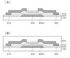
図4(A)のトランジスタはボトムゲートボトムコンタクト型(BGBC)であり、絶
縁表面を有する基板100上に設けられたゲート電極200と、ゲート電極200上に設
けられたゲート絶縁層300と、ゲート絶縁層300上に設けられたコンタクト電極51
0及びコンタクト電極520と、ゲート絶縁層300上及びコンタクト電極510上及び
コンタクト電極520上に設けられた酸化物半導体層410(島状)と、を有するトラン
ジスタである。The transistor of FIG. 4A is a bottom gate bottom contact type (BGBC), and has a
It is a transistor having 0 and a
なお、トランジスタを覆う絶縁層600が設けられている。 An insulating
また、破線8000の部分がバックチャネルになる。 Further, the portion of the
図4(B)のトランジスタはトップゲート型のトランジスタであり、絶縁表面を有する
基板100上に設けられた酸化物半導体層410(島状)と、酸化物半導体層410上に
設けられたゲート絶縁層300と、ゲート絶縁層300上に設けられたゲート電極200
とを有するトランジスタである。The transistor of FIG. 4B is a top gate type transistor, and is an oxide semiconductor layer 410 (island-shaped) provided on a
It is a transistor having and.
なお、トランジスタを覆う絶縁層600が設けられており、前記絶縁層に設けられたコ
ンタクトホールを介して配線810、配線820、配線830が設けられている。An insulating
図4(C)のトランジスタはチャネルストップ型のトランジスタであり、絶縁表面を有
する基板100上に設けられたゲート電極200と、ゲート電極200上に設けられたゲ
ート絶縁層300と、ゲート絶縁層300上に設けられた酸化物半導体層410(島状)
と、酸化物半導体層410上に設けられたチャネル保護層700と、酸化物半導体層41
0上及びチャネル保護層700上に設けられたコンタクト電極510及びコンタクト電極
520と、を有するトランジスタである。The transistor of FIG. 4C is a channel stop type transistor, which is a
, The
It is a transistor having a
なお、トランジスタを覆う絶縁層600が設けられている。 An insulating
また、破線8000の部分がバックチャネルになる。 Further, the portion of the
ここで、チャネル保護層700の材料は、実施の形態1で説明した絶縁層600の材料
と同様の材料を用いることができる。チャネル保護層700と絶縁層600の材料は同じ
でも異なっていても良い。Here, as the material of the
そして、チャネルストップ型のトランジスタにおいてバックチャネルと接する部分は絶
縁層600ではなくチャネル保護層700である。In the channel stop type transistor, the portion in contact with the back channel is not the insulating
よって、チャネル保護層700には水素元素を含む物質の含有量が少ない膜を用いるこ
とが好ましい。Therefore, it is preferable to use a film having a low content of a substance containing a hydrogen element for the
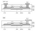
図15(A)のトランジスタはトップゲート型のトランジスタ(TGBC)であり、下
地絶縁層900上に設けられたコンタクト電極510及びコンタクト電極520と、下地
絶縁層900上及びコンタクト電極510上及びコンタクト電極520上に設けられた酸
化物半導体層410(島状)と、酸化物半導体層410上に設けられたゲート絶縁層30
0と、ゲート絶縁層300上に設けられたゲート電極200とを有するトランジスタであ
る。The transistor of FIG. 15A is a top gate type transistor (TGBC), and the
It is a transistor having 0 and a
なお、下地絶縁層900は、基板100上に設けられている。 The
また、トランジスタを覆う絶縁層600が設けられている。 Further, an insulating
また、破線8000の部分がバックチャネルになる。 Further, the portion of the
ここで、下地絶縁層900の材料は、実施の形態1で説明した絶縁層600の材料と同
様の材料を用いることができる。下地絶縁層900と絶縁層600の材料は同じでも異な
っていても良い。Here, as the material of the
そして、トップゲート型のトランジスタにおいてバックチャネルと接する部分は絶縁層
600ではなく下地絶縁層900である。In the top gate type transistor, the portion in contact with the back channel is not the insulating
よって、下地絶縁層900には水素元素を含む物質の含有量が少ない膜を用いることが
好ましい。Therefore, it is preferable to use a film having a low content of a substance containing a hydrogen element for the
また、実施の形態1に記載した方法と同様の方法を用いて、下地絶縁層900を酸素過
剰な絶縁層とすると好ましい。この場合、第1の加熱処理を行うと、酸化物半導体層から
酸素が放出されると同時に、下地絶縁層から酸素が酸化物半導体層に供給されることにな
る。Further, it is preferable that the underlying insulating
図15(B)のトランジスタはトップゲート型のトランジスタ(TGTC)であり、下
地絶縁層900上に設けられた酸化物半導体層410(島状)と、酸化物半導体層410
上及び下地絶縁層900上に設けられたコンタクト電極510及びコンタクト電極520
と、酸化物半導体層上及びコンタクト電極510上及びコンタクト電極520上に設けら
れたゲート絶縁層300と、ゲート絶縁層300上に設けられたゲート電極200とを有
するトランジスタである。The transistor in FIG. 15B is a top gate type transistor (TGTC), and is an oxide semiconductor layer 410 (island-shaped) provided on the underlying insulating
Contact
A transistor having a
なお、下地絶縁層900は、基板100上に設けられている。 The
また、トランジスタを覆う絶縁層600が設けられている。 Further, an insulating
また、破線8000の部分がバックチャネルになる。 Further, the portion of the
ここで、下地絶縁層900の材料は、実施の形態1で説明した絶縁層600の材料と同
様の材料を用いることができる。下地絶縁層900と絶縁層600の材料は同じでも異な
っていても良い。Here, as the material of the
そして、トップゲート型のトランジスタにおいてバックチャネルと接する部分は絶縁層
600ではなく下地絶縁層900である。In the top gate type transistor, the portion in contact with the back channel is not the insulating
よって、下地絶縁層900には水素元素を含む物質の含有量が少ない膜を用いることが
好ましい。Therefore, it is preferable to use a film having a low content of a substance containing a hydrogen element for the
なお、図4(B)のトランジスタでは、チャネル形成領域(ゲート電極と酸化物半導体
層とが重なる領域)と、接触領域(配線と酸化物半導体が接触している領域)と、の間に
数μmのオフセット領域が形成されている。In the transistor of FIG. 4B, the number is between the channel formation region (the region where the gate electrode and the oxide semiconductor layer overlap) and the contact region (the region where the wiring and the oxide semiconductor are in contact). An offset region of μm is formed.
オフセット領域は、トランジスタのオフ電流を下げる点でメリットがあるが、トランジ
スタのオン電流も下げてしまうという点でデメリットがある。The offset region has an advantage in that the off-current of the transistor is reduced, but has a disadvantage in that the on-current of the transistor is also reduced.
一方、図15(A)及び図15(B)では、図4(B)のようなオフセット領域が存在
しないので、図4(B)と比較してトランジスタのオン電流を向上することができるとい
うメリットがある。On the other hand, in FIGS. 15A and 15B, since the offset region as shown in FIG. 4B does not exist, the on-current of the transistor can be improved as compared with FIG. 4B. There are merits.
以上のように、トランジスタはどのような構造でも良い。 As described above, the transistor may have any structure.
つまり、トランジスタは、少なくともゲート電極と、酸化物半導体層と、前記ゲート電
極と前記酸化物半導体層との間に挟まれたゲート絶縁層を有する構造であればどのような
構造を用いても良い。That is, any structure may be used for the transistor as long as it has at least a gate electrode, an oxide semiconductor layer, and a gate insulating layer sandwiched between the gate electrode and the oxide semiconductor layer. ..
また、第1のゲート電極と、第1のゲート電極上の第1のゲート絶縁層と、第1のゲー
ト絶縁層上の酸化物半導体層と、酸化物半導体層上の第2のゲート絶縁層と、第2のゲー
ト絶縁層上の第2のゲート電極と、を有するデュアルゲート型トランジスタを用いても良
い。Further, a first gate electrode, a first gate insulating layer on the first gate electrode, an oxide semiconductor layer on the first gate insulating layer, and a second gate insulating layer on the oxide semiconductor layer. And a dual gate type transistor having a second gate electrode on the second gate insulating layer may be used.
したがって、トランジスタの構造は、実施の形態1及び実施の形態2に列挙した構造に
限定されないことを付言しておく。Therefore, it should be added that the structure of the transistor is not limited to the structures listed in the first and second embodiments.
本実施の形態の内容の一部又は全部は、他の全ての実施の形態及び実施例と組み合わせ
て実施することができる。Part or all of the content of this embodiment may be implemented in combination with all other embodiments and examples.
(実施の形態3)
図4(A)に示す半導体装置の作製方法の一例を示す。(Embodiment 3)
An example of the manufacturing method of the semiconductor device shown in FIG. 4A is shown.
なお、材料、加熱処理条件等は他の実施の形態と同様である。 The materials, heat treatment conditions, etc. are the same as those of the other embodiments.
絶縁表面を有する基板100上にゲート電極200を形成し、ゲート電極200上にゲ
ート絶縁層300を形成し、ゲート絶縁層300上にコンタクト電極510及びコンタク
ト電極520を形成する(図5(A))。A
次に、ゲート絶縁層300上及びコンタクト電極510上及びコンタクト電極520上
に酸化物半導体層400を形成する(図5(B))。Next, the
次に、酸化物半導体層の第1の加熱処理を行う。 Next, the first heat treatment of the oxide semiconductor layer is performed.
第1の加熱処理の条件は実施の形態1と同様である。 The conditions of the first heat treatment are the same as those of the first embodiment.
第1の加熱処理は酸化物半導体層400を島状にエッチングして酸化物半導体層410
を形成した後に行っても良い。In the first heat treatment, the
It may be done after forming.
しかしながら、島状にエッチングして酸化物半導体層410を形成した後であると、コ
ンタクト電極が露出している。However, after etching in an island shape to form the
コンタクト電極が露出した状態で第1の加熱処理を行うとコンタクト電極表面が酸化し
て表面の導電性が低下する。When the first heat treatment is performed with the contact electrode exposed, the surface of the contact electrode is oxidized and the conductivity of the surface is lowered.
よって、コンタクト電極が酸化物半導体層400で覆われた状態で第1の加熱処理を行
うことが好ましい。Therefore, it is preferable to perform the first heat treatment with the contact electrode covered with the
次に、酸化物半導体層400を島状にエッチングして酸化物半導体層410を形成し、
トランジスタを覆う絶縁層600を形成する(図5(C))。Next, the
An insulating
なお、破線8000の部分がバックチャネルとなる。 The portion of the
図5(C)の工程の後、絶縁層600にコンタクトホールを形成し、絶縁層600上に
配線810、配線820等を形成しても良い(図6(A))。After the step of FIG. 5C, a contact hole may be formed in the insulating
図5(C)の工程の後、絶縁層600にコンタクトホールを形成し、絶縁層600上に
画素電極910を形成しても良い(図6(B))。After the step of FIG. 5C, a contact hole may be formed in the insulating
図6(A)のように絶縁層600上に配線を形成した後、配線上に更に絶縁層、配線、
トランジスタ、表示素子、又はアンテナ等を形成しても良い。After forming the wiring on the insulating
Transistors, display elements, antennas, and the like may be formed.
図6(B)のように画素電極910を形成した後、表示素子(EL素子、液晶素子等)
を形成することによって、表示装置を形成することができる。After forming the
By forming the display device, a display device can be formed.
また、図6(A)の工程又は図6(B)の工程の後、第2の加熱処理を行うことが好ま
しい。Further, it is preferable to perform the second heat treatment after the step of FIG. 6A or the step of FIG. 6B.
なお、図5(C)の工程と、図6(A)の工程又は図6(B)の工程と、の間に第2の
加熱処理を行っても良い。A second heat treatment may be performed between the step of FIG. 5 (C) and the step of FIG. 6 (A) or the step of FIG. 6 (B).
第2の加熱処理の条件は実施の形態1と同様である。 The conditions for the second heat treatment are the same as those in the first embodiment.
本実施の形態の内容の一部又は全部は、他の全ての実施の形態及び実施例と組み合わせ
て実施することができる。Part or all of the content of this embodiment may be implemented in combination with all other embodiments and examples.
(実施の形態4)
図4(C)に示す半導体装置の作製方法の一例を示す。(Embodiment 4)
An example of the manufacturing method of the semiconductor device shown in FIG. 4C is shown.
なお、材料、加熱処理条件等は他の実施の形態と同様である。 The materials, heat treatment conditions, etc. are the same as those of the other embodiments.
まず、実施の形態1と同様に図1(B)の構造を形成する。 First, the structure of FIG. 1B is formed in the same manner as in the first embodiment.
なお、実施の形態1と同様に第1の加熱処理もおこなっておく。 The first heat treatment is also performed in the same manner as in the first embodiment.
次に、チャネル保護層700(島状)を形成し、チャネル保護層を覆う導電層500を
形成する(図7(A))。Next, the channel protection layer 700 (island-shaped) is formed, and the
次に、導電層500をエッチングしてコンタクト電極510及びコンタクト電極520
を形成する(図7(B))。Next, the
(Fig. 7 (B)).
なお、破線8000の部分がバックチャネルである。 The portion of the
そして、チャネル保護層700が存在することによって、コンタクト電極形成時にバッ
クチャネルがエッチングされないため、バックチャネルのダメージを低減することができ
る。Since the back channel is not etched when the contact electrode is formed due to the presence of the
ここで、チャネル保護層700の材料は、実施の形態1で説明した絶縁層600の材料
と同様の材料を用いることができる。チャネル保護層700と絶縁層600の材料は同じ
でも異なっていても良い。Here, as the material of the
そして、チャネルストップ型のトランジスタにおいてバックチャネルと接する部分は絶
縁層600ではなくチャネル保護層700である。In the channel stop type transistor, the portion in contact with the back channel is not the insulating
よって、チャネル保護層700は水素元素を含む物質の含有量が少ない膜を用いること
が好ましい。Therefore, it is preferable to use a film having a low content of a substance containing a hydrogen element for the
また、実施の形態1に記載した方法と同様の方法を用いて、チャネル保護層700を酸
素過剰な絶縁層とすると好ましい。Further, it is preferable to use the same method as that described in the first embodiment to make the
次に、トランジスタを覆う絶縁層600を形成する(図7(C))。 Next, the insulating
図7(C)の工程の後、絶縁層600にコンタクトホールを形成し、絶縁層600上に
配線810、配線820等を形成しても良い(図8(A))。After the step of FIG. 7C, a contact hole may be formed in the insulating
図7(C)の工程の後、絶縁層600にコンタクトホールを形成し、絶縁層600上に
画素電極910を形成しても良い(図8(B))。After the step of FIG. 7C, a contact hole may be formed in the insulating
図8(A)のように絶縁層600上に配線を形成した後、配線上に更に絶縁層、配線、
トランジスタ、表示素子、又はアンテナ等を形成しても良い。After forming the wiring on the insulating
Transistors, display elements, antennas, and the like may be formed.
図8(B)のように画素電極910を形成した後、表示素子(EL素子、液晶素子等)
を形成すると表示装置を形成することができる。After forming the
A display device can be formed by forming.
また、図8(A)の工程又は図8(B)の工程の後、第2の加熱処理を行うことが好ま
しい。Further, it is preferable to perform the second heat treatment after the step of FIG. 8A or the step of FIG. 8B.
なお、図7(C)の工程と、図8(A)の工程又は図8(B)の工程と、の間に第2の
加熱処理を行っても良い。A second heat treatment may be performed between the step of FIG. 7 (C) and the step of FIG. 8 (A) or the step of FIG. 8 (B).
第2の加熱処理の条件は実施の形態1と同様である。 The conditions for the second heat treatment are the same as those in the first embodiment.
本実施の形態の内容の一部又は全部は、他の全ての実施の形態及び実施例と組み合わせ
て実施することができる。Part or all of the content of this embodiment may be implemented in combination with all other embodiments and examples.
(実施の形態5)
半導体装置としては、各種集積回路がある。(Embodiment 5)
As a semiconductor device, there are various integrated circuits.
例えば、表示装置(液晶表示装置、エレクトロルミネッセンス表示装置(発光装置)等
)、アンテナを介して無線通信を行う半導体装置(RFIDタグ、無線タグ、ICチップ
、無線チップ、非接触信号処理装置、半導体集積回路チップ)等があるが、これらに限定
されない。For example, display devices (liquid crystal display devices, electroluminescence display devices (light emitting devices), etc.), semiconductor devices that perform wireless communication via antennas (RFID tags, wireless tags, IC chips, wireless chips, non-contact signal processing devices, semiconductors). Integrated circuit chips), etc., but are not limited to these.
本実施の形態の内容の一部又は全部は、他の全ての実施の形態及び実施例と組み合わせ
て実施することができる。Part or all of the content of this embodiment may be implemented in combination with all other embodiments and examples.
酸化物半導体中の窒素濃度の影響を調査した。 The effect of nitrogen concentration in oxide semiconductors was investigated.
まず、ガラス基板上に酸化物半導体層を形成した。 First, an oxide semiconductor layer was formed on a glass substrate.
そして、酸化物半導体層形成後に加熱処理を行っていない場合と、酸化物半導体層形成
後に加熱処理を行った場合と、を比較した。Then, the case where the heat treatment was not performed after the formation of the oxide semiconductor layer and the case where the heat treatment was performed after the formation of the oxide semiconductor layer were compared.
比較方法は二次イオン質量分析法(SIMS:Secondary Ion Mass
Spectrometry)を用いた。The comparison method is secondary ion mass spectrometry (SIMS: Secondary Ion Mass).
Spectrometery) was used.
なお、加熱処理は350℃、1時間とした。 The heat treatment was 350 ° C. for 1 hour.
加熱雰囲気は大気雰囲気又は窒素雰囲気とした。 The heating atmosphere was an atmospheric atmosphere or a nitrogen atmosphere.
ここで、酸化物半導体層は、In:Ga:Znが1:1:0.5(原子比)(In2O
3:Ga2O3:ZnOが1:1:1(モル比))の酸化物半導体ターゲットをスパッタ
して形成した。Here, in the oxide semiconductor layer, In: Ga: Zn is 1: 1: 0.5 (atomic ratio) (In2 O).
3 : Ga2 O3 : ZnO was formed by sputtering an oxide semiconductor target having a ratio of 1: 1: 1 (molar ratio).
なお、酸化物半導体層の成膜前に、成膜室のリークの低減、成膜室の内壁の窒素の低減
、ダミー基板への成膜等を充分行い窒素が酸化物半導体層中に混入することを徹底的に排
除した。Before the oxide semiconductor layer is formed, the leakage in the film forming chamber is reduced, the nitrogen in the inner wall of the film forming chamber is reduced, the film is formed on the dummy substrate, and the nitrogen is mixed in the oxide semiconductor layer. Thoroughly eliminated that.
(サンプル1)
スパッタガスの流量がAr/N2=40/0sccm(N2割合0%)のサンプルをサ
ンプル1とした。なお、サンプル1は3つ用意した。(Sample 1)
A sample having a sputter gas flow rate of Ar / N2 = 40/0 sccm (N2 ratio 0%) was used as
サンプル1のSIMSの測定結果を図10に示す。 The measurement result of SIMS of
(サンプル2)
スパッタガスの流量がAr/N2=35/5sccm(N2割合12.5%)のサンプ
ルをサンプル2とした。なお、サンプル2は3つ用意した。(Sample 2)
A sample having a sputter gas flow rate of Ar / N2 = 35/5 sccm (N2 ratio 12.5%) was used as sample 2. Three samples 2 were prepared.
サンプル2のSIMSの測定結果を図11に示す。 The measurement result of SIMS of sample 2 is shown in FIG.
(サンプル3)
スパッタガスの流量がAr/N2=0/40sccm(N2割合100%)のサンプル
をサンプル3とした。なお、サンプル3は3つ用意した。(Sample 3)
A sample having a sputter gas flow rate of Ar / N2 = 0/40 sccm (N2 ratio 100%) was used as sample 3. Three samples 3 were prepared.
サンプル3のSIMSの測定結果を図12に示す。 The measurement result of SIMS of sample 3 is shown in FIG.
(考察)
図10~図12において、点線3001が加熱処理を行っていないサンプル(as-d
epo)、太い実線3002が窒素雰囲気で加熱したサンプル(N2ベーク)、細い実線
3003が大気雰囲気で加熱したサンプル(大気ベーク)を示している。(Discussion)
In FIGS. 10 to 12, the dotted
epo), the thick
また、図10~図12において、(A)は水素濃度であり、(B)は窒素濃度である。 Further, in FIGS. 10 to 12, (A) is a hydrogen concentration and (B) is a nitrogen concentration.
図10~図12において、縦軸は濃度であり、横軸は酸化物半導体層表面からの深さ(
膜厚)である。In FIGS. 10 to 12, the vertical axis is the concentration and the horizontal axis is the depth from the surface of the oxide semiconductor layer (
Film thickness).
なお、二次イオン質量分析法(SIMS)の測定結果には有効範囲がある。 The measurement results of the secondary ion mass spectrometry (SIMS) have an effective range.
そして、本実施例の場合、酸化物半導体層の表面付近(図10~図12だと深さが0n
m~30nm付近)及び酸化物半導体層とガラス基板との界面付近(図10~図12だと
深さが80nm~100nm付近)について正確な値を算出しにくくなっている。Then, in the case of this embodiment, the depth is 0 n near the surface of the oxide semiconductor layer (FIGS. 10 to 12 show that the depth is 0 n).
It is difficult to calculate an accurate value for the vicinity of the interface between the oxide semiconductor layer and the glass substrate (around m to 30 nm) and the vicinity of the interface (the depth is around 80 nm to 100 nm in FIGS. 10 to 12).
したがって、本実施例の場合は、深さが30nm~80nmの範囲をSIMSの測定結
果の有効範囲とした。Therefore, in the case of this example, the range of the depth of 30 nm to 80 nm was set as the effective range of the SIMS measurement result.
ここで、図10(A)の点線3001(as-depo)、図11(A)の点線300
1(as-depo)、及び図12(A)の点線3001(as-depo)の有効範囲
における水素濃度の平均値を比較すると、図11(A)の方が図10(A)よりも高く、
図12(A)の方が図11(A)よりも高いことがわかる。Here, the dotted line 3001 (as-depo) in FIG. 10 (A) and the dotted
Comparing the average values of hydrogen concentrations in the effective range of 1 (as-depo) and the dotted line 3001 (as-depo) in FIG. 12 (A), FIG. 11 (A) is higher than FIG. 10 (A). ,
It can be seen that FIG. 12 (A) is higher than FIG. 11 (A).
さらに、図10(B)の点線3001(as-depo)、図11(B)の点線300
1(as-depo)、及び図12(B)の点線3001(as-depo)の有効範囲
における窒素濃度の平均値を比較すると、図11(B)の方が図10(B)よりも高く、
図12(B)の方が図11(B)よりも高いことがわかる。Further, the dotted line 3001 (as-depo) in FIG. 10 (B) and the dotted
Comparing the average values of nitrogen concentrations in the effective range of 1 (as-depo) and the dotted line 3001 (as-depo) in FIG. 12 (B), FIG. 11 (B) is higher than that in FIG. 10 (B). ,
It can be seen that FIG. 12 (B) is higher than FIG. 11 (B).
つまり、as-depo条件において、酸化物半導体層中の窒素濃度が多いほど、酸化
物半導体層中の水素濃度が多くなることがわかる。That is, it can be seen that, under the as-depo condition, the higher the nitrogen concentration in the oxide semiconductor layer, the higher the hydrogen concentration in the oxide semiconductor layer.
したがって、酸化物半導体層中の窒素濃度が多いほど、酸化物半導体層中に水素が混入
しやすくなることがわかった。Therefore, it was found that the higher the nitrogen concentration in the oxide semiconductor layer, the easier it is for hydrogen to be mixed in the oxide semiconductor layer.
また、図10(A)を参照すると加熱処理を行うことによって水素濃度が低下している
ことがわかる。Further, referring to FIG. 10A, it can be seen that the hydrogen concentration is reduced by performing the heat treatment.
一方、図11(A)、図12(A)を参照すると加熱処理を行うことによって水素濃度
が上昇していることがわかる。On the other hand, referring to FIGS. 11 (A) and 12 (A), it can be seen that the hydrogen concentration is increased by performing the heat treatment.
なお、図12(A)において、30nm~60nmの範囲では点線3001(as-d
epo)、太い実線3002(N2ベーク)、細い実線3003(大気ベーク)の水素濃
度にあまり差がない。In FIG. 12A, the dotted line 3001 (as-d) is in the range of 30 nm to 60 nm.
There is not much difference in hydrogen concentration between epo), thick solid line 3002 (N2 bake), and thin solid line 3003 (atmospheric bake).
しかしながら、有効範囲である30nm~80nmでの水素濃度の平均値は、太い実線
3002(N2ベーク)及び細い実線3003(大気ベーク)の方が、点線3001(a
s-depo)よりも高い。However, the average value of the hydrogen concentration in the effective range of 30 nm to 80 nm is the dotted line 3001 (a) for the thick solid line 3002 (N2 bake) and the thin solid line 3003 (atmospheric bake).
Higher than s-depo).
よって、酸化物半導体層中の水素の総量を比較した場合、太い実線3002(N2ベー
ク)及び細い実線3003(大気ベーク)の方が、点線3001(as-depo)より
も多いことは明らかである。Therefore, when comparing the total amount of hydrogen in the oxide semiconductor layer, it is clear that the thick solid line 3002 (N2 bake) and the thin solid line 3003 (atmospheric bake) are larger than the dotted line 3001 (as-depo). be.
また、図12(A)において、太い実線3002(N2ベーク)及び細い実線3003
(大気ベーク)の形状がV字のような形になった理由は、膜表面及びガラス基板から水素
が注入されたためであると考察した。Further, in FIG. 12A, a thick solid line 3002 (N2 bake) and a thin
It was considered that the reason why the shape of (atmospheric bake) became V-shaped was that hydrogen was injected from the film surface and the glass substrate.
ここで、サンプル1において、SIMSの測定結果の有効範囲における窒素濃度の最大
値は、1×10²⁰atoms/cm3以下(1×1020atoms/cm3未満)で
あった。(図10(B))Here, in
よって、サンプル1において、SIMSの測定結果の有効範囲における窒素濃度の平均
値も1×10²⁰atoms/cm3以下(1×1020atoms/cm3未満)であ
った(平均値が最大値より大きな値になることはない)。Therefore, in
なお、サンプル1のas-depo条件(図10)において、SIMSの測定結果の有
効範囲における窒素濃度の最大値は9.3×10¹⁹atoms/cm3であり、SIM
Sの測定結果の有効範囲における窒素濃度の最小値は1.9×10¹⁹atoms/cm
3であり、SIMSの測定結果の有効範囲における窒素濃度の平均値は6.1×10¹⁹
atoms/cm3であった。In the as-depo condition (FIG. 10) of the
The minimum value of nitrogen concentration in the effective range of the measurement result of S is 1.9 × 10¹⁹ atoms / cm.
3 and the average value of nitrogen concentration in the effective range of SIMS measurement results is 6.1 × 10¹⁹
It was atoms / cm3 .
また、サンプル1のas-depo条件(図10)において、SIMSの測定結果の有
効範囲における水素濃度の最大値は6.9×10¹⁹atoms/cm3であり、SIM
Sの測定結果の有効範囲における水素濃度の最小値は4.5×10¹⁹atoms/cm
3であり、SIMSの測定結果の有効範囲における水素濃度の平均値は5.6×10¹⁹
atoms/cm3であった。Further, under the as-depo condition (FIG. 10) of the
The minimum value of hydrogen concentration in the effective range of the measurement result of S is 4.5 × 10¹⁹ atoms / cm.
3 and the average value of hydrogen concentration in the effective range of SIMS measurement results is 5.6 × 10¹⁹
It was atoms / cm3 .
また、サンプル1のN2ベーク条件(図10)において、SIMSの測定結果の有効範
囲における窒素濃度の最大値は9.7×10¹⁹atoms/cm3であり、SIMSの
測定結果の有効範囲における窒素濃度の最小値は3.0×10¹⁹atoms/cm3で
あり、SIMSの測定結果の有効範囲における窒素濃度の平均値は6.0×10¹⁹at
oms/cm3であった。Further, under the N2 baking condition of sample 1 (FIG. 10), the maximum value of the nitrogen concentration in the effective range of the SIMS measurement result is 9.7 × 10¹⁹ atoms / cm3 , which is the effective range of the SIMS measurement result. The minimum value of nitrogen concentration is 3.0 × 10¹⁹ atoms / cm3 , and the average value of nitrogen concentration in the effective range of SIMS measurement results is 6.0 × 10¹⁹ at.
It was oms / cm3 .
また、サンプル1のN2ベーク条件(図10)において、SIMSの測定結果の有効範
囲における水素濃度の最大値は2.3×10¹⁹atoms/cm3であり、SIMSの
測定結果の有効範囲における水素濃度の最小値は6.4×10¹⁸atoms/cm3で
あり、SIMSの測定結果の有効範囲における水素濃度の平均値は1.2×10¹⁹at
oms/cm3であった。Further, under the N2 baking condition of sample 1 (FIG. 10), the maximum value of the hydrogen concentration in the effective range of the SIMS measurement result is 2.3 × 10¹⁹ atoms / cm3 , which is the effective range of the SIMS measurement result. The minimum value of hydrogen concentration is 6.4 × 10¹⁸ atoms / cm3 , and the average value of hydrogen concentration in the effective range of SIMS measurement results is 1.2 × 10¹⁹ at.
It was oms / cm3 .
また、サンプル1の大気ベーク条件(図10)において、SIMSの測定結果の有効範
囲における窒素濃度の最大値は3.1×10¹⁹atoms/cm3であり、SIMSの
測定結果の有効範囲における窒素濃度の最小値は4.4×10¹⁸atoms/cm3で
あり、SIMSの測定結果の有効範囲における窒素濃度の平均値は1.8×10¹⁹at
oms/cm3であった。Further, under the atmospheric baking conditions of sample 1 (FIG. 10), the maximum value of the nitrogen concentration in the effective range of the SIMS measurement result is 3.1 × 10¹⁹ atoms / cm3 , and the nitrogen in the effective range of the SIMS measurement result. The minimum concentration is 4.4 × 10¹⁸ atoms / cm3 , and the average value of nitrogen concentration in the effective range of SIMS measurement results is 1.8 × 10¹⁹ at.
It was oms / cm3 .
また、サンプル1の大気ベーク条件(図10)において、SIMSの測定結果の有効範
囲における水素濃度の最大値は6.7×10¹⁸atoms/cm3であり、SIMSの
測定結果の有効範囲における水素濃度の最小値は2.0×10¹⁸atoms/cm3で
あり、SIMSの測定結果の有効範囲における水素濃度の平均値は3.8×10¹⁸at
oms/cm3であった。Further, under the atmospheric baking conditions of Sample 1 (FIG. 10), the maximum value of the hydrogen concentration in the effective range of the SIMS measurement result is 6.7 × 10¹⁸ atoms / cm3 , and the hydrogen in the effective range of the SIMS measurement result. The minimum concentration is 2.0 × 10¹⁸ atoms / cm3 , and the average hydrogen concentration in the effective range of SIMS measurement results is 3.8 × 10¹⁸ at.
It was oms / cm3 .
一方、サンプル2及びサンプル3において、SIMSの測定結果の有効範囲における窒
素濃度の最小値は、1×10²²atoms/cm3以上であった(図11(B)、図1
2(B))。On the other hand, in Samples 2 and 3, the minimum value of nitrogen concentration in the effective range of SIMS measurement results was 1 × 10²² atoms / cm3 or more (FIG. 11 (B), FIG. 1).
2 (B)).
よって、サンプル2及びサンプル3において、SIMSの測定結果の有効範囲における
窒素濃度の平均値も、1×10²²atoms/cm3以上であった(平均値が最小値よ
り小さな値になることはない)。Therefore, in Samples 2 and 3, the average value of the nitrogen concentration in the effective range of the SIMS measurement results was also 1 × 10²² atoms / cm3 or more (the average value is never smaller than the minimum value). ).
なお、サンプル2のas-depo条件(図11)において、SIMSの測定結果の有
効範囲における窒素濃度の最大値は1.6×10²²atoms/cm3であり、SIM
Sの測定結果の有効範囲における窒素濃度の最小値は1.5×10²²atoms/cm
3であり、SIMSの測定結果の有効範囲における窒素濃度の平均値は1.5×10²²
atoms/cm3であった。In the as-depo condition (FIG. 11) of the sample 2, the maximum value of the nitrogen concentration in the effective range of the SIMS measurement result is 1.6 × 10²² atoms / cm3 , which is SIM.
The minimum value of nitrogen concentration in the effective range of the measurement result of S is 1.5 × 10²² atoms / cm.
3 and the average value of nitrogen concentration in the effective range of SIMS measurement results is 1.5 × 10²²
It was atoms / cm3 .
また、サンプル2のas-depo条件(図11)において、SIMSの測定結果の有
効範囲における水素濃度の最大値は1.0×10²⁰atoms/cm3であり、SIM
Sの測定結果の有効範囲における水素濃度の最小値は6.3×10¹⁹atoms/cm
3であり、SIMSの測定結果の有効範囲における水素濃度の平均値は7.8×10¹⁹
atoms/cm3であった。Further, under the as-depo condition (FIG. 11) of the sample 2, the maximum value of the hydrogen concentration in the effective range of the SIMS measurement result is 1.0 × 10²⁰ atoms / cm3 , which is SIM.
The minimum value of hydrogen concentration in the effective range of the measurement result of S is 6.3 × 10¹⁹ atoms / cm.
3 and the average value of hydrogen concentration in the effective range of SIMS measurement results is 7.8 × 10¹⁹
It was atoms / cm3 .
また、サンプル2のN2ベーク条件(図11)において、SIMSの測定結果の有効範
囲における窒素濃度の最大値は1.5×10²²atoms/cm3であり、SIMSの
測定結果の有効範囲における窒素濃度の最小値は1.4×10²²atoms/cm3で
あり、SIMSの測定結果の有効範囲における窒素濃度の平均値は1.5×10²²at
oms/cm3であった。Further, under the N2 baking condition of sample 2 (FIG. 11), the maximum value of the nitrogen concentration in the effective range of the SIMS measurement result is 1.5 × 10²² atoms / cm3 , which is the effective range of the SIMS measurement result. The minimum value of nitrogen concentration is 1.4 × 10²² atoms / cm3 , and the average value of nitrogen concentration in the effective range of SIMS measurement results is 1.5 × 10²² at.
It was oms / cm3 .
また、サンプル2のN2ベーク条件(図11)において、SIMSの測定結果の有効範
囲における水素濃度の最大値は1.2×10²¹atoms/cm3であり、SIMSの
測定結果の有効範囲における水素濃度の最小値は6.5×10²⁰atoms/cm3で
あり、SIMSの測定結果の有効範囲における水素濃度の平均値は7.7×10²⁰at
oms/cm3であった。Further, under the N2 baking condition of sample 2 (FIG. 11), the maximum value of the hydrogen concentration in the effective range of the SIMS measurement result is 1.2 × 10²¹ atoms / cm3 , which is the effective range of the SIMS measurement result. The minimum value of hydrogen concentration is 6.5 × 10²⁰ atoms / cm3 , and the average value of hydrogen concentration in the effective range of SIMS measurement results is 7.7 × 10²⁰ at.
It was oms / cm3 .
また、サンプル2の大気ベーク条件(図11)において、SIMSの測定結果の有効範
囲における窒素濃度の最大値は1.6×10²²atoms/cm3であり、SIMSの
測定結果の有効範囲における窒素濃度の最小値は1.5×10²²atoms/cm3で
あり、SIMSの測定結果の有効範囲における窒素濃度の平均値は1.6×10²²at
oms/cm3であった。Further, under the atmospheric baking conditions of sample 2 (FIG. 11), the maximum value of the nitrogen concentration in the effective range of the SIMS measurement result is 1.6 × 10²² atoms / cm3 , and the nitrogen in the effective range of the SIMS measurement result. The minimum concentration is 1.5 × 10²² atoms / cm3 , and the average nitrogen concentration in the effective range of SIMS measurement results is 1.6 × 10²² at.
It was oms / cm3 .
また、サンプル2の大気ベーク条件(図11)において、SIMSの測定結果の有効範
囲における水素濃度の最大値は6.9×10²⁰atoms/cm3であり、SIMSの
測定結果の有効範囲における水素濃度の最小値は4.4×10²⁰atoms/cm3で
あり、SIMSの測定結果の有効範囲における水素濃度の平均値は5.3×10²⁰at
oms/cm3であった。Further, in the atmospheric baking condition of sample 2 (FIG. 11), the maximum value of the hydrogen concentration in the effective range of the SIMS measurement result is 6.9 × 10²⁰ atoms / cm3 , and the hydrogen in the effective range of the SIMS measurement result. The minimum concentration is 4.4 × 10²⁰ atoms / cm3 , and the average hydrogen concentration in the effective range of SIMS measurement results is 5.3 × 10²⁰ at.
It was oms / cm3 .
また、サンプル3のas-depo条件(図12)において、SIMSの測定結果の有
効範囲における窒素濃度の最大値は3.4×10²²atoms/cm3であり、SIM
Sの測定結果の有効範囲における窒素濃度の最小値は3.1×10²²atoms/cm
3であり、SIMSの測定結果の有効範囲における窒素濃度の平均値は3.3×10²²
atoms/cm3であった。Further, under the as-depo condition (FIG. 12) of the sample 3, the maximum value of the nitrogen concentration in the effective range of the SIMS measurement result is 3.4 × 10²² atoms / cm3 , which is SIM.
The minimum value of nitrogen concentration in the effective range of the measurement result of S is 3.1 × 10²² atoms / cm.
3 and the average value of nitrogen concentration in the effective range of SIMS measurement results is 3.3 × 10²² .
It was atoms / cm3 .
また、サンプル3のas-depo条件(図12)において、SIMSの測定結果の有
効範囲における水素濃度の最大値は1.9×10²⁰atoms/cm3であり、SIM
Sの測定結果の有効範囲における水素濃度の最小値は1.1×10²⁰atoms/cm
3であり、SIMSの測定結果の有効範囲における水素濃度の平均値は1.4×10²⁰
atoms/cm3であった。Further, under the as-depo condition (FIG. 12) of the sample 3, the maximum value of the hydrogen concentration in the effective range of the SIMS measurement result is 1.9 × 10²⁰ atoms / cm3 , which is SIM.
The minimum value of hydrogen concentration in the effective range of the measurement result of S is 1.1 × 10²⁰ atoms / cm.
3 and the average value of hydrogen concentration in the effective range of SIMS measurement results is 1.4 × 10²⁰
It was atoms / cm3 .
また、サンプル3のN2ベーク条件(図12)において、SIMSの測定結果の有効範
囲における窒素濃度の最大値は3.3×10²²atoms/cm3であり、SIMSの
測定結果の有効範囲における窒素濃度の最小値は3.2×10²²atoms/cm3で
あり、SIMSの測定結果の有効範囲における窒素濃度の平均値は3.2×10²²at
oms/cm3であった。Further, under the N2 baking condition of sample 3 (FIG. 12), the maximum value of the nitrogen concentration in the effective range of the SIMS measurement result is 3.3 × 10²² atoms / cm3 , which is the effective range of the SIMS measurement result. The minimum value of nitrogen concentration is 3.2 × 10²² atoms / cm3 , and the average value of nitrogen concentration in the effective range of SIMS measurement results is 3.2 × 10²² at.
It was oms / cm3 .
また、サンプル3のN2ベーク条件(図12)において、SIMSの測定結果の有効範
囲における水素濃度の最大値は8.6×10²⁰atoms/cm3であり、SIMSの
測定結果の有効範囲における水素濃度の最小値は1.4×10²⁰atoms/cm3で
あり、SIMSの測定結果の有効範囲における水素濃度の平均値は2.7×10²⁰at
oms/cm3であった。Further, under the N2 baking condition of sample 3 (FIG. 12), the maximum value of the hydrogen concentration in the effective range of the SIMS measurement result is 8.6 × 10²⁰ atoms / cm3 , which is the effective range of the SIMS measurement result. The minimum value of hydrogen concentration is 1.4 × 10²⁰ atoms / cm3 , and the average value of hydrogen concentration in the effective range of SIMS measurement results is 2.7 × 10²⁰ at.
It was oms / cm3 .
また、サンプル3の大気ベーク条件(図12)において、SIMSの測定結果の有効範
囲における窒素濃度の最大値は3.5×10²²atoms/cm3であり、SIMSの
測定結果の有効範囲における窒素濃度の最小値は3.3×10²²atoms/cm3で
あり、SIMSの測定結果の有効範囲における窒素濃度の平均値は3.4×10²²at
oms/cm3であった。Further, in the atmospheric baking condition of sample 3 (FIG. 12), the maximum value of the nitrogen concentration in the effective range of the SIMS measurement result is 3.5 × 10²² atoms / cm3 , and the nitrogen in the effective range of the SIMS measurement result. The minimum concentration is 3.3 × 10²² atoms / cm3 , and the average value of nitrogen concentration in the effective range of SIMS measurement results is 3.4 × 10²² at.
It was oms / cm3 .
また、サンプル3の大気ベーク条件(図12)において、SIMSの測定結果の有効範
囲における水素濃度の最大値は1.0×10²¹atoms/cm3であり、SIMSの
測定結果の有効範囲における水素濃度の最小値は7.6×10¹⁹atoms/cm3で
あり、SIMSの測定結果の有効範囲における水素濃度の平均値は2.8×10²⁰at
oms/cm3であった。Further, in the atmospheric baking condition of sample 3 (FIG. 12), the maximum value of the hydrogen concentration in the effective range of the SIMS measurement result is 1.0 × 10²¹ atoms / cm3 , and the hydrogen in the effective range of the SIMS measurement result. The minimum concentration is 7.6 × 10¹⁹ atoms / cm3 , and the average value of hydrogen concentration in the effective range of SIMS measurement results is 2.8 × 10²⁰ at.
It was oms / cm3 .
以上のように、窒素を含有した酸化物半導体層は水素を取り込みやすい性質を有してい
ることがわかった。As described above, it was found that the nitrogen-containing oxide semiconductor layer has a property of easily taking in hydrogen.
逆にいえば、SIMSの測定結果の有効範囲における窒素濃度の平均値が1×10²⁰
atoms/cm3以下(1×1020atoms/cm3未満)である酸化物半導体層
は、水素に対して緻密な層であるといえる。Conversely, the average value of nitrogen concentration in the effective range of SIMS measurement results is 1 × 10²⁰ .
It can be said that the oxide semiconductor layer having atoms / cm3 or less (1 × 10²⁰ atoms / cm3 or less) is a dense layer with respect to hydrogen.
また、サンプル1乃至3において、加熱処理を行っても酸化物半導体層中の窒素濃度は
増加しなかった。サンプル1において大気ベークを行ったものでは酸化物半導体層中の窒
素濃度は減少していた。Further, in
ここで、酸化物半導体層中に窒素が取り込まれるメカニズムは、酸化物半導体層の成膜
時において酸化物半導体層中の酸素結合の一部が切れてしまい、切れた結合の位置に窒素
結合が形成されるためであると推測した。Here, the mechanism by which nitrogen is taken into the oxide semiconductor layer is that a part of the oxygen bond in the oxide semiconductor layer is broken at the time of film formation of the oxide semiconductor layer, and the nitrogen bond is formed at the position of the broken bond. I speculated that it was because it was formed.
よって、切れた結合の位置に酸素結合が形成されれば、酸化物半導体層中に取り込まれ
る窒素濃度を低減できるという仮説を立てた。なお、この推測及び仮説が正しければ、I
n-Ga-Zn-O系以外の酸化物半導体においても窒素は影響を及ぼすことになる。Therefore, it was hypothesized that the concentration of nitrogen incorporated into the oxide semiconductor layer could be reduced if an oxygen bond was formed at the position of the broken bond. If this guess and hypothesis are correct, I
Nitrogen also has an effect on oxide semiconductors other than the n—Ga—Zn—O system.
実施例1の推測及び仮説が正しいか実証するためにスパッタガスに酸素を用いて酸化物
半導体層を形成した。An oxide semiconductor layer was formed by using oxygen as a sputtering gas in order to prove whether the guess and hypothesis of Example 1 were correct.
酸素を供給すれば切れた結合の位置に酸素結合が形成される確率が上がるはずである。 Supplying oxygen should increase the probability that an oxygen bond will be formed at the location of the broken bond.
酸化物半導体層は、In:Ga:Znが1:1:0.5(原子比)(In2O3:Ga
2O3:ZnOが1:1:1(モル比))の酸化物半導体ターゲットをスパッタして形成
した。In the oxide semiconductor layer, In: Ga: Zn is 1: 1: 0.5 (atomic ratio) (In2 O3 : Ga).
It was formed by sputtering an oxide semiconductor target having2 O3 : ZnO of 1: 1: 1 (molar ratio).
なお、酸化物半導体層の成膜前に、成膜室のリークの低減、成膜室の内壁の窒素の低減
、ダミー基板への成膜等を充分行い窒素が酸化物半導体層中に混入することを徹底的に排
除した。Before the oxide semiconductor layer is formed, the leakage in the film forming chamber is reduced, the nitrogen in the inner wall of the film forming chamber is reduced, the film is formed on the dummy substrate, and the nitrogen is mixed in the oxide semiconductor layer. Thoroughly eliminated that.
(サンプル4)
スパッタガスの流量がAr/O2=30/15sccm(O2割合33.3%)のサン
プルをサンプル4(as-depo)とした。(Sample 4)
A sample having a sputter gas flow rate of Ar / O2 = 30/15 sccm (O2 ratio 33.3%) was used as sample 4 (as-depo).
サンプル4のSIMSの測定結果(窒素)を図13(A)に示す。 The SIMS measurement result (nitrogen) of sample 4 is shown in FIG. 13 (A).
(サンプル5)
スパッタガスの流量がAr/O2=0/40sccm(O2割合100%)のサンプル
をサンプル5(as-depo)とした。(Sample 5)
A sample having a sputter gas flow rate of Ar / O2 = 0/40 sccm (O2 ratio 100%) was used as sample 5 (as-depo).
サンプル5のSIMSの測定結果(窒素)を図13(B)に示す。 The SIMS measurement result (nitrogen) of sample 5 is shown in FIG. 13 (B).
(考察)
SIMSの測定結果の有効範囲は実施例1と同じである。(Discussion)
The effective range of the SIMS measurement results is the same as in Example 1.
ここで、サンプル4(図13(A))において、SIMSの測定結果の有効範囲におけ
る窒素濃度の最大値は、5×10¹⁹atoms/cm3以下(5×1019atoms
/cm3未満)である。Here, in sample 4 (FIG. 13 (A)), the maximum value of the nitrogen concentration in the effective range of the SIMS measurement result is 5 × 10¹⁹ atoms / cm3 or less (5 × 10¹⁹ atoms).
/ Cm less than3 ).
よって、サンプル4(図13(A))において、SIMSの測定結果の有効範囲におけ
る窒素濃度の平均値も5×10¹⁹atoms/cm3以下(5×1019atoms/
cm3未満)である(平均値が最大値より大きな値になることはない)。Therefore, in sample 4 (FIG. 13 (A)), the average value of the nitrogen concentration in the effective range of the SIMS measurement result is also 5 × 10¹⁹ atoms / cm3 or less (5 × 10¹⁹ atoms /).
(Less than cm3 ) (the average value cannot be larger than the maximum value).
また、サンプル4(図13(A))において、SIMSの測定結果の有効範囲における
窒素濃度の平均値を計算したところ、1×10¹⁹atoms/cm3以下(1×101
9atoms/cm3未満)であった。Further, in sample 4 (FIG. 13 (A)), the average value of the nitrogen concentration in the effective range of the SIMS measurement results was calculated and found to be 1 × 10¹⁹ atoms / cm3 or less (1 × 101 ).
It was9 atoms / cm less than3 ).
また、サンプル5(図13(B))において、SIMSの測定結果の有効範囲における
窒素濃度の最大値は、2×10¹⁹atoms/cm3以下(2×1019atoms/
cm3未満)であった。Further, in sample 5 (FIG. 13 (B)), the maximum value of the nitrogen concentration in the effective range of the SIMS measurement result is 2 × 10¹⁹ atoms / cm3 or less (2 × 10¹⁹ atoms /).
It was less than cm3 ).
よって、サンプル5(図13(B))において、SIMSの測定結果の有効範囲におけ
る窒素濃度の平均値は、1×10¹⁹atoms/cm3以下(1×1019atoms
/cm3未満)であった。Therefore, in sample 5 (FIG. 13 (B)), the average value of the nitrogen concentration in the effective range of the SIMS measurement results is 1 × 10¹⁹ atoms / cm3 or less (1 × 10¹⁹ atoms).
/ Cm <3 ).
そして、酸素を添加しなかったサンプル1(図10(B))と比較すると、サンプル4
(図13(A))及びサンプル5(図13(B))の方が窒素濃度が低い。Then, as compared with Sample 1 (FIG. 10 (B)) to which oxygen was not added, Sample 4
(FIG. 13 (A)) and sample 5 (FIG. 13 (B)) have lower nitrogen concentrations.
なお、サンプル4のas-depo条件(図13(A))において、SIMSの測定結
果の有効範囲における窒素濃度の最大値は1.6×10¹⁹atoms/cm3であり、
SIMSの測定結果の有効範囲における窒素濃度の最小値は2.2×10¹⁸atoms
/cm3であり、SIMSの測定結果の有効範囲における窒素濃度の平均値は4.6×1
018atoms/cm3であった。In the as-depo condition of sample 4 (FIG. 13 (A)), the maximum value of the nitrogen concentration in the effective range of the SIMS measurement result was 1.6 × 10¹⁹ atoms / cm3 .
The minimum value of nitrogen concentration in the effective range of SIMS measurement results is 2.2 × 10¹⁸ atoms.
It is /cm3 , and the average value of nitrogen concentration in the effective range of SIMS measurement results is 4.6 × 1.
It was 018 atoms / cm3 .
なお、サンプル5のas-depo条件(図13(B))において、SIMSの測定結
果の有効範囲における窒素濃度の最大値は1.6×10¹⁹atoms/cm3であり、
SIMSの測定結果の有効範囲における窒素濃度の最小値は2.3×10¹⁸atoms
/cm3であり、SIMSの測定結果の有効範囲における窒素濃度の平均値は7.7×1
018atoms/cm3であった。In the as-depo condition of sample 5 (FIG. 13 (B)), the maximum value of the nitrogen concentration in the effective range of the SIMS measurement result was 1.6 × 10¹⁹ atoms / cm3 .
The minimum value of nitrogen concentration in the effective range of SIMS measurement results is 2.3 × 10¹⁸ atoms.
It is /cm3 , and the average value of nitrogen concentration in the effective range of SIMS measurement results is 7.7 × 1.
It was 018 atoms / cm3 .
したがって、実施例1の推測及び仮説が正しいことを実証することができた。 Therefore, it was possible to prove that the guess and hypothesis of Example 1 are correct.
絶縁層600の材料の違いによるトランジスタの電気特性の違いを調査した。 The difference in the electrical characteristics of the transistor due to the difference in the material of the insulating
(共通条件)
図2(B)に記載のチャネルエッチ型トランジスタを作製した。(Common conditions)
The channel-etched transistor shown in FIG. 2B was manufactured.
酸化物半導体層410は、In:Ga:Znが1:1:0.5(原子比)(In2O3
:Ga2O3:ZnOが1:1:1(モル比))の酸化物半導体ターゲットをスパッタし
て形成した酸化物半導体層を島状にエッチングしたサンプルを用いた。The
: Ga2 O3 : A sample obtained by etching an oxide semiconductor layer formed by sputtering an oxide semiconductor target having a ZnO of 1: 1: 1 (molar ratio) into an island shape was used.
また、図1(B)の工程の終了後、大気雰囲気で350℃、1時間の第1の加熱処理を
行った。Further, after the completion of the step of FIG. 1 (B), the first heat treatment at 350 ° C. for 1 hour was performed in the atmospheric atmosphere.
また、図2(B)の工程の終了後、絶縁層600にコンタクトホールを形成し、絶縁層
600上に配線を形成した。Further, after the process of FIG. 2B was completed, a contact hole was formed in the insulating
配線を形成後、大気雰囲気で350℃、1時間の第2の加熱処理を行った。 After forming the wiring, a second heat treatment was performed at 350 ° C. for 1 hour in an atmospheric atmosphere.
(サンプル6)
絶縁層600は、酸化珪素ターゲットを用いてスパッタ法で形成した。(Sample 6)
The insulating
成膜条件は、基板温度100℃、Ar/O2=40/10sccmとした。The film forming conditions were a substrate temperature of 100 ° C. and Ar / O2 = 40/10 sccm.
また、RF電源を用い、電力を1.5kWとした。 In addition, an RF power supply was used and the power was set to 1.5 kW.
また、成膜圧力は0.4Paとした。 The film formation pressure was 0.4 Pa.
(サンプル7)
絶縁層600は、酸化珪素ターゲットを用いてスパッタ法で形成した。(Sample 7)
The insulating
成膜条件は、基板温度250℃、Ar/O2=40/10sccmで形成した。The film forming conditions were a substrate temperature of 250 ° C. and Ar / O2 = 40/10 sccm.
また、RF電源を用い、電力を1.5kWとした。 In addition, an RF power supply was used and the power was set to 1.5 kW.
また、成膜圧力は0.4Paとした。 The film forming pressure was 0.4 Pa.
(サンプル8)
絶縁層600は、酸化珪素ターゲットを用いてスパッタ法で形成した。(Sample 8)
The insulating
成膜条件は、基板温度100℃、Ar/H2=46/4sccmで形成した。The film forming conditions were a substrate temperature of 100 ° C. and Ar / H2 = 46/4 sccm.
また、RF電源を用い、電力を1.5kWとした。 In addition, an RF power supply was used and the power was set to 1.5 kW.
また、成膜圧力は0.4Paとした。 The film forming pressure was 0.4 Pa.
(サンプル9)
絶縁層600は、プラズマCVD法で形成した。(Sample 9)
The insulating
成膜条件は、基板温度200℃、SiH4/N2O=25/1000sccmとした。The film forming conditions were a substrate temperature of 200 ° C. and SiH4 / N2 O = 25/1000 sccm.
(サンプル10)
絶縁層600は、プラズマCVD法で形成した。(Sample 10)
The insulating
成膜条件は、基板温度325℃、SiH4/N2O=27/1000sccmとした。The film forming conditions were a substrate temperature of 325 ° C. and SiH4 / N2 O = 27/1000 sccm.
(サンプル11)
絶縁層600は、シロキサン膜を用いた。(Sample 11)
A siloxane film was used as the insulating
(サンプル12)
絶縁層600は、アクリル膜を用いた。(Sample 12)
An acrylic film was used as the insulating
(サンプル13)
絶縁層600は、ポリイミド膜を用いた。(Sample 13)
A polyimide film was used as the insulating
(考察)
サンプル8乃至サンプル13は、サンプル6及びサンプル7と比較して、閾値電圧Vt
hがマイナス側にシフトしていた。(Discussion)
Samples 8 to 13 have a threshold voltage Vt as compared with Samples 6 and 7.
h was shifting to the minus side.
ここで、スパッタガスとして意図的に水素元素を含む物質を用いた絶縁層600は水素
元素を含んでいる。Here, the insulating
すると、水素を含んだ絶縁層600がバックチャネルに接した状態になる。 Then, the insulating
また、プラズマCVD法で形成した絶縁層600は水素及び窒素を含んでいる。 Further, the insulating
すると、水素を含んだ絶縁層600がバックチャネルに接した状態になる。 Then, the insulating
また、シロキサン膜、アクリル膜、ポリイミド膜は、水分を吸収しやすく且つ水分を放
出しやすい性質を持つ。Further, the siloxane film, the acrylic film, and the polyimide film have the property of easily absorbing and releasing water.
すると、水分を放出する絶縁層600がバックチャネルに接した状態になる。 Then, the insulating
ここで、計算科学(厳密には異なるがシミュレーションと呼ばれる場合もある)により
、バックチャネルにドナーが存在する場合にどのような挙動をするか計算を行ったところ
、ドナーが存在すると閾値電圧がマイナス側にシフトすることがわかった。Here, when computational science (strictly different, but sometimes called simulation) is used to calculate how it behaves when a donor is present in the back channel, the threshold voltage is negative when the donor is present. It turned out to shift to the side.
したがって、スパッタガスとして水素を用いない条件で形成した絶縁層600を用いる
ことによって閾値電圧のマイナスシフトを防止できることがわかった。Therefore, it was found that the negative shift of the threshold voltage can be prevented by using the insulating
また、酸化珪素ターゲットを用い且つスパッタガスとして酸素を用いた酸素過剰な絶縁
層600を用いた場合(サンプル6及びサンプル7)、第2の加熱処理により酸素がバッ
クチャネルに供給されバックチャネルの酸素欠損が低下したと考察した。When an oxygen-excessive
なお、本実施例では第2の加熱処理として350℃、1時間の加熱処理を行った。 In this example, as the second heat treatment, a heat treatment at 350 ° C. for 1 hour was performed.
ここで、絶縁層600として酸素過剰な絶縁層を用いた場合において、第2の加熱処理
を行わなかったサンプルAと、第2の加熱処理として250℃、1時間の加熱処理を行っ
たサンプルBと、を用意した。そして、サンプルAとサンプルBとを比較した結果、第2
の加熱処理として250℃、1時間の加熱処理を行ったサンプルBの方がトランジスタの
電気特性が優れていた。Here, when an oxygen-excessive insulating layer is used as the insulating
The sample B, which had been heat-treated at 250 ° C. for 1 hour, had better electrical characteristics of the transistor.
また、シリコンターゲットを用いスパッタガスとして酸素のみを用いて形成した絶縁層
600を用いたトランジスタを別途作製した。Further, a transistor using an insulating
シリコンターゲットを用いスパッタガスとして酸素のみを用いて形成した絶縁層600
を形成する際、基板温度を100℃にした場合と基板温度を200℃にした場合とで比較
すると、基板温度を200℃にした場合の方がゲートBTストレス試験の結果が優れてい
た。
When the substrate temperature was 100 ° C. and the substrate temperature was 200 ° C., the results of the gate BT stress test were better when the substrate temperature was 200 ° C.
ゲートBTストレス試験の結果が優れていた理由は、絶縁層600形成時の基板温度を
上げることによって、バックチャネル表面の水分を除去できたためであると考察した。It was considered that the reason why the result of the gate BT stress test was excellent was that the moisture on the back channel surface could be removed by raising the substrate temperature at the time of forming the insulating
したがって、絶縁層600形成時の基板温度は200℃以上が好ましい。(上限は限定
されないが、300℃以下、400℃以下、500℃以下、600℃以下、700℃以下
から選択することができる。)Therefore, the substrate temperature at the time of forming the insulating
図2(A)に記載のチャネルエッチ型トランジスタ(In-Ga-Zn-O系のトラン
ジスタ)を作製した。なお、絶縁層600は形成していない。The channel etch type transistor (In—Ga—Zn—O system transistor) shown in FIG. 2 (A) was manufactured. The insulating
そして、トランジスタが形成された基板を浸水した。 Then, the substrate on which the transistor was formed was flooded.
トランジスタが形成された基板を浸水する前の特性と、トランジスタが形成された基板
を浸水した直後の特性と、を比較したところ、トランジスタを浸水した直後ではトランジ
スタを浸水する前と比較して閾値電圧がマイナス側にシフトし且つオフ電流も上昇してい
た。Comparing the characteristics before flooding the substrate on which the transistor was formed and the characteristics immediately after flooding the substrate on which the transistor was formed, the threshold voltage immediately after flooding the transistor was compared with that before flooding the transistor. Shifted to the minus side and the off current was also rising.
次に、浸水した基板を大気雰囲気で120℃で3分間加熱して乾燥したところ、若干ト
ランジスタの特性の回復が見られた。Next, when the flooded substrate was heated at 120 ° C. for 3 minutes in an atmospheric atmosphere and dried, a slight recovery in the characteristics of the transistor was observed.
次に、3分間乾燥した基板を大気雰囲気で120℃で10分間加熱したところ(計13
分)、さらにトランジスタの特性の回復が見られた。Next, the substrate dried for 3 minutes was heated at 120 ° C. for 10 minutes in an atmospheric atmosphere (13 in total).
Minutes), and further recovery of transistor characteristics was seen.
次に、13分間乾燥した基板を大気雰囲気で120℃で40分間加熱したところ(計5
3分)、トランジスタの特性が浸水前とほぼ同じになった。Next, the substrate dried for 13 minutes was heated at 120 ° C. for 40 minutes in an atmospheric atmosphere (5 in total).
3 minutes), the characteristics of the transistor became almost the same as before the flood.
よって、バックチャネルの表面に水分が付着するとトランジスタの特性に影響を与える
ことがわかった。Therefore, it was found that the adhesion of water to the surface of the back channel affects the characteristics of the transistor.
また、バックチャネルの表面に付着した程度の水分であれば120℃以上で53分以上
加熱すれば除去できることが分かった。It was also found that the amount of water adhering to the surface of the back channel can be removed by heating at 120 ° C. or higher for 53 minutes or longer.
なお、水分が蒸発できれば良いので温度を上げればより短い時間の乾燥で済むことは明
らかである。It is clear that if the temperature is raised, the drying time can be shorter because it is sufficient if the water can evaporate.
酸化物半導体層の加熱処理の効果について昇温脱離ガス分析法(TDS:Therma
l Desorption Spectroscopy)を用いて調査した。About the effect of heat treatment of oxide semiconductor layer Heat temperature desorption gas analysis method (TDS: Therma)
1 Desorption Spectroscopy) was used for the investigation.
昇温脱離ガス分析法(TDS:Thermal Desorption Spectr
oscopy)は、サンプルを昇温していったときの放出ガスを分析する方法である。Thermal Desorption Gas Analysis Method (TDS)
oscopy) is a method of analyzing the released gas when the temperature of the sample is raised.
本実施例では水蒸気の放出を調べた。 In this example, the release of water vapor was investigated.
(サンプル14)
サンプル14としてガラス基板を用意した。(Sample 14)
A glass substrate was prepared as the sample 14.
(サンプル15)
サンプル15として、ガラス基板上にIn:Ga:Znが1:1:0.5(原子比)(
In2O3:Ga2O3:ZnOが1:1:1(モル比))の酸化物半導体ターゲットを
スパッタして形成した酸化物半導体層を形成したサンプルを用意した。(Sample 15)
As sample 15, In: Ga: Zn is 1: 1: 0.5 (atomic ratio) on a glass substrate (atomic ratio).
A sample was prepared in which an oxide semiconductor layer formed by sputtering an oxide semiconductor target having In2 O3 : Ga2 O3 : ZnO of 1: 1: 1 (molar ratio) was formed.
サンプル15は加熱処理を行っていない(as-depo)。 Sample 15 has not been heat-treated (as-depo).
(サンプル16)
サンプル15と同一のサンプルをもう一つ用意し、サンプル16とした。(Sample 16)
Another sample identical to sample 15 was prepared and used as sample 16.
(サンプル17)
サンプル17として、ガラス基板上にIn:Ga:Znが1:1:0.5(原子比)(
In2O3:Ga2O3:ZnOが1:1:1(モル比))の酸化物半導体ターゲットを
スパッタして形成した酸化物半導体層を形成したサンプルを用意した。(Sample 17)
As
A sample was prepared in which an oxide semiconductor layer formed by sputtering an oxide semiconductor target having In2 O3 : Ga2 O3 : ZnO of 1: 1: 1 (molar ratio) was formed.
酸化物半導体層形成後、窒素雰囲気で250℃、1時間の加熱処理を行った。 After forming the oxide semiconductor layer, heat treatment was performed at 250 ° C. for 1 hour in a nitrogen atmosphere.
(サンプル18)
サンプル18として、ガラス基板上にIn:Ga:Znが1:1:0.5(原子比)(
In2O3:Ga2O3:ZnOが1:1:1(モル比))の酸化物半導体ターゲットを
スパッタして形成した酸化物半導体層を形成したサンプルを用意した。(Sample 18)
As
A sample was prepared in which an oxide semiconductor layer formed by sputtering an oxide semiconductor target having In2 O3 : Ga2 O3 : ZnO of 1: 1: 1 (molar ratio) was formed.
酸化物半導体層形成後、窒素雰囲気で350℃、1時間の加熱処理を行った。 After forming the oxide semiconductor layer, heat treatment was performed at 350 ° C. for 1 hour in a nitrogen atmosphere.
(サンプル19)
サンプル19として、ガラス基板上にIn:Ga:Znが1:1:0.5(原子比)(
In2O3:Ga2O3:ZnOが1:1:1(モル比))の酸化物半導体ターゲットを
スパッタして形成した酸化物半導体層を形成したサンプルを用意した。(Sample 19)
As
A sample was prepared in which an oxide semiconductor layer formed by sputtering an oxide semiconductor target having In2 O3 : Ga2 O3 : ZnO of 1: 1: 1 (molar ratio) was formed.
酸化物半導体層形成後、窒素雰囲気で450℃、1時間の加熱処理を行った。 After forming the oxide semiconductor layer, heat treatment was performed at 450 ° C. for 1 hour in a nitrogen atmosphere.
(考察)
サンプル14及びサンプル15との昇温脱離ガス分析法の結果を図14(A)に示す。(Discussion)
The results of the heated desorption gas analysis method with the sample 14 and the sample 15 are shown in FIG. 14 (A).
なお、図14(A)において、グラフ1414がサンプル14(ガラス基板のみ)のグ
ラフに対応し、グラフ1415がサンプル15(ガラス基板及び酸化物半導体層(as-
depo))のグラフに対応する。In FIG. 14A,
Corresponds to the graph of depo)).
図14(A)において、50℃付近の水分のピーク1401、100℃付近の水分のピ
ーク1402、300℃付近の水分のピーク1403が存在することがわかる。In FIG. 14A, it can be seen that there are a
ガラス基板のみのサンプル14は、50℃付近の水分のピーク1401、100℃付近
の水分のピーク1402だけがあり、300℃付近の水分のピーク1403は存在しない
。The sample 14 having only a glass substrate has only a
一方、酸化物半導体層を有するサンプル15では、50℃付近の水分のピーク1401
、100℃付近の水分のピーク1402、及び300℃付近の水分のピーク1403が存
在する。On the other hand, in the sample 15 having an oxide semiconductor layer, the
, There is a
したがって、300℃付近の水分のピーク1403は酸化物半導体層特有の水分のピー
クである。Therefore, the
よって、300℃付近の水分のピーク1403が検出された場合、酸化物半導体層に水
分が含まれていると判断できる。Therefore, when the
サンプル16~サンプル19の比較結果を図14(B)に示す。 The comparison results of Samples 16 to 19 are shown in FIG. 14 (B).
なお、図14(B)において、グラフ1416がサンプル16(as-depo)のグ
ラフに対応し、グラフ1417がサンプル17(250℃)のグラフに対応し、グラフ1
418がサンプル18(350℃)のグラフに対応し、グラフ1419がサンプル19(
450℃)のグラフに対応する。In FIG. 14B,
418 corresponds to the graph of sample 18 (350 ° C.) and
Corresponds to the graph of 450 ° C).
サンプル17(250℃)及びサンプル18(350℃)では300℃付近の水分のピ
ーク1403が確認された。In sample 17 (250 ° C.) and sample 18 (350 ° C.), a
また、サンプル17(250℃)及びサンプル18(350℃)では300℃付近の水
分のピーク1403のカウント数が、サンプル16(as-depo)よりも下がってい
た。Further, in the sample 17 (250 ° C.) and the sample 18 (350 ° C.), the count number of the
よって、加熱処理によってある程度の水分が減少することがわかった。 Therefore, it was found that the heat treatment reduced the water content to some extent.
さらに、サンプル19(450℃)では300℃付近の水分のピーク1403が存在し
ていない。Further, in sample 19 (450 ° C.), the
よって、450℃以上且つ1時間以上の加熱処理を行えば水分が完全に離脱するといえ
る。Therefore, it can be said that the moisture is completely removed by performing the heat treatment at 450 ° C. or higher and for 1 hour or longer.
(サンプル20)
また、サンプル20として、ガラス基板上にIn:Ga:Znが1:1:0.5(原子
比)(In2O3:Ga2O3:ZnOが1:1:1(モル比))の酸化物半導体ターゲ
ットをスパッタして形成した酸化物半導体層を形成したサンプルを用意した。(Sample 20)
Further, as the
そして、サンプル20はガスRTA装置を用い窒素雰囲気で650℃、3分の加熱処理
を行った。Then, the
サンプル20(650℃)では300℃付近の水分のピークが存在していなかった。 In sample 20 (650 ° C.), no water peak near 300 ° C. was present.
よって、650℃以上且つ3分以上の加熱処理を行えば水分が完全に離脱するといえる
。Therefore, it can be said that the moisture is completely removed by performing the heat treatment at 650 ° C. or higher and for 3 minutes or longer.
また、ガラス基板上にIn:Ga:Znが1:1:1(原子比)(In2O3:Ga2
O3:ZnOが1:1:2(モル比))の酸化物半導体ターゲットをスパッタして形成し
た酸化物半導体層を形成したサンプルを用意して同様の実験(as-depo、250℃
、350℃、450℃の比較)を行った結果、窒素雰囲気で450℃1時間の加熱処理を
行ったサンプルのみ300℃付近の水分のピークが存在していなかった。Further, In: Ga: Zn is 1: 1: 1 (atomic ratio) on the glass substrate (In2 O3 : Ga2 ).
A similar experiment (as-depo, 250 ° C.) was prepared by preparing a sample in which an oxide semiconductor layer formed by sputtering an oxide semiconductor target having O3 : ZnO of 1: 1: 2 (molar ratio) was prepared.
, 350 ° C. and 450 ° C.), and as a result, only the sample subjected to the heat treatment at 450 ° C. for 1 hour in a nitrogen atmosphere did not have a water peak around 300 ° C.
また、ガラス基板上にIn:Ga:Znが1:1:4(原子比)(In2O3:Ga2
O3:ZnOが1:1:8(モル比))の酸化物半導体ターゲットをスパッタして形成し
た酸化物半導体層を形成したサンプルを用意して同様の実験(as-depo、250℃
、350℃、450℃の比較)を行った結果、窒素雰囲気で450℃1時間の加熱処理を
行ったサンプルのみ300℃付近の水分のピークが存在していなかった。Further, In: Ga: Zn is 1: 1: 4 (atomic ratio) on the glass substrate (In2 O3 : Ga2 ).
A similar experiment (as-depo, 250 ° C.) was prepared by preparing a sample in which an oxide semiconductor layer formed by sputtering an oxide semiconductor target having O3 : ZnO of 1: 1: 8 (molar ratio) was prepared.
, 350 ° C. and 450 ° C.), and as a result, only the sample subjected to the heat treatment at 450 ° C. for 1 hour in a nitrogen atmosphere did not have a water peak around 300 ° C.
よって、昇温脱離ガス分析法において300℃付近の水分のピークが存在しない酸化物
半導体層(100℃以上400℃以下(好ましくは、250℃以上300℃以下)におい
てカウント数が2×10-11以下)は、450℃以上且つ1時間以上、若しくは、65
0℃以上且つ3分以上で加熱された酸化物半導体層であるということができる。Therefore, in the heated desorption gas analysis method, the count number is 2 × 10− in the oxide semiconductor layer (100 ° C. or higher and 400 ° C. or lower (preferably 250 ° C. or higher and 300 ° C. or lower) in which the water peak near 300 ° C. does not exist).11 or less) is 450 ° C or higher and 1 hour or longer, or 65.
It can be said that the oxide semiconductor layer is heated at 0 ° C. or higher and 3 minutes or longer.
昇温脱離ガス分析法において300℃付近の水分のピークが存在しないということは、
昇温脱離ガス分析法において100℃以上400℃以下の水分のピークが存在しないとも
いえる。The fact that there is no water peak near 300 ° C in the heated desorption gas analysis method means that there is no peak.
It can be said that there is no peak of water content of 100 ° C. or higher and 400 ° C. or lower in the heated desorption gas analysis method.
昇温脱離ガス分析法において300℃付近の水分のピークが存在しないということは、
酸化物半導体層に起因する水分のピークが存在しないともいえる。The fact that there is no water peak near 300 ° C in the heated desorption gas analysis method means that there is no peak.
It can be said that there is no water peak due to the oxide semiconductor layer.
また、第1の加熱処理のみの条件を替えて図2(A)の構造のトランジスタを作製した
ところ、昇温脱離ガス分析法において300℃付近の水分のピークが存在する酸化物半導
体層を用いたトランジスタ(250℃、350℃)は、昇温脱離ガス分析法において30
0℃付近の水分のピークが存在しない酸化物半導体層を用いたトランジスタ(450℃)
よりも、閾値電圧がマイナス側にシフトしており、且つ、ゲートBTストレス試験におけ
る劣化が大きかった。Further, when a transistor having the structure shown in FIG. 2 (A) was produced by changing the conditions of only the first heat treatment, an oxide semiconductor layer having a water peak near 300 ° C. was found in the temperature desorption gas analysis method. The transistor (250 ° C, 350 ° C) used was 30 in the temperature-raising desorption gas analysis method.
Transistor using an oxide semiconductor layer with no moisture peak near 0 ° C (450 ° C)
The threshold voltage was shifted to the negative side, and the deterioration in the gate BT stress test was large.
なお、酸化物半導体層は、In:Ga:Znが1:1:0.5(原子比)(In2O3
:Ga2O3:ZnOが1:1:1(モル比))の酸化物半導体ターゲットをスパッタし
て形成した酸化物半導体層を用いた。In the oxide semiconductor layer, In: Ga: Zn is 1: 1: 0.5 (atomic ratio) (In2 O3 ).
: Ga2 O3 : An oxide semiconductor layer formed by sputtering an oxide semiconductor target having a ZnO of 1: 1: 1 (molar ratio) was used.
また、酸化物半導体層の成膜前に、成膜室のリークの低減、成膜室の内壁の窒素の低減
、ダミー基板への成膜等を充分行い窒素の影響を徹底的に排除した。Further, before the film formation of the oxide semiconductor layer, the influence of nitrogen was thoroughly eliminated by sufficiently reducing the leakage in the film formation chamber, reducing the nitrogen in the inner wall of the film formation chamber, and forming the film on the dummy substrate.
よって、酸化物半導体層中の水分がトランジスタの電気特性に影響を与えていることが
分かった。Therefore, it was found that the water content in the oxide semiconductor layer affects the electrical characteristics of the transistor.
昇温脱離ガス分析法(TDS:Thermal Desorption Spectr
oscopy)を用いて以下のサンプルの脱ガス(水分)を測定した。Thermal Desorption Gas Analysis Method (TDS)
The degassing (moisture) of the following samples was measured using oscopy).
(サンプル21)
ガラス基板上にIn:Ga:Znが1:1:0.5(原子比)(In2O3:Ga2O
3:ZnOが1:1:1(モル比))の酸化物半導体ターゲットをスパッタして形成した
酸化物半導体層を形成し、酸化物半導体層上にスパッタ法で形成した酸化珪素膜を形成し
たサンプルを用意した。(Sample 21)
In: Ga: Zn is 1: 1: 0.5 (atomic ratio) on the glass substrate (In2 O3 : Ga2 O)
3 : An oxide semiconductor layer formed by sputtering an oxide semiconductor target having a ZnO of 1: 1: 1 (molar ratio) was formed, and a silicon oxide film formed by a sputtering method was formed on the oxide semiconductor layer. I prepared a sample.
酸化珪素膜は、酸化珪素をターゲットとしてAr/O2=40/10sccmのガス流
量で成膜を行った。The silicon oxide film was formed with a gas flow rate of Ar / O2 = 40/10 sccm targeting silicon oxide.
サンプル21は加熱処理を行っていない。 The
(サンプル22)
ガラス基板上にIn:Ga:Znが1:1:0.5(原子比)(In2O3:Ga2O
3:ZnOが1:1:1(モル比))の酸化物半導体ターゲットをスパッタして形成した
酸化物半導体層を形成し、酸化物半導体層上にスパッタ法で形成した酸化珪素膜を形成し
たサンプルを用意した。(Sample 22)
In: Ga: Zn is 1: 1: 0.5 (atomic ratio) on the glass substrate (In2 O3 : Ga2 O)
3 : An oxide semiconductor layer formed by sputtering an oxide semiconductor target having a ZnO of 1: 1: 1 (molar ratio) was formed, and a silicon oxide film formed by a sputtering method was formed on the oxide semiconductor layer. I prepared a sample.
酸化珪素膜は、酸化珪素をターゲットとしてAr/O2=40/10sccmのガス流
量で成膜を行った(スパッタガスとして酸素を用いた)。The silicon oxide film was formed with a gas flow rate of Ar / O2 = 40/10 sccm targeting silicon oxide (oxygen was used as the sputter gas).
その後、窒素雰囲気で250℃、1時間の加熱処理(炉)を行った。 Then, a heat treatment (furnace) was performed at 250 ° C. for 1 hour in a nitrogen atmosphere.
(サンプル23)
ガラス基板上にIn:Ga:Znが1:1:0.5(原子比)(In2O3:Ga2O
3:ZnOが1:1:1(モル比))の酸化物半導体ターゲットをスパッタして形成した
酸化物半導体層を形成し、酸化物半導体層上にスパッタ法で形成した酸化珪素膜を形成し
たサンプルを用意した。(Sample 23)
In: Ga: Zn is 1: 1: 0.5 (atomic ratio) on the glass substrate (In2 O3 : Ga2 O)
3 : An oxide semiconductor layer formed by sputtering an oxide semiconductor target having a ZnO of 1: 1: 1 (molar ratio) was formed, and a silicon oxide film formed by a sputtering method was formed on the oxide semiconductor layer. I prepared a sample.
酸化珪素膜は、酸化珪素をターゲットとしてAr/O2=40/10sccmのガス流
量で成膜を行った。(スパッタガスとして酸素を用いた。)The silicon oxide film was formed with a gas flow rate of Ar / O2 = 40/10 sccm targeting silicon oxide. (Oxygen was used as the sputter gas.)
その後、窒素雰囲気で350℃、1時間の加熱処理(炉)を行った。 Then, a heat treatment (furnace) was performed at 350 ° C. for 1 hour in a nitrogen atmosphere.
(サンプル24)
ガラス基板上にIn:Ga:Znが1:1:0.5(原子比)(In2O3:Ga2O
3:ZnOが1:1:1(モル比))の酸化物半導体ターゲットをスパッタして形成した
酸化物半導体層を形成し、酸化物半導体層上にスパッタ法で形成した酸化珪素膜を形成し
たサンプルを用意した。(Sample 24)
In: Ga: Zn is 1: 1: 0.5 (atomic ratio) on the glass substrate (In2 O3 : Ga2 O)
3 : An oxide semiconductor layer formed by sputtering an oxide semiconductor target having a ZnO of 1: 1: 1 (molar ratio) was formed, and a silicon oxide film formed by a sputtering method was formed on the oxide semiconductor layer. I prepared a sample.
酸化珪素膜は、酸化珪素をターゲットとしてAr/O2=40/10sccmのガス流
量で成膜を行った。(スパッタガスとして酸素を用いた。)The silicon oxide film was formed with a gas flow rate of Ar / O2 = 40/10 sccm targeting silicon oxide. (Oxygen was used as the sputter gas.)
その後、窒素雰囲気で450℃、1時間の加熱処理(炉)を行った。 Then, a heat treatment (furnace) was performed at 450 ° C. for 1 hour in a nitrogen atmosphere.
(考察)
昇温脱離ガス分析法(TDS:Thermal Desorption Spectr
oscopy)で計測したところ、いずれのサンプルも300℃付近の水分のピークが観
測されなかった。(Discussion)
Thermal Desorption Gas Analysis Method (TDS)
When measured by oscopy), no peak of water content around 300 ° C was observed in any of the samples.
実施例5の結果からすると、少なくとも350℃以下の加熱では水分が完全に離脱しな
い。From the results of Example 5, the moisture is not completely removed by heating at least 350 ° C. or lower.
つまり、サンプル23及びサンプル24は300℃付近の水分のピークが観測されるは
ずであるのに、300℃付近の水分のピークが確認されなかったことになる。That is, in the
この理由は、スパッタガスとして酸素を用いた酸化珪素膜(酸素過剰な酸化珪素膜)が
水分の放出をブロックしてしまったためであると考察した。It was considered that the reason for this was that the silicon oxide film (silicon oxide film with excess oxygen) using oxygen as the sputter gas blocked the release of water.
したがって、スパッタガスとして酸素を用いた酸化珪素膜(酸素過剰な酸化珪素膜)に
は水分の拡散を防止することがわかった。Therefore, it was found that the silicon oxide film using oxygen as the sputter gas (silicon oxide film having excess oxygen) prevents the diffusion of water.
つまり、酸素過剰な酸化珪素膜は水分のブロッキング効果があることがわかった。 That is, it was found that the oxygen-excessive silicon oxide film has a water blocking effect.
逆に考えれば、第1の加熱処理を行い水分を放出させた酸化物半導体層上に酸素過剰な
酸化珪素膜を形成すれば、外部からの水分の混入を防止することができるということにな
る。Conversely, if a silicon oxide film having an excess of oxygen is formed on the oxide semiconductor layer that has been subjected to the first heat treatment to release water, it is possible to prevent the mixing of water from the outside. ..
実施例5より450℃以上、1時間以上の加熱で水分が完全に除去されることがわかっ
た。From Example 5, it was found that the water content was completely removed by heating at 450 ° C. or higher for 1 hour or longer.
そこで、450℃より高い温度で加熱したサンプルの水素濃度について、二次イオン質
量分析法(SIMS:Secondary Ion Mass Spectrometr
y)を用いて調べた。Therefore, regarding the hydrogen concentration of the sample heated at a temperature higher than 450 ° C., the secondary ion mass spectrometry (SIMS: Secondary Ion Mass Spectrometer)
It was investigated using y).
まず、ガラス基板上にIn:Ga:Znが1:1:0.5(原子比)(In2O3:G
a2O3:ZnOが1:1:1(モル比))の酸化物半導体ターゲットをスパッタして形
成した酸化物半導体層を形成したサンプルを複数用意した。First, In: Ga: Zn is 1: 1: 0.5 (atomic ratio) on the glass substrate (In2 O3 : G).
A plurality of samples having an oxide semiconductor layer formed by sputtering an oxide semiconductor target having a2O3 : ZnO of 1: 1: 1 (molar ratio) were prepared.
また、ガラス基板上にIn:Ga:Znが1:1:1(原子比)(In2O3:Ga2
O3:ZnOが1:1:2(モル比))の酸化物半導体ターゲットをスパッタして形成し
た酸化物半導体層を形成したサンプルを複数用意した。Further, In: Ga: Zn is 1: 1: 1 (atomic ratio) on the glass substrate (In2 O3 : Ga2 ).
A plurality of samples having an oxide semiconductor layer formed by sputtering an oxide semiconductor target having O3 : ZnO of 1: 1: 2 (molar ratio) were prepared.
なお、酸化物半導体層の成膜前に、成膜室のリークの低減、成膜室の内壁の窒素の低減
、ダミー基板への成膜等を充分行い窒素が酸化物半導体層中に混入することを徹底的に排
除した。Before the oxide semiconductor layer is formed, the leakage in the film forming chamber is reduced, the nitrogen in the inner wall of the film forming chamber is reduced, the film is formed on the dummy substrate, and the nitrogen is mixed in the oxide semiconductor layer. Thoroughly eliminated that.
また、スパッタガスはAr/O2=30/15sccm(O2割合33.3%)とした
。The sputter gas was Ar / O2 = 30/15 sccm (O2 ratio 33.3%).
そして、加熱処理を450℃、550℃、600℃、650℃と条件を変えた複数のサ
ンプルを用意した。なお、複数のサンプルの加熱時間は1時間である。Then, a plurality of samples having different heat treatment conditions such as 450 ° C., 550 ° C., 600 ° C., and 650 ° C. were prepared. The heating time of the plurality of samples is 1 hour.
また、加熱処理の雰囲気を、窒素雰囲気、酸素雰囲気、窒素と酸素を含む雰囲気(dr
y Air(窒素:酸素=4:1である雰囲気))と条件を変えたサンプルを用意した。In addition, the atmosphere of the heat treatment is a nitrogen atmosphere, an oxygen atmosphere, and an atmosphere containing nitrogen and oxygen (dr).
Samples with different conditions were prepared with y Air (atmosphere where nitrogen: oxygen = 4: 1).
比較結果を表1に示す。 The comparison results are shown in Table 1.

表1において、二次イオン質量分析法(SIMS:Secondary Ion Ma
ss Spectrometry)の値はSIMSの有効範囲の平均値を示した。In Table 1, secondary ion mass spectrometry (SIMS: Secondary Ion Ma)
The value of ss Spectrometry) showed the average value of the effective range of SIMS.
表1から、550℃以上且つ1時間以上で加熱を行うと酸化物半導体層中の水素濃度が
大幅に減少することがわかった。From Table 1, it was found that the hydrogen concentration in the oxide semiconductor layer was significantly reduced when heating was performed at 550 ° C. or higher and for 1 hour or longer.
つまり、水素濃度が6×10¹⁸atoms/cm3以下の酸化物半導体層は高温(5
50℃以上且つ1時間以上)で加熱された酸化物半導体層であるということができる。That is, the oxide semiconductor layer having a hydrogen concentration of 6 × 10¹⁸ atoms / cm3 or less has a high temperature (5).
It can be said that the oxide semiconductor layer is heated at 50 ° C. or higher and 1 hour or longer).
なお、第1の加熱処理の条件のみを替えて図2(A)の構造のトランジスタを作製した
ところ、1×10¹⁹atoms/cm3以上の水素を含有する酸化物半導体層を用いた
トランジスタ(450℃)は、1×10¹⁹atoms/cm3未満の水素を含有する酸
化物半導体層を用いた酸化物半導体層を用いたトランジスタ(550℃、600℃、65
0℃)よりも、閾値電圧がマイナス側にシフトしており、且つ、ゲートBTストレス試験
における劣化が大きかった。A transistor having the structure shown in FIG. 2A was produced by changing only the conditions of the first heat treatment. As a result, a transistor using an oxide semiconductor layer containing 1 × 10¹⁹ atoms / cm3 or more of hydrogen (1 × 10 19 atoms / cm 3 or more). (450 ° C) is a transistor (550 ° C, 600 ° C, 65) using an oxide semiconductor layer using an oxide semiconductor layer containing hydrogen of 1 × 10¹⁹ atoms / cm3 .
The threshold voltage was shifted to the negative side from 0 ° C.), and the deterioration in the gate BT stress test was large.
なお、酸化物半導体層は、In:Ga:Znが1:1:0.5(原子比)(In2O3
:Ga2O3:ZnOが1:1:1(モル比))の酸化物半導体ターゲットをスパッタし
て形成した酸化物半導体層を用いた。In the oxide semiconductor layer, In: Ga: Zn is 1: 1: 0.5 (atomic ratio) (In2 O3 ).
: Ga2 O3 : An oxide semiconductor layer formed by sputtering an oxide semiconductor target having a ZnO of 1: 1: 1 (molar ratio) was used.
また、酸化物半導体層の成膜前に、成膜室のリークの低減、成膜室の内壁の窒素の低減
、ダミー基板への成膜等を充分行い窒素の影響を徹底的に排除した。Further, before the film formation of the oxide semiconductor layer, the influence of nitrogen was thoroughly eliminated by sufficiently reducing the leakage in the film formation chamber, reducing the nitrogen in the inner wall of the film formation chamber, and forming the film on the dummy substrate.
よって、酸化物半導体層中の水素がトランジスタの電気特性に影響を与えていることが
分かった。Therefore, it was found that hydrogen in the oxide semiconductor layer affects the electrical characteristics of the transistor.
図16は、In-Ga-Zn-O系酸化物半導体を用いた薄膜トランジスタの断面を、
透過型電子顕微鏡(TEM,Hitachi H-9000NAR,300kV)で観察
した写真である。FIG. 16 shows a cross section of a thin film transistor using an In—Ga—Zn—O oxide semiconductor.
It is a photograph observed with a transmission electron microscope (TEM, Hitachi H-9000NAR, 300 kV).
図16に示す薄膜トランジスタは、酸化物半導体層1601としてIn-Ga-Zn-
O系酸化物半導体層を50nm成膜後、窒素雰囲気下において第1の加熱処理(650℃
、1時間)を行い、その後金属膜としてチタン層1604を150nm成膜し、さらに窒
素雰囲気下において第2の加熱処理(250℃、1時間)を行ったサンプルである。The thin film transistor shown in FIG. 16 has In-Ga-Zn- as the
After forming an O-based oxide semiconductor layer at 50 nm, the first heat treatment (650 ° C.) was performed under a nitrogen atmosphere.
This sample was subjected to (1 hour), and then a
図16において、酸化物半導体層1601とチタン層1604との界面には、インジウ
ムリッチ層1602およびチタン酸化物層1603が確認できる。In FIG. 16, an indium-
なお、インジウムリッチ層1602およびチタン酸化物層1603の確認は、FFTM
(Fast Fourier Transform Mapping)法を用いて行った
。The confirmation of the indium-
(Fast Fourier Transform Mapping) method was used.
チタン層1604と酸化物半導体層1601が接した状態において第2の加熱処理を行
うことによって、酸化物半導体層から酸素が引き抜かれてチタン酸化物層1603が形成
されたと考察した。It was considered that oxygen was extracted from the oxide semiconductor layer and the
また、酸化物半導体層1601において酸素が引き抜かれた箇所はインジウムの結晶が
析出したインジウムリッチ層1602になったと考察した。Further, it was considered that the portion where oxygen was extracted in the
このように、チタン層1604と酸化物半導体層1601が接した状態において第2の
加熱処理を行うことによってチタン酸化物層1603を形成することができる。In this way, the
なお、本実施例の反応は酸素とチタン(Ti)の反応であるので、In-Ga-Zn-
O系の酸化物半導体層以外でも同様の反応が生じることは明らかである。Since the reaction of this example is a reaction of oxygen and titanium (Ti), In-Ga-Zn-
It is clear that the same reaction occurs in other than the O-based oxide semiconductor layer.
したがって、第2の加熱処理は250℃以上で行うことが好ましい。(上限は限定され
ないが、300℃以下、400℃以下、500℃以下、600℃以下、700℃以下から
選択することができる。)Therefore, it is preferable that the second heat treatment is performed at 250 ° C. or higher. (Although the upper limit is not limited, it can be selected from 300 ° C. or lower, 400 ° C. or lower, 500 ° C. or lower, 600 ° C. or lower, 700 ° C. or lower.)
なお、チタン層1604上に低抵抗な材料(アルミニウムを主成分とする膜、銅を主成
分とする膜等)を形成すると配線抵抗を下げることができるので好ましい。It is preferable to form a low resistance material (a film containing aluminum as a main component, a film containing copper as a main component, etc.) on the
100 基板
200 ゲート電極
300 ゲート絶縁層
400 酸化物半導体層
410 酸化物半導体層
500 導電層
510 コンタクト電極
520 コンタクト電極
600 絶縁層
700 チャネル保護層
810 配線
820 配線
830 配線
900 下地絶縁層
1401 ピーク
1402 ピーク
1403 ピーク
1414 グラフ
1415 グラフ
1416 グラフ
1417 グラフ
1418 グラフ
1419 グラフ
1601 酸化物半導体層
1602 インジウムリッチ層
1603 チタン酸化物層
1604 チタン層
2001 成膜室
2002 蓋
2003 ターゲット
2004 ポンプ
2005 Oリング
2006 Oリング
2007 メタルガスケット
2008 メタルガスケット
3001 点線
3002 太い実線
3003 細い実線
8000 破線100
Claims (6)
Translated fromJapanese前記酸化物半導体層上の窒素を含まない酸化珪素膜と、
前記酸化珪素膜上のゲート電極と、
前記酸化物半導体層に接続する第1のコンタクト電極と、
前記酸化物半導体層に接続する第2のコンタクト電極と、
前記第2のコンタクト電極に接続するEL素子と、を有し、
前記酸化物半導体層は、チャネル形成領域を有し、
前記酸化珪素膜は、前記島状の酸化物半導体層に接し且つ前記ゲート電極に接し、
前記酸化物半導体層の窒素濃度は、5×10¹⁹atoms/cm3以下であるエレクトロルミネッセンス表示装置。An island-shaped oxide semiconductor layer having In, Ga, and Zn, and
The nitrogen-free silicon oxide film on the oxide semiconductor layer and
The gate electrode on the silicon oxide film and
The first contact electrode connected to the oxide semiconductor layer and
The second contact electrode connected to the oxide semiconductor layer and
It has an EL element connected to the second contact electrode, and has.
The oxide semiconductor layer has a channel forming region and has a channel forming region.
The silicon oxide film is in contact with the island-shaped oxide semiconductor layer and in contact with the gate electrode.
An electroluminescence display device inwhich the nitrogen concentration of the oxide semiconductor layer is 5 × 10¹⁹ atoms / cm3 or less.
前記酸化物半導体層上の窒素を含まない酸化珪素膜と、
前記酸化珪素膜上のゲート電極と、
前記酸化物半導体層に接続する第1のコンタクト電極と、
前記酸化物半導体層に接続する第2のコンタクト電極と、
前記第2のコンタクト電極に接続するEL素子と、を有し、
前記酸化物半導体層は、チャネル形成領域を有し、
前記酸化珪素膜は、前記島状の酸化物半導体層に接し且つ前記ゲート電極に接し、
前記酸化物半導体層の窒素濃度は、5×10¹⁹atoms/cm3以下であり、
前記酸化物半導体層は、前記第1のコンタクト電極に接する領域とチャネル形成領域との間に、前記第1のコンタクト電極及び前記ゲート電極の両方に重ならない第1のオフセット領域を有し、
前記酸化物半導体層は、前記第2のコンタクト電極に接する領域とチャネル形成領域との間に、前記第2のコンタクト電極及び前記ゲート電極の両方に重ならない第2のオフセット領域を有するエレクトロルミネッセンス表示装置。An island-shaped oxide semiconductor layer having In, Ga, and Zn, and
The nitrogen-free silicon oxide film on the oxide semiconductor layer and
The gate electrode on the silicon oxide film and
The first contact electrode connected to the oxide semiconductor layer and
The second contact electrode connected to the oxide semiconductor layer and
It has an EL element connected to the second contact electrode, and has.
The oxide semiconductor layer has a channel forming region and has a channel forming region.
The silicon oxide film is in contact with the island-shaped oxide semiconductor layer and in contact with the gate electrode.
The nitrogen concentration of the oxide semiconductor layer is 5 × 10¹⁹ atoms / cm3 or less.
The oxide semiconductor layer has a first offset region that does not overlap with both the first contact electrode and the gate electrode between the region in contact with the first contact electrode and the channel forming region.
The oxide semiconductor layer has an electroluminescence display having a second offset region that does not overlap with both the second contact electrode and the gate electrode between a region in contact with the second contact electrode and a channel forming region. Device.
前記酸化物半導体層の膜厚は、20~80nmであるエレクトロルミネッセンス表示装置。In claim 1 or 2,
An electroluminescence display device having a film thickness of the oxide semiconductor layer of 20 to 80 nm.
前記酸化物半導体層は、In:Ga:Znが1:1:0.5の原子比を有するエレクトロルミネッセンス表示装置。In any one of claims 1 to 3,
The oxide semiconductor layer is an electroluminescence display device having an atomic ratio of In: Ga: Zn of 1: 1: 0.5.
前記酸化物半導体層は、In:Ga:Znが1:1:1の原子比を有するエレクトロルミネッセンス表示装置。In any one of claims 1 to 3,
The oxide semiconductor layer is an electroluminescence display device having an atomic ratio of In: Ga: Zn of 1: 1: 1.
前記酸化物半導体層は、In:Ga:Znが1:1:4の原子比を有するエレクトロルミネッセンス表示装置。In any one of claims 1 to 3,
The oxide semiconductor layer is an electroluminescence display device having an atomic ratio of In: Ga: Zn of 1: 1: 4.
Priority Applications (3)
| Application Number | Priority Date | Filing Date | Title |
|---|---|---|---|
| JP2021201955AJP7228666B2 (en) | 2009-12-11 | 2021-12-13 | electroluminescence display |
| JP2023019856AJP2023055966A (en) | 2009-12-11 | 2023-02-13 | Semiconductor device |
| JP2024227775AJP2025041839A (en) | 2009-12-11 | 2024-12-24 | Semiconductor Device |
Applications Claiming Priority (2)
| Application Number | Priority Date | Filing Date | Title |
|---|---|---|---|
| JP2009281505 | 2009-12-11 | ||
| JP2009281505 | 2009-12-11 |
Related Parent Applications (1)
| Application Number | Title | Priority Date | Filing Date |
|---|---|---|---|
| JP2019020685ADivisionJP6700448B2 (en) | 2009-12-11 | 2019-02-07 | Electroluminescence display device |
Related Child Applications (1)
| Application Number | Title | Priority Date | Filing Date |
|---|---|---|---|
| JP2021201955ADivisionJP7228666B2 (en) | 2009-12-11 | 2021-12-13 | electroluminescence display |
Publications (2)
| Publication Number | Publication Date |
|---|---|
| JP2020145444A JP2020145444A (en) | 2020-09-10 |
| JP6994536B2true JP6994536B2 (en) | 2022-01-14 |
Family
ID=44141959
Family Applications (8)
| Application Number | Title | Priority Date | Filing Date |
|---|---|---|---|
| JP2010273202AExpired - Fee RelatedJP5727204B2 (en) | 2009-12-11 | 2010-12-08 | Method for manufacturing semiconductor device |
| JP2015076096AActiveJP6189354B2 (en) | 2009-12-11 | 2015-04-02 | Method for manufacturing semiconductor device |
| JP2017149627AExpired - Fee RelatedJP6480524B2 (en) | 2009-12-11 | 2017-08-02 | Semiconductor device |
| JP2019020685AActiveJP6700448B2 (en) | 2009-12-11 | 2019-02-07 | Electroluminescence display device |
| JP2020080082AActiveJP6994536B2 (en) | 2009-12-11 | 2020-04-30 | Electroluminescence display device |
| JP2021201955AActiveJP7228666B2 (en) | 2009-12-11 | 2021-12-13 | electroluminescence display |
| JP2023019856AWithdrawnJP2023055966A (en) | 2009-12-11 | 2023-02-13 | Semiconductor device |
| JP2024227775APendingJP2025041839A (en) | 2009-12-11 | 2024-12-24 | Semiconductor Device |
Family Applications Before (4)
| Application Number | Title | Priority Date | Filing Date |
|---|---|---|---|
| JP2010273202AExpired - Fee RelatedJP5727204B2 (en) | 2009-12-11 | 2010-12-08 | Method for manufacturing semiconductor device |
| JP2015076096AActiveJP6189354B2 (en) | 2009-12-11 | 2015-04-02 | Method for manufacturing semiconductor device |
| JP2017149627AExpired - Fee RelatedJP6480524B2 (en) | 2009-12-11 | 2017-08-02 | Semiconductor device |
| JP2019020685AActiveJP6700448B2 (en) | 2009-12-11 | 2019-02-07 | Electroluminescence display device |
Family Applications After (3)
| Application Number | Title | Priority Date | Filing Date |
|---|---|---|---|
| JP2021201955AActiveJP7228666B2 (en) | 2009-12-11 | 2021-12-13 | electroluminescence display |
| JP2023019856AWithdrawnJP2023055966A (en) | 2009-12-11 | 2023-02-13 | Semiconductor device |
| JP2024227775APendingJP2025041839A (en) | 2009-12-11 | 2024-12-24 | Semiconductor Device |
Country Status (5)
| Country | Link |
|---|---|
| US (5) | US9196738B2 (en) |
| JP (8) | JP5727204B2 (en) |
| KR (5) | KR101857692B1 (en) |
| TW (4) | TWI602304B (en) |
| WO (1) | WO2011071185A1 (en) |
Families Citing this family (39)
| Publication number | Priority date | Publication date | Assignee | Title |
|---|---|---|---|---|
| US20090202935A1 (en)* | 2008-02-13 | 2009-08-13 | Yoshihiro Moriya | Carrier, two-component developer containing carrier and toner, and image forming method |
| US20120032172A1 (en)* | 2010-08-06 | 2012-02-09 | Semiconductor Energy Laboratory Co., Ltd. | Semiconductor device |
| US9202822B2 (en)* | 2010-12-17 | 2015-12-01 | Semiconductor Energy Laboratory Co., Ltd. | Semiconductor device and manufacturing method thereof |
| US9646829B2 (en)* | 2011-03-04 | 2017-05-09 | Semiconductor Energy Laboratory Co., Ltd. | Manufacturing method of semiconductor device |
| TWI545652B (en) | 2011-03-25 | 2016-08-11 | 半導體能源研究所股份有限公司 | Semiconductor device and method of manufacturing same |
| US8956944B2 (en) | 2011-03-25 | 2015-02-17 | Semiconductor Energy Laboratory Co., Ltd. | Semiconductor device and method for manufacturing the same |
| US9219159B2 (en) | 2011-03-25 | 2015-12-22 | Semiconductor Energy Laboratory Co., Ltd. | Method for forming oxide semiconductor film and method for manufacturing semiconductor device |
| US9012904B2 (en) | 2011-03-25 | 2015-04-21 | Semiconductor Energy Laboratory Co., Ltd. | Semiconductor device and method for manufacturing the same |
| US20120298998A1 (en) | 2011-05-25 | 2012-11-29 | Semiconductor Energy Laboratory Co., Ltd. | Method for forming oxide semiconductor film, semiconductor device, and method for manufacturing semiconductor device |
| US8643008B2 (en)* | 2011-07-22 | 2014-02-04 | Semiconductor Energy Laboratory Co., Ltd. | Semiconductor device |
| CN103022012B (en)* | 2011-09-21 | 2017-03-01 | 株式会社半导体能源研究所 | Semiconductor storage |
| WO2013054823A1 (en)* | 2011-10-14 | 2013-04-18 | Semiconductor Energy Laboratory Co., Ltd. | Semiconductor device and manufacturing method thereof |
| TWI567985B (en)* | 2011-10-21 | 2017-01-21 | 半導體能源研究所股份有限公司 | Semiconductor device and method of manufacturing same |
| TWI621185B (en) | 2011-12-01 | 2018-04-11 | 半導體能源研究所股份有限公司 | Semiconductor device and method of manufacturing semiconductor device |
| TWI584383B (en)* | 2011-12-27 | 2017-05-21 | 半導體能源研究所股份有限公司 | Semiconductor device and method of manufacturing same |
| JP6092902B2 (en)* | 2012-03-09 | 2017-03-08 | エア プロダクツ アンド ケミカルズ インコーポレイテッドAir Products And Chemicals Incorporated | Method for producing a silicon-containing film on a thin film transistor device |
| WO2014002920A1 (en) | 2012-06-29 | 2014-01-03 | Semiconductor Energy Laboratory Co., Ltd. | Semiconductor device |
| US20140014948A1 (en)* | 2012-07-12 | 2014-01-16 | Semiconductor Energy Laboratory Co. Ltd. | Semiconductor device |
| JP2014042004A (en)* | 2012-07-26 | 2014-03-06 | Semiconductor Energy Lab Co Ltd | Semiconductor device and manufacturing method of the same |
| JP2014045175A (en) | 2012-08-02 | 2014-03-13 | Semiconductor Energy Lab Co Ltd | Semiconductor device |
| US8927985B2 (en) | 2012-09-20 | 2015-01-06 | Semiconductor Energy Laboratory Co., Ltd. | Semiconductor device |
| WO2014073585A1 (en)* | 2012-11-08 | 2014-05-15 | Semiconductor Energy Laboratory Co., Ltd. | Metal oxide film and method for forming metal oxide film |
| TWI620323B (en)* | 2012-11-16 | 2018-04-01 | 半導體能源研究所股份有限公司 | Semiconductor device |
| KR102241249B1 (en) | 2012-12-25 | 2021-04-15 | 가부시키가이샤 한도오따이 에네루기 켄큐쇼 | Resistor, display device, and electronic device |
| KR102680781B1 (en) | 2012-12-25 | 2024-07-04 | 가부시키가이샤 한도오따이 에네루기 켄큐쇼 | Semiconductor device |
| TWI618252B (en)* | 2013-02-12 | 2018-03-11 | 半導體能源研究所股份有限公司 | Semiconductor device |
| CN105027296B (en)* | 2013-03-07 | 2018-11-06 | 夏普株式会社 | Semiconductor device and its manufacturing method |
| US9915848B2 (en) | 2013-04-19 | 2018-03-13 | Semiconductor Energy Laboratory Co., Ltd. | Display device and electronic device |
| US9704894B2 (en) | 2013-05-10 | 2017-07-11 | Semiconductor Energy Laboratory Co., Ltd. | Display device including pixel electrode including oxide |
| TWI687748B (en) | 2013-06-05 | 2020-03-11 | 日商半導體能源研究所股份有限公司 | Display device and electronic device |
| KR102304824B1 (en) | 2013-08-09 | 2021-09-23 | 가부시키가이샤 한도오따이 에네루기 켄큐쇼 | Semiconductor device |
| JP6287635B2 (en)* | 2014-06-30 | 2018-03-07 | 日立金属株式会社 | Semiconductor device manufacturing method and semiconductor device |
| WO2016063169A1 (en) | 2014-10-23 | 2016-04-28 | Semiconductor Energy Laboratory Co., Ltd. | Light-emitting element |
| US10680017B2 (en) | 2014-11-07 | 2020-06-09 | Semiconductor Energy Laboratory Co., Ltd. | Light-emitting element including EL layer, electrode which has high reflectance and a high work function, display device, electronic device, and lighting device |
| JP6271760B2 (en)* | 2014-12-05 | 2018-01-31 | 富士フイルム株式会社 | Method for producing metal oxide film and method for producing thin film transistor |
| KR102653836B1 (en)* | 2015-03-03 | 2024-04-03 | 가부시키가이샤 한도오따이 에네루기 켄큐쇼 | Semiconductor device, method for manufacturing the same, or display device including the same |
| JP6539464B2 (en)* | 2015-03-19 | 2019-07-03 | 国立大学法人東北大学 | Semiconductor device manufacturing method |
| TWI813217B (en)* | 2021-12-09 | 2023-08-21 | 友達光電股份有限公司 | Semiconductor device and manufacturing method thereof |
| CN114284362B (en)* | 2021-12-27 | 2025-07-29 | 广东省科学院半导体研究所 | Thin film transistor, preparation method of thin film transistor and display device |
Citations (5)
| Publication number | Priority date | Publication date | Assignee | Title |
|---|---|---|---|---|
| JP2006060209A (en) | 2004-08-20 | 2006-03-02 | Sharp Corp | Semiconductive metal oxide thin film ferroelectric memory transistor |
| JP2007123861A (en) | 2005-09-29 | 2007-05-17 | Semiconductor Energy Lab Co Ltd | Semiconductor device and manufacturing method thereof |
| JP2007220818A (en) | 2006-02-15 | 2007-08-30 | Kochi Prefecture Sangyo Shinko Center | Thin film transistor and manufacturing method thereof |
| JP2007250983A (en) | 2006-03-17 | 2007-09-27 | Canon Inc | FIELD EFFECT TRANSISTOR USING OXIDE FILM FOR CHANNEL AND METHOD FOR MANUFACTURING SAME |
| JP2008294136A (en) | 2007-05-23 | 2008-12-04 | Canon Inc | Electronic device using oxide semiconductor and method for manufacturing the same |
Family Cites Families (139)
| Publication number | Priority date | Publication date | Assignee | Title |
|---|---|---|---|---|
| JPS60198861A (en) | 1984-03-23 | 1985-10-08 | Fujitsu Ltd | Thin film transistor |
| JPH0244256B2 (en) | 1987-01-28 | 1990-10-03 | Kagaku Gijutsucho Mukizaishitsu Kenkyushocho | INGAZN2O5DESHIMESARERUROTSUHOSHOKEINOSOJOKOZOOJUSURUKAGOBUTSUOYOBISONOSEIZOHO |
| JPH0244258B2 (en) | 1987-02-24 | 1990-10-03 | Kagaku Gijutsucho Mukizaishitsu Kenkyushocho | INGAZN3O6DESHIMESARERUROTSUHOSHOKEINOSOJOKOZOOJUSURUKAGOBUTSUOYOBISONOSEIZOHO |
| JPH0244260B2 (en) | 1987-02-24 | 1990-10-03 | Kagaku Gijutsucho Mukizaishitsu Kenkyushocho | INGAZN5O8DESHIMESARERUROTSUHOSHOKEINOSOJOKOZOOJUSURUKAGOBUTSUOYOBISONOSEIZOHO |
| JPS63210023A (en) | 1987-02-24 | 1988-08-31 | Natl Inst For Res In Inorg Mater | Compound having a hexagonal layered structure represented by InGaZn↓4O↓7 and its manufacturing method |
| JPH0244262B2 (en) | 1987-02-27 | 1990-10-03 | Kagaku Gijutsucho Mukizaishitsu Kenkyushocho | INGAZN6O9DESHIMESARERUROTSUHOSHOKEINOSOJOKOZOOJUSURUKAGOBUTSUOYOBISONOSEIZOHO |
| JPH0244263B2 (en) | 1987-04-22 | 1990-10-03 | Kagaku Gijutsucho Mukizaishitsu Kenkyushocho | INGAZN7O10DESHIMESARERUROTSUHOSHOKEINOSOJOKOZOOJUSURUKAGOBUTSUOYOBISONOSEIZOHO |
| JPH05251705A (en) | 1992-03-04 | 1993-09-28 | Fuji Xerox Co Ltd | Thin-film transistor |
| US5672889A (en)* | 1995-03-15 | 1997-09-30 | General Electric Company | Vertical channel silicon carbide metal-oxide-semiconductor field effect transistor with self-aligned gate for microwave and power applications, and method of making |
| JP3479375B2 (en) | 1995-03-27 | 2003-12-15 | 科学技術振興事業団 | Metal oxide semiconductor device in which a pn junction is formed with a thin film transistor made of a metal oxide semiconductor such as cuprous oxide, and methods for manufacturing the same |
| KR100394896B1 (en) | 1995-08-03 | 2003-11-28 | 코닌클리케 필립스 일렉트로닉스 엔.브이. | A semiconductor device including a transparent switching element |
| JP3625598B2 (en) | 1995-12-30 | 2005-03-02 | 三星電子株式会社 | Manufacturing method of liquid crystal display device |
| JP4170454B2 (en) | 1998-07-24 | 2008-10-22 | Hoya株式会社 | Article having transparent conductive oxide thin film and method for producing the same |
| JP2000150861A (en) | 1998-11-16 | 2000-05-30 | Tdk Corp | Oxide thin film |
| JP3276930B2 (en) | 1998-11-17 | 2002-04-22 | 科学技術振興事業団 | Transistor and semiconductor device |
| JP3423896B2 (en) | 1999-03-25 | 2003-07-07 | 科学技術振興事業団 | Semiconductor devices |
| TW460731B (en) | 1999-09-03 | 2001-10-21 | Ind Tech Res Inst | Electrode structure and production method of wide viewing angle LCD |
| JP4089858B2 (en) | 2000-09-01 | 2008-05-28 | 国立大学法人東北大学 | Semiconductor device |
| KR20020038482A (en) | 2000-11-15 | 2002-05-23 | 모리시타 요이찌 | Thin film transistor array, method for producing the same, and display panel using the same |
| JP3997731B2 (en) | 2001-03-19 | 2007-10-24 | 富士ゼロックス株式会社 | Method for forming a crystalline semiconductor thin film on a substrate |
| JP2002289859A (en) | 2001-03-23 | 2002-10-04 | Minolta Co Ltd | Thin film transistor |
| JP3925839B2 (en) | 2001-09-10 | 2007-06-06 | シャープ株式会社 | Semiconductor memory device and test method thereof |
| JP4090716B2 (en) | 2001-09-10 | 2008-05-28 | 雅司 川崎 | Thin film transistor and matrix display device |
| JP4164562B2 (en) | 2002-09-11 | 2008-10-15 | 独立行政法人科学技術振興機構 | Transparent thin film field effect transistor using homologous thin film as active layer |
| WO2003040441A1 (en) | 2001-11-05 | 2003-05-15 | Japan Science And Technology Agency | Natural superlattice homologous single crystal thin film, method for preparation thereof, and device using said single crystal thin film |
| JP4083486B2 (en) | 2002-02-21 | 2008-04-30 | 独立行政法人科学技術振興機構 | Method for producing LnCuO (S, Se, Te) single crystal thin film |
| CN1445821A (en) | 2002-03-15 | 2003-10-01 | 三洋电机株式会社 | Forming method of ZnO film and ZnO semiconductor layer, semiconductor element and manufacturing method thereof |
| JP3933591B2 (en) | 2002-03-26 | 2007-06-20 | 淳二 城戸 | Organic electroluminescent device |
| US7339187B2 (en) | 2002-05-21 | 2008-03-04 | State Of Oregon Acting By And Through The Oregon State Board Of Higher Education On Behalf Of Oregon State University | Transistor structures |
| JP2004022625A (en) | 2002-06-13 | 2004-01-22 | Murata Mfg Co Ltd | Semiconductor device and method of manufacturing the semiconductor device |
| US7105868B2 (en) | 2002-06-24 | 2006-09-12 | Cermet, Inc. | High-electron mobility transistor with zinc oxide |
| US7067843B2 (en) | 2002-10-11 | 2006-06-27 | E. I. Du Pont De Nemours And Company | Transparent oxide semiconductor thin film transistors |
| JP2004140267A (en)* | 2002-10-18 | 2004-05-13 | Semiconductor Energy Lab Co Ltd | Semiconductor device and manufacturing method thereof |
| JP4166105B2 (en) | 2003-03-06 | 2008-10-15 | シャープ株式会社 | Semiconductor device and manufacturing method thereof |
| JP2004273732A (en) | 2003-03-07 | 2004-09-30 | Sharp Corp | Active matrix substrate and manufacturing method thereof |
| JP2004304162A (en) | 2003-03-17 | 2004-10-28 | Seiko Epson Corp | Contact hole forming method, thin film semiconductor device manufacturing method, electronic device manufacturing method, electronic device |
| JP4108633B2 (en) | 2003-06-20 | 2008-06-25 | シャープ株式会社 | THIN FILM TRANSISTOR, MANUFACTURING METHOD THEREOF, AND ELECTRONIC DEVICE |
| US20050017244A1 (en) | 2003-07-25 | 2005-01-27 | Randy Hoffman | Semiconductor device |
| US7262463B2 (en)* | 2003-07-25 | 2007-08-28 | Hewlett-Packard Development Company, L.P. | Transistor including a deposited channel region having a doped portion |
| JP4386747B2 (en) | 2004-01-28 | 2009-12-16 | 三洋電機株式会社 | P-type ZnO semiconductor film and manufacturing method thereof |
| US7282782B2 (en) | 2004-03-12 | 2007-10-16 | Hewlett-Packard Development Company, L.P. | Combined binary oxide semiconductor device |
| CN1998087B (en) | 2004-03-12 | 2014-12-31 | 独立行政法人科学技术振兴机构 | Amorphous oxide and thin film transistor |
| US7145174B2 (en) | 2004-03-12 | 2006-12-05 | Hewlett-Packard Development Company, Lp. | Semiconductor device |
| US7297977B2 (en) | 2004-03-12 | 2007-11-20 | Hewlett-Packard Development Company, L.P. | Semiconductor device |
| US7211825B2 (en) | 2004-06-14 | 2007-05-01 | Yi-Chi Shih | Indium oxide-based thin film transistors and circuits |
| JP2006100760A (en) | 2004-09-02 | 2006-04-13 | Casio Comput Co Ltd | Thin film transistor and manufacturing method thereof |
| US7285501B2 (en) | 2004-09-17 | 2007-10-23 | Hewlett-Packard Development Company, L.P. | Method of forming a solution processed device |
| US7298084B2 (en) | 2004-11-02 | 2007-11-20 | 3M Innovative Properties Company | Methods and displays utilizing integrated zinc oxide row and column drivers in conjunction with organic light emitting diodes |
| JP5126729B2 (en)* | 2004-11-10 | 2013-01-23 | キヤノン株式会社 | Image display device |
| KR100953596B1 (en) | 2004-11-10 | 2010-04-21 | 캐논 가부시끼가이샤 | Light emitting device |
| AU2005302964B2 (en) | 2004-11-10 | 2010-11-04 | Canon Kabushiki Kaisha | Field effect transistor employing an amorphous oxide |
| EP2453481B1 (en) | 2004-11-10 | 2017-01-11 | Canon Kabushiki Kaisha | Field effect transistor with amorphous oxide |
| US7453065B2 (en) | 2004-11-10 | 2008-11-18 | Canon Kabushiki Kaisha | Sensor and image pickup device |
| JP5138163B2 (en)* | 2004-11-10 | 2013-02-06 | キヤノン株式会社 | Field effect transistor |
| US7863611B2 (en) | 2004-11-10 | 2011-01-04 | Canon Kabushiki Kaisha | Integrated circuits utilizing amorphous oxides |
| US7829444B2 (en) | 2004-11-10 | 2010-11-09 | Canon Kabushiki Kaisha | Field effect transistor manufacturing method |
| US7791072B2 (en) | 2004-11-10 | 2010-09-07 | Canon Kabushiki Kaisha | Display |
| US7579224B2 (en) | 2005-01-21 | 2009-08-25 | Semiconductor Energy Laboratory Co., Ltd. | Method for manufacturing a thin film semiconductor device |
| TWI505473B (en) | 2005-01-28 | 2015-10-21 | Semiconductor Energy Lab | Semiconductor device, electronic device, and method of manufacturing semiconductor device |
| TWI445178B (en) | 2005-01-28 | 2014-07-11 | Semiconductor Energy Lab | Semiconductor device, electronic device, and method of manufacturing semiconductor device |
| US7858451B2 (en) | 2005-02-03 | 2010-12-28 | Semiconductor Energy Laboratory Co., Ltd. | Electronic device, semiconductor device and manufacturing method thereof |
| US7948171B2 (en) | 2005-02-18 | 2011-05-24 | Semiconductor Energy Laboratory Co., Ltd. | Light emitting device |
| US20060197092A1 (en) | 2005-03-03 | 2006-09-07 | Randy Hoffman | System and method for forming conductive material on a substrate |
| US8681077B2 (en) | 2005-03-18 | 2014-03-25 | Semiconductor Energy Laboratory Co., Ltd. | Semiconductor device, and display device, driving method and electronic apparatus thereof |
| US7544967B2 (en) | 2005-03-28 | 2009-06-09 | Massachusetts Institute Of Technology | Low voltage flexible organic/transparent transistor for selective gas sensing, photodetecting and CMOS device applications |
| US7645478B2 (en) | 2005-03-31 | 2010-01-12 | 3M Innovative Properties Company | Methods of making displays |
| US8300031B2 (en) | 2005-04-20 | 2012-10-30 | Semiconductor Energy Laboratory Co., Ltd. | Semiconductor device comprising transistor having gate and drain connected through a current-voltage conversion element |
| JP2006344849A (en) | 2005-06-10 | 2006-12-21 | Casio Comput Co Ltd | Thin film transistor |
| US7402506B2 (en) | 2005-06-16 | 2008-07-22 | Eastman Kodak Company | Methods of making thin film transistors comprising zinc-oxide-based semiconductor materials and transistors made thereby |
| US7691666B2 (en) | 2005-06-16 | 2010-04-06 | Eastman Kodak Company | Methods of making thin film transistors comprising zinc-oxide-based semiconductor materials and transistors made thereby |
| US7507618B2 (en) | 2005-06-27 | 2009-03-24 | 3M Innovative Properties Company | Method for making electronic devices using metal oxide nanoparticles |
| KR100711890B1 (en) | 2005-07-28 | 2007-04-25 | 삼성에스디아이 주식회사 | OLED display and manufacturing method thereof |
| JP2007059128A (en) | 2005-08-23 | 2007-03-08 | Canon Inc | Organic EL display device and manufacturing method thereof |
| JP4850457B2 (en) | 2005-09-06 | 2012-01-11 | キヤノン株式会社 | Thin film transistor and thin film diode |
| CN101258607B (en)* | 2005-09-06 | 2011-01-05 | 佳能株式会社 | Field-effect transistor using amorphous oxide film as channel layer, method for manufacturing field-effect transistor using amorphous oxide film as channel layer, and method for manufacturing amorphous oxide film |
| JP4560502B2 (en) | 2005-09-06 | 2010-10-13 | キヤノン株式会社 | Field effect transistor |
| JP4280736B2 (en) | 2005-09-06 | 2009-06-17 | キヤノン株式会社 | Semiconductor element |
| JP5116225B2 (en) | 2005-09-06 | 2013-01-09 | キヤノン株式会社 | Manufacturing method of oxide semiconductor device |
| JP2007073705A (en) | 2005-09-06 | 2007-03-22 | Canon Inc | Oxide semiconductor channel thin film transistor and method for manufacturing the same |
| EP1770788A3 (en) | 2005-09-29 | 2011-09-21 | Semiconductor Energy Laboratory Co., Ltd. | Semiconductor device having oxide semiconductor layer and manufacturing method thereof |
| JP5037808B2 (en) | 2005-10-20 | 2012-10-03 | キヤノン株式会社 | Field effect transistor using amorphous oxide, and display device using the transistor |
| CN101577231B (en) | 2005-11-15 | 2013-01-02 | 株式会社半导体能源研究所 | Semiconductor device and method of manufacturing the same |
| WO2007058248A1 (en)* | 2005-11-18 | 2007-05-24 | Idemitsu Kosan Co., Ltd. | Semiconductor thin film, method for producing same, and thin film transistor |
| JP4904789B2 (en)* | 2005-11-30 | 2012-03-28 | 凸版印刷株式会社 | Thin film transistor |
| TWI292281B (en) | 2005-12-29 | 2008-01-01 | Ind Tech Res Inst | Pixel structure of active organic light emitting diode and method of fabricating the same |
| US7867636B2 (en) | 2006-01-11 | 2011-01-11 | Murata Manufacturing Co., Ltd. | Transparent conductive film and method for manufacturing the same |
| JP4977478B2 (en) | 2006-01-21 | 2012-07-18 | 三星電子株式会社 | ZnO film and method of manufacturing TFT using the same |
| US7576394B2 (en) | 2006-02-02 | 2009-08-18 | Kochi Industrial Promotion Center | Thin film transistor including low resistance conductive thin films and manufacturing method thereof |
| US7977169B2 (en) | 2006-02-15 | 2011-07-12 | Kochi Industrial Promotion Center | Semiconductor device including active layer made of zinc oxide with controlled orientations and manufacturing method thereof |
| KR20070101595A (en) | 2006-04-11 | 2007-10-17 | 삼성전자주식회사 | ZnO TFT |
| US20070252928A1 (en) | 2006-04-28 | 2007-11-01 | Toppan Printing Co., Ltd. | Structure, transmission type liquid crystal display, reflection type display and manufacturing method thereof |
| JP2007311404A (en)* | 2006-05-16 | 2007-11-29 | Fuji Electric Holdings Co Ltd | Thin film transistor manufacturing method |
| JP5028033B2 (en) | 2006-06-13 | 2012-09-19 | キヤノン株式会社 | Oxide semiconductor film dry etching method |
| JP4609797B2 (en) | 2006-08-09 | 2011-01-12 | Nec液晶テクノロジー株式会社 | Thin film device and manufacturing method thereof |
| JP4999400B2 (en) | 2006-08-09 | 2012-08-15 | キヤノン株式会社 | Oxide semiconductor film dry etching method |
| JP4332545B2 (en) | 2006-09-15 | 2009-09-16 | キヤノン株式会社 | Field effect transistor and manufacturing method thereof |
| JP5164357B2 (en) | 2006-09-27 | 2013-03-21 | キヤノン株式会社 | Semiconductor device and manufacturing method of semiconductor device |
| JP4274219B2 (en) | 2006-09-27 | 2009-06-03 | セイコーエプソン株式会社 | Electronic devices, organic electroluminescence devices, organic thin film semiconductor devices |
| US7622371B2 (en) | 2006-10-10 | 2009-11-24 | Hewlett-Packard Development Company, L.P. | Fused nanocrystal thin film semiconductor and method |
| US7772021B2 (en) | 2006-11-29 | 2010-08-10 | Samsung Electronics Co., Ltd. | Flat panel displays comprising a thin-film transistor having a semiconductive oxide in its channel and methods of fabricating the same for use in flat panel displays |
| JP2008140684A (en) | 2006-12-04 | 2008-06-19 | Toppan Printing Co Ltd | Color EL display and manufacturing method thereof |
| JP5305630B2 (en) | 2006-12-05 | 2013-10-02 | キヤノン株式会社 | Manufacturing method of bottom gate type thin film transistor and manufacturing method of display device |
| KR101146574B1 (en) | 2006-12-05 | 2012-05-16 | 캐논 가부시끼가이샤 | Method for manufacturing thin film transistor using oxide semiconductor and display apparatus |
| WO2008069255A1 (en) | 2006-12-05 | 2008-06-12 | Canon Kabushiki Kaisha | Method for manufacturing thin film transistor using oxide semiconductor and display apparatus |
| KR101303578B1 (en) | 2007-01-05 | 2013-09-09 | 삼성전자주식회사 | Etching method of thin film |
| US8207063B2 (en)* | 2007-01-26 | 2012-06-26 | Eastman Kodak Company | Process for atomic layer deposition |
| WO2008105347A1 (en) | 2007-02-20 | 2008-09-04 | Canon Kabushiki Kaisha | Thin-film transistor fabrication process and display device |
| US8436349B2 (en) | 2007-02-20 | 2013-05-07 | Canon Kabushiki Kaisha | Thin-film transistor fabrication process and display device |
| JP5121254B2 (en) | 2007-02-28 | 2013-01-16 | キヤノン株式会社 | Thin film transistor and display device |
| KR100851215B1 (en) | 2007-03-14 | 2008-08-07 | 삼성에스디아이 주식회사 | Thin film transistor and organic light emitting display device using same |
| JP5244331B2 (en) | 2007-03-26 | 2013-07-24 | 出光興産株式会社 | Amorphous oxide semiconductor thin film, manufacturing method thereof, thin film transistor manufacturing method, field effect transistor, light emitting device, display device, and sputtering target |
| JP4727684B2 (en) | 2007-03-27 | 2011-07-20 | 富士フイルム株式会社 | Thin film field effect transistor and display device using the same |
| JP2008276212A (en) | 2007-04-05 | 2008-11-13 | Fujifilm Corp | Organic electroluminescence display |
| WO2008126879A1 (en)* | 2007-04-09 | 2008-10-23 | Canon Kabushiki Kaisha | Light-emitting apparatus and production method thereof |
| JP5197058B2 (en)* | 2007-04-09 | 2013-05-15 | キヤノン株式会社 | Light emitting device and manufacturing method thereof |
| US7795613B2 (en) | 2007-04-17 | 2010-09-14 | Toppan Printing Co., Ltd. | Structure with transistor |
| KR101325053B1 (en) | 2007-04-18 | 2013-11-05 | 삼성디스플레이 주식회사 | Thin film transistor substrate and manufacturing method thereof |
| KR20080094300A (en) | 2007-04-19 | 2008-10-23 | 삼성전자주식회사 | Thin film transistors and methods of manufacturing the same and flat panel displays comprising thin film transistors |
| KR101334181B1 (en) | 2007-04-20 | 2013-11-28 | 삼성전자주식회사 | Thin Film Transistor having selectively crystallized channel layer and method of manufacturing the same |
| JP5215589B2 (en) | 2007-05-11 | 2013-06-19 | キヤノン株式会社 | Insulated gate transistor and display device |
| KR101334182B1 (en)* | 2007-05-28 | 2013-11-28 | 삼성전자주식회사 | Fabrication method of ZnO family Thin film transistor |
| KR101345376B1 (en) | 2007-05-29 | 2013-12-24 | 삼성전자주식회사 | Fabrication method of ZnO family Thin film transistor |
| JP5241143B2 (en) | 2007-05-30 | 2013-07-17 | キヤノン株式会社 | Field effect transistor |
| JP5406449B2 (en) | 2007-05-30 | 2014-02-05 | キヤノン株式会社 | Thin film transistor manufacturing method and display device using oxide semiconductor |
| US8354674B2 (en)* | 2007-06-29 | 2013-01-15 | Semiconductor Energy Laboratory Co., Ltd. | Semiconductor device wherein a property of a first semiconductor layer is different from a property of a second semiconductor layer |
| KR20090002841A (en) | 2007-07-04 | 2009-01-09 | 삼성전자주식회사 | Oxide semiconductor, thin film transistor comprising same, and method of manufacturing |
| JP5213421B2 (en) | 2007-12-04 | 2013-06-19 | キヤノン株式会社 | Oxide semiconductor thin film transistor |
| JP5213422B2 (en) | 2007-12-04 | 2013-06-19 | キヤノン株式会社 | Oxide semiconductor element having insulating layer and display device using the same |
| JP2009141221A (en)* | 2007-12-07 | 2009-06-25 | Sony Corp | METHOD OF MANUFACTURING ZnO SEMICONDUCTOR FILM, ZnO SEMICONDUCTOR FILM, AND SEMICONDUCTOR DEVICE USING THE SAME |
| CN101897031B (en)* | 2007-12-13 | 2013-04-17 | 出光兴产株式会社 | Field-effect transistor using oxide semiconductor and manufacturing method thereof |
| JP2009206490A (en)* | 2008-01-30 | 2009-09-10 | Elpida Memory Inc | Semiconductor device and method of manufacturing the same |
| JP5467728B2 (en) | 2008-03-14 | 2014-04-09 | 富士フイルム株式会社 | Thin film field effect transistor and method of manufacturing the same |
| JP2009266938A (en)* | 2008-04-23 | 2009-11-12 | Rohm Co Ltd | Semiconductor element |
| JP5288141B2 (en)* | 2008-05-22 | 2013-09-11 | 出光興産株式会社 | Sputtering target, method for forming amorphous oxide thin film using the same, and method for manufacturing thin film transistor |
| JP5430113B2 (en)* | 2008-10-08 | 2014-02-26 | キヤノン株式会社 | Field effect transistor and manufacturing method thereof |
| JP2010123758A (en)* | 2008-11-19 | 2010-06-03 | Nec Corp | Thin film device and method of manufacturing the same |
| CN104597651B (en)* | 2009-05-02 | 2017-12-05 | 株式会社半导体能源研究所 | Display device |
| JP5387247B2 (en)* | 2009-09-07 | 2014-01-15 | 住友電気工業株式会社 | Conductive oxide |
| US9166021B2 (en)* | 2012-10-17 | 2015-10-20 | Semiconductor Energy Laboratory Co., Ltd. | Semiconductor device and method for manufacturing the same |
- 2010
- 2010-12-08JPJP2010273202Apatent/JP5727204B2/ennot_activeExpired - Fee Related
- 2010-12-09KRKR1020127017573Apatent/KR101857692B1/enactiveActive
- 2010-12-09WOPCT/JP2010/072595patent/WO2011071185A1/enactiveApplication Filing
- 2010-12-09TWTW105127071Apatent/TWI602304B/enactive
- 2010-12-09KRKR1020197005712Apatent/KR102308442B1/enactiveActive
- 2010-12-09KRKR1020217020268Apatent/KR102492561B1/enactiveActive
- 2010-12-09TWTW107104539Apatent/TWI661491B/enactive
- 2010-12-09KRKR1020207024665Apatent/KR102273623B1/enactiveActive
- 2010-12-09TWTW099143057Apatent/TWI557907B/enactive
- 2010-12-09KRKR1020187012749Apatent/KR20180049271A/ennot_activeCeased
- 2010-12-09TWTW106124158Apatent/TWI623104B/enactive
- 2010-12-10USUS12/965,197patent/US9196738B2/enactiveActive
- 2015
- 2015-04-02JPJP2015076096Apatent/JP6189354B2/enactiveActive
- 2015-10-19USUS14/886,723patent/US10103272B2/enactiveActive
- 2017
- 2017-08-02JPJP2017149627Apatent/JP6480524B2/ennot_activeExpired - Fee Related
- 2018
- 2018-10-12USUS16/158,478patent/US10804409B2/enactiveActive
- 2019
- 2019-02-07JPJP2019020685Apatent/JP6700448B2/enactiveActive
- 2020
- 2020-04-30JPJP2020080082Apatent/JP6994536B2/enactiveActive
- 2020-10-09USUS17/066,604patent/US11545579B2/enactiveActive
- 2021
- 2021-12-13JPJP2021201955Apatent/JP7228666B2/enactiveActive
- 2022
- 2022-12-02USUS18/073,880patent/US20230094969A1/enactivePending
- 2023
- 2023-02-13JPJP2023019856Apatent/JP2023055966A/ennot_activeWithdrawn
- 2024
- 2024-12-24JPJP2024227775Apatent/JP2025041839A/enactivePending
Patent Citations (5)
| Publication number | Priority date | Publication date | Assignee | Title |
|---|---|---|---|---|
| JP2006060209A (en) | 2004-08-20 | 2006-03-02 | Sharp Corp | Semiconductive metal oxide thin film ferroelectric memory transistor |
| JP2007123861A (en) | 2005-09-29 | 2007-05-17 | Semiconductor Energy Lab Co Ltd | Semiconductor device and manufacturing method thereof |
| JP2007220818A (en) | 2006-02-15 | 2007-08-30 | Kochi Prefecture Sangyo Shinko Center | Thin film transistor and manufacturing method thereof |
| JP2007250983A (en) | 2006-03-17 | 2007-09-27 | Canon Inc | FIELD EFFECT TRANSISTOR USING OXIDE FILM FOR CHANNEL AND METHOD FOR MANUFACTURING SAME |
| JP2008294136A (en) | 2007-05-23 | 2008-12-04 | Canon Inc | Electronic device using oxide semiconductor and method for manufacturing the same |
Also Published As
Similar Documents
| Publication | Publication Date | Title |
|---|---|---|
| JP6994536B2 (en) | Electroluminescence display device | |
| JP6722812B2 (en) | Semiconductor device | |
| WO2014104229A1 (en) | Thin-film transistor and manufacturing method therefor | |
| WO2014104296A1 (en) | Thin-film transistor and manufacturing method therefor |
Legal Events
| Date | Code | Title | Description |
|---|---|---|---|
| A621 | Written request for application examination | Free format text:JAPANESE INTERMEDIATE CODE: A621 Effective date:20200529 | |
| A977 | Report on retrieval | Free format text:JAPANESE INTERMEDIATE CODE: A971007 Effective date:20210423 | |
| A131 | Notification of reasons for refusal | Free format text:JAPANESE INTERMEDIATE CODE: A131 Effective date:20210706 | |
| A521 | Request for written amendment filed | Free format text:JAPANESE INTERMEDIATE CODE: A523 Effective date:20210728 | |
| A131 | Notification of reasons for refusal | Free format text:JAPANESE INTERMEDIATE CODE: A131 Effective date:20210914 | |
| A521 | Request for written amendment filed | Free format text:JAPANESE INTERMEDIATE CODE: A523 Effective date:20211104 | |
| TRDD | Decision of grant or rejection written | ||
| A01 | Written decision to grant a patent or to grant a registration (utility model) | Free format text:JAPANESE INTERMEDIATE CODE: A01 Effective date:20211130 | |
| A61 | First payment of annual fees (during grant procedure) | Free format text:JAPANESE INTERMEDIATE CODE: A61 Effective date:20211213 | |
| R150 | Certificate of patent or registration of utility model | Ref document number:6994536 Country of ref document:JP Free format text:JAPANESE INTERMEDIATE CODE: R150 | |
| R250 | Receipt of annual fees | Free format text:JAPANESE INTERMEDIATE CODE: R250 |