JP6991504B2 - Target substance detection device and target substance detection method - Google Patents
Target substance detection device and target substance detection methodDownload PDFInfo
- Publication number
- JP6991504B2 JP6991504B2JP2017136825AJP2017136825AJP6991504B2JP 6991504 B2JP6991504 B2JP 6991504B2JP 2017136825 AJP2017136825 AJP 2017136825AJP 2017136825 AJP2017136825 AJP 2017136825AJP 6991504 B2JP6991504 B2JP 6991504B2
- Authority
- JP
- Japan
- Prior art keywords
- target substance
- light
- detection
- transparent substrate
- liquid sample
- Prior art date
- Legal status (The legal status is an assumption and is not a legal conclusion. Google has not performed a legal analysis and makes no representation as to the accuracy of the status listed.)
- Expired - Fee Related
Links
Images


Landscapes
- Investigating, Analyzing Materials By Fluorescence Or Luminescence (AREA)
- Optical Measuring Cells (AREA)
- Investigating Or Analysing Materials By Optical Means (AREA)
Description
Translated fromJapanese本発明は、光の全反射によって生じるエバネッセント場を利用した光学観察において、複数の液体試料を同時に保持し、独立した観察が可能な目的物質検出装置及び目的物質検出方法に関する。 The present invention relates to a target substance detection device and a target substance detection method capable of holding a plurality of liquid samples at the same time and observing independently in optical observation using an evanescent field generated by total internal reflection of light.
近年、溶液中に存在する微小物質、特にDNA、RNA、タンパク質、ウイルス、細菌等の生体関連物質を検出・定量する方法が開発されている。このような方法としては、例えば、全反射によるエバネッセント場を利用する方法が知られている。
前記全反射によるエバネッセント場を利用する方法としては、例えば、全反射照明蛍光顕微鏡が挙げられる。前記全反射照明蛍光顕微鏡は、液体試料とカバーガラス或いはスライドガラスとの界面で入射光を全反射させ、これによって生じるエバネッセント場を励起光として利用し、ノイズとなるバックグラウンド光が少ない蛍光観察を行う技術である(特許文献1参照)。また、該技術は、超解像を実現可能な技術であり、単分子観察を可能とする。In recent years, methods for detecting and quantifying minute substances existing in a solution, particularly biological substances such as DNA, RNA, proteins, viruses, and bacteria, have been developed. As such a method, for example, a method using an evanescent field by total reflection is known.
As a method of utilizing the evanescent field by total reflection, for example, a total reflection illumination fluorescence microscope can be mentioned. The total internal reflection fluorescence microscope completely reflects the incident light at the interface between the liquid sample and the cover glass or slide glass, and uses the generated evanescent field as excitation light to observe fluorescence with less background light that causes noise. This is a technique to be performed (see Patent Document 1). Further, the technique is a technique capable of realizing super-resolution and enables single molecule observation.
現在、前記全反射照明蛍光顕微鏡などの検出装置に対しては、操作負担を軽減するとともに効率的な観察を行うことが求められ、複数の液体試料を同時に保持し、それぞれ独立した観察を行うことができるマルチチャンネル型の検出チップの導入が検討されている。
しかしながら、個々のチャンネルに対して独立して液体試料を導入するため、前記液体試料を個々の検出チップに送液する流路などの前記エバネッセント場の形成に直接関与しない構造を作製すると、部品点数が増えることにより前記検出装置の製造コストが嵩むことに加え、前記検出装置が大型化する問題が生じる。Currently, detection devices such as the total internal reflection fluorescence microscope are required to reduce the operational burden and perform efficient observation, and it is necessary to hold a plurality of liquid samples at the same time and perform independent observation. The introduction of a multi-channel type detection chip that can perform this is being considered.
However, since the liquid sample is introduced independently for each channel, if a structure that is not directly involved in the formation of the evanescent field, such as a flow path for sending the liquid sample to each detection chip, is produced, the number of parts is increased. In addition to increasing the manufacturing cost of the detection device, there arises a problem that the detection device becomes large in size.
本発明は、従来技術における前記諸問題を解決し、小型で低コストに製造可能なマルチチャンネル型の目的物質検出装置及びこれを用いた目的物質検出方法を提供することを課題とする。 An object of the present invention is to solve the above-mentioned problems in the prior art and to provide a multi-channel type target substance detection device that can be manufactured in a small size and at low cost and a target substance detection method using the same.
前記課題を解決するための手段としては、以下の通りである。即ち、
<1> 透明基板の表面上に線状膜により閉鎖図形の形状で描画される閉鎖撥水部が複数形成され、前記閉鎖撥水部で囲まれた前記表面の部分が検出面とされる検出チップと、前記検出面に向けて前記透明基板の裏面側から全反射条件で光を照射可能とされる光照射部と、前記透明基板の前記表面側に配され、前記光の照射に基づき前記検出面上に保持される液体試料に含まれる目的物質又は前記目的物質に結合した標識物質から発せられる蛍光又は散乱光を検出可能とされる光検出部と、が配されるとともに、前記検出面上に樹脂材料及びガラス材料のいずれかで形成される透明コーティング層が形成されることを特徴とする目的物質検出装置。
<2> 閉鎖図形が多角形状であり、隣接する閉鎖撥水部同士が前記多角形状の一辺を共有するように形成される前記<1>に記載の目的物質検出装置。
<3> 閉鎖図形が正三角形、二等辺三角形、直角三角形、菱形、平行四辺形、長方形、正四角形、正六角形及び正八角形のいずれかである前記<1>から<2>のいずれかに記載の目的物質検出装置。
<4> 閉鎖図形の最大径が大きくとも5mmである前記<1>から<3>のいずれかに記載の目的物質検出装置。
<5> 更に、透明基板の表面上に保持される液体試料に含まれる磁性粒子を前記表面に平行な方向又は前記表面から遠ざける方向に移動させる第1磁場を印加可能とされる第1磁場印加部及び前記透明基板の裏面側に配されるとともに前記表面上に保持される前記液体試料中の前記磁性粒子を前記表面上に引き寄せる第2磁場を印加可能とされるとともに前記第2磁場を印加させた状態で前記磁性粒子を前記表面の面内方向と平行な方向のベクトル成分を持つ方向に移動可能とされる第2磁場印加部のいずれかの磁場印加部が配される前記<1>から<4>のいずれかに記載の目的物質検出装置。
<6> 前記<1>から<5>のいずれかに記載の目的物質検出装置を用いて目的物質を検出する目的物質検出方法であって、透明基板の検出面上に液体試料を導入する液体試料導入工程と、前記検出面に向けて前記透明基板の裏面側から全反射条件で光を照射する光照射工程と、前記光の照射に基づき前記液体試料に含まれる目的物質又は前記目的物質に結合した標識物質から発せられる蛍光又は散乱光を検出する光検出工程と、を含むことを特徴とする目的物質検出方法。The means for solving the above problems are as follows. That is,
<1> Detection in which a plurality of closed water-repellent portionsdrawn inthe shape of a closed figure are formed on the surface of a transparent substrateby a linear film, and the surface portion surrounded by the closed water-repellent portions is regarded as a detection surface. The chip, a light irradiation unit capable of irradiating light from the back surface side of the transparent substrate toward the detection surface under all reflection conditions, and the front surface side of the transparent substrate are arranged, and the light irradiation is based on the light irradiation. A light detection unit capable of detecting fluorescence or scattered light emitted from a target substance contained in a liquid sample held on the detection surface or a labeling substance bound to the target substance is arranged, and thedetection surface is arranged. A target substance detection device characterizedin that a transparent coating layer formed of either a resin material or a glass material is formed on the surface.
<2> The target substance detection device according to <1>, wherein the closed figure has a polygonal shape, and adjacent closed water repellent portions are formed so as to share one side of the polygonal shape.
<3> Described in any of the above <1> to <2>, wherein the closed figure is an equilateral triangle, an isosceles triangle, a right-angled triangle, a rhombus, a parallelogram, a rectangle, a regular quadrangle, a regular hexagon, or a regular octagon. Target substance detector.
<4> The target substance detection device according to any one of <1> to <3>, wherein the maximum diameter of the closed figure is 5 mm at the maximum.
<5> Further, a first magnetic field can be applied to move the magnetic particles contained in the liquid sample held on the surface of the transparent substrate in a direction parallel to the surface or away from the surface. It is possible to apply a second magnetic field that attracts the magnetic particles in the liquid sample, which is arranged on the back surface side of the transparent substrate and the transparent substrate, and is held on the surface surface, and the second magnetic field is applied. The magnetic field application portion of any of the second magnetic field application portions capable of moving the magnetic particles in a direction having a vector component in a direction parallel to the in-plane direction of the surface in the state of being moved is arranged. The target substance detection device according to any one of <4>.
<6> A target substance detection method for detecting a target substance using the target substance detection device according to any one of <1> to <5>, wherein a liquid sample is introduced onto the detection surface of a transparent substrate. A sample introduction step, a light irradiation step of irradiating light from the back surface side of the transparent substrate toward the detection surface under all reflection conditions, and a target substance or the target substance contained in the liquid sample based on the light irradiation. A target substance detection method comprising a light detection step of detecting fluorescence or scattered light emitted from a bound labeling substance.
本発明によれば、従来技術における前記諸問題を解決することができ、小型で低コストに製造可能なマルチチャンネル型の目的物質検出装置及びこれを用いた目的物質検出方法を提供することができる。According to the present invention, it is possible to provide a multi-channel typetarget substance detection device which can solve the above-mentioned problems in the prior art and can be manufactured at low cost in a small size and a target substance detection method using the same. Can be done.
(目的物質検出装置)
本発明の目的物質検出装置は、検出チップと光照射部と光検出部とが配されて構成される。(Target substance detection device)
The target substance detection device of the present invention is configured by arranging a detection chip, a light irradiation unit, and a light detection unit.
(検出チップ)
前記検出チップは、透明基板の表面上に閉鎖図形で描画される形状の閉鎖撥水部が複数形成され、前記閉鎖撥水部で囲まれた前記表面の部分が検出面とされる。(Detection chip)
In the detection chip, a plurality of closed water-repellent portions having a shape drawn by a closed figure are formed on the surface of the transparent substrate, and the surface portion surrounded by the closed water-repellent portions is used as a detection surface.
<透明基板>
前記透明基板としては、特に制限はなく、目的に応じて適宜選択することができ、例えば、ガラス基板やプラスチック基板等の公知の透明基板を用いることができる。
即ち、前記透明基板には、裏面側から全反射条件で光を照射したときに、表面側にエバネッセント場が形成されることが求められるところ、前記エバネッセント場の発生は、前記透明基板の材質に関わらずに生じ得る現象であることから、前記透明基板としては、公知のあらゆる透明基板を用いることができる。
なお、本明細書において、「透明」とは、可視光透過率が0.5%以上であることを示す。<Transparent board>
The transparent substrate is not particularly limited and may be appropriately selected depending on the intended purpose. For example, a known transparent substrate such as a glass substrate or a plastic substrate can be used.
That is, when the transparent substrate is irradiated with light from the back surface side under the total reflection condition, an evanescent field is required to be formed on the front surface side. However, the generation of the evanescent field is caused by the material of the transparent substrate. Since it is a phenomenon that can occur regardless of this, any known transparent substrate can be used as the transparent substrate.
In the present specification, "transparent" means that the visible light transmittance is 0.5% or more.
<閉鎖撥水部>
前記閉鎖撥水部の形成方法としては、特に制限はなく、目的に応じて適宜選択することができ、例えば、フッ素系、シリコーン系、アクリル系の公知の撥水化合物の線状膜を、蒸着法、スパッタリング法、塗布法、印刷法等の公知の形成方法で形成することが挙げられる。また、公知のフッ素系撥水ガスをプラズマ照射する公知のフッ素コート法が挙げられる。<Closed water repellent part>
The method for forming the closed water-repellent portion is not particularly limited and may be appropriately selected depending on the intended purpose. For example, a linear film of a known water-repellent compound such as fluorine-based, silicone-based or acrylic is vapor-deposited. It may be formed by a known forming method such as a method, a sputtering method, a coating method, or a printing method. Further, a known fluorine coating method of irradiating a known fluorine-based water-repellent gas with plasma can be mentioned.
一例として前記印刷法により前記閉鎖撥水部を形成する場合、特に制限はないが、バインダ樹脂、溶剤、反応性希釈剤等とともにシリコーン系界面活性剤又はフッ素系界面活性剤を含む公知の撥水性インクを用いることができる。
前記撥水性インク中の前記各界面活性剤の含有量としては、特に制限はなく、0.5質量%~20質量%程度である。As an example, when the closed water-repellent portion is formed by the printing method, there is no particular limitation, but it is a known water repellency containing a silicone-based surfactant or a fluorine-based surfactant together with a binder resin, a solvent, a reactive diluent and the like. Ink can be used.
The content of each of the surfactants in the water-repellent ink is not particularly limited and is about 0.5% by mass to 20% by mass.
前記シリコーン系界面活性剤としては、特に制限はなく、公知のものから適宜選択して用いることができ、例えば、ジメチルシロキサン骨格を持つシリコーンオイル、シリコーン樹脂、及びこれらのメチル基の一部がアルキル基、アリール基、アルコキシ基、ヒドロキシル基等により置換されている変性シリコーンオイル、変性シリコーン樹脂等が挙げられる。
また、前記フッ素系界面活性剤としても、特に制限はなく、公知のものから適宜選択して用いることができ、例えば、パーフルオロアルキル基を持つモノマーと、各種反応性基を持つモノマーを反応させた、パーフルオロアルキル基を側鎖に持つポリマー、オリゴマーが挙げられる。The silicone-based surfactant is not particularly limited and may be appropriately selected from known ones. For example, a silicone oil having a dimethylsiloxane skeleton, a silicone resin, and a part of these methyl groups are alkyl. Examples thereof include modified silicone oils and modified silicone resins substituted with groups, aryl groups, alkoxy groups, hydroxyl groups and the like.
Further, the fluorine-based surfactant is not particularly limited and may be appropriately selected from known ones and used. For example, a monomer having a perfluoroalkyl group is reacted with a monomer having various reactive groups. Examples thereof include polymers and oligomers having a perfluoroalkyl group in the side chain.
前記バインダ樹脂としては、特に制限はなく、前記シリコーン系界面活性剤又は前記フッ素系界面活性剤との相溶性があり、乾燥後に固体状になる高分子化合物から任意に選択することができる。
前記高分子化合物としては、例えば、アクリル樹脂、エポキシ樹脂、メラミン樹脂、ウレタン樹脂、ポリウレタン樹脂、ポリエステル樹脂、ブチラール樹脂、ポリビニルアルコール樹脂、アセタール樹脂、フェノール樹脂、ニトロセルロース、エチルセルロース等のセルロース系樹脂、塩素化ゴム、石油樹脂、フッ化ビニリデン樹脂等が挙げられる。The binder resin is not particularly limited, and can be arbitrarily selected from polymer compounds that are compatible with the silicone-based surfactant or the fluorine-based surfactant and become solid after drying.
Examples of the polymer compound include acrylic resins, epoxy resins, melamine resins, urethane resins, polyurethane resins, polyester resins, butyral resins, polyvinyl alcohol resins, acetal resins, phenol resins, nitrocellulose, ethyl cellulose and other cellulose-based resins. Examples thereof include chlorinated rubber, petroleum resin, vinylidene fluoride resin and the like.
前記撥水性インクを用いた描画(パターニング)方法としては、任意の印刷方式を採用することができるが、パターン精度が5μm~20μm幅程度の場合は、凸版反転印刷方法が好ましく、前記パターン精度が20μmを超える場合は、グラビア印刷法、グラビアオフセット印刷法、フレキソ印刷法、オフセット印刷法、スクリーン印刷法等が好ましい。
例えば、前記撥水性インクの粘度を、1Pa・s~20Pa・s程度に調製し、前記グラビア印刷方式を採用すると、前記パターン精度が20μm±5μm、膜厚が1.5μm~2.5μm程度のパターン化された層を得ることができる。Any printing method can be adopted as the drawing (patterning) method using the water-repellent ink, but when the pattern accuracy is about 5 μm to 20 μm width, the letterpress inversion printing method is preferable, and the pattern accuracy is high. When it exceeds 20 μm, a gravure printing method, a gravure offset printing method, a flexographic printing method, an offset printing method, a screen printing method and the like are preferable.
For example, when the viscosity of the water-repellent ink is adjusted to about 1 Pa · s to 20 Pa · s and the gravure printing method is adopted, the pattern accuracy is about 20 μm ± 5 μm and the film thickness is about 1.5 μm to 2.5 μm. A patterned layer can be obtained.
前記閉鎖図形は、線の始端と終端とが一度も重ならずに結ばれた開放端のない平面図形であり、例えば、多角形状、円形状、楕円状等の任意の平面図形から選択することができる。これらの中でも、前記多角形状が好ましい。
前記閉鎖図形が前記多角形状であると、隣接する前記閉鎖撥水部同士が前記多角形状の一辺を共有するように形成され、限られた領域に多くの前記閉鎖撥水部を形成することができ、必要なチャンネル数を確保しつつ、小型化を図ることができる。
更に、前記多角形状が正三角形、二等辺三角形、直角三角形、菱形、平行四辺形、長方形、正四角形、正六角形及び正八角形のいずれかであると、限られた領域に複数の前記閉鎖撥水部を密に並べて配することができ、より一層多くの前記閉鎖撥水部を形成することができる。
なお、前記多角形状とは、最も大きな内角が180°未満であり、かつ、短くとも長さ1μmの直線を結んで描画される形状を意味する。The closed figure is a plane figure having no open end in which the start end and the end of the line are connected without overlapping, and can be selected from any plane figure such as a polygonal shape, a circular shape, and an elliptical shape. Can be done. Among these, the polygonal shape is preferable.
When the closed figure has the polygonal shape, the closed water-repellent portions adjacent to each other are formed so as to share one side of the polygonal shape, and many closed water-repellent portions may be formed in a limited area. It is possible to reduce the size while securing the required number of channels.
Further, if the polygonal shape is any of an equilateral triangle, an isosceles triangle, a right triangle, a rhombus, a parallelogram, a rectangle, a regular quadrangle, a regular hexagon, and a regular octagon, a plurality of the closed water repellency in a limited area. The portions can be arranged closely side by side, and even more closed water-repellent portions can be formed.
The polygonal shape means a shape in which the largest internal angle is less than 180 ° and is drawn by connecting straight lines having a length of at least 1 μm.
前記閉鎖撥水部の大きさとしては、特に制限はなく、前記透明基板に照射される光のスポット径等にもよるが、小さい程、限られた領域に多数の前記閉鎖撥水部を形成することができ、前記閉鎖図形の最大径が大きくとも5mmであることが好ましい。 The size of the closed water-repellent portion is not particularly limited and depends on the spot diameter of the light applied to the transparent substrate and the like, but the smaller the size, the more the closed water-repellent portion is formed in a limited area. It is preferable that the maximum diameter of the closed figure is at most 5 mm.
<コーティング層>
前記透明基板としては、前記透明基板の表面における、前記閉鎖撥水部で囲まれた検出面上にコーティング層が形成されていてもよい。
前記コーティング層の形成材料としては、前記透明基板と同様、透明であれば特に制限はなく、公知の樹脂材料、ガラス材料等が挙げられる。
前記コーティング層の形成方法としては、特に制限はなく、スパッタリング法、蒸着法、スピンコート法、塗布、貼り付け、ラミネート等の公知の方法が挙げられる。
前記コーティング層としては、前記透明基板の前記検出面上を被覆するように形成され、前記コーティング層の表面が前記検出面の役割を有する。
このコーティング層によれば、前記透明基板が比較的柔らかい樹脂で形成されている場合、キズの付きにくい硬い樹脂やガラス材料でコートすることによって検出チップの前記検出面にキズが付くのを防止することができる。
また、前記コーティング層をフッ素樹脂等で形成する場合、前記検出面の汚れを防止する防汚効果も得られる。加えて、この防汚効果により、前記コーティング層の表面に目的物質や磁性粒子が吸着することを防止することができ、延いては、後述の磁場印加部によって前記磁性粒子と結合した前記目的物質を移動させて検出する場合、前記磁性粒子と前記目的物質の結合体が前記コーティング層の表面に吸着して移動しなくなることを防ぐことができる。
また、前記透明基板の加工精度が悪く、その検出面に荒れが発生している場合には、前記コーティング層によって前記検出面の荒れを緩和し、全反射時の光散乱を抑制して、ノイズを低減することができる。この場合、特に制限はないが、平滑性に優れた前記検出面を得る観点から前記コーティング層として薄いガラスフィルムを選択し、前記透明基板の前記検出面上にラミネートすることが特に好ましい。
また、樹脂製の前記透明基板の前記検出面上にガラスによる前記コーティング層を形成する場合、耐薬品性が高く、有機溶媒や強酸、強アルカリに強い検出チップを得ることができる。<Coating layer>
As the transparent substrate, a coating layer may be formed on the detection surface surrounded by the closed water-repellent portion on the surface of the transparent substrate.
As with the transparent substrate, the material for forming the coating layer is not particularly limited as long as it is transparent, and examples thereof include known resin materials and glass materials.
The method for forming the coating layer is not particularly limited, and examples thereof include known methods such as a sputtering method, a vapor deposition method, a spin coating method, coating, pasting, and laminating.
The coating layer is formed so as to cover the detection surface of the transparent substrate, and the surface of the coating layer serves as the detection surface.
According to this coating layer, when the transparent substrate is made of a relatively soft resin, the detection surface of the detection chip is prevented from being scratched by coating with a hard resin or a glass material which is hard to be scratched. be able to.
Further, when the coating layer is formed of a fluororesin or the like, an antifouling effect for preventing the detection surface from becoming dirty can also be obtained. In addition, due to this antifouling effect, it is possible to prevent the target substance and magnetic particles from adhering to the surface of the coating layer, and by extension, the target substance bonded to the magnetic particles by a magnetic field application portion described later. When the magnetic particles and the target substance are adsorbed on the surface of the coating layer and are detected, it is possible to prevent the magnetic particles from adhering to the surface of the coating layer and not moving.
Further, when the processing accuracy of the transparent substrate is poor and the detection surface is roughened, the coating layer alleviates the roughness of the detection surface, suppresses light scattering during total reflection, and makes noise. Can be reduced. In this case, although there is no particular limitation, it is particularly preferable to select a thin glass film as the coating layer and laminate it on the detection surface of the transparent substrate from the viewpoint of obtaining the detection surface having excellent smoothness.
Further, when the coating layer made of glass is formed on the detection surface of the transparent substrate made of resin, it is possible to obtain a detection chip having high chemical resistance and resistance to organic solvents, strong acids and strong alkalis.
<光照射部>
前記光照射部は、前記検出面に向けて前記透明基板の裏面側から全反射条件で光を照射可能とされる。
前記光照射部の光源としては、特に制限はなく、目的に応じて適宜選択することができ、公知のランプ、LED、レーザ等が挙げられる。<Light irradiation part>
The light irradiation unit can irradiate the detection surface with light from the back surface side of the transparent substrate under total reflection conditions.
The light source of the light irradiation unit is not particularly limited and may be appropriately selected depending on the intended purpose, and examples thereof include known lamps, LEDs, and lasers.
ランプ、LED等の放射光源を用いる場合には、放射される光のうち前記透明基板の前記裏面側に照射される全ての方位における光が全反射条件を満たすように、照射光の照射方向を特定の方位に規制するコリメートレンズ等の案内部を用いてもよい。 When a radiant light source such as a lamp or LED is used, the irradiation direction of the irradiation light is set so that the light emitted in all the directions of the emitted light on the back surface side of the transparent substrate satisfies the total reflection condition. A guide unit such as a collimating lens that regulates a specific direction may be used.
ここで、前記透明基板の前記表面と前記裏面とが平行な板である場合、前記裏面側から照射された光は、前記表面上に液体が存在すると全反射されない。よって、このような場合には、前記透明基板の前記裏面部分に回折格子を形成することにより、前記回折格子に特定の角度で光を照射したときに、光が前記回折格子で回折されて前記透明基板の部材内に導入されるとともに、前記透明基板内に導入された光が全反射条件で表面に照射されて前記表面上に前記エバネッセント場が形成されるように、前記検出チップを構成してもよい。または、前記表面と前記裏面とが平行にならないように形成してもよい。或いは、前記光源から照射される光を公知のプリズムを介して前記透明基板の前記裏面に照射することとしてもよい。前記プリズムとしては、前記透明基板の前記裏面に屈折率調整オイル又は光学用接着剤等により光学的に貼り合せて用いることができる。また、前記プリズムの形成材料として、前記透明基板の形成材料と同じ形成材料が選択される場合には、前記透明基板と前記プリズムとが一体成型されたものを用いることもできる。 Here, when the front surface and the back surface of the transparent substrate are parallel plates, the light emitted from the back surface side is not totally reflected when the liquid is present on the front surface. Therefore, in such a case, by forming a diffraction grating on the back surface portion of the transparent substrate, when the diffraction grating is irradiated with light at a specific angle, the light is diffracted by the diffraction grating and described above. The detection chip is configured so that the light introduced into the transparent substrate is introduced into the member of the transparent substrate and the surface is irradiated with the light introduced into the transparent substrate under the total reflection condition to form the evanescent field on the surface. You may. Alternatively, the front surface and the back surface may be formed so as not to be parallel to each other. Alternatively, the light emitted from the light source may be applied to the back surface of the transparent substrate via a known prism. The prism can be used by optically adhering it to the back surface of the transparent substrate with a refractive index adjusting oil, an optical adhesive, or the like. Further, when the same forming material as the forming material of the transparent substrate is selected as the forming material of the prism, a material in which the transparent substrate and the prism are integrally molded can also be used.
<光検出部>
前記光検出部は、前記透明基板の前記表面側に配され、前記光の照射に基づき前記検出面上に保持される前記液体試料に含まれる目的物質又は前記目的物質に結合した標識物質から発せられる蛍光又は散乱光を検出可能とされる。
前記光検出部としては、特に制限はなく、目的に応じて適宜選択することができ、公知のフォトダイオード、光電子増倍管等の光検出器を用いることができる。
光信号の情報を2次元画像情報として取得することができると、複数の前記閉鎖撥水部を同時に観測することができ、さらに光点として現れる2次元画像情報における光信号の位置情報や、2次元上で観察されるサイズ情報、光点における光信号強度の増減情報を時系列で観察することができる。このような2次元画像情報の取得を可能とするには、前記光検出部として撮像デバイスを選択すればよい。
前記撮像デバイスとしては、特に制限はなく、目的に応じて適宜選択することができ、公知のCCDイメージセンサ、CMOSイメージセンサ等のイメージセンサを用いることができる。<Light detector>
The light detection unit is arranged on the surface side of the transparent substrate and is emitted from a target substance contained in the liquid sample or a labeling substance bound to the target substance, which is held on the detection surface based on the irradiation of the light. It is possible to detect the fluorescent light or scattered light.
The photodetector is not particularly limited and may be appropriately selected depending on the intended purpose, and a known photodetector such as a photodiode or a photomultiplier tube can be used.
If the optical signal information can be acquired as two-dimensional image information, the plurality of closed water-repellent portions can be observed at the same time, and the position information of the optical signal in the two-dimensional image information appearing as a light spot and 2 It is possible to observe the size information observed on the dimension and the increase / decrease information of the optical signal intensity at the optical spot in time series. In order to enable such acquisition of two-dimensional image information, an imaging device may be selected as the photodetector.
The image pickup device is not particularly limited and may be appropriately selected depending on the intended purpose, and a known image sensor such as a CCD image sensor or a CMOS image sensor can be used.
前記標識物質は、前記目的物質が蛍光や散乱光を生じにくい物質である場合に前記目的物質を標識化させるために用いられる。
前記標識物質としては、特に制限はなく、前記目的物質と特異的に吸着ないし結合して前記目的物質を標識化する蛍光標識物質や光散乱物質が挙げられる。
前記蛍光標識物質としては、例えば、蛍光色素、量子ドット、蛍光染色剤等の公知の蛍光物質を用いることができる。
また、前記光散乱物質としては、例えば、ナノ粒子、例えばポリスチレンビーズや金ナノ粒子などの公知の光散乱物質を用いることができる。
なお、前記目的物質と前記標識物質との結合方法としては、特に制限はなく、物理吸着、抗原-抗体反応、DNAハイブリダイゼーション、ビオチン-アビジン結合、キレート結合、アミノ結合などの公知の結合方法を適用することができる。The labeling substance is used to label the target substance when the target substance is a substance that does not easily generate fluorescence or scattered light.
The labeling substance is not particularly limited, and examples thereof include a fluorescent labeling substance and a light scattering substance that specifically adsorb or bind to the target substance to label the target substance.
As the fluorescent labeling substance, for example, a known fluorescent substance such as a fluorescent dye, a quantum dot, or a fluorescent dye can be used.
Further, as the light scattering substance, for example, known light scattering substances such as nanoparticles, for example, polystyrene beads and gold nanoparticles can be used.
The binding method between the target substance and the labeling substance is not particularly limited, and known binding methods such as physical adsorption, antigen-antibody reaction, DNA hybridization, biotin-avidin binding, chelate binding, and amino binding can be used. Can be applied.
前記透明基板の裏面側から全反射条件で光を照射すると、前記透明基板の表面からエバネッセント光が染み出し、前記透明基板の表面近傍に前記エバネッセント場が形成される。前記光検出部が配される前記目的物質検出装置では、前記エバネッセント光を励起光として、前記目的物質又は前記目的物質を標識化させる蛍光物質を発光させ、或いは、前記目的物質又は前記目的物質を標識化させる光散乱物質から散乱光を発生させ、その光信号を前記光検出部で検出する。 When light is irradiated from the back surface side of the transparent substrate under total reflection conditions, evanescent light exudes from the surface of the transparent substrate, and the evanescent field is formed in the vicinity of the surface of the transparent substrate. In the target substance detection device to which the light detection unit is arranged, the target substance or a fluorescent substance that labels the target substance is emitted by using the evanescent light as excitation light, or the target substance or the target substance is emitted. Scattered light is generated from a light scattering substance to be labeled, and the optical signal is detected by the light detection unit.
前記目的物質検出装置では、前記光検出部によって、前記透明基板の前記表面側から前記液体試料の観測を行う。この時、前記液体試料は、表面張力によって上凸の形状を示すことから、レンズ効果が働き、前記光検出部に前記撮像デバイスを用いた場合、前記透明基板の表面観測時にフォーカスずれが生じてしまい、画像の取得が困難になってしまうことがある。よって、前記液体試料の上にカバーガラスを配して、液体表面を平らにすることが好ましい。 In the target substance detection device, the light detection unit observes the liquid sample from the surface side of the transparent substrate. At this time, since the liquid sample exhibits an upward convex shape due to surface tension, the lens effect works, and when the image pickup device is used for the photodetector, a focus shift occurs when observing the surface of the transparent substrate. Therefore, it may be difficult to acquire an image. Therefore, it is preferable to arrange a cover glass on the liquid sample to flatten the liquid surface.
ところで、前記目的物質検出装置では、前記透明基板の前記表面近傍に形成された前記エバネッセント場を検出に用いるため、前記閉鎖撥水部に前記液体試料を導入後、前記液体試料中を浮遊する前記目的物質が前記透明基板の前記表面近傍に重力沈降するのを待つ必要がある。
そのため、短時間での測定を行う場合、前記液体試料に前記目的物質と結合する磁性粒子を加えて結合体を形成させ、前記液体試料中を浮遊する前記結合体を前記透明基板の前記表面に引き寄せる磁場を印加することが有効となる。
したがって、前記目的物質検出装置としては、更に、このような磁場を印加可能な磁場印加部が配されることが好ましい。具体的には、前記透明基板の前記裏面側に前記結合体を前記透明基板の前記表面に引き寄せる磁場を印加可能な磁場印加部が配されることが好ましい。By the way, in the target substance detection device, in order to use the evanescent field formed in the vicinity of the surface of the transparent substrate for detection, the liquid sample is introduced into the closed water-repellent portion and then floats in the liquid sample. It is necessary to wait for the target substance to settle in the vicinity of the surface of the transparent substrate.
Therefore, when measuring in a short time, magnetic particles that bind to the target substance are added to the liquid sample to form a conjugate, and the conjugate suspended in the liquid sample is applied to the surface of the transparent substrate. It is effective to apply an attractive magnetic field.
Therefore, it is preferable that the target substance detection device is further provided with a magnetic field application unit capable of applying such a magnetic field. Specifically, it is preferable that a magnetic field applying portion capable of applying a magnetic field that attracts the coupled body to the front surface of the transparent substrate is arranged on the back surface side of the transparent substrate.
また、前記目的物質検出装置では、前記透明基板の前記表面近傍における光信号を検出するため、前記光信号に前記透明基板表面における汚れや傷による散乱光、前記透明基板の構成部材から生じる自家蛍光、前記液体試料中に含まれる夾雑物からの発光等に基づくノイズ信号が含まれると、検出精度が低下する。
こうしたことから前記光検出部を用いて、前記目的物質に前記磁性粒子を結合させた結合体の様子を磁場印加部による磁場の印加前後で比較観察することで、前記磁場印加前における光信号に含まれるノイズ信号を排除した観察を行うことが有効となる。
即ち、前記結合体が前記磁場の印加により移動するのに対し、前記透明基板表面のキズ等を原因とする前記ノイズ信号は、前記磁場の印加により移動しないことから、前記磁場の印加により移動する光信号に着目した検出を行うことで、前記ノイズ信号を排除することができる。
したがって、前記目的物質検出装置としては、更に、このような磁場を印加可能な磁場印加部が配されることが好ましい。具体的には、前記透明基板の前記表面上に保持される前記液体試料に含まれる前記磁性粒子(前記磁性粒子を含む前記結合体)を前記表面に平行な方向又は前記表面から遠ざける方向に移動させる第1磁場を印加可能とされる第1磁場印加部、及び、前記透明基板の前記裏面側に配されるとともに前記表面上に保持される前記液体試料中の前記磁性粒子を前記表面上に引き寄せる第2磁場を印加可能とされるとともに前記第2磁場を印加させた状態で前記磁性粒子を前記表面の面内方向と平行な方向のベクトル成分を持つ方向に移動可能とされる第2磁場印加部のいずれかの磁場印加部が配されることが好ましい。中でも、短時間での測定を目的とした前記引き寄せ磁場を印加可能であることから、前記第2磁場印加部を配することが特に好ましい。Further, in the target substance detection device, in order to detect an optical signal in the vicinity of the surface of the transparent substrate, the optical signal includes scattered light due to dirt or scratches on the surface of the transparent substrate, and self-fluorescence generated from the constituent members of the transparent substrate. If a noise signal based on light emission from impurities contained in the liquid sample is included, the detection accuracy is lowered.
Therefore, by using the light detection unit to compare and observe the state of the bonded body in which the magnetic particles are bound to the target substance before and after the application of the magnetic field by the magnetic field application unit, the optical signal before the application of the magnetic field can be obtained. It is effective to perform observation excluding the included noise signal.
That is, while the conjugate moves by applying the magnetic field, the noise signal caused by scratches on the surface of the transparent substrate does not move by applying the magnetic field, so that it moves by applying the magnetic field. The noise signal can be eliminated by performing detection focusing on the optical signal.
Therefore, it is preferable that the target substance detection device is further provided with a magnetic field application unit capable of applying such a magnetic field. Specifically, the magnetic particles (the conjugate containing the magnetic particles) contained in the liquid sample held on the surface of the transparent substrate are moved in a direction parallel to the surface or away from the surface. The magnetic particles in the liquid sample arranged on the back surface side of the transparent substrate and held on the surface are placed on the surface of the first magnetic field application unit to which the first magnetic field can be applied. A second magnetic field that makes it possible to apply an attractive second magnetic field and that the magnetic particles can move in a direction having a vector component in a direction parallel to the in-plane direction of the surface in a state where the second magnetic field is applied. It is preferable that any of the magnetic field application parts of the application part is arranged. Above all, it is particularly preferable to arrange the second magnetic field application unit because the attractive magnetic field can be applied for the purpose of measurement in a short time.
なお、前記磁場印加部の構成部材としては、特に制限はなく、公知の永久磁石、電磁石等を挙げることができる。また、前記第2磁場印加部としては、前記電磁石又は前記永久磁石を保持した前記スライド部材を、前記透明基板の前記裏面側における前記光照射部からの前記光が照射される領域の近傍に前記電磁石又は前記永久磁石を位置させる初期状態と、前記透明基板の前記表面の面内方向と平行な方向のベクトル成分を持つ方向に向けて前記電磁石又は前記永久磁石を移動させた状態との間で移動制御させることで構成することができる。なお、前記電磁石を用いる場合、前記移動制御中、連続的或いは断続的に励磁させた状態とする。また、前記移動制御中に励磁の強度を変化させてもよい。
また、前記磁性粒子としては、特に制限はなく、公知の磁気ビーズ等を用いることができる。The constituent members of the magnetic field application portion are not particularly limited, and known permanent magnets, electromagnets, and the like can be mentioned. Further, as the second magnetic field application unit, the slide member holding the electromagnet or the permanent magnet is placed in the vicinity of a region irradiated with the light from the light irradiation unit on the back surface side of the transparent substrate. Between the initial state in which the electromagnet or the permanent magnet is positioned and the state in which the electromagnet or the permanent magnet is moved toward a direction having a vector component in a direction parallel to the in-plane direction of the surface of the transparent substrate. It can be configured by controlling the movement. When the electromagnet is used, it is in a state of being continuously or intermittently excited during the movement control. Further, the intensity of excitation may be changed during the movement control.
The magnetic particles are not particularly limited, and known magnetic beads or the like can be used.
(目的物質検出方法)
本発明の目的物質検出方法は、本発明の前記目的物質検出装置を用いて前記目的物質を検出する方法であり、前記透明基板の前記検出面上に前記液体試料を導入する液体試料導入工程と、前記検出面に向けて前記透明基板の裏面側から全反射条件で光を照射する光照射工程と、前記光の照射に基づき前記液体試料に含まれる前記目的物質又は前記目的物質に結合した前記標識物質から発せられる蛍光又は散乱光を検出する光検出工程と、を含む。(Target substance detection method)
The target substance detection method of the present invention is a method of detecting the target substance using the target substance detection device of the present invention, and is a liquid sample introduction step of introducing the liquid sample onto the detection surface of the transparent substrate. A light irradiation step of irradiating light from the back surface side of the transparent substrate toward the detection surface under all reflection conditions, and the target substance contained in the liquid sample or the target substance bonded to the target substance based on the light irradiation. It comprises a light detection step of detecting fluorescence or scattered light emitted from a labeling substance.
また、前記目的物質検出方法としては、前記目的物質検出装置について説明した事項により実施することができる。 Further, the target substance detection method can be carried out according to the matters described for the target substance detection device.
次に、本発明の前記目的物質検出装置及び前記目的物質検出方法の第1実施形態について図1~4を参照しつつ説明する。なお、図1は、第1実施形態の概略構成を示す説明図である。また、図2は、検出チップの概略構成を示す断面図である。また、図3は、図2に示す検出チップの一部を透明基板の表面上から拡大して視たときの様子を示す説明図である。また、図4は、1つの閉鎖撥水部に対応する構造を拡大して示す断面図である。 Next, the first embodiment of the target substance detection device and the target substance detection method of the present invention will be described with reference to FIGS. 1 to 4. Note that FIG. 1 is an explanatory diagram showing a schematic configuration of the first embodiment. Further, FIG. 2 is a cross-sectional view showing a schematic configuration of the detection chip. Further, FIG. 3 is an explanatory diagram showing a state when a part of the detection chip shown in FIG. 2 is magnified and viewed from the surface of the transparent substrate. Further, FIG. 4 is an enlarged cross-sectional view showing a structure corresponding to one closed water-repellent portion.
図1に示すように目的物質検出装置10は、検出チップ1と光照射部11と光学プリズム12と光検出部13とで構成される。 As shown in FIG. 1, the target
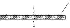
図2,3に示すように、検出チップ1は、透明基板2の表面上に閉鎖図形で描画される形状の閉鎖撥水部3が複数形成され、閉鎖撥水部3で囲まれた前記表面の部分が検出面とされる。
閉鎖撥水部3としては、前記閉鎖図形が正六角形状とされ、正六角形を構成する全ての辺において隣接する2つの閉鎖撥水部3同士が前記正六角形の一辺を共有するように形成される。
したがって、検出チップ1では、限られた領域に複数の閉鎖撥水部3を密に並べて配することで、多くの閉鎖撥水部3が形成される。
また、閉鎖撥水部3の前記閉鎖図形における最大径lとしては、小さい程、限られた領域に多数の閉鎖撥水部3を形成することができ、大きくとも5mmであることが好ましい。As shown in FIGS. The part of is the detection surface.
As the closed
Therefore, in the
Further, the maximum diameter l of the closed water-
次に、検出チップ1に液体試料を導入した様子を図4に示す。
検出チップ1の閉鎖撥水部3内に液体試料4を滴下して導入すると、図4に示すように、閉鎖撥水部3の撥水性により液体試料4が閉鎖撥水部3内、つまり、前記検出面上に保持される。
したがって、検出チップ1は、複数の閉鎖撥水部3により種類の異なる液体試料4を同時に保持し、それぞれの液体試料4を独立して観察可能なマルチチャンネル型の検出チップとされる。Next, FIG. 4 shows a state in which the liquid sample is introduced into the
When the
Therefore, the
再び図1を参照し、光照射部11は、透明基板2の裏面側から全反射条件で光を照射可能に構成される。
また、光検出部13は、検出チップ1(透明基板2)の前記表面側に配され、光Lの照射に基づき閉鎖撥水部3内に保持される液体試料に含まれる目的物質又は前記目的物質に結合した標識物質から発せられる蛍光又は散乱光を検出可能とされ、撮像デバイス等で構成される。With reference to FIG. 1 again, the
Further, the
目的物質検出装置10では、先ず、目的物質の検証を行う液体試料を閉鎖撥水部3に導入する。この際、複数の閉鎖撥水部3に対して、種類の異なる前記液体試料を導入し、保持させることで、マルチチャンネル化された前記目的物質の検出を行うことができる。
次に、光照射部11から複数の閉鎖撥水部3における前記検出面に向けて全反射条件で光Lを照射し、検出チップ1の前記表面近傍に前記エバネッセント場を形成させる。
次に、前記エバネッセント場を構成する前記エバネッセント光を励起光として、前記目的物質又は前記目的物質に結合して標識化する蛍光物質や光散乱物質などの標識物質から発せされる光の光信号Sを光検出部13で検出して、前記目的物質を検出する。In the target
Next, the light L is irradiated from the
Next, using the evanescent light constituting the evanescent field as excitation light, the optical signal S of light emitted from the target substance or a labeling substance such as a fluorescent substance or a light scattering substance that binds to and labels the target substance. Is detected by the
このように構成される目的物質検出装置10では、マルチチャンネル化にあたり、液体試料を個々の検出チップに送液する流路などの構造を作製する必要がなく、前記構造を作製する場合に比べ、より小型で低コストに製造することができる。 In the target
次に、本発明の前記目的物質検出装置及び前記目的物質検出方法の第2実施形態について図5を参照しつつ説明する。なお、図5は、第2実施形態の概略構成を示す説明図である。 Next, the second embodiment of the target substance detection device and the target substance detection method of the present invention will be described with reference to FIG. Note that FIG. 5 is an explanatory diagram showing a schematic configuration of the second embodiment.
図5に示すように目的物質検出装置20は、検出チップ1(図2~4参照)と光照射部21と光学プリズム22と光検出部23と磁場印加部24とで構成される。
目的物質検出装置20では、磁場印加部24が配される点で目的物質検出装置10と異なり、光照射部21、光学プリズム22及び光検出部23は、目的物質検出装置10における光照射部11、光学プリズム12及び光検出部13と同様に構成することができる。以下では、磁場印加部24に着目した説明を行う。As shown in FIG. 5, the target
The target
磁場印加部24は、永久磁石等を保持したスライド部材で構成され、透明基板2の裏面側に配されるとともに透明基板2の前記表面の面内方向と平行な方向のベクトル成分を持つ方向(図中のX1及びX2)にスライド移動可能とされる。
閉鎖撥水部3に保持される前記液体試料は、前記目的物質と結合体を構成する前記磁性粒子が添加されて調製される。
このような磁場印加部24が配される目的物質検出装置20では、前記液体試料中を浮遊する前記結合体の重力沈降を待つことなく、磁場印加部24による磁場の印加によって前記結合体を透明基板2の前記表面に引き寄せることができ、短時間での測定が可能とされる。
また、磁場印加部24の前記スライド移動に伴う前記結合体の移動の様子を前記スライド移動の前後で比較観察することで、前記磁場印加前における光信号に含まれるノイズ信号を排除した観察を行うことができる。
即ち、前記結合体が前記スライド移動により移動するのに対し、透明基板2表面のキズ等を原因とする前記ノイズ信号は、前記スライド移動により移動しないことから、前記スライド移動に伴って移動する光信号に着目した検出を行うことで、前記ノイズ信号を排除することができる。The magnetic
The liquid sample held in the closed water-
In the target
Further, by comparatively observing the movement of the coupled body accompanying the slide movement of the magnetic
That is, while the coupled body moves due to the slide movement, the noise signal caused by scratches on the surface of the
1 検出チップ
2 透明基板
3 閉鎖撥水部
4 液体試料
10,20 目的物質検出装置
11,21 光照射部
12,22 光学プリズム
13,23 光検出部
24 磁場印加部
1
Claims (6)
Translated fromJapanese前記検出面に向けて前記透明基板の裏面側から全反射条件で光を照射可能とされる光照射部と、
前記透明基板の前記表面側に配され、前記光の照射に基づき前記検出面上に保持される液体試料に含まれる目的物質又は前記目的物質に結合した標識物質から発せられる蛍光又は散乱光を検出可能とされる光検出部と、
が配されるとともに、前記検出面上に樹脂材料及びガラス材料のいずれかで形成される透明コーティング層が形成されることを特徴とする目的物質検出装置。A detection chip in which a plurality of closed water-repellent portionsdrawn inthe shape of a closed figure are formed on the surface of a transparent substrateby a linear film, and the surface portion surrounded by the closed water-repellent portions is used as a detection surface.
A light irradiation unit capable of irradiating light from the back surface side of the transparent substrate toward the detection surface under total reflection conditions.
Fluorescence or scattered light emitted from a target substance contained in a liquid sample arranged on the surface side of the transparent substrate and held on the detection surface based on the irradiation of the light or a labeling substance bound to the target substance is detected. Possible light detectors and
A target substance detection device, characterizedin that a transparent coating layer formed of either a resin material or a glass material is formed on the detection surface.
透明基板の検出面上に液体試料を導入する液体試料導入工程と、
前記検出面に向けて前記透明基板の裏面側から全反射条件で光を照射する光照射工程と、
前記光の照射に基づき前記液体試料に含まれる目的物質又は前記目的物質に結合した標識物質から発せられる蛍光又は散乱光を検出する光検出工程と、
を含むことを特徴とする目的物質検出方法。A target substance detection method for detecting a target substance using the target substance detection device according to any one of claims 1 to 5.
The liquid sample introduction process of introducing the liquid sample on the detection surface of the transparent substrate,
A light irradiation step of irradiating light from the back surface side of the transparent substrate toward the detection surface under total reflection conditions.
A light detection step of detecting fluorescence or scattered light emitted from a target substance contained in the liquid sample or a labeling substance bound to the target substance based on the irradiation of the light, and a light detection step.
A method for detecting a target substance, which comprises.
Priority Applications (1)
| Application Number | Priority Date | Filing Date | Title |
|---|---|---|---|
| JP2017136825AJP6991504B2 (en) | 2017-07-13 | 2017-07-13 | Target substance detection device and target substance detection method |
Applications Claiming Priority (1)
| Application Number | Priority Date | Filing Date | Title |
|---|---|---|---|
| JP2017136825AJP6991504B2 (en) | 2017-07-13 | 2017-07-13 | Target substance detection device and target substance detection method |
Publications (2)
| Publication Number | Publication Date |
|---|---|
| JP2019020180A JP2019020180A (en) | 2019-02-07 |
| JP6991504B2true JP6991504B2 (en) | 2022-01-12 |
Family
ID=65355438
Family Applications (1)
| Application Number | Title | Priority Date | Filing Date |
|---|---|---|---|
| JP2017136825AExpired - Fee RelatedJP6991504B2 (en) | 2017-07-13 | 2017-07-13 | Target substance detection device and target substance detection method |
Country Status (1)
| Country | Link |
|---|---|
| JP (1) | JP6991504B2 (en) |
Citations (9)
| Publication number | Priority date | Publication date | Assignee | Title |
|---|---|---|---|---|
| JP2002236258A (en) | 2001-01-25 | 2002-08-23 | Olympus Optical Co Ltd | Total reflection fluorescent microscope having white light source |
| JP2007033090A (en) | 2005-07-22 | 2007-02-08 | Asahi Glass Co Ltd | Optical detection substrate and manufacturing method thereof |
| JP2008275333A (en) | 2007-04-25 | 2008-11-13 | Canon Inc | Gene detection chip, nucleic acid sequence integration method and gene detection apparatus using the same |
| JP2009186459A (en) | 2008-01-10 | 2009-08-20 | Becton Dickinson & Co | Fast particle detection analysis |
| WO2010010751A1 (en) | 2008-07-25 | 2010-01-28 | 株式会社 日立ハイテクノロジーズ | Total reflection fluorescence observation device |
| JP2013238541A (en) | 2012-05-16 | 2013-11-28 | Toshiba Corp | Optical waveguide type measurement system and measurement method for glycosylated hemoglobin |
| JP2015524561A (en) | 2012-07-16 | 2015-08-24 | テクニシュ ユニベルシテイト デルフトTechnische Universiteit Delft | Single molecule protein sequencing |
| JP2016174608A (en) | 2005-06-15 | 2016-10-06 | カリダ・ジェノミックス・インコーポレイテッドCallida Genomics, Inc. | Single molecule arrays for genetic and chemical analysis |
| WO2016159324A1 (en) | 2015-03-31 | 2016-10-06 | 東レ株式会社 | Analysis chip |
Family Cites Families (2)
| Publication number | Priority date | Publication date | Assignee | Title |
|---|---|---|---|---|
| JPH07111430B2 (en)* | 1987-10-22 | 1995-11-29 | 日本電信電話株式会社 | Laser magnetic immunoassay method and measuring apparatus |
| GB9811480D0 (en)* | 1998-05-29 | 1998-07-29 | Photonic Research Systems Limi | Evanescent-wave excitation of upconverting labels |
- 2017
- 2017-07-13JPJP2017136825Apatent/JP6991504B2/ennot_activeExpired - Fee Related
Patent Citations (9)
| Publication number | Priority date | Publication date | Assignee | Title |
|---|---|---|---|---|
| JP2002236258A (en) | 2001-01-25 | 2002-08-23 | Olympus Optical Co Ltd | Total reflection fluorescent microscope having white light source |
| JP2016174608A (en) | 2005-06-15 | 2016-10-06 | カリダ・ジェノミックス・インコーポレイテッドCallida Genomics, Inc. | Single molecule arrays for genetic and chemical analysis |
| JP2007033090A (en) | 2005-07-22 | 2007-02-08 | Asahi Glass Co Ltd | Optical detection substrate and manufacturing method thereof |
| JP2008275333A (en) | 2007-04-25 | 2008-11-13 | Canon Inc | Gene detection chip, nucleic acid sequence integration method and gene detection apparatus using the same |
| JP2009186459A (en) | 2008-01-10 | 2009-08-20 | Becton Dickinson & Co | Fast particle detection analysis |
| WO2010010751A1 (en) | 2008-07-25 | 2010-01-28 | 株式会社 日立ハイテクノロジーズ | Total reflection fluorescence observation device |
| JP2013238541A (en) | 2012-05-16 | 2013-11-28 | Toshiba Corp | Optical waveguide type measurement system and measurement method for glycosylated hemoglobin |
| JP2015524561A (en) | 2012-07-16 | 2015-08-24 | テクニシュ ユニベルシテイト デルフトTechnische Universiteit Delft | Single molecule protein sequencing |
| WO2016159324A1 (en) | 2015-03-31 | 2016-10-06 | 東レ株式会社 | Analysis chip |
Non-Patent Citations (1)
| Title |
|---|
| GENTILE, F. et al.,Selective on site separation and detection of molecules in diluted solution with super-hydrophobic clusters of plasmonic nanoparticles,Nanoscale,2014年05月12日,Vol. 6,pp. 8208-8225,doi: 10.1039/C4NR00796D |
Also Published As
| Publication number | Publication date |
|---|---|
| JP2019020180A (en) | 2019-02-07 |
Similar Documents
| Publication | Publication Date | Title |
|---|---|---|
| JP7008334B2 (en) | Optical detection method and optical detection device | |
| EP1912740B1 (en) | Optical assay system | |
| JP2019168471A (en) | Detecting and using of light representing sample | |
| US11112359B2 (en) | Target substance detection chip, target substance detection device, and target substance detection method | |
| US20110027916A1 (en) | Detection apparatus for detecting particles | |
| JP6225114B2 (en) | Cluster detection device | |
| JP2014081385A (en) | Microplate having periodic structure, surface plasmon excitation enhanced fluorescence microscope or fluorescence microplate reader using the same, and detection method | |
| Agnarsson et al. | Fabrication of planar polymer waveguides for evanescent-wave sensing in aqueous environments | |
| JP6738070B2 (en) | Optical detection device and optical detection method | |
| WO2018100780A1 (en) | Target substance detection device and target substance detection method | |
| JP6991504B2 (en) | Target substance detection device and target substance detection method | |
| CN111788473A (en) | Device for detecting binding affinity | |
| JP2016118389A (en) | Interaction analyzer | |
| JP5923811B2 (en) | Target substance detection plate, target substance detection apparatus, and target substance detection method | |
| EP2380022B1 (en) | Sensing device for detecting target elements in a fluid | |
| CN105572046B (en) | Fluoroscopic examination sample cell and preparation method thereof | |
| JP5891990B2 (en) | Optical specimen detector | |
| JP6936987B2 (en) | Target substance detection chip, target substance detection device and target substance detection method | |
| JP7029121B2 (en) | Target substance detection chip, target substance detection device and target substance detection method | |
| JP7411219B2 (en) | Target substance detection device and target substance detection method using magnetic field and gravity | |
| JP6928930B2 (en) | Target substance detection chip, target substance detection device and target substance detection method | |
| JP2008051512A (en) | Sensor using near-field light and manufacturing method thereof | |
| JP6482774B2 (en) | Biological analysis device, analysis apparatus, and analysis method | |
| JP7097563B2 (en) | Target substance detection device and target substance detection method | |
| HK40037086A (en) | Device for use in the detection of binding affinities |
Legal Events
| Date | Code | Title | Description |
|---|---|---|---|
| A621 | Written request for application examination | Free format text:JAPANESE INTERMEDIATE CODE: A621 Effective date:20200603 | |
| A977 | Report on retrieval | Free format text:JAPANESE INTERMEDIATE CODE: A971007 Effective date:20210215 | |
| A131 | Notification of reasons for refusal | Free format text:JAPANESE INTERMEDIATE CODE: A131 Effective date:20210330 | |
| A521 | Request for written amendment filed | Free format text:JAPANESE INTERMEDIATE CODE: A523 Effective date:20210520 | |
| TRDD | Decision of grant or rejection written | ||
| A01 | Written decision to grant a patent or to grant a registration (utility model) | Free format text:JAPANESE INTERMEDIATE CODE: A01 Effective date:20211109 | |
| A61 | First payment of annual fees (during grant procedure) | Free format text:JAPANESE INTERMEDIATE CODE: A61 Effective date:20211129 | |
| R150 | Certificate of patent or registration of utility model | Ref document number:6991504 Country of ref document:JP Free format text:JAPANESE INTERMEDIATE CODE: R150 | |
| S533 | Written request for registration of change of name | Free format text:JAPANESE INTERMEDIATE CODE: R313533 | |
| R350 | Written notification of registration of transfer | Free format text:JAPANESE INTERMEDIATE CODE: R350 | |
| LAPS | Cancellation because of no payment of annual fees |