JP6987107B2 - Semiconductor device - Google Patents
Semiconductor deviceDownload PDFInfo
- Publication number
- JP6987107B2 JP6987107B2JP2019205138AJP2019205138AJP6987107B2JP 6987107 B2JP6987107 B2JP 6987107B2JP 2019205138 AJP2019205138 AJP 2019205138AJP 2019205138 AJP2019205138 AJP 2019205138AJP 6987107 B2JP6987107 B2JP 6987107B2
- Authority
- JP
- Japan
- Prior art keywords
- film
- oxide semiconductor
- insulating film
- transistor
- semiconductor film
- Prior art date
- Legal status (The legal status is an assumption and is not a legal conclusion. Google has not performed a legal analysis and makes no representation as to the accuracy of the status listed.)
- Active
Links
Images


Classifications
- H—ELECTRICITY
- H10—SEMICONDUCTOR DEVICES; ELECTRIC SOLID-STATE DEVICES NOT OTHERWISE PROVIDED FOR
- H10D—INORGANIC ELECTRIC SEMICONDUCTOR DEVICES
- H10D30/00—Field-effect transistors [FET]
- H10D30/60—Insulated-gate field-effect transistors [IGFET]
- H10D30/67—Thin-film transistors [TFT]
- H10D30/674—Thin-film transistors [TFT] characterised by the active materials
- H10D30/6755—Oxide semiconductors, e.g. zinc oxide, copper aluminium oxide or cadmium stannate
- H—ELECTRICITY
- H10—SEMICONDUCTOR DEVICES; ELECTRIC SOLID-STATE DEVICES NOT OTHERWISE PROVIDED FOR
- H10D—INORGANIC ELECTRIC SEMICONDUCTOR DEVICES
- H10D30/00—Field-effect transistors [FET]
- H10D30/60—Insulated-gate field-effect transistors [IGFET]
- H10D30/67—Thin-film transistors [TFT]
- H10D30/6704—Thin-film transistors [TFT] having supplementary regions or layers in the thin films or in the insulated bulk substrates for controlling properties of the device
- H—ELECTRICITY
- H10—SEMICONDUCTOR DEVICES; ELECTRIC SOLID-STATE DEVICES NOT OTHERWISE PROVIDED FOR
- H10D—INORGANIC ELECTRIC SEMICONDUCTOR DEVICES
- H10D30/00—Field-effect transistors [FET]
- H10D30/60—Insulated-gate field-effect transistors [IGFET]
- H10D30/67—Thin-film transistors [TFT]
- H10D30/6729—Thin-film transistors [TFT] characterised by the electrodes
- H10D30/673—Thin-film transistors [TFT] characterised by the electrodes characterised by the shapes, relative sizes or dispositions of the gate electrodes
- H10D30/6733—Multi-gate TFTs
- H10D30/6734—Multi-gate TFTs having gate electrodes arranged on both top and bottom sides of the channel, e.g. dual-gate TFTs
- H—ELECTRICITY
- H10—SEMICONDUCTOR DEVICES; ELECTRIC SOLID-STATE DEVICES NOT OTHERWISE PROVIDED FOR
- H10D—INORGANIC ELECTRIC SEMICONDUCTOR DEVICES
- H10D30/00—Field-effect transistors [FET]
- H10D30/60—Insulated-gate field-effect transistors [IGFET]
- H10D30/67—Thin-film transistors [TFT]
- H10D30/6729—Thin-film transistors [TFT] characterised by the electrodes
- H10D30/6737—Thin-film transistors [TFT] characterised by the electrodes characterised by the electrode materials
- H10D30/6739—Conductor-insulator-semiconductor electrodes
- H—ELECTRICITY
- H10—SEMICONDUCTOR DEVICES; ELECTRIC SOLID-STATE DEVICES NOT OTHERWISE PROVIDED FOR
- H10D—INORGANIC ELECTRIC SEMICONDUCTOR DEVICES
- H10D30/00—Field-effect transistors [FET]
- H10D30/60—Insulated-gate field-effect transistors [IGFET]
- H10D30/67—Thin-film transistors [TFT]
- H10D30/6757—Thin-film transistors [TFT] characterised by the structure of the channel, e.g. transverse or longitudinal shape or doping profile
- H—ELECTRICITY
- H10—SEMICONDUCTOR DEVICES; ELECTRIC SOLID-STATE DEVICES NOT OTHERWISE PROVIDED FOR
- H10D—INORGANIC ELECTRIC SEMICONDUCTOR DEVICES
- H10D62/00—Semiconductor bodies, or regions thereof, of devices having potential barriers
- H10D62/10—Shapes, relative sizes or dispositions of the regions of the semiconductor bodies; Shapes of the semiconductor bodies
- H10D62/102—Constructional design considerations for preventing surface leakage or controlling electric field concentration
- H—ELECTRICITY
- H10—SEMICONDUCTOR DEVICES; ELECTRIC SOLID-STATE DEVICES NOT OTHERWISE PROVIDED FOR
- H10D—INORGANIC ELECTRIC SEMICONDUCTOR DEVICES
- H10D62/00—Semiconductor bodies, or regions thereof, of devices having potential barriers
- H10D62/80—Semiconductor bodies, or regions thereof, of devices having potential barriers characterised by the materials
- H10D62/81—Semiconductor bodies, or regions thereof, of devices having potential barriers characterised by the materials of structures exhibiting quantum-confinement effects, e.g. single quantum wells; of structures having periodic or quasi-periodic potential variation
- H—ELECTRICITY
- H10—SEMICONDUCTOR DEVICES; ELECTRIC SOLID-STATE DEVICES NOT OTHERWISE PROVIDED FOR
- H10D—INORGANIC ELECTRIC SEMICONDUCTOR DEVICES
- H10D64/00—Electrodes of devices having potential barriers
- H10D64/60—Electrodes characterised by their materials
- H10D64/66—Electrodes having a conductor capacitively coupled to a semiconductor by an insulator, e.g. MIS electrodes
- H10D64/68—Electrodes having a conductor capacitively coupled to a semiconductor by an insulator, e.g. MIS electrodes characterised by the insulator, e.g. by the gate insulator
- H10D64/691—Electrodes having a conductor capacitively coupled to a semiconductor by an insulator, e.g. MIS electrodes characterised by the insulator, e.g. by the gate insulator comprising metallic compounds, e.g. metal oxides or metal silicates
- H—ELECTRICITY
- H10—SEMICONDUCTOR DEVICES; ELECTRIC SOLID-STATE DEVICES NOT OTHERWISE PROVIDED FOR
- H10D—INORGANIC ELECTRIC SEMICONDUCTOR DEVICES
- H10D86/00—Integrated devices formed in or on insulating or conducting substrates, e.g. formed in silicon-on-insulator [SOI] substrates or on stainless steel or glass substrates
- H10D86/40—Integrated devices formed in or on insulating or conducting substrates, e.g. formed in silicon-on-insulator [SOI] substrates or on stainless steel or glass substrates characterised by multiple TFTs
- H10D86/421—Integrated devices formed in or on insulating or conducting substrates, e.g. formed in silicon-on-insulator [SOI] substrates or on stainless steel or glass substrates characterised by multiple TFTs having a particular composition, shape or crystalline structure of the active layer
- H10D86/423—Integrated devices formed in or on insulating or conducting substrates, e.g. formed in silicon-on-insulator [SOI] substrates or on stainless steel or glass substrates characterised by multiple TFTs having a particular composition, shape or crystalline structure of the active layer comprising semiconductor materials not belonging to the Group IV, e.g. InGaZnO
- H—ELECTRICITY
- H10—SEMICONDUCTOR DEVICES; ELECTRIC SOLID-STATE DEVICES NOT OTHERWISE PROVIDED FOR
- H10D—INORGANIC ELECTRIC SEMICONDUCTOR DEVICES
- H10D86/00—Integrated devices formed in or on insulating or conducting substrates, e.g. formed in silicon-on-insulator [SOI] substrates or on stainless steel or glass substrates
- H10D86/40—Integrated devices formed in or on insulating or conducting substrates, e.g. formed in silicon-on-insulator [SOI] substrates or on stainless steel or glass substrates characterised by multiple TFTs
- H10D86/481—Integrated devices formed in or on insulating or conducting substrates, e.g. formed in silicon-on-insulator [SOI] substrates or on stainless steel or glass substrates characterised by multiple TFTs integrated with passive devices, e.g. auxiliary capacitors
- H—ELECTRICITY
- H10—SEMICONDUCTOR DEVICES; ELECTRIC SOLID-STATE DEVICES NOT OTHERWISE PROVIDED FOR
- H10D—INORGANIC ELECTRIC SEMICONDUCTOR DEVICES
- H10D86/00—Integrated devices formed in or on insulating or conducting substrates, e.g. formed in silicon-on-insulator [SOI] substrates or on stainless steel or glass substrates
- H10D86/40—Integrated devices formed in or on insulating or conducting substrates, e.g. formed in silicon-on-insulator [SOI] substrates or on stainless steel or glass substrates characterised by multiple TFTs
- H10D86/60—Integrated devices formed in or on insulating or conducting substrates, e.g. formed in silicon-on-insulator [SOI] substrates or on stainless steel or glass substrates characterised by multiple TFTs wherein the TFTs are in active matrices
- H—ELECTRICITY
- H10—SEMICONDUCTOR DEVICES; ELECTRIC SOLID-STATE DEVICES NOT OTHERWISE PROVIDED FOR
- H10D—INORGANIC ELECTRIC SEMICONDUCTOR DEVICES
- H10D99/00—Subject matter not provided for in other groups of this subclass
- H—ELECTRICITY
- H10—SEMICONDUCTOR DEVICES; ELECTRIC SOLID-STATE DEVICES NOT OTHERWISE PROVIDED FOR
- H10D—INORGANIC ELECTRIC SEMICONDUCTOR DEVICES
- H10D30/00—Field-effect transistors [FET]
- H10D30/60—Insulated-gate field-effect transistors [IGFET]
- H10D30/62—Fin field-effect transistors [FinFET]
Landscapes
- Thin Film Transistor (AREA)
- Semiconductor Memories (AREA)
- Metal-Oxide And Bipolar Metal-Oxide Semiconductor Integrated Circuits (AREA)
- Physical Vapour Deposition (AREA)
- Chemical Vapour Deposition (AREA)
- Formation Of Insulating Films (AREA)
Description
Translated fromJapanese 本発明は、物、方法、または製造方法に関する。または、本発明は、プロセス、マシン
、マニュファクチャ、または組成物(コンポジション・オブ・マター)に関する。また、
本発明の一態様は、半導体装置、表示装置、発光装置、蓄電装置、記憶装置、それらの駆
動方法またはそれらの製造方法に関する。特に、本発明の一態様は、半導体装置、または
半導体装置の製造方法に関する。The present invention relates to a product, a method, or a manufacturing method. Alternatively, the invention relates to a process, machine, manufacture, or composition (composition of matter). also,
One aspect of the present invention relates to a semiconductor device, a display device, a light emitting device, a power storage device, a storage device, a method for driving the same, or a method for manufacturing the same. In particular, one aspect of the present invention relates to a semiconductor device or a method for manufacturing a semiconductor device.
なお、本明細書中において半導体装置とは、半導体特性を利用することで機能しうる装
置全般を指す。表示装置、電気光学装置、半導体回路および電気機器は、半導体装置を有
している場合がある。In the present specification, the semiconductor device refers to all devices that can function by utilizing the semiconductor characteristics. Display devices, electro-optic devices, semiconductor circuits and electrical devices may include semiconductor devices.
半導体膜を用いてトランジスタを構成する技術が注目されている。当該トランジスタは
集積回路(IC)や画像表示装置(表示装置)のような電子デバイスに広く応用されてい
る。トランジスタに適用可能な半導体薄膜の材料としてシリコン系半導体材料が広く知ら
れているが、その他の材料として酸化物半導体が注目されている。Attention is being paid to a technique for constructing a transistor using a semiconductor film. The transistor is widely applied to electronic devices such as integrated circuits (ICs) and image display devices (display devices). Silicon-based semiconductor materials are widely known as materials for semiconductor thin films applicable to transistors, but oxide semiconductors are attracting attention as other materials.
例えば、インジウム(In)、ガリウム(Ga)、および亜鉛(Zn)を含む非晶質酸
化物半導体膜を用いたトランジスタが特許文献1に開示されている。For example,
また、酸化物半導体膜を、積層構造とすることで、キャリアの移動度を向上させる技術
が特許文献2、特許文献3に開示されている。Further,
ところで、酸化物半導体膜を用いたトランジスタは、オフ状態において極めてリーク電
流(オフ電流)が小さいことが知られている。例えば、酸化物半導体膜を用いたトランジ
スタの低いリーク特性を応用した低消費電力のCPUなどが開示されている(特許文献4
参照。)。By the way, it is known that a transistor using an oxide semiconductor film has an extremely small leakage current (off current) in an off state. For example, a low power consumption CPU that applies the low leakage characteristics of a transistor using an oxide semiconductor film is disclosed (Patent Document 4).
reference. ).
オフ電流を小さくするためには、酸化物半導体の性質だけでなく、他の構成のリーク源
についても細心の注意を払う必要がある。In order to reduce the off-current, it is necessary to pay close attention not only to the properties of oxide semiconductors but also to the leak sources of other configurations.
たとえば、ゲート絶縁膜を薄くしていくとゲート絶縁膜に起因したリーク電流が増大す
る。また、Fin型のような立体的な構造を有する電界効果トランジスタ(FET)にお
いては、段差被覆性の低下によるゲート絶縁膜起因のリーク電流が発生しやすい。一方で
、特に微細化されたトランジスタにおいては、ゲート絶縁膜の薄膜化は重要である。For example, as the gate insulating film is made thinner, the leakage current caused by the gate insulating film increases. Further, in a field effect transistor (FET) having a three-dimensional structure such as a Fin type, a leakage current due to a gate insulating film due to a decrease in step covering property is likely to occur. On the other hand, it is important to reduce the thickness of the gate insulating film, especially for miniaturized transistors.
そこで、ゲート絶縁膜に起因したリーク電流を低減することができるゲート絶縁膜を提
供する。具体的には酸化ハフニウムなどの高誘電率(High−k)絶縁膜を用いること
で等価酸化膜厚(EOT:Equivalent Oxide Thickness)を
厚くする。なお、等価酸化膜厚とは、物理的な膜厚を酸化シリコンと等価な電気的膜厚に
換算した値をいう。Therefore, a gate insulating film capable of reducing the leakage current caused by the gate insulating film is provided. Specifically, the equivalent oxide film thickness (EOT: Equivalent Oxide Tickness) is increased by using a high dielectric constant (High-k) insulating film such as hafnium oxide. The equivalent oxide film thickness is a value obtained by converting the physical film thickness into an electrical film thickness equivalent to silicon oxide.
また、本発明の一態様は、オン電流が高く、オフ電流が低い半導体装置を提供すること
を課題の一とする。または、安定な電気特性をもつ半導体装置を提供することを課題の一
とする。または、新規な半導体装置を提供することを課題の一とする。Further, one aspect of the present invention is to provide a semiconductor device having a high on-current and a low off-current. Another issue is to provide a semiconductor device having stable electrical characteristics. Alternatively, one of the issues is to provide a new semiconductor device.
なお、これらの課題の記載は、他の課題の存在を妨げるものではない。なお、本発明の
一態様は、これらの課題の全てを解決する必要はないものとする。なお、これら以外の課
題は、明細書、図面、請求項などの記載から、自ずと明らかとなるものであり、明細書、
図面、請求項などの記載から、これら以外の課題を抽出することが可能である。The description of these issues does not preclude the existence of other issues. It should be noted that one aspect of the present invention does not need to solve all of these problems. Issues other than these are self-evident from the description of the description, drawings, claims, etc.
It is possible to extract problems other than these from the drawings, claims, and the like.
本発明の一態様は、絶縁表面上の第1の酸化物半導体膜と、第1の酸化物半導体膜上の
第2の酸化物半導体膜と、第1の酸化物半導体膜の側面、第2の酸化物半導体膜の側面お
よび第2の酸化物半導体膜の上面と接するソース電極およびドレイン電極と、第2の酸化
物半導体膜上の第3の酸化物半導体膜と、第3の酸化物半導体膜上の第1のゲート絶縁膜
と、第1のゲート絶縁膜上の第2のゲート絶縁膜と、第2のゲート絶縁膜上で接し、第2
の酸化物半導体膜の上面および側面に面するゲート電極と、を有し、第1のゲート絶縁膜
は、ハフニウムを含み、第2のゲート絶縁膜は、シリコンを含むことを特徴とする半導体
装置である。One aspect of the present invention is a first oxide semiconductor film on an insulating surface, a second oxide semiconductor film on a first oxide semiconductor film, a side surface of the first oxide semiconductor film, and a second. A source electrode and a drain electrode in contact with the side surface of the oxide semiconductor film and the upper surface of the second oxide semiconductor film, a third oxide semiconductor film on the second oxide semiconductor film, and a third oxide semiconductor. The first gate insulating film on the film, the second gate insulating film on the first gate insulating film, and the second gate insulating film on the second gate insulating film are in contact with each other.
A semiconductor device comprising: gate electrodes facing the upper surface and side surfaces of the oxide semiconductor film of the above, wherein the first gate insulating film contains hafnium and the second gate insulating film contains silicon. Is.
また、本発明の他の一態様は、絶縁表面上の第1の酸化物半導体膜と、第1の酸化物半
導体膜上の第2の酸化物半導体膜と、第2の酸化物半導体膜上の第3の酸化物半導体膜と
、第3の酸化物半導体膜上の第1のゲート絶縁膜と、第1の酸化物半導体膜、第2の酸化
物半導体膜、第3の酸化物半導体膜および第1のゲート絶縁膜の側面、第1のゲート絶縁
膜の上面と接するソース電極およびドレイン電極と、第1のゲート絶縁膜、ソース電極お
よびドレイン電極上の第2のゲート絶縁膜と、第2のゲート絶縁膜上で接し、第2の酸化
物半導体膜の上面および側面に面するゲート電極と、を有し、第1のゲート絶縁膜は、ハ
フニウムを含み、第2のゲート絶縁膜は、シリコンを含むことを特徴とする半導体装置で
ある。Further, another aspect of the present invention is on the first oxide semiconductor film on the insulating surface, the second oxide semiconductor film on the first oxide semiconductor film, and the second oxide semiconductor film. The third oxide semiconductor film, the first gate insulating film on the third oxide semiconductor film, the first oxide semiconductor film, the second oxide semiconductor film, and the third oxide semiconductor film. And a source electrode and a drain electrode in contact with the side surface of the first gate insulating film and the upper surface of the first gate insulating film, a second gate insulating film on the first gate insulating film, the source electrode and the drain electrode, and a second gate insulating film. It has a gate electrode that is in contact with the gate insulating film of 2 and faces the upper surface and the side surface of the second oxide semiconductor film, the first gate insulating film contains hafnium, and the second gate insulating film contains hafnium. , A semiconductor device characterized by containing silicon.
また、上記構成において、第1の酸化物半導体膜および第3の酸化物半導体膜は、第2
の酸化物半導体膜に含まれる金属元素を一種以上含む。Further, in the above configuration, the first oxide semiconductor film and the third oxide semiconductor film are the second oxide semiconductor film.
Contains one or more metal elements contained in the oxide semiconductor film of.
また、上記構成において、第1のゲート絶縁膜は、X線回折によって測定した回折角2
θ=28°近傍にピークが観測される。Further, in the above configuration, the first gate insulating film has a
A peak is observed near θ = 28 °.
また、上記構成において、第2の酸化物半導体膜のバンドギャップは、第1のゲート絶
縁膜のバンドギャップよりも小さく、第1のゲート絶縁膜のバンドギャップは、第2のゲ
ート絶縁膜のバンドギャップよりも小さい。Further, in the above configuration, the band gap of the second oxide semiconductor film is smaller than the band gap of the first gate insulating film, and the band gap of the first gate insulating film is the band of the second gate insulating film. Smaller than the gap.
また、本発明の他の一態様は、第1の酸化物半導体膜と、第1の酸化物半導体膜と重な
るゲート電極と、第1の酸化物半導体膜およびゲート電極の間に位置する第1のゲート絶
縁膜と、第1のゲート絶縁膜およびゲート電極との間に位置する第2のゲート絶縁膜と、
を有し、第1のゲート絶縁膜は、X線回折によって測定した回折角2θ=28°近傍にピ
ークが観測されることを特徴とする半導体装置である。Further, another aspect of the present invention is a first aspect located between the first oxide semiconductor film, the gate electrode overlapping the first oxide semiconductor film, and the first oxide semiconductor film and the gate electrode. A second gate insulating film located between the gate insulating film and the first gate insulating film and the gate electrode.
The first gate insulating film is a semiconductor device characterized in that a peak is observed in the vicinity of a diffraction angle of 2θ = 28 ° measured by X-ray diffraction.
また、上記構成において、第1のゲート絶縁膜は、ハフニウムを含む。 Further, in the above configuration, the first gate insulating film contains hafnium.
また、上記構成において、第2のゲート絶縁膜は、シリコンを含む。 Further, in the above configuration, the second gate insulating film contains silicon.
また、上記構成において、第1の酸化物半導体膜は、第2の酸化物半導体膜と、第1の
酸化物半導体膜と第1のゲート絶縁膜との間に位置する第3の酸化物半導体膜と、に挟持
され、第2の酸化物半導体膜および第3の酸化物半導体膜は、第1の酸化物半導体膜に含
まれる金属元素を一種以上含む。Further, in the above configuration, the first oxide semiconductor film is a third oxide semiconductor located between the second oxide semiconductor film, the first oxide semiconductor film, and the first gate insulating film. The second oxide semiconductor film and the third oxide semiconductor film sandwiched between the film and the film contain one or more metal elements contained in the first oxide semiconductor film.
また、上記構成において、第1の酸化物半導体膜のバンドギャップは、第1のゲート絶
縁膜のバンドギャップよりも小さく、第1のゲート絶縁膜のバンドギャップは、第2のゲ
ート絶縁膜のバンドギャップよりも小さい。Further, in the above configuration, the band gap of the first oxide semiconductor film is smaller than the band gap of the first gate insulating film, and the band gap of the first gate insulating film is the band of the second gate insulating film. Smaller than the gap.
また、上記構成において、第1のゲート絶縁膜の膜密度は、8.3g/cm3以上9.
0g/cm3以下であると好ましい。Further, in the above configuration, the film density of the first gate insulating film is 8.3 g / cm3 or more 9.
It is preferably 0 g / cm3 or less.
また、上記構成において、第1のゲート絶縁膜は、電子スピン共鳴法によって計測され
る信号において、g値が1.92乃至1.98に現れるスピン密度が3.0×10¹⁷s
pins/cm3以下であり、g値が2.00乃至2.01に現れるスピン密度が4.4
×1016spins/cm3以上3.5×1018spins/cm3以下であると好
ましい。Further, in the above configuration, the first gate insulating film has a spin density of 3.0 × 10 17 s in which the g value appears at 1.92 to 1.98 in the signal measured by the electron spin resonance method.
The spin density is 4.4 when the g value is 2.00 to 2.01 and the pins / cm is3 or less.
It is preferably × 1016 spins / cm3 or more and 3.5 × 10¹⁸ spins / cm3 or less.
また、上記構成において、第1のゲート絶縁膜の電子スピン共鳴法によって計測される
信号において、g値が2.00乃至2.01に現れるシグナルの形状は非対称である。Further, in the above configuration, in the signal measured by the electron spin resonance method of the first gate insulating film, the shape of the signal whose g value appears in 2.00 to 2.01 is asymmetric.
本発明の一態様を用いることにより、オン電流が高く、オフ電流が低い半導体装置を提
供することができる。または、安定な電気特性をもつ半導体装置を提供することができる
。または、本発明の一態様を用いることにより、新規な半導体装置などを提供することが
できる。なお、これらの効果の記載は、他の効果の存在を妨げるものではない。なお、本
発明の一態様は、必ずしも、これらの効果の全てを有する必要はない。なお、これら以外
の効果は、明細書、図面、請求項などの記載から、自ずと明らかとなるものであり、明細
書、図面、請求項などの記載から、これら以外の効果を抽出することが可能である。By using one aspect of the present invention, it is possible to provide a semiconductor device having a high on-current and a low off-current. Alternatively, it is possible to provide a semiconductor device having stable electrical characteristics. Alternatively, by using one aspect of the present invention, a novel semiconductor device or the like can be provided. The description of these effects does not preclude the existence of other effects. It should be noted that one aspect of the present invention does not necessarily have to have all of these effects. It should be noted that the effects other than these are self-evident from the description of the description, drawings, claims, etc., and it is possible to extract the effects other than these from the description of the description, drawings, claims, etc. Is.
実施の形態について、図面を用いて詳細に説明する。但し、本発明は以下の説明に限定
されず、本発明の趣旨およびその範囲から逸脱することなくその形態および詳細を様々に
変更し得ることは当業者であれば容易に理解される。したがって、本発明は以下に示す実
施の形態の記載内容に限定して解釈されるものではない。なお、以下に説明する発明の構
成において、同一部分または同様な機能を有する部分には同一の符号を異なる図面間で共
通して用い、その繰り返しの説明は省略することがある。The embodiments will be described in detail with reference to the drawings. However, the present invention is not limited to the following description, and it is easily understood by those skilled in the art that the form and details thereof can be variously changed without departing from the spirit and scope of the present invention. Therefore, the present invention is not construed as being limited to the description of the embodiments shown below. In the configuration of the invention described below, the same reference numerals may be used in common among different drawings for the same parts or parts having similar functions, and the repeated description thereof may be omitted.
なお、トランジスタの「ソース」や「ドレイン」の機能は、異なる極性のトランジスタ
を採用する場合や、回路動作において電流の方向が変化する場合などには入れ替わること
がある。このため、本明細書においては、「ソース」や「ドレイン」という用語は、入れ
替えて用いることができるものとする。The "source" and "drain" functions of the transistor may be interchanged when a transistor having a different polarity is used or when the direction of the current changes in the circuit operation. Therefore, in the present specification, the terms "source" and "drain" may be used interchangeably.
なお、ある一つの実施の形態の中で述べる内容(一部の内容でもよい)は、その実施の
形態で述べる別の内容(一部の内容でもよい)、および/または、一つ若しくは複数の別
の実施の形態で述べる内容(一部の内容でもよい)に対して、適用、組み合わせ、または
置き換えなどを行うことができる。It should be noted that the content described in one embodiment (may be a part of the content) is another content (may be a part of the content) described in the embodiment, and / or one or more. It can be applied, combined, or replaced with respect to the content described in another embodiment (which may be a partial content).
なお、実施の形態の中で述べる内容とは、各々の実施の形態において、様々な図を用い
て述べる内容、または明細書に記載される文章を用いて述べる内容のことである。In addition, the content described in the embodiment is the content described by using various figures or the content described by using the text described in the specification in each embodiment.
なお、ある一つの実施の形態において述べる図(一部でもよい)は、その図の別の部分
、その実施の形態において述べる別の図(一部でもよい)、および/または、一つ若しく
は複数の別の実施の形態において述べる図(一部でもよい)に対して、組み合わせること
により、さらに多くの図を構成させることができる。It should be noted that the figure (which may be a part) described in one embodiment is another part of the figure, another figure (which may be a part) described in the embodiment, and / or one or more. By combining the figures (which may be a part) described in another embodiment of the above, more figures can be formed.
(実施の形態1)
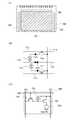
本実施の形態では、本発明の一態様の半導体装置に含まれる積層構造について図2を参
照して説明する。(Embodiment 1)
In the present embodiment, the laminated structure included in the semiconductor device of one aspect of the present invention will be described with reference to FIG.
本発明の一態様は、ゲート絶縁膜に起因したリーク電流を低減するためHigh−k絶
縁膜を用いることで等価酸化膜厚を厚くする。One aspect of the present invention is to increase the equivalent oxide film thickness by using a High-k insulating film in order to reduce the leakage current caused by the gate insulating film.
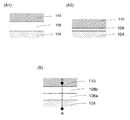
図2(A1)および図2(A2)に、本発明の一態様の半導体装置に含まれる積層構造
の概念図を示す。2 (A1) and 2 (A2) show conceptual diagrams of the laminated structure included in the semiconductor device of one aspect of the present invention.
図2(A1)および図2(A2)は酸化物半導体膜104と、酸化物半導体膜104上
のゲート絶縁膜108と、ゲート絶縁膜108を介して酸化物半導体膜104と重なるゲ
ート電極110を有する半導体装置である。2 (A1) and 2 (A2) show the
図2(A1)の半導体装置のゲート絶縁膜108にはHigh−k絶縁膜(ここでは酸
化ハフニウム:誘電率16)を用い、図2(A2)の半導体装置のゲート絶縁膜108に
は通常の絶縁膜(ここでは酸化シリコン:誘電率3.9)を用いている。A high-k insulating film (here, hafnium oxide: dielectric constant 16) is used for the
ゲート絶縁膜108に用いる材料を誘電率が大きいものにすると、ゲート絶縁膜108
を厚くすることができる。たとえば、誘電率が16の酸化ハフニウムを用いることにより
、誘電率が3.9の酸化シリコンを用いる場合に比べて約4倍厚くすることが可能である
。そのため、異物(ゴミなど)によるショートを防止することや、段差被覆性の低下を抑
制することができ好ましい。When the material used for the
Can be thickened. For example, by using hafnium oxide having a dielectric constant of 16, it is possible to make it about four times thicker than when silicon oxide having a dielectric constant of 3.9 is used. Therefore, it is preferable because it is possible to prevent a short circuit due to a foreign substance (dust or the like) and to suppress a decrease in the step covering property.
しかし、High−k絶縁膜は、物理的膜厚を厚くすることが可能であるものの、多結
晶化しやすく、結晶粒界に起因したリーク電流が流れる場合がある。また、ゲート電極と
の密着性が低下することもある。なお、High−k絶縁膜は非晶質状態では誘電率が低
く、物理的膜厚を厚くできる効果が小さい。また、非晶質状態で使用することで、成膜時
の温度や後のベーク温度を低くせざるを得ず、膜質が悪くなる場合がある。However, although the high-k insulating film can have a thick physical film thickness, it is easily polycrystallized and a leak current due to grain boundaries may flow. In addition, the adhesion to the gate electrode may decrease. The high-k insulating film has a low dielectric constant in an amorphous state, and the effect of increasing the physical film thickness is small. Further, when used in an amorphous state, the temperature at the time of film formation and the baking temperature after that must be lowered, and the film quality may deteriorate.
そのため、図2(B)に示すようにHigh−k絶縁膜であるゲート絶縁膜108aと
ゲート電極110との間に酸化シリコン膜や酸化窒化シリコン膜などで構成されたゲート
絶縁膜108bを形成することで、物理的膜厚を確保しつつ、結晶粒界に起因したリーク
電流も低減し、かつゲート電極との密着性を確保することができる。Therefore, as shown in FIG. 2B, a
また、酸化物半導体膜104と接するゲート絶縁膜108aは成膜時に酸化物半導体膜
104に酸素を供給する絶縁膜であると好ましい。なお、ゲート絶縁膜108aの成膜時
にゲート絶縁膜108aの下の膜(酸化物半導体膜104)に酸素を導入するには、成膜
時に酸素を含む雰囲気下で成膜を行えばよく、酸素割合が大きい方が酸素を多く導入する
ことができるため好ましい。また、ゲート絶縁膜108aは、酸素、水素、水等のブロッ
キング機能を有する絶縁膜であると好ましい。Further, the
上記のような機能を有する絶縁膜を設けることで、ゲート絶縁膜成膜時に酸化物半導体
膜に酸素を供給することができ、かつ酸化物半導体膜中の酸素の外部への拡散を防ぐこと
によって酸化物半導体膜中の酸素欠損を低減でき、また、外部から酸化物半導体膜への水
素、水等の混入を防ぐことができる。By providing the insulating film having the above-mentioned functions, oxygen can be supplied to the oxide semiconductor film at the time of forming the gate insulating film, and oxygen in the oxide semiconductor film can be prevented from diffusing to the outside. Oxygen deficiency in the oxide semiconductor film can be reduced, and hydrogen, water, etc. can be prevented from being mixed into the oxide semiconductor film from the outside.
なお、ゲート絶縁膜108aのX線回折によって測定した回折角2θは28°近傍にピ
ークを有することが好ましい。2θ=28°近傍に見られるピークは、酸化ハフニウム(
HfO2)の単斜晶系の結晶の(−111)面における回折に起因するものである。また
、ゲート絶縁膜108aの酸素欠損に起因するESR信号は、g値が1.92乃至1.9
8に現れるが、この値が検出下限以下(ここでは3.0×10¹⁷spins/cm3以
下)であると好ましい。また、ゲート絶縁膜108aの過剰な酸素に起因するESR信号
は、g値が2.00乃至2.01に現れるが、この値が4.4×10¹⁶spins/c
m3以上3.5×10¹⁸spins/cm3以下であると好ましく、1.8×1017
spins/cm3以上1.0×1018spins/cm3以下であるとさらに好まし
い。また、ゲート絶縁膜108aの膜密度は、8.3g/cm3以上9.0g/cm3以
下であると好ましい。The diffraction angle 2θ measured by X-ray diffraction of the
This is due to diffraction in the (-111) plane of the monoclinic crystal ofHfO 2). Further, the ESR signal caused by the oxygen deficiency of the
Although it appears in 8, it is preferable that this value is not less than the lower limit of detection (here, 3.0 × 10¹⁷ spins / cm3 or less). Further, the ESR signal caused by the excess oxygen of the
It is preferably m3 or more and 3.5 × 10¹⁸ spins / cm3 or less, preferably 1.8 × 10¹⁷
It is more preferable that spins / cm3 or more and 1.0 × 10¹⁸ spins / cm3 or less. The film density of the
なお、ゲート絶縁膜108aは、ハフニウム、アルミニウム、タンタル、ジルコニウム
等から選択された一種以上の元素を含む酸化物(複合酸化物も含む)を含んで構成される
絶縁膜を適用することができる。好ましくは、酸化ハフニウムを含んで構成される絶縁膜
、酸化アルミニウムを含んで構成される絶縁膜、ハフニウムシリケートを含んで構成され
る絶縁膜、またはアルミニウムシリケートを含んで構成される絶縁膜を適用することがで
きる。なお、酸化ハフニウム等の高誘電率(high−k)材料をゲート絶縁膜に用いる
と、ゲートリークを抑制するために膜厚を大きくすることが可能である点も好適である。
本実施の形態では、ゲート絶縁膜108aとして、酸化ハフニウムを含んで構成される絶
縁膜を形成する。また、ゲート絶縁膜108aの成膜方法としては、スパッタリング法ま
たは原子層堆積(ALD:Atomic Layer Deposition)法を適用
することができる。As the
In the present embodiment, as the
ゲート絶縁膜108bとしては、酸化マグネシウム、酸化シリコン、酸化窒化シリコン
、窒化酸化シリコン、窒化シリコン、酸化ガリウム、酸化ゲルマニウム、酸化イットリウ
ム、酸化ジルコニウム、酸化ランタン、酸化ネオジムおよび酸化タンタルを一種以上含む
絶縁膜を用いることができる。The
ゲート絶縁膜108bの成膜方法としては、スパッタリング法またはALD(Atom
ic Layer Deposition)法を適用することができる。As a film forming method of the
The icLayer Deposition) method can be applied.
また、ゲート絶縁膜108aの成膜温度は100℃以上とすることが好ましく、150
℃以上とすることがより好ましい。ゲート絶縁膜108aを上述の温度範囲にて成膜する
ことで、ゲート絶縁膜108aの下層に設けられた酸化物半導体膜104への水素または
水素化合物の付着(例えば、吸着水など)を防止することができ、酸化物半導体膜104
への水素、または水素化合物の混入を低減することができる。水素は酸化物半導体と結合
することによって一部がドナーとなり、キャリアである電子を生じさせてトランジスタの
しきい値電圧をマイナス方向に変動させる要因となるため、酸化物半導体膜104への水
素または水素化合物の混入を低減しながらゲート絶縁膜108aを成膜することで、トラ
ンジスタの電気特性をより安定化させることができる。ゲート絶縁膜108a上に形成さ
れるゲート絶縁膜108bの成膜温度についても同様である。The film formation temperature of the
It is more preferable to set the temperature to ℃ or higher. By forming the
It is possible to reduce the mixing of hydrogen or a hydrogen compound into the hydrogen. When hydrogen is bonded to an oxide semiconductor, a part of it becomes a donor, which causes electrons as carriers to fluctuate the threshold voltage of the transistor in the negative direction. By forming the
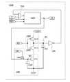
次に、図2(B)に示す半導体装置の点Aから点Bにかけてのバンド図の例を図1に示
す。図中、Evacは真空準位のエネルギー、Ecは伝導帯下端のエネルギー、Evは価
電子帯上端のエネルギーを示す。Next, FIG. 1 shows an example of a band diagram from point A to point B of the semiconductor device shown in FIG. 2 (B). In the figure, Evac indicates the energy of the vacuum level, Ec indicates the energy of the lower end of the conduction band, and Ev indicates the energy of the upper end of the valence band.
この例では、酸化物半導体膜104にIn:Ga:Zn:O=1:1:1:4(原子数
比)の酸化物半導体膜を、ゲート絶縁膜108aに酸化ハフニウム膜を、ゲート絶縁膜1
08bに酸化窒化シリコン膜を用いている。In this example, the
A silicon oxide nitride film is used for 08b.
図1に示すように酸化物半導体膜104のバンドギャップ(3.2eV)はゲート絶縁
膜108aのバンドギャップ(5.5eV)よりも小さく、ゲート絶縁膜108aのバン
ドギャップ(5.5eV)はゲート絶縁膜108bのバンドギャップ(8.7eV)より
も小さい。また、酸化物半導体膜104の電子親和力(4.7eV)はゲート絶縁膜10
8aの電子親和力(2.8eV)よりも大きく、ゲート絶縁膜108aの電子親和力(2
.8eV)はゲート絶縁膜108bの電子親和力(1.1eV)よりも大きい。As shown in FIG. 1, the band gap (3.2 eV) of the
The electron affinity (2) of the
.. 8eV) is larger than the electron affinity (1.1eV) of the
図1に示すように酸化物半導体膜104、ゲート絶縁膜108aおよびゲート絶縁膜1
08bにおいて、伝導帯下端のエネルギーはゲート絶縁膜108bが最も高く、酸化物半
導体膜104が最も低い。As shown in FIG. 1, the
In 08b, the energy at the lower end of the conduction band is highest in the
このようなバンド構造をとることにより、FETの導通時における、ゲート絶縁膜10
8a(High−k絶縁膜)とゲート絶縁膜108b(酸化シリコン膜や酸化窒化シリコ
ン膜)との界面のキャリア密度を低減できるため、該界面の界面準位密度によらず、オン
電流の向上やS値の減少等の安定した電気特性を得ることができる。By adopting such a band structure, the
Since the carrier density at the interface between the 8a (High-k insulating film) and the
また、詳細は次の実施の形態で説明するが、酸化物半導体膜104の上下に別の酸化物
半導体膜を設けた構成(実施の形態2の酸化物半導体層404に相当)にすると好ましい
。チャネルが形成される酸化物半導体膜104とゲート絶縁膜108aの間に別の酸化物
半導体膜を設けることでチャネルとなる領域をゲート絶縁膜108aから離すことができ
、酸化物半導体膜104の上側の酸化物半導体膜(実施の形態2の酸化物半導体膜404
cに相当)とゲート絶縁膜108aとの界面で起こるキャリアの散乱の影響を小さくする
ことができる。Although details will be described in the next embodiment, it is preferable to have a configuration in which another oxide semiconductor film is provided above and below the oxide semiconductor film 104 (corresponding to the
It is possible to reduce the influence of carrier scattering that occurs at the interface between (corresponding to c) and the
以上、本実施の形態に示す構成、方法などは、他の実施の形態に示す構成、方法などと
適宜組み合わせて用いることができる。As described above, the configurations and methods shown in the present embodiment can be appropriately combined with the configurations and methods shown in other embodiments.
(実施の形態2)
本実施の形態では、本発明の一態様の半導体装置について図面を用いて説明する。(Embodiment 2)
In the present embodiment, the semiconductor device of one aspect of the present invention will be described with reference to the drawings.
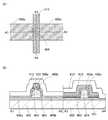
<トランジスタ構造1>
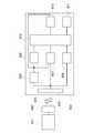
図3(A)および図3(B)は、本発明の一態様のトランジスタの上面図および断面図
である。図3(A)は上面図であり、図3(B)は、図3(A)に示す一点鎖線A1−A
2、および一点鎖線A3−A4に対応する断面図である。なお、図3(A)の上面図では
、図の明瞭化のために一部の要素を省いて図示している。また、図3(B)の酸化物半導
体層404の拡大図を図3(C)に示す。<
3 (A) and 3 (B) are a top view and a cross-sectional view of a transistor according to an aspect of the present invention. 3 (A) is a top view, and FIG. 3 (B) is the alternate long and short dash line A1-A shown in FIG. 3 (A).
2 is a cross-sectional view corresponding to 2 and the alternate long and short dash line A3-A4. In the top view of FIG. 3A, some elements are omitted for the sake of clarity of the figure. Further, an enlarged view of the
図3に示すトランジスタは、基板400上の凸部を有する下地絶縁膜402と、下地絶
縁膜402の凸部上の酸化物半導体膜404aと、酸化物半導体膜404a上の酸化物半
導体膜404bと、酸化物半導体膜404bの上面および側面と接するソース電極406
aおよびドレイン電極406bと、酸化物半導体膜404b、ソース電極406a上およ
びドレイン電極406b上の酸化物半導体膜404cと、酸化物半導体膜404c上のゲ
ート絶縁膜408aと、ゲート絶縁膜408a上のゲート絶縁膜408bと、ゲート絶縁
膜408bの上面に接し、酸化物半導体膜404bの上面および側面に面するゲート電極
410と、ソース電極406a、ドレイン電極406bおよびゲート電極410上の絶縁
膜412と、を有する。なお、下地絶縁膜402が凸部を有さなくても構わない。なお、
図3(C)示すように酸化物半導体膜404a、酸化物半導体膜404b、および酸化物
半導体膜404cをまとめて酸化物半導体層404と呼ぶことがある。The transistors shown in FIG. 3 include an underlying
a and the
As shown in FIG. 3C, the
なお、ソース電極406a(および/または、ドレイン電極406b)の、少なくとも
一部(または全部)は、酸化物半導体膜404a(および/または、酸化物半導体膜40
4b)などの半導体膜の、表面、側面、上面、および/または、下面の少なくとも一部(
または全部)に設けられている。At least a part (or all) of the source electrode 406a (and / or the
At least a portion (4b) of a surface, side surface, top surface, and / or bottom surface of a semiconductor film such as (4b).
Or all).
または、ソース電極406a(および/または、ドレイン電極406b)の、少なくと
も一部(または全部)は、酸化物半導体膜404a(および/または、酸化物半導体膜4
04b)などの半導体膜の、表面、側面、上面、および/または、下面の少なくとも一部
(または全部)と、接している。または、ソース電極406a(および/または、ドレイ
ン電極406b)の、少なくとも一部(または全部)は、酸化物半導体膜404a(およ
び/または、酸化物半導体膜404b)などの半導体膜の少なくとも一部(または全部)
と、接している。Alternatively, at least a part (or all) of the source electrode 406a (and / or the
It is in contact with at least a part (or all) of the surface, side surface, upper surface, and / or lower surface of a semiconductor film such as 04b). Alternatively, at least a part (or all) of the source electrode 406a (and / or the
I am in contact with you.
または、ソース電極406a(および/または、ドレイン電極406b)の、少なくと
も一部(または全部)は、酸化物半導体膜404a(および/または、酸化物半導体膜4
04b)などの半導体膜の、表面、側面、上面、および/または、下面の少なくとも一部
(または全部)と、電気的に接続されている。または、ソース電極406a(および/ま
たは、ドレイン電極406b)の、少なくとも一部(または全部)は、酸化物半導体膜4
04a(および/または、酸化物半導体膜404b)などの半導体膜の一部(または全部
)と、電気的に接続されている。Alternatively, at least a part (or all) of the source electrode 406a (and / or the
It is electrically connected to at least a part (or all) of the surface, side surface, upper surface, and / or lower surface of a semiconductor film such as 04b). Alternatively, at least a part (or all) of the source electrode 406a (and / or the
It is electrically connected to a part (or all) of a semiconductor film such as 04a (and / or an
または、ソース電極406a(および/または、ドレイン電極406b)の、少なくと
も一部(または全部)は、酸化物半導体膜404a(および/または、酸化物半導体膜4
04b)などの半導体膜の、表面、側面、上面、および/または、下面の少なくとも一部
(または全部)に、近接して配置されている。または、ソース電極406a(および/ま
たは、ドレイン電極406b)の、少なくとも一部(または全部)は、酸化物半導体膜4
04a(および/または、酸化物半導体膜404b)などの半導体膜の一部(または全部
)に、近接して配置されている。Alternatively, at least a part (or all) of the source electrode 406a (and / or the
It is arranged in close proximity to at least a part (or all) of the surface, side surface, upper surface, and / or lower surface of a semiconductor film such as 04b). Alternatively, at least a part (or all) of the source electrode 406a (and / or the
It is arranged in close proximity to a part (or all) of a semiconductor film such as 04a (and / or an
または、ソース電極406a(および/または、ドレイン電極406b)の、少なくと
も一部(または全部)は、酸化物半導体膜404a(および/または、酸化物半導体膜4
04b)などの半導体膜の、表面、側面、上面、および/または、下面の少なくとも一部
(または全部)の横側に配置されている。または、ソース電極406a(および/または
、ドレイン電極406b)の、少なくとも一部(または全部)は、酸化物半導体膜404
a(および/または、酸化物半導体膜404b)などの半導体膜の一部(または全部)の
横側に配置されている。Alternatively, at least a part (or all) of the source electrode 406a (and / or the
It is arranged on the lateral side of at least a part (or all) of the surface, the side surface, the upper surface, and / or the lower surface of the semiconductor film such as 04b). Alternatively, at least a part (or all) of the source electrode 406a (and / or the
It is arranged on the lateral side of a part (or all) of a semiconductor film such as a (and / or an
または、ソース電極406a(および/または、ドレイン電極406b)の、少なくと
も一部(または全部)は、酸化物半導体膜404a(および/または、酸化物半導体膜4
04b)などの半導体膜の、表面、側面、上面、および/または、下面の少なくとも一部
(または全部)の斜め上側に配置されている。または、ソース電極406a(および/ま
たは、ドレイン電極406b)の、少なくとも一部(または全部)は、酸化物半導体膜4
04a(および/または、酸化物半導体膜404b)などの半導体膜の一部(または全部
)の斜め上側に配置されている。Alternatively, at least a part (or all) of the source electrode 406a (and / or the
It is disposed obliquely above the surface, side surface, upper surface, and / or at least a part (or all) of the lower surface of a semiconductor film such as 04b). Alternatively, at least a part (or all) of the source electrode 406a (and / or the
It is arranged diagonally above a part (or all) of a semiconductor film such as 04a (and / or an
または、ソース電極406a(および/または、ドレイン電極406b)の、少なくと
も一部(または全部)は、酸化物半導体膜404a(および/または、酸化物半導体膜4
04b)などの半導体膜の、表面、側面、上面、および/または、下面の少なくとも一部
(または全部)の上側に配置されている。または、ソース電極406a(および/または
、ドレイン電極406b)の、少なくとも一部(または全部)は、酸化物半導体膜404
a(および/または、酸化物半導体膜404b)などの半導体膜の一部(または全部)の
上側に配置されている。Alternatively, at least a part (or all) of the source electrode 406a (and / or the
It is disposed above the surface, side surface, upper surface, and / or at least a part (or all) of the lower surface of a semiconductor film such as 04b). Alternatively, at least a part (or all) of the source electrode 406a (and / or the
It is arranged above a part (or all) of a semiconductor film such as a (and / or an
図3(B)に示すように、ソース電極406aおよびドレイン電極406bの側面が酸
化物半導体層404の側面と接する。また、ゲート電極410の電界によって、酸化物半
導体層404を電気的に取り囲むことができる(ゲート電極の電界によって、酸化物半導
体層を電気的に取り囲むトランジスタの構造を、surrounded channel
(s−channel)構造とよぶ。)。そのため、酸化物半導体層404の全体(バル
ク)にチャネルが形成される。s−channel構造では、トランジスタのソース−ド
レイン間に大電流を流すことができ、高いオン電流を得ることができる。As shown in FIG. 3B, the side surfaces of the
It is called a (s-channel) structure. ). Therefore, a channel is formed in the entire (bulk) of the
高いオン電流が得られるため、s−channel構造は、微細化されたトランジスタ
に適した構造といえる。トランジスタを微細化できるため、該トランジスタを有する半導
体装置は、集積度の高い、高密度化された半導体装置とすることが可能となる。例えば、
トランジスタのチャネル長を、好ましくは40nm以下、さらに好ましくは30nm以下
、より好ましくは20nm以下とし、かつ、トランジスタのチャネル幅を、好ましくは4
0nm以下、さらに好ましくは30nm以下、より好ましくは20nm以下とする。Since a high on-current can be obtained, the s-channel structure can be said to be a structure suitable for miniaturized transistors. Since the transistor can be miniaturized, the semiconductor device having the transistor can be a high-density semiconductor device with a high degree of integration. for example,
The channel length of the transistor is preferably 40 nm or less, more preferably 30 nm or less, more preferably 20 nm or less, and the channel width of the transistor is preferably 4
It is 0 nm or less, more preferably 30 nm or less, and more preferably 20 nm or less.
なお、チャネル長とは、上面図において、半導体層とゲート電極とが重なる領域におけ
る、ソース(ソース領域またはソース電極)とドレイン(ドレイン領域またはドレイン電
極)との距離をいう。すなわち、図3(A)では、チャネル長は、酸化物半導体層404
とゲート電極410とが重なる領域における、ソース電極406aとドレイン電極406
bとの距離となる。チャネル幅とは、半導体層とゲート電極とが重なる領域における、ソ
ースまたはドレインの幅をいう。すなわち、図3(A)では、チャネル幅は、酸化物半導
体層404とゲート電極410とが重なる領域における、ソース電極406aまたはドレ
イン電極406bの幅をいう。The channel length refers to the distance between the source (source region or source electrode) and the drain (drain region or drain electrode) in the region where the semiconductor layer and the gate electrode overlap in the top view. That is, in FIG. 3A, the channel length is the
It is the distance from b. The channel width refers to the width of the source or drain in the region where the semiconductor layer and the gate electrode overlap. That is, in FIG. 3A, the channel width refers to the width of the
ゲート絶縁膜408aは、ゲート絶縁膜108aについての記載を参照する。なお、ゲ
ート絶縁膜408aは単層であっても積層であっても構わない。For the
ゲート絶縁膜408bは、ゲート絶縁膜108bについての記載を参照する。なお、ゲ
ート絶縁膜408bは単層であっても積層であっても構わない。For the
基板400は、単なる支持体に限らず、他のトランジスタやキャパシタなどの素子が形
成された基板であってもよい。この場合、トランジスタのゲート電極410、ソース電極
406a、ドレイン電極406bの少なくとも一つが、上記の他の素子と電気的に接続さ
れていてもよい。The
下地絶縁膜402は、基板400からの不純物の拡散を防止する役割を有するほか、酸
化物半導体層404に酸素を供給する役割を担うことができる。したがって、下地絶縁膜
402は酸素を含む絶縁膜であることが好ましい。例えば、化学量論的組成よりも多い酸
素を含む絶縁膜であることがより好ましい。また、上述のように基板400が他の素子が
形成された基板である場合、下地絶縁膜402は、層間絶縁膜としての機能も有する。そ
の場合、下地絶縁膜402の表面が平坦化されていてもよい。例えば、下地絶縁膜402
にCMP(Chemical Mechanical Polishing)法等で平坦
化処理を行えばよい。The underlying
The flattening process may be performed by a CMP (Chemical Mechanical Polishing) method or the like.
以下では、酸化物半導体膜404bについて詳細に説明する。 Hereinafter, the
酸化物半導体膜404bは、インジウムを含む酸化物である。酸化物は、例えば、イン
ジウムを含むと、キャリア移動度(電子移動度)が高くなる。また、酸化物半導体膜40
4bは、元素Mを含むと好ましい。元素Mとして、例えば、アルミニウム、ガリウム、イ
ットリウムまたはスズなどがある。元素Mは、例えば、酸素との結合エネルギーが高い元
素である。元素Mは、例えば、酸化物のバンドギャップを大きくする機能を有する元素で
ある。また、酸化物半導体膜404bは、亜鉛を含むと好ましい。酸化物が亜鉛を含むと
、例えば、酸化物を結晶化しやすくなる。酸化物の価電子帯上端のエネルギーは、例えば
、亜鉛の原子数比によって制御できる。The
4b preferably contains the element M. The element M includes, for example, aluminum, gallium, yttrium, tin and the like. The element M is, for example, an element having a high binding energy with oxygen. The element M is, for example, an element having a function of increasing the band gap of the oxide. Further, it is preferable that the
ただし、酸化物半導体膜404bは、インジウムを含む酸化物に限定されない。酸化物
半導体膜404bは、例えば、Zn−Sn酸化物、Ga−Sn酸化物であっても構わない
。However, the
また、酸化物半導体膜404bは、バンドギャップが大きい酸化物を用いる。酸化物半
導体膜404bのバンドギャップは、例えば、2.5eV以上4.2eV以下、好ましく
は2.8eV以上3.8eV以下、さらに好ましくは3.0eV以上3.5eV以下とす
る。Further, the
なお、酸化物半導体膜404bをスパッタリング法で成膜する場合、パーティクル数低
減のため、インジウムを含むターゲットを用いると好ましい。また、元素Mの原子数比が
高い酸化物ターゲットを用いた場合、ターゲットの導電性が低くなる場合がある。インジ
ウムを含むターゲットを用いる場合、ターゲットの導電率を高めることができ、DC放電
、AC放電が容易となるため、大面積の基板へ対応しやすくなる。したがって、半導体装
置の生産性を高めることができる。When the
酸化物半導体膜404bをスパッタリング法で成膜する場合、ターゲットの原子数比は
、In:M:Znが3:1:1、3:1:2、3:1:4、1:1:0.5、1:1:1
、1:1:2、などとすればよい。When the
, 1: 1: 2, and so on.
酸化物半導体膜404bをスパッタリング法で成膜する場合、ターゲットの原子数比か
らずれた原子数比の膜が形成される場合がある。特に、亜鉛は、ターゲットの原子数比よ
りも膜の原子数比が小さくなる場合がある。具体的には、ターゲットに含まれる亜鉛の原
子数比の40atomic%以上90atomic%程度以下となる場合がある。When the
以下では、酸化物半導体膜404b中における不純物の影響について説明する。なお、
トランジスタの電気特性を安定にするためには、酸化物半導体膜404b中の不純物濃度
を低減し、低キャリア密度化および高純度化することが有効である。なお、酸化物半導体
膜404bのキャリア密度は、1×10¹⁷個/cm3未満、1×1015個/cm3未
満、または1×10¹³個/cm3未満とする。酸化物半導体膜404b中の不純物濃度
を低減するためには、近接する膜中の不純物濃度も低減することが好ましい。Hereinafter, the influence of impurities in the
In order to stabilize the electrical characteristics of the transistor, it is effective to reduce the impurity concentration in the
例えば、酸化物半導体膜404b中のシリコンは、キャリアトラップやキャリア発生源
となる場合がある。そのため、酸化物半導体膜404bと下地絶縁膜402との間におけ
るシリコン濃度を、二次イオン質量分析法(SIMS:Secondary Ion M
ass Spectrometry)において、1×10¹⁹atoms/cm3未満、
好ましくは5×10¹⁸atoms/cm3未満、さらに好ましくは2×1018ato
ms/cm3未満とする。また、酸化物半導体膜404bとゲート絶縁膜408aとの間
におけるシリコン濃度を、SIMSにおいて、1×10¹⁹atoms/cm3未満、好
ましくは5×10¹⁸atoms/cm3未満、さらに好ましくは2×1018atom
s/cm3未満とする。For example, silicon in the
In ass Spectrometry), less than1 × 10 19 atoms / cm3,
Preferably less than 5 × 10¹⁸ atoms / cm3 , more preferably 2 × 10¹⁸ ato
It shall be less than ms / cm3. Further, the silicon concentration between the
It shall be less than s / cm3.
また、酸化物半導体膜404b中に水素が含まれると、キャリア密度を増大させてしま
う場合がある。酸化物半導体膜404bの水素濃度はSIMSにおいて、2×10²⁰a
toms/cm3以下、好ましくは5×1019atoms/cm3以下、より好ましく
は1×10¹⁹atoms/cm3以下、さらに好ましくは5×1018atoms/c
m3以下とする。また、酸化物半導体膜404b中に窒素が含まれると、キャリア密度を
増大させてしまう場合がある。酸化物半導体膜404bの窒素濃度は、SIMSにおいて
、5×10¹⁹atoms/cm3未満、好ましくは5×1018atoms/cm3以
下、より好ましくは1×10¹⁸atoms/cm3以下、さらに好ましくは5×101
7atoms/cm3以下とする。Further, if hydrogen is contained in the
toms / cm3 or less, preferably 5 × 10¹⁹ atoms / cm3 or less, more preferably 1 × 10¹⁹ atoms / cm3 or less, still more preferably 5 × 10¹⁸ atoms / c.
It shall be m3 or less. Further, if nitrogen is contained in the
7 atoms / cm3 or less.
また、酸化物半導体膜404bの水素濃度を低減するために、下地絶縁膜402の水素
濃度を低減すると好ましい。下地絶縁膜402の水素濃度はSIMSにおいて、2×10
20atoms/cm3以下、好ましくは5×1019atoms/cm3以下、より好
ましくは1×10¹⁹atoms/cm3以下、さらに好ましくは5×1018atom
s/cm3以下とする。また、酸化物半導体膜404bの窒素濃度を低減するために、下
地絶縁膜402の窒素濃度を低減すると好ましい。下地絶縁膜402の窒素濃度は、SI
MSにおいて、5×10¹⁹atoms/cm3未満、好ましくは5×1018atom
s/cm3以下、より好ましくは1×1018atoms/cm3以下、さらに好ましく
は5×10¹⁷atoms/cm3以下とする。Further, in order to reduce the hydrogen concentration of the
20 atoms / cm3 or less, preferably 5 × 10¹⁹ atoms / cm3 or less, more preferably 1 × 10¹⁹ atoms / cm3 or less, still more preferably 5 × 10¹⁸ atom.
It shall be s / cm3 or less. Further, in order to reduce the nitrogen concentration of the
In MS,less than 5 × 10 19 atoms / cm3 , preferably 5 × 10¹⁸ atoms
It is s / cm3 or less, more preferably 1 × 10¹⁸ atoms / cm3 or less, and further preferably 5 × 10¹⁷ atoms / cm3 or less.
また、酸化物半導体膜404bの水素濃度を低減するために、ゲート絶縁膜408aの
水素濃度を低減すると好ましい。ゲート絶縁膜408aの水素濃度はSIMSにおいて、
2×10²⁰atoms/cm3以下、好ましくは5×1019atoms/cm3以下
、より好ましくは1×10¹⁹atoms/cm3以下、さらに好ましくは5×1018
atoms/cm3以下とする。また、酸化物半導体膜404bの窒素濃度を低減するた
めに、ゲート絶縁膜408aの窒素濃度を低減すると好ましい。ゲート絶縁膜408aの
窒素濃度は、SIMSにおいて、5×10¹⁹atoms/cm3未満、好ましくは5×
1018atoms/cm3以下、より好ましくは1×1018atoms/cm3以下
、さらに好ましくは5×10¹⁷atoms/cm3以下とする。Further, in order to reduce the hydrogen concentration of the
2 × 10²⁰ atoms / cm3 or less, preferably 5 × 10¹⁹ atoms / cm3 or less, more preferably 1 × 10¹⁹ atoms / cm3 or less, still more preferably 5 × 10¹⁸
Atoms / cm3 or less. Further, in order to reduce the nitrogen concentration of the
It is 1018 atoms / cm3 or less, more preferably 1 × 10¹⁸ atoms / cm3 or less, and further preferably 5 × 10¹⁷ atoms / cm3 or less.
以下では、酸化物半導体膜404bに適用可能な酸化物半導体膜の構造について説明す
る。Hereinafter, the structure of the oxide semiconductor film applicable to the
酸化物半導体膜は、非単結晶酸化物半導体膜と単結晶酸化物半導体膜とに大別される。
非単結晶酸化物半導体膜とは、CAAC−OS(C Axis Aligned Cry
stalline Oxide Semiconductor)膜、多結晶酸化物半導体
膜、微結晶酸化物半導体膜、非晶質酸化物半導体膜などをいう。Oxide semiconductor films are roughly classified into non-single crystal oxide semiconductor films and single crystal oxide semiconductor films.
The non-single crystal oxide semiconductor film is CAAC-OS (C Axis Aligned Cry).
Stallline Oxide Semiconductor) film, polycrystalline oxide semiconductor film, microcrystalline oxide semiconductor film, amorphous oxide semiconductor film, etc.
まずは、CAAC−OS膜について説明する。 First, the CAAC-OS film will be described.
CAAC−OS膜は、複数の結晶部を有する酸化物半導体膜の一つであり、ほとんどの
結晶部は、一辺が100nm未満の立方体内に収まる大きさである。したがって、CAA
C−OS膜に含まれる結晶部は、一辺が10nm未満、5nm未満または3nm未満の立
方体内に収まる大きさの場合も含まれる。The CAAC-OS film is one of the oxide semiconductor films having a plurality of crystal portions, and most of the crystal portions have a size that can be accommodated in a cube having a side of less than 100 nm. Therefore, CAA
The crystal portion contained in the C-OS film may have a size of less than 10 nm on a side and a size of less than 5 nm or less than 3 nm within a cube.
CAAC−OS膜を透過型電子顕微鏡(TEM:Transmission Elec
tron Microscope)によって観察すると、明確な結晶部同士の境界、即ち
結晶粒界(グレインバウンダリーともいう。)を確認することができない。そのため、C
AAC−OS膜は、結晶粒界に起因する電子移動度の低下が起こりにくいといえる。Transmission electron microscope (TEM: Transmission Elec) through CAAC-OS membrane
When observed by a TRON Microscope), it is not possible to confirm a clear boundary between crystal portions, that is, a grain boundary (also referred to as a grain boundary). Therefore, C
It can be said that the AAC-OS film is unlikely to cause a decrease in electron mobility due to grain boundaries.
CAAC−OS膜を、試料面と概略平行な方向からTEMによって観察(断面TEM観
察)すると、結晶部において、金属原子が層状に配列していることを確認できる。金属原
子の各層は、CAAC−OS膜を形成する面(被形成面ともいう。)または上面の凹凸を
反映した形状であり、CAAC−OS膜の被形成面または上面と平行に配列する。When the CAAC-OS film is observed by TEM from a direction substantially parallel to the sample surface (cross-section TEM observation), it can be confirmed that the metal atoms are arranged in layers in the crystal portion. Each layer of the metal atom has a shape that reflects the unevenness of the surface (also referred to as the formed surface) or the upper surface on which the CAAC-OS film is formed, and is arranged in parallel with the formed surface or the upper surface of the CAAC-OS film.
一方、CAAC−OS膜を、試料面と概略垂直な方向からTEMによって観察(平面T
EM観察)すると、結晶部において、金属原子が三角形状または六角形状に配列している
ことを確認できる。しかしながら、異なる結晶部間で、金属原子の配列に規則性は見られ
ない。On the other hand, the CAAC-OS film is observed by TEM from a direction substantially perpendicular to the sample surface (plane T).
By EM observation), it can be confirmed that the metal atoms are arranged in a triangular shape or a hexagonal shape in the crystal portion. However, there is no regularity in the arrangement of metal atoms between different crystal parts.
なお、CAAC−OS膜に対し、電子回折を行うと、配向性を示すスポット(輝点)が
観測される。例えば、CAAC−OS膜の上面に対し、例えば1nm以上30nm以下の
電子線を用いる電子回折(ナノビーム電子回折ともいう。)を行うと、スポットが観測さ
れる(図30(A)参照。)。When electron diffraction is performed on the CAAC-OS film, spots (bright spots) showing orientation are observed. For example, when electron diffraction (also referred to as nanobeam electron diffraction) using an electron beam of 1 nm or more and 30 nm or less is performed on the upper surface of the CAAC-OS film, spots are observed (see FIG. 30 (A)).
断面TEM観察および平面TEM観察より、CAAC−OS膜の結晶部は配向性を有し
ていることがわかる。From the cross-sectional TEM observation and the planar TEM observation, it can be seen that the crystal portion of the CAAC-OS film has orientation.
CAAC−OS膜に対し、X線回折(XRD:X−Ray Diffraction)
装置を用いて構造解析を行うと、例えばInGaZnO4の結晶を有するCAAC−OS
膜のout−of−plane法による解析では、回折角(2θ)が31°近傍にピーク
が現れる場合がある。このピークは、InGaZnO4の結晶の(009)面に帰属され
ることから、CAAC−OS膜の結晶がc軸配向性を有し、c軸が被形成面または上面に
概略垂直な方向を向いていることが確認できる。X-ray diffraction (XRD: X-Ray Diffraction) with respect to the CAAC-OS film
When structural analysis is performed using the device, for example, CAAC-OS having crystals ofInGaZnO 4
In the analysis of the film by the out-of-plane method, a peak may appear in the vicinity of the diffraction angle (2θ) of 31 °. Since this peak isattributed to the (009) plane of the InGaZnO 4 crystal, the crystal of the CAAC-OS film has c-axis orientation, and the c-axis is oriented substantially perpendicular to the surface to be formed or the upper surface. It can be confirmed that it is.
なお、本明細書において、結晶が三方晶または菱面体晶である場合、六方晶系として表
す。In the present specification, when the crystal is a trigonal crystal or a rhombohedral crystal, it is represented as a hexagonal system.
一方、CAAC−OS膜に対し、c軸に概略垂直な方向からX線を入射させるin−p
lane法による解析では、2θが56°近傍にピークが現れる場合がある。このピーク
は、InGaZnO4の結晶の(110)面に帰属される。InGaZnO4の単結晶酸
化物半導体膜であれば、2θを56°近傍に固定し、試料面の法線ベクトルを軸(φ軸)
として試料を回転させながら分析(φスキャン)を行うと、(110)面と等価な結晶面
に帰属されるピークが6本観察される。これに対し、CAAC−OS膜の場合は、2θを
56°近傍に固定してφスキャンした場合でも、明瞭なピークが現れない。On the other hand, in-p in which X-rays are incident on the CAAC-OS film from a direction substantially perpendicular to the c-axis.
In the analysis by the lane method, a peak may appear near 56 ° in 2θ. This peak is attributed to the (110) plane of the crystal ofInGaZnO 4. In the case ofa single crystal oxide semiconductor film of InGaZnO 4 , 2θ is fixed in the vicinity of 56 °, and the normal vector of the sample surface is the axis (φ axis).
When the analysis (φ scan) is performed while rotating the sample, 6 peaks attributed to the crystal plane equivalent to the (110) plane are observed. On the other hand, in the case of the CAAC-OS film, a clear peak does not appear even when 2θ is fixed in the vicinity of 56 ° and φ scan is performed.
以上のことから、CAAC−OS膜では、異なる結晶部間ではa軸およびb軸の配向は
不規則であるが、c軸配向性を有し、かつc軸が被形成面または上面の法線ベクトルに平
行な方向を向いていることがわかる。したがって、前述の断面TEM観察で確認された層
状に配列した金属原子の各層は、結晶のab面に平行な面である。From the above, in the CAAC-OS film, the orientation of the a-axis and the b-axis is irregular between different crystal portions, but the orientation is c-axis, and the c-axis is the normal of the surface to be formed or the upper surface. It can be seen that the direction is parallel to the vector. Therefore, each layer of the metal atoms arranged in layers confirmed by the above-mentioned cross-sectional TEM observation is a plane parallel to the ab plane of the crystal.
なお、結晶部は、CAAC−OS膜を成膜した際、または加熱処理などの結晶化処理を
行った際に形成される。上述したように、結晶のc軸は、CAAC−OS膜の被形成面ま
たは上面の法線ベクトルに平行な方向に配向する。したがって、例えば、CAAC−OS
膜の形状をエッチングなどによって変化させた場合、結晶のc軸がCAAC−OS膜の被
形成面または上面の法線ベクトルと平行にならないこともある。The crystal portion is formed when a CAAC-OS film is formed or when a crystallization treatment such as a heat treatment is performed. As described above, the c-axis of the crystal is oriented in a direction parallel to the normal vector of the surface to be formed or the upper surface of the CAAC-OS film. Therefore, for example, CAAC-OS
When the shape of the film is changed by etching or the like, the c-axis of the crystal may not be parallel to the normal vector of the surface to be formed or the upper surface of the CAAC-OS film.
また、CAAC−OS膜中の結晶化度が均一でなくてもよい。例えば、CAAC−OS
膜の結晶部が、CAAC−OS膜の上面近傍からの結晶成長によって形成される場合、上
面近傍の領域は、被形成面近傍の領域よりも結晶化度が高くなることがある。また、CA
AC−OS膜に不純物を添加する場合、不純物が添加された領域の結晶化度が変化し、部
分的に結晶化度の異なる領域が形成されることもある。Further, the crystallinity in the CAAC-OS film does not have to be uniform. For example, CAAC-OS
When the crystal portion of the film is formed by crystal growth from the vicinity of the upper surface of the CAAC-OS film, the region near the upper surface may have a higher crystallinity than the region near the surface to be formed. Also, CA
When an impurity is added to the AC-OS film, the crystallinity of the region to which the impurity is added changes, and a region having a partially different crystallinity may be formed.
なお、InGaZnO4の結晶を有するCAAC−OS膜のout−of−plane
法による解析では、2θが31°近傍のピークの他に、2θが36°近傍にもピークが現
れる場合がある。2θが36°近傍のピークは、CAAC−OS膜中の一部に、c軸配向
性を有さない結晶が含まれることを示している。CAAC−OS膜は、2θが31°近傍
にピークを示し、2θが36°近傍にピークを示さないことが好ましい。The out-of-plane of the CAAC-OS film having InGaZnO4 crystals.
In the analysis by the method, in addition to the peak near 31 ° in 2θ, the peak may appear near 36 ° in 2θ. The peak in which 2θ is in the vicinity of 36 ° indicates that a part of the CAAC-OS film contains crystals having no c-axis orientation. In the CAAC-OS film, it is preferable that 2θ shows a peak near 31 ° and 2θ does not show a peak near 36 °.
CAAC−OS膜は、不純物濃度の低い酸化物半導体膜である。不純物は、水素、炭素
、シリコン、遷移金属元素などの酸化物半導体膜の主成分以外の元素である。特に、シリ
コンなどの、酸化物半導体膜を構成する金属元素よりも酸素との結合力の強い元素は、酸
化物半導体膜から酸素を奪うことで酸化物半導体膜の原子配列を乱し、結晶性を低下させ
る要因となる。また、鉄やニッケルなどの重金属、アルゴン、二酸化炭素などは、原子半
径(または分子半径)が大きいため、酸化物半導体膜内部に含まれると、酸化物半導体膜
の原子配列を乱し、結晶性を低下させる要因となる。なお、酸化物半導体膜に含まれる不
純物は、キャリアトラップやキャリア発生源となる場合がある。The CAAC-OS film is an oxide semiconductor film having a low impurity concentration. Impurities are elements other than the main components of oxide semiconductor films such as hydrogen, carbon, silicon, and transition metal elements. In particular, elements such as silicon, which have a stronger bond with oxygen than the metal elements constituting the oxide semiconductor film, disturb the atomic arrangement of the oxide semiconductor film by depriving the oxide semiconductor film of oxygen and have crystalline properties. It becomes a factor to reduce. In addition, heavy metals such as iron and nickel, argon, carbon dioxide, etc. have a large atomic radius (or molecular radius), so if they are contained inside the oxide semiconductor film, they disturb the atomic arrangement of the oxide semiconductor film and become crystalline. It becomes a factor to reduce. In addition, impurities contained in the oxide semiconductor film may become a carrier trap or a carrier generation source.
また、CAAC−OS膜は、欠陥準位密度の低い酸化物半導体膜である。例えば、酸化
物半導体膜中の酸素欠損は、キャリアトラップとなることや、水素を捕獲することによっ
てキャリア発生源となることがある。The CAAC-OS film is an oxide semiconductor film having a low defect level density. For example, oxygen deficiency in an oxide semiconductor film may become a carrier trap or a carrier generation source by capturing hydrogen.
不純物濃度が低く、欠陥準位密度が低い(酸素欠損の少ない)ことを、高純度真性また
は実質的に高純度真性と呼ぶ。高純度真性または実質的に高純度真性である酸化物半導体
膜は、キャリア発生源が少ないため、キャリア密度を低くすることができる。したがって
、当該酸化物半導体膜を用いたトランジスタは、しきい値電圧がマイナスとなる電気特性
(ノーマリーオンともいう。)になることが少ない。また、高純度真性または実質的に高
純度真性である酸化物半導体膜は、キャリアトラップが少ない。そのため、当該酸化物半
導体膜を用いたトランジスタは、電気特性の変動が小さく、信頼性の高いトランジスタと
なる。なお、酸化物半導体膜のキャリアトラップに捕獲された電荷は、放出するまでに要
する時間が長く、あたかも固定電荷のように振る舞うことがある。そのため、不純物濃度
が高く、欠陥準位密度が高い酸化物半導体膜を用いたトランジスタは、電気特性が不安定
となる場合がある。A low impurity concentration and a low defect level density (less oxygen deficiency) is called high-purity intrinsic or substantially high-purity intrinsic. Oxide semiconductor films having high-purity intrinsics or substantially high-purity intrinsics have few carrier sources, so that the carrier density can be lowered. Therefore, the transistor using the oxide semiconductor film rarely has electrical characteristics (also referred to as normally on) in which the threshold voltage becomes negative. Further, the oxide semiconductor film having high purity intrinsicity or substantially high purity intrinsicity has few carrier traps. Therefore, the transistor using the oxide semiconductor film has a small fluctuation in electrical characteristics and is a highly reliable transistor. The charge captured by the carrier trap of the oxide semiconductor film takes a long time to be released, and may behave as if it were a fixed charge. Therefore, a transistor using an oxide semiconductor film having a high impurity concentration and a high defect level density may have unstable electrical characteristics.
また、CAAC−OS膜を用いたトランジスタは、可視光や紫外光の照射による電気特
性の変動が小さい。Further, the transistor using the CAAC-OS film has a small fluctuation in electrical characteristics due to irradiation with visible light or ultraviolet light.
次に、微結晶酸化物半導体膜について説明する。 Next, the microcrystalline oxide semiconductor film will be described.
微結晶酸化物半導体膜は、TEMによる観察像では、明確に結晶部を確認することがで
きない場合がある。微結晶酸化物半導体膜に含まれる結晶部は、1nm以上100nm以
下、または1nm以上10nm以下の大きさであることが多い。特に、1nm以上10n
m以下、または1nm以上3nm以下の微結晶であるナノ結晶(nc:nanocrys
tal)を有する酸化物半導体膜を、nc−OS(nanocrystalline O
xide Semiconductor)膜と呼ぶ。また、nc−OS膜は、例えば、T
EMによる観察像では、結晶粒界を明確に確認できない場合がある。In the microcrystal oxide semiconductor film, the crystal portion may not be clearly confirmed in the observation image by TEM. The crystal part contained in the microcrystalline oxide semiconductor film often has a size of 1 nm or more and 100 nm or less, or 1 nm or more and 10 nm or less. In particular, 1 nm or more and 10 n
Nanocrystals (nc: nanocrys) that are microcrystals of m or less, or 1 nm or more and 3 nm or less.
An oxide semiconductor film having tal) is used as an nc-OS (nanocrystalline O).
It is called a xide Semiconductor) membrane. Further, the nc-OS film is, for example, T.
It may not be possible to clearly confirm the grain boundaries in the observation image by EM.
nc−OS膜は、微小な領域(例えば、1nm以上10nm以下の領域、特に1nm以
上3nm以下の領域)において原子配列に周期性を有する。また、nc−OS膜は、異な
る結晶部間で結晶方位に規則性が見られない。そのため、全体で配向性が見られない。し
たがって、nc−OS膜は、分析方法によっては、非晶質酸化物半導体膜と区別が付かな
い場合がある。例えば、nc−OS膜に対し、結晶部よりも大きい径のX線を用いるXR
D装置を用いて構造解析を行うと、out−of−plane法による解析では、結晶面
を示すピークが検出されない。また、nc−OS膜は、結晶部よりも大きいプローブ径(
例えば50nm以上)の電子線を用いる電子回折(制限視野電子回折ともいう。)を行う
と、ハローパターンのような回折パターンが観測される。一方、nc−OS膜に対し、結
晶部の大きさと近いか結晶部より小さいプローブ径の電子線を用いるナノビーム電子回折
を行うと、スポットが観測される。また、nc−OS膜に対しナノビーム電子回折を行う
と、円を描くように(リング状に)輝度の高い領域が観測される場合がある。また、nc
−OS膜に対しナノビーム電子回折を行うと、リング状の領域内に複数のスポットが観測
される場合がある(図30(B)参照。)。The nc-OS film has periodicity in the atomic arrangement in a minute region (for example, a region of 1 nm or more and 10 nm or less, particularly a region of 1 nm or more and 3 nm or less). In addition, the nc-OS film does not show regularity in crystal orientation between different crystal portions. Therefore, no orientation is seen as a whole. Therefore, the nc-OS film may be indistinguishable from the amorphous oxide semiconductor film depending on the analysis method. For example, XR using X-rays with a diameter larger than that of the crystal part for the nc-OS film.
When the structural analysis is performed using the D apparatus, the peak indicating the crystal plane is not detected in the analysis by the out-of-plane method. Further, the nc-OS film has a probe diameter larger than that of the crystal portion (
When electron diffraction (also referred to as selected area electron diffraction) using an electron beam having a diameter of 50 nm or more is performed, a diffraction pattern such as a halo pattern is observed. On the other hand, when nanobeam electron diffraction is performed on the nc-OS film using an electron beam having a probe diameter close to the size of the crystal portion or smaller than the crystal portion, spots are observed. Further, when nanobeam electron diffraction is performed on the nc-OS film, a region having high brightness (in a ring shape) may be observed in a circular motion. Also, nc
-When nanobeam electron diffraction is performed on the OS film, a plurality of spots may be observed in the ring-shaped region (see FIG. 30 (B)).
nc−OS膜は、非晶質酸化物半導体膜よりも規則性の高い酸化物半導体膜である。そ
のため、nc−OS膜は、非晶質酸化物半導体膜よりも欠陥準位密度が低くなる。ただし
、nc−OS膜は、異なる結晶部間で結晶方位に規則性が見られない。そのため、nc−
OS膜は、CAAC−OS膜と比べて欠陥準位密度が高くなる。The nc-OS film is an oxide semiconductor film having higher regularity than the amorphous oxide semiconductor film. Therefore, the nc-OS film has a lower defect level density than the amorphous oxide semiconductor film. However, in the nc-OS film, there is no regularity in the crystal orientation between different crystal portions. Therefore, nc-
The OS film has a higher defect level density than the CAAC-OS film.
なお、酸化物半導体膜は、例えば、非晶質酸化物半導体膜、微結晶酸化物半導体膜、C
AAC−OS膜のうち、二種以上を有してもよい。The oxide semiconductor film may be, for example, an amorphous oxide semiconductor film, a microcrystalline oxide semiconductor film, or C.
You may have two or more kinds of AAC-OS films.
酸化物半導体膜が複数の構造を有する場合、ナノビーム電子回折を用いることで構造解
析が可能となる場合がある。When the oxide semiconductor film has a plurality of structures, structural analysis may be possible by using nanobeam electron diffraction.
図31(A)に、電子銃室10と、電子銃室10の下の光学系12と、光学系12の下
の試料室14と、試料室14の下の光学系16と、光学系16の下の観察室20と、観察
室20に設置されたカメラ18と、観察室20の下のフィルム室22と、を有する透過電
子回折測定装置を示す。カメラ18は、観察室20内部に向けて設置される。なお、フィ
ルム室22を有さなくても構わない。In FIG. 31A, the
また、図31(B)に、図31(A)で示した透過電子回折測定装置内部の構造を示す
。透過電子回折測定装置内部では、電子銃室10に設置された電子銃から放出された電子
が、光学系12を介して試料室14に配置された物質28に照射される。物質28を通過
した電子は、光学系16を介して観察室20内部に設置された蛍光板32に入射する。蛍
光板32では、入射した電子の強度に応じたパターンが現れることで透過電子回折パター
ンを測定することができる。Further, FIG. 31 (B) shows the internal structure of the transmitted electron diffraction measuring device shown in FIG. 31 (A). Inside the transmitted electron diffraction measuring device, the electrons emitted from the electron gun installed in the
カメラ18は、蛍光板32を向いて設置されており、蛍光板32に現れたパターンを撮
影することが可能である。カメラ18のレンズの中央、および蛍光板32の中央を通る直
線と、蛍光板32の上面と、の為す角度は、例えば、15°以上80°以下、30°以上
75°以下、または45°以上70°以下とする。該角度が小さいほど、カメラ18で撮
影される透過電子回折パターンは歪みが大きくなる。ただし、あらかじめ該角度がわかっ
ていれば、得られた透過電子回折パターンの歪みを補正することも可能である。なお、カ
メラ18をフィルム室22に設置しても構わない場合がある。例えば、カメラ18をフィ
ルム室22に、電子24の入射方向と対向するように設置してもよい。この場合、蛍光板
32の裏面から歪みの少ない透過電子回折パターンを撮影することができる。The
試料室14には、試料である物質28を固定するためのホルダが設置されている。ホル
ダは、物質28を通過する電子を透過するような構造をしている。ホルダは、例えば、物
質28をX軸、Y軸、Z軸などに移動させる機能を有していてもよい。ホルダの移動機能
は、例えば、1nm以上10nm以下、5nm以上50nm以下、10nm以上100n
m以下、50nm以上500nm以下、100nm以上1μm以下などの範囲で移動させ
る精度を有すればよい。これらの範囲は、物質28の構造によって最適な範囲を設定すれ
ばよい。In the
It suffices to have an accuracy of moving within a range of m or less, 50 nm or more and 500 nm or less, 100 nm or more and 1 μm or less. These ranges may be set to the optimum range according to the structure of the
次に、上述した透過電子回折測定装置を用いて、物質の透過電子回折パターンを測定す
る方法について説明する。Next, a method of measuring the transmitted electron diffraction pattern of a substance using the above-mentioned transmitted electron diffraction measuring device will be described.
例えば、図31(B)に示すように物質におけるナノビームである電子24の照射位置
を変化させる(スキャンする)ことで、物質の構造が変化していく様子を確認することが
できる。このとき、物質28がCAAC−OS膜であれば、図30(A)に示したような
回折パターンが観測される。または、物質28がnc−OS膜であれば、図30(B)に
示したような回折パターンが観測される。For example, as shown in FIG. 31 (B), by changing (scanning) the irradiation position of the
ところで、物質28がCAAC−OS膜であったとしても、部分的にnc−OS膜など
と同様の回折パターンが観測される場合がある。したがって、CAAC−OS膜の良否は
、一定の範囲におけるCAAC−OS膜の回折パターンが観測される領域の割合(CAA
C化率ともいう。)で表すことができる場合がある。例えば、良質なCAAC−OS膜で
あれば、CAAC化率は、60%以上、好ましくは80%以上、さらに好ましくは90%
以上、より好ましくは95%以上となる。なお、CAAC−OS膜と異なる回折パターン
が観測される領域の割合を非CAAC化率と表記する。By the way, even if the
Also called C conversion rate. ) May be expressed. For example, in the case of a high-quality CAAC-OS film, the CAAC conversion rate is 60% or more, preferably 80% or more, and more preferably 90%.
As mentioned above, it is more preferably 95% or more. The ratio of the region where a diffraction pattern different from that of the CAAC-OS film is observed is referred to as a non-CAAC conversion rate.
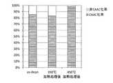
一例として、成膜直後(as−depoと表記。)、350℃加熱処理後または450
℃加熱処理後のCAAC−OS膜を有する各試料の上面に対し、スキャンしながら透過電
子回折パターンを取得した。ここでは、5nm/秒の速度で60秒間スキャンしながら回
折パターンを観測し、観測された回折パターンを0.5秒ごとに静止画に変換することで
、CAAC化率を導出した。なお、電子線としては、プローブ径が1nmのナノビーム電
子線を用いた。As an example, immediately after film formation (denoted as as-depo), after heat treatment at 350 ° C., or 450.
A transmitted electron diffraction pattern was obtained while scanning the upper surface of each sample having a CAAC-OS film after heat treatment at ° C. Here, the diffraction pattern was observed while scanning at a speed of 5 nm / sec for 60 seconds, and the observed diffraction pattern was converted into a still image every 0.5 seconds to derive the CAAC conversion rate. As the electron beam, a nanobeam electron beam having a probe diameter of 1 nm was used.
各試料におけるCAAC化率を図32に示す。成膜直後および350℃加熱処理後と比
べて、450℃加熱処理後のCAAC化率が高いことがわかる。即ち、350℃より高い
温度(例えば400℃以上)における加熱処理によって、非CAAC化率が低くなる(C
AAC化率が高くなる)ことがわかる。ここで、CAAC−OS膜と異なる回折パターン
のほとんどはnc−OS膜と同様の回折パターンであった。したがって、加熱処理によっ
て、nc−OS膜と同様の構造を有する領域は、隣接する領域の構造の影響を受けてCA
AC化していることが示唆される。The CAAC conversion rate in each sample is shown in FIG. 32. It can be seen that the CAAC conversion rate after the 450 ° C. heat treatment is higher than that immediately after the film formation and after the 350 ° C. heat treatment. That is, heat treatment at a temperature higher than 350 ° C. (for example, 400 ° C. or higher) lowers the non-CAAC conversion rate (C).
It can be seen that the AAC conversion rate is high). Here, most of the diffraction patterns different from the CAAC-OS film were the same diffraction patterns as the nc-OS film. Therefore, by heat treatment, the region having the same structure as the nc-OS film is affected by the structure of the adjacent region and CA.
It is suggested that it is AC.
このような測定方法を用いれば、複数の構造を有する酸化物半導体膜の構造解析が可能
となる場合がある。By using such a measurement method, it may be possible to analyze the structure of an oxide semiconductor film having a plurality of structures.
酸化物半導体膜404aおよび酸化物半導体膜404cは、酸化物半導体膜404bを
構成する酸素以外の元素一種以上、または二種以上から構成される酸化物半導体膜である
。酸化物半導体膜404bを構成する酸素以外の元素一種以上、または二種以上から酸化
物半導体膜404aおよび酸化物半導体膜404cが構成されるため、酸化物半導体膜4
04aと酸化物半導体膜404bとの界面、および酸化物半導体膜404bと酸化物半導
体膜404cとの界面において、界面準位が形成されにくい。The
An interface state is unlikely to be formed at the interface between 04a and the
なお、酸化物半導体膜404aがIn−M−Zn酸化物のとき、ZnおよびOを除いて
のInおよびMの原子数比率は、好ましくはInが50atomic%未満、Mが50a
tomic%以上、さらに好ましくはInが25atomic%未満、Mが75atom
ic%以上とする。また、酸化物半導体膜404bがIn−M−Zn酸化物のとき、Zn
およびOを除いてのInおよびMの原子数比率は、好ましくはInが25atomic%
以上、Mが75atomic%未満、さらに好ましくはInが34atomic%以上、
Mが66atomic%未満とする。また、酸化物半導体膜404cがIn−M−Zn酸
化物のとき、ZnおよびOを除いてのInおよびMの原子数比率は、好ましくはInが5
0atomic%未満、Mが50atomic%以上、さらに好ましくはInが25at
omic%未満、Mが75atomic%以上とする。なお、酸化物半導体膜404cは
、酸化物半導体膜404aと同種の酸化物を用いても構わない。When the
Tomic% or more, more preferably In is less than 25 atomic%, M is 75 atom
ic% or more. Further, when the
The atomic number ratio of In and M excluding O is preferably 25 atomic% of In.
As mentioned above, M is less than 75 atomic%, more preferably In is 34 atomic% or more.
M is less than 66 atomic%. When the
Less than 0atomic%, M is 50atomic% or more, more preferably In is 25at
It is less than omic% and M is 75% or more. The
ここで、酸化物半導体膜404aと酸化物半導体膜404bとの間には、酸化物半導体
膜404aと酸化物半導体膜404bとの混合領域を有する場合がある。また、酸化物半
導体膜404bと酸化物半導体膜404cとの間には、酸化物半導体膜404bと酸化物
半導体膜404cとの混合領域を有する場合がある。混合領域は、界面準位密度が低くな
る。そのため、酸化物半導体膜404a、酸化物半導体膜404bおよび酸化物半導体膜
404cの積層体は、それぞれの界面近傍において、エネルギーが連続的に変化する(連
続接合ともいう。)バンド構造となる。Here, between the
酸化物半導体膜404bは、酸化物半導体膜404aおよび酸化物半導体膜404cよ
りも電子親和力の大きい酸化物を用いる。例えば、酸化物半導体膜404bとして、酸化
物半導体膜404aおよび酸化物半導体膜404cよりも電子親和力の0.07eV以上
1.3eV以下、好ましくは0.1eV以上0.7eV以下、さらに好ましくは0.15
eV以上0.4eV以下大きい酸化物を用いる。なお、電子親和力は、真空準位と伝導帯
下端のエネルギーとの差である。As the
Use an oxide larger than eV and 0.4 eV or less. The electron affinity is the difference between the vacuum level and the energy at the lower end of the conduction band.
このとき、ゲート電極410に電界を印加すると、酸化物半導体膜404a、酸化物半
導体膜404b、酸化物半導体膜404cのうち、電子親和力の大きい酸化物半導体膜4
04bにチャネルが形成される。At this time, when an electric field is applied to the
A channel is formed at 04b.
また、トランジスタのオン電流のためには、酸化物半導体膜404cの厚さは小さいほ
ど好ましい。例えば、酸化物半導体膜404cは、10nm未満、好ましくは5nm以下
、さらに好ましくは3nm以下とする。一方、酸化物半導体膜404cは、チャネルの形
成される酸化物半導体膜404bへ、ゲート絶縁膜408aを構成する酸素以外の元素(
シリコンなど)が入り込まないようブロックする機能を有する。そのため、酸化物半導体
膜404cは、ある程度の厚さを有することが好ましい。例えば、酸化物半導体膜404
cの厚さは、0.3nm以上、好ましくは1nm以上、さらに好ましくは2nm以上とす
る。Further, for the on-current of the transistor, it is preferable that the thickness of the
It has a function to block silicon etc. from entering. Therefore, the
The thickness of c is 0.3 nm or more, preferably 1 nm or more, and more preferably 2 nm or more.
また、信頼性を高めるためには、酸化物半導体膜404aは厚く、酸化物半導体膜40
4cは薄いことが好ましい。具体的には、酸化物半導体膜404aの厚さは、20nm以
上、好ましくは30nm以上、さらに好ましくは40nm以上、より好ましくは60nm
以上とする。酸化物半導体膜404aの厚さを、20nm以上、好ましくは30nm以上
、さらに好ましくは40nm以上、より好ましくは60nm以上とすることで、下地絶縁
膜402と酸化物半導体膜404aとの界面からチャネルの形成される酸化物半導体膜4
04bまでを20nm以上、好ましくは30nm以上、さらに好ましくは40nm以上、
より好ましくは60nm以上離すことができる。ただし、半導体装置の生産性が低下する
場合があるため、酸化物半導体膜404aの厚さは、200nm以下、好ましくは120
nm以下、さらに好ましくは80nm以下とする。Further, in order to improve reliability, the
It is preferable that 4c is thin. Specifically, the thickness of the
That is all. By setting the thickness of the
Up to 04b is 20 nm or more, preferably 30 nm or more, more preferably 40 nm or more,
More preferably, it can be separated by 60 nm or more. However, since the productivity of the semiconductor device may decrease, the thickness of the
It is nm or less, more preferably 80 nm or less.
例えば、酸化物半導体膜404bと酸化物半導体膜404aとの間におけるシリコン濃
度を、SIMSにおいて、1×10¹⁹atoms/cm3未満、好ましくは5×101
8atoms/cm3未満、さらに好ましくは2×1018atoms/cm3未満とす
る。また、酸化物半導体膜404bと酸化物半導体膜404cとの間におけるシリコン濃
度を、SIMSにおいて、1×10¹⁹atoms/cm3未満、好ましくは5×101
8atoms/cm3未満、さらに好ましくは2×1018atoms/cm3未満とす
る。For example, the silicon concentration between the
It is less than 8 atoms / cm3 , more preferably less than 2 × 10¹⁸ atoms / cm3 . Further, the silicon concentration between the
It is less than 8 atoms / cm3 , more preferably less than 2 × 10¹⁸ atoms / cm3 .
また、酸化物半導体膜404bの水素濃度を低減するために、酸化物半導体膜404a
および酸化物半導体膜404cの水素濃度を低減すると好ましい。酸化物半導体膜404
aおよび酸化物半導体膜404cの水素濃度はSIMSにおいて、2×10²⁰atom
s/cm3以下、好ましくは5×1019atoms/cm3以下、より好ましくは1×
1019atoms/cm3以下、さらに好ましくは5×1018atoms/cm3以
下とする。また、酸化物半導体膜404bの窒素濃度を低減するために、酸化物半導体膜
404aおよび酸化物半導体膜404cの窒素濃度を低減すると好ましい。酸化物半導体
膜404aおよび酸化物半導体膜404cの窒素濃度は、SIMSにおいて、5×101
9atoms/cm3未満、好ましくは5×1018atoms/cm3以下、より好ま
しくは1×10¹⁸atoms/cm3以下、さらに好ましくは5×1017atoms
/cm3以下とする。Further, in order to reduce the hydrogen concentration of the
It is preferable to reduce the hydrogen concentration of the
The hydrogen concentration of a and the
s / cm3 or less, preferably 5 × 10¹⁹ atoms / cm3 or less, more preferably 1 ×
It is 1019 atoms / cm3 or less, more preferably 5 × 10¹⁸ atoms / cm3 or less. Further, in order to reduce the nitrogen concentration of the
9 atoms / cmless than 3 , preferably 5 × 10¹⁸ atoms / cm3 or less, more preferably 1 × 10¹⁸ atoms / cm3 or less, still more preferably 5 × 10¹⁷ atoms.
/ Cm3 or less.
上述の3層構造は一例である。例えば、酸化物半導体膜404aまたは酸化物半導体膜
404cのない2層構造としても構わない。The above-mentioned three-layer structure is an example. For example, a two-layer structure without the
ソース電極406aおよびドレイン電極406bには、酸化物半導体膜から酸素を引き
抜く性質を有する導電膜を用いると好ましい。例えば、酸化物半導体膜から酸素を引き抜
く性質を有する導電膜として、アルミニウム、チタン、クロム、ニッケル、モリブデン、
タンタル、タングステンなどを含む導電膜が挙げられる。For the
Examples thereof include conductive films containing tantalum, tungsten and the like.
酸化物半導体膜から酸素を引き抜く性質を有する導電膜の作用により、酸化物半導体膜
中の酸素が脱離し、酸化物半導体膜中に酸素欠損を形成する場合がある。酸素の引き抜き
は、高い温度で加熱するほど起こりやすい。トランジスタの作製工程には、いくつかの加
熱工程があることから、酸化物半導体膜のソース電極またはドレイン電極と接触した近傍
の領域には酸素欠損が形成される可能性が高い。また、加熱により該酸素欠損のサイトに
水素が入りこみ、酸化物半導体膜がn型化する場合がある。したがって、ソース電極およ
びドレイン電極の作用により、酸化物半導体膜と、ソース電極またはドレイン電極と、が
接する領域を低抵抗化させ、トランジスタのオン抵抗を低減することができる。Oxygen in the oxide semiconductor film may be desorbed by the action of the conductive film having a property of extracting oxygen from the oxide semiconductor film, and oxygen deficiency may be formed in the oxide semiconductor film. Oxygen extraction is more likely to occur when heated at higher temperatures. Since there are several heating steps in the transistor manufacturing process, there is a high possibility that oxygen deficiency will be formed in the region near the source electrode or drain electrode of the oxide semiconductor film. In addition, hydrogen may enter the oxygen-deficient site due to heating, and the oxide semiconductor film may become n-type. Therefore, the action of the source electrode and the drain electrode can reduce the resistance of the region where the oxide semiconductor film and the source electrode or the drain electrode are in contact with each other, and reduce the on-resistance of the transistor.
なお、チャネル長が小さい(例えば200nm以下、または100nm以下)トランジ
スタを作製する場合、n型化領域の形成によってソースードレイン間が短絡してしまうこ
とがある。そのため、チャネル長が小さいトランジスタを形成する場合は、ソース電極お
よびドレイン電極に酸化物半導体膜から適度に酸素を引き抜く性質を有する導電膜を用い
ればよい。適度に酸素を引き抜く性質を有する導電膜としては、例えば、ニッケル、モリ
ブデンまたはタングステンを含む導電膜などがある。When a transistor having a small channel length (for example, 200 nm or less or 100 nm or less) is manufactured, the formation of an n-type region may cause a short circuit between the source and drain. Therefore, when forming a transistor having a small channel length, a conductive film having a property of appropriately extracting oxygen from the oxide semiconductor film may be used for the source electrode and the drain electrode. Examples of the conductive film having a property of appropriately extracting oxygen include a conductive film containing nickel, molybdenum or tungsten.
また、チャネル長がごく小さい(40nm以下、または30nm以下)トランジスタを
作製する場合、ソース電極406aおよびドレイン電極406bとして、酸化物半導体膜
からほとんど酸素を引き抜くことのない導電膜を用いればよい。酸化物半導体膜からほと
んど酸素を引き抜くことのない導電膜としては、例えば、窒化タンタル、窒化チタン、ま
たはルテニウムを含む導電膜などがある。なお、複数種の導電膜を積層しても構わない。Further, when a transistor having a very small channel length (40 nm or less or 30 nm or less) is manufactured, a conductive film that hardly extracts oxygen from the oxide semiconductor film may be used as the
ゲート電極410は、アルミニウム、チタン、クロム、コバルト、ニッケル、銅、イッ
トリウム、ジルコニウム、モリブデン、ルテニウム、銀、タンタル、タングステンなどか
ら選ばれた一種以上を含む導電膜を用いればよい。As the
絶縁膜412は、酸化アルミニウム、酸化マグネシウム、酸化シリコン、酸化窒化シリ
コン、窒化酸化シリコン、窒化シリコン、酸化ガリウム、酸化ゲルマニウム、酸化イット
リウム、酸化ジルコニウム、酸化ランタン、酸化ネオジム、酸化ハフニウム、酸化タンタ
ルなどから選ばれた一種以上含む絶縁膜を用いることができる。The insulating
次に、トランジスタの作製方法について、図4および図5を用いて説明する。 Next, a method for manufacturing the transistor will be described with reference to FIGS. 4 and 5.
まず、基板400上に下地絶縁膜402を成膜する(図4(A)参照)。 First, a
下地絶縁膜402は、スパッタリング法、化学気相堆積(CVD:Chemical
Vapor Deposition)法、有機金属化学気相堆積(MOCVD:Meta
l Organic CVD)法、プラズマ化学気相堆積(PECVD:Plasma−
Enhanced CVD)法、分子線エピタキシー(MBE:Molecular B
eam Epitaxy)法、原子層堆積(ALD:Atomic Layer Dep
osition)法またはパルスレーザ堆積(PLD:Pulsed Laser De
position)法を用いて成膜すればよい。プラズマによるダメージを減らすには、
MOCVD法あるいはALD法が好ましい。The underlying
Vapor Deposition) method, metalorganic chemical vapor deposition (MOCVD: Meta)
l Organic CVD) method, plasma chemical vapor deposition (PECVD: Plasma-)
Enhanced CVD) method, molecular beam epitaxy (MBE: Molecular B)
team Epitaxy) method, atomic layer deposition (ALD: Atomic Layer Dep)
Osition) method or pulsed laser deposition (PLD: Pulsed Laser De)
The film may be formed by using the position) method. To reduce the damage caused by plasma,
The MOCVD method or the ALD method is preferable.
次に、下地絶縁膜402の表面を平坦化するために、CMP処理を行ってもよい。CM
P処理を行うことで、下地絶縁膜402の平均面粗さ(Ra)を1nm以下、好ましくは
0.3nm以下、さらに好ましくは0.1nm以下とする。上述の数値以下のRaとする
ことで、酸化物半導体層404の結晶性が高くなる場合がある。Raは原子間力顕微鏡(
AFM:Atomic Force Microscope)にて測定可能である。Next, CMP treatment may be performed in order to flatten the surface of the underlying insulating
By performing the P treatment, the average surface roughness (Ra) of the underlying insulating
AFM: Atomic Force Microscope) can be used for measurement.
次に、下地絶縁膜402に酸素を添加することにより、過剰な酸素を含む絶縁膜を形成
しても構わない。酸素の添加は、プラズマ処理またはイオン注入法などにより行えばよい
。酸素の添加をイオン注入法で行う場合、例えば、加速電圧を2kV以上100kV以下
とし、ドーズ量を5×10¹⁴ions/cm2以上5×1016ions/cm2以下
とすればよい。Next, an insulating film containing excess oxygen may be formed by adding oxygen to the underlying insulating
次に、下地絶縁膜402上に酸化物半導体膜404aおよび酸化物半導体膜404bを
スパッタリング法、CVD法、MOCVD法、PECVD法、MBE法、ALD法または
PLD法を用いて成膜する(図4(B)参照)。プラズマによるダメージを減らすには、
MOCVD法あるいはALD法が好ましい。また、下地絶縁膜402を適度にエッチング
してもよい。下地絶縁膜402を適度にエッチングすることで、後に形成するゲート電極
410で酸化物半導体層404を覆いやすくすることができる。なお、トランジスタを微
細化するために、酸化物半導体膜404aおよび酸化物半導体膜404bの加工時にハー
ドマスクを用いてもよい。Next, the
The MOCVD method or the ALD method is preferable. Further, the underlying insulating
また、酸化物半導体膜404aおよび酸化物半導体膜404bを形成する場合、各層を
大気に触れさせることなく連続して成膜すると好ましい。Further, when forming the
不純物の混入を低減し、結晶性の高い酸化物半導体層とするために、酸化物半導体膜4
04aおよび酸化物半導体膜404bは、基板温度を100℃以上、好ましくは150℃
以上、さらに好ましくは200℃以上として成膜する。また、成膜ガスとして用いる酸素
ガスやアルゴンガスは、露点が−40℃以下、好ましくは−80℃以下、より好ましくは
−100℃以下にまで高純度化したガスを用いる。なお、不純物濃度が低く、欠陥準位密
度が低い(酸素欠損の少ない)ことを高純度真性または実質的に高純度真性と呼ぶ。Oxide semiconductor film 4 in order to reduce the mixing of impurities and obtain an oxide semiconductor layer with high crystallinity.
The substrate temperature of 04a and the
Above, more preferably, the film is formed at 200 ° C. or higher. As the oxygen gas or argon gas used as the film forming gas, a gas having a dew point of −40 ° C. or lower, preferably −80 ° C. or lower, more preferably −100 ° C. or lower is used. A low impurity concentration and a low defect level density (less oxygen deficiency) is referred to as high-purity intrinsic or substantially high-purity intrinsic.
酸化物半導体膜404aおよび酸化物半導体膜404bの形成後に、第1の加熱処理を
行ってもよい。第1の加熱処理は、250℃以上650℃以下、好ましくは300℃以上
500℃以下の温度で、不活性ガス雰囲気、酸化性ガスを10ppm以上含む雰囲気、ま
たは減圧状態で行えばよい。また、第1の加熱処理の雰囲気は、不活性ガス雰囲気で加熱
処理した後に、脱離した酸素を補うために酸化性ガスを10ppm以上含む雰囲気で行っ
てもよい。第1の加熱処理によって、酸化物半導体膜404aおよび酸化物半導体膜40
4bの結晶性を高め、さらに下地絶縁膜402から水素や水などの不純物を除去すること
ができる。After the
The crystallinity of 4b can be enhanced, and impurities such as hydrogen and water can be removed from the underlying insulating
次に、酸化物半導体膜404aの側面、酸化物半導体膜404bの上面および側面に接
するソース電極406aおよびドレイン電極406bとなる導電膜405を成膜する(図
4(C)参照)。導電膜405は、CVD法、MOCVD法、PECVD法、MBE法、
ALD法またはPLD法を用いて成膜すればよい。プラズマによるダメージを減らすには
、MOCVD法あるいはALD法が好ましい。Next, a
The film may be formed by using the ALD method or the PLD method. In order to reduce the damage caused by plasma, the MOCVD method or the ALD method is preferable.
次に、導電膜405を分断するようにエッチングし、ソース電極406aおよびドレイ
ン電極406bを形成する(図5(A)参照)。なお、導電膜405をエッチングする際
、ソース電極406aおよびドレイン電極406bの端部が丸みを帯びる(曲面を有する
)場合がある。また、導電膜405をエッチングする際、下地絶縁膜402が適度にエッ
チングされていてもよい。Next, the
次に、酸化物半導体膜404b、ソース電極406aおよびドレイン電極406b上に
、酸化物半導体膜404cを形成する。Next, the
次に、酸化物半導体膜404c上に、ゲート絶縁膜408aを形成する。ゲート絶縁膜
408aは、スパッタリング法、CVD法、MOCVD法、PECVD法、MBE法、A
LD法またはPLD法を用いて成膜すればよい。プラズマによるダメージを減らすには、
MOCVD法あるいはALD法が好ましい。Next, the
The film may be formed by using the LD method or the PLD method. To reduce the damage caused by plasma,
The MOCVD method or the ALD method is preferable.
次に、ゲート絶縁膜408a上に、ゲート絶縁膜408bを形成する。ゲート絶縁膜4
08bは、スパッタリング法、CVD法、MOCVD法、PECVD法、MBE法、AL
D法またはPLD法を用いて成膜すればよい。プラズマによるダメージを減らすには、M
OCVD法あるいはALD法が好ましい。Next, the
08b is a sputtering method, a CVD method, a MOCVD method, a PECVD method, an MBE method, and an AL.
The film may be formed by using the D method or the PLD method. To reduce the damage caused by plasma, M
The OCVD method or the ALD method is preferable.
次に、第2の加熱処理を行ってもよい。第2の加熱処理は、500℃未満、好ましくは
400℃未満の温度で、不活性ガス雰囲気、酸化性ガスを10ppm以上含む雰囲気、ま
たは減圧状態で行えばよい。また、第2の加熱処理の雰囲気は、不活性ガス雰囲気で加熱
処理した後に、脱離した酸素を補うために酸化性ガスを10ppm以上含む雰囲気で行っ
てもよい。第2の加熱処理によって、ゲート絶縁膜408bから水素や水などの不純物を
除去することができる。Next, a second heat treatment may be performed. The second heat treatment may be carried out at a temperature of less than 500 ° C., preferably less than 400 ° C., in an atmosphere of an inert gas, an atmosphere containing 10 ppm or more of an oxidizing gas, or a reduced pressure state. Further, the atmosphere of the second heat treatment may be an atmosphere containing 10 ppm or more of an oxidizing gas in order to supplement the desorbed oxygen after the heat treatment in the atmosphere of the inert gas. By the second heat treatment, impurities such as hydrogen and water can be removed from the
次に、ゲート絶縁膜408b上にゲート電極410を形成する(図5(B)参照)。ゲ
ート電極410は、スパッタリング法、CVD法、MOCVD法、PECVD法、MBE
法、ALD法またはPLD法を用いて成膜すればよい。プラズマによるダメージを減らす
には、MOCVD法あるいはALD法が好ましい。Next, the
The film may be formed by using a method, an ALD method or a PLD method. In order to reduce the damage caused by plasma, the MOCVD method or the ALD method is preferable.
次に、ソース電極406a、ドレイン電極406b、ゲート絶縁膜408a、ゲート絶
縁膜408bおよびゲート電極410上に絶縁膜412を形成する(図5(C)参照)。
絶縁膜412は、スパッタリング法、CVD法、MOCVD法、PECVD法、MBE法
、ALD法またはPLD法を用いて成膜すればよい。プラズマによるダメージを減らすに
は、MOCVD法あるいはALD法が好ましい。Next, an insulating
The insulating
次に、第3の加熱処理を行ってもよい。第3の加熱処理は、第1の加熱処理と同様の条
件で行うことができる。第3の加熱処理により、酸化物半導体層404の酸素欠損を低減
することができる場合がある。Next, a third heat treatment may be performed. The third heat treatment can be performed under the same conditions as the first heat treatment. The third heat treatment may be able to reduce the oxygen deficiency of the
以上の工程で、図3に示すトランジスタを作製することができる。 By the above steps, the transistor shown in FIG. 3 can be manufactured.
<変形例1>
また、図6に示すトランジスタのように下地絶縁膜402と酸化物半導体層404の間
に絶縁膜401を配置してもよい。絶縁膜401としては、ゲート絶縁膜408aに用い
る絶縁膜を用いればよい。なお、そのほかの構成については、図3に示したトランジスタ
についての記載を参照する。<
Further, the insulating
<変形例2>
また、図7に示すトランジスタのように基板400と下地絶縁膜402の間に導電膜4
20を配置してもよい。導電膜420を第2のゲート電極として用いることで、さらなる
オン電流の増加や、しきい値電圧の制御を行うことができる。オン電流を増加させるには
、たとえば、ゲート電極410と導電膜420を同電位とし、デュアルゲートトランジス
タとして駆動させればよい。なお、ゲート電極410と導電膜420を電気的に接続して
同電位としてもよい。また、しきい値電圧の制御を行うには、ゲート電極410と導電膜
420に異なる定電位を供給すればよい。<
Further, as in the transistor shown in FIG. 7, the conductive film 4 is formed between the
20 may be arranged. By using the conductive film 420 as the second gate electrode, it is possible to further increase the on-current and control the threshold voltage. In order to increase the on-current, for example, the
<トランジスタ構造2>
図8(A)および図8(B)は、トランジスタの上面図および断面図である。図8(A
)は上面図であり、図8(B)は、図8(A)に示す一点鎖線A1−A2、および一点鎖
線A3−A4に対応する断面図である。なお、図8(A)の上面図では、図の明瞭化のた
めに一部の要素を省いて図示している。<
8 (A) and 8 (B) are a top view and a cross-sectional view of the transistor. FIG. 8 (A
) Is a top view, and FIG. 8 (B) is a cross-sectional view corresponding to the alternate long and short dash line A1-A2 and the alternate long and short dash line A3-A4 shown in FIG. 8 (A). In the top view of FIG. 8A, some elements are omitted for the sake of clarity of the figure.
図8(A)および図8(B)に示すトランジスタは、基板400上の凸部を有する下地
絶縁膜402と、下地絶縁膜402の凸部上の酸化物半導体層404と、酸化物半導体層
404上のゲート絶縁膜408aと、酸化物半導体層404およびゲート絶縁膜408a
の側面およびゲート絶縁膜408aの上面と接するソース電極406aおよびドレイン電
極406bと、ゲート絶縁膜408a、ソース電極406aおよびドレイン電極406b
上のゲート絶縁膜408bと、ゲート絶縁膜408bの上面に接し、酸化物半導体層40
4の酸化物半導体膜404bの上面および側面に面するゲート電極410と、ソース電極
406a、ドレイン電極406bおよびゲート電極410上の絶縁膜412と、を有する
。なお、下地絶縁膜402が凸部を有さなくても構わない。なお、図8(C)示すように
酸化物半導体層404は、酸化物半導体膜404a、酸化物半導体膜404b、および酸
化物半導体膜404cを含む。The transistors shown in FIGS. 8A and 8B have an underlying
The
The
図8に示すトランジスタにおいて、ソース電極406aまたはドレイン電極406bは
、主に酸化物半導体層404の側面と接するよう配置される。したがって、ゲート電極4
10から酸化物半導体層404へ印加される電界が、ソース電極406aおよびドレイン
電極406bによって妨げられることがほとんどない。そのため、図3、図6および図7
に示したトランジスタと比べ、酸化物半導体層中の電流経路を広くとることが可能となり
、さらに高いオン電流を得ることができる。In the transistor shown in FIG. 8, the
The electric field applied from 10 to the
Compared with the transistor shown in the above, it is possible to take a wider current path in the oxide semiconductor layer, and it is possible to obtain a higher on-current.
<トランジスタ構造3>
図9(A)および図9(B)は、トランジスタの上面図および断面図である。図9(A
)は上面図であり、図9(B)は、図9(A)に示す一点鎖線A1−A2、および一点鎖
線A3−A4に対応する断面図である。なお、図9(A)の上面図では、図の明瞭化のた
めに一部の要素を省いて図示している。<
9 (A) and 9 (B) are a top view and a cross-sectional view of the transistor. FIG. 9 (A
) Is a top view, and FIG. 9 (B) is a cross-sectional view corresponding to the alternate long and short dash line A1-A2 and the alternate long and short dash line A3-A4 shown in FIG. 9 (A). In the top view of FIG. 9A, some elements are omitted for the sake of clarity of the figure.
図9(A)および図9(B)に示すトランジスタは、基板400上の凸部を有する下地
絶縁膜402と、下地絶縁膜402の凸部上の酸化物半導体層404と、酸化物半導体層
404の側面と接するソース電極406aおよびドレイン電極406bと、ソース電極4
06aおよびドレイン電極406b上にあり、酸化物半導体層404と上面の高さの揃っ
た絶縁膜418aおよび絶縁膜418bと、酸化物半導体層404、ソース電極406a
およびドレイン電極406b上のゲート絶縁膜408aと、ゲート絶縁膜408a上のゲ
ート絶縁膜408bと、ゲート絶縁膜408bの上面に接し、酸化物半導体層404の上
面および側面に面するゲート電極410と、ソース電極406a、ドレイン電極406b
、およびゲート電極410上の絶縁膜412と、を有する。なお、下地絶縁膜402が凸
部を有さなくても構わない。なお、酸化物半導体層404は、トランジスタ構造2と同様
の構成である。The transistors shown in FIGS. 9A and 9B have an underlying
An insulating
And the
, And an insulating
図9に示すトランジスタにおいて、ソース電極406aまたはドレイン電極406bは
、主に酸化物半導体層404の側面と接するよう配置される。したがって、ゲート電極4
10から酸化物半導体層404へ印加される電界が、ソース電極406aおよびドレイン
電極406bによって妨げられることがほとんどない。そのため、図3、図6および図7
に示したトランジスタと比べ、酸化物半導体層中の電流経路を広くとることが可能となり
、さらに高いオン電流を得ることができる。In the transistor shown in FIG. 9, the
The electric field applied from 10 to the
Compared with the transistor shown in the above, it is possible to take a wider current path in the oxide semiconductor layer, and it is possible to obtain a higher on-current.
また、酸化物半導体層404と、絶縁膜418aおよび絶縁膜418bと、の上面の高
さが揃っていることで、形状不良を起こしにくい構造である。したがって、該トランジス
タを有する半導体装置は、歩留り高く作製することができる。Further, since the heights of the upper surfaces of the
なお、絶縁膜418aおよび絶縁膜418bは、下地絶縁膜402についての記載を参
照する。For the insulating
<トランジスタ構造4>
トランジスタ構造1乃至トランジスタ構造3に記載のトランジスタ構造はすべてトップ
ゲート構造であったが、ボトムゲート構造でも構わない。図10(A)および図10(B
)は、ボトムゲート構造のトランジスタの上面図および断面図である。図10(A)は上
面図であり、図10(B)は、図10(A)に示す一点鎖線A1−A2、および一点鎖線
A3−A4に対応する断面図である。なお、図10(A)の上面図では、図の明瞭化のた
めに一部の要素を省いて図示している。<Transistor structure 4>
All of the transistor structures described in the
) Is a top view and a cross-sectional view of a transistor having a bottom gate structure. 10 (A) is a top view, and FIG. 10 (B) is a cross-sectional view corresponding to the alternate long and short dash line A1-A2 and the alternate long and short dash line A3-A4 shown in FIG. 10 (A). In the top view of FIG. 10A, some elements are omitted for the sake of clarity of the figure.
図10(A)および図10(B)に示すトランジスタは、基板400上の下地絶縁膜4
02と、下地絶縁膜402上のゲート電極410と、下地絶縁膜402およびゲート電極
410上のゲート絶縁膜408bと、ゲート絶縁膜408b上のゲート絶縁膜408aと
、ゲート絶縁膜408a上の酸化物半導体層404と、ゲート絶縁膜408aの上面、酸
化物半導体層404の上面および側面に接するソース電極406aおよびドレイン電極4
06bと、酸化物半導体層404、ソース電極406aおよびドレイン電極406b上の
絶縁膜412と、を有する。なお、酸化物半導体層404は、トランジスタ構造2と同様
の構成である。The transistors shown in FIGS. 10A and 10B are the underlying insulating film 4 on the
02, the
It has 06b, an
なお、図11(A)、図11(B)に示すように、ソース電極406aおよびドレイン
電極406bと、酸化物半導体層404との間に、絶縁膜413を設けてもよい。その場
合には、絶縁膜413に設けられた開口部を介して、ソース電極406aおよびドレイン
電極406bと、酸化物半導体層404とが接続される。なお、絶縁膜412の上に、さ
らに、図11(C)に示すように導電膜414を設けてもよい。導電膜414は、バック
ゲートとして機能させることが出来る。導電膜414は、ゲート電極410と接続されて
もよい。または、導電膜414には、ゲート電極410とは異なる信号や電位が供給され
ていてもよい。なお、絶縁膜413は、酸化物半導体層404の外側にも設けられている
が、本発明の実施形態の一態様は、これに限定されない。絶縁膜413は、酸化物半導体
層404の上にのみ設けてもよい。As shown in FIGS. 11A and 11B, an insulating
なお、本実施の形態において、チャネルなどにおいて、酸化物半導体層を用いた場合の
例を示したが、本発明の一態様は、これに限定されない。例えば、チャネルやその近傍、
ソース領域、ドレイン領域などにおいて、場合によっては、または、状況に応じて、Si
(シリコン)、Ge(ゲルマニウム)、SiGe(シリコンゲルマニウム)、GaAs(
ガリウムヒ素)、などを有する材料で形成してもよい。In the present embodiment, an example in which an oxide semiconductor layer is used in a channel or the like is shown, but one aspect of the present invention is not limited to this. For example, a channel or its vicinity,
In the source area, drain area, etc., in some cases or, depending on the situation, Si
(Silicon), Ge (Germanium), SiGe (Silicon Germanium), GaAs (
It may be formed of a material containing gallium arsenide), or the like.
以上、本実施の形態に示す構成、方法などは、他の実施の形態に示す構成、方法などと
適宜組み合わせて用いることができる。As described above, the configurations and methods shown in the present embodiment can be appropriately combined with the configurations and methods shown in other embodiments.
(実施の形態3)
本実施の形態では、本発明の一態様のトランジスタを利用した回路の一例について図面
を参照して説明する。(Embodiment 3)
In the present embodiment, an example of a circuit using the transistor of one aspect of the present invention will be described with reference to the drawings.
[断面構造]
図12(A)に本発明の一態様の半導体装置の断面図を示す。図12(A)に示す半導
体装置は、下部に第1の半導体材料を用いたトランジスタ2200を有し、上部に第2の
半導体材料を用いたトランジスタ2100を有している。図12(A)では、第2の半導
体材料を用いたトランジスタ2100として、先の実施の形態で例示したトランジスタを
適用した例を示している。[Cross-sectional structure]
FIG. 12A shows a cross-sectional view of the semiconductor device according to one aspect of the present invention. The semiconductor device shown in FIG. 12A has a
第1の半導体材料と第2の半導体材料は異なる禁制帯幅を持つ材料とすることが好まし
い。例えば、第1の半導体材料を酸化物半導体以外の半導体材料(シリコン、ゲルマニウ
ム、シリコンゲルマニウム、炭化シリコン、またはガリウムヒ素など)とし、第2の半導
体材料を酸化物半導体とすることができる。酸化物半導体以外の材料として単結晶シリコ
ンなどを用いたトランジスタは、高速動作が容易である。一方で、酸化物半導体を用いた
トランジスタは、オフ電流が低い。It is preferable that the first semiconductor material and the second semiconductor material have different forbidden band widths. For example, the first semiconductor material can be a semiconductor material other than the oxide semiconductor (silicon, germanium, silicon germanium, silicon carbide, gallium arsenide, etc.), and the second semiconductor material can be an oxide semiconductor. Transistors using single crystal silicon or the like as a material other than oxide semiconductors are easy to operate at high speed. On the other hand, a transistor using an oxide semiconductor has a low off-current.
トランジスタ2200は、nチャネル型のトランジスタまたはpチャネル型のトランジ
スタのいずれであってもよく、回路によって適切なトランジスタを用いればよい。また、
酸化物半導体を用いた本発明の一態様のトランジスタを用いるほかは、用いる材料や構造
など、半導体装置の具体的な構成をここで示すものに限定する必要はない。The
Other than using the transistor of one aspect of the present invention using an oxide semiconductor, it is not necessary to limit the specific configuration of the semiconductor device such as the material and structure to be used to those shown here.
図12(A)に示す構成では、トランジスタ2200の上部に、絶縁膜2201、絶縁
膜2207を介してトランジスタ2100が設けられている。また、トランジスタ220
0とトランジスタ2100の間には、複数の配線2202が設けられている。また、各種
絶縁膜に埋め込まれた複数のプラグ2203により、上層と下層にそれぞれ設けられた配
線や電極が電気的に接続されている。また、トランジスタ2100を覆う絶縁膜2204
と、絶縁膜2204上に配線2205と、トランジスタ2100の一対の電極と同一の導
電膜を加工して得られた配線2206と、が設けられている。In the configuration shown in FIG. 12A, the
A plurality of
And the
このように、2種類のトランジスタを積層することにより、回路の占有面積が低減され
、より高密度に複数の回路を配置することができる。By stacking the two types of transistors in this way, the occupied area of the circuit can be reduced, and a plurality of circuits can be arranged at a higher density.
ここで、下層に設けられるトランジスタ2200にシリコン系半導体材料を用いた場合
、トランジスタ2200の半導体膜の近傍に設けられる絶縁膜中の水素はシリコンのダン
グリングボンドを終端し、トランジスタ2200の信頼性を向上させる効果がある。一方
、上層に設けられるトランジスタ2100に酸化物半導体を用いた場合、トランジスタ2
100の半導体膜の近傍に設けられる絶縁膜中の水素は、酸化物半導体中にキャリアを生
成する要因の一つとなるため、トランジスタ2100の信頼性を低下させる要因となる場
合がある。したがって、シリコン系半導体材料を用いたトランジスタ2200の上層に酸
化物半導体を用いたトランジスタ2100を積層して設ける場合、これらの間に水素の拡
散を防止する機能を有する絶縁膜2207を設けることは特に効果的である。絶縁膜22
07により、下層に水素を閉じ込めることでトランジスタ2200の信頼性が向上するこ
とに加え、下層から上層に水素が拡散することが抑制されることでトランジスタ2100
の信頼性も同時に向上させることができる。Here, when a silicon-based semiconductor material is used for the
Since hydrogen in the insulating film provided in the vicinity of the semiconductor film of 100 is one of the factors for generating carriers in the oxide semiconductor, it may be a factor for lowering the reliability of the
By 07, in addition to improving the reliability of the
Reliability can be improved at the same time.
絶縁膜2207としては、例えば酸化アルミニウム、酸化窒化アルミニウム、酸化ガリ
ウム、酸化窒化ガリウム、酸化イットリウム、酸化窒化イットリウム、酸化ハフニウム、
酸化窒化ハフニウム、イットリア安定化ジルコニア(YSZ)等を用いることができる。Examples of the insulating
Hafnium oxide nitride, yttria-stabilized zirconia (YSZ) and the like can be used.
また、酸化物半導体層を含んで構成されるトランジスタ2100を覆うように、トラン
ジスタ2100上に水素の拡散を防止する機能を有する絶縁膜2208を形成することが
好ましい。絶縁膜2208としては、絶縁膜2207と同様の材料を用いることができ、
特に酸化アルミニウムを適用することが好ましい。酸化アルミニウム膜は、水素、水分な
どの不純物および酸素の双方に対して膜を透過させない遮断(ブロッキング)効果が高い
。したがって、トランジスタ2100を覆う絶縁膜2208として酸化アルミニウム膜を
用いることで、トランジスタ2100に含まれる酸化物半導体層からの酸素の脱離を防止
するとともに、酸化物半導体層への水および水素の混入を防止することができる。Further, it is preferable to form an insulating
In particular, it is preferable to apply aluminum oxide. The aluminum oxide film has a high blocking effect that does not allow the film to permeate both impurities such as hydrogen and water and oxygen. Therefore, by using the aluminum oxide film as the insulating
なお、トランジスタ2200は、プレーナ型のトランジスタだけでなく、様々なタイプ
のトランジスタとすることができる。例えば、FIN(フィン)型、TRI−GATE(
トライゲート)型などのトランジスタなどとすることができる。その場合の断面図の例を
、図12(D)に示す。半導体基板2211の上に、絶縁層2212が設けられている。
半導体基板2211は、先端の細い凸部(フィンともいう。)を有する。なお、凸部の上
には、絶縁膜が設けられていてもよい。その絶縁膜は、凸部を形成するときに、半導体基
板2211がエッチングされないようにするためのマスクとして機能するものである。な
お、凸部は、先端が細くなくてもよく、例えば、略直方体の凸部であってもよいし、先端
が太い凸部であってもよい。半導体基板2211の凸部の上には、ゲート絶縁膜2214
が設けられ、その上には、ゲート電極2213が設けられている。半導体基板2211に
は、ソース領域およびドレイン領域2215が形成されている。なお、ここでは、半導体
基板2211が、凸部を有する例を示したが、本発明の一態様に係る半導体装置は、これ
に限定されない。例えば、SOI基板を加工して、凸部を有する半導体領域を形成しても
構わない。The
It can be a transistor such as a tri-gate) type. An example of a cross-sectional view in that case is shown in FIG. 12 (D). An insulating
The
Is provided, and a
[回路構成例]
上記構成において、トランジスタ2100やトランジスタ2200の電極の接続構成を
異ならせることにより、様々な回路を構成することができる。以下では、本発明の一態様
の半導体装置を用いることにより実現できる回路構成の例を説明する。[Circuit configuration example]
In the above configuration, various circuits can be configured by different connection configurations of the electrodes of the
〔CMOS回路〕
図12(B)に示す回路図は、pチャネル型のトランジスタ2200とnチャネル型の
トランジスタ2100を直列に接続し、且つそれぞれのゲートを接続した、いわゆるCM
OS回路の構成を示している。[CMOS circuit]
The circuit diagram shown in FIG. 12B is a so-called CM in which a p-
The configuration of the OS circuit is shown.
〔アナログスイッチ〕
また、図12(C)に示す回路図は、トランジスタ2100とトランジスタ2200の
それぞれのソースとドレインを接続した構成を示している。このような構成とすることで
、いわゆるアナログスイッチとして機能させることができる。[Analog switch]
Further, the circuit diagram shown in FIG. 12C shows a configuration in which the source and drain of the
〔記憶装置の例〕
本発明の一態様であるトランジスタを使用し、電力が供給されない状況でも記憶内容の
保持が可能で、かつ、書き込み回数にも制限が無い半導体装置(記憶装置)の一例を図1
3に示す。[Example of storage device]
FIG. 1 is an example of a semiconductor device (storage device) that uses a transistor, which is one aspect of the present invention, can retain stored contents even when power is not supplied, and has no limit on the number of writes.
Shown in 3.
図13(A)に示す半導体装置は、第1の半導体材料を用いたトランジスタ3200と
第2の半導体材料を用いたトランジスタ3300、および容量素子3400を有している
。なお、トランジスタ3300としては、上記実施の形態で説明したトランジスタを用い
ることができる。The semiconductor device shown in FIG. 13A includes a
トランジスタ3300は、酸化物半導体を有する半導体層にチャネルが形成されるトラ
ンジスタである。トランジスタ3300は、オフ電流が小さいため、これを用いることに
より長期にわたり記憶内容を保持することが可能である。つまり、リフレッシュ動作を必
要としない、或いは、リフレッシュ動作の頻度が極めて少ない半導体記憶装置とすること
が可能となるため、消費電力を十分に低減することができる。The
図13(A)において、第1の配線3001はトランジスタ3200のソース電極と電
気的に接続され、第2の配線3002はトランジスタ3200のドレイン電極と電気的に
接続されている。また、第3の配線3003はトランジスタ3300のソース電極または
ドレイン電極の一方と電気的に接続され、第4の配線3004はトランジスタ3300の
ゲート電極と電気的に接続されている。そして、トランジスタ3200のゲート電極、お
よびトランジスタ3300のソース電極またはドレイン電極の他方は、容量素子3400
の電極の一方と電気的に接続され、第5の配線3005は容量素子3400の電極の他方
と電気的に接続されている。In FIG. 13A, the
The
図13(A)に示す半導体装置では、トランジスタ3200のゲート電極の電位が保持
可能という特徴を活かすことで、次のように、情報の書き込み、保持、読み出しが可能で
ある。In the semiconductor device shown in FIG. 13A, information can be written, held, and read as follows by taking advantage of the feature that the potential of the gate electrode of the
情報の書き込みおよび保持について説明する。まず、第4の配線3004の電位を、ト
ランジスタ3300がオン状態となる電位にして、トランジスタ3300をオン状態とす
る。これにより、第3の配線3003の電位が、トランジスタ3200のゲート電極、お
よび容量素子3400に与えられる。すなわち、トランジスタ3200のゲート電極には
、所定の電荷が与えられる(書き込み)。ここでは、異なる二つの電位レベルを与える電
荷(以下Lowレベル電荷、Highレベル電荷という)のいずれかが与えられるものと
する。その後、第4の配線3004の電位を、トランジスタ3300がオフ状態となる電
位にして、トランジスタ3300をオフ状態とすることにより、トランジスタ3200の
ゲート電極に与えられた電荷が保持される(保持)。Writing and retaining information will be described. First, the potential of the
トランジスタ3300のオフ電流は極めて小さいため、トランジスタ3200のゲート
電極の電荷は長時間にわたって保持される。Since the off-current of the
次に情報の読み出しについて説明する。第1の配線3001に所定の電位(定電位)を
与えた状態で、第5の配線3005に適切な電位(読み出し電位)を与えると、トランジ
スタ3200のゲート電極に保持された電荷量に応じて、第2の配線3002は異なる電
位をとる。一般に、トランジスタ3200をnチャネル型とすると、トランジスタ320
0のゲート電極にHighレベル電荷が与えられている場合の見かけのしきい値Vth_
Hは、トランジスタ3200のゲート電極にLowレベル電荷が与えられている場合の見
かけのしきい値Vth_Lより低くなるためである。ここで、見かけのしきい値電圧とは
、トランジスタ3200を「オン状態」とするために必要な第5の配線3005の電位を
いうものとする。したがって、第5の配線3005の電位をVth_HとVth_Lの間
の電位V0とすることにより、トランジスタ3200のゲート電極に与えられた電荷を判
別できる。例えば、書き込みにおいて、Highレベル電荷が与えられていた場合には、
第5の配線3005の電位がV0(>Vth_H)となれば、トランジスタ3200は「
オン状態」となる。Lowレベル電荷が与えられていた場合には、第5の配線3005の
電位がV0(<Vth_L)となっても、トランジスタ3200は「オフ状態」のままで
ある。このため、第2の配線3002の電位を判別することで、保持されている情報を読
み出すことができる。Next, reading information will be described. When a predetermined potential (constant potential) is applied to the
The apparent threshold V th_ when a high level charge is applied to the 0 gate electrode.
This is because H is lower thanthe apparent threshold value Vth_L when the gate electrode of the
If the potential of the
It becomes "on state". When the Low level charge is given, the
なお、メモリセルをアレイ状に配置して用いる場合、所望のメモリセルの情報のみを読
み出せることが必要になる。このように情報を読み出さない場合には、ゲート電極の状態
にかかわらずトランジスタ3200が「オフ状態」となるような電位、つまり、Vth_
Hより小さい電位を第5の配線3005に与えればよい。または、ゲート電極の状態にか
かわらずトランジスタ3200が「オン状態」となるような電位、つまり、Vth_Lよ
り大きい電位を第5の配線3005に与えればよい。When the memory cells are arranged in an array and used, it is necessary to be able to read only the information of the desired memory cells. When the information is not read out in this way, the potential at which the
A potential smaller than H may be applied to the
図13(B)に示す半導体装置は、トランジスタ3200を設けていない点で図13(
A)と相違している。この場合も上記と同様の動作により情報の書き込みおよび保持動作
が可能である。The semiconductor device shown in FIG. 13B is not provided with the
It is different from A). In this case as well, the information can be written and held by the same operation as described above.
次に、情報の読み出しについて説明する。トランジスタ3300がオン状態となると、
浮遊状態である第3の配線3003と容量素子3400とが導通し、第3の配線3003
と容量素子3400の間で電荷が再分配される。その結果、第3の配線3003の電位が
変化する。第3の配線3003の電位の変化量は、容量素子3400の電極の一方の電位
(あるいは容量素子3400に蓄積された電荷)によって、異なる値をとる。Next, reading information will be described. When the
The
And the charge is redistributed between the
例えば、容量素子3400の電極の一方の電位をV、容量素子3400の容量をC、第
3の配線3003が有する容量成分をCB、電荷が再分配される前の第3の配線3003
の電位をVB0とすると、電荷が再分配された後の第3の配線3003の電位は、(CB
×VB0+C×V)/(CB+C)となる。したがって、メモリセルの状態として、容量
素子3400の電極の一方の電位がV1とV0(V1>V0)の2状態をとるとすると、
電位V1を保持している場合の第3の配線3003の電位(=(CB×VB0+C×V1
)/(CB+C))は、電位V0を保持している場合の第3の配線3003の電位(=C
B×VB0+C×V0)/(CB+C))よりも高くなることがわかる。For example, the potential of one of the electrodes of the
Assuming that the potential of is VB0, the potential of the
× VB0 + C × V) / (CB + C). Therefore, assuming that the potential of one of the electrodes of the
The potential of the
) / (CB + C)) is the potential (= C) of the
It can be seen that it is higher than B × VB0 + C × V0) / (CB + C)).
そして、第3の配線3003の電位を所定の電位と比較することで、情報を読み出すこ
とができる。Then, the information can be read out by comparing the potential of the
この場合、メモリセルを駆動させるための駆動回路に上記第1の半導体材料が適用され
たトランジスタを用い、トランジスタ3300として第2の半導体材料が適用されたトラ
ンジスタを駆動回路上に積層して設ける構成とすればよい。In this case, a transistor to which the first semiconductor material is applied is used for the drive circuit for driving the memory cell, and a transistor to which the second semiconductor material is applied is laminated and provided on the drive circuit as the
本実施の形態に示す半導体装置では、チャネル形成領域に酸化物半導体を用いたオフ電
流の極めて小さいトランジスタを適用することで、極めて長期にわたり記憶内容を保持す
ることが可能である。つまり、リフレッシュ動作が不要となるか、または、リフレッシュ
動作の頻度を極めて低くすることが可能となるため、消費電力を十分に低減することがで
きる。また、電力の供給がない場合(ただし、電位は固定されていることが望ましい)で
あっても、長期にわたって記憶内容を保持することが可能である。In the semiconductor device shown in the present embodiment, it is possible to retain the stored contents for an extremely long period of time by applying a transistor using an oxide semiconductor and having an extremely small off-current to the channel forming region. That is, the refresh operation becomes unnecessary, or the frequency of the refresh operation can be made extremely low, so that the power consumption can be sufficiently reduced. Further, even when there is no power supply (however, it is desirable that the potential is fixed), it is possible to retain the stored contents for a long period of time.
また、本実施の形態に示す半導体装置では、情報の書き込みに高い電圧を必要とせず、
素子の劣化の問題もない。例えば、従来の不揮発性メモリのように、フローティングゲー
トへの電子の注入や、フローティングゲートからの電子の引き抜きを行う必要がないため
、ゲート絶縁膜の劣化といった問題が全く生じない。すなわち、開示する発明に係る半導
体装置では、従来の不揮発性メモリで問題となっている書き換え可能回数に制限はなく、
信頼性が飛躍的に向上する。さらに、トランジスタのオン状態、オフ状態によって、情報
の書き込みが行われるため、高速な動作も容易に実現しうる。Further, the semiconductor device shown in the present embodiment does not require a high voltage for writing information, and does not require a high voltage.
There is no problem of element deterioration. For example, unlike the conventional non-volatile memory, it is not necessary to inject electrons into the floating gate or extract electrons from the floating gate, so that the problem of deterioration of the gate insulating film does not occur at all. That is, in the semiconductor device according to the disclosed invention, there is no limit to the number of rewritable times, which is a problem in the conventional non-volatile memory.
Reliability is dramatically improved. Further, since information is written depending on whether the transistor is on or off, high-speed operation can be easily realized.
以上、本実施の形態に示す構成、方法などは、他の実施の形態に示す構成、方法などと
適宜組み合わせて用いることができる。As described above, the configurations and methods shown in the present embodiment can be appropriately combined with the configurations and methods shown in other embodiments.
(実施の形態4)
本実施の形態では、先の実施の形態で説明したトランジスタ、または記憶装置を含むR
Fタグについて、図14を参照して説明する。(Embodiment 4)
In this embodiment, the R including the transistor or storage device described in the previous embodiment.
The F tag will be described with reference to FIG.
本実施の形態におけるRFタグは、内部に記憶回路を有し、記憶回路に必要な情報を記
憶し、非接触手段、例えば無線通信を用いて外部と情報の授受を行うものである。このよ
うな特徴から、RFタグは、物品などの個体情報を読み取ることにより物品の識別を行う
個体認証システムなどに用いることが可能である。なお、これらの用途に用いるためには
極めて高い信頼性が要求される。The RF tag in the present embodiment has a storage circuit inside, stores information necessary for the storage circuit, and exchanges information with the outside by using a non-contact means, for example, wireless communication. Due to these characteristics, the RF tag can be used in an individual authentication system or the like that identifies an article by reading individual information of the article or the like. In addition, extremely high reliability is required for use in these applications.
RFタグの構成について図14を用いて説明する。図14は、RFタグの構成例を示す
ブロック図である。The configuration of the RF tag will be described with reference to FIG. FIG. 14 is a block diagram showing a configuration example of an RF tag.
図14に示すようにRFタグ800は、通信器801(質問器、リーダ/ライタなどと
もいう)に接続されたアンテナ802から送信される無線信号803を受信するアンテナ
804を有する。またRFタグ800は、整流回路805、定電圧回路806、復調回路
807、変調回路808、論理回路809、記憶回路810、ROM811を有している
。なお、復調回路807に含まれる整流作用を示すトランジスタに逆方向電流を十分に抑
制することが可能な材料、例えば、酸化物半導体、が用いられた構成としてもよい。これ
により、逆方向電流に起因する整流作用の低下を抑制し、復調回路の出力が飽和すること
を防止できる。つまり、復調回路の入力に対する復調回路の出力を線形に近づけることが
できる。なお、データの伝送形式は、一対のコイルを対向配置して相互誘導によって交信
を行う電磁結合方式、誘導電磁界によって交信する電磁誘導方式、電波を利用して交信す
る電波方式の3つに大別される。本実施の形態に示すRFタグ800は、そのいずれの方
式に用いることも可能である。As shown in FIG. 14, the
次に各回路の構成について説明する。アンテナ804は、通信器801に接続されたア
ンテナ802との間で無線信号803の送受信を行うためのものである。また、整流回路
805は、アンテナ804で無線信号を受信することにより生成される入力交流信号を整
流、例えば、半波2倍圧整流し、後段に設けられた容量素子により、整流された信号を平
滑化することで入力電位を生成するための回路である。なお、整流回路805の入力側ま
たは出力側には、リミッタ回路を設けてもよい。リミッタ回路とは、入力交流信号の振幅
が大きく、内部生成電圧が大きい場合に、ある電力以上の電力を後段の回路に入力しない
ように制御するための回路である。Next, the configuration of each circuit will be described. The
定電圧回路806は、入力電位から安定した電源電圧を生成し、各回路に供給するため
の回路である。なお、定電圧回路806は、内部にリセット信号生成回路を有していても
よい。リセット信号生成回路は、安定した電源電圧の立ち上がりを利用して、論理回路8
09のリセット信号を生成するための回路である。The
It is a circuit for generating a reset signal of 09.
復調回路807は、入力交流信号を包絡線検出することにより復調し、復調信号を生成
するための回路である。また、変調回路808は、アンテナ804より出力するデータに
応じて変調を行うための回路である。The
論理回路809は復調信号を解析し、処理を行うための回路である。記憶回路810は
、入力された情報を保持する回路であり、ロウデコーダ、カラムデコーダ、記憶領域など
を有する。また、ROM811は、固有番号(ID)などを格納し、処理に応じて出力を
行うための回路である。The
なお、上述の各回路は、必要に応じて、適宜、取捨することができる。 It should be noted that each of the above-mentioned circuits can be appropriately discarded as needed.
ここで、先の実施の形態で説明した記憶回路を、記憶回路810に用いることができる
。本発明の一態様の記憶回路は、電源が遮断された状態であっても情報を保持できるため
、RFタグに好適に用いることができる。さらに本発明の一態様の記憶回路は、データの
書き込みに必要な電力(電圧)が従来の不揮発性メモリに比べて著しく小さいため、デー
タの読み出し時と書込み時の最大通信距離の差を生じさせないことも可能である。さらに
、データの書き込み時に電力が不足し、誤動作または誤書込みが生じることを抑制するこ
とができる。Here, the storage circuit described in the previous embodiment can be used for the
また、本発明の一態様の記憶回路は、不揮発性のメモリとして用いることが可能である
ため、ROM811に適用することもできる。その場合には、生産者がROM811にデ
ータを書き込むためのコマンドを別途用意し、ユーザが自由に書き換えできないようにし
ておくことが好ましい。生産者が出荷前に固有番号を書込んだのちに製品を出荷すること
で、作製したRFタグすべてについて固有番号を付与するのではなく、出荷する良品にの
み固有番号を割り当てることが可能となり、出荷後の製品の固有番号が不連続になること
がなく出荷後の製品に対応した顧客管理が容易となる。Further, since the storage circuit of one aspect of the present invention can be used as a non-volatile memory, it can also be applied to
(実施の形態5)
本実施の形態では、少なくとも実施の形態で説明したトランジスタを用いることができ
、先の実施の形態で説明した記憶装置を含むCPUについて説明する。(Embodiment 5)
In this embodiment, at least the transistor described in the embodiment can be used, and the CPU including the storage device described in the previous embodiment will be described.
図15は、先の実施の形態で説明したトランジスタを少なくとも一部に用いたCPUの
一例の構成を示すブロック図である。FIG. 15 is a block diagram showing a configuration of an example of a CPU using at least a part of the transistors described in the previous embodiment.
図15に示すCPUは、基板1190上に、ALU1191(ALU:Arithme
tic logic unit、演算回路)、ALUコントローラ1192、インストラ
クションデコーダ1193、インタラプトコントローラ1194、タイミングコントロー
ラ1195、レジスタ1196、レジスタコントローラ1197、バスインターフェース
1198(Bus I/F)、書き換え可能なROM1199、およびROMインターフ
ェース1189(ROM I/F)を有している。基板1190は、半導体基板、SOI
基板、ガラス基板などを用いる。ROM1199およびROMインターフェース1189
は、別チップに設けてもよい。もちろん、図15に示すCPUは、その構成を簡略化して
示した一例にすぎず、実際のCPUはその用途によって多種多様な構成を有している。例
えば、図15に示すCPUまたは演算回路を含む構成を一つのコアとし、当該コアを複数
含み、それぞれのコアが並列で動作するような構成としてもよい。また、CPUが内部演
算回路やデータバスで扱えるビット数は、例えば8ビット、16ビット、32ビット、6
4ビットなどとすることができる。The CPU shown in FIG. 15 has an ALU 1191 (ALU: Arisme) on the
Tic logic unit, arithmetic circuit),
Use a substrate, glass substrate, etc.
May be provided on another chip. Of course, the CPU shown in FIG. 15 is only an example showing a simplified configuration thereof, and an actual CPU has a wide variety of configurations depending on its use. For example, the configuration including the CPU or the arithmetic circuit shown in FIG. 15 may be one core, and a plurality of the cores may be included so that the cores operate in parallel. The number of bits that the CPU can handle in the internal arithmetic circuit or data bus is, for example, 8 bits, 16 bits, 32 bits, or 6.
It can be 4 bits or the like.
バスインターフェース1198を介してCPUに入力された命令は、インストラクショ
ンデコーダ1193に入力され、デコードされた後、ALUコントローラ1192、イン
タラプトコントローラ1194、レジスタコントローラ1197、タイミングコントロー
ラ1195に入力される。Instructions input to the CPU via the
ALUコントローラ1192、インタラプトコントローラ1194、レジスタコントロ
ーラ1197、タイミングコントローラ1195は、デコードされた命令に基づき、各種
制御を行う。具体的にALUコントローラ1192は、ALU1191の動作を制御する
ための信号を生成する。また、インタラプトコントローラ1194は、CPUのプログラ
ム実行中に、外部の入出力装置や、周辺回路からの割り込み要求を、その優先度やマスク
状態から判断し、処理する。レジスタコントローラ1197は、レジスタ1196のアド
レスを生成し、CPUの状態に応じてレジスタ1196の読み出しや書き込みを行う。The
また、タイミングコントローラ1195は、ALU1191、ALUコントローラ11
92、インストラクションデコーダ1193、インタラプトコントローラ1194、およ
びレジスタコントローラ1197の動作のタイミングを制御する信号を生成する。例えば
タイミングコントローラ1195は、基準クロック信号CLK1を元に、内部クロック信
号CLK2を生成する内部クロック生成部を備えており、内部クロック信号CLK2を上
記各種回路に供給する。Further, the
92,
図15に示すCPUでは、レジスタ1196に、メモリセルが設けられている。レジス
タ1196のメモリセルとして、先の実施の形態に示したトランジスタを用いることがで
きる。In the CPU shown in FIG. 15, a memory cell is provided in the
図15に示すCPUにおいて、レジスタコントローラ1197は、ALU1191から
の指示に従い、レジスタ1196における保持動作の選択を行う。すなわち、レジスタ1
196が有するメモリセルにおいて、フリップフロップによるデータの保持を行うか、容
量素子によるデータの保持を行うかを、選択する。フリップフロップによるデータの保持
が選択されている場合、レジスタ1196内のメモリセルへの、電源電圧の供給が行われ
る。容量素子におけるデータの保持が選択されている場合、容量素子へのデータの書き換
えが行われ、レジスタ1196内のメモリセルへの電源電圧の供給を停止することができ
る。In the CPU shown in FIG. 15, the
In the memory cell of the 196, it is selected whether to hold the data by the flip-flop or the data by the capacitive element. When data retention by flip-flop is selected, the power supply voltage is supplied to the memory cells in the
図16は、レジスタ1196として用いることのできる記憶素子の回路図の一例である
。記憶素子1200は、電源遮断で記憶データが揮発する回路1201と、電源遮断で記
憶データが揮発しない回路1202と、スイッチ1203と、スイッチ1204と、論理
素子1206と、容量素子1207と、選択機能を有する回路1220と、を有する。回
路1202は、容量素子1208と、トランジスタ1209と、トランジスタ1210と
、を有する。なお、記憶素子1200は、必要に応じて、ダイオード、抵抗素子、インダ
クタなどのその他の素子をさらに有していても良い。FIG. 16 is an example of a circuit diagram of a storage element that can be used as a
ここで、回路1202には、先の実施の形態で説明した記憶装置を用いることができる
。記憶素子1200への電源電圧の供給が停止した際、回路1202のトランジスタ12
09のゲートには接地電位(0V)、またはトランジスタ1209がオフする電位が入力
され続ける構成とする。例えば、トランジスタ1209のゲートが抵抗等の負荷を介して
接地される構成とする。Here, the storage device described in the previous embodiment can be used for the
The gate of 09 is configured so that the ground potential (0V) or the potential at which the
スイッチ1203は、一導電型(例えば、nチャネル型)のトランジスタ1213を用
いて構成され、スイッチ1204は、一導電型とは逆の導電型(例えば、pチャネル型)
のトランジスタ1214を用いて構成した例を示す。ここで、スイッチ1203の第1の
端子はトランジスタ1213のソースとドレインの一方に対応し、スイッチ1203の第
2の端子はトランジスタ1213のソースとドレインの他方に対応し、スイッチ1203
はトランジスタ1213のゲートに入力される制御信号RDによって、第1の端子と第2
の端子の間の導通または非導通(つまり、トランジスタ1213のオン状態またはオフ状
態)が選択される。スイッチ1204の第1の端子はトランジスタ1214のソースとド
レインの一方に対応し、スイッチ1204の第2の端子はトランジスタ1214のソース
とドレインの他方に対応し、スイッチ1204はトランジスタ1214のゲートに入力さ
れる制御信号RDによって、第1の端子と第2の端子の間の導通または非導通(つまり、
トランジスタ1214のオン状態またはオフ状態)が選択される。The
An example configured by using the
Is the first terminal and the second by the control signal RD input to the gate of the
Conduction or non-conduction between the terminals of the transistor 1213 (that is, the on or off state of the transistor 1213) is selected. The first terminal of
The on or off state of the transistor 1214) is selected.
トランジスタ1209のソースとドレインの一方は、容量素子1208の一対の電極の
うちの一方、およびトランジスタ1210のゲートと電気的に接続される。ここで、接続
部分をノードM2とする。トランジスタ1210のソースとドレインの一方は、低電源電
位を供給することのできる配線(例えばGND線)に電気的に接続され、他方は、スイッ
チ1203の第1の端子(トランジスタ1213のソースとドレインの一方)と電気的に
接続される。スイッチ1203の第2の端子(トランジスタ1213のソースとドレイン
の他方)はスイッチ1204の第1の端子(トランジスタ1214のソースとドレインの
一方)と電気的に接続される。スイッチ1204の第2の端子(トランジスタ1214の
ソースとドレインの他方)は電源電位VDDを供給することのできる配線と電気的に接続
される。スイッチ1203の第2の端子(トランジスタ1213のソースとドレインの他
方)と、スイッチ1204の第1の端子(トランジスタ1214のソースとドレインの一
方)と、論理素子1206の入力端子と、容量素子1207の一対の電極のうちの一方と
、は電気的に接続される。ここで、接続部分をノードM1とする。容量素子1207の一
対の電極のうちの他方は、一定の電位が入力される構成とすることができる。例えば、低
電源電位(GND等)または高電源電位(VDD等)が入力される構成とすることができ
る。容量素子1207の一対の電極のうちの他方は、低電源電位を供給することのできる
配線(例えばGND線)と電気的に接続される。容量素子1208の一対の電極のうちの
他方は、一定の電位が入力される構成とすることができる。例えば、低電源電位(GND
等)または高電源電位(VDD等)が入力される構成とすることができる。容量素子12
08の一対の電極のうちの他方は、低電源電位を供給することのできる配線(例えばGN
D線)と電気的に接続される。One of the source and drain of
Etc.) or a high power supply potential (SiO etc.) can be input.
The other of the 08 pair of electrodes is a wire capable of supplying a low power potential (eg, GN).
It is electrically connected to the D line).
なお、容量素子1207および容量素子1208は、トランジスタや配線の寄生容量等
を積極的に利用することによって省略することも可能である。The
トランジスタ1209の第1ゲート(第1のゲート電極)には、制御信号WEが入力さ
れる。スイッチ1203およびスイッチ1204は、制御信号WEとは異なる制御信号R
Dによって第1の端子と第2の端子の間の導通状態または非導通状態を選択され、一方の
スイッチの第1の端子と第2の端子の間が導通状態のとき他方のスイッチの第1の端子と
第2の端子の間は非導通状態となる。The control signal WE is input to the first gate (first gate electrode) of the
D selects the conduction state or non-conduction state between the first terminal and the second terminal, and when the first terminal and the second terminal of one switch are in the conduction state, the first of the other switch. There is no conduction between the terminal and the second terminal.
トランジスタ1209のソースとドレインの他方には、回路1201に保持されたデー
タに対応する信号が入力される。図16では、回路1201から出力された信号が、トラ
ンジスタ1209のソースとドレインの他方に入力される例を示した。スイッチ1203
の第2の端子(トランジスタ1213のソースとドレインの他方)から出力される信号は
、論理素子1206によってその論理値が反転された反転信号となり、回路1220を介
して回路1201に入力される。A signal corresponding to the data held in the
The signal output from the second terminal (the other of the source and drain of the transistor 1213) becomes an inverted signal whose logic value is inverted by the
なお、図16では、スイッチ1203の第2の端子(トランジスタ1213のソースと
ドレインの他方)から出力される信号は、論理素子1206および回路1220を介して
回路1201に入力する例を示したがこれに限定されない。スイッチ1203の第2の端
子(トランジスタ1213のソースとドレインの他方)から出力される信号が、論理値を
反転させられることなく、回路1201に入力されてもよい。例えば、回路1201内に
、入力端子から入力された信号の論理値が反転した信号が保持されるノードが存在する場
合に、スイッチ1203の第2の端子(トランジスタ1213のソースとドレインの他方
)から出力される信号を当該ノードに入力することができる。Note that FIG. 16 shows an example in which the signal output from the second terminal of the switch 1203 (the other of the source and drain of the transistor 1213) is input to the
また、図16において、記憶素子1200に用いられるトランジスタのうち、トランジ
スタ1209以外のトランジスタは、酸化物半導体以外の半導体でなる層または基板11
90にチャネルが形成されるトランジスタとすることができる。例えば、シリコン層また
はシリコン基板にチャネルが形成されるトランジスタとすることができる。また、記憶素
子1200に用いられるトランジスタ全てを、チャネルが酸化物半導体層で形成されるト
ランジスタとすることもできる。または、記憶素子1200は、トランジスタ1209以
外にも、チャネルが酸化物半導体層で形成されるトランジスタを含んでいてもよく、残り
のトランジスタは酸化物半導体以外の半導体でなる層または基板1190にチャネルが形
成されるトランジスタとすることもできる。Further, in FIG. 16, among the transistors used in the
It can be a transistor in which a channel is formed in 90. For example, it can be a transistor in which a channel is formed on a silicon layer or a silicon substrate. Further, all the transistors used in the
図16における回路1201には、例えばフリップフロップ回路を用いることができる
。また、論理素子1206としては、例えばインバータやクロックドインバータ等を用い
ることができる。For the
本発明の一態様に係る半導体装置では、記憶素子1200に電源電圧が供給されない間
は、回路1201に記憶されていたデータを、回路1202に設けられた容量素子120
8によって保持することができる。In the semiconductor device according to one aspect of the present invention, while the power supply voltage is not supplied to the
Can be held by 8.
また、酸化物半導体層にチャネルが形成されるトランジスタはオフ電流が極めて小さい
。例えば、酸化物半導体層にチャネルが形成されるトランジスタのオフ電流は、結晶性を
有するシリコンにチャネルが形成されるトランジスタのオフ電流に比べて著しく低い。そ
のため、当該トランジスタをトランジスタ1209として用いることによって、記憶素子
1200に電源電圧が供給されない間も容量素子1208に保持された信号は長期間にわ
たり保たれる。こうして、記憶素子1200は電源電圧の供給が停止した間も記憶内容(
データ)を保持することが可能である。Further, the off-current of the transistor in which the channel is formed in the oxide semiconductor layer is extremely small. For example, the off-current of a transistor in which a channel is formed in an oxide semiconductor layer is significantly lower than the off-current of a transistor in which a channel is formed in crystalline silicon. Therefore, by using the transistor as the
Data) can be retained.
また、スイッチ1203およびスイッチ1204を設けることによって、プリチャージ
動作を行うことを特徴とする記憶素子であるため、電源電圧供給再開後に、回路1201
が元のデータを保持しなおすまでの時間を短くすることができる。Further, since the storage element is characterized in that the precharge operation is performed by providing the
Can shorten the time it takes to retain the original data.
また、回路1202において、容量素子1208によって保持された信号はトランジス
タ1210のゲートに入力される。そのため、記憶素子1200への電源電圧の供給が再
開された後、容量素子1208によって保持された信号を、トランジスタ1210の状態
(オン状態、またはオフ状態)に変換して、回路1202から読み出すことができる。そ
れ故、容量素子1208に保持された信号に対応する電位が多少変動していても、元の信
号を正確に読み出すことが可能である。Further, in the
このような記憶素子1200を、プロセッサが有するレジスタやキャッシュメモリなど
の記憶装置に用いることで、電源電圧の供給停止による記憶装置内のデータの消失を防ぐ
ことができる。また、電源電圧の供給を再開した後、短時間で電源供給停止前の状態に復
帰することができる。よって、プロセッサ全体、もしくはプロセッサを構成する一つ、ま
たは複数の論理回路において、短い時間でも電源停止を行うことができるため、消費電力
を抑えることができる。By using such a
本実施の形態では、記憶素子1200をCPUに用いる例として説明したが、記憶素子
1200は、DSP(Digital Signal Processor)、カスタム
LSI、PLD(Programmable Logic Device)等のLSI、
RF(Radio Frequency)デバイスにも応用可能である。In the present embodiment, the
It can also be applied to RF (Radio Frequency) devices.
(実施の形態6)
本実施の形態では、本発明の一態様の表示装置の構成例について説明する。(Embodiment 6)
In the present embodiment, a configuration example of the display device according to one aspect of the present invention will be described.
[構成例]
図17(A)は、本発明の一態様の表示装置の上面図であり、図17(B)は、本発明
の一態様の表示装置の画素に液晶素子を適用する場合に用いることができる画素回路を説
明するための回路図である。また、図17(C)は、本発明の一態様の表示装置の画素に
有機EL素子を適用する場合に用いることができる画素回路を説明するための回路図であ
る。[Configuration example]
FIG. 17A is a top view of the display device of one aspect of the present invention, and FIG. 17B can be used when a liquid crystal element is applied to the pixels of the display device of one aspect of the present invention. It is a circuit diagram for demonstrating a pixel circuit. Further, FIG. 17C is a circuit diagram for explaining a pixel circuit that can be used when an organic EL element is applied to the pixels of the display device of one aspect of the present invention.
画素部に配置するトランジスタは、上記実施の形態に従って形成することができる。ま
た、当該トランジスタはnチャネル型とすることが容易なので、駆動回路のうち、nチャ
ネル型トランジスタで構成することができる駆動回路の一部を画素部のトランジスタと同
一基板上に形成する。このように、画素部や駆動回路に上記実施の形態に示すトランジス
タを用いることにより、信頼性の高い表示装置を提供することができる。The transistor arranged in the pixel portion can be formed according to the above embodiment. Further, since the transistor can be easily made into an n-channel type, a part of the drive circuit that can be configured by the n-channel type transistor is formed on the same substrate as the transistor of the pixel portion. As described above, by using the transistor shown in the above embodiment for the pixel unit and the drive circuit, it is possible to provide a highly reliable display device.
アクティブマトリクス型表示装置の上面図の一例を図17(A)に示す。表示装置の基
板700上には、画素部701、第1の走査線駆動回路702、第2の走査線駆動回路7
03、信号線駆動回路704を有する。画素部701には、複数の信号線が信号線駆動回
路704から延伸して配置され、複数の走査線が第1の走査線駆動回路702、および第
2の走査線駆動回路703から延伸して配置されている。なお走査線と信号線との交差領
域には、各々、表示素子を有する画素がマトリクス状に設けられている。また、表示装置
の基板700はFPC(Flexible Printed Circuit)等の接続
部を介して、タイミング制御回路(コントローラ、制御ICともいう)に接続されている
。FIG. 17A shows an example of a top view of the active matrix type display device. On the
03, has a signal
図17(A)では、第1の走査線駆動回路702、第2の走査線駆動回路703、信号
線駆動回路704は、画素部701と同じ基板700上に形成される。そのため、外部に
設ける駆動回路等の部品の数が減るので、コストの低減を図ることができる。また、基板
700外部に駆動回路を設けた場合、配線を延伸させる必要が生じ、配線間の接続数が増
える。同じ基板700上に駆動回路を設けた場合、その配線間の接続数を減らすことがで
き、信頼性の向上、または歩留まりの向上を図ることができる。In FIG. 17A, the first scanning
〔液晶表示装置〕
また、画素の回路構成の一例を図17(B)に示す。ここでは、VA型液晶表示装置の
画素に適用することができる画素回路を示す。[Liquid crystal display device]
Further, an example of the pixel circuit configuration is shown in FIG. 17 (B). Here, a pixel circuit that can be applied to the pixels of a VA type liquid crystal display device is shown.
この画素回路は、一つの画素に複数の画素電極層を有する構成に適用できる。それぞれ
の画素電極層は異なるトランジスタに接続され、各トランジスタは異なるゲート信号で駆
動できるように構成されている。これにより、マルチドメイン設計された画素の個々の画
素電極層に印加する信号を、独立して制御できる。This pixel circuit can be applied to a configuration having a plurality of pixel electrode layers in one pixel. Each pixel electrode layer is connected to a different transistor, and each transistor is configured to be driven by a different gate signal. As a result, the signal applied to each pixel electrode layer of the multi-domain designed pixel can be independently controlled.
トランジスタ716のゲート配線712と、トランジスタ717のゲート配線713に
は、異なるゲート信号を与えることができるように分離されている。一方、データ線とし
て機能するソース電極層またはドレイン電極層714は、トランジスタ716とトランジ
スタ717で共通に用いられている。トランジスタ716とトランジスタ717は上記実
施の形態で説明するトランジスタを適宜用いることができる。これにより、信頼性の高い
液晶表示装置を提供することができる。The
トランジスタ716と電気的に接続する第1の画素電極層と、トランジスタ717と電
気的に接続する第2の画素電極層の形状について説明する。第1の画素電極層と第2の画
素電極層の形状は、スリットによって分離されている。第1の画素電極層はV字型に広が
る形状を有し、第2の画素電極層は第1の画素電極層の外側を囲むように形成される。The shapes of the first pixel electrode layer electrically connected to the
トランジスタ716のゲート電極はゲート配線712と接続され、トランジスタ717
のゲート電極はゲート配線713と接続されている。ゲート配線712とゲート配線71
3に異なるゲート信号を与えてトランジスタ716とトランジスタ717の動作タイミン
グを異ならせ、液晶の配向を制御できる。The gate electrode of the
The gate electrode of is connected to the
It is possible to control the orientation of the liquid crystal display by giving different gate signals to 3 to make the operation timings of the
また、容量配線710と、誘電体として機能するゲート絶縁膜と、第1の画素電極層ま
たは第2の画素電極層と電気的に接続する容量電極とで保持容量を形成してもよい。Further, the holding capacitance may be formed by the
マルチドメイン構造は、一画素に第1の液晶素子718と第2の液晶素子719を備え
る。第1の液晶素子718は第1の画素電極層と対向電極層とその間の液晶層とで構成さ
れ、第2の液晶素子719は第2の画素電極層と対向電極層とその間の液晶層とで構成さ
れる。The multi-domain structure includes a first
なお、図17(B)に示す画素回路は、これに限定されない。例えば、図17(B)に
示す画素に新たにスイッチ、抵抗素子、容量素子、トランジスタ、センサ、または論理回
路などを追加してもよい。The pixel circuit shown in FIG. 17B is not limited to this. For example, a switch, a resistance element, a capacitive element, a transistor, a sensor, a logic circuit, or the like may be newly added to the pixel shown in FIG. 17 (B).
〔有機EL表示装置〕
画素の回路構成の他の一例を図17(C)に示す。ここでは、有機EL素子を用いた表
示装置の画素構造を示す。[Organic EL display device]
Another example of the pixel circuit configuration is shown in FIG. 17 (C). Here, the pixel structure of the display device using the organic EL element is shown.
有機EL素子は、発光素子に電圧を印加することにより、一対の電極の一方から電子が
、他方から正孔がそれぞれ発光性の有機化合物を含む層に注入され、電流が流れる。そし
て、電子および正孔が再結合することにより、発光性の有機化合物が励起状態を形成し、
その励起状態が基底状態に戻る際に発光する。このようなメカニズムから、このような発
光素子は、電流励起型の発光素子と呼ばれる。In the organic EL element, by applying a voltage to the light emitting element, electrons are injected from one of the pair of electrodes and holes are injected from the other into the layer containing the luminescent organic compound, and a current flows. Then, by recombination of electrons and holes, the luminescent organic compound forms an excited state, and the luminescent organic compound forms an excited state.
It emits light when its excited state returns to the ground state. Due to such a mechanism, such a light emitting device is called a current excitation type light emitting device.
図17(C)は、適用可能な画素回路の一例を示す図である。ここではnチャネル型の
トランジスタを1つの画素に2つ用いる例を示す。なお、本発明の一態様の金属酸化物膜
は、nチャネル型のトランジスタのチャネル形成領域に用いることができる。また、当該
画素回路は、デジタル時間階調駆動を適用することができる。FIG. 17C is a diagram showing an example of an applicable pixel circuit. Here, an example in which two n-channel type transistors are used for one pixel is shown. The metal oxide film of one aspect of the present invention can be used in the channel forming region of an n-channel transistor. Further, the pixel circuit can be driven by digital time gradation.
適用可能な画素回路の構成およびデジタル時間階調駆動を適用した場合の画素の動作に
ついて説明する。The configuration of the applicable pixel circuit and the operation of the pixel when the digital time gradation drive is applied will be described.
画素720は、スイッチング用トランジスタ721、駆動用トランジスタ722、発光
素子724および容量素子723を有している。スイッチング用トランジスタ721は、
ゲート電極層が走査線726に接続され、第1電極(ソース電極層およびドレイン電極層
の一方)が信号線725に接続され、第2電極(ソース電極層およびドレイン電極層の他
方)が駆動用トランジスタ722のゲート電極層に接続されている。駆動用トランジスタ
722は、ゲート電極層が容量素子723を介して電源線727に接続され、第1電極が
電源線727に接続され、第2電極が発光素子724の第1電極(画素電極)に接続され
ている。発光素子724の第2電極は共通電極728に相当する。共通電極728は、同
一基板上に形成される共通電位線と電気的に接続される。The
The gate electrode layer is connected to the
スイッチング用トランジスタ721および駆動用トランジスタ722は上記実施の形態
で説明するトランジスタを適宜用いることができる。これにより、信頼性の高い有機EL
表示装置を提供することができる。As the switching
A display device can be provided.
発光素子724の第2電極(共通電極728)の電位は低電源電位に設定する。なお、
低電源電位とは、電源線727に設定される高電源電位より低い電位であり、例えばGN
D、0Vなどを低電源電位として設定することができる。発光素子724の順方向のしき
い値電圧以上となるように高電源電位と低電源電位を設定し、その電位差を発光素子72
4に印加することにより、発光素子724に電流を流して発光させる。なお、発光素子7
24の順方向電圧とは、所望の輝度とする場合の電圧を指しており、少なくとも順方向し
きい値電圧を含む。The potential of the second electrode (common electrode 728) of the
The low power potential is a potential lower than the high power potential set in the
D, 0V and the like can be set as the low power supply potential. A high power supply potential and a low power supply potential are set so as to be equal to or higher than the forward threshold voltage of the
By applying it to 4, a current is passed through the
The forward voltage of 24 refers to a voltage when the desired brightness is obtained, and includes at least a forward threshold voltage.
なお、容量素子723は駆動用トランジスタ722のゲート容量を代用することにより
省略できる。駆動用トランジスタ722のゲート容量については、チャネル形成領域とゲ
ート電極層との間で容量が形成されていてもよい。The
次に、駆動用トランジスタ722に入力する信号について説明する。電圧入力電圧駆動
方式の場合、駆動用トランジスタ722が十分にオンするか、オフするかの二つの状態と
なるようなビデオ信号を、駆動用トランジスタ722に入力する。なお、駆動用トランジ
スタ722を線形領域で動作させるために、電源線727の電圧よりも高い電圧を駆動用
トランジスタ722のゲート電極層にかける。また、信号線725には、電源線電圧に駆
動用トランジスタ722の閾値電圧Vthを加えた値以上の電圧をかける。Next, the signal input to the
アナログ階調駆動を行う場合、駆動用トランジスタ722のゲート電極層に発光素子7
24の順方向電圧に駆動用トランジスタ722の閾値電圧Vthを加えた値以上の電圧を
かける。なお、駆動用トランジスタ722が飽和領域で動作するようにビデオ信号を入力
し、発光素子724に電流を流す。また、駆動用トランジスタ722を飽和領域で動作さ
せるために、電源線727の電位を、駆動用トランジスタ722のゲート電位より高くす
る。ビデオ信号をアナログとすることで、発光素子724にビデオ信号に応じた電流を流
し、アナログ階調駆動を行うことができる。When analog gradation driving is performed, the light emitting element 7 is formed on the gate electrode layer of the driving
A voltage equal to or higher than the value obtained by adding the threshold voltage Vth of the driving
なお、画素回路の構成は、図17(C)に示す画素構成に限定されない。例えば、図1
7(C)に示す画素回路にスイッチ、抵抗素子、容量素子、センサ、トランジスタまたは
論理回路などを追加してもよい。The configuration of the pixel circuit is not limited to the pixel configuration shown in FIG. 17C. For example, FIG.
A switch, a resistance element, a capacitive element, a sensor, a transistor, a logic circuit, or the like may be added to the pixel circuit shown in 7 (C).
図17で例示した回路に上記実施の形態で例示したトランジスタを適用する場合、低電
位側にソース電極(第1の電極)、高電位側にドレイン電極(第2の電極)がそれぞれ電
気的に接続される構成とする。さらに、制御回路等により第1のゲート電極の電位を制御
し、第2のゲート電極には図示しない配線によりソース電極に与える電位よりも低い電位
など、上記で例示した電位を入力可能な構成とすればよい。When the transistor illustrated in the above embodiment is applied to the circuit illustrated in FIG. 17, the source electrode (first electrode) is electrically located on the low potential side and the drain electrode (second electrode) is electrically located on the high potential side. It shall be configured to be connected. Further, the potential of the first gate electrode is controlled by a control circuit or the like, and the potential exemplified above can be input to the second gate electrode, such as a potential lower than the potential given to the source electrode by wiring (not shown). do it.
例えば、本明細書等において、表示素子、表示素子を有する装置である表示装置、発光
素子、および発光素子を有する装置である発光装置は、様々な形態を用いること、または
様々な素子を有することが出来る。表示素子、表示装置、発光素子または発光装置の一例
としては、EL(エレクトロルミネッセンス)素子(有機物および無機物を含むEL素子
、有機EL素子、無機EL素子)、LED(白色LED、赤色LED、緑色LED、青色
LEDなど)、トランジスタ(電流に応じて発光するトランジスタ)、電子放出素子、液
晶素子、電子インク、電気泳動素子、グレーティングライトバルブ(GLV)、プラズマ
ディスプレイパネル(PDP)、MEMS(マイクロ・エレクトロ・メカニカル・システ
ム)、デジタルマイクロミラーデバイス(DMD)、DMS(デジタル・マイクロ・シャ
ッター)、MIRASOL(登録商標)、IMOD(インターフェアレンス・モジュレー
ション)素子、エレクトロウェッティング素子、圧電セラミックディスプレイ、カーボン
ナノチューブ、など、電気磁気的作用により、コントラスト、輝度、反射率、透過率など
が変化する表示媒体を有するものがある。EL素子を用いた表示装置の一例としては、E
Lディスプレイなどがある。電子放出素子を用いた表示装置の一例としては、フィールド
エミッションディスプレイ(FED)またはSED方式平面型ディスプレイ(SED:S
urface−conduction Electron−emitter Displ
ay)などがある。液晶素子を用いた表示装置の一例としては、液晶ディスプレイ(透過
型液晶ディスプレイ、半透過型液晶ディスプレイ、反射型液晶ディスプレイ、直視型液晶
ディスプレイ、投射型液晶ディスプレイ)などがある。電子インクまたは電気泳動素子を
用いた表示装置の一例としては、電子ペーパーなどがある。For example, in the present specification and the like, the display element, the display device which is a device having a display element, the light emitting element, and the light emitting device which is a device having a light emitting element use various forms or have various elements. Can be done. Examples of display elements, display devices, light emitting elements or light emitting devices include EL (electroluminescence) elements (EL elements including organic and inorganic substances, organic EL elements, inorganic EL elements), LEDs (white LEDs, red LEDs, green LEDs). , Blue LED, etc.), Transistor (transistor that emits light according to current), electron emitting element, liquid crystal element, electronic ink, electrophoresis element, grating light valve (GLV), plasma display panel (PDP), MEMS (micro electro) (Mechanical system), Digital Micromirror Device (DMD), DMS (Digital Micro Shutter), MIRASOL®, IMOD (Interference Modulation) element, Electrowetting element, piezoelectric ceramic display, carbon nanotube , Etc., some have a display medium whose contrast, brightness, reflectance, transmittance, etc. are changed by an electromagnetic action. As an example of a display device using an EL element, E
There is an L display and so on. As an example of a display device using an electron emitting element, a field emission display (FED) or an SED type planar display (SED: S) is used.
urface-conduction Electron-emitter Displ
ay) and so on. An example of a display device using a liquid crystal element is a liquid crystal display (transmissive liquid crystal display, semi-transmissive liquid crystal display, reflective liquid crystal display, direct-view liquid crystal display, projection type liquid crystal display). An example of a display device using electronic ink or an electrophoresis element is electronic paper.
本実施の形態は、少なくともその一部を本明細書中に記載する他の実施の形態と適宜組
み合わせて実施することができる。This embodiment can be carried out by appropriately combining at least a part thereof with other embodiments described in the present specification.
(実施の形態7)
本実施の形態では、本発明の一態様の半導体装置を適用した表示モジュールについて、
図18を用いて説明を行う。(Embodiment 7)
In the present embodiment, the display module to which the semiconductor device of one aspect of the present invention is applied is
A description will be given with reference to FIG.
図18に示す表示モジュール8000は、上部カバー8001と下部カバー8002と
の間に、FPC8003に接続されたタッチパネル8004、FPC8005に接続され
た表示パネル8006、バックライトユニット8007、フレーム8009、プリント基
板8010、バッテリー8011を有する。なお、バックライトユニット8007、バッ
テリー8011、タッチパネル8004などは、設けられない場合もある。The
本発明の一態様の半導体装置は、例えば、表示パネル8006に用いることができる。 The semiconductor device of one aspect of the present invention can be used, for example, for the
上部カバー8001および下部カバー8002は、タッチパネル8004および表示パ
ネル8006のサイズに合わせて、形状や寸法を適宜変更することができる。The shape and dimensions of the
タッチパネル8004は、抵抗膜方式または静電容量方式のタッチパネルを表示パネル
8006に重畳して用いることができる。また、表示パネル8006の対向基板(封止基
板)に、タッチパネル機能を持たせるようにすることも可能である。または、表示パネル
8006の各画素内に光センサを設け、光学式のタッチパネルとすることも可能である。
または、表示パネル8006の各画素内にタッチセンサ用電極を設け、静電容量方式のタ
ッチパネルとすることも可能である。The
Alternatively, it is also possible to provide a touch sensor electrode in each pixel of the
バックライトユニット8007は、光源8008を有する。光源8008をバックライ
トユニット8007の端部に設け、光拡散板を用いる構成としてもよい。The
フレーム8009は、表示パネル8006の保護機能の他、プリント基板8010の動
作により発生する電磁波を遮断するための電磁シールドとしての機能を有する。またフレ
ーム8009は、放熱板としての機能を有していてもよい。In addition to the protective function of the
プリント基板8010は、電源回路、ビデオ信号およびクロック信号を出力するための
信号処理回路を有する。電源回路に電力を供給する電源としては、外部の商用電源であっ
ても良いし、別途設けたバッテリー8011による電源であってもよい。バッテリー80
11は、商用電源を用いる場合には、省略可能である。The printed
11 can be omitted when a commercial power source is used.
また、表示モジュール8000には、偏光板、位相差板、プリズムシートなどの部材を
追加して設けてもよい。Further, the
本実施の形態に示す構成は、他の実施の形態に示す構成と適宜組み合わせて用いること
ができる。The configuration shown in this embodiment can be used in combination with the configurations shown in other embodiments as appropriate.
(実施の形態8)
本発明の一態様に係る半導体装置は、表示機器、パーソナルコンピュータ、記録媒体を
備えた画像再生装置(代表的にはDVD:Digital Versatile Dis
c等の記録媒体を再生し、その画像を表示しうるディスプレイを有する装置)に用いるこ
とができる。その他に、本発明の一態様に係る半導体装置を用いることができる電子機器
として、携帯電話、携帯型を含むゲーム機、携帯データ端末、電子書籍、ビデオカメラ、
デジタルスチルカメラ等のカメラ、ゴーグル型ディスプレイ(ヘッドマウントディスプレ
イ)、ナビゲーションシステム、音響再生装置(カーオーディオ、デジタルオーディオプ
レイヤー等)、複写機、ファクシミリ、プリンタ、プリンタ複合機、現金自動預け入れ払
い機(ATM)、自動販売機などが挙げられる。これら電子機器の具体例を図19に示す
。(Embodiment 8)
The semiconductor device according to one aspect of the present invention is an image reproduction device (typically, DVD: Digital Versaille Disc) including a display device, a personal computer, and a recording medium.
It can be used for a device having a display capable of reproducing a recording medium such as c and displaying the image). In addition, as electronic devices that can use the semiconductor device according to one aspect of the present invention, mobile phones, game machines including portable types, mobile data terminals, electronic books, video cameras, and the like.
Cameras such as digital still cameras, goggle type displays (head-mounted displays), navigation systems, sound playback devices (car audio, digital audio players, etc.), copiers, facsimiles, printers, printer multifunction devices, automatic teller machines (ATMs) ), Vending machines, etc. Specific examples of these electronic devices are shown in FIG.
図19(A)は携帯型ゲーム機であり、筐体901、筐体902、表示部903、表示
部904、マイクロフォン905、スピーカー906、操作キー907、スタイラス90
8等を有する。なお、図19(A)に示した携帯型ゲーム機は、2つの表示部903と表
示部904とを有しているが、携帯型ゲーム機が有する表示部の数は、これに限定されな
い。FIG. 19A shows a portable game machine, which is a
Has 8 mag. The portable game machine shown in FIG. 19A has two
図19(B)は携帯データ端末であり、第1筐体911、第2筐体912、第1表示部
913、第2表示部914、接続部915、操作キー916等を有する。第1表示部91
3は第1筐体911に設けられており、第2表示部914は第2筐体912に設けられて
いる。そして、第1筐体911と第2筐体912とは、接続部915により接続されてお
り、第1筐体911と第2筐体912の間の角度は、接続部915により変更が可能であ
る。第1表示部913における映像を、接続部915における第1筐体911と第2筐体
912との間の角度に従って、切り替える構成としても良い。また、第1表示部913お
よび第2表示部914の少なくとも一方に、位置入力装置としての機能が付加された表示
装置を用いるようにしても良い。なお、位置入力装置としての機能は、表示装置にタッチ
パネルを設けることで付加することができる。或いは、位置入力装置としての機能は、フ
ォトセンサとも呼ばれる光電変換素子を表示装置の画素部に設けることでも、付加するこ
とができる。FIG. 19B is a portable data terminal, which has a
図19(C)はノート型パーソナルコンピュータであり、筐体921、表示部922、
キーボード923、ポインティングデバイス924等を有する。FIG. 19C shows a notebook personal computer, which has a
It has a
図19(D)は電気冷凍冷蔵庫であり、筐体931、冷蔵室用扉932、冷凍室用扉9
33等を有する。FIG. 19D shows an electric freezer / refrigerator, which includes a
It has 33 and the like.
図19(E)はビデオカメラであり、第1筐体941、第2筐体942、表示部943
、操作キー944、レンズ945、接続部946等を有する。操作キー944およびレン
ズ945は第1筐体941に設けられており、表示部943は第2筐体942に設けられ
ている。そして、第1筐体941と第2筐体942とは、接続部946により接続されて
おり、第1筐体941と第2筐体942の間の角度は、接続部946により変更が可能で
ある。表示部943における映像を、接続部946における第1筐体941と第2筐体9
42との間の角度に従って切り替える構成としても良い。FIG. 19E shows a video camera, which is a
It has an
It may be configured to switch according to the angle between 42 and 42.
図19(F)は普通自動車であり、車体951、車輪952、ダッシュボード953、
ライト954等を有する。FIG. 19F shows an ordinary automobile, which has a
It has a light 954 and the like.
(実施の形態9)
本実施の形態では、本発明の一態様に係るRFデバイスの使用例について図20を用い
ながら説明する。RFデバイスの用途は広範にわたるが、例えば、紙幣、硬貨、有価証券
類、無記名債券類、証書類(運転免許証や住民票等、図20(A)参照)、包装用容器類
(包装紙やボトル等、図20(C)参照)、記録媒体(DVDやビデオテープ等、図20
(B)参照)、乗り物類(自転車等、図20(D)参照)、身の回り品(鞄や眼鏡等)、
食品類、植物類、動物類、人体、衣類、生活用品類、薬品や薬剤を含む医療品、または電
子機器(液晶表示装置、EL表示装置、テレビジョン装置、または携帯電話)等の物品、
若しくは各物品に取り付ける荷札(図20(E)、図20(F)参照)等に設けて使用す
ることができる。(Embodiment 9)
In the present embodiment, an example of using the RF device according to one aspect of the present invention will be described with reference to FIG. RF devices have a wide range of uses, such as banknotes, coins, securities, bearer bonds, certificates (driver's license, resident's card, etc., see Fig. 20 (A)), packaging containers (wrapping paper, etc.). Bottles, etc., see FIG. 20 (C)), recording media (DVDs, video tapes, etc., FIG. 20)
(B)), Vehicles (bicycles, etc., see Fig. 20 (D)), personal belongings (bags, glasses, etc.),
Foods, plants, animals, human bodies, clothing, daily necessities, medical products containing chemicals and drugs, or articles such as electronic devices (liquid crystal displays, EL display devices, television devices, or mobile phones),
Alternatively, it can be used by being provided on a tag attached to each article (see FIGS. 20 (E) and 20 (F)).
本発明の一態様に係るRFデバイス4000は、表面に貼る、または埋め込むことによ
り、物品に固定される。例えば、本であれば紙に埋め込み、有機樹脂からなるパッケージ
であれば当該有機樹脂の内部に埋め込み、各物品に固定される。本発明の一態様に係るR
Fデバイス4000は、小型、薄型、軽量を実現するため、物品に固定した後もその物品
自体のデザイン性を損なうことがない。また、紙幣、硬貨、有価証券類、無記名債券類、
または証書類等に本発明の一態様に係るRFデバイス4000を設けることにより、認証
機能を設けることができ、この認証機能を活用すれば、偽造を防止することができる。ま
た、包装用容器類、記録媒体、身の回り品、食品類、衣類、生活用品類、または電子機器
等に本発明の一態様に係るRFデバイスを取り付けることにより、検品システム等のシス
テムの効率化を図ることができる。また、乗り物類であっても、本発明の一態様に係るR
Fデバイスを取り付けることにより、盗難などに対するセキュリティ性を高めることがで
きる。The
Since the
Alternatively, an authentication function can be provided by providing the
By attaching an F device, security against theft and the like can be enhanced.
以上のように、本発明の一態様に係わるRFデバイスを本実施の形態に挙げた各用途に
用いることにより、情報の書込みや読み出しを含む動作電力を低減できるため、最大通信
距離を長くとることが可能となる。また、電力が遮断された状態であっても情報を極めて
長い期間保持可能であるため、書き込みや読み出しの頻度が低い用途にも好適に用いるこ
とができる。As described above, by using the RF device according to one aspect of the present invention for each of the applications listed in the present embodiment, the operating power including writing and reading of information can be reduced, so that the maximum communication distance can be lengthened. Is possible. Further, since the information can be retained for an extremely long period even when the power is cut off, it can be suitably used for applications in which the frequency of writing and reading is low.
本実施例では、ゲート絶縁膜に用いることができる酸化ハフニウムのX線回折(XRD
:X−Ray Diffraction)測定を行った。In this embodiment, X-ray diffraction (XRD) of hafnium oxide that can be used for the gate insulating film
: X-Ray Definition) measurement was performed.
まず、測定試料について説明する。 First, the measurement sample will be described.
シリコンウェハ上に、流量1sccmのシラン(SiH4)および流量800sccm
の一酸化二窒素(N2O)を原料ガスとし、反応室の圧力を200Pa、基板温度を35
0℃、60MHzの高周波電源を用いて150Wの高周波電力を平行平板電極に供給した
PECVD法により、酸化窒化シリコン膜を5nm成膜した。Silane (SiH 4 ) with a flow rate of 1 sccm and a flow rate of 800 sccm on a silicon wafer
Of dinitrogen monoxide(N 2 O) as a raw material gas, 200 Pa pressure of the reaction chamber, 35 a substrate temperature
A silicon oxide nitride film of 5 nm was formed by a PECVD method in which a high frequency power of 150 W was supplied to a parallel plate electrode using a high frequency power supply of 0 ° C. and 60 MHz.
次に、酸化窒化シリコン膜上に、酸化ハフニウムターゲットを用い、成膜ガスとしてア
ルゴン(Ar)ガス、酸素(O2)ガス(酸素割合0%:流量50sccmのアルゴンガ
ス、または酸素割合50%:流量25sccmのアルゴンガスおよび流量25sccmの
酸素ガス、または酸素割合100%:流量50sccmの酸素ガス)を用いて、圧力を0
.6Pa、基板温度を100℃、または200℃、または350℃とし、RF電力を2.
5kW印加する条件を用いたスパッタリング法により、酸化ハフニウム膜を30nm成膜
した。Next, using a hafnium oxide target on the silicon oxide film, argon (Ar) gas, oxygen (O2 ) gas (
.. 6Pa, the substrate temperature is 100 ° C, 200 ° C, or 350 ° C, and the RF power is 2.
A hafnium oxide film of 30 nm was formed by a sputtering method using a condition in which 5 kW was applied.
次に、上記試料についてout−of−plane法を用いてXRDスペクトルを測定
した結果を図21に示す。図21は、縦軸にX線回折強度(任意単位)をとり、横軸に回
折角2θ(deg.)をとる。なお、XRDスペクトルの測定は、Bruker AXS
社製X線回折装置D8 ADVANCEを用いた。Next, FIG. 21 shows the results of measuring the XRD spectrum of the above sample using the out-of-plane method. In FIG. 21, the vertical axis represents the X-ray diffraction intensity (arbitrary unit), and the horizontal axis represents the diffraction angle 2θ (deg.). The XRD spectrum is measured by Bruker AXS.
An X-ray diffractometer D8 ADVANCE manufactured by the same company was used.
図21より、基板温度350℃の試料、または酸素割合50%以上の試料では、2θ=
28°近傍にピークが見られており、これは、酸化ハフニウム(HfO2)の単斜晶系の
結晶の(−111)面における回折に起因するものである。また、一部の試料ではシリコ
ンウェハ起因であるシリコン(Si)のピークも見られた。From FIG. 21, 2θ = for a sample having a substrate temperature of 350 ° C. or a sample having an oxygen ratio of 50% or more.
A peak is seen near 28 °, which is due to diffraction on the (-111) plane of the monoclinic crystal ofhafnium oxide (HfO 2). In addition, a peak of silicon (Si) caused by a silicon wafer was also observed in some samples.
酸化ハフニウム膜の基板温度を比較すると、基板温度が高くなるにつれてピークの強度
が大きくなっている。また、酸化ハフニウム膜の成膜時の酸素の比率が大きいほどピーク
の強度が大きくなっている。当該ピークがみられることにより、酸化ハフニウム膜が結晶
化していることが分かった。Comparing the substrate temperature of the hafnium oxide film, the peak intensity increases as the substrate temperature increases. Further, the larger the ratio of oxygen at the time of forming the hafnium oxide film, the higher the intensity of the peak. By observing the peak, it was found that the hafnium oxide film was crystallized.
本実施例では、ゲート絶縁膜に用いることができる酸化ハフニウムの電子スピン(ES
R:Electron Spin Resonance)測定を行った。In this embodiment, the electron spin (ES) of hafnium oxide that can be used for the gate insulating film
R: Electron Spin Resonance) measurement was performed.
まず、測定試料について説明する。 First, the measurement sample will be described.
石英基板上に、酸化ハフニウムターゲットを用い、成膜ガスとしてアルゴン(Ar)ガ
ス、酸素(O2)ガス(酸素割合0%:流量50sccmのアルゴンガス、または酸素割
合50%:流量25sccmのアルゴンガスおよび流量25sccmの酸素ガス)を用い
て、圧力を0.6Pa、基板温度を100℃、または200℃、または350℃とし、R
F電力を2.5kW印加する条件を用いたスパッタリング法により、酸化ハフニウム膜を
100nm成膜した。また、一部は、成膜後、酸素雰囲気下で300℃、または350℃
、または400℃のいずれかの温度で1時間ベーク処理を施した。Argon (Ar) gas, oxygen (O 2 ) gas (
A hafnium oxide film of 100 nm was formed by a sputtering method using a condition in which F power of 2.5 kW was applied. In addition, a part of the film is formed at 300 ° C or 350 ° C in an oxygen atmosphere.
, Or bake at any temperature of 400 ° C. for 1 hour.
なお、測定は、温度10Kで、マイクロ波(周波数9.47GHz、パワー0.1mW
)を酸化ハフニウム膜に垂直に照射した。The measurement was performed at a temperature of 10 K, microwave (frequency 9.47 GHz, power 0.1 mW).
) Was vertically irradiated on the hafnium oxide film.
酸化ハフニウムの酸素欠損に起因するESR信号は、g値が1.92乃至1.98に現
れると推定される。図22に示すように、酸素割合0%の条件で成膜された酸化ハフニウ
ム膜では、g値が1.92近傍であるスピン密度が大きくなり、また、その後の酸素雰囲
気下でのベークにより減少することから酸素欠損によるものであることが示唆された。The ESR signal due to the oxygen deficiency of hafnium oxide is estimated to have a g value of 1.92 to 1.98. As shown in FIG. 22, in the hafnium oxide film formed under the condition of an oxygen ratio of 0%, the spin density at which the g value is around 1.92 increases, and decreases due to the subsequent baking in an oxygen atmosphere. This suggests that it is due to oxygen deficiency.
なお、表1に示すように、ラザフォード後方散乱分光法(RBS)による分析の結果、
酸素割合0%の条件で成膜された酸化ハフニウム膜では、酸素がより多く存在する条件(
酸素割合50%)で成膜された酸化ハフニウム膜より、酸素の比率が少なく、成膜時に混
入したと見られるアルゴンの比率が大きい。また、酸化ハフニウム膜の膜密度は、8.3
g/cm3以上9.0g/cm3以下であると好ましい。As shown in Table 1, the results of the analysis by Rutherford Backscattering Spectrometry (RBS)
In the hafnium oxide film formed under the condition of 0% oxygen ratio, the condition where more oxygen is present (conditions where more oxygen is present).
The ratio of oxygen is smaller than that of the hafnium oxide film formed with an oxygen ratio of 50%), and the ratio of argon that is considered to be mixed at the time of film formation is large. The film density of the hafnium oxide film is 8.3.
It is preferably g / cm3 or more and 9.0 g / cm3 or less.

一方、酸素がより多く存在する条件(酸素割合50%)で成膜された酸化ハフニウム膜
では、g値が1.92近傍であるスピンの密度はほとんど観測されず、図23に示すよう
に、g値が2.00近傍(g値が2.00乃至2.01)であるスピンの密度が、酸素割
合0%の条件で成膜された酸化ハフニウム膜より大きくなっている。これは過剰な酸素に
起因すると推定される。また、g値が2.00近傍のシグナルの形状は、図33に示すよ
うに非対称になっていることが分かった。On the other hand, in the hafnium oxide film formed under the condition that more oxygen is present (
本実施例では、熱酸化膜上に酸化ハフニウム膜を形成することによる熱酸化膜の酸素放
出を昇温脱離ガス分光法(TDS:Thermal Desorption Spect
roscopy)により評価した。In this embodiment, the oxygen release of the thermal oxide film by forming the hafnium oxide film on the thermal oxide film is heated and desorbed gas spectroscopy (TDS).
It was evaluated by roscopy).
まず、測定試料について説明する。 First, the measurement sample will be described.
シリコンウェハを熱酸化し、シリコンウェハ表面に100nmの熱酸化膜を形成した。
熱酸化の条件は950℃で4時間であり、熱酸化の雰囲気は、HClが酸素に対して3体
積%の割合で含まれるものとした。The silicon wafer was thermally oxidized to form a 100 nm thermal oxide film on the surface of the silicon wafer.
The conditions for thermal oxidation were 950 ° C. for 4 hours, and the atmosphere for thermal oxidation was such that HCl was contained in a ratio of 3% by volume with respect to oxygen.
次に、熱酸化膜上に、酸化ハフニウムターゲットを用い、成膜ガスとしてアルゴン(A
r)ガス、酸素(O2)ガス(酸素割合50%:流量25sccmのアルゴンガスおよび
流量25sccmの酸素ガス)を用いて、圧力を0.6Pa、基板温度を200℃、RF
電力を2.5kW印加する条件を用いたスパッタリング法により、酸化ハフニウム膜を2
0nm成膜した。Next, a hafnium oxide target is used on the thermal oxide film, and argon (A) is used as the film forming gas.
r) Using gas and oxygen (O2 ) gas (
A 0 nm film was formed.
次に、成膜した酸化ハフニウム膜をすべてエッチングした。エッチング条件は、誘導結
合型プラズマ(ICP:Inductively Coupled Plasma)エッ
チング法により、流量80sccmの三塩化ホウ素(BCl3)雰囲気下、電源電力45
0W、バイアス電力100W、圧力1.0Pa、基板温度70℃においてエッチングし、
実施例試料を作成した。また、シリコンウェハに熱酸化膜を形成し、酸化ハフニウム膜を
形成しない構成を比較例試料とした。Next, all the formed hafnium oxide films were etched. The etching conditions are inductively coupled plasma (ICP: Inductively Coupled Plasma) etching method,under a boron trichloride (BCl 3 ) atmosphere with a flow rate of 80 sccm, and a power supply power of 45.
Etching at 0 W, bias power 100 W, pressure 1.0 Pa, and
Example samples were prepared. Further, a configuration in which a thermal oxide film was formed on a silicon wafer and a hafnium oxide film was not formed was used as a comparative example sample.
図24(A)に、実施例試料のTDSによる基板温度と質量電荷比(m/z)が32の
イオン強度を示し、図24(B)に、比較例試料の、TDSによる基板温度と質量電荷比
(m/z)が32のイオン強度を示す。なお、m/zが32で検出されるガスには酸素ガ
ス(O2)がある。本実施例では、m/zが32で検出されるガスは、すべて酸素ガスと
みなす。FIG. 24 (A) shows the ionic strength of the TDS-based substrate temperature and mass-to-charge ratio (m / z) of the Example sample of 32, and FIG. 24 (B) shows the TDS-based substrate temperature and mass of the Comparative Example sample. The charge ratio (m / z) shows an ionic strength of 32. The gas detected at m / z of 32 includes oxygen gas (O2 ). In this embodiment, all the gases detected at m / z of 32 are regarded as oxygen gas.
図24(B)より、比較例試料は、基板温度を変化させても酸素ガスの放出は少ない。
一方、図24(A)により、酸化ハフニウム膜が一度形成された実施例試料は、基板温度
が150℃以上350℃以下程度の範囲で酸素ガスを放出したことが分かった。From FIG. 24 (B), in the comparative example sample, the emission of oxygen gas is small even if the substrate temperature is changed.
On the other hand, from FIG. 24A, it was found that the example sample in which the hafnium oxide film was once released released oxygen gas in the range of the substrate temperature of about 150 ° C. or higher and 350 ° C. or lower.
よって、酸化物半導体層に接して酸化ハフニウム膜を設けることで酸化物半導体層に酸
素を供給することができ、酸化物半導体層中の酸素欠損を低減できることが示唆された。Therefore, it was suggested that oxygen can be supplied to the oxide semiconductor layer by providing the hafnium oxide film in contact with the oxide semiconductor layer, and oxygen deficiency in the oxide semiconductor layer can be reduced.
本実施例では、実施例試料として、図3に示すトランジスタと同様の構成のトランジス
タについて作製し、電気特性の評価を行った。In this example, as an example sample, a transistor having the same configuration as the transistor shown in FIG. 3 was manufactured, and the electrical characteristics were evaluated.
まず、実施例試料の作製方法について説明する。 First, a method for preparing an example sample will be described.
まず、シリコンウェハをHCl雰囲気下で熱酸化し、シリコンウェハ表面に100nm
の熱酸化膜を形成した。熱酸化の条件は950℃で4時間であり、熱酸化の雰囲気は、H
Clが酸素に対して3体積%の割合で含まれるものとした。First, the silicon wafer is thermally oxidized under an HCl atmosphere, and the surface of the silicon wafer is 100 nm.
Formed a thermal oxide film. The condition of thermal oxidation is 950 ° C. for 4 hours, and the atmosphere of thermal oxidation is H.
Cl was assumed to be contained in a ratio of 3% by volume with respect to oxygen.
次に、熱酸化膜上に、流量2.3sccmのシラン(SiH4)および流量800sc
cmの一酸化二窒素(N2O)を原料ガスとし、反応室の圧力を40Pa、基板温度を4
00℃、27.12MHzの高周波電源を用いて50Wの高周波電力を平行平板電極に供
給したPECVD法により、下地絶縁膜となる酸化窒化シリコン膜を300nm成膜した
。Next, on the thermal oxide film, silane (SiH4 ) with a flow rate of 2.3 sccm and a flow rate of 800 sc.
cm of dinitrogen monoxide(N 2 O) as a raw material gas, 40 Pa the pressure in the reaction chamber, the substrate temperature 4
A silicon oxide nitride film to be a base insulating film was formed into a 300 nm film by a PECVD method in which a high frequency power of 50 W was supplied to a parallel plate electrode using a high frequency power supply at 00 ° C. and 27.12 MHz.
酸化窒化シリコン膜表面を研磨処理し、その後、In:Ga:Zn=1:3:2(原子
数比)の酸化物ターゲットを用い、成膜ガスとして流量30sccmのアルゴン(Ar)
ガスおよび流量15sccmの酸素(O2)ガスを用いて、圧力を0.4Pa、基板温度
を200℃、ターゲットと基板の間の距離を60mm、DC電力を0.5kW印加する条
件を用いたスパッタリング法により、第1の酸化物半導体膜を20nm成膜した。The surface of the silicon oxide film is polished, and then an oxide target of In: Ga: Zn = 1: 3: 2 (atomic number ratio) is used, and argon (Ar) having a flow rate of 30 sccm is used as a film forming gas.
Sputtering using gas and oxygen (O 2 ) gas with a flow rate of 15 sccm under the conditions that the pressure is 0.4 Pa, the substrate temperature is 200 ° C, the distance between the target and the substrate is 60 mm, and DC power is 0.5 kW. By the method, a first oxide semiconductor film was formed at 20 nm.
次に、第1の酸化物半導体膜上に、In:Ga:Zn=1:1:1(原子数比)の酸化
物ターゲットを用い、成膜ガスとして流量30sccmのアルゴン(Ar)ガスおよび流
量15sccmの酸素(O2)ガスを用いて、圧力を0.4Pa、基板温度を300℃、
ターゲットと基板の間の距離を60mm、DC電力を0.5kW印加する条件を用いたス
パッタリング法により、第2の酸化物半導体膜を15nm成膜した。なお、第1の酸化物
半導体膜および第2の酸化物半導体膜は、大気曝露せずに連続形成を行った。Next, an oxide target of In: Ga: Zn = 1: 1: 1 (atomic number ratio) was used on the first oxide semiconductor film, and an argon (Ar) gas having a flow rate of 30 sccm and a flow rate were used as the film forming gas. Using 15 sccm of oxygen (O2 ) gas, the pressure was 0.4 Pa, the substrate temperature was 300 ° C.
A second oxide semiconductor film of 15 nm was formed by a sputtering method using a condition that the distance between the target and the substrate was 60 mm and DC power was applied at 0.5 kW. The first oxide semiconductor film and the second oxide semiconductor film were continuously formed without being exposed to the atmosphere.
次に、加熱処理を行った。加熱処理は窒素雰囲気下、450℃で1時間行った後、酸素
雰囲気下、450℃1時間で行った。Next, heat treatment was performed. The heat treatment was carried out in a nitrogen atmosphere at 450 ° C. for 1 hour, and then in an oxygen atmosphere at 450 ° C. for 1 hour.
次に、第1の酸化物半導体膜および第2の酸化物半導体膜を、ICPエッチング法によ
り、流量60sccmの三塩化ホウ素(BCl3)および流量20sccmの塩素(Cl
2)の混合雰囲気下、電源電力450W、バイアス電力100W、圧力1.9Pa、基板
温度70℃においてエッチングして島状の第1の酸化物半導体膜および第2の酸化物半導
体膜に加工した。Next, the first oxide semiconductor film and the second oxide semiconductor film were subjected to boron trichloride (BCl3 ) having a flow rate of 60 sccm and chlorine (Cl) having a flow rate of 20 sccm by the ICP etching method.
Under the mixed atmosphere of 2 ), etching was performed at a power supply power of 450 W, a bias power of 100 W, a pressure of 1.9 Pa, and a substrate temperature of 70 ° C. to form an island-shaped first oxide semiconductor film and a second oxide semiconductor film.
次に、第1の酸化物半導体膜および第2の酸化物半導体膜上に、タングステンターゲッ
トを用い、成膜ガスとして流量80sccmのアルゴン(Ar)ガス雰囲気下において、
圧力0.8Pa、基板温度を230℃、ターゲットと基板の間の距離を60mm、DC電
力を1.0kW印加する条件を用いたスパッタリング法により、タングステン膜を100
nm成膜した。Next, a tungsten target is used on the first oxide semiconductor film and the second oxide semiconductor film, and the film forming gas is in an argon (Ar) gas atmosphere with a flow rate of 80 sccm.
A tungsten film is made 100 by a sputtering method using the conditions of a pressure of 0.8 Pa, a substrate temperature of 230 ° C., a distance of 60 mm between the target and the substrate, and a DC power of 1.0 kW.
A film film was formed in nm.
次に、タングステン膜をICPエッチング法により、流量45sccmの四弗化炭素(
CF4)ガス、流量45sccmの塩素(Cl2)ガスおよび流量55sccmの酸素(
O2)ガス混合雰囲気下、電源電力3000W、バイアス電力110W、圧力0.67P
aにて第1のエッチングを行い、さらにICPエッチング法により、流量100sccm
の酸素(O2)雰囲気下、電源電力2000W、バイアス電力0W、圧力3.00Paに
て第2のエッチングを行い、さらにICPエッチング法により、流量45sccmの四弗
化炭素(CF4)ガス、流量45sccmの塩素(Cl2)ガスおよび流量55sccm
の酸素(O2)ガス混合雰囲気下、電源電力3000W、バイアス電力110W、圧力0
.67Paにて第3のエッチングを行い、ソース電極およびドレイン電極を形成した。Next, carbon tetrafluoride (carbon tetrafluoride) with a flow rate of 45 sccm was applied to the tungsten film by the ICP etching method.
CF4 ) Gas, chlorine (Cl2 ) gas with a flow rate of 45 sccm and oxygen with a flow rate of 55 sccm (Cl 2)
O2 ) Under a gas mixing atmosphere, power supply power 3000W, bias power 110W, pressure 0.67P
The first etching is performed in a, and the flow rate is 100 sccm by the ICP etching method.
In the oxygen (O2 ) atmosphere, the second etching is performed at a power supply power of 2000 W, a bias power of 0 W, and a pressure of 3.00 Pa, and further, by the ICP etching method, a carbon tetrafluoride (CF4 ) gas having a flow rate of 45 sccm, a flow rate. 45 sccm chlorine (Cl2 ) gas and 55 sccm flow rate
Oxygen (O2 ) gas mixing atmosphere, power supply power 3000W, bias power 110W,
.. A third etching was performed at 67 Pa to form a source electrode and a drain electrode.
次に、第2の酸化物半導体膜、ソース電極およびドレイン電極上に、In:Ga:Zn
=1:3:2(原子数比)の酸化物ターゲットを用い、成膜ガスとして流量30sccm
のアルゴン(Ar)ガスおよび流量15sccmの酸素(O2)ガスを用いて、圧力を0
.4Pa、基板温度を200℃、ターゲットと基板の間の距離を60mm、DC電力を0
.5kW印加する条件を用いたスパッタリング法により、第3の酸化物半導体膜を5nm
成膜した。Next, on the second oxide semiconductor film, the source electrode and the drain electrode, In: Ga: Zn.
= 1: 3: 2 (atomic number ratio) oxide target is used, and the flow rate is 30 sccm as the film forming gas.
Argon (Ar) gas and oxygen (O2 ) gas with a flow rate of 15 sccm are used to reduce the pressure to 0.
.. 4Pa,
.. The third oxide semiconductor film is 5 nm by the sputtering method using the condition of applying 5 kW.
A film was formed.
次に、第3の酸化物半導体膜上に、酸化ハフニウムターゲットを用い、成膜ガスとして
流量25sccmのアルゴンガスおよび流量25sccmの酸素ガスを用いて、圧力を0
.6Pa、基板温度を200℃、RF電力を2.5kW印加する条件を用いたスパッタリ
ング法により、第1のゲート絶縁膜となる酸化ハフニウム膜を20nm成膜した。Next, on the third oxide semiconductor film, a hafnium oxide target is used, and an argon gas having a flow rate of 25 sccm and an oxygen gas having a flow rate of 25 sccm are used as the film forming gas, and the pressure is set to 0.
.. A hafnium oxide film to be the first gate insulating film was formed into a 20 nm film by a sputtering method using a condition of 6 Pa, a substrate temperature of 200 ° C., and an RF power of 2.5 kW.
次に、酸化ハフニウム膜上に、流量1sccmのシラン(SiH4)および流量800
sccmの一酸化二窒素(N2O)を原料ガスとし、反応室の圧力を200Pa、基板温
度を350℃、60MHzの高周波電源を用いて150Wの高周波電力を平行平板電極に
供給したPECVD法により、第2のゲート絶縁膜となる酸化窒化シリコン膜を15nm
成膜した。Next, on the hafnium oxide film, silane (SiH4 ) with a flow rate of 1 sccm and a flow rate of 800
sccm of dinitrogen monoxide(N 2 O) as a raw material gas, 200 Pa pressure of the reaction chamber, a substrate temperature of 350 ° C., by PECVD supplied to the parallel plate electrodes a high frequency power of 150W using the 60MHz high frequency power source , 15 nm of silicon oxide film to be the second gate insulating film
A film was formed.
次に、酸化窒化シリコン膜上に、窒化タンタルターゲットを用い、成膜ガスとして流量
50sccmのアルゴン(Ar)ガスおよび流量10sccmの窒素(N2)ガスを用い
て、圧力を0.6Pa、基板温度を室温、DC電力を1.0kW印加する条件を用いたス
パッタリング法により、窒化タンタル膜を30nm成膜し、その上に、タングステンター
ゲットを用い、成膜ガスとして流量100sccmのアルゴンガスを用いて、圧力を2.
0Pa、基板温度を230℃、ターゲットと基板の間の距離を60mm、DC電力を4.
0kW印加する条件を用いたスパッタリング法により、タングステン膜を135nm成膜
した。Next, on the silicon oxide nitride film, a tantalum nitride target was used, and an argon (Ar) gas having a flow rate of 50 sccm and a nitrogen (N2 ) gas having a flow rate of 10 sccm were used as the film forming gas, the pressure was 0.6 Pa, and the substrate temperature. A tantalum nitride film was formed at 30 nm by a sputtering method using the conditions of applying 1.0 kW of DC power at room temperature, and a tungsten target was used thereto, and an argon gas having a flow rate of 100 sccm was used as the film forming gas.
4. The substrate temperature is 230 ° C, the distance between the target and the substrate is 60 mm, and the DC power is 4.
A tungsten film of 135 nm was formed by a sputtering method using a condition in which 0 kW was applied.
次に、窒化タンタル膜およびタングステン膜をICPエッチング法により、流量55s
ccmの四弗化炭素(CF4)ガス、流量45sccmの塩素(Cl2)ガスおよび流量
55sccmの酸素(O2)ガス混合雰囲気下、電源電力3000W、バイアス電力11
0W、圧力0.67Paにて第1のエッチングを行い、さらにICPエッチング法により
、流量100sccmの塩素(Cl2)雰囲気下、電源電力2000W、バイアス電力5
0W、圧力0.67Paにて第2のエッチングを行い、ゲート電極を形成した。Next, the tantalum nitride film and the tungsten film were subjected to an ICP etching method at a flow rate of 55 s.
Under a mixed atmosphere of ccm tetrafluorinated carbon (CF4 ) gas, chlorine (Cl2 ) gas with a flow rate of 45 sccm and oxygen (O2 ) gas with a flow rate of 55 sccm, power supply power 3000 W, bias
The first etching is performed at 0 W and a pressure of 0.67 Pa, and further, by the ICP etching method, the power supply power is 2000 W and the bias power is 5 undera chlorine (Cl 2) atmosphere with a flow rate of 100 sccm.
The second etching was performed at 0 W and a pressure of 0.67 Pa to form a gate electrode.
次に、ゲート電極をマスクとして、第1のゲート絶縁膜、第2のゲート絶縁膜、第3の
酸化物半導体膜をICPエッチング法により、流量80sccmの三塩化ホウ素(BCl
3)ガス雰囲気下、電源電力450W、バイアス電力100W、圧力1.0Paにてエッ
チングして島状の第1のゲート絶縁膜、第2のゲート絶縁膜、第3の酸化物半導体膜に加
工した。Next, using the gate electrode as a mask, the first gate insulating film, the second gate insulating film, and the third oxide semiconductor film are subjected to an ICP etching method to obtain boron trichloride (BCl) having a flow rate of 80 sccm.
3 ) Under a gas atmosphere, etching was performed with a power supply power of 450 W, a bias power of 100 W, and a pressure of 1.0 Pa to form an island-shaped first gate insulating film, a second gate insulating film, and a third oxide semiconductor film. ..
次に、ゲート電極、ソース電極およびドレイン電極上に、酸化アルミニウムターゲット
を用い、成膜ガスとして流量25sccmのアルゴン(Ar)ガスおよび流量25scc
mの酸素(O2)ガスを用いて、圧力を0.4Pa、基板温度を250℃、ターゲットと
基板の間の距離を60mm、RF電力を2.5kW印加する条件を用いたスパッタリング
法により、酸化アルミニウム膜を70nm成膜した。Next, an aluminum oxide target is used on the gate electrode, the source electrode, and the drain electrode, and an argon (Ar) gas having a flow rate of 25 sccm and a flow rate of 25 scc are used as the film forming gas.
By sputtering method using m oxygen (O2 ) gas, pressure is 0.4 Pa, substrate temperature is 250 ° C, distance between target and substrate is 60 mm, and RF power is 2.5 kW. A 70 nm aluminum oxide film was formed.
次に、酸化アルミニウム膜上に流量5sccmのシラン(SiH4)および流量100
0sccmの一酸化二窒素(N2O)を原料ガスとし、反応室の圧力を133Pa、基板
温度を325℃、13.56MHzの高周波電源を用いて35Wの高周波電力を平行平板
電極に供給したPECVD法により、酸化窒化シリコン膜を300nm成膜した。Next, silane (SiH 4 ) with a flow rate of 5 sccm and a flow rate of 100 on the aluminum oxide film.
0sccm of dinitrogen monoxide(N 2 O) as a raw material gas, the pressure in the reaction chamber 133 Pa, a substrate temperature of 325 ° C., and fed to the parallel plate electrodes a high frequency power of 35W using a 13.56MHz high-frequency power source PECVD By the method, a silicon oxide film having a thickness of 300 nm was formed.
以上の工程を経て、実施例試料のトランジスタを作製した。なお、作製したトランジス
タのチャネル長が0.48μm、チャネル幅が0.80μmのものを実施例試料Aとし、
作製したトランジスタのチャネル長が0.83μm、チャネル幅が0.80μmのものを
実施例試料Bとした。Through the above steps, the transistor of the example sample was produced. A transistor having a channel length of 0.48 μm and a channel width of 0.80 μm was used as Example Sample A.
A transistor having a channel length of 0.83 μm and a channel width of 0.80 μm was used as Example Sample B.
次に作製した2種類のトランジスタにおいて、ドレイン電圧(Vd:[V])が0.1
Vまたは3.0Vとし、ゲート電圧(Vg:[V])を−3Vから3Vまで掃引した際の
、ドレイン電流(Id:[A])の測定を行った。測定結果を図25に示す。図25にお
いて、実線はドレイン電圧(Vd:[V])が3Vのときの測定結果であり、点線はドレ
イン電圧(Vd:[V])が0.1Vのときの測定結果であり、横軸はゲート電圧(Vg
:[V])、左の縦軸はドレイン電流(Id:[A])を示す。また、ドレイン電圧(V
d:[V])が0.1Vのときの移動度の測定結果も示し、右の縦軸は移動度(μFE:
cm2/Vs)を表す。なお、「ドレイン電圧(Vd:[V])」とは、ソースを基準と
したドレインとソースの電位差であり、「ゲート電圧(Vg:[V])」とは、ソースを
基準としたゲートとソースの電位差である。また、図25(A)に実施例試料Aのトラン
ジスタの測定結果、図25(B)に実施例試料Bのトランジスタの測定結果を示す。Next, in the two types of transistors produced, the drain voltage (Vd: [V]) is 0.1.
The drain current (Id: [A]) was measured when the gate voltage (Vg: [V]) was swept from -3V to 3V at V or 3.0V. The measurement results are shown in FIG. In FIG. 25, the solid line is the measurement result when the drain voltage (Vd: [V]) is 3V, and the dotted line is the measurement result when the drain voltage (Vd: [V]) is 0.1V. Is the gate voltage (Vg
: [V]), the vertical axis on the left shows the drain current (Id: [A]). Also, the drain voltage (V)
The measurement result of mobility when d: [V]) is 0.1V is also shown, and the vertical axis on the right is mobility (μFE :).
Represents cm2 / Vs). The "drain voltage (Vd: [V])" is the potential difference between the drain and the source with respect to the source, and the "gate voltage (Vg: [V])" is the gate with reference to the source. The potential difference of the source. Further, FIG. 25 (A) shows the measurement result of the transistor of Example sample A, and FIG. 25 (B) shows the measurement result of the transistor of Example sample B.
図25(A)より、実施例試料Aのトランジスタのドレイン電圧(Vd:[V])が0
.1VのときのS値は77.2mV/dec.、移動度は6.2cm2/Vsであった。
また、図25(B)より、実施例試料Bのトランジスタのドレイン電圧(Vd:[V])
が0.1VのときのS値は71.8mV/dec.、移動度は7.4cm2/Vsであっ
た。From FIG. 25 (A), the drain voltage (Vd: [V]) of the transistor of Example Sample A is 0.
.. The S value at 1 V is 77.2 mV / dec. The mobility was 6.2 cm2 / Vs.
Further, from FIG. 25 (B), the drain voltage (Vd: [V]) of the transistor of the example sample B.
When is 0.1 V, the S value is 71.8 mV / dec. The mobility was 7.4 cm2 / Vs.
次に作製した実施例試料Aのトランジスタにおいて、ストレス試験の条件としてソース
電圧(Vs:[V])およびドレイン電圧(Vd:[V])を0Vとし、150℃で1時
間、ゲート電圧(Vg:[V])を3.3Vとした。測定結果を図26(A)に示す。図
26(A)において、ドレイン電圧(Vd:[V])が0.1Vおよび3.0Vのときの
測定結果であり、横軸はゲート電圧(Vg:[V])、縦軸はドレイン電流(Id:[A
])を示す。なお、図中の実線は、ゲート電圧が0V側から順にVd=3Vのストレス試
験前、Vd=0.1Vのストレス試験前、Vd=3Vのストレス試験後、Vd=0.1V
のストレス試験後の測定結果を示している。Next, in the transistor of Example Sample A produced, the source voltage (Vs: [V]) and the drain voltage (Vd: [V]) were set to 0V as the stress test conditions, and the gate voltage (Vg) was set to 150 ° C. for 1 hour. : [V]) was set to 3.3V. The measurement result is shown in FIG. 26 (A). In FIG. 26A, the measurement results are obtained when the drain voltage (Vd: [V]) is 0.1V and 3.0V, the horizontal axis is the gate voltage (Vg: [V]), and the vertical axis is the drain current. (Id: [A
]) Is shown. The solid line in the figure shows the gate voltage from the 0V side in order before the stress test of Vd = 3V, before the stress test of Vd = 0.1V, after the stress test of Vd = 3V, and Vd = 0.1V.
The measurement result after the stress test is shown.
また、実施例試料Aのトランジスタにおいて、ストレス試験の条件としてソース電圧(
Vs:[V])およびドレイン電圧(Vd:[V])を0Vとし、150℃で1時間、ゲ
ート電圧(Vg:[V])を‐3.3Vとした。測定結果を図26(B)に示す。図26
(B)において、ドレイン電圧(Vd:[V])が0.1Vおよび3.0Vのときの測定
結果であり、横軸はゲート電圧(Vg:[V])、縦軸はドレイン電流(Id:[A])
を示す。なお、図中の実線は、ゲート電圧が0V側から順にVd=3Vのストレス試験後
、Vd=3Vのストレス試験前、Vd=0.1Vのストレス試験後、Vd=0.1Vのス
トレス試験前の測定結果を示している。Further, in the transistor of Example Sample A, the source voltage (as a condition for the stress test)
The Vs: [V]) and drain voltage (Vd: [V]) were set to 0V, the gate voltage (Vg: [V]) was set to −3.3V at 150 ° C. for 1 hour. The measurement result is shown in FIG. 26 (B). FIG. 26
In (B), the measurement results are obtained when the drain voltage (Vd: [V]) is 0.1 V and 3.0 V, the horizontal axis is the gate voltage (Vg: [V]), and the vertical axis is the drain current (Id). : [A])
Is shown. The solid line in the figure shows the gate voltage in order from the 0V side after the stress test of Vd = 3V, before the stress test of Vd = 3V, after the stress test of Vd = 0.1V, and before the stress test of Vd = 0.1V. The measurement result of is shown.
図26(A)に示すようにドレイン電圧(Vd:[V])が3.0Vのときのしきい値
電圧の変化量ΔVthは、0.34Vであった。また、図26(B)に示すようにドレイ
ン電圧(Vd:[V])が3.0Vのときのしきい値電圧の変化量ΔVthは、0.03
Vであった。図26(A)、図26(B)よりしきい値電圧の変化量が小さく、信頼性が
高いことが確認できた。As shown in FIG. 26 (A), the change amount ΔVth of the threshold voltage when the drain voltage (Vd: [V]) was 3.0 V was 0.34 V. Further, as shown in FIG. 26 (B), the change amount ΔVth of the threshold voltage when the drain voltage (Vd: [V]) is 3.0 V is 0.03.
It was V. It was confirmed that the amount of change in the threshold voltage was smaller than that in FIGS. 26 (A) and 26 (B), and the reliability was high.
本実施例では、ゲート絶縁膜の積層および第3の酸化物半導体膜の有無による電気特性
の違いの評価を行った。In this example, the difference in electrical characteristics depending on the lamination of the gate insulating film and the presence or absence of the third oxide semiconductor film was evaluated.
まず、実施例試料の作製方法について説明する。 First, a method for preparing an example sample will be described.
まず、シリコンウェハを熱酸化し、シリコンウェハ表面に100nmの熱酸化膜を形成
した。熱酸化の条件は950℃で4時間であり、熱酸化の雰囲気は、HClが酸素に対し
て3体積%の割合で含まれるものとした。First, the silicon wafer was thermally oxidized to form a 100 nm thermal oxide film on the surface of the silicon wafer. The conditions for thermal oxidation were 950 ° C. for 4 hours, and the atmosphere for thermal oxidation was such that HCl was contained in a ratio of 3% by volume with respect to oxygen.
次に、熱酸化膜上に、流量2.3sccmのシラン(SiH4)および流量800sc
cmの一酸化二窒素(N2O)を原料ガスとし、反応室の圧力を40Pa、基板温度を4
00℃、27.12MHzの高周波電源を用いて50Wの高周波電力を平行平板電極に供
給したPECVD法により、下地絶縁膜となる酸化窒化シリコン膜を300nm成膜した
。Next, on the thermal oxide film, silane (SiH4 ) with a flow rate of 2.3 sccm and a flow rate of 800 sc.
cm of dinitrogen monoxide(N 2 O) as a raw material gas, 40 Pa the pressure in the reaction chamber, the substrate temperature 4
A silicon oxide nitride film to be a base insulating film was formed into a 300 nm film by a PECVD method in which a high frequency power of 50 W was supplied to a parallel plate electrode using a high frequency power supply at 00 ° C. and 27.12 MHz.
酸化窒化シリコン膜表面を研磨処理し、その後、In:Ga:Zn=1:3:4(原子
数比)の酸化物ターゲットを用い、成膜ガスとして流量30sccmのアルゴン(Ar)
ガスおよび流量15sccmの酸素(O2)ガスを用いて、圧力を0.4Pa、基板温度
を200℃、ターゲットと基板の間の距離を60mm、DC電力を0.5kW印加する条
件を用いたスパッタリング法により、第1の酸化物半導体膜を20nm成膜した。The surface of the silicon oxide film is polished, and then an oxide target of In: Ga: Zn = 1: 3: 4 (atomic number ratio) is used, and argon (Ar) having a flow rate of 30 sccm is used as a film forming gas.
Sputtering using gas and oxygen (O 2 ) gas with a flow rate of 15 sccm under the conditions that the pressure is 0.4 Pa, the substrate temperature is 200 ° C, the distance between the target and the substrate is 60 mm, and DC power is 0.5 kW. By the method, a first oxide semiconductor film was formed at 20 nm.
次に、第1の酸化物半導体膜上に、In:Ga:Zn=1:1:1(原子数比)の酸化
物ターゲットを用い、成膜ガスとして流量30sccmのアルゴン(Ar)ガスおよび流
量15sccmの酸素(O2)ガスを用いて、圧力を0.4Pa、基板温度を300℃、
ターゲットと基板の間の距離を60mm、DC電力を0.5kW印加する条件を用いたス
パッタリング法により、第2の酸化物半導体膜を15nm成膜した。なお、第1の酸化物
半導体膜および第2の酸化物半導体膜は、大気曝露せずに連続形成を行った。Next, an oxide target of In: Ga: Zn = 1: 1: 1 (atomic number ratio) was used on the first oxide semiconductor film, and an argon (Ar) gas having a flow rate of 30 sccm and a flow rate were used as the film forming gas. Using 15 sccm of oxygen (O2 ) gas, the pressure was 0.4 Pa, the substrate temperature was 300 ° C.
A second oxide semiconductor film of 15 nm was formed by a sputtering method using a condition that the distance between the target and the substrate was 60 mm and DC power was applied at 0.5 kW. The first oxide semiconductor film and the second oxide semiconductor film were continuously formed without being exposed to the atmosphere.
次に、加熱処理を行った。加熱処理は窒素雰囲気下、450℃で1時間行った後、酸素
雰囲気下、450℃で行った。Next, heat treatment was performed. The heat treatment was carried out at 450 ° C. for 1 hour under a nitrogen atmosphere and then at 450 ° C. under an oxygen atmosphere.
次に、第1の酸化物半導体膜および第2の酸化物半導体膜を、ICPエッチング法によ
り、流量60sccmの三塩化ホウ素(BCl3)および流量20sccmの塩素(Cl
2)の混合雰囲気下、電源電力450W、バイアス電力100W、圧力1.9Pa、基板
温度70℃においてエッチングして島状の第1の酸化物半導体膜および第2の酸化物半導
体膜に加工した。Next, the first oxide semiconductor film and the second oxide semiconductor film were subjected to boron trichloride (BCl3 ) having a flow rate of 60 sccm and chlorine (Cl) having a flow rate of 20 sccm by the ICP etching method.
Under the mixed atmosphere of 2 ), etching was performed at a power supply power of 450 W, a bias power of 100 W, a pressure of 1.9 Pa, and a substrate temperature of 70 ° C. to form an island-shaped first oxide semiconductor film and a second oxide semiconductor film.
次に、第1の酸化物半導体膜および第2の酸化物半導体膜上に、タングステンターゲッ
トを用い、成膜ガスとして流量80sccmのアルゴン(Ar)ガス雰囲気下において、
圧力0.8Pa、基板温度を230℃、ターゲットと基板の間の距離を60mm、DC電
力を1.0kW印加する条件を用いたスパッタリング法により、タングステン膜を100
nm成膜した。Next, a tungsten target is used on the first oxide semiconductor film and the second oxide semiconductor film, and the film forming gas is in an argon (Ar) gas atmosphere with a flow rate of 80 sccm.
A tungsten film is made 100 by a sputtering method using the conditions of a pressure of 0.8 Pa, a substrate temperature of 230 ° C., a distance of 60 mm between the target and the substrate, and a DC power of 1.0 kW.
A film film was formed in nm.
次に、タングステン膜をICPエッチング法により、流量45sccmの四弗化炭素(
CF4)ガス、流量45sccmの塩素(Cl2)ガスおよび流量55sccmの酸素(
O2)ガス混合雰囲気下、電源電力3000W、バイアス電力110W、圧力0.67P
aにて第1のエッチングを行い、さらにICPエッチング法により、流量100sccm
の酸素(O2)雰囲気下、電源電力2000W、バイアス電力0W、圧力3.00Paに
て第2のエッチングを行い、さらにICPエッチング法により、流量45sccmの四弗
化炭素(CF4)ガス、流量45sccmの塩素(Cl2)ガスおよび流量55sccm
の酸素(O2)ガス混合雰囲気下、電源電力3000W、バイアス電力110W、圧力0
.67Paにて第3のエッチングを行い、ソース電極およびドレイン電極を形成した。Next, carbon tetrafluoride (carbon tetrafluoride) with a flow rate of 45 sccm was applied to the tungsten film by the ICP etching method.
CF4 ) Gas, chlorine (Cl2 ) gas with a flow rate of 45 sccm and oxygen with a flow rate of 55 sccm (Cl 2)
O2 ) Under a gas mixing atmosphere, power supply power 3000W, bias power 110W, pressure 0.67P
The first etching is performed in a, and the flow rate is 100 sccm by the ICP etching method.
In the oxygen (O2 ) atmosphere, the second etching is performed at a power supply power of 2000 W, a bias power of 0 W, and a pressure of 3.00 Pa, and further, by the ICP etching method, a carbon tetrafluoride (CF4 ) gas having a flow rate of 45 sccm, a flow rate. 45 sccm chlorine (Cl2 ) gas and 55 sccm flow rate
Oxygen (O2 ) gas mixing atmosphere, power supply power 3000W, bias power 110W,
.. A third etching was performed at 67 Pa to form a source electrode and a drain electrode.
次に、第2の酸化物半導体膜、ソース電極およびドレイン電極上に、In:Ga:Zn
=1:3:2(原子数比)の酸化物ターゲットを用い、成膜ガスとして流量30sccm
のアルゴン(Ar)ガスおよび流量15sccmの酸素(O2)ガスを用いて、圧力を0
.4Pa、基板温度を200℃、ターゲットと基板の間の距離を60mm、DC電力を0
.5kW印加する条件を用いたスパッタリング法により、第3の酸化物半導体膜を5nm
成膜した。Next, on the second oxide semiconductor film, the source electrode and the drain electrode, In: Ga: Zn.
= 1: 3: 2 (atomic number ratio) oxide target is used, and the flow rate is 30 sccm as the film forming gas.
Argon (Ar) gas and oxygen (O2 ) gas with a flow rate of 15 sccm are used to reduce the pressure to 0.
.. 4Pa,
.. The third oxide semiconductor film is 5 nm by the sputtering method using the condition of applying 5 kW.
A film was formed.
次に、第3の酸化物半導体膜上に、酸化ハフニウムターゲットを用い、成膜ガスとして
流量25sccmのアルゴンガスおよび流量25sccmの酸素ガスを用いて、圧力を0
.6Pa、基板温度を200℃、RF電力を2.5kW印加する条件を用いたスパッタリ
ング法により、第1のゲート絶縁膜となる酸化ハフニウム膜を20nm成膜した。Next, on the third oxide semiconductor film, a hafnium oxide target is used, and an argon gas having a flow rate of 25 sccm and an oxygen gas having a flow rate of 25 sccm are used as the film forming gas, and the pressure is set to 0.
.. A hafnium oxide film to be the first gate insulating film was formed into a 20 nm film by a sputtering method using a condition of 6 Pa, a substrate temperature of 200 ° C., and an RF power of 2.5 kW.
次に、酸化ハフニウム膜上に、流量1sccmのシラン(SiH4)および流量800
sccmの一酸化二窒素(N2O)を原料ガスとし、反応室の圧力を200Pa、基板温
度を350℃、60MHzの高周波電源を用いて150Wの高周波電力を平行平板電極に
供給したPECVD法により、第2のゲート絶縁膜となる酸化窒化シリコン膜を15nm
成膜した。Next, on the hafnium oxide film, silane (SiH4 ) with a flow rate of 1 sccm and a flow rate of 800
sccm of dinitrogen monoxide(N 2 O) as a raw material gas, 200 Pa pressure of the reaction chamber, a substrate temperature of 350 ° C., by PECVD supplied to the parallel plate electrodes a high frequency power of 150W using the 60MHz high frequency power source , 15 nm of silicon oxide film to be the second gate insulating film
A film was formed.
次に、酸化窒化シリコン膜上に、窒化タンタルターゲットを用い、成膜ガスとして流量
50sccmのアルゴン(Ar)ガスおよび流量10sccmの窒素(N2)ガスを用い
て、圧力を0.6Pa、基板温度を室温、DC電力を1.0kW印加する条件を用いたス
パッタリング法により、窒化タンタル膜を30nm成膜し、その上に、タングステンター
ゲットを用い、成膜ガスとして流量100sccmのアルゴンガスを用いて、圧力を2.
0Pa、基板温度を230℃、ターゲットと基板の間の距離を60mm、DC電力を4.
0kW印加する条件を用いたスパッタリング法により、タングステン膜を135nm成膜
した。Next, on the silicon oxide nitride film, a tantalum nitride target was used, and an argon (Ar) gas having a flow rate of 50 sccm and a nitrogen (N2 ) gas having a flow rate of 10 sccm were used as the film forming gas, the pressure was 0.6 Pa, and the substrate temperature. A tantalum nitride film was formed at 30 nm by a sputtering method using the conditions of applying 1.0 kW of DC power at room temperature, and a tungsten target was used thereto, and an argon gas having a flow rate of 100 sccm was used as the film forming gas.
4. The substrate temperature is 230 ° C, the distance between the target and the substrate is 60 mm, and the DC power is 4.
A tungsten film of 135 nm was formed by a sputtering method using a condition in which 0 kW was applied.
次に、窒化タンタル膜およびタングステン膜をICPエッチング法により、流量55s
ccmの四弗化炭素(CF4)ガス、流量45sccmの塩素(Cl2)ガスおよび流量
55sccmの酸素(O2)ガス混合雰囲気下、電源電力3000W、バイアス電力11
0W、圧力0.67Paにて第1のエッチングを行い、さらにICPエッチング法により
、流量100sccmの塩素(Cl2)雰囲気下、電源電力2000W、バイアス電力5
0W、圧力0.67Paにて第2のエッチングを行い、ゲート電極を形成した。Next, the tantalum nitride film and the tungsten film were subjected to an ICP etching method at a flow rate of 55 s.
Under a mixed atmosphere of ccm tetrafluorinated carbon (CF4 ) gas, chlorine (Cl2 ) gas with a flow rate of 45 sccm and oxygen (O2 ) gas with a flow rate of 55 sccm, power supply power 3000 W, bias
The first etching is performed at 0 W and a pressure of 0.67 Pa, and further, by the ICP etching method, the power supply power is 2000 W and the bias power is 5 undera chlorine (Cl 2) atmosphere with a flow rate of 100 sccm.
The second etching was performed at 0 W and a pressure of 0.67 Pa to form a gate electrode.
次に、マスクを用いて、第1のゲート絶縁膜、第2のゲート絶縁膜、第3の酸化物半導
体膜をICPエッチング法により、流量80sccmの三塩化ホウ素(BCl3)ガス雰
囲気下、電源電力450W、バイアス電力100W、圧力1.0Paにてエッチングして
島状の第1のゲート絶縁膜、第2のゲート絶縁膜、第3の酸化物半導体膜に加工した。Next, using a mask, the first gate insulating film, the second gate insulating film, and the third oxide semiconductor film are subjected to an ICP etching methodunder a boron trichloride (BCl 3 ) gas atmosphere with a flow rate of 80 sccm. Etching was performed at a power of 450 W, a bias power of 100 W, and a pressure of 1.0 Pa to form an island-shaped first gate insulating film, a second gate insulating film, and a third oxide semiconductor film.
次に、ゲート電極、ソース電極およびドレイン電極上に、酸化アルミニウムターゲット
を用い、成膜ガスとして流量25sccmのアルゴン(Ar)ガスおよび流量25scc
mの酸素(O2)ガスを用いて、圧力を0.4Pa、基板温度を250℃、ターゲットと
基板の間の距離を60mm、DC電力を2.5kW印加する条件を用いたスパッタリング
法により、酸化アルミニウム膜を70nm成膜した。Next, an aluminum oxide target is used on the gate electrode, the source electrode, and the drain electrode, and an argon (Ar) gas having a flow rate of 25 sccm and a flow rate of 25 scc are used as the film forming gas.
By sputtering method using m oxygen (O2 ) gas, pressure is 0.4 Pa, substrate temperature is 250 ° C, distance between target and substrate is 60 mm, and DC power is 2.5 kW. A 70 nm aluminum oxide film was formed.
次に、酸化アルミニウム膜上に流量5sccmのシラン(SiH4)および流量100
0sccmの一酸化二窒素(N2O)を原料ガスとし、反応室の圧力を133Pa、基板
温度を325℃、13.56MHzの高周波電源を用いて35Wの高周波電力を平行平板
電極に供給したPECVD法により、酸化窒化シリコン膜を300nm成膜した。Next, silane (SiH 4 ) with a flow rate of 5 sccm and a flow rate of 100 on the aluminum oxide film.
0sccm of dinitrogen monoxide(N 2 O) as a raw material gas, the pressure in the reaction chamber 133 Pa, a substrate temperature of 325 ° C., and fed to the parallel plate electrodes a high frequency power of 35W using a 13.56MHz high-frequency power source PECVD By the method, a silicon oxide film having a thickness of 300 nm was formed.
以上の工程を経て、実施例試料のトランジスタを作製した。なお、作製したトランジス
タのチャネル長が0.47μm、チャネル幅が1.0μmのものを実施例試料Cとした。
また、実施例試料Cのゲート絶縁膜が第1のゲート絶縁膜のみ(第2のゲート絶縁膜を設
けない)、その他の構成は実施例試料Cと同じものを比較例試料Dとし、実施例試料Cの
第3の酸化物半導体膜を設けず、その他の構成は実施例試料Cと同じものを比較例試料E
とした。Through the above steps, the transistor of the example sample was produced. The transistor having a channel length of 0.47 μm and a channel width of 1.0 μm was used as Example Sample C.
Further, the gate insulating film of Example Sample C is only the first gate insulating film (the second gate insulating film is not provided), and the other configurations are the same as those of Example Sample C as Comparative Example Sample D. The third oxide semiconductor film of sample C is not provided, and the other configurations are the same as those of Example sample C. Comparative Example Sample E
And said.
次に作製した3種類のトランジスタにおいて、ドレイン電圧(Vd:[V])が0.1
Vまたは3.0Vとし、ゲート電圧(Vg:[V])を−3Vから3Vまで掃引した際の
、ドレイン電流(Id:[A])の測定を行った。測定結果を図27乃至図29に示す。
図27乃至図29において、実線はドレイン電圧(Vd:[V])が3Vのときの測定結
果であり、点線はドレイン電圧(Vd:[V])が0.1Vのときの測定結果であり、横
軸はゲート電圧(Vg:[V])、左の縦軸はドレイン電流(Id:[A])を示す。ま
た、ドレイン電圧(Vd:[V])が0.1Vのときの移動度の測定結果も示し、右の縦
軸は移動度(μFE:cm2/Vs)を表す。また、図27に実施例試料Cのトランジス
タの測定結果、図28に比較例試料Dのトランジスタの測定結果、図29に比較例試料E
のトランジスタの測定結果を示す。The drain voltage (Vd: [V]) is 0.1 in the three types of transistors produced next.
The drain current (Id: [A]) was measured when the gate voltage (Vg: [V]) was swept from -3V to 3V at V or 3.0V. The measurement results are shown in FIGS. 27 to 29.
In FIGS. 27 to 29, the solid line is the measurement result when the drain voltage (Vd: [V]) is 3V, and the dotted line is the measurement result when the drain voltage (Vd: [V]) is 0.1V. , The horizontal axis shows the gate voltage (Vg: [V]), and the left vertical axis shows the drain current (Id: [A]). The measurement result of the mobility when the drain voltage (Vd: [V]) is 0.1V is also shown, and the vertical axis on the right represents the mobility (μFE: cm2 / Vs). Further, FIG. 27 shows the measurement result of the transistor of Example sample C, FIG. 28 shows the measurement result of the transistor of Comparative Example sample D, and FIG. 29 shows the measurement result of Comparative Example sample E.
The measurement result of the transistor of is shown.
図27乃至図29より、実施例試料Cのみトランジスタのスイッチング特性を有するこ
とが確認できた。また、ゲート絶縁膜が酸化ハフニウム膜のみの場合、第3の酸化物半導
体膜を設けない場合において、トランジスタのスイッチング特性が得られないことが分か
った。From FIGS. 27 to 29, it was confirmed that only Example Sample C had the switching characteristics of the transistor. It was also found that when the gate insulating film is only a hafnium oxide film, the switching characteristics of the transistor cannot be obtained when the third oxide semiconductor film is not provided.
10 電子銃室
12 光学系
14 試料室
16 光学系
18 カメラ
20 観察室
22 フィルム室
24 電子
28 物質
32 蛍光板
104 酸化物半導体膜
108 ゲート絶縁膜
108a ゲート絶縁膜
108b ゲート絶縁膜
110 ゲート電極
400 基板
401 絶縁膜
402 下地絶縁膜
404 酸化物半導体層
404a 酸化物半導体膜
404b 酸化物半導体膜
404c 酸化物半導体膜
405 導電膜
406a ソース電極
406b ドレイン電極
408a ゲート絶縁膜
408b ゲート絶縁膜
410 ゲート電極
412 絶縁膜
413 絶縁膜
414 導電膜
418a 絶縁膜
418b 絶縁膜
420 導電膜
700 基板
701 画素部
702 走査線駆動回路
703 走査線駆動回路
704 信号線駆動回路
710 容量配線
712 ゲート配線
713 ゲート配線
714 ドレイン電極層
716 トランジスタ
717 トランジスタ
718 液晶素子
719 液晶素子
720 画素
721 スイッチング用トランジスタ
722 駆動用トランジスタ
723 容量素子
724 発光素子
725 信号線
726 走査線
727 電源線
728 共通電極
800 RFタグ
801 通信器
802 アンテナ
803 無線信号
804 アンテナ
805 整流回路
806 定電圧回路
807 復調回路
808 変調回路
809 論理回路
810 記憶回路
811 ROM
901 筐体
902 筐体
903 表示部
904 表示部
905 マイクロフォン
906 スピーカー
907 操作キー
908 スタイラス
911 筐体
912 筐体
913 表示部
914 表示部
915 接続部
916 操作キー
921 筐体
922 表示部
923 キーボード
924 ポインティングデバイス
931 筐体
932 冷蔵室用扉
933 冷凍室用扉
941 筐体
942 筐体
943 表示部
944 操作キー
945 レンズ
946 接続部
951 車体
952 車輪
953 ダッシュボード
954 ライト
1189 ROMインターフェース
1190 基板
1191 ALU
1192 ALUコントローラ
1193 インストラクションデコーダ
1194 インタラプトコントローラ
1195 タイミングコントローラ
1196 レジスタ
1197 レジスタコントローラ
1198 バスインターフェース
1199 ROM
1200 記憶素子
1201 回路
1202 回路
1203 スイッチ
1204 スイッチ
1206 論理素子
1207 容量素子
1208 容量素子
1209 トランジスタ
1210 トランジスタ
1213 トランジスタ
1214 トランジスタ
1220 回路
2100 トランジスタ
2200 トランジスタ
2201 絶縁膜
2202 配線
2203 プラグ
2204 絶縁膜
2205 配線
2206 配線
2207 絶縁膜
2208 絶縁膜
2211 半導体基板
2213 ゲート電極
2214 ゲート絶縁膜
3001 配線
3002 配線
3003 配線
3004 配線
3005 配線
3200 トランジスタ
3300 トランジスタ
3400 容量素子
4000 RFデバイス
8000 表示モジュール
8001 上部カバー
8002 下部カバー
8003 FPC
8004 タッチパネル
8005 FPC
8006 表示パネル
8007 バックライトユニット
8008 光源
8009 フレーム
8010 プリント基板
8011 バッテリー10
1192
1200
8004
8006
Claims (6)
Translated fromJapanese前記第1の絶縁膜上の酸化物半導体層と、
前記酸化物半導体層上の第2の絶縁膜と、
前記第2の絶縁膜上のソース電極およびドレイン電極と、
前記第2の絶縁膜上、前記ソース電極上、および前記ドレイン電極上の第3の絶縁膜と、
前記第3の絶縁膜上のゲート電極と、を有し、
前記ソース電極および前記ドレイン電極の各々は、前記酸化物半導体層の側面と接する領域、前記第2の絶縁膜の側面と接する領域、および前記第2の絶縁膜の上面と接する領域を有し、
前記第2の絶縁膜は、酸化ハフニウムを含み、かつX線回折によって測定した回折角2θ=28°近傍にピークが観測され、
前記第3の絶縁膜は、酸化シリコンを含む半導体装置。The first insulating film on the substrate and
The oxide semiconductor layer on the first insulating film and
The second insulating film on the oxide semiconductor layer and
With the source electrode and drain electrode on the second insulating film,
With the third insulating film on the second insulating film, the source electrode, and the drain electrode,
With a gate electrode on the third insulating film,
Each of the source electrode and the drain electrode has a region in contact with the side surface of the oxide semiconductor layer, a region in contact with the side surface of the second insulating film, and a region in contact with the upper surface of the second insulating film.
The second insulating film contains hafnium oxide, and a peak is observed near the diffraction angle 2θ = 28 ° measured by X-ray diffraction.
The third insulating film is a semiconductor device containing silicon oxide.
チャネル幅方向の断面において、前記第3の絶縁膜は、前記酸化物半導体層の側面と接する領域と、前記第2の絶縁膜の側面と接する領域と、を有し、
前記チャネル幅方向の断面において、前記ゲート電極は、前記酸化物半導体層の側面と面する領域を有する半導体装置。In claim 1,
In the cross section in the channel width direction, the third insulating film has a region in contact with the side surface of the oxide semiconductor layer and a region in contact with the side surface of the second insulating film.
In the cross section in the channel width direction, the gate electrode is a semiconductor device having a region facing the side surface of the oxide semiconductor layer.
前記第2の絶縁膜は、ESR測定によりg値が1.92乃至1.98に現れる信号のスピン密度が3×10¹⁷spins/cm3以下である半導体装置。In claim 1 or 2,
The second insulating film is a semiconductor device having a spin density of 3 × 10 17 spins / cm3 or less for a signal having a g value of 1.92 to 1.98 as measured by ESR.
チャネル長方向及びチャネル幅方向において、前記第2の絶縁膜の下端部は、前記酸化物半導体層の上端部と一致し、
チャネル長方向において、前記第3の絶縁膜の上端部は、前記ゲート電極の下端部と一致する半導体装置。In any one of claims 1 to 3,
In the channel length direction and the channel width direction, the lower end portion of the second insulating film coincides with the upperend portion of the oxide semiconductor layer.
A semiconductor device in which the upper end portion of the third insulating film coincides with the lower end portion of the gate electrode in the channel length direction.
前記酸化物半導体層は、第1の酸化物半導体膜と、前記第1の酸化物半導体膜上の第2の酸化物半導体膜と、前記第2の酸化物半導体膜上の第3の酸化物半導体膜と、を有し、
前記第1の酸化物半導体膜および前記第3の酸化物半導体膜の各々は、前記第2の酸化物半導体膜に含まれる金属元素を一種以上含む半導体装置。In any one of claims 1 to 4,
The oxide semiconductor layer includes a first oxide semiconductor film, a second oxide semiconductor film on the first oxide semiconductor film, and a third oxide on the second oxide semiconductor film. With a semiconductor film,
Each of the first oxide semiconductor film and the third oxide semiconductor film is a semiconductor device containing one or more metal elements contained in the second oxide semiconductor film.
前記第2の酸化物半導体膜のバンドギャップは、前記第2の絶縁膜のバンドギャップよりも小さく、
前記第2の絶縁膜のバンドギャップは、前記第3の絶縁膜のバンドギャップよりも小さい半導体装置。
In claim 5,
The bandgap of the second oxide semiconductor film is smaller than the bandgap of the second insulating film.
A semiconductor device in which the band gap of the second insulating film is smaller than the band gap of the third insulating film.
Applications Claiming Priority (3)
| Application Number | Priority Date | Filing Date | Title |
|---|---|---|---|
| JP2013196301 | 2013-09-23 | ||
| JP2013196301 | 2013-09-23 | ||
| JP2018232343AJP6619074B2 (en) | 2013-09-23 | 2018-12-12 | Semiconductor device |
Related Parent Applications (1)
| Application Number | Title | Priority Date | Filing Date |
|---|---|---|---|
| JP2018232343ADivisionJP6619074B2 (en) | 2013-09-23 | 2018-12-12 | Semiconductor device |
Publications (2)
| Publication Number | Publication Date |
|---|---|
| JP2020025133A JP2020025133A (en) | 2020-02-13 |
| JP6987107B2true JP6987107B2 (en) | 2021-12-22 |
Family
ID=52690172
Family Applications (3)
| Application Number | Title | Priority Date | Filing Date |
|---|---|---|---|
| JP2014188406AExpired - Fee RelatedJP6453002B2 (en) | 2013-09-23 | 2014-09-17 | Semiconductor device |
| JP2018232343AActiveJP6619074B2 (en) | 2013-09-23 | 2018-12-12 | Semiconductor device |
| JP2019205138AActiveJP6987107B2 (en) | 2013-09-23 | 2019-11-13 | Semiconductor device |
Family Applications Before (2)
| Application Number | Title | Priority Date | Filing Date |
|---|---|---|---|
| JP2014188406AExpired - Fee RelatedJP6453002B2 (en) | 2013-09-23 | 2014-09-17 | Semiconductor device |
| JP2018232343AActiveJP6619074B2 (en) | 2013-09-23 | 2018-12-12 | Semiconductor device |
Country Status (4)
| Country | Link |
|---|---|
| US (2) | US9397153B2 (en) |
| JP (3) | JP6453002B2 (en) |
| KR (1) | KR102306462B1 (en) |
| TW (2) | TWI633668B (en) |
Families Citing this family (31)
| Publication number | Priority date | Publication date | Assignee | Title |
|---|---|---|---|---|
| US9882014B2 (en) | 2013-11-29 | 2018-01-30 | Semiconductor Energy Laboratory Co., Ltd. | Semiconductor device and method for manufacturing the same |
| TWI666770B (en) | 2013-12-19 | 2019-07-21 | 日商半導體能源研究所股份有限公司 | Semiconductor device |
| US9472678B2 (en) | 2013-12-27 | 2016-10-18 | Semiconductor Energy Laboratory Co., Ltd. | Semiconductor device |
| TWI663726B (en) | 2014-05-30 | 2019-06-21 | Semiconductor Energy Laboratory Co., Ltd. | Semiconductor device, module and electronic device |
| US9705004B2 (en) | 2014-08-01 | 2017-07-11 | Semiconductor Energy Laboratory Co., Ltd. | Semiconductor device |
| CN113793872A (en) | 2014-12-10 | 2021-12-14 | 株式会社半导体能源研究所 | Semiconductor device and method of manufacturing the same |
| US9653613B2 (en)* | 2015-02-27 | 2017-05-16 | Semiconductor Energy Laboratory Co., Ltd. | Semiconductor device and manufacturing method thereof |
| US10147823B2 (en) | 2015-03-19 | 2018-12-04 | Semiconductor Energy Laboratory Co., Ltd. | Semiconductor device |
| JP6607013B2 (en)* | 2015-12-08 | 2019-11-20 | 株式会社リコー | Field effect transistor, display element, image display device, and system |
| US10714633B2 (en) | 2015-12-15 | 2020-07-14 | Semiconductor Energy Laboratory Co., Ltd. | Semiconductor device and display device |
| US10115741B2 (en) | 2016-02-05 | 2018-10-30 | Semiconductor Energy Laboratory Co., Ltd. | Semiconductor device and electronic device |
| KR20180123028A (en) | 2016-03-11 | 2018-11-14 | 가부시키가이샤 한도오따이 에네루기 켄큐쇼 | Semiconductor equipment, a method of manufacturing the semiconductor device, and a display device including the semiconductor device |
| CN115332356A (en)* | 2016-04-13 | 2022-11-11 | 株式会社半导体能源研究所 | Semiconductor device and display device including the same |
| US20170338252A1 (en)* | 2016-05-17 | 2017-11-23 | Innolux Corporation | Display device |
| KR102480052B1 (en) | 2016-06-09 | 2022-12-23 | 가부시키가이샤 한도오따이 에네루기 켄큐쇼 | Transistor |
| US9966301B2 (en) | 2016-06-27 | 2018-05-08 | New Fab, LLC | Reduced substrate effects in monolithically integrated RF circuits |
| US10062636B2 (en)* | 2016-06-27 | 2018-08-28 | Newport Fab, Llc | Integration of thermally conductive but electrically isolating layers with semiconductor devices |
| US20170373194A1 (en)* | 2016-06-27 | 2017-12-28 | Semiconductor Energy Laboratory Co., Ltd. | Transistor |
| US10504925B2 (en) | 2016-08-08 | 2019-12-10 | Semiconductor Energy Laboratory Co., Ltd. | Semiconductor device and method for manufacturing semiconductor device |
| CN107799533B (en)* | 2016-08-31 | 2020-06-09 | 鸿富锦精密工业(深圳)有限公司 | TFT substrate and display panel using the same |
| US10411003B2 (en) | 2016-10-14 | 2019-09-10 | Semiconductor Energy Laboratory Co., Ltd. | Semiconductor device and method for manufacturing the same |
| CN107195665B (en)* | 2017-06-23 | 2019-12-03 | 京东方科技集团股份有限公司 | A kind of array substrate, its production method, display panel and display device |
| EP3851863A4 (en)* | 2018-09-14 | 2022-08-24 | Tokyo Institute of Technology | INTEGRATED CIRCUIT AND SENSOR SYSTEM |
| CN118759773A (en)* | 2019-05-03 | 2024-10-11 | 伊英克公司 | Layered structures with high dielectric constant for active matrix backplanes |
| CN114616681A (en) | 2019-11-01 | 2022-06-10 | 株式会社半导体能源研究所 | Semiconductor device with a plurality of semiconductor chips |
| JP7664171B2 (en) | 2019-11-08 | 2025-04-17 | 株式会社半導体エネルギー研究所 | Semiconductor Device |
| CN111129083A (en)* | 2019-12-11 | 2020-05-08 | 深圳市华星光电半导体显示技术有限公司 | Display panel manufacturing method and display panel |
| KR20220062206A (en)* | 2020-11-06 | 2022-05-16 | 삼성디스플레이 주식회사 | Display device |
| US11984508B2 (en)* | 2021-02-24 | 2024-05-14 | Taiwan Semiconductor Manufacturing Company Limited | Thin film transistor including a compositionally-modulated active region and methods for forming the same |
| WO2023010564A1 (en)* | 2021-08-06 | 2023-02-09 | Innoscience (Suzhou) Technology Co., Ltd. | Semiconductor device and method for manufacturing thereof |
| US20230189565A1 (en)* | 2021-09-30 | 2023-06-15 | Boe Technology Group Co., Ltd. | Thin film transistor and method for manufacturing the same, display substrate, and display device |
Family Cites Families (133)
| Publication number | Priority date | Publication date | Assignee | Title |
|---|---|---|---|---|
| JPS60198861A (en) | 1984-03-23 | 1985-10-08 | Fujitsu Ltd | Thin film transistor |
| JPH0244256B2 (en) | 1987-01-28 | 1990-10-03 | Kagaku Gijutsucho Mukizaishitsu Kenkyushocho | INGAZN2O5DESHIMESARERUROTSUHOSHOKEINOSOJOKOZOOJUSURUKAGOBUTSUOYOBISONOSEIZOHO |
| JPS63210023A (en) | 1987-02-24 | 1988-08-31 | Natl Inst For Res In Inorg Mater | Compound having a hexagonal layered structure represented by InGaZn↓4O↓7 and its manufacturing method |
| JPH0244260B2 (en) | 1987-02-24 | 1990-10-03 | Kagaku Gijutsucho Mukizaishitsu Kenkyushocho | INGAZN5O8DESHIMESARERUROTSUHOSHOKEINOSOJOKOZOOJUSURUKAGOBUTSUOYOBISONOSEIZOHO |
| JPH0244258B2 (en) | 1987-02-24 | 1990-10-03 | Kagaku Gijutsucho Mukizaishitsu Kenkyushocho | INGAZN3O6DESHIMESARERUROTSUHOSHOKEINOSOJOKOZOOJUSURUKAGOBUTSUOYOBISONOSEIZOHO |
| JPH0244262B2 (en) | 1987-02-27 | 1990-10-03 | Kagaku Gijutsucho Mukizaishitsu Kenkyushocho | INGAZN6O9DESHIMESARERUROTSUHOSHOKEINOSOJOKOZOOJUSURUKAGOBUTSUOYOBISONOSEIZOHO |
| JPH0244263B2 (en) | 1987-04-22 | 1990-10-03 | Kagaku Gijutsucho Mukizaishitsu Kenkyushocho | INGAZN7O10DESHIMESARERUROTSUHOSHOKEINOSOJOKOZOOJUSURUKAGOBUTSUOYOBISONOSEIZOHO |
| JPH05251705A (en) | 1992-03-04 | 1993-09-28 | Fuji Xerox Co Ltd | Thin-film transistor |
| JP3479375B2 (en) | 1995-03-27 | 2003-12-15 | 科学技術振興事業団 | Metal oxide semiconductor device in which a pn junction is formed with a thin film transistor made of a metal oxide semiconductor such as cuprous oxide, and methods for manufacturing the same |
| KR100394896B1 (en) | 1995-08-03 | 2003-11-28 | 코닌클리케 필립스 일렉트로닉스 엔.브이. | A semiconductor device including a transparent switching element |
| JP3625598B2 (en) | 1995-12-30 | 2005-03-02 | 三星電子株式会社 | Manufacturing method of liquid crystal display device |
| JP4170454B2 (en) | 1998-07-24 | 2008-10-22 | Hoya株式会社 | Article having transparent conductive oxide thin film and method for producing the same |
| JP2000150861A (en) | 1998-11-16 | 2000-05-30 | Tdk Corp | Oxide thin film |
| JP3276930B2 (en) | 1998-11-17 | 2002-04-22 | 科学技術振興事業団 | Transistor and semiconductor device |
| TW460731B (en) | 1999-09-03 | 2001-10-21 | Ind Tech Res Inst | Electrode structure and production method of wide viewing angle LCD |
| JP4089858B2 (en) | 2000-09-01 | 2008-05-28 | 国立大学法人東北大学 | Semiconductor device |
| KR20020038482A (en) | 2000-11-15 | 2002-05-23 | 모리시타 요이찌 | Thin film transistor array, method for producing the same, and display panel using the same |
| JP3997731B2 (en) | 2001-03-19 | 2007-10-24 | 富士ゼロックス株式会社 | Method for forming a crystalline semiconductor thin film on a substrate |
| JP2002289859A (en) | 2001-03-23 | 2002-10-04 | Minolta Co Ltd | Thin film transistor |
| JP4090716B2 (en) | 2001-09-10 | 2008-05-28 | 雅司 川崎 | Thin film transistor and matrix display device |
| JP3925839B2 (en) | 2001-09-10 | 2007-06-06 | シャープ株式会社 | Semiconductor memory device and test method thereof |
| WO2003040441A1 (en) | 2001-11-05 | 2003-05-15 | Japan Science And Technology Agency | Natural superlattice homologous single crystal thin film, method for preparation thereof, and device using said single crystal thin film |
| JP4164562B2 (en) | 2002-09-11 | 2008-10-15 | 独立行政法人科学技術振興機構 | Transparent thin film field effect transistor using homologous thin film as active layer |
| JP4083486B2 (en) | 2002-02-21 | 2008-04-30 | 独立行政法人科学技術振興機構 | Method for producing LnCuO (S, Se, Te) single crystal thin film |
| CN1445821A (en) | 2002-03-15 | 2003-10-01 | 三洋电机株式会社 | Forming method of ZnO film and ZnO semiconductor layer, semiconductor element and manufacturing method thereof |
| JP3933591B2 (en) | 2002-03-26 | 2007-06-20 | 淳二 城戸 | Organic electroluminescent device |
| US7339187B2 (en) | 2002-05-21 | 2008-03-04 | State Of Oregon Acting By And Through The Oregon State Board Of Higher Education On Behalf Of Oregon State University | Transistor structures |
| JP2004022625A (en) | 2002-06-13 | 2004-01-22 | Murata Mfg Co Ltd | Semiconductor device and method of manufacturing the semiconductor device |
| JP4171250B2 (en) | 2002-06-19 | 2008-10-22 | 東京エレクトロン株式会社 | Manufacturing method of semiconductor device |
| US7105868B2 (en) | 2002-06-24 | 2006-09-12 | Cermet, Inc. | High-electron mobility transistor with zinc oxide |
| US7067843B2 (en) | 2002-10-11 | 2006-06-27 | E. I. Du Pont De Nemours And Company | Transparent oxide semiconductor thin film transistors |
| JP4166105B2 (en) | 2003-03-06 | 2008-10-15 | シャープ株式会社 | Semiconductor device and manufacturing method thereof |
| JP2004273732A (en) | 2003-03-07 | 2004-09-30 | Sharp Corp | Active matrix substrate and manufacturing method thereof |
| JP4108633B2 (en) | 2003-06-20 | 2008-06-25 | シャープ株式会社 | THIN FILM TRANSISTOR, MANUFACTURING METHOD THEREOF, AND ELECTRONIC DEVICE |
| US8319219B2 (en) | 2003-07-14 | 2012-11-27 | Semiconductor Energy Laboratory Co., Ltd. | Light-emitting device |
| US7262463B2 (en) | 2003-07-25 | 2007-08-28 | Hewlett-Packard Development Company, L.P. | Transistor including a deposited channel region having a doped portion |
| US7145174B2 (en) | 2004-03-12 | 2006-12-05 | Hewlett-Packard Development Company, Lp. | Semiconductor device |
| US7297977B2 (en) | 2004-03-12 | 2007-11-20 | Hewlett-Packard Development Company, L.P. | Semiconductor device |
| CN1998087B (en) | 2004-03-12 | 2014-12-31 | 独立行政法人科学技术振兴机构 | Amorphous oxide and thin film transistor |
| US7282782B2 (en) | 2004-03-12 | 2007-10-16 | Hewlett-Packard Development Company, L.P. | Combined binary oxide semiconductor device |
| US7211825B2 (en) | 2004-06-14 | 2007-05-01 | Yi-Chi Shih | Indium oxide-based thin film transistors and circuits |
| JP2006100760A (en) | 2004-09-02 | 2006-04-13 | Casio Comput Co Ltd | Thin film transistor and manufacturing method thereof |
| US7285501B2 (en) | 2004-09-17 | 2007-10-23 | Hewlett-Packard Development Company, L.P. | Method of forming a solution processed device |
| US7298084B2 (en) | 2004-11-02 | 2007-11-20 | 3M Innovative Properties Company | Methods and displays utilizing integrated zinc oxide row and column drivers in conjunction with organic light emitting diodes |
| KR100953596B1 (en) | 2004-11-10 | 2010-04-21 | 캐논 가부시끼가이샤 | Light emitting device |
| EP2453481B1 (en) | 2004-11-10 | 2017-01-11 | Canon Kabushiki Kaisha | Field effect transistor with amorphous oxide |
| US7829444B2 (en) | 2004-11-10 | 2010-11-09 | Canon Kabushiki Kaisha | Field effect transistor manufacturing method |
| JP5126729B2 (en) | 2004-11-10 | 2013-01-23 | キヤノン株式会社 | Image display device |
| US7791072B2 (en) | 2004-11-10 | 2010-09-07 | Canon Kabushiki Kaisha | Display |
| US7453065B2 (en) | 2004-11-10 | 2008-11-18 | Canon Kabushiki Kaisha | Sensor and image pickup device |
| AU2005302964B2 (en) | 2004-11-10 | 2010-11-04 | Canon Kabushiki Kaisha | Field effect transistor employing an amorphous oxide |
| US7863611B2 (en) | 2004-11-10 | 2011-01-04 | Canon Kabushiki Kaisha | Integrated circuits utilizing amorphous oxides |
| US7579224B2 (en) | 2005-01-21 | 2009-08-25 | Semiconductor Energy Laboratory Co., Ltd. | Method for manufacturing a thin film semiconductor device |
| TWI445178B (en) | 2005-01-28 | 2014-07-11 | Semiconductor Energy Lab | Semiconductor device, electronic device, and method of manufacturing semiconductor device |
| TWI505473B (en) | 2005-01-28 | 2015-10-21 | Semiconductor Energy Lab | Semiconductor device, electronic device, and method of manufacturing semiconductor device |
| US7858451B2 (en) | 2005-02-03 | 2010-12-28 | Semiconductor Energy Laboratory Co., Ltd. | Electronic device, semiconductor device and manufacturing method thereof |
| US7948171B2 (en) | 2005-02-18 | 2011-05-24 | Semiconductor Energy Laboratory Co., Ltd. | Light emitting device |
| US20060197092A1 (en) | 2005-03-03 | 2006-09-07 | Randy Hoffman | System and method for forming conductive material on a substrate |
| US8681077B2 (en) | 2005-03-18 | 2014-03-25 | Semiconductor Energy Laboratory Co., Ltd. | Semiconductor device, and display device, driving method and electronic apparatus thereof |
| US7544967B2 (en) | 2005-03-28 | 2009-06-09 | Massachusetts Institute Of Technology | Low voltage flexible organic/transparent transistor for selective gas sensing, photodetecting and CMOS device applications |
| US7645478B2 (en) | 2005-03-31 | 2010-01-12 | 3M Innovative Properties Company | Methods of making displays |
| US8300031B2 (en) | 2005-04-20 | 2012-10-30 | Semiconductor Energy Laboratory Co., Ltd. | Semiconductor device comprising transistor having gate and drain connected through a current-voltage conversion element |
| JP2006344849A (en) | 2005-06-10 | 2006-12-21 | Casio Comput Co Ltd | Thin film transistor |
| US7402506B2 (en) | 2005-06-16 | 2008-07-22 | Eastman Kodak Company | Methods of making thin film transistors comprising zinc-oxide-based semiconductor materials and transistors made thereby |
| US7691666B2 (en) | 2005-06-16 | 2010-04-06 | Eastman Kodak Company | Methods of making thin film transistors comprising zinc-oxide-based semiconductor materials and transistors made thereby |
| US7507618B2 (en) | 2005-06-27 | 2009-03-24 | 3M Innovative Properties Company | Method for making electronic devices using metal oxide nanoparticles |
| KR100711890B1 (en) | 2005-07-28 | 2007-04-25 | 삼성에스디아이 주식회사 | OLED display and manufacturing method thereof |
| JP2007059128A (en) | 2005-08-23 | 2007-03-08 | Canon Inc | Organic EL display device and manufacturing method thereof |
| JP2007073705A (en) | 2005-09-06 | 2007-03-22 | Canon Inc | Oxide semiconductor channel thin film transistor and method for manufacturing the same |
| JP4280736B2 (en) | 2005-09-06 | 2009-06-17 | キヤノン株式会社 | Semiconductor element |
| JP5116225B2 (en) | 2005-09-06 | 2013-01-09 | キヤノン株式会社 | Manufacturing method of oxide semiconductor device |
| JP4850457B2 (en) | 2005-09-06 | 2012-01-11 | キヤノン株式会社 | Thin film transistor and thin film diode |
| EP1770788A3 (en) | 2005-09-29 | 2011-09-21 | Semiconductor Energy Laboratory Co., Ltd. | Semiconductor device having oxide semiconductor layer and manufacturing method thereof |
| JP5037808B2 (en) | 2005-10-20 | 2012-10-03 | キヤノン株式会社 | Field effect transistor using amorphous oxide, and display device using the transistor |
| CN101577231B (en) | 2005-11-15 | 2013-01-02 | 株式会社半导体能源研究所 | Semiconductor device and method of manufacturing the same |
| TWI292281B (en) | 2005-12-29 | 2008-01-01 | Ind Tech Res Inst | Pixel structure of active organic light emitting diode and method of fabricating the same |
| US7867636B2 (en) | 2006-01-11 | 2011-01-11 | Murata Manufacturing Co., Ltd. | Transparent conductive film and method for manufacturing the same |
| JP4977478B2 (en) | 2006-01-21 | 2012-07-18 | 三星電子株式会社 | ZnO film and method of manufacturing TFT using the same |
| US7576394B2 (en) | 2006-02-02 | 2009-08-18 | Kochi Industrial Promotion Center | Thin film transistor including low resistance conductive thin films and manufacturing method thereof |
| US7977169B2 (en) | 2006-02-15 | 2011-07-12 | Kochi Industrial Promotion Center | Semiconductor device including active layer made of zinc oxide with controlled orientations and manufacturing method thereof |
| KR20070101595A (en) | 2006-04-11 | 2007-10-17 | 삼성전자주식회사 | ZnO TFT |
| US20070252928A1 (en) | 2006-04-28 | 2007-11-01 | Toppan Printing Co., Ltd. | Structure, transmission type liquid crystal display, reflection type display and manufacturing method thereof |
| KR100762239B1 (en)* | 2006-05-03 | 2007-10-01 | 주식회사 하이닉스반도체 | PMOS transistor of a semiconductor device, a semiconductor device comprising the same and a manufacturing method thereof |
| JP5028033B2 (en) | 2006-06-13 | 2012-09-19 | キヤノン株式会社 | Oxide semiconductor film dry etching method |
| JP4609797B2 (en) | 2006-08-09 | 2011-01-12 | Nec液晶テクノロジー株式会社 | Thin film device and manufacturing method thereof |
| JP4999400B2 (en) | 2006-08-09 | 2012-08-15 | キヤノン株式会社 | Oxide semiconductor film dry etching method |
| JP4332545B2 (en) | 2006-09-15 | 2009-09-16 | キヤノン株式会社 | Field effect transistor and manufacturing method thereof |
| JP5164357B2 (en) | 2006-09-27 | 2013-03-21 | キヤノン株式会社 | Semiconductor device and manufacturing method of semiconductor device |
| JP4274219B2 (en) | 2006-09-27 | 2009-06-03 | セイコーエプソン株式会社 | Electronic devices, organic electroluminescence devices, organic thin film semiconductor devices |
| US7622371B2 (en) | 2006-10-10 | 2009-11-24 | Hewlett-Packard Development Company, L.P. | Fused nanocrystal thin film semiconductor and method |
| WO2008082448A1 (en) | 2006-11-01 | 2008-07-10 | State Of Oregon Acting By And Through The State Board Of Higher Education On Behalf Of Oregon State University | Solution processed thin films and laminates, devices comprising such thin films and laminates, and method for their use and manufacture |
| US8318407B2 (en) | 2006-11-01 | 2012-11-27 | State Of Oregon Acting By And Through The State Board Of Higher Education On Behalf Of Oregon State University | Solution processed thin films and laminates, devices comprising such thin films and laminates, and method for their use and manufacture |
| US7772021B2 (en) | 2006-11-29 | 2010-08-10 | Samsung Electronics Co., Ltd. | Flat panel displays comprising a thin-film transistor having a semiconductive oxide in its channel and methods of fabricating the same for use in flat panel displays |
| JP2008140684A (en) | 2006-12-04 | 2008-06-19 | Toppan Printing Co Ltd | Color EL display and manufacturing method thereof |
| KR101303578B1 (en) | 2007-01-05 | 2013-09-09 | 삼성전자주식회사 | Etching method of thin film |
| US8207063B2 (en) | 2007-01-26 | 2012-06-26 | Eastman Kodak Company | Process for atomic layer deposition |
| KR100851215B1 (en) | 2007-03-14 | 2008-08-07 | 삼성에스디아이 주식회사 | Thin film transistor and organic light emitting display device using same |
| US7795613B2 (en) | 2007-04-17 | 2010-09-14 | Toppan Printing Co., Ltd. | Structure with transistor |
| KR101325053B1 (en) | 2007-04-18 | 2013-11-05 | 삼성디스플레이 주식회사 | Thin film transistor substrate and manufacturing method thereof |
| KR20080094300A (en) | 2007-04-19 | 2008-10-23 | 삼성전자주식회사 | Thin film transistors and methods of manufacturing the same and flat panel displays comprising thin film transistors |
| KR101334181B1 (en) | 2007-04-20 | 2013-11-28 | 삼성전자주식회사 | Thin Film Transistor having selectively crystallized channel layer and method of manufacturing the same |
| CN101663762B (en) | 2007-04-25 | 2011-09-21 | 佳能株式会社 | Oxynitride semiconductor |
| KR101345376B1 (en) | 2007-05-29 | 2013-12-24 | 삼성전자주식회사 | Fabrication method of ZnO family Thin film transistor |
| US8202365B2 (en) | 2007-12-17 | 2012-06-19 | Fujifilm Corporation | Process for producing oriented inorganic crystalline film, and semiconductor device using the oriented inorganic crystalline film |
| JP2011524627A (en) | 2008-03-27 | 2011-09-01 | ステイト オブ オレゴン アクティング バイ アンド スルー ザ ステイト ボード オブ ハイヤー エデュケーション オン ビハーフ オブ オレゴン ステイト ユニバーシティー | SOLUTION TREATING THIN FILM AND LAMINATE, APPARATUS HAVING THIN FILM AND LAMINATE, ITS USE AND MANUFACTURING METHOD |
| JP4623179B2 (en) | 2008-09-18 | 2011-02-02 | ソニー株式会社 | Thin film transistor and manufacturing method thereof |
| JP5451280B2 (en) | 2008-10-09 | 2014-03-26 | キヤノン株式会社 | Wurtzite crystal growth substrate, manufacturing method thereof, and semiconductor device |
| TWI501319B (en) | 2008-12-26 | 2015-09-21 | Semiconductor Energy Lab | Semiconductor device and manufacturing method thereof |
| CN102318073A (en)* | 2009-03-31 | 2012-01-11 | 松下电器产业株式会社 | Flexible semiconductor device and method for manufacturing same |
| JP5500907B2 (en) | 2009-08-21 | 2014-05-21 | 株式会社日立製作所 | Semiconductor device and manufacturing method thereof |
| JP2011071476A (en) | 2009-08-25 | 2011-04-07 | Canon Inc | Thin film transistor, display device using the same, and method of manufacturing thin film transistor |
| KR101812683B1 (en) | 2009-10-21 | 2017-12-27 | 가부시키가이샤 한도오따이 에네루기 켄큐쇼 | Method for manufacturing semiconductor device |
| JP5497417B2 (en) | 2009-12-10 | 2014-05-21 | 富士フイルム株式会社 | THIN FILM TRANSISTOR, MANUFACTURING METHOD THEREOF, AND APPARATUS HAVING THE THIN FILM TRANSISTOR |
| JP2011138934A (en) | 2009-12-28 | 2011-07-14 | Sony Corp | Thin film transistor, display device, and electronic equipment |
| KR102436902B1 (en) | 2010-04-02 | 2022-08-25 | 가부시키가이샤 한도오따이 에네루기 켄큐쇼 | Semiconductor device |
| US8653514B2 (en)* | 2010-04-09 | 2014-02-18 | Semiconductor Energy Laboratory Co., Ltd. | Semiconductor device and method for manufacturing the same |
| KR102434906B1 (en) | 2010-04-23 | 2022-08-23 | 가부시키가이샤 한도오따이 에네루기 켄큐쇼 | Method for manufacturing semiconductor device |
| JP5606787B2 (en)* | 2010-05-18 | 2014-10-15 | 富士フイルム株式会社 | Thin film transistor manufacturing method, thin film transistor, image sensor, X-ray sensor, and X-ray digital imaging apparatus |
| CN107947763B (en) | 2010-08-06 | 2021-12-28 | 株式会社半导体能源研究所 | Semiconductor integrated circuit having a plurality of transistors |
| US8916866B2 (en) | 2010-11-03 | 2014-12-23 | Semiconductor Energy Laboratory Co., Ltd. | Semiconductor device |
| US8569754B2 (en) | 2010-11-05 | 2013-10-29 | Semiconductor Energy Laboratory Co., Ltd. | Semiconductor device and manufacturing method thereof |
| TWI562379B (en) | 2010-11-30 | 2016-12-11 | Semiconductor Energy Lab Co Ltd | Semiconductor device and method for manufacturing semiconductor device |
| CN103500712B (en) | 2010-12-03 | 2016-05-25 | 株式会社半导体能源研究所 | Semiconductor device |
| KR101680768B1 (en)* | 2010-12-10 | 2016-11-29 | 삼성전자주식회사 | Transistor and electronic device including the same |
| TWI570920B (en)* | 2011-01-26 | 2017-02-11 | 半導體能源研究所股份有限公司 | Semiconductor device and method of manufacturing same |
| US9960278B2 (en)* | 2011-04-06 | 2018-05-01 | Yuhei Sato | Manufacturing method of semiconductor device |
| US9166055B2 (en)* | 2011-06-17 | 2015-10-20 | Semiconductor Energy Laboratory Co., Ltd. | Semiconductor device and method for manufacturing the same |
| US20130087784A1 (en) | 2011-10-05 | 2013-04-11 | Semiconductor Energy Laboratory Co., Ltd. | Semiconductor device and manufacturing method thereof |
| TWI584383B (en) | 2011-12-27 | 2017-05-21 | 半導體能源研究所股份有限公司 | Semiconductor device and method of manufacturing same |
| US8916424B2 (en) | 2012-02-07 | 2014-12-23 | Semiconductor Energy Laboratory Co., Ltd. | Method for manufacturing semiconductor device |
| US20150008428A1 (en) | 2013-07-08 | 2015-01-08 | Semiconductor Energy Laboratory Co., Ltd. | Semiconductor device and method for manufacturing semiconductor device |
| US9666697B2 (en) | 2013-07-08 | 2017-05-30 | Semiconductor Energy Laboratory Co., Ltd. | Semiconductor device and method for manufacturing semiconductor device including an electron trap layer |
| US9312349B2 (en) | 2013-07-08 | 2016-04-12 | Semiconductor Energy Laboratory Co., Ltd. | Semiconductor device and method for manufacturing semiconductor device |
- 2014
- 2014-09-15TWTW103131751Apatent/TWI633668B/ennot_activeIP Right Cessation
- 2014-09-15TWTW107117604Apatent/TWI678740B/ennot_activeIP Right Cessation
- 2014-09-15USUS14/486,179patent/US9397153B2/enactiveActive
- 2014-09-16KRKR1020140123044Apatent/KR102306462B1/enactiveActive
- 2014-09-17JPJP2014188406Apatent/JP6453002B2/ennot_activeExpired - Fee Related
- 2016
- 2016-07-15USUS15/211,218patent/US10600918B2/enactiveActive
- 2018
- 2018-12-12JPJP2018232343Apatent/JP6619074B2/enactiveActive
- 2019
- 2019-11-13JPJP2019205138Apatent/JP6987107B2/enactiveActive
Also Published As
| Publication number | Publication date |
|---|---|
| JP6453002B2 (en) | 2019-01-16 |
| TWI633668B (en) | 2018-08-21 |
| KR20150033543A (en) | 2015-04-01 |
| US10600918B2 (en) | 2020-03-24 |
| JP2015084414A (en) | 2015-04-30 |
| TW201901813A (en) | 2019-01-01 |
| KR102306462B1 (en) | 2021-09-28 |
| US9397153B2 (en) | 2016-07-19 |
| JP2019068091A (en) | 2019-04-25 |
| US20150084044A1 (en) | 2015-03-26 |
| US20170012135A1 (en) | 2017-01-12 |
| TW201521204A (en) | 2015-06-01 |
| JP6619074B2 (en) | 2019-12-11 |
| JP2020025133A (en) | 2020-02-13 |
| TWI678740B (en) | 2019-12-01 |
Similar Documents
| Publication | Publication Date | Title |
|---|---|---|
| JP6987107B2 (en) | Semiconductor device | |
| JP6950032B2 (en) | Semiconductor device | |
| JP6716672B2 (en) | Transistor | |
| JP7062823B2 (en) | Semiconductor device | |
| JP6968139B2 (en) | Semiconductor device | |
| JP6694933B2 (en) | Semiconductor device | |
| JP6556446B2 (en) | Transistor | |
| JP6441021B2 (en) | Semiconductor device | |
| JP6467171B2 (en) | Semiconductor device | |
| JP6532992B2 (en) | Semiconductor device | |
| JP6514512B2 (en) | Semiconductor device | |
| JP6570817B2 (en) | Semiconductor device | |
| JP6440457B2 (en) | Semiconductor device | |
| JP2015079947A (en) | Semiconductor device and manufacturing method of the same | |
| JP2015228490A (en) | Semiconductor device and electronic apparatus having the semiconductor device |
Legal Events
| Date | Code | Title | Description |
|---|---|---|---|
| A621 | Written request for application examination | Free format text:JAPANESE INTERMEDIATE CODE: A621 Effective date:20191206 | |
| A977 | Report on retrieval | Free format text:JAPANESE INTERMEDIATE CODE: A971007 Effective date:20201225 | |
| A131 | Notification of reasons for refusal | Free format text:JAPANESE INTERMEDIATE CODE: A131 Effective date:20210106 | |
| A521 | Request for written amendment filed | Free format text:JAPANESE INTERMEDIATE CODE: A523 Effective date:20210304 | |
| A131 | Notification of reasons for refusal | Free format text:JAPANESE INTERMEDIATE CODE: A131 Effective date:20210518 | |
| A521 | Request for written amendment filed | Free format text:JAPANESE INTERMEDIATE CODE: A523 Effective date:20210715 | |
| TRDD | Decision of grant or rejection written | ||
| A01 | Written decision to grant a patent or to grant a registration (utility model) | Free format text:JAPANESE INTERMEDIATE CODE: A01 Effective date:20211109 | |
| A61 | First payment of annual fees (during grant procedure) | Free format text:JAPANESE INTERMEDIATE CODE: A61 Effective date:20211130 | |
| R150 | Certificate of patent or registration of utility model | Ref document number:6987107 Country of ref document:JP Free format text:JAPANESE INTERMEDIATE CODE: R150 | |
| R250 | Receipt of annual fees | Free format text:JAPANESE INTERMEDIATE CODE: R250 |