JP6970543B2 - Self-limited electrical trigger to start breaking fragile glass - Google Patents
Self-limited electrical trigger to start breaking fragile glassDownload PDFInfo
- Publication number
- JP6970543B2 JP6970543B2JP2017134450AJP2017134450AJP6970543B2JP 6970543 B2JP6970543 B2JP 6970543B2JP 2017134450 AJP2017134450 AJP 2017134450AJP 2017134450 AJP2017134450 AJP 2017134450AJP 6970543 B2JP6970543 B2JP 6970543B2
- Authority
- JP
- Japan
- Prior art keywords
- self
- glass substrate
- temperature
- resistance
- fragile glass
- Prior art date
- Legal status (The legal status is an assumption and is not a legal conclusion. Google has not performed a legal analysis and makes no representation as to the accuracy of the status listed.)
- Expired - Fee Related
Links
Images


Classifications
- H—ELECTRICITY
- H01—ELECTRIC ELEMENTS
- H01H—ELECTRIC SWITCHES; RELAYS; SELECTORS; EMERGENCY PROTECTIVE DEVICES
- H01H85/00—Protective devices in which the current flows through a part of fusible material and this current is interrupted by displacement of the fusible material when this current becomes excessive
- H01H85/0039—Means for influencing the rupture process of the fusible element
- H01H85/0047—Heating means
- H01H85/0052—Fusible element and series heating means or series heat dams
- H—ELECTRICITY
- H01—ELECTRIC ELEMENTS
- H01L—SEMICONDUCTOR DEVICES NOT COVERED BY CLASS H10
- H01L23/00—Details of semiconductor or other solid state devices
- H01L23/57—Protection from inspection, reverse engineering or tampering
- H—ELECTRICITY
- H03—ELECTRONIC CIRCUITRY
- H03K—PULSE TECHNIQUE
- H03K19/00—Logic circuits, i.e. having at least two inputs acting on one output; Inverting circuits
- H03K19/02—Logic circuits, i.e. having at least two inputs acting on one output; Inverting circuits using specified components
- H03K19/173—Logic circuits, i.e. having at least two inputs acting on one output; Inverting circuits using specified components using elementary logic circuits as components
- H03K19/177—Logic circuits, i.e. having at least two inputs acting on one output; Inverting circuits using specified components using elementary logic circuits as components arranged in matrix form
- H03K19/17748—Structural details of configuration resources
- H03K19/17768—Structural details of configuration resources for security
- H—ELECTRICITY
- H01—ELECTRIC ELEMENTS
- H01L—SEMICONDUCTOR DEVICES NOT COVERED BY CLASS H10
- H01L21/00—Processes or apparatus adapted for the manufacture or treatment of semiconductor or solid state devices or of parts thereof
- H01L21/70—Manufacture or treatment of devices consisting of a plurality of solid state components formed in or on a common substrate or of parts thereof; Manufacture of integrated circuit devices or of parts thereof
- H01L21/77—Manufacture or treatment of devices consisting of a plurality of solid state components or integrated circuits formed in, or on, a common substrate
- H01L21/78—Manufacture or treatment of devices consisting of a plurality of solid state components or integrated circuits formed in, or on, a common substrate with subsequent division of the substrate into plural individual devices
Landscapes
- Physics & Mathematics (AREA)
- Engineering & Computer Science (AREA)
- Computer Hardware Design (AREA)
- Mathematical Physics (AREA)
- Power Engineering (AREA)
- Microelectronics & Electronic Packaging (AREA)
- General Physics & Mathematics (AREA)
- Computer Security & Cryptography (AREA)
- Condensed Matter Physics & Semiconductors (AREA)
- Computing Systems (AREA)
- General Engineering & Computer Science (AREA)
- Fuses (AREA)
- Semiconductor Integrated Circuits (AREA)
- Structure Of Printed Boards (AREA)
- Logic Circuits (AREA)
Description
Translated fromJapanese本発明は、過渡電子装置に関し、特に、過渡電子アセンブリにおける脆弱ガラス基板の破砕を開始するために利用されるトリガデバイスおよびトリガ方法に関する。 The present invention relates to transient electronic devices, in particular to trigger devices and methods used to initiate crushing of fragile glass substrates in transient electronic assemblies.
広域検知は、様々な軍事的、生態学的および商業的利益のために重要であり、歴史的には集中型長距離センサの使用によって提供されてきた。一方、電子システムの小型化の急速な改善により、小型センサデバイスの能力が大幅に改善されている。これらのマイクロセンサは、動作順応性、近接近することによってのみ可能である従来的でない検知モダリティ、感度の増大、および、ネットワークインテリジェンスによる知識抽出において利点を有する「大N」分散ネットワークを作成する可能性を有する。 Wide area detection is important for a variety of military, ecological and commercial interests and has historically been provided by the use of centralized long range sensors. On the other hand, the rapid improvement in the miniaturization of electronic systems has greatly improved the capabilities of small sensor devices. These microsensors can create "large N" distributed networks that have advantages in motion adaptability, non-conventional detection modality that is only possible by close proximity, increased sensitivity, and knowledge extraction through network intelligence. Has sex.
分散型ネットワークシステムは目覚ましい可能性を秘めているが、それらの現実的な使用は、(集中型長距離センサとは異なり)積極的な制御を維持できないことによる環境への蓄積、検出および失敗、ならびに悪用によるリスクによって制限される。 Decentralized network systems have tremendous potential, but their practical use is due to the inability to maintain active control (unlike centralized long-range sensors), accumulation, detection and failure in the environment. Also limited by the risk of misuse.
「過渡電子装置」という句は、設定期間内に消滅する(分解して消散する)相対的に新しい系統の電子デバイスを指し、分散型ネットワークシステムに最適である。従来の過渡電子システムは、典型的には可溶性基板および電子材料(シルクなど)の使用に依拠している。溶媒(典型的には水)中に置かれると、これらの従来の基板および電子装置はゆっくりと溶液中に溶解する。このように、従来の過渡電子装置から成る分散型ネットワークシステムは、相対的に短時間(たとえば、定期的な降雨後)に「消滅」すると予測することができる。 The phrase "transient electronic device" refers to a relatively new line of electronic device that disappears (decomposes and dissipates) within a set period, and is ideal for distributed network systems. Traditional transient electronic systems typically rely on the use of soluble substrates and electronic materials (such as silk). When placed in a solvent (typically water), these conventional substrates and electronics slowly dissolve in solution. Thus, a distributed network system consisting of conventional transient electronics can be predicted to "disappear" in a relatively short time (eg, after regular rainfall).
従来の過渡電子手法は、使用後に電子装置を「消滅」させる目的を達成するが、完全な分解および消散を達成するのに必要な長い溶解期間が、従来の手法を、命令に応じた迅速で完全な分解を必要とする個別の(たとえば、軍事)用途にとって不適当なものにする。さらに、初期の従来の手法は、既存の集積回路製造およびアセンブリ技術に適合していない材料を利用し、相当のコストで新規のIC製造プロセスを開発する必要がある。 Traditional transient electron techniques achieve the goal of "disappearing" an electronic device after use, but the long dissolution period required to achieve complete decomposition and extinction makes traditional techniques faster and more responsive to instructions. Make it unsuitable for individual (eg, military) applications that require complete disassembly. In addition, early conventional methods require the use of materials that are not compatible with existing integrated circuit manufacturing and assembly techniques to develop new IC manufacturing processes at a considerable cost.
より最近では、機能回路が、周知の低コスト製造技術(たとえば、CMOSまたはSOI)を使用して製造され、小さな初期破砕力を受けると、機能回路の分解をも引き起こすのに十分な電位エネルギーを放出するように、完全な分解(粉砕)を被る脆弱ガラス基板上に配置される、新しいタイプの過渡電子デバイスが導入されている。過渡事象(すなわち、分解)は、適切なトリガ信号に応答して脆弱ガラス基板に抵抗加熱、化学反応または局所機械的圧力を加えることによって、必要な初期破砕力を生成するように構成されたトリガ機構によって制御されている。いくつかのトリガ方法の問題は、破砕を開始するのに必要な条件を提供するために、特定の電流パルスまたは電圧パルスを供給するために実質的な電子システムを必要とし得ることである。たとえば、抵抗加熱型のトリガ機構は、初期破砕を発生させるために、整形された電流パルスを生成して電源から抵抗加熱素子に送るように構成されたパルス整形回路を必要とし得る。 More recently, functional circuits are manufactured using well-known low-cost manufacturing techniques (eg, CMOS or SOI) and, when subjected to a small initial crushing force, provide sufficient potential energy to also cause functional circuit decomposition. A new type of transient electronic device has been introduced that is placed on a fragile glass substrate that undergoes complete decomposition (crushing) to emit. Transient events (ie, decomposition) are triggers configured to generate the required initial crushing force by applying resistance heating, chemical reactions or local mechanical pressures to the fragile glass substrate in response to the appropriate trigger signal. It is controlled by a mechanism. The problem with some triggering methods is that they may require a substantial electronic system to deliver a particular current or voltage pulse to provide the necessary conditions to initiate crushing. For example, a resistance heating type trigger mechanism may require a pulse shaping circuit configured to generate a shaped current pulse and send it from a power source to the resistance heating element in order to generate initial crushing.
電子トリガ信号に応答してその上に形成される電子回路の完全な命令に応じた分解を確実に達成する、過渡電子デバイス内の脆弱ガラス基板の粉化を開始するための簡単で信頼できるトリガ機構およびトリガ方法が必要とされている。 A simple and reliable trigger to initiate the pulverization of a fragile glass substrate in a transient electronic device, ensuring complete command-based decomposition of the electronic circuitry formed on it in response to an electronic trigger signal. Mechanisms and trigger methods are needed.
本発明は、電流パルス整形回路および/または複雑な接続構成の必要性を回避し、それによって従来の手法に関連する問題を回避する自己制限回路構成を使用して、局所熱パルス(すなわち、急速加熱に続く急速冷却)を発生させることによって過渡電子装置内の機能回路(電子素子)の粉化を確実に開始するための、単純で信頼できるトリガ機構および関連するトリガ方法に関する。 The present invention uses a self-restricting circuit configuration that avoids the need for current pulse shaping circuits and / or complex connection configurations, thereby avoiding problems associated with conventional techniques, and local thermal pulses (ie, rapid). It relates to a simple and reliable trigger mechanism and related triggering methods for reliably initiating pulverization of functional circuits (electronic elements) in transient electronic devices by generating (rapid cooling following heating).
本発明の一態様によれば、トリガ機構は、脆弱ガラス基板上に少なくとも部分的に形成された自己制限抵抗素子を含む。脆弱ガラス基板は、加えられる初期破砕力に応答して完全に分解(粉砕)されるように、既知の技法を用いて関連する融点温度を有するガラス材料から実質的に全体的に構成されている。電子素子(たとえば、シリコンオンインシュレータベース(SOIベース)IC、チップベースIC、または脆弱ガラス基板上に直接パターニングされた薄膜電子装置)およびトリガ機構の自己制限抵抗素子は、脆弱ガラス基板の片面または両面に固定して取り付けられ、電子素子は一般的に、脆弱ガラス基板の第1の領域の上に配置され、自己制限抵抗素子は、脆弱ガラス基板の局所的な(すなわち、相対的に小さい)第2の領域上に配置される。この構成によって、自己制限抵抗素子によって生成される局所熱パルスが、自己制限抵抗素子に隣接する(たとえば、下にある)局所的な領域におけるガラスの融点温度を超える急速加熱、および、その後の冷却によって引き起こされる応力プロファイルを生成する。トリガ機構を以下に説明するように構成することによって、結果として得られる応力プロファイルは、局所的な領域において所望の初期破砕力を発生させ、それによって脆弱ガラス基板とその上に配置される電子素子との完全な分解を開始する。 According to one aspect of the invention, the trigger mechanism comprises a self-limiting resistor element at least partially formed on a fragile glass substrate. The fragile glass substrate is substantially entirely composed of a glass material having a relevant melting point temperature using known techniques so that it is completely decomposed (crushed) in response to the initial crushing force applied. .. Electronic devices (eg, silicon-on-insulator-based (SOI-based) ICs, chip-based ICs, or thin-film electronic devices patterned directly on a fragile glass substrate) and self-restrictive resistance elements of the trigger mechanism are single-sided or double-sided on the fragile glass substrate. Fixed to and mounted, the electronic element is generally placed on the first region of the fragile glass substrate, and the self-restricting resistance element is a local (ie, relatively small) first of the fragile glass substrate. It is arranged on the area of 2. With this configuration, the local thermal pulse generated by the self-limiting resistor element is rapidly heated above the melting point temperature of the glass in the local region adjacent to (eg, below) the self-limited resistor element, and then cooled. Generates the stress profile caused by. By configuring the trigger mechanism as described below, the resulting stress profile will generate the desired initial crushing force in the local region, thereby the fragile glass substrate and the electronic devices placed on it. Start a complete disassembly with.
本発明の別の態様によれば、自己制限抵抗素子は、所定量の発生熱が脆弱ガラス基板の局所的な領域に伝達された後に、自己制限抵抗素子を通るトリガ電流の流れを終結させることによって、発生する熱の量を独立して(すなわち、外部で生成される制御信号を必要とせずに)制御する電流制限部(たとえば、ヒューズ、タイマベースまたはサーミスタベースの回路)を含む。例示的な実施形態では、電流制限部は、自己制限抵抗素子によって所定量の熱が発生した後に溶融/破断し、それによって、自己制限抵抗素子を通るさらなるトリガ電流の流れを防止することによってさらなる発熱を終結させる開回路を生成するように構成されたヒューズ構造によって実装される。さらに、自己制限抵抗素子を、以下に説明するように、トリガ電流の終結後に脆弱ガラス基板の局所的な領域から熱が迅速に放散するように構成することによって、自己制限抵抗素子は、所望の熱パルスを発生させ、脆弱ガラス基板の局所的な領域に初期破砕力を発生させる応力プロファイルをもたらすための単純で信頼できる機構を提供する。 According to another aspect of the invention, the self-restricting resistance element terminates the flow of trigger current through the self-restricting resistance element after a predetermined amount of generated heat has been transferred to a local region of the fragile glass substrate. Includes a current limiter (eg, fuse, timer-based or thermistor-based circuit) that controls the amount of heat generated independently (ie, without the need for externally generated control signals). In an exemplary embodiment, the current limiting unit further melts / breaks after a predetermined amount of heat is generated by the self-limiting resistor element, thereby preventing further trigger current flow through the self-limiting resistor element. It is implemented by a fuse structure configured to generate an open circuit that terminates heat generation. Further, the self-restricting resistance element is desired by configuring the self-restricting resistance element to rapidly dissipate heat from a local region of the fragile glass substrate after termination of the trigger current, as described below. It provides a simple and reliable mechanism for generating thermal pulses and providing a stress profile that produces an initial crushing force in a local area of a fragile glass substrate.
本発明の別の態様によれば、自己制限抵抗素子は、非常に単純なアドレス指定電子装置を使用してトリガ事象の電子制御を容易にし、それによってシステムの複雑さを最小にする。すなわち、自己制限抵抗素子は電流整形電子装置の必要性を排除するため、トリガ機構は、自己制限抵抗素子を直流(DC)電源(たとえば、バッテリ)に選択的に結合するための電子トリガ信号によって制御可能な(すなわち、トリガ電流を生成するように作動される)単純なスイッチ素子を使用して、脆弱ガラス基板上に形成された電子回路の完全な命令に応じた分解を達成することが可能である。この構成を使用して、スイッチ素子は、電子トリガ信号に応答して過渡事象の開始時にオンにされ、それによって、大きな直流電流(すなわち、トリガ電流)がDC電源から自己制限抵抗素子を通って流れ始め、それによって、自己制限抵抗素子が上述したように、熱パルスを発生させ、脆弱ガラス基板の分解を引き起こす初期破砕力をもたらすように動作する。このように、パルス整形回路および複雑なアドレス指定構成を必要とする従来の抵抗熱型トリガ機構とは対照的に、本発明のトリガ機構は単純で信頼性があり、それによって製造コストおよび複雑性が低減される。 According to another aspect of the invention, the self-limiting resistor element facilitates electronic control of the trigger event using a very simple addressing electronic device, thereby minimizing the complexity of the system. That is, since the self-restricting resistance element eliminates the need for a current shaping electronic device, the trigger mechanism uses an electronic trigger signal to selectively couple the self-restricting resistance element to a direct current (DC) power supply (eg, a battery). A simple switch element that is controllable (ie, actuated to generate a trigger current) can be used to achieve complete instructional decomposition of an electronic circuit formed on a fragile glass substrate. Is. Using this configuration, the switch element is turned on at the start of a transient event in response to an electronic trigger signal, whereby a large direct current (ie, trigger current) is passed from the DC power source through the self-restricting resistor element. It begins to flow, whereby the self-restricting resistor acts to generate a thermal pulse and provide an initial crushing force that causes the fragile glass substrate to decompose, as described above. Thus, in contrast to traditional resistance-heated triggering mechanisms that require pulse shaping circuits and complex addressing configurations, the triggering mechanisms of the present invention are simple and reliable, thereby manufacturing cost and complexity. Is reduced.
上述したように、熱パルスの特性(すなわち、急速な温度増大を生じる発熱の速度および持続時間)は、自己制限抵抗素子の動作によって全体的に独立して(すなわち、外部で生成される制御信号を必要とせずに)制御される。具体的には、自己制限抵抗素子は、スイッチ素子の作動後に所定の時間、抵抗熱を発生させる(すなわち、1つまたは複数の抵抗構造を通じて大きなトリガ電流を流すことにより)ように構成され、それにより、脆弱ガラス基板の局所的な領域の温度は、相対的に低い初期温度(たとえば、約140℃)から、脆弱ガラス基板を形成するガラスの融点温度を上回る高い(第1の)温度レベルの温度(たとえば、約220℃)に急速に増大する。自己制限抵抗素子は、所定の期間の終結時に抵抗素子を通るトリガ電流の流れを終結させることによって、発生する熱量を独立して制御するようにさらに構成されており、これにより、発熱プロセスを終了させることによって、局所的な領域から周囲の基板領域への熱放散によって(たとえば、高い(第1の)温度(たとえば、約220℃)から低い(第2の)温度(たとえば約200℃)への、たとえば、約1秒内での)局所的な領域の迅速な冷却が引き起こされる。本発明者らは、このようにして生成された熱パルスが、脆弱ガラス基板全体を通過するその後の伝播する破砕力を生成するのに十分な強度を有する局所的な領域内に初期破砕力を確実に発生させる応力プロファイルを生成し、脆弱ガラス基板を「粉化」(すなわち、分解または破砕)してマイクロメートルサイズの微粒子にすることを究明した。過渡電子デバイスが本発明に従って構成されるとき、ガラス基板から電子素子および他のデバイス構造(たとえば、自己制限抵抗素子)へのクラックの伝搬を引き起こすために十分な電位エネルギーが、これらの構造も完全に粉化するのに十分な力をもって、ガラス基板の分解/破砕から放出される。トリガ機構は、単純なスイッチおよび自己制限抵抗素子のみを使用して(すなわち、外部制御信号または整形された電流パルスを生成することができる他の回路を必要とせずに)急速加熱/冷却応力プロファイルを生成するため、本発明は、過渡電子デバイス上に配置された電子素子の粉化を開始するための、低コストで信頼できるトリガ機構を提供する。 As mentioned above, the characteristics of the thermal pulse (ie, the rate and duration of heat generation that causes a rapid temperature increase) are totally independent (ie, externally generated control signals) by the operation of the self-limiting resistor element. Is controlled (without the need for). Specifically, the self-restricting resistance element is configured to generate resistance heat for a predetermined time after the switch element is activated (ie, by passing a large trigger current through one or more resistance structures). Therefore, the temperature of the local region of the fragile glass substrate is from a relatively low initial temperature (eg, about 140 ° C.) to a high (first) temperature level above the melting point temperature of the glass forming the fragile glass substrate. It increases rapidly to temperature (eg, about 220 ° C.). The self-restricting resistance element is further configured to independently control the amount of heat generated by terminating the flow of trigger current through the resistance element at the end of a predetermined period, thereby terminating the heat generation process. By allowing heat to dissipate from the local region to the surrounding substrate region (eg, from a high (first) temperature (eg, about 220 ° C.) to a low (second) temperature (eg, about 200 ° C.)). Rapid cooling of the local area (eg, within about 1 second) is triggered. We have created an initial crushing force within a local region where the thermal pulse thus generated is strong enough to generate a subsequent propagating crushing force through the entire fragile glass substrate. It was clarified that a stress profile that was surely generated was generated, and that the fragile glass substrate was "powdered" (that is, decomposed or crushed) into micrometer-sized fine particles. When a transient electronic device is configured in accordance with the present invention, there is sufficient potential energy to cause crack propagation from the glass substrate to the electronic device and other device structures (eg, self-restricting resistance devices), but these structures are also complete. It is released from the decomposition / crushing of the glass substrate with sufficient force to powder it into. The trigger mechanism uses only simple switches and self-limiting resistance elements (ie, without the need for external control signals or other circuits capable of generating shaped current pulses) for rapid heating / cooling stress profiles. To generate, the present invention provides a low cost and reliable trigger mechanism for initiating the pulverization of an electronic device placed on a transient electronic device.
本発明の一実施形態によれば、自己制限抵抗素子は全体的に、標準的な薄膜作製技法(たとえば、フォトリソグラフィまたはインクジェット印刷)を使用して脆弱ガラス基板の表面上に直接堆積され、パターニングされる抵抗材料によって形成される。代替的な実施形態では、抵抗材料は、マグネシウム、銅、タングステン、アルミニウム、モリブデンもしくはクロム、または、これらの金属のうちの1つまたは複数の組み合わせを含む。材料が十分に導電性であり、熱パルスの急速加熱部分の間に熱が効率的に局所的な領域に伝達されるように脆弱ガラス基板表面に十分に接着することを条件として、他の適切な材料を使用することもできる。 According to one embodiment of the invention, the self-restricting resistance element is entirely deposited and patterned directly on the surface of a fragile glass substrate using standard thin film fabrication techniques (eg, photolithography or inkjet printing). It is formed by the resistance material to be made. In an alternative embodiment, the resistant material comprises magnesium, copper, tungsten, aluminum, molybdenum or chromium, or a combination of one or more of these metals. Other suitable, provided that the material is sufficiently conductive and adheres well to the surface of the fragile glass substrate so that heat is efficiently transferred to the local region during the rapid heating portion of the heat pulse. Materials can also be used.
本発明の一実施形態によれば、自己制限抵抗素子は、2つの(第1および第2の)端子間の電流制限部に直列に接続された1つまたは複数の抵抗部を含み、第1の端子はスイッチ素子によって直流(DC)電源に接続され、第2の端子は適切な接地構造に接続される。一実施形態では、上述した抵抗材料がパターニングされて細いヒューズ素子によって接続された2つの相対的に大きな抵抗構造が形成され、抵抗構造は加熱するが熱パルス中にコヒーレントなままであり、ヒューズ素子が急速加熱(第1)期間の終了時に溶融および破断するように構成されている。自己制限抵抗素子の電流制御部を実装するためにヒューズ素子を使用することによって、急速加熱プロセスの間に発生する熱量を独立して制御するための低コスト、単純で信頼性の高い構造が提供され、熱パルスの急速冷却部分の開始時に抵抗構造を通るトリガ電流の流れを終結させる開回路状態(すなわち、溶融/破断による)が確実に生成される。 According to one embodiment of the invention, the self-restricting resistor element comprises one or more resistors connected in series to a current limiting section between two (first and second) terminals, the first. The terminal of is connected to a direct current (DC) power supply by a switch element, and the second terminal is connected to an appropriate grounding structure. In one embodiment, the resistance material described above is patterned to form two relatively large resistance structures connected by a thin fuse element, the resistance structure heating but remaining coherent during the thermal pulse, the fuse element. Is configured to melt and break at the end of the rapid heating (first) period. By using a fuse element to mount the current control unit of a self-restricting resistor element, a low cost, simple and reliable structure for independently controlling the amount of heat generated during the rapid heating process is provided. It ensures that an open circuit state (ie, due to melting / breaking) is created that terminates the flow of trigger current through the resistance structure at the start of the rapid cooling portion of the heat pulse.
現在の好ましい実施形態では、自己制限抵抗素子を形成するために利用される抵抗材料は、2つの抵抗構造がそれぞれの下向きテーパ部分を含むボウタイ型構造にパターニングされ、ヒューズ素子は、下向きテーパ部分のテーパ端部の間に抵抗性材料の細い部分が接続されることによって形成される。一実施形態では、ヒューズ素子は、テーパ端部の間に延伸する直線状の矩形構造を含み、別の実施形態では、ヒューズ素子を形成する細い抵抗材料部分は、実質的にS字形状のパターンで配置される。いずれの場合も、細い抵抗材料部分の幅Wは、脆弱ガラス基板の厚さよりも大きく、確実な分解を誘導すると判断される。厚さ0.25mmの脆弱ガラス基板を使用する実際的な実施形態では、ヒューズ素子を形成する細い抵抗材料部分は、少なくとも0.3mmの幅を有する。対照的に、抵抗構造はほぼ任意のサイズを有することができ、抵抗が大きいほど確実な破砕が保証されるが、電源からのさらに多くの電力およびエネルギーも必要になる。したがって、可能な最も小さい抵抗構造が電力およびエネルギー要件を最小にするために好ましい。 In the current preferred embodiment, the resistance material utilized to form the self-limiting resistor element is a bowtie-type structure in which the two resistance structures each include a downward tapered portion, and the fuse element is a downward tapered portion. It is formed by connecting a thin portion of the resistant material between the tapered ends. In one embodiment, the fuse element comprises a linear rectangular structure extending between the tapered ends, and in another embodiment, the thin resistance material portion forming the fuse element has a substantially S-shaped pattern. Placed in. In either case, the width W of the thin resistance material portion is larger than the thickness of the fragile glass substrate, and it is judged that reliable decomposition is induced. In a practical embodiment using a 0.25 mm thick fragile glass substrate, the thin resistor material portion forming the fuse element has a width of at least 0.3 mm. In contrast, the resistance structure can have almost any size, the higher the resistance, the more reliable crushing is guaranteed, but more power and energy from the power source is also required. Therefore, the smallest possible resistance structure is preferred to minimize power and energy requirements.
本発明の一実施形態によれば、過渡電子装置に対する遠隔(無線)制御を容易にするために、過渡電子装置は、送信波信号(たとえば、光波信号、無線周波数(RF)、または音響/音声信号)を受信するように構成されており、その後、スイッチ素子を作動させるために使用される電子トリガ信号を生成するように構成されているセンサをさらに含む。例示的な実施形態では、遠隔光信号がフォトダイオード(光波センサ)によって検出され、それによって、フォトダイオードを通る電流によりシリコン制御整流器(スイッチ素子)がラッチされ、これにより、バッテリが自己制限抵抗素子にわたって結合され、最終的に、ガラス基板および任意の電子装置の分解(破砕)が引き起こされる。この実施例では、光信号を使用して過渡電子デバイスの遠隔作動が達成されているが、RF信号および音波信号が、フォトダイオードを無線周波センサまたは音響波センサに置き換えることによって利用されてもよい。さらに、破砕シーケンスを開始するために、他の物理的および化学的刺激もまた、適切なセンサと組み合わせて利用されてもよい。同様に、シリコン制御整流器を使用してラッチが達成されているが、単一MOSFETトランジスタまたは多素子ラッチ回路のような他のスイッチ素子も利用されてもよい。 According to one embodiment of the invention, in order to facilitate remote (radio) control over a transient electronic device, the transient electronic device may be a transmit wave signal (eg, a radio frequency signal, radio frequency (RF), or acoustic / audio. Further includes a sensor configured to receive a signal) and then to generate an electronic trigger signal used to actuate the switch element. In an exemplary embodiment, a remote optical signal is detected by a photodiode (lightwave sensor), which latches a silicon controlled rectifier (switch element) with current through the photodiode, which causes the battery to be a self-restricting resistance element. Bonded over, ultimately causing decomposition (crushing) of the glass substrate and any electronic device. In this embodiment, remote activation of transient electronic devices is achieved using optical signals, but RF and acoustic signals may be utilized by replacing photodiodes with radio frequency sensors or acoustic wave sensors. .. In addition, other physical and chemical stimuli may also be utilized in combination with appropriate sensors to initiate the disruption sequence. Similarly, although latching is achieved using silicon controlled rectifiers, other switch elements such as single MOSFET transistors or multi-element latch circuits may also be utilized.
他の代替的な実際の実施形態によれば、トリガ機構の動作を制御するために利用されるスイッチ素子およびセンサの1つまたは複数は、脆弱ガラス基板上に直に形成/搭載されてもよく、電子素子が形成される半導体層/ダイ上に形成されてもよく、過渡電子装置が取り付けられる外部プリント回路基板上に配置されてもよい。たとえば、上述の実際の実施形態では、フォトダイオード/センサとシリコン制御整流器(スイッチ)の一方または両方は、脆弱ガラス基板上に適切な材料を直接パターニングすることによって実装されてもよく、または、電子素子がその上に形成され、脆弱ガラス基板に固定して取り付けられる半導体構造(たとえば、ICチップまたはSOI層)に対してCMOS作製技法を使用して実装されてもよい。 According to other alternative practical embodiments, one or more of the switch elements and sensors utilized to control the operation of the trigger mechanism may be formed / mounted directly on a fragile glass substrate. , The electronic device may be formed on the semiconductor layer / die on which the electronic element is formed, or may be arranged on an external printed circuit board on which the transient electronic device is mounted. For example, in the actual embodiment described above, one or both of the photodiode / sensor and the silicon controlled rectifier (switch) may be mounted by directly patterning the appropriate material onto a fragile glass substrate, or electronically. The element may be mounted on a semiconductor structure (eg, an IC chip or SOI layer) in which the element is formed and fixedly attached to a fragile glass substrate using CMOS fabrication techniques.
さらなる代替実施形態では、脆弱ガラス基板は、ともに動作可能に取り付けられている応力加工された引張変形および圧縮層を含む応力ガラス基板、異なる熱膨張係数(CTE)値を有する複数の異なるガラスタイプから成る積層を含む熱強化ガラス基板、および、イオン交換処理ガラス基板のうちの1つを含む。各事例において、脆弱ガラス基板は、初期破砕力に応答して自己伝播二次破砕を発生させるのに十分な蓄積エネルギーを含み、それによって、ガラス基板は、プリンスラパートの滴において捉えられるものと同様のメカニズムによって完全に分解(「粉化」)してマイクロメートルサイズの粒子になる。代替的な実施形態では、電子デバイスは、標準的なシリコンオンインシュレータ(SOI)作製技法を使用して(すなわち、機能回路がSOI集積回路構造として実装されるように)脆弱ガラス基板上に直接作製されるか、または、後に陽極接合を使用して脆弱ガラス基板に取り付けられるICダイ(チップ)上に別個に作製されるかのいずれかである。いずれの場合も、脆弱ガラス基板の分解中に放出される電位エネルギーは、脆弱ガラス基板上に配置されている場合があるトリガ機構および任意の他の構造と共に、電子デバイスをも粉化するのに十分である。 In a further alternative embodiment, the fragile glass substrate is from a stressed glass substrate containing stressed tensile deformation and compression layers, both operably attached, from a plurality of different glass types with different coefficients of thermal expansion (CTE) values. It comprises a heat-tempered glass substrate comprising a laminate consisting of and one of an ion exchange treated glass substrate. In each case, the fragile glass substrate contains sufficient stored energy to generate self-propagating secondary crushing in response to the initial crushing force, whereby the glass substrate is captured in the droplets of Prince Rupert's. By a similar mechanism, it is completely decomposed (“powdered”) into micrometer-sized particles. In an alternative embodiment, the electronic device is made directly on a fragile glass substrate using standard silicon on insulator (SOI) fabrication techniques (ie, such that the functional circuit is mounted as an SOI integrated circuit structure). It is either In either case, the potential energy released during the decomposition of the fragile glass substrate, along with the trigger mechanism and any other structure that may be located on the fragile glass substrate, also to powder the electronic device. It is enough.
本発明のこれらのおよび他の特徴、態様および利点が、以下の説明、添付の特許請求の範囲、および添付の図面に関連してよりよく理解されることとなる。 These and other features, embodiments and advantages of the invention will be better understood in the context of the following description, the appended claims and the accompanying drawings.
本発明は、過渡電子デバイスの改良に関する。以下の説明は、当業者が、特定の用途およびその要件の文脈において規定されているように、本発明を作成および使用することを可能にするために提示されている。本明細書において使用されている場合、「上側(upper)」、「上向き(upward)」、「下側(lower)」、「下向き(downward)」および「上方(over)」のような方向を示す用語は、説明を目的として相対位置を提示するように意図されており、絶対的な基準系を指定するようには意図されていない。本明細書で使用される用語「結合されている」および「接続されている」は、以下のように定義される。用語「接続されている」は、たとえば、通常の集積回路製造技法に従って形成された金属線を介した、2つの回路素子間の直接接続を記述するために使用される。対照的に、用語「結合されている」は、2つの回路素子間の直接接続または間接接続のいずれかを記述するために使用される。たとえば、2つの結合されている素子は、金属線を介して直接的に接続されていてもよく、または、介在する回路素子(たとえば、キャパシタ、抵抗器、インダクタ、または、トランジスタのソース/ドレイン端子を介して)によって間接的に接続されていてもよい。好ましい実施形態に対する様々な改変が、当業者には明らかとなり、本明細書において定義されている一般原理は他の実施形態に適用することができる。それゆえ、本発明は、図示および説明されている特定の実施形態には限定されず、本明細書において開示されている原理および新規の特徴と一致する最も広い範囲を与えられるべきである。 The present invention relates to improvements in transient electronic devices. The following description is provided to allow one of ordinary skill in the art to create and use the invention as defined in the context of a particular application and its requirements. As used herein, directions such as "upper," "upward," "lower," "downward," and "over." The terms given are intended to present relative positions for illustration purposes and are not intended to specify an absolute frame of reference. The terms "combined" and "connected" as used herein are defined as follows: The term "connected" is used, for example, to describe a direct connection between two circuit elements via a metal wire formed according to conventional integrated circuit manufacturing techniques. In contrast, the term "coupled" is used to describe either a direct connection or an indirect connection between two circuit elements. For example, two coupled elements may be directly connected via a metal wire, or an intervening circuit element (eg, a capacitor, a resistor, an inductor, or a source / drain terminal of a transistor). It may be indirectly connected by (via). Various modifications to the preferred embodiments will be apparent to those of skill in the art and the general principles defined herein can be applied to other embodiments. Therefore, the invention is not limited to the particular embodiments illustrated and described, and should be given the broadest scope consistent with the principles and novel features disclosed herein.
図1は、過渡前の「無傷」状態(すなわち、図1の中央部分に示されているデバイス100(t0))および過渡後の「粉化」状態(すなわち、図1の下部に示されているデバイス100(t2))にある過渡電子デバイス100を示す簡略化された斜視図を含む。過渡前状態(たとえば、製造直後、通常動作中、および、分解前に発生する過渡事象の部分の間)において、過渡電子デバイス100(t0)は、概して、脆弱ガラス基板110の対応する領域上に配置されている機能電子装置120とトリガ機構130とを含む。図1の下部のデバイス100(t2)で示されている好ましい実施形態では、過渡後の「粉化」状態において、脆弱ガラス基板およびその上に配置されている任意の構造(すなわち、脆弱ガラス基板110に搭載されている機能電子装置120およびトリガ機構130の任意の部分)は、完全に分解(「粉化」)されてマイクロメートルサイズの微粒子101(すなわち、直径で100μm以下のサイズを有する)になっている。 FIG. 1 is shown in the pre-transition "intact" state (ie, device 100 (t0) shown in the central portion of FIG. 1) and the post-transition "powdered" state (ie, at the bottom of FIG. 1). Includes a simplified perspective view showing the transient
過渡電子デバイス100が、図1に示す好適な過渡後の「粉化」状態を達成するように当該デバイスを製造するために、以下に示す特徴を有する脆弱ガラス基板を製造または調達することが必要である。図1の中央を参照すると、脆弱ガラス基板110は、対向する上面111および下面112を有するウェハ状構造であり、トリガ機構130によって生成/印加される初期破砕力に応答して完全な分解(粉砕)を受けるように、既知の技法を使用して構築される。1つの特定の実施形態では、脆弱ガラス基板110は、第1の熱膨張係数(CTE)値を有する第1のガラス材料を含む少なくとも1つのガラス構造と、それぞれ第2のCTE値を有する1つまたは複数の異なる(第2の)ガラス材料をそれぞれ含む複数の第2のガラス構造とを含み、第2のCTE値は第1のCTE値とは異なる。たとえば、図1の右上のバブルに示すように、熱強化ガラス基板110Aは、2つのガラス構造110A−21と110A−22との間に配置されたガラス構造110A−1を含み、ガラス構造110A−1は、ガラス構造110A−21および110A−22が形成されるガラス材料とは異なるCTE値を有する異なるガラス材料を含む。同様に、図1の左上のバブルに示すように、熱強化ガラス基板110Bは、(第1の)ガラス構造110B−1内に配置された(第2の)ガラス構造110B−21、110B−22および110B−23を含み、ガラス構造110B−1は、ガラス構造110B−21〜110B−23のものとは異なるガラス材料を含む。このような熱強化ガラス基板の作製は、米国特許出願公開第2015/0358021号明細書に記載されている。別の代替的な特定の実施形態では、脆弱ガラス基板110は、米国特許第9,154,138号に記載されているように、ともに動作可能に取り付けられた応力加工された引張変形および圧縮層を含む応力ガラス基板を含む。さらに別の代替的な特定の実施形態では、脆弱ガラス基板110は、2015年4月23日に出願された、「Transient Electronic Device With Ion−Exchanged Glass Treated Interposer」と題する米国特許出願第14/694,132号明細書(代理人整理番号20141606US01/XCP−205)に記載されているように作製されるイオン交換処理ガラス基板またはインターポーザを含む。上述した特定の実施形態のいずれかを使用して実装されると、脆弱ガラス基板110は、初期破砕力に応答して自己伝播二次破砕を発生させるのに十分な蓄積エネルギーを含み、それによって、図1の下部のデバイス100(t2)によって示されているように、脆弱ガラス基板110は、プリンスラパートの滴において捉えられるものと同様のメカニズムによって完全に分解(「粉化」)してマイクロメートルサイズの粒子(すなわち、直径で100μm以下)になる。加えて、脆弱ガラス基板110の分解の間に放出される電位エネルギーは、デバイス100(t2)によっても示されるように、機能電子装置120をも粉化するのに十分である。一実施形態では、解放された電位エネルギーはまた、トリガ機構130の部分および脆弱ガラス基板110上に配置され得る任意の他の構造をも粉化する。 In order for the transient
機能電子装置120は、上面111に固定して取り付けられ、脆弱ガラス基板110の対応する領域110−1の上に配置されている半導体ベース層121(たとえば、SOI層または集積回路(IC)ダイ/チップ)上に作製されている電子素子122を含む。上述したように、過渡電子装置の主目的は、環境保護または機密性の維持(すなわち、素子/回路の不正なリバースエンジニアリングの防止)の目的で、ICまたは他の電子素子を実質的に完全に排除する方法を提供することである。脆弱ガラス基板110上に過渡電子デバイス100を製造する利点は、この手法が低コスト製造技術を使用して機能電子装置120を形成することを容易にすることと、脆弱ガラス基板110の分解を引き起こすことによって機能電子装置120を確実に排除することを容易にすることの両方である。好ましい実施形態では、機能電子装置120は、既存のIC作製技術(たとえば、CMOS)を使用して適切な半導体(ベース)層121上に電子素子122を形成することによって製造され、電子素子122は、規定の有用な機能(たとえば、センサ動作)を過渡事象まで繰り返すように構成されている。一実施形態では、半導体層121は、電子素子122がその上に作製されるシリコン「チップ」(ダイ)であり、次いで、半導体層121は、電子素子122と脆弱ガラス基板110との同時の粉化を確実にする既知のダイボンディング技術(たとえば、陽極接合または封着ガラスを用いること)を使用してガラス基板110に固定して取り付けられる。現在の好ましい実施形態では、機能電子装置120は、標準的なシリコンオンインシュレータ(SOI)作製技法を使用して(すなわち、機能回路がSOI集積回路構造として実装されるように)ICデバイスを形成するように構成された電子素子122を含む。別の実施形態では、機能電子装置120は、ボンディングプロセスの前に「薄くされた」(たとえば、化学的機械研磨を施された)ICダイ上に作製される。 The functional
上述のように、トリガ機構130は、電子トリガ信号TSに応答して脆弱ガラス基板110内に初期破砕力を生成するように構成される。本発明によれば、トリガ機構130は、バッテリ(または他のDC電源PS)と接地との間に直列に接続された自己制限抵抗素子140およびスイッチ素子150を使用してこの機能を達成する。図1に示すように、トリガ機構130の少なくとも一部は、脆弱ガラス基板110の第2の領域110−2の上で(すなわち、機能回路120から離れて)上面111上に配置されるが、代替的に、下面112上に形成されてもよい。スイッチ素子150は、電池PSに接続された第1の端子と、素子140の第1の端子141−1に接続された第2の端子と、任意選択のセンサまたは他の制御回路(図示せず)によって生成され得る電子トリガ信号TSを受信するように動作可能に配置された制御端子とを有する。以下で説明するように、トリガ信号TSをアサートすることによって過渡事象の開始時にスイッチ素子150が作動され(開/非導通状態から閉/導通状態に切り替えられ)、それによって、スイッチ素子150は、バッテリPSから自己制限抵抗素子140を通って接地に流れるDCトリガ電流ITを始動する。一実施形態では、自己制限抵抗素子140は、それぞれ、第1の端子141−1および第2の端子141−2を介してバッテリPSと接地との間に直列に接続された抵抗部142および電流制限部145を含み、抵抗部142および電流制限部145の少なくとも1つが、脆弱ガラス基板110の局所的な(すなわち、相対的に小さい)領域110−21の上で上面111上に配置される。抵抗部142および電流制限部145の一方または両方は、自己制限抵抗素子140が、局所的な領域110−21の局所的な温度を急速に増大させる測度において熱を生成するように構成され、脆弱ガラス基板110に、動作可能に熱的に結合され、電流制限部145は、さらに、局所的な領域110−21が自己制限抵抗素子140によって発生される十分に大きな量の熱を受け取った後にトリガ電流ITの流れを終結させることによって、トリガ電流ITの流れを独立して(すなわち、外部で生成される制御信号を必要とせずに)制御するように構成されている。以下に説明する好適な実施形態では、電流制限部145は、所定量のトリガ電流ITを導通させた後(すなわち、自己制限抵抗素子140によって所定量の熱が発生した後に)故障(溶融および破断)するように構成されたヒューズ素子によって実装される。他の実施形態では、電流制限部145は、所定の温度レベルを検出したときにトリガ電流を終結させるように構成されたサーミスタベースの回路、または、またはスイッチ素子150の作動後の予め設定された時間にトリガ電流を終結させるように構成されたタイマベースの回路のような、トリガ電流ITに対する記載されている独立した制御を実施するように構成された他の素子/回路によって実装されてもよい。As described above, the
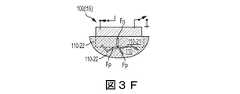
図2は、過渡電子デバイス100(図1に示す)に対する分解事象をトリガするための一般化された方法を示す流れ図であり、図3A、図3B、図3C、図3D、図3Eおよび図3Fは、例示的な分解事象の前および間における過渡電子デバイス100の一部を示す部分側断面図である。 FIG. 2 is a flow diagram illustrating a generalized method for triggering a decomposition event for a transient electronic device 100 (shown in FIG. 1), FIG. 3A, FIG. 3B, FIG. 3C, FIG. 3D, FIG. 3E and FIG. 3F. Is a partial side sectional view showing a part of the transient
図2の上部を参照すると、過渡電子デバイス100(t0)(図1)は通常動作を受ける(すなわち、機能回路120が意図したとおりに動作する)。図3Aは、デバイス100(t0)の一部を示す簡略断面図であり、自己制限抵抗素子140の抵抗部142は、局所的な領域110−21の上で脆弱ガラス基板110の上面111上に配置された金属構造として示されており、電流制御部145は、閉(すなわち、導通)状態のスイッチとして示されている。この時間t0において、スイッチ部150は開いている(すなわち、非導通状態にある)ため、バッテリPSから自己制限抵抗素子140を通って電流は流れず、したがって、抵抗部142によって熱が発生しない。したがって、時間t0において、局所的な領域110−21における局所的な温度TLRは、脆弱ガラス基板110の周囲の隣接領域110−22と同じ(相対的に低い)初期温度T0をとる。Referring to the upper part of FIG. 2, the transient electronic device 100 (t0) (FIG. 1) undergoes normal operation (that is, the
図2の上部付近のブロック205を参照すると、時間t10において、たとえば、トリガ事象信号が(たとえば、無線で送信された光またはRF信号に応答して)センサによって検出されたとき、または、不正な改ざんが検出されたとき、過渡事象が開始される。 Referring to block 205 near the top of FIG. 2, at time t10, for example, when a trigger event signal is detected by a sensor (eg, in response to a light or RF signal transmitted wirelessly), or is incorrect. When tampering is detected, a transient event is initiated.
ブロック210(図2および図3B)に示すように、時間t11(すなわち、時間t10後の瞬間)において、トリガ信号TS(図1)がアサートされ、スイッチ素子150の制御端子に印加され、それによって、スイッチ150が作動して、抵抗部142および電流制御部145を通るトリガ電流ITの流れが開始し、それにより、抵抗部142が脆弱ガラス基板110の上面111を通じて局所的な領域110−21に伝達される熱HGを発生させ始め、それによって、局所的な温度TLRが初期温度T0を上回って増大させられる。As shown in block 210 (FIGS. 2 and 3B), at time t11 (ie, the moment after time t10), the trigger signal TS (FIG. 1) is asserted and applied to the control terminal of the
ブロック220(図2および図3C)に示すように、その後の時間t12において、トリガ電流ITの継続的な流れにより、抵抗部142は、局所的な温度TLRを所定の目標温度T1に向けて急速に増大させる測度において熱HGを発生させられる。本発明の一態様によれば、この急速な温度増大は、周囲領域110−22における温度よりも速い速度において、局所的な温度TLRを増大させる速度で生じる。すなわち、図3Cに示すように、自己制限抵抗素子140から発生した熱HGは、放散する熱HGが局所的な領域110−21を出て周囲領域110−22に入るよりも速い速度で局所的な領域110−21に入り、それによって、局所的な領域110−21の局所的な温度TLRを初期温度T0からより高い目標(第1)温度レベルT1に向かって急速に増大させ、一方で周囲領域110−22を実質的により低い温度に維持する。As shown in block 220 (FIGS. 2 and 3C), in the subsequent time t12, the continued flow of trigger currentI T, resistor 142, the local temperatureT LR to a predetermined target temperaturesT 1 It is caused to generate heat HG in rapid measures to increase toward. According to one aspect of the present invention, the rapid temperature increase in the speed higher than the temperature in the surrounding area 110-22, occurs at a rate that increases the local temperature TLR. That is, as shown in FIG. 3C, the heatH G generated from the self-limiting
ブロック230(図2および図3D)に示すように、電流制限部145は、時間t13において、抵抗部142を通るトリガ電流の流れを終結させる開回路条件を生成することによって熱HGの生成を終結させるように作動する。本発明の別の態様によれば、発生した熱の終結が、局所的な領域110−21から熱HDをより低温の周囲領域110−22へと放散させることによって、局所的な温度TLRをより低い(第2の)温度T2に向かって急速に低減させるように、自己制限抵抗素子が構成される。
ブロック240(図2および図3E)に示すように、時間t14において、図3Cおよび図3Dを参照して上述した急速な温度増大および急速な温度低下によって生成された熱パルスは、脆弱ガラス基板110の局所的な領域110−21内に、局所的な領域110−21に初期破砕力F0を生成するのに十分な応力プロファイルを生成する。As shown in block 240 (FIGS. 2 and 3E), at time t14, the thermal pulses generated by the rapid temperature increase and decrease described above with reference to FIGS. 3C and 3D are the
ブロック240(図2および図3E)に示すように、時間t14において、図3Cおよび図3Dを参照して上述した急速な温度増大および急速な温度低下によって生成された熱パルスは、脆弱ガラス基板110の局所的な領域110−21内に、局所的な領域110−21に初期破砕力F0を生成するのに十分な力を有する応力プロファイルを生成する。その後、ブロック250(図2および図3F)に示すように、時間t15において、初期破砕力F0は、局所的な領域110−21から脆弱ガラス基板110および電子素子122全体を通じて放射する伝播破砕力FPを生成し、それによって、図1の下部におけるデバイス100(t2)によって示されている完全な分解が引き起こされる。したがって、上述したように脆弱ガラス基板110に熱パルスを発生するようにトリガ機構130を構成すること、および、熱パルスが加えられたことに応答して局所的な領域110−21に初期破砕力F0を発生するように、かつ、初期破砕力F0が、上述したように脆弱ガラス基板110および電子素子122を完全に分解させる伝播破砕力FPを引き起こすように、脆弱ガラス基板110を構成することによって、本発明は、パルス整形回路および複雑なアドレス指定構成を必要とせずに、低コスト、高信頼性の過渡電子デバイス100の構築を容易にする。As shown in block 240 (FIGS. 2 and 3E), at time t14, the thermal pulses generated by the rapid temperature increase and decrease described above with reference to FIGS. 3C and 3D are the
図4は、図3A〜図3Fを参照して上述した例示的な分解事象の間に自己制限抵抗素子140によって生成される例示的な熱パルスを示す局所的な温度TLRの変化を示す時間−温度グラフである。図5は、例示的な分解事象中の自己制限抵抗素子140の例示的な動作特性を示す時間−電圧/電流グラフである。図4に示すように、局所的な温度TLRは、時間t11まで(すなわち、図3Bを参照して上述したようにトリガ電流の流れが開始されるまで)初期温度T0(たとえば約140℃)にとどまる。時刻t11から時刻t13までの期間中のその後の急速な増大は、図3Bおよび図3Cを参照して上述したように、発生した熱HGが局所的な領域110−21に入ることによって引き起こされる。自己制限抵抗素子140は、時間t13で生じる、局所的な温度TLRのピーク(最高)値(すなわち、図4の図示の例では約220℃である高い/第1の温度T1)が、脆弱ガラス基板110を形成するガラスの融点温度TMPよりも高くなるように構成されている。自己制限抵抗素子140が作動した後、図3Dに示すように、局所的な領域110−21から脆弱ガラス基板110の周囲領域110−22に熱が発散し始め、その後の時間t13〜t14の期間中の急速な温度低減(たとえば、図4に示す例では、約1秒で約220℃から約200℃への約20℃)を引き起こす。時間t14において、温度T1への急速な増大、および、それに続く急速な冷却の期間に起因する応力プロファイルは、図3Eに示すように、局所的な領域110−21において初期破砕力F0を生じる。時刻t14のほぼ直後には、初期破砕力F0が伝播破砕力FPを引き起こし、これは、図3Fに示すように、デバイス100を非常に短い時間で完全に分解し、急速な冷却をもたらす。図5に示すように、自己制限抵抗素子140を流れる電流は、スイッチ150が作動する時刻t10で最大値(たとえば、約5アンペア)にジャンプし、抵抗部142が徐々に加熱するとゆっくりと低減し、次いで電流制御素子145が作動する時間t14でゼロになる。対照的に、自己制限抵抗素子140にわたる電圧は、抵抗部142が徐々に加熱するときに、時間t10において0Vから中間値(たとえば、約4ボルト)へと徐々に増大し、次いで、電流制御素子145が作動する時間t14において最大値(たとえば、約9ボルト)にジャンプする。FIG. 4 shows a change inlocal temperature TLR showing an exemplary thermal pulse generated by the self-limited
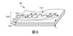
図6は、対向する(第1および第2の)端子142A−1/2にそれぞれ接続され、上述のように局所的な領域110−21の上に配置されている2つの(第1および第2の)抵抗構造(抵抗部)142A−1と142A−2との間に直列に接続されたヒューズ型電流制限部145Aを備える自己制限抵抗素子140Aを有する過渡電子デバイス100Aの一部を示す斜視図である。図1に示す実施形態の場合と同様に、ともに動作可能に接続されると、端子141A−1はスイッチ素子(図示せず)によって直流(DC)電源に接続され、端子141A−2は適切な接地構造に接続される。好ましい実施形態では、抵抗構造142A−1および142A−2ならびにヒューズ型電流制限部145Aは、単一の(共通の)抵抗材料(たとえば、マグネシウム、銅、タングステン、アルミニウム、モリブデンおよびクロムのうちの1つまたは複数)を脆弱ガラス基板110Aの上面111A上に直接堆積させることによって生成される。抵抗材料の選択に関連する重要な問題は、それが十分に導電性であり、熱パルスの急速加熱プロセス中に抵抗部142A−1および142A−2ならびに電流制限部145Aによって生成される熱が効率的に局所的な領域110−21へと伝達されるのに十分に、脆弱ガラス基板110Aの上面111Aに付着することである。抵抗構造142A−1および142A−2がそれぞれ相対的に大きな構造142A−1/2を含むように、抵抗材料が印刷、エッチングまたは他の方法でパターニングされ、ヒューズ型電流制限部145Aは、ヒューズ素子として機能するように構成されている相対的に細く薄い構造を備える。すなわち、端子141A−1と141A−2との間に十分に大きな電流が流れると、抵抗構造142A−1および142A−2ならびに電流制限部145Aは抵抗加熱を受けるが、その断面が相対的に細いため、電流制限部145Aはより高い温度を生成することになり、この温度は好ましい実施形態では、適切なトリガ電流にさらされたときに溶融および破断を引き起こすのに十分である。自己制限抵抗素子の電流制御部を実装するためにヒューズ型電流制限部(ヒューズ素子)を使用して電流制限部145Aを実装することによって、熱パルスの急速加熱プロセスの間に自己制限抵抗素子140Aによって発生する熱量を独立して制御するための低コスト、単純で信頼性の高い構造が提供され、熱パルスの急速冷却部分の開始時に抵抗構造142A−1および142A−2を通るトリガ電流の流れを終結させる開回路状態(すなわち、溶融/破断による)が確実に生成される。 FIG. 6 shows two (first and first) terminals connected to opposite (first and second)
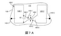
図7Aおよび図7Bは、脆弱ガラス基板110Bの上面111B上に直接配置されたボウタイ型パターン化金属層構造を含む自己制限抵抗素子140B−1および140B−2を示す平面図であり、各抵抗素子は、2つの抵抗構造の下向きテーパ部分の間に接続されたヒューズ素子を含む。たとえば、自己制限抵抗素子140B−1は、下向きテーパ部分146B−11を含む第1の抵抗構造142B−11と、下向きテーパ部分146B−12を含む第2の抵抗構造142B−12と、それぞれ下向きテーパ部分146B−11のテーパ端部147B−11と下向きテーパ部分146B−12のテーパ端部147B−12との間に接続されたヒューズ素子145B−1とを含む。同様に、自己制限抵抗素子140B−2は、下向きテーパ部分146B−21を含む第1の抵抗構造142B−21と、下向きテーパ部分146B−22を含む第2の抵抗構造142B−22と、テーパ端部147B−21とテーパ端部147B−22との間に接続されたヒューズ素子145B−2とを含む。各事例において、ヒューズ素子145B−1および145B−2は、トリガ電流にさらされたときに溶融し破断するように構成された幅W1を有する細い頸部構造を含む。好ましい実施形態では、幅W1は、脆弱ガラス基板110Bの厚さ(たとえば、図6に示す厚さT)よりも大きい。たとえば、厚さ0.25mmの脆弱ガラス基板を使用する実際的な実施形態では、ヒューズ素子145B−1および145B−2は、少なくとも0.3mmの幅W1を有する。対照的に、より大きな抵抗は電源からより多くの電力およびエネルギーを必要とするが、両方の自己制限抵抗素子(たとえば抵抗構造146B−11)の抵抗構造はほぼ任意の幅(サイズ)W2を有することができる。 7A and 7B are plan views showing self-restricting
図7Aおよび図7Bに示される代替的な実施形態によって示されるように、異なるヒューズ構成を利用して所望の熱パルス特性を生成することができる。具体的には、ヒューズ素子145B−1が、テーパ端部147B−11と147B−12との間に延伸する直線状の矩形構造を含み、ヒューズ素子145B−2が、テーパ状の端部147B−21と147B−22との間に延伸するS字形状を有している点で、自己制限抵抗素子140B−1と140B−2とは異なっている。これらの異なるヒューズ構成は、トリガの抵抗を調整すること、および、破砕までの時間に影響を与え得る、熱が加えられる面積を調整することにより、加えられるエネルギーおよび電力を制御することを可能にすることによって、異なる利益をもたらす。 Different fuse configurations can be utilized to generate the desired thermal pulse characteristics, as shown by the alternative embodiments shown in FIGS. 7A and 7B. Specifically, the
図8は、送信波信号WS(たとえば、光波信号、無線周波数(RF)、または音響/音声信号)を検出するように構成されており、次いで、スイッチ素子を作動させるために使用される電子トリガ信号TSを生成するように構成されているセンサ160Cを含む遠隔(無線)制御可能トリガ機構130Cを含む部分過渡電子デバイス100Cを示す回路図である。前述の実施形態と同様に、トリガ機構130Cは、自己制限抵抗素子140Cとスイッチ素子150Cとを含み、自己制限抵抗素子140Cは、第1の抵抗構造142C−1と第2の抵抗構造142C−2との間に接続されたヒューズ素子145Cを含む。例示的な実施形態では、スイッチ素子150Cは、シリコン制御整流器を用いて実現され、波信号WSは光信号であり、センサ160Cは、スイッチ素子150Cに動作可能に結合され、光信号WSに応答して作動するように構成されているフォトダイオード(または他の光波センサ)であり、それによって、フォトダイオード160Cを流れる電流が、電流を利用してシリコン制御整流器をラッチさせることによってスイッチ素子150Cを作動させ、次にバッテリPSが自己制限抵抗素子140Cにわたって結合され、最終的に、ガラス基板および任意の含まれている電子装置が上述したように分解(破砕)される。この実施例では、光信号を使用して過渡電子デバイスの遠隔作動が達成されているが、RF信号および音波信号が、フォトダイオード160Cを無線周波センサまたは音響波センサに置き換えることによって利用されてもよい。さらに、破砕シーケンスを開始するために、他の物理的および化学的刺激もまた、適切なセンサと組み合わせて利用されてもよい。同様に、この実際的な実施形態においてはシリコン制御整流器150Cを使用してラッチが達成されているが、単一MOSFETトランジスタまたはMOSFETベース多素子回路を含むラッチ回路のような他のスイッチ素子も利用されてもよい。 FIG. 8 is configured to detect a transmitted wave signal WS (eg, a light wave signal, a radio frequency (RF), or an acoustic / audio signal) and then an electronic trigger used to activate the switch element. FIG. 6 is a circuit diagram illustrating a partially transient
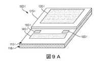
図9Aおよび図9Bは、センサおよび/またはスイッチ素子が「ホスト」脆弱ガラス基板上に直接的に製造もしくは搭載されているか、または、半導体層上の電子素子と同時に作製されているかのいずれかである、代替の実際的な実施形態による簡略化された過渡電子デバイス100D−1および100D−2を示す。たとえば、図9Aは、センサ160D−1(たとえば、フォトダイオード)およびスイッチ素子150D−1(たとえば、シリコン制御整流器)が、脆弱ガラス基板110Dの表面111D上に直接的に印刷またはパターン化された適切な材料によって実装されるデバイス110D−1を示す。代替的に、図9Bに示すように、デバイス110D−2は、電子素子122Dが形成される半導体構造121D−2(たとえば、ICチップまたはSOI層)に対してCMOS作製技法を使用して作製されたセンサ160D−2およびスイッチ素子150D−2を含む。両方の実施形態において、自己制限抵抗素子140D−1および140D−2が基板1上に直接形成される。別の実施形態(図示せず)では、センサおよびスイッチ素子の一方または両方がホストPC基板上に配置され、適切な導電性接続によって接続されてもよい。 9A and 9B show either the sensor and / or the switch element is either manufactured or mounted directly on the "host" fragile glass substrate or simultaneously manufactured with the electronic device on the semiconductor layer. Some simplified transient
Claims (10)
Translated fromJapanese脆弱ガラス基板と、
1つまたは複数の電子素子であって、前記脆弱ガラス基板の分解が前記電子素子の分解を引き起こすように、前記脆弱ガラス基板上に配置されている、1つまたは複数の電子素子と、
トリガ機構であり、
前記脆弱ガラス基板の局所的な領域上に配置された抵抗材料から成る自己制限抵抗素子と、
前記自己制限抵抗素子に結合されたスイッチ素子と
を備え、
前記自己制限抵抗素子は、前記スイッチ素子が作動して電源から前記自己制限抵抗素子を通るトリガ電流を開始した後の第1の期間中に、前記自己制限抵抗素子が発生させる熱が、前記局所的な領域の局所的な温度を初期温度から第1の温度レベルに向かって急速に上昇させるように構成されており、
前記自己制限抵抗素子の電流制限部が、前記局所的な領域の前記局所的な温度が前記第1の温度レベルに達したときに前記トリガ電流の流れを終結させ、それにより前記局所的な温度を前記第1の温度レベルから第2の温度レベルまで急速に低下させるように、前記トリガ電流の流れを独立に制御する、トリガ機構と
を備え、
前記脆弱ガラス基板は前記局所的な温度の急速な上昇と前記局所的な温度の急速な低下とを含む熱パルスによって前記局所的な領域内に生成される応力プロファイルが、前記局所的な領域に初期破砕力を発生させるのに十分であるように構成されている、過渡電子デバイス。It ’s a transient electronic device,
With a fragile glass substrate,
One or more electronic devices, one or more electronic devices arranged on the fragile glass substrate such that decomposition of the fragile glass substrate causes decomposition of the electronic device.
It is a trigger mechanism
A self-limited resistor element made of a resistance material placed on a local region of the fragile glass substrate,
A switch element coupled to the self-limit resistance element is provided.
In the self-restricting resistance element, the heat generated by the self-restricting resistance element is generated locally during the first period after the switch element is activated and the trigger current through the self-restricting resistance element is started from the power source. It is configured to rapidly increase the local temperature of the region from the initial temperature towards the first temperature level.
The current limiting portion of the self-restricting resistor element terminates the flow of the trigger current when the local temperature in the local region reaches the first temperature level, thereby causing the local temperature. Equipped with a trigger mechanism that independently controls the flow of the trigger current so that the temperature drops rapidly from the first temperature level to the second temperature level.
The stress profile brittle glass substrates that are generated on the local region by the heat pulse and a rapid decreasein the rapid risein thelocal temperature thelocal temperature is, the local area A transient electronic device that is configured to be sufficient to generate an initial crushing force.
前記第1の端子は前記スイッチ素子によって直流(DC)電源に接続されており、
前記第2の端子は接地に接続されている、
請求項1に記載の過渡電子デバイス。The self-limited resistance element includes at least one resistance unit connected in series with the current limiting unit between the first terminal and the second terminal.
The first terminal is connected to a direct current (DC) power supply by the switch element.
The second terminal is connected to ground.
The transient electronic device according to claim 1.
前記電流制限部は、前記第1の抵抗構造と前記第2の抵抗構造との間に接続されており、前記第1の期間後に破断し、破断によって、前記第1の抵抗構造および前記第2の抵抗構造を通る前記トリガ電流の流れを終結させるように構成されているヒューズ素子を含む、
請求項3に記載の過渡電子デバイス。The at least one resistance portion includes a first resistance structure and a second resistance structure.
The current limiting portion is connected between the first resistance structure and the second resistance structure, and breaks after the first period, and by the break, the first resistance structure and the second resistance structure are broken. Includes a fuse element configured to terminate the flow of said trigger current through the resistance structure of the.
The transient electronic device according to claim 3.
電源と自己制限抵抗素子との間に結合されているスイッチ素子を、前記電源から前記スイッチ素子および前記自己制限抵抗素子を通じて直流電流が流れるように作動させることにより、前記脆弱ガラス基板の局所的な領域に急速な熱増大を生じさせるステップであって、前記直流電流によって、前記局所的な領域の局所的な温度を初期温度から第1の温度まで急速に上昇させるのに十分高い速度で、前記自己制限抵抗素子に、熱を発生させて前記局所的な領域へと伝達させ、前記第1の温度は前記融点温度より高い、急速な熱増大を生じさせるステップと、
前記局所的な領域内の前記局所的な温度が前記第1の温度から第2の温度まで急速に低減するように、急速な熱低減を生じさせるステップであって、前記第2の温度は前記第1の温度よりも低い、急速な熱低減を生じさせるステップと
を含み、
前記急速な熱増大および前記急速な熱低減によって発生する熱パルスは、前記局所的な領域内で初期破砕力を生成し、前記急速な熱増大の持続時間は、前記自己制限抵抗素子によって独立して制御される、方法。It is basically a trigger method for starting pulverization of an electronic element arranged on a fragile glass substrate made of glass having a certain melting point temperature.
By operating the switch element coupled between the power supply and the self-restricting resistance element so that a direct current flows from the power source through the switch element and the self-restricting resistance element, the fragile glass substrate is localized. The step of causing a rapid thermal increase in the region, said at a rate high enough to allow the direct current to rapidly raise the local temperature of the local region from the initial temperature to the first temperature. A step of causing a self-restricting resistance element to generate heat and transfer it to the local region, the first temperature being higher than the melting point temperature, and causing a rapid heat increase.
A step of causing a rapid heat reduction such that the local temperature in the local region rapidly decreases from the first temperature to the second temperature, wherein the second temperature is said. Including steps that result in rapid heat reduction below the first temperature.
The thermal pulses generated by the rapid heat increase and the rapid heat reduction generate an initial crushing force within the local region, and the duration of the rapid heat increase is independent of the self-limiting resistance element. Controlled, method.
脆弱ガラス基板と、
前記脆弱ガラス基板上に配置された1つまたは複数の電子素子と、
トリガ機構であり、
前記脆弱ガラス基板上に配置された第1の抵抗構造体と第2の抵抗構造体との間に配置されたヒューズ素子を含む自己制限抵抗素子と、
スイッチ素子であって、前記自己制限抵抗素子と電源との間に、前記スイッチ素子の作動が前記電源から前記自己制限抵抗素子を通るトリガ電流を開始させるように結合されている前記スイッチ素子と
を備える、トリガ機構と
を備え、
前記自己制限抵抗素子は、前記トリガ電流を前記電源から前記自己制限抵抗素子に流すことにより、前記脆弱ガラス基板内に熱パルスが生成されるように構成されており、
前記脆弱ガラス基板は、前記熱パルスによって生成される応力プロファイルが、前記脆弱ガラス基板の局所的な領域内の初期破砕力を引き起こすように構成されており、前記脆弱ガラス基板は、前記初期破砕力が、前記脆弱ガラス基板および前記1つまたは複数の電子素子の完全な分解をもたらす伝搬破砕力を引き起こすようにさらに構成されている、過渡電子デバイス。It ’s a transient electronic device,
With a fragile glass substrate,
With one or more electronic devices arranged on the fragile glass substrate,
It is a trigger mechanism
A self-limiting resistance element including a fuse element arranged between the first resistance structure and the second resistance structure arranged on the fragile glass substrate.
A switching element, between the self-limiting resistive element and the power source, andsaid switching element operation of the switching element is coupled to initiate a trigger current through the self-limiting resistor element from said power source Equipped with a trigger mechanism
The self-limiting resistance element is configured to generate a heat pulse in the fragile glass substrate by passing the trigger current from the power source to the self-limiting resistance element.
The fragile glass substrate is configured such that the stress profile generated by the thermal pulse causes an initial crushing force within a local region of the fragile glass substrate, and the fragile glass substrate has the initial crushing force. Is a transient electronic device further configured to cause a propagating crushing force that results in the complete decomposition of the fragile glass substrate and the one or more electronic devices.
Applications Claiming Priority (2)
| Application Number | Priority Date | Filing Date | Title |
|---|---|---|---|
| US15/220,164US10026579B2 (en) | 2016-07-26 | 2016-07-26 | Self-limiting electrical triggering for initiating fracture of frangible glass |
| US15/220,164 | 2016-07-26 |
Publications (2)
| Publication Number | Publication Date |
|---|---|
| JP2018019078A JP2018019078A (en) | 2018-02-01 |
| JP6970543B2true JP6970543B2 (en) | 2021-11-24 |
Family
ID=59592817
Family Applications (1)
| Application Number | Title | Priority Date | Filing Date |
|---|---|---|---|
| JP2017134450AExpired - Fee RelatedJP6970543B2 (en) | 2016-07-26 | 2017-07-10 | Self-limited electrical trigger to start breaking fragile glass |
Country Status (3)
| Country | Link |
|---|---|
| US (3) | US10026579B2 (en) |
| EP (1) | EP3276831B1 (en) |
| JP (1) | JP6970543B2 (en) |
Families Citing this family (16)
| Publication number | Priority date | Publication date | Assignee | Title |
|---|---|---|---|---|
| US9154138B2 (en) | 2013-10-11 | 2015-10-06 | Palo Alto Research Center Incorporated | Stressed substrates for transient electronic systems |
| US9780044B2 (en) | 2015-04-23 | 2017-10-03 | Palo Alto Research Center Incorporated | Transient electronic device with ion-exchanged glass treated interposer |
| US10012250B2 (en) | 2016-04-06 | 2018-07-03 | Palo Alto Research Center Incorporated | Stress-engineered frangible structures |
| US10026579B2 (en) | 2016-07-26 | 2018-07-17 | Palo Alto Research Center Incorporated | Self-limiting electrical triggering for initiating fracture of frangible glass |
| US10224297B2 (en) | 2016-07-26 | 2019-03-05 | Palo Alto Research Center Incorporated | Sensor and heater for stimulus-initiated fracture of a substrate |
| WO2018069780A1 (en)* | 2016-10-11 | 2018-04-19 | King Abdullah University Of Science And Technology | Activatable electronic component destruction device |
| US10903173B2 (en) | 2016-10-20 | 2021-01-26 | Palo Alto Research Center Incorporated | Pre-conditioned substrate |
| US10626048B2 (en) | 2017-12-18 | 2020-04-21 | Palo Alto Research Center Incorporated | Dissolvable sealant for masking glass in high temperature ion exchange baths |
| DE102018107143A1 (en)* | 2018-03-26 | 2019-09-26 | Volkswagen Ag | Vehicle window and method for its manufacture |
| US10717669B2 (en) | 2018-05-16 | 2020-07-21 | Palo Alto Research Center Incorporated | Apparatus and method for creating crack initiation sites in a self-fracturing frangible member |
| US11107645B2 (en) | 2018-11-29 | 2021-08-31 | Palo Alto Research Center Incorporated | Functionality change based on stress-engineered components |
| US10947150B2 (en) | 2018-12-03 | 2021-03-16 | Palo Alto Research Center Incorporated | Decoy security based on stress-engineered substrates |
| US10969205B2 (en) | 2019-05-03 | 2021-04-06 | Palo Alto Research Center Incorporated | Electrically-activated pressure vessels for fracturing frangible structures |
| US20200373109A1 (en)* | 2019-05-21 | 2020-11-26 | Rosemount Aerospace, Inc. | Fuse assembly and method of making |
| US11904986B2 (en) | 2020-12-21 | 2024-02-20 | Xerox Corporation | Mechanical triggers and triggering methods for self-destructing frangible structures and sealed vessels |
| US12013043B2 (en) | 2020-12-21 | 2024-06-18 | Xerox Corporation | Triggerable mechanisms and fragment containment arrangements for self-destructing frangible structures and sealed vessels |
Family Cites Families (93)
| Publication number | Priority date | Publication date | Assignee | Title |
|---|---|---|---|---|
| US2529210A (en) | 1947-05-23 | 1950-11-07 | Joseph F Butler | Cutting apparatus for wallboards and the like |
| GB1138401A (en) | 1965-05-06 | 1969-01-01 | Mallory & Co Inc P R | Bonding |
| US3601114A (en) | 1969-01-21 | 1971-08-24 | Norton Co | Method and apparatus for cutting complex shapes |
| US3673667A (en) | 1970-11-23 | 1972-07-04 | Whittaker Corp | Method for producing complex shapes by filled billet extrusion |
| US3666967A (en) | 1971-05-12 | 1972-05-30 | Us Navy | Self-destruct aluminum-tungstic oxide films |
| US3882323A (en) | 1973-12-17 | 1975-05-06 | Us Navy | Method and apparatus for protecting sensitive information contained in thin-film microelectonic circuitry |
| US4102664A (en) | 1977-05-18 | 1978-07-25 | Corning Glass Works | Method for making glass articles with defect-free surfaces |
| US4139359A (en) | 1977-11-02 | 1979-02-13 | Ppg Industries, Inc. | Method and apparatus for shaping glass sheets by roll forming |
| DE3230554C2 (en) | 1982-04-28 | 1984-07-26 | GTI Glastechnische Industrie Peter Lisec, GmbH, Amstetten | Method and device for cutting laminated glass |
| SE435352B (en) | 1983-05-04 | 1984-09-24 | Hydro Betong Ab | CONSTRUCTION BODY FOR A PREPARED CONSTRUCTION CONSISTING OF A NUMBER WITH OTHER COMBINED PLASTICS OF PLASTIC MATERIAL, OF EXV URETANCUM AND SET TO MAKE SAID BODY |
| GB8322258D0 (en) | 1983-08-18 | 1983-09-21 | Holmes A | Security and protection screens |
| US4558622A (en) | 1983-11-04 | 1985-12-17 | Russell Tausheck | Apparatus for cutting laminated glass |
| US4739555A (en) | 1985-06-18 | 1988-04-26 | Werner Jurgens | Laminated glass cutter |
| DE69031627T2 (en) | 1989-12-22 | 1998-03-05 | Perkins | INTEGRATED DATA COMMUNICATION SYSTEM |
| FR2681472B1 (en) | 1991-09-18 | 1993-10-29 | Commissariat Energie Atomique | PROCESS FOR PRODUCING THIN FILMS OF SEMICONDUCTOR MATERIAL. |
| GB9201863D0 (en) | 1992-01-29 | 1992-03-18 | Dunn Kenneth R | Multi glazing air cushion release unit |
| US5791056A (en) | 1996-11-22 | 1998-08-11 | Messina; Gary D. | Emergency glass breaking tool |
| DE19958750B4 (en) | 1999-12-07 | 2006-08-24 | Robert Bosch Gmbh | Leaky wave antenna |
| KR100771258B1 (en) | 2000-05-09 | 2007-10-29 | 가부시키가이샤 한도오따이 에네루기 켄큐쇼 | Identity verification system, identity verification method and mobile phone device |
| FR2823599B1 (en) | 2001-04-13 | 2004-12-17 | Commissariat Energie Atomique | DEMOMTABLE SUBSTRATE WITH CONTROLLED MECHANICAL HOLDING AND METHOD OF MAKING |
| GB0127083D0 (en) | 2001-11-10 | 2002-01-02 | P W Allen & Company Ltd | Device for breaking glass |
| FR2837304B1 (en)* | 2002-03-13 | 2004-05-28 | Commissariat Energie Atomique | SECURE ELECTRONIC DEVICE |
| US20040031966A1 (en) | 2002-08-16 | 2004-02-19 | Forrest Stephen R. | Organic photonic integrated circuit using a photodetector and a transparent organic light emitting device |
| JP2004075504A (en) | 2002-08-22 | 2004-03-11 | Nippon Sheet Glass Co Ltd | Method and apparatus for multiply bending glass sheet |
| DE10305733B4 (en) | 2003-02-12 | 2005-10-20 | Saint Gobain Sekurit D Gmbh | Method of producing predetermined breaking points in glass panes, glass pane with weakening zone and use of same |
| JP4115859B2 (en) | 2003-02-28 | 2008-07-09 | 株式会社日立製作所 | Anodic bonding method and electronic device |
| DE10309826B4 (en) | 2003-03-05 | 2009-11-12 | Schott Ag | Process for structuring phosphate glasses by non-destructive ion exchange, structured phosphate glasses and their use |
| US7002517B2 (en) | 2003-06-20 | 2006-02-21 | Anritsu Company | Fixed-frequency beam-steerable leaky-wave microstrip antenna |
| EP1517073A1 (en) | 2003-09-19 | 2005-03-23 | Universita degli Studi di Trento | ESP glass rupture disk |
| JP2007509315A (en) | 2003-10-09 | 2007-04-12 | オカス コーポレーション | Two-layer bolometer-type infrared sensor and method for manufacturing the same |
| US20050082331A1 (en) | 2003-10-17 | 2005-04-21 | Chi-Hong Yang | Tempered glass breaker |
| DE102004015546B4 (en) | 2004-03-30 | 2011-05-12 | Infineon Technologies Ag | An integrated circuit semiconductor chip and method for securing a semiconductor integrated circuit |
| US20060270190A1 (en) | 2005-05-25 | 2006-11-30 | The Regents Of The University Of California | Method of transferring a thin crystalline semiconductor layer |
| WO2007019277A2 (en) | 2005-08-03 | 2007-02-15 | California Institute Of Technology | Method of forming semiconductor layers on handle substrates |
| US7880248B1 (en) | 2005-10-17 | 2011-02-01 | Teledyne Technologies Incorporated | Destructor integrated circuit chip, interposer electronic device and methods |
| KR101389808B1 (en) | 2005-11-18 | 2014-04-29 | 가부시키가이샤 한도오따이 에네루기 켄큐쇼 | Photoelectric conversion device |
| US8168050B2 (en) | 2006-07-05 | 2012-05-01 | Momentive Performance Materials Inc. | Electrode pattern for resistance heating element and wafer processing apparatus |
| GB0717489D0 (en) | 2007-09-08 | 2007-10-17 | Design Factor Ni The Ltd | A Glass breaking device |
| US7623560B2 (en) | 2007-09-27 | 2009-11-24 | Ostendo Technologies, Inc. | Quantum photonic imagers and methods of fabrication thereof |
| JP2009212315A (en) | 2008-03-04 | 2009-09-17 | Elpida Memory Inc | Semiconductor device and manufacturing method thereof |
| EP2300953B1 (en) | 2008-06-13 | 2013-01-23 | Nxp B.V. | Intrusion protection using stress changes |
| CN103043900A (en) | 2008-08-08 | 2013-04-17 | 康宁股份有限公司 | Strengthened glass articles and methods of making |
| JP2010045132A (en)* | 2008-08-11 | 2010-02-25 | Nec Electronics Corp | Electric fuse and semiconductor device |
| KR20100063269A (en) | 2008-12-03 | 2010-06-11 | 주식회사 동부하이텍 | Image sensor and method for manufacturing thereof |
| US8089285B2 (en) | 2009-03-03 | 2012-01-03 | International Business Machines Corporation | Implementing tamper resistant integrated circuit chips |
| US8130072B2 (en) | 2009-05-14 | 2012-03-06 | Palo Alto Research Center Incorporated | Vanadium oxide thermal microprobes |
| CN201532635U (en) | 2009-09-03 | 2010-07-21 | 百富计算机技术(深圳)有限公司 | A safety protection device |
| US8946590B2 (en) | 2009-11-30 | 2015-02-03 | Corning Incorporated | Methods for laser scribing and separating glass substrates |
| FR2953213B1 (en) | 2009-12-01 | 2013-03-29 | Saint Gobain | METHOD FOR ION ABRASION SURFACE STRUCTURING, STRUCTURED SURFACE AND USES |
| TWI438162B (en) | 2010-01-27 | 2014-05-21 | Wintek Corp | Cutting method and preparatory cutting structure for reinforced glass |
| US8393175B2 (en) | 2010-08-26 | 2013-03-12 | Corning Incorporated | Methods for extracting strengthened glass substrates from glass sheets |
| KR20130141527A (en) | 2010-10-15 | 2013-12-26 | 시리트 엘엘씨 | Surface scattering antennas |
| US8616024B2 (en) | 2010-11-30 | 2013-12-31 | Corning Incorporated | Methods for forming grooves and separating strengthened glass substrate sheets |
| US8607590B2 (en) | 2010-11-30 | 2013-12-17 | Corning Incorporated | Methods for separating glass articles from strengthened glass substrate sheets |
| US8539794B2 (en) | 2011-02-01 | 2013-09-24 | Corning Incorporated | Strengthened glass substrate sheets and methods for fabricating glass panels from glass substrate sheets |
| US20140300520A1 (en) | 2011-04-07 | 2014-10-09 | Polyvalor, Limited Partnership | Full-space scanning end-switched crlh leaky-wave antenna |
| US8635887B2 (en) | 2011-08-10 | 2014-01-28 | Corning Incorporated | Methods for separating glass substrate sheets by laser-formed grooves |
| TWI415809B (en) | 2011-08-12 | 2013-11-21 | Wintek Corp | Reinforced glass cell and method for fabricating the same and cover glass having the reinforced glass cell |
| US20130082383A1 (en) | 2011-10-03 | 2013-04-04 | Texas Instruments Incorporated | Electronic assembly having mixed interface including tsv die |
| KR101979354B1 (en) | 2011-12-01 | 2019-08-29 | 더 보오드 오브 트러스티스 오브 더 유니버시티 오브 일리노이즈 | Transient devices designed to undergo programmable transformations |
| US9491700B2 (en)* | 2012-02-10 | 2016-11-08 | Lg Electronics Inc. | Method by which stations operating in power save mode in wireless LAN systems transmit and receive frames, and apparatus for supporting same |
| CN102617023B (en) | 2012-03-31 | 2014-12-31 | 洛阳兰迪玻璃机器股份有限公司 | Machining device for columnar curved toughened glass |
| CN102617022B (en) | 2012-03-31 | 2014-10-22 | 洛阳兰迪玻璃机器股份有限公司 | Machining method for columnar curved toughened glass |
| SE537874C2 (en) | 2012-04-13 | 2015-11-03 | Silex Microsystems Ab | CTE-adapted interposer and method of manufacturing one |
| US20130273717A1 (en) | 2012-04-17 | 2013-10-17 | Taiwan Semiconductor Manufacturing Co., Ltd. | Apparatus and Method for the Singulation of a Semiconductor Wafer |
| US9938180B2 (en) | 2012-06-05 | 2018-04-10 | Corning Incorporated | Methods of cutting glass using a laser |
| KR101395054B1 (en) | 2012-08-08 | 2014-05-14 | 삼성코닝정밀소재 주식회사 | Cutting method and stage for cutting of tempered glass |
| US8765536B2 (en) | 2012-09-28 | 2014-07-01 | International Business Machines Corporation | Stress engineered multi-layers for integration of CMOS and Si nanophotonics |
| US8816717B2 (en) | 2012-10-17 | 2014-08-26 | International Business Machines Corporation | Reactive material for integrated circuit tamper detection and response |
| US9385435B2 (en) | 2013-03-15 | 2016-07-05 | The Invention Science Fund I, Llc | Surface scattering antenna improvements |
| EP2984910B1 (en)* | 2013-04-12 | 2020-01-01 | The Board of Trustees of the University of Illionis | Inorganic and organic transient electronic devices |
| US9041205B2 (en) | 2013-06-28 | 2015-05-26 | Intel Corporation | Reliable microstrip routing for electronics components |
| JP5582232B1 (en) | 2013-07-30 | 2014-09-03 | 日本電気硝子株式会社 | Method for producing glass plate having curved shape, glass plate having curved shape, and apparatus for producing glass plate having curved shape |
| US9790128B2 (en) | 2013-08-07 | 2017-10-17 | Corning Incorporated | Laser controlled ion exchange process and glass articles formed therefrom |
| US9154138B2 (en)* | 2013-10-11 | 2015-10-06 | Palo Alto Research Center Incorporated | Stressed substrates for transient electronic systems |
| US9356603B2 (en) | 2013-10-11 | 2016-05-31 | Palo Alto Research Center Incorporated | Thermally tempered glass substrate using CTE mismatched layers and paste mixtures for transient electronic systems |
| US9294098B2 (en) | 2013-11-26 | 2016-03-22 | Lawrence Livermore National Security, Llc | System and method for on demand, vanishing, high performance electronic systems |
| US9850160B2 (en)* | 2013-12-17 | 2017-12-26 | Corning Incorporated | Laser cutting of display glass compositions |
| US9842812B2 (en)* | 2014-03-24 | 2017-12-12 | Honeywell International Inc. | Self-destructing chip |
| US9853361B2 (en) | 2014-05-02 | 2017-12-26 | The Invention Science Fund I Llc | Surface scattering antennas with lumped elements |
| US9711852B2 (en) | 2014-06-20 | 2017-07-18 | The Invention Science Fund I Llc | Modulation patterns for surface scattering antennas |
| US10381326B2 (en) | 2014-05-28 | 2019-08-13 | Invensas Corporation | Structure and method for integrated circuits packaging with increased density |
| FR3024136B1 (en) | 2014-07-24 | 2021-04-30 | Saint Gobain | PROCESS FOR BREAKING A SHEET OF GLASS |
| US9586857B2 (en) | 2014-11-17 | 2017-03-07 | International Business Machines Corporation | Controlling fragmentation of chemically strengthened glass |
| US9780044B2 (en) | 2015-04-23 | 2017-10-03 | Palo Alto Research Center Incorporated | Transient electronic device with ion-exchanged glass treated interposer |
| US9577047B2 (en) | 2015-07-10 | 2017-02-21 | Palo Alto Research Center Incorporated | Integration of semiconductor epilayers on non-native substrates |
| US10012250B2 (en) | 2016-04-06 | 2018-07-03 | Palo Alto Research Center Incorporated | Stress-engineered frangible structures |
| JP2017195257A (en)* | 2016-04-19 | 2017-10-26 | 富士通株式会社 | Self-destructive element, semiconductor device, electronic device, information protection system, and information protection method |
| US10026579B2 (en) | 2016-07-26 | 2018-07-17 | Palo Alto Research Center Incorporated | Self-limiting electrical triggering for initiating fracture of frangible glass |
| US10224297B2 (en) | 2016-07-26 | 2019-03-05 | Palo Alto Research Center Incorporated | Sensor and heater for stimulus-initiated fracture of a substrate |
| US10903173B2 (en) | 2016-10-20 | 2021-01-26 | Palo Alto Research Center Incorporated | Pre-conditioned substrate |
| US10026651B1 (en) | 2017-06-21 | 2018-07-17 | Palo Alto Research Center Incorporated | Singulation of ion-exchanged substrates |
| US10479300B2 (en) | 2017-10-06 | 2019-11-19 | Ford Global Technologies, Llc | Monitoring of vehicle window vibrations for voice-command recognition |
- 2016
- 2016-07-26USUS15/220,164patent/US10026579B2/enactiveActive
- 2017
- 2017-07-10JPJP2017134450Apatent/JP6970543B2/ennot_activeExpired - Fee Related
- 2017-07-24EPEP17182802.3Apatent/EP3276831B1/enactiveActive
- 2018
- 2018-07-12USUS16/033,783patent/US10332717B2/enactiveActive
- 2019
- 2019-06-06USUS16/433,603patent/US10950406B2/enactiveActive
Also Published As
| Publication number | Publication date |
|---|---|
| US10950406B2 (en) | 2021-03-16 |
| US10026579B2 (en) | 2018-07-17 |
| US20180033577A1 (en) | 2018-02-01 |
| US10332717B2 (en) | 2019-06-25 |
| JP2018019078A (en) | 2018-02-01 |
| US20180330907A1 (en) | 2018-11-15 |
| US20190311872A1 (en) | 2019-10-10 |
| EP3276831A1 (en) | 2018-01-31 |
| EP3276831B1 (en) | 2020-06-24 |
Similar Documents
| Publication | Publication Date | Title |
|---|---|---|
| JP6970543B2 (en) | Self-limited electrical trigger to start breaking fragile glass | |
| US11810871B2 (en) | Pre-conditioned self-destructing substrate | |
| JP6533757B2 (en) | Transient electronic devices with ion-exchanged glass-processed interposers | |
| US9356603B2 (en) | Thermally tempered glass substrate using CTE mismatched layers and paste mixtures for transient electronic systems | |
| USRE49059E1 (en) | Stressed substrates for transient electronic systems | |
| US10903176B2 (en) | Method of forming a photodiode | |
| Park et al. | Thermally triggered degradation of transient electronic devices | |
| US9294098B2 (en) | System and method for on demand, vanishing, high performance electronic systems | |
| WO2003073503A2 (en) | Fuse structure programming by electromigration of silicide enhanced by creating temperature gradient | |
| JP2003101049A (en) | Method for manufacturing photoelectric transducer | |
| JP2006286224A (en) | Chip-type fuse | |
| JP5041136B2 (en) | Manufacturing method of electronic device | |
| JPH0831285A (en) | Substrate type resistor and thermal fuse |
Legal Events
| Date | Code | Title | Description |
|---|---|---|---|
| RD03 | Notification of appointment of power of attorney | Free format text:JAPANESE INTERMEDIATE CODE: A7423 Effective date:20170718 | |
| RD04 | Notification of resignation of power of attorney | Free format text:JAPANESE INTERMEDIATE CODE: A7424 Effective date:20170720 | |
| A621 | Written request for application examination | Free format text:JAPANESE INTERMEDIATE CODE: A621 Effective date:20200710 | |
| A977 | Report on retrieval | Free format text:JAPANESE INTERMEDIATE CODE: A971007 Effective date:20201215 | |
| A131 | Notification of reasons for refusal | Free format text:JAPANESE INTERMEDIATE CODE: A131 Effective date:20210114 | |
| A521 | Request for written amendment filed | Free format text:JAPANESE INTERMEDIATE CODE: A523 Effective date:20210406 | |
| A131 | Notification of reasons for refusal | Free format text:JAPANESE INTERMEDIATE CODE: A131 Effective date:20210614 | |
| A521 | Request for written amendment filed | Free format text:JAPANESE INTERMEDIATE CODE: A523 Effective date:20210914 | |
| TRDD | Decision of grant or rejection written | ||
| A01 | Written decision to grant a patent or to grant a registration (utility model) | Free format text:JAPANESE INTERMEDIATE CODE: A01 Effective date:20210929 | |
| A61 | First payment of annual fees (during grant procedure) | Free format text:JAPANESE INTERMEDIATE CODE: A61 Effective date:20211029 | |
| R150 | Certificate of patent or registration of utility model | Ref document number:6970543 Country of ref document:JP Free format text:JAPANESE INTERMEDIATE CODE: R150 | |
| LAPS | Cancellation because of no payment of annual fees |