JP6962742B2 - Display device - Google Patents
Display deviceDownload PDFInfo
- Publication number
- JP6962742B2 JP6962742B2JP2017160161AJP2017160161AJP6962742B2JP 6962742 B2JP6962742 B2JP 6962742B2JP 2017160161 AJP2017160161 AJP 2017160161AJP 2017160161 AJP2017160161 AJP 2017160161AJP 6962742 B2JP6962742 B2JP 6962742B2
- Authority
- JP
- Japan
- Prior art keywords
- light emitting
- pixel
- display area
- driven
- period
- Prior art date
- Legal status (The legal status is an assumption and is not a legal conclusion. Google has not performed a legal analysis and makes no representation as to the accuracy of the status listed.)
- Active
Links
Images


Classifications
- G—PHYSICS
- G09—EDUCATION; CRYPTOGRAPHY; DISPLAY; ADVERTISING; SEALS
- G09G—ARRANGEMENTS OR CIRCUITS FOR CONTROL OF INDICATING DEVICES USING STATIC MEANS TO PRESENT VARIABLE INFORMATION
- G09G3/00—Control arrangements or circuits, of interest only in connection with visual indicators other than cathode-ray tubes
- G09G3/20—Control arrangements or circuits, of interest only in connection with visual indicators other than cathode-ray tubes for presentation of an assembly of a number of characters, e.g. a page, by composing the assembly by combination of individual elements arranged in a matrix no fixed position being assigned to or needed to be assigned to the individual characters or partial characters
- G09G3/22—Control arrangements or circuits, of interest only in connection with visual indicators other than cathode-ray tubes for presentation of an assembly of a number of characters, e.g. a page, by composing the assembly by combination of individual elements arranged in a matrix no fixed position being assigned to or needed to be assigned to the individual characters or partial characters using controlled light sources
- G09G3/30—Control arrangements or circuits, of interest only in connection with visual indicators other than cathode-ray tubes for presentation of an assembly of a number of characters, e.g. a page, by composing the assembly by combination of individual elements arranged in a matrix no fixed position being assigned to or needed to be assigned to the individual characters or partial characters using controlled light sources using electroluminescent panels
- G09G3/32—Control arrangements or circuits, of interest only in connection with visual indicators other than cathode-ray tubes for presentation of an assembly of a number of characters, e.g. a page, by composing the assembly by combination of individual elements arranged in a matrix no fixed position being assigned to or needed to be assigned to the individual characters or partial characters using controlled light sources using electroluminescent panels semiconductive, e.g. using light-emitting diodes [LED]
- G09G3/3208—Control arrangements or circuits, of interest only in connection with visual indicators other than cathode-ray tubes for presentation of an assembly of a number of characters, e.g. a page, by composing the assembly by combination of individual elements arranged in a matrix no fixed position being assigned to or needed to be assigned to the individual characters or partial characters using controlled light sources using electroluminescent panels semiconductive, e.g. using light-emitting diodes [LED] organic, e.g. using organic light-emitting diodes [OLED]
- G09G3/3225—Control arrangements or circuits, of interest only in connection with visual indicators other than cathode-ray tubes for presentation of an assembly of a number of characters, e.g. a page, by composing the assembly by combination of individual elements arranged in a matrix no fixed position being assigned to or needed to be assigned to the individual characters or partial characters using controlled light sources using electroluminescent panels semiconductive, e.g. using light-emitting diodes [LED] organic, e.g. using organic light-emitting diodes [OLED] using an active matrix
- G09G3/3233—Control arrangements or circuits, of interest only in connection with visual indicators other than cathode-ray tubes for presentation of an assembly of a number of characters, e.g. a page, by composing the assembly by combination of individual elements arranged in a matrix no fixed position being assigned to or needed to be assigned to the individual characters or partial characters using controlled light sources using electroluminescent panels semiconductive, e.g. using light-emitting diodes [LED] organic, e.g. using organic light-emitting diodes [OLED] using an active matrix with pixel circuitry controlling the current through the light-emitting element
- G—PHYSICS
- G09—EDUCATION; CRYPTOGRAPHY; DISPLAY; ADVERTISING; SEALS
- G09G—ARRANGEMENTS OR CIRCUITS FOR CONTROL OF INDICATING DEVICES USING STATIC MEANS TO PRESENT VARIABLE INFORMATION
- G09G3/00—Control arrangements or circuits, of interest only in connection with visual indicators other than cathode-ray tubes
- G09G3/20—Control arrangements or circuits, of interest only in connection with visual indicators other than cathode-ray tubes for presentation of an assembly of a number of characters, e.g. a page, by composing the assembly by combination of individual elements arranged in a matrix no fixed position being assigned to or needed to be assigned to the individual characters or partial characters
- G09G3/34—Control arrangements or circuits, of interest only in connection with visual indicators other than cathode-ray tubes for presentation of an assembly of a number of characters, e.g. a page, by composing the assembly by combination of individual elements arranged in a matrix no fixed position being assigned to or needed to be assigned to the individual characters or partial characters by control of light from an independent source
- G09G3/3406—Control of illumination source
- G—PHYSICS
- G01—MEASURING; TESTING
- G01B—MEASURING LENGTH, THICKNESS OR SIMILAR LINEAR DIMENSIONS; MEASURING ANGLES; MEASURING AREAS; MEASURING IRREGULARITIES OF SURFACES OR CONTOURS
- G01B11/00—Measuring arrangements characterised by the use of optical techniques
- G01B11/14—Measuring arrangements characterised by the use of optical techniques for measuring distance or clearance between spaced objects or spaced apertures
- G—PHYSICS
- G06—COMPUTING OR CALCULATING; COUNTING
- G06V—IMAGE OR VIDEO RECOGNITION OR UNDERSTANDING
- G06V40/00—Recognition of biometric, human-related or animal-related patterns in image or video data
- G06V40/10—Human or animal bodies, e.g. vehicle occupants or pedestrians; Body parts, e.g. hands
- G06V40/12—Fingerprints or palmprints
- G06V40/13—Sensors therefor
- G06V40/1318—Sensors therefor using electro-optical elements or layers, e.g. electroluminescent sensing
- G—PHYSICS
- G09—EDUCATION; CRYPTOGRAPHY; DISPLAY; ADVERTISING; SEALS
- G09G—ARRANGEMENTS OR CIRCUITS FOR CONTROL OF INDICATING DEVICES USING STATIC MEANS TO PRESENT VARIABLE INFORMATION
- G09G3/00—Control arrangements or circuits, of interest only in connection with visual indicators other than cathode-ray tubes
- G09G3/20—Control arrangements or circuits, of interest only in connection with visual indicators other than cathode-ray tubes for presentation of an assembly of a number of characters, e.g. a page, by composing the assembly by combination of individual elements arranged in a matrix no fixed position being assigned to or needed to be assigned to the individual characters or partial characters
- G09G3/22—Control arrangements or circuits, of interest only in connection with visual indicators other than cathode-ray tubes for presentation of an assembly of a number of characters, e.g. a page, by composing the assembly by combination of individual elements arranged in a matrix no fixed position being assigned to or needed to be assigned to the individual characters or partial characters using controlled light sources
- G09G3/30—Control arrangements or circuits, of interest only in connection with visual indicators other than cathode-ray tubes for presentation of an assembly of a number of characters, e.g. a page, by composing the assembly by combination of individual elements arranged in a matrix no fixed position being assigned to or needed to be assigned to the individual characters or partial characters using controlled light sources using electroluminescent panels
- G09G3/32—Control arrangements or circuits, of interest only in connection with visual indicators other than cathode-ray tubes for presentation of an assembly of a number of characters, e.g. a page, by composing the assembly by combination of individual elements arranged in a matrix no fixed position being assigned to or needed to be assigned to the individual characters or partial characters using controlled light sources using electroluminescent panels semiconductive, e.g. using light-emitting diodes [LED]
- G09G3/3208—Control arrangements or circuits, of interest only in connection with visual indicators other than cathode-ray tubes for presentation of an assembly of a number of characters, e.g. a page, by composing the assembly by combination of individual elements arranged in a matrix no fixed position being assigned to or needed to be assigned to the individual characters or partial characters using controlled light sources using electroluminescent panels semiconductive, e.g. using light-emitting diodes [LED] organic, e.g. using organic light-emitting diodes [OLED]
- G09G3/3225—Control arrangements or circuits, of interest only in connection with visual indicators other than cathode-ray tubes for presentation of an assembly of a number of characters, e.g. a page, by composing the assembly by combination of individual elements arranged in a matrix no fixed position being assigned to or needed to be assigned to the individual characters or partial characters using controlled light sources using electroluminescent panels semiconductive, e.g. using light-emitting diodes [LED] organic, e.g. using organic light-emitting diodes [OLED] using an active matrix
- G—PHYSICS
- G09—EDUCATION; CRYPTOGRAPHY; DISPLAY; ADVERTISING; SEALS
- G09G—ARRANGEMENTS OR CIRCUITS FOR CONTROL OF INDICATING DEVICES USING STATIC MEANS TO PRESENT VARIABLE INFORMATION
- G09G3/00—Control arrangements or circuits, of interest only in connection with visual indicators other than cathode-ray tubes
- G09G3/20—Control arrangements or circuits, of interest only in connection with visual indicators other than cathode-ray tubes for presentation of an assembly of a number of characters, e.g. a page, by composing the assembly by combination of individual elements arranged in a matrix no fixed position being assigned to or needed to be assigned to the individual characters or partial characters
- G09G3/22—Control arrangements or circuits, of interest only in connection with visual indicators other than cathode-ray tubes for presentation of an assembly of a number of characters, e.g. a page, by composing the assembly by combination of individual elements arranged in a matrix no fixed position being assigned to or needed to be assigned to the individual characters or partial characters using controlled light sources
- G09G3/30—Control arrangements or circuits, of interest only in connection with visual indicators other than cathode-ray tubes for presentation of an assembly of a number of characters, e.g. a page, by composing the assembly by combination of individual elements arranged in a matrix no fixed position being assigned to or needed to be assigned to the individual characters or partial characters using controlled light sources using electroluminescent panels
- G09G3/32—Control arrangements or circuits, of interest only in connection with visual indicators other than cathode-ray tubes for presentation of an assembly of a number of characters, e.g. a page, by composing the assembly by combination of individual elements arranged in a matrix no fixed position being assigned to or needed to be assigned to the individual characters or partial characters using controlled light sources using electroluminescent panels semiconductive, e.g. using light-emitting diodes [LED]
- G09G3/3208—Control arrangements or circuits, of interest only in connection with visual indicators other than cathode-ray tubes for presentation of an assembly of a number of characters, e.g. a page, by composing the assembly by combination of individual elements arranged in a matrix no fixed position being assigned to or needed to be assigned to the individual characters or partial characters using controlled light sources using electroluminescent panels semiconductive, e.g. using light-emitting diodes [LED] organic, e.g. using organic light-emitting diodes [OLED]
- G09G3/3266—Details of drivers for scan electrodes
- G—PHYSICS
- G09—EDUCATION; CRYPTOGRAPHY; DISPLAY; ADVERTISING; SEALS
- G09G—ARRANGEMENTS OR CIRCUITS FOR CONTROL OF INDICATING DEVICES USING STATIC MEANS TO PRESENT VARIABLE INFORMATION
- G09G3/00—Control arrangements or circuits, of interest only in connection with visual indicators other than cathode-ray tubes
- G09G3/20—Control arrangements or circuits, of interest only in connection with visual indicators other than cathode-ray tubes for presentation of an assembly of a number of characters, e.g. a page, by composing the assembly by combination of individual elements arranged in a matrix no fixed position being assigned to or needed to be assigned to the individual characters or partial characters
- G09G3/22—Control arrangements or circuits, of interest only in connection with visual indicators other than cathode-ray tubes for presentation of an assembly of a number of characters, e.g. a page, by composing the assembly by combination of individual elements arranged in a matrix no fixed position being assigned to or needed to be assigned to the individual characters or partial characters using controlled light sources
- G09G3/30—Control arrangements or circuits, of interest only in connection with visual indicators other than cathode-ray tubes for presentation of an assembly of a number of characters, e.g. a page, by composing the assembly by combination of individual elements arranged in a matrix no fixed position being assigned to or needed to be assigned to the individual characters or partial characters using controlled light sources using electroluminescent panels
- G09G3/32—Control arrangements or circuits, of interest only in connection with visual indicators other than cathode-ray tubes for presentation of an assembly of a number of characters, e.g. a page, by composing the assembly by combination of individual elements arranged in a matrix no fixed position being assigned to or needed to be assigned to the individual characters or partial characters using controlled light sources using electroluminescent panels semiconductive, e.g. using light-emitting diodes [LED]
- G09G3/3208—Control arrangements or circuits, of interest only in connection with visual indicators other than cathode-ray tubes for presentation of an assembly of a number of characters, e.g. a page, by composing the assembly by combination of individual elements arranged in a matrix no fixed position being assigned to or needed to be assigned to the individual characters or partial characters using controlled light sources using electroluminescent panels semiconductive, e.g. using light-emitting diodes [LED] organic, e.g. using organic light-emitting diodes [OLED]
- G09G3/3275—Details of drivers for data electrodes
- H—ELECTRICITY
- H10—SEMICONDUCTOR DEVICES; ELECTRIC SOLID-STATE DEVICES NOT OTHERWISE PROVIDED FOR
- H10K—ORGANIC ELECTRIC SOLID-STATE DEVICES
- H10K59/00—Integrated devices, or assemblies of multiple devices, comprising at least one organic light-emitting element covered by group H10K50/00
- H10K59/10—OLED displays
- H10K59/12—Active-matrix OLED [AMOLED] displays
- H10K59/123—Connection of the pixel electrodes to the thin film transistors [TFT]
- G—PHYSICS
- G09—EDUCATION; CRYPTOGRAPHY; DISPLAY; ADVERTISING; SEALS
- G09G—ARRANGEMENTS OR CIRCUITS FOR CONTROL OF INDICATING DEVICES USING STATIC MEANS TO PRESENT VARIABLE INFORMATION
- G09G2300/00—Aspects of the constitution of display devices
- G09G2300/04—Structural and physical details of display devices
- G09G2300/0421—Structural details of the set of electrodes
- G09G2300/0426—Layout of electrodes and connections
- G—PHYSICS
- G09—EDUCATION; CRYPTOGRAPHY; DISPLAY; ADVERTISING; SEALS
- G09G—ARRANGEMENTS OR CIRCUITS FOR CONTROL OF INDICATING DEVICES USING STATIC MEANS TO PRESENT VARIABLE INFORMATION
- G09G2310/00—Command of the display device
- G09G2310/08—Details of timing specific for flat panels, other than clock recovery
- G—PHYSICS
- G09—EDUCATION; CRYPTOGRAPHY; DISPLAY; ADVERTISING; SEALS
- G09G—ARRANGEMENTS OR CIRCUITS FOR CONTROL OF INDICATING DEVICES USING STATIC MEANS TO PRESENT VARIABLE INFORMATION
- G09G2320/00—Control of display operating conditions
- G09G2320/02—Improving the quality of display appearance
- G—PHYSICS
- G09—EDUCATION; CRYPTOGRAPHY; DISPLAY; ADVERTISING; SEALS
- G09G—ARRANGEMENTS OR CIRCUITS FOR CONTROL OF INDICATING DEVICES USING STATIC MEANS TO PRESENT VARIABLE INFORMATION
- G09G2320/00—Control of display operating conditions
- G09G2320/02—Improving the quality of display appearance
- G09G2320/0233—Improving the luminance or brightness uniformity across the screen
- G—PHYSICS
- G09—EDUCATION; CRYPTOGRAPHY; DISPLAY; ADVERTISING; SEALS
- G09G—ARRANGEMENTS OR CIRCUITS FOR CONTROL OF INDICATING DEVICES USING STATIC MEANS TO PRESENT VARIABLE INFORMATION
- G09G2320/00—Control of display operating conditions
- G09G2320/02—Improving the quality of display appearance
- G09G2320/0261—Improving the quality of display appearance in the context of movement of objects on the screen or movement of the observer relative to the screen
- G—PHYSICS
- G09—EDUCATION; CRYPTOGRAPHY; DISPLAY; ADVERTISING; SEALS
- G09G—ARRANGEMENTS OR CIRCUITS FOR CONTROL OF INDICATING DEVICES USING STATIC MEANS TO PRESENT VARIABLE INFORMATION
- G09G2320/00—Control of display operating conditions
- G09G2320/06—Adjustment of display parameters
- G09G2320/0626—Adjustment of display parameters for control of overall brightness
- G09G2320/0646—Modulation of illumination source brightness and image signal correlated to each other
- G—PHYSICS
- G09—EDUCATION; CRYPTOGRAPHY; DISPLAY; ADVERTISING; SEALS
- G09G—ARRANGEMENTS OR CIRCUITS FOR CONTROL OF INDICATING DEVICES USING STATIC MEANS TO PRESENT VARIABLE INFORMATION
- G09G2330/00—Aspects of power supply; Aspects of display protection and defect management
- G09G2330/02—Details of power systems and of start or stop of display operation
- G09G2330/021—Power management, e.g. power saving
- G—PHYSICS
- G09—EDUCATION; CRYPTOGRAPHY; DISPLAY; ADVERTISING; SEALS
- G09G—ARRANGEMENTS OR CIRCUITS FOR CONTROL OF INDICATING DEVICES USING STATIC MEANS TO PRESENT VARIABLE INFORMATION
- G09G2354/00—Aspects of interface with display user
- G—PHYSICS
- G09—EDUCATION; CRYPTOGRAPHY; DISPLAY; ADVERTISING; SEALS
- G09G—ARRANGEMENTS OR CIRCUITS FOR CONTROL OF INDICATING DEVICES USING STATIC MEANS TO PRESENT VARIABLE INFORMATION
- G09G2360/00—Aspects of the architecture of display systems
- G09G2360/14—Detecting light within display terminals, e.g. using a single or a plurality of photosensors
- G09G2360/145—Detecting light within display terminals, e.g. using a single or a plurality of photosensors the light originating from the display screen
Landscapes
- Engineering & Computer Science (AREA)
- Physics & Mathematics (AREA)
- General Physics & Mathematics (AREA)
- Theoretical Computer Science (AREA)
- Computer Hardware Design (AREA)
- Multimedia (AREA)
- Human Computer Interaction (AREA)
- Microelectronics & Electronic Packaging (AREA)
- Control Of El Displays (AREA)
- Control Of Indicators Other Than Cathode Ray Tubes (AREA)
- Electroluminescent Light Sources (AREA)
- Devices For Indicating Variable Information By Combining Individual Elements (AREA)
- Vehicle Body Suspensions (AREA)
- Diaphragms For Electromechanical Transducers (AREA)
- Measuring Pulse, Heart Rate, Blood Pressure Or Blood Flow (AREA)
Description
Translated fromJapanese本発明の実施例は表示装置に関し、特に画質を向上させる表示装置に関する。 Examples of the present invention relate to display devices, and particularly to display devices that improve image quality.
情報化技術が発達するに伴って、ユーザと情報の間の連結媒体である表示装置の重要性が浮き彫りになっている。これに応じて、液晶表示装置(Liquid Crystal Display Device)及び有機電界発光表示装置(Organic Light Emitting Display Device)などの表示装置(Display Device)の使用が増加している。 With the development of information technology, the importance of display devices, which are the linking medium between users and information, has become clear. Correspondingly, the use of display devices (Display Device) such as a liquid crystal display device (Liquid Crystal Display Device) and an organic electric field light emitting display device (Organic Light Emitting Display Device) is increasing.
表示装置のうち有機電界発光表示装置は、自発光素子である有機発光ダイオードを含む。このような有機電界発光表示装置は、低い消費電力で高い輝度を実現することができ、携帯用機器に主に使われている。 Among the display devices, the organic electroluminescent display device includes an organic light emitting diode which is a self-luminous element. Such an organic electroluminescent display device can realize high brightness with low power consumption, and is mainly used for portable devices.
一方、携帯用機器のデッドスペース(Dead space)を低減させるために様々な方法が研究されている。例えば、携帯用機器に使われる様々なセンサを、映像を表示する画素領域に配置する方法が研究されている。しかし、センサを画素領域に配置する場合、画素が明点として認知されうる。 On the other hand, various methods are being studied to reduce the dead space of portable devices. For example, research is being conducted on a method of arranging various sensors used in a portable device in a pixel area for displaying an image. However, when the sensor is placed in the pixel area, the pixels can be recognized as bright spots.
従って、本発明は、デッドスペースを最小化するための表示装置を提供するものである。 Therefore, the present invention provides a display device for minimizing dead space.
また、本発明は、画質を向上させる表示装置を提供するものである。 The present invention also provides a display device that improves image quality.
本発明の実施例による表示装置は、少なくとも1つの水平ライン(走査線に沿った画素列)に位置する第1画素を含む第1表示領域と、前記第1画素が位置する水平ラインとは異なる複数の水平ラインに位置する第2画素を含む第2表示領域と、上記第1表示領域と少なくとも部分的に重なり、第2表示領域とは重ならないように位置するIR(Infra red;赤外線)光源と、を備え、上記IR光源が駆動される期間中にわたって、上記第1画素は非発光状態に設定される。 The display device according to the embodiment of the present invention is different from the first display area including the first pixel located on at least one horizontal line (pixel array along the scanning line) and the horizontal line on which the first pixel is located. An IR (Infrared) light source located so as to at least partially overlap the first display area and not overlap the second display area with the second display area including the second pixels located on a plurality of horizontal lines. The first pixel is set to a non-light emitting state during the period in which the IR light source is driven.
また、上記IR光源が駆動される期間の間、上記第2画素は画像表示のためのデータ信号に応じて駆動される。 Further, during the period in which the IR light source is driven, the second pixel is driven in response to a data signal for displaying an image.
また、上記IR光源は一フレーム期間の間駆動され、上記第1画素は上記一フレームの期間の間非発光状態に設定される。 Further, the IR light source is driven for a period of one frame, and the first pixel is set to a non-emission state during the period of one frame.
また、上記IR光源は、一フレーム期間の一部の期間である第1期間に駆動され、残りの期間である第2期間には駆動されない。 Further, the IR light source is driven in the first period, which is a part of the one-frame period, and is not driven in the second period, which is the remaining period.
また、上記第1画素は上記第1期間中にわたって非発光状態に設定され、上記第2期間の間データ信号に応じて駆動される。 Further, the first pixel is set to a non-light emitting state during the first period, and is driven in response to a data signal during the second period.
また、上記IR光源は、近接センサまたは指紋センサに含まれる。 Further, the IR light source is included in the proximity sensor or the fingerprint sensor.
また、上記第1表示領域は、パネルの上側または下側に位置する。 Further, the first display area is located on the upper side or the lower side of the panel.
また、上記第1表示領域及び第2表示領域に配置された走査線を駆動するための走査駆動部と、上記第1表示領域に位置する第1発光制御線及び上記第2表示領域に位置する第2発光制御線を駆動するための発光駆動部と、上記第1表示領域及び第2表示領域に配置されたデータ線を駆動するためのデータ駆動部と、をさらに備える。 Further, it is located in the scanning drive unit for driving the scanning lines arranged in the first display area and the second display area, the first light emission control line located in the first display area, and the second display area. A light emitting driving unit for driving the second light emitting control line and a data driving unit for driving the data lines arranged in the first display area and the second display area are further provided.
また、上記発光駆動部は、上記第1発光制御線のそれぞれと接続される第1発光ステージと、上記第2発光制御線のそれぞれと接続される第2発光ステージと、を備え、上記第1発光ステージは第1開始信号に応じて駆動され、上記第2発光ステージは第2開始信号に応じて駆動される。 Further, the light emitting drive unit includes a first light emitting stage connected to each of the first light emitting control lines and a second light emitting stage connected to each of the second light emitting control lines. The light emitting stage is driven in response to the first start signal, and the second light emitting stage is driven in response to the second start signal.
また、上記IR光源が駆動される期間の間、上記第1開始信号及び第2開始信号の幅が異なるように設定される。 Further, the widths of the first start signal and the second start signal are set to be different during the period in which the IR light source is driven.
また、上記IR光源が駆動されない期間の間、上記第1開始信号及び第2開始信号は同じ幅に設定される。 Further, the first start signal and the second start signal are set to have the same width during the period when the IR light source is not driven.
また、上記第1発光制御線のそれぞれと基準電源とを連結する配線経路中に位置する第1スイッチをさらに備える。 Further, a first switch located in a wiring path connecting each of the first light emission control lines and a reference power supply is further provided.
また、上記基準電源は、上記第1画素に含まれたトランジスタがターンオフできるようにゲートオフ電圧に設定される。 Further, the reference power supply is set to a gate-off voltage so that the transistor included in the first pixel can be turned off.
また、上記IR光源が駆動される期間の間、上記第1スイッチがターンオンされて上記基準電源の電圧が上記第1発光制御線に供給される。 Further, during the period in which the IR light source is driven, the first switch is turned on and the voltage of the reference power supply is supplied to the first light emission control line.
また、上記IR光源が駆動される期間の間、上記第1開始信号は供給されない。 Further, the first start signal is not supplied during the period in which the IR light source is driven.
また、上記第1画素のそれぞれは、有機発光ダイオードと、データ信号に応じて第1電源から上記有機発光ダイオードを経由して第2電源に繋がる電流経路に供給される電流量を制御するための駆動トランジスタと、上記電流経路に位置し、ゲート電極が上記第1発光制御線の何れか1つと接続される少なくとも1つの発光制御トランジスタを備える。 Further, each of the first pixels is for controlling the amount of current supplied to the organic light emitting diode and the current path connected to the second power source from the first power source via the organic light emitting diode according to the data signal. It includes a drive transistor and at least one light emission control transistor located in the current path and having a gate electrode connected to any one of the first light emission control lines.
また、上記発光制御トランジスタは、上記第1電源と上記駆動トランジスタとの間に位置する。 Further, the light emission control transistor is located between the first power supply and the drive transistor.
また、上記発光制御トランジスタは、上記駆動トランジスタと上記第2電源とを連結する配線経路中に位置する。 Further, the light emission control transistor is located in the wiring path connecting the drive transistor and the second power supply.
また、上記発光制御トランジスタは、上記第1電源と上記駆動トランジスタとを連結する配線経路中に位置する第1発光制御トランジスタと、上記駆動トランジスタと上記第2電源とを連結する配線経路中に位置する第2発光制御トランジスタと、を備える。 Further, the light emission control transistor is located in the wiring path connecting the first light emission control transistor and the drive transistor and the second power supply, and the first light emission control transistor located in the wiring path connecting the first power supply and the drive transistor. A second light emission control transistor is provided.
また、複数の水平ラインに位置する第3画素を含む第3表示領域をさらに備える。 Further, a third display area including a third pixel located on a plurality of horizontal lines is further provided.
また、上記第1表示領域は、上記第2表示領域と上記第3表示領域の間に位置する。 Further, the first display area is located between the second display area and the third display area.
また、上記IR光源が駆動される期間の間、上記第2画素及び第3画素は発光状態に設定される。 Further, during the period in which the IR light source is driven, the second pixel and the third pixel are set to the light emitting state.
また、上記第1表示領域、第2表示領域、及び第3表示領域に配置された走査線を駆動するための走査駆動部と、上記第1表示領域に位置する第1発光制御線、上記第2表示領域に位置する第2発光制御線、及び上記第3表示領域に位置する第3発光制御線を駆動するための発光駆動部と、上記第1表示領域、上記第2表示領域、及び上記第3表示領域に配置されたデータ線を駆動するためのデータ駆動部と、をさらに備える。 Further, a scanning drive unit for driving the scanning lines arranged in the first display area, the second display area, and the third display area, and the first light emission control line located in the first display area, the first emission control line. A light emitting drive unit for driving a second light emitting control line located in the two display areas and a third light emitting control line located in the third display area, the first display area, the second display area, and the above. A data driving unit for driving a data line arranged in the third display area is further provided.
また、上記発光駆動部は、上記第1発光制御線のそれぞれと接続され、第1開始信号に応じて駆動される第1発光ステージと、上記第2発光制御線のそれぞれと接続され、第2開始信号に応じて駆動される第2発光ステージと、上記第3発光制御線のそれぞれと接続され、第3開始信号に応じて駆動される第3発光ステージと、を備える。 Further, the light emitting drive unit is connected to each of the first light emitting control lines and is connected to each of the first light emitting stage and the second light emitting control line to be driven in response to the first start signal, and is second. It includes a second light emitting stage driven in response to a start signal, and a third light emitting stage connected to each of the third light emitting control lines and driven in response to a third start signal.
また、上記IR光源が駆動される期間の間、上記第1開始信号の幅は上記第2開始信号及び上記第3開始信号の幅と異なるように設定される。 Further, during the period in which the IR light source is driven, the width of the first start signal is set to be different from the width of the second start signal and the third start signal.
また、上記IR光源が駆動されない期間の間、上記第1開始信号、上記第2開始信号、及び上記第3開始信号の幅は同一に設定される。 Further, the widths of the first start signal, the second start signal, and the third start signal are set to be the same during the period when the IR light source is not driven.
本発明の実施例による表示装置及びその駆動方法によると、センサを画素領域に配置することで、デッドスペースを最小化することができる。また、本発明の表示装置及びその駆動方法によると、センサ、特にIR光源が駆動される間、IR光源と重なるように位置する少なくとも一部画素を非発光状態に設定することにより、IR照射による画素の異常発光現象を防ぐことができる。 According to the display device according to the embodiment of the present invention and the driving method thereof, the dead space can be minimized by arranging the sensor in the pixel region. Further, according to the display device of the present invention and the driving method thereof, while the sensor, particularly the IR light source is driven, at least a part of the pixels located so as to overlap the IR light source is set to the non-emission state by IR irradiation. It is possible to prevent the abnormal light emission phenomenon of the pixel.
以下では、添付の図面を参照して本発明の実施例及びその他に当業者が本発明の内容を容易に理解するために必要な事項について詳細に記載する。ただし、本発明は、請求の範囲に記載の範囲内で様々な異なる形態で実現されることができるため、以下に説明する実施例は、表現有無に関わらず、例示的なものに過ぎない。 Hereinafter, examples of the present invention and other matters necessary for those skilled in the art to easily understand the contents of the present invention will be described in detail with reference to the accompanying drawings. However, since the present invention can be realized in various different forms within the scope of the claims, the examples described below are merely exemplary regardless of the presence or absence of expressions.
即ち、本発明は、以下に開示される実施例に限定されるものではなく、異なる多様な形態で実現されてもよく、以下の説明において、ある部分が他の部分と接続されているというときは、直接接続されている場合だけでなく、その中間に他の素子を挟んで電気的に接続されている場合も含む。また、図面における同じ構成要素に対しては、たとえ他の図面上に示されているとしても、できる限り同じ参照番号及び符号で示していることに留意すべきである。 That is, the present invention is not limited to the examples disclosed below, and may be realized in various different forms. In the following description, when one part is connected to another part. Includes not only the case where the device is directly connected, but also the case where the device is electrically connected with another element in the middle. It should also be noted that the same components in a drawing are shown with the same reference numbers and codes as much as possible, even if they are shown on other drawings.
図1aは、本発明の実施例による表示パネルを示す図である。以下では、説明の便宜のため、表示装置が有機電界発光表示装置であると仮定して実施例を説明するが、本発明の表示装置は有機電界発光表示装置のみに限定されない。 FIG. 1a is a diagram showing a display panel according to an embodiment of the present invention. Hereinafter, for convenience of explanation, examples will be described on the assumption that the display device is an organic electroluminescent display device, but the display device of the present invention is not limited to the organic electroluminescent display device.
図1aを参照すると、本発明の実施例による表示パネル100は、画素領域AAと周辺領域NAを含んでもよい。 Referring to FIG. 1a, the
画素領域AAには複数の画素PXL1、PXL2が位置し、これにより、所定の映像を表示することができる。即ち、画素領域AAは有効表示部に設定される。画素領域AAは、第1表示領域110と第2表示領域120に区分されてもよい。 A plurality of pixels PXL1 and PXL2 are located in the pixel area AA, whereby a predetermined image can be displayed. That is, the pixel area AA is set in the effective display unit. The pixel area AA may be divided into a
第1表示領域110は、少なくとも1つの水平ラインに形成された第1画素PXL1を備える。また、第1表示領域110には、少なくとも一部の第1画素PXL1と重なるようにIR(Infra red)光源130(例えば、IR LED)が配置される。IR光源130は、様々なセンサに含まれるもので、センサの駆動に応じて動作することができる。例えば、IR光源130は、近接センサ及び/または指紋センサに含まれてもよい。 The
IR(Infra red)光源130は、図1の平面図に示す例において、ドット状であり、第1表示領域110の内部に位置する。しかし、例えば、第1表示領域110と、周辺領域NAとの境界の近傍に位置することもでき、また場合によっては、これらの間にまたがるように位置することもできる。IR(Infra red)光源130は、0.7μm-1mm(=1000μm)の領域の光、特には、0.75〜8μmの近赤外線領域から中波長領域の光を生成する。可視光領域の赤色光を部分的に含みうるが、波長を横軸とした場合に、最も強度の大きいピークは、少なくとも赤外領域、特には、近赤外線領域または中波長領域中にある。 The IR (Infrared)
IR光源130が近接センサに含まれる場合、IR光源130は通話が行われる間に駆動されてもよい。また、IR光源130が指紋センサに含まれる場合、IR光源130は指紋が認識される間に駆動されてもよい。 If the IR
近接センサは、例えば、赤外反射光を検出することで、ユーザの体の一部を検出し、例えば耳がスマートホンにあてられたときにタッチ動作や画像表示を一時的に停止するものである。また、指紋センサは、例えばセンサアレイを含み、例えば、スマートホンの起動時や再起動時に、スマートホンの前面の所定の領域にて、近接位置からの赤外反射光を検出することで、ユーザの指紋による認証を行うためのものである。 The proximity sensor detects a part of the user's body by detecting infrared reflected light, for example, and temporarily stops the touch operation or image display when the ear is touched by the smartphone. be. The fingerprint sensor also includes, for example, a sensor array, for example, by detecting infrared reflected light from a close position in a predetermined area on the front surface of the smart phone when the smart phone is started up or restarted. It is for performing authentication by the fingerprint of.
IR光源130は、一つまたは複数が、第1表示領域110内に配置されうるのであり、例えば画素(画素回路)の背面側に位置することができる。 One or a plurality of IR
本願の説明において、「〜期間の間」は、適宜、「〜期間の実質上全部」、「〜期間の大部分」などを意味するものとする。例えば、「IR光源が駆動される期間の間、前記第2画素はデータ信号に応じて駆動される」(請求項2)という場合に、「IR光源が駆動される期間」のほぼ全体にわたって、「前記第2画素はデータ信号に応じて駆動される」ようにすることができる。また、「前記IR光源は一フレーム期間の間に駆動され」(請求項2)という場合に、この「一フレーム期間」の大部分、例えば少なくとも50%以上の期間にわたってIR光源が駆動される期間といった内容を意味するのでありうる。 In the description of the present application, "during the period", as appropriate, means "substantially the entire period", "most of the period", and the like. For example, in the case of "the second pixel is driven in response to a data signal during the period during which the IR light source is driven" (claim 2), for almost the entire "period during which the IR light source is driven". "The second pixel is driven according to the data signal". Further, in the case of "the IR light source is driven during one frame period" (claim 2), the period during which the IR light source is driven for most of this "one frame period", for example, at least 50% or more. It can mean such contents.
さらに、第1表示領域110で異常発光現象が生じないように、IR光源130は、第1画素PXL1が非発光状態に設定される期間の間に駆動される。即ち、IR光源130が駆動される期間中にわたって、第1画素PXL1は非発光状態に設定される。 Further, the IR
例えば、IR光源130の駆動に応じて、第1画素PXL1は、一フレーム期間のうちの一部の期間である第1期間中にわたって非発光状態に設定され、一フレーム期間の残りの期間である第2期間の間発光状態(即ち、データ信号に応じて駆動される状態)に設定されてもよい。そうすると、一フレーム期間のうち第1期間の間はIR光源130の駆動に応じてセンサが動作し、第2期間の間はデータ信号に応じて所定の映像が表示される。 For example, in response to the drive of the IR
また、IR光源130の駆動に応じて、第1画素PXL1は一フレーム期間中にわたって非発光状態に設定されてもよい。この場合、IR光源130の駆動に応じて、第1表示領域110にはブラック画面が表示される。これに係わる詳細な説明は後述する。 Further, depending on the driving of the IR
IR光源130が駆動されないとき、第1画素PXL1はデータ信号に応じて所定の映像を表示する。 When the IR
第2表示領域120は、複数の水平ラインに形成された第2画素PXL2を備える。このような第2画素PXL2は、IR光源130の駆動の有無に関わらず、データ信号に応じて駆動される。 The
周辺領域NAには、画素PXL1、PXL2を駆動するための構成要素(例えば、駆動部及び配線など)が位置してもよい。周辺領域NAは画素領域AAの外側にあってもよいが、本発明の実施例はこれに限定されない。 Components (for example, a drive unit and wiring) for driving the pixels PXL1 and PXL2 may be located in the peripheral region NA. The peripheral region NA may be outside the pixel region AA, but the embodiments of the present invention are not limited to this.
例えば、周辺領域NAは、画素領域AAを取り囲む形態であってもよい。また、周辺領域NAは、画素領域AAの上側及び下側のみに位置してもよい。さらに、表示パネル100から周辺領域NAが除去されてもよい。この場合、画素PXL1、PXL2を駆動するための構成要素は、別途の基板に位置するか、画素領域AAと重なった領域に位置することができる。 For example, the peripheral region NA may be in a form surrounding the pixel region AA. Further, the peripheral region NA may be located only on the upper side and the lower side of the pixel region AA. Further, the peripheral region NA may be removed from the
一方、図1aには、第1表示領域110が表示パネル100の上側に位置するものが図示されているが、本発明はこれに限定されない。例えば、第1表示領域110は、図1bに示すように表示パネル100の下側に位置してもよい。即ち、本発明の実施例における第1表示領域110は、様々な場所に配置されてもよい。 On the other hand, FIG. 1a shows a
図2は、本発明の他の実施例による表示パネルを示す図である。 FIG. 2 is a diagram showing a display panel according to another embodiment of the present invention.
図2を参照すると、本発明の実施例による表示パネル100は、画素領域AA及び周辺領域NAを含んでもよい。 Referring to FIG. 2, the
画素領域AAには複数の画素PXL1、PXL2、PXL3が位置し、これにより、所定の映像を表示することができる。即ち、画素領域AAは有効表示部に設定される。画素領域AAは、第1表示領域110’、第2表示領域120’、及び第3表示領域122に区分されてもよい。 A plurality of pixels PXL1, PXL2, and PXL3 are located in the pixel area AA, whereby a predetermined image can be displayed. That is, the pixel area AA is set in the effective display unit. The pixel area AA may be divided into a first display area 110', a second display area 120', and a
第1表示領域110’は、第2表示領域120’と第3表示領域122との間に位置する。このような第1表示領域110’は、少なくとも1つの水平ラインに形成された第1画素PXL1を備える。また、第1表示領域110’には、少なくとも一部の第1画素PXL1と重なるようにIR光源130が配置される。IR光源130は、様々なセンサに含まれるもので、センサの駆動に応じて動作することができる。 The first display area 110'is located between the second display area 120' and the
第1表示領域110’で異常発光現象が生じないように、IR光源130は、第1画素PXL1が非発光状態に設定される期間の間駆動される。即ち、IR光源130が駆動される期間の間、第1画素PXL1は非発光状態に設定される。 The IR
例えば、IR光源130の駆動に応じて、第1画素PXL1は一フレーム期間のうち第1期間の間非発光状態に設定され、一フレーム期間のうち第2期間の間発光状態(即ち、データ信号に応じて駆動)に設定されてもよい。そうすると、一フレーム期間のうち第1期間の間はIR光源130の駆動に応じてセンサが動作し、第2期間の間はデータ信号に応じて所定の映像が表示される。 For example, depending on the drive of the IR
また、IR光源130の駆動に応じて、第1画素PXL1は一フレーム期間中にわたって非発光状態に設定されてもよい。この場合、IR光源130の駆動に応じて、第1表示領域110’にはブラック画面が表示される。 Further, depending on the driving of the IR
第2表示領域120’は、複数の水平ラインに形成された第2画素PXL2を備える。このような第2画素PXL2はIR光源130の駆動有無に関わらず、データ信号に応じて駆動される。 The second display area 120'includes a second pixel PXL2 formed in a plurality of horizontal lines. Such a second pixel PXL2 is driven according to a data signal regardless of whether or not the IR
第3表示領域122は、複数の水平ラインに形成された第3画素PXL3を備える。このような第3画素PXL3はIR光源130の駆動有無に関わらず、データ信号に応じて駆動される。 The
周辺領域NAには、画素PXL1、PXL2、PXL3を駆動するための構成要素(例えば、駆動部及び配線など)が位置してもよい。このため、周辺領域NAは、画素領域AAを取り囲む形態であってもよい。また、周辺領域NAは、画素領域AAの上側及び下側のみに位置してもよい。さらに、表示パネル100から周辺領域NAが除去されてもよい。この場合、画素PXL1、PXL2、PXL3を駆動するための構成要素は、別途の基板に位置するか、画素領域AAと重なった領域に位置することができる。 Components (for example, a drive unit and wiring) for driving the pixels PXL1, PXL2, and PXL3 may be located in the peripheral region NA. Therefore, the peripheral region NA may be in a form surrounding the pixel region AA. Further, the peripheral region NA may be located only on the upper side and the lower side of the pixel region AA. Further, the peripheral region NA may be removed from the
上述した図1a〜図2では、デッドスペースを最小化するためにIR光源130を画素領域AA内に配置する。 In FIGS. 1a and 2 described above, the IR
また、第1表示領域110、110’で異常発光現象が生じることを防ぐために、IR光源130が駆動される期間の間、第1画素PXL1は非発光状態に設定される。 Further, in order to prevent the abnormal light emitting phenomenon from occurring in the
図3は、図1aのパネルを含む表示装置の実施例を示す図である。 FIG. 3 is a diagram showing an embodiment of a display device including the panel of FIG. 1a.
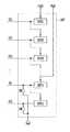
図3を参照すると、本発明の実施例による表示装置は、走査駆動部200、データ駆動部300、発光駆動部400、及びタイミング制御部500を備える。 Referring to FIG. 3, the display device according to the embodiment of the present invention includes a
第1画素PXL1は、走査線S1、S2、第1発光制御線E11、E12、及びデータ線D1〜Dmと接続されるように第1表示領域110に配置される。このような第1画素PXL1は、走査線S1、S2から走査信号が供給されるとき、データ線D1〜Dmからデータ信号の供給を受ける。データ信号の供給を受けた第1画素PXL1は、第1電源ELVDDから有機発光ダイオード(不図示)を経由して第2電源ELVSSに流れる電流量を制御する。このような第1画素PXL1は、第1発光制御線E11、E12から供給される発光制御信号に応じて発光時間が制御される。 The first pixel PXL1 is arranged in the
第1画素PXL1は、IR光源130が駆動される期間中にわたって非発光状態に設定される。このため、発光駆動部400は、IR光源130が駆動される期間中にわたって、第1画素PXL1が非発光状態に設定されるように第1発光制御線E11、E12に供給される発光制御信号を制御する。 The first pixel PXL1 is set to a non-light emitting state during the period in which the IR
例えば、発光駆動部400は、IR光源130の駆動に応じて一フレーム期間のうち第1期間中にわたって第1画素PXL1が非発光状態に設定されるように第1発光制御線E11〜E12に発光制御信号を供給することができる。 For example, the light emitting
また、発光駆動部400は、IR光源130の駆動に応じて一フレーム期間の間第1画素PXL1が発光しないように第1発光制御線E11〜E12に発光制御信号を供給することができる。 Further, the light emitting
一方、図3では、説明の便宜のため、第1画素PXL1が2つの水平ラインに配置されるものが図示されているが、本発明はこれに限定されない。例えば、第1画素PXL1は、少なくとも1つの水平ラインに配置されてもよく、第1画素PXL1の配置に応じて、第1表示領域110に形成される走査線S1、S2及び第1発光制御線E11、E12の数が変更されてもよい。 On the other hand, in FIG. 3, for convenience of explanation, the first pixel PXL1 is arranged on two horizontal lines, but the present invention is not limited to this. For example, the first pixel PXL1 may be arranged in at least one horizontal line, and the scanning lines S1, S2 and the first light emission control line formed in the
第2画素PXL2は、走査線S3〜Sn、第2発光制御線E21〜E2j(jはnより小さい自然数)、及びデータ線D1〜Dmと接続されるように第2表示領域120に配置される。このような第2画素PXL2は、走査線S3〜Snに走査信号が供給されるとき、データ線D1〜Dmからデータ信号の供給を受ける。データ信号の供給を受けた第2画素PXL2は、第1電源ELVDDから有機発光ダイオード(不図示)を経由して第2電源ELVSSに流れる電流量を制御する。このような第2画素PXL2は、第2発光制御線E21〜E2jから供給される発光制御信号に応じて発光時間が制御される。 The second pixel PXL2 is arranged in the
走査駆動部200は、タイミング制御部500からのゲート制御信号GCSに応じて走査線S1〜Snに走査信号を供給する。例えば、走査駆動部200は、走査線S1〜Snに走査信号を順に供給することができる。走査線S1〜Snに走査信号が順に供給されると、水平ライン単位で第1画素PXL1及び第2画素PXL2が順に選択される。このため、走査信号は、画素PXL1、PXL2に含まれたトランジスタがターンオンできるゲートオン電圧に設定される。 The
走査駆動部200は、薄膜工程により周辺領域NAに実装されてもよい。また、走査駆動部200は、画素領域AAと重なるように配置されてもよい。さらに、走査駆動部200は、画素領域AAを挟んで両側に実装されてもよい。 The
発光駆動部400は、タイミング制御部500からのエミッション制御信号ECSに応じて、第1発光制御線E11、E12及び第2発光制御線E21〜E2jに発光制御信号を供給する。例えば、発光駆動部400は、第1発光制御線E11、E12及び第2発光制御線E21〜E2jに発光制御信号を順に供給することができる。発光制御信号は、画素PXL1、PXL2の発光時間を制御するために用いられる。このため、発光制御信号は、画素PXL1、PXL2に含まれたトランジスタがターンオフできるようにゲートオフ電圧に設定されてもよい。 The light
IR光源130が駆動されない期間の間、発光駆動部400は、第2幅の発光制御信号を第1発光制御線E11、E12及び第2発光制御線E21〜E2jに順に供給することができる。ここで、第2幅の発光制御信号は、第1画素PXL1及び第2画素PXL2が、データ信号に応じて所定の映像を表示することができるように設定される。 During the period when the IR
また、発光駆動部400は、IR光源130が駆動される期間の間、第2幅より広い幅の発光制御信号を第1発光制御線E11、E12に供給することができる。例えば、発光駆動部400は、IR光源130が駆動される期間の間、第2幅より広い第1幅の発光制御信号を第1発光制御線E11、E12に供給することができる。ここで、第1幅の発光制御信号は、一フレーム期間に対応して設定されてもよい。したがって、第1幅の発光制御信号が供給されると、第1画素PXL1は一フレーム期間の間非発光状態に設定される。 Further, the light emitting
また、発光駆動部400は、IR光源130の駆動に応じて、第3幅の発光制御信号を第1発光制御線E11、E12に供給することができる。ここで、第3幅は、第2幅より広くて第1幅より狭い第3幅に設定されてもよい。 Further, the light emitting
さらに、第3幅の発光制御信号は、第1表示領域110に位置した第1画素PXL1が一フレームの第1期間の間発光しないように設定される。第3幅の発光制御信号の供給を受けた第1画素PXL1は一フレームの第1期間の間発光せず、第2期間の間データ信号に応じて駆動される。このとき、IR光源130は一フレームの第1期間の間駆動される。 Further, the light emission control signal of the third width is set so that the first pixel PXL1 located in the
発光駆動部400は、薄膜工程により周辺領域NAに実装されてもよい。また、発光駆動部400は、画素領域AAと重なるように配置されてもよい。さらに、発光駆動部400は、画素領域AAを挟んで両側に実装されてもよい。 The light emitting
データ駆動部300は、データ制御信号DCSに応じてデータ線D1〜Dmにデータ信号を供給する。データ線D1〜Dmに供給されたデータ信号は、走査信号によって選択された画素PXL1、PXL2に供給される。ここで、データ駆動部300は、画素領域AAを基準として上側に位置するものが示されているが、本発明はこれに限定されない。例えば、データ駆動部300は、画素領域AAの下側に位置してもよい。 The data drive
タイミング制御部500は、外部から供給されるタイミング信号に基づいてゲート制御信号GCS、エミッション制御信号ECS、及びデータ制御信号DCSを生成する。タイミング制御部500で生成されたゲート制御信号GCSは走査駆動部200に供給され、エミッション制御信号ECSは発光駆動部400に供給される。そして、タイミング制御部500で生成されたデータ制御信号DCSは、データ駆動部300に供給される。 The
図4は、図3に示された第1画素の実施例を示す図である。図4では、説明の便宜のため、第mデータ線Dm及び第1走査線S1に接続された画素を図示する。 FIG. 4 is a diagram showing an embodiment of the first pixel shown in FIG. In FIG. 4, for convenience of explanation, the pixels connected to the mth data line Dm and the first scanning line S1 are illustrated.
図4を参照すると、本発明の実施例による第1画素PXL1は、有機発光ダイオードOLED、駆動トランジスタMD、発光制御トランジスタME、第1トランジスタM1、及びストレージキャパシタCstを備える。 Referring to FIG. 4, the first pixel PXL1 according to the embodiment of the present invention includes an organic light emitting diode OLED, a drive transistor MD, a light emission control transistor ME, a first transistor M1, and a storage capacitor Cst.
有機発光ダイオードOLEDのアノード電極は、駆動トランジスタMDの第2電極に接続され、カソード電極は、第2電源ELVSSに接続される。この有機発光ダイオードOLEDは、駆動トランジスタMDから供給される電流量に応じて所定輝度の光を生成する。このため、第1電源ELVDDは、第2電源ELVSSより高い電圧に設定される。 The anode electrode of the organic light emitting diode OLED is connected to the second electrode of the drive transistor MD, and the cathode electrode is connected to the second power supply ELVSS. The organic light emitting diode OLED generates light having a predetermined brightness according to the amount of current supplied from the drive transistor MD. Therefore, the first power supply EL VDD is set to a voltage higher than that of the second power supply ELVSS.
駆動トランジスタMDの第1電極は、発光制御トランジスタMEを経由して第1電源ELVDDに接続され、第2電極は、有機発光ダイオードOLEDのアノード電極に接続される。また、駆動トランジスタMDのゲート電極は、第1ノードN1に接続される。この駆動トランジスタMDは、第1ノードN1の電圧に応じて、第1電源ELVDDから有機発光ダイオードOLEDを経由して第2電源ELVSSに供給される電流量を制御する。 The first electrode of the drive transistor MD is connected to the first power supply EL VDD via the light emission control transistor ME, and the second electrode is connected to the anode electrode of the organic light emitting diode OLED. Further, the gate electrode of the drive transistor MD is connected to the first node N1. The drive transistor MD controls the amount of current supplied from the first power supply EL VDD to the second power supply ELVSS via the organic light emitting diode OLED according to the voltage of the first node N1.
第1トランジスタM1は、データ線Dmと第1ノードN1との間に接続される。また、第1トランジスタM1のゲート電極は走査線S1に接続される。この第1トランジスタM1は、走査線S1に走査信号が供給されるときターンオンされて、データ線Dmと第1ノードN1を電気的に接続させる。 The first transistor M1 is connected between the data line Dm and the first node N1. Further, the gate electrode of the first transistor M1 is connected to the scanning line S1. The first transistor M1 is turned on when a scanning signal is supplied to the scanning line S1 to electrically connect the data line Dm and the first node N1.
発光制御トランジスタMEは、第1電源ELVDDと駆動トランジスタMDの第1電極との間に接続される。また、発光制御トランジスタMEのゲート電極は、最初の第1発光制御線E11に接続される。この発光制御トランジスタMEは、最初の第1発光制御線E11に発光制御信号が供給されるときターンオフされ、発光制御信号が供給されないときターンオンされる。 The light emission control transistor ME is connected between the first power supply EL VDD and the first electrode of the drive transistor MD. Further, the gate electrode of the light emission control transistor ME is connected to the first light emission control line E11. The light emission control transistor ME is turned off when a light emission control signal is supplied to the first first light emission control line E11, and is turned on when a light emission control signal is not supplied.
ストレージキャパシタCstは、第1電源ELVDDと第1ノードN1との間に接続される。このストレージキャパシタCstは、データ信号に対応する電圧を保存する。 The storage capacitor Cst is connected between the first power supply EL VDD and the first node N1. This storage capacitor Cst stores the voltage corresponding to the data signal.
一方、第2画素PXL2は、第1画素PXL1と同じ回路で実現されてもよい。したがって、第2画素PXL2に対する詳細な説明は省略する。 On the other hand, the second pixel PXL2 may be realized by the same circuit as the first pixel PXL1. Therefore, a detailed description of the second pixel PXL2 will be omitted.
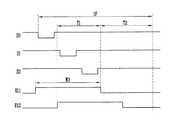
図5aは、図4に示された第1画素の駆動方法の実施例を示す図である。図5aには、最初の第1発光制御線E11に第2幅の発光制御信号が供給される場合が図示されている。 FIG. 5a is a diagram showing an embodiment of the driving method of the first pixel shown in FIG. FIG. 5a illustrates a case where a light emission control signal having a second width is supplied to the first light emission control line E11.
図5aを参照すると、まず、最初の第1発光制御線E11に第2幅W2を有する発光制御信号が供給される。最初の第1発光制御線E11に発光制御信号が供給されると、発光制御トランジスタMEがターンオフされる。 Referring to FIG. 5a, first, a light emission control signal having a second width W2 is supplied to the first first light emission control line E11. When a light emission control signal is supplied to the first first light emission control line E11, the light emission control transistor ME is turned off.
その後、走査線S1に走査信号が供給される。走査線S1に走査信号が供給されると、第1トランジスタM1がターンオンされる。第1トランジスタM1がターンオンされると、データ線Dmからのデータ信号DSが第1ノードN1に供給される。このとき、ストレージキャパシタCstは、第1ノードN1に供給されたデータ信号DSの電圧を保存する。 After that, a scanning signal is supplied to the scanning line S1. When a scanning signal is supplied to the scanning line S1, the first transistor M1 is turned on. When the first transistor M1 is turned on, the data signal DS from the data line Dm is supplied to the first node N1. At this time, the storage capacitor Cst stores the voltage of the data signal DS supplied to the first node N1.
ストレージキャパシタCstにデータ信号DSの電圧が保存された後、最初の第1発光制御線E11への発光制御信号の供給が中断される。最初の第1発光制御線E11への発光制御信号の供給が中断されると、発光制御トランジスタMEがターンオンされる。発光制御トランジスタMEがターンオンされると、第1電源ELVDDと駆動トランジスタMDが電気的に接続される。このとき、駆動トランジスタMDは、第1ノードN1の電圧に応じて有機発光ダイオードOLEDに供給される電流量を制御する。そうすると、有機発光ダイオードOLEDは、駆動トランジスタMDに供給される電流量に応じて発光する。IR光源130が駆動されない期間の間、第1画素PXL1及び第2画素PXL2は上述した方法で駆動されうる。 After the voltage of the data signal DS is stored in the storage capacitor Cst, the supply of the light emission control signal to the first light emission control line E11 is interrupted. When the supply of the light emission control signal to the first light emission control line E11 is interrupted, the light emission control transistor ME is turned on. When the light emission control transistor ME is turned on, the first power supply EL VDD and the drive transistor MD are electrically connected. At this time, the drive transistor MD controls the amount of current supplied to the organic light emitting diode OLED according to the voltage of the first node N1. Then, the organic light emitting diode OLED emits light according to the amount of current supplied to the drive transistor MD. During the period when the IR
一方、IR光源130が駆動される期間には、IRが第1画素PXL1の第1トランジスタM1に照射される。IRが第1トランジスタM1に照射されると、第1トランジスタM1でリーク電流が発生し、これにより、第1ノードN1の電圧が変化する。即ち、IR光源130が駆動される期間の間、第1画素PXL1は所望する輝度で発光されないため、画質が低下する恐れがある。 On the other hand, during the period when the IR
図5bは、図4に示した第1画素の駆動方法の他の実施例を示す図である。図5bには、IR光源130の駆動に応じて、最初の第1発光制御線E11に、第1幅W1の発光制御信号が供給される場合が図示されている。 FIG. 5b is a diagram showing another embodiment of the driving method of the first pixel shown in FIG. FIG. 5b illustrates a case where a light emission control signal having a first width W1 is supplied to the first first light emission control line E11 in response to driving of the IR
図5bを参照すると、まず、最初の第1発光制御線E11に第1幅W1を有する発光制御信号が供給される。最初の第1発光制御線E11に、第1幅W1を有する発光制御信号が供給されると、発光制御トランジスタMEがターンオフされる。 Referring to FIG. 5b, first, a light emission control signal having a first width W1 is supplied to the first first light emission control line E11. When a light emission control signal having a first width W1 is supplied to the first light emission control line E11, the light emission control transistor ME is turned off.
ここで、第1幅W1は、一フレーム1F期間中にわたって第1画素PXL1がターンオフされるように設定される。即ち、第1幅W1の発光制御信号の供給を受けた発光制御トランジスタMEは、一フレーム1F期間中にわたってターンオフ状態を保持する。そうすると、第1画素PXL1は、データ線Dmに供給されるデータ信号DSに関わらず、一フレーム1F期間中にわたって非発光状態を保持する。 Here, the first width W1 is set so that the first pixel PXL1 is turned off during the period of one
即ち、IR光源130が駆動される期間の間、第1画素PXL1は非発光状態に設定されるため、第1画素PXL1が所望しない輝度で発光することを防ぐことができる。 That is, since the first pixel PXL1 is set to the non-light emitting state during the period in which the IR
図5cは、図4に示した第1画素の駆動方法のさらに他の実施例を示す図である。図5cには、IR光源130の駆動に応じて第3幅W3の発光制御信号が供給される場合が図示されている。 FIG. 5c is a diagram showing still another embodiment of the method of driving the first pixel shown in FIG. FIG. 5c shows a case where a light emission control signal having a third width W3 is supplied according to the drive of the IR
図5cを参照すると、第1発光制御線E11、E12には第3幅W3の発光制御信号が順に供給される。このとき、第1発光制御線E11、E12に供給される発光制御信号は、一フレーム1F期間のうち第1期間T1と重なる。従って、一フレーム1F期間のうち第1期間T1の間、第1画素PXL1は非発光状態に設定される。IR光源130は、一フレーム期間のうち第1期間T1の間駆動される。 Referring to FIG. 5c, light emission control signals having a third width W3 are sequentially supplied to the first light emission control lines E11 and E12. At this time, the light emission control signal supplied to the first light emission control lines E11 and E12 overlaps with the first period T1 in one
また、一フレーム1F期間のうち第2期間T2の間、第1画素PXL1はデータ信号に応じて順に駆動される。 Further, during the second period T2 of the one
即ち、本発明のさらに他の実施例では、一フレーム1F期間のうち第1期間T1の間、第1画素PXL1が非発光状態に設定され、これに応じてIR光源130が駆動される。そして、一フレーム1F期間のうち第2期間T2の間、第1画素PXL1はデータ信号に応じて駆動される。 That is, in still another embodiment of the present invention, the first pixel PXL1 is set to the non-emission state during the first period T1 of the one
さらに、発光制御信号の第3幅W3は、第1画素PXL1が同時に非発光状態に設定できるように実験的に決まる。例えば、第3幅W3は、第1発光制御線E11、E12の数に応じて多様に設定されてもよい。 Further, the third width W3 of the light emission control signal is experimentally determined so that the first pixel PXL1 can be set to the non-light emission state at the same time. For example, the third width W3 may be variously set according to the number of the first light emission control lines E11 and E12.
図6aは、図3に示された第1画素の他の実施例を示す図である。図6aでは、図4と同様の構成に対して同じ符号を付し、詳細な説明は省略する。 FIG. 6a is a diagram showing another embodiment of the first pixel shown in FIG. In FIG. 6a, the same reference numerals are given to the same configurations as in FIG. 4, and detailed description thereof will be omitted.
図6aを参照すると、本発明の実施例による第1画素PXL1は、有機発光ダイオードOLED、駆動トランジスタMD、発光制御トランジスタME’、及び第1トランジスタM1を備える。 Referring to FIG. 6a, the first pixel PXL1 according to the embodiment of the present invention includes an organic light emitting diode OLED, a drive transistor MD, a light emission control transistor ME', and a first transistor M1.
発光制御トランジスタME’は、駆動トランジスタMDの第2電極と有機発光ダイオードOLEDのアノード電極との間に接続される。また、発光制御トランジスタME’のゲート電極は、最初の発光制御線E11に接続される。この発光制御トランジスタME’は、最初の第1発光制御線E11に発光制御信号が供給されるときターンオフされ、発光制御信号が供給されないときターンオンされる。 The light emission control transistor ME'is connected between the second electrode of the drive transistor MD and the anode electrode of the organic light emitting diode OLED. Further, the gate electrode of the light emission control transistor ME'is connected to the first light emission control line E11. The light emission control transistor ME'is turned off when a light emission control signal is supplied to the first first light emission control line E11, and is turned on when a light emission control signal is not supplied.
一方、本発明の実施例において、発光制御トランジスタは、第1電源ELVDDから有機発光ダイオードOLEDを経由して第2電源ELVSSに繋がる電流経路に多様に配置されてもよい。 On the other hand, in the embodiment of the present invention, the light emission control transistor may be variously arranged in the current path from the first power supply EL VDD to the second power supply ELVSS via the organic light emitting diode OLED.
例えば、図6bに示すように、第1電源ELVDDと駆動トランジスタMDの第1電極との間に第1発光制御トランジスタME1が形成され、駆動トランジスタMDの第2電極と有機発光ダイオードOLEDのアノード電極との間に第2発光制御トランジスタME2が形成されてもよい。第1発光制御トランジスタME1及び第2発光制御トランジスタME2のゲート電極は、最初の第1発光制御線E11に接続される。従って、第1発光制御トランジスタME1及び第2発光制御トランジスタME2は、最初の第1発光制御線E11に供給される発光制御信号に応じてターンオン及びターンオフされる。 For example, as shown in FIG. 6b, the first light emission control transistor ME1 is formed between the first power supply EL VDD and the first electrode of the drive transistor MD, and the second electrode of the drive transistor MD and the anode electrode of the organic light emitting diode OLED are formed. The second light emission control transistor ME2 may be formed between the two. The gate electrodes of the first light emission control transistor ME1 and the second light emission control transistor ME2 are connected to the first light emission control line E11. Therefore, the first light emission control transistor ME1 and the second light emission control transistor ME2 are turned on and off according to the light emission control signal supplied to the first light emission control line E11.
実際に、図6a及び図6bに示された第1画素PXL1の動作過程は、図5a〜図5cとともに説明した図4の画素と同一であるため、詳細な説明は省略する。 Actually, the operation process of the first pixel PXL1 shown in FIGS. 6a and 6b is the same as that of the pixel of FIG. 4 described with FIGS. 5a to 5c, and therefore detailed description thereof will be omitted.
図7は、図3に示された第1画素のさらに他の実施例を示す図である。図7では、説明の便宜のため、第mデータ線及び第1走査線S1に接続された画素を図示する。また、図6bと同じ機能をするトランジスタには同じ符号を付する。さらに、図7に示された第0走査線S0は、第1画素PXL1の回路構造に応じて画素領域AAにさらに形成された走査線を意味する。 FIG. 7 is a diagram showing still another embodiment of the first pixel shown in FIG. In FIG. 7, for convenience of explanation, the pixels connected to the m-th data line and the first scanning line S1 are shown. Further, the transistors having the same functions as those in FIG. 6b are designated by the same reference numerals. Further, the 0th scanning line S0 shown in FIG. 7 means a scanning line further formed in the pixel region AA according to the circuit structure of the first pixel PXL1.
図7を参照すると、本発明のさらに他の実施例による第1画素PXL1は、有機発光ダイオードOLED、駆動トランジスタMD、発光制御トランジスタME1、ME2、第1トランジスタM1乃至第4トランジスタM4、ストレージキャパシタCstを備える。 Referring to FIG. 7, the first pixel PXL1 according to still another embodiment of the present invention includes an organic light emitting diode OLED, a drive transistor MD, a light emitting control transistor ME1 and ME2, a first transistor M1 to a fourth transistor M4, and a storage capacitor Cst. To be equipped with.
有機発光ダイオードOLEDのアノード電極は、第2発光制御トランジスタME2を経由して駆動トランジスタMDの第2電極に接続され、カソード電極は、第2電源ELVSSに接続される。この有機発光ダイオードOLEDは、駆動トランジスタMDから供給される電流量に応じて所定輝度の光を生成する。 The anode electrode of the organic light emitting diode OLED is connected to the second electrode of the drive transistor MD via the second light emitting control transistor ME2, and the cathode electrode is connected to the second power supply ELVSS. The organic light emitting diode OLED generates light having a predetermined brightness according to the amount of current supplied from the drive transistor MD.
駆動トランジスタMDの第1電極は、第1発光制御トランジスタME1を経由して第1電源ELVDDに接続され、第2電極は、第2発光制御トランジスタME2を経由して有機発光ダイオードOLEDのアノード電極に接続される。また、駆動トランジスタMDのゲート電極は、第1ノードN1に接続される。この駆動トランジスタMDは、第1ノードN1の電圧に応じて、第1電源ELVDDから有機発光ダイオードOLEDを経由して第2電源ELVSSに供給される電流量を制御する。 The first electrode of the drive transistor MD is connected to the first power supply EL VDD via the first light emission control transistor ME1, and the second electrode is connected to the anode electrode of the organic light emitting diode OLED via the second light emission control transistor ME2. Be connected. Further, the gate electrode of the drive transistor MD is connected to the first node N1. The drive transistor MD controls the amount of current supplied from the first power supply EL VDD to the second power supply ELVSS via the organic light emitting diode OLED according to the voltage of the first node N1.
第1発光制御トランジスタME1は、第1電源ELVDDと第2ノードN2との間に接続される。また、第1発光制御トランジスタME1のゲート電極は、最初の第1発光制御線E11に接続される。この第1発光制御トランジスタME1は、最初の第1発光制御線E11に発光制御信号が供給されるときターンオフされ、それ以外の場合はターンオンされる。 The first light emission control transistor ME1 is connected between the first power supply EL VDD and the second node N2. Further, the gate electrode of the first light emission control transistor ME1 is connected to the first light emission control line E11. The first light emission control transistor ME1 is turned off when a light emission control signal is supplied to the first first light emission control line E11, and is turned on in other cases.
第2発光制御トランジスタME2は、駆動トランジスタMDの第2電極と、有機発光ダイオードOLEDのアノード電極との間に接続される。また、第2発光制御トランジスタME2のゲート電極は、最初の第1発光制御線E11に接続される。この第2発光制御トランジスタME2は、最初の第1発光制御線E11に発光制御信号が供給されるときターンオフされ、それ以外の場合はターンオンされる。 The second light emission control transistor ME2 is connected between the second electrode of the drive transistor MD and the anode electrode of the organic light emitting diode OLED. Further, the gate electrode of the second light emission control transistor ME2 is connected to the first light emission control line E11. The second light emission control transistor ME2 is turned off when a light emission control signal is supplied to the first first light emission control line E11, and is turned on in other cases.
第1トランジスタM1は、データ線Dmと第2ノードN2との間に接続される。また、第1トランジスタM1のゲート電極は走査線S1に接続される。この第1トランジスタM1は、走査線S1に走査信号が供給されるときにターンオンされて、データ線Dmと第2ノードN2を電気的に接続させる。 The first transistor M1 is connected between the data line Dm and the second node N2. Further, the gate electrode of the first transistor M1 is connected to the scanning line S1. The first transistor M1 is turned on when a scanning signal is supplied to the scanning line S1 to electrically connect the data line Dm and the second node N2.
第2トランジスタM2は、駆動トランジスタMDの第2電極と第1ノードN1との間に接続される。また、第2トランジスタM2のゲート電極は走査線S1に接続される。この第2トランジスタM2は、走査線S1に走査信号が供給されるときにターンオンされて、駆動トランジスタMDをダイオード接続させる。 The second transistor M2 is connected between the second electrode of the drive transistor MD and the first node N1. Further, the gate electrode of the second transistor M2 is connected to the scanning line S1. The second transistor M2 is turned on when a scanning signal is supplied to the scanning line S1 to connect the drive transistor MD to a diode.
第3トランジスタM3の第1電極は第1ノードN1に接続され、第2電極は初期化電源Vintに接続される。また、第3トランジスタM3のゲート電極は走査線S0に接続される。この第3トランジスタM3は、走査線S0に走査信号が供給されるときターンオンされて、初期化電源Vintの電圧を第1ノードN1に供給する。ここで、初期化電源Vintの電圧は、データ信号より低い電圧に設定される。 The first electrode of the third transistor M3 is connected to the first node N1, and the second electrode is connected to the initialization power supply Vint. Further, the gate electrode of the third transistor M3 is connected to the scanning line S0. The third transistor M3 is turned on when a scanning signal is supplied to the scanning line S0, and supplies the voltage of the initialization power supply Vint to the first node N1. Here, the voltage of the initialization power supply Vint is set to a voltage lower than the data signal.
第4トランジスタM4は、有機発光ダイオードOLEDのアノード電極と初期化電源Vintとの間に接続される。また、第4トランジスタM4のゲート電極は走査線S1に接続される。この第4トランジスタM4は、走査線S1に走査信号が供給されるときにターンオンされて、初期化電源Vintの電圧を有機発光ダイオードOLEDのアノード電極に供給する。 The fourth transistor M4 is connected between the anode electrode of the organic light emitting diode OLED and the initialization power supply Vint. Further, the gate electrode of the fourth transistor M4 is connected to the scanning line S1. The fourth transistor M4 is turned on when a scanning signal is supplied to the scanning line S1 to supply the voltage of the initialization power supply Vint to the anode electrode of the organic light emitting diode OLED.
初期化電源Vintの電圧が有機発光ダイオードOLEDのアノード電極に供給されると、有機発光ダイオードOLEDの寄生キャパシタColedが放電されるため、ブラック表現能力を向上させることができる。 When the voltage of the initialization power supply Vint is supplied to the anode electrode of the organic light emitting diode OLED, the parasitic capacitor Cold of the organic light emitting diode OLED is discharged, so that the black expression ability can be improved.
さらに、第4トランジスタM4のゲート電極は、様々な走査線と接続されてもよい。例えば、第4トランジスタM4は、最初の第1発光制御線E11に供給される発光制御信号と重なる走査信号のいずれか1つによってターンオンされうる。 Further, the gate electrode of the fourth transistor M4 may be connected to various scanning lines. For example, the fourth transistor M4 can be turned on by any one of the scanning signals that overlaps the light emission control signal supplied to the first light emission control line E11.
ストレージキャパシタCstは、第1電源ELVDDと第1ノードN1との間に接続される。このストレージキャパシタCstは、第1ノードN1に印加される電圧を保存する。 The storage capacitor Cst is connected between the first power supply EL VDD and the first node N1. This storage capacitor Cst stores the voltage applied to the first node N1.
一方、第2画素PXL2は、第1画素PXL1と同じ回路で実現されてもよい。従って、第2画素PXL2に対する詳細な説明は省略する。 On the other hand, the second pixel PXL2 may be realized by the same circuit as the first pixel PXL1. Therefore, a detailed description of the second pixel PXL2 will be omitted.
図8aは、図7に示された第1画素の駆動方法の実施例を示す図である。図8aには、最初の第1発光制御線E11に第2幅W2の発光制御信号が供給される場合が図示されている。 FIG. 8a is a diagram showing an embodiment of the driving method of the first pixel shown in FIG. 7. FIG. 8a illustrates a case where a light emission control signal having a second width W2 is supplied to the first light emission control line E11.
図8aを参照すると、まず、最初の第1発光制御線E11に発光制御信号が供給され、第1発光制御トランジスタME1及び第2発光制御トランジスタME2がターンオフされる。第1発光制御トランジスタME1がターンオフされると、第1電源ELVDDと第2ノードN2が電気的に遮断される。第2発光制御トランジスタME2がターンオフされると、駆動トランジスタMDと有機発光ダイオードOLEDが電気的に遮断される。従って、最初の第1発光制御線E11に発光制御信号が供給される期間の間、第1画素PXL1は非発光状態に設定される。 Referring to FIG. 8a, first, a light emission control signal is supplied to the first first light emission control line E11, and the first light emission control transistor ME1 and the second light emission control transistor ME2 are turned off. When the first light emission control transistor ME1 is turned off, the first power supply EL VDD and the second node N2 are electrically cut off. When the second light emission control transistor ME2 is turned off, the drive transistor MD and the organic light emitting diode OLED are electrically cut off. Therefore, during the period in which the light emission control signal is supplied to the first light emission control line E11, the first pixel PXL1 is set to the non-light emission state.
その後、第0走査線S0に走査信号が供給される。第0走査線S0に走査信号が供給されると、第3トランジスタM3がターンオンされる。第3トランジスタM3がターンオンされると、初期化電源Vintの電圧が第1ノードN1に供給される。 After that, a scanning signal is supplied to the 0th scanning line S0. When a scanning signal is supplied to the 0th scanning line S0, the third transistor M3 is turned on. When the third transistor M3 is turned on, the voltage of the initialization power supply Vint is supplied to the first node N1.
第1ノードN1に初期化電源Vintの電圧が供給された後、第1走査線S1に走査信号が供給される。第1走査線S1に走査信号が供給されると、第1トランジスタM1、第2トランジスタM2、及び第4トランジスタM4がターンオンされる。 After the voltage of the initialization power supply Vint is supplied to the first node N1, the scanning signal is supplied to the first scanning line S1. When a scanning signal is supplied to the first scanning line S1, the first transistor M1, the second transistor M2, and the fourth transistor M4 are turned on.
第4トランジスタM4がターンオンされると、有機発光ダイオードOLEDのアノード電極に初期化電源Vintの電圧が供給され、これにより、寄生キャパシタColedが放電される。 When the fourth transistor M4 is turned on, the voltage of the initialization power supply Vint is supplied to the anode electrode of the organic light emitting diode OLED, whereby the parasitic capacitor Cold is discharged.
第2トランジスタM2がターンオンされると、駆動トランジスタMDがダイオード接続される。第1トランジスタM1がターンオンされると、データ線Dmからのデータ信号DSが第2ノードN2に供給される。このとき、第1ノードN1がデータ信号より低い初期化電源Vintの電圧に初期化されているため、駆動トランジスタMDがターンオンされる。 When the second transistor M2 is turned on, the drive transistor MD is connected to the diode. When the first transistor M1 is turned on, the data signal DS from the data line Dm is supplied to the second node N2. At this time, since the first node N1 is initialized to the voltage of the initialization power supply Vint lower than the data signal, the drive transistor MD is turned on.
駆動トランジスタMDがターンオンされると、第2ノードN2に供給されたデータ信号が、ダイオード接続された駆動トランジスタMDを経由して、第1ノードN1に供給される。このとき、第1ノードN1には、データ信号及び駆動トランジスタMDのしきい値電圧に対応する電圧が印加される。ストレージキャパシタCstは、第1ノードN1に印加された電圧を保存する。 When the drive transistor MD is turned on, the data signal supplied to the second node N2 is supplied to the first node N1 via the diode-connected drive transistor MD. At this time, a voltage corresponding to the data signal and the threshold voltage of the drive transistor MD is applied to the first node N1. The storage capacitor Cst stores the voltage applied to the first node N1.
ストレージキャパシタCstにデータ信号及び駆動トランジスタMDのしきい値電圧に対応する電圧が保存された後、最初の第1発光制御線E11への発光制御信号の供給が中断される。最初の第1発光制御線E11への発光制御信号の供給が中断されると、第1発光制御トランジスタME1及び第2発光制御トランジスタME2がターンオンされる。 After the data signal and the voltage corresponding to the threshold voltage of the drive transistor MD are stored in the storage capacitor Cst, the supply of the light emission control signal to the first light emission control line E11 is interrupted. When the supply of the light emission control signal to the first light emission control line E11 is interrupted, the first light emission control transistor ME1 and the second light emission control transistor ME2 are turned on.
第1発光制御トランジスタME1がターンオンされると、第1電源ELVDDと駆動トランジスタMDの第1電極が電気的に接続される。第2発光制御トランジスタME2がターンオンされると、駆動トランジスタMDの第2電極と有機発光ダイオードOLEDのアノード電極が電気的に接続される。このとき、駆動トランジスタMDは、第1ノードN1に印加された電圧に応じて、第1電源ELVDDから有機発光ダイオードOLEDを経由して第2電源ELVSSに流れる電流量を制御する。 When the first light emission control transistor ME1 is turned on, the first power supply EL VDD and the first electrode of the drive transistor MD are electrically connected. When the second light emission control transistor ME2 is turned on, the second electrode of the drive transistor MD and the anode electrode of the organic light emitting diode OLED are electrically connected. At this time, the drive transistor MD controls the amount of current flowing from the first power supply EL VDD to the second power supply ELVSS via the organic light emitting diode OLED according to the voltage applied to the first node N1.
IR光源130が駆動されない期間の間、第1画素PXL1及び第2画素PXL2は上述した方法で駆動されうる。 During the period when the IR
一方、IR光源130が駆動される期間には、IRが第1画素PXL1に照射されるため、第1トランジスタM1、第2トランジスタM2、第3トランジスタM3でリーク電流が発生する。 On the other hand, during the period when the IR
特に、第2トランジスタM2及び第3トランジスタM3によるリーク電流によって、第1ノードN1の電圧は一フレーム1F期間の間低くなり続ける。駆動トランジスタMDから有機発光ダイオードOLEDに流れる電流は、駆動トランジスタMDのVgs電圧から駆動トランジスタMDのしきい値電圧を引いた電圧の二乗に比例する。従って、第1ノードN1の電圧が低くなると、駆動トランジスタMDから流れる電流は二乗に比例して増加し、これにより、第1画素PXL1が明点としてユーザに認知されうる。 In particular, due to the leakage current due to the second transistor M2 and the third transistor M3, the voltage of the first node N1 continues to decrease during one
図8bは、図7に示された第1画素の駆動方法の他の実施例を示す図である。図8bには、IR光源130の駆動に応じて、最初の第1発光制御線E11に第1幅W1の発光制御信号が供給される場合が図示されている。 FIG. 8b is a diagram showing another embodiment of the driving method of the first pixel shown in FIG. 7. FIG. 8b shows a case where a light emission control signal having a first width W1 is supplied to the first first light emission control line E11 in response to driving of the IR
図8bを参照すると、まず、最初の第1発光制御線E11に第1幅W1を有する発光制御信号が供給される。最初の第1発光制御線E11に第1幅W1を有する発光制御信号が供給されると、第1発光制御トランジスタME1及び第2発光制御トランジスタME2がターンオフされる。 Referring to FIG. 8b, first, a light emission control signal having a first width W1 is supplied to the first first light emission control line E11. When a light emission control signal having a first width W1 is supplied to the first light emission control line E11, the first light emission control transistor ME1 and the second light emission control transistor ME2 are turned off.
第1発光制御トランジスタME1及び第2発光制御トランジスタME2がターンオフされると、第1画素PXL1が非発光状態に設定される。ここで、第1幅W1は、一フレーム1F期間の間、第1画素PXL1がターンオフできるように設定される。即ち、第1幅W1の発光制御信号の供給を受けた第1及び第2発光制御トランジスタME1、ME2は、一フレーム1F期間の間ターンオフ状態を保持する。そうすると、第1画素PXL1は、データ線Dmに供給されるデータ信号DSに関わらず、一フレーム1F期間中にわたって非発光状態を保持する。 When the first light emission control transistor ME1 and the second light emission control transistor ME2 are turned off, the first pixel PXL1 is set to the non-light emission state. Here, the first width W1 is set so that the first pixel PXL1 can be turned off during the period of one
即ち、IR光源130が駆動される期間中にわたって、第1画素PXL1は非発光状態に設定されるため、第1画素PXL1が所望しない輝度で発光することを防ぐことができる。 That is, since the first pixel PXL1 is set to the non-light emitting state during the period in which the IR
図8cは、図7に示された第1画素の駆動方法のさらに他の実施例を示す図である。図8cには、IR光源130の駆動に応じて、第3幅W3の発光制御信号が供給される場合が図示されている。 FIG. 8c is a diagram showing still another embodiment of the method of driving the first pixel shown in FIG. 7. FIG. 8c shows a case where a light emission control signal having a third width W3 is supplied according to the driving of the IR
図8cを参照すると、第1発光制御線E11、E12には第3幅W3の発光制御信号が順に供給される。このとき、第1発光制御線E11、E12に供給される発光制御信号は、一フレーム1F期間のうち第1期間T1と重なる。したがって、一フレーム1F期間のうち第1期間T1中にわたって、第1画素PXL1は非発光状態に設定される。IR光源130は一フレーム期間のうち第1期間T1の間駆動される。 Referring to FIG. 8c, light emission control signals having a third width W3 are sequentially supplied to the first light emission control lines E11 and E12. At this time, the light emission control signal supplied to the first light emission control lines E11 and E12 overlaps with the first period T1 in one
また、一フレーム1F期間のうち第2期間T2の間、第1画素PXL1はデータ信号に応じて順に駆動される。即ち、本発明のさらに他の実施例では、一フレーム1F期間のうち第1期間T1中にわたって、第1画素PXL1が非発光状態に設定され、これに応じてIR光源130が駆動される。そして、一フレーム1F期間のうち第2期間T2の間、第1画素PXL1はデータ信号に応じて駆動される。 Further, during the second period T2 of the one
図9は、図3に示された発光駆動部の実施例を示す図である。図9に示されたステージEST11、EST12、EST21〜EST2jは、開始信号FLM1、FLM2に応じて発光制御信号の幅を制御する回路構造を有する。このようなステージEST11、EST12、EST21〜EST2jは、開始信号FLM1、FLM2に応じて発光制御信号の幅を制御する、現在公知の多様な回路で構成されてもよい。 FIG. 9 is a diagram showing an embodiment of the light emitting drive unit shown in FIG. The stages EST11, EST12, EST21 to EST2j shown in FIG. 9 have a circuit structure for controlling the width of the light emission control signal according to the start signals FLM1 and FLM2. Such stages EST11, EST12, EST21 to EST2j may be composed of various currently known circuits that control the width of the light emission control signal according to the start signals FLM1 and FLM2.
また、ステージEST11、EST12、EST21〜EST2jは、開始信号FLM1、FLM2に応じて同一または類似する幅を有する発光制御信号を生成する。以下では、説明の便宜のため、ステージEST11、EST12、EST21〜EST2jは、開始信号FLM1、FLM2と同じ幅を有する発光制御信号を生成すると仮定する。 Further, the stages EST11, EST12, EST21 to EST2j generate a light emission control signal having the same or similar width depending on the start signals FLM1 and FLM2. In the following, for convenience of explanation, it is assumed that the stages EST11, EST12, EST21 to EST2j generate a light emission control signal having the same width as the start signals FLM1 and FLM2.
図9を参照すると、本発明の実施例による発光駆動部400は、第1発光ステージEST11、EST12及び第2発光ステージEST21〜EST2jを備える。 Referring to FIG. 9, the light emitting
第1発光ステージEST11、EST12は、第1発光制御線E11、E12のそれぞれと接続される。この第1発光ステージEST11、EST12は、第1開始信号FLM1によって駆動される。即ち、最初の第1発光ステージEST11は、第1開始信号FLM1に応じて発光制御信号を出力する。そして、二番目の第1発光ステージEST12は、最初の第1発光ステージEST11の出力信号(即ち、発光制御信号)の供給を受け、供給された出力信号に応じて発光制御信号を出力する。 The first light emitting stages EST11 and EST12 are connected to the first light emitting control lines E11 and E12, respectively. The first light emitting stages EST11 and EST12 are driven by the first start signal FLM1. That is, the first first light emitting stage EST11 outputs a light emitting control signal in response to the first start signal FLM1. Then, the second first light emitting stage EST12 receives the supply of the output signal (that is, the light emitting control signal) of the first first light emitting stage EST11, and outputs the light emitting control signal according to the supplied output signal.
さらに、第1発光ステージEST11、EST12から供給される発光制御信号の幅は、第1開始信号FLM1に応じて決まる。即ち、第1幅W1の第1開始信号FLM1が供給される場合、第1発光制御線E11、E12には第1幅W1の発光制御信号が供給される。そして、第2幅W2の第1開始信号FLM1が供給される場合、第1発光制御線E11、E12には第2幅W2の発光制御信号が供給される。同様に、第3幅W3の第1開始信号FLM1が供給される場合、第1発光制御線E11、E12には第3幅W3の発光制御信号が供給される。 Further, the width of the light emission control signal supplied from the first light emission stages EST11 and EST12 is determined according to the first start signal FLM1. That is, when the first start signal FLM1 of the first width W1 is supplied, the light emission control signal of the first width W1 is supplied to the first light emission control lines E11 and E12. Then, when the first start signal FLM1 of the second width W2 is supplied, the light emission control signal of the second width W2 is supplied to the first light emission control lines E11 and E12. Similarly, when the first start signal FLM1 of the third width W3 is supplied, the light emission control signal of the third width W3 is supplied to the first light emission control lines E11 and E12.
第1開始信号FLM1は、タイミング制御部500から供給されてもよい。タイミング制御部500は、IR光源130が駆動されない期間の間、第2幅W2に対応する第1開始信号FLM1を供給する。また、タイミング制御部500は、IR光源130の駆動に応じて第1幅W1または第3幅W3の第1開始信号FLM1を供給することができる。 The first start signal FLM1 may be supplied from the
第2発光ステージEST21〜EST2jは、第2発光制御線E21〜E2jのそれぞれと接続される。この第2発光ステージEST21〜EST2jは、第2開始信号FLM2に応じて駆動される。即ち、最初の第2発光ステージEST21は、第2開始信号FLM2に応じて発光制御信号を出力し、残りの第2発光ステージEST22〜EST2jは、前段の第2発光ステージEST2の出力信号の供給を受けて発光制御信号を出力する。 The second light emitting stages EST21 to EST2j are connected to each of the second light emitting control lines E21 to E2j. The second light emitting stages EST21 to EST2j are driven in response to the second start signal FLM2. That is, the first second light emitting stage EST21 outputs a light emitting control signal in response to the second start signal FLM2, and the remaining second light emitting stages EST22 to EST2j supply the output signal of the second light emitting stage EST2 in the previous stage. Receives and outputs a light emission control signal.
タイミング制御部500は、IR光源130の駆動有無に関わらず、第2幅W2の第2開始信号FLM2を供給する。そうすると、第2発光ステージEST21〜EST2jは、第2幅W2の発光制御信号を、第2発光制御線E21〜E2jに順に供給する。 The
一方、図9では、2つの表示領域110、120に対応して2つの開始信号FLM1、FLM2が発光駆動部400に供給されると説明したが、本願発明はこれに限定されない。例えば、表示パネル100がk(kは2以上の自然数)個の表示領域に分割される場合、発光駆動部400はk個の開始信号FLM1、・・・FLMkによって駆動されてもよい。 On the other hand, in FIG. 9, it has been described that the two start signals FLM1 and FLM2 are supplied to the light emitting
図10aは、図9に示された発光駆動部の駆動方法の実施例を示す図である。図10aには、IR光源130が駆動されず、第1発光制御線E11、E12に第2幅W2の発光制御信号が供給される場合が図示されている。 FIG. 10a is a diagram showing an embodiment of a method of driving the light emitting driving unit shown in FIG. FIG. 10a shows a case where the IR
図10aを参照すると、タイミング制御部500は、第2幅W2の第1開始信号FLM1及び第2開始信号FLM2を発光駆動部400に供給する。ここで、第1開始信号FLM1及び第2開始信号FLM2の供給タイミングは、第1発光制御線E11、E12及び第2発光制御線E21〜E2jに発光制御信号が順に供給されるように制御されてもよい。 Referring to FIG. 10a, the
第2幅W2の第1開始信号FLM1が供給されると、第1発光ステージEST11、EST12は第1発光制御線E11、E12に第2幅W2の発光制御信号を順に供給する。 When the first start signal FLM1 of the second width W2 is supplied, the first light emitting stages EST11 and EST12 sequentially supply the light emission control signals of the second width W2 to the first light emitting control lines E11 and E12.
第2幅W2に対応する第2開始信号FLM2が供給されると、第2発光ステージEST21〜EST2jは第2発光制御線E21〜E2jに第2幅W2の発光制御信号を順に供給する。そうすると、第1表示領域110及び第2表示領域120に所定輝度の映像が表示される。 When the second start signal FLM2 corresponding to the second width W2 is supplied, the second light emitting stages EST21 to EST2j sequentially supply the light emission control signals of the second width W2 to the second light emitting control lines E21 to E2j. Then, an image having a predetermined brightness is displayed in the
図10bは、図9に示された発光駆動部の駆動方法の他の実施例を示す図である。図10bには、第1発光制御線E11、E12に第1幅W1の発光制御信号が供給される場合が図示されている。 FIG. 10b is a diagram showing another embodiment of the driving method of the light emitting driving unit shown in FIG. FIG. 10b illustrates a case where a light emission control signal having a first width W1 is supplied to the first light emission control lines E11 and E12.
図10bを参照すると、タイミング制御部500は、第1幅W1に対応する第1開始信号FLM1及び第2幅W2に対応する第2開始信号FLM2を供給する。 Referring to FIG. 10b, the
第1開始信号FLM1の供給を受けた第1発光ステージEST11、EST12は、第1幅W1に対応する発光制御信号を第1発光制御線E11、E12に供給する。そうすると、第1発光制御線E11、E12と接続された第1画素PXL1は、一フレーム期間の間非発光状態に設定される。 The first light emitting stages EST11 and EST12, which have received the supply of the first start signal FLM1, supply the light emission control signals corresponding to the first width W1 to the first light emission control lines E11 and E12. Then, the first pixel PXL1 connected to the first light emission control lines E11 and E12 is set to the non-light emitting state for one frame period.
第2開始信号FLM2の供給を受けた第2発光ステージEST21〜EST2jは、第2幅W2に対応する発光制御信号を第2発光制御線E21〜E2jに供給する。そうすると、第2発光制御線E21〜E2jと接続された第2画素PXL2は、データ信号に応じて所定の映像を表示する。 The second light emitting stages EST21 to EST2j, which have received the supply of the second start signal FLM2, supply the light emission control signal corresponding to the second width W2 to the second light emission control lines E21 to E2j. Then, the second pixel PXL2 connected to the second light emission control lines E21 to E2j displays a predetermined image according to the data signal.
図10cは、図9に示された発光駆動部の駆動方法の他の実施例を示す図である。図10cには、第1発光制御線E11、E12に第3幅W3の発光制御信号が供給される場合が図示されている。 FIG. 10c is a diagram showing another embodiment of the driving method of the light emitting driving unit shown in FIG. FIG. 10c shows a case where a light emission control signal having a third width W3 is supplied to the first light emission control lines E11 and E12.
図10cを参照すると、タイミング制御部500は、第3幅W3に対応する第1開始信号FLM1及び第2幅W2に対応する第2開始信号FLM2を供給する。 Referring to FIG. 10c, the
第1開始信号FLM1の供給を受けた第1発光ステージEST11、EST12は、第3幅W3に対応する発光制御信号を第1発光制御線E11、E12に供給する。 The first light emitting stages EST11 and EST12, which have received the supply of the first start signal FLM1, supply the light emission control signals corresponding to the third width W3 to the first light emission control lines E11 and E12.
第2開始信号FLM2の供給を受けた第2発光ステージEST21〜EST2jは、第2幅W2に対応する発光制御信号を第2発光制御線E21〜E2jに供給する。そうすると、第2発光制御線E21〜E2jと接続された第2画素PXL2は、データ信号に応じて所定の映像を表示する。 The second light emitting stages EST21 to EST2j, which have received the supply of the second start signal FLM2, supply the light emission control signal corresponding to the second width W2 to the second light emission control lines E21 to E2j. Then, the second pixel PXL2 connected to the second light emission control lines E21 to E2j displays a predetermined image according to the data signal.
図11は、図3に示された発光駆動部の他の実施例を示す図である。 FIG. 11 is a diagram showing another embodiment of the light emitting drive unit shown in FIG.
図11を参照すると、本発明の他の実施例による発光駆動部400は、第1発光ステージEST11、EST12及び第2発光ステージEST21〜EST2jを備える。 Referring to FIG. 11, the light emitting
第1発光ステージEST11、EST12は、第1発光制御線E11、E12のそれぞれと接続される。この第1発光ステージEST11、EST12は、第1開始信号FLM1によって駆動される。即ち、最初の第1発光ステージEST11は、第1開始信号FLM1に応じて発光制御信号を出力する。そして、二番目の第1発光ステージEST12は、最初の第1発光ステージEST11の出力信号(即ち、発光制御信号)に応じて発光制御信号を出力する。 The first light emitting stages EST11 and EST12 are connected to the first light emitting control lines E11 and E12, respectively. The first light emitting stages EST11 and EST12 are driven by the first start signal FLM1. That is, the first first light emitting stage EST11 outputs a light emitting control signal in response to the first start signal FLM1. Then, the second first light emitting stage EST12 outputs a light emitting control signal according to the output signal (that is, the light emitting control signal) of the first first light emitting stage EST11.
第2発光ステージEST21〜EST2jは、第2発光制御線E21〜E2jのそれぞれと接続される。この第2発光ステージEST21〜EST2jは、第2開始信号FLM2に応じて駆動される。即ち、最初の第2発光ステージEST21は、第2開始信号FLM2に応じて発光制御信号を出力し、残りの第2発光ステージEST22〜EST2jは、前段の第2発光ステージEST2の出力信号の供給を受けて発光制御信号を出力する。 The second light emitting stages EST21 to EST2j are connected to each of the second light emitting control lines E21 to E2j. The second light emitting stages EST21 to EST2j are driven in response to the second start signal FLM2. That is, the first second light emitting stage EST21 outputs a light emitting control signal in response to the second start signal FLM2, and the remaining second light emitting stages EST22 to EST2j supply the output signal of the second light emitting stage EST2 in the previous stage. Receives and outputs a light emission control signal.
タイミング制御部500は、IR光源130が駆動されない場合、第2幅W2に対応する第1開始信号FLM1及び第2開始信号FLM2を供給する。この場合、第1発光ステージEST11、EST12及び第2発光ステージEST21〜EST2jは、第1発光制御線E11、E12及び第2発光制御線E21〜E2jに発光制御信号を順に供給する。 When the IR
また、タイミング制御部500は、IR光源130が駆動される場合、図12a及び図12bに示されたように第2幅W2に対応する第2開始信号FLM2を供給する。この場合、第2発光ステージEST21〜EST2jは、第2発光制御線E21〜E2jに発光制御信号を順に供給する。また、タイミング制御部500は、IR光源130が駆動される場合、第1開始信号FLM1を供給しない。 Further, when the IR
一方、本発明の他の実施例による発光駆動部400は、第1発光制御線E11、E12のそれぞれと基準電源Vrefとの間に接続される第1スイッチSW1をさらに備える。ここで、基準電源Vrefは、第1画素PXL1に含まれたトランジスタ、例えば、発光制御トランジスタMEがターンオフできる電圧に設定される。 On the other hand, the light emitting
第1スイッチSW1は、タイミング制御部500の制御に応じてターンオンまたはターンオフされる。この第1スイッチSW1は、IR光源130が駆動される期間の間ターンオン状態に設定される。第1スイッチSW1がターンオンされると、第1発光制御線E11〜E12に基準電源Vrefの電圧が供給される。第1発光制御線E11〜E12に基準電源Vrefの電圧が供給されると、第1画素PXL1に含まれた発光制御トランジスタMEがターンオフ状態に設定されるため、第1画素PXL1が非発光状態に設定される。 The first switch SW1 is turned on or off according to the control of the
さらに、タイミング制御部500は、図12aに示されたように、一フレーム1F期間の間、第1スイッチSW1をターンオンさせることができる。この場合、IR光源130は一フレーム1F期間の間駆動される。 Further, as shown in FIG. 12a, the
また、タイミング制御部500は、一フレーム1F期間のうち第1期間T1の間第1スイッチSW1をターンオンさせ、第2期間T2の間第1スイッチSW1をターンオフさせることができる。そうすると、IR光源130は第1期間T1の間駆動され、第2期間T2の間は駆動されない。 Further, the
図13aは、IR光源が駆動されないときに表示装置に表示される映像の実施例を示す図である。 FIG. 13a is a diagram showing an embodiment of an image displayed on the display device when the IR light source is not driven.
図13aを参照すると、IR光源130が駆動されない場合、第1表示領域110に位置した第1画素PXL1及び第2表示領域120に位置した第2画素PXL2は、データ信号に応じて所定の映像を表示する。このような本発明の実施例では、IR光源130を画素領域AAに配置することにより、デッドスペースを最小化することができる。 Referring to FIG. 13a, when the IR
また、IR光源130が一フレーム1F期間のうち第1期間T1に駆動される場合も、第1表示領域110には所定の映像が表示される。 Further, even when the IR
図13bは、IR光源が一フレーム期間の間駆動されるときに表示装置に表示される映像の実施例を示す図である。 FIG. 13b is a diagram showing an embodiment of an image displayed on the display device when the IR light source is driven for one frame period.
図13bを参照すると、IR光源130が近接センサに含まれる場合、通話が行われる間IR光源130が駆動される。IR光源130が駆動される場合、第1表示領域110に位置する第1画素PXL1は非発光状態に設定される。また、第2表示領域120に位置する第2画素PXL2はIR光源130に関わらず、データ信号に応じて所定の映像を表示する。 Referring to FIG. 13b, when the IR
一方、第1画素PXL1が非発光状態に設定されると、IR光源130が駆動されるとき、第1表示領域110で異常発光現象が生じることを防ぐことができる。即ち、本発明の実施例では、IR光源130が駆動されるとき第1表示領域110を非発光状態に設定することで、表示品質を向上させることができる。 On the other hand, when the first pixel PXL1 is set to the non-light emitting state, it is possible to prevent an abnormal light emitting phenomenon from occurring in the
図14は、図1bのパネルを含む表示装置の実施例を示す図である。図14を説明する際、図3と機能的に類似する構成については、同じ符号を付する。 FIG. 14 is a diagram showing an embodiment of a display device including the panel of FIG. 1b. In the description of FIG. 14, the same reference numerals are given to configurations that are functionally similar to those of FIG.
図14を参照すると、本発明の実施例による表示装置は、走査駆動部200、データ駆動部300、発光駆動部400’、及びタイミング制御部500を備える。 Referring to FIG. 14, the display device according to the embodiment of the present invention includes a
第1画素PXL1は、走査線Sn−1、Sn、第1発光制御線E11、E12、及びデータ線D1〜Dmと接続されるように第1表示領域110に配置される。このような第1画素PXL1は、走査線Sn−1、Snから走査信号が供給されるとき、データ線D1〜Dmからデータ信号の供給を受ける。データ信号の供給を受けた第1画素PXL1は、第1電源ELVDDから有機発光ダイオードOLEDを経由して第2電源ELVSSに流れる電流量を制御する。このような第1画素PXL1は、第1発光制御線E11、E12から供給される発光制御信号に応じて発光時間が制御される。 The first pixel PXL1 is arranged in the
第1画素PXL1は、IR光源130が駆動される期間の間非発光状態に設定される。このため、発光駆動部400’は、IR光源130が駆動される期間の間第1画素PXL1が非発光状態に設定されるように第1発光制御線E11、E12に発光制御信号を供給する。 The first pixel PXL1 is set to a non-light emitting state during the period in which the IR
例えば、発光駆動部400’は、IR光源130の駆動に応じて一フレーム1F期間のうち第1期間T1の間第1画素PXL1が非発光状態に設定されるように第1発光制御線E11、E12に発光制御信号を供給することができる。 For example, the light emitting drive unit 400'sets the first light emitting control line E11 so that the first pixel PXL1 is set to the non-light emitting state during the first period T1 of the one
また、発光駆動部400は、IR光源130の駆動に応じて一フレーム1F期間の間第1画素PXL1が発光しないように第1発光制御線E11、E12に発光制御信号を供給することができる。 Further, the light emitting
一方、図14では、説明の便宜のため、第1画素PXL1が二つの水平ラインに配置されたものが図示されているが、本発明はこれに限定されない。例えば、第1画素PXL1は、少なくとも1つの水平ラインに配置されてもよく、第1画素PXL1の配置に応じて第1表示領域110に形成される走査線Sn−1、Sn及び第1発光制御線E11、E12の数が変更されてもよい。 On the other hand, in FIG. 14, for convenience of explanation, the first pixel PXL1 is arranged on two horizontal lines, but the present invention is not limited to this. For example, the first pixel PXL1 may be arranged in at least one horizontal line, and the scanning lines Sn-1, Sn and the first light emission control formed in the
第2画素PXL2は、走査線S1、S2、・・・、第2発光制御線E21、E22、・・・、及びデータ線D1〜Dmと接続されるように第2表示領域120に配置される。このような第2画素PXL2は、走査線S1、S2、・・・に走査信号が供給されるとき、データ線D1〜Dmからデータ信号の供給を受ける。データ信号の供給を受けた第2画素PXL2は、第1電源ELVDDから有機発光ダイオードOLEDを経由して第2電源ELVSSに流れる電流量を制御する。このような第2画素PXL2は、第2発光制御線E21、E22、・・・から供給される発光制御信号に応じて発光時間が制御される。 The second pixel PXL2 is arranged in the
走査駆動部200は、タイミング制御部500からのゲート制御信号GCSに応じて走査線S1〜Snに走査信号を供給する。例えば、走査駆動部200は、走査線S1〜Snに走査信号を順に供給することができる。走査線S1〜Snに走査信号が順に供給されると、水平ライン単位で第2画素PXL2及び第1画素PXL1が順に選択される。 The
発光駆動部400’は、タイミング制御部500からのエミッション制御信号ECSに応じて第2発光制御線E21、E22、・・・及び第1発光制御線E11、E12に発光制御信号を供給する。例えば、発光駆動部400’は、第2発光制御線E21、E22、・・・及び第1発光制御線E11、E12に発光制御信号を順に供給してもよい。 The light emitting drive unit 400'supplys a light emitting control signal to the second light emitting control lines E21, E22, ... And the first light emitting control lines E11, E12 according to the emission control signal ECS from the
IR光源130が駆動されない期間の間、発光駆動部400’は第2幅W2の発光制御信号を第1発光制御線E11、E12及び第2発光制御線E21、E22、・・・に順に供給することができる。 During the period when the IR
また、発光駆動部400’は、IR光源130が駆動される期間の間、第1幅W1の発光制御信号を第1発光制御線E11、E12に供給してもよい。第1幅W1の発光制御信号が供給されると、第1画素PXL1は一フレーム期間の間非発光状態に設定されうる。 Further, the light emitting drive unit 400'may supply the light emitting control signal of the first width W1 to the first light emitting control lines E11 and E12 during the period in which the IR
また、発光駆動部400’は、IR光源130の駆動に応じて第3幅W3の発光制御信号を第1発光制御線E11、E12に供給してもよい。第3幅W3の発光制御信号は、第1表示領域100に位置した第1画素PXL1が一フレーム1Fの第1期間の間発光しないように設定される。第3幅W3の発光制御信号の供給を受ける第1画素PXL1は、一フレームの第1期間T1の間発光せず、第2期間T2の間データ信号に応じて駆動される。このとき、IR光源130は、一フレーム1Fの第1期間T1の間駆動される。 Further, the light emitting drive unit 400'may supply a light emitting control signal having a third width W3 to the first light emitting control lines E11 and E12 according to the driving of the IR
データ駆動部300は、データ制御信号DCSに応じてデータ線D1〜Dmにデータ信号を供給する。データ線D1〜Dmに供給されたデータ信号は、走査信号によって選択された画素PXL1、PXL2に供給される。 The data drive
タイミング制御部500は、外部から供給されるタイミング信号に基づいてゲート制御信号GCS、エミッション制御信号ECS、及びデータ制御信号DCSを生成する。タイミング制御部500で生成されたゲート制御信号GCSは走査駆動部200に供給され、エミッション制御信号ECSは発光駆動部400’に供給される。また、タイミング制御部500で生成されたデータ制御信号DCSは、データ駆動部300に供給される。 The
図15は、図14に示された発光駆動部の実施例を示す図である。図15の発光駆動部は、発光ステージの位置のみが変更されるだけで実質的な構成は図9の発光駆動部と同一である。従って、発光ステージの動作過程は簡単に説明する。 FIG. 15 is a diagram showing an embodiment of the light emitting drive unit shown in FIG. The light emitting drive unit of FIG. 15 has the same substantially configuration as the light emitting drive unit of FIG. 9 except that only the position of the light emitting stage is changed. Therefore, the operation process of the light emitting stage will be briefly described.
図15を参照すると、本発明の実施例による発光駆動部400’は、第1発光ステージEST11、EST12及び第2発光ステージEST21、EST22、・・・を備える。 Referring to FIG. 15, the light emitting drive unit 400'according to the embodiment of the present invention includes the first light emitting stages EST11, EST12 and the second light emitting stages EST21, EST22, ....
第1発光ステージEST11、EST12は、第1発光制御線E11、E12のそれぞれと接続される。この第1発光ステージEST11、EST12は、第1開始信号FLM1によって駆動される。即ち、最初の第1発光ステージEST11は、第1開始信号FLM1に応じて発光制御信号は出力する。そして、二番目の第1発光ステージEST12は、第1発光ステージEST11の出力信号(即ち、発光制御信号)の供給を受け、供給された出力信号に応じて発光制御信号を出力する。 The first light emitting stages EST11 and EST12 are connected to the first light emitting control lines E11 and E12, respectively. The first light emitting stages EST11 and EST12 are driven by the first start signal FLM1. That is, the first first light emitting stage EST11 outputs a light emitting control signal in response to the first start signal FLM1. Then, the second first light emitting stage EST12 receives the supply of the output signal (that is, the light emitting control signal) of the first light emitting stage EST11, and outputs the light emitting control signal according to the supplied output signal.
さらに、第1発光ステージEST11、EST12から供給される発光制御信号の幅は、第1開始信号FLM1に応じて決まる。即ち、第1幅W1の第1開始信号FLM1が供給される場合、第1発光制御線E11、E12には第1幅W1の発光制御信号が供給される。また、第2幅W2の第1開始信号FLM1が供給される場合、第1発光制御線E11、E12には第2幅W2の発光制御信号が供給される。同様に、第3幅W3の第1開始信号FLM1が供給される場合、第1発光制御線E11、E12には第3幅W3の発光制御信号が供給される。 Further, the width of the light emission control signal supplied from the first light emission stages EST11 and EST12 is determined according to the first start signal FLM1. That is, when the first start signal FLM1 of the first width W1 is supplied, the light emission control signal of the first width W1 is supplied to the first light emission control lines E11 and E12. When the first start signal FLM1 of the second width W2 is supplied, the light emission control signal of the second width W2 is supplied to the first light emission control lines E11 and E12. Similarly, when the first start signal FLM1 of the third width W3 is supplied, the light emission control signal of the third width W3 is supplied to the first light emission control lines E11 and E12.
第2発光ステージEST21、EST22、・・・は、第2発光制御線E21、E22、・・・のそれぞれと接続される。この第2発光ステージEST21、EST22、・・・は、第2開始信号FLM2に応じて駆動される。即ち、最初の第2発光ステージEST21は、第2開始信号FLM2に応じて発光制御信号を出力し、残りの第2発光ステージEST22、・・・は、前段の第2発光ステージの出力信号の供給を受けて発光制御信号を出力する。 The second light emitting stages EST21, EST22, ... Are connected to each of the second light emitting control lines E21, E22, .... The second light emitting stages EST21, EST22, ... Are driven in response to the second start signal FLM2. That is, the first second light emitting stage EST21 outputs a light emission control signal in response to the second start signal FLM2, and the remaining second light emitting stages EST22, ... Supply the output signal of the second light emitting stage in the previous stage. Receives and outputs a light emission control signal.
図16は、図14に示された発光駆動部の他の実施例を示す図である。図16の発光駆動部は、発光ステージの位置のみが変更されるだけで実質的な構成は図11の発光駆動部と同一である。従って、発光ステージの動作過程は簡単に説明する。 FIG. 16 is a diagram showing another embodiment of the light emitting drive unit shown in FIG. The light emitting drive unit of FIG. 16 has the same substantially configuration as the light emitting drive unit of FIG. 11 except that only the position of the light emitting stage is changed. Therefore, the operation process of the light emitting stage will be briefly described.
図16を参照すると、本発明の他の実施例による発光駆動部400’は、第1発光ステージEST11、EST12及び第2発光ステージEST21、EST22、・・・を備える。 Referring to FIG. 16, the light emitting drive unit 400'according to another embodiment of the present invention includes first light emitting stages EST11, EST12 and second light emitting stages EST21, EST22, ....
第1発光ステージEST11、EST12は、第1発光制御線E11、E12のそれぞれと接続される。この第1発光ステージEST11、EST12は、第1開始信号FLM1によって駆動される。 The first light emitting stages EST11 and EST12 are connected to the first light emitting control lines E11 and E12, respectively. The first light emitting stages EST11 and EST12 are driven by the first start signal FLM1.
第2発光ステージEST21、EST22、・・・は、第2発光制御線E21、E22、・・・のそれぞれと接続される。この第2発光ステージEST21、EST22、・・・は、第2開始信号FLM2に応じて駆動される。 The second light emitting stages EST21, EST22, ... Are connected to each of the second light emitting control lines E21, E22, .... The second light emitting stages EST21, EST22, ... Are driven in response to the second start signal FLM2.
タイミング制御部500は、IR光源130が駆動されない場合、第2幅W2に対応する第1開始信号FLM1及び第2開始信号FLM2を供給する。この場合、第1発光ステージEST11、EST12及び第2発光ステージEST21、EST22、・・・は、第2発光制御線E21、E22、・・・及び第1発光制御線E11、E12に発光制御信号を順に供給する。 When the IR
また、タイミング制御部500は、IR光源130が駆動される場合、図12a及び図12bに示されたように、第2幅W2に対応する第2開始信号FLM2を供給する。この場合、第2発光ステージEST21、EST22、・・・は、第2発光制御線E21、E22、・・・に発光制御信号を順に供給する。また、タイミング制御部500は、IR光源130が駆動される場合、第1開始信号FLM1を供給しない。 Further, when the IR
一方、本発明の他の実施例による発光駆動部400’は、第1発光制御線E11、E12のそれぞれと基準電源Vrefとの間に接続される第1スイッチSW1をさらに備える。 On the other hand, the light emitting drive unit 400'according to another embodiment of the present invention further includes a first switch SW1 connected between each of the first light emitting control lines E11 and E12 and the reference power supply Vref.
第1スイッチSW1は、タイミング制御部500の制御に応じてターンオンまたはターンオフされる。この第1スイッチSW1は、IR光源130が駆動される期間の間ターンオン状態に設定される。第1スイッチSW1がターンオンされると、第1発光制御線E11、E12に基準電源Vrefの電圧が供給される。第1発光制御線E11、E12に基準電源Vrefの電圧が供給されると、第1画素PXL1に含まれた発光制御トランジスタMEがターンオフ状態に設定されるため、第1画素PXL1が非発光状態に設定される。 The first switch SW1 is turned on or off according to the control of the
さらに、タイミング制御部500は、図12aに示すように、一フレーム1F期間の間第1スイッチSW1をターンオンさせることができる。この場合、IR光源130は一フレーム1F期間の間駆動される。 Further, as shown in FIG. 12a, the
また、タイミング制御部500は、一フレーム1F期間のうち第1期間T1の間第1スイッチSW1をターンオンさせ、第2期間T2の間第1スイッチSW1をターンオフさせることができる。そうすると、IR光源130は第1期間T1の間駆動され、第2期間T2の間駆動されない。 Further, the
図17は、IR光源がフレーム期間の間駆動されるときに表示装置に表示される映像の実施例を示す図である。 FIG. 17 is a diagram showing an embodiment of an image displayed on the display device when the IR light source is driven for a frame period.
図17を参照すると、IR光源130が指紋センサに含まれる場合、指紋センサが動作するときIR光源130が駆動される。IR光源130が駆動される場合、第1表示領域110に位置する第1画素PXL1は非発光状態に設定される。そして、第2表示領域120に位置する第2画素PXL2は、IR光源130に関わらず、データ信号に応じて所定の映像を表示する。 Referring to FIG. 17, when the IR
一方、第1画素PXL1が非発光状態に設定されると、IR光源130が駆動されるとき第1表示領域110で異常発光現象が生じることを防ぐことができる。即ち、本発明の実施例では、IR光源130が駆動されるとき、第1表示領域110を非発光状態に設定することにより、表示品質を向上させることができる。 On the other hand, when the first pixel PXL1 is set to the non-light emitting state, it is possible to prevent an abnormal light emitting phenomenon from occurring in the
図18は、図2のパネルを含む表示装置の実施例を示す図である。図18を説明する際、図3と機能的に類似する構成については、同じ符号を付する。 FIG. 18 is a diagram showing an embodiment of a display device including the panel of FIG. In the description of FIG. 18, the same reference numerals are given to configurations that are functionally similar to those of FIG.
図18を参照すると、本発明の実施例による表示装置は、走査駆動部200、データ駆動部300、発光駆動部400”、及びタイミング制御部500を備える。 Referring to FIG. 18, the display device according to the embodiment of the present invention includes a
第1画素PXL1は、走査線S3、S4、第1発光制御線E11、E12、及びデータ線D1〜Dmと接続されるように第1表示領域110’に配置される。この第1画素PXL1は、走査線S3、S4から走査信号が供給されるときデータ線D1〜Dmからデータ信号の供給を受ける。データ信号の供給を受けた第1画素PXL1は、第1電源ELVDDから有機発光ダイオードOLEDを経由して第2電源ELVSSに流れる電流量を制御する。このような第1画素PXL1は、第1発光制御線E11、E12から供給される発光制御信号に応じて発光時間が制御される。 The first pixel PXL1 is arranged in the first display area 110'so as to be connected to the scanning lines S3 and S4, the first light emission control lines E11 and E12, and the data lines D1 to Dm. The first pixel PXL1 receives a data signal from the data lines D1 to Dm when the scanning signal is supplied from the scanning lines S3 and S4. The first pixel PXL1 to which the data signal is supplied controls the amount of current flowing from the first power supply EL VDD to the second power supply ELVSS via the organic light emitting diode OLED. In such a first pixel PXL1, the light emission time is controlled according to the light emission control signals supplied from the first light emission control lines E11 and E12.
第1画素PXL1は、IR光源130が駆動される期間の間非発光状態に設定される。このため、発光駆動部400’’は、IR光源130が駆動される期間の間第1画素PXL1が非発光状態に設定されるように第1発光制御線E11、E12に発光制御信号を供給する。 The first pixel PXL1 is set to a non-light emitting state during the period in which the IR
一方、図18では、説明の便宜のため、第1画素PXL1が二つの水平ラインに配置されたものを図示したが、本発明はこれに限定されない。例えば、第1画素PXL1は、少なくとも1つの水平ラインに配置されてもよく、第1画素PXL1の配置に応じて第1表示領域110’に形成される走査線S3、S4及び第1発光制御線E11、E12の数が変更されてもよい。 On the other hand, in FIG. 18, for convenience of explanation, the first pixel PXL1 is arranged on two horizontal lines, but the present invention is not limited to this. For example, the first pixel PXL1 may be arranged in at least one horizontal line, and the scanning lines S3, S4 and the first light emission control line formed in the first display area 110'according to the arrangement of the first pixel PXL1. The numbers of E11 and E12 may be changed.
第2画素PXL2は、走査線S5〜Sn、第2発光制御線E21〜E2i(iはnより小さい自然数)、及びデータ線D1〜Dmと接続されるように第2表示領域120’に配置される。この第2画素PXL2は、走査線S5〜Snに走査信号が供給されるときデータ線D1〜Dmからデータ信号の供給を受ける。データ信号の供給を受けた第2画素PXL2は、第1電源ELVDDから有機発光ダイオードOLEDを経由して第2電源ELVSSに流れる電流量を制御する。この第2画素PXL2は、第2発光制御線E21〜E2iから供給される発光制御信号に応じて発光時間が制御される。 The second pixel PXL2 is arranged in the second display area 120'so as to be connected to the scanning lines S5 to Sn, the second emission control lines E21 to E2i (i is a natural number smaller than n), and the data lines D1 to Dm. NS. The second pixel PXL2 receives a data signal from the data lines D1 to Dm when the scanning signal is supplied to the scanning lines S5 to Sn. The second pixel PXL2, which has been supplied with the data signal, controls the amount of current flowing from the first power supply EL VDD to the second power supply ELVSS via the organic light emitting diode OLED. The light emission time of the second pixel PXL2 is controlled according to the light emission control signals supplied from the second light emission control lines E21 to E2i.
第3画素PXL3は、走査線S1、S2、第3発光制御線E31、E32、及びデータ線D1〜Dmと接続されるように第3表示領域122に配置される。この第3画素PXL3は、走査線S1、S2から走査信号が供給されるときデータ線D1〜Dmからデータ信号の供給を受ける。データ信号の供給を受けた第3画素PXL3は、第1電源ELVDDから有機発光ダイオードOLEDを経由して第2電源ELVSSに流れる電流量を制御する。この第3画素PXL3は、第3発光制御線E31、E32から供給される発光制御信号に応じて発光時間が制御される。さらに、第3画素PXL3は、第1画素PXL1と同じ回路構造に設定されてもよい。例えば、第3画素PXL3は、図4、図6a、図6b及び図7のような回路構造に設定されてもよい。 The third pixel PXL3 is arranged in the
一方、図18では、説明の便宜のため、第3画素PXL3が二つの水平ラインに配置されたものを図示したが、本発明はこれに限定されない。例えば、第3画素PXL3は、少なくとも1つの水平ラインに配置されてもよく、第3画素PXL3の配置に応じて第3表示領域122に形成される走査線S1、S2及び第3発光制御線E31、E32の数が変更されてもよい。 On the other hand, in FIG. 18, for convenience of explanation, the third pixel PXL3 is arranged on two horizontal lines, but the present invention is not limited to this. For example, the third pixel PXL3 may be arranged in at least one horizontal line, and the scanning lines S1, S2 and the third light emission control line E31 formed in the
走査駆動部200は、タイミング制御部500からのゲート制御信号GCSに応じて走査線S1〜Snに走査信号を供給する。例えば、走査駆動部200は、走査線S1〜Snに走査信号を順に供給することができる。走査線S1〜Snに走査信号が順に供給されると、水平ライン単位で第3画素PXL3、第1画素PXL1及び第2画素PXL2が順に選択される。 The
発光駆動部400’’は、タイミング制御部500からのエミッション制御信号ECSに応じて第3発光制御線E31、E32、第1発光制御線E11、E12、及び第2発光制御線E21〜E2iに発光制御信号を順に供給することができる。 The light emitting drive unit 400'' emits light to the third light emitting control lines E31 and E32, the first light emitting control lines E11 and E12, and the second light emitting control lines E21 to E2i according to the emission control signal ECS from the
IR光源130が駆動されない期間の間、発光駆動部400”は、第2幅W2の発光制御信号を第3発光制御線E31、E32、第1発光制御線E11、E12、及び第2発光制御線E21〜E2iに順に供給することができる。第3発光制御線E31、E32、第1発光制御線E11、E12、及び第2発光制御線E21〜E2iに第2幅W2の発光制御信号が供給されると、画素PXL1、PXL2、PXL3はデータ信号に応じて所定の映像を表示する。 During the period when the IR
また、発光駆動部400”は、IR光源130が駆動される期間の間、第1幅W1の発光制御信号を第1発光制御線E11、E12に供給することができる。第1幅W1の発光制御信号が供給されると、第1画素PXL1は、一フレーム期間の間非発光状態に設定されうる。 Further, the light emitting
また、発光駆動部400”は、IR光源130の駆動に応じて第3幅W3の発光制御信号を第1発光制御線E11、E12に供給することができる。第3幅W3の発光制御信号は、第1表示領域100に位置した第1画素PXL1が一フレーム1Fの第1期間の間発光しないように設定される。第3幅W3の発光制御信号の供給を受ける第1画素PXL1は、一フレームの第1期間T1の間発光せず、第2期間T2の間データ信号に応じて駆動される。このとき、IR光源130は、一フレーム1Fの第1期間T1の間駆動される。 Further, the light emitting
さらに、発光駆動部400”は、IR光源130が駆動される期間の間、第2幅W2の発光制御信号を第3発光制御線E31、E32及び第2発光制御線E21〜E2iに供給する。 Further, the light emitting
データ駆動部300は、データ制御信号DCSに応じてデータ線D1〜Dmにデータ信号を供給する。データ線D1〜Dmに供給されたデータ信号は、走査信号によって選択された画素PXL1、PXL2、PXL3に供給される。 The data drive
タイミング制御部500は、外部から供給されるタイミング信号に基づいてゲート制御信号GCS、エミッション制御信号ECS、及びデータ制御信号DCSを生成する。タイミング制御部500で生成されたゲート制御信号GCSは走査駆動部200に供給され、エミッション制御信号ECSは発光駆動部400”に供給される。そして、タイミング制御部500で生成されたデータ制御信号DCSはデータ駆動部300に供給される。 The
図19は、図18に示された発光駆動部の実施例を示す図である。 FIG. 19 is a diagram showing an embodiment of the light emitting drive unit shown in FIG.
図19を参照すると、本発明の実施例による発光駆動部400”は、第1発光ステージEST11、EST12、第2発光ステージEST21〜EST2i、及び第3発光ステージEST31、EST32を備える。 Referring to FIG. 19, the light emitting
第1発光ステージEST11、EST12は、第1発光制御線E11、E12のそれぞれと接続される。この第1発光ステージEST11、EST12は、第1開始信号FLM1によって駆動される。 The first light emitting stages EST11 and EST12 are connected to the first light emitting control lines E11 and E12, respectively. The first light emitting stages EST11 and EST12 are driven by the first start signal FLM1.
第2発光ステージEST21〜EST2iは、第2発光制御線E21〜E2iのそれぞれと電気的に接続される。この第2発光ステージEST21〜EST2iは、第2開始信号FLM2によって駆動される。 The second light emitting stages EST21 to EST2i are electrically connected to each of the second light emitting control lines E21 to E2i. The second light emitting stages EST21 to EST2i are driven by the second start signal FLM2.
第3発光ステージEST31、EST32は、第3発光制御線E31、E32のそれぞれと電気的に接続される。この第3発光ステージEST31、EST32は、第3開始信号FLM3によって駆動される。 The third light emitting stages EST31 and EST32 are electrically connected to the third light emitting control lines E31 and E32, respectively. The third light emitting stages EST31 and EST32 are driven by the third start signal FLM3.
IR光源130が駆動されない場合、タイミング制御部500は、第3発光制御線E31、E32、第1発光制御線E11、E12及び第2発光制御線E21〜E2iに発光制御信号が順に供給されるように第3開始信号FLM3、第1開始信号FLM1、及び第2開始信号FLM2を順に供給する。このとき、第1開始信号FLM1乃至第3開始信号FLM3は、第2幅W2に設定されてもよい。 When the IR
IR光源130が駆動される場合、タイミング制御部500は、第3発光制御線E31、E32、第1発光制御線E11、E12、及び第2発光制御線E21〜E2iに発光制御信号が順に供給されるように第3開始信号FLM3、第1開始信号FLM1、及び第2開始信号FLM2を順に供給する。このとき、第3開始信号FLM3及び第2開始信号FLM2は第2幅W2に設定され、第1開始信号FLM1は第1幅W1または第3幅W3に設定されてもよい。 When the IR
図20は、図18に示された発光駆動部の他の実施例を示す図である。図21を参照すると、本発明の他の実施例による発光駆動部400”は、第1発光ステージEST11、EST12、第2発光ステージEST21〜EST2i、及び第3発光ステージEST31、EST32を備える。 FIG. 20 is a diagram showing another embodiment of the light emitting drive unit shown in FIG. Referring to FIG. 21, the light emitting
第1発光ステージEST11、EST12は、第1発光制御線E11、E12のそれぞれと接続される。この第1発光ステージEST11、EST12は、第1開始信号FLM1によって駆動される。 The first light emitting stages EST11 and EST12 are connected to the first light emitting control lines E11 and E12, respectively. The first light emitting stages EST11 and EST12 are driven by the first start signal FLM1.
第2発光ステージEST21〜EST2iは、第2発光制御線E21〜E2iのそれぞれと電気的に接続される。この第2発光ステージEST21〜EST2iは、第2開始信号FLM2によって駆動される。 The second light emitting stages EST21 to EST2i are electrically connected to each of the second light emitting control lines E21 to E2i. The second light emitting stages EST21 to EST2i are driven by the second start signal FLM2.
第3発光ステージEST31、EST32は、第3発光制御線E31、E32のそれぞれと電気的に接続される。この第3発光ステージEST31、EST32は、第3開始信号FLM3によって駆動される。 The third light emitting stages EST31 and EST32 are electrically connected to the third light emitting control lines E31 and E32, respectively. The third light emitting stages EST31 and EST32 are driven by the third start signal FLM3.
IR光源130が駆動されない場合、タイミング制御部500は、第3発光制御線E31、E32、第1発光制御線E11、E12、及び第2発光制御線E21〜E2iに発光制御信号が順に供給されるように第3開始信号FLM3、第1開始信号FLM1、及び第2開始信号FLM2を順に供給する。このとき、第1開始信号FLM1乃至第3開始信号FLM3は、第2幅W2に設定されてもよい。 When the IR
IR光源130が駆動される場合、タイミング制御部500は、第3発光制御線E31、E32及び第2発光制御線E21〜E2iに発光制御信号が順に供給されるように第3開始信号FLM3及び第2開始信号FLM2を順に供給する。このとき、第3開始信号FLM3及び第2開始信号FLM2は第2幅W2に設定される。 When the IR
一方、本発明の他の実施例による発光駆動部400”は、第1発光制御線E11、E12のそれぞれと基準電源Vrefとの間に接続される第1スイッチSW1をさらに備える。 On the other hand, the light emitting
第1スイッチSW1は、タイミング制御部500に制御に応じてターンオンまたはターンオフされる。この第1スイッチSW1は、IR光源130が駆動される期間の間ターンオン状態に設定される。第1スイッチSW1がターンオンされると、第1発光制御線E11、E12に基準電源Vrefの電圧が供給される。第1発光制御線E11、E12に基準電源Vrefの電圧が供給されると、第1画素PXL1に含まれた発光制御トランジスタMEがターンオフ状態に設定されるため、第1画素PXL1が非発光状態に設定される。第1スイッチSW1は、一フレーム1F期間または一フレーム1Fのうち第1期間T1の間ターンオンされうる。 The first switch SW1 is turned on or off by the
図21は、IR光源が一フレーム期間の間駆動されるときに表示装置に表示される映像の実施例を示す図である。 FIG. 21 is a diagram showing an embodiment of an image displayed on a display device when the IR light source is driven for one frame period.
図21を参照すると、IR光源130は、自身が含まれるセンサが動作するとき駆動される。IR光源130が駆動される場合、第1表示領域110’に位置する第1画素PXL1は、非発光状態に設定される。そして、第2表示領域120’に位置する第2画素PXL2及び第3画素領域122に位置する第3画素PXL3は、IR光源130に関わらず、データ信号に応じて所定の映像を表示する。 Referring to FIG. 21, the IR
第1画素PXL1が非発光状態に設定されると、IR光源130が駆動されるときに第1表示領域110’で異常発光現象が生じることを防ぐことができる。即ち、本発明の実施例では、IR光源130が駆動されるときに第1表示領域110’を非発光状態に設定することにより、表示品質を向上させることができる。 When the first pixel PXL1 is set to the non-light emitting state, it is possible to prevent an abnormal light emitting phenomenon from occurring in the first display area 110'when the IR
本発明の技術思想は上記好ましい実施例を参照して具体的に述べたが、上記した実施例はその説明のためのものであり、制限するためのものではないことに注意すべきである。また、本発明の技術分野の通常の知識を有する者であれば、本発明の技術思想の範囲内で多様な変形例が可能であることが理解できるだろう。 Although the technical idea of the present invention has been specifically described with reference to the above preferred embodiments, it should be noted that the above embodiments are for illustration purposes only and not for limiting purposes. Further, a person having ordinary knowledge in the technical field of the present invention will understand that various modifications are possible within the scope of the technical idea of the present invention.
上述した発明の権利範囲は添付の特許請求の範囲により定められるものであって、明細書の本文の記載に拘束されず、請求の範囲の均等な範囲に属する変形や変更はすべて本発明の範囲に属する。 The scope of rights of the above-mentioned invention is defined by the scope of the attached claims, and is not bound by the description in the main text of the specification, and all modifications and modifications belonging to the equal scope of the claims are the scope of the present invention. Belongs to.
Claims (24)
Translated fromJapanese前記第1画素が位置する水平ラインとは異なる複数の水平ラインに位置する第2画素を含む第2表示領域と、
前記第1表示領域と少なくとも部分的に重なるように位置するIR(Infra red)光源と、を備え、
前記IR光源が駆動される期間中にわたって、前記第1画素は非発光状態に設定され、
前記IR光源は一フレーム期間の間駆動され、前記第1画素は前記一フレームの期間の間非発光状態に設定されることを特徴とする表示装置。A first display area containing a first pixel located on at least one horizontal line,
A second display area including a second pixel located on a plurality of horizontal lines different from the horizontal line on which the first pixel is located, and a second display area.
An IR (Infrared) light source located so as to at least partially overlap the first display area is provided.
During the period in which the IR light source is driven, the first pixel is set to a non-emission state.
A display device characterized in that theIR light source is driven for a period of one frame, and the first pixel is set to a non-light emitting state for the period of one frame.
前記第1画素が位置する水平ラインとは異なる複数の水平ラインに位置する第2画素を含む第2表示領域と、
前記第1表示領域と少なくとも部分的に重なるように位置するIR(Infra red)光源と、を備え、
前記IR光源が駆動される期間中にわたって、前記第1画素は非発光状態に設定され、
前記IR光源は、近接センサまたは指紋センサに含まれることを特徴とする表示装置。A first display area containing a first pixel located on at least one horizontal line,
A second display area including a second pixel located on a plurality of horizontal lines different from the horizontal line on which the first pixel is located, and a second display area.
An IR (Infrared) light source located so as to at least partially overlap the first display area is provided.
During the period in which the IR light source is driven, the first pixel is set to a non-emission state.
The IR light source, a display deviceyou characterized in that included in the proximity sensor or a fingerprint sensor.
前記第1画素が位置する水平ラインとは異なる複数の水平ラインに位置する第2画素を含む第2表示領域と、
前記第1表示領域と少なくとも部分的に重なるように位置するIR(Infra red)光源と、を備え、
前記IR光源が駆動される期間中にわたって、前記第1画素は非発光状態に設定され、
前記第1表示領域及び第2表示領域に配置された走査線を駆動するための走査駆動部と、
前記第1表示領域に位置する第1発光制御線及び前記第2表示領域に位置する第2発光制御線を駆動するための発光駆動部と、
前記第1表示領域及び第2表示領域に配置されたデータ線を駆動するためのデータ駆動部と、をさらに備えることを特徴とする表示装置。A first display area containing a first pixel located on at least one horizontal line,
A second display area including a second pixel located on a plurality of horizontal lines different from the horizontal line on which the first pixel is located, and a second display area.
An IR (Infrared) light source located so as to at least partially overlap the first display area is provided.
During the period in which the IR light source is driven, the first pixel is set to a non-emission state.
A scanning drive unit for driving the scanning lines arranged in the first display area and the second display area, and
A light emitting drive unit for driving a first light emitting control line located in the first display area and a second light emitting control line located in the second display area.
Display deviceyou wherein a data driver, further comprising a for driving the first display region and second display arranged data lines in the region.
前記第1画素が位置する水平ラインとは異なる複数の水平ラインに位置する第2画素を含む第2表示領域と、
前記第1表示領域と少なくとも部分的に重なるように位置するIR(Infra red)光源と、を備え、
前記IR光源が駆動される期間中にわたって、前記第1画素は非発光状態に設定され、
複数の水平ラインに位置する第3画素を含む第3表示領域をさらに備え、
前記第1表示領域、第2表示領域、及び第3表示領域に配置された走査線を駆動するための走査駆動部と、
前記第1表示領域に位置する第1発光制御線、前記第2表示領域に位置する第2発光制御線、及び前記第3表示領域に位置する第3発光制御線を駆動するための発光駆動部と、
前記第1表示領域、前記第2表示領域、及び前記第3表示領域に配置されたデータ線を駆動するためのデータ駆動部と、をさらに備え、
前記発光駆動部は、
前記第1発光制御線のそれぞれと接続され、第1開始信号に応じて駆動される第1発光ステージと、
前記第2発光制御線のそれぞれと接続され、第2開始信号に応じて駆動される第2発光ステージと、
前記第3発光制御線のそれぞれと接続され、第3開始信号に応じて駆動される第3発光ステージと、を備えることを特徴とする表示装置。A first display area containing a first pixel located on at least one horizontal line,
A second display area including a second pixel located on a plurality of horizontal lines different from the horizontal line on which the first pixel is located, and a second display area.
An IR (Infrared) light source located so as to at least partially overlap the first display area is provided.
During the period in which the IR light source is driven, the first pixel is set to a non-emission state.
Further provided with a third display area containing third pixels located on a plurality of horizontal lines.
A scanning drive unit for driving scanning lines arranged in the first display area, the second display area, and the third display area.
A light emitting drive unit for driving a first light emitting control line located in the first display area, a second light emitting control line located in the second display area, and a third light emitting control line located in the third display area. When,
A data driving unit for driving a data line arranged in the first display area, the second display area, and the third display area is further provided.
The light emitting drive unit
A first light emitting stage connected to each of the first light emitting control lines and driven in response to the first start signal,
A second light emitting stage connected to each of the second light emitting control lines and driven in response to a second start signal,
The third is connected to each of the emission control lines, the display deviceyou, comprising a third light emitting stage, which is driven according to the third start signal.
前記第1発光制御線のそれぞれと接続される第1発光ステージと、
前記第2発光制御線のそれぞれと接続される第2発光ステージと、を備え、
前記第1発光ステージは第1開始信号に応じて駆動され、前記第2発光ステージは第2開始信号に応じて駆動されることを特徴とする請求項3に記載の表示装置。The light emitting drive unit
A first light emitting stage connected to each of the first light emitting control lines,
A second light emitting stage connected to each of the second light emitting control lines is provided.
The display device accordingto claim 3 , wherein the first light emitting stage is driven in response to a first start signal, and the second light emitting stage is driven in response to a second start signal.
有機発光ダイオードと、
データ信号に応じて第1電源から前記有機発光ダイオードを経由して第2電源に繋がる電流経路に供給される電流量を制御するための駆動トランジスタと、
前記電流経路に位置し、ゲート電極が前記第1発光制御線の何れか1つと接続される少なくとも1つの発光制御トランジスタを備えることを特徴とする請求項3または10に記載の表示装置。Each of the first pixels
With organic light emitting diodes
A drive transistor for controlling the amount of current supplied from the first power supply to the current path connected to the second power supply via the organic light emitting diode according to the data signal.
The display device accordingto claim 3 or 10 , further comprising at least one light emission control transistor located in the current path and having a gate electrode connected to any one of the first light emission control lines.
前記第1電源と前記駆動トランジスタとを連結する配線経路中に位置する第1発光制御トランジスタと、
前記駆動トランジスタと前記第2電源とを連結する配線経路中に位置する第2発光制御トランジスタと、を備えることを特徴とする請求項17に記載の表示装置。The light emission control transistor is
A first light emission control transistor located in a wiring path connecting the first power supply and the drive transistor,
The display device accordingto claim 17 , further comprising a second light emission control transistor located in a wiring path connecting the drive transistor and the second power supply.
Applications Claiming Priority (2)
| Application Number | Priority Date | Filing Date | Title |
|---|---|---|---|
| KR1020160107059AKR102586792B1 (en) | 2016-08-23 | 2016-08-23 | Display device and driving method thereof |
| KR10-2016-0107059 | 2016-08-23 |
Publications (2)
| Publication Number | Publication Date |
|---|---|
| JP2018032033A JP2018032033A (en) | 2018-03-01 |
| JP6962742B2true JP6962742B2 (en) | 2021-11-05 |
Family
ID=59363008
Family Applications (1)
| Application Number | Title | Priority Date | Filing Date |
|---|---|---|---|
| JP2017160161AActiveJP6962742B2 (en) | 2016-08-23 | 2017-08-23 | Display device |
Country Status (6)
| Country | Link |
|---|---|
| US (3) | US10347179B2 (en) |
| EP (1) | EP3291217B1 (en) |
| JP (1) | JP6962742B2 (en) |
| KR (1) | KR102586792B1 (en) |
| CN (1) | CN107767816B (en) |
| TW (1) | TWI777970B (en) |
Families Citing this family (47)
| Publication number | Priority date | Publication date | Assignee | Title |
|---|---|---|---|---|
| KR102586792B1 (en)* | 2016-08-23 | 2023-10-12 | 삼성디스플레이 주식회사 | Display device and driving method thereof |
| KR20180077804A (en)* | 2016-12-29 | 2018-07-09 | 엘지디스플레이 주식회사 | Display panel having gate driving circuit |
| US10733437B2 (en)* | 2017-03-22 | 2020-08-04 | Gentex Corporation | Display assembly incorporating an image sensor |
| US10897026B2 (en)* | 2017-08-09 | 2021-01-19 | Sharp Kabushiki Kaisha | Display device and manufacturing method of display device |
| CN110580434B (en)* | 2018-06-11 | 2023-05-26 | 鸿富锦精密工业(深圳)有限公司 | Array substrate, display panel and display device |
| CN110581904B (en)* | 2018-06-11 | 2021-01-15 | Oppo广东移动通信有限公司 | Control method, control device, electronic device, and storage medium |
| CN109063631B (en)* | 2018-07-27 | 2021-08-31 | 武汉天马微电子有限公司 | Display panel and display device |
| CN109147693B (en)* | 2018-09-03 | 2020-08-04 | 武汉华星光电半导体显示技术有限公司 | LED display device with infrared identification |
| CN109166458B (en)* | 2018-09-30 | 2021-02-02 | 武汉天马微电子有限公司 | Display panel and display device |
| KR102561172B1 (en)* | 2018-11-22 | 2023-07-31 | 삼성전자주식회사 | Electronic device including camera module in a display and method for compensating image around the camera module |
| US10916198B2 (en) | 2019-01-11 | 2021-02-09 | Apple Inc. | Electronic display with hybrid in-pixel and external compensation |
| CN109862159B (en)* | 2019-03-08 | 2021-02-05 | 维沃移动通信有限公司 | A kind of electronic equipment and electronic equipment control method |
| CN111739466B (en) | 2019-03-22 | 2022-10-18 | 华为技术有限公司 | Light emitting control method of active optical device |
| CN110767834B (en)* | 2019-03-29 | 2020-09-22 | 昆山国显光电有限公司 | Display device and display panel thereof |
| CN110136647B (en)* | 2019-05-13 | 2021-04-13 | 武汉天马微电子有限公司 | Display panel, driving method thereof and display device |
| KR102794157B1 (en) | 2019-05-14 | 2025-04-11 | 에이엠에스 인터내셔널 에이쥐 | Optical proximity detection with reduced pixel distortion |
| US11488529B2 (en) | 2019-05-16 | 2022-11-01 | Apple Inc. | Display compensation using current sensing across a diode without user detection |
| MX2021001417A (en)* | 2019-07-01 | 2021-04-12 | Boe Technology Group Co Ltd | DISPLAY PANEL AND DISPLAY DEVICE. |
| MX2021000489A (en) | 2019-07-01 | 2021-04-12 | Boe Technology Group Co Ltd | Display panel, display device, and driving method. |
| AU2020294213B2 (en) | 2019-07-01 | 2022-05-12 | Boe Technology Group Co., Ltd. | Display panel, display device and driving method |
| WO2021000232A1 (en) | 2019-07-01 | 2021-01-07 | 京东方科技集团股份有限公司 | Display panel and display driving method therefor, and display device |
| KR102698107B1 (en) | 2019-07-29 | 2024-08-26 | 삼성디스플레이 주식회사 | Display apparatus and method of driving the same |
| CN114026533B (en)* | 2019-08-14 | 2024-10-11 | 谷歌有限责任公司 | Reducing flicker pixels in a display |
| US11295661B2 (en)* | 2019-08-16 | 2022-04-05 | Silicon Works Co., Ltd. | Controller and display device including the same |
| US11289050B2 (en)* | 2019-08-16 | 2022-03-29 | Silicon Works Co., Ltd. | Controller and display device including the same |
| CN110517631B (en)* | 2019-08-30 | 2021-05-18 | 成都辰显光电有限公司 | Pixel driving circuit, display panel and driving method of pixel driving circuit |
| KR20210037931A (en)* | 2019-09-30 | 2021-04-07 | 삼성전자주식회사 | Method to compensate change of driving of pixel due to leakage current caused by lighting of sensor and electronic device applying the method |
| EP4014225A1 (en)* | 2019-10-22 | 2022-06-22 | Google LLC | Technique for under-display sensor illumination |
| TWI743937B (en)* | 2019-11-26 | 2021-10-21 | 神盾股份有限公司 | Display having optical sensor and optical sensing module thereof |
| KR20210084743A (en) | 2019-12-27 | 2021-07-08 | 삼성디스플레이 주식회사 | Display apparatus |
| KR102759689B1 (en)* | 2019-12-31 | 2025-02-03 | 엘지디스플레이 주식회사 | Gate driving circuit and flexible display using the same |
| US11869435B2 (en) | 2020-05-25 | 2024-01-09 | Shar Kabushiki Kaisha | Display device and proximity sensor control method |
| KR102756484B1 (en)* | 2020-05-29 | 2025-01-21 | 삼성디스플레이 주식회사 | Display device |
| JP7502912B2 (en) | 2020-06-22 | 2024-06-19 | シャープセミコンダクターイノベーション株式会社 | Proximity Sensors and Electronics |
| EP4107721A1 (en)* | 2020-07-06 | 2022-12-28 | Google LLC | Image modification for under-display sensor |
| JP2022041374A (en)* | 2020-09-01 | 2022-03-11 | ソニーセミコンダクタソリューションズ株式会社 | Display devices, display device drive methods, and electronic devices |
| KR20220101445A (en)* | 2021-01-11 | 2022-07-19 | 삼성전자주식회사 | Electronic device and method for controlling display operation in electronic device |
| CN113053318A (en)* | 2021-03-19 | 2021-06-29 | 京东方科技集团股份有限公司 | Display panel, display device and display control method |
| US11778871B2 (en)* | 2021-04-19 | 2023-10-03 | Microsoft Technology Licensing, Llc | Positioning proximity sensor behind OLED display |
| US12052484B2 (en)* | 2021-04-27 | 2024-07-30 | Apple Inc. | Camera integration for portable electronic devices |
| US11955070B2 (en)* | 2021-05-12 | 2024-04-09 | Novatek Microelectronics Corp. | Emission control method for driver circuit of display panel |
| US11789352B2 (en)* | 2021-11-01 | 2023-10-17 | GM Global Technology Operations LLC | Camera system laminated into glass using microsensor and lens |
| CN113997868B (en)* | 2021-11-15 | 2023-07-04 | 武汉华星光电技术有限公司 | Vehicle-mounted display device |
| CN114296272B (en)* | 2021-12-28 | 2024-07-19 | 努比亚技术有限公司 | Method for optimizing light spots of under-screen distance sensor, mobile terminal and storage medium |
| US12126888B2 (en)* | 2022-05-20 | 2024-10-22 | Sony Interactive Entertainment Inc. | Near infrared (NIR) transparent organic light emitting diode (OLED) display |
| US12418712B2 (en)* | 2023-11-14 | 2025-09-16 | Honda Motor Co., Ltd. | Camera assembly for vehicle and vehicle including same |
| US20250306353A1 (en)* | 2024-03-26 | 2025-10-02 | Kla Corporation | High contrast imaging in bonded sample metrology using oblique illumination |
Family Cites Families (50)
| Publication number | Priority date | Publication date | Assignee | Title |
|---|---|---|---|---|
| US1724356A (en)* | 1929-01-30 | 1929-08-13 | Lambert Clara Birchard | Pie-crust flaker |
| US3810484A (en)* | 1973-01-30 | 1974-05-14 | Us Navy | Cooling water valve |
| US4724356A (en)* | 1986-10-10 | 1988-02-09 | Lockheed Missiles & Space Co., Inc. | Infrared display device |
| US7532181B2 (en)* | 2005-07-20 | 2009-05-12 | Eastman Kodak Company | Visible and invisible image display |
| US20080297487A1 (en)* | 2007-01-03 | 2008-12-04 | Apple Inc. | Display integrated photodiode matrix |
| TWI433310B (en)* | 2009-07-02 | 2014-04-01 | Au Optronics Corp | Organic light emitting diode touch display |
| TWI547845B (en)* | 2009-07-02 | 2016-09-01 | 半導體能源研究所股份有限公司 | Touch panel and driving method thereof |
| KR101603666B1 (en)* | 2009-07-27 | 2016-03-28 | 삼성디스플레이 주식회사 | Sensing device and method of sening a light by using the same |
| KR101058110B1 (en)* | 2009-09-16 | 2011-08-24 | 삼성모바일디스플레이주식회사 | Pixel circuit of display panel, driving method thereof, and organic light emitting display device including same |
| KR101711061B1 (en)* | 2010-02-12 | 2017-02-28 | 삼성전자주식회사 | Method for estimating depth information using depth estimation device |
| WO2011104924A1 (en) | 2010-02-26 | 2011-09-01 | シャープ株式会社 | Display device with light sensor |
| US9740364B2 (en)* | 2010-05-03 | 2017-08-22 | Microsoft Technology Licensing, Llc | Computer with graphical user interface for interaction |
| KR101223488B1 (en)* | 2010-05-11 | 2013-01-17 | 삼성디스플레이 주식회사 | Organic Light Emitting Display and Driving Method Thereof |
| US8514190B2 (en)* | 2010-10-06 | 2013-08-20 | Sony Corporation | Displays for electronic devices that detect and respond to the contour and/or height profile of user input objects |
| WO2012067282A1 (en)* | 2010-11-17 | 2012-05-24 | (주)이지템 | Mobile device and method for measuring temperature of thermal picture including body temperature |
| KR101986708B1 (en)* | 2011-01-05 | 2019-06-11 | 삼성디스플레이 주식회사 | Organic Light Emitting Display Device |
| JP2012242948A (en)* | 2011-05-17 | 2012-12-10 | Sony Corp | Display control device, method, and program |
| US8994690B2 (en)* | 2012-04-29 | 2015-03-31 | Weidong Shi | Method and apparatuses of transparent fingerprint imager integrated with touch display device |
| KR101386219B1 (en)* | 2012-06-26 | 2014-04-17 | 삼성디스플레이 주식회사 | Flexible display panel, display device comprising the panel and method thereof |
| US9355345B2 (en)* | 2012-07-23 | 2016-05-31 | Microsoft Technology Licensing, Llc | Transparent tags with encoded data |
| EP2703836B1 (en)* | 2012-08-30 | 2015-06-24 | Softkinetic Sensors N.V. | TOF illuminating system and TOF camera and method for operating, with control means for driving electronic devices located in the scene |
| CN102867921B (en)* | 2012-09-13 | 2015-11-25 | 深圳市华星光电技术有限公司 | Organic display device |
| US9891759B2 (en)* | 2012-09-28 | 2018-02-13 | Apple Inc. | Frustrated total internal reflection and capacitive sensing |
| KR102059359B1 (en)* | 2012-11-13 | 2019-12-26 | 삼성전자주식회사 | Method of operating and manufacturing display device, and display device |
| US9407837B2 (en)* | 2013-02-28 | 2016-08-02 | Google Inc. | Depth sensor using modulated light projector and image sensor with color and IR sensing |
| US20140267171A1 (en)* | 2013-03-15 | 2014-09-18 | Hyundai Motor Company | Display device to recognize touch |
| CN103247666A (en)* | 2013-04-25 | 2013-08-14 | 深圳市华星光电技术有限公司 | Infrared OLED (Organic Light Emitting Diode) displaying device and manufacturing method thereof |
| CN103295525B (en)* | 2013-05-31 | 2015-09-30 | 京东方科技集团股份有限公司 | Image element circuit and driving method, organic electroluminescence display panel and display device |
| US9798372B2 (en)* | 2013-06-03 | 2017-10-24 | Qualcomm Incorporated | Devices and methods of sensing combined ultrasonic and infrared signal |
| DE102013106105A1 (en)* | 2013-06-12 | 2014-12-31 | Dan Hossu | A method of optically capturing a fingerprint or an object and apparatus having at least one screen |
| KR102291619B1 (en)* | 2014-02-26 | 2021-08-23 | 삼성디스플레이 주식회사 | Organic light emiiting dispaly device |
| US9741286B2 (en) | 2014-06-03 | 2017-08-22 | Apple Inc. | Interactive display panel with emitting and sensing diodes |
| CN104009067A (en)* | 2014-06-16 | 2014-08-27 | 信利(惠州)智能显示有限公司 | Organic light-emitting diode display device with touch control function and manufacturing method thereof |
| US9570002B2 (en) | 2014-06-17 | 2017-02-14 | Apple Inc. | Interactive display panel with IR diodes |
| GB2528044B (en)* | 2014-07-04 | 2018-08-22 | Arc Devices Ni Ltd | Non-touch optical detection of vital signs |
| US9557953B2 (en)* | 2014-12-10 | 2017-01-31 | Intel Corporation | Private image viewer |
| KR20160074761A (en) | 2014-12-18 | 2016-06-29 | 삼성디스플레이 주식회사 | Display panel and display device including the same |
| US9443102B2 (en)* | 2015-01-19 | 2016-09-13 | International Business Machines Corporation | Protecting content displayed on a mobile device |
| KR101564066B1 (en)* | 2015-05-29 | 2015-10-29 | 주식회사 휴이노 | Bio-signal measuring device differently operated according to counter parts |
| CN104966491A (en)* | 2015-07-28 | 2015-10-07 | 昆山国显光电有限公司 | Organic light emitting display panel and manufacturing method therefor |
| CN105183273B (en)* | 2015-08-04 | 2019-03-15 | 京东方科技集团股份有限公司 | A display panel, a mobile terminal and a control method for the mobile terminal |
| KR102497281B1 (en)* | 2015-08-31 | 2023-02-08 | 삼성디스플레이 주식회사 | Display apparatus, head mounted display apparatus, and image display method |
| KR102608421B1 (en)* | 2016-02-23 | 2023-12-01 | 삼성디스플레이 주식회사 | Display apparatus |
| TWI588984B (en)* | 2016-03-14 | 2017-06-21 | 群創光電股份有限公司 | Display device |
| US10713458B2 (en)* | 2016-05-23 | 2020-07-14 | InSyte Systems | Integrated light emitting display and sensors for detecting biologic characteristics |
| KR102523377B1 (en)* | 2016-07-15 | 2023-04-20 | 삼성디스플레이 주식회사 | Organic light emitting display device and head mounted display system having the same |
| KR102586792B1 (en)* | 2016-08-23 | 2023-10-12 | 삼성디스플레이 주식회사 | Display device and driving method thereof |
| CN107918756A (en)* | 2016-10-11 | 2018-04-17 | 群创光电股份有限公司 | Fingerprint sensing device and display |
| KR102450621B1 (en)* | 2017-10-12 | 2022-10-06 | 삼성디스플레이 주식회사 | Display device |
| KR102525166B1 (en)* | 2017-11-14 | 2023-04-24 | 삼성전자주식회사 | Image sensors |
- 2016
- 2016-08-23KRKR1020160107059Apatent/KR102586792B1/enactiveActive
- 2017
- 2017-05-04USUS15/586,402patent/US10347179B2/enactiveActive
- 2017-07-17EPEP17181598.8Apatent/EP3291217B1/enactiveActive
- 2017-08-11CNCN201710684660.XApatent/CN107767816B/enactiveActive
- 2017-08-22TWTW106128454Apatent/TWI777970B/enactive
- 2017-08-23JPJP2017160161Apatent/JP6962742B2/enactiveActive
- 2019
- 2019-07-05USUS16/503,710patent/US10720103B2/enactiveActive
- 2020
- 2020-07-20USUS16/933,871patent/US20200349887A1/ennot_activeAbandoned
Also Published As
| Publication number | Publication date |
|---|---|
| KR20180023101A (en) | 2018-03-07 |
| JP2018032033A (en) | 2018-03-01 |
| TWI777970B (en) | 2022-09-21 |
| CN107767816A (en) | 2018-03-06 |
| EP3291217A1 (en) | 2018-03-07 |
| CN107767816B (en) | 2022-05-27 |
| US20180061315A1 (en) | 2018-03-01 |
| KR102586792B1 (en) | 2023-10-12 |
| TW201812730A (en) | 2018-04-01 |
| US10720103B2 (en) | 2020-07-21 |
| EP3291217B1 (en) | 2021-03-24 |
| US10347179B2 (en) | 2019-07-09 |
| US20200349887A1 (en) | 2020-11-05 |
| US20190333448A1 (en) | 2019-10-31 |
Similar Documents
| Publication | Publication Date | Title |
|---|---|---|
| JP6962742B2 (en) | Display device | |
| US11669182B2 (en) | Method of driving touch panel and touch with display driver system using the same | |
| KR102290613B1 (en) | Organic Light Emitting Display And Driving Method Thereof | |
| US11127350B2 (en) | Pixel circuit, active matrix organic light emitting diode display panel, display apparatus, and method of compensating threshold voltage of driving transistor | |
| CN105632400B (en) | Electroluminescence display device, driving method thereof, and image display system including the same | |
| US9823729B2 (en) | Display apparatus and method of driving the same | |
| JP5070266B2 (en) | Pixel and organic light emitting display using the same | |
| KR101399159B1 (en) | Organic light-emitting display device | |
| US11017730B2 (en) | Display device and driving method of the same | |
| JP2010231176A (en) | Organic electroluminescence display device | |
| KR20150034069A (en) | Orglanic light emitting display device | |
| JP2011085883A (en) | Organic electroluminescent device | |
| KR20190000022A (en) | All-around display device and pixel in the same | |
| CN112805774B (en) | Synchronous and localized shut down of sub-pixels in the sensor area under the display of an AMOLED panel | |
| TW201619944A (en) | Pixel unit and driving method thereof | |
| JP2010128490A (en) | Pixel and organic electroluminescence display device using the same | |
| CN105719595B (en) | Pixel-driving circuit, organic light emitting display and its driving method | |
| KR102171466B1 (en) | Organic Light Emitting diode Display and Driving Method thereof | |
| CN100538793C (en) | The method of luminescent device and this luminescent device of driving | |
| JP2015031864A (en) | Pixel circuit and driving method thereof | |
| KR101322151B1 (en) | Organic Light Emitting Display and method for driving the same | |
| KR102117988B1 (en) | Flat display panel and driving method thereof | |
| KR20180036856A (en) | Organic light emitting display device | |
| JP2011095319A (en) | Light emitting element display device and light emission control method |
Legal Events
| Date | Code | Title | Description |
|---|---|---|---|
| A621 | Written request for application examination | Free format text:JAPANESE INTERMEDIATE CODE: A621 Effective date:20200818 | |
| A977 | Report on retrieval | Free format text:JAPANESE INTERMEDIATE CODE: A971007 Effective date:20210531 | |
| A131 | Notification of reasons for refusal | Free format text:JAPANESE INTERMEDIATE CODE: A131 Effective date:20210608 | |
| A521 | Request for written amendment filed | Free format text:JAPANESE INTERMEDIATE CODE: A523 Effective date:20210907 | |
| TRDD | Decision of grant or rejection written | ||
| A01 | Written decision to grant a patent or to grant a registration (utility model) | Free format text:JAPANESE INTERMEDIATE CODE: A01 Effective date:20210921 | |
| A61 | First payment of annual fees (during grant procedure) | Free format text:JAPANESE INTERMEDIATE CODE: A61 Effective date:20211014 | |
| R150 | Certificate of patent or registration of utility model | Ref document number:6962742 Country of ref document:JP Free format text:JAPANESE INTERMEDIATE CODE: R150 | |
| R250 | Receipt of annual fees | Free format text:JAPANESE INTERMEDIATE CODE: R250 |