JP6952203B2 - Display with direct backlight unit - Google Patents
Display with direct backlight unitDownload PDFInfo
- Publication number
- JP6952203B2 JP6952203B2JP2020545174AJP2020545174AJP6952203B2JP 6952203 B2JP6952203 B2JP 6952203B2JP 2020545174 AJP2020545174 AJP 2020545174AJP 2020545174 AJP2020545174 AJP 2020545174AJP 6952203 B2JP6952203 B2JP 6952203B2
- Authority
- JP
- Japan
- Prior art keywords
- light
- light emitting
- layer
- emitting diode
- backlight
- Prior art date
- Legal status (The legal status is an assumption and is not a legal conclusion. Google has not performed a legal analysis and makes no representation as to the accuracy of the status listed.)
- Active
Links
Images


Classifications
- G—PHYSICS
- G02—OPTICS
- G02F—OPTICAL DEVICES OR ARRANGEMENTS FOR THE CONTROL OF LIGHT BY MODIFICATION OF THE OPTICAL PROPERTIES OF THE MEDIA OF THE ELEMENTS INVOLVED THEREIN; NON-LINEAR OPTICS; FREQUENCY-CHANGING OF LIGHT; OPTICAL LOGIC ELEMENTS; OPTICAL ANALOGUE/DIGITAL CONVERTERS
- G02F1/00—Devices or arrangements for the control of the intensity, colour, phase, polarisation or direction of light arriving from an independent light source, e.g. switching, gating or modulating; Non-linear optics
- G02F1/01—Devices or arrangements for the control of the intensity, colour, phase, polarisation or direction of light arriving from an independent light source, e.g. switching, gating or modulating; Non-linear optics for the control of the intensity, phase, polarisation or colour
- G02F1/13—Devices or arrangements for the control of the intensity, colour, phase, polarisation or direction of light arriving from an independent light source, e.g. switching, gating or modulating; Non-linear optics for the control of the intensity, phase, polarisation or colour based on liquid crystals, e.g. single liquid crystal display cells
- G02F1/133—Constructional arrangements; Operation of liquid crystal cells; Circuit arrangements
- G02F1/1333—Constructional arrangements; Manufacturing methods
- G02F1/1335—Structural association of cells with optical devices, e.g. polarisers or reflectors
- G02F1/1336—Illuminating devices
- G02F1/133602—Direct backlight
- G02F1/133605—Direct backlight including specially adapted reflectors
- F—MECHANICAL ENGINEERING; LIGHTING; HEATING; WEAPONS; BLASTING
- F21—LIGHTING
- F21K—NON-ELECTRIC LIGHT SOURCES USING LUMINESCENCE; LIGHT SOURCES USING ELECTROCHEMILUMINESCENCE; LIGHT SOURCES USING CHARGES OF COMBUSTIBLE MATERIAL; LIGHT SOURCES USING SEMICONDUCTOR DEVICES AS LIGHT-GENERATING ELEMENTS; LIGHT SOURCES NOT OTHERWISE PROVIDED FOR
- F21K9/00—Light sources using semiconductor devices as light-generating elements, e.g. using light-emitting diodes [LED] or lasers
- F21K9/60—Optical arrangements integrated in the light source, e.g. for improving the colour rendering index or the light extraction
- F21K9/64—Optical arrangements integrated in the light source, e.g. for improving the colour rendering index or the light extraction using wavelength conversion means distinct or spaced from the light-generating element, e.g. a remote phosphor layer
- G—PHYSICS
- G02—OPTICS
- G02F—OPTICAL DEVICES OR ARRANGEMENTS FOR THE CONTROL OF LIGHT BY MODIFICATION OF THE OPTICAL PROPERTIES OF THE MEDIA OF THE ELEMENTS INVOLVED THEREIN; NON-LINEAR OPTICS; FREQUENCY-CHANGING OF LIGHT; OPTICAL LOGIC ELEMENTS; OPTICAL ANALOGUE/DIGITAL CONVERTERS
- G02F1/00—Devices or arrangements for the control of the intensity, colour, phase, polarisation or direction of light arriving from an independent light source, e.g. switching, gating or modulating; Non-linear optics
- G02F1/01—Devices or arrangements for the control of the intensity, colour, phase, polarisation or direction of light arriving from an independent light source, e.g. switching, gating or modulating; Non-linear optics for the control of the intensity, phase, polarisation or colour
- G02F1/13—Devices or arrangements for the control of the intensity, colour, phase, polarisation or direction of light arriving from an independent light source, e.g. switching, gating or modulating; Non-linear optics for the control of the intensity, phase, polarisation or colour based on liquid crystals, e.g. single liquid crystal display cells
- G02F1/133—Constructional arrangements; Operation of liquid crystal cells; Circuit arrangements
- G02F1/1333—Constructional arrangements; Manufacturing methods
- G02F1/1335—Structural association of cells with optical devices, e.g. polarisers or reflectors
- G02F1/1336—Illuminating devices
- G02F1/133602—Direct backlight
- G02F1/133603—Direct backlight with LEDs
- G—PHYSICS
- G02—OPTICS
- G02F—OPTICAL DEVICES OR ARRANGEMENTS FOR THE CONTROL OF LIGHT BY MODIFICATION OF THE OPTICAL PROPERTIES OF THE MEDIA OF THE ELEMENTS INVOLVED THEREIN; NON-LINEAR OPTICS; FREQUENCY-CHANGING OF LIGHT; OPTICAL LOGIC ELEMENTS; OPTICAL ANALOGUE/DIGITAL CONVERTERS
- G02F1/00—Devices or arrangements for the control of the intensity, colour, phase, polarisation or direction of light arriving from an independent light source, e.g. switching, gating or modulating; Non-linear optics
- G02F1/01—Devices or arrangements for the control of the intensity, colour, phase, polarisation or direction of light arriving from an independent light source, e.g. switching, gating or modulating; Non-linear optics for the control of the intensity, phase, polarisation or colour
- G02F1/13—Devices or arrangements for the control of the intensity, colour, phase, polarisation or direction of light arriving from an independent light source, e.g. switching, gating or modulating; Non-linear optics for the control of the intensity, phase, polarisation or colour based on liquid crystals, e.g. single liquid crystal display cells
- G02F1/133—Constructional arrangements; Operation of liquid crystal cells; Circuit arrangements
- G02F1/1333—Constructional arrangements; Manufacturing methods
- G02F1/1335—Structural association of cells with optical devices, e.g. polarisers or reflectors
- G02F1/1336—Illuminating devices
- G02F1/133602—Direct backlight
- G02F1/133606—Direct backlight including a specially adapted diffusing, scattering or light controlling members
- G02F1/133607—Direct backlight including a specially adapted diffusing, scattering or light controlling members the light controlling member including light directing or refracting elements, e.g. prisms or lenses
- G—PHYSICS
- G02—OPTICS
- G02F—OPTICAL DEVICES OR ARRANGEMENTS FOR THE CONTROL OF LIGHT BY MODIFICATION OF THE OPTICAL PROPERTIES OF THE MEDIA OF THE ELEMENTS INVOLVED THEREIN; NON-LINEAR OPTICS; FREQUENCY-CHANGING OF LIGHT; OPTICAL LOGIC ELEMENTS; OPTICAL ANALOGUE/DIGITAL CONVERTERS
- G02F1/00—Devices or arrangements for the control of the intensity, colour, phase, polarisation or direction of light arriving from an independent light source, e.g. switching, gating or modulating; Non-linear optics
- G02F1/01—Devices or arrangements for the control of the intensity, colour, phase, polarisation or direction of light arriving from an independent light source, e.g. switching, gating or modulating; Non-linear optics for the control of the intensity, phase, polarisation or colour
- G02F1/13—Devices or arrangements for the control of the intensity, colour, phase, polarisation or direction of light arriving from an independent light source, e.g. switching, gating or modulating; Non-linear optics for the control of the intensity, phase, polarisation or colour based on liquid crystals, e.g. single liquid crystal display cells
- G02F1/133—Constructional arrangements; Operation of liquid crystal cells; Circuit arrangements
- G02F1/1333—Constructional arrangements; Manufacturing methods
- G02F1/1335—Structural association of cells with optical devices, e.g. polarisers or reflectors
- G02F1/1336—Illuminating devices
- G02F1/133602—Direct backlight
- G02F1/133608—Direct backlight including particular frames or supporting means
- G—PHYSICS
- G02—OPTICS
- G02F—OPTICAL DEVICES OR ARRANGEMENTS FOR THE CONTROL OF LIGHT BY MODIFICATION OF THE OPTICAL PROPERTIES OF THE MEDIA OF THE ELEMENTS INVOLVED THEREIN; NON-LINEAR OPTICS; FREQUENCY-CHANGING OF LIGHT; OPTICAL LOGIC ELEMENTS; OPTICAL ANALOGUE/DIGITAL CONVERTERS
- G02F1/00—Devices or arrangements for the control of the intensity, colour, phase, polarisation or direction of light arriving from an independent light source, e.g. switching, gating or modulating; Non-linear optics
- G02F1/01—Devices or arrangements for the control of the intensity, colour, phase, polarisation or direction of light arriving from an independent light source, e.g. switching, gating or modulating; Non-linear optics for the control of the intensity, phase, polarisation or colour
- G02F1/13—Devices or arrangements for the control of the intensity, colour, phase, polarisation or direction of light arriving from an independent light source, e.g. switching, gating or modulating; Non-linear optics for the control of the intensity, phase, polarisation or colour based on liquid crystals, e.g. single liquid crystal display cells
- G02F1/133—Constructional arrangements; Operation of liquid crystal cells; Circuit arrangements
- G02F1/1333—Constructional arrangements; Manufacturing methods
- G02F1/1335—Structural association of cells with optical devices, e.g. polarisers or reflectors
- G02F1/1336—Illuminating devices
- G02F1/133602—Direct backlight
- G02F1/133609—Direct backlight including means for improving the color mixing, e.g. white
- G—PHYSICS
- G02—OPTICS
- G02F—OPTICAL DEVICES OR ARRANGEMENTS FOR THE CONTROL OF LIGHT BY MODIFICATION OF THE OPTICAL PROPERTIES OF THE MEDIA OF THE ELEMENTS INVOLVED THEREIN; NON-LINEAR OPTICS; FREQUENCY-CHANGING OF LIGHT; OPTICAL LOGIC ELEMENTS; OPTICAL ANALOGUE/DIGITAL CONVERTERS
- G02F1/00—Devices or arrangements for the control of the intensity, colour, phase, polarisation or direction of light arriving from an independent light source, e.g. switching, gating or modulating; Non-linear optics
- G02F1/01—Devices or arrangements for the control of the intensity, colour, phase, polarisation or direction of light arriving from an independent light source, e.g. switching, gating or modulating; Non-linear optics for the control of the intensity, phase, polarisation or colour
- G02F1/13—Devices or arrangements for the control of the intensity, colour, phase, polarisation or direction of light arriving from an independent light source, e.g. switching, gating or modulating; Non-linear optics for the control of the intensity, phase, polarisation or colour based on liquid crystals, e.g. single liquid crystal display cells
- G02F1/133—Constructional arrangements; Operation of liquid crystal cells; Circuit arrangements
- G02F1/1333—Constructional arrangements; Manufacturing methods
- G02F1/1335—Structural association of cells with optical devices, e.g. polarisers or reflectors
- G02F1/1336—Illuminating devices
- G02F1/133602—Direct backlight
- G02F1/133611—Direct backlight including means for improving the brightness uniformity
- G—PHYSICS
- G02—OPTICS
- G02F—OPTICAL DEVICES OR ARRANGEMENTS FOR THE CONTROL OF LIGHT BY MODIFICATION OF THE OPTICAL PROPERTIES OF THE MEDIA OF THE ELEMENTS INVOLVED THEREIN; NON-LINEAR OPTICS; FREQUENCY-CHANGING OF LIGHT; OPTICAL LOGIC ELEMENTS; OPTICAL ANALOGUE/DIGITAL CONVERTERS
- G02F1/00—Devices or arrangements for the control of the intensity, colour, phase, polarisation or direction of light arriving from an independent light source, e.g. switching, gating or modulating; Non-linear optics
- G02F1/01—Devices or arrangements for the control of the intensity, colour, phase, polarisation or direction of light arriving from an independent light source, e.g. switching, gating or modulating; Non-linear optics for the control of the intensity, phase, polarisation or colour
- G02F1/13—Devices or arrangements for the control of the intensity, colour, phase, polarisation or direction of light arriving from an independent light source, e.g. switching, gating or modulating; Non-linear optics for the control of the intensity, phase, polarisation or colour based on liquid crystals, e.g. single liquid crystal display cells
- G02F1/133—Constructional arrangements; Operation of liquid crystal cells; Circuit arrangements
- G02F1/1333—Constructional arrangements; Manufacturing methods
- G02F1/1335—Structural association of cells with optical devices, e.g. polarisers or reflectors
- G02F1/1336—Illuminating devices
- G02F1/133614—Illuminating devices using photoluminescence, e.g. phosphors illuminated by UV or blue light
- H—ELECTRICITY
- H05—ELECTRIC TECHNIQUES NOT OTHERWISE PROVIDED FOR
- H05K—PRINTED CIRCUITS; CASINGS OR CONSTRUCTIONAL DETAILS OF ELECTRIC APPARATUS; MANUFACTURE OF ASSEMBLAGES OF ELECTRICAL COMPONENTS
- H05K1/00—Printed circuits
- H05K1/02—Details
- H05K1/0201—Thermal arrangements, e.g. for cooling, heating or preventing overheating
- H05K1/0203—Cooling of mounted components
- H05K1/0204—Cooling of mounted components using means for thermal conduction connection in the thickness direction of the substrate
- H—ELECTRICITY
- H05—ELECTRIC TECHNIQUES NOT OTHERWISE PROVIDED FOR
- H05K—PRINTED CIRCUITS; CASINGS OR CONSTRUCTIONAL DETAILS OF ELECTRIC APPARATUS; MANUFACTURE OF ASSEMBLAGES OF ELECTRICAL COMPONENTS
- H05K1/00—Printed circuits
- H05K1/18—Printed circuits structurally associated with non-printed electric components
- H05K1/181—Printed circuits structurally associated with non-printed electric components associated with surface mounted components
- H—ELECTRICITY
- H05—ELECTRIC TECHNIQUES NOT OTHERWISE PROVIDED FOR
- H05K—PRINTED CIRCUITS; CASINGS OR CONSTRUCTIONAL DETAILS OF ELECTRIC APPARATUS; MANUFACTURE OF ASSEMBLAGES OF ELECTRICAL COMPONENTS
- H05K3/00—Apparatus or processes for manufacturing printed circuits
- H05K3/22—Secondary treatment of printed circuits
- H—ELECTRICITY
- H05—ELECTRIC TECHNIQUES NOT OTHERWISE PROVIDED FOR
- H05K—PRINTED CIRCUITS; CASINGS OR CONSTRUCTIONAL DETAILS OF ELECTRIC APPARATUS; MANUFACTURE OF ASSEMBLAGES OF ELECTRICAL COMPONENTS
- H05K3/00—Apparatus or processes for manufacturing printed circuits
- H05K3/30—Assembling printed circuits with electric components, e.g. with resistor
- H05K3/32—Assembling printed circuits with electric components, e.g. with resistor electrically connecting electric components or wires to printed circuits
- H05K3/34—Assembling printed circuits with electric components, e.g. with resistor electrically connecting electric components or wires to printed circuits by soldering
- H05K3/341—Surface mounted components
- H05K3/3431—Leadless components
- H—ELECTRICITY
- H05—ELECTRIC TECHNIQUES NOT OTHERWISE PROVIDED FOR
- H05K—PRINTED CIRCUITS; CASINGS OR CONSTRUCTIONAL DETAILS OF ELECTRIC APPARATUS; MANUFACTURE OF ASSEMBLAGES OF ELECTRICAL COMPONENTS
- H05K3/00—Apparatus or processes for manufacturing printed circuits
- H05K3/30—Assembling printed circuits with electric components, e.g. with resistor
- H05K3/32—Assembling printed circuits with electric components, e.g. with resistor electrically connecting electric components or wires to printed circuits
- H05K3/34—Assembling printed circuits with electric components, e.g. with resistor electrically connecting electric components or wires to printed circuits by soldering
- H05K3/3494—Heating methods for reflowing of solder
- H—ELECTRICITY
- H10—SEMICONDUCTOR DEVICES; ELECTRIC SOLID-STATE DEVICES NOT OTHERWISE PROVIDED FOR
- H10H—INORGANIC LIGHT-EMITTING SEMICONDUCTOR DEVICES HAVING POTENTIAL BARRIERS
- H10H20/00—Individual inorganic light-emitting semiconductor devices having potential barriers, e.g. light-emitting diodes [LED]
- H10H20/01—Manufacture or treatment
- H10H20/036—Manufacture or treatment of packages
- H10H20/0364—Manufacture or treatment of packages of interconnections
- H—ELECTRICITY
- H10—SEMICONDUCTOR DEVICES; ELECTRIC SOLID-STATE DEVICES NOT OTHERWISE PROVIDED FOR
- H10H—INORGANIC LIGHT-EMITTING SEMICONDUCTOR DEVICES HAVING POTENTIAL BARRIERS
- H10H20/00—Individual inorganic light-emitting semiconductor devices having potential barriers, e.g. light-emitting diodes [LED]
- H10H20/80—Constructional details
- H10H20/85—Packages
- H10H20/852—Encapsulations
- H10H20/853—Encapsulations characterised by their shape
- H—ELECTRICITY
- H10—SEMICONDUCTOR DEVICES; ELECTRIC SOLID-STATE DEVICES NOT OTHERWISE PROVIDED FOR
- H10H—INORGANIC LIGHT-EMITTING SEMICONDUCTOR DEVICES HAVING POTENTIAL BARRIERS
- H10H20/00—Individual inorganic light-emitting semiconductor devices having potential barriers, e.g. light-emitting diodes [LED]
- H10H20/80—Constructional details
- H10H20/85—Packages
- H10H20/857—Interconnections, e.g. lead-frames, bond wires or solder balls
- H—ELECTRICITY
- H10—SEMICONDUCTOR DEVICES; ELECTRIC SOLID-STATE DEVICES NOT OTHERWISE PROVIDED FOR
- H10H—INORGANIC LIGHT-EMITTING SEMICONDUCTOR DEVICES HAVING POTENTIAL BARRIERS
- H10H20/00—Individual inorganic light-emitting semiconductor devices having potential barriers, e.g. light-emitting diodes [LED]
- H10H20/80—Constructional details
- H10H20/85—Packages
- H10H20/858—Means for heat extraction or cooling
- H—ELECTRICITY
- H10—SEMICONDUCTOR DEVICES; ELECTRIC SOLID-STATE DEVICES NOT OTHERWISE PROVIDED FOR
- H10H—INORGANIC LIGHT-EMITTING SEMICONDUCTOR DEVICES HAVING POTENTIAL BARRIERS
- H10H20/00—Individual inorganic light-emitting semiconductor devices having potential barriers, e.g. light-emitting diodes [LED]
- H10H20/80—Constructional details
- H10H20/882—Scattering means
- F—MECHANICAL ENGINEERING; LIGHTING; HEATING; WEAPONS; BLASTING
- F21—LIGHTING
- F21Y—INDEXING SCHEME ASSOCIATED WITH SUBCLASSES F21K, F21L, F21S and F21V, RELATING TO THE FORM OR THE KIND OF THE LIGHT SOURCES OR OF THE COLOUR OF THE LIGHT EMITTED
- F21Y2115/00—Light-generating elements of semiconductor light sources
- F21Y2115/10—Light-emitting diodes [LED]
- G—PHYSICS
- G02—OPTICS
- G02F—OPTICAL DEVICES OR ARRANGEMENTS FOR THE CONTROL OF LIGHT BY MODIFICATION OF THE OPTICAL PROPERTIES OF THE MEDIA OF THE ELEMENTS INVOLVED THEREIN; NON-LINEAR OPTICS; FREQUENCY-CHANGING OF LIGHT; OPTICAL LOGIC ELEMENTS; OPTICAL ANALOGUE/DIGITAL CONVERTERS
- G02F1/00—Devices or arrangements for the control of the intensity, colour, phase, polarisation or direction of light arriving from an independent light source, e.g. switching, gating or modulating; Non-linear optics
- G02F1/01—Devices or arrangements for the control of the intensity, colour, phase, polarisation or direction of light arriving from an independent light source, e.g. switching, gating or modulating; Non-linear optics for the control of the intensity, phase, polarisation or colour
- G02F1/13—Devices or arrangements for the control of the intensity, colour, phase, polarisation or direction of light arriving from an independent light source, e.g. switching, gating or modulating; Non-linear optics for the control of the intensity, phase, polarisation or colour based on liquid crystals, e.g. single liquid crystal display cells
- G02F1/133—Constructional arrangements; Operation of liquid crystal cells; Circuit arrangements
- G02F1/1333—Constructional arrangements; Manufacturing methods
- G02F1/1335—Structural association of cells with optical devices, e.g. polarisers or reflectors
- G02F1/1336—Illuminating devices
- G02F1/133602—Direct backlight
- G02F1/133612—Electrical details
- G—PHYSICS
- G02—OPTICS
- G02F—OPTICAL DEVICES OR ARRANGEMENTS FOR THE CONTROL OF LIGHT BY MODIFICATION OF THE OPTICAL PROPERTIES OF THE MEDIA OF THE ELEMENTS INVOLVED THEREIN; NON-LINEAR OPTICS; FREQUENCY-CHANGING OF LIGHT; OPTICAL LOGIC ELEMENTS; OPTICAL ANALOGUE/DIGITAL CONVERTERS
- G02F1/00—Devices or arrangements for the control of the intensity, colour, phase, polarisation or direction of light arriving from an independent light source, e.g. switching, gating or modulating; Non-linear optics
- G02F1/01—Devices or arrangements for the control of the intensity, colour, phase, polarisation or direction of light arriving from an independent light source, e.g. switching, gating or modulating; Non-linear optics for the control of the intensity, phase, polarisation or colour
- G02F1/13—Devices or arrangements for the control of the intensity, colour, phase, polarisation or direction of light arriving from an independent light source, e.g. switching, gating or modulating; Non-linear optics for the control of the intensity, phase, polarisation or colour based on liquid crystals, e.g. single liquid crystal display cells
- G02F1/133—Constructional arrangements; Operation of liquid crystal cells; Circuit arrangements
- G02F1/1333—Constructional arrangements; Manufacturing methods
- G02F1/1335—Structural association of cells with optical devices, e.g. polarisers or reflectors
- G02F1/1336—Illuminating devices
- G02F1/133628—Illuminating devices with cooling means
- H—ELECTRICITY
- H01—ELECTRIC ELEMENTS
- H01L—SEMICONDUCTOR DEVICES NOT COVERED BY CLASS H10
- H01L25/00—Assemblies consisting of a plurality of semiconductor or other solid state devices
- H01L25/03—Assemblies consisting of a plurality of semiconductor or other solid state devices all the devices being of a type provided for in a single subclass of subclasses H10B, H10D, H10F, H10H, H10K or H10N, e.g. assemblies of rectifier diodes
- H01L25/04—Assemblies consisting of a plurality of semiconductor or other solid state devices all the devices being of a type provided for in a single subclass of subclasses H10B, H10D, H10F, H10H, H10K or H10N, e.g. assemblies of rectifier diodes the devices not having separate containers
- H01L25/075—Assemblies consisting of a plurality of semiconductor or other solid state devices all the devices being of a type provided for in a single subclass of subclasses H10B, H10D, H10F, H10H, H10K or H10N, e.g. assemblies of rectifier diodes the devices not having separate containers the devices being of a type provided for in group H10H20/00
- H01L25/0753—Assemblies consisting of a plurality of semiconductor or other solid state devices all the devices being of a type provided for in a single subclass of subclasses H10B, H10D, H10F, H10H, H10K or H10N, e.g. assemblies of rectifier diodes the devices not having separate containers the devices being of a type provided for in group H10H20/00 the devices being arranged next to each other
- H—ELECTRICITY
- H05—ELECTRIC TECHNIQUES NOT OTHERWISE PROVIDED FOR
- H05K—PRINTED CIRCUITS; CASINGS OR CONSTRUCTIONAL DETAILS OF ELECTRIC APPARATUS; MANUFACTURE OF ASSEMBLAGES OF ELECTRICAL COMPONENTS
- H05K2201/00—Indexing scheme relating to printed circuits covered by H05K1/00
- H05K2201/10—Details of components or other objects attached to or integrated in a printed circuit board
- H05K2201/10007—Types of components
- H05K2201/10106—Light emitting diode [LED]
- H—ELECTRICITY
- H05—ELECTRIC TECHNIQUES NOT OTHERWISE PROVIDED FOR
- H05K—PRINTED CIRCUITS; CASINGS OR CONSTRUCTIONAL DETAILS OF ELECTRIC APPARATUS; MANUFACTURE OF ASSEMBLAGES OF ELECTRICAL COMPONENTS
- H05K2201/00—Indexing scheme relating to printed circuits covered by H05K1/00
- H05K2201/10—Details of components or other objects attached to or integrated in a printed circuit board
- H05K2201/10431—Details of mounted components
- H05K2201/10507—Involving several components
- H05K2201/10522—Adjacent components
- H—ELECTRICITY
- H10—SEMICONDUCTOR DEVICES; ELECTRIC SOLID-STATE DEVICES NOT OTHERWISE PROVIDED FOR
- H10H—INORGANIC LIGHT-EMITTING SEMICONDUCTOR DEVICES HAVING POTENTIAL BARRIERS
- H10H20/00—Individual inorganic light-emitting semiconductor devices having potential barriers, e.g. light-emitting diodes [LED]
- H10H20/80—Constructional details
- H10H20/85—Packages
- H10H20/858—Means for heat extraction or cooling
- H10H20/8583—Means for heat extraction or cooling not being in contact with the bodies
Landscapes
- Physics & Mathematics (AREA)
- Nonlinear Science (AREA)
- Optics & Photonics (AREA)
- General Physics & Mathematics (AREA)
- Engineering & Computer Science (AREA)
- Mathematical Physics (AREA)
- Chemical & Material Sciences (AREA)
- Crystallography & Structural Chemistry (AREA)
- Microelectronics & Electronic Packaging (AREA)
- Manufacturing & Machinery (AREA)
- General Engineering & Computer Science (AREA)
- Power Engineering (AREA)
- Condensed Matter Physics & Semiconductors (AREA)
- Computer Hardware Design (AREA)
- Planar Illumination Modules (AREA)
- Led Device Packages (AREA)
- Liquid Crystal (AREA)
- Fastening Of Light Sources Or Lamp Holders (AREA)
Description
Translated fromJapanese 本出願は、2018年3月13日に出願された米国仮特許出願第62/642,539号の優先権を主張するものであり、参照によりその全体が本明細書に組み込まれる。
本発明は、一般にディスプレイに関し、特にバックライト型ディスプレイに関する。This application claims the priority of US Provisional Patent Application No. 62 / 642,539 filed on March 13, 2018, which is incorporated herein by reference in its entirety.
The present invention generally relates to displays, especially backlit displays.
電子デバイスは、多くの場合、ディスプレイを含む。例えば、コンピュータ及びセルラー電話機は、バックライト付き液晶ディスプレイを備える場合がある。側面式バックライトユニットは、導光板の縁面の中へ光を放射する発光ダイオードを有する。次いで、導光板が、放射された光を、バックライト照明として機能するように、ディスプレイにわたって横方向に分散させる。 Electronic devices often include displays. For example, computers and cellular telephones may include a backlit liquid crystal display. The side backlight unit has a light emitting diode that radiates light into the edge surface of the light guide plate. The light guide plate then disperses the emitted light laterally across the display to act as backlight illumination.
直接式バックライトユニットは、ディスプレイを通して垂直に光を放射する発光ダイオードのアレイを有する。ただし、注意を怠ると、直接式バックライトは分厚くなることがあり、また、不均一なバックライト照明を生成することもある。 The direct backlight unit has an array of light emitting diodes that emit light vertically through the display. However, if care is not taken, direct backlights can be thick and can also produce non-uniform backlight illumination.
ディスプレイは、液晶画素アレイなどの画素アレイを有してもよい。この画素アレイは、バックライトユニットからのバックライト照明で照らされてもよい。バックライトユニットは、発光ダイオードのアレイと、発光ダイオードからの光を画素アレイを通して反射するために役立つ光反射体とを含んでもよい。各発光ダイオードは、それぞれのセル内に置かれてもよい。 The display may have a pixel array such as a liquid crystal pixel array. The pixel array may be illuminated by backlight illumination from the backlight unit. The backlight unit may include an array of light emitting diodes and a light reflector that helps reflect light from the light emitting diodes through the pixel array. Each light emitting diode may be placed in its own cell.
バックライトユニットは、プリント回路基板と、プリント回路基板上に取り付けられた複数の発光ダイオードと、複数の発光ダイオードから受光した光を拡散するプリント回路基板の上に形成された少なくとも1つの光拡散層と、少なくとも1つの光拡散層の上に形成された部分的反射層と、部分的反射層の上に形成された色変換層と、色変換層の上に形成されたコリメート層と、コリメート層の上に形成された輝度向上フィルムと、輝度向上フィルムの上に形成された拡散体と、を含んでもよい。 The backlight unit is a printed circuit board, a plurality of light emitting diodes mounted on the printed circuit board, and at least one light diffusing layer formed on the printed circuit board that diffuses the light received from the plurality of light emitting diodes. A partial reflection layer formed on at least one light diffusion layer, a color conversion layer formed on the partial reflection layer, a collimating layer formed on the color conversion layer, and a collimating layer. A brightness improving film formed on the brightening film and a diffuser formed on the brightness improving film may be included.
電子デバイスはバックライトディスプレイが備えられ得る。バックライトディスプレイは、直接式バックライトユニットからの光によって背面照明される液晶画素アレイ又は他のディスプレイ構造体を含み得る。図1に、直接式バックライトユニットを有するディスプレイを備え得るタイプの例示的な電子デバイスの斜視図を示す。図1の電子デバイス10は、ラップトップコンピュータ、組み込み型コンピュータを含むコンピュータ用モニタ、タブレットコンピュータ、セルラー電話機、メディアプレーヤ、又は他のハンドヘルド若しくはポータブル電子デバイスなどのコンピューティングデバイス、腕時計型デバイス、ペンダント型デバイス、ヘッドホン型若しくはイヤホン型デバイス、眼鏡に埋め込まれたデバイス若しくはユーザの頭部に装着する他の機器、又は他の着用可能な若しくはミニチュアデバイスなどの小さめのデバイス、テレビ、組み込み型コンピュータを含まないコンピュータ用ディスプレイ、ゲーミングデバイス、ナビゲーションデバイス、ディスプレイを有する電子機器をキオスク若しくは自動車に搭載するシステムなどの組み込み型システム、これらのデバイスのうちの2つ以上の機能を実行する機器、あるいは他の電子機器であってもよい。 The electronic device may be equipped with a backlit display. The backlit display may include a liquid crystal pixel array or other display structure that is backlit by light from a direct backlight unit. FIG. 1 shows a perspective view of an exemplary electronic device of the type that may include a display with a direct backlight unit. The
図1に示すように、デバイス10は、ディスプレイ14などのディスプレイを有することができる。ディスプレイ14は筐体12内に実装することができる。筐体12は、エンクロージャ又はケースと称される場合もあり、プラスチック、ガラス、セラミック、繊維複合材、金属(例えば、ステンレス鋼、アルミニウムなど)、他の好適な材料、又はこれらの材料のうちの任意の2つ以上の組合せで形成することができる。筐体12は、筐体12の一部又は全部が単一の構造体として機械加工又は成形された単体構成を用いて形成されてもよく、又は複数の構造(例えば、内部フレーム構造体、外部筐体表面を形成する1つ以上の構造、など)を用いて形成されてもよい。 As shown in FIG. 1, the
筐体12は、スタンドを有してもよく、複数の部品(例えば、互いに対して移動して、可動部分を有するラップトップコンピュータ又は他のデバイスを形成する筐体部分)を有してもよく、セルラー電話機又はタブレットコンピュータの形状を有してもよく、かつ/又は他の好適な構成を有してもよい。図1に示される筐体12の構成は、例示的なものである。 The
ディスプレイ14は、導電性の静電容量式タッチセンサ電極又は他のタッチセンサ構成要素(例えば、抵抗式タッチセンサ構成要素、音響式タッチセンサ構成要素、力ベースのタッチセンサ構成要素、光ベースのタッチセンサ構成要素など)の層を組み込んだタッチスクリーンディスプレイであってもよく、又はタッチ感知式でないディスプレイであってもよい。静電容量式タッチスクリーン電極は、インジウムスズ酸化物のパッド又は他の透明導電性の構造体のアレイから形成されてもよい。 The
ディスプレイ14は、液晶ディスプレイ(LCD)構成要素から形成された画素16のアレイを含んでもよく、又は他のディスプレイ技術に基づいた画素のアレイを有してもよい。ディスプレイ14の側断面図を図2に示す。 The
図2に示すように、ディスプレイ14は、画素アレイ24などの画素アレイを含むことができる。画素アレイ24は、図1の画素16などの画素のアレイ(例えば、画素16の行と列を有する画素のアレイ)を含んでもよい。画素アレイ24は、液晶ディスプレイモジュール(液晶ディスプレイ又は液晶層と呼ばれることもある)又は他の好適な画素アレイ構造体から形成されてもよい。画素アレイ24を形成するための液晶ディスプレイは、一例として、上部偏光子並びに下部偏光子、上部偏光子と下部偏光子との間に介在するカラーフィルタ層及び薄膜トランジスタ層、並びにカラーフィルタ層と薄膜トランジスタ層との間に介在する液晶材料の層を含んでもよい。所望であれば、他のタイプの液晶ディスプレイ構造体を使用して画素アレイ24を形成してもよい。 As shown in FIG. 2, the
ディスプレイ14の動作中に、画素アレイ24上に画像を表示することができる。バックライトユニット42(バックライト、バックライト層、バックライト構造体、バックライトモジュール、バックライトシステムなどと呼ばれることもある)を使用して、画素アレイ24を通過するバックライト照明45を生成してもよい。この照明は、ディスプレイ14を方向22で見るビュー観察者20などの観察者による観察のために、画素アレイ24上の任意の画像を照らす。 An image can be displayed on the
バックライトユニット42は、発光ダイオードアレイ36上に形成された複数の光学フィルム26を含んでもよい。発光ダイオードアレイ36は、バックライト照明45を生成する発光ダイオード38などの光源の2次元アレイを含んでもよい。発光ダイオード38は、一例として、行と列に配置されてもよく、図2のX−Y平面内にあってもよい。発光ダイオード38は、プリント回路基板50(基板50と呼ばれることもある)上に取り付けられてもよく、カプセル材52(透明カプセル材52と呼ばれることもある)によってカプセル化されてもよい。 The
発光ダイオード38は、デバイス10内の制御回路によって一斉に制御されてもよく、又は(例えば、画素アレイ24上に表示される画像のダイナミックレンジを改善するために役立つ局所調光機構を実装するために)個別に制御されてもよい。各発光ダイオード38によって生成された光は、次元Zに沿って光学フィルム26を通って上方向に移動し、次に画素アレイ24を通過してもよい。 The
光学フィルム26は、光拡散層28、部分的反射層30、色変換層34(蛍光体層40及び部分的反射層41を含むことができる)、コリメート層(collimating layer)44、輝度向上フィルム46、拡散体層48、並びに/又は他の光学フィルムなどのフィルムを含んでもよい。 The
発光ダイオード38は、任意の好適な色(例えば、青色、赤色、緑色、白色など)の光を放射することができる。本明細書に記載された例示的な一構成では、発光ダイオード38は青色光を放射する。バックライトユニット42全体に均一なバックライトを提供するのを助けるために、発光ダイオード38からの光は、光拡散層28によって拡散されてもよい。光拡散層28を通過した後、発光ダイオード38からの光は、部分的反射層30を通過してもよい。部分的反射層30(ダイクロイック層(dichroic layer)30又はダイクロイックフィルタ層30と呼ばれることもある)は、LEDからのいくらかの光を反射し、LEDからのいくらかの光を透過させるように構成されてもよい。部分的反射層は、1つの可能な実施形態では、マルチブラッグ(multi-Bragg)反射器及び拡散体層を含んでもよい。部分的反射層30で反射される光は再利用されてもよい(例えば、反射光は、部分的反射層30に再び到達する前に、基板50などの他の層で反射する)。部分的反射層30を透過した光は、次いで、色変換層34(フォトルミネセンス層と呼ばれることもある)を通過する。 The
部分的反射層30の透過は、ディスプレイ14の効率を最大化するように選択されてもよい。部分的反射層を通る青色光(例えば、発光ダイオードから)の透過を低下させると、再利用される青色光の量が増加する。しかしながら、より多くの光を再利用すると、より多くの光がプリント回路基板50(又は部分的反射層30の下にある他の層)によって吸収される。しかしながら、青色光の透過を増加させると、より多くの可視アーチファクトが生じ得る。したがって、部分的反射層の透過は、ディスプレイの効率及び均一性を最適化するように選択され得る。プリント回路基板50の反射率は、部分的反射層30の最適な透過レベルに影響を及ぼし得る。例示的な一実施形態では、プリント回路基板50は、約90%の反射率を有することができ、部分的反射層30は、発光ダイオード38からの青色光の50%を反射することができる。プリント回路基板50の反射率を増加させると、部分的反射層30の最適反射率が増加することになる。 The transmission of the partially
色変換層34は、LED38からの光を第1の色から異なる色に変換することができる。例えば、LEDが青色光を放射するとき、色変換層34は、青色光を白色光に変換する蛍光体層40(例えば、白色蛍光体材料又は他のフォトルミネセンス材料の層)を含んでもよい。所望であれば、他のフォトルミネセンス材料を使用して、青色光を異なる色の光(例えば、赤色光、緑色光、白色光など)に変換してもよい。例えば、1つの層34が、青色光を赤色及び緑色光に変換する量子ドットを含む蛍光体層40を有してもよい(例えば、赤色、緑色、及び青色の成分などを含む白色バックライト照明を生成するため)。発光ダイオード38が白色光を放射する構成を使用することもできる(例えば、所望であれば層34を省略してもよいように)。蛍光体層40に加えて、色変換層34は部分的反射層41を含んでもよい。部分的反射層41(ダイクロイック層又はダイクロイックフィルタ層と呼ばれることもある)は、例えば、全ての赤色光及び緑色光を反射し、青色光を部分的に反射してもよい。 The
所望であれば、色変換層34及び部分的反射層30は、単一の一体層として形成されてもよい。これにより、光学フィルムスタックアップの厚さを低減することができる。 If desired, the
発光ダイオード38からの光がコリメート層44に到達するまでに、光は青色から白色に変換され、(例えば、光拡散層によって)均質化されている。コリメート層44(マイクロレンズ層44又はマイクロレンズアレイ拡散体44と呼ばれることもある)は、軸外光をコリメートすることができる。1つ以上の輝度向上フィルム46は、光45をコリメートすることを更に助け、したがってユーザ20に対するディスプレイ14の輝度を増大させることができる。最後に、バックライトユニット42は、発光ダイオードのアレイからの光を均質化するための拡散体層48を含んでもよい。 By the time the light from the
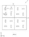
図3は、バックライト42用の例示的な発光ダイオードアレイの上面図である。図3に示すように、発光ダイオードアレイ36は、発光ダイオード38の行と列を含んでもよい。各発光ダイオード38は、それぞれのセル(タイル領域)38Cと関連付けられていてもよい。セル38Cの縁部の長さDは、2mm、18mm、1〜10mm、1〜4mm、10〜30mm、5mm超、10mm超、15mm超、20mm超、25mm未満、20mm未満、15mm未満、10mm未満、1mm未満、0.1mm未満、0.01mm超、0.1mm超、又は他の好適なサイズであってもよい。所望であれば、六角形状にタイル貼りされたアレイ及び、他の好適なアレイパターンで構成される発光ダイオード38を有するアレイが使用されてもよい。矩形セルを有するアレイでは、各セルが等しい長さの辺を有してもよく(例えば、各セルは、4つの等しい長さのセル縁部がそれぞれの発光ダイオードを取り囲む、正方形の外形線を有してもよい)、又は各セルが異なる長さの側部を有してもよい(例えば、正方形ではない矩形形状)。発光ダイオードアレイ36がセル38Cなどの正方形の発光ダイオード領域の行と列を有する図3の構成は、単なる例示である。 FIG. 3 is a top view of an exemplary light emitting diode array for the
所望であれば、各セル38Cは、発光ダイオードダイのアレイ(例えば、各セル38Cの中心に2×2個の発光ダイオードのクラスタなどのアレイで配置された複数の個別の発光ダイオード38)から形成された光源を有してもよい。例えば、図3の左下のセル38C内の光源38’は、2×2アレイの発光ダイオード38(例えば、4つの別個の発光ダイオードダイ)から形成されている。一般に、各セル38Cは、単一の発光ダイオード38、一対の発光ダイオード38、2〜10個の発光ダイオード38、少なくとも2つの発光ダイオード38、少なくとも4つの発光ダイオード38、少なくとも8つの発光ダイオード38、5つよりも少ない発光ダイオード38、又は他の好適な数の発光ダイオードを備える光源38’を含んでもよい。各セル38Cが単一の発光ダイオード38を有する例示的な構成が、本明細書では一例として記載される場合がある。しかし、これは単なる例示である。各セル38Cは、1つ以上の任意の好適な数の発光ダイオード38を有する光源38を有してもよい。発光ダイオードアレイ36内のダイオード38は、アレイ36にわたって延びるプリント回路基板上に実装されてもよく、又は他の適切な構成を使用してアレイ36内に実装されてもよい。 If desired, each
発光ダイオードアレイ36内の発光ダイオード38は、熱を発生させることがある。注意を怠ると、結果として生じる熱勾配(例えば、発光ダイオードに近いアレイの領域は、発光ダイオード間のアレイの領域よりも高温である)は、画素アレイ24内で熱勾配を引き起こすことがある。画素アレイ24によって放射される光の色は、温度に依存することがある。したがって、画素アレイ内の高い熱勾配は、ディスプレイ性能に悪影響を及ぼす可能性がある。 The
図4及び図5は、発光ダイオード38からの熱を分散させる(及び画素アレイ24内の熱勾配を防止する)のに役立つ層を有する例示的な発光ダイオードアレイの側断面図である。図4に示すように、発光ダイオード38は、導電性材料(例えば、半田)56を使用して、プリント回路基板50の導電性パッド54(例えば、半田パッド)に取り付けられてもよい。熱伝導層60は、接着剤層58を使用してプリント回路基板50の底面に取り付けられてもよい。接着剤層58は、負のZ方向(例えば、プリント回路基板50から)への熱を熱伝導層60に伝導することができる。次いで、熱伝導層60は、XY平面内で熱を分散させることができる。 4 and 5 are side sectional views of an exemplary light emitting diode array having layers that help disperse heat from the light emitting diode 38 (and prevent thermal gradients within the pixel array 24). As shown in FIG. 4, the
熱伝導層60は、任意の所望の材料から形成することができる。例えば、熱伝導層60は、アルミニウム、黒鉛、炭素繊維強化シート、カーボンナノチューブ、又は金属粒子から形成され得る。熱伝導層60は、200W/mK超、300W/mK超、400W/mK超、200W/mK〜400W/mKの熱伝導率、又は別の所望の熱伝導率を有してもよい。熱伝導層60は、0.1ミリメートル未満、0.2ミリメートル未満、約55マイクロメートル、20マイクロメートル超の厚さ62、又は別の所望の厚さを有してもよい。 The heat
接着剤層58は、感圧接着剤層であってもよい。所望であれば、接着剤層58は、接着剤層の熱伝導率を高めるために添加剤64(例えば、金属粒子)を含んでもよい。 The
別の実施形態では、図5に示すように、放射冷却コーティングをプリント回路基板50に取り付けてもよい。図5に示すように、層66(コーティング層、放射冷却層、又は放射冷却コーティングと呼ばれることもある)は、プリント回路基板50の底面に(例えば、接着剤58を使用して)取り付けられてもよい。層66は、ポリマーシートに埋め込まれた金属粒子を含んでもよい。金属粒子は、例えば、赤外光を放射し、それによって隣接する層を冷却することができる。 In another embodiment, the radiative cooling coating may be attached to the printed
図4及び図5に示すように、発光ダイオード38は、半田を使用してプリント回路基板50上の半田パッドに取り付けられる。半田と発光ダイオードとの間の重なり領域が少ない場合、半田と発光ダイオードとの間の結合の強度が低くなり得る。半田と発光ダイオードとの間の重なり領域(かつそれに応じて、接合強度及びSMT歩留まり)を増加させるために、発光ダイオードは、図6に示すように、矩形の設計を有してもよい。 As shown in FIGS. 4 and 5, the
図6は、矩形(正方形ではない)形状を有する例示的な発光ダイオードの上面図である。図に示すように、発光ダイオードアレイ36内の各発光ダイオードは、幅(W)、及びその幅よりも長い長さ(L)を有してもよい(例えば、その幅よりも長い、その幅の少なくとも2倍、その幅の長さの少なくとも1.5倍、その幅の少なくとも3倍、その幅の3倍未満など)。換言すれば、各発光ダイオードは、正方形ではない矩形形状を有してもよい。各セル(タイル領域)38Cは、関連する4つの発光ダイオード38−1、38−2、38−3、及び38−4を有することができる。図6に示すように、発光ダイオード38−1、38−2、38−3、及び38−4は、セル38C内の2×2グリッドに配置される。発光ダイオード38−1はグリッドの左上にあり、発光ダイオード38−2はグリッドの右上にあり、発光ダイオード38−3はグリッドの左下にあり、発光ダイオード38−3はグリッドの右下にある。発光ダイオード38−1及び38−4は、Y軸に平行な長さを有してもよく、発光ダイオード38−2及び38−3は、X軸に平行な(かつ38−1及び38−4の長さに対して90度回転された)長さを有してもよい。この構成では、各発光ダイオードは、(各タイル内の4つの発光ダイオードが均一なバックライトを一緒に発光するであろうから)均一なバックライトを確保しながら、(結合強度を高めるために)正方形ではない矩形輪郭を有し得る。各タイル内の発光ダイオードは、一緒に制御することができる。所与のセル内の各発光ダイオードは、任意の所望の位置決め及び向きを有することができる。所与のセル内の各発光ダイオードは、任意の所望の半田パターンを有することができる。所与のセル内の各発光ダイオードは、任意の所望の粒径及び分布の、任意の所望のカプセル材添加剤を有することができる。 FIG. 6 is a top view of an exemplary light emitting diode having a rectangular (not square) shape. As shown in the figure, each light emitting diode in the light emitting
発光ダイオードアレイ36内の発光ダイオードの別の構成を図7に示す。図7に示すように、各タイル38Cは、関連する複数(例えば、2つ、3つ、3つ超など)の発光ダイオードを有することができる。図7の例では、各タイル38Cは発光ダイオード38−1、38−2、及び38−3を含む。これらの発光ダイオードは、セルから放射される光を調整するのを助けるために、異なる特性を有してもよい。図7の実施例では、発光ダイオード38−2は発光ダイオード38−1よりも大きく、発光ダイオード38−1は発光ダイオード38−3よりも大きい。各発光ダイオードは、同じ又は異なるサイズを有してもよい。各発光ダイオードが正方形ではない矩形形状を有する図7の例は、単なる例示に過ぎず、各発光ダイオードは任意の所望の形状を有してもよい。別の可能な実施形態では、発光ダイオードは、異なるピーク波長の放射を有してもよい。加えて、図2に示すように、各発光ダイオードは、カプセル材52によって覆われてもよい。タイル38C内の各発光ダイオードは、異なる形状のカプセル材又は異なるドーパントを有するカプセル材によって覆われてもよい。 Another configuration of the light emitting diodes in the light emitting
一般に、所与のタイル内の複数の発光ダイオードは、そのタイルから放射される光を調整するために異なる特性を有し得る。これらの特性は、位置決め、向き、発光ダイオードに取り付けられた半田の特性、カプセル材添加剤の粒径、及びカプセル材添加剤の分布を含み得る。1つの例示的な実施例では、発光ダイオード38−1、38−2、及び38−3は、それぞれ赤色、青色、及び緑色発光ダイオードであってもよい(かつタイル38Cは白色光を放射する)。 In general, multiple light emitting diodes in a given tile may have different properties to regulate the light emitted from that tile. These properties may include positioning, orientation, properties of the solder attached to the light emitting diode, particle size of the capsule additive, and distribution of the capsule additive. In one exemplary embodiment, the light emitting diodes 38-1, 38-2, and 38-3 may be red, blue, and green light emitting diodes, respectively (and
図2は、発光ダイオードアレイ36内の発光ダイオード38からの光を拡散するために使用される光拡散層28を示す。図8は、プリント回路基板上に発光ダイオードに隣接する光方向転換層を有する、例示的な発光ダイオードアレイの側断面図である。図8に示すように、発光ダイオード38は、プリント回路基板50の上面に実装される。光方向転換層68もまた、プリント回路基板50の上面に実装される。光方向転換層68は、発光ダイオード38の縁部から放射された光を方向転換するのに役立つプリズム状反射体であってもよい。層68は、プリント回路基板50に積層された別個のフィルムであってもよく、又はプリント回路基板上のUV硬化性コーティング若しくは熱硬化性コーティング上にエンボス加工されてもよい。 FIG. 2 shows a
層68は、光学的な均一性及び効率を向上させるために、特定の方向に光をガイドするように設計することができる。層は、拡散、屈折、及び/又は回折光学特性を含むことができる。層68は、マイクロ構造体、パラボラ反射器、ある特定の波長を回折するエンボス構造体、又は画定された円錐角で光を放射するプリズム状構造体を含んでもよい。層68は、光拡散層28との組み合わせで作用してもよく、又は光拡散層28を置き換えてもよい。図8の実施例では、層68は、各隣接する発光ダイオード38間に2つの突出部を含む。
図9及び図10は、発光ダイオードアレイ36内の発光ダイオード38がどのように反射層を含み得るのか、又は含み得ないのかを示す側断面図である。図9に示すように、発光ダイオードは、発光ダイオード38からの放射光を横方向に向けるのを助けるために、反射層70(例えば、分散ブラッグ反射器)を含んでもよい。これにより、発光ダイオード38によって放射される光の軸上強度を低減することができる。しかしながら、これにより、プリント回路基板50の上面、半田パッド54及び半田56に当たる光の量が増加する。プリント回路基板50、半田パッド54及び半田56は、高反射率を有さない場合がある。したがって、反射層70の存在は、高い光損失をもたらし得る。光損失を低減するために、発光ダイオードは、(図10に示すように)反射層70を含まなくてもよい。 9 and 10 are side sectional views showing how the
図10は、半田厚さ及びプリント回路基板に対する発光ダイオードの対応する高さを低減し、発光ダイオードの下に封入される空気を低減することによって半田品質を向上する様々な方法を追加的に示す。図10に示すように、半田パッド54は、半田56の一部分を受け入れる凹部53B(例えば、半田パッドの上面内に)を有してもよい。毛管現象及び重力のため、凹部53Bによって、半田56を半田パッド54により良好に取り付けることができる。同様に、発光ダイオード38の下面は、半田56の一部分を受け入れる1つ以上の凹部53Aを有してもよい。再び、凹部53Aによって、半田56を発光ダイオード38により良好に取り付けることができる。所望であれば、1つ以上の凹部を導電性コーティングでコーティングしてもよい。 FIG. 10 additionally shows various ways to improve solder quality by reducing the solder thickness and the corresponding height of the light emitting diode with respect to the printed circuit board and reducing the air enclosed under the light emitting diode. .. As shown in FIG. 10, the
加えて、コーティング57は、発光ダイオード38の下のプリント回路基板50上に含まれてもよい。コーティング57は、誘電体(例えば、非導電性)コーティングであってもよい。コーティング57は疎水性であってもよく、半田56がコーティングを横切って流れることを可能にする。半田56が堆積されると、余分な半田は、コーティング57を横切ってプリント回路基板50の凹部55内に流れることができる。凹部55は、プリント回路基板50を部分的に通って延びてもよく、又は回路基板を通って完全に(例えば、上面から下面へ)通過してもよい。真空吸着を適用して(例えば、半田堆積中に)、ダイを整列させ、余分な空気を除去してもよい。説明したように、余分な半田を凹部55に流れさせることにより、半田品質及び配置の信頼性を向上し、ダイの傾きを低減し、ダイの下の空気を低減することができる。 In addition, the coating 57 may be included on the printed
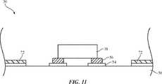
図11は、プリント回路基板及び他の隣接する層の反射率を増加させることによって、光損失を低減する方法を示す。図11に示すように、半田マスク72(半田マスク反射器又は反射層と呼ばれることもある)は、発光ダイオードアレイ36に含まれてもよい。半田マスク72は、発光ダイオード38からの光が半田マスク72に当たるときの損失を低減するために、高反射材料から形成されてもよい。半田マスクは、反射率を増加させるために、二酸化チタン(TiO2)(例えば、ポリマー中に分散された二酸化チタン粒子)又は他の所望の材料を含んでもよい。半田マスク内の二酸化チタンの粒径、並びにポリマーの屈折率は、反射率を最適化するように調整されてもよい。一実施形態では、半田マスクは、プリント回路基板の上面に直接積層されてもよい。別の実施形態では、半田マスクは、熱硬化性コーティング又は紫外線硬化性コーティングであってもよい。半田マスクは、任意の所望の厚さ(例えば、50マイクロメートル、50マイクロメートル超、100マイクロメートル未満、50マイクロメートル未満など)を有してもよい。FIG. 11 shows a method of reducing light loss by increasing the reflectance of the printed circuit board and other adjacent layers. As shown in FIG. 11, the solder mask 72 (sometimes referred to as a solder mask reflector or reflective layer) may be included in the light emitting
プリント回路基板50の特性はまた、高反射率のために最適化されてもよい。例えば、ガラス繊維材料又は白色ポリイミドポリマーは、プリント回路基板50のコアを形成してもよい。半田マスク及びプリント回路基板の反射率は、同じであってもよく、又は異なっていてもよい(例えば、80%超、50%超、90%超、92%超、94%超、85%〜95%、90%未満、99%未満、80%〜95%など)。熱伝導性充填剤はまた、プリント回路基板50に加えられて、プリント回路基板の熱伝導率を調整することができる。 The properties of the printed
プリント回路基板50上の発光ダイオードをカプセル化する(例えば、これに適合する)カプセル材のための多数の可能な実施形態が存在する。図12は、平坦な上面を有するカプセル材52を有する例示的な発光ダイオードアレイの側断面図である。図12に示すように、カプセル材52は、発光ダイオードの上に延びる平坦な上面74を有してもよい。カプセル材52(この実施形態ではカプセル材のスラブと呼ばれることもある)は、発光ダイオード38のための更なる構造完全性を提供する。加えて、カプセル材52と隣接材料76(例えば空気)との間の界面で発光ダイオード38から放射される光の内部全反射を低減するために、カプセル材52は、発光ダイオード38の屈折率と材料76の屈折率との間にある屈折率を有することができる。例えば、カプセル材52は、1.2〜1.5、1.3〜1.4、1.4未満、1.5未満、1.1超、1.2超、1.3超、約1.35などの屈折率を有してもよい。図12に示すカプセル材52のスラブは、発光ダイオードアレイ36内の全ての発光ダイオードを覆うことができる。カプセル材52は、任意の所望の厚さ78(例えば、0.1ミリメートル〜0.4ミリメートル、0.5ミリメートル未満、0.3ミリメートル未満、0.2ミリメートル〜0.4ミリメートル、0.15ミリメートル〜0.25ミリメートル、0.25ミリメートル〜0.35ミリメートル、約0.2ミリメートル、約0.3ミリメートルなど)を有してもよい。 There are a number of possible embodiments for encapsulation materials that encapsulate (eg, fit) the light emitting diodes on the printed
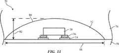
図13は、曲面の上面を有するカプセル材52を有する例示的な発光ダイオードアレイの側断面図である。図13に示すように、カプセル材52は、曲面の上面80(例えば、凸状の上面)を有してもよい。カプセル材は、発光ダイオードの上にドーム形状を形成してもよい。そのような実施形態では、カプセル材は、液滴レンズと呼ばれることもある。カプセル材52は、発光ダイオード38に更なる構造完全性を提供する。加えて、カプセル材52と隣接材料76(例えば空気)との間の界面で発光ダイオード38から放射される光の内部全反射を低減するために、カプセル材52は、発光ダイオード38の屈折率と材料76の屈折率との間にある屈折率を有することができる。例えば、カプセル材52は、1.2〜1.5、1.3〜1.4、1.4未満、1.5未満、1.1超、1.2超、1.3超、約1.35などの屈折率を有してもよい。各発光ダイオードは、対応するカプセル材部分(例えば、各発光ダイオードに対して1つのカプセル材のドーム)を有してもよい。カプセル材52は、任意の所望の厚さ82(例えば、0.1〜0.4ミリメートル、0.5ミリメートル未満、0.3ミリメートル未満、0.2〜0.4ミリメートル、0.15〜0.25ミリメートル、0.25ミリメートル〜0.35ミリメートル、約0.2ミリメートル、約0.3ミリメートルなど)、及び任意の所望の幅84(例えば、0.3〜2.5ミリメートル、0.3〜0.7ミリメートル、0.8〜0.9ミリメートル、0.5ミリメートル超、1.0ミリメートル超、2.0ミリメートル超、2.0ミリメートル未満など)を有してもよい。幅対厚さの比は、5対1超、3対1超、4対1〜6対1、10対1未満などであってもよい。 FIG. 13 is a side sectional view of an exemplary light emitting diode array having a
図14は、曲面の上面及び凹部を有するカプセル材52を有する例示的な発光ダイオードアレイの側断面図である。図14のカプセル材は、図13のカプセル材(例えば、ドーム形状を有する)と類似である。しかしながら、図14では、追加のカプセル材52は、発光ダイオード38の上に形成された凹部86を有する。凹部86はまた、ディップ(dip)と呼ばれることもある。凹部86は、任意の所望の形状(例えば、ピラミッド形状)を有してもよい。凹部86は、軸上(例えば、ゼロオーダー)の光の強度を低減することによって、図13の実施形態(凹部を有さない)と比較して、均一性を更に増加させることができる。 FIG. 14 is a side sectional view of an exemplary light emitting diode array having a curved top surface and a
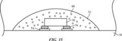
図15〜図17は、カプセル材52に含まれるドーパントの例を示す。図15は、ドーパント88を含むカプセル材52によって覆われた発光ダイオード38を示す側断面図である。ドーパント88(添加剤88と呼ばれることもある)は、散乱ドーパント(scattering dopant)であってもよい。ドーパント88の存在によって、発光ダイオード38の発光領域を増加させることができる。散乱ドーパントがないと、発光ダイオード38から放射された光は、発光ダイオード38の真上に集中する。しかしながら、散乱ドーパントによって、発光ダイオード38からの光をカプセル材52全体に拡散させることができる。したがって、カプセル材52の全領域が、発光ダイオード38からの光を放射する。この光の拡散は、例えば、図2の光拡散層28との組み合わせで作用してもよく、又は光拡散層28を置き換えてもよい。 15 to 17 show examples of dopants contained in the
任意の所望のドーパントをドーパント88に使用することができる。例えば、ドーパント88は、ポリマーナノ粒子、無機ナノ粒子、空隙(例えば、気泡)、又は任意の他の所望のドーパントを含んでもよい。カプセル化52内のドーパントの分布は、カプセル化材料(例えば、カプセル化樹脂)中のドーパントの浮力を介して制御することができる。例えば、図15は、中立の浮力の例を示す。したがって、図15のドーパント88は、カプセル化52全体にわたって均一に分散される(例えば、ドーパントは、カプセル化材料内のどこにでも浮遊させることができる)。図16は、ドーパント88が高い浮力を有し、したがって、カプセル材の上面に沿って分散する傾向がある(例えば、ドーパントがカプセル材の上部に浮遊するため)例を示す。対照的に、図17は、ドーパント88が低い浮力を有し、したがって、カプセル材の下面に沿って分布する傾向がある(例えば、ドーパントがカプセル材の底部に沈むため)例を示す。 Any desired dopant can be used for the
所望であれば、ドーパント88の場所を制御してもよい。例えば、ドーパントは、発光ダイオード38の上部に直接配置されてもよい。ドーパント88はまた、カプセル材52内のドーパント88の向きを制御することができるように設計されてもよい。一実施例では、図18に示すように、ドーパント88(例えば、特定の粒子)は、2つの異なる密度を有する2つの部分を有してもよい。図18に示すように、ドーパント88は、部分88−1及び部分88−2を含んでもよい。部分88−2は、部分88−1とは異なる密度(例えば、より高い)を有し得る。別の実施例では、図19に示すように、ドーパント88の形状は、ドーパント88の向きを制御するように設計されてもよい。図19に示す形状(マッシュルーム形状と呼ばれることもある)によって、カプセル材52内のドーパント88の向きを制御することができる。 If desired, the location of the
ドーム形状のカプセル材領域内のドーパント88を示す前述の実施例は、単なる例示に過ぎない。一般に、任意の所望のカプセル材(例えば、図12のような平坦な上面又は図14のような凹部分を有するカプセル材)は、ドーパントを含んでもよい。 The above-mentioned embodiment showing the
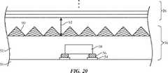
図20は、発光ダイオードアレイ36がカプセル化52上にパターン化層90を含み得る様子を示す、例示的なバックライトユニットの側断面図である。パターン化層90は、発光ダイオード38からの光の拡散に役立ち得る(例えば、図2の光拡散層28との組み合わせで作用する、又は光拡散層28を置き換える)。パターン化層90はまた、光学フィルム26とカプセル材52との間のギャップ92(例えば、エアギャップ)を維持するのに役立ち得る。パターン化層90は、カプセル材52の上面に取り付けられた別個のフィルムであってもよい。代わりに、パターン化層90は、カプセル材料のパターン化された部分から形成されてもよい(例えば、パターン化層90はカプセル材52の一部であってもよい)。 FIG. 20 is a side sectional view of an exemplary backlight unit showing how the light emitting
図21は、発光ダイオードアレイ36がテクスチャ加工された表面を有するカプセル化52を含み得る様子を示す例示的なバックライトユニットの側断面図である。図21に示すように、カプセル化52は、テクスチャ加工された上面94を有する。テクスチャ加工された上面94は、概ね平坦であってもよい(例えば、カプセル化はスラブとして形成される)。しかしながら、上面は粗くてもよい(滑らかではなく)。テクスチャ加工された上面は、発光ダイオード38から放射された光の内部全反射を防止し、効率を高めることができる。上面のテクスチャは不規則であってもよい。 FIG. 21 is a side sectional view of an exemplary backlight unit showing how the light emitting
バックライトユニットにおけるプリント回路基板の反射率を増加させるために、反射層を使用してもよい。例えば、反射材料は、プリント回路基板上に積層されてもよい。しかしながら、反射材料が半田リフロー中に損傷しないように注意しなければならない。反射材料は、半田の融点以下の融点を有する場合がある。したがって、半田をリフローすると、反射材料を融解(及び損傷)することがある。 A reflective layer may be used to increase the reflectance of the printed circuit board in the backlight unit. For example, the reflective material may be laminated on a printed circuit board. However, care must be taken to ensure that the reflective material is not damaged during solder reflow. The reflective material may have a melting point below that of the solder. Therefore, reflowing solder can melt (and damage) the reflective material.
反射層の損傷を防止するために、反射層は、半田リフロー後に回路基板に積層されてもよい。代わりに、反射層は、半田リフロー前にプリント回路基板に取り付けられてもよい。次いで、半田マスクを使用して、半田リフロー中に反射層を損傷から保護することができる。このタイプの構成を図22に示す。 In order to prevent damage to the reflective layer, the reflective layer may be laminated on the circuit board after solder reflow. Alternatively, the reflective layer may be attached to the printed circuit board prior to solder reflow. A solder mask can then be used to protect the reflective layer from damage during solder reflow. This type of configuration is shown in FIG.
図22に示すように、反射層96は、プリント回路基板50上に(例えば、プリント回路基板50の上面上に)形成することができる。反射層は、任意の所望の材料から形成することができる。反射層は、1つ以上の層から形成することができる。反射層は、発光ダイオードによって放射される波長における光の高反射率を有し得る。例えば、発光ダイオードが青色光を放射する場合、反射層96は、青色光の高反射率(例えば、80%超、90%超、92%超、94%超、96%超、99%未満など)を有することができる。半田56はまた、プリント回路基板50上に(例えば、反射層で覆われていないことがあるプリント回路基板の上面上の導電性パッド上に)形成されてもよい。熱源100を使用して、リフローのために半田56を加熱することができる。熱源100は、半田マスク98を通してエネルギ(例えば、赤外光)を放射することによって、半田96を加熱することができる。半田マスク98は、半田56と重なり合う開口部を有してもよい。半田56で覆われていないプリント回路基板50の部分は、半田マスク98によって覆われ得る。このようにして、半田マスク98は、半田56の加熱中に反射層96が損傷するのを防ぐことができる。半田マスク98は、不透明であるか、又は熱源100によって放射されるエネルギ(102)に対して耐性のある任意の材料から形成することができる。熱源100は、例えば、赤外光を放射するレーザーであってもよい。 As shown in FIG. 22, the
特定の実施形態では、バックライトユニット42は、発光ダイオード38によって放射される光の点像分布関数(Point Spread Function、PSF)幅を増大させるのに役立つ偏光回折格子を含んでもよい。PSF幅を増大させることにより、再利用のためのプリント回路基板の反射率への依存を低減することができる。図23〜図25は、偏光回折格子層(回析層、光拡散層、偏光位相格子層、偏光格子、又は偏光位相格子と呼ばれることもある)を有する例示的なバックライトユニットの側断面図である。図23に示すように、バックライトユニット42は、カプセル化52によって覆われたプリント回路基板50上の発光ダイオード38を含む。バックライトユニットはまた、光拡散層28を含む光学フィルム26を有してもよい。しかしながら、バックライトユニットは、追加的な光拡散層104を含んでもよい。偏光回折格子層104(回析層、光拡散層、偏光位相格子層、偏光格子、又は偏光位相格子と呼ばれることもある)は、発光ダイオード38から受光した光を2つの異なる偏光に分割することができる。光拡散層104は、発光ダイオードに関連付けられた軸上の強度ピークを低減することができる。 In certain embodiments, the
図23に示すように、光拡散層104は、発光ダイオードを覆うカプセル化52に結合されてもよい(例えば、光拡散層104は、カプセル化52に直接接触してもよい)。この例は単なる例示に過ぎない。図24に示す別の例では、光拡散層104は、光拡散層28の下面上に形成される。光拡散層28及び光拡散層104は、任意の所望の方法で一緒に取り付けられてもよい。光拡散層28は、光拡散層の上面上に均一にパターン化された突出部を有してもよい。更に別の実施形態では、図25に示すように、導波路層106(導光層と呼ばれることもある)は、光拡散層28と光拡散層104との間に介在してもよい。光拡散層28は、この実施形態では、光拡散層の上面上に不均一に離隔された(例えば、導波路の拡散を制御するために統計的に離隔された)突出部を有してもよい。 As shown in FIG. 23, the
他の構造を使用して、発光ダイオード38によって放射される光の点像分布関数(PSF)幅を増加させてもよい。図26及び図27は、高反射性プリント回路基板との組み合わせで発光ダイオード38によって放射される光の点像分布関数(PSF)幅を増加させる構造体を含むバックライトユニットの側断面図である。図26に示すように、発光ダイオード38は、プリント回路基板50上に位置決めされてもよく、カプセル材52によって覆われてもよい。各発光ダイオード38は、それぞれの放物線状の上面108を有するカプセル材のそれぞれの部分によって覆われてもよい。隣接するカプセル材部分の放物線状の上面は、頂点110で交わってもよい。この部分は、カプセル材52のくぼみ又は凹部分と呼ばれることもある。 Other structures may be used to increase the point spread function (PSF) width of the light emitted by the
発光ダイオード38から放射された光112は、内部全反射(TIR)によって頂点110に向かって反射され得る。光112が頂点110(光漏出促進構造体110と呼ばれることもある)に到達すると、光は、観察者の方向にカプセル材52から出ていく可能性が高くなり得る。このようにして、発光ダイオードからの光は、隣接する発光ダイオード間の領域に向けられ、そこから放射されてもよい(それによって、PSF幅を増大させる)。このタイプの構成は、プリント回路基板50で反射する光に依存する(例えば、光は発光ダイオードから放射され、内部全反射によりカプセル材の放物線状の上面で反射し、次いで、プリント回路基板の上面で反射する)。したがって、プリント回路基板の反射率が低い場合、図26の構成を有するバックライトユニットの効率が低くなり得る。したがって、図26の構成は、プリント回路基板が高反射率(例えば、90%超、94%超、96%超など)を有する実施形態に好適であり得る。 The light 112 emitted from the
別の実施形態では、図27に示すように、発光ダイオード38は再びプリント回路基板50上に位置決めされ、カプセル材52によって覆われてもよい。この実施形態では、発光ダイオードは、平坦な上面を有するカプセル材によって覆われている(例えば、カプセル材のスラブ)。光漏出促進構造体114は、各発光ダイオード間に介在していてもよい。図27の光漏出促進構造体114は、不透明な白色構造体から形成されてもよい。別の実施形態では、光漏出促進構造体114は、カプセル材52内のエアギャップ(空隙と呼ばれることもある)であってもよい。 In another embodiment, as shown in FIG. 27, the
発光ダイオード38から放射された光は、内部全反射(TIR)によって光漏出促進構造体114に向かって反射され得る。光が光漏出促進構造体114に到達すると、光は、観察者の方向にカプセル材52から出ていく可能性が高くなり得る。このようにして、発光ダイオードからの光は、隣接する発光ダイオード間の領域に向けられ、そこから放射されてもよい(それによって、PSF幅を増大させる)。このタイプの構成は、プリント回路基板50で反射する光に依存する(例えば、光は、発光ダイオードから放射され、内部全反射によりカプセル材の上面で反射し、次いで、プリント回路基板の上面で反射する)。したがって、図27の構成は、プリント回路基板が高反射率(例えば、90%超、94%超、96%超など)を有する実施形態に好適であり得る。 The light emitted from the
光を拡散するための光拡散層28(例えば、図2に示す)の多くの可能な方法が存在する。図28は、上面及び下面の両方にマイクロレンズ構造を有する光拡散層を有する例示的なディスプレイの側断面図である。図28に示すように、光拡散層28は、上面116及び下面118を有する。上面116は、光拡散層の上面内の凹部から形成された複数のマイクロレンズ120を有する。マイクロレンズ120は、上面116内における球状形状の凹部又は任意の他の所望の形状の凹部から形成されてもよい。下面118はまた、光拡散層の下面内の凹部から形成された複数のマイクロレンズ122を有する。マイクロレンズ122は、下面118内における球状形状の凹部又は任意の他の所望の形状の凹部から形成されてもよい。マイクロレンズ122は、(図28に示すように)マイクロレンズ120よりも大きくてもよい。しかしながら、この例は単なる例示に過ぎず、マイクロレンズ122はまた、マイクロレンズ120と同一サイズであっても、又は小さくてもよい。加えて、マイクロレンズアレイ120内の各マイクロレンズは、同一サイズ又は異なるサイズを有してもよく、マイクロレンズアレイ122内の各マイクロレンズは、同一サイズ又は異なるサイズを有してもよい。 There are many possible methods of light diffusing layer 28 (eg, shown in FIG. 2) for diffusing light. FIG. 28 is a side sectional view of an exemplary display having a light diffusing layer having a microlens structure on both the top and bottom surfaces. As shown in FIG. 28, the
光拡散層28の別の構成を図29に示す。図29に示すように、光拡散層は、2つのフィルム(層)を含んでもよい。図29の実施例では、光拡散層28−1は、光拡散層28−2の上方に配置される。光拡散層28−1及び光拡散層28−2は、例えば、接着剤128(例えば、感圧接着剤)を使用して取り付けることができる。所望であれば、接着剤128は、拡散特性を有してもよい。 Another configuration of the
図29に示すように、光拡散層28−2は、マイクロレンズ132を有する上面を有する。マイクロレンズ132は、光拡散層28−2の上面内の複数の凹部から形成されてもよい。光拡散層28−2はまた、複数の突出部130を含んでもよい。突出部130は、発光ダイオードに向かって突出してもよい。突出部130は、層にわたって長手方向軸に沿って延在する細長い突出部(隆起部と呼ばれることもある)であってもよい(例えば、図29のY軸に平行)。光拡散層28−1は、光拡散層28−2に対して90度回転されていることを除いて、光拡散層28−2と同じであってもよい。例えば、光拡散層28−1はまた、層にわたって長手方向軸に沿って延びる複数の突出部を有する。しかしながら、光拡散層28−1の突出部は、X軸(光拡散層28−2の突出部に対して垂直)に平行に延びてもよい。光拡散層28−1はまた、マイクロレンズ126を含む。マイクロレンズ126は、光拡散層28−1の上面124内の複数の凹部から形成されてもよい。 As shown in FIG. 29, the light diffusing layer 28-2 has an upper surface having a
発光ダイオード38から放射された光は、光拡散層28−2に到達すると、第1の軸に対して(例えば、点光源から2点に)拡散する。マイクロレンズ132は、内部全反射を低減して、光拡散層28−1への光の通過を促進することができる。光拡散層28−1は、第1の軸に垂直な第2の軸(例えば、2点から4点)に対して入射光を拡散する(層28−1の突出部が層28−2の突出部に対して垂直であるため)。マイクロレンズ126は、内部全反射を低減して、層28−1から層30に向かう光の漏出を促進することができる。層28−1及び28−2はそれぞれ、任意の所望の厚さ(例えば、20〜30マイクロメートル、20〜25マイクロメートル、50マイクロメートル未満、25マイクロメートル未満、約22マイクロメートル、15マイクロメートル超、100マイクロメートル未満など)を有してもよい。層28−1及び28−2の厚さは同じであってもよい。 When the light emitted from the
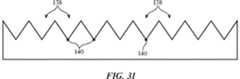
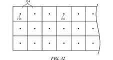
長手方向軸に沿って延びる(かつ入射する点光源を2点に分割する)細長い突出部を有する光拡散層28の例は、単に例示に過ぎない。所望であれば、光拡散層28は、代わりに、突出部又は凹部のアレイを含んでもよい。各突出部は、入射する点光源を3点以上に分割することができる。図30は、突出部134を含む光拡散層28の側断面図である。突出部134は、任意の所望の形状を有してもよい。例えば、突出部は、角錐形状(例えば、正方形の底面と頂点136で交わる4つの三角形の面を有する)であってもよく、又は三角錐形状(例えば、三角形の底面と頂点136で交わる3つの三角形の面を有する)であってもよい。角錐状突出部は、点光源を4点に分割することができるのに対して、三角錐状突出部は、点光源を3点に分割することができる。別の実施形態では、図31に示すように、光拡散層28は、複数の凹部138を含んでもよい。凹部138は、任意の所望の形状を有してもよい。例えば、凹部は、角錐形状(例えば、正方形の底面と頂点140で交わる4つの三角形の面を有する)であってもよく、又は三角錐形状(例えば、三角形の底面と頂点140で交わる3つの三角形の面を有する)であってもよい。角錐状の凹部は、点光源を4つの点に分割することができるのに対して、三角錐状の凹部は、点光源を3つの点に分割することができる。図32は、突出部134(又は凹部138)がどのようなアレイ状に配置され得るかを示す光拡散層28の上面図である。突出部及び/又は凹部は、任意の所望の形状を有してもよく、任意の所望のタイプのアレイに配置されてもよい。 The example of the
図33は、部分キューブ構造(コーナキューブと呼ばれることもある)から形成された突出部134を有する光拡散層の上面図である。図に示すように、各突出部(又は凹部)は、頂点136で交わる3つの正方形の面(例えば、コーナーキューブ)によって形成されてもよい。図34では、各突出部134は、互いにオフセットされた2つの部分キューブ構造から形成されている。したがって、図34の各突出部134は、6つの面を有する(かつ入射する点光源を6点に分割する)。 FIG. 33 is a top view of a light diffusing
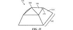
図35に示す更に別の実施形態では、突出部134は、テーパ状角錐構造から形成されてもよい。図35に示すように、突出部は、頂点148で交わる4つの面142を有することができる。各面は、互いに対して角度150である下部144及び上部146を有することができる。角度150は、光拡散層の光拡散機能を最適化するように選択することができる。 In yet another embodiment shown in FIG. 35, the
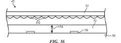
発光ダイオード38からの光を拡散するための追加の実施形態を、図36〜図39に示す。図36は、部分的反射層30の下面上に形成されたマイクロレンズアレイを有する例示的なバックライトユニットの側断面図である。マイクロレンズ152は、部分的反射層30の下面から突出してもよい。マイクロレンズは、発光ダイオード38から受光した光を拡散させるのに役立ち得る。マイクロレンズ152は、関連する焦点距離(f)を有してもよい。カプセル材52の厚さ154は、焦点距離(例えば、t=n×f、ここで、tは厚さ154であり、nはカプセル材料の屈折率である)の関数であってもよい。 Additional embodiments for diffusing the light from the
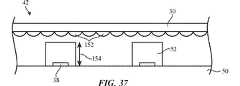
図37は、図36と類似の構成を示す。しかしながら、図36では、カプセル材52は、アレイ内の発光ダイオードの全てにわたって形成される(例えば、カプセル材スラブ)。図37では、各発光ダイオードは、カプセル材52のそれぞれの部分を有する。図37では、各カプセル材部分の厚さ154は、マイクロレンズ152の焦点距離及びカプセル材料の屈折率に基づいて選択されてもよい。 FIG. 37 shows a configuration similar to that of FIG. 36. However, in FIG. 36, the
図38は、部分的反射層30の下面上にマイクロレンズ152を有する更に別の実施形態を示す。図38では、各発光ダイオードは、(図37のような平坦な上面の代わりに)曲面の上面を有するカプセル材部分52によって覆われてもよい。図38では、各カプセル材部分の厚さ154は、マイクロレンズ152の焦点距離(例えば、t=f、ここで、tは厚さ154であり、fはマイクロレンズ152の焦点距離である)に基づいて選択されてもよい。 FIG. 38 shows yet another embodiment having a
部分的反射層30の下面に形成されているマイクロレンズ152の図36〜図38の例は、単なる例示に過ぎない。所望であれば、マイクロレンズ152は、ディスプレイ内の他の場所に形成されてもよい。図39は、マイクロレンズ152が基板156上に形成されている(部分的反射層30から分離している)実施形態を示す。発光ダイオード38とマイクロレンズ152用の基板156との間に、エアギャップ158が存在してもよい。 The examples of FIGS. 36 to 38 of the
図36〜図39に示す実施形態では、光拡散層28は省略されている(マイクロレンズ152が発光ダイオードからの光を拡散するため)。しかしながら、これは単なる例示に過ぎない。所望であれば、光拡散層28は、図36〜図39の実施形態のいずれかに含まれてもよい(及び、マイクロレンズ152との組み合わせで光を拡散する)。 In the embodiments shown in FIGS. 36 to 39, the
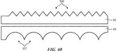
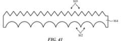
図2は、バックライトユニット42が輝度向上フィルム46及びコリメート層44を含む実施例を示した。これらの層の例を、再び図40に示す。図40に示すように、輝度向上フィルム46は、フィルムの上面に突出部160を含んでもよい。コリメート層44は、フィルムの下面上にマイクロレンズ162のアレイを含んでもよい。バックライトユニット42内の層数を低減するために、輝度向上フィルム46及びコリメート層44は、単一のフィルムに結合されてもよい。図41は、上面上に突出部160(輝度向上フィルムの機能を果たす)、及び下面上にマイクロレンズ162(コリメート層の機能を果たす)を有する例示的な光学層164の側断面図である。 FIG. 2 shows an example in which the
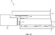
光学フィルム26の縁部からの光の漏出は、ディスプレイの縁部に望ましくない青色の色合いを生じさせることがある(画素アレイ24が発光ダイオード38から過剰な青色光を受光することによる)。この問題を軽減するために、ディスプレイの縁部に1つ以上のコーティングが含まれてもよい。図42に示すように、ディスプレイ14は、画素アレイ24の下層にコーティング168を含むことができる。ディスプレイは、ディスプレイ14内の1つ以上の他の層を支持するシャーシ166(例えば、Pシャーシと呼ばれることもあるプラスチックシャーシ)を含んでもよい。シャーシの1つ以上の表面(例えば、縁部表面176)は、コーティング174によってコーティングされる。光学層の上面は、コーティング170でコーティングされる。光学層の縁部表面は、コーティング172でコーティングされる。コーティング168、170、172及び174(全てディスプレイの縁部にある)は、黒色材料、灰色材料、黄色材料、又は蛍光体材料から形成されてもよい。黒色材料、灰色材料、及び黄色材料は、青色光の反射率を調節又は除去することができる(それによって、ディスプレイの縁部における過剰な青色光を低減する)。蛍光体材料は、青色光を白色光に変換することができる(それによって、ディスプレイの縁部における過剰な青色光を低減する)。 Leakage of light from the edges of the
一実施形態によれば、複数の画素と、複数の画素に対してバックライト照明を生成するように構成されたバックライトであって、光を放射するように構成され、複数のそれぞれのセル内に配置された光源と、光源から光を受光し、第1の方向に延びる第1の複数の細長い突出部を有する第1の光拡散層と、第1の光拡散層から光を受光し、第1の方向に垂直な第2の方向に延びる第2の複数の細長い突出部を有する第2の光拡散層と、を含む、バックライトと、を含む、ディスプレイが提供される。 According to one embodiment, a plurality of pixels and a backlight configured to generate backlight illumination for the plurality of pixels, configured to radiate light and within each of the plurality of cells. A light source arranged in the light source, a first light diffusing layer having a first plurality of elongated protrusions extending in a first direction and receiving light from the light source, and a light diffusing layer receiving light from the first light diffusing layer. A display is provided that includes a backlight, including a second light diffusing layer having a second plurality of elongated protrusions extending in a second direction perpendicular to the first direction.
別の実施形態によれば、光源は、プリント回路基板上に実装された発光ダイオードを含む。 According to another embodiment, the light source includes a light emitting diode mounted on a printed circuit board.
別の実施形態によれば、バックライトは、プリント回路基板の下面に接着剤で取り付けられた熱伝導層を含む。 According to another embodiment, the backlight comprises a heat conductive layer adhesively attached to the underside of the printed circuit board.
別の実施形態によれば、接着剤は、熱伝導性添加剤を含む。 According to another embodiment, the adhesive comprises a thermally conductive additive.
別の実施形態によれば、バックライトは、プリント回路基板の下面上に放射冷却コーティングを含む。 According to another embodiment, the backlight comprises a radiative cooling coating on the underside of the printed circuit board.
別の実施形態によれば、バックライトは、発光ダイオードの上に形成された平坦な上面を有するカプセル材の層を含む。 According to another embodiment, the backlight comprises a layer of capsule material having a flat top surface formed on top of the light emitting diode.
別の実施形態によれば、バックライトはカプセル材を含み、各発光ダイオードは、曲面の上面を有するそれぞれのカプセル材部分によって覆われている。 According to another embodiment, the backlight comprises a capsule material, and each light emitting diode is covered with a respective capsule material portion having a curved upper surface.
別の実施形態によれば、それぞれの各カプセル材部分の曲面の上面は、発光ダイオードの上にそれぞれの凹部を有する。 According to another embodiment, the upper surface of the curved surface of each capsule material portion has its own recess above the light emitting diode.
別の実施形態によれば、バックライトは、発光ダイオードの上に形成され、かつ散乱ドーパントを含むカプセル材の層を含む。 According to another embodiment, the backlight comprises a layer of encapsulant formed on the light emitting diode and containing a scattering dopant.
別の実施形態によれば、バックライトはカプセル材を含み、各発光ダイオードは、放物線状の上面を有するそれぞれのカプセル材部分によって覆われている。 According to another embodiment, the backlight comprises a capsule material and each light emitting diode is covered by a portion of the capsule material having a parabolic top surface.
別の実施形態によれば、バックライトは、隣接する発光ダイオード間に介在する光漏出促進構造体を含む。 According to another embodiment, the backlight comprises a light leakage promoting structure interposed between adjacent light emitting diodes.
別の実施形態によれば、それぞれの各セルは、正方形ではない矩形形状を有する4つの発光ダイオードを含む。 According to another embodiment, each cell comprises four light emitting diodes having a rectangular shape rather than a square shape.
別の実施形態によれば、それぞれの各セルは、第1のサイズを有する第1の発光ダイオードと、第1のサイズとは異なる第2のサイズを有する第2の発光ダイオードと、を含む。 According to another embodiment, each cell comprises a first light emitting diode having a first size and a second light emitting diode having a second size different from the first size.
別の実施形態によれば、それぞれの各セルは、赤色発光ダイオードと、青色発光ダイオードと、緑色発光ダイオードと、を含む。 According to another embodiment, each cell comprises a red light emitting diode, a blue light emitting diode, and a green light emitting diode.
別の実施形態によれば、第1の複数の細長い突出部は第1の光拡散層の下面から延びており、第1の光拡散層は、第1の光拡散層の上面上に形成されたマイクロレンズの第1のアレイを有し、第2の複数の細長い突出部は第2の光拡散層の下面から延びており、第2の光拡散層は、第2の光拡散層の上面上に形成されたマイクロレンズの第2のアレイを有する。 According to another embodiment, the first plurality of elongated protrusions extend from the lower surface of the first light diffusing layer, and the first light diffusing layer is formed on the upper surface of the first light diffusing layer. It has a first array of microlenses, a second plurality of elongated protrusions extending from the lower surface of the second light diffusing layer, the second light diffusing layer being the upper surface of the second light diffusing layer. It has a second array of microlenses formed on top.
一実施形態によれば、複数の画素と、複数の画素に対してバックライト照明を生成するように構成されたバックライトであって、プリント回路基板と、プリント回路基板上に実装された複数の発光ダイオードと、複数の発光ダイオードから受光した光を拡散するプリント回路基板の上に形成された少なくとも1つの光拡散層と、少なくとも1つの光拡散層の上に形成された部分的反射層と、部分的反射層の上に形成された色変換層と、色変換層の上に形成されたコリメート層と、を含む、バックライトと、を含む、ディスプレイが提供される。 According to one embodiment, a plurality of pixels and a plurality of backlights configured to generate backlight illumination for the plurality of pixels, the printed circuit board and a plurality of mounted on the printed circuit board. A light-emitting diode, at least one light-diffusing layer formed on a printed circuit board that diffuses light received from a plurality of light-emitting diodes, and a partial reflection layer formed on at least one light-diffusing layer. A display is provided that includes a backlight, including a color conversion layer formed on top of a partially reflective layer and a collimating layer formed on top of the color conversion layer.
別の実施形態によれば、色変換層は、更なる部分的反射層の上に形成された蛍光体層を含む。 According to another embodiment, the color conversion layer includes a phosphor layer formed on top of an additional partially reflective layer.
別の実施形態によれば、少なくとも1つの光拡散層は、複数の発光ダイオードから光を受光し、第1の方向に延びる第1の複数の細長い突出部を有する第1の光拡散層と、第1の光拡散層から光を受光し、第1の方向に垂直な第2の方向に延びる第2の複数の細長い突出部を有する第2の光拡散層と、を含む。 According to another embodiment, the at least one light diffusing layer receives light from the plurality of light emitting diodes and has a first light diffusing layer having a plurality of elongated protrusions extending in a first direction. It includes a second light diffusing layer that receives light from the first light diffusing layer and has a second plurality of elongated protrusions extending in a second direction perpendicular to the first direction.
一実施形態によれば、複数の画素と、複数の画素に対してバックライト照明を生成するように構成されたバックライトであって、光を放射する複数の発光ダイオードを含む発光ダイオードアレイと、発光ダイオードアレイの上に形成された複数の光学フィルムと、複数の発光ダイオードによって放射された光を受光し、光の色を変化させる複数の光学フィルムの縁部に形成されたコーティングと、を含む、バックライトと、を含む、ディスプレイが提供される。 According to one embodiment, a light emitting diode array comprising a plurality of pixels and a plurality of light emitting diodes that are configured to generate backlight illumination for the plurality of pixels and emit light. Includes a plurality of optical films formed on a light emitting diode array and a coating formed on the edges of the plurality of optical films that receive the light emitted by the light emitting diodes and change the color of the light. , Backlit, and displays are provided.
別の実施形態によれば、コーティングは、黒色材料、灰色材料、黄色材料、又は蛍光体材料からなる群から選択されるコーティングを含む。 According to another embodiment, the coating comprises a coating selected from the group consisting of black material, gray material, yellow material, or phosphor material.
前述は、単なる例示に過ぎず、説明された実施形態に対して多様な変更を行うことができる。前述の実施形態は、個別に又は任意の組み合わせで実装することができる。 The above is merely an example, and various changes can be made to the embodiments described. The above embodiments can be implemented individually or in any combination.
Claims (20)
Translated fromJapanese前記複数の画素に対してバックライト照明を生成するように構成されたバックライトであって、
光を放射するように構成され、複数のそれぞれのセル内に配置された光源と、
前記光源から光を受光し、第1の方向に延びる第1の複数の細長い突出部を有する第1の光拡散層と、
前記第1の光拡散層から光を受光し、前記第1の方向に垂直な第2の方向に延びる第2の複数の細長い突出部を有する第2の光拡散層と、を備える、バックライトと、
を備える、ディスプレイ。With multiple pixels
A backlight configured to generate backlight illumination for the plurality of pixels.
A light source that is configured to emit light and is located within each of the cells,
A first light diffusing layer that receives light from the light source and has a first plurality of elongated protrusions extending in a first direction.
A backlight comprising a second light diffusing layer that receives light from the first light diffusing layer and has a second plurality of elongated protrusions extending in a second direction perpendicular to the first direction. When,
A display.
前記複数の画素に対してバックライト照明を生成するように構成されたバックライトであって、
プリント回路基板と、
前記プリント回路基板上に実装された複数の発光ダイオードと、
前記複数の発光ダイオードから受光した光を拡散する前記プリント回路基板の上に形成された少なくとも1つの光拡散層と、
前記少なくとも1つの光拡散層の上に形成された部分的反射層と、
前記部分的反射層の上に形成された色変換層と、
前記色変換層の上に形成されたコリメート層と、を備える、バックライトと、
を備える、ディスプレイ。With multiple pixels
A backlight configured to generate backlight illumination for the plurality of pixels.
Printed circuit board and
A plurality of light emitting diodes mounted on the printed circuit board,
At least one light diffusing layer formed on the printed circuit board that diffuses the light received from the plurality of light emitting diodes, and
A partially reflective layer formed on the at least one light diffusion layer and
A color conversion layer formed on the partially reflective layer and
A backlight comprising a collimating layer formed on the color conversion layer.
A display.
前記複数の発光ダイオードから光を受光し、第1の方向に延びる第1の複数の細長い突出部を有する第1の光拡散層と、
前記第1の光拡散層から光を受光し、前記第1の方向に垂直な第2の方向に延びる第2の複数の細長い突出部を有する第2の光拡散層と、
を備える、請求項16に記載のディスプレイ。The at least one light diffusion layer
A first light diffusing layer that receives light from the plurality of light emitting diodes and has a first plurality of elongated protrusions extending in a first direction.
A second light diffusing layer that receives light from the first light diffusing layer and has a second plurality of elongated protrusions extending in a second direction perpendicular to the first direction.
16. The display according to claim 16.
複数の画素と、
前記複数の画素に対してバックライト照明を生成するように構成されたバックライトであって、
光を放射する複数の発光ダイオードを含む発光ダイオードアレイと、
前記発光ダイオードアレイの上に形成された複数の光学フィルムと、
前記複数の発光ダイオードによって放射された前記光を受光して前記光の色を変化させる、前記複数の光学フィルムの縁部に形成されたコーティングと、を備える、バックライトと、
を備える、ディスプレイ。It ’s a display,
With multiple pixels
A backlight configured to generate backlight illumination for the plurality of pixels.
A light emitting diode array containing multiple light emitting diodes that emit light,
A plurality of optical films formed on the light emitting diode array,
A backlight comprising a coating formed on the edges of the plurality of optical films that receives the light emitted by the plurality of light emitting diodes and changes the color of the light.
A display.
Applications Claiming Priority (3)
| Application Number | Priority Date | Filing Date | Title |
|---|---|---|---|
| US201862642539P | 2018-03-13 | 2018-03-13 | |
| US62/642,539 | 2018-03-13 | ||
| PCT/US2019/018902WO2019177755A1 (en) | 2018-03-13 | 2019-02-21 | Displays with direct-lit backlight units |
Publications (2)
| Publication Number | Publication Date |
|---|---|
| JP2021518971A JP2021518971A (en) | 2021-08-05 |
| JP6952203B2true JP6952203B2 (en) | 2021-10-20 |
Family
ID=65686090
Family Applications (1)
| Application Number | Title | Priority Date | Filing Date |
|---|---|---|---|
| JP2020545174AActiveJP6952203B2 (en) | 2018-03-13 | 2019-02-21 | Display with direct backlight unit |
Country Status (7)
| Country | Link |
|---|---|
| US (5) | US11009745B2 (en) |
| EP (1) | EP3765896A1 (en) |
| JP (1) | JP6952203B2 (en) |
| KR (1) | KR102342626B1 (en) |
| CN (4) | CN115113438B (en) |
| TW (1) | TWI700533B (en) |
| WO (1) | WO2019177755A1 (en) |
Families Citing this family (69)
| Publication number | Priority date | Publication date | Assignee | Title |
|---|---|---|---|---|
| US10642087B2 (en) | 2014-05-23 | 2020-05-05 | Eyesafe, Llc | Light emission reducing compounds for electronic devices |
| JP6952203B2 (en)* | 2018-03-13 | 2021-10-20 | アップル インコーポレイテッドApple Inc. | Display with direct backlight unit |
| EP3553372A1 (en)* | 2018-04-13 | 2019-10-16 | Joanneum Research Forschungsgesellschaft mbH | Freeform optical structures for direct-lit applications |
| TW202001380A (en)* | 2018-06-22 | 2020-01-01 | 日商美倍亞三美股份有限公司 | Planar lighting device |
| CN108803149B (en)* | 2018-07-20 | 2021-05-25 | 京东方科技集团股份有限公司 | Surface light source, method for making the same, and liquid crystal display device |
| CN110797330B (en)* | 2018-08-03 | 2024-12-06 | 海迪科(南通)光电科技有限公司 | Large-angle light-emitting light source, surface light source module, and method for preparing light-emitting light source |
| CN109037271B (en)* | 2018-08-16 | 2021-10-26 | 京东方科技集团股份有限公司 | Optical device, manufacturing method thereof and display device |
| KR102650979B1 (en)* | 2018-08-31 | 2024-03-26 | 삼성전자주식회사 | Display apparatus and manufacturing method thereof |
| US10955697B2 (en) | 2018-11-28 | 2021-03-23 | Eyesafe Inc. | Light emission modification |
| US11592701B2 (en) | 2018-11-28 | 2023-02-28 | Eyesafe Inc. | Backlight unit with emission modification |
| US12321060B1 (en) | 2018-11-28 | 2025-06-03 | Eyesafe Inc. | Color filter enhancements for display devices |
| US11810532B2 (en) | 2018-11-28 | 2023-11-07 | Eyesafe Inc. | Systems for monitoring and regulating harmful blue light exposure from digital devices |
| TWI662303B (en)* | 2018-11-29 | 2019-06-11 | 友達光電股份有限公司 | Back-light module |
| US11437551B2 (en)* | 2019-03-19 | 2022-09-06 | Seoul Viosys Co., Ltd. | Light emitting device package and application thereof |
| US12416985B2 (en)* | 2019-03-28 | 2025-09-16 | Ningbo Sunny Opotech Co., Ltd. | Terminal device and display screen thereof, and preparation method for display screen |
| CN110690357B (en)* | 2019-09-04 | 2021-01-01 | 武汉华星光电半导体显示技术有限公司 | Display panel |
| US11804580B2 (en)* | 2019-11-04 | 2023-10-31 | Sharp Kabushiki Kaisha | Lighting device and method of producing light source substrate |
| KR102711189B1 (en)* | 2019-11-15 | 2024-09-30 | 엘지디스플레이 주식회사 | Back light unit and display device using the same |
| KR102711182B1 (en)* | 2019-11-15 | 2024-09-30 | 엘지디스플레이 주식회사 | Back light unit and display device using the same |
| KR20210061858A (en) | 2019-11-20 | 2021-05-28 | 삼성전자주식회사 | Display apparatus |
| KR102752401B1 (en)* | 2019-11-28 | 2025-01-10 | 엘지디스플레이 주식회사 | Optical path control member, backlight unit and display device |
| TWI747113B (en) | 2019-12-23 | 2021-11-21 | 瑞軒科技股份有限公司 | Light-emitting diode device and display device |
| CN211237579U (en)* | 2019-12-25 | 2020-08-11 | 深圳市聚飞光电股份有限公司 | A kind of LED backlight module and display device |
| CN211507002U (en)* | 2020-01-15 | 2020-09-15 | 赣州市牧士电子有限公司 | Quantum dot display screen of smart television |
| TWI717986B (en)* | 2020-01-31 | 2021-02-01 | 友達光電股份有限公司 | Display panel and manufacturing method thereof |
| CN111430339B (en)* | 2020-03-31 | 2022-03-15 | 佛山市国星光电股份有限公司 | A kind of LED display unit group and display panel |
| CN111338129A (en)* | 2020-04-13 | 2020-06-26 | Tcl华星光电技术有限公司 | Backlight module and display device |
| JP2023524045A (en)* | 2020-04-29 | 2023-06-08 | コーニング インコーポレイテッド | Backlight with patterned light-scattering element and wavelength-selective reflective element |
| US11982905B2 (en) | 2020-05-22 | 2024-05-14 | Apple Inc. | Electronic device display with a backlight having light-emitting diodes and driver integrated circuits in an active area |
| CN113707036A (en)* | 2020-05-22 | 2021-11-26 | 北京芯海视界三维科技有限公司 | Light-emitting module, display screen and display |
| CN111599800B (en)* | 2020-05-29 | 2022-04-01 | 上海天马微电子有限公司 | Display panel, display device and preparation method of display panel |
| US20210399041A1 (en)* | 2020-06-18 | 2021-12-23 | Seoul Semiconductor Co., Ltd. | Light emitting module having a plurality of unit pixels, method of fabricating the same, and displaying apparatus having the same |
| CN115917769A (en)* | 2020-06-30 | 2023-04-04 | 哈曼国际工业有限公司 | Vehicle quantum dot display system and method |
| US11536446B2 (en) | 2020-08-07 | 2022-12-27 | Apple Inc. | Electronic device with visual feedback |
| CN111929948A (en)* | 2020-08-13 | 2020-11-13 | Oppo(重庆)智能科技有限公司 | Backlight module, liquid crystal display panel and electronic device |
| CN111929949B (en)* | 2020-08-18 | 2023-07-14 | 京东方科技集团股份有限公司 | LED backlight structure |
| WO2022044837A1 (en)* | 2020-08-28 | 2022-03-03 | コニカミノルタ株式会社 | Liquid crystal display device |
| JP2023543185A (en)* | 2020-09-18 | 2023-10-13 | コーニング インコーポレイテッド | Integrated LCD backlight unit with glass circuit board |
| CN112289201A (en)* | 2020-09-18 | 2021-01-29 | 惠州徳为智能技术有限公司 | LED display screen layout method |
| CN112241088B (en)* | 2020-10-15 | 2021-09-03 | Tcl华星光电技术有限公司 | Miniature light-emitting diode lamp panel, backlight module and preparation method thereof |
| CN112578598B (en)* | 2020-12-14 | 2022-10-18 | 业成科技(成都)有限公司 | Direct type backlight device |
| US11422407B2 (en)* | 2021-01-04 | 2022-08-23 | Samsung Electronics Co., Ltd. | Display apparatus and light source device thereof |
| TWI747710B (en)* | 2021-01-13 | 2021-11-21 | 云光科技股份有限公司 | Backlight device |
| CN114842741A (en)* | 2021-02-01 | 2022-08-02 | 北京京东方显示技术有限公司 | Light-emitting module and display device |
| CN112992885B (en)* | 2021-02-02 | 2023-12-05 | Tcl华星光电技术有限公司 | Light-emitting panel and display device |
| CN115226403A (en)* | 2021-02-17 | 2022-10-21 | 人眼安全公司 | Backlight unit with emission modification |
| CN115148881A (en) | 2021-03-31 | 2022-10-04 | 群创光电股份有限公司 | Method for manufacturing display device |
| US11592706B2 (en) | 2021-04-16 | 2023-02-28 | Apple Inc. | Displays with direct-lit backlight units |
| US11526051B2 (en) | 2021-04-16 | 2022-12-13 | Apple Inc. | Displays with direct-lit backlight units |
| CN113156703A (en)* | 2021-04-22 | 2021-07-23 | 深圳市华星光电半导体显示技术有限公司 | Backlight module and quantum dot display device |
| CN115377078A (en)* | 2021-05-19 | 2022-11-22 | 京东方晶芯科技有限公司 | Light-emitting substrate, manufacturing method thereof, and display device |
| CN114464604B (en)* | 2021-07-16 | 2023-04-11 | 荣耀终端有限公司 | Display device, electronic equipment and packaging method of backlight module |
| DE102021119175A1 (en) | 2021-07-23 | 2023-01-26 | OSRAM Opto Semiconductors Gesellschaft mit beschränkter Haftung | BACKLIGHT UNIT WITH SIDE EMISSION SEMICONDUCTOR CHIP |
| US11719978B2 (en) | 2021-09-23 | 2023-08-08 | Apple Inc. | Direct-lit backlight units with light-emitting diodes |
| CN113970860A (en)* | 2021-09-28 | 2022-01-25 | 联想(北京)有限公司 | Backlight module and display device |
| US11782310B2 (en) | 2021-12-07 | 2023-10-10 | 3M Innovative Properties Company | Backlighting for display systems |
| CN116434655A (en)* | 2022-01-04 | 2023-07-14 | 群创光电股份有限公司 | Light emitting device |
| US11862051B2 (en)* | 2022-03-02 | 2024-01-02 | Tcl China Star Optoelectronics Technology Co., Ltd. | Display panel and light board |
| DE102022111964A1 (en)* | 2022-05-12 | 2023-11-16 | Ams-Osram International Gmbh | SUPPORT ARRANGEMENT, OPTOELECTRONIC COMPONENT WITH SUPPORT ARRANGEMENT AND METHOD FOR PRODUCING AN OPTOELECTRONIC COMPONENT WITH SUPPORT ARRANGEMENT |
| CN114683729B (en)* | 2022-06-01 | 2022-08-26 | 芯体素(杭州)科技发展有限公司 | Printing method and device for reflecting layer of Mini-LED backlight plate |
| TW202403354A (en)* | 2022-07-05 | 2024-01-16 | 群創光電股份有限公司 | Electronic device |
| CN115236900B (en) | 2022-09-21 | 2023-03-10 | 北京京东方技术开发有限公司 | Backlight structure and display device |
| CN115513247A (en)* | 2022-09-30 | 2022-12-23 | 武汉华星光电技术有限公司 | Display back plate and display device |
| WO2024102285A1 (en)* | 2022-11-08 | 2024-05-16 | Corning Incorporated | Backlights including a patterned diffuser |
| WO2024147312A1 (en)* | 2023-01-05 | 2024-07-11 | 恵和株式会社 | Light-diffusing sheet, backlight unit, liquid crystal display device, and information apparatus |
| CN117518590A (en)* | 2023-01-31 | 2024-02-06 | 武汉华星光电技术有限公司 | Backlight module and preparation method thereof and display panel |
| TWI851031B (en)* | 2023-02-16 | 2024-08-01 | 達運精密工業股份有限公司 | Light guide plate and backlight module thereof |
| US12372705B2 (en) | 2023-07-12 | 2025-07-29 | Cm Visual Technology Corporation | Light guide plate with asymmetrical optical microstructures |
| CN116913181B (en)* | 2023-09-06 | 2023-12-01 | 山西麦信易科技有限公司 | Micro-assembly LED display and assembly method |
Family Cites Families (125)
| Publication number | Priority date | Publication date | Assignee | Title |
|---|---|---|---|---|
| US4526818A (en) | 1982-12-23 | 1985-07-02 | Epson Corporation | Liquid crystal display panel and process for the production thereof |
| US5265792A (en)* | 1992-08-20 | 1993-11-30 | Hewlett-Packard Company | Light source and technique for mounting light emitting diodes |
| US5723937A (en) | 1993-03-22 | 1998-03-03 | General Electric Company | Light-scattering coating, its preparation and use |
| US5811925A (en)* | 1996-12-04 | 1998-09-22 | Matsushita Electric Works Research And Development Laboratory, Inc. | Integrally molded flat compact fluorescent lamp |
| GB9819359D0 (en) | 1998-09-04 | 1998-10-28 | Screen Tech Ltd | Phosphor arrangement for liquid-crystal displays |
| AU2002359708A1 (en)* | 2001-12-14 | 2003-07-15 | Digital Optics International Corporation | Uniform illumination system |
| JP3944394B2 (en) | 2002-01-08 | 2007-07-11 | 株式会社日立製作所 | Display device |
| US7320531B2 (en) | 2003-03-28 | 2008-01-22 | Philips Lumileds Lighting Company, Llc | Multi-colored LED array with improved brightness profile and color uniformity |
| US7450311B2 (en) | 2003-12-12 | 2008-11-11 | Luminus Devices, Inc. | Optical display systems and methods |
| US7106517B2 (en) | 2003-12-31 | 2006-09-12 | General Electric Company | Display optical films |
| CN1641432A (en)* | 2004-01-16 | 2005-07-20 | 颖台科技股份有限公司 | Diffusion plate of direct type backlight module and manufacturing method thereof |
| DE102005045589A1 (en) | 2004-09-24 | 2006-04-06 | Epistar Corp. | liquid crystal display |
| US7446827B2 (en) | 2004-10-15 | 2008-11-04 | 3M Innovative Properties Company | Direct-lit liquid crystal displays with laminated diffuser plates |
| KR100716989B1 (en)* | 2004-12-23 | 2007-05-10 | 삼성전자주식회사 | Backlight system and LCD using the same |
| JP4457979B2 (en) | 2005-06-13 | 2010-04-28 | セイコーエプソン株式会社 | Backlight unit manufacturing method, backlight unit, electro-optical device, and electronic apparatus |
| US20060290253A1 (en) | 2005-06-23 | 2006-12-28 | Fusion Optix, Inc. | Enhanced Diffusing Plates, Films and Backlights |
| US7815355B2 (en) | 2005-08-27 | 2010-10-19 | 3M Innovative Properties Company | Direct-lit backlight having light recycling cavity with concave transflector |
| KR101298786B1 (en) | 2005-08-27 | 2013-08-22 | 쓰리엠 이노베이티브 프로퍼티즈 컴파니 | Illumination assembly and system |
| CN101004459A (en)* | 2006-01-18 | 2007-07-25 | 颖台科技股份有限公司 | Light diffusion plate that increases light diffusion and improves brightness |
| JP4525612B2 (en) | 2006-02-28 | 2010-08-18 | カシオ計算機株式会社 | Display device |
| US20070242197A1 (en) | 2006-04-12 | 2007-10-18 | 3M Innovative Properties Company | Transflective LC Display Having Backlight With Spatial Color Separation |
| CN101135738A (en)* | 2006-08-31 | 2008-03-05 | 财团法人工业技术研究院 | Optical Diffusion Module |
| CN100502065C (en) | 2006-10-09 | 2009-06-17 | 李屹 | High-efficiency fluorescent conversion LED light source and backlight module |
| US8514165B2 (en) | 2006-12-28 | 2013-08-20 | Semiconductor Energy Laboratory Co., Ltd. | Semiconductor device |
| JP4175433B2 (en) | 2007-02-09 | 2008-11-05 | ソニー株式会社 | Optical element package, backlight, and liquid crystal display device |
| TWI334660B (en)* | 2007-03-21 | 2010-12-11 | Lextar Electronics Corp | Surface mount type light emitting diode package device and light emitting element package device |
| US8339426B2 (en)* | 2007-04-02 | 2012-12-25 | Sharp Kabushiki Kaisha | Illuminator and display having same |
| US8040028B2 (en) | 2007-07-05 | 2011-10-18 | I2Ic Corporation | Photo luminescent light source |
| RU2451237C2 (en) | 2007-07-27 | 2012-05-20 | Шарп Кабусики Кайся | Lighting fixture and display device, in which it is used |
| JP2009283438A (en)* | 2007-12-07 | 2009-12-03 | Sony Corp | Lighting device, display device, and manufacturing method of lighting device |
| JP5702151B2 (en)* | 2008-02-07 | 2015-04-15 | スリーエム イノベイティブ プロパティズ カンパニー | Hollow backlight with structured film |
| CN101231462A (en)* | 2008-02-27 | 2008-07-30 | 苏州大学 | A kind of light diffusion sheet and its manufacturing method |
| EP2248390B1 (en) | 2008-02-27 | 2015-09-30 | Koninklijke Philips N.V. | Illumination device with led and one or more transmissive windows |
| US8459855B2 (en) | 2008-07-28 | 2013-06-11 | Munisamy Anandan | UV LED based color pixel backlight incorporating quantum dots for increasing color gamut of LCD |
| JP4582223B2 (en) | 2008-08-12 | 2010-11-17 | ソニー株式会社 | Illumination device and display device |
| CN101344682B (en)* | 2008-08-21 | 2010-06-02 | 友达光电股份有限公司 | Backlight module |
| KR101308752B1 (en)* | 2008-12-31 | 2013-09-12 | 엘지디스플레이 주식회사 | Liquid crystal display device |
| JP5498027B2 (en)* | 2009-01-30 | 2014-05-21 | 株式会社ジロオコーポレートプラン | Optical sheet for liquid crystal display device and backlight unit using the same |
| JP4650578B2 (en) | 2009-03-26 | 2011-03-16 | カシオ計算機株式会社 | Liquid crystal display device |
| US8408738B2 (en)* | 2009-04-21 | 2013-04-02 | Lg Electronics Inc. | Light emitting device |
| JP4599470B2 (en)* | 2009-04-28 | 2010-12-15 | シャープ株式会社 | Substrate holder, electronic device and display device |
| JP2010262827A (en)* | 2009-05-07 | 2010-11-18 | Mitsubishi Rayon Co Ltd | Surface light source device and liquid crystal display device |
| WO2010135438A1 (en) | 2009-05-20 | 2010-11-25 | Marvell World Trade Ltd. | Liquid crystal display backlight control |
| KR101332054B1 (en)* | 2009-06-09 | 2013-11-22 | 엘지디스플레이 주식회사 | Liquid crystal display device |
| JP5277085B2 (en) | 2009-06-18 | 2013-08-28 | スタンレー電気株式会社 | LIGHT EMITTING DEVICE AND LIGHT EMITTING DEVICE MANUFACTURING METHOD |
| BRPI1012271A2 (en) | 2009-07-02 | 2016-04-05 | Sharp Kk | lighting device, display device and television receiver. |
| WO2011025724A1 (en) | 2009-08-27 | 2011-03-03 | Dolby Laboratories Licensing Corporation | Optical mixing and shaping system for display backlights and displays incorporating the same |
| JP5628918B2 (en)* | 2009-08-27 | 2014-11-19 | エルジー エレクトロニクス インコーポレイティド | Backlight unit and display device |
| US8687028B2 (en) | 2009-09-11 | 2014-04-01 | Chihao Xu | Method, system and apparatus for power saving backlight |
| KR101234975B1 (en) | 2009-09-11 | 2013-02-20 | 아사히 가세이 이-매터리얼즈 가부시키가이샤 | Light diffusing plate used for point light sources, and direct-lighting point-light-source backlight device |
| TWI442100B (en) | 2009-09-18 | 2014-06-21 | 敦網光電股份有限公司 | Lighting device and light spreading plate |
| US8313206B2 (en) | 2009-12-15 | 2012-11-20 | Ing Wen-Chiun | Lighting device |
| JP4951090B2 (en)* | 2010-01-29 | 2012-06-13 | 株式会社東芝 | LED package |
| KR20110103074A (en) | 2010-03-12 | 2011-09-20 | 엘지전자 주식회사 | Display device |
| US9651729B2 (en) | 2010-04-16 | 2017-05-16 | Flex Lighting Ii, Llc | Reflective display comprising a frontlight with extraction features and a light redirecting optical element |
| WO2012014600A1 (en)* | 2010-07-30 | 2012-02-02 | シャープ株式会社 | Lighting device, display device, and television receiving device |
| TWI457418B (en) | 2010-09-29 | 2014-10-21 | Au Optronics Corp | White light emitting diode device, light emitting device and liquid crystal display |
| US9316385B2 (en) | 2011-01-26 | 2016-04-19 | Sharp Kabushiki Kaisha | Lighting device and display device |
| JP2012182376A (en) | 2011-03-02 | 2012-09-20 | Stanley Electric Co Ltd | Wavelength conversion member and light source device |
| KR101780420B1 (en) | 2011-03-24 | 2017-09-22 | 삼성디스플레이 주식회사 | Back-light unit and 3-dimensional image display device having the same |
| KR101832957B1 (en) | 2011-05-31 | 2018-02-28 | 엘지전자 주식회사 | Micro shutter display device |
| KR101357583B1 (en)* | 2011-07-29 | 2014-02-05 | 엘지이노텍 주식회사 | Lamp device within resin layer for light-guide and LCD using the same |
| US10067379B2 (en) | 2012-04-02 | 2018-09-04 | Sharp Kabushiki Kaisha | Liquid crystal display device |
| US20130264970A1 (en) | 2012-04-06 | 2013-10-10 | Yew Cheong Kuan | Light emitting diode (led) components and methods for improved light extraction |
| TW201400946A (en) | 2012-05-09 | 2014-01-01 | Sony Corp | Illumination device, and display |
| US9810942B2 (en) | 2012-06-15 | 2017-11-07 | Apple Inc. | Quantum dot-enhanced display having dichroic filter |
| DE112013004131T5 (en)* | 2012-08-22 | 2015-05-28 | Inteled Corp. | Illumination lens for LED backlights |
| KR20140047903A (en) | 2012-10-15 | 2014-04-23 | 삼성디스플레이 주식회사 | Backlight unit for display device and operatnig method thereof |
| US20150043196A1 (en) | 2013-08-12 | 2015-02-12 | The Howard Company, Inc. | Backlight system with modular light emitting diode assemblies |
| KR20150025231A (en)* | 2013-08-28 | 2015-03-10 | 서울반도체 주식회사 | Light source module and manufacturing method thereof, backlight unit |
| KR20150076005A (en) | 2013-12-26 | 2015-07-06 | 삼성디스플레이 주식회사 | Liquid crystal display |
| KR102254916B1 (en)* | 2014-02-05 | 2021-05-26 | 삼성디스플레이 주식회사 | Wavelengh conversion member, and backlight assembly and display device including the same |
| KR20150092924A (en)* | 2014-02-06 | 2015-08-17 | 삼성전자주식회사 | Light emitting diode array and display apparatus |
| JP6152068B2 (en) | 2014-04-09 | 2017-06-21 | 富士フイルム株式会社 | Polarizing plate and image display device |
| JP6367001B2 (en) | 2014-05-26 | 2018-08-01 | 株式会社ジャパンディスプレイ | Display device and liquid crystal display device |
| KR101613959B1 (en) | 2014-06-27 | 2016-04-20 | 엘지전자 주식회사 | Back light unit and display device having the same |
| US9568768B2 (en) | 2014-06-28 | 2017-02-14 | Radiant Choice Limited | Wavelength mixing optical component |
| KR20170037960A (en) | 2014-07-31 | 2017-04-05 | 니폰 제온 가부시키가이샤 | Organic el light-emitting device |
| KR20160038325A (en) | 2014-09-30 | 2016-04-07 | 코닝정밀소재 주식회사 | Substrate for color conversion, method of fabricating threof and display unit including the same |
| JP6504493B2 (en) | 2014-11-07 | 2019-04-24 | パナソニックIpマネジメント株式会社 | Cover device and image display device mounting apparatus provided with the same |
| JP6404363B2 (en)* | 2014-12-11 | 2018-10-10 | 堺ディスプレイプロダクト株式会社 | Lighting device and display device |
| JP6724898B2 (en) | 2015-03-06 | 2020-07-15 | 住友大阪セメント株式会社 | Light-scattering complex forming composition, light-scattering complex and method for producing the same |
| WO2016146235A1 (en) | 2015-03-17 | 2016-09-22 | Merck Patent Gmbh | A color conversion film, and optical devices |
| CN104865749B (en)* | 2015-06-03 | 2017-11-14 | 武汉华星光电技术有限公司 | Optical diaphragm group, backlight module and liquid crystal display |
| KR102312522B1 (en) | 2015-06-11 | 2021-10-15 | 삼성디스플레이 주식회사 | Display device |
| JP6608447B2 (en)* | 2015-07-10 | 2019-11-20 | 富士フイルム株式会社 | LAMINATED FILM AND METHOD FOR PRODUCING LAMINATED FILM |
| CN105116611B (en) | 2015-09-22 | 2018-12-11 | 广东普加福光电科技有限公司 | A kind of anti-light leakage structure of the high colour gamut optical film application of cooperation quantum dot |
| JP6092446B1 (en) | 2015-10-23 | 2017-03-08 | デクセリアルズ株式会社 | Partially driven light source device and image display device using the same |
| CN106707614A (en) | 2015-11-13 | 2017-05-24 | 青岛海信电器股份有限公司 | Backlight module and display device |
| US10025128B2 (en) | 2015-11-18 | 2018-07-17 | Japan Display Inc. | Backlight device, display device with the same, and method of manufacturing the backlight device |
| JP6575361B2 (en) | 2016-01-07 | 2019-09-18 | セイコーエプソン株式会社 | Wavelength conversion element, lighting device and projector |
| KR102263041B1 (en) | 2016-02-26 | 2021-06-09 | 삼성전자주식회사 | Light emitting diode(LED) device for implementing multi-colors |
| US10132478B2 (en)* | 2016-03-06 | 2018-11-20 | Svv Technology Innovations, Inc. | Flexible solid-state illumination devices |
| WO2017160319A1 (en) | 2016-03-18 | 2017-09-21 | Pixeldisplay | Method and apparatus to enhance spectral purity of a light source |
| KR102516693B1 (en)* | 2016-04-29 | 2023-03-31 | 엘지디스플레이 주식회사 | Light emitting diode pakgage module and display device having the same |
| CN105892149A (en)* | 2016-06-07 | 2016-08-24 | 京东方科技集团股份有限公司 | Light-emitting assembly, backlight module and display device |
| US10818652B2 (en)* | 2016-07-15 | 2020-10-27 | Samsung Display Co., Ltd. | Display device and manufacturing method thereof |
| EP3273297B1 (en)* | 2016-07-20 | 2021-05-26 | Nichia Corporation | Light emitting device |
| US20180059482A1 (en)* | 2016-08-30 | 2018-03-01 | Apple Inc. | Light Diffusers for Backlit Displays |
| US20190204678A1 (en) | 2016-09-05 | 2019-07-04 | Sharp Kabushiki Kaisha | Lighting device and display device |
| JP6493345B2 (en) | 2016-09-16 | 2019-04-03 | 日亜化学工業株式会社 | Light emitting device |
| US20190258115A1 (en) | 2016-10-26 | 2019-08-22 | Sharp Kabushiki Kaisha | Lighting device and display device |
| CN109937323B (en) | 2016-11-07 | 2022-06-24 | 富士胶片株式会社 | Film containing light absorber and backlight unit |
| KR102747418B1 (en) | 2016-11-28 | 2024-12-27 | 삼성전자주식회사 | Display apparatus |
| CN106526965A (en)* | 2016-12-06 | 2017-03-22 | 青岛海信电器股份有限公司 | Encapsulated quantum dot material display panel and backlight module containing same |
| KR102641367B1 (en) | 2016-12-07 | 2024-02-28 | 삼성전자주식회사 | Display apparatus and method of controlling thereof |
| JP6857496B2 (en)* | 2016-12-26 | 2021-04-14 | 日亜化学工業株式会社 | Light emitting device |
| US10170060B2 (en) | 2016-12-27 | 2019-01-01 | Facebook Technologies, Llc | Interlaced liquid crystal display panel and backlight used in a head mounted display |
| CN106873243B (en)* | 2017-04-12 | 2020-02-04 | 青岛海信电器股份有限公司 | Diffusion plate support, direct type backlight module and display device |
| CN206946014U (en) | 2017-05-04 | 2018-01-30 | 深圳市华星光电技术有限公司 | A kind of optical film assembly, backlight module and display device |
| CN107170772A (en)* | 2017-05-23 | 2017-09-15 | 深圳市华星光电技术有限公司 | The encapsulating structure of micro- LED array substrate |
| US10333109B2 (en) | 2017-06-09 | 2019-06-25 | Production Resource Group, L.L.C. | Visual-display structure having a metal contrast enhancer, and visual displays made therewith |
| US11409105B2 (en) | 2017-07-24 | 2022-08-09 | Mentor Acquisition One, Llc | See-through computer display systems |
| US10718966B2 (en) | 2017-08-02 | 2020-07-21 | Panasonic Liquid Crystal Display Co., Ltd. | Liquid crystal display device |
| CN107608134B (en) | 2017-09-27 | 2019-07-12 | 京东方科技集团股份有限公司 | Light guide structure, direct type backlight module and display panel |
| JP6993168B2 (en) | 2017-10-18 | 2022-01-13 | 株式会社ジャパンディスプレイ | Display device and touch panel device |
| KR102400975B1 (en)* | 2017-10-23 | 2022-05-23 | 삼성전자주식회사 | Display apparatus |
| KR101951303B1 (en) | 2017-10-31 | 2019-02-22 | 엘지디스플레이 주식회사 | Backlight unit and liquid crystal display device including the same |
| KR102449528B1 (en) | 2017-12-20 | 2022-09-29 | 엘지디스플레이 주식회사 | backlight unit |
| KR102489337B1 (en) | 2018-01-17 | 2023-01-19 | 삼성디스플레이 주식회사 | Display device |
| CN108303824A (en)* | 2018-01-31 | 2018-07-20 | 武汉华星光电技术有限公司 | Down straight aphototropism mode set and liquid crystal display |
| US20190250462A1 (en) | 2018-02-12 | 2019-08-15 | Innolux Corporation | Display device |
| JP6952203B2 (en)* | 2018-03-13 | 2021-10-20 | アップル インコーポレイテッドApple Inc. | Display with direct backlight unit |
| US10816850B2 (en)* | 2018-04-20 | 2020-10-27 | Wuhan China Star Optoelectronics Technology Co., Ltd. | Direct-lit backlight module and manufacturing method thereof |
| CN109031784A (en)* | 2018-08-23 | 2018-12-18 | 厦门天马微电子有限公司 | LED backlight and backlight source module and display device |
- 2019
- 2019-02-21JPJP2020545174Apatent/JP6952203B2/enactiveActive
- 2019-02-21WOPCT/US2019/018902patent/WO2019177755A1/ennot_activeCeased
- 2019-02-21EPEP19709305.7Apatent/EP3765896A1/ennot_activeWithdrawn
- 2019-02-21KRKR1020207024605Apatent/KR102342626B1/enactiveActive
- 2019-02-25TWTW108106331Apatent/TWI700533B/enactive
- 2019-02-27CNCN202210942127.XApatent/CN115113438B/enactiveActive
- 2019-02-27CNCN201910143649.1Apatent/CN110275349B/enactiveActive
- 2019-02-27CNCN201921609537.2Upatent/CN210954546U/enactiveActive
- 2019-02-27CNCN201920243534.5Upatent/CN209525546U/enactiveActive
- 2019-03-06USUS16/294,723patent/US11009745B2/enactiveActive
- 2019-03-06USUS16/294,727patent/US10613389B2/enactiveActive
- 2019-03-06USUS16/294,715patent/US10802336B2/enactiveActive
- 2019-03-06USUS16/294,732patent/US10901260B2/enactiveActive
- 2019-03-06USUS16/294,731patent/US11221512B2/enactiveActive
Also Published As
| Publication number | Publication date |
|---|---|
| EP3765896A1 (en) | 2021-01-20 |
| KR102342626B1 (en) | 2021-12-23 |
| US10613389B2 (en) | 2020-04-07 |
| US10802336B2 (en) | 2020-10-13 |
| US20190285943A1 (en) | 2019-09-19 |
| US20190285941A1 (en) | 2019-09-19 |
| US20190285942A1 (en) | 2019-09-19 |
| US10901260B2 (en) | 2021-01-26 |
| US11009745B2 (en) | 2021-05-18 |
| TWI700533B (en) | 2020-08-01 |
| WO2019177755A1 (en) | 2019-09-19 |
| CN209525546U (en) | 2019-10-22 |
| US20190285944A1 (en) | 2019-09-19 |
| CN110275349A (en) | 2019-09-24 |
| US20190285950A1 (en) | 2019-09-19 |
| CN210954546U (en) | 2020-07-07 |
| TW201945806A (en) | 2019-12-01 |
| CN115113438B (en) | 2025-07-15 |
| KR20200111240A (en) | 2020-09-28 |
| CN110275349B (en) | 2022-08-30 |
| JP2021518971A (en) | 2021-08-05 |
| CN115113438A (en) | 2022-09-27 |
| US11221512B2 (en) | 2022-01-11 |
Similar Documents
| Publication | Publication Date | Title |
|---|---|---|
| JP6952203B2 (en) | Display with direct backlight unit | |
| TWI502230B (en) | Light guide element | |
| TWI596406B (en) | Light guide element | |
| JP5936158B2 (en) | Thin edge backlight with LEDs optically coupled to the back surface | |
| CN104040740B (en) | Light emitting module and lens | |
| JP7000429B2 (en) | Display with direct backlight unit | |
| TWI622836B (en) | Element for controlling luminous flux, method for manufacturing element, display device, and light emitting device | |
| US11036082B2 (en) | Color homogenizing film for displays with direct-lit backlight units | |
| TWI671574B (en) | Light source module and display appartus | |
| JP2010192347A (en) | Light source module, and lighting device using the same, liquid crystal display device, and image display device | |
| JP2007095674A (en) | Plane light source device and display device | |
| EP3851906B1 (en) | Backlight module, display screen and mobile terminal | |
| CN216647023U (en) | Backlight module and display device | |
| US11022840B2 (en) | Displays with direct-lit backlight units | |
| JPWO2009047891A1 (en) | Surface light source element array and image display device | |
| TW201348811A (en) | Element for controlling luminous flux, display device, and light emitting device | |
| JP2009301753A (en) | Light-emitting element module, planar light source, and liquid crystal display device | |
| TWI364602B (en) | Led backlight with bare chip led | |
| KR20230014115A (en) | Backlight unit to improve light diffusion and extraction efficiency |
Legal Events
| Date | Code | Title | Description |
|---|---|---|---|
| A621 | Written request for application examination | Free format text:JAPANESE INTERMEDIATE CODE: A621 Effective date:20200827 | |
| RD02 | Notification of acceptance of power of attorney | Free format text:JAPANESE INTERMEDIATE CODE: A7422 Effective date:20210209 | |
| TRDD | Decision of grant or rejection written | ||
| A01 | Written decision to grant a patent or to grant a registration (utility model) | Free format text:JAPANESE INTERMEDIATE CODE: A01 Effective date:20210917 | |
| A61 | First payment of annual fees (during grant procedure) | Free format text:JAPANESE INTERMEDIATE CODE: A61 Effective date:20210927 | |
| R150 | Certificate of patent or registration of utility model | Ref document number:6952203 Country of ref document:JP Free format text:JAPANESE INTERMEDIATE CODE: R150 | |
| R250 | Receipt of annual fees | Free format text:JAPANESE INTERMEDIATE CODE: R250 | |
| R250 | Receipt of annual fees | Free format text:JAPANESE INTERMEDIATE CODE: R250 |