JP6947990B2 - Manufacturing method of light emitting device and light emitting device - Google Patents
Manufacturing method of light emitting device and light emitting deviceDownload PDFInfo
- Publication number
- JP6947990B2 JP6947990B2JP2019080754AJP2019080754AJP6947990B2JP 6947990 B2JP6947990 B2JP 6947990B2JP 2019080754 AJP2019080754 AJP 2019080754AJP 2019080754 AJP2019080754 AJP 2019080754AJP 6947990 B2JP6947990 B2JP 6947990B2
- Authority
- JP
- Japan
- Prior art keywords
- light
- light emitting
- emitting element
- emitting device
- optical component
- Prior art date
- Legal status (The legal status is an assumption and is not a legal conclusion. Google has not performed a legal analysis and makes no representation as to the accuracy of the status listed.)
- Active
Links
Images


Classifications
- H—ELECTRICITY
- H01—ELECTRIC ELEMENTS
- H01L—SEMICONDUCTOR DEVICES NOT COVERED BY CLASS H10
- H01L25/00—Assemblies consisting of a plurality of semiconductor or other solid state devices
- H01L25/03—Assemblies consisting of a plurality of semiconductor or other solid state devices all the devices being of a type provided for in a single subclass of subclasses H10B, H10D, H10F, H10H, H10K or H10N, e.g. assemblies of rectifier diodes
- H01L25/04—Assemblies consisting of a plurality of semiconductor or other solid state devices all the devices being of a type provided for in a single subclass of subclasses H10B, H10D, H10F, H10H, H10K or H10N, e.g. assemblies of rectifier diodes the devices not having separate containers
- H01L25/075—Assemblies consisting of a plurality of semiconductor or other solid state devices all the devices being of a type provided for in a single subclass of subclasses H10B, H10D, H10F, H10H, H10K or H10N, e.g. assemblies of rectifier diodes the devices not having separate containers the devices being of a type provided for in group H10H20/00
- H01L25/0756—Stacked arrangements of devices
- F—MECHANICAL ENGINEERING; LIGHTING; HEATING; WEAPONS; BLASTING
- F21—LIGHTING
- F21K—NON-ELECTRIC LIGHT SOURCES USING LUMINESCENCE; LIGHT SOURCES USING ELECTROCHEMILUMINESCENCE; LIGHT SOURCES USING CHARGES OF COMBUSTIBLE MATERIAL; LIGHT SOURCES USING SEMICONDUCTOR DEVICES AS LIGHT-GENERATING ELEMENTS; LIGHT SOURCES NOT OTHERWISE PROVIDED FOR
- F21K9/00—Light sources using semiconductor devices as light-generating elements, e.g. using light-emitting diodes [LED] or lasers
- F21K9/90—Methods of manufacture
- H—ELECTRICITY
- H01—ELECTRIC ELEMENTS
- H01L—SEMICONDUCTOR DEVICES NOT COVERED BY CLASS H10
- H01L25/00—Assemblies consisting of a plurality of semiconductor or other solid state devices
- H01L25/03—Assemblies consisting of a plurality of semiconductor or other solid state devices all the devices being of a type provided for in a single subclass of subclasses H10B, H10D, H10F, H10H, H10K or H10N, e.g. assemblies of rectifier diodes
- H01L25/04—Assemblies consisting of a plurality of semiconductor or other solid state devices all the devices being of a type provided for in a single subclass of subclasses H10B, H10D, H10F, H10H, H10K or H10N, e.g. assemblies of rectifier diodes the devices not having separate containers
- H01L25/075—Assemblies consisting of a plurality of semiconductor or other solid state devices all the devices being of a type provided for in a single subclass of subclasses H10B, H10D, H10F, H10H, H10K or H10N, e.g. assemblies of rectifier diodes the devices not having separate containers the devices being of a type provided for in group H10H20/00
- H01L25/0753—Assemblies consisting of a plurality of semiconductor or other solid state devices all the devices being of a type provided for in a single subclass of subclasses H10B, H10D, H10F, H10H, H10K or H10N, e.g. assemblies of rectifier diodes the devices not having separate containers the devices being of a type provided for in group H10H20/00 the devices being arranged next to each other
- H—ELECTRICITY
- H10—SEMICONDUCTOR DEVICES; ELECTRIC SOLID-STATE DEVICES NOT OTHERWISE PROVIDED FOR
- H10H—INORGANIC LIGHT-EMITTING SEMICONDUCTOR DEVICES HAVING POTENTIAL BARRIERS
- H10H20/00—Individual inorganic light-emitting semiconductor devices having potential barriers, e.g. light-emitting diodes [LED]
- H10H20/01—Manufacture or treatment
- H—ELECTRICITY
- H10—SEMICONDUCTOR DEVICES; ELECTRIC SOLID-STATE DEVICES NOT OTHERWISE PROVIDED FOR
- H10H—INORGANIC LIGHT-EMITTING SEMICONDUCTOR DEVICES HAVING POTENTIAL BARRIERS
- H10H20/00—Individual inorganic light-emitting semiconductor devices having potential barriers, e.g. light-emitting diodes [LED]
- H10H20/80—Constructional details
- H10H20/85—Packages
- H10H20/851—Wavelength conversion means
- H10H20/8511—Wavelength conversion means characterised by their material, e.g. binder
- H10H20/8512—Wavelength conversion materials
- H—ELECTRICITY
- H10—SEMICONDUCTOR DEVICES; ELECTRIC SOLID-STATE DEVICES NOT OTHERWISE PROVIDED FOR
- H10H—INORGANIC LIGHT-EMITTING SEMICONDUCTOR DEVICES HAVING POTENTIAL BARRIERS
- H10H20/00—Individual inorganic light-emitting semiconductor devices having potential barriers, e.g. light-emitting diodes [LED]
- H10H20/80—Constructional details
- H10H20/85—Packages
- H10H20/852—Encapsulations
- H—ELECTRICITY
- H10—SEMICONDUCTOR DEVICES; ELECTRIC SOLID-STATE DEVICES NOT OTHERWISE PROVIDED FOR
- H10H—INORGANIC LIGHT-EMITTING SEMICONDUCTOR DEVICES HAVING POTENTIAL BARRIERS
- H10H20/00—Individual inorganic light-emitting semiconductor devices having potential barriers, e.g. light-emitting diodes [LED]
- H10H20/80—Constructional details
- H10H20/85—Packages
- H10H20/855—Optical field-shaping means, e.g. lenses
- H10H20/856—Reflecting means
- H—ELECTRICITY
- H10—SEMICONDUCTOR DEVICES; ELECTRIC SOLID-STATE DEVICES NOT OTHERWISE PROVIDED FOR
- H10H—INORGANIC LIGHT-EMITTING SEMICONDUCTOR DEVICES HAVING POTENTIAL BARRIERS
- H10H20/00—Individual inorganic light-emitting semiconductor devices having potential barriers, e.g. light-emitting diodes [LED]
- H10H20/01—Manufacture or treatment
- H10H20/036—Manufacture or treatment of packages
- H10H20/0361—Manufacture or treatment of packages of wavelength conversion means
- H—ELECTRICITY
- H10—SEMICONDUCTOR DEVICES; ELECTRIC SOLID-STATE DEVICES NOT OTHERWISE PROVIDED FOR
- H10H—INORGANIC LIGHT-EMITTING SEMICONDUCTOR DEVICES HAVING POTENTIAL BARRIERS
- H10H20/00—Individual inorganic light-emitting semiconductor devices having potential barriers, e.g. light-emitting diodes [LED]
- H10H20/01—Manufacture or treatment
- H10H20/036—Manufacture or treatment of packages
- H10H20/0363—Manufacture or treatment of packages of optical field-shaping means
- H—ELECTRICITY
- H10—SEMICONDUCTOR DEVICES; ELECTRIC SOLID-STATE DEVICES NOT OTHERWISE PROVIDED FOR
- H10H—INORGANIC LIGHT-EMITTING SEMICONDUCTOR DEVICES HAVING POTENTIAL BARRIERS
- H10H20/00—Individual inorganic light-emitting semiconductor devices having potential barriers, e.g. light-emitting diodes [LED]
- H10H20/80—Constructional details
- H10H20/882—Scattering means
Landscapes
- Engineering & Computer Science (AREA)
- Microelectronics & Electronic Packaging (AREA)
- Power Engineering (AREA)
- Physics & Mathematics (AREA)
- Computer Hardware Design (AREA)
- General Physics & Mathematics (AREA)
- Condensed Matter Physics & Semiconductors (AREA)
- Manufacturing & Machinery (AREA)
- Optics & Photonics (AREA)
- General Engineering & Computer Science (AREA)
- Led Device Packages (AREA)
- Non-Portable Lighting Devices Or Systems Thereof (AREA)
- Planar Illumination Modules (AREA)
- Structures Or Materials For Encapsulating Or Coating Semiconductor Devices Or Solid State Devices (AREA)
- Encapsulation Of And Coatings For Semiconductor Or Solid State Devices (AREA)
Description
Translated fromJapanese本発明は、発光装置の製造方法及び発光装置に関する。 The present invention relates to a method for manufacturing a light emitting device and a light emitting device.
近年、半導体発光素子は、蛍光灯に代わる照明用の光源のみならず、車両のヘッドライト等の投光器、投光照明等の良好な指向性及び高い輝度を有する光源として利用されている。
このような用途に用いられる発光装置は、複数の発光素子を備え、それぞれの発光素子を個別に点灯/消灯状態とすることで、所望の配光性を得ることが提案されている(例えば、特許文献1、2)。In recent years, semiconductor light emitting elements have been used not only as light sources for lighting instead of fluorescent lamps, but also as light sources having good directivity and high brightness such as floodlights such as vehicle headlights and floodlights.
It has been proposed that a light emitting device used for such an application is provided with a plurality of light emitting elements, and each light emitting element is individually turned on / off to obtain a desired light distribution (for example,). Patent Documents 1 and 2).
発光装置全体の輝度を低下させることなく、隣接する発光面が点灯/消灯状態の際のそれぞれの輝度差が急峻な、所望の配光性を実現する発光装置が求められている。 There is a demand for a light emitting device that realizes a desired light distribution property, in which the brightness difference between adjacent light emitting surfaces is steep when the adjacent light emitting surfaces are on / off without lowering the brightness of the entire light emitting device.
本願は以下の発明を提供する。
(1)透光板の上面と前記上面と反対側の下面とに遮光膜を形成し、
前記遮光膜とともに前記透光板を前記上面から下面又は下面から上面に向かって切断して複数の板状の光学部品を形成し、
側面視において前記光学部品の切断面と前記遮光膜とが列方向に交互に並ぶように前記光学部品の切断面を発光素子の上に固定し、前記発光素子を基板上に列状又は行列状に配列することを含む発光装置の製造方法。
(2)遮光膜が配置された対向する二側面と、遮光膜が配置されていない対向する二側面とを有する板状の光学部品及び
基板上に列状又は行列状に配列された複数の発光素子を備え、
前記光学部品の前記遮光膜が配置された側面と前記遮光膜が配置されていない側面とが、側面視において列に沿って交互に並ぶように、前記光学部品が前記発光素子の上に配置されている発光装置。The present application provides the following inventions.
(1) A light-shielding film is formed on the upper surface of the light-transmitting plate and the lower surface opposite to the upper surface.
A plurality of plate-shaped optical components are formed by cutting the light-transmitting plate together with the light-shielding film from the upper surface to the lower surface or from the lower surface to the upper surface.
The cut surface of the optical component is fixed on the light emitting element so that the cut surface of the optical component and the light shielding film are alternately arranged in a row direction in a side view, and the light emitting element is arranged in a row or a matrix on a substrate. A method of manufacturing a light emitting device, which comprises arranging in.
(2) A plate-shaped optical component having two opposing side surfaces on which a light-shielding film is arranged and two opposing side surfaces on which a light-shielding film is not arranged, and a plurality of light sources arranged in a row or a matrix on a substrate. Equipped with elements
The optical component is arranged on the light emitting element so that the side surface on which the light-shielding film is arranged and the side surface on which the light-shielding film is not arranged are arranged alternately along a row in a side view. Light emitting device.
本発明によれば、発光装置全体の輝度を低下させることなく、隣接する発光面が点灯/消灯状態の際のそれぞれの輝度差が急峻な、所望の配光性を実現する発光装置の製造方法及び発光装置を提供することができる。 According to the present invention, there is a method for manufacturing a light emitting device that realizes a desired light distribution property in which the brightness difference between adjacent light emitting surfaces is steep when the adjacent light emitting surfaces are on / off without lowering the brightness of the entire light emitting device. And a light emitting device can be provided.
本開示においては、各図面が示す部材の大きさ及び位置関係等は、説明を明確にするため誇張していることがある。以下の説明において、同一の名称、符号については同一又は同質の部材を示しており、詳細説明を適宜省略する。一実施例及び一実施形態において説明された内容は、他の実施例及び他の実施形態等に利用可能である。 In the present disclosure, the size and positional relationship of the members shown in each drawing may be exaggerated for the sake of clarity. In the following description, members of the same or the same quality are shown with the same name and reference numeral, and detailed description thereof will be omitted as appropriate. The contents described in one embodiment and one embodiment can be used for other embodiments and the like.
〔発光装置の製造方法〕
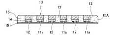
本願の一実施形態の発光装置の製造方法は、図1A〜1Fに示すように、
透光板11の上面と、この上面と反対側の下面とに遮光膜12を形成し(図1A)、
遮光膜12とともに透光板11を上面から下面又は下面から上面に向かって切断して複数の板状の光学部品13を形成し(図1B)、
側面視において、光学部品13の切断面11aと遮光膜12とが列方向に交互に並ぶように、光学部品13の切断面11aを発光素子14の上に固定し(図1C)、発光素子14を基板15上に列状又は行列状に配列する(図1D)ことを含む。
このような構成を備えることにより、発光装置全体の輝度の低下を最小限に留めると同時に、隣接する発光面の点灯/消灯間との輝度差が急峻で、かつ所望の配光性を有する発光装置を容易かつ簡便に製造することが可能となる。
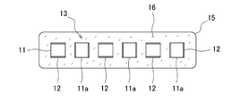
このような発光装置の製造方法では、さらに、図2に示すように、側面視(矢印B)において光学部品13の切断面11aと遮光膜12とが行方向に交互に並ぶように、発光素子14を基板15上に行状に配列してもよいし、図1E等に示すように、基板15上であって、発光素子14の側面を光反射性部材16で被覆してもよいし、光学部品13の側面を光反射性部材16で被覆してもよい。[Manufacturing method of light emitting device]
The method for manufacturing the light emitting device according to the embodiment of the present application is as shown in FIGS. 1A to 1F.
A light-
A plurality of plate-shaped
In the side view, the
By providing such a configuration, the decrease in the brightness of the entire light emitting device is minimized, and at the same time, the brightness difference between the lighting and extinguishing of the adjacent light emitting surfaces is steep, and the light emission has a desired light distribution property. The device can be manufactured easily and easily.
In the method of manufacturing such a light emitting device, as shown in FIG. 2, the light emitting element is further arranged so that the
(遮光膜12の形成)
図1Aに示すように、まず、透光板11を準備する。
透光板は、発光素子からの光(例えば、波長320nm〜850nmの範囲の光)の60%以上を透過するものが挙げられ、70%以上の光を透過するものが好ましい。また、板状の部材であるものが好ましく、上面及び上面と反対側の下面を有する板状部材であるものが好ましい。上面及び下面は、平行であることが好ましいが、それらの表面に凹凸が存在していてもよい。本明細書においては、「平行」は、一面に対する他面の傾斜が±10°程度変動することが許容される。
透光板の大きさ、形状及び厚みは、製造しようとする発光装置の大きさ、数等によって適宜設定することができる。例えば、透光板の厚みは、10μm〜1000μmが挙げられ、30μm〜500μmが好ましい。(Formation of light-shielding film 12)
As shown in FIG. 1A, first, the
Examples of the light transmitting plate include those that transmit 60% or more of the light from the light emitting element (for example, light in the wavelength range of 320 nm to 850 nm), and those that transmit 70% or more of the light are preferable. Further, a plate-shaped member is preferable, and a plate-shaped member having an upper surface and a lower surface opposite to the upper surface is preferable. The upper surface and the lower surface are preferably parallel, but irregularities may be present on their surfaces. In the present specification, "parallel" allows the inclination of the other surface with respect to one surface to fluctuate by about ± 10 °.
The size, shape, and thickness of the light-transmitting plate can be appropriately set depending on the size, number, and the like of the light emitting device to be manufactured. For example, the thickness of the light transmitting plate is 10 μm to 1000 μm, preferably 30 μm to 500 μm.
透光板11は、例えば、ガラス、セラミックス、サファイア等の無機材料、シリコーン樹脂、変性シリコーン樹脂、エポキシ樹脂、変性エポキシ樹脂、アクリル樹脂、フェノール樹脂、フッ素樹脂の1種以上を含む樹脂又はハイブリッド樹脂等の有機材料のいずれによって形成されていてもよい。
透光板11には、蛍光体、光拡散材等が含有されていてもよいし、透光板11の上面及び/又は下面に、蛍光体層、光拡散材層等が形成されていてもよい。
蛍光体としては、用いようとする発光素子からの光で励起可能なものであればよい。例えば、セリウムで賦活されたイットリウム・アルミニウム・ガーネット系蛍光体(例えば、Y3(Al,Ga)5O12:Ce)、セリウムで賦活されたルテチウム・アルミニウム・ガーネット系蛍光体(例えば、Lu3(Al,Ga)5O12:Ce)、ユウロピウムおよび/又はクロムで賦活された窒素含有アルミノ珪酸カルシウム系蛍光体(例えば、CaO−Al2O3−SiO2:Eu)、ユウロピウムで賦活されたシリケート系蛍光体(例えば(Sr,Ba)2SiO4:Eu)、βサイアロン系蛍光体(例えば、Si6-zAlzOzN8-z:Eu(0<Z<4.2))、CASN系蛍光体(例えば、CaAlSiN3:Eu)、SCASN系蛍光体(例えば、(Sr,Ca)AlSiN3:Eu)等の窒化物系蛍光体、マンガンで賦活されたフッ化珪酸カリウム系蛍光体(例えば、K2SiF6:Mn)、硫化物系蛍光体、量子ドット蛍光体などが挙げられる。これらは1種のみ又は2種以上を組み合わせて用いることができる。例えば、これらの蛍光体と、青色発光素子又は紫外線発光素子と組み合わせることにより、所望の発光色の発光装置(例えば白色系の発光装置)を得ることができる。白色に発光可能な発光装置とする場合、蛍光体層に含有される蛍光体の種類、濃度によって白色となるよう調整される。このような蛍光体が透光性材料に含有される場合、蛍光体の濃度を、例えば30%〜80%程度とすることが好ましい。
光拡散材としては、シリカ、酸化チタン、酸化ジルコニウム、酸化マグネシウム、アエロジル、ガラス、ガラスファイバー又はワラストナイトなどのフィラー、窒化アルミニウム等が挙げられる。
なお、蛍光体を含む透光板は、例えば、蛍光体の焼結体、樹脂、ガラス、無機物等の透光性材料を蛍光体のバインダーとして混合して成形したものであってもよい。
蛍光体層を透光板の上面及び/又は下面に配置する場合、その厚みは、蛍光体層を構成する材料、蛍光体の含有量等によって適宜設定することができる。なかでも、蛍光体層は薄層であることが好ましく、例えば、50μm以下であることが好ましく、40μm以下がより好ましい。
蛍光体層は、上述した材料を用いて、板状に成型し、所望の形状に分割して形成することができる。また、透光板11の一面に印刷、塗工、噴霧等により蛍光体層を形成してもよい。
透光板に蛍光体が含有されているか、蛍光体層がその上又は下面に配置されていることにより、蛍光体と透光板とを一括して発光素子上に載置することができるため、製造工程を簡略化することができる。The
The
The phosphor may be any phosphor that can be excited by light from the light emitting element to be used. For example, a cerium-activated yttrium-aluminum-garnet phosphor (eg, Y3 (Al, Ga)5 O12 : Ce), a cerium-activated lutetium-aluminum-garnet phosphor (eg, Lu3). (Al, Ga)5 O12 : Ce), europium and / or chromium-activated nitrogen-containing calcium aluminosilicate phosphor (eg, CaO-Al2 O3- SiO2 : Eu), activated with europium. Silicate phosphors (eg (Sr, Ba)2 SiO4 : Eu), β-sialon phosphors (eg Si6-z Alz Oz N8-z : Eu (0 <Z <4.2)) , CASN-based phosphors (eg, CaAlSiN3 : Eu), SCASN-based phosphors (eg, (Sr, Ca) AlSiN3 : Eu) and other nitride-based phosphors, manganese-activated potassium fluoride silicate-based phosphors Examples thereof include a body (for example, K2 SiF6 : Mn), a sulfide-based phosphor, and a quantum dot phosphor. These can be used alone or in combination of two or more. For example, by combining these phosphors with a blue light emitting element or an ultraviolet light emitting element, a light emitting device having a desired light emitting color (for example, a white light emitting device) can be obtained. When the light emitting device is capable of emitting white light, it is adjusted to be white depending on the type and concentration of the phosphor contained in the phosphor layer. When such a fluorescent substance is contained in the translucent material, the concentration of the fluorescent substance is preferably set to, for example, about 30% to 80%.
Examples of the light diffusing material include silica, titanium oxide, zirconium oxide, magnesium oxide, aerosil, glass, a filler such as glass fiber or wallastnite, and aluminum nitride.
The translucent plate containing the phosphor may be formed by mixing, for example, a translucent material such as a sintered body of the phosphor, a resin, glass, or an inorganic substance as a binder of the phosphor.
When the phosphor layer is arranged on the upper surface and / or the lower surface of the light transmitting plate, the thickness thereof can be appropriately set depending on the material constituting the phosphor layer, the content of the phosphor, and the like. Among them, the phosphor layer is preferably a thin layer, for example, preferably 50 μm or less, and more preferably 40 μm or less.
The phosphor layer can be formed by molding it into a plate shape using the above-mentioned material and dividing it into a desired shape. Further, a phosphor layer may be formed on one surface of the
Since the light-transmitting plate contains a phosphor or the phosphor layer is arranged on the upper surface or the lower surface thereof, the phosphor and the light-transmitting plate can be collectively placed on the light emitting element. , The manufacturing process can be simplified.
続いて、準備した透光板11の上面及び下面に遮光膜12を形成する。
遮光膜12は、発光素子からの光を80%以上遮光し得る材料によって形成することが好ましい。
遮光膜12は、例えば、Ti、Cr、Ni、Si、Al、Ag、Au、Pt、Pd等の金属又はその合金、誘電体等によって形成することができる。誘電体は、例えば、任意に酸化膜等からなる下地層の上に、低屈折率層と高屈折率層とを積層させた多層構造とするものが挙げられ、所定の波長光を選択的に反射するようにDBR(分布ブラッグ反射器)膜として構成されているものが挙げられる。具体的には屈折率の異なる膜を、発光素子の波長、蛍光体の波長又はこれらの波長の中間の波長の1/4程度の厚みで交互に積層することにより、所定の波長を高効率に反射させることができる。材料として、Si、Ti、Zr、Nb、Ta、Alからなる群より選択された少なくとも一種の酸化物又は窒化物を含んで形成することができる。
遮光膜は、例えば、スパッタ法、真空蒸着法、原子層堆積法等、当該分野で公知の方法によって形成することができる。
遮光膜の膜厚は、例えば、0.2μm〜5μmが挙げられ、0.5μm〜2μmが好ましい。Subsequently, the light-shielding
The light-shielding
The light-shielding
The light-shielding film can be formed by a method known in the art, such as a sputtering method, a vacuum vapor deposition method, or an atomic layer deposition method.
The film thickness of the light-shielding film is, for example, 0.2 μm to 5 μm, preferably 0.5 μm to 2 μm.
(光学部品13の形成)
図1Bに示すように、上述した遮光膜12が形成された透光板11を、遮光膜12とともに上面から下面又は下面から上面に向かって切断することによって、複数の板状の光学部品13を形成することができる。
ここでの切断は、遮光膜12が形成された透光板11の上面及び/又は下面に対して切断面が垂直になるように行うことが好ましい。本明細書において「垂直」は、±10%以内の傾きが許容される。また、この切断は、平面視において一方向、例えば、透光板の一辺に平行に、複数回行うことが好ましい。さらに、一方向に交差する方向、例えば、直交する方向に、複数回行うことがより好ましい。このような切断によって、上下面に遮光膜を有する透光板の小片(以下「透光片」ということがある)が得られる。また、容易に、平面形状が四角形である透光片を複数得ることができる。
切断された複数の光学部品の大きさ及び形成等は、得ようとする発光装置の形態によって適宜設定することができる。例えば、平面視、一辺が400μm〜1500μmの四角形が挙げられる。
光学部品においては、その上面積及び下面積が同じであってもよいが、上面積が下面積よりも大きくても、小さくてもよい。つまり、この工程での透光板11の切断は、遮光膜が形成された面、つまり透光板の上下面に対して傾斜して行ってもよい。このような切断は、特定の方向への配光を意図する光学部品を製造する場合に利用することができる。ここでの上面積と下面積との面積差は、例えば、上又は下面積の1%〜20%が挙げられる。(Formation of optical component 13)
As shown in FIG. 1B, a plurality of plate-shaped
The cutting here is preferably performed so that the cut surface is perpendicular to the upper surface and / or the lower surface of the
The size and formation of the plurality of cut optical components can be appropriately set depending on the form of the light emitting device to be obtained. For example, in a plan view, a quadrangle having a side of 400 μm to 1500 μm can be mentioned.
In the optical component, the upper area and the lower area may be the same, but the upper area may be larger or smaller than the lower area. That is, the cutting of the light-transmitting
なお、光学部品13は、後述するように、発光素子の光取り出し面、つまり上面の上に固定されるが、その際、光学部品の下面積が、発光素子の光取り出し面の平面積と同等又はそれよりも大きいことが好ましい。これにより、発光素子と光学部品との接合のために接合部材を用いる場合、光学部品の側面への接合部材の漏れ及び這い上がりを防止することができる。また、発光面間の距離を小さくすることができる。下面積の大きさは、例えば、発光素子14の光取り出し面の100%〜130%が挙げられ、103%〜120%が好ましく、104%〜110%がより好ましい。また、光学部品の外縁の全てが、平面視、発光素子の外縁と一致するか、または外縁よりも外側に配置されるような大きさ及び形状であることが好ましく、光学部品の外縁の全てが、平面視、発光素子の外縁よりも外側に配置されるような大きさ及び形状であることがより好ましい。このような配置により、発光素子の光取り出し面から出射される光を光学部品に効率的に入射させることができる。さらに、隣接する光学部品13間の距離を発光素子間の距離と同等以下とすることができるので、発光装置の発光面間を狭くすることができ好ましい。 As will be described later, the
(光学部品13の発光素子14上への固定及び発光素子14の基板15への配列)
まず、発光素子14を複数準備する。
次に、例えば、図1Cに示すように、複数の発光素子14のそれぞれの上に光学部品13を固定する。
光学部品13の発光素子14上への固定は、発光素子14の上面と、光学部品13の切断面11aとが対向するように固定する。言い換えると、光学部品13の遮光膜12が、発光素子14の側面と平行となるように固定する。
光学部品の発光素子への固定と、発光素子の基板への配列は、いずれを先に行ってもよい。つまり、光学部品の発光素子への固定を行った後、発光素子の基板への配列を行うか、又は発光素子の基板への配列を行った後、光学部品の発光素子への固定を行う。ただし、いずれの場合においても、これらの工程の後において得られた発光装置は、側面視において、発光素子14上に固定された光学部品13の切断面11aと遮光膜12とが列方向に交互に並ぶように、発光素子14及び光学部品13とを配列した状態とする。
例えば、図1Dに示すように、発光素子14を一列のみ配置する場合、側面視において、光学部品13の切断面11aと遮光膜12とを列方向に交互に配列する。言い換えると、図1Fに示すように、上面視において、光学部品13の一切断面11a又は一遮光膜12が、列方向に90°回転しながら基板15上に並ぶように、発光素子14を配列する。
また、発光素子14が行列状に配置する場合、図2の矢印A方向からの側面視において、光学部品13の切断面11aと遮光膜12とが列方向に交互に並ぶように、光学部品13を固定した発光素子14を配列する。同時に、図2の矢印B方向からの側面視においても、光学部品13の切断面11aと遮光膜12とが列方向に交互に並ぶように、光学部品13を固定した発光素子14を配列する。言い換えると、図2に示すように、上面視において、行列方向のいずれにおいても、光学部品13の一切断面11a又は一遮光膜12が、列方向に90°回転しながら基板15上に並ぶように、光学部品13を固定した発光素子14を配列する。(Fixing of the
First, a plurality of
Next, for example, as shown in FIG. 1C, the
The
Either fixing the optical component to the light emitting element or arranging the light emitting element on the substrate may be performed first. That is, after fixing the optical component to the light emitting element, the light emitting element is arranged on the substrate, or after the light emitting element is arranged on the substrate, the optical component is fixed to the light emitting element. However, in any case, in the light emitting device obtained after these steps, the
For example, as shown in FIG. 1D, when the
When the
一般に、複数配列した発光素子において、隣接する発光素子が点灯/消灯状態の際にそれぞれの発光素子の輝度差を急峻とするためには、例えば、四角形の光学部品21の場合には、図3Aに示すように、その4側面に遮光膜22を配置することが有効である。その一方、遮光膜22は、少なからず光を吸収する。そのため、4側面に遮光膜22を有する光学部品21を発光素子の上に固定し、上面から見た場合、発光素子の発光面の遮光膜22の近傍領域28では、その明るさ及び輝度が低下する。従って、図3A及び3Bに示すように、遮光膜22を、光学部品の4側面又は隣接する2側面に配置すると、上面から見た場合、遮光膜22で挟まれた角領域、つまり遮光膜22の近傍領域28が重なる領域29では著しく明るさ及び輝度が低くなる。
これに対して、上述し、かつ図3Cに示すように、遮光膜22が、光学部品21の対向する2側面にのみ配置し、その他の2側面を切断面21aとする場合、それを上面から見ると、発光素子の発光面の遮光膜22の近傍領域28が対向する2側面にのみ配置されるため、その重なる領域29のような、著しく明るさ及び輝度が低い領域の発生を防止することができる。その結果、複数の発光素子が配列された発光装置の全面において、その明るさ及び輝度の低下を極力低減して、本来の明るさ及び輝度を維持することが可能となる。同時に、発光素子の列方向又は行列方向における、隣り合う二方向又は四方向において、遮光することができる。そのため、隣接する発光素子間での光漏れを抑制することが可能となる。これにより、例えば、非発光部と発光部との間の輝度差を急峻にすることができ、所望の配光を得ることができる。このような発光装置は、例えば、自動車用ヘッドライト、特に、配光可変型のヘッドライトに有利に利用することができる。Generally, in a plurality of arranged light emitting elements, in order to make the brightness difference between the adjacent light emitting elements steep when the adjacent light emitting elements are lit / extinguished, for example, in the case of a square
On the other hand, as described above and as shown in FIG. 3C, when the light-shielding
光学部品は、接合部材を介して又は介さずに発光素子の上に固定することができる。接合部材としては、透光性の接合部材もしくは高屈折率の有機接着剤を用いたものが利用できる。また、表面活性化接合型もしくは原子拡散接合型の常温接合を利用して、また圧着、焼結を利用して、発光素子の上に直接固定してもよい。
透光性の接合部材としては、発光素子からの光を60%又は70%以上透過する部材であって、例えば、透光板で例示した樹脂等を用いて形成することができる。接合部材には光拡散材、蛍光体等が含有されていてもよい。接合に用いられる材料は、発光素子の上面と光学部品との間で0μmに近い厚みで配置されることが好ましく、例えば10μm以下、具体的には3μm〜7μm程度で配置されることがより好ましい。また、接合部材は、発光素子の側面の一部又は全部を被覆するように配置されていてもよい。この場合、発光素子の側面から光学部品の下面に亘ってフィレット状に広がるように配置されることが好ましい。The optics can be fixed onto the light emitting element with or without a joining member. As the joining member, a translucent joining member or a member using an organic adhesive having a high refractive index can be used. Further, it may be directly fixed on the light emitting element by using a surface activation bonding type or an atomic diffusion bonding type normal temperature bonding, or by using pressure bonding and sintering.
The translucent bonding member is a member that transmits 60% or 70% or more of the light from the light emitting element, and can be formed by using, for example, the resin exemplified in the translucent plate. The joining member may contain a light diffusing material, a phosphor, or the like. The material used for bonding is preferably arranged with a thickness close to 0 μm between the upper surface of the light emitting element and the optical component, and more preferably 10 μm or less, specifically about 3 μm to 7 μm. .. Further, the joining member may be arranged so as to cover a part or all of the side surface of the light emitting element. In this case, it is preferable that the light emitting element is arranged so as to spread in a fillet shape from the side surface to the lower surface of the optical component.
複数の発光素子14は、互いに離間して、基板15上へ配列することが好ましい。また、基板15上に搭載された発光素子14上の光学部品13も、互いに離間していることが好ましい。例えば、発光素子14又は光学部品13間の距離は、30μm〜100μmが挙げられ、50μm〜70μmが好ましい。このような間隔に設定することにより、複数の発光素子を部分的に点灯させた際に、発光装置の発光面側において、点灯している発光素子から、これに隣接する消灯している発光素子上に位置する光学部品への光漏れを抑制することが可能となる。これにより、発光部と、非発光部との輝度差が急峻な発光装置を得ることができる。 It is preferable that the plurality of
基板は、発光素子が実装されるために用いられるいずれの基板を用いてもよい。例えば、ガラスエポキシ、樹脂、セラミックスなどの絶縁性部材、表面に絶縁部材を形成した金属部材等が挙げられる。なかでも、耐熱性及び耐候性の高いセラミックスを利用したものが好ましい。セラミックス材料としては、アルミナ、窒化アルミニウム、ムライトなどが挙げられ、これらのセラミックス材料に、例えば、BTレジン、ガラスエポキシ、エポキシ系樹脂等の絶縁性材料を組み合わせてもよい。基板は、通常、その表面に発光素子と接続される配線を有するものが好ましい。配線は、発光素子が、基板上において、任意に駆動し得るように形成されていることが好ましく、なかでも、複数の発光素子を個別に駆動し得るように形成されていることがより好ましい。 As the substrate, any substrate used for mounting the light emitting element may be used. Examples thereof include insulating members such as glass epoxy, resin, and ceramics, and metal members having an insulating member formed on the surface. Among them, those using ceramics having high heat resistance and weather resistance are preferable. Examples of the ceramic material include alumina, aluminum nitride, mullite, and the like, and an insulating material such as BT resin, glass epoxy, or epoxy resin may be combined with these ceramic materials. The substrate is usually preferably one having wiring connected to the light emitting element on its surface. The wiring is preferably formed so that the light emitting element can be arbitrarily driven on the substrate, and more preferably, the light emitting element is formed so as to be able to individually drive a plurality of light emitting elements.
発光素子は、通常、発光ダイオードが用いられる。発光素子は、1つの発光装置において複数含まれている。
発光素子は、その組成、発光色又は波長、大きさ、個数等、目的に応じて適宜選択することができる。例えば、青色、緑色の発光素子としては、ZnSe、窒化物系半導体(InXAlYGa1-X-YN、0≦X、0≦Y、X+Y≦1)、GaPなどの半導体層を用いたもの、赤色の発光素子としては、GaAlAs、AlInGaPなどの半導体層を用いたものが挙げられる。
発光素子は、通常、透光性の支持基板(例えば、サファイア基板)上に、半導体層を積層させて形成される。基板が発光素子の上面側となり、発光素子の主な光取り出し面となる。支持基板は半導体層との接合面に凹凸を有していてもよい。これにより半導体層から出射された光が、基板に当たるときの臨界角を意図的に変えて、基板の外部に光を容易に取り出すことができる。
発光素子においては、支持基板は半導体層の積層後に除去されていてもよい。除去は、例えば、研磨、LLO(レーザ・リフト・オフ)等で行うことができる。支持基板が除去された場合は、支持基板に最も近かった半導体層の表面が発光素子の上面となり、発光素子の主な光取り出し面となる。
発光素子は、同一面側に正負一対の電極を有するものが好ましい。これにより、発光素子を実装基板にフリップチップ実装することができる。そして、一対の電極が形成された面と対向する面が光取り出し面となる。
発光素子の数は、得ようとする発光装置の特性、サイズ等に応じて適宜設定することができる。複数の発光素子は、互いに近接して整列していることが好ましい。発光装置の輝度分布、さらに車両用途として用いること等を考慮すると、隣接する発光素子間の距離は個々の発光素子のサイズ(例えば一辺の長さ)よりも短いものが好ましく、例えば、発光素子自体のサイズの30%程度以下がより好ましく、20%以下がさらに好ましい。具体的には、発光素子の大きさにもよるが、例えば、30μm〜300μmが挙げられ、40μm〜100μmが好ましく、50μm〜80μmがより好ましい。A light emitting diode is usually used as the light emitting element. A plurality of light emitting elements are included in one light emitting device.
The light emitting element can be appropriately selected depending on the purpose, such as its composition, light emitting color or wavelength, size, number, and the like. For example, as the blue and green light emitting elements,a semiconductor layer such as ZnSe, a nitride semiconductor (In X AlY Ga1-XY N, 0 ≦ X, 0 ≦ Y, X + Y ≦ 1), or GaP is used. Examples of the red light emitting element include those using a semiconductor layer such as GaAlAs and AlInGaP.
The light emitting element is usually formed by laminating a semiconductor layer on a translucent support substrate (for example, a sapphire substrate). The substrate is on the upper surface side of the light emitting element and serves as the main light extraction surface of the light emitting element. The support substrate may have irregularities on the joint surface with the semiconductor layer. As a result, the critical angle when the light emitted from the semiconductor layer hits the substrate can be intentionally changed, and the light can be easily taken out to the outside of the substrate.
In the light emitting device, the support substrate may be removed after the semiconductor layers are laminated. The removal can be performed by, for example, polishing, LLO (laser lift off), or the like. When the support substrate is removed, the surface of the semiconductor layer closest to the support substrate becomes the upper surface of the light emitting element and becomes the main light extraction surface of the light emitting element.
The light emitting element preferably has a pair of positive and negative electrodes on the same surface side. As a result, the light emitting element can be flip-chip mounted on the mounting substrate. The surface facing the surface on which the pair of electrodes is formed becomes the light extraction surface.
The number of light emitting elements can be appropriately set according to the characteristics, size, and the like of the light emitting device to be obtained. It is preferable that the plurality of light emitting elements are aligned close to each other. Considering the brightness distribution of the light emitting device and the use for vehicles, the distance between adjacent light emitting elements is preferably shorter than the size of each light emitting element (for example, the length of one side), for example, the light emitting element itself. It is more preferably about 30% or less of the size of the above, and further preferably 20% or less. Specifically, although it depends on the size of the light emitting element, for example, 30 μm to 300 μm is mentioned, 40 μm to 100 μm is preferable, and 50 μm to 80 μm is more preferable.
(光反射性部材16の形成)
発光装置の製造方法では、図1Eに示すように、基板15上に搭載された発光素子14の側面の一部又は全部を被覆する光反射性部材16を形成することが好ましい。光反射性部材16は、発光素子14の側面に加えて、光学部品13の側面の一部又は全部を被覆してもよい。なかでも、光反射性部材16は、発光素子14の側面の全部及び光学部品13の側面の全部を被覆することが好ましい。また、光反射性部材16の上面は、光学部品13の上面に対して突出していてもよいが、凹んでいるか、光反射性部材16の上面と光学部品13の上面とが面一であることがより好ましい。
一般に、光出射面となる光学部品の上面から出射された光は、横方向にも広がりを有する。光反射性部材の上面が、光学部品の上面の高さよりも高い場合には、光学部品の上面から出射された光が光反射性部材に当たって反射され、配光のばらつきが生じる。これに対して、光学部品の側面を光反射性部材で覆いつつ、その側面の外周を覆う光反射性部材の高さをそれと同じか、低くすることにより、出射された光の全部を外部に直接取り出すことができる。(Formation of Light Reflective Member 16)
In the method of manufacturing the light emitting device, as shown in FIG. 1E, it is preferable to form the
In general, the light emitted from the upper surface of the optical component serving as the light emitting surface has a spread in the lateral direction. When the upper surface of the light-reflecting member is higher than the height of the upper surface of the optical component, the light emitted from the upper surface of the optical component hits the light-reflecting member and is reflected, resulting in variation in light distribution. On the other hand, while covering the side surface of the optical component with a light-reflecting member, the height of the light-reflecting member covering the outer periphery of the side surface is made the same as or lower than that, so that all the emitted light is exposed to the outside. Can be taken out directly.
光反射性部材は、発光素子から出射される光を反射することができる材料から形成される。これによって、光学部品13又は発光素子14と光反射性部材16との界面で、発光素子から出射される光を、光学部品13又は発光素子14内に反射させ、それにより、効率的に、光学部品13の上面から、外部へと出射させることができる。
光反射性部材は、絶縁材料を用いることが好ましく、例えば、樹脂材料を用いて形成することができる。樹脂材料としては、シリコーン樹脂、変性シリコーン樹脂、エポキシ樹脂、変性エポキシ樹脂、アクリル樹脂、フェノール樹脂、フッ素樹脂の1種以上を含む樹脂又はハイブリッド樹脂が挙げられる。光反射性部材は、これらの樹脂材料に、光反射性物質を含有させることにより形成することができる。光反射性物質としては、酸化チタン、酸化ケイ素、酸化ジルコニウム、チタン酸カリウム、アルミナ、窒化アルミニウム、窒化ホウ素、ムライトなどが挙げられる。
光反射性部材は、隣接する透光性部材間の距離によって光の反射量、透過量等を変動させることができるため、反射性物質の含有量は、得ようとする発光装置の特性等によって適宜調整することができる。例えば、光反射性部材の全重量に対して反射性物質の含有量を30wt%以上とし、その厚みを50μm以上又は100μm以上とすることが好ましい。
光反射性部材は、例えば、射出成形、ポッティング成形、樹脂印刷法、トランスファーモールド法、圧縮成形などにより成形することができる。The light-reflecting member is formed of a material capable of reflecting the light emitted from the light emitting element. As a result, the light emitted from the light emitting element is reflected in the
The light-reflecting member preferably uses an insulating material, and can be formed, for example, by using a resin material. Examples of the resin material include a silicone resin, a modified silicone resin, an epoxy resin, a modified epoxy resin, an acrylic resin, a phenol resin, and a resin containing at least one of a fluororesin or a hybrid resin. The light-reflecting member can be formed by incorporating a light-reflecting substance in these resin materials. Examples of the light-reflecting substance include titanium oxide, silicon oxide, zirconium oxide, potassium titanate, alumina, aluminum nitride, boron nitride, and mullite.
Since the light-reflecting member can vary the amount of light reflected, the amount of light transmitted, etc. depending on the distance between adjacent translucent members, the content of the reflective substance depends on the characteristics of the light emitting device to be obtained, etc. It can be adjusted as appropriate. For example, it is preferable that the content of the reflective substance is 30 wt% or more and the thickness thereof is 50 μm or more or 100 μm or more with respect to the total weight of the light-reflecting member.
The light-reflecting member can be molded by, for example, injection molding, potting molding, resin printing method, transfer molding method, compression molding, or the like.
〔発光装置〕
本願の一実施形態の発光装置は、図1E及び1Fに示すように、遮光膜12が配置された対向する二側面と、遮光膜12が配置されていない対向する二側面とを有する板状の光学部品13及び基板15上に列状又は行列状に配列された複数の発光素子14を備え、光学部品13の遮光膜12が配置された側面と遮光膜12が配置されていない側面とが、側面視において列に沿って交互に並ぶように、光学部品13が発光素子14の上に配置されている。また、基板15上であって発光素子14及び光学部品13の側面を被覆する光反射性部材16を備えている。ここで、遮光膜12が配置されていない側面とは、上述したように、切断面11aを意味する。
例えば、発光装置をヘッドランプ等に組み込んだ際には、不要な光が不要な箇所を照らすことを阻止すること、また、グレア光を回避すること、発光部と非発光部との境界がはっきりしている(見切り性が良い)ことが重要である。
この実施形態の発光装置においては、発光面間の距離を最小限に設定しながら、発光素子から出射され、光学部品に入射した光の横方向及び/又は縦方向への伝播を抑制し、横方向及び/又は縦方向への漏れ光を確実に防止することができる。その結果、発光装置のさらなる小型化を図りながら、発光素子の点灯/消灯間又は発光部(発光素子の光取り出し面)と、非発光部(発光素子間)との輝度差が急峻な高いコントラストを得ることができる。
つまり、図3Cに示すように、上面から見た場合、発光素子の発光面の遮光膜22の近傍領域28が対向する2側面にのみ配置されるため、図3A及び図3Bに示す遮光膜22の近傍領域が重なる領域29のような、著しく明るさ及び輝度が低い領域の発生を防止することができる。その結果、複数の発光素子が配列された発光装置の全面において、その明るさ及び輝度の低下を極力低減して、本来の明るさ及び輝度を維持することが可能となる。同時に、発光素子の列方向又は行列方向における、隣り合う二方向又は四方向において、遮光することができる。特に、行列方向に、上述した発光素子及び光学部品が配列される場合には、その明るさ及び輝度が低下する遮光膜22の近傍領域28の重なる領域29を生じさせることなく、隣接する発光素子の上に配置された光学部品の遮光膜22により、四方向において、点灯する発光素子の光を遮光することができる。そのため、隣接する発光素子間での光漏れを抑制することが可能とり、非発光部と発光部との間の輝度差を急峻にすることができ、所望の配光を得ることができる。
なお、このような発光装置には、例えば、図2に示したように、保護素子等の電子部品17が搭載されてもよい。電子部品17は、例えば、光反射性部材16内に埋設することができる。これにより、発光素子14からの光が電子部品に吸収されたり、電子部品に遮光されたりすることによる光取り出しの低下を防止することができる。[Light emitting device]
As shown in FIGS. 1E and 1F, the light emitting device according to the embodiment of the present application has a plate-like shape having two opposing side surfaces in which the light-shielding
For example, when a light emitting device is incorporated into a headlamp or the like, it is possible to prevent unnecessary light from illuminating an unnecessary part, avoid glare light, and clearly define a boundary between a light emitting part and a non-light emitting part. It is important that the light is closed (good closeout).
In the light emitting device of this embodiment, while setting the distance between the light emitting surfaces to the minimum, the light emitted from the light emitting element and incident on the optical component is suppressed from propagating in the horizontal direction and / or the vertical direction, and laterally. Leakage of light in the directional and / or vertical direction can be reliably prevented. As a result, while further reducing the size of the light emitting device, the brightness difference between the lighting / extinguishing of the light emitting element or the light emitting portion (light extraction surface of the light emitting element) and the non-light emitting portion (between the light emitting elements) is steep and high contrast. Can be obtained.
That is, as shown in FIG. 3C, when viewed from the upper surface, the
As shown in FIG. 2, for example, an
本開示の発光装置は、自動車用ヘッドライト、特に、配光可変型のヘッドライトに有利に利用することができる。さらに、照明用光源、各種インジケーター用光源、車載用光源、ディスプレイ用光源、液晶のバックライト用光源、信号機、車載部品、看板用チャンネルレターなど、種々の光源に使用することができる。 The light emitting device of the present disclosure can be advantageously used for automobile headlights, particularly headlights having a variable light distribution type. Further, it can be used for various light sources such as a light source for lighting, a light source for various indicators, an in-vehicle light source, a light source for a display, a light source for a liquid crystal backlight, a traffic light, an in-vehicle component, and a channel letter for a signboard.
11 透光板
11a 切断面
12 遮光膜
13 光学部品
14 発光素子
15 基板
16 光反射性部材
17 電子部品
21 光学部品
21a 切断面
22 遮光膜
28 近傍領域
29 重なる領域11
Claims (9)
Translated fromJapanese前記遮光膜とともに前記透光板を前記上面から下面又は下面から上面に向かって切断して複数の板状の光学部品を形成し、
前記光学部品の切断面を発光素子の上に固定し、側面視において前記光学部品の切断面と前記遮光膜とが列方向に交互に並ぶように前記発光素子を基板上に列状又は行列状に配列することを含む発光装置の製造方法。A light-shielding film is formed on the upper surface of the light-transmitting plate and the lower surface opposite to the upper surface.
A plurality of plate-shaped optical components are formed by cutting the light-transmitting plate together with the light-shielding film from the upper surface to the lower surface or from the lower surface to the upper surface.
The cut surface of the optical component is fixed on the light emitting element, and the light emitting element is arranged in a row or a matrix on a substrate so that the cut surface of the optical component and the light shielding film are alternately arranged in a row direction in a side view. A method of manufacturing a light emitting device, which comprises arranging in.
基板上に列状又は行列状に配列された複数の発光素子を備え、
前記光学部品の前記遮光膜が配置された側面と前記遮光膜が配置されていない側面とが、側面視において列に沿って交互に並ぶように、前記光学部品が前記発光素子の上に配置されている発光装置。It is provided with a plate-shaped optical component having two opposite sides on which a light-shielding film is arranged and two opposite sides on which a light-shielding film is not arranged, and a plurality of light emitting elements arranged in a row or a matrix on a substrate. ,
The optical component is arranged on the light emitting element so that the side surface on which the light-shielding film is arranged and the side surface on which the light-shielding film is not arranged are arranged alternately along a row in a side view. Light emitting device.
Priority Applications (3)
| Application Number | Priority Date | Filing Date | Title |
|---|---|---|---|
| JP2019080754AJP6947990B2 (en) | 2019-04-22 | 2019-04-22 | Manufacturing method of light emitting device and light emitting device |
| US16/842,661US11355682B2 (en) | 2019-04-22 | 2020-04-07 | Method of manufacturing light emitting device and light emitting device |
| CN202010316002.7ACN111834348B (en) | 2019-04-22 | 2020-04-21 | Method for manufacturing light-emitting device and light-emitting device |
Applications Claiming Priority (1)
| Application Number | Priority Date | Filing Date | Title |
|---|---|---|---|
| JP2019080754AJP6947990B2 (en) | 2019-04-22 | 2019-04-22 | Manufacturing method of light emitting device and light emitting device |
Publications (2)
| Publication Number | Publication Date |
|---|---|
| JP2020177853A JP2020177853A (en) | 2020-10-29 |
| JP6947990B2true JP6947990B2 (en) | 2021-10-13 |
Family
ID=72831271
Family Applications (1)
| Application Number | Title | Priority Date | Filing Date |
|---|---|---|---|
| JP2019080754AActiveJP6947990B2 (en) | 2019-04-22 | 2019-04-22 | Manufacturing method of light emitting device and light emitting device |
Country Status (3)
| Country | Link |
|---|---|
| US (1) | US11355682B2 (en) |
| JP (1) | JP6947990B2 (en) |
| CN (1) | CN111834348B (en) |
Families Citing this family (2)
| Publication number | Priority date | Publication date | Assignee | Title |
|---|---|---|---|---|
| TWI720785B (en)* | 2020-01-15 | 2021-03-01 | 東貝光電科技股份有限公司 | Micro led light emitting device and manufacturing method thereof |
| JP2023073749A (en) | 2021-11-16 | 2023-05-26 | 日亜化学工業株式会社 | WAVELENGTH CONVERSION MEMBER AND MANUFACTURING METHOD THEREOF, LIGHT EMITTING DEVICE |
Family Cites Families (19)
| Publication number | Priority date | Publication date | Assignee | Title |
|---|---|---|---|---|
| EP2216834B1 (en)* | 2007-11-29 | 2017-03-15 | Nichia Corporation | Light-emitting apparatus |
| JP2010085588A (en)* | 2008-09-30 | 2010-04-15 | Sony Corp | Manufacturing method of optical component, and optical component, and manufacturing method of display device, and display device |
| JP2011108588A (en)* | 2009-11-20 | 2011-06-02 | Koito Mfg Co Ltd | Light emitting module and vehicle lamp |
| JP2012169189A (en)* | 2011-02-15 | 2012-09-06 | Koito Mfg Co Ltd | Light-emitting module and vehicular lamp |
| JP5634647B1 (en) | 2012-12-03 | 2014-12-03 | シチズンホールディングス株式会社 | LED module |
| JP6153327B2 (en) | 2013-01-22 | 2017-06-28 | シチズン電子株式会社 | LED module |
| JP6186904B2 (en)* | 2013-06-05 | 2017-08-30 | 日亜化学工業株式会社 | Light emitting device |
| US9920889B2 (en) | 2013-10-11 | 2018-03-20 | Citizen Electronics Co., Ltd. | Lighting device including phosphor cover and method of manufacturing the same |
| JP6301099B2 (en) | 2013-10-11 | 2018-03-28 | シチズン電子株式会社 | Multicolor phosphor sheet, method for producing the same, and LED light emitting device using the multicolor phosphor sheet |
| JP6221668B2 (en)* | 2013-11-18 | 2017-11-01 | 日亜化学工業株式会社 | Manufacturing method of light distribution member and manufacturing method of light emitting device |
| JP5808840B2 (en) | 2014-05-26 | 2015-11-10 | 株式会社小糸製作所 | Light emitting module and vehicle lamp |
| JP6486078B2 (en) | 2014-11-21 | 2019-03-20 | スタンレー電気株式会社 | Light emitting device |
| US10415795B2 (en) | 2015-05-15 | 2019-09-17 | Nichia Corporation | Method of manufacturing light distribution member with shielded individual transmissive pieces and light-shielding frame, method of manufacturing light emitting device having light distribution member, light distribution member, and light emitting device |
| JP6265227B2 (en) | 2015-05-15 | 2018-01-24 | 日亜化学工業株式会社 | Light distribution member manufacturing method, light emitting device manufacturing method, light distribution member, and light emitting device |
| US10641437B2 (en) | 2016-06-30 | 2020-05-05 | Nichia Corporation | LED module |
| JP6380590B2 (en) | 2016-06-30 | 2018-08-29 | 日亜化学工業株式会社 | LED module |
| JP2018022844A (en)* | 2016-08-05 | 2018-02-08 | 日亜化学工業株式会社 | Light emitting apparatus and method of manufacturing the same |
| JP6645486B2 (en)* | 2017-02-13 | 2020-02-14 | 日亜化学工業株式会社 | Light emitting device and method of manufacturing the same |
| JP6485503B2 (en)* | 2017-08-01 | 2019-03-20 | 日亜化学工業株式会社 | Method for manufacturing light emitting device |
- 2019
- 2019-04-22JPJP2019080754Apatent/JP6947990B2/enactiveActive
- 2020
- 2020-04-07USUS16/842,661patent/US11355682B2/enactiveActive
- 2020-04-21CNCN202010316002.7Apatent/CN111834348B/enactiveActive
Also Published As
| Publication number | Publication date |
|---|---|
| JP2020177853A (en) | 2020-10-29 |
| CN111834348A (en) | 2020-10-27 |
| US11355682B2 (en) | 2022-06-07 |
| CN111834348B (en) | 2025-09-05 |
| US20200335676A1 (en) | 2020-10-22 |
Similar Documents
| Publication | Publication Date | Title |
|---|---|---|
| US10944030B2 (en) | Light emitting device | |
| US10141491B2 (en) | Method of manufacturing light emitting device | |
| JP6444299B2 (en) | Light emitting device | |
| JP6399017B2 (en) | Light emitting device | |
| US9722156B2 (en) | Light-emitting device | |
| JP6982233B2 (en) | Light emitting device and its manufacturing method | |
| JP6940776B2 (en) | Light emitting device and its manufacturing method | |
| KR20190038424A (en) | Light-emitting device | |
| WO2021002158A1 (en) | Method for manufacturing light emitting device and method for manufacturing light emitting module, and light emitting device and light emitting module | |
| JP6947990B2 (en) | Manufacturing method of light emitting device and light emitting device | |
| CN120201828A (en) | Light emitting device | |
| JP7177336B2 (en) | light emitting device | |
| US11050007B2 (en) | Light emitting device | |
| JP2024177546A (en) | Light-emitting device | |
| JP7575704B2 (en) | Light-emitting device | |
| JP7037078B2 (en) | Manufacturing method of light emitting device and manufacturing method of light emitting module, as well as light emitting device and light emitting module | |
| JP2021048218A (en) | Manufacturing method of light emitting module | |
| JP2025102623A (en) | Light-emitting device |
Legal Events
| Date | Code | Title | Description |
|---|---|---|---|
| A621 | Written request for application examination | Free format text:JAPANESE INTERMEDIATE CODE: A621 Effective date:20200622 | |
| A977 | Report on retrieval | Free format text:JAPANESE INTERMEDIATE CODE: A971007 Effective date:20210409 | |
| A131 | Notification of reasons for refusal | Free format text:JAPANESE INTERMEDIATE CODE: A131 Effective date:20210420 | |
| A521 | Request for written amendment filed | Free format text:JAPANESE INTERMEDIATE CODE: A523 Effective date:20210518 | |
| TRDD | Decision of grant or rejection written | ||
| A01 | Written decision to grant a patent or to grant a registration (utility model) | Free format text:JAPANESE INTERMEDIATE CODE: A01 Effective date:20210817 | |
| A61 | First payment of annual fees (during grant procedure) | Free format text:JAPANESE INTERMEDIATE CODE: A61 Effective date:20210830 | |
| R150 | Certificate of patent or registration of utility model | Ref document number:6947990 Country of ref document:JP Free format text:JAPANESE INTERMEDIATE CODE: R150 | |
| R250 | Receipt of annual fees | Free format text:JAPANESE INTERMEDIATE CODE: R250 | |
| R250 | Receipt of annual fees | Free format text:JAPANESE INTERMEDIATE CODE: R250 |