JP6932910B2 - Display device - Google Patents
Display deviceDownload PDFInfo
- Publication number
- JP6932910B2 JP6932910B2JP2016210490AJP2016210490AJP6932910B2JP 6932910 B2JP6932910 B2JP 6932910B2JP 2016210490 AJP2016210490 AJP 2016210490AJP 2016210490 AJP2016210490 AJP 2016210490AJP 6932910 B2JP6932910 B2JP 6932910B2
- Authority
- JP
- Japan
- Prior art keywords
- reflective layer
- display device
- semiconductor element
- sealing resin
- light
- Prior art date
- Legal status (The legal status is an assumption and is not a legal conclusion. Google has not performed a legal analysis and makes no representation as to the accuracy of the status listed.)
- Active
Links
Images


Classifications
- G—PHYSICS
- G02—OPTICS
- G02F—OPTICAL DEVICES OR ARRANGEMENTS FOR THE CONTROL OF LIGHT BY MODIFICATION OF THE OPTICAL PROPERTIES OF THE MEDIA OF THE ELEMENTS INVOLVED THEREIN; NON-LINEAR OPTICS; FREQUENCY-CHANGING OF LIGHT; OPTICAL LOGIC ELEMENTS; OPTICAL ANALOGUE/DIGITAL CONVERTERS
- G02F1/00—Devices or arrangements for the control of the intensity, colour, phase, polarisation or direction of light arriving from an independent light source, e.g. switching, gating or modulating; Non-linear optics
- G02F1/01—Devices or arrangements for the control of the intensity, colour, phase, polarisation or direction of light arriving from an independent light source, e.g. switching, gating or modulating; Non-linear optics for the control of the intensity, phase, polarisation or colour
- G02F1/13—Devices or arrangements for the control of the intensity, colour, phase, polarisation or direction of light arriving from an independent light source, e.g. switching, gating or modulating; Non-linear optics for the control of the intensity, phase, polarisation or colour based on liquid crystals, e.g. single liquid crystal display cells
- G02F1/133—Constructional arrangements; Operation of liquid crystal cells; Circuit arrangements
- G02F1/1333—Constructional arrangements; Manufacturing methods
- G02F1/1335—Structural association of cells with optical devices, e.g. polarisers or reflectors
- G02F1/1336—Illuminating devices
- G02F1/133602—Direct backlight
- G02F1/133603—Direct backlight with LEDs
- H—ELECTRICITY
- H10—SEMICONDUCTOR DEVICES; ELECTRIC SOLID-STATE DEVICES NOT OTHERWISE PROVIDED FOR
- H10H—INORGANIC LIGHT-EMITTING SEMICONDUCTOR DEVICES HAVING POTENTIAL BARRIERS
- H10H20/00—Individual inorganic light-emitting semiconductor devices having potential barriers, e.g. light-emitting diodes [LED]
- H10H20/80—Constructional details
- H10H20/85—Packages
- H10H20/855—Optical field-shaping means, e.g. lenses
- H10H20/856—Reflecting means
- G—PHYSICS
- G02—OPTICS
- G02B—OPTICAL ELEMENTS, SYSTEMS OR APPARATUS
- G02B6/00—Light guides; Structural details of arrangements comprising light guides and other optical elements, e.g. couplings
- G02B6/0001—Light guides; Structural details of arrangements comprising light guides and other optical elements, e.g. couplings specially adapted for lighting devices or systems
- G02B6/0011—Light guides; Structural details of arrangements comprising light guides and other optical elements, e.g. couplings specially adapted for lighting devices or systems the light guides being planar or of plate-like form
- G02B6/0033—Means for improving the coupling-out of light from the light guide
- G02B6/0035—Means for improving the coupling-out of light from the light guide provided on the surface of the light guide or in the bulk of it
- G02B6/0045—Means for improving the coupling-out of light from the light guide provided on the surface of the light guide or in the bulk of it by shaping at least a portion of the light guide
- G—PHYSICS
- G02—OPTICS
- G02F—OPTICAL DEVICES OR ARRANGEMENTS FOR THE CONTROL OF LIGHT BY MODIFICATION OF THE OPTICAL PROPERTIES OF THE MEDIA OF THE ELEMENTS INVOLVED THEREIN; NON-LINEAR OPTICS; FREQUENCY-CHANGING OF LIGHT; OPTICAL LOGIC ELEMENTS; OPTICAL ANALOGUE/DIGITAL CONVERTERS
- G02F1/00—Devices or arrangements for the control of the intensity, colour, phase, polarisation or direction of light arriving from an independent light source, e.g. switching, gating or modulating; Non-linear optics
- G02F1/01—Devices or arrangements for the control of the intensity, colour, phase, polarisation or direction of light arriving from an independent light source, e.g. switching, gating or modulating; Non-linear optics for the control of the intensity, phase, polarisation or colour
- G02F1/13—Devices or arrangements for the control of the intensity, colour, phase, polarisation or direction of light arriving from an independent light source, e.g. switching, gating or modulating; Non-linear optics for the control of the intensity, phase, polarisation or colour based on liquid crystals, e.g. single liquid crystal display cells
- G02F1/133—Constructional arrangements; Operation of liquid crystal cells; Circuit arrangements
- G02F1/1333—Constructional arrangements; Manufacturing methods
- G02F1/1335—Structural association of cells with optical devices, e.g. polarisers or reflectors
- G02F1/133553—Reflecting elements
- G—PHYSICS
- G02—OPTICS
- G02F—OPTICAL DEVICES OR ARRANGEMENTS FOR THE CONTROL OF LIGHT BY MODIFICATION OF THE OPTICAL PROPERTIES OF THE MEDIA OF THE ELEMENTS INVOLVED THEREIN; NON-LINEAR OPTICS; FREQUENCY-CHANGING OF LIGHT; OPTICAL LOGIC ELEMENTS; OPTICAL ANALOGUE/DIGITAL CONVERTERS
- G02F1/00—Devices or arrangements for the control of the intensity, colour, phase, polarisation or direction of light arriving from an independent light source, e.g. switching, gating or modulating; Non-linear optics
- G02F1/01—Devices or arrangements for the control of the intensity, colour, phase, polarisation or direction of light arriving from an independent light source, e.g. switching, gating or modulating; Non-linear optics for the control of the intensity, phase, polarisation or colour
- G02F1/13—Devices or arrangements for the control of the intensity, colour, phase, polarisation or direction of light arriving from an independent light source, e.g. switching, gating or modulating; Non-linear optics for the control of the intensity, phase, polarisation or colour based on liquid crystals, e.g. single liquid crystal display cells
- G02F1/133—Constructional arrangements; Operation of liquid crystal cells; Circuit arrangements
- G02F1/1333—Constructional arrangements; Manufacturing methods
- G02F1/1335—Structural association of cells with optical devices, e.g. polarisers or reflectors
- G02F1/1336—Illuminating devices
- G02F1/133602—Direct backlight
- G02F1/133605—Direct backlight including specially adapted reflectors
- H—ELECTRICITY
- H05—ELECTRIC TECHNIQUES NOT OTHERWISE PROVIDED FOR
- H05B—ELECTRIC HEATING; ELECTRIC LIGHT SOURCES NOT OTHERWISE PROVIDED FOR; CIRCUIT ARRANGEMENTS FOR ELECTRIC LIGHT SOURCES, IN GENERAL
- H05B33/00—Electroluminescent light sources
- H05B33/02—Details
- H05B33/04—Sealing arrangements, e.g. against humidity
- H—ELECTRICITY
- H05—ELECTRIC TECHNIQUES NOT OTHERWISE PROVIDED FOR
- H05B—ELECTRIC HEATING; ELECTRIC LIGHT SOURCES NOT OTHERWISE PROVIDED FOR; CIRCUIT ARRANGEMENTS FOR ELECTRIC LIGHT SOURCES, IN GENERAL
- H05B33/00—Electroluminescent light sources
- H05B33/10—Apparatus or processes specially adapted to the manufacture of electroluminescent light sources
- H—ELECTRICITY
- H10—SEMICONDUCTOR DEVICES; ELECTRIC SOLID-STATE DEVICES NOT OTHERWISE PROVIDED FOR
- H10H—INORGANIC LIGHT-EMITTING SEMICONDUCTOR DEVICES HAVING POTENTIAL BARRIERS
- H10H20/00—Individual inorganic light-emitting semiconductor devices having potential barriers, e.g. light-emitting diodes [LED]
- H10H20/80—Constructional details
- H10H20/84—Coatings, e.g. passivation layers or antireflective coatings
- H10H20/841—Reflective coatings, e.g. dielectric Bragg reflectors
- H—ELECTRICITY
- H10—SEMICONDUCTOR DEVICES; ELECTRIC SOLID-STATE DEVICES NOT OTHERWISE PROVIDED FOR
- H10H—INORGANIC LIGHT-EMITTING SEMICONDUCTOR DEVICES HAVING POTENTIAL BARRIERS
- H10H20/00—Individual inorganic light-emitting semiconductor devices having potential barriers, e.g. light-emitting diodes [LED]
- H10H20/80—Constructional details
- H10H20/85—Packages
- H10H20/851—Wavelength conversion means
- H—ELECTRICITY
- H10—SEMICONDUCTOR DEVICES; ELECTRIC SOLID-STATE DEVICES NOT OTHERWISE PROVIDED FOR
- H10H—INORGANIC LIGHT-EMITTING SEMICONDUCTOR DEVICES HAVING POTENTIAL BARRIERS
- H10H20/00—Individual inorganic light-emitting semiconductor devices having potential barriers, e.g. light-emitting diodes [LED]
- H10H20/80—Constructional details
- H10H20/85—Packages
- H10H20/852—Encapsulations
- H10H20/853—Encapsulations characterised by their shape
- H—ELECTRICITY
- H10—SEMICONDUCTOR DEVICES; ELECTRIC SOLID-STATE DEVICES NOT OTHERWISE PROVIDED FOR
- H10H—INORGANIC LIGHT-EMITTING SEMICONDUCTOR DEVICES HAVING POTENTIAL BARRIERS
- H10H20/00—Individual inorganic light-emitting semiconductor devices having potential barriers, e.g. light-emitting diodes [LED]
- H10H20/80—Constructional details
- H10H20/85—Packages
- H10H20/852—Encapsulations
- H10H20/854—Encapsulations characterised by their material, e.g. epoxy or silicone resins
- H—ELECTRICITY
- H01—ELECTRIC ELEMENTS
- H01L—SEMICONDUCTOR DEVICES NOT COVERED BY CLASS H10
- H01L25/00—Assemblies consisting of a plurality of semiconductor or other solid state devices
- H01L25/03—Assemblies consisting of a plurality of semiconductor or other solid state devices all the devices being of a type provided for in a single subclass of subclasses H10B, H10D, H10F, H10H, H10K or H10N, e.g. assemblies of rectifier diodes
- H01L25/04—Assemblies consisting of a plurality of semiconductor or other solid state devices all the devices being of a type provided for in a single subclass of subclasses H10B, H10D, H10F, H10H, H10K or H10N, e.g. assemblies of rectifier diodes the devices not having separate containers
- H01L25/075—Assemblies consisting of a plurality of semiconductor or other solid state devices all the devices being of a type provided for in a single subclass of subclasses H10B, H10D, H10F, H10H, H10K or H10N, e.g. assemblies of rectifier diodes the devices not having separate containers the devices being of a type provided for in group H10H20/00
- H01L25/0753—Assemblies consisting of a plurality of semiconductor or other solid state devices all the devices being of a type provided for in a single subclass of subclasses H10B, H10D, H10F, H10H, H10K or H10N, e.g. assemblies of rectifier diodes the devices not having separate containers the devices being of a type provided for in group H10H20/00 the devices being arranged next to each other
- H—ELECTRICITY
- H10—SEMICONDUCTOR DEVICES; ELECTRIC SOLID-STATE DEVICES NOT OTHERWISE PROVIDED FOR
- H10H—INORGANIC LIGHT-EMITTING SEMICONDUCTOR DEVICES HAVING POTENTIAL BARRIERS
- H10H20/00—Individual inorganic light-emitting semiconductor devices having potential barriers, e.g. light-emitting diodes [LED]
- H10H20/80—Constructional details
- H10H20/81—Bodies
- H10H20/819—Bodies characterised by their shape, e.g. curved or truncated substrates
- H10H20/82—Roughened surfaces, e.g. at the interface between epitaxial layers
- H—ELECTRICITY
- H10—SEMICONDUCTOR DEVICES; ELECTRIC SOLID-STATE DEVICES NOT OTHERWISE PROVIDED FOR
- H10H—INORGANIC LIGHT-EMITTING SEMICONDUCTOR DEVICES HAVING POTENTIAL BARRIERS
- H10H20/00—Individual inorganic light-emitting semiconductor devices having potential barriers, e.g. light-emitting diodes [LED]
- H10H20/80—Constructional details
- H10H20/85—Packages
- H10H20/851—Wavelength conversion means
- H10H20/8516—Wavelength conversion means having a non-uniform spatial arrangement or non-uniform concentration, e.g. patterned wavelength conversion layer or wavelength conversion layer with a concentration gradient
Landscapes
- Physics & Mathematics (AREA)
- Nonlinear Science (AREA)
- General Physics & Mathematics (AREA)
- Optics & Photonics (AREA)
- Mathematical Physics (AREA)
- Chemical & Material Sciences (AREA)
- Crystallography & Structural Chemistry (AREA)
- Engineering & Computer Science (AREA)
- Manufacturing & Machinery (AREA)
- Led Device Packages (AREA)
- Devices For Indicating Variable Information By Combining Individual Elements (AREA)
Description
Translated fromJapaneseこの発明は、表示装置に関し、特に、反射層を含む光源を備える表示装置に関する。 The present invention relates to a display device, and more particularly to a display device including a light source including a reflective layer.
従来、光源を備える表示装置が知られている。また、反射層を含む光源が知られている(たとえば、特許文献1参照)。 Conventionally, a display device including a light source is known. Further, a light source including a reflective layer is known (see, for example, Patent Document 1).
上記特許文献1の光源(発光素子)には、複数の層により構成される半導体素子(LEDチップ)の層間、または、半導体素子の基板(サファイア基板)の表面上に形成される、光を反射する反射層が備えられている。 The light source (light emitting element) of
上記特許文献1の光源(発光素子)では、反射層が、半導体素子(LEDチップ)の層間、または、半導体素子の基板(サファイア基板)の表面上に形成されるので、平面視において、反射層の面積を半導体素子の面積よりも大きくすることが困難であるという不都合がある。このため、半導体素子から発光される光のうち、反射層により反射されずに半導体素子の上方に透過する割合が大きくなる。その結果、光源の上方へ発光される光に対して、光源の側方へ発光される光の割合が小さくなることに起因して、光源からの光の配光角度が低下するという問題点がある。 In the light source (light emitting element) of
この発明は、上記のような課題を解決するためになされたものであり、この発明の1つの目的は、光の配光角度の低下を抑制することが可能な表示装置を提供することである。 The present invention has been made to solve the above problems, and one object of the present invention is to provide a display device capable of suppressing a decrease in the light distribution angle of light. ..
この発明の一の局面による表示装置は、画像を表示する表示部と、表示部に光を放射する光源と、を備え、光源は、基板を含む半導体素子と、半導体素子を覆う透光性の封止樹脂と、封止樹脂の上面に配置される反射層と、封止樹脂と半導体素子との間に配置される蛍光体層と、を含み、蛍光体層は、半導体素子の上面に配置されずに半導体素子の側面に配置されるとともに、平面視において、反射層と重なるように配置される。このように構成すれば、半導体素子の上面には蛍光体層が配置されず、半導体素子の側面にのみ蛍光体層が配置されることによって、光源の高さを小さくすることができる。The display device according to one aspect of the present invention includes a display unit for displaying an image and a light source for emitting light to the display unit, and the light source includes a semiconductor element including a substrate and a translucent light source covering the semiconductor element. It includes a sealing resin, a reflective layer arranged on the upper surface of the sealing resin, and a phosphor layer arranged between the sealing resin and the semiconductor element, and the phosphor layer isarranged on the upper surface of the semiconductor element. Instead, it is arranged on the side surface of the semiconductor element and is arranged so as tooverlap the reflective layer in a plan view. With this configuration, the height of the light source can be reduced by arranging the phosphor layer only on the side surface of the semiconductor element without arranging the phosphor layer on the upper surface of the semiconductor element.
この発明の一の局面による表示装置では、上記のように、反射層が、半導体素子を覆うように設けられている封止樹脂の上面に配置されているので、反射層の面積(平面積)を半導体素子の面積(平面積)よりも容易に大きくすることができる。その結果、反射層の面積(平面積)が半導体素子の面積(平面積)と略等しい場合に比べて、半導体素子から半導体素子の上方側に発光された光が、反射層によって半導体素子の側方側に反射される割合が増加する。これにより、光源の上方側へ発光される光に対して、光源の側方側へ発光される光の割合を増加させることができるので、光源からの光の配光角度の低下を抑制することができる。また、反射層と半導体素子とを別体として設けることによって、半導体素子の発熱等の影響を考慮する必要がないので、反射層の材質の選択範囲を広げることができる。また、反射層を封止樹脂上に設けることによって、反射層と半導体素子とを一体的に設ける場合に比べて、容易に反射層を形成することができる。 In the display device according to one aspect of the present invention, as described above, since the reflective layer is arranged on the upper surface of the sealing resin provided so as to cover the semiconductor element, the area (flat area) of the reflective layer. Can be easily made larger than the area (flat area) of the semiconductor element. As a result, the light emitted from the semiconductor element to the upper side of the semiconductor element is emitted from the semiconductor element to the side of the semiconductor element by the reflection layer, as compared with the case where the area (flat area) of the reflective layer is substantially equal to the area (flat area) of the semiconductor element. The rate of reflection on the side increases. As a result, the ratio of the light emitted to the side of the light source can be increased with respect to the light emitted to the upper side of the light source, so that the decrease in the light distribution angle of the light from the light source can be suppressed. Can be done. Further, by providing the reflective layer and the semiconductor element as separate bodies, it is not necessary to consider the influence of heat generation of the semiconductor element and the like, so that the selection range of the material of the reflective layer can be expanded. Further, by providing the reflective layer on the sealing resin, the reflective layer can be easily formed as compared with the case where the reflective layer and the semiconductor element are integrally provided.
上記一の局面による表示装置において、好ましくは、反射層の外周は、半導体素子の外周よりも外側に配置されている。このように構成すれば、平面視において、反射層が占める領域が半導体素子が占める領域全体を覆うとともに、反射層の面積が半導体素子の面積よりも大きくなる。その結果、半導体素子から半導体素子の上方側に発光された光を、反射層によって半導体素子の側方の4方全てに容易に反射させることができる。これにより、光源の上方側へ発光される光に対して、光源の側方側へ発光される光の割合をさらに増加させることができるので、光源からの光の配光角度の低下をさらに抑制することができる。 In the display device according to the above one aspect, the outer circumference of the reflective layer is preferably arranged outside the outer circumference of the semiconductor element. With this configuration, in a plan view, the region occupied by the reflective layer covers the entire region occupied by the semiconductor element, and the area of the reflective layer is larger than the area of the semiconductor element. As a result, the light emitted from the semiconductor element to the upper side of the semiconductor element can be easily reflected by the reflective layer on all four sides of the semiconductor element. As a result, the ratio of the light emitted to the side of the light source can be further increased with respect to the light emitted to the upper side of the light source, so that the decrease in the light distribution angle of the light from the light source can be further suppressed. can do.
上記一の局面による表示装置において、好ましくは、半導体素子は、基板が最上面に配置され、基板の上面と反射層の下面とは、封止樹脂を介して離間するように構成されている。このように構成すれば、反射層が、基板の側方の封止樹脂の上面と基板の上面との両方に跨るように、封止樹脂の高さを調節する必要がないので、容易に光源を形成することができる。また、基板と反射層とが干渉しないので、基板および反射層の劣化を抑制することができる。 In the display device according to the above one aspect, preferably, the semiconductor element is configured such that the substrate is arranged on the uppermost surface and the upper surface of the substrate and the lower surface of the reflective layer are separated from each other via a sealing resin. With this configuration, it is not necessary to adjust the height of the sealing resin so that the reflective layer straddles both the upper surface of the sealing resin on the side of the substrate and the upper surface of the substrate, so that the light source can be easily used. Can be formed. Further, since the substrate and the reflective layer do not interfere with each other, deterioration of the substrate and the reflective layer can be suppressed.
上記一の局面による表示装置において、好ましくは、反射層は、半導体素子からの光の一部を透過する所定のパターンを含む。このように構成すれば、半導体素子からの光の一部を、反射層のパターン(パターンの隙間)を介して光源の外部へ透過させることによって利用することができる。 In the display device according to the above one aspect, preferably, the reflective layer includes a predetermined pattern that transmits a part of the light from the semiconductor element. With this configuration, a part of the light from the semiconductor element can be used by transmitting it to the outside of the light source through the pattern of the reflection layer (gap of the pattern).
この場合、好ましくは、所定のパターンは、格子形状、または、長方形を所定方向に並べた形状を有する。このように構成すれば、半導体素子からの光の一部を、光源の外部へ容易に透過させることができる。 In this case, preferably, the predetermined pattern has a grid shape or a shape in which rectangles are arranged in a predetermined direction. With this configuration, a part of the light from the semiconductor element can be easily transmitted to the outside of the light source.
この場合、好ましくは、蛍光体層は、半導体素子の側面を取り囲むように配置されている。このように構成すれば、半導体素子の側面側から進む光を、容易に蛍光体層に導入させることができる。 In this case, preferably, the phosphor layer is arranged so as to surround the side surface of the semiconductor element. With this configuration, the light traveling from the side surface side of the semiconductor element can be easily introduced into the phosphor layer.
上記一の局面による表示装置において、好ましくは、反射層は、略平坦に形成されている。このように構成すれば、反射層を容易に形成することができる。 In the display device according to the above one aspect, the reflective layer is preferably formed substantially flat. With this configuration, the reflective layer can be easily formed.
上記一の局面による表示装置において、好ましくは、基板は、サファイア基板を含み、半導体素子は、封止樹脂の上面側から、サファイア基板、第1導電型GaN層、発光層、第2導電型GaN層の順に配置されるように構成されている。ここで、サファイア基板は、光透過性に優れている。したがって、基板がサファイア基板を含むことによって、基板によって吸収される光の割合を低下させることができるので、光源の発光効率の低下を抑制することができる。 In the display device according to the above one aspect, preferably, the substrate includes a sapphire substrate, and the semiconductor element is a sapphire substrate, a first conductive type GaN layer, a light emitting layer, and a second conductive type GaN from the upper surface side of the sealing resin. It is configured to be arranged in the order of layers. Here, the sapphire substrate is excellent in light transmission. Therefore, since the substrate contains the sapphire substrate, the proportion of light absorbed by the substrate can be reduced, so that the decrease in the luminous efficiency of the light source can be suppressed.
上記一の局面による表示装置において、好ましくは、光源からの光を反射する反射シートをさらに備え、反射シートは、表示部の表示面に略平行に配置される底面部を含み、光源は、表示部の表示面に略垂直な方向において、底面部よりも表示部に近い位置に配置される。このように構成すれば、光源が底面部上に配置される場合に比べて、光源と表示部との間の距離が小さくなるので、光源からの光をより効率的に表示部に伝えることができる。 In the display device according to the above one aspect, preferably, a reflective sheet for reflecting light from the light source is further provided, the reflective sheet includes a bottom surface portion arranged substantially parallel to the display surface of the display unit, and the light source is a display. It is arranged at a position closer to the display unit than the bottom surface in a direction substantially perpendicular to the display surface of the unit. With this configuration, the distance between the light source and the display unit is smaller than when the light source is arranged on the bottom surface, so that the light from the light source can be transmitted to the display unit more efficiently. can.
本発明によれば、上記のように、光の配光角度の低下を抑制することが可能な表示装置を提供することができる。 According to the present invention, as described above, it is possible to provide a display device capable of suppressing a decrease in the light distribution angle of light.
以下、本発明を具体化した実施形態を図面に基づいて説明する。 Hereinafter, embodiments embodying the present invention will be described with reference to the drawings.
[第1実施形態]
まず、図1〜図4を参照して、本発明の第1実施形態による表示装置10の構成について説明する。[First Embodiment]
First, the configuration of the display device 10 according to the first embodiment of the present invention will be described with reference to FIGS. 1 to 4.
(表示装置の全体構成)
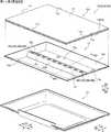
本発明の第1実施形態による表示装置10には、図1に示すように、表示装置本体10aが設けられている。表示装置本体10aは、後述する、画像を表示する表示部11と、反射シート12と、光学シート13と、リアフレーム14とを含む。表示部11は、たとえば、液晶セルからなり、映像を表示可能に構成されている。なお、以下の説明において、表示装置10の表示部11に対向する位置から見て、左方向を矢印X1方向、右方向を矢印X2方向、正面方向(手前方向)を矢印Y1方向、背面方向を矢印Y2方向、上方向を矢印Z1方向、下方向を矢印Z2方向として説明する。(Overall configuration of display device)
As shown in FIG. 1, the display device 10 according to the first embodiment of the present invention is provided with a display device
また、表示装置10は、表示部11に光を放射するLED素子100を備える。表示装置10は、矢印Y2方向側に設けられたLED(Light Emitting Diode)素子100をバックライトとして表示部11に映像を表示する直下型液晶モジュールとして構成されている。なお、LED素子100は、特許請求の範囲の「光源」の一例である。 Further, the display device 10 includes an
(表示装置の各部の構成)
図1に示すように、表示部11は、XZ平面に平行な面上に、板状に形成されている。また、表示部11は、短辺部11aおよび11bと、長辺部11cおよび11dとを含む、長方形形状を有するように構成されている。また、表示部11は、短辺部11a、短辺部11b、長辺部11c、および、長辺部11dによって取り囲まれる表示面11eを含む。(Configuration of each part of the display device)
As shown in FIG. 1, the
LED素子100は、LEDチップ100a(図3参照)を含む。LED素子100は、複数(たとえば、10個)設けられており、表示部11側(矢印Y1方向側)に光を照射するように構成されている。なお、LEDチップ100aは、特許請求の範囲の「半導体素子」の一例である。 The
反射シート12は、表示部11の表示面11eに略平行に配置される底面部12aを含む。なお、表示部11の表示面11eは光学シート13と略平行に配置されている。また、反射シート12は、底面部12aと表示部11の外縁部(短辺部11aおよび11b、長辺部11cおよび11d)との間に、底面部12aに対して傾斜して設けられる傾斜部12b〜12eとを含み、LED素子100からの光を反射(および拡散)するように構成されている。また、反射シート12は、リアフレーム14と光学シート13との間に設けられており、LED素子100からの光を、表示部11側(矢印Y1方向側)に反射するように構成されている。なお、リアフレーム14は、たとえば、金属により形成されており、矢印Y2方向に窪む凹形状に形成されている。また、リアフレーム14は、表示装置10に矢印Y2方向側から取り付けられている。 The
具体的には、反射シート12は、たとえば、樹脂(好ましくは、反射性を有する状態のPET(Polyethylene terepthalate))により形成されている。そして、反射シート12は、リアフレーム14に沿った形状(矢印Y2方向側に窪む凹形状)を有するように構成されている。 Specifically, the
反射シート12の底面部12aは、XZ平面に平行な平面上で、長方形形状を有するように形成されている。 The
反射シート12の傾斜部12b〜12eは、底面部12aの4辺を取り囲むように配置されている。傾斜部12bは、底面部12aの矢印X1方向側の端部と表示部11の短辺部11aとの間に設けられ、底面部12aに対して傾斜して設けられている。傾斜部12c(12d、および、12e)は、傾斜部12bと同様に、底面部12aの端部と表示部11の短辺部11b(長辺部11c、および、長辺部11d)との間に設けられ、底面部12aに対して傾斜して設けられている。 The
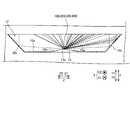
ここで、第1実施形態では、図1および図2に示すように、LED素子100は、表示部11の表示面11eに略垂直な方向(Y方向)において、底面部12aよりも表示部11に近い位置に配置されている。具体的には、表示装置10には、底面部12aから表示部11側(Y1方向側)に突出している光源配置部15が設けられている。 Here, in the first embodiment, as shown in FIGS. 1 and 2, the
光源配置部15は、傾斜部12dと対向するように設けられる傾斜部15aと、傾斜部12eと対向するように設けられる傾斜部15bを含む。また、光源配置部15は、傾斜部15aのY1方向側の端部と、傾斜部15bのY1方向側の端部とを接続する平坦部15cを含む。平坦部15cは、X方向に延びるように設けられている。平坦部15cには、10個のLED素子100が、X方向に互いに間隔を隔てて実装されている。なお、図示しないが、平坦部15cとLED素子100との間には光源用の基板およびヒートシンクが設けられている。また、光源配置部15は、反射シート12により覆われていてもよい。 The light
また、図2に示すように、光源配置部15の断面形状は、台形形状を有している。平坦部15c上に配置されたLED素子100は、放射状に光を放出する。なお、図2では、反射シート12、光源配置部15、および、LED素子100以外の部材は、簡略化のため、図示を省略している。また、図2の破線は、LED素子100から放出される光の経路の一例である。 Further, as shown in FIG. 2, the cross-sectional shape of the light
図1に示すように、光学シート13は、拡散板や偏光フィルタ等からなり、表示部11とリアフレーム14との間で、XZ平面に平行な平面に広がる平板状に形成されている。これにより、LED素子100から照射された光は、光学シート13に照射され、光学シート13により、拡散および偏光方向が揃えられる。なお、光学シート13は、1枚のシートとして構成されている場合に限らず、それぞれ所定の機能を有する複数枚のシートの組み合わせからなっていてもよい。 As shown in FIG. 1, the
そして、表示部11は、光学シート13を透過した光に対して、液晶の透過率を変化させることなどにより、画像の表示を行うように構成されている。 The
(LED素子の構成)
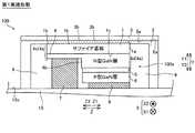
ここで、第1実施形態では、図3に示すように、LED素子100は、サファイア基板1を含むLEDチップ100aを備える。また、LED素子100は、LEDチップ100aを覆う透光性の封止樹脂2を含む。封止樹脂2の上面2aは略平坦に形成されている。また、LED素子100は、封止樹脂2の上面2aに配置される反射層3を備える。具体的には、封止樹脂2の上面2aは、光源配置部15の平坦部15cと略平行になるように形成されている。なお、サファイア基板1および上面2aは、それぞれ、特許請求の範囲の「基板」および「封止樹脂の上面」の一例である。なお、「上面2aが略平坦に形成されている」とは、封止樹脂2の上面2aに微細な凹凸が形成されている場合も含む広い概念である。(Configuration of LED element)
Here, in the first embodiment, as shown in FIG. 3, the
LEDチップ100a(後述するPN接合部5)から発光された光のうち、LEDチップ100aの上方側に発光された光は、反射層3に入射され、LEDチップ100aの側方側、または、反射層3の下方側に反射される。 Of the light emitted from the
また、反射層3の下面3aは凹凸形状を有する。具体的には、反射層3の下面3aには、複数の微細な突起部3bが配置されている。突起部3bは、矢印Y2方向側に向かって先細るように突出している。なお、下面3aは、特許請求の範囲の「反射層の下面」の一例である。 Further, the
また、サファイア基板1の上面1aは凹凸形状を有する。具体的には、サファイア基板1の上面1aには、複数の微細な突起部1bが配置されている。突起部1bは、矢印Y1方向側に突出している。なお、複数の突起部1bは、放電加工によって形成されている。なお、上面1aは、特許請求の範囲の「基板の上面」の一例である。 Further, the
また、反射層3は、金により形成されている。具体的には、反射層3は、封止樹脂2の上面2aに金を蒸着することによって設けられている。 Further, the
また、第1実施形態では、反射層3は、略平坦に形成されている。具体的には、反射層3は、Y方向の厚みが略一定になるように構成されている。なお、「反射層3は、略平坦に形成されている」とは、反射層3の下面3aに微細な凹凸が形成されている場合も含む広い概念である。 Further, in the first embodiment, the
また、第1実施形態では、LEDチップ100aは、封止樹脂2の上面2a側(矢印Y1方向側)から、サファイア基板1、N型GaN層4、PN接合部5、P型GaN層6の順に配置されるように構成されている。すなわち、LEDチップ100aは、サファイア基板1が最上面に配置される。すなわち、LEDチップ100aは、フリップチップ型である。具体的には、サファイア基板1の下面1cの下部にN型GaN層4が形成されている。また、N型GaN層4の下面4aには、X方向から見て、Y方向に延びる段差部4bが設けられている。N型GaN層4の下面4aには、段差部4bを境に、X1方向側に略平坦な平坦面4cと、X2方向側に略平坦な平坦面4dとが設けられている。PN接合部5は、N型GaN層4の平坦面4dの下部に形成されている。また、N型GaN層4の平坦面4cの下部には、負電極パッド7が設けられている。また、P型GaN層6の下部には、正電極パッド8が設けられている。また、正電極パッド8および負電極パッド7は、光源配置部15の平坦部15c上の図示しない銅箔と接触している(半田付けされている)とともに、電気的に接続されている。なお、PN接合部5は、特許請求の範囲の「発光層」の一例である。また、N型GaN層4、および、P型GaN層6は、それぞれ、特許請求の範囲の「第1導電型GaN層」および「第2導電型GaN層」の一例である。 Further, in the first embodiment, the
また、第1実施形態では、図4に示すように、平面視において、反射層3の外周は、LEDチップ100aの外周よりも外側に配置されている。具体的には、平面視において、反射層3は、短辺部3c(矢印Z2方向側)および3d(矢印Z1方向側)と、長辺部3e(矢印X1方向側)および3f(矢印X2方向側)とを含む、長方形形状を有するように構成されている。また、平面視において、サファイア基板1は、短辺部1d(矢印Z2方向側)および1e(矢印Z1方向側)と、長辺部1f(矢印X1方向側)および1g(矢印X2方向側)とを含む、長方形形状を有するように構成されている。また、反射層3の短辺部3cは、サファイア基板1の短辺部1dよりも矢印Z2方向側に設けられているとともに、反射層3の短辺部3dは、サファイア基板1の短辺部1eよりも矢印Z1方向側に設けられている。また、反射層3の長辺部3eは、サファイア基板1の長辺部1fよりも矢印X1方向側に設けられているとともに、反射層3の長辺部3fは、サファイア基板1の長辺部1gよりも矢印X2方向側に設けられている。なお、短辺部3c、短辺部3d、長辺部3e、および、長辺部3fは、それぞれ、「反射層の外周」の一例である。また、短辺部1d、短辺部1e、長辺部1f、および、長辺部1gは、それぞれ、「半導体素子の外周」の一例である。 Further, in the first embodiment, as shown in FIG. 4, the outer circumference of the
また、平面視において、反射層3の外周は、封止樹脂2(図3参照)の外周と略重なるように構成されている。具体的には、平面視において、封止樹脂2は、短辺部2b(矢印Z2方向側)および2c(矢印Z1方向側)と、長辺部2d(矢印X1方向側)および2e(矢印X2方向側)とを含む、長方形形状を有するように構成されている。また、平面視において、反射層3の短辺部3cと、封止樹脂2の短辺部2bとは略重なっている。また、平面視において、反射層3の短辺部3dと、封止樹脂2の短辺部2cとは略重なっている。また、平面視において、反射層3の長辺部3eと、封止樹脂2の長辺部2dとは略重なっている。また、平面視において、反射層3の長辺部3fと、封止樹脂2の長辺部2eとは略重なっている。 Further, in a plan view, the outer circumference of the
また、第1実施形態では、図3に示すように、サファイア基板1の上面1aと反射層3の下面3aとは、封止樹脂2を介して離間するように構成されている。具体的には、サファイア基板1の上面1aの全体は、封止樹脂2によって覆われている。 Further, in the first embodiment, as shown in FIG. 3, the
また、第1実施形態では、封止樹脂2とLEDチップ100aとの間に配置される蛍光体層9をさらに備える。蛍光体層9は、LEDチップ100aの側面に配置されている。また、蛍光体層9は、平面視において反射層3と重なるように配置されている。また、封止樹脂2とLEDチップ100a(サファイア基板1)の上面1aとは密着するように構成されている。具体的には、蛍光体層9は、サファイア基板1の上面1a以外のLEDチップ100aの表面全体を覆うように配置されている。また、蛍光体層9の全体は、封止樹脂2の内部に配置されている。 Further, in the first embodiment, the
また、第1実施形態では、図4に示すように、蛍光体層9は、LEDチップ100aの側面を取り囲むように配置されている。具体的には、平面視において、LEDチップ100a(サファイア基板1)の短辺部1d、短辺部1e、長辺部1f、および、長辺部1gの各々と密着するように、厚みt1の蛍光体層9が配置されている。 Further, in the first embodiment, as shown in FIG. 4, the
(第1実施形態の効果)
第1実施形態では、以下のような効果を得ることができる。(Effect of the first embodiment)
In the first embodiment, the following effects can be obtained.
第1実施形態では、上記のように、画像を表示する表示部11と、表示部11に光を放射するLED素子100と、を備え、LED素子100は、サファイア基板1を含むLEDチップ100aと、LEDチップ100aを覆う透光性の封止樹脂2と、封止樹脂2の上面2aに配置される反射層3と、を含むように、表示装置10を構成する。これにより、反射層3が、LEDチップ100aを覆うように設けられている封止樹脂2の上面2aに配置されているので、反射層3の面積(平面積)をLEDチップ100aの面積(平面積)よりも容易に大きくすることができる。その結果、反射層3の面積(平面積)がLEDチップ100aの面積(平面積)と略等しい場合に比べて、LEDチップ100aからLEDチップ100aの上方側に発光された光が、反射層3によってLEDチップ100aの側方側に反射される割合が増加する。これにより、LED素子100の上方側へ発光される光に対して、LED素子100の側方側へ発光される光の割合を増加させることができるので、LED素子100からの光の配光角度の低下を抑制することができる。また、反射層3とLEDチップ100aとを別体として設けることによって、LEDチップ100aの発熱等の影響を考慮する必要がないので、反射層3の材質の選択範囲を広げることができる。また、反射層3を封止樹脂2上に設けることによって、反射層3とLEDチップ100aとを一体的に設ける場合に比べて、容易に反射層3を形成することができる。なお、「上面2aが略平坦に形成されている」とは、封止樹脂2の上面2aに微細な凹凸が形成されている場合も含む広い概念である。 In the first embodiment, as described above, the
また、第1実施形態では、上記のように、平面視において、反射層3の外周が、LEDチップ100aの外周よりも外側に配置されているように、表示装置10を構成する。これにより、平面視において、反射層3が占める領域がLEDチップ100aが占める領域全体を覆うとともに、反射層3の面積がLEDチップ100aの面積よりも大きくなる。その結果、LEDチップ100aからLEDチップ100aの上方側に発光された光を、反射層3によってLEDチップ100aの側方の4方全てに容易に反射させることができる。これにより、LED素子100の上方側へ発光される光に対して、LED素子100の側方側へ発光される光の割合をさらに増加させることができるので、LED素子100からの光の配光角度の低下をさらに抑制することができる。 Further, in the first embodiment, as described above, the display device 10 is configured so that the outer circumference of the
また、第1実施形態では、上記のように、平面視において、反射層3の外周が、封止樹脂2の外周と略重なるように、表示装置10を構成する。これにより、封止樹脂2の端辺の近傍を通過する光を反射層3によって反射させることができるので、LEDチップ100aからの光をLED素子100の側方側へ容易に反射させることができる。 Further, in the first embodiment, as described above, the display device 10 is configured so that the outer circumference of the
また、第1実施形態では、上記のように、LEDチップ100aが、サファイア基板1が最上面に配置され、サファイア基板1の上面1aと反射層3の下面3aとが、封止樹脂2を介して離間するように、表示装置10を構成する。これにより、反射層3が、サファイア基板1の側方の封止樹脂2の上面2aとサファイア基板1の上面1aとの両方に跨るように、封止樹脂2の高さを調節する必要がないので、容易にLED素子100を形成することができる。また、サファイア基板1と反射層3とが干渉しないので、サファイア基板1および反射層3の劣化を抑制することができる。 Further, in the first embodiment, as described above, the
また、第1実施形態では、上記のように、封止樹脂2とLEDチップ100aとの間に配置される蛍光体層9をさらに備え、蛍光体層9が、LEDチップ100aの側面に配置されるとともに、平面視において、反射層3と重なるように配置されており、封止樹脂2とLEDチップ100a(サファイア基板1)の上面1aとが密着するように、表示装置10を構成する。これにより、LEDチップ100a(サファイア基板1)の上面1aには蛍光体層9が配置されず、LEDチップ100aの側面にのみ蛍光体層9が配置されることによって、LED素子100の高さを小さくすることができる。 Further, in the first embodiment, as described above, the
また、第1実施形態では、上記のように、蛍光体層9が、LEDチップ100aの側面を取り囲むように配置されている、表示装置10を構成する。これにより、LEDチップ100aの側面側から進む光を、容易に蛍光体層9に導入させることができる。 Further, in the first embodiment, as described above, the display device 10 is configured in which the
また、第1実施形態では、上記のように、反射層3の下面3aが凹凸形状を有するように、表示装置10を構成する。これにより、LEDチップ100aから発光され、反射層3の下面3aに入射した光が、反射層3の凹凸によって拡散されるので、LEDチップ100aの側方側へ反射される光の割合を効果的に増加させることができる。 Further, in the first embodiment, as described above, the display device 10 is configured so that the
また、第1実施形態では、上記のように、サファイア基板1の上面1aが凹凸形状を有するように、表示装置10を構成する。これにより、LEDチップ100aから発光される光がサファイア基板1の凹凸によって拡散されるので、LED素子100の側方側へ発光される光の割合を効果的に増加させることができる。 Further, in the first embodiment, as described above, the display device 10 is configured so that the
また、第1実施形態では、上記のように、反射層3が、金を含むように、表示装置10を構成する。ここで、金は熱または湿度に対して耐性(耐熱性および耐食性)が優れている。したがって、反射層3が金を含むことによって、反射層3の熱または湿度に対する耐性(耐熱性および耐食性)を向上させることができる。 Further, in the first embodiment, as described above, the display device 10 is configured so that the
また、第1実施形態では、上記のように、反射層3が、略平坦に形成されているように、表示装置10を構成する。これにより、反射層3を容易に形成することができる。 Further, in the first embodiment, the display device 10 is configured so that the
また、第1実施形態では、上記のように、基板が、サファイア基板1を含み、LEDチップ100aが、封止樹脂2の上面2a側から、サファイア基板1、N型GaN層4、PN接合部5、P型GaN層6の順に配置されるように、表示装置10を構成する。ここで、サファイア基板1は、光透過性に優れている。したがって、基板がサファイア基板1を含むことによって、基板によって吸収される光の割合を低下させることができるので、LED素子100の発光効率の低下を抑制することができる。 Further, in the first embodiment, as described above, the substrate includes the
また、第1実施形態では、上記のように、表示装置本体10aの背面側に配置されるLEDチップ100aを備え、LEDチップ100aが、封止樹脂2により覆われているとともに、封止樹脂2の上面2aには、反射層3が配置されており、LEDチップ100aから照射される光が反射層3によって反射されるように、表示装置10を構成する。これにより、反射層3が、LEDチップ100aを覆うように設けられている封止樹脂2の上面2aに配置されているので、反射層3の面積(平面積)をLEDチップ100aの面積(平面積)よりも容易に大きくすることができる。その結果、反射層3の面積(平面積)がLEDチップ100aの面積(平面積)と略等しい場合に比べて、LEDチップ100aからLEDチップ100aの上方側に発光された光が、反射層3によってLEDチップ100aの側方側に反射される割合が増加する。これにより、LED素子100の上方側へ発光される光に対して、LED素子100の側方側へ発光される光の割合を増加させることができるので、LED素子100からの光の配光角度の低下を抑制することができる。その結果、LED素子100による光の照射範囲を広くすることができるので、表示装置本体10aの表示部11において、輝度のムラが発生するのを抑制することができる。 Further, in the first embodiment, as described above, the
また、第1実施形態では、上記のように、LED素子100が、表示部11の表示面11eに略垂直な方向において、底面部12aよりも表示部11に近い位置に配置されるように、表示装置10を構成する。これにより、LED素子100が底面部12a上に配置される場合に比べて、LED素子100と表示部11との間の距離が小さくなるので、LED素子100からの光をより効率的に表示部11に伝えることができる。 Further, in the first embodiment, as described above, the
[参考例]
次に、図5および図6を参照して、参考例による表示装置20の構成について説明する。この参考例における表示装置20は、サファイア基板1と反射層3とが離間しているLED素子100を備える第1実施形態の表示装置10とは異なり、サファイア基板1と反射層3とが密着しているLED素子200を備える。なお、図中において上記第1実施形態と同様の構成の部分には、同一の符号を付している。[Reference example ]
Next, the configuration of the display device 20 accordingto the reference example will be described with reference to FIGS. 5 and 6. Thedisplay device 20 in this reference example is different from the display device 10 of the first embodiment in which the
参考例では、図5に示すように、サファイア基板1の上面1aと、反射層3の下面3aとが密着するように構成されている。具体的には、サファイア基板1の上面1aと、反射層3の下面3aとの間には、封止樹脂2が介在していない。In the reference example , as shown in FIG. 5, the
また、図6に示すように、平面視において、LEDチップ100a(サファイア基板1)の短辺部1d、短辺部1e、長辺部1f、および、長辺部1gの各々と密着するように、厚みt2の蛍光体層19が配置されている。なお、厚みt2は、厚みt1(図4参照)よりも小さい。 Further, as shown in FIG. 6, in a plan view, the
参考例のその他の構成は、上記第1実施形態と同様である。Other configurations of the reference example are the same as those of the first embodiment.
(参考例の効果)
参考例では、上記のように、LEDチップ100aが、サファイア基板1が最上面に配置され、サファイア基板1の上面1aと、反射層3の下面3aとが密着するように、表示装置20を構成する。これにより、サファイア基板1の上面1aと反射層3の下面3aとの間に封止樹脂2が介在しないことによって、LEDチップ100aから上方側へ発光される光が封止樹脂2によって吸収されるのを抑制することができる。その結果、LED素子200の発光効率の低下を抑制することができる。(Effect ofreference example)
In the reference example , as described above, the display device 20 is configured such that the
なお、参考例のその他の効果は、上記第1実施形態と同様である。The other effects of the reference example are the same as those of the first embodiment.
[参考例]
次に、図1および図7を参照して、参考例による表示装置30の構成について説明する。この参考例における表示装置30では、蛍光体層9が設けられているLED素子100を備える第1実施形態とは異なり、LED素子300には蛍光体層9が設けられていない。なお、図中において上記第1実施形態と同様の構成の部分には、同一の符号を付している。[Reference example]
Next, the configuration of the display device 30 according to the reference example will be described with reference to FIGS. 1 and 7. In the display device 30 in this reference example, unlike the first embodiment including the
参考例では、図7に示すように、封止樹脂2とLEDチップ100aの側面とは密着するように構成されている。具体的には、封止樹脂2とLEDチップ100aの側面との間には蛍光体層9が介在されていない。詳細には、表示装置30は、LEDチップ100aから発光された光が、量子ドットを含む光学シート23(図1参照)に入射されることによって、色が変化するように構成されている。In the reference example , as shown in FIG. 7, the sealing
参考例のその他の構成は、上記第1実施形態と同様である。Other configurations of the reference example are the same as those of the first embodiment.
(参考例の効果)
参考例では、以下のような効果を得ることができる。(Effect ofreference example)
In the reference example , the following effects can be obtained.
参考例では、上記のように、封止樹脂2とLEDチップ100aの側面とが密着するように、表示装置30を構成する。これにより、LEDチップ100aの側面側に蛍光体層9などを設ける場合と異なり、LED素子300を小型化させることができる。In the reference example , the display device 30 is configured so that the sealing
なお、参考例のその他の効果は、上記第1実施形態と同様である。The other effects of the reference example are the same as those of the first embodiment.
[第2実施形態]
次に、図8および図9を参照して、第2実施形態による表示装置40の構成について説明する。この第2実施形態における表示装置40では、第1実施形態とは異なり、LED素子400の反射層33にパターンが形成されている。なお、図中において上記第1実施形態と同様の構成の部分には、同一の符号を付している。なお、LED素子400は、特許請求の範囲の「光源」の一例である。[Second Embodiment]
Next, the configuration of the display device 40 according tothe second embodiment will be described with reference to FIGS. 8 and 9. In thedisplay device 40 of the second embodiment, unlike the first embodiment, a pattern is formed on the
第2実施形態では、図8に示すように、反射層33は、LEDチップ100aからの光の一部を透過する所定のパターンを含む。具体的には、反射層33の一部が除去されることにより溝部33aが形成されており、溝部33aから封止樹脂2が露出している。In thesecond embodiment, as shown in FIG. 8, the
また、第2実施形態では、図9に示すように、所定のパターンは、長方形をZ方向に並べた形状を有する。具体的には、平面視において、溝部33aは、封止樹脂2の長辺部2dから長辺部2eまでX方向に延びている。詳細には、平面視において、反射層33と溝部33aとが交互に連続して配列されるように構成されている。なお、Z方向は、特許請求の範囲の「所定方向」の一例である。Further, in thesecond embodiment, as shown in FIG. 9, the predetermined pattern has a shape in which rectangles are arranged in the Z direction. Specifically, in a plan view, the
第2実施形態のその他の構成は、上記第1実施形態と同様である。Other configurations of thesecond embodiment are the same as those of the first embodiment.
(第2実施形態の効果)
第2実施形態では、以下のような効果を得ることができる。(Effect ofthe second embodiment)
In thesecond embodiment, the following effects can be obtained.
第2実施形態では、上記のように、反射層33が、LEDチップ100aからの光の一部を透過する所定のパターンを含むように、表示装置40を構成する。これにより、LEDチップ100aからの光の一部を、反射層33のパターン(パターンの隙間)を介してLED素子400の外部へ透過させることによって利用することができる。In thesecond embodiment, as described above, the display device 40 is configured so that the
第2実施形態では、上記のように、所定のパターンが、長方形をZ方向に並べた形状を有するように、表示装置40を構成する。これにより、LEDチップ100aからの光の一部を、LED素子400の外部へ容易に透過させることができる。In thesecond embodiment, as described above, the display device 40 is configured so that the predetermined pattern has a shape in which rectangles are arranged in the Z direction. As a result, a part of the light from the
なお、第2実施形態のその他の効果は、上記第1実施形態と同様である。The other effects of thesecond embodiment are the same as those of the first embodiment.
[変形例]
なお、今回開示された実施形態は、すべての点で例示であって制限的なものではないと考えられるべきである。本発明の範囲は、上記した実施形態の説明ではなく特許請求の範囲によって示され、さらに特許請求の範囲と均等の意味および範囲内でのすべての変更(変形例)が含まれる。[Modification example]
It should be noted that the embodiments disclosed this time are exemplary in all respects and are not considered to be restrictive. The scope of the present invention is shown by the scope of claims rather than the description of the above-described embodiment, and further includes all modifications (modifications) within the meaning and scope equivalent to the scope of claims.
たとえば、上記第1実施形態では、LEDチップ100aが、サファイア基板1が最上面に配置されるフリップチップ型である例を示したが、本発明はこれに限られない。たとえば、図10に示すように、LEDチップ100aが、サファイア基板1が最下面に配置されるラテラルチップ型であってもよい。この場合、負電極パッド7および正電極パッド8の各々は、ワイヤ(図示せず)を介して、光源配置部15の平坦部15c上の銅箔(図示せず)に接続される。また、第2〜第4実施形態においても、LEDチップ100aがラテラルチップ型であってもよい。 For example, in the first embodiment, the
また、上記第1および2実施形態では、光源が、LED素子100(200、300、400)である例を示したが、本発明はこれに限られない。たとえば、光源が、LED素子以外の素子であってもよい。Further, in the firstand second embodiments, the light source is the LED element 100 (200, 300, 400), but the present invention is not limited to this. For example, the light source may be an element other than the LED element.
また、上記第2実施形態では、反射層33が、長方形をZ方向に並べた形状を有する例を示したが、本発明はこれに限られない。たとえば、反射層33が、格子形状を有していてもよい。Further, in thesecond embodiment, the example in which the
また、上記第1および第2実施形態では、蛍光体層9が、LEDチップ100aの側面にのみ配置されている構成の例を示したが、本発明はこれに限られない。たとえば、蛍光体層9が、LEDチップ100a(サファイア基板1)の上面1aにも設けられていてもよい。Further, in the first andsecond embodiments, the example of the configuration in which the
また、上記第1および第2実施形態では、サファイア基板1の上面1aが凹凸形状を有している構成の例を示したが、本発明はこれに限られない。たとえば、サファイア基板1の下面1cが凹凸形状を有していてもよい。また、サファイア基板1の上面1aおよび下面1cの各々が凹凸形状を有していてもよい。Further, in the firstand second embodiments, an example of a configuration in which the
また、上記第1および第2実施形態では、反射層3(33)が金により形成されている例を示したが、本発明はこれに限られない。たとえば、反射層3(33)が銀により形成されていてもよい。Further, in the firstand second embodiments, the example in which the reflective layer 3 (33) is formed of gold is shown, but the present invention is not limited to this. For example, the reflective layer 3 (33) may be made of silver.
また、上記第1および第2実施形態では、平面視において、反射層3(33)(LED素子100(200、300、400))、および、サファイア基板1(LEDチップ100a)の各々が長方形形状を有する構成の例を示したが、本発明はこれに限られない。たとえば、反射層3(33)(LED素子100(200、300、400))、および、サファイア基板1(LEDチップ100a)の各々が正方形形状を有する構成であってもよい。Further, in the firstand second embodiments, the reflective layer 3 (33) (LED element 100 (200, 300, 400)) and the sapphire substrate 1 (
また、上記第1および第2実施形態では、突起部1b(突起部3b)が、矢印Y1(Y2)方向側に先細るように突出している構成の例を示したが、本発明はこれに限られない。たとえば、突起部1b(突起部3b)が、球面状に構成されていてもよい。Further, in the firstand second embodiments, an example of a configuration in which the
1 サファイア基板(基板)
1a 上面(基板の上面)
1d、1e 短辺部(半導体素子の外周)
1f、1g 長辺部(半導体素子の外周)
2 封止樹脂
2a 上面(封止樹脂の上面)
3、33 反射層
3a 下面(反射層の下面)
3c、3d 短辺部(反射層の外周)
3e、3f 長辺部(反射層の外周)
4 N型GaN層(第1導電型GaN層)
5 PN接合部(発光層)
6 P型GaN層(第2導電型GaN層)
9、19 蛍光体層
10、20、30、40 表示装置
11 表示部
11e 表示面
12 反射シート
12a 底面部
100、200、300、400 LED素子(光源)
100a LEDチップ(半導体素子)
Z 方向(所定方向)1 Sapphire board (board)
1a Top surface (upper surface of substrate)
1d, 1e Short side (outer circumference of semiconductor element)
1f, 1g Long side (outer circumference of semiconductor element)
2 Encapsulating
3, 33
3c, 3d short side (outer circumference of reflective layer)
3e, 3f Long side (outer circumference of reflective layer)
4 N-type GaN layer (first conductive type GaN layer)
5 PN junction (light emitting layer)
6 P-type GaN layer (second conductive type GaN layer)
9, 19 Fluorescent layer 10, 20, 30, 40
100a LED chip (semiconductor element)
Z direction (predetermined direction)
Claims (9)
Translated fromJapanese前記表示部に光を放射する光源と、を備え、
前記光源は、基板を含む半導体素子と、
前記半導体素子を覆う透光性の封止樹脂と、
前記封止樹脂の上面に配置される反射層と、
前記封止樹脂と前記半導体素子との間に配置される蛍光体層と、を含み、
前記蛍光体層は、前記半導体素子の側面に配置されるとともに、平面視において、前記反射層と重なるように配置されており、
前記封止樹脂と前記半導体素子の上面とは密着するように構成されている、表示装置。A display unit that displays images and
The display unit is provided with a light source that emits light.
The light source includes a semiconductor element including a substrate and
A translucent sealing resin that covers the semiconductor element,
A reflective layer arranged on the upper surface of the sealing resin and
A phosphor layer arranged between the sealing resin and the semiconductor element is included.
The phosphor layer is arranged on the side surface of the semiconductor element and is arranged so as tooverlap the reflective layer in a plan view.
A display deviceconfigured so that the sealing resin and the upper surface of the semiconductor element are in close contact with each other.
前記基板の上面と前記反射層の下面とは、前記封止樹脂を介して離間するように構成されている、請求項1または2に記載の表示装置。In the semiconductor element, the substrate is arranged on the uppermost surface, and the substrate is arranged on the uppermost surface.
The display device according to claim 1 or 2, wherein the upper surface of the substrate and the lower surface of the reflective layer are configured to be separated from each other via the sealing resin.
前記半導体素子は、前記封止樹脂の前記上面側から、前記サファイア基板、第1導電型GaN層、発光層、第2導電型GaN層の順に配置されるように構成されている、請求項1〜7のいずれか1項に記載の表示装置。The substrate includes a sapphire substrate.
The semiconductor element is configured so that the sapphire substrate, the first conductive type GaN layer, the light emitting layer, and the second conductive type GaN layer are arranged in this order from the upper surface side of the sealing resin. The display device according to any one of7 to 7.
前記反射シートは、前記表示部の表示面に略平行に配置される底面部を含み、
前記光源は、前記表示部の表示面に略垂直な方向において、前記底面部よりも前記表示部に近い位置に配置されている、前記請求項1〜8のいずれか1項に記載の表示装置。Further provided with a reflective sheet that reflects light from the light source,
The reflective sheet includes a bottom surface portion that is arranged substantially parallel to the display surface of the display unit.
The display device according to any one ofclaims 1 to 8 , wherein the light source is arranged at a position closer to the display unit than the bottom surface portion in a direction substantially perpendicular to the display surface of the display unit. ..
Priority Applications (10)
| Application Number | Priority Date | Filing Date | Title |
|---|---|---|---|
| JP2016210490AJP6932910B2 (en) | 2016-10-27 | 2016-10-27 | Display device |
| US15/793,088US10522726B2 (en) | 2016-10-27 | 2017-10-25 | Display device |
| CN201711013273.XACN108008570B (en) | 2016-10-27 | 2017-10-26 | Display device |
| CN201811593740.5ACN110082952A (en) | 2016-10-27 | 2017-10-26 | Display device |
| CN202011299750.5ACN112327541A (en) | 2016-10-27 | 2017-10-26 | Light source |
| EP17198757.1AEP3316027B1 (en) | 2016-10-27 | 2017-10-27 | Display device |
| EP20208450.5AEP3800674A1 (en) | 2016-10-27 | 2017-10-27 | Light source |
| EP19151492.6AEP3489744B1 (en) | 2016-10-27 | 2017-10-27 | Display device |
| US16/240,079US10854799B2 (en) | 2016-10-27 | 2019-01-04 | Display device |
| US17/085,368US11538971B2 (en) | 2016-10-27 | 2020-10-30 | Light source |
Applications Claiming Priority (1)
| Application Number | Priority Date | Filing Date | Title |
|---|---|---|---|
| JP2016210490AJP6932910B2 (en) | 2016-10-27 | 2016-10-27 | Display device |
Publications (2)
| Publication Number | Publication Date |
|---|---|
| JP2018073933A JP2018073933A (en) | 2018-05-10 |
| JP6932910B2true JP6932910B2 (en) | 2021-09-08 |
Family
ID=60190691
Family Applications (1)
| Application Number | Title | Priority Date | Filing Date |
|---|---|---|---|
| JP2016210490AActiveJP6932910B2 (en) | 2016-10-27 | 2016-10-27 | Display device |
Country Status (4)
| Country | Link |
|---|---|
| US (3) | US10522726B2 (en) |
| EP (3) | EP3316027B1 (en) |
| JP (1) | JP6932910B2 (en) |
| CN (3) | CN112327541A (en) |
Families Citing this family (5)
| Publication number | Priority date | Publication date | Assignee | Title |
|---|---|---|---|---|
| JP7341057B2 (en)* | 2017-07-13 | 2023-09-08 | ソニーグループ株式会社 | Light emitting devices, display devices and lighting devices |
| JP7116320B2 (en)* | 2019-04-24 | 2022-08-10 | 日亜化学工業株式会社 | light emitting device |
| CN110600598B (en)* | 2019-08-21 | 2021-02-05 | 苏州紫灿科技有限公司 | Inverted ultraviolet LED with double-layer nano array structure and preparation method |
| US12419720B2 (en) | 2021-04-26 | 2025-09-23 | Springloc Ltd. | Multimodality ID markers for delineating the position of a region of interest (ROI) within a body |
| US12402976B2 (en) | 2021-04-26 | 2025-09-02 | Springloc Ltd | Augmented reality soft tissue biopsy and surgery system |
Family Cites Families (57)
| Publication number | Priority date | Publication date | Assignee | Title |
|---|---|---|---|---|
| CN1196203C (en)* | 1999-07-29 | 2005-04-06 | 西铁城电子股份有限公司 | led |
| CN2388710Y (en)* | 1999-08-18 | 2000-07-19 | 亿光电子工业股份有限公司 | Color-mixing LED device |
| JP2001257381A (en)* | 2000-03-13 | 2001-09-21 | Sharp Corp | Light emitting diode, method of manufacturing the same, and lighting device |
| AT410266B (en) | 2000-12-28 | 2003-03-25 | Tridonic Optoelectronics Gmbh | LIGHT SOURCE WITH A LIGHT-EMITTING ELEMENT |
| JP2004055772A (en)* | 2002-07-18 | 2004-02-19 | Citizen Electronics Co Ltd | LED light emitting device |
| JP4503950B2 (en)* | 2003-07-11 | 2010-07-14 | スタンレー電気株式会社 | Method for manufacturing phosphor-integrated LED lamp |
| US7791274B2 (en)* | 2004-01-07 | 2010-09-07 | Panasonic Corporation | LED lamp |
| JP4357311B2 (en) | 2004-02-04 | 2009-11-04 | シチズン電子株式会社 | Light emitting diode chip |
| CN100345315C (en)* | 2004-03-12 | 2007-10-24 | 友达光电股份有限公司 | Light source module |
| JP4535792B2 (en)* | 2004-07-01 | 2010-09-01 | Nec液晶テクノロジー株式会社 | Backlight and liquid crystal display device including the backlight |
| KR100754169B1 (en)* | 2004-11-24 | 2007-09-03 | 삼성전자주식회사 | Side light emitting device, backlight unit using same as light source, and liquid crystal display device employing same |
| WO2006061763A1 (en)* | 2004-12-09 | 2006-06-15 | Koninklijke Philips Electronics N.V. | Illumination system |
| JP2006237217A (en)* | 2005-02-24 | 2006-09-07 | Toshiba Discrete Technology Kk | Semiconductor light emitting device and surface light emitting device |
| KR100638874B1 (en)* | 2005-07-06 | 2006-10-27 | 삼성전기주식회사 | A light source-light guide plate structure of a backlight device having an LED light source inserted into the light guide plate and a backlight device including the same |
| KR101225326B1 (en)* | 2005-08-08 | 2013-01-23 | 엘지디스플레이 주식회사 | Backlight assembly and liquid crystal display device having the same |
| CN1925176A (en)* | 2005-09-02 | 2007-03-07 | 杨丕福 | Integrated light emitting device and method for making same |
| US7293908B2 (en)* | 2005-10-18 | 2007-11-13 | Goldeneye, Inc. | Side emitting illumination systems incorporating light emitting diodes |
| US7868967B2 (en)* | 2005-10-27 | 2011-01-11 | Sharp Kabushiki Kaisha | Light source device, and display device and television receiver therewith |
| KR100732845B1 (en)* | 2005-11-17 | 2007-06-27 | 이승호 | Planar light emitting device for TFT-LCD using carbon nanotube |
| US7375379B2 (en)* | 2005-12-19 | 2008-05-20 | Philips Limileds Lighting Company, Llc | Light-emitting device |
| US7626210B2 (en) | 2006-06-09 | 2009-12-01 | Philips Lumileds Lighting Company, Llc | Low profile side emitting LED |
| TWI334050B (en)* | 2006-07-21 | 2010-12-01 | Coretronic Corp | Backlight module |
| CN101140976A (en)* | 2006-08-03 | 2008-03-12 | 丰田合成株式会社 | Light emitting device, method of making the same, and light source device comprising the same |
| CN101501875A (en)* | 2006-08-24 | 2009-08-05 | 夏普株式会社 | Light emitting element, light emitting element array, backlight unit, and liquid crystal display device |
| US7940380B1 (en) | 2007-01-23 | 2011-05-10 | Benner Jr William R | Rotary position detector and associated methods |
| KR101098859B1 (en)* | 2007-02-21 | 2011-12-26 | 울박, 인크 | Display device, apparatus for manufacturing display device, and method for manufacturing display device |
| JP2008218610A (en)* | 2007-03-02 | 2008-09-18 | Citizen Electronics Co Ltd | Light emitting diode |
| EP2216834B1 (en)* | 2007-11-29 | 2017-03-15 | Nichia Corporation | Light-emitting apparatus |
| KR101047718B1 (en)* | 2008-11-26 | 2011-07-08 | 엘지이노텍 주식회사 | Light emitting element |
| US20120013811A1 (en) | 2009-04-03 | 2012-01-19 | Sharp Kabushiki Kaisha | Lighting device, display device and television receiver |
| CN101867007A (en)* | 2010-05-11 | 2010-10-20 | 电子科技大学 | Preparation method of LED lamp phosphor layer |
| US20120113621A1 (en) | 2010-11-10 | 2012-05-10 | Taiwan Semiconductor Manufacturing Company, Ltd. | Batwing beam based led and backlight module using the same |
| JP5449274B2 (en)* | 2011-03-25 | 2014-03-19 | シャープ株式会社 | Lighting device and display device |
| JP5666962B2 (en)* | 2011-03-28 | 2015-02-12 | 日東電工株式会社 | Light emitting diode device and manufacturing method thereof |
| KR20120112997A (en)* | 2011-04-04 | 2012-10-12 | 엘지디스플레이 주식회사 | Light-emitting device package and a backlight unit having the same |
| WO2013038802A1 (en) | 2011-09-13 | 2013-03-21 | シャープ株式会社 | Surface light emitting device and liquid crystal display device provided with same |
| US8899771B2 (en)* | 2011-11-30 | 2014-12-02 | Sharp Kabushiki Kaisha | Illumination device, display device, and television reception device |
| JP5817521B2 (en)* | 2011-12-28 | 2015-11-18 | 日亜化学工業株式会社 | Method for manufacturing light emitting device |
| JP2013149711A (en)* | 2012-01-18 | 2013-08-01 | Citizen Holdings Co Ltd | Semiconductor light-emitting device |
| DE102012102114B4 (en) | 2012-03-13 | 2021-09-16 | OSRAM Opto Semiconductors Gesellschaft mit beschränkter Haftung | Radiation-emitting semiconductor component, lighting device and display device |
| US8833958B2 (en)* | 2012-04-13 | 2014-09-16 | Shenzhen China Star Optoelectronics Technology Co., Ltd. | Direct backlight module |
| US9140931B2 (en) | 2012-04-18 | 2015-09-22 | Shenzhen China Star Optoelectronics Technology Co., Ltd. | Backlight module and liquid crystal display device |
| CN202647490U (en)* | 2012-07-24 | 2013-01-02 | 京东方科技集团股份有限公司 | Backlight module and display device |
| TWI559053B (en) | 2013-05-28 | 2016-11-21 | 潘宇翔 | Light source device suitable for direct type backlight module and display thereof |
| KR101447437B1 (en) | 2013-07-29 | 2014-10-08 | 엘지디스플레이 주식회사 | Cover bottom and display apparatus using the same |
| KR102088148B1 (en)* | 2013-07-31 | 2020-03-13 | 삼성디스플레이 주식회사 | Display device |
| JP2015203724A (en)* | 2014-04-11 | 2015-11-16 | 船井電機株式会社 | display device |
| CN104235662A (en)* | 2014-08-21 | 2014-12-24 | 合肥鑫晟光电科技有限公司 | Light strip, backlight source and display device |
| CN204405995U (en)* | 2014-09-12 | 2015-06-17 | 康佳集团股份有限公司 | A kind of direct-light type LED backlight module and liquid crystal display |
| WO2016048971A1 (en)* | 2014-09-23 | 2016-03-31 | Koninklijke Philips N.V. | Luminance pattern shaping using a back-emitting led and a reflective substrate |
| CN104266116B (en)* | 2014-10-09 | 2017-03-15 | 深圳市华星光电技术有限公司 | A kind of backing structure and LCDs |
| TWI649900B (en)* | 2015-02-04 | 2019-02-01 | 億光電子工業股份有限公司 | LED package structure and manufacturing method thereof |
| JP6478155B2 (en) | 2015-05-13 | 2019-03-06 | パナソニックIpマネジメント株式会社 | Packing material |
| JP2017079311A (en)* | 2015-10-22 | 2017-04-27 | 豊田合成株式会社 | Manufacturing method for light-emitting device |
| CN105278163B (en)* | 2015-11-16 | 2019-01-22 | 深圳市华星光电技术有限公司 | A kind of down straight aphototropism mode set and display device |
| EP3460860A4 (en)* | 2016-05-20 | 2020-02-12 | Kabushiki Kaisha Toshiba | WHITE LIGHT SOURCE |
| CN205665499U (en)* | 2016-06-07 | 2016-10-26 | 京东方科技集团股份有限公司 | Light -emitting component , backlight unit and display device |
- 2016
- 2016-10-27JPJP2016210490Apatent/JP6932910B2/enactiveActive
- 2017
- 2017-10-25USUS15/793,088patent/US10522726B2/enactiveActive
- 2017-10-26CNCN202011299750.5Apatent/CN112327541A/enactivePending
- 2017-10-26CNCN201711013273.XApatent/CN108008570B/enactiveActive
- 2017-10-26CNCN201811593740.5Apatent/CN110082952A/enactivePending
- 2017-10-27EPEP17198757.1Apatent/EP3316027B1/enactiveActive
- 2017-10-27EPEP19151492.6Apatent/EP3489744B1/enactiveActive
- 2017-10-27EPEP20208450.5Apatent/EP3800674A1/ennot_activeWithdrawn
- 2019
- 2019-01-04USUS16/240,079patent/US10854799B2/enactiveActive
- 2020
- 2020-10-30USUS17/085,368patent/US11538971B2/enactiveActive
Also Published As
| Publication number | Publication date |
|---|---|
| US20180123004A1 (en) | 2018-05-03 |
| CN108008570A (en) | 2018-05-08 |
| EP3489744A1 (en) | 2019-05-29 |
| CN110082952A (en) | 2019-08-02 |
| EP3800674A1 (en) | 2021-04-07 |
| CN108008570B (en) | 2021-01-29 |
| EP3316027B1 (en) | 2020-07-29 |
| US10854799B2 (en) | 2020-12-01 |
| US10522726B2 (en) | 2019-12-31 |
| JP2018073933A (en) | 2018-05-10 |
| US20190140153A1 (en) | 2019-05-09 |
| EP3489744B1 (en) | 2021-08-11 |
| EP3316027A1 (en) | 2018-05-02 |
| CN112327541A (en) | 2021-02-05 |
| US20210050496A1 (en) | 2021-02-18 |
| US11538971B2 (en) | 2022-12-27 |
Similar Documents
| Publication | Publication Date | Title |
|---|---|---|
| JP6932910B2 (en) | Display device | |
| US12155017B2 (en) | Light source module and backlight unit having the same | |
| TWI588984B (en) | Display device | |
| US8684580B2 (en) | Semiconductor light emitting device package | |
| US10401556B2 (en) | Light source module and backlight unit having the same | |
| KR102094829B1 (en) | White light emitting device display device using the same | |
| JP2004235139A (en) | Linear light source device, manufacturing method thereof, and surface light emitting device | |
| TWI533062B (en) | Light source module, manufacturing method thereof and backlight unit including the same | |
| KR102701799B1 (en) | Semiconductor light emitting diode | |
| US10788701B2 (en) | Light emitting device and display device including the same | |
| CN113646910A (en) | Optoelectronic components, optoelectronic devices and methods | |
| JP2013110179A (en) | Semiconductor light-emitting device | |
| KR20140133765A (en) | Light source module and backlight unit having the same | |
| US10907775B2 (en) | Optical lens, lighting module and light unit having the same | |
| KR102672611B1 (en) | Chip scale packaged light emitting diode | |
| JP2015087552A (en) | Lens, light-emitting device, and illumination device | |
| US10565905B2 (en) | Light-emission unit and display | |
| KR20120086878A (en) | A light emitting Device | |
| KR20120048881A (en) | A light emitting device | |
| KR20120134687A (en) | A light emitting device and a light emitting device package | |
| KR20120123886A (en) | backlight unit and display apparatus using the same | |
| KR20160110692A (en) | Semiconductor light emitting diode |
Legal Events
| Date | Code | Title | Description |
|---|---|---|---|
| A621 | Written request for application examination | Free format text:JAPANESE INTERMEDIATE CODE: A621 Effective date:20190904 | |
| A977 | Report on retrieval | Free format text:JAPANESE INTERMEDIATE CODE: A971007 Effective date:20200722 | |
| A131 | Notification of reasons for refusal | Free format text:JAPANESE INTERMEDIATE CODE: A131 Effective date:20200825 | |
| A521 | Request for written amendment filed | Free format text:JAPANESE INTERMEDIATE CODE: A523 Effective date:20201022 | |
| A131 | Notification of reasons for refusal | Free format text:JAPANESE INTERMEDIATE CODE: A131 Effective date:20210309 | |
| A521 | Request for written amendment filed | Free format text:JAPANESE INTERMEDIATE CODE: A523 Effective date:20210430 | |
| TRDD | Decision of grant or rejection written | ||
| A01 | Written decision to grant a patent or to grant a registration (utility model) | Free format text:JAPANESE INTERMEDIATE CODE: A01 Effective date:20210720 | |
| A61 | First payment of annual fees (during grant procedure) | Free format text:JAPANESE INTERMEDIATE CODE: A61 Effective date:20210802 | |
| R150 | Certificate of patent or registration of utility model | Ref document number:6932910 Country of ref document:JP Free format text:JAPANESE INTERMEDIATE CODE: R150 |