JP6932646B2 - Integrated display and detection device with force detection function - Google Patents
Integrated display and detection device with force detection functionDownload PDFInfo
- Publication number
- JP6932646B2 JP6932646B2JP2017557963AJP2017557963AJP6932646B2JP 6932646 B2JP6932646 B2JP 6932646B2JP 2017557963 AJP2017557963 AJP 2017557963AJP 2017557963 AJP2017557963 AJP 2017557963AJP 6932646 B2JP6932646 B2JP 6932646B2
- Authority
- JP
- Japan
- Prior art keywords
- electrodes
- sensor electrodes
- sensor
- capacitance
- processing system
- Prior art date
- Legal status (The legal status is an assumption and is not a legal conclusion. Google has not performed a legal analysis and makes no representation as to the accuracy of the status listed.)
- Active
Links
Images


Classifications
- G—PHYSICS
- G06—COMPUTING OR CALCULATING; COUNTING
- G06F—ELECTRIC DIGITAL DATA PROCESSING
- G06F3/00—Input arrangements for transferring data to be processed into a form capable of being handled by the computer; Output arrangements for transferring data from processing unit to output unit, e.g. interface arrangements
- G06F3/01—Input arrangements or combined input and output arrangements for interaction between user and computer
- G06F3/03—Arrangements for converting the position or the displacement of a member into a coded form
- G06F3/041—Digitisers, e.g. for touch screens or touch pads, characterised by the transducing means
- G06F3/0414—Digitisers, e.g. for touch screens or touch pads, characterised by the transducing means using force sensing means to determine a position
- G—PHYSICS
- G06—COMPUTING OR CALCULATING; COUNTING
- G06F—ELECTRIC DIGITAL DATA PROCESSING
- G06F3/00—Input arrangements for transferring data to be processed into a form capable of being handled by the computer; Output arrangements for transferring data from processing unit to output unit, e.g. interface arrangements
- G06F3/01—Input arrangements or combined input and output arrangements for interaction between user and computer
- G06F3/03—Arrangements for converting the position or the displacement of a member into a coded form
- G06F3/041—Digitisers, e.g. for touch screens or touch pads, characterised by the transducing means
- G06F3/0416—Control or interface arrangements specially adapted for digitisers
- G06F3/04166—Details of scanning methods, e.g. sampling time, grouping of sub areas or time sharing with display driving
- G—PHYSICS
- G06—COMPUTING OR CALCULATING; COUNTING
- G06F—ELECTRIC DIGITAL DATA PROCESSING
- G06F3/00—Input arrangements for transferring data to be processed into a form capable of being handled by the computer; Output arrangements for transferring data from processing unit to output unit, e.g. interface arrangements
- G06F3/01—Input arrangements or combined input and output arrangements for interaction between user and computer
- G06F3/03—Arrangements for converting the position or the displacement of a member into a coded form
- G06F3/041—Digitisers, e.g. for touch screens or touch pads, characterised by the transducing means
- G06F3/0412—Digitisers structurally integrated in a display
- G—PHYSICS
- G06—COMPUTING OR CALCULATING; COUNTING
- G06F—ELECTRIC DIGITAL DATA PROCESSING
- G06F3/00—Input arrangements for transferring data to be processed into a form capable of being handled by the computer; Output arrangements for transferring data from processing unit to output unit, e.g. interface arrangements
- G06F3/01—Input arrangements or combined input and output arrangements for interaction between user and computer
- G06F3/03—Arrangements for converting the position or the displacement of a member into a coded form
- G06F3/041—Digitisers, e.g. for touch screens or touch pads, characterised by the transducing means
- G06F3/0416—Control or interface arrangements specially adapted for digitisers
- G—PHYSICS
- G06—COMPUTING OR CALCULATING; COUNTING
- G06F—ELECTRIC DIGITAL DATA PROCESSING
- G06F3/00—Input arrangements for transferring data to be processed into a form capable of being handled by the computer; Output arrangements for transferring data from processing unit to output unit, e.g. interface arrangements
- G06F3/01—Input arrangements or combined input and output arrangements for interaction between user and computer
- G06F3/03—Arrangements for converting the position or the displacement of a member into a coded form
- G06F3/041—Digitisers, e.g. for touch screens or touch pads, characterised by the transducing means
- G06F3/044—Digitisers, e.g. for touch screens or touch pads, characterised by the transducing means by capacitive means
- G06F3/0445—Digitisers, e.g. for touch screens or touch pads, characterised by the transducing means by capacitive means using two or more layers of sensing electrodes, e.g. using two layers of electrodes separated by a dielectric layer
- G—PHYSICS
- G06—COMPUTING OR CALCULATING; COUNTING
- G06F—ELECTRIC DIGITAL DATA PROCESSING
- G06F3/00—Input arrangements for transferring data to be processed into a form capable of being handled by the computer; Output arrangements for transferring data from processing unit to output unit, e.g. interface arrangements
- G06F3/01—Input arrangements or combined input and output arrangements for interaction between user and computer
- G06F3/03—Arrangements for converting the position or the displacement of a member into a coded form
- G06F3/041—Digitisers, e.g. for touch screens or touch pads, characterised by the transducing means
- G06F3/044—Digitisers, e.g. for touch screens or touch pads, characterised by the transducing means by capacitive means
- G06F3/0446—Digitisers, e.g. for touch screens or touch pads, characterised by the transducing means by capacitive means using a grid-like structure of electrodes in at least two directions, e.g. using row and column electrodes
- G—PHYSICS
- G06—COMPUTING OR CALCULATING; COUNTING
- G06F—ELECTRIC DIGITAL DATA PROCESSING
- G06F3/00—Input arrangements for transferring data to be processed into a form capable of being handled by the computer; Output arrangements for transferring data from processing unit to output unit, e.g. interface arrangements
- G06F3/01—Input arrangements or combined input and output arrangements for interaction between user and computer
- G06F3/03—Arrangements for converting the position or the displacement of a member into a coded form
- G06F3/041—Digitisers, e.g. for touch screens or touch pads, characterised by the transducing means
- G06F3/044—Digitisers, e.g. for touch screens or touch pads, characterised by the transducing means by capacitive means
- G06F3/0447—Position sensing using the local deformation of sensor cells
- G—PHYSICS
- G06—COMPUTING OR CALCULATING; COUNTING
- G06F—ELECTRIC DIGITAL DATA PROCESSING
- G06F2203/00—Indexing scheme relating to G06F3/00 - G06F3/048
- G06F2203/041—Indexing scheme relating to G06F3/041 - G06F3/045
- G06F2203/04106—Multi-sensing digitiser, i.e. digitiser using at least two different sensing technologies simultaneously or alternatively, e.g. for detecting pen and finger, for saving power or for improving position detection
Landscapes
- Engineering & Computer Science (AREA)
- General Engineering & Computer Science (AREA)
- Theoretical Computer Science (AREA)
- Human Computer Interaction (AREA)
- Physics & Mathematics (AREA)
- General Physics & Mathematics (AREA)
- Position Input By Displaying (AREA)
Description
Translated fromJapanese[0001]本発明の実施形態は、一般に、キャパシタンス検出に関し、より詳細にはフォース検出機能を備える一体型表示装置及び検出装置に関する。 [0001] Embodiments of the present invention generally relate to capacitance detection, and more specifically to integrated display devices and detection devices having a force detection function.
[0002]近接センサ装置(一般にタッチパッド又はタッチセンサ装置とも呼ばれる)を含む入力装置は、様々な電子システムで広く使用されている。近接センサ装置は、典型的には、しばしば面によって区分された検出領域を含み、近接センサ装置は、1つ以上の入力オブジェクトの存在、位置及び/又は動きを決定する。近接センサ装置は、電子システムのインタフェースを提供するために使用されうる。例えば、近接センサ装置は、より大きいコンピューティングシステムの入力装置(ノートブック又はデスクトップコンピュータ内又はその周囲に取り付けられた不透明タッチパッドなど)に使用されることが多い。近接センサ装置は、しばしばより小さいコンピューティングシステム(携帯電話に組み込まれたタッチスクリーンなど)内でも使用される。 [0002] Input devices, including proximity sensor devices (also commonly referred to as touchpads or touch sensor devices), are widely used in a variety of electronic systems. Proximity sensor devices typically include detection areas often separated by faces, which determine the presence, position and / or movement of one or more input objects. Proximity sensor devices can be used to provide interfaces for electronic systems. For example, proximity sensor devices are often used for input devices in larger computing systems, such as opaque touchpads mounted in or around a notebook or desktop computer. Proximity sensor devices are often also used in smaller computing systems (such as touch screens built into mobile phones).
[0003]一体型表示装置及びキャパシタンス検出装置におけるフォース検出のための技術をここに述べる。一実施形態では、入力面を有する一体型表示装置及びキャパシタンス検出装置が、複数のセンサ電極を含む。複数のセンサ電極はそれぞれ、表示更新及びキャパシタンス検出用に構成された少なくとも1つのコモン電極を含む。装置は、更に、少なくとも1つの導電性電極を含む。複数のセンサ電極は、入力面と少なくとも1つの導電性電極との間に配置される。複数のセンサ電極は、導電性電極の方に撓むように構成される。装置は、更に、複数のセンサ電極に結合されて、複数のセンサ電極の少なくとも一部分の絶対キャパシタンスの変化を検出しかつ絶対キャパシタンスの変化に基づいて入力オブジェクトのフォース情報を決定するように構成される処理システムを含む。 [0003] Techniques for force detection in integrated display devices and capacitance detectors are described herein. In one embodiment, the integrated display device and capacitance detection device having an input surface include a plurality of sensor electrodes. Each of the plurality of sensor electrodes includes at least one common electrode configured for display update and capacitance detection. The device further comprises at least one conductive electrode. The plurality of sensor electrodes are arranged between the input surface and at least one conductive electrode. The plurality of sensor electrodes are configured to bend toward the conductive electrode. The device is further configured to be coupled to a plurality of sensor electrodes to detect changes in the absolute capacitance of at least a portion of the plurality of sensor electrodes and to determine force information for the input object based on the change in absolute capacitance. Includes processing system.
[0004]別の実施形態では、入力面を有する一体型表示装置及びキャパシタンス検出装置のための処理システムが、複数のセンサ電極を作動させるように構成されるセンサ回路を含むセンサモジュールを含み、複数のセンサ電極はそれぞれ、表示更新及びキャパシタンス検出用に構成された少なくとも1つのコモン電極を含む。処理システムは、更に、センサ回路に結合されて、複数のセンサ電極の少なくとも一部分の絶対キャパシタンスの変化を検出し、その絶対キャパシタンスの変化に基づいて入力オブジェクトのフォース情報を決定するように構成された処理モジュールを含む。複数のセンサ電極は、入力面と少なくとも1つの導電性電極との間に配置される。複数のセンサ電極は、導電性電極の方に撓むように構成される。 [0004] In another embodiment, a processing system for an integrated display device having an input surface and a capacitance detection device comprises a sensor module including a sensor circuit configured to actuate a plurality of sensor electrodes. Each sensor electrode includes at least one common electrode configured for display update and capacitance detection. The processing system was further configured to be coupled to a sensor circuit to detect changes in the absolute capacitance of at least a portion of multiple sensor electrodes and determine the force information of the input object based on the changes in the absolute capacitance. Includes processing module. The plurality of sensor electrodes are arranged between the input surface and at least one conductive electrode. The plurality of sensor electrodes are configured to bend toward the conductive electrode.
[0005]別の実施形態では、入力面を有する一体型表示装置及びキャパシタンス検出装置を作動させる方法が、キャパシタンス検出のための複数のセンサ電極を作動させることを含む。複数のセンサ電極のそれぞれは、表示更新及びキャパシタンス検出用に構成された少なくとも1つのコモン電極を含む。複数のセンサ電極は、入力面と少なくとも1つの導電性電極との間に配置される。複数のセンサ電極は、導電性電極の方に撓むように構成される。この方法は、更に、複数のセンサ電極の少なくとも一部分の絶対キャパシタンスの変化を検出することを含む。方法は、更に、絶対キャパシタンスの変化に基づいて入力オブジェクトのフォース情報を決定することを含む。力によって、複数のセンサ電極の少なくとも一部分が、複数のセンサ電極の下に配置され離間された少なくとも1つの電極の方に撓む。 [0005] In another embodiment, the method of activating the integrated display device and the capacitance detection device having an input surface comprises activating a plurality of sensor electrodes for capacitance detection. Each of the plurality of sensor electrodes includes at least one common electrode configured for display update and capacitance detection. The plurality of sensor electrodes are arranged between the input surface and at least one conductive electrode. The plurality of sensor electrodes are configured to bend toward the conductive electrode. The method further comprises detecting changes in the absolute capacitance of at least a portion of the plurality of sensor electrodes. The method further comprises determining the force information of the input object based on the change in absolute capacitance. The force causes at least a portion of the plurality of sensor electrodes to flex towards at least one electrode located beneath and spaced apart from the plurality of sensor electrodes.
[0006]本発明の上記の特徴を詳細に理解できるように、以上で要約された本発明のより詳細な記述が、実施形態の参照によって行われ、その一部分が添付図面に示される。しかしながら、添付図面が、本発明の典型的な実施形態のみを示し、したがって範囲の限定と見なされるべきでなく、本発明は、他の等しく有効な実施形態を認めうる。 [0006] A more detailed description of the invention summarized above is made by reference to embodiments, some of which are shown in the accompanying drawings, so that the above features of the invention can be understood in detail. However, the accompanying drawings show only typical embodiments of the invention and should therefore not be considered a limitation of scope, and the invention may recognize other equally effective embodiments.
[0015]理解を容易にするため、同一参照番号は、できるだけ、図に共通の同一要素を示すために使用された。ひとつの実施形態に開示された要素は、特別な記述なしに他の実施形態にも有効に利用されうる。ここに引用される図面は、特に断らない限り、一律の縮尺で描かれていると理解されるべきでない。また、図面は、描写と説明を分かりやすくするために、しばしば単純化されるか詳細又は構成要素が省略される。図面及び考察は、後述される原理を説明するものであり、類似の名称は類似の要素を示す。 [0015] For ease of understanding, the same reference numbers have been used to indicate the same elements in common in the figures wherever possible. The elements disclosed in one embodiment can be effectively utilized in other embodiments without special description. The drawings cited herein should not be understood to be drawn on a uniform scale unless otherwise noted. Drawings are also often simplified or omitted in detail or components for clarity of description and description. The drawings and discussions describe the principles described below, with similar names indicating similar elements.
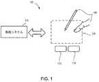
[0016]図1は、本発明の実施形態による例示的な入力装置100のブロック図である。入力装置100は、電子システム(図示せず)に入力を提供するように構成されうる。この文書で使用されるとき、用語「電子システム」(又は「電子装置」)は、広義には、情報を電子的に処理できる任意のシステムを指す。電子システムの幾つかの非限定的な例には、デスクトップコンピュータ、ラップトップコンピュータ、ネットブックコンピュータ、タブレット、ウェブブラウザ、電子書籍リーダ及び携帯情報端末(PDA)など、全てのサイズ及び形状のパーソナルコンピュータが含まれる。追加の例示的な電子システムには、入力装置100と別個のジョイスティック又はキースイッチを含む物理キーボードなどの複合入力装置が含まれる。更に他の例示的な電子システムには、データ入力装置(リモートコントロールとマウスを含む)などの周辺装置と、データ出力装置(表示画面とプリンタを含む)が含まれる。他の例には、遠隔端末、キオスク、及びテレビゲーム機(例えば、ビデオゲーム機、携帯ゲーム機など)が含まれる。他の例には、通信装置(スマートフォンなどの携帯電話を含む)と媒体装置(レコーダ、エディタ、及びテレビ、セットトップボックス、音楽プレーヤ、デジタルフォトフレーム及びデジタルカメラなどのプレーヤを含む)が含まれる。更に、電子システムは、入力装置に対してホスト又はスレーブでよい。 [0016] FIG. 1 is a block diagram of an
[0017]入力装置100は、電子システムの物理部分として実現されてもよく、電子システムから物理的に別個でもよい。必要に応じて、入力装置100は、バス、ネットワーク、及び他の有線又は無線相互接続のうちの任意の1つ以上を使用して、電子システムの部分と通信できる。例には、I2C、SPI、PS/2、ユニバーサルシリアルバス(USB)、Bluetooth、RF及びIRDAが含まれる。The
[0018]図1では、入力装置100は、検出領域120内の1つ以上の入力オブジェクト140によって提供される入力を検出するように構成された近接センサ装置(「タッチパッド」又は「タッチセンサ装置」と呼ばれることも多い)として示される。例示的な入力オブジェクトには、図1に示されるような指とスタイラスが含まれる。 [0018] In FIG. 1, the
[0019]検出領域120は、入力装置100の上、まわり、中及び/又は近くの任意の空間を包含し、入力装置100は、ユーザ入力(例えば、1つ以上の入力オブジェクト140によって提供されるユーザ入力)を検出できる。特定検出領域のサイズ、形状及び位置は、実施形態によって大きく異なりうる。幾つかの実施形態では、検出領域120は、入力装置100の表面から空間内に1つ以上の方向に、信号対雑音比によって十分に正確なオブジェクト検出が妨げられるまで延在する。この検出領域120が特定方向に延在する距離は、様々な実施形態では、約1ミリメートル未満、数ミリメートル、数センチメートル、又はそれ以上でよく、使用される検出技術のタイプと必要な精度により大きく異なりうる。したがって、幾つかの実施形態は、入力装置100の表面との接触を含まない入力、入力装置100の入力面(例えば、タッチ面)との接触を含む入力、加えられた力又は圧力のある程度の量と結合された入力装置100の入力面との接触を含む入力、及び/又はこれらの組み合わせを含む入力を検出する。様々な実施形態では、入力面は、センサ電極が中に存在するケーシングの表面、センサ電極やケーシングなどの上に被せられた表面板などによって提供されうる。幾つかの実施形態では、検出領域120は、入力装置100の入力面に投影されたときに矩形形状を有する。 [0019] The
[0020]入力装置100は、センサ構成要素と検出技術の任意の組み合わせを利用して検出領域120内のユーザ入力を検出できる。入力装置100は、ユーザ入力を検出するための1つ以上の検出要素を含む。幾つかの非限定的な例として、入力装置100は、容量、弾性、抵抗、誘導、磁気、音響、超音波及び/又は光学技術を使用できる。 The
[0021]幾つかの実施態様は、一次元、二次元、三次元又はより高次元の空間に及ぶ画像を提供するように構成される。幾つかの実施態様は、特定の軸又は平面に沿った入力の投影を提供するように構成される。 [0021] Some embodiments are configured to provide images that span one-dimensional, two-dimensional, three-dimensional or higher-dimensional spaces. Some embodiments are configured to provide a projection of the input along a particular axis or plane.
[0022]入力装置100の幾つかのキャパシタンス式の実施形態では、電圧又は電流が印加されて電界が作成される。近くの入力オブジェクトが、電界の変化を引き起こし、電圧や電流などの変化として検出されうる検出可能なキャパシタンス結合の変化を生成する。 [0022] In some capacitive embodiments of the
[0023]幾つかのキャパシタンス式の実施形態は、配列又は他の規則若しくは不規則パターンのキャパシタンス検出要素を利用して電界を作り出す。幾つかのキャパシタンス式の実施形態では、個別の検出要素をオーム的に短絡してより大きいセンサ電極を構成できる。幾つかのキャパシタンス式の実施形態は、均一な抵抗を有しうる抵抗シートを利用する。 [0023] Some capacitance-type embodiments utilize arrays or other regular or irregular pattern capacitance detection elements to create an electric field. In some capacitive embodiments, the individual sensing elements can be ohmwise shorted to form larger sensor electrodes. Some capacitance-type embodiments utilize resistance sheets that can have uniform resistance.
[0024]幾つかのキャパシタンス式の実施形態は、センサ電極と入力オブジェクトの間のキャパシタンス結合の変化に基づく「自己容量」(又は、「絶対キャパシタンス」)検出方法を利用する。様々な実施形態では、センサ電極近くの入力オブジェクトは、センサ電極近くの電界を変化させ、したがって、測定されるキャパシタンス結合が変化する。一実施態様では、絶対キャパシタンス検出方法は、センサ電極を基準電圧(例えば、系統接地)に対して変調させ、センサ電極と入力オブジェクトの間のキャパシタンス結合を検出することによって機能する。 [0024] Some capacitance-type embodiments utilize "self-capacitance" (or "absolute capacitance") detection methods based on changes in the capacitance coupling between the sensor electrode and the input object. In various embodiments, the input object near the sensor electrode changes the electric field near the sensor electrode, thus changing the measured capacitance coupling. In one embodiment, the absolute capacitance detection method works by modulating the sensor electrode to a reference voltage (eg, system ground) and detecting the capacitance coupling between the sensor electrode and the input object.
[0025]幾つかのキャパシタンス式の実施形態は、センサ電極間のキャパシタンス結合の変化に基づく「相互キャパシタンス」(又は「トランスキャパシタンス(transcapacitance)」)検出方法を利用する。様々な実施形態では、センサ電極近くの入力オブジェクトが、センサ電極間の電界を変化させ、それにより測定されたキャパシタンス結合が変化する。一実施態様では、トランスキャパシタンス検出方法は、1つ以上のトランスミッタセンサ電極(「トランスミッタ電極」又は「トランスミッタ」とも呼ばれる)と1つ以上のレシーバセンサ電極(「レシーバ電極」又は「レシーバ」とも呼ばれる)間のキャパシタンス結合を検出することによって機能する。トランスミッタセンサ電極は、基準電圧(例えば、系統接地)に対して変調されてトランスミッタ信号が送信される。レシーバセンサ電極は、派生信号の受け取りを容易にするために基準電圧に対して実質的に一定に保持されうる。派生信号は、1つ以上のトランスミッタ信号、及び/又は1つ以上の環境的干渉源(例えば、他の電磁気信号)に対応する作用を含みうる。センサ電極は、専用のトランスミッタ又はレシーバでもよく、送信と受信の両方を行うように構成されてもよい。 [0025] Some capacitance-type embodiments utilize a "mutual capacitance" (or "transcapacitance") detection method based on changes in capacitance coupling between sensor electrodes. In various embodiments, the input object near the sensor electrodes changes the electric field between the sensor electrodes, thereby changing the measured capacitance coupling. In one embodiment, the transcapacitance detection method comprises one or more transmitter sensor electrodes (also referred to as "transmitter electrodes" or "transmitters") and one or more receiver sensor electrodes (also referred to as "receiver electrodes" or "receivers"). It works by detecting the capacitance coupling between them. The transmitter sensor electrode is modulated with respect to a reference voltage (eg, system ground) to transmit the transmitter signal. The receiver sensor electrode can be kept substantially constant with respect to the reference voltage to facilitate the reception of the derived signal. Derived signals may include actions corresponding to one or more transmitter signals and / or one or more environmental interference sources (eg, other electromagnetic signals). The sensor electrodes may be dedicated transmitters or receivers and may be configured to perform both transmission and reception.
[0026]図1で、処理システム110は、入力装置100の一部として示される。処理システム110は、入力装置100のハードウェアを動作させて検出領域120内の入力を検出するように構成される。処理システム110は、1つ以上の集積回路(IC)及び/又は他の回路構成要素の一部又は全てを含む。例えば、相互キャパシタンスセンサ装置のための処理システムは、トランスミッタセンサ電極によって信号を送るように構成されたトランスミッタ回路、及び/又はレシーバセンサ電極によって信号を受け取るように構成されたレシーバ回路を含みうる。幾つかの実施形態では、処理システム110は、ファームウェアコード、ソフトウェアコードなどの電子的に読み取り可能な命令を含む。幾つかの実施形態では、入力装置100の近接検出要素など、処理システム110を構成する構成要素が一緒に配置される。他の実施形態では、処理システム110の構成要素は、入力装置100の検出要素の近くにある1つ以上の構成要素、及び他の場所にある1つ以上の構成要素と物理的に別個である。例えば、入力装置100は、デスクトップコンピュータに結合された周辺装置でもよく、処理システム110は、デスクトップコンピュータの中央処理装置及び中央処理装置とは別個の1つ以上のIC(多くの場合、関連ファームウェアを有する)上で動作するように構成されたソフトウェアを含みうる。別の例として、入力装置100は、電話に物理的に組み込まれてもよく、処理システム110は、電話の主処理装置の一部である回路とファームウェアを含みうる。幾つかの実施形態では、処理システム110は、入力装置100の実現に専用化される。他の実施形態では、処理システム110は、表示画面の動作や触覚アクチュエータの駆動などの他の機能を実行する。 [0026] In FIG. 1, the
[0027]処理システム110は、処理システム110の様々な機能を処理する1組のモジュールとして実現されうる。各モジュールは、処理システム110の一部である回路、ファームウェア、ソフトウェア又はこれらの組み合わせを含みうる。様々な実施形態では、モジュールの様々な組み合わせが使用されうる。例示的なモジュールには、センサ電極や表示画面などのハードウェアを操作するためのハードウェア操作モジュール、センサ信号や位置情報などのデータを処理するためのデータ処理モジュール、及び情報を報告するための報告モジュールが含まれる。更に他の例示的なモジュールには、入力を検出する検出要素を操作するように構成されたセンサ操作モジュール、モード変更ジェスチャなどのジェスチャを識別するように構成された識別モジュール、及び動作モードを変更するためのモード変更モジュールが含まれる。 [0027] The
[0028]幾つかの実施形態では、処理システム110は、1つ以上のアクションを行うことによって、検出領域120内のユーザ入力(又は、ユーザ入力がないこと)に直接応答する。例示的なアクションには、動作モードの変更、並びにカーソル移動、選択、メニューナビゲーション及び他の機能などのGUIアクションが含まれる。幾つかの実施形態では、処理システム110は、入力(又は、入力がないこと)に関する情報を電子システムのある部分に(例えば、別個の中央処理システムが存在する場合は、処理システム110とは別個の電子システムの中央処理システムに)提供する。幾つかの実施形態では、電子システムのある部分は、処理システム110から受け取った情報を処理して、ユーザ入力に対応し、例えば、モード変更アクションとGUIアクションを含むあらゆる種類のアクションを容易にする。 [0028] In some embodiments, the
[0029]例えば、幾つかの実施形態では、処理システム110は、入力装置100の検出要素を操作して、検出領域120内の入力(又は、入力がないこと)を示す電気信号を生成する。処理システム110は、電子システムに提供される情報を生成する際に、電気信号に適切な量の処理を実行できる。例えば、処理システム110は、センサ電極から得られたアナログ電気信号をデジタル化できる。別の例として、処理システム110は、フィルタリング又は他の信号調整を実行できる。更に別の例として、処理システム110は、情報が電気信号とベースラインとの差を反映するように、ベースラインを除去するか他の形で考慮できる。更に他の例では、処理システム110は、例えば、位置情報を決定し、入力を命令と認識し、手書きを認識できる。 [0029] For example, in some embodiments, the
[0030]「位置情報」は、ここで使用されるとき、絶対位置、相対位置、速度、加速度及び他のタイプの空間情報を広義に包含する。例示的な「ゼロ次元」位置情報には、近/遠又は接触/非接触情報が含まれる。例示的な「一次元」位置情報には、軸に沿った位置が含まれる。例示的な「二次元」位置情報には、平面内の動きが含まれる。例示的な「三次元」位置情報には、空間内の瞬間又は平均速度が含まれる。更に他の例には、空間情報の他の表現が含まれる。また、例えば、ある期間にわたって位置、動き又は瞬間速度を追跡する履歴データを含む一種類以上の位置情報に関する履歴データが、決定及び/又は記憶されうる。 [0030] "Position information" as used herein broadly includes absolute position, relative position, velocity, acceleration and other types of spatial information. Exemplary "zero-dimensional" location information includes near / far or contact / non-contact information. Illustrative "one-dimensional" position information includes position along an axis. Illustrative "two-dimensional" position information includes movement in a plane. Exemplary "three-dimensional" location information includes instantaneous or average velocities in space. Still other examples include other representations of spatial information. Also, for example, historical data about one or more types of location information, including historical data that tracks position, movement, or instantaneous velocity over a period of time, may be determined and / or stored.
[0031]幾つかの実施形態では、入力装置100は、処理システム110又は何らかの他の処理システムによって操作される付加的な入力構成要素によって実現される。そのような付加的な入力構成要素は、検出領域120内に入力するための冗長機能又は何らかの他の機能を提供できる。図1は、検出領域120の近くにあって、入力装置100を使用してアイテムの選択を容易にするために使用できるボタン130を示す。他の種類の付加的な入力構成要素には、スライダ、ボール、ホイール、スイッチなどが含まれる。これと反対に、幾つかの実施形態では、入力装置100は、他の入力構成要素なしに実現されうる。 [0031] In some embodiments, the
[0032]幾つかの実施形態では、入力装置100は、タッチスクリーンインタフェースを備え、検出領域120は、表示画面のアクティブ領域の少なくとも一部分と重なる。例えば、入力装置100は、表示画面を覆う実質的に透明なセンサ電極を備え、関連電子システムのためのタッチスクリーンインタフェースを提供できる。表示画面は、ユーザに視覚インタフェースを表示できる任意のタイプの動的表示装置でよく、かつ任意のタイプの発光ダイオード(LED)、有機LED(OLED)、陰極線管(CRT)、液晶ディスプレイ(LCD)、プラズマ、エレクトロルミネセンス(EL)又は他の表示技術を含みうる。入力装置100と表示画面は、物理要素を共用できる。例えば、幾つかの実施形態は、表示と検出に同じ電気構成要素の幾つかを利用できる。別の例として、表示画面は、処理システム110によって一部分が操作されてもよく全体が操作されてもよい。 [0032] In some embodiments, the
[0033]本発明の多くの実施形態が、完全に機能する装置の文脈で記述されるが、本発明の機構は、様々な形態のプログラム製品(例えば、ソフトウェア)として分散可能であることを理解されたい。例えば、本発明の機構は、電子処理装置によって読み取り可能な情報支持媒体(例えば、処理システム110によって読取り可能な非一時的コンピュータ読み取り可能及び/又は記録可能/書き込み可能な情報支持媒体)上にソフトウェアプログラムとして実装及び分散されうる。更に、本発明の実施形態は、分散を行うために使用される媒体の特定のタイプに関係なく等しく適用される。非一時的電子的読取り可能媒体の例には、様々なディスク、メモリスティック、メモリカード、メモリモジュールなどが含まれる。電子的読取り可能媒体は、フラッシュ、光学、磁気、ホログラフィ、又は任意の他の記憶技術に基づきうる。 Although many embodiments of the invention are described in the context of fully functional devices, it is understood that the mechanisms of the invention are distributable as various forms of program products (eg, software). I want to be. For example, the mechanisms of the invention are software on an information support medium readable by an electronic processor (eg, a non-temporary computer readable and / or recordable / writable information support medium readable by the processing system 110). It can be implemented and distributed as a program. Moreover, embodiments of the present invention apply equally regardless of the particular type of medium used to make the dispersion. Examples of non-temporary electronically readable media include various disks, memory sticks, memory cards, memory modules, and the like. The electronically readable medium can be based on flash, optical, magnetic, holographic, or any other storage technique.
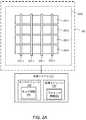
[0034]図2Aは、幾つかの実施形態による例示的パターンの検出要素の一部を示す。実例と記述を分かりやすくするために、図2Aは、検出要素を単純な長方形パターンで示し、検出要素と処理システム110の間の様々な相互接続などの様々な構成要素を示していない。電極パターン250Aは、第1の複数のセンサ電極260(260−1,260−2,260−3,...260−n)と、第1の複数の電極260の上に配置された第2の複数のセンサ電極270(270−1,270−2,270−3,...270−m)とを含む。示された例では、n=m=4であるが、一般にnとmはそれぞれ正整数であり、必ずしも互いに等しくない。様々な実施形態では、第1の複数のセンサ電極260は、複数のトランスミッタ電極(具体的には「トランスミッタ電極260」と呼ばれる)として作動され、第2の複数のセンサ電極270は、複数のレシーバ電極(具体的には「レシーバ電極270」と呼ばれる)として作動される。別の実施形態では、ある複数のセンサ電極が、送受信するように構成され、他の複数のセンサ電極が、送受信するように構成されうる。更に他の処理システム110は、派生信号を第1及び/又は第2の複数のセンサ電極の1つ以上のセンサ電極によって受け取り、1つ以上のセンサ電極が、絶対キャパシタンス検出信号によって変調される。第1の複数のセンサ電極260、第2の複数のセンサ電極270又はこれらの両方は、検出領域120内に配置されうる。電極パターン250Aは、処理システム110に結合されうる。 [0034] FIG. 2A shows some of the detection elements of an exemplary pattern according to some embodiments. For clarity of illustration and description, FIG. 2A shows the detection elements in a simple rectangular pattern and does not show various components such as various interconnections between the detection element and the
[0035]第1の複数の電極260と第2の複数の電極270は、典型的には、互いにオーム的に分離される。即ち、1つ以上の絶縁体が、第1の複数の電極260と第2の複数の電極270を分離し、それらの電極が互いに電気的に短絡するのを防ぐ。幾つかの実施形態では、第1の複数の電極260と第2の複数の電極270は、交差領域で間に配置された絶縁材料によって分離され、そのような構造では、第1の複数の電極260及び/又は第2の複数の電極270が、同じ電極の異なる部分を接続するジャンパによって構成されうる。幾つかの実施形態では、第1の複数の電極260と第2の複数の電極270が、1つ以上の絶縁材料層によって分離される。そのような実施形態では、第1の複数の電極260と第2の複数の電極270が、共通基板の別個の層上に配置されうる。他の幾つかの実施形態では、第1の複数の電極260と第2の複数の電極270が、1つ以上の基板によって分離され、例えば、第1の複数の電極260と第2の複数の電極270が、同じ基板の両側に配置されてもよく、積層された異なる基板上に配置されてもよい。幾つかの実施形態では、第1の複数の電極260と第2の複数の電極270が、単一基板の同じ側に配置されうる。 [0035] The first plurality of electrodes 260 and the second plurality of electrodes 270 are typically ohmically separated from each other. That is, one or more insulators separate the first plurality of electrodes 260 and the second plurality of electrodes 270 to prevent the electrodes from being electrically short-circuited with each other. In some embodiments, the first plurality of electrodes 260 and the second plurality of electrodes 270 are separated by an insulating material disposed between the intersecting regions, and in such a structure, the first plurality of electrodes. 260 and / or a second plurality of electrodes 270 may be configured by jumpers connecting different parts of the same electrode. In some embodiments, the first plurality of electrodes 260 and the second plurality of electrodes 270 are separated by one or more insulating material layers. In such an embodiment, the first plurality of electrodes 260 and the second plurality of electrodes 270 may be arranged on separate layers of a common substrate. In some other embodiments, the first plurality of electrodes 260 and the second plurality of electrodes 270 are separated by one or more substrates, for example, the first plurality of electrodes 260 and the second plurality of electrodes. The electrodes 270 may be arranged on both sides of the same substrate, or may be arranged on different laminated substrates. In some embodiments, the first plurality of electrodes 260 and the second plurality of electrodes 270 may be located on the same side of a single substrate.
[0036]第1の複数のセンサ電極260と第2の複数センサ電極270の間の局所的なキャパシタンス結合領域が、「キャパシタンス画像」の「キャパシタンス画素」を構成する。第1と第2の複数のセンサ電極260と270間のキャパシタンス結合は、検出領域120内の入力オブジェクトの近さと動きにより変化する。更に、様々な実施形態では、第1の複数のセンサ電極260と第2の複数のセンサ電極270のそれぞれと入力オブジェクトとの間の局所的なキャパシタンス結合は、「キャパシタンス画像」の「キャパシタンス画素」と呼ばれうる。幾つかの実施形態では、第1の複数のセンサ電極260と第2の複数のセンサ電極270のそれぞれと入力オブジェクトとの間の局所的なキャパシタンス結合は、「キャパシタンスプロファイル」の「キャパシタンス測定値」と呼ばれうる。 [0036] The local capacitance coupling region between the first plurality of sensor electrodes 260 and the second plurality of sensor electrodes 270 constitutes the "capacitance pixel" of the "capacitance image". The capacitance coupling between the first and second plurality of sensor electrodes 260 and 270 changes depending on the proximity and movement of the input object in the
[0037]処理システム110は、センサ回路204を有するセンサモジュール208を含みうる。センサモジュール208は、電極パターン250Aを作動させて、検出周波数を有するキャパシタンス検出信号を使用する電極パターンの電極から派生信号を受け取る。処理システム110は、派生信号からキャパシタンス測定値を決定するように構成された処理モジュール220を含みうる。処理モジュール220は、デジタル信号プロセッサ(DSP)、マイクロプロセッサなどのプロセッサ回路222を含みうる。処理モジュール220は、本明細書に記載された機能を実施するためにプロセッサ回路222によって実行するように構成されたソフトウェア及び/又はファームウェアを含みうる。あるいは、プロセッサモジュール220の機能の幾つか又は全ては、ハードウェアで完全に実現されうる(例えば、集積回路を使用して)。処理モジュール220は、キャパシタンス測定値の変化を追跡して検出領域120の入力オブジェクトを検出できる。処理システム110は、他のモジュール構成を含むことができ、また、センサモジュール208と処理モジュール220によって実行される機能は、一般に、処理システム110内の1つ以上のモジュール又は回路によって実行されうる。処理システム110は、他のモジュール及び回路を含むことができ、以下の幾つかの実施形態で記述されるような他の機能を実行できる。 The
[0038]処理システム110は、絶対キャパシタンス検出モード又はトランスキャパシタンス検出モードで動作できる。絶対キャパシタンス検出モードでは、センサ回路204内のレシーバが、電極パターン250Aのセンサ電極上の電圧、電流又は電荷を測定し、センサ電極が、絶対キャパシタンス検出信号で変調されて派生信号を生成する。処理モジュール220は、派生信号から絶対キャパシタンス測定値を生成する。処理モジュール220は、絶対キャパシタンス測定値の変化を追跡して検出領域120内の入力オブジェクトを検出できる。 [0038] The
[0039]トランスキャパシタンス検出モードでは、センサ回路204内のトランスミッタが、第1の複数の電極260の1つ以上を、キャパシタンス検出信号(トランスキャパシタンス検出モードではトランスミッタ信号又は変調信号とも呼ばれる)によって駆動する。センサ回路204内のレシーバは、第2の複数の電極270の1つ以上における電圧、電流及び電荷を測定して派生信号を生成する。派生信号は、検出領域120内のキャパシタンス検出信号及び入力オブジェクトの影響を含む。処理モジュール220は、派生信号からトランスキャパシタンス測定値を生成する。処理モジュール220は、トランスキャパシタンス測定値の変化を追跡して検出領域120内の入力オブジェクトを検出できる。 [0039] In the trans-capacitance detection mode, the transmitter in the
[0040]幾つかの実施形態では、処理システム110は、電極パターン250Aを「走査」してキャパシタンス測定値を決定する。トランスキャパシタンス検出モードでは、処理システム110は、第1の複数の電極260を駆動してトランスミッタ信号を送信する。処理システム110は、1つのトランスミッタ電極が一度に送信するか複数のトランスミッタ電極が同時に送信するように、第1の複数の電極260を作動できる。複数のトランスミッタ電極が同時に送信する場合、それらの複数のトランスミッタ電極が、同じトランスミッタ信号を送信し、より大きいトランスミッタ電極を有効に生成してもよく、それらの複数のトランスミッタ電極が、異なるトランスミッタ信号を送信してもよい。例えば、複数のトランスミッタ電極は、様々なトランスミッタ信号を、第2の複数の電極270の派生信号に対する複合効果を独立に決定可能にする1つ以上のコード体系に従って、送信できる。絶対キャパシタンス検出モードでは、処理システム110は、派生信号を、1つのセンサ電極260,270から一度に受け取ってもよく、複数のセンサ電極260,270から一度に受け取ってもよい。いずれのモードでも、処理システム110は、第2の複数の電極270を単独又は一緒に作動させて派生信号を取得できる。絶対キャパシタンス検出モードでは、処理システム110は、1つ以上の軸に沿った全ての電極を同時に駆動できる。幾つかの例では、処理システム110は、1つの軸に沿った(例えば、第1の複数のセンサ電極260に沿った)電極を駆動でき、同時に別の軸に沿った電極が、シールド信号やガード信号などによって駆動される。幾つかの例では、1つの軸に沿った幾つかの電極と他の軸に沿った幾つかの電極が、同時に駆動されうる。 [0040] In some embodiments, the
[0041]トランスキャパシタンス検出モードでは、処理システム110は、派生信号を使用してキャパシタンス画素におけるキャパシタンス測定値を決定できる。キャパシタンス画素からの1組の測定値が、画素におけるキャパシタンス測定値を表す「キャパシタンス画像」(「キャパシタンスフレーム」とも呼ばれる)を構成する。処理システム110は、複数の時間期間にわたる複数のキャパシタンス画像を取得でき、キャパシタンス画像の間の差を決定して検出領域120内の入力に関する情報を取得できる。例えば、処理システム110は、連続時間期間にわたって取得された連続キャパシタンス画像を使用して、検出領域120に入る、出る、及びその中の1つ以上の入力オブジェクトの動きを追跡できる。 [0041] In transcapacitance detection mode, the
[0042]絶対キャパシタンス検出モードで、処理システム110は、派生信号を使用して、センサ電極260の軸及び/又はセンサ電極270の軸に沿ったキャパシタンス測定値を決定できる。1組のそのような測定値が、軸に沿ったキャパシタンス測定値を表す「キャパシタンスプロファイル」を構成する。処理システム110は、複数の時間期間にわたって軸の一方又は両方に沿った複数のキャパシタンスプロファイルを得ることができ、キャパシタンスプロファイル間の差を決定して検出領域120内の入力に関する情報を取得できる。例えば、処理システム110は、連続時間期間にわたって取得された連続キャパシタンスプロファイルを使用して、検出領域120内の入力オブジェクトの位置又は近さを追跡できる。他の実施形態では、各センサは、キャパシタンス画像のキャパシタンス画素でよく、絶対キャパシタンス検出モードを使用して、キャパシタンスプロファイルの追加又は代替としてキャパシタンス画像を生成できる。 [0042] In absolute capacitance detection mode, the
[0043]入力装置100のベースラインキャパシタンスは、検出領域120内の入力オブジェクトと関連しないキャパシタンス画像又はキャパシタンスプロファイルである。ベースラインキャパシタンスは、環境及び動作条件により変化し、処理システム110は、ベースラインキャパシタンスを様々な方法で評価できる。例えば、幾つかの実施形態では、処理システム110は、検出領域120内に入力オブジェクトがないことが決定されたときに「ベースライン画像」又は「ベースラインプロファイル」を取得し、そのベースライン画像又はベースラインプロファイルをベースラインキャパシタンスの評価として使用する。処理モジュール220は、キャパシタンス測定値におけるベースラインキャパシタンスを考慮でき、したがって、キャパシタンス測定値は、「デルタキャパシタンス測定値」と呼ばれうる。したがって、用語「キャパシタンス測定値」は、本明細書で使用されるとき、決定されたベースラインに対するデルタ測定値を含む。 [0043] The baseline capacitance of the
[0044]幾つかのタッチスクリーン実施形態では、第1の複数のセンサ電極260と第2の複数のセンサ電極270の少なくとも一方は、「Vcom」電極(コモン電極)、ゲート電極、ソース電極、アノード電極及び/又はカソード電極の1つ以上のセグメントなど、表示画面の表示の更新に使用される表示装置280の1つ以上の表示電極を備える。これらの表示電極は、適切な表示画面基板上に配置されうる。例えば、表示電極は、何らかの表示画面(例えば、インプレーンスイッチング(IPS)又はプレーントゥラインスイッチング(PLS)有機発光ダイオード(OLED))内の透明基板(ガラス基板、TFTガラス、又は他の透明材料)上、放射層(OLED)の上の何らかの表示画面のカラーフィルタガラス(例えば、パターンドバーチカルアライメント(Patterned Vertical Alignment)(PVA)又はマルチドメインバーチカルアライメント(Multi-domain Vertical Alignment)(MVA))の底面上などに配置されうる。表示電極は、表示更新及びキャパシタンス検出の機能を実行するので、「組み合わせ電極」とも呼ばれうる。様々な実施形態では、第1及び第2の複数のセンサ電極260及び270の各センサ電極は、1つ以上の組み合わせ電極を含む。他の実施形態では、第1の複数のセンサ電極260の少なくとも2つのセンサ電極、又は第2の複数のセンサ電極270の少なくとも2つのセンサ電極が、少なくとも1つの組み合わせ電極を共用できる。更に、一実施形態では、第1の複数のセンサ電極260と第2の複数電極270の両方が、表示画面基板上の表示スタック内に配置される。更に、表示スタック内のセンサ電極260,270の少なくとも1つが、組み合わせ電極を含みうる。しかしながら、他の実施形態では、第1の複数のセンサ電極260又は第2の複数のセンサ電極270だけ(両方ではなく)が、表示スタック内に配置され、一方、他のセンサ電極は、表示スタックの外側にある(例えば、カラーフィルタガラスの反対側に配置される)。 [0044] In some touch screen embodiments, at least one of the first plurality of sensor electrodes 260 and the second plurality of sensor electrodes 270 is a "Vcom" electrode (common electrode), a gate electrode, a source electrode, an anode. It comprises one or more display electrodes of the
[0045]一実施形態では、処理システム110は、センサモジュール208、処理モジュール220及び任意の他のモジュール及び/又は回路を有する、特定用途向け集積回路(ASIC)などの単一の一体型コントローラを備える。別の実施形態では、処理システム110は、複数の集積回路を含むことができ、センサモジュール208、処理モジュール220、及び任意の他のモジュール及び/又は回路が集積回路間に分割されうる。例えば、センサモジュール208が、1つの集積回路上にあってもよく、処理モジュール220及び任意の他のモジュール及び/回路が、1つ以上の他の集積回路でよい。幾つかの実施形態では、センサモジュール208の第1の部分が、1つの集積回路上にあってもよく、センサモジュール208の第2の部分が、第2の集積回路上にあってもよい。そのような実施形態では、第1と第2の集積回路の少なくとも一方が、ドライバモジュール及び/又は表示ドライバモジュールなどの他のモジュールの少なくとも一部分を含む。 [0045] In one embodiment, the
[0046]図2Bは、幾つかの実施形態による検出要素の別の例示的パターンの一部分を示す。例証と記述を分かりやすくするために、図2Bは、検出要素を矩形マトリクスで示し、処理システム110と検出要素の間の様々な相互接続などの様々な構成要素を示していない。電極パターン250Bは、矩形マトリクスに配置された複数のセンサ電極210を含む。電極パターン250Bは、J行K列で配列されたセンサ電極210J,K(集合的にセンサ電極210と呼ばれる)を含み、ここで、JとKは正整数であるが、1又はJ及びKはゼロであってもよい。電極パターン250Bが、極配列(polar array)、繰り返しパターン、非繰り返しパターン、不均一配列、単一行又は列、又は他の適切な配列など、センサ電極210の他のパターンを含みうる。更に、センサ電極210は、円形、矩形、菱形、星形、四角形、非凸状、凸状、非凹状、凹状などの任意の形状でよい。更に、センサ電極210は、複数の別個のサブ電極に細分されうる。電極パターン250は、処理システム110に結合される。[0046] FIG. 2B shows a portion of another exemplary pattern of detection elements according to some embodiments. For clarity of illustration and description, FIG. 2B shows the detection elements in a rectangular matrix and does not show various components such as various interconnections between the
[0047]センサ電極210は、典型的には、互いにオーム的に分離される。更に、センサ電極210が複数のサブ電極を含む場合、サブ電極は、互いにオーム的に分離されうる。更に、一実施形態では、センサ電極210は、センサ電極210の間にあるグリッド電極218からオーム的に分離されうる。一例では、グリッド電極218は、グリッド電極218の窓216内に配置されたセンサ電極210の1つ以上を取り囲みうる。幾つかの実施形態では、電極パターン250Bは、複数のグリッド電極218を含みうる。幾つかの実施形態では、グリッド電極218は、1つ以上のセグメントを含みうる。グリッド電極218は、シールドとして使用されるか、センサ電極210によるキャパシタンス検出を行なうときに使用するガード信号を伝えるために使用されうる。代替又は追加として、グリッド電極218は、キャパシタンス検出を行なうときのセンサ電極として使用されうる。更に、グリッド電極218は、センサ電極210と同一平面でよいが、これは要件ではない。例えば、グリッド電極218は、異なる基板上、又はセンサ電極210と同じ基板の異なる側に配置されうる。グリッド電極218は必須ではなく、幾つかの実施形態では、グリッド電極218は存在しない。 [0047] The
[0048]第1の動作モードで、処理システム110は、少なくとも1つのセンサ電極210を使用して、絶対キャパシタンス検出により入力オブジェクトの存在を検出できる。センサモジュール208は、センサ電極210上の電圧、電荷又は電流を測定して、センサ電極210と入力オブジェクト間のキャパシタンスを示す派生信号を取得できる。処理モジュール220は、派生信号を使用して絶対キャパシタンス測定値を決定する。電極パターン250Bのとき、絶対キャパシタンス測定値を使用してキャパシタンス画像を形成できる。 [0048] In the first mode of operation, the
[0049]第2の動作モードで、処理システム110は、センサ電極210群を使用して、トランスキャパシタンス検出によって入力オブジェクトの存在を検出できる。センサモジュール208は、センサ電極210の少なくとも1つのセンサ電極をトランスミッタ信号によって駆動でき、またセンサ電極210の少なくとも1つの他のセンサ電極から派生信号を受け取りうる。処理モジュール220は、派生信号を使用してトランスキャパシタンス測定値を決定しかつキャパシタンス画像を形成する。 [0049] In the second mode of operation, the
[0050]入力装置100は、前述したモードのいずれでも動作するように構成されうる。また、入力装置100は、前述したモードのいずれか2つ以上のモード間で切り替わるように構成されうる。処理システム110は、図2Aに関して前述したように構成されうる。 [0050] The
[0051]幾つかの実施形態では、処理システム110は、更に、入力オブジェクトのフォース情報を決定するように構成される。処理システム110は、表示装置に組み込まれたセンサ電極から得られた絶対キャパシタンス測定値に応じたフォース情報を決定できる。更に後述するように、入力装置100の表示装置は、入力オブジェクトによって加えられる力に応じて湾曲できる。表示装置が湾曲する結果、表示装置に組み込まれたセンサ電極の少なくとも一部分が平衡状態から撓む。加えられた力によってセンサ電極が撓む結果、絶対キャパシタンス測定値が変化する。フォース情報は、センサ電極の構成により、「フォース画像」、「フォースプロファイル」又はスカラフォース値を含みうる。例えば、センサ電極パターン250Bから得られた絶対キャパシタンス測定値を使用して、フォース画像又はフォーススカラ値を生成できる。別の例では、センサ電極パターン250Aから得られた絶対キャパシタンス測定値を使用して、フォースプロファイル又はフォーススカラ値を生成できる。いずれの場合も、フォース情報を位置情報と組み合わせて、入力オブジェクトの位置と、入力オブジェクトによって加えられる力の両方を決定できる。別の実施形態では、力の大きさを測定してスカラフォース値を決定できる。スカラフォース値を位置情報と組み合わせてフォース画像又はフォースプロファイルを生成できる。 [0051] In some embodiments, the
[0052]図3は、一実施形態による入力装置100の断面を示すブロック図である。入力装置100は、入力面301、表示セル314A、バックライト308、空隙/圧縮性層310、及び少なくとも1つの導電性電極(導電性電極312)を備える。入力面301は、ガラス基板などの透明基板を含みうる。導電性電極312は、金属電極でよい。一実施形態では、導電性電極312は、単一の導電性バックプレーンを含む。別の実施形態では、導電性バックプレーンを部分に細分でき、導電性電極312は、導電性バックプレーンの一部分を含みうる。導電性電極312は、電気接地又は系統接地などの基準電圧に電気的に結合されうる。 [0052] FIG. 3 is a block diagram showing a cross section of the
[0053]一実施形態では、表示セル314Aは、カラーフィルタ基板302、内部層305、及び薄膜トランジスタ(TFT)基板306を含む。内部層305は、カラーフィルタ層、液晶ディスプレイ(LCD)材料層、導電体層、絶縁体層などの様々な層を含みうる。詳細には、内部層305は、センサ電極304を構成する1つ以上の導電体層を含む。カラーフィルタ基板302、内部層305及びTFT基板306は柔軟であり、その結果、表示セル314Aが柔軟になる。 [0053] In one embodiment, the
[0054]センサ電極304は、様々な構成を有しうる。一例では、センサ電極304は、センサ電極パターン250Aの複数のセンサ電極260を含みうる。一例では、センサ電極304は、センサ電極パターン250Aの複数のセンサ電極260と複数のセンサ電極270を含みうる。別の例では、センサ電極304は、センサ電極パターン250Bのセンサ電極210を含みうる。任意の構成で、センサ電極304はそれぞれ、表示更新及びキャパシタンス検出のために構成された少なくとも1つのコモン電極を備える。 [0054] The sensor electrode 304 may have various configurations. In one example, the sensor electrode 304 may include a plurality of sensor electrodes 260 of the sensor electrode pattern 250A. In one example, the sensor electrode 304 may include a plurality of sensor electrodes 260 and a plurality of sensor electrodes 270 of the sensor electrode pattern 250A. In another example, the sensor electrode 304 may include the
[0055]表示セル314Aは、入力面301とバックライト308の間に配置される。表示セル314Aは、柔軟であり、力が入力面301に加えられたときに屈曲又は湾曲できる。この例では、導電性電極312は、空隙又は圧縮性層310でよい空隙/圧縮性層310によってバックライト308から分離される。従って、センサ電極304は、入力面301と導電性電極312の間に配置される。センサ電極304は、入力面301に加えられた力に応じて表示セル314が空隙/圧縮性層310内に湾曲するときに導電性電極312の方に撓むように構成される。入力面301に加えられる力の位置によって、センサ電極304の少なくとも一部分が、印加力に応じて導電性電極312の方に撓む。 [0055] The
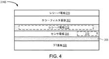
[0056]図4は、一実施形態による別の表示セル314Bの断面を示すブロック図である。一実施形態では、表示セル314Bは、表示セル314Aの代わりに使用されうる。表示セル314B内で、レシーバ電極316が、カラーフィルタ基板302上に配置される。一実施形態では、センサ電極304は、トランスミッタ電極として動作する複数のセンサ電極260を含みうる。レシーバ電極316は、センサ電極パターン250Aの複数のセンサ電極270を含みうる。別の実施形態では、レシーバ電極316は、カラーフィルタ基板316上ではなく、内部層305内に配置される。更に別の実施形態では、レシーバ電極316は、センサ電極304と同じ層上に配置される。 FIG. 4 is a block diagram showing a cross section of another
[0057]図5は、別の実施形態による入力装置100の断面を示すブロック図である。この実施形態では、導電性電極312は、表示セル314の下でかつバックライト308の上に配置される。表示セル314は、表示セル314A、表示セル314Bなどを含みうる。例えば、導電性電極312は、表示セル314のTFT基板306の下に配置されうる。導電性電極312は、空隙/圧縮性層310によって表示セル314から分離される。[0057] FIG. 5 is a block diagram showing a cross section of the
[0058]図3〜図5の実施形態で、OLEDディスプレイなどの他のタイプのフレキシブル表示セルが使用されうる。一般に、表示セルは、LED、OLED、プラズマセル、電子インク素子、LCD構成要素、又はフレキシブルディスプレイと適合する他の適切な表示画素構造から構成された表示画素を含みうる。センサ電極304は、表示セル内に配置され、フレキシブルディスプレイを曲げる力が加えられたときに導電性電極312の方に撓む。 [0058] In the embodiments of FIGS. 3-5, other types of flexible display cells, such as OLED displays, may be used. In general, display cells may include display pixels composed of LEDs, OLEDs, plasma cells, electronic ink elements, LCD components, or other suitable display pixel structures compatible with flexible displays. The sensor electrode 304 is arranged in the display cell and bends toward the
[0059]図6は、一実施形態による入力オブジェクトによって入力装置100に加えられた力を示す概略断面図である。入力オブジェクト(例えば、指)が、入力面(図6に示されず)に力を加え、その力が、表示セル314を曲げる。表示セル314内に配置されたセンサ電極305が、導電性電極312の方に撓む。図7は、図6に示された印加力が与えられた入力装置100の平面図である。図7の例では、センサ電極304は、センサ電極パターン250Bのセンサ電極210を含む。領域702内のセンサ電極210の一部分は、印加力に応じて導電性電極312の方に撓む。センサ電極パターン250Bは、例で示されているが、他のセンサ電極パターンを使用できる(例えば、センサ電極パターン250A)。一般に、入力装置100に加えられる所定の力によって、センサ電極305の少なくとも一部分が導電性電極312の方に撓む。図7の例では、導電性電極312は、単一のバックプレーンを含むが、前述のような他の構成も使用できる。一実施形態では、導電性電極312の表面積は、センサ電極305それぞれの表面積より大きい。 FIG. 6 is a schematic cross-sectional view showing the force applied to the
[0060]図8は、一実施形態による一体型表示装置及びキャパシタンス検出装置を作動させる方法800を示す流れ図である。方法800は、前述された処理システム110によって、入力装置100と相互作用する入力オブジェクトのフォース情報、又はフォース情報と位置情報両方を決定するために実行されうる。一実施形態では、処理システム110は、垂直帰線消去時間や水平帰線消去時間などの非表示更新時間中に、方法800の全て又は一部を実行する。別の実施形態では、非表示更新時間は、表示フレームの表示線更新の間に生じかつ少なくとも表示線更新期間と同じ長さの水平帰線消去期間でよい。幾つかの実施形態では、1つの非表示更新期間をフォース検出のために使用でき、他の非表示更新期間をタッチ検出のために使用できる。 [0060] FIG. 8 is a flow chart showing a
[0061]方法800は、ステップ802で始まり、処理システム110は、キャパシタンス検出のためのセンサ電極を作動させる。センサ電極パターン250A又はセンサ電極パターン250Bのための絶対キャパシタンス検出やトランスキャパシタンス検出などのキャパシタンス検出のための様々な技術については前述された。 [0061]
[0062]ステップ804で、処理システム110は、絶対キャパシタンス検出のためのセンサ電極を駆動する。絶対キャパシタンス検出の技術については前述された。センサ回路204は、絶対キャパシタンス検出のためにセンサ電極260又はセンサ電極210を駆動できる。一実施形態では、ステップ806で、処理システム110は、トランスキャパシタンス検出のためにセンサ電極を駆動できる。トランスキャパシタンス検出の技術については前述された。センサ電極パターン250Aの場合、センサ回路204は、センサ電極270から派生信号を受け取りながらセンサ電極260をトランスミッタ信号で駆動できる。センサ電極パターン250Bの場合、センサ回路204は、他のセンサ電極210から派生信号を受け取りながら幾つかのセンサ電極210をトランスミッタ信号で駆動できる。 [0062] In
[0063]ステップ808で、処理システム110は、センサ電極の少なくとも一部分の絶対キャパシタンスの変化を決定する。ステップ810で、処理システム110は、絶対キャパシタンスの変化に基づいて入力オブジェクトのフォース情報を決定する。前述したように、入力装置100に加えられる力に応じて、フレキシブルディスプレイ内のセンサ電極の一部分が、導電性電極の方に撓む。そのような撓んだ電極の絶対キャパシタンスは、その電極が導電性電極の方に撓むときに変化する。絶対キャパシタンスのこの変化を測定することによって、処理システム110は、フォース情報を決定できる。 [0063] In step 808, the
[0064]ステップ812で、処理システム110は、また、絶対キャパシタンス測定値及び/又はトランスキャパシタンス測定値に基づいて入力オブジェクトの位置情報を決定できる。処理システム110は、位置情報とフォース情報を組み合わせて、入力オブジェクトの位置と、入力オブジェクトによって入力装置100に加えられた力を決定できる。 [0064] In step 812, the
[0065]ここに述べられた実施形態及び例は、本技術とその特定の応用による実施形態を最もよく説明し、それにより当業者が本発明を作成し使用できるようにするために提示された。しかしながら、当業者は、以上の記述と例が、例証と実施例のためのみに提示されたことを理解するであろう。示された記述は、網羅的なものではなく、本発明を開示された厳密な形に限定するものでもない。 [0065] The embodiments and examples described herein have been presented to best describe embodiments of the present technology and its particular applications, thereby allowing those skilled in the art to develop and use the present invention. .. However, one of ordinary skill in the art will appreciate that the above description and examples are presented solely for illustration and examples. The statements presented are not exhaustive and do not limit the invention to the exact form disclosed.
[0066]以上を考慮して、本開示の範囲は、以下の特許請求の範囲によって決定される。 [0066] In view of the above, the scope of the present disclosure is determined by the following claims.
100 入力装置
110 処理システム
120 検出領域
130 ボタン
140 入力オブジェクト
204 センサ回路
208 センサモジュール
220 処理モジュール
222 プロセッサ回路100
Claims (16)
Translated fromJapanese複数のセンサ電極と、
前記複数のセンサ電極が設けられている層と異なる層に設けられている複数のレシーバ電極と、
前記複数のセンサ電極の下に配置された柔軟な薄膜トランジスタ(TFT)基板と、
前記TFT基板の下に配置された少なくとも1つの導電性電極と、
前記複数のセンサ電極に結合される処理システムと、を備え、
前記複数のセンサ電極のそれぞれは、表示更新及びキャパシタンス検出用に構成される少なくとも1つのコモン電極を備え、
前記複数のセンサ電極及び前記TFT基板は、前記入力面と前記少なくとも1つの導電性電極の間に配置され、
前記入力面に力が加えられたとき、前記TFT基板が湾曲して前記複数のセンサ電極が前記導電性電極の方に撓み、
前記処理システムは、
前記複数のセンサ電極の少なくとも一部分の絶対キャパシタンスの変化を検出し、
前記絶対キャパシタンスの変化に基づいて入力オブジェクトのフォース情報を決定し、
前記複数のレシーバ電極から派生信号を受信している間、前記複数のセンサ電極をトランスミッタ信号で駆動し、
前記派生信号に基づいて前記入力面近くの入力オブジェクトの位置情報を決定するように構成される、一体型表示装置及びキャパシタンス検出装置。An integrated display device and capacitance detection device having an input surface.
With multiple sensor electrodes,
A plurality of receiver electrodes provided in a layer different from the layer in which the plurality of sensor electrodes are provided, and
A flexible thin film transistor (TFT) substrate arranged under the plurality of sensor electrodes.
With at least one conductive electrode arranged under the TFT substrate,
A processing system coupled to the plurality of sensor electrodes is provided.
Each of the plurality of sensor electrodes comprises at least one common electrode configured for display update and capacitance detection.
The plurality of sensor electrodes and the TFT substrate are arranged between the input surface and the at least one conductive electrode.
When a force is applied to the input surface, the TFT substrate is curved and the plurality of sensor electrodes are bent toward the conductive electrodes.
The processing system
The change in the absolute capacitance of at least a part of the plurality of sensor electrodes is detected, and the change is detected.
Whereindetermining the force information of an input object based on a change in the absolute capacitance,
While receiving derivative signals from the plurality of receiver electrodes, the plurality of sensor electrodes are driven by the transmitter signal, and the plurality of sensor electrodes are driven by the transmitter signal.
An integrated display device and capacitance detection deviceconfigured to determine the position information of an input object near the input surface based on the derived signal.
前記少なくとも1つの導電性電極は、前記バックライトの下に配置される、請求項1に記載の装置。Further equipped with a backlight arranged under the TFT substrate,
The device according to claim 1, wherein the at least one conductive electrode is arranged under the backlight.
前記複数のセンサ電極を作動させるように構成され、前記複数のレシーバ電極に結合され、前記複数のレシーバ電極から派生信号を受信する間、前記複数のセンサ電極をトランスミッタ信号で駆動するように構成されたセンサ回路を含むセンサモジュールと、
前記センサ回路に結合される処理回路と、を備え、
前記複数のセンサ電極のそれぞれは、表示更新及びキャパシタンス検出用に構成される少なくとも1つのコモン電極を備え、
前記処理回路は、
前記複数のセンサ電極の少なくとも一部分の絶対キャパシタンスの変化を検出し、
前記絶対キャパシタンスの変化に基づいて入力オブジェクトのフォース情報を決定するように構成され、
前記派生信号に基づいて前記入力オブジェクトの位置情報を決定するように構成され、
前記複数のセンサ電極と前記TFT基板とは、前記入力面と少なくとも1つの導電性電極との間に配置され、
前記入力面に力が加えられたとき、前記TFT基板が湾曲して前記複数のセンサ電極が前記導電性電極の方に撓む、処理システム。An input surface, a plurality of sensor electrodes, aplurality of receiver electrodes provided in a layer different from the layer in which the plurality of sensor electrodes are provided, and a flexible TFT substrate arranged under the plurality of sensor electrodes. A processing system for an integrated display device and a capacitance detection device having at least one conductive electrode arranged under the TFT substrate.
It is configured to actuate the plurality of sensor electrodes, coupled to the plurality of receiver electrodes, and drive the plurality of sensor electrodes with a transmitter signal while receiving derivative signals from the plurality of receiver electrodes. a sensor module including a sensorcircuit,
A processing circuit coupled to the sensor circuit is provided.
Each of the plurality of sensor electrodes comprises at least one common electrode configured for display update and capacitance detection.
The processing circuit
The change in the absolute capacitance of at least a part of the plurality of sensor electrodes is detected, and the change is detected.
It is configured to determine the force information of the input object based on the change in absolute capacitance.
It is configured to determine the position information of the input object based on the derived signal.
The plurality of sensor electrodes and the TFT substrate are arranged between the input surface and at least one conductive electrode.
A processing system in which when a force is applied to the input surface, the TFT substrate is curved and the plurality of sensor electrodes are bent toward the conductive electrodes.
前記複数のセンサ電極を作動させ、
前記複数のセンサ電極の少なくとも一部分の絶対キャパシタンスの変化を検出し、
前記絶対キャパシタンスの変化に基づいて入力オブジェクトのフォース情報を決定し、
前記複数のレシーバ電極から派生信号を受信している間、前記複数のセンサ電極をトランスミッタ信号で駆動し、
前記派生信号に基づいて前記入力面近くの入力オブジェクトの位置情報を決定し、
前記複数のセンサ電極のそれぞれは、表示更新及び前記キャパシタンス検出用に構成される少なくとも1つのコモン電極を備え、
前記複数のセンサ電極と前記TFT基板とは、前記入力面と少なくとも1つの導電性電極の間に配置され、
前記入力面に力が加えられたとき、前記TFT基板が湾曲して前記複数のセンサ電極が前記導電性電極の方に撓む、方法。It is arranged under the input surface, a plurality of sensor electrodes for capacitance detection,a plurality of receiver electrodes provided in a layer different from the layer in which the plurality of sensor electrodes are provided, and the plurality of sensor electrodes. A method of operating an integrated display device and a capacitance detection device having a flexible TFT substrate and at least one conductive electrode arranged under the TFT substrate.
The plurality of sensor electrodes are operated to operate the plurality of sensor electrodes.
The change in the absolute capacitance of at least a part of the plurality of sensor electrodes is detected, and the change is detected.
The force information of the input object is determined based on the change in absolute capacitance.
While receiving derivative signals from the plurality of receiver electrodes, the plurality of sensor electrodes are driven by the transmitter signal, and the plurality of sensor electrodes are driven by the transmitter signal.
The position information of the input object near the input surface is determined based on the derived signal, and the position information is determined.
Each of the plurality of sensor electrodes comprises at least one common electrode configured for display update and capacitance detection.
The plurality of sensor electrodes and the TFT substrate are arranged between the input surface and at least one conductive electrode.
A method in which when a force is applied to the input surface, the TFT substrate is curved and the plurality of sensor electrodes are bent toward the conductive electrodes.
Applications Claiming Priority (5)
| Application Number | Priority Date | Filing Date | Title |
|---|---|---|---|
| US201562160554P | 2015-05-12 | 2015-05-12 | |
| US62/160,554 | 2015-05-12 | ||
| US14/871,497US9733756B2 (en) | 2015-05-12 | 2015-09-30 | Integrated display device and sensing device with force sensing |
| US14/871,497 | 2015-09-30 | ||
| PCT/US2016/028307WO2016182702A1 (en) | 2015-05-12 | 2016-04-19 | Integrated display device and sensing device with force sensing |
Publications (2)
| Publication Number | Publication Date |
|---|---|
| JP2018521383A JP2018521383A (en) | 2018-08-02 |
| JP6932646B2true JP6932646B2 (en) | 2021-09-08 |
Family
ID=57249072
Family Applications (1)
| Application Number | Title | Priority Date | Filing Date |
|---|---|---|---|
| JP2017557963AActiveJP6932646B2 (en) | 2015-05-12 | 2016-04-19 | Integrated display and detection device with force detection function |
Country Status (5)
| Country | Link |
|---|---|
| US (1) | US9733756B2 (en) |
| JP (1) | JP6932646B2 (en) |
| KR (1) | KR102312138B1 (en) |
| CN (1) | CN107533405B (en) |
| WO (1) | WO2016182702A1 (en) |
Families Citing this family (10)
| Publication number | Priority date | Publication date | Assignee | Title |
|---|---|---|---|---|
| CN106711166B (en)* | 2015-10-30 | 2024-01-19 | 京东方科技集团股份有限公司 | Display substrate, manufacturing method thereof and display device |
| CN105717682B (en)* | 2015-12-31 | 2023-03-21 | 厦门天马微电子有限公司 | Touch display device |
| CN105511683B (en)* | 2015-12-31 | 2019-03-12 | 厦门天马微电子有限公司 | A kind of touch control display apparatus |
| CN105955522B (en)* | 2016-04-20 | 2018-12-07 | 厦门天马微电子有限公司 | Touch control display apparatus and its driving method |
| TWI581169B (en)* | 2016-04-28 | 2017-05-01 | 友達光電股份有限公司 | Dual-mode capacitive touch display panel |
| TWI588709B (en)* | 2016-06-27 | 2017-06-21 | 友達光電股份有限公司 | Panel |
| CN107153483B (en)* | 2017-05-09 | 2019-12-03 | 京东方科技集团股份有限公司 | A kind of touch-control display module, display device and its driving method |
| US11188161B2 (en)* | 2019-08-20 | 2021-11-30 | Synaptics Incorporated | Automative knob sensing device |
| KR102262674B1 (en)* | 2020-03-03 | 2021-06-09 | 경희대학교 산학협력단 | Force measuring apparatus and measuring method |
| CN115711690A (en)* | 2022-10-27 | 2023-02-24 | 苏州大学 | Target ball adsorption and micro-force detection device based on capacitive sensor |
Family Cites Families (69)
| Publication number | Priority date | Publication date | Assignee | Title |
|---|---|---|---|---|
| US5942733A (en) | 1992-06-08 | 1999-08-24 | Synaptics, Inc. | Stylus input capacitive touchpad sensor |
| BE1007462A3 (en) | 1993-08-26 | 1995-07-04 | Philips Electronics Nv | Data processing device with touch sensor and power. |
| WO1997040482A1 (en) | 1996-04-24 | 1997-10-30 | Logitech, Inc. | Touch and pressure sensing method and apparatus |
| US5943044A (en) | 1996-08-05 | 1999-08-24 | Interlink Electronics | Force sensing semiconductive touchpad |
| JP3798287B2 (en) | 2001-10-10 | 2006-07-19 | Smk株式会社 | Touch panel input device |
| US7154481B2 (en) | 2002-06-25 | 2006-12-26 | 3M Innovative Properties Company | Touch sensor |
| US20040090429A1 (en) | 2002-11-12 | 2004-05-13 | Geaghan Bernard O. | Touch sensor and method of making |
| TWI470607B (en) | 2002-11-29 | 2015-01-21 | Semiconductor Energy Lab | A current driving circuit and a display device using the same |
| US7430925B2 (en) | 2005-05-18 | 2008-10-07 | Pressure Profile Systems, Inc. | Hybrid tactile sensor |
| US7395717B2 (en) | 2006-02-10 | 2008-07-08 | Milliken & Company | Flexible capacitive sensor |
| JP4799237B2 (en) | 2006-03-27 | 2011-10-26 | 三洋電機株式会社 | Displacement detection sensor, displacement detection device, and terminal device |
| US7538760B2 (en) | 2006-03-30 | 2009-05-26 | Apple Inc. | Force imaging input device and system |
| US7511702B2 (en) | 2006-03-30 | 2009-03-31 | Apple Inc. | Force and location sensitive display |
| CN101467120B (en)* | 2006-06-09 | 2012-12-12 | 苹果公司 | Touch screen liquid crystal display |
| US8259078B2 (en)* | 2006-06-09 | 2012-09-04 | Apple Inc. | Touch screen liquid crystal display |
| US8063886B2 (en) | 2006-07-18 | 2011-11-22 | Iee International Electronics & Engineering S.A. | Data input device |
| US7679376B2 (en) | 2007-01-19 | 2010-03-16 | Korea Institute Of Science And Technology | Capacitive sensor for sensing tactile and proximity, and a sensing system using the same |
| JP4816668B2 (en)* | 2008-03-28 | 2011-11-16 | ソニー株式会社 | Display device with touch sensor |
| JP5191321B2 (en)* | 2008-09-02 | 2013-05-08 | 株式会社ジャパンディスプレイウェスト | Information input device, information input method, information input / output device, and information input program |
| US8686952B2 (en) | 2008-12-23 | 2014-04-01 | Apple Inc. | Multi touch with multi haptics |
| US8627716B2 (en) | 2009-02-06 | 2014-01-14 | Pressure Profile Systems Inc. | Capacitive proximity tactile sensor |
| CN101833387B (en) | 2009-03-13 | 2013-09-11 | 宸鸿光电科技股份有限公司 | Pressure sensitive touch device |
| US8448530B2 (en) | 2009-03-27 | 2013-05-28 | CSEM Centre Suisee d'Electronique et de Microtechnique SA-Recherche et Developpement | Roll-to-roll compatible pressure sensitive event sensing label |
| US9459734B2 (en) | 2009-04-06 | 2016-10-04 | Synaptics Incorporated | Input device with deflectable electrode |
| US8272276B2 (en) | 2009-05-06 | 2012-09-25 | Xsensor Technology Corporation | Dielectric textured elastomer in a pressure mapping system |
| US20110007023A1 (en) | 2009-07-09 | 2011-01-13 | Sony Ericsson Mobile Communications Ab | Display device, touch screen device comprising the display device, mobile device and method for sensing a force on a display device |
| US8730199B2 (en) | 2009-09-04 | 2014-05-20 | Atmel Corporation | Capacitive control panel |
| US10068728B2 (en) | 2009-10-15 | 2018-09-04 | Synaptics Incorporated | Touchpad with capacitive force sensing |
| EP2494430B1 (en) | 2009-10-27 | 2019-06-26 | Microsoft Technology Licensing, LLC | Projected capacitive touch sensing |
| US8570297B2 (en) | 2009-12-14 | 2013-10-29 | Synaptics Incorporated | System and method for measuring individual force in multi-object sensing |
| US9057653B2 (en) | 2010-05-11 | 2015-06-16 | Synaptics Incorporated | Input device with force sensing |
| US8599165B2 (en) | 2010-08-16 | 2013-12-03 | Perceptive Pixel Inc. | Force and true capacitive touch measurement techniques for capacitive touch sensors |
| US9281415B2 (en) | 2010-09-10 | 2016-03-08 | The Board Of Trustees Of The Leland Stanford Junior University | Pressure sensing apparatuses and methods |
| US20120105367A1 (en) | 2010-11-01 | 2012-05-03 | Impress Inc. | Methods of using tactile force sensing for intuitive user interface |
| TW201232373A (en)* | 2011-01-19 | 2012-08-01 | Wintek Corp | Touch-sensitive device and touch-sensitive display device |
| GB2488600B (en) | 2011-03-04 | 2013-05-29 | Hm Technology Internat Ltd | A force sensor |
| US9557857B2 (en)* | 2011-04-26 | 2017-01-31 | Synaptics Incorporated | Input device with force sensing and haptic response |
| TWI460642B (en) | 2011-05-27 | 2014-11-11 | Elan Microelectronics Corp | Input apparatus and touch event processing method |
| US20130016059A1 (en)* | 2011-07-12 | 2013-01-17 | Research In Motion Limited | Electronic device and method of controlling a touch-sensitive display |
| KR20130022544A (en) | 2011-08-25 | 2013-03-07 | 삼성전기주식회사 | Capacitive pressure sensor and input device including thereof |
| US9748952B2 (en)* | 2011-09-21 | 2017-08-29 | Synaptics Incorporated | Input device with integrated deformable electrode structure for force sensing |
| US8988384B2 (en) | 2011-09-23 | 2015-03-24 | Apple Inc. | Force sensor interface for touch controller |
| WO2013049816A1 (en) | 2011-09-30 | 2013-04-04 | Sensitronics, LLC | Hybrid capacitive force sensors |
| US9041418B2 (en)* | 2011-10-25 | 2015-05-26 | Synaptics Incorporated | Input device with force sensing |
| CN103907081A (en) | 2011-10-27 | 2014-07-02 | Lg伊诺特有限公司 | Touch panel |
| US9459738B2 (en) | 2012-03-06 | 2016-10-04 | Apple Inc. | Calibration for pressure effects on touch sensor panels |
| US20130265256A1 (en)* | 2012-04-07 | 2013-10-10 | Cambridge Touch Technologies, Ltd. | Pressure sensing display device |
| WO2013177322A1 (en)* | 2012-05-22 | 2013-11-28 | Synaptics Incorporated | Force enhanced input device |
| US9886116B2 (en) | 2012-07-26 | 2018-02-06 | Apple Inc. | Gesture and touch input detection through force sensing |
| KR102114212B1 (en)* | 2012-08-10 | 2020-05-22 | 가부시키가이샤 한도오따이 에네루기 켄큐쇼 | Display device |
| US9182859B2 (en) | 2012-08-29 | 2015-11-10 | Sharp Kabushiki Kaisha | Capacitive touch panel with force sensing |
| US20140085213A1 (en) | 2012-09-21 | 2014-03-27 | Apple Inc. | Force Sensing Using Bottom-Side Force Map |
| US20140085247A1 (en) | 2012-09-21 | 2014-03-27 | Apple Inc. | Force Sensing Using Dual-Layer Cover Glass with Gel Adhesive and Capacitive Sensing |
| DE112013005988B4 (en)* | 2012-12-14 | 2023-09-21 | Apple Inc. | Force detection through changes in capacity |
| US9075095B2 (en)* | 2013-02-27 | 2015-07-07 | Synaptics Incorporated | Device and method for localized force sensing |
| US10402000B2 (en) | 2013-03-04 | 2019-09-03 | Apple Inc. | Display with integrated pressure sensing utilizing capacitive coupling to circuit elements |
| US9195354B2 (en) | 2013-03-12 | 2015-11-24 | Synaptics Incorporated | Device and method for localized force and proximity sensing |
| US9229592B2 (en)* | 2013-03-14 | 2016-01-05 | Synaptics Incorporated | Shear force detection using capacitive sensors |
| JP2014186535A (en)* | 2013-03-22 | 2014-10-02 | Japan Display Inc | Touch sensor device, display device, and electronic apparatus |
| US9201468B2 (en) | 2013-06-28 | 2015-12-01 | Synaptics Incorporated | Device and method for proximity sensing with force imaging |
| US9696858B2 (en) | 2013-07-08 | 2017-07-04 | Synaptics Incorporated | Display device having an integrated sensing device with improved proximity sensing |
| US20150015475A1 (en) | 2013-07-09 | 2015-01-15 | Apple Inc. | Multi-function input device |
| JP6040121B2 (en)* | 2013-08-22 | 2016-12-07 | 信越ポリマー株式会社 | Capacitance type 3D sensor |
| US9213441B2 (en) | 2013-09-06 | 2015-12-15 | Shenzhen China Star Optoelectronics Technology Co., Ltd. | In-cell touch panel and liquid crystal device |
| US20150084909A1 (en) | 2013-09-20 | 2015-03-26 | Synaptics Incorporated | Device and method for resistive force sensing and proximity sensing |
| WO2015041268A1 (en)* | 2013-09-20 | 2015-03-26 | 株式会社村田製作所 | Detection sensor and input device |
| US9910529B2 (en)* | 2013-11-08 | 2018-03-06 | Egalax_Empia Technology Inc. | Method, device, and system for detecting transmitter approaching or touching touch sensitive display |
| CN103970352B (en)* | 2014-04-24 | 2016-08-31 | 华中科技大学 | A kind of paper substrate flexibility touch sensing and manufacture method thereof |
| US9779676B2 (en)* | 2014-09-30 | 2017-10-03 | Apple Inc. | Integrated touch sensor and force sensor for an electronic device |
- 2015
- 2015-09-30USUS14/871,497patent/US9733756B2/enactiveActive
- 2016
- 2016-04-19WOPCT/US2016/028307patent/WO2016182702A1/ennot_activeCeased
- 2016-04-19CNCN201680027209.4Apatent/CN107533405B/enactiveActive
- 2016-04-19JPJP2017557963Apatent/JP6932646B2/enactiveActive
- 2016-04-19KRKR1020177032081Apatent/KR102312138B1/enactiveActive
Also Published As
| Publication number | Publication date |
|---|---|
| CN107533405B (en) | 2021-04-02 |
| CN107533405A (en) | 2018-01-02 |
| KR102312138B1 (en) | 2021-10-13 |
| US9733756B2 (en) | 2017-08-15 |
| US20160334917A1 (en) | 2016-11-17 |
| KR20180006903A (en) | 2018-01-19 |
| WO2016182702A1 (en) | 2016-11-17 |
| JP2018521383A (en) | 2018-08-02 |
Similar Documents
| Publication | Publication Date | Title |
|---|---|---|
| JP6932646B2 (en) | Integrated display and detection device with force detection function | |
| CN108012557B (en) | Sensing force using transcapacitive with dedicated force receiver electrodes | |
| US10073560B2 (en) | Differential force and touch sensing | |
| US9405415B2 (en) | Targeted transcapacitance sensing for a matrix sensor | |
| CN107132954B (en) | Method, apparatus and system for capacitive sensing | |
| CN106325591B (en) | Avoidance of bending effects in touch sensor devices | |
| US20140267137A1 (en) | Proximity sensing using driven ground plane | |
| US9857925B2 (en) | Combining sensor electrodes in a matrix sensor | |
| JP7106452B2 (en) | Conductor routing in integrated display and detector | |
| US9946404B1 (en) | LED screen noise sensing for discreet capacitive sensors | |
| US20160183382A1 (en) | Capacitive image sensor with selectable function electrodes | |
| US9471173B2 (en) | Capacitive input sensing in the presence of a uniform conductor | |
| US10394391B2 (en) | System and method for reducing display artifacts | |
| CN107102764B (en) | Transcapacitive touch and force sensing in an input device | |
| TW201802660A (en) | Normalizing capacitive sensing measurements to reduce effects of low ground mass and noise | |
| US11334199B2 (en) | Spatially encoded sensor electrodes | |
| CN107533414B (en) | Jitter filter for force detector | |
| US20170262118A1 (en) | Single layer sensor electrode layout for edge area sensing |
Legal Events
| Date | Code | Title | Description |
|---|---|---|---|
| A621 | Written request for application examination | Free format text:JAPANESE INTERMEDIATE CODE: A621 Effective date:20180905 | |
| A977 | Report on retrieval | Free format text:JAPANESE INTERMEDIATE CODE: A971007 Effective date:20190612 | |
| A131 | Notification of reasons for refusal | Free format text:JAPANESE INTERMEDIATE CODE: A131 Effective date:20190723 | |
| RD03 | Notification of appointment of power of attorney | Free format text:JAPANESE INTERMEDIATE CODE: A7423 Effective date:20190823 | |
| A521 | Request for written amendment filed | Free format text:JAPANESE INTERMEDIATE CODE: A523 Effective date:20191017 | |
| A02 | Decision of refusal | Free format text:JAPANESE INTERMEDIATE CODE: A02 Effective date:20200325 | |
| A521 | Request for written amendment filed | Free format text:JAPANESE INTERMEDIATE CODE: A523 Effective date:20200710 | |
| C60 | Trial request (containing other claim documents, opposition documents) | Free format text:JAPANESE INTERMEDIATE CODE: C60 Effective date:20200710 | |
| A911 | Transfer to examiner for re-examination before appeal (zenchi) | Free format text:JAPANESE INTERMEDIATE CODE: A911 Effective date:20200720 | |
| C21 | Notice of transfer of a case for reconsideration by examiners before appeal proceedings | Free format text:JAPANESE INTERMEDIATE CODE: C21 Effective date:20200722 | |
| A912 | Re-examination (zenchi) completed and case transferred to appeal board | Free format text:JAPANESE INTERMEDIATE CODE: A912 Effective date:20200904 | |
| C211 | Notice of termination of reconsideration by examiners before appeal proceedings | Free format text:JAPANESE INTERMEDIATE CODE: C211 Effective date:20200909 | |
| C22 | Notice of designation (change) of administrative judge | Free format text:JAPANESE INTERMEDIATE CODE: C22 Effective date:20210331 | |
| C22 | Notice of designation (change) of administrative judge | Free format text:JAPANESE INTERMEDIATE CODE: C22 Effective date:20210519 | |
| C302 | Record of communication | Free format text:JAPANESE INTERMEDIATE CODE: C302 Effective date:20210622 | |
| C23 | Notice of termination of proceedings | Free format text:JAPANESE INTERMEDIATE CODE: C23 Effective date:20210630 | |
| C03 | Trial/appeal decision taken | Free format text:JAPANESE INTERMEDIATE CODE: C03 Effective date:20210804 | |
| C30A | Notification sent | Free format text:JAPANESE INTERMEDIATE CODE: C3012 Effective date:20210804 | |
| A61 | First payment of annual fees (during grant procedure) | Free format text:JAPANESE INTERMEDIATE CODE: A61 Effective date:20210818 | |
| R150 | Certificate of patent or registration of utility model | Ref document number:6932646 Country of ref document:JP Free format text:JAPANESE INTERMEDIATE CODE: R150 | |
| R250 | Receipt of annual fees | Free format text:JAPANESE INTERMEDIATE CODE: R250 | |
| R250 | Receipt of annual fees | Free format text:JAPANESE INTERMEDIATE CODE: R250 |