JP6925745B2 - Wafer laser machining method - Google Patents
Wafer laser machining methodDownload PDFInfo
- Publication number
- JP6925745B2 JP6925745B2JP2017230283AJP2017230283AJP6925745B2JP 6925745 B2JP6925745 B2JP 6925745B2JP 2017230283 AJP2017230283 AJP 2017230283AJP 2017230283 AJP2017230283 AJP 2017230283AJP 6925745 B2JP6925745 B2JP 6925745B2
- Authority
- JP
- Japan
- Prior art keywords
- laser beam
- test substrate
- wafer
- burst pulse
- pulse laser
- Prior art date
- Legal status (The legal status is an assumption and is not a legal conclusion. Google has not performed a legal analysis and makes no representation as to the accuracy of the status listed.)
- Active
Links
Images


Classifications
- H—ELECTRICITY
- H01—ELECTRIC ELEMENTS
- H01L—SEMICONDUCTOR DEVICES NOT COVERED BY CLASS H10
- H01L21/00—Processes or apparatus adapted for the manufacture or treatment of semiconductor or solid state devices or of parts thereof
- H01L21/70—Manufacture or treatment of devices consisting of a plurality of solid state components formed in or on a common substrate or of parts thereof; Manufacture of integrated circuit devices or of parts thereof
- H01L21/77—Manufacture or treatment of devices consisting of a plurality of solid state components or integrated circuits formed in, or on, a common substrate
- H01L21/78—Manufacture or treatment of devices consisting of a plurality of solid state components or integrated circuits formed in, or on, a common substrate with subsequent division of the substrate into plural individual devices
- B—PERFORMING OPERATIONS; TRANSPORTING
- B23—MACHINE TOOLS; METAL-WORKING NOT OTHERWISE PROVIDED FOR
- B23K—SOLDERING OR UNSOLDERING; WELDING; CLADDING OR PLATING BY SOLDERING OR WELDING; CUTTING BY APPLYING HEAT LOCALLY, e.g. FLAME CUTTING; WORKING BY LASER BEAM
- B23K26/00—Working by laser beam, e.g. welding, cutting or boring
- B23K26/0006—Working by laser beam, e.g. welding, cutting or boring taking account of the properties of the material involved
- B—PERFORMING OPERATIONS; TRANSPORTING
- B23—MACHINE TOOLS; METAL-WORKING NOT OTHERWISE PROVIDED FOR
- B23K—SOLDERING OR UNSOLDERING; WELDING; CLADDING OR PLATING BY SOLDERING OR WELDING; CUTTING BY APPLYING HEAT LOCALLY, e.g. FLAME CUTTING; WORKING BY LASER BEAM
- B23K26/00—Working by laser beam, e.g. welding, cutting or boring
- B23K26/02—Positioning or observing the workpiece, e.g. with respect to the point of impact; Aligning, aiming or focusing the laser beam
- B23K26/06—Shaping the laser beam, e.g. by masks or multi-focusing
- B23K26/062—Shaping the laser beam, e.g. by masks or multi-focusing by direct control of the laser beam
- B23K26/0622—Shaping the laser beam, e.g. by masks or multi-focusing by direct control of the laser beam by shaping pulses
- B23K26/0624—Shaping the laser beam, e.g. by masks or multi-focusing by direct control of the laser beam by shaping pulses using ultrashort pulses, i.e. pulses of 1ns or less
- B—PERFORMING OPERATIONS; TRANSPORTING
- B23—MACHINE TOOLS; METAL-WORKING NOT OTHERWISE PROVIDED FOR
- B23K—SOLDERING OR UNSOLDERING; WELDING; CLADDING OR PLATING BY SOLDERING OR WELDING; CUTTING BY APPLYING HEAT LOCALLY, e.g. FLAME CUTTING; WORKING BY LASER BEAM
- B23K26/00—Working by laser beam, e.g. welding, cutting or boring
- B23K26/02—Positioning or observing the workpiece, e.g. with respect to the point of impact; Aligning, aiming or focusing the laser beam
- B23K26/06—Shaping the laser beam, e.g. by masks or multi-focusing
- B23K26/062—Shaping the laser beam, e.g. by masks or multi-focusing by direct control of the laser beam
- B23K26/0626—Energy control of the laser beam
- B—PERFORMING OPERATIONS; TRANSPORTING
- B23—MACHINE TOOLS; METAL-WORKING NOT OTHERWISE PROVIDED FOR
- B23K—SOLDERING OR UNSOLDERING; WELDING; CLADDING OR PLATING BY SOLDERING OR WELDING; CUTTING BY APPLYING HEAT LOCALLY, e.g. FLAME CUTTING; WORKING BY LASER BEAM
- B23K26/00—Working by laser beam, e.g. welding, cutting or boring
- B23K26/08—Devices involving relative movement between laser beam and workpiece
- B23K26/0869—Devices involving movement of the laser head in at least one axial direction
- B23K26/0876—Devices involving movement of the laser head in at least one axial direction in at least two axial directions
- B—PERFORMING OPERATIONS; TRANSPORTING
- B23—MACHINE TOOLS; METAL-WORKING NOT OTHERWISE PROVIDED FOR
- B23K—SOLDERING OR UNSOLDERING; WELDING; CLADDING OR PLATING BY SOLDERING OR WELDING; CUTTING BY APPLYING HEAT LOCALLY, e.g. FLAME CUTTING; WORKING BY LASER BEAM
- B23K26/00—Working by laser beam, e.g. welding, cutting or boring
- B23K26/36—Removing material
- B23K26/38—Removing material by boring or cutting
- B23K26/382—Removing material by boring or cutting by boring
- B23K26/386—Removing material by boring or cutting by boring of blind holes
- B—PERFORMING OPERATIONS; TRANSPORTING
- B23—MACHINE TOOLS; METAL-WORKING NOT OTHERWISE PROVIDED FOR
- B23K—SOLDERING OR UNSOLDERING; WELDING; CLADDING OR PLATING BY SOLDERING OR WELDING; CUTTING BY APPLYING HEAT LOCALLY, e.g. FLAME CUTTING; WORKING BY LASER BEAM
- B23K26/00—Working by laser beam, e.g. welding, cutting or boring
- B23K26/50—Working by transmitting the laser beam through or within the workpiece
- B23K26/53—Working by transmitting the laser beam through or within the workpiece for modifying or reforming the material inside the workpiece, e.g. for producing break initiation cracks
- H—ELECTRICITY
- H01—ELECTRIC ELEMENTS
- H01L—SEMICONDUCTOR DEVICES NOT COVERED BY CLASS H10
- H01L21/00—Processes or apparatus adapted for the manufacture or treatment of semiconductor or solid state devices or of parts thereof
- H01L21/02—Manufacture or treatment of semiconductor devices or of parts thereof
- H01L21/04—Manufacture or treatment of semiconductor devices or of parts thereof the devices having potential barriers, e.g. a PN junction, depletion layer or carrier concentration layer
- H01L21/18—Manufacture or treatment of semiconductor devices or of parts thereof the devices having potential barriers, e.g. a PN junction, depletion layer or carrier concentration layer the devices having semiconductor bodies comprising elements of Group IV of the Periodic Table or AIIIBV compounds with or without impurities, e.g. doping materials
- H01L21/26—Bombardment with radiation
- H01L21/263—Bombardment with radiation with high-energy radiation
- H01L21/268—Bombardment with radiation with high-energy radiation using electromagnetic radiation, e.g. laser radiation
- H—ELECTRICITY
- H01—ELECTRIC ELEMENTS
- H01L—SEMICONDUCTOR DEVICES NOT COVERED BY CLASS H10
- H01L21/00—Processes or apparatus adapted for the manufacture or treatment of semiconductor or solid state devices or of parts thereof
- H01L21/67—Apparatus specially adapted for handling semiconductor or electric solid state devices during manufacture or treatment thereof; Apparatus specially adapted for handling wafers during manufacture or treatment of semiconductor or electric solid state devices or components ; Apparatus not specifically provided for elsewhere
- H01L21/67005—Apparatus not specifically provided for elsewhere
- H01L21/67242—Apparatus for monitoring, sorting or marking
- H01L21/67253—Process monitoring, e.g. flow or thickness monitoring
- H—ELECTRICITY
- H01—ELECTRIC ELEMENTS
- H01L—SEMICONDUCTOR DEVICES NOT COVERED BY CLASS H10
- H01L21/00—Processes or apparatus adapted for the manufacture or treatment of semiconductor or solid state devices or of parts thereof
- H01L21/70—Manufacture or treatment of devices consisting of a plurality of solid state components formed in or on a common substrate or of parts thereof; Manufacture of integrated circuit devices or of parts thereof
- H01L21/71—Manufacture of specific parts of devices defined in group H01L21/70
- H01L21/76—Making of isolation regions between components
- H—ELECTRICITY
- H01—ELECTRIC ELEMENTS
- H01L—SEMICONDUCTOR DEVICES NOT COVERED BY CLASS H10
- H01L22/00—Testing or measuring during manufacture or treatment; Reliability measurements, i.e. testing of parts without further processing to modify the parts as such; Structural arrangements therefor
- H01L22/10—Measuring as part of the manufacturing process
- H01L22/12—Measuring as part of the manufacturing process for structural parameters, e.g. thickness, line width, refractive index, temperature, warp, bond strength, defects, optical inspection, electrical measurement of structural dimensions, metallurgic measurement of diffusions
- H—ELECTRICITY
- H01—ELECTRIC ELEMENTS
- H01L—SEMICONDUCTOR DEVICES NOT COVERED BY CLASS H10
- H01L22/00—Testing or measuring during manufacture or treatment; Reliability measurements, i.e. testing of parts without further processing to modify the parts as such; Structural arrangements therefor
- H01L22/20—Sequence of activities consisting of a plurality of measurements, corrections, marking or sorting steps
- H01L22/22—Connection or disconnection of sub-entities or redundant parts of a device in response to a measurement
- B—PERFORMING OPERATIONS; TRANSPORTING
- B23—MACHINE TOOLS; METAL-WORKING NOT OTHERWISE PROVIDED FOR
- B23K—SOLDERING OR UNSOLDERING; WELDING; CLADDING OR PLATING BY SOLDERING OR WELDING; CUTTING BY APPLYING HEAT LOCALLY, e.g. FLAME CUTTING; WORKING BY LASER BEAM
- B23K2101/00—Articles made by soldering, welding or cutting
- B23K2101/36—Electric or electronic devices
- B23K2101/40—Semiconductor devices
- B—PERFORMING OPERATIONS; TRANSPORTING
- B23—MACHINE TOOLS; METAL-WORKING NOT OTHERWISE PROVIDED FOR
- B23K—SOLDERING OR UNSOLDERING; WELDING; CLADDING OR PLATING BY SOLDERING OR WELDING; CUTTING BY APPLYING HEAT LOCALLY, e.g. FLAME CUTTING; WORKING BY LASER BEAM
- B23K2103/00—Materials to be soldered, welded or cut
- B23K2103/50—Inorganic material, e.g. metals, not provided for in B23K2103/02 – B23K2103/26
- B23K2103/56—Inorganic material, e.g. metals, not provided for in B23K2103/02 – B23K2103/26 semiconducting
- H—ELECTRICITY
- H01—ELECTRIC ELEMENTS
- H01L—SEMICONDUCTOR DEVICES NOT COVERED BY CLASS H10
- H01L21/00—Processes or apparatus adapted for the manufacture or treatment of semiconductor or solid state devices or of parts thereof
- H01L21/67—Apparatus specially adapted for handling semiconductor or electric solid state devices during manufacture or treatment thereof; Apparatus specially adapted for handling wafers during manufacture or treatment of semiconductor or electric solid state devices or components ; Apparatus not specifically provided for elsewhere
- H01L21/67005—Apparatus not specifically provided for elsewhere
- H01L21/67011—Apparatus for manufacture or treatment
- H01L21/67092—Apparatus for mechanical treatment
Landscapes
- Engineering & Computer Science (AREA)
- Physics & Mathematics (AREA)
- Optics & Photonics (AREA)
- Plasma & Fusion (AREA)
- Mechanical Engineering (AREA)
- Manufacturing & Machinery (AREA)
- Microelectronics & Electronic Packaging (AREA)
- Power Engineering (AREA)
- Computer Hardware Design (AREA)
- Condensed Matter Physics & Semiconductors (AREA)
- General Physics & Mathematics (AREA)
- High Energy & Nuclear Physics (AREA)
- Chemical & Material Sciences (AREA)
- Chemical Kinetics & Catalysis (AREA)
- General Chemical & Material Sciences (AREA)
- Oil, Petroleum & Natural Gas (AREA)
- Electromagnetism (AREA)
- Health & Medical Sciences (AREA)
- Toxicology (AREA)
- Laser Beam Processing (AREA)
- Dicing (AREA)
Description
Translated fromJapanese本発明は、光デバイスウェーハ等のウェーハのレーザー加工方法に関する。 The present invention relates to a laser machining method for wafers such as optical device wafers.
ウェーハを個々のデバイスチップに分割するには、従来はダイシングソーと呼ばれる切削装置が使用されてきたが、光デバイスウェーハ等の結晶成長用基板(エピタキシー基板)となるサファイア、SiC等の硬質脆性材料の切削はダイシングソーでは困難であるため、近年になりレーザー加工装置によるレーザー加工によりウェーハを複数のデバイスチップに分割する技術が注目されている。 Conventionally, a cutting device called a dicing saw has been used to divide a wafer into individual device chips, but hard brittle materials such as sapphire and SiC, which are substrates for crystal growth (epitaxy substrates) such as optical device wafers. Since it is difficult to cut a wafer with a dicing saw, a technique for dividing a wafer into a plurality of device chips by laser processing with a laser processing device has been attracting attention in recent years.
このレーザー加工装置を使用したレーザー加工方法の一つに、ウェーハに対して透過性を有する波長のパルスレーザービームを使用してウェーハの内部に改質層を形成し、強度が低下した改質層に沿ってエキスパンド装置等でウェーハに外力を付与することにより、ウェーハを複数のデバイスチップへと分割する技術が例えば特開2005−129607号広報に開示されている。 As one of the laser processing methods using this laser processing device, a modified layer is formed inside the wafer by using a pulsed laser beam having a wavelength that is transparent to the wafer, and the modified layer has a reduced intensity. A technique for dividing a wafer into a plurality of device chips by applying an external force to the wafer by an expanding device or the like is disclosed in, for example, Japanese Patent Application Laid-Open No. 2005-129607.
しかし、ウェーハに対して透過性を有する波長のパルスレーザービームを照射してウェーハ内部に改質層を形成するSD(Stealth Dicing)加工方法では、1本の分割ラインに対して複数回パルスレーザービームを照射しなければならず、更なる生産性の向上が要望されている。 However, in the SD (Stealth Dicing) processing method in which a modified layer is formed inside a wafer by irradiating the wafer with a pulsed laser beam having a wavelength having transparency, the pulsed laser beam is applied multiple times to one dividing line. It is necessary to irradiate with a laser, and further improvement in productivity is required.
そこで、特許第6151557号広報では、比較的開口数の小さい集光レンズを使用してサファイア基板、SiC基板等の単結晶基板からなるウェーハに基板に対して透過性を有する波長のパルスレーザービームを照射して、基板の内部に細孔とこの細孔をシールドする非晶質とからなる複数のシールドトンネルを直線的に間欠的に形成した後、ウェーハに外力を付与することにより、ウェーハを個々のデバイスチップに分割する加工方法が記載されている。 Therefore, in the public relations of Patent No. 6151557, a pulsed laser beam having a wavelength that is transparent to the substrate is applied to a wafer made of a single crystal substrate such as a sapphire substrate or a SiC substrate by using a condenser lens having a relatively small numerical aperture. After irradiating, a plurality of shield tunnels composed of pores and amorphous particles that shield the pores are linearly and intermittently formed inside the substrate, and then an external force is applied to the wafers to individually form the wafers. The processing method for dividing into device chips is described.
しかし、特許文献2に記載されたレーザー加工方法では、ウェーハの内部に分割予定ラインに沿って細孔とこの細孔をシールドする非晶質とからなるシールドトンネルを直線的に間欠的に複数形成するため、照射するパルスレーザービームとしては、所定の休止時間をおいて複数のパルスを間欠的に照射するバーストパルスレーザービームを使用するのが好ましい。 However, in the laser processing method described in
しかし、ウェーハ内部に複数のシールドトンネルを形成する従来のレーザー加工方法では、バーストパルスレーザービームを構成する複数のパルスの時間間隔については十分な検証がなされておらず、過去の経験からバーストパルスレーザービームを構成する複数のパルスの時間間隔を最良の時間間隔と思える時間間隔に設定し、この時間間隔を有するバーストパルスレーザービームを照射してウェーハのレーザー加工を実施していたため、ウェーハを個々のデバイスチップに分割する際の割断性に課題を有していた。 However, in the conventional laser processing method in which a plurality of shielded tunnels are formed inside a wafer, the time interval of a plurality of pulses constituting the burst pulse laser beam has not been sufficiently verified, and the burst pulse laser has not been sufficiently verified from past experience. Since the time interval of the multiple pulses constituting the beam was set to the time interval that seems to be the best time interval, and the burst pulse laser beam having this time interval was irradiated to perform laser processing of the wafer, the wafers were individually processed. There was a problem in the splittability when dividing into device chips.
本発明はこのような点に鑑みてなされたものであり、その目的とするところは、ウェーハのレーザー加工に先立って分割に最適なパルスレーザービームのレーザー加工条件を見出し、このレーザー加工条件でウェーハにレーザー加工を実施するウェーハのレーザー加工方法を提供することである。 The present invention has been made in view of these points, and an object of the present invention is to find the optimum laser processing conditions for a pulsed laser beam for division prior to laser processing of a wafer, and to obtain a wafer under these laser processing conditions. Is to provide a laser machining method for a wafer to be laser machined.
請求項1記載の発明によると、基板の表面にエピタキシャル層が積層され、該エピタキシャル層の表面に交差する複数の分割予定ラインで区画された各領域にそれぞれデバイスが形成されたウェーハのレーザー加工方法であって、レーザー発振器から発振され、該ウェーハに対して透過性を有する波長のパルスレーザービームのパルスを第1の間引き手段により第1の所定間隔で間引くパルス間引き工程と、該パルス間引き工程実施後のパルスレーザービームを増幅する増幅工程と、該増幅工程で増幅されたパルスレーザービームを第2の間引き手段により第2の所定間隔で連続して且つ間欠的に間引いてバーストパルスレーザービームを生成するバーストパルスレーザービーム生成工程と、該ウェーハの前記基板と同一の材質及び厚みを有する試験用基板を準備する試験用基板準備工程と、該試験用基板をレーザー加工装置のチャックテーブルで保持し、該バーストパルスレーザービームを構成する複数のパルスの時間間隔を変更しながら、該バーストパルスレーザービームの集光領域を該試験用基板の内部に位置付けて該バーストパルスレーザービームを該試験用基板に照射し、該チャックテーブルを加工送りすることにより、細孔と該細孔を囲繞する非晶質とからなる複数のシールドトンネルを直線的に所定間隔で該試験用基板内部に形成するシールドトンネル形成工程と、該シールドトンネル形成工程を実施した後、該試験用基板を該複数のシールドトンネルに沿って破断する際の破断強度を測定する破断強度測定工程と、該破断強度測定工程を該バーストパルスレーザービームを構成する複数のパルスの時間間隔を変更しながら複数回実施した後、該試験用基板の破断強度が最小となるパルスの時間間隔を算出する最小値算出工程と、該最小値算出工程を実施した後、該ウェーハをレーザー加工装置の該チャックテーブルで保持し、該最小値算出工程で算出されたパルスの時間間隔を有するバーストパルスレーザービームの集光領域を該ウェーハの該分割予定ラインに対応する内部に位置付けて該バーストパルスレーザービームを該ウェーハに照射し、該チャックテーブルを加工送りすることにより、該分割予定ラインに対応する該ウェーハの内部に細孔と該細孔を囲繞する非晶質とからなる複数のシールドトンネルを直線的に所定間隔で形成するレーザー加工工程と、を備えたことを特徴とするウェーハのレーザー加工方法が提供される。 According to the invention of claim 1, a method for laser processing a wafer in which an epitaxial layer is laminated on the surface of a substrate and a device is formed in each region partitioned by a plurality of planned division lines intersecting the surface of the epitaxial layer. The pulse thinning step of thinning the pulse of the pulsed laser beam having a wavelength oscillated from the laser oscillator and having a transmittance with respect to the wafer at the first predetermined interval by the first thinning means, and the pulse thinning step are carried out. The subsequent amplification step of amplifying the pulsed laser beam and the pulsed laser beam amplified in the amplification step are continuously and intermittently thinned at a second predetermined interval by the second thinning means to generate a burst pulse laser beam. A burst pulse laser beam generation step, a test substrate preparation step of preparing a test substrate having the same material and thickness as the substrate of the wafer, and a test substrate preparation step of holding the test substrate on a chuck table of a laser processing apparatus. While changing the time interval of the plurality of pulses constituting the burst pulse laser beam, the focusing region of the burst pulse laser beam is positioned inside the test substrate and the burst pulse laser beam is irradiated to the test substrate. Then, by processing and feeding the chuck table, a shield tunnel forming step of linearly forming a plurality of shield tunnels composed of pores and amorphous surrounding the pores inside the test substrate at predetermined intervals. After performing the shield tunnel forming step, the breaking strength measuring step for measuring the breaking strength when the test substrate is broken along the plurality of shield tunnels, and the breaking strength measuring step for the burst pulse laser After performing multiple times while changing the time interval of the plurality of pulses constituting the beam, the minimum value calculation step for calculating the pulse time interval at which the breaking strength of the test substrate is minimized and the minimum value calculation step are performed. After the execution, the wafer is held by the chuck table of the laser processing apparatus, and the condensing region of the burst pulse laser beam having the pulse time interval calculated in the minimum value calculation step is set on the planned division line of the wafer. By irradiating the wafer with the burst pulse laser beam positioned inside the corresponding interior and processing and feeding the chuck table, the pores and the pores are not surrounded inside the wafer corresponding to the planned division line. A laser processing process for linearly forming a plurality of shielded tunnels made of crystalline material at predetermined intervals, and a laser processing process. The processing method is provided.
請求項2記載の発明によると、基板の表面にエピタキシャル層が積層され、該エピタキシャル層の表面に交差する複数の分割予定ラインで区画された各領域にそれぞれデバイスが形成されたウェーハのレーザー加工方法であって、レーザー発振器から発振され、該ウェーハに対して透過性を有する波長のパルスレーザービームを増幅する増幅工程と、該増幅工程で増幅されたパルスレーザービームを間引き手段により所定間隔で連続して且つ間欠的に間引いてバーストパルスレーザービームを生成するバーストパルスレーザービーム生成工程と、該ウェーハの前記基板と同一の材質及び厚みを有する試験用基板を準備する試験用基板準備工程と、該試験用基板をレーザー加工装置のチャックテーブルで保持し、該バーストパルスレーザービームの集光領域を該試験用基板の内部に位置付けて該バーストパルスレーザービームを該試験用基板に照射し、該チャックテーブルを加工送りすることにより、細孔と該細孔を囲繞する非晶質とからなる複数のシールドトンネルを直線的に所定間隔で該試験用基板内部に形成するシールドトンネル形成工程と、該シールドトンネル形成工程を実施した後、該試験用基板を該複数のシールドトンネルに沿って破断する際の破断強度を測定する破断強度測定工程と、該破断強度測定工程を該バーストパルスレーザービームを構成する複数のパルスの時間間隔を変更しながら複数回実施した後、該試験用基板の破断強度が最小となるパルスの時間間隔を算出する最小値算出工程と、該最小値算出工程を実施した後、該ウェーハをレーザー加工装置の該チャックテーブルで保持し、該最小値算出工程で算出された時間間隔を有するパルスを発振するレーザー発振器を使用して、該バーストパルスレーザービームの集光領域を該ウェーハの該分割予定ラインに対応する内部に位置付けて該バーストパルスレーザービームを該ウェーハに照射し、該チャックテーブルを加工送りすることにより、該分割予定ラインに対応する該ウェーハの内部に細孔と該細孔を囲繞する非晶質とからなる複数のシールドトンネルを直線的に所定間隔で形成するレーザー加工工程と、を備えたことを特徴とするウェーハのレーザー加工方法が提供される。 According to the invention of
本発明のレーザー加工方法によると、加工すべきウェーハの基板と同一の材料及び厚みを有する試験用基板を使用して、試験用基板に照射するバーストパルスレーザービームを構成する複数のパルスの時間間隔を変更しながらシールドトンネル形成工程を実施した後、試験用基板の破断強度が最小となるパルスの時間間隔を算出し、この算出されたパルスの時間間隔を有するバーストパルスレーザービームを加工用ウェーハに照射して、加工用ウェーハの分割予定ラインに対応するウェーハの内部に細孔と該細孔を囲繞する非晶質とからなる複数のシールドトンネルを形成するレーザー加工工程を実施するようにしたため、従来割断性が悪く歩留まりが低かったウェーハを効率的に個々のチップに分割することができ、生産性の向上を図ることができる。 According to the laser processing method of the present invention, a test substrate having the same material and thickness as the substrate of the wafer to be processed is used, and the time interval of a plurality of pulses constituting the burst pulse laser beam to irradiate the test substrate. After performing the shield tunnel forming step while changing the above, the time interval of the pulse that minimizes the breaking strength of the test substrate is calculated, and the burst pulse laser beam having the calculated pulse time interval is applied to the processing wafer. Since the laser processing process was performed to form a plurality of shield tunnels composed of pores and amorphous surrounding the pores inside the wafer corresponding to the planned division line of the processing wafer by irradiation. Wafers that have conventionally had poor splittability and low yield can be efficiently divided into individual chips, and productivity can be improved.
以下、本発明の実施形態を図面を参照して詳細に説明する。図1を参照すると、本発明実施形態に係るバーストパルスレーザービーム発生ユニットのブロック図が示されている。バーストパルスレーザービーム発生ユニット2は、YAG又はYVO4等のパルスレーザー発振器4を含んでおり、パルスレーザー発振器4からは例えば1064nm等の波長を有するパルスレーザーが発振される。 Hereinafter, embodiments of the present invention will be described in detail with reference to the drawings. With reference to FIG. 1, a block diagram of a burst pulsed laser beam generating unit according to an embodiment of the present invention is shown. The burst pulse laser
このパルスレーザーの繰り返し周波数は、例えば数十メガヘルツ(MHz)等の非常に高周波であり、レーザー発振器4から出射されるパルスレーザービームLB1は、図2(A)に示されるように、非常に高い繰り返し周波数を有している。 The repetition frequency of this pulsed laser is very high, for example, several tens of megahertz (MHz), and the pulsed laser beam LB1 emitted from the laser oscillator 4 is very high as shown in FIG. 2 (A). It has a repeating frequency.
パルスレーザービームLB1は第1の間引き手段6に入射され、第1の間引き手段6により所定間隔で間引かれて、図2(B)に示すような、数MHz〜10MHzの繰り返し周波数に変換される。第1の間引き手段6は、例えば音響光学変調器(AOM)によるシャッタリングにより構成される。 The pulsed laser beam LB1 is incident on the first thinning means 6, thinned by the first thinning means 6 at predetermined intervals, and converted into a repeating frequency of several MHz to 10 MHz as shown in FIG. 2 (B). NS. The first thinning means 6 is configured by, for example, shuttering by an acousto-optic modulator (AOM).
第1の間引き手段6から出射されたパルスレーザービームLB2は増幅器8に入射され、増幅器8により増幅されて、図2(C)に示すような、増幅されたパルスレーザービームLB2´が増幅器8から出射され第2の間引き手段10に入射される。この第2の間引き手段10も、例えば音響光学変調器(AOM)のシャッタリングにより構成される。 The pulsed laser beam LB2 emitted from the first thinning means 6 is incident on the
第2の間引き手段10では、所定間隔で連続して且つ間欠的にパルスレーザービームLB2´を間引いて、図2(D)に示すような、バーストパルス20を有するパルスレーザービームLB3が第2の間引き手段10から出射される。 In the second thinning means 10, the pulsed laser beam LB2'is thinned out continuously and intermittently at predetermined intervals, and the pulsed laser beam LB3 having the burst
図2(D)に示す互いに隣接するバーストパルス20の間の間隔tは例えば50〜100μsである。本発明のレーザー加工方法では、細孔とこの細孔を囲繞する非晶質とからなるシールドトンネルを所定間隔で形成する必要があるため、被加工物には図2(D)に示すようなバーストパルスレーザービームLB3を照射する必要がある。 The interval t between the
第2の間引き手段10により生成されたバーストパルスレーザービームLB3は集光器12のミラー14により反射され、集光レンズ16を介してチャックテーブル18に保持された基板11に照射される。 The burst pulse laser beam LB3 generated by the second thinning means 10 is reflected by the
本発明のレーザー加工方法は、サファイア等のエピタキシー基板の表面にエピタキシャル層が積層され、このエピタキシャル層の表面に交差する複数の分割予定ラインで区画された各領域にそれぞれ光デバイス等のデバイスが形成されたウェーハのレーザー加工方法であり、本発明では分割に最適なバーストパルスレーザービームを構成する複数のパルスの時間間隔を設定するために実験を行った。 In the laser processing method of the present invention, an epitaxial layer is laminated on the surface of an epitaxy substrate such as sapphire, and a device such as an optical device is formed in each region partitioned by a plurality of planned division lines intersecting the surface of the epitaxial layer. This is a laser processing method for wafers, and in the present invention, an experiment was conducted to set the time interval of a plurality of pulses constituting the burst pulse laser beam optimal for division.
この実験では、まずレーザー加工をすべきウェーハのエピタキシー基板と同一の材質及び厚みを有する試験用基板11を準備し、この試験用基板11を図1及び図4に示すように、レーザー加工装置のチャックテーブル18で吸引保持する。本実施形態では、エピタキシー基板としてサファイア基板を使用したため、試験用基板11もサファイア基板から構成される。 In this experiment, first, a
本発明実施形態のレーザー加工方法では、まず、試験用基板11をレーザー加工装置のチャックテーブル18で保持し、第1の間引き手段6によりバーストパルスレーザービームLB3を構成する複数のパルスの時間間隔を変更しながら、バーストパルスレーザービームLB3の集光領域を試験用基板11の内部に位置付けてバーストパルスレーザービームLB3を試験用基板11に照射し、チャックテーブル18を直線的に加工送りすることにより、細孔とこの細孔を囲繞する非晶質とからなる複数のシールドトンネルを直線的に所定間隔で試験用基板11の内部に形成する(シールドトンネル形成工程)。 In the laser processing method of the embodiment of the present invention, first, the
ここで、バーストパルスレーザービームLB3の集光領域という用語を使用しているのは、集光レンズ16が球面収差を有するため、集光レンズ16を通過するバーストパルスレーザービームLB3の半径方向位置によりバーストパルスレーザービームLB3の集光される位置が集光レンズ16の光軸方向に異なるためであり、集光領域はウェーハ11の厚み方向に延在する。 Here, the term "condensing region" of the burst pulse laser beam LB3 is used because the condensing
このシールドトンネル形成工程では、第1の試験用基板11をチャックテーブル18で吸引保持し、図3(A)に示すような、パルス間隔t1の狭いバーストパルス20を有するバーストパルスレーザービームLB3を第1の基板11に照射して、第1の基板11の内部に1列のシールドトンネルを形成する。 In this shield tunnel forming step, the
次いで、第1の試験用基板11と同一材質及び同一の厚みを有する第2の試験用基板11をチャックテーブル18で吸引保持し、図3(B)に示すような、パルス間隔t2のバーストパルス20aを有するバーストパルスレーザービームLB3を第2の試験用基板11に照射して、第2の試験用基板11の内部に1列にシールドトンネルを形成する。 Next, the
次いで、第1の試験用基板11と同一材質及び同一の厚みを有する第3の試験用基板11をチャックテーブル18で吸引保持し、図3(C)に示すような、比較的広いパルス間隔t3のバーストパルス20bを有するバーストパルスレーザービームLB3を第3の試験用基板11に照射して、第3の試験用基板11の内部に1列のシールドトンネルを形成する。 Next, the
このようにシールドトンネル形成工程では、試験用基板11及び照射するバーストパルスレーザービームLB3のパルスの時間間隔を変更しながら、1つの試験用基板11に1列のシールドトンネルを形成する。 As described above, in the shield tunnel forming step, a row of shield tunnels is formed on one
上述した実施形態に替えて、一つの試験用基板11を用いて、この試験用基板11に照射するバーストパルスレーザービームLB3のパルスの時間間隔を変更しながら互いに離間した複数列のシールドトンネルを形成するようにしてもよい。 Instead of the above-described embodiment, one
シールドトンネル形成工程について、図4及び図5を参照して詳細に説明する。好ましくは、試験用基板11の内部に良好なシールドトンネルを形成するためには、集光器12の集光レンズ16の開口数(NA)を試験用基板11の屈折率で除した値を0・05〜0.35の範囲内に設定する。 The shield tunnel forming step will be described in detail with reference to FIGS. 4 and 5. Preferably, in order to form a good shield tunnel inside the
サファイアの屈折率は1.7であるから、集光レンズ16の開口数(NA)を0.1〜0.35に設定するのが好ましい。そして、集光レンズ16として球面収差を有する集光レンズを使用する。従って、集光レンズ16で集光されたバーストパルスレーザービームLB3に縦収差が生じた状態で試験用基板11にバーストパルスレーザービームLB3が照射される。 Since the refractive index of sapphire is 1.7, it is preferable to set the numerical aperture (NA) of the
シールドトンネル形成工程では、図4(A)に示すように、集光器12から出射されたバーストパルスレーザービームLB3の集光領域を試験用基板11の内部に位置付けてバーストパルスレーザービームLB3を試験用基板11に照射し、チャックテーブル18を矢印X1方向に加工送りすることにより、図4(B)及び図4(C)に示すように、試験用基板11の内部に試験用基板11の表面11aから11bにわたり複数のシールドトンネル22を直線的に(1列に)形成する。 In the shield tunnel forming step, as shown in FIG. 4A, the burst pulse laser beam LB3 is tested by positioning the condensing region of the burst pulse laser beam LB3 emitted from the
シールドトンネル22は、図5(A)及び図5(B)に模式的に示すように、試験用基板11の表面11aから裏面11bにわたり形成された細孔24と、この細孔24を囲繞する非晶質26とから構成される。 As schematically shown in FIGS. 5A and 5B, the
細孔24の直径は約1μmであり、照射するバーストパルスレーザービームLB3の繰り返し周波数を10kHzに設定し、加工送り速度を100mm/sに設定すると、図5(B)に示すように、約10μmの間隔でシールドトンネル22が形成され、隣接する細孔24には一部クラックが生じた状態となる。 The diameter of the
上述した実施形態では、第1の間引き手段6によりバーストパルスレーザービームLB3を構成する複数のパルスの時間間隔を変更しているが、本発明はこの実施形態に限定されるものではない。 In the above-described embodiment, the time interval of the plurality of pulses constituting the burst pulse laser beam LB3 is changed by the first thinning means 6, but the present invention is not limited to this embodiment.
代替実施形態としては、第1の間引き手段6を省略して、レーザー発振器4が発振するパルスレーザーの時間間隔を変更するようにしてもよい。この場合には、発振するパルスの時間間隔が異なる複数台のレーザー発振器4を使用して、レーザー発振器4から出射されるパルスレーザービームLB1を直接増幅器8に入射してパルスレーザービームLB1を増幅する。 As an alternative embodiment, the first thinning means 6 may be omitted and the time interval of the pulsed laser oscillated by the laser oscillator 4 may be changed. In this case, a plurality of laser oscillators 4 having different time intervals of oscillating pulses are used, and the pulsed laser beam LB1 emitted from the laser oscillator 4 is directly incident on the
シールドトンネル形成工程を実施した後、試験用基板11を直線的に形成された複数のシールドトンネル22に沿って破断する際の破断強度を測定する破断強度測定工程を実施する。 After carrying out the shield tunnel forming step, a breaking strength measuring step for measuring the breaking strength when the
この破断強度測定工程は、例えば図6に示すような分割冶具28を使用して実施する。分割冶具28の一対の支持台30でシールドトンネル22が支持台30の真ん中に来るように試験用基板11を支持しながら、鋭角的な先端32aを有する楔部材32を試験用基板11に押し付ける。 This breaking strength measuring step is carried out using, for example, a
これにより、1列のシールドトンネル22の部分に曲げ応力が集中して発生し、この曲げ応力で試験用基板11が複数のシールドトンネル22に沿って破断される。この時の破断強度は破断強度測定器34で測定されてメモリに格納される。 As a result, bending stress is concentrated on the portions of the
バーストパルスレーザービームLB3のバーストパルスの時間間隔を変更しながら複数の試験用基板11にそれぞれ1列のシールドトンネル22を形成し、各試験用基板について上述した破断強度測定工程を実施し、破断強度を破断強度測定器34のメモリに格納する。 Burst pulse A row of
そして、破断強度測定器34のコントローラでメモリに格納されている破断強度データをプロットし、図7に示すようなパルス間隔(ns)と破断強度(N)との関係を示す近似曲線を作成する。 Then, the breaking strength data stored in the memory is plotted by the controller of the breaking
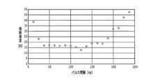
図7は試験用基板11がサファイア基板から構成される場合であり、図7からサファイア基板11の破断強度の最小値は、パルス間隔(ns)が20nsの場合であると算出できる。図9は試験用基板11として合成シリカを採用した場合であり、この場合の破断強度が最小となるパルス時間間隔(ns)は125nsであると算出できる。 FIG. 7 shows a case where the
上述したシールドトンネル形成工程、破断強度測定工程及び最小値算出工程を実施することにより、ウェーハをレーザー加工する際の最適なレーザー加工条件が算出されたことになる。 By carrying out the shield tunnel forming step, the breaking strength measuring step and the minimum value calculating step described above, the optimum laser processing conditions for laser processing the wafer are calculated.
即ち、試験用基板11としてサファイア基板を採用する場合には、バーストパルスレーザービームLB3の各パルスの時間間隔は20nsとするのが好ましい。このバーストパルスの時間間隔は、第1の間引き手段6により設定される。 That is, when a sapphire substrate is used as the
シールドトンネル形成工程のレーザー加工条件は、例えば次のように設定されている。 The laser processing conditions for the shield tunnel forming process are set as follows, for example.
レーザー発振器 :LD励起Qスイッチ Nd:フェムト秒YAGレーザー又はピコ秒YAGレーザー
波長 :1064nm
平均出力 :0.3W
バーストパルスの繰り返し周波数 :10kHz
集光スポット径 :φ1μm
加工送り速度 :100mm/s
バーストパルス数 :3Laser oscillator: LD excitation Q-switch Nd: femtosecond YAG laser or picosecond YAG laser Wavelength: 1064 nm
Average output: 0.3W
Burst pulse repetition frequency: 10 kHz
Condensing spot diameter: φ1 μm
Processing feed rate: 100 mm / s
Number of burst pulses: 3
このような最適なレーザー加工条件を設定してから、例えば、図9に示すような光デバイスウェーハ21のレーザー加工を実施する。光デバイスウェーハ21は、サファイア基板23上に窒化ガリウム(GaN)等のエピタキシャル層25が積層されて構成されている。 After setting such optimum laser processing conditions, for example, laser processing of the
サファイア基板23は例えば200μmの厚みを有しており、エピタキシャル層25は例えば5μmの厚みを有している。エピタキシャル層25にはLED等の複数の光デバイス29が格子状に形成された分割予定ライン27によって区画されて形成されている。 The
次に、図10を参照して、上述した最適なレーザー加工条件により光デバイスウェーハ21をレーザー加工するレーザー加工工程について説明する。光デバイスウェーハ21の表面に形成された光デバイス29を保護するために、光デバイスウェーハ21の表面21aに保護テープ48を貼着し、この保護テープ48側をレーザー加工装置40のチャックテーブル18で保持する。 Next, with reference to FIG. 10, a laser processing step of laser processing the
図10でバーストパルスレーザービーム照射ユニット42は、略円筒形状のケーシング44中に収容された図1に示すバーストパルスレーザービーム発生ユニット2と、ケーシング44の先端に取り付けられた集光器12とから構成される。 In FIG. 10, the burst pulse laser
ケーシング44にはアライメントを実施するための撮像ユニット46が取り付けられている。撮像ユニット46は通常の撮像素子と赤外線撮像素子を有している。本実施形態のレーザー加工工程では、バーストパルスレーザービームLB3を光デバイスウェーハ21の裏面21b側から照射するため、撮像ユニット46の赤外線撮像素子により光デバイスウェーハ21を裏面21b側から撮像して分割予定ライン27を検出し、分割予定ライン27と集光器12とをX軸方向に整列させるアライメントを実施する。 An
アライメント実施後、最小値算出工程で算出されたパルスの時間間隔を有するバーストパルスレーザービームLB3の集光領域を光デバイスウェーハ21の分割予定ライン27に対応する内部に位置付けて、バーストパルスレーザービームLB3を光デバイスウェーハ21に照射し、チャックテーブル18をX軸方向に加工送りすることにより、分割予定ライン27に対応する光デバイスウェーハ21の内部に細孔とこの細孔を囲繞する非晶質とからなる複数のシールドトンネルを形成する。 After the alignment is performed, the focused region of the burst pulse laser beam LB3 having the pulse time interval calculated in the minimum value calculation step is positioned inside corresponding to the scheduled
チャックテーブル18をY軸方向に分割予定ライン27のピッチずつ割り出し送りしながら第1の方向に伸長する分割予定ライン27に沿ってシールドトンネルを形成するレーザー加工工程を実施する。次いで、チャックテーブル18を90°回転してから、第2の方向に伸長する分割予定ライン27に沿って同様なシールドトンネルを形成するレーザー加工工程を実施する。 A laser machining step of forming a shield tunnel along the scheduled
全ての分割予定ライン27に沿ってレーザー加工工程を実施した後、例えば図6に示すような、分割装置28を使用して光デバイスウェーハ21を分割予定ライン27に沿って割断し、全ての分割予定ライン27を割断することにより、光デバイスウェーハ21を個々のデバイスチップに分割する。 After performing the laser processing step along all the planned division lines 27, the
この分割工程を実施する装置は、図6に示すような分割装置28に限定されるものではなく、例えば特許第6151557号広報に開示された拡張ドラムを有する分割装置を使用するようにしてもよい。 The device for carrying out this division step is not limited to the
上述した実施形態では、被加工物として光デバイスウェーハを採用した例について説明したが、本発明のレーザー加工方法はこれに限定されることはなく、シリコンウェーハ、ガリウムヒ素ウェーハ等の他の被加工物にも同様に適用できる。 In the above-described embodiment, an example in which an optical device wafer is used as the workpiece has been described, but the laser machining method of the present invention is not limited to this, and other workpieces such as silicon wafers and gallium arsenide wafers are to be machined. It can be applied to things as well.
被加工物がシリコンウェーハの場合には、試験用基板11がシリコン基板から構成され、被加工物がガリウムヒ素ウェーハの場合には、試験用基板11がガリウムヒ素基板から構成される。 When the workpiece is a silicon wafer, the
2 バーストパルスレーザービーム発生ユニット
4 レーザー発振器
6 第1の間引き手段
8 増幅器
10 第2の間引き手段
11 試験用基板
12 集光器
14 ミラー
16 集光レンズ
20,20a,20b バーストパルス
21 光デバイスウェーハ
22 シールドトンネル
23 サファイア基板
24 細孔
25 エピタキシャル層
26 非晶質
27 分割予定ライン
28 分割装置
29 光デバイス
30 支持台
32 楔
34 破断強度測定器
42 バーストパルスレーザービーム照射ユニット
46 撮像ユニット
48 保護テープ2 Burst pulse laser beam generation unit 4
Claims (2)
Translated fromJapaneseレーザー発振器から発振され、該ウェーハに対して透過性を有する波長のパルスレーザービームのパルスを第1の間引き手段により第1の所定間隔で間引くパルス間引き工程と、
該パルス間引き工程実施後のパルスレーザービームを増幅する増幅工程と、
該増幅工程で増幅されたパルスレーザービームを第2の間引き手段により第2の所定間隔で連続して且つ間欠的に間引いてバーストパルスレーザービームを生成するバーストパルスレーザービーム生成工程と、
該ウェーハの前記基板と同一の材質及び厚みを有する試験用基板を準備する試験用基板準備工程と、
該試験用基板をレーザー加工装置のチャックテーブルで保持し、該バーストパルスレーザービームを構成する複数のパルスの時間間隔を変更しながら、該バーストパルスレーザービームの集光領域を該試験用基板の内部に位置付けて該バーストパルスレーザービームを該試験用基板に照射し、該チャックテーブルを加工送りすることにより、細孔と該細孔を囲繞する非晶質とからなる複数のシールドトンネルを直線的に所定間隔で該試験用基板内部に形成するシールドトンネル形成工程と、
該シールドトンネル形成工程を実施した後、該試験用基板を該複数のシールドトンネルに沿って破断する際の破断強度を測定する破断強度測定工程と、
該破断強度測定工程を該バーストパルスレーザービームを構成する複数のパルスの時間間隔を変更しながら複数回実施した後、該試験用基板の破断強度が最小となるパルスの時間間隔を算出する最小値算出工程と、
該最小値算出工程を実施した後、該ウェーハをレーザー加工装置の該チャックテーブルで保持し、該最小値算出工程で算出されたパルスの時間間隔を有するバーストパルスレーザービームの集光領域を該ウェーハの該分割予定ラインに対応する内部に位置付けて該バーストパルスレーザービームを該ウェーハに照射し、該チャックテーブルを加工送りすることにより、該分割予定ラインに対応する該ウェーハの内部に細孔と該細孔を囲繞する非晶質とからなる複数のシールドトンネルを直線的に所定間隔で形成するレーザー加工工程と、
を備えたことを特徴とするウェーハのレーザー加工方法。A laser machining method for a wafer in which an epitaxial layer is laminated on the surface of a substrate, and a device is formed in each region partitioned by a plurality of planned division lines intersecting the surface of the epitaxial layer.
A pulse thinning step of thinning out pulses of a pulsed laser beam having a wavelength oscillated from a laser oscillator and having a wavelength transparent to the wafer by a first thinning means at a first predetermined interval.
An amplification step that amplifies the pulsed laser beam after the pulse thinning step is performed, and
A burst pulse laser beam generation step of generating a burst pulse laser beam by continuously and intermittently thinning the pulsed laser beam amplified in the amplification step by a second thinning means at a second predetermined interval.
A test substrate preparation step for preparing a test substrate having the same material and thickness as the substrate of the wafer, and a test substrate preparation step.
The test substrate is held by the chuck table of the laser processing apparatus, and the focusing region of the burst pulse laser beam is set inside the test substrate while changing the time interval of a plurality of pulses constituting the burst pulse laser beam. By irradiating the test substrate with the burst pulse laser beam and processing and feeding the chuck table, a plurality of shield tunnels composed of pores and amorphous surrounding the pores are linearly formed. A shield tunnel forming step of forming the inside of the test substrate at predetermined intervals, and
After carrying out the shield tunnel forming step, a breaking strength measuring step for measuring the breaking strength when the test substrate is broken along the plurality of shield tunnels, and a breaking strength measuring step.
After performing the breaking intensity measuring step a plurality of times while changing the time intervals of the plurality of pulses constituting the burst pulse laser beam, the minimum value for calculating the pulse time interval at which the breaking intensity of the test substrate is minimized. Calculation process and
After performing the minimum value calculation step, the wafer is held by the chuck table of the laser processing apparatus, and the focused region of the burst pulse laser beam having the pulse time interval calculated in the minimum value calculation step is defined as the wafer. By irradiating the wafer with the burst pulse laser beam and processing and feeding the chuck table, the pores and the pores are formed inside the wafer corresponding to the planned division line. A laser processing process in which a plurality of shield tunnels composed of amorphous surrounding pores are linearly formed at predetermined intervals, and
A laser machining method for wafers, which is characterized by being equipped with.
レーザー発振器から発振され、該ウェーハに対して透過性を有する波長のパルスレーザービームを増幅する増幅工程と、
該増幅工程で増幅されたパルスレーザービームを間引き手段により所定間隔で連続して且つ間欠的に間引いてバーストパルスレーザービームを生成するバーストパルスレーザービーム生成工程と、
該ウェーハの前記基板と同一の材質及び厚みを有する試験用基板を準備する試験用基板準備工程と、
該試験用基板をレーザー加工装置のチャックテーブルで保持し、該バーストパルスレーザービームの集光領域を該試験用基板の内部に位置付けて該バーストパルスレーザービームを該試験用基板に照射し、該チャックテーブルを加工送りすることにより、細孔と該細孔を囲繞する非晶質とからなる複数のシールドトンネルを直線的に所定間隔で該試験用基板内部に形成するシールドトンネル形成工程と、
該シールドトンネル形成工程を実施した後、該試験用基板を該複数のシールドトンネルに沿って破断する際の破断強度を測定する破断強度測定工程と、
該破断強度測定工程を該バーストパルスレーザービームを構成する複数のパルスの時間間隔を変更しながら複数回実施した後、該試験用基板の破断強度が最小となるパルスの時間間隔を算出する最小値算出工程と、
該最小値算出工程を実施した後、該ウェーハをレーザー加工装置の該チャックテーブルで保持し、該最小値算出工程で算出された時間間隔を有するパルスを発振するレーザー発振器を使用して、該バーストパルスレーザービームの集光領域を該ウェーハの該分割予定ラインに対応する内部に位置付けて該バーストパルスレーザービームを該ウェーハに照射し、該チャックテーブルを加工送りすることにより、該分割予定ラインに対応する該ウェーハの内部に細孔と該細孔を囲繞する非晶質とからなる複数のシールドトンネルを直線的に所定間隔で形成するレーザー加工工程と、
を備えたことを特徴とするウェーハのレーザー加工方法。A laser machining method for a wafer in which an epitaxial layer is laminated on the surface of a substrate, and a device is formed in each region partitioned by a plurality of planned division lines intersecting the surface of the epitaxial layer.
An amplification step that oscillates from a laser oscillator and amplifies a pulsed laser beam with a wavelength that is transparent to the wafer.
A burst pulse laser beam generation step of generating a burst pulse laser beam by continuously and intermittently thinning the pulsed laser beam amplified in the amplification step by a thinning means at predetermined intervals.
A test substrate preparation step for preparing a test substrate having the same material and thickness as the substrate of the wafer, and a test substrate preparation step.
The test substrate is held by a chuck table of a laser processing apparatus, the condensing region of the burst pulse laser beam is positioned inside the test substrate, the burst pulse laser beam is irradiated to the test substrate, and the chuck is used. A shield tunnel forming step of linearly forming a plurality of shield tunnels composed of pores and amorphous surrounding the pores inside the test substrate at predetermined intervals by processing and feeding the table.
After carrying out the shield tunnel forming step, a breaking strength measuring step for measuring the breaking strength when the test substrate is broken along the plurality of shield tunnels, and a breaking strength measuring step.
After performing the breaking intensity measuring step a plurality of times while changing the time intervals of the plurality of pulses constituting the burst pulse laser beam, the minimum value for calculating the pulse time interval at which the breaking intensity of the test substrate is minimized. Calculation process and
After performing the minimum value calculation step, the burst is held by holding the wafer on the chuck table of the laser processing apparatus and using a laser oscillator that oscillates a pulse having a time interval calculated in the minimum value calculation step. The focused region of the pulsed laser beam is positioned inside the wafer corresponding to the planned division line, the wafer is irradiated with the burst pulse laser beam, and the chuck table is processed and fed to correspond to the planned division line. A laser processing step of linearly forming a plurality of shield tunnels composed of pores and amorphous surrounding the pores at predetermined intervals inside the wafer.
A laser machining method for wafers, which is characterized by being equipped with.
Priority Applications (7)
| Application Number | Priority Date | Filing Date | Title |
|---|---|---|---|
| JP2017230283AJP6925745B2 (en) | 2017-11-30 | 2017-11-30 | Wafer laser machining method |
| KR1020180129964AKR102525264B1 (en) | 2017-11-30 | 2018-10-29 | Laser machining method of wafer |
| MYPI2018704262AMY196219A (en) | 2017-11-30 | 2018-11-13 | Laser Processing Method For Wafer |
| US16/195,190US10573559B2 (en) | 2017-11-30 | 2018-11-19 | Laser processing method for wafer |
| CN201811422874.0ACN109848577B (en) | 2017-11-30 | 2018-11-27 | Laser processing method for wafer |
| TW107142249ATWI771533B (en) | 2017-11-30 | 2018-11-27 | Wafer laser processing method |
| DE102018220595.7ADE102018220595B4 (en) | 2017-11-30 | 2018-11-29 | Laser processing method for a wafer |
Applications Claiming Priority (1)
| Application Number | Priority Date | Filing Date | Title |
|---|---|---|---|
| JP2017230283AJP6925745B2 (en) | 2017-11-30 | 2017-11-30 | Wafer laser machining method |
Publications (2)
| Publication Number | Publication Date |
|---|---|
| JP2019098359A JP2019098359A (en) | 2019-06-24 |
| JP6925745B2true JP6925745B2 (en) | 2021-08-25 |
Family
ID=66547918
Family Applications (1)
| Application Number | Title | Priority Date | Filing Date |
|---|---|---|---|
| JP2017230283AActiveJP6925745B2 (en) | 2017-11-30 | 2017-11-30 | Wafer laser machining method |
Country Status (7)
| Country | Link |
|---|---|
| US (1) | US10573559B2 (en) |
| JP (1) | JP6925745B2 (en) |
| KR (1) | KR102525264B1 (en) |
| CN (1) | CN109848577B (en) |
| DE (1) | DE102018220595B4 (en) |
| MY (1) | MY196219A (en) |
| TW (1) | TWI771533B (en) |
Families Citing this family (8)
| Publication number | Priority date | Publication date | Assignee | Title |
|---|---|---|---|---|
| JP2020150224A (en)* | 2019-03-15 | 2020-09-17 | キオクシア株式会社 | Semiconductor device |
| JP7339031B2 (en)* | 2019-06-28 | 2023-09-05 | 株式会社ディスコ | Laser processing equipment |
| JP7286464B2 (en)* | 2019-08-02 | 2023-06-05 | 株式会社ディスコ | Laser processing equipment |
| US12329832B2 (en) | 2019-09-10 | 2025-06-17 | Gc Corporation | Dental polymerizable composition |
| JP7507599B2 (en)* | 2020-05-12 | 2024-06-28 | 株式会社ディスコ | Laser processing method |
| DE102020128595A1 (en)* | 2020-10-30 | 2022-05-05 | Eissmann Automotive Deutschland Gmbh | Method of providing weaknesses in a decorative material |
| CN112635309B (en)* | 2020-12-07 | 2024-07-12 | 福建晶安光电有限公司 | Substrate processing method and substrate processed by the method |
| JP2023102809A (en)* | 2022-01-13 | 2023-07-26 | 株式会社ディスコ | Manufacturing method of substrate |
Family Cites Families (29)
| Publication number | Priority date | Publication date | Assignee | Title |
|---|---|---|---|---|
| US4197346A (en) | 1978-10-10 | 1980-04-08 | Appleton Papers Inc. | Self-contained pressure-sensitive record material and process of preparation |
| JPS6151557A (en) | 1984-08-21 | 1986-03-14 | Ngk Spark Plug Co Ltd | Reinforced solid electrolyte function element |
| TW297138B (en)* | 1995-05-31 | 1997-02-01 | Handotai Energy Kenkyusho Kk | |
| US6736988B1 (en)* | 1999-11-04 | 2004-05-18 | Mitsubishi Gas Chemical Company, Inc. | Copper-clad board suitable for making hole with carbon dioxide laser, method of making hole in said copper-clad board and printed wiring board comprising said copper-clad board |
| WO2005029546A2 (en)* | 2003-09-16 | 2005-03-31 | The Trustees Of Columbia University In The City Of New York | Method and system for providing a continuous motion sequential lateral solidification for reducing or eliminating artifacts, and a mask for facilitating such artifact reduction/elimination |
| US7364952B2 (en)* | 2003-09-16 | 2008-04-29 | The Trustees Of Columbia University In The City Of New York | Systems and methods for processing thin films |
| JP2005129607A (en) | 2003-10-22 | 2005-05-19 | Disco Abrasive Syst Ltd | Wafer division method |
| JP2005142303A (en)* | 2003-11-05 | 2005-06-02 | Disco Abrasive Syst Ltd | Silicon wafer dividing method and apparatus |
| US20060191884A1 (en)* | 2005-01-21 | 2006-08-31 | Johnson Shepard D | High-speed, precise, laser-based material processing method and system |
| JP2007149743A (en)* | 2005-11-24 | 2007-06-14 | Disco Abrasive Syst Ltd | Wafer laser processing method |
| JP2010183014A (en)* | 2009-02-09 | 2010-08-19 | Disco Abrasive Syst Ltd | Method of processing wafer |
| US10307862B2 (en)* | 2009-03-27 | 2019-06-04 | Electro Scientific Industries, Inc | Laser micromachining with tailored bursts of short laser pulses |
| JP6121901B2 (en)* | 2010-07-12 | 2017-04-26 | ロフィン−シナー テクノロジーズ インコーポレーテッド | Material processing by laser filament formation |
| JP5910075B2 (en)* | 2011-12-27 | 2016-04-27 | 三星ダイヤモンド工業株式会社 | Workpiece processing method |
| AU2013222069A1 (en)* | 2012-02-26 | 2014-10-16 | Solexel, Inc. | Systems and methods for laser splitting and device layer transfer |
| JP2014104484A (en)* | 2012-11-27 | 2014-06-09 | Disco Abrasive Syst Ltd | Laser processing apparatus |
| JP6208430B2 (en)* | 2013-01-25 | 2017-10-04 | 株式会社ディスコ | Laser processing method |
| TWI543833B (en)* | 2013-01-28 | 2016-08-01 | 先進科技新加坡有限公司 | Method of radiatively grooving a semiconductor substrate |
| JP6151557B2 (en) | 2013-05-13 | 2017-06-21 | 株式会社ディスコ | Laser processing method |
| US20150034613A1 (en)* | 2013-08-02 | 2015-02-05 | Rofin-Sinar Technologies Inc. | System for performing laser filamentation within transparent materials |
| US10144088B2 (en)* | 2013-12-03 | 2018-12-04 | Rofin-Sinar Technologies Llc | Method and apparatus for laser processing of silicon by filamentation of burst ultrafast laser pulses |
| US9850160B2 (en)* | 2013-12-17 | 2017-12-26 | Corning Incorporated | Laser cutting of display glass compositions |
| KR20170028943A (en)* | 2014-07-14 | 2017-03-14 | 코닝 인코포레이티드 | System for and method of processing transparent materials using laser beam focal lines adjustable in length and diameter |
| JP6548944B2 (en)* | 2015-04-09 | 2019-07-24 | 株式会社ディスコ | Laser processing equipment |
| JP6600254B2 (en)* | 2015-12-28 | 2019-10-30 | 株式会社ディスコ | Wafer processing method |
| JP6598702B2 (en)* | 2016-02-16 | 2019-10-30 | 株式会社ディスコ | Wafer processing method |
| JP2017204574A (en)* | 2016-05-12 | 2017-11-16 | 株式会社ディスコ | Processing method and laser processing apparatus of sapphire wafer |
| JP6755707B2 (en)* | 2016-05-12 | 2020-09-16 | 株式会社ディスコ | Laser processing equipment |
| US10363629B2 (en)* | 2017-06-01 | 2019-07-30 | Applied Materials, Inc. | Mitigation of particle contamination for wafer dicing processes |
- 2017
- 2017-11-30JPJP2017230283Apatent/JP6925745B2/enactiveActive
- 2018
- 2018-10-29KRKR1020180129964Apatent/KR102525264B1/enactiveActive
- 2018-11-13MYMYPI2018704262Apatent/MY196219A/enunknown
- 2018-11-19USUS16/195,190patent/US10573559B2/enactiveActive
- 2018-11-27TWTW107142249Apatent/TWI771533B/enactive
- 2018-11-27CNCN201811422874.0Apatent/CN109848577B/enactiveActive
- 2018-11-29DEDE102018220595.7Apatent/DE102018220595B4/enactiveActive
Also Published As
| Publication number | Publication date |
|---|---|
| KR102525264B1 (en) | 2023-04-24 |
| US10573559B2 (en) | 2020-02-25 |
| KR20190064434A (en) | 2019-06-10 |
| MY196219A (en) | 2023-03-23 |
| DE102018220595B4 (en) | 2021-07-15 |
| TW201924838A (en) | 2019-07-01 |
| JP2019098359A (en) | 2019-06-24 |
| CN109848577B (en) | 2021-11-16 |
| CN109848577A (en) | 2019-06-07 |
| DE102018220595A1 (en) | 2019-06-06 |
| TWI771533B (en) | 2022-07-21 |
| US20190164833A1 (en) | 2019-05-30 |
Similar Documents
| Publication | Publication Date | Title |
|---|---|---|
| JP6925745B2 (en) | Wafer laser machining method | |
| JP4418282B2 (en) | Laser processing method | |
| US6841482B2 (en) | Laser machining of semiconductor materials | |
| JP4478184B2 (en) | Laser cleaving method and laser processing apparatus | |
| JP5620669B2 (en) | Laser dicing method and laser dicing apparatus | |
| US20110174787A1 (en) | Laser dicing apparatus | |
| TW201631228A (en) | Wafer producing method | |
| TW201639016A (en) | Wafer generation method | |
| CN103223558A (en) | Laser processing apparatus | |
| CN110039204B (en) | Laser processing method of workpiece | |
| TWI726656B (en) | Optimised laser cutting | |
| JP5596750B2 (en) | Laser dicing method | |
| TWI705868B (en) | Wafer production method | |
| US9174306B2 (en) | Laser processing method for nonlinear crystal substrate | |
| US10692740B2 (en) | Laser processing apparatus | |
| KR102391850B1 (en) | Laser machining apparatus | |
| JP2005288501A (en) | Laser processing method and apparatus | |
| JP2006082232A (en) | Laser processing method | |
| JP2016013571A (en) | Laser processing device and laser processing method | |
| JP6529414B2 (en) | Wafer processing method | |
| JP2024094718A (en) | Laser processing equipment | |
| JP2023148049A (en) | Laser processing method | |
| IES20010945A2 (en) | Laser machining of semiconductor material | |
| JP2013010123A (en) | Laser processing device |
Legal Events
| Date | Code | Title | Description |
|---|---|---|---|
| A621 | Written request for application examination | Free format text:JAPANESE INTERMEDIATE CODE: A621 Effective date:20200914 | |
| A977 | Report on retrieval | Free format text:JAPANESE INTERMEDIATE CODE: A971007 Effective date:20210630 | |
| TRDD | Decision of grant or rejection written | ||
| A01 | Written decision to grant a patent or to grant a registration (utility model) | Free format text:JAPANESE INTERMEDIATE CODE: A01 Effective date:20210803 | |
| A61 | First payment of annual fees (during grant procedure) | Free format text:JAPANESE INTERMEDIATE CODE: A61 Effective date:20210803 | |
| R150 | Certificate of patent or registration of utility model | Ref document number:6925745 Country of ref document:JP Free format text:JAPANESE INTERMEDIATE CODE: R150 | |
| R250 | Receipt of annual fees | Free format text:JAPANESE INTERMEDIATE CODE: R250 | |
| R250 | Receipt of annual fees | Free format text:JAPANESE INTERMEDIATE CODE: R250 |