JP6920405B2 - Coded microflakes - Google Patents
Coded microflakesDownload PDFInfo
- Publication number
- JP6920405B2 JP6920405B2JP2019220042AJP2019220042AJP6920405B2JP 6920405 B2JP6920405 B2JP 6920405B2JP 2019220042 AJP2019220042 AJP 2019220042AJP 2019220042 AJP2019220042 AJP 2019220042AJP 6920405 B2JP6920405 B2JP 6920405B2
- Authority
- JP
- Japan
- Prior art keywords
- microflake
- microflakes
- binary sequence
- type
- notch
- Prior art date
- Legal status (The legal status is an assumption and is not a legal conclusion. Google has not performed a legal analysis and makes no representation as to the accuracy of the status listed.)
- Active
Links
Images


Classifications
- G—PHYSICS
- G01—MEASURING; TESTING
- G01N—INVESTIGATING OR ANALYSING MATERIALS BY DETERMINING THEIR CHEMICAL OR PHYSICAL PROPERTIES
- G01N33/00—Investigating or analysing materials by specific methods not covered by groups G01N1/00 - G01N31/00
- G01N33/48—Biological material, e.g. blood, urine; Haemocytometers
- G01N33/50—Chemical analysis of biological material, e.g. blood, urine; Testing involving biospecific ligand binding methods; Immunological testing
- G01N33/53—Immunoassay; Biospecific binding assay; Materials therefor
- G01N33/543—Immunoassay; Biospecific binding assay; Materials therefor with an insoluble carrier for immobilising immunochemicals
- G01N33/54313—Immunoassay; Biospecific binding assay; Materials therefor with an insoluble carrier for immobilising immunochemicals the carrier being characterised by its particulate form
- G01N33/54326—Magnetic particles
- G—PHYSICS
- G01—MEASURING; TESTING
- G01N—INVESTIGATING OR ANALYSING MATERIALS BY DETERMINING THEIR CHEMICAL OR PHYSICAL PROPERTIES
- G01N33/00—Investigating or analysing materials by specific methods not covered by groups G01N1/00 - G01N31/00
- G01N33/48—Biological material, e.g. blood, urine; Haemocytometers
- G01N33/50—Chemical analysis of biological material, e.g. blood, urine; Testing involving biospecific ligand binding methods; Immunological testing
- G01N33/53—Immunoassay; Biospecific binding assay; Materials therefor
- G01N33/543—Immunoassay; Biospecific binding assay; Materials therefor with an insoluble carrier for immobilising immunochemicals
- G01N33/54313—Immunoassay; Biospecific binding assay; Materials therefor with an insoluble carrier for immobilising immunochemicals the carrier being characterised by its particulate form
- C—CHEMISTRY; METALLURGY
- C12—BIOCHEMISTRY; BEER; SPIRITS; WINE; VINEGAR; MICROBIOLOGY; ENZYMOLOGY; MUTATION OR GENETIC ENGINEERING
- C12Q—MEASURING OR TESTING PROCESSES INVOLVING ENZYMES, NUCLEIC ACIDS OR MICROORGANISMS; COMPOSITIONS OR TEST PAPERS THEREFOR; PROCESSES OF PREPARING SUCH COMPOSITIONS; CONDITION-RESPONSIVE CONTROL IN MICROBIOLOGICAL OR ENZYMOLOGICAL PROCESSES
- C12Q1/00—Measuring or testing processes involving enzymes, nucleic acids or microorganisms; Compositions therefor; Processes of preparing such compositions
- C12Q1/68—Measuring or testing processes involving enzymes, nucleic acids or microorganisms; Compositions therefor; Processes of preparing such compositions involving nucleic acids
- C12Q1/6813—Hybridisation assays
- C12Q1/6834—Enzymatic or biochemical coupling of nucleic acids to a solid phase
- C12Q1/6837—Enzymatic or biochemical coupling of nucleic acids to a solid phase using probe arrays or probe chips
- G—PHYSICS
- G01—MEASURING; TESTING
- G01N—INVESTIGATING OR ANALYSING MATERIALS BY DETERMINING THEIR CHEMICAL OR PHYSICAL PROPERTIES
- G01N33/00—Investigating or analysing materials by specific methods not covered by groups G01N1/00 - G01N31/00
- G01N33/48—Biological material, e.g. blood, urine; Haemocytometers
- G01N33/50—Chemical analysis of biological material, e.g. blood, urine; Testing involving biospecific ligand binding methods; Immunological testing
- G01N33/53—Immunoassay; Biospecific binding assay; Materials therefor
- G01N33/543—Immunoassay; Biospecific binding assay; Materials therefor with an insoluble carrier for immobilising immunochemicals
- G01N33/54366—Apparatus specially adapted for solid-phase testing
- G01N33/54386—Analytical elements
- G01N33/54387—Immunochromatographic test strips
- G—PHYSICS
- G01—MEASURING; TESTING
- G01N—INVESTIGATING OR ANALYSING MATERIALS BY DETERMINING THEIR CHEMICAL OR PHYSICAL PROPERTIES
- G01N33/00—Investigating or analysing materials by specific methods not covered by groups G01N1/00 - G01N31/00
- G01N33/48—Biological material, e.g. blood, urine; Haemocytometers
- G01N33/50—Chemical analysis of biological material, e.g. blood, urine; Testing involving biospecific ligand binding methods; Immunological testing
- G01N33/53—Immunoassay; Biospecific binding assay; Materials therefor
- G01N33/543—Immunoassay; Biospecific binding assay; Materials therefor with an insoluble carrier for immobilising immunochemicals
- G01N33/551—Immunoassay; Biospecific binding assay; Materials therefor with an insoluble carrier for immobilising immunochemicals the carrier being inorganic
- G01N33/553—Metal or metal coated
- G—PHYSICS
- G01—MEASURING; TESTING
- G01N—INVESTIGATING OR ANALYSING MATERIALS BY DETERMINING THEIR CHEMICAL OR PHYSICAL PROPERTIES
- G01N33/00—Investigating or analysing materials by specific methods not covered by groups G01N1/00 - G01N31/00
- G01N33/48—Biological material, e.g. blood, urine; Haemocytometers
- G01N33/50—Chemical analysis of biological material, e.g. blood, urine; Testing involving biospecific ligand binding methods; Immunological testing
- G01N33/68—Chemical analysis of biological material, e.g. blood, urine; Testing involving biospecific ligand binding methods; Immunological testing involving proteins, peptides or amino acids
- G01N33/6803—General methods of protein analysis not limited to specific proteins or families of proteins
- H—ELECTRICITY
- H01—ELECTRIC ELEMENTS
- H01L—SEMICONDUCTOR DEVICES NOT COVERED BY CLASS H10
- H01L22/00—Testing or measuring during manufacture or treatment; Reliability measurements, i.e. testing of parts without further processing to modify the parts as such; Structural arrangements therefor
- H01L22/10—Measuring as part of the manufacturing process
Landscapes
- Health & Medical Sciences (AREA)
- Life Sciences & Earth Sciences (AREA)
- Engineering & Computer Science (AREA)
- Immunology (AREA)
- Chemical & Material Sciences (AREA)
- Molecular Biology (AREA)
- Biomedical Technology (AREA)
- Hematology (AREA)
- Urology & Nephrology (AREA)
- Physics & Mathematics (AREA)
- Analytical Chemistry (AREA)
- Biotechnology (AREA)
- Microbiology (AREA)
- General Health & Medical Sciences (AREA)
- Biochemistry (AREA)
- General Physics & Mathematics (AREA)
- Food Science & Technology (AREA)
- Cell Biology (AREA)
- Pathology (AREA)
- Medicinal Chemistry (AREA)
- Organic Chemistry (AREA)
- Proteomics, Peptides & Aminoacids (AREA)
- Wood Science & Technology (AREA)
- Zoology (AREA)
- Biophysics (AREA)
- Bioinformatics & Cheminformatics (AREA)
- Manufacturing & Machinery (AREA)
- General Engineering & Computer Science (AREA)
- Genetics & Genomics (AREA)
- Inorganic Chemistry (AREA)
- Computer Hardware Design (AREA)
- Microelectronics & Electronic Packaging (AREA)
- Power Engineering (AREA)
- Bioinformatics & Computational Biology (AREA)
- Investigating, Analyzing Materials By Fluorescence Or Luminescence (AREA)
- Automatic Analysis And Handling Materials Therefor (AREA)
- Apparatus Associated With Microorganisms And Enzymes (AREA)
Description
Translated fromJapanese(関連出願の相互参照)
本出願は2018年12月6日に出願された米国仮出願第62/776,224号の利益を主張し、その全体が参照により本明細書に組み込まれる。(Cross-reference of related applications)
This application claims the interests of US Provisional Application No. 62 / 776,224 filed December 6, 2018, which is incorporated herein by reference in its entirety.
(技術分野)
本発明の実施形態は、デジタルコードでコード化されたマイクロフレークおよびマイクロフレークの製造プロセスに関する。(Technical field)
Embodiments of the present invention relate to digitally coded microflakes and processes for manufacturing microflakes.
(背景)
精密医療、個別化医療および予防医療の開発に伴い、生体試験サンプル中の多数の標的に対するアッセイを実施するためのインビトロ診断(IVD)の分野における必要性が存在する。多重アッセイとして知られる多重アプローチは試験情報量を増加させコストを減少させるために、複数の異なる標的に対して複数の測定を同時に行うことを可能にする。多重アッセイは病理学的診断(例えば感染症または腫瘍学)、食品安全性、ヒトおよび動物の疾患制御、環境モニタリング、バイオメディカルサイエンス研究、薬物スクリーニングおよび発見などのような広範囲の適用を有する。(background)
With the development of precision medicine, personalized medicine and preventive medicine, there is a need in the field of in vitro diagnostics (IVD) to perform assays against a large number of targets in biometric samples. A multiplex approach, known as a multiplex assay, allows multiple measurements to be made simultaneously for multiple different targets in order to increase the amount of test information and reduce costs. Multiple assays have a wide range of applications such as pathological diagnosis (eg, infectious disease or oncology), food safety, human and animal disease control, environmental monitoring, biomedical science research, drug screening and discovery.
多重アッセイを行うために、プローブのような試薬をマイクロキャリアの固相表面に固定化する。所望の標的の型によってプローブは抗体、タンパク質、抗原、DNA、RNAまたは所望の標的に対する親和性を有する別のモジュールになり得る。異なるプローブを有するマイクロキャリアは試験サンプル中に添加され、その結果プローブおよび試験サンプル中の対応する標的は特定結合を形成する。プローブに結合していない過剰な物質を洗浄し除去することができる。検出抗体または他の適切な薬剤を標的に添加して特定結合を形成することができる。これらの検出抗体または適切な薬剤は光源による励起の際に発光するフルオロフォアを含み得る。発光された光はプローブに結合された標的を観察し定量化することを可能にする。 To perform the multiplex assay, reagents such as probes are immobilized on the solid phase surface of the microcarriers. Depending on the type of target desired, the probe can be an antibody, protein, antigen, DNA, RNA or another module with affinity for the desired target. Microcarriers with different probes are added into the test sample so that the probe and the corresponding target in the test sample form a specific bond. Excess substances that are not bound to the probe can be washed and removed. A detection antibody or other suitable agent can be added to the target to form a specific bond. These detection antibodies or suitable agents may include fluorophores that emit light when excited by a light source. The emitted light makes it possible to observe and quantify the target bound to the probe.
多重アッセイにおける試験サンプルは典型的には関心のある複数の標的を含む。どの標的がマイクロキャリア上のプローブに結合しているかを追跡するために、異なるプローブを有するマイクロキャリアが互いに区別され得るように、マイクロキャリアをコード化するための様々なアプローチが開発されてきた。 Test samples in multiple assays typically contain multiple targets of interest. Various approaches have been developed to encode microcarriers so that microcarriers with different probes can be distinguished from each other in order to track which targets are bound to probes on the microcarriers.
例えば1つのアプローチは異なる蛍光色素で異なるマイクロキャリアを標識することである;しかし利用可能な蛍光色素の数は典型的には高い情報量が所望される多重アッセイには不十分である。別のアプローチは不透明セグメントおよび透明ギャップのパターンを有するマイクロキャリアをコード化することであり、この場合パターンはマイクロキャリア内に含まれる。 For example, one approach is to label different microcarriers with different fluorochromes; but the number of fluorochromes available is typically insufficient for multiple assays where high information levels are desired. Another approach is to encode microcarriers with a pattern of opaque segments and transparent gaps, in which case the pattern is contained within the microcarriers.
上述のような従来のアプローチは一般に製造コストが高く、反応表面が不十分で性能が悪い等のいくつかの欠点を有する。したがってコード化されたマイクロキャリアの設計および製造を改善する必要がある。 The conventional approach as described above generally has some drawbacks such as high manufacturing cost, insufficient reaction surface and poor performance. Therefore, there is a need to improve the design and manufacture of coded microcarriers.
一実施形態では、マイクロフレークが提供される。マイクロフレークは上面と上面に実質的に平行な下面とを有するポリマー層を含む。上面および下面の少なくとも1つは、標的分析物と結合するために標的特定プローブに結合される。マイクロフレークは上面および下面に実質的に平行な平面上のエッジアウトラインによってコード化された2進シーケンスのビットによって識別される。2進シーケンス内のビットはエッジアウトラインを取り囲むそれぞれの所定の位置でコード化される。 In one embodiment, microflakes are provided. Microflakes include a polymer layer having an upper surface and a lower surface substantially parallel to the upper surface. At least one of the top and bottom surfaces is attached to the targeting probe to bind to the target analyte. Microflakes are identified by bits in a binary sequence encoded by an edge outline on a plane that is substantially parallel to the top and bottom surfaces. The bits in the binary sequence are encoded in their respective predetermined positions surrounding the edge outline.
別の実施形態では、多重アッセイのための装置が提供される。この装置は第1の標的検体への標的特定結合を形成するための第1のマイクロフレークと、第1の標的検体とは異なる第2の標的検体への標的特定結合を形成するための第2のマイクロフレークとを含む。第1のマイクロフレークは第1の2進シーケンスによって識別され、第2のマイクロフレークは第1の2進シーケンスとは異なる第2の2進シーケンスによって識別される。第1の2進シーケンスは第1のマイクロフレークの上面および下面に実質的に平行な第1の平面上の第1のエッジアウトラインによってコード化され、第1の2進シーケンス内のビットは第1のエッジアウトラインを取り囲むそれぞれの事前定義された位置でコード化される。第2の2進シーケンスは第2のマイクロフレークの上面および下面に実質的に平行な第2の平面上の第2のエッジアウトラインによってコード化され、第2の2進シーケンス内のビットは第2のエッジアウトラインを取り囲むそれぞれの事前定義された位置でコード化される。 In another embodiment, a device for multiple assays is provided. This device has a first microflake for forming a target-specific bond to a first target sample and a second for forming a target-specific bond to a second target sample different from the first target sample. Includes with microflakes. The first microflake is identified by a first binary sequence and the second microflake is identified by a second binary sequence that is different from the first binary sequence. The first binary sequence is encoded by a first edge outline on a first plane that is substantially parallel to the top and bottom surfaces of the first microflake, and the bits in the first binary sequence are the first. It is coded at each predefined position that surrounds the edge outline of. The second binary sequence is encoded by a second edge outline on a second plane that is substantially parallel to the top and bottom surfaces of the second microflake, and the bits in the second binary sequence are second. It is coded at each predefined position that surrounds the edge outline of.
さらに別の実施形態では半導体ウェーハが提供される。半導体ウェーハは基板と、基板上の複数の第1のマイクロフレークと、基板上の複数の第2のマイクロフレークとを含む。各第1のマイクロフレークは第1の2進シーケンスによって識別され、各第2のマイクロフレークは第1の2進シーケンスとは異なる第2の2進シーケンスによって識別される。各第1のマイクロフレークは基板に実質的に平行な平面上の第1のエッジアウトラインによってコード化された第1の2進シーケンスによって識別され、第1の2進シーケンス内のビットは第1のエッジアウトラインを取り囲むそれぞれの所定の位置でコード化される。各第2のマイクロフレークは平面上の第2のエッジアウトラインによってコード化された第2の2進シーケンスによって識別され、第2の2進シーケンス内のビットは第2のエッジアウトラインを取り囲むそれぞれの所定の位置でコード化される。 Yet another embodiment provides a semiconductor wafer. The semiconductor wafer includes a substrate, a plurality of first microflakes on the substrate, and a plurality of second microflakes on the substrate. Each first microflake is identified by a first binary sequence, and each second microflake is identified by a second binary sequence that is different from the first binary sequence. Each first microflake is identified by a first binary sequence encoded by a first edge outline on a plane substantially parallel to the substrate, with the bits in the first binary sequence being the first. It is coded in each predetermined position that surrounds the edge outline. Each second microflake is identified by a second binary sequence encoded by a second edge outline on the plane, with the bits in the second binary sequence each predetermined surrounding the second edge outline. It is coded at the position of.
他の態様および特徴は添付の図面と併せて以下の特定の実施形態の説明を検討することにより当業者には明らかになるであろう。 Other aspects and features will become apparent to those skilled in the art by examining the description of the particular embodiments below in conjunction with the accompanying drawings.
本発明は限定ではなく例として同様の参照コードが同様の要素を示す添付図面の図に示されている。本開示における、「an」または「one」という実施形態に対する異なる言及は必ずしも同じ実施形態に対するものではなく、そのような言及は少なくとも1つを意味することに留意されたい。また一実施形態に関連して特定の機能、構造または特徴が記載されている場合には、明示的に記載されているか否かにかかわらず、他の実施形態に関連して当該機能、構造または特徴を実施することが当業者の知る範囲内であることが提出される。 The present invention is not limited, but as an example, similar reference codes are shown in the accompanying drawings showing similar elements. It should be noted that different references to embodiments "an" or "one" in the present disclosure do not necessarily refer to the same embodiment, and such references mean at least one. In addition, when a specific function, structure or feature is described in relation to one embodiment, the function, structure or feature is described in relation to another embodiment, whether or not it is explicitly described. It is submitted that the implementation of the feature is within the knowledge of those skilled in the art.
(詳細な説明)
以下の記載では数多くの特定の詳細を記載する。しかし本発明の実施例をこうした特定の詳細なしで実施し得るということが分かる。他の例ではこの説明の理解を不明瞭にしないために周知の回路、構造、および技法は詳細に示されていない。しかし当業者であれば本発明はそのような特定の詳細なしに実施できることを理解するであろう。当業者は含まれる説明を用いて過度の実験なしに適切な機能を実施することができるであろう。(Detailed explanation)
The following description describes a number of specific details. However, it can be seen that embodiments of the present invention can be practiced without these particular details. In other examples, well-known circuits, structures, and techniques are not shown in detail to avoid obscuring the understanding of this description. However, those skilled in the art will appreciate that the invention can be practiced without such specific details. One of ordinary skill in the art will be able to perform the appropriate function without undue experimentation using the instructions provided.
本明細書中に記載されるのは多重アッセイにおける分析物検出および分析のためのキャリアとして使用され得るマイクロフレークである。いくつかの実施形態では、デジタル磁気フレークとも呼ばれるマイクロフレークは、それぞれのデジタル識別子(デジタルコードまたはコードとも呼ばれる)によって識別され得る。一実施形態では、マイクロフレークのデジタル識別子が連続したノッチおよびマイクロフレークの周辺部(すなわちエッジ)におけるエッジセグメントによってコード化される。マイクロフレークのエッジアウトラインを検出することによって検出器はマイクロフレークに関連するコードを識別することができる。より具体的にはマイクロフレークの上面および下面に実質的に平行な平面上でマイクロフレークの周囲の輪郭を描くエッジアウトラインにマイクロフレークを同定する2進シーケンスをコード化する。 Described herein are microflakes that can be used as carriers for analyte detection and analysis in multiple assays. In some embodiments, microflakes, also referred to as digital magnetic flakes, can be identified by their respective digital identifier (also referred to as a digital code or code). In one embodiment, the digital identifier of a microflake is encoded by a contiguous notch and an edge segment at the periphery (ie, edge) of the microflake. By detecting the edge outline of the microflake, the detector can identify the code associated with the microflake. More specifically, it encodes a binary sequence that identifies microflakes in an edge outline that outlines the perimeter of the microflakes on a plane that is substantially parallel to the top and bottom surfaces of the microflakes.
多重アッセイにおいて使用される場合、同じコードを有するマイクロフレークは同じ標的分析物を捕捉するために同じタイプのプローブに結合され、異なるコードを有するマイクロフレークは異なる標的分析物を捕捉するために異なるタイプのプローブに結合される。 When used in multiple assays, microflakes with the same code are bound to the same type of probe to capture the same target analyte, and microflakes with different codes are of different types to capture different target analytes. It is bound to the probe of.
一実施形態では、マイクロフレークは取扱いおよび収集を容易にするために磁気応答性材料を含むことができる。磁気応答性材料はマイクロフレークの実質的にすべて、マイクロフレークの一部、またはマイクロフレークのただ1つの成分を構成してもよい。マイクロフレークの残りはとりわけポリマー材料、コーティング、およびプローブの付着を可能にする部分を含み得る。磁気応答性材料の例としては鉄、ニッケル、コバルト、希土類金属の合金などの磁性金属が挙げられるが、これらに限定されない。一実施形態では、磁性金属ストリップがマイクロフレークの非磁性ポリマー層内に埋め込まれてもよい。非磁性ポリマー層は実質的に透明であってもよい。あるいはマイクロフレークが磁性フォトレジスト材料、例えば磁性粒子とポリマーとの混合物から作製されてもよい。磁気フォトレジスト材料は実質的に透明であってもよい。しかしながらマイクロフレークは前述の材料とは異なる材料から作製されてもよいことに留意されたい。 In one embodiment, the microflakes can include a magnetically responsive material for ease of handling and collection. The magnetically responsive material may constitute substantially all of the microflakes, part of the microflakes, or only one component of the microflakes. The rest of the microflakes may include, among other things, polymeric materials, coatings, and parts that allow the probe to adhere. Examples of magnetically responsive materials include, but are not limited to, magnetic metals such as iron, nickel, cobalt, and alloys of rare earth metals. In one embodiment, the magnetic metal strip may be embedded within the non-magnetic polymer layer of the microflakes. The non-magnetic polymer layer may be substantially transparent. Alternatively, the microflakes may be made from a magnetic photoresist material, such as a mixture of magnetic particles and a polymer. The magnetic photoresist material may be substantially transparent. However, it should be noted that the microflakes may be made from a material different from the materials described above.
マイクロフレークは任意の程度の透明性を有し得る。一実施形態では、マイクロフレークは実質的に透明である。別の実施形態では、マイクロフレークが少なくとも部分的に透明である。本明細書で使用されるように「実質的に透明」であるとは、高い割合の光(例えば光の50%超)が材料を通過することができることを意味する。「部分的に透明」である材料とは実質的に透明な材料よりも透明でなく、不透明な材料よりも透明である。 Microflakes can have any degree of transparency. In one embodiment, the microflakes are substantially transparent. In another embodiment, the microflakes are at least partially transparent. As used herein, "substantially transparent" means that a high percentage of light (eg, more than 50% of the light) can pass through the material. A material that is "partially transparent" is less transparent than a substantially transparent material and more transparent than an opaque material.
マイクロフレークは広範囲の材料、例えば樹脂およびポリマーを用いて製造することができる。ポリマーの例にはポリスチレン、ポリジビニルベンゼン、ポリメチルメタクリレート、ポリラクチド、ポリグリコール酸、ポリカプロラクトンおよびそれらのコポリマーが含まれる。別の材料を使用することもできる。本明細書に記載されるいくつかの実施形態では、マイクロフレークの本体が実質的に透明なポリマー材料から製造される。マイクロフレークは任意の色であり得る。 Microflakes can be made using a wide range of materials such as resins and polymers. Examples of polymers include polystyrene, polydivinylbenzene, polymethylmethacrylate, polylactide, polyglycolic acid, polycaprolactone and copolymers thereof. Other materials can be used. In some embodiments described herein, the body of the microflakes is made from a substantially transparent polymeric material. The microflakes can be of any color.
一実施形態では、本明細書に記載のマイクロフレークのデジタルコードが実質的に透明なポリマー材料によって形成される。多重アッセイにおいて使用される場合、フルオロフォア標識された標的分析物と結合するマイクロフレークは光源(例えば紫外線光源)による励起の際に蛍光を発する。光励起は一度実行されてもよく、得られたマイクロフレーク画像(蛍光によって照射される)はこれらのそれぞれのコードを確認するために、ならびに標的検体の分析(例えば定量化)のために使用され得る。これらの蛍光照射されたマイクロフレーク画像のエッジアウトラインは暗い背景に対して容易に検出することができる。励起時に蛍光を発しないマイクロフレークは標的検体と結合せず、したがって復号する必要がない。 In one embodiment, the digital code for the microflakes described herein is made of a substantially transparent polymeric material. When used in multiple assays, microflakes that bind to fluorophore-labeled target analytes fluoresce when excited by a light source (eg, an ultraviolet light source). Photoexcitation may be performed once and the resulting microflake images (irradiated by fluorescence) can be used to confirm the respective codes of these as well as to analyze the target specimen (eg, quantification). .. The edge outlines of these fluorescently irradiated microflake images can be easily detected against a dark background. Microflakes that do not fluoresce upon excitation do not bind to the target sample and therefore do not need to be decoded.
対照的に、埋め込まれた不透明材料でコード化された従来のマイクロキャリアは、2段階の光励起を必要とすることがある。第1の工程では標的検体を分析(例えば定量)する目的で、試料中のマイクロキャリアの全てが第1の光源によって第1の光スペクトル(例えば紫外線)で照射される。第2の工程ではこれらのコードを識別する目的で、試料中のマイクロキャリアの全てが第2の光源によって第2の光スペクトル(例えば可視光)で再び照射される。第1の工程では標的検体と結合したマイクロキャリアが暗い背景に対して蛍光照射されるが、埋め込まれた不透明材料によって形成されたコードパターンは典型的には蛍光下で解読することができない。理由の一つとしては蛍光がマイクロキャリアの表面から放出され、これは埋め込まれた不透明コードパターンを区別するのに十分な照明を提供しないことである。したがって従来の設計では一般にマイクロキャリアを可視光で照明することが必要とされる。追加の工程(すなわち第2の工程)は、復号プロセスの複雑さを増大させる。 In contrast, conventional microcarriers encoded with an embedded opaque material may require two stages of photoexcitation. In the first step, for the purpose of analyzing (for example, quantifying) the target sample, all of the microcarriers in the sample are irradiated with the first light spectrum (for example, ultraviolet rays) by the first light source. In the second step, all of the microcarriers in the sample are re-irradiated with a second light source in the second light spectrum (eg visible light) for the purpose of identifying these codes. In the first step, the microcarriers bound to the target specimen are fluorescently irradiated against a dark background, but the coding pattern formed by the embedded opaque material is typically undecipherable under fluorescence. One of the reasons is that fluorescence is emitted from the surface of the microcarriers, which does not provide sufficient illumination to distinguish the embedded opaque code patterns. Therefore, conventional designs generally require the microcarriers to be illuminated with visible light. An additional step (ie, a second step) increases the complexity of the decoding process.
さらにマイクロフレークが上面および下面の両方にプローブを有する多重アッセイにおいて、これらのプローブのすべてはフルオロフォア標識された標的分析物を捕捉することができ、マイクロフレークは蛍光によって両面に照射され得る。マイクロフレークのより高い透明度は上部(前部)表面からの蛍光だけでなく、下部(後部)表面からの蛍光もマイクロフレーク本体を通過し検出を可能とする。したがって検出器は蛍光照射されたマイクロフレークの画像からマイクロフレークを識別するコードをより容易に読み取ることができる。しかしながら本明細書に記載されるマイクロフレークコード化スキームは任意の程度の透明度のマイクロフレークに適用可能であることが理解される。 In addition, in multiple assays where the microflakes have probes on both the top and bottom surfaces, all of these probes can capture fluorophore-labeled target analytes, and the microflakes can be irradiated on both sides by fluorescence. The higher transparency of the microflakes allows not only fluorescence from the upper (front) surface, but also fluorescence from the lower (rear) surface to pass through the microflake body and be detected. Therefore, the detector can more easily read the code that identifies the microflake from the image of the fluorescently irradiated microflake. However, it is understood that the microflake coding schemes described herein are applicable to microflake of any degree of transparency.
マイクロフレークは実質的に平坦な上面および下面を有する実質的に平坦なマイクロキャリアである。マイクロフレークのサイズは最長寸法(例えば上面または下面における直径または対角線長さ)から測定した場合、典型的には数μm〜数百μmの範囲である。マイクロフレークの厚さは典型的には1μm〜10μmの範囲である。 Microflakes are substantially flat microcarriers with a substantially flat top and bottom surface. The size of microflakes typically ranges from a few μm to a few hundred μm when measured from the longest dimension (eg diameter or diagonal length on the top or bottom). Microflake thickness typically ranges from 1 μm to 10 μm.
一実施形態では、マイクロフレークがそのエッジにある1つまたは複数のタイプのノッチによってコード化される。第1のタイプのノッチはマイクロフレークの配向、例えば上面または下面を識別する配向インジケータである。第1のタイプのノッチはさらに2進シーケンスの開始点と、2進シーケンスが読み取られるべき方向とを示し、2進シーケンスはマイクロフレークを識別するコードである。マイクロフレークをコード化するために、第2のタイプのノッチが使用される。一実施形態では、マイクロフレークが一連のエッジセグメントおよび第2のタイプのノッチを含むそのエッジアウトラインによってコード化される。エッジセグメントおよび第2のタイプのノッチのシーケンスは0および1の2進シーケンスをコード化する。 In one embodiment, the microflakes are encoded by one or more types of notches at their edges. The first type of notch is an orientation indicator that identifies the orientation of the microflakes, eg, top or bottom. The first type of notch further indicates the starting point of the binary sequence and the direction in which the binary sequence should be read, where the binary sequence is the code that identifies the microflake. A second type of notch is used to encode the microflakes. In one embodiment, the microflakes are encoded by their edge outline, which includes a series of edge segments and a second type of notch. Edge segment and second type notch sequences encode 0 and 1 binary sequences.
第1のタイプのノッチおよび第2のタイプのノッチは、マイクロフレークのエッジにおいてV字形、U字形、正方形、長方形などを有することができる。いくつかの実施形態では、第1のタイプのノッチが多角形の角を除去することによって形成されてもよい。ノッチ(第1のタイプのノッチおよび第2のタイプのノッチを含む)のそれぞれはマイクロフレークの上面から下面まで延在する。 The first type notch and the second type notch can have a V-shape, a U-shape, a square, a rectangle, etc. at the edges of the microflakes. In some embodiments, the first type of notch may be formed by removing the corners of the polygon. Each of the notches (including the first type notch and the second type notch) extends from the top to the bottom of the microflakes.
以下の説明において用語「実質的に平行」とは本明細書では2つの線、層、または平面が平行であるか、または平行からわずかに逸脱し得ることを意味するために使用される。わずかな偏差は製造プロセスから生じることがあり許容可能な範囲内である。したがって用語「平行」および「実質的に平行」は、本開示では2つ以上の線、層、および/または平面が許容可能な範囲内で平行であることを意味するように交換可能である。同様に用語「実質的に平面」、「実質的に垂直」および「実質的に直角」は、それぞれ許容可能な範囲内の「平面」、「垂直」および「直角」を示すために使用される。 In the following description, the term "substantially parallel" is used herein to mean that two lines, layers, or planes are parallel or can deviate slightly from parallel. Small deviations may result from the manufacturing process and are within acceptable limits. Thus, the terms "parallel" and "substantially parallel" are interchangeable in the present disclosure to mean that two or more lines, layers, and / or planes are, to the extent acceptable, parallel. Similarly, the terms "substantially flat", "substantially vertical" and "substantially right angle" are used to indicate "plane", "vertical" and "right angle" within acceptable limits, respectively. ..
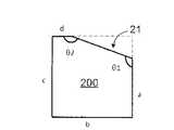
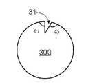
図1A、1B、2A、2B、3Aおよび3Bは、いくつかの実施形態によるマイクロフレーク100、200および300を示す概略図である。マイクロフレーク100、200および300のそれぞれは、エッジに存在する第1のタイプのノッチ(それぞれ11、21および31)のみを有する。図1A、2A、および3Aはそれぞれのマイクロフレーク100、200および300の上面を示し、図1B、2Bおよび3Bは、それぞれのマイクロフレーク100、200、および300の下面を示す。 1A, 1B, 2A, 2B, 3A and 3B are
「上面」および「下面」という用語は、本明細書ではマイクロフレークの2つの対向する表面を指すために使用されることに留意されたい。使用中(例えば多重アッセイプロセス中)、下面は上部にあってもよく、一方、上面はマイクロフレークの下部にあってもよく、またはその逆であってもよい。 It should be noted that the terms "top" and "bottom" are used herein to refer to two opposing surfaces of microflakes. During use (eg, during a multiplex assay process), the bottom surface may be at the top, while the top surface may be at the bottom of the microflakes, or vice versa.
本明細書の実施例はマイクロフレークがその基本形状として任意の形状、例えば多角形、円形などであり得ることを示す。なおマイクロフレークのベース形状とはノッチのないマイクロフレークの形状をいう。 The examples herein show that the microflakes can have any shape as their basic shape, such as polygons, circles, and the like. The base shape of the microflake means the shape of the microflake without a notch.
第1のタイプのノッチ11、21および31はそれぞれのマイクロフレーク100、200および300の向き(例えば前面または背面、上面または下面)を画定する。検出器は例えば第1のタイプのノッチの2つの隣接する辺の長さまたは2つの隣接する角度を識別することによって、マイクロフレークの観察された表面がマイクロフレークの上面であるか下面であるかを識別することができる。検出器がマイクロフレークのどの表面が観察されつつあるか、または観察されたかを識別した後、検出器または別のデバイスは次にマイクロフレークのエッジにおけるコードが読み取られるべき方向を決定することができる。 The first type of
図1Aは第1のタイプのノッチ11が角の三角形部分(点線で示される)を除去することによって形成され得ることをさらに示す。第1のタイプのノッチ11を画定するエッジアウトラインの部分は、直線(図1Aに示される)、曲線、または別の形状の線であってもよい。図1Aおよび図1Bに示されるように、第1のタイプのノッチ11はその2つの隣接する辺(例えば「a」および「d」)と非対称の関係を形成し、ここで、aおよびdは異なる長さ(例えばa < d)を有する。隣接する辺の長さのこの差は、検出器がマイクロフレークの観察された表面がマイクロフレークの上面であるか、または下面であるかを決定するのに役立つ。例えば識別子はマイクロフレークの第2のタイプのノッチおよび/またはエッジセグメントのシーケンスの形態でコード化されてもよい。マイクロフレークの上面から時計回りに読み取られるシーケンスは、マイクロフレークの下面から時計回りに読み取られるシーケンスとは異なることがある。検出されたシーケンスを正確に読み取り解釈するために、検出器は最初に第1のタイプのノッチを使用してマイクロフレークの表面を識別する。図1Aおよび図1Bの例では検出器が第1のタイプのノッチから時計回りに辺の長さを読み取ることによって、観察された表面が上面であるか下面であるかを識別することができる。すなわち長さをa →b →c →dと読むと観察面は上面となる。しかし長さをd →c →b →aと読むと観察される表面は下面である。一実施形態では、検出器がマイクロフレークのどちらの面が観察されつつあるか、または観察されているかを判定するために、所定の方向(例えば時計回り)に沿うことによって、第1のタイプのノッチの2つの隣接する辺の長さを比較することができる。時計回り方向に読み取る場合、第1の遭遇した隣接辺(例えばa)が第2の遭遇した隣接辺(例えばd)より短い場合、図1Aの例によれば観察された表面は上面である。同様に時計回り方向に読み取る場合、第1の遭遇した隣接辺(例えばd)が第2の遭遇した隣接辺(例えばa)よりも長い場合、図1Bの例によれば観察された表面は下面である。 FIG. 1A further shows that the first type of
代替的にまたは追加的に、第1のタイプのノッチ11はその2つの隣り合う角度(例えばθ1およびθ2)と非対称な関係を形成することができ、θ1およびθ2は異なった値(例えばθ1 > θ2)を有する。各隣接する角度は第1のタイプのノッチ11の辺面と、マイクロフレーク100の1つの隣接する辺面とによって画定される。隣接する角度のこの差は検出器がマイクロフレークの観察された表面がマイクロフレークの上面であるか、または下面であるかを決定するのに役立つ。例えば検出器は第1のタイプのノッチ11から時計回りに読み取られた第1の遭遇角度がθ1である場合、または第1のタイプのノッチ11から時計回りに読み取られた2つの隣接角度がθ1 → θ2である場合、または第1のタイプのノッチ11から時計回りに読み取られた2つの隣接角度がより大きい角度(例えばθ1)であり、続いてより小さい角度(例えばθ2)である場合に、観察された表面を上面であると判定することができる。マイクロフレーク100の下面に関しても同様の測定を行うことができる。Alternatively or additionally, the first type of
図2Aはマイクロフレーク200の角から非二等辺三角形部分を除去することによって、第1のタイプのノッチ21を形成することができることを示す(点線で示す)。図2Aおよび図2Bに示されるように、第1のタイプのノッチ21はその2つの隣接する辺(例えば「a」および「d」)と非対称の関係を形成し、ここでaおよびdは異なる長さ(例えば「a>d」)を有する。代替的にまたは追加的に第1のタイプのノッチ21はその2つの隣り合う角度(例えばθ1およびθ2)と非対称な関係を形成することができ、ここでθ1およびθ2は異なった値(例えばθ1 < θ2)を有する。隣接する辺の長さおよび/または隣接する角度のこの差は検出器がマイクロフレークの観察された表面がマイクロフレーク200の上面であるか、または下面であるかを決定するのに役立つ。FIG. 2A shows that the first type of
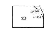
図3Aは第1のタイプのノッチ31がマイクロフレーク300からくさび部分を除去することによって形成され得ることを示す(点線で示される)。図3Aおよび図3Bに示されるように、第1のタイプのノッチ31はその2つの隣り合う角度(例えばθ1およびθ2)と非対称の関係を形成し、θ1およびθ2は異なった値(例えばθ1 < θ2)を有する。第1のタイプのノッチ31は、第1のタイプのノッチ31を形成するウェッジ部分の2つの辺部と非対称の関係を形成することもできる。隣接する角度および/または辺面の長さのこの差は、検出器がマイクロフレークの観察された表面がマイクロフレーク300の上面であるか、または下面であるかを決定するのに役立つ。FIG. 3A shows that the first type of
図4〜7はいくつかの実施形態によるコード化されたマイクロフレークの上面図を示す。マイクロフレークのコードはマイクロフレークのエッジにおける第2のタイプのノッチの有無によって表される1と0の2進シーケンスである。説明を簡単にするために以下の例では第2のタイプのノッチの存在が2進値「1」を示し、第2のタイプのノッチの不在が2進値「0」を示すと仮定する。存在しない第2のタイプのノッチは同じ位置に存在するエッジセグメントと同等である。代替実施形態では「1」および「0」の表現を逆にすることができることを理解されたい。第2のタイプのノッチは第1のタイプのノッチの形状と異なる限り、任意の形状であり得る。 Figures 4-7 show top views of the coded microflakes according to some embodiments. The microflake code is a binary sequence of 1s and 0s represented by the presence or absence of a second type of notch at the edge of the microflake. For simplicity, the following example assumes that the presence of a second type notch indicates a binary value of "1" and the absence of a second type of notch indicates a binary value of "0". A second type of notch that does not exist is equivalent to an edge segment that exists in the same position. It should be understood that in alternative embodiments the expressions "1" and "0" can be reversed. The second type notch can have any shape as long as it differs from the shape of the first type notch.
一実施形態では、検出器が以下のようにマイクロフレークのコードを読み取ることができる。第1のタイプのノッチから開始して検出器は第2のタイプのノッチが存在するか存在しないかを識別するために、固定された物理的距離の間隔(例えば単位長さX)でマイクロフレークのエッジアウトラインをチェックすることができる。検出器は観察された表面が上面であるか下面であるかに基づいて、第1のタイプのノッチの一端から所定の方向(例えば時計回りまたは反時計回り)に所定の距離でコードの読み取りを開始することができる。例えばコード(最下位ビット(LSB)から最上位ビット(MSB)まで)は、マイクロフレークの上面から時計回りに読み取られるビットシーケンスであると定義されてもよい。代替の定義を使用することもできる。 In one embodiment, the detector can read the code for the microflakes as follows: Starting with the first type of notch, the detector uses microflakes at fixed physical distance intervals (eg unit length X) to identify the presence or absence of the second type of notch. You can check the edge outline of. The detector reads the code at a given distance in a given direction (eg, clockwise or counterclockwise) from one end of the first type of notch, based on whether the observed surface is top or bottom. You can start. For example, the code (from least significant bit (LSB) to most significant bit (MSB)) may be defined as a bit sequence read clockwise from the top of the microflakes. Alternative definitions can also be used.
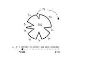
図4は一実施形態によるコード化マイクロフレーク400の上面図を示す。この例では最下位ビットから最上位ビットへのコードがこの平面図において、第1のタイプのノッチ41から点線矢印45の方向に時計回りに読み出される。この例における各第2のタイプのノッチの形状はその2つの実質的に平行な辺面(図示を簡単にするために、第2のタイプのノッチのうちの1つのみが42で示されている)と、2つの実質的に平行な辺面に隣接する下面とによって画定される。第1のタイプのノッチも第2のタイプのノッチも存在しないエッジアウトラインの部分はエッジセグメントと呼ばれる(図示を簡略化するためにエッジセグメントのうちの1つだけにコード43が付されている)。マイクロフレーク400の上面図は、エッジセグメント、第1のタイプのノッチの辺面、および第2のタイプのノッチの辺面の組み合わせであるエッジアウトラインを示す。この例では長さXの各エッジセグメントは「0」ビットとして解釈され、長さXの各第2のタイプのノッチは「1」ビットとして解釈される。第2のタイプのノッチの長さは「w」によって示されるその開口部の2つの辺を横切って測定される長さとして定義され得る(図を簡略化するために、1つのみがラベル付けされる)。2つの連続する第2のタイプのノッチは角、例えば上面図に示されるような左下の角を占めてもよい。読み出される順序(時計回り)で表されるマイクロフレーク400のエッジアウトラインは3X→(2X)→X→6X→(2X)→4X→(2X)→(2X)→X→(2X)→2X→(2X)→2X→4X→(2X)→2X→(2X)→Xであり、括弧内の値は対応する第2タイプのノッチの長さ(すなわち1つ以上の「1」を表す)を示す。したがって上記の長さのシーケンスはマイクロフレーク400を識別するデジタルコード(最下位ビットから最上位ビット)に、次のように解釈することができる:011001100000011001101111000011000000011000。 FIG. 4 shows a top view of the coded microflake 400 according to one embodiment. In this example, the least significant bit to most significant bit code is read clockwise from the
図5は別の実施形態によるコード化マイクロフレーク500の上面図を示す。この例では最下位ビットから最上位ビットへのコードがこの平面図において第1のタイプのノッチ51から点線矢印55の方向に時計回りに読み出される。この例の各第2のタイプのノッチは1つの端で結合する2つの辺面によって定義されている(図を単純化するために、第2のタイプのノッチの1つだけが52とラベル付けされている)。上面図から各第2のタイプのノッチは三角形の形状を有する。マイクロフレーク500のエッジアウトラインは図4のマイクロフレーク400のエッジアウトラインと同様に読み取られ、デジタルコードに解釈され得る。 FIG. 5 shows a top view of the coded microflake 500 according to another embodiment. In this example, the least significant bit to most significant bit code is read clockwise from the
図6および図7はいくつかの他の実施形態によるコード化されたマイクロフレーク600およびコード化されたマイクロフレーク700の上面図をそれぞれ示す。マイクロフレーク600および700はそれぞれ第1のタイプのノッチ61および71を有する。マイクロフレーク600および700に関連するコードはマイクロフレーク400および500に関連する前述の説明に従って読み取られ、それぞれのデジタルコードに解釈され得る。 6 and 7 show top views of the coded microflake 600 and the coded microflake 700 according to some other embodiments, respectively. The
図4〜7に示される第2のタイプのノッチは対称的な形状を有する。代替の実施形態では、第2のタイプのノッチが非対称形状を有してもよく、例えば一方の辺が他方の辺よりも長い。第2のタイプのノッチは第1のタイプのノッチの形状と区別可能である限り、任意の形状を有することができる。 The second type of notches shown in FIGS. 4-7 have a symmetrical shape. In an alternative embodiment, the second type of notch may have an asymmetrical shape, eg, one side is longer than the other. The second type notch can have any shape as long as it is distinguishable from the shape of the first type notch.
一実施形態では、第2のタイプのノッチの開口部は任意の長さ(その開口部の2つの辺を横切って測定される)であり、所定の単位長さの整数倍(例えば図4〜7においてXで示される)であり得る。いくつかの実施形態では、第2のタイプのノッチの開口の長さは2進シーケンスにおいて第1の2進値を有する連続ビットの数(すなわちデジタルコード)を定義し、各エッジセグメントの長さは2進シーケンスにおいて第2の2進値を有する連続ビットの数を定義する。いくつかの実施形態では、第2のタイプのノッチの長さは所定の長さ、例えば1または2の単位長さに制限される。例えばマイクロフレークは1の長いシーケンスを表すために、連続した単位長さの第2のタイプのノッチのシーケンスを含むことができる。 In one embodiment, the opening of the second type of notch is of arbitrary length (measured across two sides of the opening) and is an integral multiple of a given unit length (eg, FIGS. 4–4). (Represented by X in 7). In some embodiments, the length of the opening of the second type of notch defines the number of consecutive bits (ie, the digital code) that have the first binary value in the binary sequence, and the length of each edge segment. Defines the number of consecutive bits that have a second binary value in a binary sequence. In some embodiments, the length of the second type of notch is limited to a predetermined length, for example one or two unit lengths. For example, microflakes can include a second type of notch sequence of consecutive unit lengths to represent a long sequence of ones.
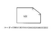
図8Aおよび8Bはいくつかの実施形態による2つのコード化されたマイクロフレーク810および820の各々の上面図を示す。マイクロフレーク810および820の各々は、上面図において上部右角に第1のタイプのノッチを有する。マイクロフレーク810は連続した単位長さの第2のタイプのノッチのシーケンスを使用したシーケンスでコード化される。図8Aの例では第2のタイプのノッチが角領域の近傍を避けて、エッジアウトラインの所定の部分(例えばP1、P2、P3およびP4)内に形成される。第2のタイプのノッチの一方の辺(コードの最上位ビットまたは最下位ビットを表す)は第1のタイプのノッチの辺に隣接することができる。マイクロフレーク820はいかなる第2のタイプのノッチも有さず、シーケンス0でコード化される。 8A and 8B show top views of each of the two coded
図8Cおよび8Dはいくつかの実施形態による、2つのコード化されたマイクロフレーク830および840の各々の上面図を示す。マイクロフレーク830および840の各々は上面図の上部右角に第1のタイプのノッチを有する。マイクロフレーク830および840の各々は第2のタイプのノッチおよびエッジセグメントのシーケンスを用いて1と0の交互のシーケンスでコード化される。これらの例では図8Cおよび8Dに示すように、マイクロフレーク830および840に関連するコード(最下位ビットから最上位ビットへ)はそれぞれの第1のタイプのノッチから時計回りに読み取られ、解釈される。 8C and 8D show top views of each of the two coded
図8Cおよび8Dはさらにマイクロフレーク830および840のエッジアウトラインを取り囲む所定の位置を示す。コードのビット0〜29の所定の位置は点線でマークされている。これらの実施形態では、ビットがその所定の位置が第2のタイプのノッチを有さない場合には第1の値を有し、その所定の位置が第2のタイプのノッチの存在を有する場合には第2の値を有する。検出器はコードのビット値を決定する際に間隔を測定しないので、隣接する所定の位置間の間隔は任意の値であってもよい。コードを読み取るとき検出器にはこれらの所定の位置のマーキングを有する検出テンプレートを設けることができる。検出テンプレートは第2のタイプのノッチがこれらの位置に存在するかどうかを決定するために、検出器のためのマイクロフレークのエッジアウトラインの画像上に描かれてもよい。検出テンプレートはマイクロフレークの基本形状と同じ形状を有することができ、ビットのための位置マーキングを有する。検出テンプレートの例は、図8Cおよび8Dの位置マーキングを有する点線の長方形880および890であってもよい。検出テンプレートはその位置マーキングがビット位置を示す限り、マイクロフレークの基本形状よりも大きくても、小さくてもまたは同じサイズであってもよい。 Figures 8C and 8D also show predetermined locations surrounding the edge outlines of the
一実施形態では、マイクロフレークがそのエッジセグメントおよび第2のタイプのノッチによって形成される2進シーケンスに加えてグループ識別子によって識別されてもよい。グループ識別子は図8A〜8Dに示されるθ1およびθ2のような第1のタイプのノッチの隣接する角度の組合せによってコード化することができる。説明を容易にするために図9A、図9Bおよび図9Cは第2のタイプのノッチのない3つのグループの例を示す。グループ識別子はマイクロフレークのデジタルコードを形成するために、本明細書に記載される2進シーケンスのいずれかと組み合わせることができることが理解される。In one embodiment, microflakes may be identified by a group identifier in addition to the binary sequence formed by their edge segments and second type notches. Group identifiers can be encoded by a combination of adjacent angles of the first type of notches, suchas θ 1 and θ2 shown in Figures 8A-8D. For ease of explanation, FIGS. 9A, 9B and 9C show examples of the second type of three unnotched groups. It is understood that the group identifier can be combined with any of the binary sequences described herein to form the digital code for the microflakes.
図9Aは2つの隣り合う角度が同じ値(例えばθ1=θ2=135°)を有するグループ識別子の第1の例を示す。これは非対称な辺(例えば長方形)を有するマイクロフレークに適用可能である。図9Bは例えばθ1=150°, θ2=120°であるグループ識別子の第2の例を示す。図9Cは例えばθ1=120°, θ2=150°のようなグループ識別子の第3の例を示す。一実施形態では、角度差 =(θ1-θ2)の異なる値が異なるグループ識別子に対応する。一実施形態では角度差の値がビット数によって表すことができ、この数はグループの数に従って決定される。FIG. 9A shows a first example of a group identifier in which two adjacent angles have the same value (
図10Aおよび10Bは一実施形態による、マイクロフレーク1000の3次元(3D)図および断面図の各々を示す。図10Bのマイクロフレーク1000の断面図は上面1010と、上面1010に実質的に平行な下面1020と、上面1010および下面1020を取り囲むエッジ1030(すなわち周辺部)とを示す。上面1010および下面1020は実質的に平坦であり、例えば図示のようにX―Y軸(すなわちX―Y平面)によって張られる水平面に実質的に平行である。エッジ1030は2つの表面1010および1020に対して実質的に垂直であり、例えば図示のようにZ軸に対して実質的に平行である。図10Bに示すようにエッジ1030は上面1010と下面1020との間に垂直に延びる。一実施形態では、上面1010および下面1020がX―Y平面に対して対称であってもよい。多重アッセイにおいて使用される場合、表面1010および1020の一方または両方は標的分析物と結合するための試料(例えばプローブ)に結合され得る。 10A and 10B show a three-dimensional (3D) view and a cross-sectional view of the
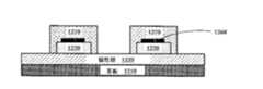
一実施形態では、マイクロフレーク1000が実質的に透明な磁性ポリマー材料から作製される。磁性ポリマー材料は磁性金属粒子をポリマーに混合することによって製造することができる。磁気応答性であるマイクロフレーク1000は多重アッセイのプロセスの間の磁場で容易に操作され得、そして取り扱われ得る。 In one embodiment, the
図10Cは一実施形態によるマイクロフレーク1000のエッジアウトライン1080を示す。エッジアウトライン1080は前述のエッジコード化スキームのいずれか1つに従ってマイクロフレーク1000をコード化する。図10Cはエッジアウトライン1080が平面(例えばこの例ではX―Y平面)上の上面1010および下面1020の両方の周辺の輪郭を描くことを示す。この平面は上面1010および下面1020に実質的に平行である。したがって検出器は表面1010および1020の両方からマイクロフレーク1000の同じコードを検出することができる。コードの同一の2進シーケンスは表面1010および1020の一方から時計回りに、表面1010および1020の他方から反時計回りに読み取ることができる。 FIG. 10C shows the
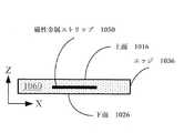
図10Cおよび図10Dは別の実施形態によるマイクロフレーク1060の3D図および断面図の各々を示す。図10Aおよび10Bのマイクロフレーク1000と同様にマイクロフレーク1060はまた上面1016と、上面1016に実質的に平行な下面1026と、上面1016および下面1026を取り囲むエッジ1036とを含む。またマイクロフレーク1060には例えばニッケル、コバルト、鉄などの磁性金属ストリップ1050が埋め込まれている。磁性金属ストリップ1050はマイクロフレーク1060内に埋め込まれた非透過(すなわち不透明)層である。磁性金属ストリップ1050はマイクロフレーク1060の上部透明ポリマー層と下部透明ポリマー層との間に挟まれてもよい。一実施形態では、磁性金属ストリップ1050がマイクロフレーク1060の幾何学的中心に配置される。幾何学的中心位置はマイクロフレーク1060が多重アッセイプロセス中に磁場で拾い上げられるか、または収集されるときにマイクロフレーク1060上のトルクを低減するのに役立つ。図10Aのマイクロフレーク1000と同様に、マイクロフレーク1060は上面1016および下面1026に実質的に平行な平面上で、上面1016および下面1026の両方の周囲の輪郭を描くエッジアウトラインによってコード化される。 10C and 10D show 3D and cross-sectional views of the
図10Eは一実施形態によるマイクロフレーク1000または1060のエッジアウトライン1080を示す。エッジアウトライン1080は前述のエッジコード化スキームのいずれか1つに従ってマイクロフレーク1000をコード化する。一例としてマイクロフレーク1000を使用すると、図10Eはエッジアウトライン1080が平面(例えばこの例ではX―Y平面)上の上面1010および下面1020の両方の周辺部(すなわちエッジ)の輪郭を描くことを示す。この平面は上面1010および下面1020に実質的に平行である。従って検出器は表面1010および1020のいずれか1つから、マイクロフレーク1000の同一コードを検出することができる。コードの同一の2進シーケンスは表面1010および1020の一方の面から時計回りに、表面1010および1020の他方の面から反時計回りに読み取ることができる。 FIG. 10E shows an
前述のマイクロフレークは半導体製造および/または微小電気機械システム(MEMS)製造のために開発された技術に基づいて製造することができる。例えば以下に記載されるマイクロフレーク製造では、半導体および/または微小電気機械システム製造の当業者の技術分野で知られている基板材料、犠牲材料、およびフォトレジスト材料を使用する。半導体および/または微小電気機械システム製造分野の当業者に知られている多くの工程は図示を簡略化するために以下では省略される。例えば省略された工程は後続の処理のために表面を準備するための表面洗浄、溶媒を除去するためのソフトベーキングなどを含むことができる。以下に記載される製造プロセスは従来のマイクロキャリアを製造するためのプロセスと比較してより単純であり、低コストで、より多くの反応領域を確保する。 The aforementioned microflakes can be manufactured based on techniques developed for semiconductor manufacturing and / or microelectromechanical systems (MEMS) manufacturing. For example, the microflake manufacturing described below uses substrate materials, sacrificial materials, and photoresist materials known in the art of semiconductor and / or microelectromechanical system manufacturing. Many steps known to those skilled in the art of semiconductor and / or microelectromechanical system manufacturing are omitted below for the sake of brevity. For example, the omitted steps can include surface cleaning to prepare the surface for subsequent processing, soft baking to remove the solvent, and the like. The manufacturing process described below is simpler than the process for manufacturing conventional microcarriers, at a lower cost, and secures more reaction regions.
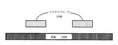
図11A、図11B、図11Cおよび図11Dは第1の実施形態によるマイクロフレークを製造する工程を示す。図14は第1の実施形態によるマイクロフレークを製造するための方法1400を示す流れ図である。第1の実施形態に従って製造されたマイクロフレークの例としては図10Aおよび10Bのマイクロフレーク1000が挙げられるが、これらに限定されない。図11A〜図11Dおよび図14を参照すると方法1400はウェーハ上の実質的に平坦な基板1110の上に犠牲層1120を堆積させる工程1410から開始する。続いて工程1420において磁気フォトレジスト層1130(例えば磁気ポリマー層)が犠牲層1120の上に堆積される。いくつかの実施形態では、磁気フォトレジスト層1130は実質的に透明であってもよく、または少なくとも部分的に透明であってもよい。工程1430において、マイクロフレークパターンを含むマスク層1140を使用して、磁気フォトレジスト層1130をマイクロフレークにパターン化する。マスク層1140は磁気フォトレジスト層1130の領域を紫外線(UV)光に選択的に露光し、それによって個々のマイクロフレーク1100を画定する。各マイクロフレーク1100は上面および下面に実質的に平行な平面上でマイクロフレーク1100の上面および下面の両方の2D周辺部の輪郭を描くエッジアウトラインによってコード化される。一実施形態では、マスク層1140がウェーハ上に異なるコードでコード化されたマイクロフレークを画定することができる。したがって異なるコードを有するマイクロフレークを同じウェーハ上に同時に製造することができる。工程1440において犠牲層1120は基板1110からマイクロフレーク1100を剥離するためにエッチングされるか、さもなければ除去される。 11A, 11B, 11C and 11D show the steps of producing microflakes according to the first embodiment. FIG. 14 is a flow chart showing a
図12A〜12Iは第2の実施形態によるマイクロフレークを製造する工程を示す。図15は第2の実施形態によるマイクロフレークを製造するための方法1500を示す流れ図である。第2の実施形態に従って製造されたマイクロフレークの例としては図10Cおよび10Dのマイクロフレーク1060が挙げられるが、これらに限定されない。図12A、図12Bおよび図15を参照すると、方法1500はウェーハ上の実質的に平坦な基板1210の上に犠牲層1220を堆積させる工程1510から開始する。続いて工程1520において、フォトレジスト層1230a(例えばポリマー層)が犠牲層1220の上に堆積される。フォトレジスト層1230aはいくつかの実施形態では実質的に透明であってもよく、または少なくとも部分的に透明であってもよい。工程1530でマイクロフレークパターンを含むマスク層1240を使用してフォトレジスト層1230aを複数のブロック1230にパターン形成し各ブロック1230は対応するマイクロフレークの一部となる。マスク層1240はフォトレジスト層1230aの領域をUV光に選択的に露光し、それによって個々のブロック1230を画定する。 12A-12I show the steps of producing microflakes according to the second embodiment. FIG. 15 is a flow chart showing a
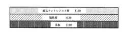
リフトオフプロセスを実行して各下部上に磁性金属層を堆積させることができる。図12C〜12Fは一実施形態によるリフトオフプロセスを示す。第2の犠牲材料1250は残りの構造の上にブランケット堆積される。第2の犠牲材料1250はブロック1230の各々の上面の少なくとも一部を露出するようにパターン化される。物理気相成長法(PVD)、化学気相成長法(CVD)などによって、磁性金属1260の薄層をパターン化された犠牲材料1250および露出したブロック1230の上部全体を覆うように堆積させる。次いで第2の犠牲材料1250は、例えば化学溶液または代替手段を使用することによって剥離される。したがって工程1540において磁性金属層1260のストリップがブロック1230の各々の上面の少なくとも一部の上に形成される。 A lift-off process can be performed to deposit a magnetic metal layer on each bottom. Figures 12C-12F show the lift-off process according to one embodiment. The second
図12G〜12Iおよび図15を参照すると、工程1550において残りの構造の上、すなわちブロック1230の上および各ブロック1230の上の磁性金属層1260の上に、別のフォトレジスト層1270a(例えばポリマー層)がブランケット堆積される。一実施形態では、フォトレジスト層1270aがフォトレジスト層1230aと同じ材料であることができる。フォトレジスト層1270aはいくつかの実施形態では実質的に透明であってもよく、または少なくとも部分的に透明であってもよい。工程1560ではマイクロフレークパターンを含むマスク層1280を使用して、フォトレジスト層1270aをマイクロフレーク1200にパターン化する。各マイクロフレーク1200は上面および下面に実質的に平行な平面上でマイクロフレーク1200の上面および下面の両方の2D周辺部の輪郭を描くエッジアウトラインによってコード化される。一実施形態では、マスク層1280がウェーハ上に異なるコードでコード化されたマイクロフレークを画定することができる。したがって異なるコードを有するマイクロフレークを、同じウェーハ上に同時に製造することができる。工程1570において犠牲層1220は基板1210からマイクロフレーク1200を剥離するためにエッチングされるか、さもなければ除去される。 With reference to FIGS. 12G-12I and FIG. 15, another
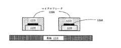
図13は一実施形態による、基板1350上に複数のマイクロフレークを有する半導体ウェーハ1300を示す概略図である。図13の例は、例えば異なるコードに対応する異なるエッジアウトラインを画定するマスク層でマイクロフレークをパターン化することによって、同一のウェーハ上に異なるコードを有するマイクロフレークが製造され得ることを示す。パターン化工程の非限定的な例は図14の工程1430および図15の工程1560で提供されている。例えばウェーハ1300はマイクロフレーク810、820、830および840(図8A〜図8D)を含むように製造されてもよい。一実施形態ではウェーハ1300が複数の仕切りを含むことができ、各仕切りは同じコードのマイクロフレークのグループを含む。代替の実施形態では、ウェーハが図13に示すものよりも多くの異なるコード、または少ない異なるコードを有するマイクロフレークを含むことができることを理解されたい。 FIG. 13 is a schematic view showing a semiconductor wafer 1300 having a plurality of microflakes on the substrate 1350 according to one embodiment. The example of FIG. 13 shows that microflakes with different codes can be produced on the same wafer, for example by patterning the microflakes with mask layers that define different edge outlines corresponding to different codes. Non-limiting examples of patterning steps are provided in
前述のマイクロフレークは多重アッセイキットを含むがこれに限定されない多くの用途を有することができる。多重アッセイキットは少なくとも第1の標的分析物への標的特定結合を形成するための上記実施形態のいずれかによる第1のマイクロフレークと、第1の標的分析物とは異なる第2の標的分析物への標的特定結合を形成するための上記実施形態のいずれかによる第2のマイクロフレークとを含む。第1のマイクロフレークは第1の2進シーケンスによって識別され、第2のマイクロフレークは第2の2進シーケンスによって識別される。第1の2進シーケンスは第1のマイクロフレークの上面および下面に実質的に平行な第1の平面上の第1のマイクロフレークの周囲の輪郭を描く第1のエッジアウトラインによってコード化される。第2の2進シーケンスは第2のマイクロフレークの上面および下面に実質的に平行な第2の平面上の第2のマイクロフレークの周囲の輪郭を描く第2のエッジアウトラインによってコード化される。 The microflakes described above can have many uses, including but not limited to multiple assay kits. The multiplex assay kit comprises a first microflake according to any of the above embodiments for forming a target specific bond to at least the first target analyte and a second target analyte different from the first target analyte. Includes a second microflake according to any of the above embodiments for forming a target specific bond to. The first microflake is identified by the first binary sequence and the second microflake is identified by the second binary sequence. The first binary sequence is encoded by a first edge outline that outlines the perimeter of the first microflake on a first plane that is substantially parallel to the top and bottom surfaces of the first microflake. The second binary sequence is encoded by a second edge outline that outlines the perimeter of the second microflake on a second plane that is substantially parallel to the top and bottom surfaces of the second microflake.
図16は一実施形態による、デジタル的にコード化された磁気マイクロフレークを復号するための方法1600を示す流れ図である。方法1600は図17に関連して説明される機械などの検出器によって実行されてもよい。方法1600は検出器が複数の照射されたマイクロフレークを含む画像を取得する工程1610から開始する。工程1620において検出器は照射された各マイクロフレークのエッジアウトラインを検出する。工程1630において、検出器はエッジアウトラインから対応するマイクロフレークの配向を決定するために第1のタイプのノッチを識別する。工程1640において検出器は第2のタイプのノッチの存在(または不在)を検出して、エッジアウトラインを2進シーケンスに復号する。2進シーケンスは対応するマイクロフレークを識別するデジタルコードである。 FIG. 16 is a flow chart showing a
図17は一実施形態による、コード化されたマイクロフレークを復号するためのソフトウェア製品1780を実行するように動作可能な機械1700を示す図である。ソフトウェア製品1780は機械可読媒体(コンピュータ可読媒体とも呼ばれる非一時的機械可読記憶媒体1720、プロセッサ可読媒体、またはコンピュータ可読プログラムコードが組み込まれたコンピュータ使用可能媒体など)に格納され得る。非一時的機械可読媒体1720は磁気、光学、またはディスケット、コンパクトディスク読取り専用メモリ(CD-ROM)、デジタル多用途ディスク読取り専用メモリ(DVD-ROM)を含む電気記憶媒体、ハードドライブまたはソリッドステートドライブなどのメモリデバイス(揮発性または不揮発性)または別の記憶機構を含む任意の適切な有形的表現媒体とすることができる。機械可読媒体1720は命令、コードシーケンス、構成情報、または他のデータの様々なセットを含むことができ、これらは実行されるとプロセッサ1710に、例えば図16の方法1600に従って画像1750内のコード化されたマイクロフレークを復号させる。画像1750は機械1700のI/Oデバイス1730によって取得され得る。画像1750から機械1700はマイクロフレークに関連する少なくとも識別されたコードを含む出力を生じることができる。当業者は説明された実施形態を実施するために必要な他の命令および動作もまた、機械可読媒体1720上に格納され得ることを理解するであろう。機械可読媒体から実行されるソフトウェアは説明されたタスクを実行するために回路とインターフェースで接続することができる。 FIG. 17 is a diagram illustrating a
本発明をいくつかの実施形態に関して説明してきたが、当業者は本発明が説明した実施形態に限定されず、添付の特許請求の範囲の精神および範囲内で修正および変更を加えて実施できることを理解するであろう。本願の記載はよって限定するものでなく例証するものとしてみなすこととする。 Although the present invention has been described with respect to some embodiments, those skilled in the art are not limited to the embodiments described by the present invention, and can be modified and modified within the spirit and scope of the appended claims. You will understand. The description of the present application is not limited thereto, but is regarded as an example.
Claims (18)
Translated fromJapanese上面および上面に平行な下面とを有し、上面および下面のうちの少なくとも1つが標的分析物と結合するための標的特定プローブに結合されるポリマー層を含み、
ここで、マイクロフレークは上面および下面に平行な平面上のエッジアウトラインによってコード化された2進シーケンスのビットによって識別され、
ここで、2進シーケンス中のビットはエッジアウトラインを取り囲むそれぞれの所定の位置でコード化され、
前記エッジアウトラインが、前記2進シーケンスを読み取る開始点と方向を示す第1のタイプのノッチを含み、
マイクロフレークは、第1のタイプのノッチの隣接する角度によってコード化されるグループ識別子によってさらに識別され、隣接する角度の異なる組み合わせが異なるグループ識別子をコード化する2進シーケンスでコード化されたマイクロフレーク。Microflakes encoded in a binary sequence
And aflat line lower surfaceto the upper surface and the upper surface, at least one of the upper and lower surfacescomprises a polymer layer bonded to a target specific probe for binding the target analyte,
Here, the micro flakes are identified by a bit of the coded binary sequence by the edge outline of theflat line planeon the upper and lower surfaces,
Here, the bits in the binary sequence are coded at their respective predetermined positions surrounding the edge outline.
The edge outline includes a first type notch indicating the starting point and direction to read the binary sequence.
Microflakes are further identified by a group identifier encoded by the adjacent angles of the first type of notch, and microflakes encoded in a binary sequence in which different combinations of adjacent angles encode different group identifiers. ..
第1の標的分析物に標的特定結合を形成する第1のマイクロフレークと、
第1の標的分析物とは異なる標的分析物に標的特定結合を形成する第2のマイクロフレークと、
第1のマイクロフレークは第1の2進シーケンスによって識別され、第2のマイクロフレークは第1とは異なる第2の2進シーケンスによって識別され、
第1の2進シーケンスは第1のマイクロフレークの上面および下面に平行な第1の平面上の第1のエッジアウトラインによってコード化され、第1の2進シーケンス内のビットは第1のエッジアウトラインを囲むそれぞれの所定の位置でコード化され、
第2の2進シーケンスは第2のマイクロフレークの上面および下面に平行な第2の平面上の第2のエッジアウトラインによってコード化され、第2の2進シーケンス内のビットは第2のエッジアウトラインを囲むそれぞれの所定の位置でコード化されるマイクロフレークを含み、
第1のエッジアウトラインおよび第2のエッジアウトラインのそれぞれが、2進シーケンスを読み取る開始点と方向を示す第1のタイプのノッチを含み、
第1のマイクロフレークと第2のマイクロフレークのそれぞれが、第1のタイプのノッチの隣接する角度によってコード化されるグループ識別子によってさらに識別され、隣接する角度の異なる組み合わせが異なるグループ識別子をコード化する多重アッセイのための装置。A device for multiple assays
A first microflake that forms a target-specific bond to the first target analyte,
A second microflake that forms a target specific bond on a target analyte different from the first target analyte,
The first microflake is identified by a first binary sequence and the second microflake is identified by a second binary sequence different from the first.
The first binary sequence is encoded by a first edge outline on aflat line of the first planeon the upper and lower surface of the first micro-flakes, bits within a first binary sequence a first edge Encoded in each given position around the outline,
Second binary sequence is coded by a second edge outline on aflat line of the second planeon the upper and lower surface of the second micro-flakes, bits of the second binary sequence and the second edgelook including the micro flakes are encoded in respective predetermined positions surrounding theoutline,
Each of the first edge outline and the second edge outline contains a first type of notch indicating the starting point and direction to read the binary sequence.
Each of the first and second microflakes is further identified by a group identifier encoded by the adjacent angles of the first type of notch, and different combinations of adjacent angles encode different group identifiers. A device for multiple assays.
基板は;
基板上の複数の第1のマイクロフレークであって、各第1のマイクロフレークは第1の2進シーケンスによって識別され、
基板上の複数の第2のマイクロフレークであって、各第2のマイクロフレークは第1の2進シーケンスとは異なる第2の2進シーケンスによって識別され、
各第1のマイクロフレークは基板に平行な平面上の第1のエッジアウトラインによってコード化された第1の2進シーケンスによって識別され、第1の2進シーケンス内のビットは第1のエッジアウトラインを囲むそれぞれの所定の位置でコード化され、
各第2のマイクロフレークは平面上の第2のエッジアウトラインによってコード化された第2の2進シーケンスによって識別され、第2の2進シーケンス内のビットは第2のエッジアウトラインを囲むそれぞれの所定の位置でコード化され、
第1のエッジアウトラインおよび第2のエッジアウトラインのそれぞれが、2進シーケンスを読み取る開始点と方向を示す第1のタイプのノッチを含み、
第1のマイクロフレークと第2のマイクロフレークのそれぞれが、第1のタイプのノッチの隣接する角度によってコード化されるグループ識別子によってさらに識別され、隣接する角度の異なる組み合わせが異なるグループ識別子をコード化することを含む半導体ウェーハ。It is a semiconductor wafer
The board is;
A plurality of first microflakes on the substrate, each first microflake being identified by a first binary sequence.
A plurality of second microflakes on the substrate, each of which is identified by a second binary sequence that is different from the first binary sequence.
Each first micro flakes are identified by the first binary sequence, which is encoded by a first edge outline on aflat line planeof the substrate, the bit of the first binary sequence a first edge outline Encoded in each predetermined position around
Each second microflake is identified by a second binary sequence encoded by a second edge outline on the plane, and the bits in the second binary sequence are each predetermined surrounding the second edge outline. It is encoded in theposition,
Each of the first edge outline and the second edge outline contains a first type of notch indicating the starting point and direction to read the binary sequence.
Each of the first and second microflakes is further identified by a group identifier encoded by the adjacent angles of the first type of notch, and different combinations of adjacent angles encode different group identifiers. Including semiconductor wafers.
Applications Claiming Priority (4)
| Application Number | Priority Date | Filing Date | Title |
|---|---|---|---|
| US201862776224P | 2018-12-06 | 2018-12-06 | |
| US62/776,224 | 2018-12-06 | ||
| US16/601,982 | 2019-10-15 | ||
| US16/601,982US11366109B2 (en) | 2018-12-06 | 2019-10-15 | Encoded microflakes |
Publications (2)
| Publication Number | Publication Date |
|---|---|
| JP2020118674A JP2020118674A (en) | 2020-08-06 |
| JP6920405B2true JP6920405B2 (en) | 2021-08-18 |
Family
ID=70970172
Family Applications (1)
| Application Number | Title | Priority Date | Filing Date |
|---|---|---|---|
| JP2019220042AActiveJP6920405B2 (en) | 2018-12-06 | 2019-12-05 | Coded microflakes |
Country Status (5)
| Country | Link |
|---|---|
| US (2) | US11366109B2 (en) |
| JP (1) | JP6920405B2 (en) |
| KR (1) | KR102299973B1 (en) |
| CN (1) | CN111286528A (en) |
| TW (1) | TWI721680B (en) |
Families Citing this family (3)
| Publication number | Priority date | Publication date | Assignee | Title |
|---|---|---|---|---|
| EP3916386B1 (en)* | 2019-01-23 | 2024-01-31 | BGI Shenzhen | Microbead |
| CN112149776B (en)* | 2020-09-30 | 2024-06-21 | 北京小龙潜行科技有限公司 | Visual tag and assembly thereof |
| CN116323906A (en)* | 2020-10-28 | 2023-06-23 | 深圳华大生命科学研究院 | Microbeads and preparation method thereof |
Family Cites Families (19)
| Publication number | Priority date | Publication date | Assignee | Title |
|---|---|---|---|---|
| US3405578A (en)* | 1965-04-07 | 1968-10-15 | Lkb Produkter Aktiebolag | Method for measuring the true cutting edge angle of a knife for a microtome |
| US20030203390A1 (en)* | 1995-10-26 | 2003-10-30 | Kaye Paul H. | Coded particles for process sequence tracking in combinatorial compound library preparation |
| JPH09320911A (en) | 1996-05-27 | 1997-12-12 | Mitsubishi Electric Corp | Semiconductor substrate with identification function |
| US6602602B1 (en) | 1999-04-26 | 2003-08-05 | Renssealer Polytechnic Institute | Epoxy-functional polymeric microbeads |
| US7008794B2 (en)* | 2000-03-22 | 2006-03-07 | Axela Biosensors Inc. | Method and apparatus for assay for multiple analytes |
| US8232092B2 (en)* | 2005-08-09 | 2012-07-31 | Maxwell Sensors, Inc. | Apparatus and method for digital magnetic beads analysis |
| EP2485052B1 (en)* | 2005-09-13 | 2015-05-06 | Affymetrix, Inc. | Encoded microparticles |
| EP2045601A1 (en) | 2007-03-26 | 2009-04-08 | Koninklijke Philips Electronics N.V. | Use of microcarrier beads for detection and/or isolation of cells by flow cytometry and/or dielectrophoresis |
| ES2729415T3 (en)* | 2008-12-23 | 2019-11-04 | Mycartis N V | Test device and method to perform biological tests |
| US20110007955A1 (en)* | 2009-07-08 | 2011-01-13 | Applied Biocode Inc. | Apparatus and Method for Barcoded Magnetic Beads Analysis |
| TW201211243A (en)* | 2010-06-17 | 2012-03-16 | Geneasys Pty Ltd | Microfluidic device with dialysis section having stomata tapering counter to flow direction |
| EP2484447A1 (en)* | 2011-02-07 | 2012-08-08 | Biocartis SA | Improved encoded microcarriers, assay system using them and method for performing an assay |
| GB201212902D0 (en) | 2012-07-20 | 2012-09-05 | Univ Singapore | Combinatoric encoding methods for microarrays |
| US10020264B2 (en)* | 2015-04-28 | 2018-07-10 | Infineon Technologies Ag | Integrated circuit substrate and method for manufacturing the same |
| TWI737614B (en)* | 2015-06-11 | 2021-09-01 | 博錸生技股份有限公司 | Encoded microcarriers, method for producing the same and a kit comprising the same for conducting a multiplex assay |
| US11796535B2 (en)* | 2016-09-16 | 2023-10-24 | Plexbio Co., Ltd. | Methods and systems for multiplex assays |
| WO2018059445A1 (en)* | 2016-09-28 | 2018-04-05 | 中国科学院苏州纳米技术与纳米仿生研究所 | Encoded chip based micro-array, preparation method therefor and application thereof |
| US10839948B2 (en)* | 2016-12-29 | 2020-11-17 | Intel Corporation | Microfluidic information-encoding polymer data storage |
| JP6900207B2 (en) | 2017-03-09 | 2021-07-07 | Jsr株式会社 | A method for producing a probe-binding carrier and a method for detecting or separating a target substance. |
- 2019
- 2019-10-15USUS16/601,982patent/US11366109B2/enactiveActive
- 2019-11-05KRKR1020190139887Apatent/KR102299973B1/enactiveActive
- 2019-12-02TWTW108143954Apatent/TWI721680B/enactive
- 2019-12-04CNCN201911231006.9Apatent/CN111286528A/enactivePending
- 2019-12-05JPJP2019220042Apatent/JP6920405B2/enactiveActive
- 2022
- 2022-05-12USUS17/743,415patent/US11499966B2/enactiveActive
Also Published As
| Publication number | Publication date |
|---|---|
| TWI721680B (en) | 2021-03-11 |
| US20220276236A1 (en) | 2022-09-01 |
| JP2020118674A (en) | 2020-08-06 |
| CN111286528A (en) | 2020-06-16 |
| KR102299973B1 (en) | 2021-09-08 |
| KR20200070096A (en) | 2020-06-17 |
| TW202023084A (en) | 2020-06-16 |
| US11366109B2 (en) | 2022-06-21 |
| US20200182867A1 (en) | 2020-06-11 |
| US11499966B2 (en) | 2022-11-15 |
Similar Documents
| Publication | Publication Date | Title |
|---|---|---|
| JP6941443B2 (en) | Image differentiation multiplex assay | |
| US11499966B2 (en) | Encoded microflakes | |
| CN110073212B (en) | Method and system for multiple testing | |
| US8592136B2 (en) | Methods for producing codes for microparticles | |
| JP4377069B2 (en) | Raw inspection technology | |
| US20170270690A1 (en) | Methods and systems for image differentiated multiplex assays | |
| CN102246037B (en) | Biocompatible and photocurable polymers | |
| US20110007955A1 (en) | Apparatus and Method for Barcoded Magnetic Beads Analysis | |
| JP2010536029A (en) | Apparatus and method for digital magnetic bead analysis | |
| US20170146545A1 (en) | Methods and systems for selection of detection area | |
| US20100297448A1 (en) | Miniaturized microparticles | |
| JP2008304440A (en) | Bead set, production process of bead set, and method of using bead set | |
| US8697334B2 (en) | Miniaturized microparticles | |
| US20240125776A1 (en) | Magnetic microcarriers for image differentiated multiplex assays | |
| JP6228206B2 (en) | Protein-specific light detection | |
| HK1237364A1 (en) | Image differentiated multiplex assays | |
| JP2025015518A (en) | Devices and systems for automated assays and uses thereof | |
| TW202144779A (en) | Microfluidic device and biological detection method using the microfluidic device |
Legal Events
| Date | Code | Title | Description |
|---|---|---|---|
| A621 | Written request for application examination | Free format text:JAPANESE INTERMEDIATE CODE: A621 Effective date:20200406 | |
| AA79 | Non-delivery of priority document | Free format text:JAPANESE INTERMEDIATE CODE: A24379 Effective date:20200522 | |
| A521 | Request for written amendment filed | Free format text:JAPANESE INTERMEDIATE CODE: A523 Effective date:20200605 | |
| A977 | Report on retrieval | Free format text:JAPANESE INTERMEDIATE CODE: A971007 Effective date:20210310 | |
| A131 | Notification of reasons for refusal | Free format text:JAPANESE INTERMEDIATE CODE: A131 Effective date:20210317 | |
| A521 | Request for written amendment filed | Free format text:JAPANESE INTERMEDIATE CODE: A523 Effective date:20210507 | |
| TRDD | Decision of grant or rejection written | ||
| A01 | Written decision to grant a patent or to grant a registration (utility model) | Free format text:JAPANESE INTERMEDIATE CODE: A01 Effective date:20210630 | |
| A61 | First payment of annual fees (during grant procedure) | Free format text:JAPANESE INTERMEDIATE CODE: A61 Effective date:20210726 | |
| R150 | Certificate of patent or registration of utility model | Ref document number:6920405 Country of ref document:JP Free format text:JAPANESE INTERMEDIATE CODE: R150 | |
| R250 | Receipt of annual fees | Free format text:JAPANESE INTERMEDIATE CODE: R250 | |
| R250 | Receipt of annual fees | Free format text:JAPANESE INTERMEDIATE CODE: R250 |