JP6907008B2 - Organic light emitting device, manufacturing method of organic light emitting device, and imaging device - Google Patents
Organic light emitting device, manufacturing method of organic light emitting device, and imaging deviceDownload PDFInfo
- Publication number
- JP6907008B2 JP6907008B2JP2017081521AJP2017081521AJP6907008B2JP 6907008 B2JP6907008 B2JP 6907008B2JP 2017081521 AJP2017081521 AJP 2017081521AJP 2017081521 AJP2017081521 AJP 2017081521AJP 6907008 B2JP6907008 B2JP 6907008B2
- Authority
- JP
- Japan
- Prior art keywords
- layer
- electrode
- metal
- light emitting
- organic light
- Prior art date
- Legal status (The legal status is an assumption and is not a legal conclusion. Google has not performed a legal analysis and makes no representation as to the accuracy of the status listed.)
- Active
Links
Images


Classifications
- H—ELECTRICITY
- H10—SEMICONDUCTOR DEVICES; ELECTRIC SOLID-STATE DEVICES NOT OTHERWISE PROVIDED FOR
- H10K—ORGANIC ELECTRIC SOLID-STATE DEVICES
- H10K59/00—Integrated devices, or assemblies of multiple devices, comprising at least one organic light-emitting element covered by group H10K50/00
- H10K59/80—Constructional details
- H10K59/805—Electrodes
- H10K59/8051—Anodes
- H—ELECTRICITY
- H10—SEMICONDUCTOR DEVICES; ELECTRIC SOLID-STATE DEVICES NOT OTHERWISE PROVIDED FOR
- H10K—ORGANIC ELECTRIC SOLID-STATE DEVICES
- H10K50/00—Organic light-emitting devices
- H10K50/10—OLEDs or polymer light-emitting diodes [PLED]
- H10K50/11—OLEDs or polymer light-emitting diodes [PLED] characterised by the electroluminescent [EL] layers
- H—ELECTRICITY
- H10—SEMICONDUCTOR DEVICES; ELECTRIC SOLID-STATE DEVICES NOT OTHERWISE PROVIDED FOR
- H10K—ORGANIC ELECTRIC SOLID-STATE DEVICES
- H10K50/00—Organic light-emitting devices
- H10K50/10—OLEDs or polymer light-emitting diodes [PLED]
- H10K50/14—Carrier transporting layers
- H10K50/15—Hole transporting layers
- H—ELECTRICITY
- H10—SEMICONDUCTOR DEVICES; ELECTRIC SOLID-STATE DEVICES NOT OTHERWISE PROVIDED FOR
- H10K—ORGANIC ELECTRIC SOLID-STATE DEVICES
- H10K50/00—Organic light-emitting devices
- H10K50/10—OLEDs or polymer light-emitting diodes [PLED]
- H10K50/14—Carrier transporting layers
- H10K50/16—Electron transporting layers
- H—ELECTRICITY
- H10—SEMICONDUCTOR DEVICES; ELECTRIC SOLID-STATE DEVICES NOT OTHERWISE PROVIDED FOR
- H10K—ORGANIC ELECTRIC SOLID-STATE DEVICES
- H10K50/00—Organic light-emitting devices
- H10K50/10—OLEDs or polymer light-emitting diodes [PLED]
- H10K50/17—Carrier injection layers
- H10K50/171—Electron injection layers
- H—ELECTRICITY
- H10—SEMICONDUCTOR DEVICES; ELECTRIC SOLID-STATE DEVICES NOT OTHERWISE PROVIDED FOR
- H10K—ORGANIC ELECTRIC SOLID-STATE DEVICES
- H10K50/00—Organic light-emitting devices
- H10K50/80—Constructional details
- H10K50/805—Electrodes
- H—ELECTRICITY
- H10—SEMICONDUCTOR DEVICES; ELECTRIC SOLID-STATE DEVICES NOT OTHERWISE PROVIDED FOR
- H10K—ORGANIC ELECTRIC SOLID-STATE DEVICES
- H10K50/00—Organic light-emitting devices
- H10K50/80—Constructional details
- H10K50/805—Electrodes
- H10K50/81—Anodes
- H—ELECTRICITY
- H10—SEMICONDUCTOR DEVICES; ELECTRIC SOLID-STATE DEVICES NOT OTHERWISE PROVIDED FOR
- H10K—ORGANIC ELECTRIC SOLID-STATE DEVICES
- H10K59/00—Integrated devices, or assemblies of multiple devices, comprising at least one organic light-emitting element covered by group H10K50/00
- H10K59/30—Devices specially adapted for multicolour light emission
- H10K59/38—Devices specially adapted for multicolour light emission comprising colour filters or colour changing media [CCM]
- H—ELECTRICITY
- H10—SEMICONDUCTOR DEVICES; ELECTRIC SOLID-STATE DEVICES NOT OTHERWISE PROVIDED FOR
- H10K—ORGANIC ELECTRIC SOLID-STATE DEVICES
- H10K59/00—Integrated devices, or assemblies of multiple devices, comprising at least one organic light-emitting element covered by group H10K50/00
- H10K59/80—Constructional details
- H10K59/805—Electrodes
- H10K59/8051—Anodes
- H10K59/80518—Reflective anodes, e.g. ITO combined with thick metallic layers
- G—PHYSICS
- G09—EDUCATION; CRYPTOGRAPHY; DISPLAY; ADVERTISING; SEALS
- G09G—ARRANGEMENTS OR CIRCUITS FOR CONTROL OF INDICATING DEVICES USING STATIC MEANS TO PRESENT VARIABLE INFORMATION
- G09G2310/00—Command of the display device
- G09G2310/02—Addressing, scanning or driving the display screen or processing steps related thereto
- G09G2310/0264—Details of driving circuits
- H—ELECTRICITY
- H10—SEMICONDUCTOR DEVICES; ELECTRIC SOLID-STATE DEVICES NOT OTHERWISE PROVIDED FOR
- H10K—ORGANIC ELECTRIC SOLID-STATE DEVICES
- H10K39/00—Integrated devices, or assemblies of multiple devices, comprising at least one organic radiation-sensitive element covered by group H10K30/00
- H10K39/30—Devices controlled by radiation
- H10K39/32—Organic image sensors
- H—ELECTRICITY
- H10—SEMICONDUCTOR DEVICES; ELECTRIC SOLID-STATE DEVICES NOT OTHERWISE PROVIDED FOR
- H10K—ORGANIC ELECTRIC SOLID-STATE DEVICES
- H10K59/00—Integrated devices, or assemblies of multiple devices, comprising at least one organic light-emitting element covered by group H10K50/00
- H10K59/10—OLED displays
- H10K59/12—Active-matrix OLED [AMOLED] displays
- H10K59/131—Interconnections, e.g. wiring lines or terminals
- H—ELECTRICITY
- H10—SEMICONDUCTOR DEVICES; ELECTRIC SOLID-STATE DEVICES NOT OTHERWISE PROVIDED FOR
- H10K—ORGANIC ELECTRIC SOLID-STATE DEVICES
- H10K71/00—Manufacture or treatment specially adapted for the organic devices covered by this subclass
- H—ELECTRICITY
- H10—SEMICONDUCTOR DEVICES; ELECTRIC SOLID-STATE DEVICES NOT OTHERWISE PROVIDED FOR
- H10K—ORGANIC ELECTRIC SOLID-STATE DEVICES
- H10K71/00—Manufacture or treatment specially adapted for the organic devices covered by this subclass
- H10K71/40—Thermal treatment, e.g. annealing in the presence of a solvent vapour
Landscapes
- Physics & Mathematics (AREA)
- Optics & Photonics (AREA)
- Electroluminescent Light Sources (AREA)
- Camera Bodies And Camera Details Or Accessories (AREA)
Description
Translated fromJapanese本発明は有機発光装置、有機発光装置の製造方法、及び撮像装置に関する。 The present invention relates to an organic light emitting device, a method for manufacturing an organic light emitting device, and an imaging device.
有機発光素子(有機電界発光素子:有機EL素子)は、陰極から注入された電子と、陽極から注入された正孔とが有機発光層で再結合して光を発生する。発生した光は、陰極側、陽極側、あるいはその両側から出射される。 In an organic light emitting element (organic electroluminescent element: organic EL element), electrons injected from a cathode and holes injected from an anode recombine in an organic light emitting layer to generate light. The generated light is emitted from the cathode side, the anode side, or both sides thereof.
例えば、有機発光素子を用いたアクティブマトリクス型の有機EL表示装置は、基板上に配され、駆動用トランジスタ及び多層配線構造を含む画素駆動回路、画素駆動回路上に配された有機発光素子を有する。このような有機発光表示装置において、一方の電極に透光性を有する導電材料を用い、有機発光層で発生した光を他方の電極で反射させ、該一方の電極側から光を取り出す反射型の有機EL表示装置が知られている。 For example, an active matrix type organic EL display device using an organic light emitting element has a pixel drive circuit arranged on a substrate and including a driving transistor and a multilayer wiring structure, and an organic light emitting element arranged on the pixel drive circuit. .. In such an organic light emitting display device, a reflective material is used for one electrode, the light generated in the organic light emitting layer is reflected by the other electrode, and the light is taken out from the one electrode side. Organic EL display devices are known.
このような反射型の有機EL表示装置においては、一般に、一方の電極に高い反射率を有する導電層が用いられ、発光層を有する有機層と両電極とで、キャビティ構造を形成している。キャビティ構造では、有機層の膜厚が、発光波長に基づいて、多重干渉条件を満たすよう設定される。これにより外部への光取り出し効率が改善され、また、発光スペクトルの制御をすることが可能である。 In such a reflective organic EL display device, a conductive layer having a high reflectance is generally used for one electrode, and a cavity structure is formed by the organic layer having a light emitting layer and both electrodes. In the cavity structure, the film thickness of the organic layer is set so as to satisfy the multiple interference conditions based on the emission wavelength. As a result, the efficiency of extracting light to the outside is improved, and it is possible to control the emission spectrum.
反射型の有機発光装置において、性能向上のため、反射電極と有機層の間に、他の導電層を配することがある。例えば、特許文献1では、反射電極であるアルミニウムなどの反射金属層上に高融点金属材料からなる導電膜を形成する方法が記載されている。アルミニウムは、酸化されると酸化後は絶縁特性に近づくため、接触抵抗が高くなってしまう。その結果、電流を充分に供給することができず、駆動電圧が高くなり、電極として用いることが難しい。そこで、高融点金属材料からなる導電膜を反射電極上に形成することにより、反射金属層表面の酸化を抑制することができる。 In a reflective organic light emitting device, another conductive layer may be arranged between the reflective electrode and the organic layer in order to improve the performance. For example, Patent Document 1 describes a method of forming a conductive film made of a refractory metal material on a reflective metal layer such as aluminum, which is a reflective electrode. When aluminum is oxidized, it approaches the insulating properties after oxidation, so that the contact resistance becomes high. As a result, a sufficient current cannot be supplied, the drive voltage becomes high, and it is difficult to use it as an electrode. Therefore, by forming a conductive film made of a refractory metal material on the reflective electrode, oxidation of the surface of the reflective metal layer can be suppressed.
しかしながら、特許文献1に記載のように、反射電極の酸化防止するためには、高融点金属材料から成る導電膜の膜厚を十分大きくする必要がある。この結果、高融点金属から成る導電膜の膜厚が増加するほど、該導電膜の光透過率が低下してしまうため、反射電極により反射されて出射される光の量が低下してしまう。 However, as described in Patent Document 1, in order to prevent oxidation of the reflective electrode, it is necessary to sufficiently increase the film thickness of the conductive film made of a refractory metal material. As a result, as the film thickness of the conductive film made of the refractory metal increases, the light transmittance of the conductive film decreases, so that the amount of light reflected and emitted by the reflective electrode decreases.
本願発明の一様態は、第1電極と、第2電極と、前記第1電極と前記第2電極の間の、発光層を含む有機層と、を有し、前記第1電極の端部は、バンク絶縁層に覆われ、前記バンク絶縁層は、前記第1電極上に第1開口を有し、前記有機層は、前記第1開口において、前記第1電極と前記第2電極との間に配され、前記第1電極は、第1金属を有する金属層と、前記金属層と前記有機層との間の混在層と、を有し、前記混在層は、前記第1金属と、前記第1金属より反射率の低い第2金属を含み、前記第1電極は、前記混在層と前記バンク絶縁層の間に配され、前記第2金属を有する導電層を有し、前記導電層は、前記第1開口と平面視で重なる、第2開口を有する有機発光装置に関する。The uniformity of the present invention includes a first electrode, a second electrode, and an organic layer including a light emitting layer between the first electrode and the second electrode, and the end portion of the first electrode is , covered with the bank insulatinglayer, the bank insulating layer, the on the first electrode has a first opening, wherein the organic layer, in the first opening, between the first electrode and the second electrode The first electrode has a metal layer having a first metal and a mixed layer between the metal layer and the organic layer, and the mixed layer is the first metal and the mixed layer. The first electrode contains a second metal having a lower reflectance than the first metal,the first electrode is arranged between the mixed layer and the bank insulating layer, and has a conductive layer having the second metal, and the conductive layer has a conductive layer. The present invention relates to an organic light emitting devicehaving a second opening that overlaps the first opening in a plan view.
有機発光装置の駆動電圧の上昇を抑制しながら、光の出射量の低減が抑制された有機発光装置を提供することができる。 It is possible to provide an organic light emitting device in which a decrease in the amount of light emitted is suppressed while suppressing an increase in a drive voltage of the organic light emitting device.
以下、図面を参照しながら本実施の形態にかかる有機発光装置の詳細を説明する。なお以下の実施の形態は、いずれも本発明の一例を示すのであり、数値、形状、材料、構成要素、構成要素の配置および接続形態などは、本発明を限定するものではない。 Hereinafter, the details of the organic light emitting device according to the present embodiment will be described with reference to the drawings. The following embodiments are all examples of the present invention, and the numerical values, shapes, materials, components, arrangement of components, connection forms, and the like are not limited to the present invention.
(実施の形態1)
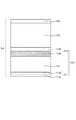
図1は、本実施の形態にかかる有機発光装置を構成する画素の一例を示す断面図である。図1に示した画素は、基板100、トランジスタTr2、多層配線構造102、プラグ103、第一電極110、有機層120、第二電極130、防湿層140、平坦化層150、及びカラーフィルタ160を備えている。基板100としては、例えばシリコン基板を用いることができる。図1において、有機発光素子ELは、第1電極120、有機層120、及び第2電極130を有する。(Embodiment 1)
FIG. 1 is a cross-sectional view showing an example of pixels constituting the organic light emitting device according to the present embodiment. The pixels shown in FIG. 1 include a
図2は、画素200の一例の等価回路図である。本実施形態の有機発光装置は、マトリクス状に配列された複数の画素200を有する表示領域と、表示領域の周辺に配される周辺領域と、を有する。周辺領域には、複数の走査線231に走査信号を出力する走査線駆動回路221、及び複数の信号線232に映像信号を出力する信号線駆動回路222が設けられている。 FIG. 2 is an equivalent circuit diagram of an example of
各画素200は、それぞれ対応する走査線及び信号線に接続され、スイッチング用トランジスタTr1、駆動用トランジスタTr2、保持容量Cs、および有機発光素子ELを有する。ここでは、スイッチング用トランジスタTr1としてN型MOSトランジスタを、駆動用トランジスタTr2としてP型MOSトランジスタを用いる例を示すが、トランジスタTr1及びTr2は、これに限定されない。 Each
スイッチング用トランジスタTr1のゲートは、走査線231に接続され、ソース及びドレインの一方、信号線232に接続される。また、スイッチング用トランジスタTr1のソース及びドレインの他方は、駆動用トランジスタTr2のゲート及び保持容量Csの一方の電極に接続される。保持容量Csの他方の電極及び駆動用トランジスタTr2のソース及びドレインの一方は、電源線Vccに接続される。駆動用トランジスタTr2のソース及びドレインの他方は、有機発光素子ELに接続される。 The gate of the switching transistor Tr1 is connected to the
図2に示す有機発光装置において、走査信号線駆動回路221によりスイッチング用トランジスタTr1がオン状態となることで、信号線232から映像信号が画素200に書き込まれ、書き込まれた映像信号は保持容量Csに保持される。保持された映像信号に応じた電流が、駆動用トランジスタTr2から有機発光素子ELに供給され、この電流に応じた輝度で有機発光素子ELが発光する。なお、ここでは、複数の画素200の駆動用トランジスタTr2及び保持容量Csが、共通の電源線Vccに接続されている例を示す。 In the organic light emitting device shown in FIG. 2, when the switching transistor Tr1 is turned on by the scanning signal
上記の画素回路の構成は一例であり、画素200は、必要に応じて、容量素子やトランジスタをさらに有していてもよい。また周辺回路も、画素の構成に応じて必要となる駆動回路を適宜有することができる。 The configuration of the pixel circuit described above is an example, and the
図2において、トランジスタTr2上に、複数の配線及び複数の層間絶縁層を有する多層配線構造102が形成されている。多層配線構造102の上には、有機発光素子ELの第1電極110が配されている。第1電極110は、多層配線構造102中の配線102及びプラグ103を介して、駆動用トランジスタTr2に接続されている。また、多層配線構造102にMIM容量が容量素子Caとして配されている。 In FIG. 2, a
なお有機発光素子EL等からの光がトランジスタ特性に影響を及ぼさないようにするため、多層配線構造102が遮光層(不図示)を備えていても良い。配線層101の材料として、例えばアルミニウム合金を用いることができ、配線層101を接続するプラグ103の材料として、例えばタングステンを用いることができる。また、層間絶縁膜には、例えば酸化シリコンから成る膜を用いることができる。遮光層の材料としては、例えばチタン(Ti)や窒化チタン(TiN)等を用いることができる。なお、多層配線構造102において、第1電極110の下地となる絶縁層としては、第1電極110の膜厚のバラツキを低減するため、表面が平坦化された無機絶縁膜を用いることが好ましい。 The
基板100、トランジスタ、及び多層配線構造102を回路基板と称する。回路基板上には、有機発光素子ELが配されている。反射型の有機発光装置の有機発光素子ELは、有機層の両側に配される電極のうち一方が反射電極であり、他方が透光性電極であり、有機層で発光した光が一方の電極で反射されて、他方の電極から出射するよう構成されている。ここでは、第1電極110が反射電極であり、第2電極130が透光性電極である有機発光装置について説明する。 The
ここで、反射電極とは、有機発光層が発光する光に対する反射率が50%を超える電極であり、電極が複数の膜が積層された構成を有する場合は、複数の膜を1つの電極としたときの電極の反射率が50%を超えるものとする。また、透光性電極とは、有機発光層が発光する光の透過率が50%を超える電極であり、電極が複数の膜が積層された構成を有する場合は、複数の膜を1つの電極としたときの電極の透光率が50%を超えるものとする。 Here, the reflective electrode is an electrode having a reflectance of more than 50% with respect to the light emitted by the organic light emitting layer, and when the electrode has a configuration in which a plurality of films are laminated, the plurality of films are used as one electrode. It is assumed that the reflectance of the electrode at that time exceeds 50%. The translucent electrode is an electrode having a light transmittance of more than 50% emitted by the organic light emitting layer, and when the electrode has a structure in which a plurality of films are laminated, a plurality of films are combined into one electrode. The light transmittance of the electrode is assumed to exceed 50%.
有機層120は、発光層を有し、たとえば正孔注入層、正孔輸送層、発光層、電子輸送層、電子注入層が積層された構造を有する。有機層120は、この構成に限定されず、正孔注入層、正孔輸送層、電子輸送層、及び電子注入層は、素子の設計に応じて、適宜設ければよい。有機層の各層は、公知の有機材料を適宜用いて形成することができる。 The
第2電極130は、透光性電極であり、導電膜を形成、パターニングすることで形成できる。導電膜としては、例えば、ITO(Indium Tin Oxide)やIZO(Indium Zinc Oxide)などの透明電極材料を用いて形成することができる。また特に有機発光素子がキャビティ構造として構成される場合には、光の干渉を利用するため、第2電極130は、発光層からの光に対する透光性だけでなく、反射性も必要となる。よって、第2電極130として、例えは5〜20nm程度の薄膜のMgAg等の半透過性を有する導電層を用いることができる。なお、キャビティ構造とは、発光層からの光を第1電極110及び第2電極130の間で共振させて、第2電極130側から光を取り出す構造を指す。 The
本実施形態において、第1電極は反射電極であり、少なくとも、金属層と、該金属層の金属より反射率が低い金属を有する混在層と、の積層を有する。物体の反射率は、物体の厚みや波長によって異なる。金属層は、金属光沢を有する。 In the present embodiment, the first electrode is a reflective electrode, and has at least a laminate of a metal layer and a mixed layer having a metal having a reflectance lower than that of the metal of the metal layer. The reflectance of an object depends on the thickness and wavelength of the object. The metal layer has a metallic luster.
本明細書において、金属層(導電層)が金属Aを含み、混合層が金属Aと金属Bの混合層のとき、例えばTEM−EDX分析おいて、金属Bの成分が検出限界(ノイズを含む)以下の部分を金属層(導電層)とする。また、金属Aと金属Bの成分が共に検出限界より大きい値である部分を混合層とする。 In the present specification, when the metal layer (conductive layer) contains the metal A and the mixed layer is a mixed layer of the metal A and the metal B, for example, in the TEM-EDX analysis, the component of the metal B is the detection limit (including noise). ) The following part is a metal layer (conductive layer). Further, the portion where the components of the metal A and the metal B are both larger than the detection limit is defined as the mixed layer.
また、本明細書において、金属や部材の反射率とは、該金属から成る膜や部材の反射率がほぼ一定となるだけの、十分な膜厚の膜(部材)における反射率を指す。金属Aの反射率が金属Bの反射率より大きいとは、金属A単体と金属B単体の膜を、どちらの反射率もほぼ一定となるのに十分な厚さとしたとき、同じ波長に対する金属Aの反射率が金属Bの反射率より大きいことを示す。反射率を検討、比較するときの光の波長としては、各画素の出射光の色に合わせて設定することができる。反射率もほぼ一定となるのに十分な厚さは、例えば0.1mmとすることができる。 Further, in the present specification, the reflectance of a metal or a member refers to the reflectance of a film (member) having a sufficient film thickness so that the reflectance of the film or member made of the metal becomes substantially constant. The fact that the reflectance of the metal A is larger than the reflectance of the metal B means that when the film of the metal A alone and the metal B alone has a thickness sufficient for both reflectances to be substantially constant, the metal A for the same wavelength is used. Indicates that the reflectance of metal B is greater than that of metal B. The wavelength of light when examining and comparing the reflectance can be set according to the color of the emitted light of each pixel. The thickness sufficient for the reflectance to be substantially constant can be, for example, 0.1 mm.
金属層は、反射性の高い金属で形成することができ、例えば、アルミニウム(Al)、銀(Ag)、クロム(Cr),ニッケル(Ni)、白金(Pt)、錫(Sn)またはこれらの金属の合金を用いることができる。好ましくは、AlやAg、及びその合金を用いることができる。金属層とは、金属単体によって構成される導電層たけでなく、その金属の合金によって構成される導電層を含み、製造上、意図せず不純物として入ってしまった他の元素を含んでいてもよい。上記金属より反射率の低い金属としては、例えば、チタン(Ti)、モリブデン(Mo)、タングステン(W)等の高融点金属を用いることができる。 The metal layer can be made of a highly reflective metal, such as aluminum (Al), silver (Ag), chromium (Cr), nickel (Ni), platinum (Pt), tin (Sn) or these. Metal alloys can be used. Preferably, Al, Ag, and an alloy thereof can be used. The metal layer includes not only a conductive layer composed of a single metal but also a conductive layer composed of an alloy of the metal, and may contain other elements that have been unintentionally contained as impurities in manufacturing. good. As the metal having a lower reflectance than the above metal, for example, a refractory metal such as titanium (Ti), molybdenum (Mo), or tungsten (W) can be used.
金属層の金属より反射率が低い金属を有する混在層は、高融点金属と反射性の高い金属の混在層だけでなく、高融点金属の化合物と反射性の高い金属の混在層であってもよい。すなわち、混在層は、金属層の金属中に導電層の金属を含んでいても、導電層の金属中に金属層の金属を含んでいてもよく、また、それらが合金化していても良いし、そうでなくても良い。 The mixed layer having a metal having a lower reflectance than the metal of the metal layer is not only a mixed layer of a refractory metal and a highly reflective metal, but also a mixed layer of a compound of a refractory metal and a highly reflective metal. good. That is, the mixed layer may contain the metal of the conductive layer in the metal of the metal layer, may contain the metal of the metal layer in the metal of the conductive layer, or may be alloyed with them. , It doesn't have to be.
金属層の材料として、アルミニウムや銀といった反射率の高い材料を用いた場合、これらの金属は酸化されやすい。有機発光装置においては、例えば有機層などの第1電極上に配置される酸素を含む材料からの酸素の内方拡散や、は製造工程内での酸素を含む雰囲気での加熱工程による酸素の内方拡散により、金属層が酸化されることがある。 When a material having high reflectance such as aluminum or silver is used as the material of the metal layer, these metals are easily oxidized. In an organic light emitting device, for example, inward diffusion of oxygen from an oxygen-containing material arranged on a first electrode such as an organic layer, or among oxygen produced by a heating process in an oxygen-containing atmosphere in a manufacturing process. The metal layer may be oxidized by the direction diffusion.
そこで、Ti、Mo、W等の高融点金属層を上記金属層上に設けることにより、これらの金属層の酸化を防止することができる。しかし、高融点金属は、アルミニウムや銀等の金属より反射率が低いため、第1電極の反射率は低下してしまう。しかし、単純に高融点金属層の膜厚を薄くすると、高融点金属層内を酸素が拡散し金属層に到達してしまうため、金属層の金属の酸化を抑制することができない。 Therefore, by providing a refractory metal layer such as Ti, Mo, or W on the metal layer, oxidation of these metal layers can be prevented. However, since the refractory metal has a lower reflectance than a metal such as aluminum or silver, the reflectance of the first electrode is lowered. However, if the film thickness of the refractory metal layer is simply reduced, oxygen diffuses in the refractory metal layer and reaches the metal layer, so that the oxidation of the metal in the metal layer cannot be suppressed.
また、金属層と有機層との間の仕事関数を調整するため、第1電極として、金属層と導電層との積層を用いる場合がある。この場合にも、導電層が有する金属の反射率が金属層の金属の反射率より低い場合、第1電極の反射率が低下してしまう。 Further, in order to adjust the work function between the metal layer and the organic layer, a laminate of the metal layer and the conductive layer may be used as the first electrode. Also in this case, if the reflectance of the metal of the conductive layer is lower than the reflectance of the metal of the metal layer, the reflectance of the first electrode is lowered.
そこで、金属層が有する金属より反射率が低い金属と、該金属層の金属と、の混在層を、該金属層と有機層の間に配することで、反射率の低下を抑制しながら、金属層の酸化抑制を行うことができる。また、第1電極の反射率の低下を抑制しながら、反射性の高い金属と導電層の金属との混合比を調整すること等により、仕事関数の調整を行うことができる。よって、導電層の設計パラメータ(材料の種類、比率、膜厚等)の自由度を大きくすることができる。 Therefore, by arranging a mixed layer of a metal having a reflectance lower than that of the metal of the metal layer and the metal of the metal layer between the metal layer and the organic layer, while suppressing a decrease in reflectance, while suppressing a decrease in reflectance. It is possible to suppress the oxidation of the metal layer. Further, the work function can be adjusted by adjusting the mixing ratio of the highly reflective metal and the metal of the conductive layer while suppressing the decrease in the reflectance of the first electrode. Therefore, the degree of freedom of the design parameters (material type, ratio, film thickness, etc.) of the conductive layer can be increased.
また、混在層が含む金属は、金属層の金属でなくてもよい。混在層が、金属層の酸化防止のため設けられる場合には、混在層は、酸化防止のための金属と、その金属より反射率の高い金属と、を含む構成であればよい。また、混在層が、仕事関数の調整のために設けられる場合には、混在層は、仕事関数を調整するための金属と、その金属より反射率が高く仕事関数の調整に適した金属と、を含む構成であればよい。 Further, the metal contained in the mixed layer does not have to be the metal of the metal layer. When the mixed layer is provided to prevent oxidation of the metal layer, the mixed layer may have a structure including a metal for preventing oxidation and a metal having a higher reflectance than the metal. When a mixed layer is provided for adjusting the work function, the mixed layer contains a metal for adjusting the work function and a metal having a higher reflectance than the metal and suitable for adjusting the work function. Any configuration may be used as long as it includes.
以下、本実施形態の有機発光素子の具体的な構成例について説明する。 Hereinafter, a specific configuration example of the organic light emitting device of the present embodiment will be described.
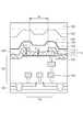
図3を用いて、第1電極の構成について説明する。図3において、第1電極110は、金属層112、混在層113a、導電層113bを有する。金属層112の金属としては、可視光の波長域において反射率の高い材料を用いることができ、例えばAl、Agおよびそれらを含む合金を用いることが出来る。あるいはその他の金属として、Ni、Mo、Cr、Au、Pt、及びそれらを含む合金を用いることもできる。ここでは、金属層112が、Alで形成される例を示す。また金属層112の膜厚は、所望の反射率を得られ、かつ有機層の膜厚よりも薄くなることが好ましい。金属層112の膜厚は、例えば10〜100nmの範囲で設定することができる。なお反射率としては、少なくとも対応する画素の色に対応する波長の光に対し、60%以上であることが好ましい。 The configuration of the first electrode will be described with reference to FIG. In FIG. 3, the
金属層112とその下地となる絶縁層(例えば酸化シリコン膜)との間に、バリアメタル層111を有する構成としてもよい。バリアメタル層111としては、公知の材料を適用することが出来る。ここでは、バリアメタル層111が、Tiから成る第1バリアメタル層111aとTiNから成る第2バリアメタル層111bを有する例を示す。 A
金属層112をAlまたはAl合金を含む層で形成する場合、特にバリアメタル層111を設けることが好ましい。特に、バリアメタル層111としてTi膜を適用することで、属層112のAl膜の配向性が高くなり、表面が平滑な金属層112を形成しやすくなる。よって、金属層112の膜厚の均一性を向上することができ、混在層112aや導電層113bの膜厚を小さくしたい場合にも、金属層112の表面の凹凸に起因する成膜不良を抑制することができる。 When the
導電層113bの材料としては、例えば、Ti、Mo、Wおよびこれらを有する化合物(窒素化合物、酸素化合物)を用いることが出来る。化合物としては、例えばTiNを用いることができる。 As the material of the
混在層113a及び導電層113bの膜厚は、例えば有機層側からの酸素拡散を考慮し、混在層113aと導電層113bの膜厚の和が、酸素が拡散する深さ以上となる膜厚とすることが好ましい。また、金属層112上に混在層113a及び導電層113bを積層した状態での第1電極の反射率が、十分所望の反射率となる膜厚とすることが好ましい。よって、混在層113a及び導電層113bの膜厚は、酸素拡散と反射率とを考慮した膜厚とすることが好ましく、例えば1nm〜20nmとすることができる。なお、第1電極110の反射率としては、少なくとも50%以上であることが好ましい。 The film thickness of the
本実施の形態において、混在層113aとは、金属層112の金属と導電層112bの金属とを含む領域であり、例えば、図3に示すように、金属層112と導電層113bの間に存在する。混在層113aに含まれる高融点金属としては、高融点金属の酸化物の導電率が、金属層112の金属の酸化物の導電率より大きい金属を用いる。また、第1電極110の表層(有機層が形成される側の面)から拡散する酸素の深さに応じて、金属層112の金属が膜厚方向に沿って導電層113b内に分散した混在層113aを、膜厚を調整して形成する。 In the present embodiment, the
金属層112の金属酸化物の絶縁性が大きいと、第1電極110に対する有機層120側表面からの酸素の拡散によって金属層112の導電層113b側の界面一面が酸化されると、第1電極110の導電性が著しく低下する。これより、有機発光装置の駆動電圧が大きくなる。一方、混在層113aに含まれる高融点金属の酸化物の導電率は、金属層112の金属の酸化物の導電率より大きい。本実施の形態の有機発光装置では、第1電極110の表層から拡散する酸素の深さに応じて、金属層112の金属が膜厚方向に沿って導電層113b内に分散した混在層113aを形成する。よって、金属層の表面が一様に酸化されてしまうことを抑制することができる。すなわち、金属層112表面の酸化による第1電極110の導電率の低下を抑制することができる。 When the insulating property of the metal oxide of the
また、導電層113b単層でなく、導電層113bの高融点金属に金属層112の金属が分散されていることで、導電層113bのみで金属層112表面の酸化を抑制する場合に比べ、第1電極110の反射率の低下を抑制することができる。 Further, since the metal of the
混在層113aは、金属層112において、導電層113bとの界面全体または有機層120との界面全体を覆う連続膜として存在してもよいし、不連続な膜として存在してもよい。すなわち、混在層113aが金属層113の導電層113bとの界面または有機層120との界面の一部に配され、金属層112の該界面の一部が混在層113aに覆われていなくてもよい。金属層112の界面の少なくとも一部が混在層113bに覆われていることで、その部分における第1電極110の高抵抗化を抑制することができる。 The
混在層113aは、金属層112の金属及び導電層113bの金属以外の元素を含んでいてもよい。混在層113aが、金属層112の金属及び導電層113bの金属以外の元素を含むことで、酸素の拡散をより抑制することができる場合がある。例えば、金属層112の金属がAlであり、導電層の金属がTiの場合に、混在層113aが窒素有する構成とすることで、金属層112の酸化をより抑制することが可能となる。 The
なお、混在層113aにおいて、導電層113bの金属以外に含まれる金属を、金属層112と異なる金属としてもよい。この時の金属は、導電層113bの金属より反射性の高い金属であればよい。また混在層113aは、導電層113bの金属の代わりに、他の金属を含む構成であってもよい。混在層112aに含まれる金属は、金属層112の金属との、導電性、反射率、及び透過率の関係を考慮して決定することができる。 In the
また混在層112aにおいて、膜厚方向に沿って導電層112bの金属の濃度が変化していてもよい。その場合には、第1電極110の有機層120が配される側の濃度を高くすることが好ましい。これにより混在層113aに含まれる金属層112の金属が酸化される割合を低減することができる。 Further, in the mixed layer 112a, the metal concentration of the conductive layer 112b may change along the film thickness direction. In that case, it is preferable to increase the concentration of the
また図4で示すように、第1電極110は、金属層112及び混在層113aを有し、導電層113bを有していなくてもよい。つまり第1電極110において有機層120と接する面が混在層113aの表面であってもよい。この場合でも、製造工程等における第1電極110への酸素の拡散や第1電極110の反射率を考慮した混在層112bの膜厚とすることで、低消費電極で第1電極110の十分な反射率を確保した有機発光装置を実現することができる。 Further, as shown in FIG. 4, the
表1を用いて、本実施の形態に係る有機発光素子の効果について説明する。 The effect of the organic light emitting device according to the present embodiment will be described with reference to Table 1.
表1に、金属層112にAl合金膜を用い、導電層113bにTi膜を用いた第1電極110を有する有機発光素子における下記項目の関係を示す。項目は、導電層113bの膜厚、混在層113a(AlとTiが混在する領域)の膜厚方向(金属層112と導電層113bの積層報告)の長さである。また、他の項目は、観察波長450nmにおける第1電極110の反射率、及び有機発光素子に電流密度50mA/cm2が流れるときの駆動電圧である。なお、有機発光素子の混在層113a及び導電層113bには、酸素が拡散している。Table 1 shows the relationship between the following items in an organic light emitting device having a
表1において、条件A〜Dは、実施の形態1及び2に記載の有機発光素子の例であり、条件Eは、比較例であり、混在層112bを有さない有機発光素子の場合を示す。反射率及び駆動電圧は、第1電極のみの状態(有機層、第2電極を形成していない状態)で測定した値を示す。 In Table 1, conditions A to D are examples of the organic light emitting devices according to the first and second embodiments, and condition E is a comparative example and shows a case of an organic light emitting device having no mixed layer 112b. .. The reflectance and the driving voltage show the values measured in the state of only the first electrode (the state in which the organic layer and the second electrode are not formed).

表1に示す条件A〜Dの第1電極110の構成においては、導電層113bの膜厚を薄くするほど反射率が高くなった。ただし、混在層113aの膜厚を一定としたまま導電層113bの膜厚を小さくすると、金属層112の酸化により有機発光素子の駆動電圧が上昇する。よって、表1の条件A〜Dでは、導電層113bの膜厚を薄くする場合には、混在層113aの膜厚方向の長さを大きくしている。これにより、条件A〜Dにおける有機発光素子では、有機発光素子に一定の電流を流すために必要な駆動電圧はほぼ同等となった。 In the configurations of the
一方、比較例である条件Eでは、混在層113a及び導電層112bがないため、第1電極110は高い反射率を示しているが、有機発光素子の駆動電圧は上昇してしまった。 On the other hand, under condition E, which is a comparative example, since the
表1より、混在層113aと導電層113bの膜厚の組み合わせを調整することにより、有機発光素子の駆動電圧を上昇させることなく反射率の低下を抑制することができることがわかる。具体的には、第1電極110に対する、有機層120が配される側からの酸素の拡散と、反射率を考慮して、混在層113a、または混在層113aと導電層113bの膜厚の和を調整する。これにより、有機発光素子の駆動電圧を上昇させることなく反射率の低下を抑制することができる。 From Table 1, it can be seen that by adjusting the combination of the film thicknesses of the
また図5に、表1の条件Bの第1電極110の構造における各元素(Al,Ti,O)の第1電極110の深さ方向(膜厚方向)のプロファイルを示す。なおこのプロファイルはTEM−EDX法により測定された結果である。例えば金属層112にAl合金を用い、導電層113bにTiを用いる場合、混在層113aには。AlとTiが含まれる。 Further, FIG. 5 shows a profile of each element (Al, Ti, O) in the structure of the
図5に示すように、第1電極110の表面から10nm付近から導電層113bに含まれるTiが検出されるため、条件Bでは、金属層112の膜厚は10nmである。また、第1電極110の表面から20nm付近でAlが検出限界以下となることから、混合層113aの膜厚方向の長さは、10nmである。 As shown in FIG. 5, since Ti contained in the
次に本実施の形態に係る有機発光装置の一部の製造方法について説明する。 Next, a method for manufacturing a part of the organic light emitting device according to the present embodiment will be described.
シリコン基板100の上に、公知の方法により駆動用トランジスタTr2を形成する。駆動用トランジスタTr2上に層間絶縁膜を形成し、層間絶縁膜内に開口を形成してプラグを形成し、配線層を形成する。層間絶縁膜、プラグ、配線層の形成を繰り返して、多層配線構造102を形成する。多層配線構造102において、最上層の配線層の上に平坦化された絶縁膜を形成し、該平坦化された絶縁膜にプラグ103を形成する。 The driving transistor Tr2 is formed on the
該平坦化された絶縁膜上に、それぞれ、バリアメタル層111、金属層112、導電層113となるバリアメタル膜、金属膜、導電膜をスパッタ等の成膜方法により形成する。バリアメタル層111としては、例えばTiとTiNの積層膜とすることができる。金属層としては、膜厚50nmのAl合金膜を形成し、その上に導電膜として膜厚10nmのTi膜を形成することができる。 A barrier metal film, a metal film, and a conductive film to be the
なお金属層112であるAl合金層の形成後の金属層112の表面の反射率は、90%以上である。また、金属層112上の導電層113となる導電膜(Ti膜)を、形成後の導電層113の表面の反射率が80%以上となるように、Al合金膜およびTi膜の膜厚を調整する。その後350℃の窒素雰囲気で30分間加熱し、混在層113aを形成する。 The reflectance of the surface of the
導電層となる導電膜の形成後に加熱処理を行うことで、導電膜に含まれる金属(Ti)が金属層内に拡散し、AlとTiの混在膜が形成される。加熱温度が低いと、混在層は実質的には形成されない。よって、加熱処理の温度は、300℃以上とすることが好ましい。 By performing the heat treatment after forming the conductive film to be the conductive layer, the metal (Ti) contained in the conductive film is diffused in the metal layer, and a mixed film of Al and Ti is formed. When the heating temperature is low, the mixed layer is substantially not formed. Therefore, the temperature of the heat treatment is preferably 300 ° C. or higher.
この後、金属膜、混在層、及び導電膜をパターニングすることで、金属層112、混在層113a、及び導電層113bを形成することができる。この加熱処理により、導電層113bであるTi膜の膜厚が5nm、混在層113aとなるTiとAlの混在層の膜厚方向の長さが10nm、金属層112であるAl膜の膜厚が45nmとなる。金属層112の酸化抑制のため、混在層の膜厚方向の長さは、10nm以上とすることが好ましい。 After that, the
ここでは、導電層113bとなる導電膜の形成後、加熱処理を行う例を示すが、実施の形態2のように、バンク絶縁層を有する場合は、バンク絶縁層となる絶縁膜の形成と加熱処理を兼ねてもよい。この場合、金属膜及び導電膜をパターニングし、好ましくは300℃以上でバンク絶縁層となる絶縁膜の成膜を行う。この時、混在層113bが形成される。 Here, an example in which heat treatment is performed after the formation of the conductive film to be the
なお、混在層113aは、金属層112を形成するのに用いることのできる金属と導電層113bを形成するのに用いることのできる金属を含む層をスパッタ法により形成しても良い。合金ターゲットによるスパッタでも良いし、2元系スパッタ法で形成しても良い。また金属層112を形成するのに用いることのできる金属と導電層113bを形成するのに用いることのできる金属の割合を膜厚方向に沿って異ならせるように、複数の層を重ねて形成しても良い。 The
金属層112と導電層113aの形成過程においては、その間に大気に暴露することなく積層することで、金属層112の表面が酸化されるのを防止する。その後、フォトリソグラフィー及びウェットエッチングにより、画素毎に分離された第1電極110を形成する。ウェットエッチングにより第1電極110の側面は順テーパーを有する傾斜をもたせ、その上に形成する有機層120や第2電極130の段切れを防止することや、局所的な薄膜化を緩和することができる。したがって、有機層120や第2電極130の段切れを防止することや、局所的な薄膜化を緩和するために第1電極110の膜厚を大きくする必要がない。よって、混在層113a及び導電層113bの膜厚調整の範囲を広げることが可能となる。 In the process of forming the
次に、例えば真空蒸着法により有機層120を、第1電極110及び多層配線構造102上に形成する。有機層120は、発光層を有し、その他に、正孔注入層、正孔輸送層、電子輸送層、電子注入層の少なくとも1つを有していてもよい。なお有機層120を形成したくない領域、たとえば電極パッド部、スクライブ領域(不図示)などはメタルマスク等のマスクを用いて覆っておくことができる。 Next, for example, the
有機層120形成後、例えば蒸着法により、薄膜(例えば、膜厚が約10nm)のAgMgからなる第2電極130を形成する。本実施の形態の有機発光装置では、第1電極110は画素毎に個別に形成されているが、第2電極120は複数の画素間で共通に(連続して)形成されている。 After forming the
次に、例えばCVD法、ALD法などにより、防湿層140を形成する。防湿層140は同一材料からなる単層構造でもよく、より高い防湿性能を備えるために、異なる材料、あるいは膜質の層の積層でも良い。防湿層140は、例えば窒化シリコン(SiN)を用いて形成することができる。 Next, the moisture-
次に、例えば、防湿層140上に、平坦化層150として機能する絶縁膜を形成し、防湿層140の表面の起伏を平坦化した後に、カラーフィルタ層160を形成することができる。次にフォトリソグラフィーとドライエッチング法により防湿層140を除去して電極パッド部(不図示)を露出させる。このようにして、有機発光装置を形成することができる。 Next, for example, the
以上に説明した本実施の形態に係る有機発光装置は、第1電極において、金属層と混在層が積層されているため、第1電極の反射率の低下が抑制された有機発光装置である。また、混在層が金属層の金属と、該金属層の金属の酸化物より酸化物の導電率が高い金属を有することで、駆動電圧の上昇が抑制された有機発光装置である。また、第1電極の反射率の低減を抑制しながら、金属層の酸化による第1電極の抵抗の上昇を抑制することが可能である。 The organic light emitting device according to the present embodiment described above is an organic light emitting device in which a decrease in reflectance of the first electrode is suppressed because a metal layer and a mixed layer are laminated on the first electrode. Further, the mixed layer is an organic light emitting device in which an increase in the driving voltage is suppressed by having a metal of the metal layer and a metal having a higher conductivity of the oxide than the oxide of the metal of the metal layer. Further, it is possible to suppress an increase in the resistance of the first electrode due to oxidation of the metal layer while suppressing a decrease in the reflectance of the first electrode.
本実施の形態では、具体例として、第1電極110の金属層112の酸化を抑制するために混在層113aを配する例について説明しているが、本実施の形態の有機発光装置はこの場合に限定されない。第1電極110の仕事関数を調整するために混在層113aを配する場合であっても、同様の効果が得られる。具体的には、金属層112上に配される仕事関数調整用の層の金属の反射率が、金属層112の金属より低い場合、調整用の金属の単層を金属層112上に設けた場合、第1電極110の反射率が低下する。 In the present embodiment, as a specific example, an example in which the
そこで、第1電極110を、金属層112と、仕事関数調整用の金属及び該調整用の金属より反射率が高い金属との混在層113bと、の積層とすることで、第1電極110の反射率の低下を抑制することができる。例えば、混在層113aは、仕事関数調整用の金属であるチタン(Ti)と、金属層112の金属であって、チタンより反射率が高い金属であるアルミニウム(Al)を含む層とすることができる。これによっても、第1電極110の仕事関数を調整することで、有機発光装置の駆動電圧を下げながら、第1電極110の反射率の低下を抑制することができる。 Therefore, the
(実施の形態2)
本実施の形態における有機発光装置、及びその製造方法について、図6乃至図9を用いて説明する。本実施の形態と実施の形態1との違いは、第一電極の構造が異なる点、及び本実施の形態ではバンク絶縁層を有する点である。なお、実施の形態1と同様の構成、機能、方法、効果については、説明を省略する。(Embodiment 2)
The organic light emitting device and the method for manufacturing the organic light emitting device according to the present embodiment will be described with reference to FIGS. 6 to 9. The difference between the present embodiment and the first embodiment is that the structure of the first electrode is different, and that the present embodiment has a bank insulating layer. The same configuration, function, method, and effect as in the first embodiment will not be described.
図6は本実施の形態にかかる有機発光装置を構成する画素の一部の構造を示す断面図である。図6に示した有機発光装置は、基板110、トランジスタTr2、配線101を有する多層配線構造102、第1電極110、バンク絶縁層117、有機層120、第2電極130、防湿層140、平坦化層150、及びカラーフィルタ160を有する。第1電極110は、画素ごとにパターニングされ、アイランド形状を有している。 FIG. 6 is a cross-sectional view showing a part of the structure of the pixels constituting the organic light emitting device according to the present embodiment. The organic light emitting device shown in FIG. 6 includes a
バンク絶縁層117は、画素ごとに第1電極110の端部(上面における外縁部及びその側面)を覆う絶縁部材である。これにより第1電極110の端部と平面視で重なる領域において、有機層120が薄くなっていたとしても第1電極110や第2電極130とのリークや短絡を低減、防止することができる。ここで、平面視とは、第1電極110の有機層120が配される面に対する平面視を指す。 The
具体的には、バンク絶縁層117は、第1の電極110上に開口Wを有する。このバンク絶縁層117における第1電極110上の開口領域が、有機発光素子ELの発光領域に相当する。このようなバンク絶縁層117は、有機層120と接するため、含水率や透湿性の低い材料を用いて形成されることが好ましい。例えば、バンク絶縁層117は、無機絶縁層とすることができ、具体的には、酸化シリコン、窒化シリコン、及び窒化酸化シリコン(SiON)などの無機絶縁材料を用いて形成することができる。 Specifically, the
第1電電極110は、バンク絶縁層117の開口内において第1の膜厚を有し、バンク絶縁層117に覆われる領域において第1の膜厚より大きい第2の膜厚を有する。 The first
図6に示すように、例えば、導電層113において、バンク絶縁層117の開口W内での膜厚をD1、バンク絶縁層117に覆われる部分の厚さをD2とする。本実施の形態において、第1電極110は、膜厚D1及びD2が、D1<D2の関係を満たすように構成されている。図6では、導電層113が混在層113aのみの場合を示しているが、導電層113は、混在層113aと導電層113bの両方を含んでいてもよく、混在層113aのみであっても良い。 As shown in FIG. 6, for example, in the
具体的には、導電層113が混在層113aのみから構成される場合、混在層113aが、バンク絶縁層117の開口内において、バンク絶縁層117に覆われる領域よりも小さな膜厚を有する。導電層113が混在層113a及び導電層113bから構成される場合、導電層113bがバンク絶縁層117の開口内において、バンク絶縁層117に覆われる領域よりも小さな膜厚を有していてもよい。また、導電層113が混在層113a及び導電層113bを有する一方、開口W内では導電層113bが除去され、混在層114a第1電極110の表面となっていてもよい。すなわち、導電層113が、混在層113aと、バンク絶縁層117の開口と重なる位置に開口を有する導電層113bを有していてもよい。この場合、混在層113aが、バンク絶縁層117の開口内において、バンク絶縁層117に覆われる領域よりも小さな膜厚を有する。 Specifically, when the
例えば、導電層113のバンク絶縁層117の開口内において第1の膜厚D1は、バンク絶縁層117に覆われる領域の膜厚D2の半分程度とすることができる。図6の有機発光装置において、例えば、開口W内の光電層113の膜厚が5nm、バンク絶縁層117に覆われる部分の膜厚が15nmとすることができる。この時、第1電極110は、開口Wにおいて高い反射率を有する。混在層113aへ酸素が拡散した場合でも金属層112の表面全面の酸化を抑制できるよう、混在層113aの膜厚は10nm以上、より好ましくは、5nm以上であることが好ましい。 For example, the first film thickness D1 in the opening of the
バンク絶縁層117を、例えば酸化シリコンで形成する場合、この酸化シリコンが第1電極110への酸素の供給源となり、第1電極110へ拡散する。このため、第1電極110の、バンク絶縁層117と接する領域においては、バンク絶縁層117から拡散する酸素によって金属層112が酸化されないような構成とする。すなわち、混在層113aの膜厚、または混在層113aと導電層113bの膜厚を、酸素が金属層112の表面全体まで到達しない膜厚とすることが好ましい。 When the
ここで、バンク絶縁層117は、絶縁膜がパターニングされることで形成され、開口Wを有し、開口Wの周辺において、第1電極110を覆うよう形成されている。例えば、絶縁層の一部をエッチングにより除去されることで、開口Wが形成される。よって、バンク絶縁層117形成用の絶縁膜に開口Wが形成された後、第1電極110の、開口W内の部分には、酸素の供給源となる絶縁膜(酸化シリコン)がない。よって、金属層112の酸化を防止するための導電層113(混在層113aまたは混在層113a及び導電層113b)を、開口Wがない場合に比べ膜厚を小さくすることができる。開口W内の導電層113の膜厚を小さくいため、発光領域における第1電極110の反射率を高めることができる。 Here, the
また有機発光装置の製造工程において、導電層113内に酸素が多く拡散した状態の場合、導電層113形成の後の製造工程において、導電層113に含まれる酸素が金属層112に拡散し、金属層112を酸化する可能性がある。このため酸素を含む導電層113(混在層113aの膜厚、または混在層113aと導電層113b)を一部除去する。すなわち、混在層113bの膜厚、または混在層113aと導電層113bの膜厚の和が、バンク絶縁層117の開口内において、バンク絶縁層117と平面視において重なる領域より小さい構成とする。これにより、第1電極110の酸化による有機発光装置の駆動電圧の上昇を抑制でき、有機発光装置の信頼性を向上させることができる。また開口W内の混在層113a、または導電層113bの膜厚を実施の形態1の有機発光装置より小さいため、発光領域において、第1電極110の反射率をより高めることもできる。 Further, in the manufacturing process of the organic light emitting device, when a large amount of oxygen is diffused in the
図6に示した有機発光装置の製造方法を、図7を用いて以下に説明する。なお実施の形態1と重複する工程については省略する。 The method for manufacturing the organic light emitting device shown in FIG. 6 will be described below with reference to FIG. 7. The steps that overlap with the first embodiment will be omitted.
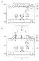
図7(a)に示すように、トランジスタ、及び多層配線構造120が形成された基板100上に、バリアメタル層111となる金属膜、金属層112となる金属膜、導電層113となる導電膜(金属膜)をスパッタ等の成膜方法により形成する。バリアメタル層111としては、例えばTi膜とTiN膜の積層膜を用いることができる。また金属層112としては、例えばAl合金からなる膜を用い、その上にTiからなる薄膜を形成することができる。なおAl合金膜形成後の表面の反射率が90%以上、その上のTi膜を形成後の反射率が80%以上となるように、Al合金膜およびTi膜の膜厚を調整することが好ましい。 As shown in FIG. 7A, a metal film to be a
その後、図7(b)に示すように、フォトリソグラフィー及びドライエッチングにより、バリアメタル層111、金属層112、及び導電層が形成される。これによって、画素毎に分離された、アイランド状の第1電極110が形成される。ドライエッチングでパターニングすることにより、微細な加工が可能である。 Then, as shown in FIG. 7B, the
この時、多層配線層120の最上層の絶縁膜において、第1電極110に上面を覆われていない部分は、ドライエッチング工程におけるオーバーエッチにより、数10nm程度掘り込まれた形状となる。よって、多層配線層120の上面は、第1電極110に覆われた部分と、第1電極110に覆われておらず、凹部となっている部分と、を有する。 At this time, in the insulating film of the uppermost layer of the
次に図8(a)に示すように、第1電極110を含む基板上に、バンク絶縁層117となる絶縁膜(例えば酸化シリコン膜)をCVD法により形成する。CVD法での成膜温度は、300℃以上が好ましく、例えば300℃〜400℃に設定して英膜することができる。この過程で、第1電極110が加熱され、金属層112と導電層113bの間に混在層113aが形成される。よって、混在層113aにおいて、導電層113bの金属の金属層112の金属に対する割合(導電層113bの金属の、混在層113bにおける割合)は、有機層側から金属層側に向かって減少する構成となっていてもよい。 Next, as shown in FIG. 8A, an insulating film (for example, a silicon oxide film) to be the
なお、バンク絶縁層117となる絶縁膜の膜厚は、第1電極110上に形成される有機層120の膜厚よりも薄くすることが好ましい。ただし、絶縁バンク117が第1電極110の端部を被覆できない部分があると、その部分で第1電極110と第2電極130の間にリーク電流の発生や短絡が起こる可能性がある。よって、絶縁バンク117の膜厚は、第1電極110の端部を連続した膜として被覆できる膜厚以上とすることが好ましい。例えば有機層120の膜厚を約200nmとする場合、バンク絶縁層117の膜厚は約70nmとすることができる。 The film thickness of the insulating film to be the
次に図8(b)に示すように、フォトリソグラフィーとドライエッチングにより、絶縁バンク117となる絶縁膜に開口Wを形成し、絶縁バンク117とする。本実施の形態では、開口Wを形成する際、絶縁バンク117となる絶縁膜だけでなく、導電層113の一部も除去される。これにより、第1電電極110は、バンク絶縁層117の開口内において第1の膜厚を有し、バンク絶縁層117に覆われる領域において第1の膜厚より大きい第2の膜厚を有する構造となる。ここで、混在層113aの膜厚が小さいと、拡散した酸素が金属層112表面に達し、金属層112表面の全面を酸化してしまう可能性がある。よって、混在層113aの膜厚方向の長さは、5nm以上、好ましくは10nm以上とすることが好ましい。 Next, as shown in FIG. 8B, an opening W is formed in the insulating film to be the insulating
有機層120を形成する工程以降は、実施の形態1と同様にして有機発光装置を製造することができる。 After the step of forming the
本実施の形態の有機発光装置も、駆動電圧の上昇を抑制、防止しながら、第1電極110の反射率の低下が抑制されている。 The organic light emitting device of the present embodiment also suppresses and prevents an increase in the drive voltage while suppressing a decrease in the reflectance of the
(実施の形態3)
本実施の形態では、実施の形態1または2に記載の有機発光装置を電子機器に適用する例について図9を用いて説明する。(Embodiment 3)
In the present embodiment, an example in which the organic light emitting device according to the first or second embodiment is applied to an electronic device will be described with reference to FIG.
上述した撮像素子をデジタルカメラに適用した実施形態について図9を用いて説明する。レンズ部901は被写体の光学像を撮像素子905に結像させる撮像光学系であり、フォーカスレンズや変倍レンズ、絞りなどを有している。レンズ部901におけるフォーカスレンズ位置、変倍レンズ位置、絞りの開口径などの駆動はレンズ駆動装置902を通じて制御部909によって制御される。 An embodiment in which the above-mentioned image sensor is applied to a digital camera will be described with reference to FIG. The lens unit 901 is an image pickup optical system that forms an optical image of a subject on an image pickup element 905, and includes a focus lens, a variable magnification lens, an aperture, and the like. The drive of the focus lens position, the variable magnification lens position, the aperture diameter of the aperture, and the like in the lens unit 901 is controlled by the control unit 909 through the lens drive device 902.
メカニカルシャッタ903はレンズ部901と撮像素子905の間に配置され、駆動はシャッタ駆動装置904を通じて制御部909によって制御される。撮像素子905は、レンズからの光が入射するように配され、複数の画素によってレンズ部901で結像された光学像を画像信号に変換する。 The mechanical shutter 903 is arranged between the lens unit 901 and the image sensor 905, and the drive is controlled by the control unit 909 through the shutter drive device 904. The image pickup device 905 is arranged so that the light from the lens is incident on the image sensor 905, and converts the optical image formed by the lens unit 901 by the plurality of pixels into an image signal.
信号処理部906は撮像素子905から出力される画像信号が入力され、画像信号にA/D変換、デモザイク処理、ホワイトバランス調整処理、符号化処理などを行う。信号処理部906はまた、撮像素子905の出力する画像信号から得られる信号に基づいて位相差検出方式でデフォーカス量および方向を検出する焦点検出処理も実施する。 The signal processing unit 906 receives an image signal output from the image sensor 905, and performs A / D conversion, demosaic processing, white balance adjustment processing, coding processing, and the like on the image signal. The signal processing unit 906 also performs focus detection processing for detecting the defocus amount and direction by the phase difference detection method based on the signal obtained from the image signal output by the image sensor 905.
タイミング発生部907は撮像素子905および信号処理部906に、各種タイミング信号を出力する。制御部909は、例えばメモリ(ROM,RAM)とマイクロプロセッサ(CPU)を有し、ROMに記憶されたプログラムをRAMにロードしてCPUが実行して各部を制御することにより、デジタルカメラの各種機能を実現する。制御部909が実現する機能には、自動焦点検出(AF)や自動露出制御(AE)が含まれる。制御部909は、撮像素子905から出力された信号に基づいた信号が入力され、また、表示部912に電子ビューファインダー用の信号を入力する。 The timing generation unit 907 outputs various timing signals to the image sensor 905 and the signal processing unit 906. The control unit 909 has, for example, a memory (ROM, RAM) and a microprocessor (CPU), and loads a program stored in the ROM into the RAM, and the CPU executes the program to control each unit. Realize the function. Functions realized by the control unit 909 include automatic focus detection (AF) and automatic exposure control (AE). The control unit 909 inputs a signal based on the signal output from the image sensor 905, and also inputs a signal for the electronic viewfinder to the display unit 912.
メモリ部908は制御部909や信号処理部906が画像データを一時的に記憶したり、作業領域として用いたりする。媒体I/F部910は例えば着脱可能なメモリカードである記録媒体911を読み書きするためのインターフェースである。表示部912は、撮影した画像やデジタルカメラの各種情報を表示するために用いられる。操作部913は電源スイッチ、レリーズボタン、メニューボタンなど、ユーザがデジタルカメラに指示や設定を行うためのユーザインタフェースである。 In the memory unit 908, the control unit 909 and the signal processing unit 906 temporarily store image data or use it as a work area. The medium I / F unit 910 is an interface for reading and writing the recording medium 911, which is a detachable memory card, for example. The display unit 912 is used to display captured images and various information of the digital camera. The operation unit 913 is a user interface for the user to give instructions and settings to the digital camera, such as a power switch, a release button, and a menu button.
表示部912に、実施の形態1または2に記載の有機発光装置を用いることで、消費電力の増加を抑制して、表示部の出射率を向上することができる。よって、明るい場所でも、表示部912に表示された画像の視認性を向上させることができる。 By using the organic light emitting device according to the first or second embodiment for the display unit 912, it is possible to suppress an increase in power consumption and improve the emission rate of the display unit. Therefore, the visibility of the image displayed on the display unit 912 can be improved even in a bright place.
撮影時のデジタルカメラの動作について説明する。電源がオンされると、撮影スタンバイ状態となる。制御部909は、表示部912を電子ビューファインダーとして動作させるための動画撮影処理および表示処理を開始する。撮影スタンバイ状態において撮影準備指示(例えば操作部913のレリーズボタンの半押し)が入力されると、制御部909は焦点検出処理を開始する。例えば、制御部909は、位相差検出方式により焦点検出処理を行うことができる。具体的には、複数の画素から得られるA像信号とB像信号の同種の信号をつなぎ合わせた信号波形の位相差に基づいて像ずれ量を求め、デフォーカス量と方向を得る。 The operation of the digital camera during shooting will be described. When the power is turned on, the shooting standby state is set. The control unit 909 starts a moving image shooting process and a display process for operating the display unit 912 as an electronic viewfinder. When a shooting preparation instruction (for example, half-pressing the release button of the operation unit 913) is input in the shooting standby state, the control unit 909 starts the focus detection process. For example, the control unit 909 can perform the focus detection process by the phase difference detection method. Specifically, the amount of image shift is obtained based on the phase difference of the signal waveform obtained by connecting the signals of the same type of the A image signal and the B image signal obtained from a plurality of pixels, and the defocus amount and the direction are obtained.
そして、制御部909は得られたデフォーカス量と方向とから、レンズ部901のフォーカスレンズの移動量および移動方向を求め、レンズ駆動装置902を通じてフォーカスレンズを駆動し、撮像光学系の焦点を調節する。駆動後、必要に応じてコントラスト評価値に基づく焦点検出をさらに行ってフォーカスレンズ位置を微調整しても良い。 Then, the control unit 909 obtains the moving amount and moving direction of the focus lens of the lens unit 901 from the obtained defocus amount and direction, drives the focus lens through the lens driving device 902, and adjusts the focus of the imaging optical system. do. After driving, the focus lens position may be finely adjusted by further performing focus detection based on the contrast evaluation value, if necessary.
その後、撮影開始指示(例えばレリーズボタンの全押し)が入力されると、制御部909は記録用の撮影動作を実行し、得られた画像データを信号処理部906で処理し、メモリ部908に記憶する。そして、制御部909はメモリ部908に記憶した画像データを、媒体制御I/F部910を通じて記録媒体911に記録する。なお、図示しない外部I/F部から画像データをコンピュータ等の外部装置に出力してもよい。 After that, when a shooting start instruction (for example, full pressing of the release button) is input, the control unit 909 executes a shooting operation for recording, processes the obtained image data in the signal processing unit 906, and causes the memory unit 908. Remember. Then, the control unit 909 records the image data stored in the memory unit 908 on the recording medium 911 through the medium control I / F unit 910. Image data may be output to an external device such as a computer from an external I / F unit (not shown).
112 金属層
113a 混在層
120 有機層
130 第二電極112
Claims (20)
Translated fromJapanese第2電極と、
前記第1電極と前記第2電極の間の、発光層を含む有機層と、
を有し、
前記第1電極の端部は、バンク絶縁層に覆われ、
前記バンク絶縁層は、前記第1電極上に第1開口を有し、
前記有機層は、前記第1開口において、前記第1電極と前記第2電極との間に配され、
前記第1電極は、第1金属を有する金属層と、前記金属層と前記有機層との間の混在層と、を有し、
前記混在層は、前記第1金属と、前記第1金属より反射率の低い第2金属を含み、
前記第1電極は、前記混在層と前記バンク絶縁層の間に配され、前記第2金属を有する導電層を有し、
前記導電層は、前記第1開口と平面視で重なる、第2開口を有することを特徴とする有機発光装置。With the first electrode
With the second electrode
An organic layer containing a light emitting layer between the first electrode and the second electrode,
Have,
The end of the first electrode is covered with a bank insulating layer.
The bank insulating layer has a first opening on the first electrode.
The organic layer is arranged between the first electrode and the second electrode at the first opening.
The first electrode has a metal layer having a first metal and a mixed layer between the metal layer and the organic layer.
The mixed layer isseen containing a first metal, the lower second metal reflective than the firstmetal,
The first electrode is arranged between the mixed layer and the bank insulating layer, and has a conductive layer having the second metal.
An organic light emitting device, wherein the conductive layer has a second opening that overlaps the first opening in a plan view.
第2電極と、
前記第1電極と前記第2電極の間の、発光層を含む有機層と、
を有し、
前記第1電極の端部は、バンク絶縁層に覆われ、前記バンク絶縁層は、前記第1電極上に第1開口を有し、
前記第1電極は、第1金属を有する金属層と、前記金属層と前記有機層との間に配され、前記第1金属及び第2金属を有する混在層と、
を有し、
前記第1電極は、前記混在層と前記バンク絶縁層の間に配され、前記第2金属を有する導電層を有し、
前記導電層は、前記第1開口と平面視で重なる、第2開口を有し、
第1金属はアルミニウムまたは銀であり、
第2金属は、チタン、モリブデン、タングステンの少なくとも1つであることを特徴とする有機発光装置。With the first electrode
With the second electrode
An organic layer containing a light emitting layer between the first electrode and the second electrode,
Have,
The end of the first electrode is covered with a bank insulating layer, and the bank insulating layer has a first opening on the first electrode.
The first electrode is arranged between the metal layer having the first metal and the metal layer and the organic layer, and has a mixed layer having the first metal and the second metal.
Have,
The first electrode is arranged between the mixed layer and the bank insulating layer, and has a conductive layer having the second metal.
The conductive layer has a second opening that overlaps the first opening in a plan view.
The first metal is aluminum or silver,
An organic light emitting devicecharacterized in that the second metal is at least one of titanium, molybdenum, and tungsten.
陰極である第2電極と、
前記第1電極と前記第2電極の間の、発光層を含む有機層と、
を有し、
前記第1電極の端部は、バンク絶縁層に覆われ、
前記バンク絶縁層は、前記第1電極上に第1開口を有し、
前記有機層は、前記第1開口において、前記第1電極と前記第2電極との間に配され、
前記第1電極は、第1金属を有する金属層と、前記金属層と前記有機層との間の混在層と、を有し、
前記混在層は、前記第1金属と、前記第1金属より反射率の低い第2金属を含み、
前記第1電極は、前記混在層と前記バンク絶縁層の間に配され、前記第2金属を有する導電層を有し、
前記導電層は、前記第1開口と平面視で重なる、第2開口を有することを特徴とする有機発光装置。The first electrode, which is the anode, and
The second electrode, which is the cathode,
An organic layer containing a light emitting layer between the first electrode and the second electrode,
Have,
The end of the first electrode is covered with a bank insulating layer.
The bank insulating layer has a first opening on the first electrode.
The organic layer is arranged between the first electrode and the second electrode at the first opening.
The first electrode has a metal layer having a first metal and a mixed layer between the metal layer and the organic layer.
The mixed layer isseen containing a first metal, the lower second metal reflective than the firstmetal,
The first electrode is arranged between the mixed layer and the bank insulating layer, and has a conductive layer having the second metal.
An organic light emitting device, wherein the conductive layer has a second opening that overlaps the first opening in a plan view.
前記バンク絶縁層は、前記第1電極上に第1開口を有し、
前記有機層は、前記第1開口において、前記第1電極と前記第2電極との間に配されていることを特徴とする請求項4または5に記載の有機発光装置。The end of the first electrode is covered with a bank insulating layer.
The bank insulating layer has a first opening on the first electrode.
The organic light emitting device according to claim 4 or 5, wherein the organic layer is arranged between the first electrode and the second electrode at the first opening.
前記多層配線構造の表面の絶縁層は、前記第1電極に覆われていない部分に凹部を有する請求項1乃至17のいずれか1項に記載の有機発光装置。The first electrode is arranged on the multilayer wiring structure.
The organic light emitting device according to any one of claims 1 to 17, wherein the insulating layer on the surface of the multilayer wiring structure has a recess in a portion not covered by the first electrode.
前記レンズからの光が入射する撮像素子と、
前記撮像素子からの出力が入力される制御部と、
前記制御部から信号が入力される、請求項1乃至19のいずれか1項に記載の有機発光装置と、
を有する撮像装置。With the lens
An image sensor that receives light from the lens and
A control unit to which the output from the image sensor is input, and
The organic light emitting device according to any one of claims 1 to 19, wherein a signal is input from the control unit.
An imaging device having.
Priority Applications (2)
| Application Number | Priority Date | Filing Date | Title |
|---|---|---|---|
| JP2017081521AJP6907008B2 (en) | 2017-04-17 | 2017-04-17 | Organic light emitting device, manufacturing method of organic light emitting device, and imaging device |
| US15/950,985US10424757B2 (en) | 2017-04-17 | 2018-04-11 | Organic light emitting apparatus, method for manufacturing organic light emitting apparatus, and imaging apparatus |
Applications Claiming Priority (1)
| Application Number | Priority Date | Filing Date | Title |
|---|---|---|---|
| JP2017081521AJP6907008B2 (en) | 2017-04-17 | 2017-04-17 | Organic light emitting device, manufacturing method of organic light emitting device, and imaging device |
Publications (3)
| Publication Number | Publication Date |
|---|---|
| JP2018181675A JP2018181675A (en) | 2018-11-15 |
| JP2018181675A5 JP2018181675A5 (en) | 2020-05-14 |
| JP6907008B2true JP6907008B2 (en) | 2021-07-21 |
Family
ID=63790950
Family Applications (1)
| Application Number | Title | Priority Date | Filing Date |
|---|---|---|---|
| JP2017081521AActiveJP6907008B2 (en) | 2017-04-17 | 2017-04-17 | Organic light emitting device, manufacturing method of organic light emitting device, and imaging device |
Country Status (2)
| Country | Link |
|---|---|
| US (1) | US10424757B2 (en) |
| JP (1) | JP6907008B2 (en) |
Family Cites Families (13)
| Publication number | Priority date | Publication date | Assignee | Title |
|---|---|---|---|---|
| TW484238B (en)* | 2000-03-27 | 2002-04-21 | Semiconductor Energy Lab | Light emitting device and a method of manufacturing the same |
| US7897979B2 (en)* | 2002-06-07 | 2011-03-01 | Semiconductor Energy Laboratory Co., Ltd. | Light emitting device and manufacturing method thereof |
| JP4401688B2 (en)* | 2002-06-07 | 2010-01-20 | 株式会社半導体エネルギー研究所 | LIGHT EMITTING DEVICE, ITS MANUFACTURING METHOD, AND ELECTRONIC DEVICE |
| JP4495978B2 (en)* | 2003-03-07 | 2010-07-07 | 日東電工株式会社 | ORGANIC ELECTROLUMINESCENT ELEMENT AND SURFACE LIGHT SOURCE AND DISPLAY DEVICE USING THIS ELEMENT |
| CN1638585A (en)* | 2003-12-26 | 2005-07-13 | 日东电工株式会社 | Electroluminescence device, planar light source and display using the same |
| JP5072243B2 (en)* | 2005-03-25 | 2012-11-14 | 株式会社半導体エネルギー研究所 | Light emitting device |
| JP4494369B2 (en)* | 2006-05-24 | 2010-06-30 | 株式会社半導体エネルギー研究所 | Liquid crystal display |
| JP2010153365A (en)* | 2008-11-19 | 2010-07-08 | Semiconductor Energy Lab Co Ltd | Light-emitting element, light-emitting device, electronic equipment, and illumination device |
| WO2012017492A1 (en)* | 2010-08-06 | 2012-02-09 | パナソニック株式会社 | Light emitting element, method for manufacturing same, and light emitting device |
| US8772795B2 (en)* | 2011-02-14 | 2014-07-08 | Semiconductor Energy Laboratory Co., Ltd. | Light-emitting device and lighting device |
| JP6104649B2 (en)* | 2013-03-08 | 2017-03-29 | 株式会社半導体エネルギー研究所 | Light emitting device |
| WO2016063169A1 (en)* | 2014-10-23 | 2016-04-28 | Semiconductor Energy Laboratory Co., Ltd. | Light-emitting element |
| JP2016110904A (en)* | 2014-12-09 | 2016-06-20 | 株式会社Joled | Method for manufacturing organic light-emitting element and organic light-emitting element |
- 2017
- 2017-04-17JPJP2017081521Apatent/JP6907008B2/enactiveActive
- 2018
- 2018-04-11USUS15/950,985patent/US10424757B2/enactiveActive
Also Published As
| Publication number | Publication date |
|---|---|
| US10424757B2 (en) | 2019-09-24 |
| US20180301655A1 (en) | 2018-10-18 |
| JP2018181675A (en) | 2018-11-15 |
Similar Documents
| Publication | Publication Date | Title |
|---|---|---|
| US11004916B2 (en) | Organic light emitting device, image capturing device, and method for producing organic light emitting device | |
| JP6957294B2 (en) | Display devices, electronic devices, and manufacturing methods for display devices | |
| US10644269B2 (en) | Organic light-emitting display device | |
| KR20240134802A (en) | Display unit, method of manufacturing display unit, and electronic apparatus | |
| CN109390376A (en) | Show equipment and its manufacturing method and electronic device | |
| CN110268525B (en) | Image pickup panel and method for manufacturing the same | |
| TW201239855A (en) | Light-emitting display and method of manufacturing the same | |
| TW201023669A (en) | Organic light emitting display device | |
| TW201130372A (en) | Organic light emitting display device | |
| JP2009170395A (en) | Display device and manufacturing method thereof | |
| JP7518680B2 (en) | Organic device, display device, photoelectric conversion device, electronic device, lighting device, lighting fixture for mobile object and mobile object | |
| JP2021039847A (en) | Semiconductor device, light-emitting device, display device, imaging apparatus, electronic apparatus, luminaire, and mobile | |
| JP2011138097A (en) | Display device, method of manufacturing the same, and electronic device | |
| CN111564475B (en) | Electronic devices, display devices, photoelectric conversion devices, electronic devices, lighting equipment, and mobile devices | |
| TW200532919A (en) | Electroluminescent element, and method for fabricating the same and display apparatus | |
| KR20210084766A (en) | Display device and method of manufacturing the same | |
| JP2020136260A (en) | Electronic device, display apparatus, photoelectric conversion apparatus, electronic appliance, lighting apparatus, and moving body | |
| CN113921569A (en) | Organic device and device including the same | |
| JP6907008B2 (en) | Organic light emitting device, manufacturing method of organic light emitting device, and imaging device | |
| KR102756389B1 (en) | Photo transistor and display device comprising of the same | |
| JP7541880B2 (en) | Organic light-emitting device, display device, photoelectric conversion device, electronic device, lighting device, and mobile object | |
| CN1753586B (en) | Manufacturing method of organic electroluminescence display | |
| JP4556768B2 (en) | Organic electroluminescent display | |
| JP2009224118A (en) | Manufacturing method of organic light-emitting element, organic light-emitting display device, manufacturing method of self light-emitting element, and self light-emitting display device | |
| JP7645915B2 (en) | Light-emitting device and its manufacturing method, display device, photoelectric conversion device, electronic device, lighting device, and mobile object |
Legal Events
| Date | Code | Title | Description |
|---|---|---|---|
| A521 | Request for written amendment filed | Free format text:JAPANESE INTERMEDIATE CODE: A523 Effective date:20200401 | |
| A621 | Written request for application examination | Free format text:JAPANESE INTERMEDIATE CODE: A621 Effective date:20200401 | |
| A977 | Report on retrieval | Free format text:JAPANESE INTERMEDIATE CODE: A971007 Effective date:20210120 | |
| A131 | Notification of reasons for refusal | Free format text:JAPANESE INTERMEDIATE CODE: A131 Effective date:20210202 | |
| A521 | Request for written amendment filed | Free format text:JAPANESE INTERMEDIATE CODE: A523 Effective date:20210329 | |
| TRDD | Decision of grant or rejection written | ||
| A01 | Written decision to grant a patent or to grant a registration (utility model) | Free format text:JAPANESE INTERMEDIATE CODE: A01 Effective date:20210601 | |
| A61 | First payment of annual fees (during grant procedure) | Free format text:JAPANESE INTERMEDIATE CODE: A61 Effective date:20210630 | |
| R151 | Written notification of patent or utility model registration | Ref document number:6907008 Country of ref document:JP Free format text:JAPANESE INTERMEDIATE CODE: R151 |