Movatterモバイル変換


[0]ホーム

URL:


JP6903875B2 - Optical scanning device, projector device and head-up display device - Google Patents

Optical scanning device, projector device and head-up display device
Download PDF

Info

Publication number
JP6903875B2
JP6903875B2JP2016132794AJP2016132794AJP6903875B2JP 6903875 B2JP6903875 B2JP 6903875B2JP 2016132794 AJP2016132794 AJP 2016132794AJP 2016132794 AJP2016132794 AJP 2016132794AJP 6903875 B2JP6903875 B2JP 6903875B2
Authority
JP
Japan
Prior art keywords
light
scanned
image
area
scanning direction
Prior art date
Legal status (The legal status is an assumption and is not a legal conclusion. Google has not performed a legal analysis and makes no representation as to the accuracy of the status listed.)
Active
Application number
JP2016132794A
Other languages
Japanese (ja)
Other versions
JP2018005007A (en
Inventor
赤沼 悟一
悟一 赤沼
Current Assignee (The listed assignees may be inaccurate. Google has not performed a legal analysis and makes no representation or warranty as to the accuracy of the list.)
Ricoh Co Ltd
Original Assignee
Ricoh Co Ltd
Priority date (The priority date is an assumption and is not a legal conclusion. Google has not performed a legal analysis and makes no representation as to the accuracy of the date listed.)
Filing date
Publication date
Application filed by Ricoh Co LtdfiledCriticalRicoh Co Ltd
Priority to JP2016132794ApriorityCriticalpatent/JP6903875B2/en
Priority to EP17178567.8Aprioritypatent/EP3267236B1/en
Publication of JP2018005007ApublicationCriticalpatent/JP2018005007A/en
Application grantedgrantedCritical
Publication of JP6903875B2publicationCriticalpatent/JP6903875B2/en
Activelegal-statusCriticalCurrent
Anticipated expirationlegal-statusCritical

Links

Images

Classifications

Landscapes

Description

Translated fromJapanese

本発明は、光走査装置、プロジェクタ装置およびヘッドアップディスプレイ装置に関する。 The present invention relates to an optical scanning device, a projector device and a head-up display device.

従来、例えばMEMSプロセスにより作製されたMEMSミラーを光偏向器として用い、この光偏向器により光源からのレーザ光を偏向して被走査面上で二次元方向(主走査方向および副走査方向)に走査させることで画像を描画する光走査装置が知られている。 Conventionally, for example, a MEMS mirror manufactured by a MEMS process is used as an optical deflector, and the laser beam from a light source is deflected by this optical deflector in two-dimensional directions (main scanning direction and sub-scanning direction) on the surface to be scanned. An optical scanning device that draws an image by scanning is known.

この種の光走査装置では、光偏向器に対する印加電圧を一定に保っていても、例えば温度変動や経時変化などによって光偏向器の共振周波数に対する振幅感度が変化するなどの要因により、光偏向器の振幅量が変動する。このため、被走査面上を走査したレーザ光を検出するための光検出器を設け、この光検出器がレーザ光を検出したタイミングに基づいて光偏向器の振幅を制御することが提案されている(例えば、特許文献1、特許文献2等を参照)。 In this type of optical scanning device, even if the voltage applied to the optical deflector is kept constant, the optical deflector is affected by factors such as changes in the amplitude sensitivity of the optical deflector with respect to the resonance frequency due to temperature fluctuations and changes over time. The amount of amplitude of is fluctuates. Therefore, it has been proposed to provide a photodetector for detecting the laser beam scanned on the surface to be scanned, and to control the amplitude of the optical deflector based on the timing at which the photodetector detects the laser beam. (See, for example, Patent Document 1,Patent Document 2, etc.).

被走査面上を走査したレーザ光を光検出器により検出するには、被走査面上のレーザ光が走査される範囲(以下、これを「光走査範囲」と呼ぶ)内に、光検出器によりレーザ光を検出するための領域(以下、これを「検出領域」と呼ぶ)を設ける必要がある。例えば特許文献1に記載の装置では、被走査面となるレンズアレイ上の光走査範囲内において、画像描画に用いる画像描画領域、つまり、画像情報に応じて変調されたレーザ光が照射される画像描画領域に対して主走査方向に外れた位置に、光検出器を設けている(特許文献1の図4参照)。また、特許文献2に記載の装置では、被走査面となるカバーガラス上の光走査範囲内において、画像描画領域に対して副走査方向に外れた位置に、レーザ光を反射して光検出器に入射させるための反射部が設けられている(特許文献2の図4参照)。 In order to detect the laser beam scanned on the surface to be scanned by the photodetector, the photodetector is within the range in which the laser beam on the surface to be scanned is scanned (hereinafter, this is referred to as "optical scanning range"). It is necessary to provide a region for detecting the laser beam (hereinafter, this is referred to as a “detection region”). For example, in the apparatus described in Patent Document 1, an image drawing region used for image drawing, that is, an image irradiated with laser light modulated according to image information, within an optical scanning range on a lens array to be scanned. A photodetector is provided at a position deviating from the drawing area in the main scanning direction (see FIG. 4 of Patent Document 1). Further, in the apparatus described inPatent Document 2, a photodetector that reflects laser light at a position deviated from the image drawing region in the sub-scanning direction within the optical scanning range on the cover glass to be scanned. (See FIG. 4 of Patent Document 2).

しかし、特許文献1や特許文献2の構成では、光走査範囲における画像描画領域の割合が小さくなるため、特に機械的な制約によって最大振幅量が制限されるMEMSミラーを光偏向器として用いる場合、画角を大きくすることが難しいという問題があった。 However, in the configurations of Patent Document 1 andPatent Document 2, since the ratio of the image drawing area in the optical scanning range is small, especially when a MEMS mirror whose maximum amplitude amount is limited by mechanical restrictions is used as an optical deflector. There was a problem that it was difficult to increase the angle of view.

上述した課題を解決するため、本発明は、光源と、前記光源からの光を偏向して被走査面上で主走査方向および副走査方向に走査させる光偏向器と、前記被走査面上を走査した光を検出する光検出器と、前記光検出器が光を検出したタイミングに基づいて、前記光源の動作と前記光偏向器の動作との少なくとも一方を制御するコントローラと、を備え、前記被走査面上の光が走査される範囲である光走査範囲の主走査方向の端部に、前記光検出器により光を検出するための検出領域を有し、前記光走査範囲内の画像描画に用いる画像描画領域が、前記検出領域に対して主走査方向に隣接する領域と、前記検出領域に対して副走査方向に隣接する領域とを含み、前記被走査面は、マイクロレンズアレイを有する中間スクリーンであり、前記中間スクリーン上の前記光走査範囲の少なくとも主走査方向の端部に、光を反射して前記光検出器に入射させる反射部が設けられ、前記検出領域は、前記反射部が設けられた前記中間スクリーン上の領域であり、前記反射部は、前記マイクロレンズアレイを構成するマイクロレンズの配列ピッチと略等しい間隔で設けられた複数の反射面を含むことを特徴とする。In order to solve the above-mentioned problems, the present invention comprises a light source, an optical deflector that deflects the light from the light source to scan in the main scanning direction and the sub-scanning direction on the scanned surface, and the scanned surface. A light detector that detects scanned light and a controller that controls at least one of the operation of the light source and the operation of the light deflector based on the timing at which the light detector detects light are provided.the end of the main scanning direction of the optical scanning range in the range of light on the surface to be scanned isscanned, has a detection area for detecting the light by the light detector, the image drawing in the optical scanning range image drawing area used for includes aregion adjacent to the main scanning direction with respect to the detection region, and aregion adjacent to the sub-scanning direction with respect to the detection region,the surface to be scanned has a microlens array An intermediate screen, at least at the end of the optical scanning range on the intermediate screen in the main scanning direction, a reflecting portion that reflects light and causes it to enter the light detector is provided, and the detecting region is the reflecting portion. Is a region on the intermediate screen provided with, and the reflecting portion includes a plurality of reflecting surfaces provided at intervals substantially equal to the arrangement pitch of the microlenses constituting the microlens array .

本発明によれば、光走査範囲における画像描画領域の割合を大きくして、画角を大きくすることができるという効果を奏する。 According to the present invention, it is possible to increase the ratio of the image drawing area in the optical scanning range to increase the angle of view.

図1は、第1の実施形態に係るプロジェクタ装置の概略構成を示す図である。FIG. 1 is a diagram showing a schematic configuration of a projector device according to the first embodiment.図2は、光偏向器の具体例を示す図である。FIG. 2 is a diagram showing a specific example of the light deflector.図3は、被走査面となる光透過部材の光偏向器側の面を示す平面図である。FIG. 3 is a plan view showing a surface of the light transmitting member to be scanned on the light deflector side.図4は、光走査範囲のレイアウトを示す図である。FIG. 4 is a diagram showing a layout of an optical scanning range.図5は、レーザ駆動信号のタイミングを説明する図である。FIG. 5 is a diagram illustrating the timing of the laser drive signal.図6は、第2の実施形態に係るプロジェクタ装置の概略構成を示す図である。FIG. 6 is a diagram showing a schematic configuration of the projector device according to the second embodiment.図7は、中間スクリーンの具体例を示す図である。FIG. 7 is a diagram showing a specific example of the intermediate screen.図8は、中間スクリーンと光検出器との位置関係を説明する図である。FIG. 8 is a diagram illustrating the positional relationship between the intermediate screen and the photodetector.図9は、図8における中間スクリーンの右側を拡大して示す図である。FIG. 9 is an enlarged view showing the right side of the intermediate screen in FIG.図10は、光走査範囲のレイアウトを示す図である。FIG. 10 is a diagram showing a layout of an optical scanning range.図11は、中間スクリーンの変形例を説明する図である。FIG. 11 is a diagram illustrating a modified example of the intermediate screen.図12は、中間スクリーンの変形例を説明する図である。FIG. 12 is a diagram illustrating a modified example of the intermediate screen.図13は、中間スクリーンの変形例を説明する図である。FIG. 13 is a diagram illustrating a modified example of the intermediate screen.図14は、中間スクリーンの変形例を説明する図である。FIG. 14 is a diagram illustrating a modified example of the intermediate screen.図15は、レーザ光源および光偏向器を含む光学ユニットの一例を示す図である。FIG. 15 is a diagram showing an example of an optical unit including a laser light source and a light deflector.図16は、第3の実施形態に係るヘッドアップディスプレイ装置の概略構成を示す図である。FIG. 16 is a diagram showing a schematic configuration of a head-up display device according to a third embodiment.図17は、ヘッドアップディスプレイ装置を搭載した車両の概念図である。FIG. 17 is a conceptual diagram of a vehicle equipped with a head-up display device.図18は、ヘッドアップディスプレイ装置が備える光走査装置の概略構成を示す図である。FIG. 18 is a diagram showing a schematic configuration of an optical scanning device included in the head-up display device.図19は、中間スクリーンに描画されて車両のフロントガラスに投射される画像の一例を示す図である。FIG. 19 is a diagram showing an example of an image drawn on the intermediate screen and projected on the windshield of the vehicle.図20は、中間スクリーンに描画されて車両のフロントガラスに投射される画像の一例を示す図である。FIG. 20 is a diagram showing an example of an image drawn on the intermediate screen and projected on the windshield of the vehicle.図21は、中間スクリーンに描画されて車両のフロントガラスに投射される画像の一例を示す図である。FIG. 21 is a diagram showing an example of an image drawn on the intermediate screen and projected on the windshield of the vehicle.

以下、添付図面を参照しながら、本発明に係る光走査装置、プロジェクタ装置およびヘッドアップディスプレイ装置の具体的な実施形態について詳細に説明する。 Hereinafter, specific embodiments of the optical scanning device, the projector device, and the head-up display device according to the present invention will be described in detail with reference to the accompanying drawings.

<第1の実施形態>
図1は、第1の実施形態に係るプロジェクタ装置100Aの概略構成を示す図である。本実施形態のプロジェクタ装置100Aは、図1に示すように、光走査装置10Aと、画像処理装置30とを備える。画像処理装置30は、例えばPC(パーソナルコンピュータ)などの上位装置からの画像情報に対し、投影画像として表示するための各種の画像処理を施して光走査装置10Aに入力する。
<First Embodiment>
FIG. 1 is a diagram showing a schematic configuration of theprojector device 100A according to the first embodiment. As shown in FIG. 1, theprojector device 100A of the present embodiment includes an optical scanning device 10A and animage processing device 30. Theimage processing device 30 performs various image processing for displaying as a projected image on image information from a higher-level device such as a PC (personal computer) and inputs the image information to the optical scanning device 10A.

光走査装置10Aは、光学系の構成要素として、レーザ光源11、コリメートレンズ12、光偏向器13、および光検出器14を備える。また、光走査装置10Aは、制御系の構成要素として、検出アンプ16、コントローラ17、光源ドライバ18、および駆動ドライバ19を備える。 The optical scanning device 10A includes alaser light source 11, acollimating lens 12, alight deflector 13, and aphotodetector 14 as components of the optical system. Further, the optical scanning device 10A includes adetection amplifier 16, acontroller 17, alight source driver 18, and a drive driver 19 as components of the control system.

レーザ光源11は、コントローラ17による制御に応じて、光源ドライバ18の駆動によりレーザ光を出射する。レーザ光源11から出射したレーザ光は、コリメートレンズ12により略平行光にされて光偏向器13に入射する。 Thelaser light source 11 emits laser light by driving thelight source driver 18 in response to control by thecontroller 17. The laser light emitted from thelaser light source 11 is converted into substantially parallel light by the collimatedlens 12 and incident on thelight deflector 13.

光偏向器13は、コントローラ17による制御に応じて、駆動ドライバ19の駆動により直交した2つの方向に所定角度(例えば数deg〜10数deg程度)の振幅で振動し、レーザ光源11からのレーザ光を被走査面上で二次元方向(主走査方向および副走査方向)に走査させる。本実施形態では光偏向器13として、レーザ光を二次元走査するMEMSミラーを用いることを想定するが、一次元走査のものを2つ組み合わせて光偏向器13を構成してもよい。また、片方の走査はポリゴンミラーなどの回転走査ミラーを使用することもできる。 Theoptical deflector 13 vibrates in two directions orthogonal to each other by the drive of the drive driver 19 with an amplitude of a predetermined angle (for example, about several deg to several deg) according to the control by thecontroller 17, and the laser from thelaser light source 11 Light is scanned on the surface to be scanned in two-dimensional directions (main scanning direction and sub-scanning direction). In the present embodiment, it is assumed that the MEMS mirror that scans the laser beam two-dimensionally is used as theoptical deflector 13, but theoptical deflector 13 may be configured by combining two ones that scan one-dimensionally. Further, a rotary scanning mirror such as a polygon mirror can be used for one scanning.

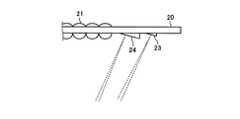
本実施形態では、光走査装置10Aの出射口がカバーガラスなどの光透過部材15で覆われており、この光透過部材15の光偏向器13側の面が、レーザ光が走査される被走査面とされているものとする。そして、被走査面となる光透過部材15の光偏向器13側の面に、光検出器14が設けられている。 In the present embodiment, the outlet of the light scanning device 10A is covered with alight transmitting member 15 such as a cover glass, and the surface of thelight transmitting member 15 on thelight deflector 13 side is scanned by the laser beam. It is assumed that it is a surface. Aphotodetector 14 is provided on the surface of thelight transmitting member 15 to be scanned on thelight deflector 13 side.

光検出器14は、光偏向器13によって被走査面上を走査されたレーザ光を検出するものであり、例えば、レーザ光が受光部を横切るタイミングで電気信号を出力するフォトディテクタなどが用いられる。光検出器14の出力は検出アンプ16により増幅されてコントローラ17に入力される。コントローラ17は、この光検出器14の出力に応じて駆動ドライバ19に供給する光偏向器13の駆動信号を制御することで、光偏向器13の動作を安定させている。 Thephotodetector 14 detects the laser beam scanned on the surface to be scanned by thephotodetector 13, and for example, a photodetector that outputs an electric signal at the timing when the laser beam crosses the light receiving portion is used. The output of thephotodetector 14 is amplified by thedetection amplifier 16 and input to thecontroller 17. Thecontroller 17 stabilizes the operation of theoptical deflector 13 by controlling the drive signal of theoptical deflector 13 supplied to the drive driver 19 according to the output of thephotodetector 14.

また、コントローラ17は、被走査面上を走査するレーザ光により画像処理装置30からの画像情報に応じた画像が被走査面上に描画されるように、光偏向器13の動作に合せてレーザ光源11の動作を制御する。すなわち、コントローラ17は、光偏向器13によって被走査面上に走査されるタイミングに合わせて、画像情報に応じて強度変調されたレーザ光がレーザ光源11から出射されるように、光源ドライバ18を制御する。強度変調はパルス幅を変調してもよいし、振幅を変調してもよい。この変調された信号を光源ドライバ18によりレーザを駆動できる電流に変換してレーザ光源11を駆動している。 Further, thecontroller 17 lasers in accordance with the operation of thelight deflector 13 so that an image corresponding to the image information from theimage processing device 30 is drawn on the scanned surface by the laser beam scanning on the scanned surface. Controls the operation of thelight source 11. That is, thecontroller 17 sets thelight source driver 18 so that the laser light whose intensity is modulated according to the image information is emitted from thelaser light source 11 at the timing when thelight deflector 13 scans the surface to be scanned. Control. Intensity modulation may modulate the pulse width or the amplitude. The modulated signal is converted into a current capable of driving the laser by thelight source driver 18 to drive thelaser light source 11.

本実施形態のプロジェクタ装置100Aは、画像情報に応じたレーザ光の二次元走査により被走査面(光透過部材15の光偏向器13側の面)上に描画された画像をスクリーン40に投影することで、スクリーン40に投影画像を表示する。なお、光透過部材15の代わりに、例えば液晶パネルなどの光変調器を配置し、この光変調器に入射するレーザ光を画像情報に応じて変調して、スクリーン40に投影する構成であってもよい。この場合、レーザ光が入射する光変調器の入射面が被走査面となる。 Theprojector device 100A of the present embodiment projects an image drawn on the surface to be scanned (the surface of thelight transmitting member 15 on thelight deflector 13 side) by two-dimensional scanning of laser light according to the image information on thescreen 40. As a result, the projected image is displayed on thescreen 40. A light modulator such as a liquid crystal panel is arranged instead of thelight transmitting member 15, and the laser light incident on the light modulator is modulated according to the image information and projected onto thescreen 40. May be good. In this case, the incident surface of the light modulator on which the laser light is incident becomes the scanned surface.

図2は、レーザ光源11からのレーザ光を被走査面上で二次元方向に走査させる光偏向器13の具体例を示す図である。図2に示す光偏向器13はMEMSミラーとして構成された光偏向器13の例である。 FIG. 2 is a diagram showing a specific example of thelight deflector 13 that scans the laser beam from thelaser light source 11 in the two-dimensional direction on the surface to be scanned. Thelight deflector 13 shown in FIG. 2 is an example of thelight deflector 13 configured as a MEMS mirror.

図2に示す光偏向器13は、シリコン構造部材の片面に圧電材料が積層されたユニモルフ構造を有し、電圧印加によって駆動梁が変形することで動作する。この光偏向器13は、レーザ光を反射させるミラー部51が、入れ子構造によって直交した2つの方向に回転振動可能に、固定ベース56に対して支持されている。ミラー部51が回転振動する直交した2つの方向のうちの一方が、被走査面上でレーザ光が走査される主走査方向に対応し、他方が、被走査面上でレーザ光が走査される副走査方向に対応している。 Theoptical deflector 13 shown in FIG. 2 has a unimorph structure in which a piezoelectric material is laminated on one side of a silicon structural member, and operates by deforming a drive beam by applying a voltage. In thelight deflector 13, themirror portion 51 that reflects the laser beam is supported with respect to the fixedbase 56 so that themirror portion 51 can rotate and vibrate in two directions orthogonal to each other by the nested structure. One of the two orthogonal directions in which themirror portion 51 rotates and vibrates corresponds to the main scanning direction in which the laser beam is scanned on the scanned surface, and the other corresponds to the main scanning direction in which the laser beam is scanned on the scanned surface. It corresponds to the sub-scanning direction.

ミラー部51を直接支持する内側の支持構造は主走査軸(高速軸)であり、外側の支持構造は副走査軸(低速軸)である。主走査軸は、主走査駆動梁53に対する電圧印加によりトーションバースプリング52が捩れることでミラー部51を振動させる。主走査軸の駆動は、ミラー部51が振動する振動モードの共振周波数の正弦波状の電圧を印加する正弦波駆動(共振駆動)であり、共振動作を利用することで効率よくミラー部51を振動させるようにしている。一方、副走査軸は、副走査駆動梁55に対する電圧印加により可動枠54が傾斜することでミラー部51を振動させる。主走査軸の駆動は、鋸波の電圧を印加する鋸波駆動(非共振駆動)である。ユニモルフ構造における変形量は小さいため、非共振動作の副走査軸は大きな振幅を得ることが難しい。そのため、副走査駆動梁55は、駆動梁が屈曲して連結された回転振幅を累積する構造(ミアンダ構造)となっている。 The inner support structure that directly supports themirror portion 51 is the main scanning axis (high-speed axis), and the outer support structure is the sub-scanning axis (low-speed axis). The main scanning shaft vibrates themirror portion 51 by twisting thetorsion bar spring 52 by applying a voltage to the mainscanning drive beam 53. The drive of the main scanning axis is a sinusoidal drive (resonance drive) in which a sinusoidal voltage of the resonance frequency of the vibration mode in which themirror portion 51 vibrates is applied, and themirror portion 51 is efficiently vibrated by using the resonance operation. I try to let you. On the other hand, the sub-scanning shaft vibrates themirror portion 51 by inclining themovable frame 54 by applying a voltage to thesub-scanning drive beam 55. The drive of the main scanning shaft is a sawtooth drive (non-resonant drive) in which a sawtooth voltage is applied. Since the amount of deformation in the unimorph structure is small, it is difficult to obtain a large amplitude for the sub-scanning axis of non-resonant operation. Therefore, thesub-scanning drive beam 55 has a structure (munder structure) in which the drive beams are bent and connected to accumulate the rotational amplitudes.

以上のように構成される光偏向器13は、温度や環境によって圧電材料や構造部シリコン材料の物性値などが変動するため、一定の電圧振幅を与えていてもミラー部51の振幅が変動してしまう。そのため、光偏向器13により被走査面上を走査したレーザ光を検出する光検出器14を設け、この光検出器14がレーザ光を検出したタイミングに基づいて光偏向器13の動作を制御することにより、安定した光走査を行えるようにしている。 In theoptical deflector 13 configured as described above, since the physical property values of the piezoelectric material and the silicon material of the structural portion fluctuate depending on the temperature and environment, the amplitude of themirror portion 51 fluctuates even if a constant voltage amplitude is applied. It ends up. Therefore, aphotodetector 14 that detects the laser beam scanned on the surface to be scanned by theoptical deflector 13 is provided, and the operation of theoptical deflector 13 is controlled based on the timing at which thephotodetector 14 detects the laser beam. This enables stable optical scanning.

被走査面上を走査したレーザ光を光検出器14により検出するには、被走査面上のレーザ光が走査される範囲である光走査範囲内に、光検出器14によりレーザ光を検出するための領域である検出領域を設ける必要がある。このため、被走査面上を走査したレーザ光により画像を描画するための領域である画像描画領域が検出領域によって制限されることになるが、本実施形態では、光走査範囲内にできるだけ大きな画像描画領域を確保できるように、検出領域と画像描画領域とをレイアウトしている。 In order to detect the laser beam scanned on the surface to be scanned by thephotodetector 14, thephotodetector 14 detects the laser beam within the optical scanning range in which the laser beam on the surface to be scanned is scanned. It is necessary to provide a detection area which is an area for the purpose. Therefore, the image drawing area, which is an area for drawing an image by the laser beam scanned on the scanned surface, is limited by the detection area, but in the present embodiment, the image is as large as possible within the optical scanning range. The detection area and the image drawing area are laid out so that the drawing area can be secured.

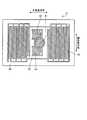
図3は、本実施形態の光走査装置10Aにおいて被走査面となる光透過部材15の光偏向器13側の面を示す平面図であり、図4は、本実施形態における光走査範囲60のレイアウトを示す図である。本実施形態では、例えば図3に示すように、被走査面上で二次元走査されるレーザ光を主走査方向の両端部および副走査方向の一方の端部で検出できるように、図の上側の主走査方向の両端部でレーザ光の軌跡STと重なる位置に、それぞれ光検出器14を配置している。したがって、図4に示すように、光走査範囲60の上側左右両端部が検出領域61とされる。そして、本実施形態では、光走査範囲60の検出領域61を除いたすべての領域を、被走査面上を走査したレーザ光により画像を描画するための画像描画領域62としている。つまり、画像描画領域62が、検出領域61に対して主走査方向に隣接する領域と、検出領域61に対して副走査方向に隣接する領域とを含む構成としている。 FIG. 3 is a plan view showing a surface of thelight transmitting member 15 to be scanned in the optical scanning device 10A of the present embodiment on thelight deflector 13 side, and FIG. 4 is a plan view of theoptical scanning range 60 of the present embodiment. It is a figure which shows the layout. In the present embodiment, for example, as shown in FIG. 3, the upper side of the drawing is such that the laser beam scanned two-dimensionally on the surface to be scanned can be detected at both ends in the main scanning direction and one end in the sub-scanning direction.Photodetectors 14 are arranged at both ends of the main scanning direction at positions overlapping with the laser beam locus ST. Therefore, as shown in FIG. 4, the upper left and right ends of theoptical scanning range 60 are defined as thedetection area 61. Then, in the present embodiment, all the regions except thedetection region 61 of theoptical scanning range 60 are set as animage drawing region 62 for drawing an image by the laser beam scanned on the scanned surface. That is, theimage drawing area 62 includes an area adjacent to thedetection area 61 in the main scanning direction and an area adjacent to thedetection area 61 in the sub-scanning direction.

特許文献1で開示される従来技術では、上述したように、画像描画領域に対して主走査方向に外れた位置を検出領域としているため、検出領域に対して副走査方向に隣接する領域が画像描画領域に含まれない。また、特許文献2で開示される従来技術では、上述したように、画像描画領域に対して副走査方向に外れた位置を検出領域としているため、検出領域に対して主走査方向に隣接する領域が画像描画領域に含まれない。このように従来技術では、光走査範囲内の検出領域に対して主走査方向に隣接する領域、あるいは副走査方向に隣接する領域が画像描画領域に含まれない構成となっている。このため、光走査範囲における画像描画領域の割合が小さく、画角を大きくすることが難しい。 In the prior art disclosed in Patent Document 1, as described above, since the detection region is a position deviated from the image drawing region in the main scanning direction, the region adjacent to the detection region in the sub-scanning direction is an image. Not included in the drawing area. Further, in the prior art disclosed inPatent Document 2, as described above, since the detection area is a position deviated from the image drawing area in the sub-scanning direction, the area adjacent to the detection area in the main scanning direction. Is not included in the image drawing area. As described above, in the prior art, the image drawing area does not include the area adjacent to the detection area in the optical scanning range in the main scanning direction or the area adjacent to the sub-scanning direction. Therefore, the ratio of the image drawing area in the optical scanning range is small, and it is difficult to increase the angle of view.

これに対して本実施形態では、光走査範囲60内の画像描画領域62が、検出領域61に対して主走査方向に隣接する領域と、検出領域61に対して副走査方向に隣接する領域とを含む構成としている。このため、光走査範囲60における画像描画領域62の割合を大きくすることができ、光偏向器13の振幅が同じであったとしても、光走査範囲60内に従来技術よりも広い画像描画領域62を確保して、スクリーン40に表示される投影画像の画角を大きくすることができる。 On the other hand, in the present embodiment, theimage drawing area 62 in theoptical scanning range 60 is an area adjacent to thedetection area 61 in the main scanning direction and an area adjacent to thedetection area 61 in the sub-scanning direction. It is configured to include. Therefore, the ratio of theimage drawing area 62 in theoptical scanning range 60 can be increased, and even if the amplitude of theoptical deflector 13 is the same, theimage drawing area 62 wider than the conventional technique is within theoptical scanning range 60. Can be secured to increase the angle of view of the projected image displayed on thescreen 40.

なお、本実施形態のように、光走査範囲60の検出領域61を除いたすべての領域を画像描画領域62とする構成では、画像描画領域62の形状が従来技術のように単純な矩形ではなくなる。このため、画像描画領域62全体に単一の画像を描画しようとすると、画像に欠落などが生じて視認性の低下を招く場合がある。しかし、例えば検出領域61の位置を基準として画像描画領域62を複数の描画領域に分割し、互いに異なる種類の画像をそれぞれの描画領域に描画する構成とすることにより、画像描画領域62の形状に合わせた適切な画像の描画を行うことができる。 In the configuration in which all the areas other than thedetection area 61 of theoptical scanning range 60 are set as theimage drawing area 62 as in the present embodiment, the shape of theimage drawing area 62 is not a simple rectangle as in the prior art. .. Therefore, if an attempt is made to draw a single image over the entireimage drawing area 62, the image may be missing or the like, resulting in a decrease in visibility. However, for example, by dividing theimage drawing area 62 into a plurality of drawing areas based on the position of thedetection area 61 and drawing different types of images in each drawing area, the shape of theimage drawing area 62 can be obtained. It is possible to draw an appropriate combined image.

例えば図4に示した例では、画像描画領域62を検出領域61に対して副走査方向に隣接する領域を含むメイン描画領域63と、検出領域61に対して主走査方向に隣接する領域を含むサブ描画領域64とに分割する。そして、メイン描画領域63には、画像サイズが比較的大きい主要な画像を描画し、サブ描画領域64には、画像サイズが比較的小さいアイコンや文字画像などの副次的な画像を描画するといった利用方法が考えられる。プロジェクタ装置100Aによってスクリーン40に投影画像を表示する場合、表示される投影画像は単一の画像ではなく複数の画像要素の集合である場合が多い。このため、以上のように画像描画領域62を複数の描画領域に分割し、それぞれの描画領域に異なる種類の画像を描画することで、画像描画領域62の形状が単純な矩形でなくとも画像描画領域62を有効利用して適切な投影画像をスクリーン40に表示することができる。 For example, in the example shown in FIG. 4, theimage drawing area 62 includes amain drawing area 63 including an area adjacent to thedetection area 61 in the sub-scanning direction, and an area adjacent to thedetection area 61 in the main scanning direction. It is divided into asub drawing area 64. Then, a main image having a relatively large image size is drawn in themain drawing area 63, and a secondary image such as an icon or a character image having a relatively small image size is drawn in thesub drawing area 64. The usage method is conceivable. When a projected image is displayed on thescreen 40 by theprojector device 100A, the projected image displayed is often not a single image but a set of a plurality of image elements. Therefore, by dividing theimage drawing area 62 into a plurality of drawing areas and drawing different types of images in each drawing area as described above, theimage drawing area 62 can be drawn even if the shape is not a simple rectangle. An appropriate projected image can be displayed on thescreen 40 by effectively utilizing thearea 62.

なお、図4に示した例では、光走査範囲60の上側左右両端部を検出領域61としているが、検出領域61は、光偏向器13により被走査面上で走査されるレーザ光を主走査方向の端部において光検出器14が検出できるように設けられていればよい。つまり、光走査範囲60の少なくとも主走査方向の端部に検出領域61を有する構成であればよい。例えば、図4に例示した光走査範囲60の上側左右両端部の検出領域61に代えて、下側左右両端部に検出領域61を有する構成であってもよいし、上下方向(副走査方向)の中間位置の左右両端部に検出領域61を有する構成であってもよい。また、光走査範囲60の左右両端部(主走査方向の両端部)ではなく、主走査方向の一方の端部のみに検出領域61を有する構成であってもよい。これらの場合も、光検出器14がレーザ光を検出したタイミングに基づいて光偏向器13の動作を制御することにより、安定した光走査を行うことができる。 In the example shown in FIG. 4, the upper left and right ends of theoptical scanning range 60 are thedetection regions 61, but thedetection region 61 mainly scans the laser beam scanned on the surface to be scanned by theoptical deflector 13. It suffices if it is provided so that thephotodetector 14 can detect it at the end in the direction. That is, the configuration may be such that thedetection region 61 is provided at least at the end of theoptical scanning range 60 in the main scanning direction. For example, instead of thedetection areas 61 at the upper left and right ends of theoptical scanning range 60 illustrated in FIG. 4, thedetection areas 61 may be provided at the lower left and right ends, or in the vertical direction (sub-scanning direction). Thedetection region 61 may be provided at both left and right ends of the intermediate position of the above. Further, thedetection region 61 may be provided only at one end in the main scanning direction instead of the left and right ends of the optical scanning range 60 (both ends in the main scanning direction). In these cases as well, stable optical scanning can be performed by controlling the operation of thephotodetector 13 based on the timing at which thephotodetector 14 detects the laser beam.

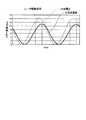
ところで、実際に光偏向器13の振幅制御を行う場合、起動直後はMEMSミラーとして構成される光偏向器13の振幅を急激に大きくすると主走査軸が破損する虞があるため、徐々に印加電圧を大きくして振幅量を調整していく。このとき、レーザ光源11から常にレーザ光が出射されている状態であると、上述の画像描画領域62に不要な画像が描画されてスクリーン40に投影される。これを回避するため、起動直後に光偏向器13の振幅調整を行う場合は、図5に示すように、光偏向器13の正弦波振幅の端部領域(主走査方向の端部となる領域)のみでレーザ光源11からレーザ光が出射されるように、光偏向器13の駆動に同期させてレーザ光源11にレーザ駆動信号を与えることが望ましい。実際には、図5に示すように、光偏向器13に対する印加電圧と光偏向器13の正弦波振幅との位相がずれているため、それに対応したタイミングでレーザ光源11にレーザ駆動信号を与える。一旦、光検出器14にレーザ光が入射して検知されれば、何らかの原因で光偏向器13の駆動感度が変動することがあっても、所定範囲内で駆動電圧を制御することで一定の振幅を維持することが可能である。 By the way, when the amplitude of theoptical deflector 13 is actually controlled, if the amplitude of theoptical deflector 13 configured as the MEMS mirror is suddenly increased immediately after the start-up, the main scanning axis may be damaged. Therefore, the applied voltage is gradually applied. Is increased to adjust the amount of amplitude. At this time, if the laser light is always emitted from thelaser light source 11, an unnecessary image is drawn in the above-mentionedimage drawing area 62 and projected on thescreen 40. In order to avoid this, when adjusting the amplitude of theoptical deflector 13 immediately after startup, as shown in FIG. 5, the end region of the sine wave amplitude of the optical deflector 13 (the region that becomes the end in the main scanning direction). It is desirable to give a laser drive signal to thelaser light source 11 in synchronization with the drive of thelight deflector 13 so that the laser light is emitted from thelaser light source 11 only by). Actually, as shown in FIG. 5, since the phase applied to theoptical deflector 13 and the sine wave amplitude of theoptical deflector 13 are out of phase, the laser drive signal is given to thelaser light source 11 at the corresponding timing. .. Once the laser beam is incident on thephotodetector 14 and detected, even if the drive sensitivity of thephotodetector 13 fluctuates for some reason, it is constant by controlling the drive voltage within a predetermined range. It is possible to maintain the amplitude.

以上、具体的な例を挙げながら説明したように、本実施形態によれば、被走査面上の光走査範囲60の少なくとも主走査方向の端部に検出領域61を有し、光走査範囲60内の画像描画領域62が、検出領域61に対して主走査方向に隣接する領域と、検出領域61に対して副走査方向に隣接する領域とを含む構成としているので、光走査範囲60における画像描画領域62の割合を大きくして、スクリーン40に表示される投影画像の画角を大きくすることができる。 As described above with reference to specific examples, according to the present embodiment, theoptical scanning range 60 has adetection region 61 at least at the end of theoptical scanning range 60 on the surface to be scanned in the main scanning direction. Since theimage drawing area 62 in theimage drawing area 62 includes an area adjacent to thedetection area 61 in the main scanning direction and an area adjacent to thedetection area 61 in the sub-scanning direction, the image in theoptical scanning range 60 The ratio of thedrawing area 62 can be increased to increase the angle of view of the projected image displayed on thescreen 40.

また、本実施形態によれば、画像描画領域62を検出領域61の位置を基準として複数の描画領域(メイン描画領域63およびサブ描画領域64)に分割し、それぞれの描画領域に種類の異なる画像を描画することにより、単純な矩形形状にならない画像描画領域62を有効に活用することができる。 Further, according to the present embodiment, theimage drawing area 62 is divided into a plurality of drawing areas (main drawing area 63 and sub drawing area 64) based on the position of thedetection area 61, and different types of images are provided in each drawing area. By drawing theimage drawing area 62, which does not have a simple rectangular shape, theimage drawing area 62 can be effectively utilized.

<第2の実施形態>
図6は、第2の実施形態に係るプロジェクタ装置100Bの概略構成を示す図である。本実施形態のプロジェクタ装置100Bは、上述の光走査装置10Aに代えて光走査装置10Bを備える点が、第1の実施形態のプロジェクタ装置100Aと異なる。光走査装置10Bは、上述の光走査装置10Aの光透過部材15に代えて中間スクリーン20が出射口に配置され、この中間スクリーン20が、レーザ光が走査される被走査面とされている。そして、光検出器14は中間スクリーン20に直接設けられず、中間スクリーン20に設けられた反射部により反射されたレーザ光を受光する位置に配置されている。その他の構成は第1の実施形態と同じであるため、以下では、同一もしくは対応する構成要素に対して共通の符号を付して重複した説明を適宜省略し、第1の実施形態との相違点のみ説明する。
<Second embodiment>
FIG. 6 is a diagram showing a schematic configuration of theprojector device 100B according to the second embodiment. Theprojector device 100B of the present embodiment is different from theprojector device 100A of the first embodiment in that it includes anoptical scanning device 10B instead of the above-mentioned optical scanning device 10A. In theoptical scanning device 10B, anintermediate screen 20 is arranged at the exit port instead of thelight transmitting member 15 of the optical scanning device 10A described above, and theintermediate screen 20 is used as a surface to be scanned on which the laser beam is scanned. Thephotodetector 14 is not directly provided on theintermediate screen 20, but is arranged at a position where the laser beam reflected by the reflecting portion provided on theintermediate screen 20 is received. Since the other configurations are the same as those of the first embodiment, the same or corresponding components are designated by a common reference numeral and duplicated description is appropriately omitted, and the differences from the first embodiment are omitted. Only the points will be explained.

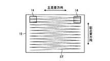
中間スクリーン20は、多数のマイクロレンズを主走査方向および副走査方向に配列したマイクロレンズアレイを有し、このマイクロレンズアレイによって二次元走査されるレーザ光の干渉による独特の輝度ムラ(スペックル)を抑制するものである。マイクロレンズアレイを構成する各マイクロレンズの曲率は、マイクロレンズとスクリーン40との間の光路長に基づいて設定されている。この中間スクリーン20は光走査装置10Bの出射口に配置され、レーザ光が走査される被走査面とされている。そして、この中間スクリーン20上の光走査範囲の少なくとも主走査方向の端部に、レーザ光を反射して光検出器14に入射させる反射部が設けられている。 Theintermediate screen 20 has a microlens array in which a large number of microlenses are arranged in the main scanning direction and the sub-scanning direction, and unique brightness unevenness (speckle) due to interference of laser light two-dimensionally scanned by the microlens array. It suppresses. The curvature of each microlens constituting the microlens array is set based on the optical path length between the microlens and thescreen 40. Theintermediate screen 20 is arranged at the exit port of theoptical scanning device 10B and is used as a surface to be scanned on which the laser beam is scanned. A reflecting portion that reflects the laser beam and causes it to enter thephotodetector 14 is provided at least at the end of the optical scanning range on theintermediate screen 20 in the main scanning direction.

図7は、中間スクリーン20の具体例を示す図である。中間スクリーン20には、レーザ光が走査される光走査範囲内に、主走査方向および副走査方向に配列された多数のマイクロレンズにより構成されるマイクロレンズアレイ21と、レーザ光を光検出器14に導くための反射部22とが設けられている。この図7に例示する中間スクリーン20では、被走査面上で二次元走査されるレーザ光を主走査方向の両端部および副走査方向の一方の端部で検出できるように、図の上側の主走査方向の両端部でレーザ光の軌跡STと重なる位置に、それぞれ反射部22が設けられている。この反射部22で反射されたレーザ光は、光検出器14に入射する。なお、光検出器14の直前に受光レンズを設けることで、レーザ光のビーム径を調節してもよい。 FIG. 7 is a diagram showing a specific example of theintermediate screen 20. Theintermediate screen 20 has amicrolens array 21 composed of a large number of microlenses arranged in the main scanning direction and the sub-scanning direction within the light scanning range in which the laser light is scanned, and thephotodetector 14 for the laser light. A reflectingportion 22 is provided to guide the light. In theintermediate screen 20 illustrated in FIG. 7, the laser beam scanned two-dimensionally on the surface to be scanned can be detected at both ends in the main scanning direction and one end in the sub-scanning direction. Reflectingportions 22 are provided at both ends in the scanning direction at positions that overlap with the laser beam locus ST. The laser beam reflected by the reflectingunit 22 is incident on thephotodetector 14. The beam diameter of the laser beam may be adjusted by providing a light receiving lens immediately before thephotodetector 14.

反射部22は、副走査方向に細長い主走査制御用反射部23と、主走査方向に細長い副走査制御用反射部24とを含む。本実施形態では、反射部22をこのように構成することによって、光偏向器13の振幅を主走査方向と副走査方向の双方において制御することができるようにしている。すなわち、コントローラ17は、主走査制御用反射部23で反射されたレーザ光を光検出器14が検出したタイミングに基づいて、光偏向器13の主走査方向の振幅を制御するとともに、副走査制御用反射部24で反射されたレーザ光を光検出器14が検出したタイミングに基づいて、光偏向器13の副走査方向の振幅を制御する。 The reflectingunit 22 includes a main scanningcontrol reflecting unit 23 elongated in the sub-scanning direction and a sub-scanningcontrol reflecting unit 24 elongated in the main scanning direction. In the present embodiment, the reflectingunit 22 is configured in this way so that the amplitude of thelight deflector 13 can be controlled in both the main scanning direction and the sub-scanning direction. That is, thecontroller 17 controls the amplitude of thelight deflector 13 in the main scanning direction based on the timing when thephotodetector 14 detects the laser beam reflected by the main scanningcontrol reflecting unit 23, and also controls the sub-scanning. The amplitude of thelight deflector 13 in the sub-scanning direction is controlled based on the timing at which thephotodetector 14 detects the laser beam reflected by thelight reflector 24.

図8は、中間スクリーン20と光検出器14との位置関係を説明する図であり、中間スクリーン20において二次元走査されるレーザ光の走査中心軸を上から垂直方向に見下ろした様子を示している。また、図9は、図8における中間スクリーン20の右側を拡大して示す図である。図8および図9に示すように、主走査制御用反射部23および副走査制御用反射部24は、中間スクリーン20の基板面に対して傾きを有しており、走査されたレーザ光の入射方向に対応してその反射方向が光検出器14に向かうようになっている。近年、マイクロレンズアレイ21は金型加工によって製造することができるようになっており、これら主走査制御用反射部23および副走査制御用反射部24を金型形状に反映しておくことで、一括で加工することも可能である。 FIG. 8 is a diagram for explaining the positional relationship between theintermediate screen 20 and thephotodetector 14, and shows a state in which the scanning central axis of the laser beam two-dimensionally scanned on theintermediate screen 20 is viewed from above in the vertical direction. There is. Further, FIG. 9 is an enlarged view showing the right side of theintermediate screen 20 in FIG. As shown in FIGS. 8 and 9, the main scanningcontrol reflecting unit 23 and the sub-scanningcontrol reflecting unit 24 are inclined with respect to the substrate surface of theintermediate screen 20, and the scanned laser beam is incident on them. The reflection direction corresponds to the direction toward thephotodetector 14. In recent years, themicrolens array 21 can be manufactured by die processing, and by reflecting these main scanningcontrol reflecting section 23 and sub-scanningcontrol reflecting section 24 in the mold shape, themicrolens array 21 can be manufactured. It is also possible to process all at once.

上述した第1の実施形態では、被走査面となる光透過部材15に光検出器14を直接配置し、光走査範囲60内の画像描画領域62を、光検出器14を配置した領域である検出領域61に対して主走査方向に隣接する領域と、検出領域61に対して副走査方向に隣接する領域とを含む構成とすることで、光走査範囲60における画像描画領域62の割合を大きくしていた。しかし、光検出器14は実際にはそれ自身のパッケージとしてのサイズがあり、電気信号を得るために回路基板に実装されているため、ある程度の大きさが必要である。このため、第1の実施形態のように光検出器14を被走査面に直接配置する構成では検出領域61のサイズが大きくなり、その分、画像描画領域62が小さくなる。 In the first embodiment described above, thephotodetector 14 is directly arranged on thelight transmitting member 15 to be the surface to be scanned, and theimage drawing area 62 within thelight scanning range 60 is the area where thephotodetector 14 is arranged. By including a region adjacent to thedetection region 61 in the main scanning direction and a region adjacent to thedetection region 61 in the sub-scanning direction, the ratio of theimage drawing region 62 in theoptical scanning range 60 is increased. Was. However, thephotodetector 14 actually has its own size as a package and is mounted on a circuit board in order to obtain an electric signal, so that a certain size is required. Therefore, in the configuration in which thephotodetector 14 is directly arranged on the surface to be scanned as in the first embodiment, the size of thedetection area 61 becomes large, and theimage drawing area 62 becomes small accordingly.

これに対し、本実施形態では、被走査面となる中間スクリーン20に光検出器14を配置せず、中間スクリーン20に設けた反射部22によって反射されたレーザ光が光検出器14に入射するようにしているので、光検出器14のパッケージサイズや回路基板の大きさの影響を受けることがなく、光走査範囲60における検出領域61のサイズを小さくして、画像描画領域62を広げることができる。 On the other hand, in the present embodiment, thephotodetector 14 is not arranged on theintermediate screen 20 which is the surface to be scanned, and the laser light reflected by the reflectingunit 22 provided on theintermediate screen 20 is incident on thephotodetector 14. Therefore, the size of thedetection area 61 in theoptical scanning range 60 can be reduced and theimage drawing area 62 can be expanded without being affected by the package size of thephotodetector 14 and the size of the circuit board. it can.

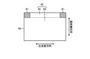
図10は、本実施形態における光走査範囲60のレイアウトを示す図である。図10に示すように、本実施形態においても、光走査範囲60の検出領域61を除いたすべての領域を、被走査面上を走査したレーザ光により画像を描画するための画像描画領域62としている。つまり、画像描画領域62が、検出領域61に対して主走査方向に隣接する領域と、検出領域61に対して副走査方向に隣接する領域とを含む構成としている。特に本実施形態では、図5に示した第1の実施形態の例と比較して、検出領域61のサイズを小さくすることができるので、その分、画像描画領域62を広げることができる。なお、本実施形態においても、画像描画領域62を検出領域61に対して副走査方向に隣接する領域を含むメイン描画領域63と、検出領域61に対して主走査方向に隣接する領域を含むサブ描画領域64とに分割し、それぞれの描画領域63,64に種類の異なる画像を描画することにより、単純な矩形形状にならない画像描画領域62を有効に活用することができる。 FIG. 10 is a diagram showing a layout of theoptical scanning range 60 in the present embodiment. As shown in FIG. 10, also in the present embodiment, all the regions except thedetection region 61 of theoptical scanning range 60 are used as theimage drawing region 62 for drawing an image by the laser beam scanned on the scanned surface. There is. That is, theimage drawing area 62 includes an area adjacent to thedetection area 61 in the main scanning direction and an area adjacent to thedetection area 61 in the sub-scanning direction. In particular, in the present embodiment, the size of thedetection area 61 can be reduced as compared with the example of the first embodiment shown in FIG. 5, so that theimage drawing area 62 can be expanded accordingly. Also in this embodiment, theimage drawing area 62 includes themain drawing area 63 including the area adjacent to thedetection area 61 in the sub-scanning direction, and the sub including the area adjacent to thedetection area 61 in the main scanning direction. By dividing the image into adrawing area 64 and drawing different types of images in thedrawing areas 63 and 64, theimage drawing area 62 that does not have a simple rectangular shape can be effectively used.

以上、具体的な例を挙げながら説明したように、本実施形態によれば、マイクロレンズアレイ21を有する中間スクリーン20を被走査面とし、この被走査面上を走査するレーザ光により描画される画像をスクリーン40に投影する構成としているので、レーザ光のスペックルを低減させた上で光利用効率を向上させ、スクリーン40に高画質の投影画像を表示することができる。 As described above with reference to specific examples, according to the present embodiment, theintermediate screen 20 having themicrolens array 21 is used as the surface to be scanned, and the image is drawn by the laser beam scanning on the surface to be scanned. Since the image is projected on thescreen 40, the speckle of the laser beam can be reduced, the light utilization efficiency can be improved, and a high-quality projected image can be displayed on thescreen 40.

また、本実施形態によれば、被走査面となる中間スクリーン20に反射部22を設け、この反射部22でレーザ光を反射して光検出器14に入射させる構成としているので、光走査範囲60における画像描画領域62の割合を第1の実施形態よりもさらに大きくして、スクリーン40に表示される投影画像の画角をさらに大きくすることができる。 Further, according to the present embodiment, the reflectingportion 22 is provided on theintermediate screen 20 to be the surface to be scanned, and the reflectingportion 22 reflects the laser beam to be incident on thephotodetector 14. Therefore, the optical scanning range. The ratio of theimage drawing area 62 in 60 can be further increased as compared with the first embodiment, and the angle of view of the projected image displayed on thescreen 40 can be further increased.

また、本実施形態によれば、反射部22が主走査制御用反射部23と副走査制御用反射部24とを含み、主走査制御用反射部23で反射されたレーザ光を光検出器14が検出したタイミングに基づいて光偏向器13の主走査方向の振幅を制御するとともに、副走査制御用反射部24で反射されたレーザ光を光検出器14が検出したタイミングに基づいて光偏向器13の副走査方向の振幅を制御するようにしているので、光偏向器13の主走査方向の振幅と副走査方向の振幅との双方を適切に制御することができる。 Further, according to the present embodiment, the reflectingunit 22 includes the main scanningcontrol reflecting unit 23 and the sub-scanningcontrol reflecting unit 24, and thephotodetector 14 detects the laser beam reflected by the main scanningcontrol reflecting unit 23. Controls the amplitude of thephotodetector 13 in the main scanning direction based on the timing detected by thephotodetector 13 and also controls the laser beam reflected by the sub-scanningcontrol reflecting unit 24 based on the timing detected by thephotodetector 14. Since the amplitude of the sub-scanning direction of the 13 is controlled, both the amplitude of thephotodetector 13 in the main scanning direction and the amplitude of the sub-scanning direction can be appropriately controlled.

(中間スクリーンの変形例)
ここで、上述した光走査装置10Bにおける中間スクリーン20の変形例について説明する。図7に例示した中間スクリーン20は、円形のマイクロレンズを主走査方向および副走査方向に配列したマイクロレンズアレイ21を備えているが、マイクロレンズアレイ21を構成する各マイクロレンズの形状は円形に限らない。例えば図11に示すように、中間スクリーン20のマイクロレンズアレイ21を、多角形のマイクロレンズを主走査方向および副走査方向に配列した構成としてもよい。マイクロレンズアレイ21を構成する各マイクロレンズアレイを図11のような多角形の形状とすることにより、各マイクロレンズ間の隙間を埋めることができる。
(Modified example of intermediate screen)
Here, a modified example of theintermediate screen 20 in the above-mentionedoptical scanning apparatus 10B will be described. Theintermediate screen 20 illustrated in FIG. 7 includes amicrolens array 21 in which circular microlenses are arranged in the main scanning direction and the sub-scanning direction, but the shape of each microlens constituting themicrolens array 21 is circular. Not exclusively. For example, as shown in FIG. 11, themicrolens array 21 of theintermediate screen 20 may be configured such that polygonal microlenses are arranged in the main scanning direction and the sub-scanning direction. By forming each microlens array constituting themicrolens array 21 into a polygonal shape as shown in FIG. 11, the gap between the microlenses can be filled.

また、中間スクリーン20のマイクロレンズアレイ21は、図12乃至図14に示すように、個々のマイクロレンズの中心が被走査面上におけるレーザ光の走査軌跡STと略一致するように各マイクロレンズを配列した構成としてもよい。具体的なマイクロレンズの配列の例としては、例えば、主走査方向の正弦波軌跡に対応して各マイクロレンズを配列することが考えられる。この場合、往路と走査線の画素に対応するマイクロレンズと復路の走査線の画素に対応するマイクロレンズとを水平方向に交互に配置することで、これらを分離するようになっている。 Further, in themicrolens array 21 of theintermediate screen 20, as shown in FIGS. 12 to 14, each microlens is arranged so that the center of each microlens substantially coincides with the scanning locus ST of the laser beam on the surface to be scanned. It may be an arranged configuration. As a specific example of the arrangement of microlenses, it is conceivable to arrange each microlens corresponding to the sinusoidal locus in the main scanning direction. In this case, the microlenses corresponding to the pixels of the outgoing and scanning lines and the microlenses corresponding to the pixels of the scanning lines of the returning path are alternately arranged in the horizontal direction to separate them.

正弦波軌跡の場合、光走査範囲の主走査方向の端部で走査が折り返すため、副走査方向に隣接する走査線ピッチが他の走査領域よりも密になる。そのため、同一サイズのマイクロレンズを同一ピッチで配列していくと、図12のような円形のマイクロレンズにより構成されるマイクロレンズアレイ21だけでなく、図13のような多角形のマイクロレンズで構成されるマイクロレンズアレイ21においても、主走査方向の端部でマイクロレンズアレイ間に隙間ができてしまう。そこで、図14に示すように、マイクロレンズアレイ21を構成するマイクロレンズの多角形の形状を、主走査方向の中央部と端部とで異なる形状とすることにより、マイクロレンズ間の隙間を埋める構成としてもよい。 In the case of a sinusoidal locus, the scanning is folded back at the end of the optical scanning range in the main scanning direction, so that the scanning line pitch adjacent to the sub-scanning direction is denser than the other scanning regions. Therefore, when microlenses of the same size are arranged at the same pitch, they are composed of not only themicrolens array 21 composed of circular microlenses as shown in FIG. 12 but also polygonal microlenses as shown in FIG. Also in themicrolens array 21 to be formed, a gap is formed between the microlens arrays at the end in the main scanning direction. Therefore, as shown in FIG. 14, the polygonal shape of the microlenses constituting themicrolens array 21 is different between the central portion and the end portion in the main scanning direction to fill the gap between the microlenses. It may be configured.

図12乃至図14に示す中間スクリーン20の変形例のように、マイクロレンズアレイ21を、個々のマイクロレンズの中心が被走査面上におけるレーザ光の走査軌跡STと略一致するように各マイクロレンズを配列した構成とすることで、レーザ光の走査軌跡STがマイクロレンズの配列に一致しないことに起因する画像の劣化を有効に抑制し、スクリーン40に表示される投影画像の画像品質および光利用効率をさらに向上させることができる。 As in the modification of theintermediate screen 20 shown in FIGS. 12 to 14, eachmicrolens array 21 is arranged so that the center of each microlens substantially coincides with the scanning locus ST of the laser beam on the surface to be scanned. By making the configuration in which the above are arranged, the deterioration of the image caused by the scanning locus ST of the laser beam not matching the arrangement of the microlens is effectively suppressed, and the image quality and light utilization of the projected image displayed on thescreen 40 are suppressed. The efficiency can be further improved.

また、図12乃至図14に示す中間スクリーン20の変形例では、反射部22の主走査制御用反射部23を、マイクロレンズアレイ21を構成するマイクロレンズの主走査方向の配列ピッチと略等しい間隔で設けられた複数の反射面23a,23bを含む構成とし、反射部22の副走査制御用反射部24を、マイクロレンズアレイ21を構成するマイクロレンズの副走査方向の配列ピッチと略等しい間隔で設けられた複数の反射面24a,24bを含む構成としている。 Further, in the modified example of theintermediate screen 20 shown in FIGS. 12 to 14, the distance between thereflection unit 23 for main scanning control of thereflection unit 22 is substantially equal to the arrangement pitch in the main scanning direction of the microlenses constituting themicrolens array 21. The reflectingunit 24 for sub-scanning control of the reflectingunit 22 is configured to include the plurality of reflectingsurfaces 23a and 23b provided in the above, at intervals substantially equal to the arrangement pitch in the sub-scanning direction of the microlenses constituting themicrolens array 21. The configuration includes a plurality of provided reflectingsurfaces 24a and 24b.

このように構成された中間スクリーン20を用いる場合、主走査制御用反射部23の一方の反射面23aで反射されたレーザ光を光検出器14が検出したタイミングと他方の反射面23aで反射されたレーザ光を光検出器14が検出したタイミングとに基づいて、レーザ光源11がレーザ光を出射するタイミングを制御することで、マイクロレンズそれぞれの位置に対応してレーザ光を発光させることができるので、スクリーン40に表示される投影画像の画質を向上させることができ、また、光利用効率を向上して明るい投影画像を表示することができる。 When theintermediate screen 20 configured in this way is used, the laser beam reflected by one of the reflectingsurfaces 23a of the main scanningcontrol reflecting unit 23 is reflected by the timing when thelight detector 14 detects it and the other reflectingsurface 23a. By controlling the timing at which thelaser light source 11 emits the laser light based on the timing at which thelight detector 14 detects the laser light, the laser light can be emitted corresponding to the position of each of the microlenses. Therefore, the image quality of the projected image displayed on thescreen 40 can be improved, and the light utilization efficiency can be improved to display a bright projected image.

また、副走査制御用反射部24の一方の反射面24aで反射されたレーザ光を光検出器14が検出したタイミングと他方の反射面24aで反射されたレーザ光を光検出器14が検出したタイミングとに基づいて、光偏向器13に印加する副走査方向の駆動電圧のバイアス値を制御することによって、マイクロレンズそれぞれの位置に対応するようにレーザ光の走査軌跡STを調整することができるので、スクリーン40に表示される投影画像の画質を向上させることができ、また、光利用効率を向上して明るい投影画像を表示することができる。 Further, thephotodetector 14 detects the timing at which thephotodetector 14 detects the laser light reflected by one of the reflectingsurfaces 24a of the sub-scanningcontrol reflecting unit 24 and the laser light reflected by the other reflectingsurface 24a. By controlling the bias value of the drive voltage in the sub-scanning direction applied to thephotodetector 13 based on the timing, the scanning locus ST of the laser beam can be adjusted so as to correspond to the position of each microlens. Therefore, the image quality of the projected image displayed on thescreen 40 can be improved, and the light utilization efficiency can be improved to display a bright projected image.

なお、主走査制御用反射部23の反射面23a,23bや副走査制御用反射部24の反射面24a,24bをマイクロレンズの配列ピッチと略等しい間隔で設けると各反射面の面積が小さくなりすぎて、光検出器14に適切にレーザ光を導くことが困難になる場合がある。このような場合には、反射面23a,23bの間隔や反射面24a,24bの間隔をマイクロレンズの配列ピッチよりも大きくし、その比率に応じて光検出器14がレーザ光を検出したタイミングを補正した上で、上記のような制御を行うようにしてもよい。 If the reflectingsurfaces 23a and 23b of the main scanningcontrol reflecting unit 23 and the reflectingsurfaces 24a and 24b of the sub-scanningcontrol reflecting unit 24 are provided at intervals substantially equal to the arrangement pitch of the microlenses, the area of each reflecting surface becomes smaller. Too much, it may be difficult to properly guide the laser beam to thephotodetector 14. In such a case, the distance between the reflectingsurfaces 23a and 23b and the distance between the reflectingsurfaces 24a and 24b are made larger than the arrangement pitch of the microlenses, and the timing at which thephotodetector 14 detects the laser beam is determined according to the ratio. After the correction, the above-mentioned control may be performed.

(レーザ光源および光偏向器の変形例)
次に、上述した光検出器10Bにおけるレーザ光源11および光偏向器13の変形例について説明する。レーザ光源11および光偏向器13は、例えば図15に示すような光学ユニット80として一体に構成してもよい。図15は、レーザ光源11および光偏向器13を含む光学ユニット80の一例を示す図であり、RGBの3色のレーザ光を合成して中間スクリーン20上を走査することで、カラー画像を描画できるように構成したものである。
(Variation example of laser light source and light deflector)
Next, a modification of thelaser light source 11 and thelight deflector 13 in the above-mentionedphotodetector 10B will be described. Thelaser light source 11 and thelight deflector 13 may be integrally configured as, for example, anoptical unit 80 as shown in FIG. FIG. 15 is a diagram showing an example of anoptical unit 80 including alaser light source 11 and anoptical deflector 13, and draws a color image by synthesizing laser beams of three colors of RGB and scanning on theintermediate screen 20. It is configured so that it can be done.

図15に例示する光学ユニット80では、RGBの3色のレーザ光を出射するレーザ光源11と光偏向器13とが、筐体81により支持されている。筐体81内の3つのレーザ光源11の出射端近傍には、各レーザ光源11からの発散光を略平行光にするコリメートレンズ12が配置されている。また、筐体81内には、3色のレーザ光を合成する合成プリズム82が配置されている。各レーザ光源11から出射されコリメートレンズ12により略平行光となった3色のレーザ光は、合成プリズム82により合成され、光偏向器13に入射する。光偏向器13は、合成された3色のレーザ光を被走査面である中間スクリーン20上で二次元方向に走査させ、中間スクリーン20上にカラー画像を描画する。このカラー画像がスクリーン40に投影されることで、スクリーン40にカラーの投影画像を表示することができる。 In theoptical unit 80 illustrated in FIG. 15, alaser light source 11 and anoptical deflector 13 that emit laser beams of three colors of RGB are supported by ahousing 81. In the vicinity of the emission ends of the threelaser light sources 11 in thehousing 81,collimating lenses 12 that make the divergent light from eachlaser light source 11 substantially parallel light are arranged. Further, asynthetic prism 82 that synthesizes laser beams of three colors is arranged in thehousing 81. The three-color laser light emitted from eachlaser light source 11 and becoming substantially parallel light by the collimatedlens 12 is combined by thesynthetic prism 82 and incident on thelight deflector 13. Thelight deflector 13 scans the combined three-color laser light in the two-dimensional direction on theintermediate screen 20 which is the surface to be scanned, and draws a color image on theintermediate screen 20. By projecting this color image on thescreen 40, the color projected image can be displayed on thescreen 40.

<第3の実施形態>
上述した第1の実施形態および第2の実施形態ではプロジェクタ装置100A,100Bへの適用例を説明したが、本実施形態ではヘッドアップディスプレイ装置への適用例を説明する。
<Third embodiment>
In the first embodiment and the second embodiment described above, an example of application to theprojector devices 100A and 100B has been described, but in this embodiment, an example of application to the head-up display device will be described.

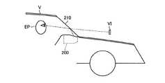
図16は、第3の実施形態に係るヘッドアップディスプレイ装置200の概略構成を示す図であり、図17は、ヘッドアップディスプレイ装置200を搭載した車両Vの概念図である。図16および図17に例示する本実施形態のヘッドアップディスプレイ装置200は、車両Vのフロントガラス210を投射面の一部として使用したウィンドウシールド方式のヘッドアップディスプレイ装置である。 FIG. 16 is a diagram showing a schematic configuration of the head-updisplay device 200 according to the third embodiment, and FIG. 17 is a conceptual diagram of a vehicle V equipped with the head-updisplay device 200. The head-updisplay device 200 of the present embodiment illustrated in FIGS. 16 and 17 is a window shield type head-up display device using thewindshield 210 of the vehicle V as a part of the projection surface.

このヘッドアップディスプレイ装置200は、図16に示すように、筐体201内のベース202上に防振材203を介して光走査装置10Cを配置し、光走査装置10Cにより描画される画像を、投影ミラー204で反射させて出射窓部205を介してフロントガラス210に投射する構成である。このヘッドアップディスプレイ装置200は、図17に示すように、光走査装置10Cにより描画される画像を、車両Vのドライバの視点位置EP(観察位置)前方のフロントガラス210(ガラス部材)に投射することにより、ドライバの視点位置EPからフロントガラス210を介して、光走査装置10Cにより描画される画像の虚像VIを視認可能にしている。すなわち、光走査装置10Cにより描画される画像がフロントガラス210で反射されてドライバの視点位置EPに届くことにより、ドライバの視点位置EPからは、この画像の虚像VIがフロントガラス210の数m先のスクリーンに投影された画像として認識される。 As shown in FIG. 16, the head-updisplay device 200 arranges the optical scanning device 10C on the base 202 in thehousing 201 via theanti-vibration material 203, and displays an image drawn by the optical scanning device 10C. It is configured to be reflected by theprojection mirror 204 and projected onto thewindshield 210 through theexit window portion 205. As shown in FIG. 17, the head-updisplay device 200 projects an image drawn by the optical scanning device 10C onto a windshield 210 (glass member) in front of the viewpoint position EP (observation position) of the driver of the vehicle V. As a result, the virtual image VI of the image drawn by the optical scanning device 10C can be visually recognized from the viewpoint position EP of the driver via thewindshield 210. That is, the image drawn by the optical scanning device 10C is reflected by thewindshield 210 and reaches the driver's viewpoint position EP, so that the virtual image VI of this image is several meters ahead of thewindshield 210 from the driver's viewpoint position EP. It is recognized as an image projected on the screen of.

図18は、本実施形態のヘッドアップディスプレイ装置200が備える光走査装置10Cの概略構成を示す図である。光走査装置10Cの基本的な構成は上述の第2の実施形態の光走査装置10Bと同様であり、マイクロレンズアレイ21および反射部22を有する中間スクリーン20を被走査面としている。ただし、本実施形態の光走査装置10Cは、車両Vの限られた空間に適切に搭載できるように、光偏向器13により偏向走査するレーザ光をミラー90により折り返して中間スクリーン20に照射する構成とすることで、サイズをコンパクト化している。 FIG. 18 is a diagram showing a schematic configuration of an optical scanning device 10C included in the head-updisplay device 200 of the present embodiment. The basic configuration of the optical scanning device 10C is the same as that of theoptical scanning device 10B of the second embodiment described above, and theintermediate screen 20 having themicrolens array 21 and the reflectingportion 22 is used as the surface to be scanned. However, the optical scanning device 10C of the present embodiment has a configuration in which the laser beam deflected and scanned by theoptical deflector 13 is folded back by the mirror 90 and irradiated to theintermediate screen 20 so that it can be appropriately mounted in the limited space of the vehicle V. By doing so, the size is made compact.

本実施形態の光走査装置10Cにおいても、第2の実施形態の光走査装置10Bと同様に、レーザ光源11から出射したレーザ光が光偏向器13により中間スクリーン20上で主走査方向および副走査方向の二次元方向に走査される。そして、中間スクリーン20上の光走査範囲60の少なくとも主走査方向の端部において、レーザ光が反射部22により反射されて光検出器14に入射することで、被走査面上を走査したレーザ光を光検出器14で検出できるようにしている。また、画像情報に応じて変調されたレーザ光により中間スクリーン20上を走査することで、中間スクリーン20上に画像情報に応じた画像が描画され、この画像が車両Vのフロントガラス210に投射される。なお、図18ではレーザ光源11を1つのみ図示しているが、図15に示した光学ユニット80のようにRGB3色のレーザ光源11を備える構成とすることで、中間スクリーン20にカラー画像を描画して車両Vのフロントガラス210に投射することもできる。 In the optical scanning device 10C of the present embodiment as well, similarly to theoptical scanning device 10B of the second embodiment, the laser light emitted from thelaser light source 11 is subjected to the main scanning direction and the sub-scanning on theintermediate screen 20 by theoptical deflector 13. It is scanned in the two-dimensional direction of the direction. Then, at least at the end of thelight scanning range 60 on theintermediate screen 20 in the main scanning direction, the laser light is reflected by the reflectingunit 22 and incident on thephotodetector 14, so that the laser light scanned on the scanned surface. Can be detected by thephotodetector 14. Further, by scanning on theintermediate screen 20 with the laser beam modulated according to the image information, an image corresponding to the image information is drawn on theintermediate screen 20, and this image is projected onto thewindshield 210 of the vehicle V. To. Although only onelaser light source 11 is shown in FIG. 18, a color image can be displayed on theintermediate screen 20 by providing thelaser light source 11 of three RGB colors as in theoptical unit 80 shown in FIG. It can also be drawn and projected onto thewindshield 210 of the vehicle V.

図19乃至図21は、中間スクリーン20に描画されて車両Vのフロントガラス210に投射される画像の一例を示す図である。 19 to 21 are views showing an example of an image drawn on theintermediate screen 20 and projected on thewindshield 210 of the vehicle V.

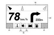
図19に示す例では、光走査範囲60の上側左右両端部を検出領域61とし、それ以外の領域を画像描画領域62としている。そして、検出領域61の位置を基準として画像描画領域62を大サイズのメイン描画領域63と小サイズのサブ描画領域64とに分割し、メイン描画領域63にスピードメータとナビゲーション画面、サブ描画領域64に警告灯を描画する構成としている。このように、検出領域61の位置を基準として画像描画領域62をメイン描画領域63とサブ描画領域64とに分割し、それぞれの領域に適した画像を描画することで、画像描画領域62の形状が単純な矩形でなくとも画像描画領域62を有効利用して適切な画像を車両Vのフロントガラス210に投射することができる。 In the example shown in FIG. 19, the upper left and right ends of theoptical scanning range 60 are designated as thedetection region 61, and the other regions are designated as theimage drawing region 62. Then, theimage drawing area 62 is divided into a large-sizedmain drawing area 63 and a small-sizedsub-drawing area 64 based on the position of thedetection area 61, and the speedometer, the navigation screen, and thesub-drawing area 64 are divided into themain drawing area 63. A warning light is drawn on the screen. In this way, theimage drawing area 62 is divided into amain drawing area 63 and asub drawing area 64 based on the position of thedetection area 61, and an image suitable for each area is drawn to form the shape of theimage drawing area 62. Is not a simple rectangle, but theimage drawing area 62 can be effectively used to project an appropriate image onto thewindshield 210 of the vehicle V.

図20に示す例では、光走査範囲60の下側左右両端部を検出領域61とし、それ以外の領域を画像描画領域62としている。そして、検出領域61の位置を基準として画像描画領域62を大サイズのメイン描画領域63と小サイズのサブ描画領域64とに分割し、メイン描画領域63にAR(拡張現実)画像、スピードメータ、およびナビゲーション画面を描画し、サブ描画領域64に警告灯を描画する構成としている。また、図21に示す例では、光走査範囲60の垂直方向の中央部の左右両端部を検出領域61とし、それ以外の領域を画像描画領域62としている。そして、検出領域61の位置を基準として画像描画領域62を大サイズのメイン描画領域63と小サイズのサブ描画領域64とに分割し、メイン描画領域63にスピードメータ、ナビゲーション画面、および警告灯を描画し、サブ描画領域64にAR画像を描画する構成としている。 In the example shown in FIG. 20, the lower left and right ends of theoptical scanning range 60 are designated as thedetection region 61, and the other regions are designated as theimage drawing region 62. Then, theimage drawing area 62 is divided into a large-sizedmain drawing area 63 and a small-sizedsub-drawing area 64 based on the position of thedetection area 61, and the AR (augmented reality) image, the speedometer, and themain drawing area 63 are divided into themain drawing area 63. And the navigation screen is drawn, and the warning light is drawn in thesub drawing area 64. Further, in the example shown in FIG. 21, the left and right ends of the central portion of theoptical scanning range 60 in the vertical direction are designated as thedetection region 61, and the other regions are designated as theimage drawing region 62. Then, theimage drawing area 62 is divided into a large-sizedmain drawing area 63 and a small-sizedsub-drawing area 64 based on the position of thedetection area 61, and a speedometer, a navigation screen, and a warning light are provided in themain drawing area 63. It is configured to draw and draw an AR image in thesub drawing area 64.

近年、車両Vに搭載するヘッドアップディスプレイ装置200においても拡張現実(AR:Augmented Reality)が応用されてきており、具体例として、例えば衝突安全を目的とした前方検知に関連する内容をAR画像として表示するものがある。このようなAR画像を適切に表示するために、画像描画領域62の上側は水平方向に広い領域をAR画像を描画するための領域65として確保したいという要求がある。図20に示す例や図21に示す例では、光走査範囲60の下側左右両端部や中央部の左右両端部を検出領域61としているので、光走査範囲60の上側にAR画像の描画に適した水平方向に広い領域65を確保することができる。 In recent years, augmented reality (AR) has also been applied to the head-updisplay device 200 mounted on the vehicle V, and as a specific example, for example, content related to forward detection for the purpose of collision safety is used as an AR image. There is something to display. In order to properly display such an AR image, there is a demand that a wide area in the horizontal direction is secured as anarea 65 for drawing an AR image on the upper side of theimage drawing area 62. In the example shown in FIG. 20 and the example shown in FIG. 21, since the lower left and right ends of theoptical scanning range 60 and the left and right ends of the central portion are thedetection areas 61, the AR image can be drawn on the upper side of theoptical scanning range 60. A suitable horizontalwide area 65 can be secured.

以上、具体的な例を挙げながら説明したように、本実施形態のヘッドアップディスプレイ装置200によれば、上述した第2の実施形態のプロジェクタ装置100Bと同様に、光走査範囲60における画像描画領域62の割合を大きくすることができ、車両Vのフロントガラス210に投射する画像の画角を大きくすることができる。また、マイクロレンズアレイ21を有する中間スクリーン20を被走査面とし、この被走査面上を走査するレーザ光により描画される画像を車両Vのフロントガラス210に投射する構成としているので、レーザ光のスペックルを低減させた上で光利用効率を向上させ、車両Vのフロントガラス210に高画質の画像を投射することができる。 As described above with reference to specific examples, according to the head-updisplay device 200 of the present embodiment, the image drawing area in theoptical scanning range 60 is similar to theprojector device 100B of the second embodiment described above. The ratio of 62 can be increased, and the angle of view of the image projected on thewindshield 210 of the vehicle V can be increased. Further, since theintermediate screen 20 having themicrolens array 21 is used as the surface to be scanned and the image drawn by the laser light scanning on the surface to be scanned is projected onto thewindshield 210 of the vehicle V, the laser light can be used. It is possible to reduce the speckle, improve the light utilization efficiency, and project a high-quality image on thewindshield 210 of the vehicle V.

以上、本発明の具体的な実施形態について説明したが、上述した実施形態は本発明の一適用例を示したものである。本発明は、上述した実施形態そのままに限定されるものではなく、実施段階ではその要旨を逸脱しない範囲で様々な変形や変更を加えて具体化することができる。 Although the specific embodiment of the present invention has been described above, the above-described embodiment shows an application example of the present invention. The present invention is not limited to the above-described embodiment as it is, and can be embodied by making various modifications and changes at the implementation stage without departing from the gist thereof.

10A,10B,10C 光走査装置
11 レーザ光源
13 光偏向器
14 光検出器
17 コントローラ
20 中間スクリーン
21 マイクロレンズアレイ
22 反射部
23 主走査制御用反射部
24 副走査制御用反射部
60 光走査範囲
61 検出領域
62 画像描画領域
63 メイン描画領域
64 サブ描画領域
100A,100B プロジェクタ装置
200 ヘッドアップディスプレイ装置
210 フロントガラス
10A, 10B, 10COptical scanning device 11 Laserlight source 13Optical deflector 14Optical detector 17Controller 20Intermediate screen 21Microlens array 22Reflector 23 Reflector formain scanning control 24 Reflector forsecondary scanning control 60Optical scanning range 61Detection area 62Image drawing area 63Main drawing area 64Sub drawing area 100A,100B Projector device 200 Head-updisplay device 210 Front glass

特開2015−49266号公報JP-A-2015-49266特開2015−148654号公報JP 2015-148654

Claims (7)

Translated fromJapanese
光源と、Light source and
前記光源からの光を偏向して被走査面上で主走査方向および副走査方向に走査させる光偏向器と、An optical deflector that deflects the light from the light source to scan in the main scanning direction and the sub-scanning direction on the surface to be scanned, and
前記被走査面上を走査した光を検出する光検出器と、A photodetector that detects the light scanned on the surface to be scanned, and
前記光検出器が光を検出したタイミングに基づいて、前記光源の動作と前記光偏向器の動作との少なくとも一方を制御するコントローラと、を備え、A controller that controls at least one of the operation of the light source and the operation of the light deflector based on the timing at which the photodetector detects light is provided.
前記被走査面上の光が走査される範囲である光走査範囲の少なくとも主走査方向の端部に、前記光検出器により光を検出するための検出領域を有し、前記光走査範囲内の画像描画に用いる画像描画領域が、前記検出領域に対して主走査方向に隣接する領域と、前記検出領域に対して副走査方向に隣接する領域とを含み、A detection region for detecting light by the photodetector is provided at least at the end of the optical scanning range, which is a range in which light is scanned on the surface to be scanned, in the main scanning direction, and is within the optical scanning range. The image drawing area used for image drawing includes an area adjacent to the detection area in the main scanning direction and an area adjacent to the detection area in the sub-scanning direction.
前記被走査面は、マイクロレンズアレイを有する中間スクリーンであり、The surface to be scanned is an intermediate screen having a microlens array.
前記中間スクリーン上の前記光走査範囲の少なくとも主走査方向の端部に、光を反射して前記光検出器に入射させる反射部が設けられ、A reflecting portion that reflects light and causes it to enter the photodetector is provided at least at the end of the optical scanning range on the intermediate screen in the main scanning direction.
前記検出領域は、前記反射部が設けられた前記中間スクリーン上の領域であり、The detection area is an area on the intermediate screen provided with the reflection portion, and is an area on the intermediate screen.
前記反射部は、前記マイクロレンズアレイを構成するマイクロレンズの配列ピッチと略等しい間隔で設けられた複数の反射面を含むことThe reflecting unit includes a plurality of reflecting surfaces provided at intervals substantially equal to the arrangement pitch of the microlenses constituting the microlens array.
を特徴とする光走査装置。An optical scanning device characterized by.
前記検出領域に対して主走査方向に隣接する第1の画像描画領域と前記検出領域に対して副走査方向に隣接する第2の画像描画領域とは、前記検出領域の位置を基準として、互いに異なる種類の画像を描画するための複数の描画領域に分割され、
前記第1の画像描画領域の面積は、前記第2の画像描画領域の面積よりも小さいこと
を特徴とする請求項1に記載の光走査装置。
The first image drawing areaadjacent to the detection area in the main scanning direction andthe second image drawing area adjacent to the detection area in the sub-scanning direction are relative to each other with reference to the position of the detection area. Divided into multiple drawing areas for drawing different types of images,
The optical scanning apparatus accordingto claim 1 , wherein the area of the first image drawing area is smaller than the area of the second image drawing area.
前記コントローラは、前記反射部の複数の反射面の1つで反射された光を前記光検出器が検出したタイミングと、前記反射部の複数の反射面の他の1つで反射された光を前記光検出器が検出したタイミングとに基づいて、前記光源の発光タイミングを制御すること
を特徴とする請求項1または2に記載の光走査装置。
The controller sets the timing at which the light detector detects the light reflected by one of the plurality of reflecting surfaces of the reflecting portion and the light reflected by the other one of the plurality of reflecting surfaces of the reflecting portion. The optical scanning apparatus accordingto claim 1 or 2 , wherein the light emission timing of the light source is controlled based on the timing detected by the optical detector.
前記マイクロレンズアレイは、個々のマイクロレンズの中心が前記被走査面上で走査される光の軌跡と略一致するように各マイクロレンズを配列した構成であること
を特徴とする請求項乃至のいずれか一項に記載の光走査装置。
Claims 1 to3 are characterized in that the microlens array has a configuration in which each microlens is arranged so that the center of each microlens substantially coincides with the locus of light scanned on the scanned surface. The optical scanning apparatus according to any one of the above.
前記反射部は、主走査制御用反射部と副走査制御用反射部とを含み、
前記コントローラは、前記主走査制御用反射部で反射された光を前記光検出器が検出したタイミングに基づいて、前記光偏向器の主走査方向の振幅を制御するとともに、前記副走査制御用反射部で反射された光を前記光検出器が検出したタイミングに基づいて、前記光偏向器の副走査方向の振幅を制御すること
を特徴とする請求項乃至のいずれか一項に記載の光走査装置。
The reflection unit includes a reflection unit for main scanning control and a reflection unit for sub-scanning control.
The controller controls the amplitude of the light deflector in the main scanning direction based on the timing when the photodetector detects the light reflected by the main scanning control reflecting unit, and also controls the sub-scanning control reflection. The invention according to any one ofclaims 1 to4 , wherein the amplitude of the photodetector in the sub-scanning direction is controlled based on the timing at which the light reflected by the unit is detected by the photodetector. Optical scanning device.
請求項1乃至のいずれか一項に記載の光走査装置を備え、
前記被走査面上の前記画像描画領域を走査する光により描画される画像をスクリーンに投影して表示するプロジェクタ装置。
The optical scanning apparatus according to any one of claims 1 to5 is provided.
A projector device that projects and displays an image drawn by light scanning the image drawing area on the scanned surface onto a screen.
請求項1乃至のいずれか一項に記載の光走査装置を備え、
前記被走査面上の前記画像描画領域を走査する光により描画される画像を観察位置の前方のガラス部材に投射して、前記観察位置から前記ガラス部材を介して前記画像の虚像を視認可能にするヘッドアップディスプレイ装置。
The optical scanning apparatus according to any one of claims 1 to5 is provided.
An image drawn by light scanning the image drawing area on the scanned surface is projected onto a glass member in front of the observation position so that a virtual image of the image can be visually recognized from the observation position via the glass member. Head-up display device.
JP2016132794A2016-07-042016-07-04 Optical scanning device, projector device and head-up display deviceActiveJP6903875B2 (en)

Priority Applications (2)

Application NumberPriority DateFiling DateTitle
JP2016132794AJP6903875B2 (en)2016-07-042016-07-04 Optical scanning device, projector device and head-up display device
EP17178567.8AEP3267236B1 (en)2016-07-042017-06-29Optical scanner, projector, and heads-up display

Applications Claiming Priority (1)

Application NumberPriority DateFiling DateTitle
JP2016132794AJP6903875B2 (en)2016-07-042016-07-04 Optical scanning device, projector device and head-up display device

Publications (2)

Publication NumberPublication Date
JP2018005007A JP2018005007A (en)2018-01-11
JP6903875B2true JP6903875B2 (en)2021-07-14

Family

ID=59258035

Family Applications (1)

Application NumberTitlePriority DateFiling Date
JP2016132794AActiveJP6903875B2 (en)2016-07-042016-07-04 Optical scanning device, projector device and head-up display device

Country Status (2)

CountryLink
EP (1)EP3267236B1 (en)
JP (1)JP6903875B2 (en)

Families Citing this family (13)

* Cited by examiner, † Cited by third party
Publication numberPriority datePublication dateAssigneeTitle
CN110068925B (en)*2018-01-232022-12-06松下知识产权经营株式会社Image display device
JP7018565B2 (en)*2018-02-022022-02-14パナソニックIpマネジメント株式会社 Image display device
US10795154B2 (en)*2018-02-232020-10-06Denso International America, Inc.Head-up display
US10948776B2 (en)2018-02-232021-03-16Denso International America, Inc.Head-up display
JP2019164247A (en)*2018-03-192019-09-26株式会社リコーOptical scan device, image display device, and moving body
JP2020122858A (en)2019-01-302020-08-13株式会社リコーOptical scanner, display system and moving body
JP2020144326A (en)2019-03-082020-09-10株式会社リコーOptical scanner, display system, and movable body
JP2020148976A (en)*2019-03-152020-09-17株式会社リコー Optical scanning devices, display systems and moving objects
JP2020154111A (en)*2019-03-202020-09-24株式会社リコー Optical scanning devices, display systems, and moving objects
JP2020194122A (en)2019-05-292020-12-03株式会社リコー Optical scanners, display systems, and mobiles
JP2021081568A (en)*2019-11-192021-05-27株式会社リコーOptical element, display unit, display system, and movable body
DE102021130561A1 (en)2021-11-232023-05-25Carl Zeiss Jena Gmbh PROJECTOR OR DISPLAY WITH SCANNING LIGHT SOURCE AND PIXELATED ARRAY
US12366699B2 (en)2022-03-162025-07-22Google LlcCoupling narrowband projector source light into display waveguides

Family Cites Families (14)

* Cited by examiner, † Cited by third party
Publication numberPriority datePublication dateAssigneeTitle
JP4620901B2 (en)*2001-06-042011-01-26キヤノン株式会社 Two-dimensional optical scanning device and method for driving the two-dimensional optical scanning device
GB2429075A (en)*2005-08-102007-02-14Thales Holdings Uk PlcApparatus and method of projection control
US7954953B2 (en)*2008-07-302011-06-07Microvision, Inc.Scanned beam overlay projection
JP2010145924A (en)*2008-12-222010-07-01Equos Research Co LtdImage forming apparatus and head-up display device
JP2010145922A (en)*2008-12-222010-07-01Equos Research Co LtdImage forming apparatus and head-up display device
WO2013179493A1 (en)*2012-06-012013-12-05パイオニア株式会社Image projection apparatus, headup display, control method, and optical element
CN103868675B (en)*2012-12-132016-08-17光宝科技股份有限公司 Laser projector and its detection method for scanning angle range of laser beam
US9158124B2 (en)*2012-12-212015-10-13Ricoh Company, Ltd.Image display device and vehicle incorporating the same
JP6107185B2 (en)*2013-02-052017-04-05株式会社リコー Image forming apparatus and image display apparatus
JP6387589B2 (en)2013-08-302018-09-12株式会社リコー Image forming apparatus, vehicle, and control method of image forming apparatus
JP6278180B2 (en)2014-02-052018-02-14株式会社リコー Optical scanning device, image display device, and moving body
JP6332736B2 (en)*2014-02-252018-05-30株式会社リコー Tilt operation device, optical scanning device and image display device using the same
JP6269463B2 (en)*2014-03-282018-01-31株式会社Jvcケンウッド Image display device and image display adjustment method
JP6455802B2 (en)*2014-12-082019-01-23株式会社リコー Image display device, object device, transmission screen and screen

Also Published As

Publication numberPublication date
JP2018005007A (en)2018-01-11
EP3267236B1 (en)2021-03-10
EP3267236A1 (en)2018-01-10

Similar Documents

PublicationPublication DateTitle
JP6903875B2 (en) Optical scanning device, projector device and head-up display device
US10573213B2 (en)Image display apparatus and vehicle
JP4522253B2 (en) Optical scanning device and image display device using the same
JP6891402B2 (en) Adjustment method of light deflector, image forming device, image display device, object device, and light deflector
US7576315B2 (en)Scanning type image display apparatus having a synchronization control circuit and a light transmitting area on the last surface of a scanning optical system
US20190236762A1 (en)Device and Method for Projecting an Image
US20060007362A1 (en)Apparatus for and method of scaling a scanning angle and image projection apparatus incorporating the same
JP6627886B2 (en) Optical scanning device, image display device, and vehicle
JP2019534467A (en) Apparatus and method for providing depth mapping along with scanning of laser image projection
JP6735023B2 (en) Display image creation device and image display device
JP6485013B2 (en) Optical deflector, image display device, and object device
JP6278180B2 (en) Optical scanning device, image display device, and moving body
JP2012145755A (en)Image display device
US11624903B2 (en)Light deflector, LiDAR device, and image forming apparatus
US20210132385A1 (en)Movable device, image projection apparatus, head-up display, laser headlamp, head-mounted display, object recognition device, and vehicle
JP4620905B2 (en) Two-dimensional optical scanning device
JP2023158162A (en) Optical scanning device, optical scanning method and program
JP6555568B2 (en) Image display device
JP2022107261A (en) Light deflector and image projection device
JP2021085983A (en)Optical deflector, deflecting device, distance measuring device, image projection device, and vehicle
JP2010266824A (en) Image display device
JP2007140009A (en) Image display device
JP2020194116A (en)Laser scanning type video device
JP7036158B2 (en) Display image creation device and image display device
JP2021071582A (en)Light deflector, image projection device, head-up display, laser head lamp, head-mounted display, object recognition device, and vehicle

Legal Events

DateCodeTitleDescription
A621Written request for application examination

Free format text:JAPANESE INTERMEDIATE CODE: A621

Effective date:20190522

A977Report on retrieval

Free format text:JAPANESE INTERMEDIATE CODE: A971007

Effective date:20200313

A131Notification of reasons for refusal

Free format text:JAPANESE INTERMEDIATE CODE: A131

Effective date:20200324

A521Request for written amendment filed

Free format text:JAPANESE INTERMEDIATE CODE: A523

Effective date:20200522

A131Notification of reasons for refusal

Free format text:JAPANESE INTERMEDIATE CODE: A131

Effective date:20201013

A521Request for written amendment filed

Free format text:JAPANESE INTERMEDIATE CODE: A523

Effective date:20201214

TRDDDecision of grant or rejection written
A01Written decision to grant a patent or to grant a registration (utility model)

Free format text:JAPANESE INTERMEDIATE CODE: A01

Effective date:20210525

A61First payment of annual fees (during grant procedure)

Free format text:JAPANESE INTERMEDIATE CODE: A61

Effective date:20210607

R151Written notification of patent or utility model registration

Ref document number:6903875

Country of ref document:JP

Free format text:JAPANESE INTERMEDIATE CODE: R151


[8]ページ先頭

©2009-2025 Movatter.jp