JP6903362B1 - Method for manufacturing crystals for synthetic gemstones - Google Patents
Method for manufacturing crystals for synthetic gemstonesDownload PDFInfo
- Publication number
- JP6903362B1 JP6903362B1JP2021017259AJP2021017259AJP6903362B1JP 6903362 B1JP6903362 B1JP 6903362B1JP 2021017259 AJP2021017259 AJP 2021017259AJP 2021017259 AJP2021017259 AJP 2021017259AJP 6903362 B1JP6903362 B1JP 6903362B1
- Authority
- JP
- Japan
- Prior art keywords
- single crystal
- sic single
- density
- electron beam
- irradiation
- Prior art date
- Legal status (The legal status is an assumption and is not a legal conclusion. Google has not performed a legal analysis and makes no representation as to the accuracy of the status listed.)
- Active
Links
Images


Classifications
- C—CHEMISTRY; METALLURGY
- C30—CRYSTAL GROWTH
- C30B—SINGLE-CRYSTAL GROWTH; UNIDIRECTIONAL SOLIDIFICATION OF EUTECTIC MATERIAL OR UNIDIRECTIONAL DEMIXING OF EUTECTOID MATERIAL; REFINING BY ZONE-MELTING OF MATERIAL; PRODUCTION OF A HOMOGENEOUS POLYCRYSTALLINE MATERIAL WITH DEFINED STRUCTURE; SINGLE CRYSTALS OR HOMOGENEOUS POLYCRYSTALLINE MATERIAL WITH DEFINED STRUCTURE; AFTER-TREATMENT OF SINGLE CRYSTALS OR A HOMOGENEOUS POLYCRYSTALLINE MATERIAL WITH DEFINED STRUCTURE; APPARATUS THEREFOR
- C30B29/00—Single crystals or homogeneous polycrystalline material with defined structure characterised by the material or by their shape
- C30B29/10—Inorganic compounds or compositions
- C30B29/36—Carbides
- C—CHEMISTRY; METALLURGY
- C30—CRYSTAL GROWTH
- C30B—SINGLE-CRYSTAL GROWTH; UNIDIRECTIONAL SOLIDIFICATION OF EUTECTIC MATERIAL OR UNIDIRECTIONAL DEMIXING OF EUTECTOID MATERIAL; REFINING BY ZONE-MELTING OF MATERIAL; PRODUCTION OF A HOMOGENEOUS POLYCRYSTALLINE MATERIAL WITH DEFINED STRUCTURE; SINGLE CRYSTALS OR HOMOGENEOUS POLYCRYSTALLINE MATERIAL WITH DEFINED STRUCTURE; AFTER-TREATMENT OF SINGLE CRYSTALS OR A HOMOGENEOUS POLYCRYSTALLINE MATERIAL WITH DEFINED STRUCTURE; APPARATUS THEREFOR
- C30B33/00—After-treatment of single crystals or homogeneous polycrystalline material with defined structure
- C30B33/04—After-treatment of single crystals or homogeneous polycrystalline material with defined structure using electric or magnetic fields or particle radiation
Landscapes
- Chemical & Material Sciences (AREA)
- Engineering & Computer Science (AREA)
- Crystallography & Structural Chemistry (AREA)
- Materials Engineering (AREA)
- Metallurgy (AREA)
- Organic Chemistry (AREA)
- Inorganic Chemistry (AREA)
- Crystals, And After-Treatments Of Crystals (AREA)
Abstract
Translated fromJapaneseDescription
Translated fromJapanese本発明は、n型不純物を含むSiC単結晶からなる合成宝石用結晶体及びその製造方法に関する。 The present invention relates to a synthetic gemstone crystal composed of a SiC single crystal containing an n-type impurity and a method for producing the same.
SiC(炭化珪素)は、半導体デバイスの材料として使用されているが、高い硬度や屈折率を有することから、実用的で、輝きを有する合成宝石としても高く評価されている。 Although SiC (silicon carbide) is used as a material for semiconductor devices, it is highly evaluated as a practical and brilliant synthetic gemstone because of its high hardness and refractive index.
しかしながら、半導体デバイスの製造用として商業的に利用できるSiCウエハの元となるSiC単結晶インゴットは、通常、低抵抗化を図るために、n型不純物である窒素が導入されている。そのため、SiC単結晶は、バンドギャップが広い(Eg=3.26eV)ことから、本来は無色透明であるはずが、n型不純物が導入されたSiC単結晶インゴットでは有色(琥珀色)となる。そのため、このようなSiC単結晶インゴットをカットして作った合成宝石は、本来備えている合成宝石としての価値を十分に発揮することができない。 However, the SiC single crystal ingot, which is the source of a SiC wafer that can be commercially used for manufacturing semiconductor devices, is usually introduced with nitrogen, which is an n-type impurity, in order to reduce the resistance. Therefore, since the SiC single crystal has a wide bandgap (Eg = 3.26 eV), it should be colorless and transparent originally, but it becomes colored (amber) in the SiC single crystal ingot into which n-type impurities are introduced. Therefore, a synthetic gemstone made by cutting such a SiC single crystal ingot cannot fully exhibit its original value as a synthetic gemstone.
一方、高純度のSiC単結晶インゴットは、製造が難しく、価格が非常に高くなるため、リーズナブルな価格で合成宝石を提供することが難しい。 On the other hand, high-purity SiC single crystal ingots are difficult to manufacture and very expensive, so it is difficult to provide synthetic gemstones at a reasonable price.
特許文献1には、n型不純物が導入されたSiC単結晶に、n型不純物と同程度の密度を有するp型不純物を導入することによって、n型不純物を補償し、これにより、SiC単結晶の無色化を図る方法が開示されている。 In Patent Document 1, the n-type impurity is compensated by introducing the p-type impurity having the same density as the n-type impurity into the SiC single crystal into which the n-type impurity is introduced, thereby compensating for the n-type impurity. A method for making the color colorless is disclosed.
特許文献1に開示された方法は、n型不純物が導入されたSiC単結晶を無色化することはできるが、n型不純物と同程度の密度のp型不純物を、成長するSiC単結晶全体に再現性よく導入することは技術的に難しい。特に、結晶成長の初期や、長時間に及ぶ結晶成長の後半では、n型不純物、p型不純物ともに取り込み量が大きく変動するため、無色透明化できる領域が限定されるという課題がある。 The method disclosed in Patent Document 1 can make a SiC single crystal into which an n-type impurity is introduced colorless, but a p-type impurity having a density similar to that of the n-type impurity is applied to the entire growing SiC single crystal. It is technically difficult to introduce with good reproducibility. In particular, in the early stage of crystal growth and the latter half of crystal growth over a long period of time, the amount of uptake of both n-type impurities and p-type impurities fluctuates greatly, so there is a problem that the region capable of becoming colorless and transparent is limited.
本発明は、n型不純物を含むSiC単結晶からなり、比較的安価で、輝きを有する無色透明な合成宝石用結晶体、及びその製造方法を提供することを目的とする。 An object of the present invention is to provide a colorless and transparent crystal for synthetic gemstone, which is composed of a SiC single crystal containing an n-type impurity, is relatively inexpensive, and has a brilliance, and a method for producing the same.
本発明に係る合成宝石用結晶体は、SiC単結晶からなる合成宝石用結晶体であって、SiC単結晶は、n型不純物と、該n型不純物の密度よりも多い密度を有する炭素空孔とを含み、SiC単結晶は、波長460nmの光吸収係数が2cm−1以下である。The synthetic gemstone crystal body according to the present invention is a synthetic gemstone crystal body composed of a SiC single crystal, and the SiC single crystal has n-type impurities and carbon vacancies having a density higher than the density of the n-type impurities. The SiC single crystal has a light absorption coefficient of 2 cm-1 or less at a wavelength of 460 nm.
本発明に係る合成宝石用結晶体の製造方法は、n型不純物を含むSiC単結晶体を用意する工程と、SiC単結晶体に電子線照射することにより、SiC単結晶体内に、炭素空孔を生成する工程とを含み、電子線照射の照射エネルギー及び照射量は、炭素空孔の密度が、n型不純物の密度よりも多くなるように設定される。 The method for producing a synthetic jewel crystal according to the present invention includes a step of preparing a SiC single crystal containing n-type impurities and a carbon vacancies in the SiC single crystal by irradiating the SiC single crystal with an electron beam. The irradiation energy and irradiation amount of electron beam irradiation are set so that the density of carbon vacancies is larger than the density of n-type impurities.
本発明によれば、n型不純物を含むSiC単結晶からなり、比較的安価で、輝きを有する無色透明な合成宝石用結晶体、及びその製造方法を提供することができる。 According to the present invention, it is possible to provide a colorless and transparent crystal for synthetic gemstone which is composed of a SiC single crystal containing an n-type impurity, is relatively inexpensive, and has brilliance, and a method for producing the same.
以下、本発明の実施形態を図面に基づいて詳細に説明する。なお、本発明は、以下の実施形態に限定されるものではない。また、本発明の効果を奏する範囲を逸脱しない範囲で、適宜変更は可能である。 Hereinafter, embodiments of the present invention will be described in detail with reference to the drawings. The present invention is not limited to the following embodiments. Further, it can be appropriately changed as long as it does not deviate from the range in which the effect of the present invention is exhibited.
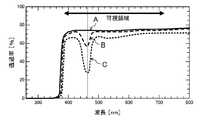
図1は、4H−SiC単結晶の光透過スペクトルを測定した結果を示したグラフである。測定は分光光度計を用いて行い、縦軸は透過率、横軸は波長を表す。図中の矢印A、B、Cで示したグラフは、それぞれ、n型不純物(窒素)の密度が1×1016cm−3、2×1018cm−3、5×1018cm−3のSiC単結晶の測定結果を表す。なお、半導体デバイスの製造用として商業的に利用できるSiC単結晶インゴットのn型不純物密度は、通常、2×1018cm−3〜8×1018cm−3の範囲にある。FIG. 1 is a graph showing the results of measuring the light transmission spectrum of a 4H-SiC single crystal. The measurement is performed using a spectrophotometer, and the vertical axis represents the transmittance and the horizontal axis represents the wavelength. The graphs indicated by arrows A, B, and C in the figure show the densities of n-type impurities (nitrogen) of 1 × 1016 cm-3 , 2 × 1018 cm-3 , and 5 × 1018 cm-3 , respectively. The measurement result of the SiC single crystal is shown. The n-type impurity density of a SiC single crystal ingot that can be commercially used for manufacturing semiconductor devices is usually in the range of2 × 10 18 cm-3 to 8 × 1018 cm-3.
図1に示すように、矢印Aで示したグラフでは、可視領域において光吸収はなかったが、矢印B、Cで示したグラフでは、約460nmの波長において光吸収(透過率減少)があった。また、n型不純物密度が高いほど、光吸収が大きかった。すなわち、n型不純物密度が2×1018cm−3、5×1018cm−3のSiC単結晶では、約460nmの波長で光吸収が起き、これが、琥珀色に着色する原因となる。As shown in FIG. 1, in the graph shown by arrow A, there was no light absorption in the visible region, but in the graphs shown by arrows B and C, there was light absorption (decreased transmittance) at a wavelength of about 460 nm. .. Further, the higher the density of n-type impurities, the greater the light absorption. That is, in a SiC single crystal having an n-type impurity density of 2 × 1018 cm-3 and 5 × 1018 cm-3 , light absorption occurs at a wavelength of about 460 nm, which causes amber coloring.
図2は、n型4H−SiC単結晶のバンド構造を示した図である。SiC単結晶は、第1伝導帯と、第2伝導帯があり、第1伝導帯には、n型不純物の準位(不図示)から励起された電子eが存在する。 FIG. 2 is a diagram showing a band structure of an n-type 4H-SiC single crystal. The SiC single crystal has a first conduction band and a second conduction band, and in the first conduction band, electrons e excited from the level (not shown) of n-type impurities are present.
SiC単結晶に入射した光は、第1伝導帯の底近傍に存在する電子を、第2伝導帯の底近傍に励起する。第1伝導帯の底のエネルギー準位Ec1と、第2伝導帯の底のエネルギー準位Ec2とのエネルギーギャップEg2は、約2.7eVである。2.7eVは、波長460nmの光エネルギーに相当する。そのため、n型不純物が導入されたSiC単結晶は、460nmの波長において光吸収が生じることになる。また、n型不純物の密度が高いほど、第1伝導帯の底近傍に存在する電子の数が多くなるため、光吸収も多くなる。The light incident on the SiC single crystal excites the electrons existing near the bottom of the first conduction band near the bottom of the second conduction band. The energy gap Eg2between the energy level E c1 at the bottom of the first conduction bandand the energy level E c2 at the bottom of the second conduction band is about 2.7 eV. 2.7 eV corresponds to light energy having a wavelength of 460 nm. Therefore, the SiC single crystal into which the n-type impurity is introduced will absorb light at a wavelength of 460 nm. Further, as the density of the n-type impurities increases, the number of electrons existing near the bottom of the first conduction band increases, so that the light absorption also increases.
本願発明者等は、SiC単結晶に電子線を照射すると、Si原子とC原子が弾き飛ばされて、空孔と格子間原子の格子欠陥が生成される現象に注目した。C原子の質量は、Si原子の質量よりも小さいため、原子を弾き飛ばすために必要な電子エネルギーは、Si原子よりC原子の方が小さい。そのため、SiC単結晶に電子線を照射した場合、炭素空孔と格子間炭素原子の生成が支配的になる。また、一旦生成された格子間炭素原子は、拡散定数が非常に大きく、電子線照射時の温度上昇や、電子線照射後の意図的な熱処理により、SiC結晶表面まで移動するため、SiC単結晶内には、ほとんど残らない。これにより、SiC単結晶に電子線を照射することによって、ほぼ炭素空孔だけを選択的に生成することができる。 The inventors of the present application have paid attention to a phenomenon in which when a SiC single crystal is irradiated with an electron beam, Si atoms and C atoms are blown off, and lattice defects of vacancies and interstitial atoms are generated. Since the mass of the C atom is smaller than the mass of the Si atom, the electron energy required to flick the atom is smaller in the C atom than in the Si atom. Therefore, when the SiC single crystal is irradiated with an electron beam, the formation of carbon vacancies and interstitial carbon atoms becomes dominant. In addition, the interstitial carbon atoms once generated have a very large diffusion constant and move to the surface of the SiC crystal due to the temperature rise during electron beam irradiation and the intentional heat treatment after electron beam irradiation, so that the SiC single crystal Almost nothing remains inside. As a result, by irradiating the SiC single crystal with an electron beam, almost only carbon vacancies can be selectively generated.
なお、本実施形態で言う「炭素空孔を含むSiC単結晶」は、格子点に1個の炭素空孔がある場合だけでなく、複数の炭素空孔が連なって存在するSiC単結晶も含む。また、炭素空孔と珪素空孔の対で構成される欠陥が存在するSiC単結晶も含む。 The "SiC single crystal containing carbon vacancies" referred to in the present embodiment includes not only the case where there is one carbon vacancies at the lattice points but also the SiC single crystal in which a plurality of carbon vacancies are continuously present. .. It also includes a SiC single crystal having a defect composed of a pair of carbon vacancies and silicon vacancies.
図3は、DLTS(Deep Level Transient Spectroscopy)法を用いて、電子線照射した4H−SiC単結晶の欠陥準位を測定した結果を示したDLTSスペクトルで、縦軸はDLTS信号強度、横軸は温度を表す。図中の矢印Aで示したスペクトルは、電子線照射する前の測定結果を示し、矢印Bで示したスペクトルは、電子線照射した後の測定結果を示し、矢印Cで示したスペクトルは、電子線照射後に熱処理したときの測定結果を示す。 FIG. 3 is a DLTS spectrum showing the results of measuring the defect level of an electron beam-irradiated 4H-SiC single crystal using the DLTS (Deep Level Transient Spectroscopy) method. Represents temperature. The spectrum shown by the arrow A in the figure shows the measurement result before the electron beam irradiation, the spectrum shown by the arrow B shows the measurement result after the electron beam irradiation, and the spectrum shown by the arrow C shows the electron. The measurement result when the heat treatment was performed after the radiation irradiation is shown.
ここで、電子線照射は、照射エネルギーを200keV、照射量を1×1016cm−2の条件で行った。また、熱処理は、950℃の窒素雰囲気中で、30分行った。Here, the electron beam irradiation was performed under the conditions of an irradiation energy of 200 keV and an irradiation amount of 1 × 1016 cm-2. The heat treatment was carried out in a nitrogen atmosphere at 950 ° C. for 30 minutes.
図3に示すように、電子線照射した後のSiC単結晶のDLTSスペクトルには、矢印P1、P2で示した2つのピークが現れている。また、電子線照射後に熱処理しても、2つのピークはほとんど変化しなかった。As shown in FIG. 3, the DLTS spectra of SiC single crystal after electron beam irradiation, the two peaks indicated by the arrows P1, P2 has appeared. Moreover, even if the heat treatment was performed after the electron beam irradiation, the two peaks hardly changed.
これら2つのピークは、電子線照射によりSiC単結晶内に生成された炭素空孔に起因した電子トラップと考えられ、2つのピークが現れる温度から、電子線照射した後のSiC単結晶のバンド構造は、図4に表すように、2つの炭素空孔による欠陥準位ED1(EC1―ED1=0.6eV)、ED2(EC1―ED2=1.5eV)が存在していると考えられる。These two peaks are considered to be electron traps caused by carbon vacancies generated in the SiC single crystal by electron beam irradiation, and from the temperature at which the two peaks appear, the band structure of the SiC single crystal after electron beam irradiation. , as represented in FIG. 4, two defect levelsE D1 (E C1 -E D1 = 0.6eV) with carbonvacancies, E D2 (E C1 -E D2 = 1.5eV) is present it is conceivable that.
従って、図4に示すように、この欠陥準位ED1、ED2に、n型不純物の準位から励起される電子を捕獲させれば、第1伝導帯に存在する電子をなくすことが可能となる。その結果、図2に示したような、第1伝導帯に存在する電子が、第2伝導帯に励起することによって生じる460nmの光吸収をなくすことが可能となる。Accordingly, as shown in FIG. 4, in the defect level ED1, ED2, if caused to capture electrons excited from the level of n-type impurity, it can be eliminated electrons in the first conduction band It becomes. As a result, as shown in FIG. 2, it is possible to eliminate the light absorption at 460 nm caused by the electrons existing in the first conduction band being excited to the second conduction band.
本発明は、かかる知見に基づきなされたもので、n型不純物を含むSiC単結晶に、電子線照射することによって、SiC単結晶内に炭素空孔を生成し、この炭素空孔の欠陥準位に、n型不純物の準位から励起される電子を捕獲させることによって、460nmの光吸収をなくし、これにより、n型不純物を含むSiC単結晶の無色化を図るものである。 The present invention has been made based on such findings. By irradiating a SiC single crystal containing n-type impurities with an electron beam, carbon vacancies are generated in the SiC single crystal, and the defect level of the carbon vacancies is generated. By capturing the electrons excited from the level of the n-type impurity, the light absorption at 460 nm is eliminated, thereby making the SiC single crystal containing the n-type impurity colorless.
図5は、n型不純物を含むSiC単結晶に電子線照射した後の光透過スペクトルを測定した結果を示したグラフである。図中の矢印Bで示したグラフは、電子線照射する前のSiC単結晶(n型不純物密度が5×1018cm−3)の測定結果を示し、矢印Cで示したグラフは、電子線照射(照射エネルギー:1MeV、照射量:4.5×1018cm−2)した後の測定結果を示す。なお、図中の矢印Aで示したグラフは、n型不純物が低密度(1×1016cm−3)のSiC単結晶の測定結果を示す。FIG. 5 is a graph showing the results of measuring the light transmission spectrum of a SiC single crystal containing an n-type impurity after irradiation with an electron beam. The graph indicated by the arrow B in the figure shows the measurement result of the SiC single crystal (n-type impurity density is 5 × 1018 cm-3 ) before the electron beam irradiation, and the graph indicated by the arrow C is the electron beam. The measurement result after irradiation (irradiation energy: 1 MeV, irradiation amount: 4.5 × 1018 cm-2) is shown. The graph indicated by the arrow A in the figure shows the measurement results of a SiC single crystal having a low density of n-type impurities (1 × 1016 cm-3).
図5に示すように、矢印Bで示したグラフでは460nmの光吸収が見られたが、矢印Cで示したグラフでは460nmの光吸収は見られなかった。すなわち、一定量のn型不純物を含むSiC単結晶は、電子線照射することによって、460nmの光吸収をなくして無色化を図ることができる。 As shown in FIG. 5, the graph indicated by arrow B showed light absorption at 460 nm, but the graph indicated by arrow C did not show light absorption at 460 nm. That is, a SiC single crystal containing a certain amount of n-type impurities can be made colorless by irradiating with an electron beam to eliminate light absorption at 460 nm.
図2に示したように、n型不純物を含むSiC単結晶において、第1伝導帯に存在する電子密度は、n型不純物密度とほぼ等しい。従って、図4に示したように、炭素空孔の欠陥準位に電子を捕獲することによって、460nmの光吸収をなくして無色化を図るためには、炭素空孔の密度を、少なくともn型不純物の密度よりも多くすることが好ましい。 As shown in FIG. 2, in the SiC single crystal containing n-type impurities, the electron density existing in the first conduction band is substantially equal to the n-type impurity density. Therefore, as shown in FIG. 4, in order to eliminate light absorption at 460 nm and achieve colorlessness by capturing electrons at the defect level of carbon vacancies, the density of carbon vacancies should be at least n-type. It is preferably higher than the density of impurities.
電子線照射によって生成される炭素空孔の生成量は、電子線照射の照射エネルギー及び照射量が高いほど多い。従って、460nmの光吸収をなくして無色化を図るためには、電子線照射の照射エネルギー及び照射量を、炭素空孔の密度が、少なくともn型不純物の密度よりも多くなるように設定すればよい。 The amount of carbon vacancies generated by electron beam irradiation increases as the irradiation energy and irradiation amount of electron beam irradiation increase. Therefore, in order to eliminate light absorption at 460 nm and achieve colorlessness, the irradiation energy and irradiation amount of electron beam irradiation should be set so that the density of carbon pores is at least higher than the density of n-type impurities. Good.
SiC単結晶内に生成される炭素空孔の存在、及び炭素空孔の密度は、炭素空孔密度が低い場合は、DLTS法を用いて測定することができる。また、炭素空孔密度が高い場合は、電子スピン共鳴(ESR:Electron Spin Resonance)法を用いて測定することができる。 The presence of carbon vacancies generated in the SiC single crystal and the density of carbon vacancies can be measured by using the DLTS method when the carbon vacancies density is low. When the carbon pore density is high, it can be measured by using an electron spin resonance (ESR) method.
図6は、ESR法を用いて、電子線照射したSiC単結晶中に生成された欠陥準位を測定した結果の例を示したグラフで、縦軸はESR信号を表し、横軸は磁束密度を表す。 FIG. 6 is a graph showing an example of the result of measuring the defect level generated in the SiC single crystal irradiated with an electron beam by using the ESR method. The vertical axis represents the ESR signal, and the horizontal axis represents the magnetic flux density. Represents.
図6に示すように、電子線照射したSiC単結晶のESRスペクトルには、矢印Q1、Q2で示した2つのピークが観察され、これらのピークは、電子線照射によりSiC単結晶内に生成された炭素空孔の欠陥準位に起因したものと考えられる。また、2つのピークにおけるESR信号の高さから、生成された炭素空孔密度は、約8×1017cm−3と推定される。As shown in FIG. 6, the ESR spectrum of the electron beam irradiated SiC single crystal, is observed two peaks indicated by arrows Q1, Q2, these peaks are in the SiC single crystal by electron beam irradiation It is considered that this was caused by the defect level of the generated carbon vacancies. Also, from the height of the ESR signals at the two peaks, the carbon pore density generated is estimated to beabout 8 × 10 17 cm-3.
本実施形態によれば、n型不純物が導入された有色のSiC単結晶に電子線照射することによって、SiC単結晶内に一定の密度の炭素空孔を生成し、この炭素空孔の欠陥準位に、n型不純物の準位から励起される電子を捕獲させることによって、n型不純物を含むSiC単結晶に固有の460nmの光吸収をなくすことができ、これにより、無色化されたSiC単結晶を得ることができる。 According to the present embodiment, by irradiating a colored SiC single crystal into which an n-type impurity is introduced with an electron beam, carbon vacancies having a constant density are generated in the SiC single crystal, and the defects of the carbon vacancies are quasi. By capturing the electrons excited from the level of the n-type impurity at the position, the light absorption of 460 nm peculiar to the SiC single crystal containing the n-type impurity can be eliminated, thereby making the SiC single crystal colorless. Crystals can be obtained.
このようにして得られた無色のSiC単結晶は、合成宝石用結晶体として提供することができ、適当な大きさにカットすることによって、無色透明な合成宝石を作製することができる。また、この方法を用いることにより、半導体デバイスの製造用として商業的に利用できるSiC単結晶インゴットを用いて、輝きを有する無色透明な合成宝石を、比較的安い価格で提供することができる。 The colorless SiC single crystal thus obtained can be provided as a crystal for synthetic gemstones, and by cutting into an appropriate size, a colorless and transparent synthetic gemstone can be produced. Further, by using this method, it is possible to provide a colorless and transparent synthetic gemstone having brilliance at a relatively low price by using a SiC single crystal ingot that can be commercially used for manufacturing a semiconductor device.
ところで、SiC単結晶インゴットは、バルクな単結晶体であるため、SiC単結晶インゴットをカットして、無色透明な合成宝石を得るには、バルクな結晶体全体に、一定の密度の炭素空孔を生成する必要がある。 By the way, since the SiC single crystal ingot is a bulk single crystal, in order to cut the SiC single crystal ingot and obtain a colorless and transparent synthetic gemstone, carbon pores having a constant density are formed in the entire bulk crystal. Need to be generated.
図7は、SiC単結晶に電子線照射して、SiC単結晶内に生成された炭素空孔密度の深さ方向の分布を測定して結果を示したグラフである。縦軸は、生成された炭素空孔密度を表し、横軸は、表面からの深さを表す。また、測定は、DLTS法を用いて、SiC単結晶を、深さ方向に研磨を繰り返しながら行った。 FIG. 7 is a graph showing the results of measuring the distribution of the carbon pore density generated in the SiC single crystal in the depth direction by irradiating the SiC single crystal with an electron beam. The vertical axis represents the density of carbon pores produced, and the horizontal axis represents the depth from the surface. Further, the measurement was carried out by using the DLTS method while repeatedly polishing the SiC single crystal in the depth direction.
図中の矢印A、B、C、D、Eで示したグラフは、それぞれ、電子線照射の照射エネルギーを、250eV、500eV、750eV、1.0MeV、3.0MeVとしたときの結果を示す。また、電子線照射の照射量は、全て1×1016cm−3とした。The graphs indicated by arrows A, B, C, D, and E in the figure show the results when the irradiation energies of electron beam irradiation are 250 eV, 500 eV, 750 eV, 1.0 MeV, and 3.0 MeV, respectively. The irradiation amount of electron beam irradiation was set to 1 × 1016 cm-3 .
図7に示すように、照射エネルギーが高いほど、SiC単結晶の奥深くまで炭素空孔を生成させることができる。また、照射エネルギーが高いほど、炭素空孔の生成量も多くなる。なお、図7の測定では、照射量を1×1016cm−3としたが、照射量を多くすることによって、炭素空孔の生成量も多くすることができる。As shown in FIG. 7, the higher the irradiation energy, the deeper the carbon vacancies can be generated in the SiC single crystal. In addition, the higher the irradiation energy, the larger the amount of carbon vacancies generated. In the measurement of FIG. 7, the irradiation amount was set to 1 × 1016 cm-3 , but by increasing the irradiation amount, the amount of carbon vacancies generated can also be increased.
このように、n型不純物を含むSiC単結晶に電子線照射することによって、SiC単結晶の無色透明化を図るためには、SiC単結晶全体に亘って、460nmの光吸収をなくすために必要な炭素空孔密度になるように、電子線照射の照射エネルギー及び照射量を設定すればよい。 In this way, in order to make the SiC single crystal colorless and transparent by irradiating the SiC single crystal containing n-type impurities with an electron beam, it is necessary to eliminate light absorption at 460 nm over the entire SiC single crystal. The irradiation energy and irradiation amount of electron beam irradiation may be set so that the carbon pore density is high.
図8は、電子線照射によりSiC単結晶内に生成された炭素空孔の生成率と、電子線照射の照射エネルギーとの関係を示したグラフである。ここで、炭素空孔の生成率は、以下の式(1)により求めた。 FIG. 8 is a graph showing the relationship between the generation rate of carbon vacancies generated in a SiC single crystal by electron beam irradiation and the irradiation energy of electron beam irradiation. Here, the formation rate of carbon vacancies was calculated by the following formula (1).

ここで、(式1)の分子の炭素空孔密度は、照射したSiC結晶表面近傍の値である。表面から奥深い領域では、図7で示したように、炭素空孔密度は減少する。 Here, the carbon pore density of the molecule of (Equation 1) is a value near the surface of the irradiated SiC crystal. In the region deep from the surface, the carbon pore density decreases, as shown in FIG.
図8に示すように、電子線照射の照射エネルギーが高いほど、炭素空孔の生成率は高くなる。ここで、生成される炭素空孔密度は、電子線照射の照射量にほぼ比例するので、460nmの光吸収をなくすために必要な炭素空孔密度が分かれば、図8のグラフから、電子線照射の照射エネルギーに対して必要な照射量を求めることができる。 As shown in FIG. 8, the higher the irradiation energy of the electron beam irradiation, the higher the formation rate of carbon vacancies. Here, the carbon pore density generated is substantially proportional to the irradiation amount of electron beam irradiation. Therefore, if the carbon pore density required to eliminate light absorption at 460 nm is known, the electron beam can be seen from the graph of FIG. The required irradiation amount can be obtained for the irradiation energy of the irradiation.
例えば、密度が5×1018cm−3の炭素空孔を、照射エネルギーが1MeVの電子線照射で生成するのに必要な照射量は、3.9×1018cm−2(5×1018cm−3/1.28cm−1)となる。For example, the amount of irradiation required to generate carbon vacancies with a density of 5 × 1018 cm-3 by electron beam irradiation with an irradiation energy of 1 MeV is 3.9 × 1018 cm-2 (5 × 10¹⁸). It becomes cm-3 / 1.28cm -1).
図9は、SiC単結晶における波長460nmの光吸収係数と、SiC単結晶に導入されたn型不純物の密度との関係を示したグラフである。測定は分光光度計を用いて行い、縦軸は光吸収係数を表し、横軸はn型不純物密度を表す。 FIG. 9 is a graph showing the relationship between the light absorption coefficient of a SiC single crystal having a wavelength of 460 nm and the density of n-type impurities introduced into the SiC single crystal. The measurement is performed using a spectrophotometer, the vertical axis represents the light absorption coefficient, and the horizontal axis represents the n-type impurity density.
図9に示すように、波長460nmの光吸収係数は、n型不純物密度が7×1016cm−3以上では、n型不純物密度にほぼ比例している。また、n型不純物密度が7×1016cm−3以下のSiC単結晶では、光吸収係数が2cm−1以下あり、厚さ5mmのSiC単結晶でも、光が透過し透明となる。一方、n型不純物密度が1×1017cm−3以上のSiC単結晶では、光吸収係数が5cm−1以上となり、厚さ2mm以上のSiC単結晶では、無色透明にならない。As shown in FIG. 9, the light absorption coefficient at a wavelength of 460 nm is substantially proportional to then-type impurity density when the n-type impurity density is 7 × 10 16 cm-3 or higher. Further, a SiC single crystal having an n-type impurity density of 7 × 1016 cm-3 or less has a light absorption coefficient of 2 cm-1 or less, and even a SiC single crystal having a thickness of 5 mm transmits light and becomes transparent. On the other hand, a SiC single crystal having an n-type impurity density of 1 × 1017 cm-3 or more has a light absorption coefficient of 5 cm-1 or more, and a SiC single crystal having a thickness of 2 mm or more is not colorless and transparent.
本発明は、このような有色不透明なSiC単結晶に対して、無色透明化に有効な手段を提供する。すなわち、図9に示すように、Aで示す範囲(n型不純物密度が1×1017cm−2以上)のn型不純物を含むSiC単結晶に、電子線照射することによって、Bで示す範囲のように、波長460nmの光吸収係数が2cm−1以下の無色透明なSiC単結晶に変えることができる。なお、n型不純物密度が5×1017cm−2以上の場合、波長460nmの光吸収係数が10cm−1以上になるため、本発明による効果がより発揮される。The present invention provides an effective means for making such a colored opaque SiC single crystal colorless and transparent. That is, as shown in FIG. 9, the range shown in B is obtained by irradiating the SiC single crystal containing the n-type impurities in the range shown in A (n-type impurity density is 1 × 1017 cm-2 or more) with an electron beam. As described above, it is possible to change to a colorless and transparent SiC single crystal having a light absorption coefficient of 2 cm-1 or less at a wavelength of 460 nm. When the density of n-type impurities is 5 × 1017 cm-2 or more, the light absorption coefficient at a wavelength of 460 nm is 10 cm-1 or more, so that the effect of the present invention is more exhibited.
ここで、電子線照射の照射エネルギー及び照射量は、炭素空孔の密度が、n型不純物の密度よりも多くなるように設定すればよい。また、SiC単結晶の厚さに応じて、電子線照射の照射エネルギーは適宜決めればよい。 Here, the irradiation energy and irradiation amount of electron beam irradiation may be set so that the density of carbon vacancies is higher than the density of n-type impurities. Further, the irradiation energy of electron beam irradiation may be appropriately determined according to the thickness of the SiC single crystal.
半導体デバイスの製造用として商業的に利用できるSiC単結晶インゴットは、通常、n型不純物密度が1×1018cm−3以上である。本発明は、特に、このような高密度のn型不純物を含むSiC単結晶インゴットに対して、無色透明化を図るのに有効であり、本発明を適用することによって、無色透明な合成宝石用結晶体を比較的安い価格で提供することが可能になる。Commercially available SiC single crystal ingots for the manufacture of semiconductor devices typically have an n-type impurity density of 1 × 1018 cm-3 or higher. The present invention is particularly effective for making a SiC single crystal ingot containing such a high-density n-type impurity colorless and transparent, and by applying the present invention, it is used for colorless and transparent synthetic jewels. It becomes possible to provide crystals at a relatively low price.
半導体デバイスの製造用のSiC単結晶インゴットは、n型不純物を添加せずに作製することもできる。しかしながら、このような無添加のSiC単結晶インゴットでも、通常、n型不純物となる窒素が、1×1017cm−3〜5×1017cm−3の密度で、残留不純物として存在するため、薄い琥珀色が付いている。このような低密度のSiC単結晶インゴットは、僅かな量の炭素空孔を生成することによって、簡単に無色透明化することができる。そのため、電子線照射の照射量を少なくすることができ、無色透明な合成宝石用結晶体をより安価に提供することが可能になる。The SiC single crystal ingot for manufacturing a semiconductor device can also be manufactured without adding n-type impurities. However, even in such an additive-free SiC single crystal ingot, nitrogen, which is an n-type impurity, usually exists as a residual impurity at a density of1 × 10 17 cm-3 to 5 × 1017 cm-3. It has a light amber color. Such a low-density SiC single crystal ingot can be easily made colorless and transparent by forming a small amount of carbon vacancies. Therefore, the irradiation amount of electron beam irradiation can be reduced, and a colorless and transparent crystal for synthetic gemstone can be provided at a lower cost.
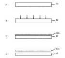
図10(A)〜(D)は、本実施形態における合成宝石用結晶体の製造方法を示した図である。 10 (A) to 10 (D) are views showing a method for producing a crystal for synthetic gemstones in the present embodiment.
まず、図10(A)に表すように、n型不純物を含むSiC単結晶体10を用意する。SiC単結晶体10は、例えば、半導体デバイスの製造用として商業的に利用できるSiC単結晶インゴットを用いることができる。 First, as shown in FIG. 10A, a SiC
次に、図10(B)に表すように、SiC単結晶体10に電子線照射することにより、SiC単結晶体10内に、炭素空孔を生成する。ここで、電子線照射の照射エネルギー及び照射量は、炭素空孔の密度が、n型不純物の密度よりも多くなるように設定される。これにより、図10(C)に表すように、SiC単結晶体10の表面下に、炭素空孔が生成された欠陥領域10Aが形成される。なお、SiC単結晶体10の厚みが薄い場合は、SiC単結晶体10全体に欠陥領域10Aが形成される。 Next, as shown in FIG. 10B, by irradiating the SiC
次に、図10(D)に表すように、SiC単結晶体10の欠陥領域10Aを切り離す。欠陥領域10Aの切り離しは、例えば、欠陥領域10AとSiC単結晶体10の界面を、細いダイヤモンドワイヤソーで切断することによって行うことができる。切り離された欠陥領域10Aは無色透明化された合成宝石用結晶体として提供することができ、これを適当な大きさにカットすることによって、無色透明な合成宝石を作製することができる。なお、残りのSiC結晶体10は原材料として再利用できる。例えば、このSiC結晶体10に電子線照射を施すことによって、表面領域を無色透明化し、この領域を合成宝石用結晶体として提供することができる。また、別の目的(例えば、半導体デバイスの製造用の基板)に再利用することもできる。 Next, as shown in FIG. 10 (D), the
なお、SiC単結晶体10に電子線照射したとき、炭素空孔が生成される以外に、格子間炭素原子が僅かに残る場合がある。この場合、格子間炭素原子によって、僅かな光吸収が生じ、透明度が低下することもある。そのため、透明度の低下を防止する目的で、炭素空孔を生成する工程の後、SiC単結晶体10を500℃〜1400℃の温度で熱処理してもよい。 When the SiC
以上、本発明を好適な実施形態により説明してきたが、こうした記述は限定事項ではなく、もちろん、種々の改変が可能である。例えば、上記実施形態では、4H−SiC単結晶について説明したが、6H−SiC単結晶についても、電子線照射により、炭素空孔の生成が可能で、4H−SiC単結晶の場合と炭素空孔の生成量は同一であるため、4H−SiC単結晶と同様の効果を得ることができる。 Although the present invention has been described above in terms of preferred embodiments, such a description is not a limitation, and of course, various modifications can be made. For example, in the above embodiment, the 4H-SiC single crystal has been described, but the 6H-SiC single crystal can also generate carbon vacancies by electron beam irradiation, and the case of the 4H-SiC single crystal and the carbon vacancies can be generated. Since the amount of the above is the same, the same effect as that of the 4H-SiC single crystal can be obtained.
また、電子線照射により、SiC単結晶に生成された炭素空孔は、必ずしも均一に分布していなくてもよく、460nmの光吸収をなくすために必要な密度の炭素空孔が存在していればよい。 Further, the carbon pores generated in the SiC single crystal by electron beam irradiation do not necessarily have to be uniformly distributed, and carbon pores having a density required to eliminate light absorption at 460 nm should be present. Just do it.
また、電子線照射により生成された炭素空孔は、必ずしもSiC単結晶全体に亘って存在していなくてもよく、SiC単結晶の表面から、一定の深さの領域に存在していればよい。この場合、SiC単結晶の炭素空孔が生成された領域だけを切り出すことによって、無色透明な合成宝石用結晶体を得ることができる。 Further, the carbon vacancies generated by electron beam irradiation do not necessarily have to exist over the entire SiC single crystal, and may be present in a region of a certain depth from the surface of the SiC single crystal. .. In this case, a colorless and transparent crystal for synthetic gemstone can be obtained by cutting out only the region where the carbon vacancies of the SiC single crystal are generated.
また、合成宝石用結晶体に用いるSiC単結晶は、必ずしも、半導体デバイスの製造用として商業的に利用できるSiC単結晶インゴットに限らず、他の目的で製造されたSiC単結晶でもよく、勿論、合成宝石用に製造されたSiC単結晶であってもよい。 Further, the SiC single crystal used for the crystal for synthetic jewelry is not necessarily limited to the SiC single crystal ingot that can be commercially used for manufacturing semiconductor devices, and may be a SiC single crystal manufactured for other purposes, and of course. It may be a SiC single crystal manufactured for synthetic jewels.
10 SiC単結晶体
10A 欠陥領域
10 SiC
Claims (5)
Translated fromJapanese前記SiC単結晶体に電子線照射することにより、前記SiC単結晶体内に、炭素空孔を生成する工程と、
を含み、
前記電子線照射の照射エネルギー及び照射量は、前記炭素空孔の密度が、前記n型不純物の密度よりも多くなるように設定される、合成宝石用結晶体の製造方法。A step of preparing a SiC single crystal containing n-type impurities, and
A step of forming carbon vacancies in the SiC single crystal by irradiating the SiC single crystal with an electron beam, and
Including
A method for producing a crystal for synthetic gemstones, wherein the irradiation energy and irradiation amount of the electron beam irradiation are set so that the density of the carbon pores is larger than the density of the n-type impurities.
The synthesis according to any one of claims 1 to 3, wherein the n-type impurity ispresent as a residual impurity in the SiC single crystal at a density of 1 × 10 17 cm-3 to 5 × 1017 cm-3. A method for producing a crystal for gemstones.
Priority Applications (3)
| Application Number | Priority Date | Filing Date | Title |
|---|---|---|---|
| JP2021017259AJP6903362B1 (en) | 2021-02-05 | 2021-02-05 | Method for manufacturing crystals for synthetic gemstones |
| US17/535,787US11725301B2 (en) | 2021-02-05 | 2021-11-26 | Method for manufacturing crystal for synthetic gem |
| CN202111465301.8ACN114164498B (en) | 2021-02-05 | 2021-12-03 | Method for producing crystal for synthetic gem |
Applications Claiming Priority (1)
| Application Number | Priority Date | Filing Date | Title |
|---|---|---|---|
| JP2021017259AJP6903362B1 (en) | 2021-02-05 | 2021-02-05 | Method for manufacturing crystals for synthetic gemstones |
Publications (2)
| Publication Number | Publication Date |
|---|---|
| JP6903362B1true JP6903362B1 (en) | 2021-07-14 |
| JP2022120393A JP2022120393A (en) | 2022-08-18 |
Family
ID=76753246
Family Applications (1)
| Application Number | Title | Priority Date | Filing Date |
|---|---|---|---|
| JP2021017259AActiveJP6903362B1 (en) | 2021-02-05 | 2021-02-05 | Method for manufacturing crystals for synthetic gemstones |
Country Status (3)
| Country | Link |
|---|---|
| US (1) | US11725301B2 (en) |
| JP (1) | JP6903362B1 (en) |
| CN (1) | CN114164498B (en) |
Families Citing this family (1)
| Publication number | Priority date | Publication date | Assignee | Title |
|---|---|---|---|---|
| JP2024017630A (en) | 2022-07-28 | 2024-02-08 | Hoya株式会社 | Image correction method for electronic endoscope system |
Family Cites Families (6)
| Publication number | Priority date | Publication date | Assignee | Title |
|---|---|---|---|---|
| US5762896A (en) | 1995-08-31 | 1998-06-09 | C3, Inc. | Silicon carbide gemstones |
| US5718760A (en)* | 1996-02-05 | 1998-02-17 | Cree Research, Inc. | Growth of colorless silicon carbide crystals |
| US5882786A (en) | 1996-11-15 | 1999-03-16 | C3, Inc. | Gemstones formed of silicon carbide with diamond coating |
| US7601441B2 (en)* | 2002-06-24 | 2009-10-13 | Cree, Inc. | One hundred millimeter high purity semi-insulating single crystal silicon carbide wafer |
| JP5155536B2 (en)* | 2006-07-28 | 2013-03-06 | 一般財団法人電力中央研究所 | Method for improving the quality of SiC crystal and method for manufacturing SiC semiconductor device |
| CN100467679C (en)* | 2007-04-20 | 2009-03-11 | 山东大学 | Colored moissanite single crystal and its preparation method and preparation of artificial gemstones |
- 2021
- 2021-02-05JPJP2021017259Apatent/JP6903362B1/enactiveActive
- 2021-11-26USUS17/535,787patent/US11725301B2/enactiveActive
- 2021-12-03CNCN202111465301.8Apatent/CN114164498B/enactiveActive
Also Published As
| Publication number | Publication date |
|---|---|
| US11725301B2 (en) | 2023-08-15 |
| CN114164498A (en) | 2022-03-11 |
| US20220251729A1 (en) | 2022-08-11 |
| JP2022120393A (en) | 2022-08-18 |
| CN114164498B (en) | 2022-05-27 |
Similar Documents
| Publication | Publication Date | Title |
|---|---|---|
| JP5874932B2 (en) | Method for processing diamond material and product obtained | |
| US9255009B2 (en) | Diamond material | |
| JP6980893B2 (en) | Semiconductor wafers made from single crystal silicon and their manufacturing process | |
| JP6903362B1 (en) | Method for manufacturing crystals for synthetic gemstones | |
| JP2019536730A (en) | Single crystal synthetic diamond material by chemical vapor deposition | |
| JP2015531337A (en) | Single crystal chemical vapor deposition synthetic diamond material with uniform color | |
| Boukhvalov et al. | Structural, electronic, and optical properties of 6H-SiC layers synthesized by implantation of carbon ions into silicon | |
| Khomich et al. | Effect of neutron irradiation on the hydrogen state in CVD diamond films | |
| RU2237113C1 (en) | Method of manufacturing diamonds in fantasy red color | |
| Grigoriev et al. | The radiation hard BGO crystals for astrophysics applications | |
| Shlimak et al. | On the doping of isotopically controlled germanium by nuclear transmutation with a high concentration of shallow donor impurities | |
| Vodakov et al. | Progress in the growth and research of crystals for wide-gap semiconducting materials | |
| Jayavel et al. | Raman scattering studies on low-energy nitrogen-implanted semi-insulating GaAs | |
| WO2022210935A1 (en) | Single crystal diamond and method for producing same | |
| Kuriyama et al. | Effect on the excess P element in P-ion-implanted semi-insulating Fe-doped InP | |
| Maekawa et al. | Hole trap annealing in neutron-transmutation-doped silicon with different initial resistivities | |
| JPH06326044A (en) | Semiconductor si substrate and manufacture of the same | |
| HK1170274B (en) | Method for treating diamond material and product obtained | |
| KR20080096940A (en) | Manufacturing method of yellow diamond |
Legal Events
| Date | Code | Title | Description |
|---|---|---|---|
| A621 | Written request for application examination | Free format text:JAPANESE INTERMEDIATE CODE: A621 Effective date:20210205 | |
| A871 | Explanation of circumstances concerning accelerated examination | Free format text:JAPANESE INTERMEDIATE CODE: A871 Effective date:20210205 | |
| RD01 | Notification of change of attorney | Free format text:JAPANESE INTERMEDIATE CODE: A7426 Effective date:20210304 | |
| A975 | Report on accelerated examination | Free format text:JAPANESE INTERMEDIATE CODE: A971005 Effective date:20210416 | |
| A521 | Request for written amendment filed | Free format text:JAPANESE INTERMEDIATE CODE: A821 Effective date:20210304 | |
| A131 | Notification of reasons for refusal | Free format text:JAPANESE INTERMEDIATE CODE: A131 Effective date:20210427 | |
| A521 | Request for written amendment filed | Free format text:JAPANESE INTERMEDIATE CODE: A523 Effective date:20210430 | |
| TRDD | Decision of grant or rejection written | ||
| A01 | Written decision to grant a patent or to grant a registration (utility model) | Free format text:JAPANESE INTERMEDIATE CODE: A01 Effective date:20210608 | |
| A61 | First payment of annual fees (during grant procedure) | Free format text:JAPANESE INTERMEDIATE CODE: A61 Effective date:20210616 | |
| R150 | Certificate of patent or registration of utility model | Ref document number:6903362 Country of ref document:JP Free format text:JAPANESE INTERMEDIATE CODE: R150 | |
| R250 | Receipt of annual fees | Free format text:JAPANESE INTERMEDIATE CODE: R250 |