JP6900231B2 - Touch detection device and method - Google Patents
Touch detection device and methodDownload PDFInfo
- Publication number
- JP6900231B2 JP6900231B2JP2017085167AJP2017085167AJP6900231B2JP 6900231 B2JP6900231 B2JP 6900231B2JP 2017085167 AJP2017085167 AJP 2017085167AJP 2017085167 AJP2017085167 AJP 2017085167AJP 6900231 B2JP6900231 B2JP 6900231B2
- Authority
- JP
- Japan
- Prior art keywords
- coil
- differential amplifier
- output
- operational amplifier
- touch detection
- Prior art date
- Legal status (The legal status is an assumption and is not a legal conclusion. Google has not performed a legal analysis and makes no representation as to the accuracy of the status listed.)
- Active
Links
Images


Classifications
- G—PHYSICS
- G06—COMPUTING OR CALCULATING; COUNTING
- G06F—ELECTRIC DIGITAL DATA PROCESSING
- G06F3/00—Input arrangements for transferring data to be processed into a form capable of being handled by the computer; Output arrangements for transferring data from processing unit to output unit, e.g. interface arrangements
- G06F3/01—Input arrangements or combined input and output arrangements for interaction between user and computer
- G06F3/03—Arrangements for converting the position or the displacement of a member into a coded form
- G06F3/041—Digitisers, e.g. for touch screens or touch pads, characterised by the transducing means
- G06F3/0416—Control or interface arrangements specially adapted for digitisers
- G06F3/04166—Details of scanning methods, e.g. sampling time, grouping of sub areas or time sharing with display driving
- G—PHYSICS
- G06—COMPUTING OR CALCULATING; COUNTING
- G06F—ELECTRIC DIGITAL DATA PROCESSING
- G06F3/00—Input arrangements for transferring data to be processed into a form capable of being handled by the computer; Output arrangements for transferring data from processing unit to output unit, e.g. interface arrangements
- G06F3/01—Input arrangements or combined input and output arrangements for interaction between user and computer
- G06F3/03—Arrangements for converting the position or the displacement of a member into a coded form
- G06F3/041—Digitisers, e.g. for touch screens or touch pads, characterised by the transducing means
- G06F3/0412—Digitisers structurally integrated in a display
- G—PHYSICS
- G06—COMPUTING OR CALCULATING; COUNTING
- G06F—ELECTRIC DIGITAL DATA PROCESSING
- G06F3/00—Input arrangements for transferring data to be processed into a form capable of being handled by the computer; Output arrangements for transferring data from processing unit to output unit, e.g. interface arrangements
- G06F3/01—Input arrangements or combined input and output arrangements for interaction between user and computer
- G06F3/03—Arrangements for converting the position or the displacement of a member into a coded form
- G06F3/041—Digitisers, e.g. for touch screens or touch pads, characterised by the transducing means
- G06F3/046—Digitisers, e.g. for touch screens or touch pads, characterised by the transducing means by electromagnetic means
- G—PHYSICS
- G06—COMPUTING OR CALCULATING; COUNTING
- G06F—ELECTRIC DIGITAL DATA PROCESSING
- G06F2203/00—Indexing scheme relating to G06F3/00 - G06F3/048
- G06F2203/041—Indexing scheme relating to G06F3/041 - G06F3/045
- G06F2203/04103—Manufacturing, i.e. details related to manufacturing processes specially suited for touch sensitive devices
- G—PHYSICS
- G06—COMPUTING OR CALCULATING; COUNTING
- G06F—ELECTRIC DIGITAL DATA PROCESSING
- G06F2203/00—Indexing scheme relating to G06F3/00 - G06F3/048
- G06F2203/041—Indexing scheme relating to G06F3/041 - G06F3/045
- G06F2203/04108—Touchless 2D- digitiser, i.e. digitiser detecting the X/Y position of the input means, finger or stylus, also when it does not touch, but is proximate to the digitiser's interaction surface without distance measurement in the Z direction
Landscapes
- Engineering & Computer Science (AREA)
- General Engineering & Computer Science (AREA)
- Theoretical Computer Science (AREA)
- Physics & Mathematics (AREA)
- Human Computer Interaction (AREA)
- General Physics & Mathematics (AREA)
- Electromagnetism (AREA)
- Position Input By Displaying (AREA)
Description
Translated fromJapanese本発明の実施形態はタッチ検出装置及び方法に関する。 Embodiments of the present invention relate to touch detection devices and methods.
スマートフォン、タブレットパーソナルコンピュータ及びノート型パーソナルコンピュータ等の携帯端子末が普及している。携帯端子末は液晶又は有機EL素子などを用いた平面型表示装置を備える。表示装置は2次元配列された画素を備え、画素は共通電極と画素電極を備え、共通電極と画素電極との間に液晶又は有機EL素子が配置される。ドライバが画素に画素信号を書き込むと、共通電極及び画素電極との間の液晶又は有機EL素子が制御され、画像が表示される。 Mobile terminal terminals for smartphones, tablet personal computers, notebook personal computers, and the like are widespread. The end of the mobile terminal is provided with a flat display device using a liquid crystal or an organic EL element. The display device includes pixels arranged in two dimensions, the pixels include a common electrode and a pixel electrode, and a liquid crystal or organic EL element is arranged between the common electrode and the pixel electrode. When the driver writes a pixel signal to the pixel, the liquid crystal or organic EL element between the common electrode and the pixel electrode is controlled and an image is displayed.
一方、画面に指やタッチペン(スタイラスペンとも称する)等の入力物体が近接又は接触していることを検出するタッチパネルが広く使用されている。画面に入力物体を近接又は接触させる動作をタッチ動作又はタッチと称し、入力物体の位置検出をタッチ検出と称する。ペンを用いると、指より小さい領域の指定や手書き文字の入力がより容易である。ペンによるタッチを検出する方式は種々あり、その一つの方式として電磁誘導方式がある。電磁誘導方式では、ペンはコイルと容量を含み、タッチパネルは送信コイルと受信コイルを含み、タッチパネルの送信コイルが磁界を発生し、ペンの容量に磁界エネルギーが蓄えられ、タッチパネルの受信コイルがその磁界を検出する。 On the other hand, a touch panel that detects that an input object such as a finger or a touch pen (also referred to as a stylus pen) is in close proximity or in contact with the screen is widely used. The operation of bringing the input object close to or in contact with the screen is referred to as touch operation or touch, and the position detection of the input object is referred to as touch detection. Using a pen makes it easier to specify areas smaller than the finger and to enter handwritten characters. There are various methods for detecting a touch with a pen, and one of them is an electromagnetic induction method. In the electromagnetic induction method, the pen contains a coil and a capacitance, the touch panel includes a transmitting coil and a receiving coil, the transmitting coil of the touch panel generates a magnetic field, the magnetic field energy is stored in the capacitance of the pen, and the receiving coil of the touch panel is the magnetic field. Is detected.
このような電磁誘導方式のタッチ検出機能を備える表示装置では、表示装置の寄生容量や寄生抵抗の影響によりノイズが発生し、正確な検出が困難である。
本発明の目的は、正確な検出が可能である電磁誘導方式のタッチ検出機能を備えるタッチ検出装置及び方法を提供することである。In a display device having such an electromagnetic induction type touch detection function, noise is generated due to the influence of the parasitic capacitance and the parasitic resistance of the display device, and accurate detection is difficult.
An object of the present invention is to provide a touch detection device and method having an electromagnetic induction type touch detection function capable of accurate detection.
実施形態によれば、タッチ検出装置はタッチパネルと、差動増幅器と、比較器と、補償回路を具備する。タッチパネルは送信コイルと受信コイルを具備し、表示機能とタッチ検出機能を備える。受信コイルの両端が差動増幅器の2つの入力端子に接続される。比較器は、送信コイルに供給された駆動信号と、差動増幅器の出力信号との位相さを検出する。補償回路は、差動増幅器の位相遅延を補償する。駆動信号は補償回路を介して比較器に入力される。According to the embodiment, the touch detection device includes a touch panel,a differential amplifier,a comparator, and a compensation circuit . The touch panel includes a transmission coil and a reception coil, and has a display function and a touch detection function. Both ends of the receiving coil are connected to the two input terminals of the differential amplifier.The comparator detects the phase of the drive signal supplied to the transmission coil and the output signal of the differential amplifier. The compensation circuit compensates for the phase delay of the differential amplifier. The drive signal is input to the comparator via a compensation circuit.
以下、実施の形態について図面を参照して説明する。なお、開示はあくまで一例にすぎず、以下の実施形態に記載した内容により発明が限定されるものではない。当業者が容易に想到し得る変形は当然に開示の範囲に含まれる。説明をより明確にするため、図面において、各部分のサイズ、形状等を実物通りではなく変更して模式的に表す場合もあるし、構造物を区別するために付したハッチングを省略する場合もある。複数の図面において、対応する要素には同じ参照数字を付して詳細な説明を省略する場合もある。 Hereinafter, embodiments will be described with reference to the drawings. The disclosure is merely an example, and the invention is not limited by the contents described in the following embodiments. Modifications that can be easily conceived by those skilled in the art are naturally included in the scope of disclosure. In order to clarify the explanation, in the drawings, the size, shape, etc. of each part may be changed and represented schematically, or the hatching attached to distinguish the structure may be omitted. is there. In a plurality of drawings, the corresponding elements may be given the same reference numbers and detailed description may be omitted.
タッチ検出機能付き表示装置は、表示装置とタッチパネルを別々に製造し、表示装置の画面にタッチパネルを貼り付けるオンセルタイプ(外付けタイプとも称する)と、表示装置とタッチパネルが一体となっているインセルタイプ(内蔵タイプとも称する)を含む。インセルタイプの表示装置は、タッチ検出機能を有する部品の一部又は全部が表示機能を有する部品の一部又は全部と兼用される装置や、タッチ検出機能を有する部品と表示機能を有する部品とが互いに兼用されない装置を含む。インセルタイプの表示装置では、例えばカラーフィルタと偏光板の間に検出電極が形成され、TFT基板上に形成される共通電極が駆動電極としても使用される。インセルタイプの表示装置は、外付けタッチパネルが無いので、全体が薄型・軽量化されるとともに、表示の視認性も向上する。実施形態はインセルタイプの表示装置を説明するが、本発明はオンセルタイプの表示装置にも適用可能である。 The display device with touch detection function is an on-cell type (also called an external type) in which the display device and the touch panel are manufactured separately and the touch panel is attached to the screen of the display device, and the in-cell in which the display device and the touch panel are integrated. Includes types (also referred to as built-in types). The in-cell type display device includes a device in which a part or all of a part having a touch detection function is also used as a part or all of a part having a display function, and a part having a touch detection function and a part having a display function. Includes devices that are not shared with each other. In an in-cell type display device, for example, a detection electrode is formed between a color filter and a polarizing plate, and a common electrode formed on a TFT substrate is also used as a drive electrode. Since the in-cell type display device does not have an external touch panel, the entire display is made thinner and lighter, and the visibility of the display is also improved. Although the embodiment describes an in-cell type display device, the present invention is also applicable to an on-cell type display device.
表示装置は液晶表示装置、有機EL表示装置、プラズマディスプレイ表示装置等を利用することができるが、一例として、液晶表示装置を用いた実施形態を説明するが、本発明は有機EL表示装置、プラズマディスプレイ表示装置等にも適用可能である。液晶表示装置の表示モードは表示機能層である液晶層の液晶分子の配向を変化させるための電界の印加方向により大きく2つに分類される。第1は表示装置の厚さ方向(あるいは面外方向)に電界が印加される所謂縦電界モードである。縦電界モードは例えばTN(Twisted Nematic)モードや、VA(Vertical Alignment)モード等を含む。第2は表示装置の平面方向(あるいは面内方向)に電界が印加される所謂横電界モードである。横電界モードは例えばIPS(In-Plane Switching)モードや、IPSモードの一つであるFFS(Fringe Field Switching)モード等を含む。以下で説明する技術は縦電界モードおよび横電界モードのいずれにも適用できるが、実施形態としては横電界モードの表示装置を説明する。 As the display device, a liquid crystal display device, an organic EL display device, a plasma display display device, or the like can be used. As an example, an embodiment using the liquid crystal display device will be described, but the present invention describes the organic EL display device, plasma. It can also be applied to display devices and the like. The display mode of the liquid crystal display device is roughly classified into two according to the application direction of the electric field for changing the orientation of the liquid crystal molecules in the liquid crystal layer which is the display function layer. The first is a so-called vertical electric field mode in which an electric field is applied in the thickness direction (or out-of-plane direction) of the display device. The vertical electric field mode includes, for example, a TN (Twisted Nematic) mode, a VA (Vertical Alignment) mode, and the like. The second is a so-called lateral electric field mode in which an electric field is applied in the plane direction (or in-plane direction) of the display device. The transverse electric field mode includes, for example, an IPS (In-Plane Switching) mode, an FFS (Fringe Field Switching) mode which is one of the IPS modes, and the like. The technique described below can be applied to both the longitudinal electric field mode and the transverse electric field mode, but as an embodiment, a display device of the transverse electric field mode will be described.
(第1実施形態)
[概略構造]
図1は実施形態によるタッチ検出機能付きの表示装置の一例の全体的な概略構成例を示す斜視図である。表示装置はタッチパネルPNLと表示駆動回路とタッチ検出回路等を備える。タッチパネルPNLはガラス、樹脂等の透明な第1基板SUB1と、第1基板SUB1に対向配置されたガラス、樹脂等の透明な第2基板SUB2と、第1基板SUB1及び第2基板SUB2との間に形成された液晶層(図示せず)を備える。第1基板SUB1にはTFT(Thin Film Transistor)の画素がマトリクス状に形成されるので、第1基板SUB1は画素基板又はアレイ基板とも称する。第2基板SUB2は対向基板とも称する。タッチパネルPNLは第2基板SUB2側から観察される。このため、第2基板SUB2は上側基板、第1基板SUB1は下側基板と称することもある。第1基板SUB1は複数の導体パターンを有する。複数の導体パターンは、複数の走査線、複数の信号線、複数の駆動電極、複数の画素電極を含む。駆動電極はITO(Indium tin oxide)又はIZO(Indium Zinc Oxide)等の透明な導電材料により構成されても良い。第2基板SUB2は遮光膜であるブラックマトリクス、カラーフィルタ等を備える。(First Embodiment)
[Outline structure]
FIG. 1 is a perspective view showing an overall schematic configuration example of an example of a display device with a touch detection function according to an embodiment. The display device includes a touch panel PNL, a display drive circuit, a touch detection circuit, and the like. The touch panel PNL is between a transparent first substrate SUB1 such as glass and resin, a transparent second substrate SUB2 such as glass and resin arranged to face the first substrate SUB1, and a first substrate SUB1 and a second substrate SUB2. It is provided with a liquid crystal layer (not shown) formed in. Since the pixels of the TFT (Thin Film Transistor) are formed in a matrix on the first substrate SUB1, the first substrate SUB1 is also referred to as a pixel substrate or an array substrate. The second substrate SUB2 is also referred to as a facing substrate. The touch panel PNL is observed from the second substrate SUB2 side. Therefore, the second substrate SUB2 may be referred to as an upper substrate, and the first substrate SUB1 may be referred to as a lower substrate. The first substrate SUB1 has a plurality of conductor patterns. The plurality of conductor patterns include a plurality of scanning lines, a plurality of signal lines, a plurality of driving electrodes, and a plurality of pixel electrodes. The drive electrode may be made of a transparent conductive material such as ITO (Indium tin oxide) or IZO (Indium Zinc Oxide). The second substrate SUB2 includes a black matrix which is a light-shielding film, a color filter, and the like.
タッチパネルPNLは矩形の平板形状であり、短辺が沿う方向をX方向、長辺が沿う方向をY方向とする。第1基板SUB1と第2基板SUB2は短辺のサイズは同じであるが、長辺のサイズが異なり、第1基板SUB1の方が第2基板SUB2より長い。長辺方向において第1基板SUB1の一端子と第2基板SUB2の一端子が揃っているので、第1基板SUB1の他端子は第2基板SUB2の他端子より突出している。長辺方向において第2基板SUB2より突出している第1基板SUB1の部分には、タッチパネルPNLを画像表示のために駆動する表示駆動回路を構成するパネルドライバIC1が搭載される。パネルドライバIC1はCOG(Chip on Glass)チップからなる。パネルドライバはドライバチップ又は表示コントローラとも称する。第1基板SUB1の中央部の表示領域又はアクティブエリアDAには、TFTの画素アレイが形成される。 The touch panel PNL has a rectangular flat plate shape, and the direction along which the short side is along is the X direction, and the direction along which the long side is along is the Y direction. The first substrate SUB1 and the second substrate SUB2 have the same short side size, but the long side size is different, and the first substrate SUB1 is longer than the second substrate SUB2. Since one terminal of the first substrate SUB1 and one terminal of the second substrate SUB2 are aligned in the long side direction, the other terminals of the first substrate SUB1 protrude from the other terminals of the second substrate SUB2. A panel driver IC1 constituting a display drive circuit for driving a touch panel PNL for image display is mounted on a portion of the first substrate SUB1 protruding from the second substrate SUB2 in the long side direction. The panel driver IC1 is composed of a COG (Chip on Glass) chip. The panel driver is also called a driver chip or a display controller. A pixel array of TFTs is formed in the display area or active area DA in the central portion of the first substrate SUB1.
第1基板SUB1の裏側(つまり、タッチパネルPNLの背面側)には、タッチパネルPNLを照明する照明装置としてのバックライトユニットBLが配置される。バックライトユニットBLとしては、種々の形態のバックライトユニットが利用可能であり、光源としては、発光ダイオード(LED)を利用したもの及び冷陰極管(CCFL)を利用したもの等がある。照明装置は、タッチパネルPNLの背面側に配置される導光板と、そのサイドに配置されるLED又は冷陰極管により構成されてもよいし、タッチパネルPNLの背面側に発光素子を平面的に配列した点状光源により構成されてもよい。照明装置は、バックライトに限らず、タッチパネルPNLの表示面側に配置されるフロントライトを使用してもよい。さらに、反射型の表示装置の場合、又はタッチパネルPNLが有機ELを用いる場合、照明装置を備えない構成でもよい。 A backlight unit BL as a lighting device for illuminating the touch panel PNL is arranged on the back side of the first substrate SUB1 (that is, the back side of the touch panel PNL). As the backlight unit BL, various types of backlight units can be used, and as the light source, there are those using a light emitting diode (LED) and those using a cold cathode tube (CCFL). The lighting device may be composed of a light guide plate arranged on the back side of the touch panel PNL and an LED or a cold cathode tube arranged on the side thereof, or light emitting elements are arranged in a plane on the back side of the touch panel PNL. It may be composed of a point light source. The lighting device is not limited to the backlight, and a front light arranged on the display surface side of the touch panel PNL may be used. Further, in the case of a reflective display device or when the touch panel PNL uses an organic EL, a configuration without a lighting device may be provided.
表示装置はホスト装置HOSTに接続され得る。タッチパネルPNLとホスト装置HOSTは3つのフレキシブル配線基板FPC1、FPC2、FPC3を介して接続される。ホスト装置HOSTはフレキシブル配線基板FPC1を介して第1基板SUB1に接続される。ホスト装置HOSTはフレキシブル配線基板FPC2を介して第2基板SUB2に接続される。ホスト装置HOSTはフレキシブル配線基板FPC3を介してバックライトユニットBLに接続される。 The display device may be connected to the host device HOST. The touch panel PNL and the host device HOST are connected via three flexible wiring boards FPC1, FPC2, and FPC3. The host device HOST is connected to the first board SUB1 via the flexible wiring board FPC1. The host device HOST is connected to the second substrate SUB2 via the flexible wiring board FPC2. The host device HOST is connected to the backlight unit BL via the flexible wiring board FPC3.
タッチ検出を制御するタッチパネルコントローラIC2がフレキシブル配線基板FPC2上に形成される。タッチパネルコントローラIC2はCOF(Chip on Film)チップからなる。タッチパネルコントローラIC2はタッチ検出チップ又はタッチコントローラとも称する。タッチパネルコントローラIC2は、フレキシブル配線基板FPC2上に形成されるCOFチップではなく、第1基板SUB1上に形成されるCOGチップでもよい。同様に、パネルドライバIC1は、第1基板SUB1上に形成されるCOGチップではなく、フレキシブル配線基板FPC2上に形成されるCOFチップでもよい。 A touch panel controller IC2 that controls touch detection is formed on the flexible wiring board FPC2. The touch panel controller IC2 is composed of a COF (Chip on Film) chip. The touch panel controller IC2 is also referred to as a touch detection chip or a touch controller. The touch panel controller IC2 may be a COG chip formed on the first substrate SUB1 instead of the COF chip formed on the flexible wiring board FPC2. Similarly, the panel driver IC1 may be a COF chip formed on the flexible wiring board FPC2 instead of the COG chip formed on the first substrate SUB1.
パネルドライバIC1とタッチパネルコントローラIC2とは、相互に動作タイミングが連携しており、タイミングパルスなどで互いに電気的に接続される。パネルドライバIC1とタッチパネルコントローラIC2は、別々のICチップではなく、同一のICチップとして構成されてもよい。この場合、単一のICチップは第1基板SUB1上に形成してもよいし、フレキシブルFPC2上に形成してもよい。 The operation timings of the panel driver IC1 and the touch panel controller IC2 are linked to each other, and they are electrically connected to each other by a timing pulse or the like. The panel driver IC1 and the touch panel controller IC2 may be configured as the same IC chip instead of separate IC chips. In this case, the single IC chip may be formed on the first substrate SUB1 or on the flexible FPC2.
図示していないが、表示装置は2次電池及び電源回路等を備える。また、後述するように、表示装置はタッチ検出のためのコイルを備える。
[画素アレイ]
図2は画素アレイの一例を示すブロック回路図である。第1基板SUB1の表示領域DAは行方向(X方向)に延びる複数の走査線GLと駆動電極TLと、列方向(Y方向)に延びる複数の信号線SLを備える。表示領域DAに画素アレイが形成される。画素は液晶素子LCとTFT(Thin Film Transistor)からなるスイッチング素子SWを有する。各行の画素のスイッチング素子SWのゲート端子はX方向に延びるゲート線GLに共通に接続される。ゲート線GLの両端子は表示領域DAの左右の額縁領域まで引き出され、額縁領域に配置されたゲート回路24に接続される。ゲート回路24は表示期間に画素を行毎に選択的にオンさせる。ゲート回路24は表示領域DAの左右の額縁領域に配置する必要は無く、図2に示すように、片側の額縁領域だけにゲート回路24を配置してもよい。Although not shown, the display device includes a secondary battery, a power supply circuit, and the like. Further, as will be described later, the display device includes a coil for touch detection.
[Pixel array]
FIG. 2 is a block circuit diagram showing an example of a pixel array. The display area DA of the first substrate SUB1 includes a plurality of scanning lines GL extending in the row direction (X direction), a drive electrode TL, and a plurality of signal lines SL extending in the column direction (Y direction). A pixel array is formed in the display area DA. The pixel has a switching element SW composed of a liquid crystal element LC and a TFT (Thin Film Transistor). The gate terminal of the switching element SW of the pixel of each row is commonly connected to the gate line GL extending in the X direction. Both terminals of the gate line GL are drawn out to the left and right frame areas of the display area DA, and are connected to the
各列の画素のスイッチング素子SWのソース端子又はドレイン端子はY方向に延びる信号線(ソース線とも称する)SLに共通に接続される。信号線SLの一端子は上又は下の額縁領域まで引き出され、額縁領域に配置されたパネルドライバIC1内のソース増幅器22に接続される。ソース増幅器22は表示期間に選択的にオンされている画素行の各列の画素に表示のための映像信号を供給する。映像信号は赤、緑、青の3色の色成分の映像信号からなり、ホスト装置HOSTからパネルドライバIC1に供給される映像信号は、赤、緑、青の3色の色成分の映像信号が多重化された信号である。そのため、図示しないが、パネルドライバIC1は、多重化信号を赤、緑、青の3色の色成分の映像信号に分離するマルチプレクサを含み、各画素には赤、緑、青の3色の色成分の映像信号のいずれかが供給される。 The source terminal or drain terminal of the switching element SW of each row of pixels is commonly connected to a signal line (also referred to as a source line) SL extending in the Y direction. One terminal of the signal line SL is drawn out to the upper or lower frame area and connected to the
各画素のスイッチング素子SWのドレイン端子又はソース端子は液晶素子LCの一端子に接続される。各行の画素の液晶素子LCの他端子はX方向に延びる駆動電極TLに共通に接続される。駆動電極TLの両端子は表示領域DAの左右の額縁領域まで引き出され、額縁領域に配置されたTX駆動回路26に接続される。TX駆動回路26はタッチ検出期間に駆動電極TLにタッチ駆動信号TXを供給する。TX駆動回路26は表示期間に駆動電極TLに一定の直流電圧を供給する。タッチパネルでは、タッチ検出期間と表示期間が交互に繰り返される。TX駆動回路26は表示領域DAの左右の額縁領域に配置する必要はなく、図2に示すように、片側の額縁領域だけにTX駆動回路26を配置してもよい。 The drain terminal or source terminal of the switching element SW of each pixel is connected to one terminal of the liquid crystal element LC. The other terminals of the liquid crystal element LC of the pixels in each row are commonly connected to the drive electrode TL extending in the X direction. Both terminals of the drive electrode TL are drawn out to the left and right frame areas of the display area DA, and are connected to the
パネルドライバIC1はゲート回路24、TX駆動回路26を制御するとともに、タッチパネルコントローラIC2と連携する。タッチパネルコントローラIC2は、タッチ検出信号を処理し、表示面に対するペンの接触位置の座標データを得る。座標データはホスト装置HOSTに入力される。パネルドライバIC1はホスト装置HOSTと相互通信を行い、データの要求・受信などを行う。ホスト装置HOSTは、パネルドライバIC1に対して映像データ、コマンド、同期信号などを供給することができる。パネルドライバIC1は座標データに基づいて所定のコマンドを入力してもよいし、座標データの軌跡を手書き文字として表示してもよい。 The panel driver IC1 controls the
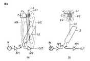
[電磁誘導方式のタッチ検出原理]
図3に示すように、液晶表示装置1は金属カバー内に収納され、導光板とセンサ板と磁性シートを備える。センサ板は種々の位置に配置可能であるが、図3では、例えば液晶表示装置1と金属カバーとの間に実装される。センサ板には複数のコイルが設けられる。センサ板に設けられている複数のコイルのうちの1個のコイルをセンサ板内コイルL2(単にコイルL2とも称する)として模式的に示す。[Electromagnetic induction touch detection principle]
As shown in FIG. 3, the liquid crystal display device 1 is housed in a metal cover and includes a light guide plate, a sensor plate, and a magnetic sheet. The sensor plate can be arranged at various positions, but in FIG. 3, it is mounted, for example, between the liquid crystal display device 1 and the metal cover. A plurality of coils are provided on the sensor plate. One coil of the plurality of coils provided on the sensor plate is schematically shown as a coil L2 in the sensor plate (also simply referred to as a coil L2).
ペンはコイルと容量素子(図示省略)とを内蔵する。コイルはペン内コイルL1(単にコイルL1とも称する)として模式的に示される。コイルL1とコイルL2との間は磁界によって結合(磁界結合)される。
液晶表示装置1はTFTガラス基板(第1基板SUB1に対応)とカラーフィルタとCFガラス基板(第2基板SUB2に対応)とを備える。TFTガラス基板上にTFT(図示せず)が形成され、TFTガラス基板上とTFT(図示せず)からなる構造体をTFT基板とも称する。CFガラス基板とカラーフィルタからなり構造体をカラーフィルタ基板とも称する。TFT基板とカラーフィルタ基板との間には図示しない液晶層が挟持される。導光板は、液晶表示装置1とセンサ板との間に挟まれるように固定部で固定される。The pen has a built-in coil and a capacitive element (not shown). The coil is schematically shown as an in-pen coil L1 (also simply referred to as coil L1). The coil L1 and the coil L2 are coupled (magnetic field coupling) by a magnetic field.
The liquid crystal display device 1 includes a TFT glass substrate (corresponding to the first substrate SUB1), a color filter, and a CF glass substrate (corresponding to the second substrate SUB2). A structure in which a TFT (not shown) is formed on a TFT glass substrate and the structure is composed of the TFT glass substrate and the TFT (not shown) is also referred to as a TFT substrate. A structure composed of a CF glass substrate and a color filter is also referred to as a color filter substrate. A liquid crystal layer (not shown) is sandwiched between the TFT substrate and the color filter substrate. The light guide plate is fixed by a fixing portion so as to be sandwiched between the liquid crystal display device 1 and the sensor plate.
ペンが表示装置1に近接している又は接触している場合、コイルL1がコイルL2に近接又は接触し、コイルL1とコイルL2との間の磁界結合が発生し、ペンの近接又は接触が検出される。
図4を参照して検出の原理を説明する。図4(a)はコイルL2が磁界を発生している状態を示し、図4(b)はコイルL1が磁界を発生している状態を示す。When the pen is close to or in contact with the display device 1, the coil L1 is close to or in contact with the coil L2, a magnetic field coupling occurs between the coil L1 and the coil L2, and the closeness or contact of the pen is detected. Will be done.
The principle of detection will be described with reference to FIG. FIG. 4A shows a state in which the coil L2 is generating a magnetic field, and FIG. 4B shows a state in which the coil L1 is generating a magnetic field.
ペンにおいて、コイルL1とペン内容量素子(単に容量素子とも称する)Cとは並列的に接続され、共振回路を構成する。コイルL2の巻線数は何回でも構わないが、図4では1回巻線のコイルL2が示される。コイルL2は1対の端子を有する。タッチ検出の際、コイルL2は一定期間に送信アンプAP1の出力端子に接続され、一定期間経過後に接続が切り替えられ、次の一定期間に受信アンプAP2の入力端子に接続される。説明の便宜上、図4は、コイルL2の一端子PTが送信アンプAP1又は、受信アンプAP2に接続され、他端子が接地されている様子を示すが、後述するように、実施形態では、タッチ検出の際、コイルL2の両端子が差動方式の増幅器の2つの入力端子に接続される。 In the pen, the coil L1 and the pen internal capacitance element (also simply referred to as a capacitive element) C are connected in parallel to form a resonance circuit. The number of windings of the coil L2 may be any number of times, but FIG. 4 shows the coil L2 having one winding. The coil L2 has a pair of terminals. At the time of touch detection, the coil L2 is connected to the output terminal of the transmitting amplifier AP1 for a certain period of time, the connection is switched after a certain period of time has elapsed, and the coil L2 is connected to the input terminal of the receiving amplifier AP2 for a certain period of time. For convenience of explanation, FIG. 4 shows a state in which one terminal PT of the coil L2 is connected to the transmission amplifier AP1 or the reception amplifier AP2 and the other terminals are grounded. However, as will be described later, in the embodiment, touch detection is performed. At this time, both terminals of the coil L2 are connected to the two input terminals of the differential amplifier.
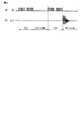
図5(a)、(b)はタッチ検出を示す波形図である。図5(a)、(b)において、横軸は時間を示し、図5(a)は送信アンプAP1の出力波形を示しており、図5(b)は受信アンプAP2の出力波形を示す。図5は1つのタッチ検出期間内の動作を示す。 5 (a) and 5 (b) are waveform diagrams showing touch detection. In FIGS. 5A and 5B, the horizontal axis represents time, FIG. 5A shows the output waveform of the transmitting amplifier AP1, and FIG. 5B shows the output waveform of the receiving amplifier AP2. FIG. 5 shows the operation within one touch detection period.
最初の一定期間である磁界発生期間TGTに、周期的に変化する送信信号INが送信アンプAP1に入力され、コイルL2は送信アンプAP1の出力端子に接続される。このため、送信アンプAP1は磁界発生期間TGTに、図5(a)に示すように、送信信号INの増幅信号である駆動信号をコイルL2に供給する。これにより、コイルL2が磁界を発生する。図4(a)では、このときの磁力線がφGとして示されている。 During the magnetic field generation period TGT, which is the first fixed period, a periodically changing transmission signal IN is input to the transmission amplifier AP1, and the coil L2 is connected to the output terminal of the transmission amplifier AP1. Therefore, the transmission amplifier AP1 supplies the drive signal, which is the amplification signal of the transmission signal IN, to the coil L2 during the magnetic field generation period TGT, as shown in FIG. 5A. As a result, the coil L2 generates a magnetic field. In FIG. 4A, the magnetic force line at this time is shown as φG.
磁力線φGはコイルL2の巻線を中心として発生するため、コイルL2の内側の磁界が強くなる。ペンが表示装置1に近接又は接触し、図4(a)に示すように、コイルL1の中心軸L0がコイルL2のループ内側に存在すると、コイルL1にコイルL2の磁力線φGが到達する。すなわち、コイルL1がコイルL2において発生している磁界内に配置され、コイルL1とコイルL2とが磁界結合される。コイルL2は送信信号INの増幅信号である駆動信号に従って周期的に変化する磁界φGを発生する。そのため、コイルL2とコイルL1間の相互誘導の作用により、コイルL1に誘起電圧が生じる。容量素子CはコイルL1に生じた誘起電圧によって充電される。 Since the magnetic force line φG is generated around the winding of the coil L2, the magnetic field inside the coil L2 becomes strong. When the pen approaches or comes into contact with the display device 1 and the central axis L0 of the coil L1 exists inside the loop of the coil L2 as shown in FIG. 4A, the magnetic force line φG of the coil L2 reaches the coil L1. That is, the coil L1 is arranged in the magnetic field generated in the coil L2, and the coil L1 and the coil L2 are magnetically coupled. The coil L2 generates a magnetic field φG that changes periodically according to a drive signal that is an amplified signal of the transmission signal IN. Therefore, an induced voltage is generated in the coil L1 due to the mutual induction action between the coil L2 and the coil L1. The capacitive element C is charged by the induced voltage generated in the coil L1.
磁界発生期間TGTが経過すると、コイルL2は次の一定期間である磁界検出期間又は電流検出期間TDTに受信アンプAP2の入力端子に接続される。磁界検出期間TDTに、送信信号INは送信アンプAP1に入力されない。先の磁界発生期間TGTにおいて容量素子Cが充電されていれば、磁界検出期間TDTにおいてコイルL1は容量素子Cに充電された電荷によって磁界を発生する。図4(b)では、容量素子Cに充電された電荷によって発生したコイルL1の磁力線がφDとして示されている。 When the magnetic field generation period TGT elapses, the coil L2 is connected to the input terminal of the receiving amplifier AP2 during the next fixed period, the magnetic field detection period or the current detection period TDT. During the magnetic field detection period TDT, the transmission signal IN is not input to the transmission amplifier AP1. If the capacitive element C is charged in the previous magnetic field generation period TGT, the coil L1 generates a magnetic field by the electric charge charged in the capacitive element C in the magnetic field detection period TDT. In FIG. 4B, the magnetic force line of the coil L1 generated by the electric charge charged in the capacitive element C is shown as φD.
ペンが表示装置1に近接又は接触していれば、磁界発生期間TGTに容量素子Cは充電され、磁界検出期間TDTにコイルL1の磁力線φDがコイルL2に到達する。コイルL1と容量素子Cとにより共振回路が構成されているため、コイルL1の発する磁界は共振回路の時定数に従って変化する。コイルL1が発生する磁界が変化することにより、コイルL2に誘起電圧が生じる。この誘起電圧によってコイルL2の一方の端子PTにおける信号が変化する。この信号の変化が磁界検出期間TDTに検出信号として受信アンプAP2に入力され、増幅され、誘起電圧に応じて変化するセンサ信号OUTが受信アンプAP2から出力される。 If the pen is close to or in contact with the display device 1, the capacitance element C is charged during the magnetic field generation period TGT, and the magnetic force line φD of the coil L1 reaches the coil L2 during the magnetic field detection period TDT. Since the resonance circuit is composed of the coil L1 and the capacitive element C, the magnetic field generated by the coil L1 changes according to the time constant of the resonance circuit. An induced voltage is generated in the coil L2 by changing the magnetic field generated by the coil L1. This induced voltage changes the signal at one terminal PT of the coil L2. The change in this signal is input to the receiving amplifier AP2 as a detection signal during the magnetic field detection period TDT, is amplified, and the sensor signal OUT that changes according to the induced voltage is output from the receiving amplifier AP2.
一方、コイルL1がコイルL2に近接又は接触していなければ、磁界発生期間TGTに容量素子Cは充電されない、または充電されたとしても充電電荷量は少ない。その結果、磁界検出期間TDTにコイルL1が発する磁界の磁力線φDはコイルL2に到達せず、磁界検出期間TDTにコイルL2が接続される受信アンプAP2からは一定のセンサ信号OUTが出力される。 On the other hand, if the coil L1 is not in close proximity to or in contact with the coil L2, the capacitive element C is not charged during the magnetic field generation period TGT, or even if it is charged, the charge amount is small. As a result, the magnetic force line φD of the magnetic field generated by the coil L1 during the magnetic field detection period TDT does not reach the coil L2, and a constant sensor signal OUT is output from the receiving amplifier AP2 to which the coil L2 is connected to the magnetic field detection period TDT.
図5(a)、(b)はペンが表示装置1に近接又は接触していない時(左側)と、近接又は接触している時(右側)の両方の状態を示す。ペンが表示装置1に近接又は接触していない時は、図5(b)の左側に示すように、磁界検出期間TDTに受信アンプAP2からは一定のセンサ信号OUTが出力される。ペンが表示装置1に近接又は接触している時は、図5(b)の右側に示すように、磁界検出期間TDTに受信アンプAP2からは変動するセンサ信号OUTが出力される。センサ信号OUTが変動している場合を「ペン有り」と判定し、センサ信号OUTが一定である場合を「ペン無し」と判定することにより、ペンによるタッチを検出することができる。図5では「ペン有り」と「ペン無し」が判定されるが、コイルL1とコイルL2との間の距離に従ってセンサ信号OUTの振幅が変化するため、ペンと表示装置(センサ板)との間の距離又はペンの筆圧を判定することも可能である。なお、磁界発生期間TGTから磁界検出期間TDTへの切り替え時にコイルL2の接続を送信アンプAP1の出力端子から受信アンプAP2の入力端子へ切り替える場合、コイルL2を送信アンプAP1の出力端子から切り離した後、コイルL2に蓄積されたエネルギーが放電するまでの所定時間だけコイルL2の端子PTをフローティング状態にし、その後に受信アンプAP2の入力端子に接続するようにしてもよい。 FIGS. 5A and 5B show states both when the pen is in close proximity or not in contact with the display device 1 (left side) and when the pen is in close proximity or in contact with the display device 1 (right side). When the pen is not in close proximity to or in contact with the display device 1, a constant sensor signal OUT is output from the receiving amplifier AP2 during the magnetic field detection period TDT, as shown on the left side of FIG. 5 (b). When the pen is in close proximity to or in contact with the display device 1, the receiving amplifier AP2 outputs a fluctuating sensor signal OUT during the magnetic field detection period TDT, as shown on the right side of FIG. 5B. A touch by the pen can be detected by determining that the sensor signal OUT is fluctuating as "with a pen" and determining that the sensor signal OUT is constant as "without a pen". In FIG. 5, "with pen" and "without pen" are determined, but since the amplitude of the sensor signal OUT changes according to the distance between the coil L1 and the coil L2, the space between the pen and the display device (sensor plate) is changed. It is also possible to determine the distance of the pen or the pen pressure. When switching the connection of the coil L2 from the output terminal of the transmission amplifier AP1 to the input terminal of the reception amplifier AP2 when switching from the magnetic field generation period TGT to the magnetic field detection period TDT, after disconnecting the coil L2 from the output terminal of the transmission amplifier AP1. The terminal PT of the coil L2 may be floated for a predetermined time until the energy stored in the coil L2 is discharged, and then connected to the input terminal of the receiving amplifier AP2.
[回路構成]
タッチ検出原理の説明では、磁界発生と磁界検出を同じコイル(センサ板内コイルL2)で行ったが、実施形態においては、磁界発生に用いるコイルと磁界検出に用いるコイルとが異なってもよい。例えば、磁界発生期間TGTに駆動電極TLにより送信コイルを形成して送信コイルにより磁界を発生してもよいし、磁界検出期間TDTに信号線SLにより受信コイルを形成して受信コイルにより磁界を検出してもよい。この場合も、タッチ検出原理は、図3〜図5で説明した原理と同じである。すなわち、ペン内コイルL1は、磁界発生期間TGTに、駆動電極により形成された送信コイルにより発生された磁界に基づいて誘起電圧を発生し、容量素子C(図4)を充電する。信号線により形成された受信コイルは、磁界検出期間TDTに、ペン内コイルL1により発生された磁界に基づいて誘起電圧を発生し、信号線における電圧の変化をタッチ検出の結果を表すセンス信号(検出信号とも称する)として出力する。[Circuit configuration]
In the explanation of the touch detection principle, the magnetic field generation and the magnetic field detection are performed by the same coil (coil L2 in the sensor plate), but in the embodiment, the coil used for the magnetic field generation and the coil used for the magnetic field detection may be different. For example, a transmission coil may be formed by the drive electrode TL in the magnetic field generation period TGT to generate a magnetic field by the transmission coil, or a reception coil may be formed by a signal line SL in the magnetic field detection period TDT and the magnetic field is detected by the reception coil. You may. In this case as well, the touch detection principle is the same as the principle described with reference to FIGS. 3 to 5. That is, the coil L1 in the pen generates an induced voltage based on the magnetic field generated by the transmission coil formed by the drive electrode during the magnetic field generation period TGT, and charges the capacitive element C (FIG. 4). The receiving coil formed by the signal line generates an induced voltage based on the magnetic field generated by the coil L1 in the pen during the magnetic field detection period TDT, and the change in the voltage in the signal line is a sense signal representing the result of touch detection ( It is also called a detection signal).
図6はインセル型のタッチパネルPNLの一例を示すブロック回路図である。2本あるいはそれ以上の偶数本の駆動電極TLをループ状に接続することにより送信コイルTX_COILが形成され、2本あるいはそれ以上の偶数本の信号線SLをループ状に接続することにより受信コイルRX_COILが形成される。駆動電極TL、信号線SLの両端子にそれぞれスイッチが接続される。スイッチを選択的にオンすることにより、2本あるいはそれ以上の偶数本の駆動電極TL又は信号線SLを互いに接続し、1本のループ状のコイルを形成することができる。駆動電極TLから構成される送信コイルTX_COILはX方向に細長い形状であり、信号線SLから構成される受信コイルRX_COILはY方向に細長い形状である。複数の送信コイルTX_COILはY方向に配列され、複数の受信コイルRX_COILはX方向に配列される。 FIG. 6 is a block circuit diagram showing an example of an in-cell type touch panel PNL. The transmission coil TX_COIL is formed by connecting two or more even-numbered drive electrodes TL in a loop, and the reception coil RX_COIL is formed by connecting two or more even-numbered signal lines SL in a loop. Is formed. Switches are connected to both the drive electrode TL and the signal line SL terminals, respectively. By selectively turning on the switch, two or more even-numbered drive electrodes TL or signal line SL can be connected to each other to form one loop-shaped coil. The transmitting coil TX_COIL composed of the drive electrode TL has an elongated shape in the X direction, and the receiving coil RX_COIL composed of the signal line SL has an elongated shape in the Y direction. The plurality of transmitting coils TX_COIL are arranged in the Y direction, and the plurality of receiving coils RX_COIL are arranged in the X direction.
送信コイルTX_COILの両端子は第1基板SUB1上のTX駆動回路26に接続される。TX駆動回路26は複数の送信コイルTX_COILにタッチ駆動信号TX(図4の送信信号INに相当)を順次供給し、複数の送信コイルTX_COILをスキャン駆動する。これにより、複数の送信コイルTX_COILが順次磁界を発生する。図5の1つの磁界発生期間TGTに多数の駆動信号TXが1つの送信コイルRX_COILに供給されてもよい。1つの磁界発生期間TGTに1つの送信コイルTX_COILから磁界を発生し、次の磁界検出期間に全ての受信コイルRX_COILの誘起電圧を調べる。送信コイルTX_COILと誘起電圧を検出した受信コイルRX_COILとの交点がタッチ位置であると判断でき、交点の座標がタッチ座標とされる。なお、送信コイルTX_COILを構成する駆動電極TLの数を変えて、送信コイルTX_COILのサイズ/数を変えることもできる。タッチ位置の検出精度は送信コイルのサイズ/数によるので、大きなサイズの少数の送信コイルTX_COILを用いて概略位置を検出してから、小さなサイズの多数の送信コイルTX_COILを用いて詳細位置を検出するようにしてもよい。 Both terminals of the transmission coil TX_COIL are connected to the
各受信コイルRX_COILの両端子は検出回路621〜62m(62と総称することもある)にそれぞれ接続される。検出回路621〜62mはタッチパネルコントローラIC2内に形成される。タッチパネルコントローラIC2内には高周波パルスであるタッチ駆動信号TXを発生するパルス発生器68も形成される。検出回路621〜62mの出力はタッチパネルコントローラIC2内に形成されたA/D変換器64を介してデジタル信号としてホスト装置HOST内のプロセッサ66に供給される。Both terminals of each receiving coil RX_COILare connected to detection circuits 62 1 to 62m (sometimes collectively referred to as 62). The
図7は送信コイルTX_COILと受信コイルRX_COILの配置例を示す断面図である。図7(a)の例では、送信コイルTX_COIL(駆動電極TL)は第1基板SUB1上に配置され、受信コイルRX_COIL(信号線SL)は第2基板SUB2上に配置される。図7(b)の例では、送信コイルTX_COIL(信号線SL)は第1基板SUB1上に配置され、送信コイルTX_COIL(駆動電極TL)は絶縁層78を介して受信コイルRX_COIL(信号線SL)の上に配置される。 FIG. 7 is a cross-sectional view showing an arrangement example of the transmission coil TX_COIL and the reception coil RX_COIL. In the example of FIG. 7A, the transmission coil TX_COIL (drive electrode TL) is arranged on the first substrate SUB1, and the reception coil RX_COIL (signal line SL) is arranged on the second substrate SUB2. In the example of FIG. 7B, the transmission coil TX_COIL (signal line SL) is arranged on the first substrate SUB1, and the transmission coil TX_COIL (drive electrode TL) is connected to the reception coil RX_COIL (signal line SL) via the insulating
図7(a)、(b)の例では、第2基板SUB2は端子部に設けられたシーラント74を介して第1基板SUB1上に配置され、第1基板SUB1と第2基板SUB2との間に液晶層が配置される。図1の例では、タッチパネルコントローラIC2はホスト装置HOSTと第2基板SUB2とを接続するフレキシブル配線基板FPC2上に載置されるが、図7(a)の例では、タッチパネルコントローラIC2は第2基板SUB2に接続されるフレキシブル配線基板FPC4上に載置される。フレキシブル配線基板FPC4はコンタクト72を介してフレキシブル配線基板FPC1に接続される。図7(b)の例では、タッチパネルコントローラIC2はホスト装置HOSTと第1基板SUB1とを接続するフレキシブル配線基板FPC1上に載置される。 In the examples of FIGS. 7A and 7B, the second substrate SUB2 is arranged on the first substrate SUB1 via the
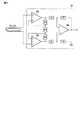
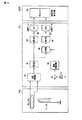
図8はタッチパネルコントローラIC2内の具体的な回路図の一例である。パルス発生器68の出力であるタッチ駆動信号TXがセレクタ92を介してTX駆動回路26又は遅延調整回路94に供給される。セレクタ92の切り替えはプロセッサ66の制御により行われる。セレクタ92は磁界発生期間TGTにTX駆動回路26に接続され、磁界検出期間TDTに遅延調整回路94に接続される。送信コイルTX_COILは一端子がTX駆動回路26に接続され、他端子が接地される。受信コイルRX_COILの両端子が差動増幅器82の2つの入力端子に接続される。図8では送信コイルTX_COILと受信コイルRX_COILは1つしか示されていないが、実際にはTX駆動回路26には多数の送信コイルTX_COILが接続され、多数の受信コイルRX_COILが多数の差動増幅器82にそれぞれ接続される。 FIG. 8 is an example of a specific circuit diagram in the touch panel controller IC2. The touch drive signal TX, which is the output of the
図9は差動増幅器82の回路図の一例である。差動増幅器82は3つの演算増幅器102、104、106と7個の抵抗R1〜R7からなる。2つの演算増幅器102、104が入力段に接続され、受信コイルRX_COILの一端子の信号が演算増幅器102の非反転入力端子に入力され、他端子の信号が演算増幅器104の非反転入力端子に入力される。演算増幅器102、104の出力端子間に3つの抵抗R2、R1、R3が直列に接続される。抵抗R1とR2の接続点が演算増幅器102の反転入力端子に入力され、抵抗R1とR3の接続点が演算増幅器104の反転入力端子に入力される。演算増幅器102の出力端子が抵抗R6を介して演算増幅器106の反転入力端子に接続され、演算増幅器104の出力端子が抵抗R4を介して演算増幅器106の非反転入力端子に接続される。演算増幅器106の出力端子が抵抗R7を介して演算増幅器106の反転入力端子に接続される。演算増幅器106の非反転入力端子が抵抗R5を介して接地される。演算増幅器106の出力が差動増幅器82の出力となる。 FIG. 9 is an example of a circuit diagram of the
抵抗R6と抵抗R4の抵抗値が等しく、抵抗R7と抵抗R5の抵抗値が等しいとすると、演算増幅器106の出力Voは下記で表される。Vpは正相信号、Vnは逆相信号である。
Vo=(R7/R6)(1+((R2+R3)/R1))(Vp−Vn)
各受信コイルRX_COILの両端子の信号が差動増幅器82の両入力端子にそれぞれ入力される。受信コイルRX_COILには図4で示したようにペン内コイルL1からの磁束の変動による誘起電圧以外にも外乱ノイズによる電圧も生じる。誘起電圧は受信コイルRX_COILの両端子で逆相の信号となるが、外乱ノイズによる電圧は両端子で同相の信号となる。そのため、受信コイルRX_COILの両端子の信号を差動増幅器82で増幅すると、外乱ノイズ成分は打ち消されて、誘起電圧成分のみが増幅される。差動増幅器82は、正相信号と逆相信号の振幅の絶対値の和の信号を増幅して出力する。Assuming that the resistance values of the resistors R6 and R4 are equal and the resistance values of the resistors R7 and R5 are equal, the output Vo of the
Vo = (R7 / R6) (1+ ((R2 + R3) / R1)) (Vp-Vn)
The signals of both terminals of each receiving coil RX_COIL are input to both input terminals of the
初段の差動増幅器82の出力が次段の増幅器84によりさらに増幅される。初段の差動増幅器82でノイズが除去されているので、次段の増幅器84は増幅率を高くすることができる。このため、微小なセンサ信号からでも、精度良くタッチ検出を行うことができる。 The output of the first-
増幅器84の出力が整流器86で整流、例えば半波整流される。整流器86の出力が積分器88に入力され、センサ信号が累積される。積分器88の出力がA/D変換器90によりデジタル信号とされてからプロセッサ66に供給される。プロセッサ66はA/D変換器90の出力デジタル信号がある閾値以上の場合、タッチを検出する。なお、センサ信号の累積値のヒステリシス特性を考慮して、非タッチからタッチへの変化を検出する閾値と、タッチから非タッチへの変化を検出する閾値とを異なる値としてもよい。 The output of the
ペンが表示装置1へ押し付けられる力によってコイルL1のインダクタンス、キャパシタンスが変化し、共振周波数が変わる。共振周波数の変化に応じてコイルL1の発する磁界も変化し、コイルL2に生じる誘起電圧の位相が変化する。検出回路62がタッチ駆動信号TXに対するセンサ信号の位相を検出すれば、筆圧も検出可能である。このため、パルス発生器68から出力されるタッチ駆動信号TXが遅延調整回路94を介して比較器96の第2入力端子に供給される。共振周波数が変化しなくても、差動増幅器82と増幅器84においてセンサ信号は位相がずれる。遅延調整回路94は、差動増幅器82と増幅器84におけるこの位相ずれを補償するものであり、タッチ駆動信号TXの位相を差動増幅器82と増幅器84における位相ずれと同じ量だけずらす。これにより、比較器96は整流回路86の出力のうちタッチ駆動信号TXと同じ位相成分のみを抽出するので、タッチ駆動信号TXに対するセンサ信号の位相差を検出することができる。 The inductance and capacitance of the coil L1 change due to the force with which the pen is pressed against the display device 1, and the resonance frequency changes. The magnetic field generated by the coil L1 also changes according to the change in the resonance frequency, and the phase of the induced voltage generated in the coil L2 changes. If the
比較器96の出力である位相差検知信号が積分器98に入力され、位相差検知信号が累積される。積分器98の出力がA/D変換器100によりデジタル信号とされてからプロセッサ66に供給される。プロセッサ66はA/D変換器100の出力デジタル信号に応じて筆圧を検出する。なお、センサ信号の累積値のヒステリシス特性を考慮して、筆圧大から小への変化を検出する閾値と、筆圧小から大への変化を検出する閾値とを異なる値としてもよい。筆圧を検出すると、タッチ検出した座標の軌跡に基づき手書き文字を表示する際、筆圧に応じて文字の太さを変えることができ、タッチパネルの使い勝手が向上する。 The phase difference detection signal, which is the output of the
[実施形態の纏め]
第1実施形態によれば、受信コイルRX_COILの両端子が差動増幅器82の2つの入力端子に接続される。ペン内コイルL1が発生する磁界の変化に応じて受信コイルRX_COILの両端子には互いに逆相の誘起電圧が生じる。受信コイルRX_COILの両端子の信号が差動増幅器82により増幅されるので、受信コイルRX_COILの両端子に生じる同相の外乱ノイズによる電圧は打ち消され、受信コイルRX_COILの両端子に生じる互いに逆相の誘起電圧のみ増幅される。このため、受信コイルRX_COILの両端子に生じる信号の振幅が微小であっても、誘起電圧成分のみを増幅し、検出感度を高めることができる。さらに、第1実施形態によれば、タッチ駆動信号TXに対するセンサ信号の位相差も検出することができるので、筆圧も検出することができる。[Summary of embodiments]
According to the first embodiment, both terminals of the receiving coil RX_COIL are connected to the two input terminals of the
[第2実施形態]
第1実施形態は近接(空中)と接触とを区別しないで両者をタッチとして検出したが、近接時と接触時とではセンサ信号のレベルがかなり違う場合がある。そのため、接触検出時のセンサ信号がA/D変換器90、100のダイナミックレンジを超える場合がある。[Second Embodiment]
In the first embodiment, both are detected as touches without distinguishing between proximity (in the air) and contact, but the level of the sensor signal may be considerably different between the proximity and the contact. Therefore, the sensor signal at the time of contact detection may exceed the dynamic range of the A /
第2実施形態では、タッチ検出モードとして近接検出モード(ホバーモードとも称する)と接触検出モード(ペンモードとも称する)とを備え、センサ信号に応じて両者のいずれかが選択的に設定される。ペンは表示装置に近づく場合、接触する前に先ず近接し、その後接触する。そのため、先ず初期時にホバーモードが設定され、ペンの近接が判定される。ホバーモード時にセンサ信号が第1閾値より高くなったら、ペンが表示装置に非常に近接したと判断でき、検出モードがペンモードに切り替わる。第1閾値は、A/D変換器90のビット数が10ビット(0〜1023)の場合、例えばダイナミックレンジの75%(≒768)でもよい。そして、ペンモード時にセンサ信号が第2閾値より低くなったら、ペンが表示装置から離れたと判断でき、検出モードがホバーモードに切り替わる。第2閾値は、例えばダイナミックレンジの25%(≒256)でもよい。 In the second embodiment, the touch detection mode includes a proximity detection mode (also referred to as a hover mode) and a contact detection mode (also referred to as a pen mode), and one of the two is selectively set according to the sensor signal. When the pen approaches the display device, it first approaches before contact and then contacts. Therefore, the hover mode is first set at the initial stage, and the proximity of the pen is determined. When the sensor signal becomes higher than the first threshold value in the hover mode, it can be determined that the pen is very close to the display device, and the detection mode is switched to the pen mode. When the number of bits of the A /
第2実施形態では、設定された検出モードに応じて検出回路62のゲインが切り替えられる。例えば、図10に示すように、差動増幅器82Aは、自身のゲインを高ゲインと低ゲインに切替えることができるスイッチ104を備える。スイッチ104は図9に示す抵抗R1、R2、R3、R6又はR7の抵抗値を変えるものであり、プロセッサ66により切り替えが制御される。他の構成は第1実施形態と同じである。 In the second embodiment, the gain of the
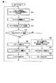
図11は第2実施形態の動作例を示すフローチャートである。ステップS12で、プロセッサ66はホバーモードを実行するために差動増幅器82Aのゲインを高ゲインに設定する。ホバーモード時のセンサ信号は比較的小さいので、検出回路62により高ゲインで増幅されても、増幅後のセンサ信号はA/D変換器90、100のダイナミックレンジ内に収まる。ステップS14で、プロセッサ66は、A/D変換器90の出力に基づいてペンの近接の有無を判断し、検出したペンの座標データを求める。近接検出の閾値はモード切替のための第1、第2閾値の中間の第3閾値(例えば、ダイナミックレンジの50%(=512))である。 FIG. 11 is a flowchart showing an operation example of the second embodiment. In step S12, the
ステップS16で、ホストプロセッサ66はA/D変換器90の出力が第1閾値以上であるか否か判定する。A/D変換器90の出力信号が第1閾値以上でない場合(ステップS16のNO)、ペンは表示装置から離れていると判断でき、プロセッサ66はステップS14の近接検出処理を繰り返す。A/D変換器90の出力信号が第1閾値以上である場合(ステップS16のYES)、ペンは表示装置にかなり近接していると判断でき、プロセッサ66は、ステップS18で、モードを切替え、ペンモードを実行するために差動増幅器82Aのゲインを低ゲインに設定する。ペンモード時のセンサ信号は大きいので、検出回路62により低ゲインで増幅されても、増幅後のセンサ信号はホバーモード時のセンサ信号と略等しく、A/D変換器90、100のダイナミックレンジ内に収まる。ステップS20で、ホストプロセッサ66は、A/D変換器90の出力に基づいてペンの接触の有無を検出し、接触したペンの座標データを求める。接触検出の閾値はモード切替のための第1、第2閾値の中間の第4閾値であり、ホバーモード時の近接検出のための第3閾値と同じでもよいし、異なっていてもよい。 In step S16, the
ステップS22で、プロセッサ66はA/D変換器90の出力が第2閾値以上であるか否か判定する。A/D変換器90の出力信号が第2閾値以上である場合(ステップS22のYES)、ペンは表示装置にかなり接近していると判断でき、ホストプロセッサ66はステップS20の接触検出処理を繰り返す。A/D変換器90の出力信号が第2閾値以上でない場合(ステップS22のNO)、ペンは表示装置から離れていると判断でき、プロセッサ66はステップS12に戻り、検出モードをホバーモードに切替える。 In step S22, the
[第2実施形態の纏め]
第2実施形態によれば、センス信号に基づいてペンが表示装置から離れているか又はかなり近づいているかが判断され、判断結果に応じて検出回路の差動増幅器のゲインが切り替えられる。このため、接触時にセンサ信号がA/D変換器のダイナミックレンジを超えることがなく、ホバーモードとペンモードの2つの検出モードの両方において好適にタッチ検出が行える。差動増幅器のゲインは差動増幅器の抵抗を切り替えることにより簡単に切替えることができる。なお、ゲインを高低の2レベル間で切替えたが、閾値を2つ以上設けて、より多いレベル間で切替えてもよい。
[第3実施形態]
上述の実施形態は電磁誘導方式のタッチ検出に関するが、静電容量方式のタッチ検出も可能な第3実施形態を説明する。[Summary of the second embodiment]
According to the second embodiment, it is determined whether the pen is away from or considerably close to the display device based on the sense signal, and the gain of the differential amplifier of the detection circuit is switched according to the determination result. Therefore, the sensor signal does not exceed the dynamic range of the A / D converter at the time of contact, and touch detection can be suitably performed in both the hover mode and the pen mode. The gain of the differential amplifier can be easily switched by switching the resistance of the differential amplifier. Although the gain is switched between two levels, high and low, two or more threshold values may be provided to switch between more levels.
[Third Embodiment]
Although the above-described embodiment relates to the touch detection of the electromagnetic induction method, the third embodiment in which the touch detection of the capacitance method is also possible will be described.
図12は第3実施形態の回路図の一例である。送信コイルTX_COILの一端子がスイッチ112を介して接地される。スイッチ112がオンの場合、送信コイルTX_COILの一端子が接地され、スイッチ112がオフの場合、送信コイルTX_COILの一端子はフローティング状態とされる。スイッチ112はプロセッサ66により制御される。送信コイルTX_COILの他端子はTX駆動回路26に接続される。 FIG. 12 is an example of a circuit diagram of the third embodiment. One terminal of the transmission coil TX_COIL is grounded via the
受信コイルRX_COILと差動増幅器82の間にスイッチ回路110が接続される。スイッチ回路110は第1スイッチ110aと第2スイッチ110bとを備える。第1スイッチ110aの入力端子はRX_COILの一端子(例えば正相信号側の端子子)に接続され、第1スイッチ110aの第1出力端子は差動増幅器82の第1入力端子(図9の演算増幅器102の非反転入力端子)に接続され、第1スイッチ110aの第2出力端子は積分器88に接続される。第2スイッチ110bの入力端子はRX_COILの他端子(例えば逆相信号側の端子)に接続され、第2スイッチ110bの第1出力端子は第1スイッチ110aの入力端子に接続され、第2スイッチ110bの第2出力端子は差動増幅器82の第2入力端子(図9の演算増幅器104の非反転入力端子)に接続される。第1スイッチ110a、第2スイッチ110bの切り替えはプロセッサ66により制御される。第1スイッチ110a、第2スイッチ110bは連動され、第1スイッチ110aが第1出力端子側に切替えられる時は第2スイッチ110bも第1出力端子側に切替えられ、第1スイッチ110aが第2出力端子側に切替えられる時は第2スイッチ110bも第2出力端子側に切替えられる。他の構成は第1実施形態と同じである。 The
第2スイッチ110bが第2出力側に接続されると、検出コイルRX_COILの両端子は短絡される。この時、第1スイッチ110aも第2出力端子側に接続されるので、検出コイルRX_COILの出力信号は積分回路88で積分される。この時、スイッチ112をオフして送信コイルTX_COILの一端子はフローティング状態とすると、送信コイルTX_COILに電流が流れず、送信コイルTX_COILは磁界を発生しない。そのため、受信コイルRX_COILはコイルではなく単なる導体となり、この導体によりユーザの指のタッチによる静電容量の変化が検出でき、検出回路62は静電容量式のタッチ検出を行う。 When the
第1、第2スイッチ110a、110bが第1出力側に接続されると、検出コイルRX_COILの両端子は差動増幅器82の2つの入力端子にそれぞれ接続され、検出器62は第1、第2実施形態と同様に電磁誘導方式のタッチ検出を行う。
図13は図12の回路構成を利用して電磁誘導方式と静電容量方式を動的に切替える動作の一例を示す。便宜上、電磁誘導方式のタッチ検出をペンモードと称し、静電容量方式のタッチ検出を指モードと称する。When the first and
FIG. 13 shows an example of an operation of dynamically switching between the electromagnetic induction method and the capacitance method using the circuit configuration of FIG. For convenience, the electromagnetic induction type touch detection is referred to as a pen mode, and the capacitance type touch detection is referred to as a finger mode.
タッチパネルでは表示とタッチ検出が交互に繰り返されるが、図13は1つのタッチ検出期間の動作を示す。ステップS32で、プロセッサ66はペンモードを実行するためにスイッチ回路110を第1出力端子側に切替え、検出コイルRX_COILの両端子を差動増幅器82の2つの入力端子にそれぞれ接続させる。ステップS34で、ホストプロセッサ66はスイッチ112をオンし、TX駆動回路26からの駆動信号TXを送信コイルRX_COILに流す。この時、略全部の駆動電極TLが互いに接続され、1つの大きい送信コイルTX_COILが形成され、送信コイルTX_COILが全面駆動される。送信コイルTX_COILが発生する磁界はコイルの大きさに比例するので、全面駆動により発生される磁界の方が順次スキャン駆動により発生される磁界より大きい。このため、ペンの近接を感度よく検知することができる。なお、第2実施形態で説明したように、ペンは先ず近接し、その後接触するので、全面駆動の際、差動増幅器82を第2実施形態の差動増幅器82Aにして、そのゲインを高ゲインにしてもよい。 On the touch panel, display and touch detection are alternately repeated, and FIG. 13 shows the operation during one touch detection period. In step S32, the
ステップS36でプロセッサ66は各検出器62の出力をA/D変換器64を介して受信する。ステップS38でプロセッサ66はいずれかの検出結果が閾値以上であるか否かを判定する。この閾値はA/D変換器90のビット数が10ビット(0〜1023)の場合、例えばダイナミックレンジの25%(≒256)でもよい。いずれか1つの検出結果でも閾値以上である場合、プロセッサ66はペンが近接状態にあると判断でき、ステップS42でペンモードを実行するためにスイッチ回路110を第1出力端子側に切替え、検出コイルRX_COILの両端子を差動増幅器82の2つの入力端子にそれぞれ接続させる。ステップS44で、プロセッサ66はスイッチ112をオンし、TX駆動回路26からの駆動信号TXを送信コイルRX_COILに流す。この時、駆動電極TLは数本ずつが互いに接続され、多数の送信コイルTX_COILが形成され、多数の送信コイルTX_COILが順次スキャン駆動される。全面駆動の際差動増幅器82のゲインを高ゲインにした場合は、スキャン駆動の際差動増幅器82のゲインを低ゲインにする。 In step S36, the
ステップS46でプロセッサ66は各検出器62の出力をA/D変換器64を介して受信し、ペンのタッチを検出し、ペンのタッチ位置を表すペンデータを出力する。1つのタッチ検出期間が終了すると、表示期間を経て次のタッチ検出期間になると、ステップS32に戻る。 In step S46, the
ステップS38でいずれかの検出結果も閾値以上ではない場合、プロセッサ66はペンが近接状態ではないと判断でき、ステップS48で指モードを実行するためにスイッチ回路110を第2出力端子側に切替え、検出コイルRX_COILの両端子を短絡し、検出コイルRX_COILを積分器88に接続する。ステップS52で、プロセッサ66はスイッチ112をオンし、TX駆動回路26からの駆動信号TXを送信コイルRX_COILに流す。この時、駆動電極TLは数本ずつが互いに接続され、多数の送信コイルTX_COILが形成され、多数の送信コイルTX_COILが順次スキャン駆動される。全面駆動の際差動増幅器82のゲインを高ゲインにした場合は、スキャン駆動の際差動増幅器82のゲインを低ゲインにする。 If any of the detection results is not equal to or higher than the threshold value in step S38, the
ステップS52でプロセッサ66は各検出器62の出力をA/D変換器64を介して受信し、指のタッチを検出し、指のタッチ位置を表す指データを出力する。1つのタッチ検出期間が終了すると、表示期間を経て次のタッチ検出期間になると、ステップS32に戻る。 In step S52, the
[第3実施形態の纏め]
第3実施形態によれば、受信コイルRX_COILの両端を選択的に短絡するスイッチ回路110を設けることにより、受信コイルRX_COILをコイルではなく導体として機能させることができ、静電容量方式のタッチ検出も可能である。スイッチ回路110によりコイルの受信コイルRX_COILの両端を差動増幅器82の2つの入力端子に接続させることもでき、電磁誘導方式のタッチ検出も可能である。さらに、略全部の駆動電極TLを互いに接続し、1つの大きい送信コイルTX_COILを形成し、送信コイルTX_COILを全面駆動した時の受信コイルRX_COILの出力レベルに基づいてペンモードと指モードを自動的に切替えることができる。[Summary of the third embodiment]
According to the third embodiment, by providing the
[レイアウト例]
図14、図15は上述の実施形態の各回路のレイアウト例を示す。図14では、送信コイルTX_COILと受信コイルRX_COILをタッチパネルPNLに設け、プロセッサ66をホスト装置HOSTに設け、それ以外をタッチパネルコントローラIC2に設ける。図14では差動増幅器82から出力された受信コイルRX_COILの誘起電圧を表すアナログ信号がタッチパネルコントローラIC2内で整流、比較、積分等の処理をされ近接又は接近を表すデジタルデータとしてプロセッサ66に入力される。[Layout example]
14 and 15 show layout examples of each circuit of the above-described embodiment. In FIG. 14, the transmission coil TX_COIL and the reception coil RX_COIL are provided on the touch panel PNL, the
図15は、送信コイルTX_COILと受信コイルRX_COILをタッチパネルPNLに設け、プロセッサ66をホスト装置HOSTに設け、それ以外をタッチパネルコントローラIC2に設ける。図14の例とは異なり図15の例では、タッチパネルコントローラIC2は整流、比較、積分等の処理を行わず、受信コイルRX_COILの出力波形が単にA/D変換されデジタル波形データとしてプロセッサ66に入力される。プロセッサ66がデジタルデータに基づいて整流、比較、積分等の処理を行う。また、受信信号と駆動信号との位相差を検出するために、駆動信号もA/D変換器144を介してデジタルデータとしてプロセッサ66に入力される。図15の例では、タッチパネルコントローラIC2の構成が簡略化され、消費電力が少ない。 In FIG. 15, the transmission coil TX_COIL and the reception coil RX_COIL are provided on the touch panel PNL, the
なお、本発明は上記実施形態そのままに限定されるものではなく、実施段階ではその要旨を逸脱しない範囲で構成要素を変形して具体化できる。また、上記実施形態に開示されている複数の構成要素の適宜な組み合せにより種々の発明を形成できる。例えば、実施形態に示される全構成要素から幾つかの構成要素を削除してもよい。更に、異なる実施形態に亘る構成要素を適宜組み合せてもよい。 The present invention is not limited to the above embodiment as it is, and at the implementation stage, the components can be modified and embodied within a range that does not deviate from the gist thereof. In addition, various inventions can be formed by an appropriate combination of the plurality of components disclosed in the above-described embodiment. For example, some components may be removed from all the components shown in the embodiments. In addition, components from different embodiments may be combined as appropriate.
TL…駆動電極、SL…信号線、TX_COIL…送信コイル、RX_COIL…受信コイル、26…TX駆動回路、62…検出回路、66…プロセッサ、82…差動増幅器、86…整流器、88,98…積分器、90,100…A/D変換器、94…遅延調整回路、96…比較器。 TL ... drive electrode, SL ... signal line, TX_COIL ... transmit coil, RX_COIL ... receive coil, 26 ... TX drive circuit, 62 ... detection circuit, 66 ... processor, 82 ... differential amplifier, 86 ... rectifier, 88,98 ... integrator Integrator, 90, 100 ... A / D converter, 94 ... Delay adjustment circuit, 96 ... Comparator.
Claims (17)
Translated fromJapanese前記受信コイルの両端が接続される2つの入力端子を具備する差動増幅器と、
前記送信コイルに供給された駆動信号と、前記差動増幅器の出力信号との位相差を検出する比較器と、
前記差動増幅器の位相遅延を補償する補償回路と、を具備し、
前記駆動信号は前記補償回路を介して前記比較器に入力される、タッチ検出装置。A touch panel equipped with a transmitting coil and a receiving coil, and having a display function and a touch detection function,
A differential amplifier having two input terminals to which both ends of the receiving coil are connected,
A comparator that detects the phase difference between the drive signal supplied to the transmission coil and the output signal of the differential amplifier, and
A compensation circuit for compensating for the phase delay of the differential amplifier is provided.
A touch detection devicein which the drive signal is input to the comparator via the compensation circuit.
前記第1演算増幅器の出力端子が前記第3演算増幅器の反転入力端子に接続され、
前記第2演算増幅器の出力端子が前記第3演算増幅器の非反転入力端子に接続され、
前記第1演算増幅器の反転入力端子と前記第2演算増幅器の反転入力端子が互いに接続され、
前記受信コイルの一端が前記第1演算増幅器の非反転入力端子に接続され、
前記受信コイルの他端が前記第2演算増幅器の非反転入力端子に接続される請求項1記載のタッチ検出装置。The differential amplifier includes a first operational amplifier, a second operational amplifier, and a third operational amplifier.
The output terminal of the first operational amplifier is connected to the inverting input terminal of the third operational amplifier.
The output terminal of the second operational amplifier is connected to the non-inverting input terminal of the third operational amplifier.
The inverting input terminal of the first operational amplifier and the inverting input terminal of the second operational amplifier are connected to each other.
One end of the receiving coil is connected to the non-inverting input terminal of the first operational amplifier.
The touch detection device according to claim 1, wherein the other end of the receiving coil is connected to a non-inverting input terminal of the second operational amplifier.
前記第2演算増幅器の出力端子が第2抵抗を介して前記第2演算増幅器の反転入力端子に接続され、
前記第1抵抗と前記第2抵抗の間に第3抵抗が接続され、
前記第1演算増幅器の出力端子が第4抵抗を介して前記第3演算増幅器の反転入力端子に接続され、
前記第2演算増幅器の出力端子が第5抵抗を介して前記第3演算増幅器の非反転入力端子に接続され、
前記第3演算増幅器の出力端子が第6抵抗を介して前記第3演算増幅器の反転入力端子に接続され、
前記第3演算増幅器の非反転入力端子が第7抵抗を介して接地され、
前記第1抵抗、前記第2抵抗、前記第3抵抗、前記第4抵抗、前記第5抵抗、前記第6抵抗、前記第7抵抗のうちの1つまたは複数の抵抗値を変えることにより、前記差動増幅器のゲインを変更するゲイン調整手段をさらに具備する請求項2記載のタッチ検出装置。The output terminal of the first operational amplifier is connected to the inverting input terminal of the first operational amplifier via the first resistor.
The output terminal of the second operational amplifier is connected to the inverting input terminal of the second operational amplifier via a second resistor.
A third resistor is connected between the first resistor and the second resistor,
The output terminal of the first operational amplifier is connected to the inverting input terminal of the third operational amplifier via a fourth resistor.
The output terminal of the second operational amplifier is connected to the non-inverting input terminal of the third operational amplifier via a fifth resistor.
The output terminal of the third operational amplifier is connected to the inverting input terminal of the third operational amplifier via a sixth resistor.
The non-inverting input terminal of the third operational amplifier is grounded via the seventh resistor.
By changing the resistance value of one or more of the first resistance, the second resistance, the third resistance, the fourth resistance, the fifth resistance, the sixth resistance, and the seventh resistance. The touch detection device according to claim 2, further comprising a gain adjusting means for changing the gain of the differential amplifier.
前記差動増幅器の出力レベルが第1閾値以上の場合の場合低ゲインを選択し、
前記差動増幅器の出力レベルが第1閾値以下の第2閾値以下の場合前記低ゲインより高い高ゲインを選択する請求項4記載のタッチ検出装置。The gain adjusting means is
When the output level of the differential amplifier is equal to or higher than the first threshold value, low gain is selected.
The touch detection device according to claim 4, wherein when the output level of the differential amplifier is equal to or less than the first threshold and equal to or less than the second threshold, a high gain higher than the low gain is selected.
前記スイッチ回路は、第1状態では前記受信コイルの両端を前記差動増幅器の2つの入力端子に接続させ、第2状態では前記受信コイルの両端を短絡させ、前記差動増幅器に接続させない請求項1乃至請求項5のいずれか一項記載のタッチ検出装置。A switch circuit connected to both ends of the receiving coil is further provided.
A claim that the switch circuit connects both ends of the receiving coil to the two input terminals of the differential amplifier in the first state, short-circuits both ends of the receiving coil in the second state, and does not connect to the differential amplifier. The touch detection device according to any one of 1 to 5.
X方向とY方向の2次元アレイ状に配列された複数の画素と、
X方向に並ぶ画素行毎に接続されるX方向に延びる複数の駆動電極と、
Y方向に並ぶ画素列毎に接続されるY方向に延びる複数の信号線と、を具備し
前記送信コイルは前記複数の駆動電極からなり、
前記受信コイルは前記複数の信号線からなる請求項1乃至請求項7のいずれか一項記載のタッチ検出装置。The touch panel has a plurality of pixels arranged in a two-dimensional array in the X direction and the Y direction, and
A plurality of drive electrodes extending in the X direction connected to each pixel row arranged in the X direction,
The transmission coil includes a plurality of signal lines extending in the Y direction connected to each pixel row arranged in the Y direction, and the transmission coil is composed of the plurality of drive electrodes.
The touch detection device according to any one of claims 1 to 7, wherein the receiving coil is composed of the plurality of signal lines.
前記複数の画素が形成される第1基板と、
前記第1基板の上に配置され、カラーフィルタが形成される第2基板と、
前記第1基板と前記第2基板の間に配置される液晶層と、を具備し、
前記複数の駆動電極は前記第1基板に形成され、前記複数の信号線は前記第2基板に形成される請求項8記載のタッチ検出装置。The touch panel includes a first substrate on which the plurality of pixels are formed, and the touch panel.
A second substrate arranged on the first substrate and on which a color filter is formed, and a second substrate.
A liquid crystal layer arranged between the first substrate and the second substrate is provided.
The touch detection device according to claim 8, wherein the plurality of drive electrodes are formed on the first substrate, and the plurality of signal lines are formed on the second substrate.
前記複数の画素が形成される第1基板と、
前記第1基板の上に配置され、カラーフィルタが形成される第2基板と、
前記第1基板と前記第2基板の間に配置される液晶層と、を具備し、
前記複数の信号線は前記第1基板に形成され、前記複数の駆動電極は絶縁層を介して前記複数の信号線の上に形成される請求項8記載のタッチ検出装置。The touch panel includes a first substrate on which the plurality of pixels are formed, and the touch panel.
A second substrate arranged on the first substrate and on which a color filter is formed, and a second substrate.
A liquid crystal layer arranged between the first substrate and the second substrate is provided.
The touch detection device according to claim 8, wherein the plurality of signal lines are formed on the first substrate, and the plurality of drive electrodes are formed on the plurality of signal lines via an insulating layer.
前記ICチップの出力はホスト装置に送信され、前記ホスト装置で前記A/D変換器の出力に基づいてタッチ位置の座標を計算させる請求項1乃至請求項10のいずれか一項記載のタッチ検出装置。An IC chip including the differential amplifier, a rectifier that rectifies the output of the differential amplifier, an integrator that integrates the output of the rectifier, and an A / D converter that converts the output of the integrator into a digital signal. Further equipped,
The touch detection according to any one of claims 1 to 10, wherein the output of the IC chip is transmitted to the host device, and the host device calculates the coordinates of the touch position based on the output of the A / D converter. apparatus.
前記ICチップの出力はホスト装置に送信され、前記ホスト装置で前記A/D変換器の出力を整流させ、整流結果を積分させ、積分結果に基づいてタッチ位置の座標を計算させる請求項1乃至請求項10のいずれか一項記載のタッチ検出装置。An IC chip including the differential amplifier and an A / D converter that converts the output of the differential amplifier into a digital signal is further provided.
The output of the IC chip is transmitted to a host device, the output of the A / D converter is rectified by the host device, the rectification result is integrated, and the coordinates of the touch position are calculated based on the integration result. The touch detection device according to any one of claim 10.
前記送信コイルに供給された駆動信号の位相を前記差動増幅器の位相遅延に応じてずらし、
前記差動増幅器の出力信号と前記位相がずらされた前記送信コイルに供給された駆動信号との位相差を検出するタッチ検出方法。A differential amplifier is used to amplify the signals induced at both ends of the receiving coil of the touch panel, whichhas a transmitting coil and a receiving coil, and has adisplay function and a touch detection function.
The phase of the drive signal supplied to the transmission coil is shifted according to the phase delay of the differential amplifier.
A touch detection methodfor detecting a phase difference between an output signal of the differential amplifier and a drive signal supplied to the transmission coil whose phase is shifted.
前記差動増幅器の出力レベルが第1閾値以下の第2閾値以下の場合前記低ゲインより高い高ゲインを選択する請求項13記載のタッチ検出方法。When the output level of the differential amplifier is equal to or higher than the first threshold value, low gain is selected.
The touch detection method according to claim 13, wherein when the output level of the differential amplifier is equal to or less than the first threshold and equal to or less than the second threshold, a high gain higher than the low gain is selected.
Priority Applications (2)
| Application Number | Priority Date | Filing Date | Title |
|---|---|---|---|
| JP2017085167AJP6900231B2 (en) | 2017-04-24 | 2017-04-24 | Touch detection device and method |
| US15/959,699US10545589B2 (en) | 2017-04-24 | 2018-04-23 | Touch detection device |
Applications Claiming Priority (1)
| Application Number | Priority Date | Filing Date | Title |
|---|---|---|---|
| JP2017085167AJP6900231B2 (en) | 2017-04-24 | 2017-04-24 | Touch detection device and method |
Publications (2)
| Publication Number | Publication Date |
|---|---|
| JP2018185559A JP2018185559A (en) | 2018-11-22 |
| JP6900231B2true JP6900231B2 (en) | 2021-07-07 |
Family
ID=63852351
Family Applications (1)
| Application Number | Title | Priority Date | Filing Date |
|---|---|---|---|
| JP2017085167AActiveJP6900231B2 (en) | 2017-04-24 | 2017-04-24 | Touch detection device and method |
Country Status (2)
| Country | Link |
|---|---|
| US (1) | US10545589B2 (en) |
| JP (1) | JP6900231B2 (en) |
Cited By (1)
| Publication number | Priority date | Publication date | Assignee | Title |
|---|---|---|---|---|
| US11861107B2 (en) | 2022-03-10 | 2024-01-02 | Samsung Display Co., Ltd. | Input sensing part and driving method thereof |
Families Citing this family (12)
| Publication number | Priority date | Publication date | Assignee | Title |
|---|---|---|---|---|
| JP7109201B2 (en)* | 2018-01-29 | 2022-07-29 | 株式会社ワコム | A method performed by a pen or pen detection device for detecting said pen |
| US10997882B2 (en)* | 2018-07-23 | 2021-05-04 | Samsung Electronics Co., Ltd. | Short detection device, a short detection circuit and a display device using the same |
| DE102019104385A1 (en)* | 2019-02-21 | 2020-08-27 | Polyic Gmbh & Co. Kg | Sensor substrate with electronics and use for it |
| JP2020187427A (en)* | 2019-05-10 | 2020-11-19 | 株式会社ジャパンディスプレイ | Sensor device |
| JP2021086368A (en)* | 2019-11-27 | 2021-06-03 | シャープ株式会社 | Electronic apparatus |
| US11983364B2 (en) | 2020-01-22 | 2024-05-14 | Hideep Inc. | Stylus pen, antenna module, touch sensor, and electronic device |
| CN113358013B (en)* | 2020-03-06 | 2023-03-28 | 深圳普赢创新科技股份有限公司 | Electromagnetic induction type coordinate positioning device |
| KR102804841B1 (en)* | 2020-07-15 | 2025-05-09 | 주식회사 엘엑스세미콘 | Touch Sensing Device for Compensating Phase Error of Active Pen and Method for Compensating Phase Error of Active Pen |
| JP7456018B2 (en)* | 2021-02-02 | 2024-03-26 | 株式会社ワコム | Sensor board and display device |
| CN115657884B (en)* | 2022-10-14 | 2025-07-22 | 武汉华星光电技术有限公司 | Electromagnetic touch screen and electromagnetic touch device |
| WO2025005066A1 (en)* | 2023-06-27 | 2025-01-02 | 株式会社ワコム | Position detection device and sensor |
| WO2025005138A1 (en)* | 2023-06-27 | 2025-01-02 | 株式会社ワコム | Position detection device and display device |
Family Cites Families (11)
| Publication number | Priority date | Publication date | Assignee | Title |
|---|---|---|---|---|
| JPH0282310A (en)* | 1988-09-19 | 1990-03-22 | Omron Tateisi Electron Co | Coordinate position detector |
| JP4955262B2 (en)* | 2004-12-07 | 2012-06-20 | サムスン エレクトロニクス カンパニー リミテッド | Illuminance control device for liquid crystal display device, light sensing element, and backlight source |
| JP5216495B2 (en)* | 2008-09-16 | 2013-06-19 | 株式会社ジャパンディスプレイウェスト | Contact detection device and display device |
| TWI417624B (en)* | 2009-11-19 | 2013-12-01 | Innolux Display Corp | Touch display device |
| WO2012056882A1 (en)* | 2010-10-27 | 2012-05-03 | 株式会社村田製作所 | Detection circuit |
| US8988384B2 (en)* | 2011-09-23 | 2015-03-24 | Apple Inc. | Force sensor interface for touch controller |
| US20150277601A1 (en)* | 2012-09-28 | 2015-10-01 | Kenji Tahara | Specified position detection device |
| WO2015125170A1 (en)* | 2014-02-18 | 2015-08-27 | ニューコムテクノ株式会社 | Pointed-to position detection device |
| JP6408415B2 (en) | 2015-03-31 | 2018-10-17 | 株式会社ジャパンディスプレイ | Display device |
| JP2016031767A (en)* | 2015-09-30 | 2016-03-07 | ニューコムテクノ株式会社 | Position detection unit |
| JP6605292B2 (en)* | 2015-10-16 | 2019-11-13 | 株式会社ジャパンディスプレイ | Display device |
- 2017
- 2017-04-24JPJP2017085167Apatent/JP6900231B2/enactiveActive
- 2018
- 2018-04-23USUS15/959,699patent/US10545589B2/enactiveActive
Cited By (1)
| Publication number | Priority date | Publication date | Assignee | Title |
|---|---|---|---|---|
| US11861107B2 (en) | 2022-03-10 | 2024-01-02 | Samsung Display Co., Ltd. | Input sensing part and driving method thereof |
Also Published As
| Publication number | Publication date |
|---|---|
| US20180307340A1 (en) | 2018-10-25 |
| JP2018185559A (en) | 2018-11-22 |
| US10545589B2 (en) | 2020-01-28 |
Similar Documents
| Publication | Publication Date | Title |
|---|---|---|
| JP6900231B2 (en) | Touch detection device and method | |
| US11847287B2 (en) | Touch panel, display panel, and display unit | |
| US10698506B2 (en) | Input system and method for detecting touch using the same | |
| US11693462B2 (en) | Central receiver for performing capacitive sensing | |
| US10551962B2 (en) | Touch detection device, display device with touch detection function, and covering member | |
| US10241597B2 (en) | Active stylus pen and touch sensing system including the same | |
| US10139952B2 (en) | Display apparatus and touch detection apparatus using shift of detection operation for reduced detection time | |
| US9426882B2 (en) | Flexible printed circuit for connecting touch screen and liquid crystal display device using the same | |
| CN107977107B (en) | Display device including touch sensor and touch sensing method thereof | |
| CN102446026B (en) | There is the display device of touch panel | |
| US8933898B2 (en) | Touch sensor integrated type display device | |
| KR101410414B1 (en) | Touch screen panel having function of sensing motion | |
| KR101756663B1 (en) | Apparatus and method for driving display panel with built-in touch sensor | |
| US10078393B2 (en) | Touch detection device, display device with touch detection function, and cover member | |
| CN107015697B (en) | display device | |
| WO2010137727A1 (en) | Touch sensor display and electronic device | |
| US11669203B2 (en) | Detection device | |
| KR101726633B1 (en) | Apparatus and method for driving touch sensor | |
| KR101839337B1 (en) | Apparatus and method for driving display panel with built-in touch sensor | |
| KR102192520B1 (en) | Touch screen device and method for driving thereof | |
| KR102506658B1 (en) | Touch screen device and its driving method | |
| CN112071248A (en) | Gate select signal with reduced glitch | |
| TWM649098U (en) | Touch display device | |
| JP2008268889A (en) | Liquid crystal device |
Legal Events
| Date | Code | Title | Description |
|---|---|---|---|
| A621 | Written request for application examination | Free format text:JAPANESE INTERMEDIATE CODE: A621 Effective date:20200326 | |
| A131 | Notification of reasons for refusal | Free format text:JAPANESE INTERMEDIATE CODE: A131 Effective date:20201222 | |
| A977 | Report on retrieval | Free format text:JAPANESE INTERMEDIATE CODE: A971007 Effective date:20201225 | |
| A521 | Request for written amendment filed | Free format text:JAPANESE INTERMEDIATE CODE: A523 Effective date:20210210 | |
| TRDD | Decision of grant or rejection written | ||
| A01 | Written decision to grant a patent or to grant a registration (utility model) | Free format text:JAPANESE INTERMEDIATE CODE: A01 Effective date:20210601 | |
| A61 | First payment of annual fees (during grant procedure) | Free format text:JAPANESE INTERMEDIATE CODE: A61 Effective date:20210616 | |
| R150 | Certificate of patent or registration of utility model | Ref document number:6900231 Country of ref document:JP Free format text:JAPANESE INTERMEDIATE CODE: R150 | |
| S111 | Request for change of ownership or part of ownership | Free format text:JAPANESE INTERMEDIATE CODE: R313113 | |
| R350 | Written notification of registration of transfer | Free format text:JAPANESE INTERMEDIATE CODE: R350 | |
| R250 | Receipt of annual fees | Free format text:JAPANESE INTERMEDIATE CODE: R250 | |
| R250 | Receipt of annual fees | Free format text:JAPANESE INTERMEDIATE CODE: R250 |