JP6898501B2 - Wafer defect detection system and method - Google Patents
Wafer defect detection system and methodDownload PDFInfo
- Publication number
- JP6898501B2 JP6898501B2JP2020114760AJP2020114760AJP6898501B2JP 6898501 B2JP6898501 B2JP 6898501B2JP 2020114760 AJP2020114760 AJP 2020114760AJP 2020114760 AJP2020114760 AJP 2020114760AJP 6898501 B2JP6898501 B2JP 6898501B2
- Authority
- JP
- Japan
- Prior art keywords
- wafer
- design
- defect
- defects
- process step
- Prior art date
- Legal status (The legal status is an assumption and is not a legal conclusion. Google has not performed a legal analysis and makes no representation as to the accuracy of the status listed.)
- Active
Links
Images


Classifications
- G—PHYSICS
- G01—MEASURING; TESTING
- G01N—INVESTIGATING OR ANALYSING MATERIALS BY DETERMINING THEIR CHEMICAL OR PHYSICAL PROPERTIES
- G01N21/00—Investigating or analysing materials by the use of optical means, i.e. using sub-millimetre waves, infrared, visible or ultraviolet light
- G01N21/84—Systems specially adapted for particular applications
- G01N21/88—Investigating the presence of flaws or contamination
- G01N21/95—Investigating the presence of flaws or contamination characterised by the material or shape of the object to be examined
- G01N21/9501—Semiconductor wafers
- G—PHYSICS
- G01—MEASURING; TESTING
- G01B—MEASURING LENGTH, THICKNESS OR SIMILAR LINEAR DIMENSIONS; MEASURING ANGLES; MEASURING AREAS; MEASURING IRREGULARITIES OF SURFACES OR CONTOURS
- G01B11/00—Measuring arrangements characterised by the use of optical techniques
- G01B11/14—Measuring arrangements characterised by the use of optical techniques for measuring distance or clearance between spaced objects or spaced apertures
- G—PHYSICS
- G01—MEASURING; TESTING
- G01N—INVESTIGATING OR ANALYSING MATERIALS BY DETERMINING THEIR CHEMICAL OR PHYSICAL PROPERTIES
- G01N21/00—Investigating or analysing materials by the use of optical means, i.e. using sub-millimetre waves, infrared, visible or ultraviolet light
- G01N21/84—Systems specially adapted for particular applications
- G01N21/88—Investigating the presence of flaws or contamination
- G01N21/95—Investigating the presence of flaws or contamination characterised by the material or shape of the object to be examined
- G01N21/956—Inspecting patterns on the surface of objects
- G—PHYSICS
- G03—PHOTOGRAPHY; CINEMATOGRAPHY; ANALOGOUS TECHNIQUES USING WAVES OTHER THAN OPTICAL WAVES; ELECTROGRAPHY; HOLOGRAPHY
- G03F—PHOTOMECHANICAL PRODUCTION OF TEXTURED OR PATTERNED SURFACES, e.g. FOR PRINTING, FOR PROCESSING OF SEMICONDUCTOR DEVICES; MATERIALS THEREFOR; ORIGINALS THEREFOR; APPARATUS SPECIALLY ADAPTED THEREFOR
- G03F7/00—Photomechanical, e.g. photolithographic, production of textured or patterned surfaces, e.g. printing surfaces; Materials therefor, e.g. comprising photoresists; Apparatus specially adapted therefor
- G03F7/70—Microphotolithographic exposure; Apparatus therefor
- G03F7/70425—Imaging strategies, e.g. for increasing throughput or resolution, printing product fields larger than the image field or compensating lithography- or non-lithography errors, e.g. proximity correction, mix-and-match, stitching or double patterning
- G03F7/70466—Multiple exposures, e.g. combination of fine and coarse exposures, double patterning or multiple exposures for printing a single feature
- G—PHYSICS
- G03—PHOTOGRAPHY; CINEMATOGRAPHY; ANALOGOUS TECHNIQUES USING WAVES OTHER THAN OPTICAL WAVES; ELECTROGRAPHY; HOLOGRAPHY
- G03F—PHOTOMECHANICAL PRODUCTION OF TEXTURED OR PATTERNED SURFACES, e.g. FOR PRINTING, FOR PROCESSING OF SEMICONDUCTOR DEVICES; MATERIALS THEREFOR; ORIGINALS THEREFOR; APPARATUS SPECIALLY ADAPTED THEREFOR
- G03F7/00—Photomechanical, e.g. photolithographic, production of textured or patterned surfaces, e.g. printing surfaces; Materials therefor, e.g. comprising photoresists; Apparatus specially adapted therefor
- G03F7/70—Microphotolithographic exposure; Apparatus therefor
- G03F7/70483—Information management; Active and passive control; Testing; Wafer monitoring, e.g. pattern monitoring
- G03F7/70605—Workpiece metrology
- G03F7/70616—Monitoring the printed patterns
- G03F7/70633—Overlay, i.e. relative alignment between patterns printed by separate exposures in different layers, or in the same layer in multiple exposures or stitching
- G—PHYSICS
- G03—PHOTOGRAPHY; CINEMATOGRAPHY; ANALOGOUS TECHNIQUES USING WAVES OTHER THAN OPTICAL WAVES; ELECTROGRAPHY; HOLOGRAPHY
- G03F—PHOTOMECHANICAL PRODUCTION OF TEXTURED OR PATTERNED SURFACES, e.g. FOR PRINTING, FOR PROCESSING OF SEMICONDUCTOR DEVICES; MATERIALS THEREFOR; ORIGINALS THEREFOR; APPARATUS SPECIALLY ADAPTED THEREFOR
- G03F7/00—Photomechanical, e.g. photolithographic, production of textured or patterned surfaces, e.g. printing surfaces; Materials therefor, e.g. comprising photoresists; Apparatus specially adapted therefor
- G03F7/70—Microphotolithographic exposure; Apparatus therefor
- G03F7/70483—Information management; Active and passive control; Testing; Wafer monitoring, e.g. pattern monitoring
- G03F7/70605—Workpiece metrology
- G03F7/70616—Monitoring the printed patterns
- G03F7/7065—Defects, e.g. optical inspection of patterned layer for defects
- H—ELECTRICITY
- H01—ELECTRIC ELEMENTS
- H01L—SEMICONDUCTOR DEVICES NOT COVERED BY CLASS H10
- H01L22/00—Testing or measuring during manufacture or treatment; Reliability measurements, i.e. testing of parts without further processing to modify the parts as such; Structural arrangements therefor
- H01L22/10—Measuring as part of the manufacturing process
- H01L22/12—Measuring as part of the manufacturing process for structural parameters, e.g. thickness, line width, refractive index, temperature, warp, bond strength, defects, optical inspection, electrical measurement of structural dimensions, metallurgic measurement of diffusions
Landscapes
- Physics & Mathematics (AREA)
- General Physics & Mathematics (AREA)
- Health & Medical Sciences (AREA)
- Life Sciences & Earth Sciences (AREA)
- Chemical & Material Sciences (AREA)
- Analytical Chemistry (AREA)
- Biochemistry (AREA)
- General Health & Medical Sciences (AREA)
- Immunology (AREA)
- Pathology (AREA)
- Engineering & Computer Science (AREA)
- Manufacturing & Machinery (AREA)
- Computer Hardware Design (AREA)
- Microelectronics & Electronic Packaging (AREA)
- Power Engineering (AREA)
- Testing Or Measuring Of Semiconductors Or The Like (AREA)
- Investigating Materials By The Use Of Optical Means Adapted For Particular Applications (AREA)
- Analysing Materials By The Use Of Radiation (AREA)
Description
Translated fromJapanese本発明は一般に、ウェーハに多プロセスステップが実行された後にウェーハを検査し、そのプロセスステップのうちいずれが、検査によって検出された欠陥に対応するかを判定するシステムおよび方法に関する。 The present invention generally relates to a system and method of inspecting a wafer after a multi-process step has been performed on the wafer and determining which of the process steps corresponds to a defect detected by the inspection.
以下の説明と例は、この部分に包含されることにより、従来技術とは認められない。 The following description and examples are not recognized as prior art by inclusion in this section.
検査プロセスは、半導体製造プロセスにおいてより高い歩留まりを促進し、したがってより高い利益を促進するために、半導体製造プロセス中の種々のステップでウェーハ上の欠陥を検出するために用いられる。半導体デバイスの組立てにおいて、検査は常に重要な部分であった。しかし、半導体デバイスの寸法が減少するにつれ、より小さい欠陥がデバイスを故障させ得るため、許容できる半導体デバイスの製造を成功させるために、検査は一層重要となっている。 Inspection processes are used to detect defects on wafers at various steps in the semiconductor manufacturing process in order to promote higher yields and thus higher profits in the semiconductor manufacturing process. Inspection has always been an important part of the assembly of semiconductor devices. However, as the dimensions of semiconductor devices decrease, smaller defects can cause the device to fail, making inspection even more important for the successful manufacture of acceptable semiconductor devices.
現在、各プロセスは、単一のプロセスステップを用いて、エクスカーションと性能に関して監視される。例えば、特定のプロセスステップ(例えば、化学気相成長(CVD)、成膜、エッチングまたは同様の製造ステップ)を経る可能性がある。次にウェーハは検査ツールに移送されて、欠陥とその他のプロセス関連事項に関して検査される。 Currently, each process is monitored for excursions and performance using a single process step. For example, it may go through certain process steps (eg, chemical vapor deposition (CVD), film formation, etching or similar manufacturing steps). The wafer is then transferred to an inspection tool and inspected for defects and other process related matters.
そのような例のうち一つにおいて、ウェーハは図7のステップ700に示すようにプロセスステップAで処理されてもよい。次にウェーハは、プロセスステップAを実行するプロセスツールから、ステップ702に示す検査/レビューAのための1つ以上の他のツール(検査および/またはレビューツール)に移送される。次にウェーハは、検査および/またはレビューツールから、ステップ704に示すプロセスステップBのための別のプロセスツールに移送されてもよい。次にウェーハは再び、プロセスステップBを実行するプロセスツールから、ステップ706に示す検査/レビューBのための1つ以上の他のツール(検査および/またはレビューツール)に移送されてもよい。 In one such example, the wafer may be processed in process step A as shown in step 700 of FIG. The wafer is then transferred from the process tool performing process step A to one or more other tools (inspection and / or review tools) for inspection / review A shown in
したがって、図7に示す異なる検査/レビュープロセスからは、異なる結果が生じ得る。例えば、検査/レビューAによって生じた検査結果は、図7に示すウェーハマップ708とパレート図710を含み得る。ウェーハマップ708が、プロセスA後にウェーハ上で検出された欠陥の位置を示し得るのに対し、パレート図710は、プロセスA後にウェーハ上で検出された別のタイプの欠陥または事象の個数を示し得る。さらに、検査/レビューBによって生じた検査結果は、図7に示すウェーハマップ712とパレート図714を含み得る。ウェーハマップ712は、プロセスB後にウェーハ上で検出された欠陥の位置を示し得るのに対し、パレート図714は、プロセスB後にウェーハ上で検出された別のタイプの欠陥または事象の個数を示し得る。 Therefore, different inspection / review processes shown in FIG. 7 can produce different results. For example, the inspection results produced by Inspection / Review A may include the
したがって、現行の方法論は、プロセスと検査の間での一対一の相関しか網羅しない。言い換えると、各検査ステップは、その1つの対応するプロセスステップに相関される。このように、現行の方法論は、1つの検査ツールからの任意の結果が、1つのプロセスツールからのプロセス事項を理解するのに直接用いられ得る、単純な相関に依存する。 Therefore, current methodologies cover only one-to-one correlations between processes and tests. In other words, each inspection step is correlated with its one corresponding process step. Thus, current methodologies rely on simple correlations in which any result from one inspection tool can be used directly to understand process matters from one process tool.
しかしながら、そのような現行の方法論にはいくつかの欠点がある。例えば、監視対象の多プロセスステップにつき、現行の方法は検査ツールに付加的な時間と労力を要する(例えば、2プロセスステップでは2倍の時間と労力、3プロセスステップでは3倍の時間と労力等)。さらに、現行の方法論は、ウェーハを第1のプロセスツールから検査ツールへ移送し、また、第2のプロセスツールへと戻す付加的なステップ(第2のプロセスツールも監視する場合、検査ツールを戻すことの反復)を要する。この付加的なウェーハ移送は製造における待ち時間を増加させる。全てのウェーハ移送は、ツール間での移送中にウェーハの粒子汚染の可能性ももたらす。 However, such current methodologies have some drawbacks. For example, for multiple process steps to be monitored, the current method requires additional time and effort for the inspection tool (eg, twice the time and effort for the two process steps, three times the time and effort for the three process steps, etc. ). In addition, the current methodology is an additional step of transferring the wafer from the first process tool to the inspection tool and back to the second process tool (if the second process tool is also monitored, return the inspection tool). It takes a repetition of things). This additional wafer transfer increases manufacturing latency. All wafer transfers also introduce the possibility of particle contamination of the wafer during transfer between tools.
したがって、上記の1つ以上の欠点がない、ウェーハ上の欠陥を検出するための方法およびシステムを開発することが有益である。 Therefore, it is beneficial to develop methods and systems for detecting defects on wafers that do not have one or more of the above drawbacks.
種々の実施形態の以下の説明は、添付の請求項の主題を如何なる意味でも限定すると解釈されるものではない。 The following description of the various embodiments is not to be construed as limiting the subject matter of the appended claims in any way.
一実施形態は、ウェーハ上の欠陥を検出するように構成されたシステムに関する。そのシステムは少なくとも1つの光源と1つの検出器を含む光学サブシステムを含んでいる。光学サブシステムは、光源によって発せられる光をウェーハに指向させ、ウェーハに実行される検査プロセス中に検出器でウェーハからの光を検出するように構成される。検査プロセスは、ウェーハに少なくとも第1と第2のプロセスステップが実行された後で実行される。ウェーハの検査は、第1のプロセスステップと第2のプロセスステップの間には実行されない。第1のプロセスステップは、ウェーハ上にウェーハデザインの第1の部分を形成することを含み、第2のプロセスステップは、ウェーハ上にウェーハデザインの第2の部分を形成することを含む。デザインの第1の部分と第2の部分はウェーハ上の空間において相互排他的である。 One embodiment relates to a system configured to detect defects on a wafer. The system includes an optical subsystem that includes at least one light source and one detector. The optical subsystem directs the light emitted by the light source to the wafer and is configured to detect the light from the wafer with a detector during the inspection process performed on the wafer. The inspection process is performed after at least the first and second process steps have been performed on the wafer. Wafer inspection is not performed between the first and second process steps. The first process step involves forming a first portion of the wafer design on the wafer, and the second process step comprises forming a second portion of the wafer design on the wafer. The first and second parts of the design are mutually exclusive in the space on the wafer.
システムは、検出器によって検出された光に応答して検出器によって生成される出力を受け取るように構成された1つ以上のコンピュータサブシステムも含む。コンピュータサブシステム(複数)は、ウェーハ上の欠陥をその出力に基づいて検出するようにも構成される。さらに、コンピュータサブシステム(複数)は、デザインの第1と第2の部分に対する欠陥の位置を判定し、また、デザインの第1と第2の部分に対する欠陥の位置に基づいて、その欠陥の異なる部分を第1のプロセスステップまたは第2のプロセスステップと関連付けるように構成される。システムはさらに、本明細書に記載される任意の実施形態(複数)によって構成されてもよい。 The system also includes one or more computer subsystems configured to receive the output produced by the detector in response to the light detected by the detector. Computer subsystems are also configured to detect defects on the wafer based on their power output. In addition, computer subsystems determine the location of defects relative to the first and second parts of the design and differ in their defects based on the location of the defects relative to the first and second parts of the design. The portion is configured to be associated with a first process step or a second process step. The system may further be configured by any of the embodiments described herein.
別の実施形態は、コンピュータで実施される、ウェーハ上の欠陥を検出する方法に関する。方法は、ウェーハに実行される検査プロセス中に、ウェーハ用の検査システムによって生成される出力を取得することを含む。検査プロセスは、ウェーハ上に少なくとも第1と第2のプロセスステップが実行された後で実行される。ウェーハの検査は、第1のプロセスステップと第2のプロセスステップの間には実行されない。第1のプロセスステップは、ウェーハ上にウェーハデザインの第1の部分を形成することを含み、第2のプロセスステップは、ウェーハ上にウェーハデザインの第2の部分を形成することを含む。デザインの第1の部分と第2の部分はウェーハ上の空間において相互排他的である。方法は、ウェーハ上の欠陥を、その出力に基づいて検出することも含む。さらに、方法は、デザインの第1と第2の部分に対する欠陥の位置を判定することを含む。方法はさらに、デザインの第1と第2の部分に対する欠陥の位置に基づいて、その欠陥の異なる部分を第1のプロセスステップまたは第2のプロセスステップと関連付けることを含む。 Another embodiment relates to a computer-implemented method of detecting defects on a wafer. The method involves acquiring the output produced by the inspection system for the wafer during the inspection process performed on the wafer. The inspection process is performed after at least the first and second process steps have been performed on the wafer. Wafer inspection is not performed between the first and second process steps. The first process step involves forming a first portion of the wafer design on the wafer, and the second process step comprises forming a second portion of the wafer design on the wafer. The first and second parts of the design are mutually exclusive in the space on the wafer. The method also includes detecting defects on the wafer based on its power output. In addition, the method comprises determining the location of defects with respect to the first and second parts of the design. The method further comprises associating different parts of the defect with a first or second process step based on the location of the defect relative to the first and second parts of the design.
上記に説明した方法のステップ各々はさらに、本明細書に記載されるように実行されてもよい。さらに、上記に説明した方法は、本明細書に記載される任意の別の方法(複数)の任意の別のステップ(複数)を含んでもよい。さらに、上記に説明した方法は、本明細書に記載されるシステムのうちいずれによって実行されてもよい。 Each step of the method described above may further be performed as described herein. Further, the method described above may include any other step (s) of any other method (s) described herein. Further, the method described above may be performed by any of the systems described herein.
別の実施形態は、コンピュータシステムに、コンピュータで実施される、ウェーハ上の欠陥を検出する方法を実行させるプログラム命令を内蔵した非一時的コンピュータ可読媒体に関する。コンピュータで実施される方法は、上記に説明した方法のステップを含む。コンピュータ可読媒体はさらに、本明細書に記載されるように構成されてもよい。方法のステップは本明細書にさらに説明されるように実行されてもよい。加えて、方法は、本明細書に記載される任意の別の方法(複数)を含んでもよい。 Another embodiment relates to a non-transitory computer-readable medium containing program instructions that cause a computer system to perform a method of detecting defects on a wafer that is performed on a computer. The computer-implemented method comprises the steps of the method described above. Computer-readable media may also be configured as described herein. The steps of the method may be performed as further described herein. In addition, the method may include any other method described herein.
本発明の他の利点は、好適な実施形態の以下の詳細な説明により、また、添付の図面を参照すれば、当業者には明らかとなろう。 Other advantages of the present invention will become apparent to those skilled in the art by the following detailed description of preferred embodiments and with reference to the accompanying drawings.
本発明は種々の修正と別形態が可能であるが、その特定の実施形態が例として図面に示され、本明細書において詳細に説明される。図面は縮尺通りではない場合がある。しかしながら、図面とその詳細な説明は、本発明を開示された特定の形態に限定する意図はなく、反対に、本発明は添付の特許請求の範囲に規定される本発明の趣旨と範囲に属する全ての修正、等価物または別例を網羅することを意図していることを理解すべきである。 The present invention may be modified in a variety of ways, but a particular embodiment thereof is shown in the drawings as an example and will be described in detail herein. Drawings may not be on scale. However, the drawings and the detailed description thereof are not intended to limit the present invention to the disclosed specific form, and conversely, the present invention belongs to the purpose and scope of the present invention defined in the appended claims. It should be understood that it is intended to cover all modifications, equivalents or alternatives.
ここで図面を参照すると、図は縮尺通りに描かれていないことに留意すべきである。特に、図のいくつかの要素の縮尺は要素の特性を強調するために大きく誇張されている。図は同じ縮尺で描かれていないことにも留意すべきである。2つ以上の図で描かれた、同様の構成の要素は、同じ参照番号を用いて示されている。本明細書に別段明記されない限り、説明され示される要素はいずれも、任意の適切な市販の要素を含んでもよい。 With reference to the drawings here, it should be noted that the drawings are not drawn to scale. In particular, the scales of some of the elements in the figure are greatly exaggerated to emphasize the characteristics of the elements. It should also be noted that the figures are not drawn to the same scale. Elements of similar composition, depicted in more than one figure, are shown using the same reference numbers. Unless otherwise specified herein, any of the elements described and shown may include any suitable commercially available element.
1つの実施形態はウェーハ上の欠陥を検出するように構成されたシステムに関する。そのようなシステムの1つの実施形態が図1に示されている。システム100は、本明細書にさらに説明されるように構成された光学サブシステム102を含む。システムは、本明細書にさらに説明されるように光学サブシステムによって生成される出力を用いて1つ以上のステップを実行するように構成されたコンピュータサブシステム104をも含んでもよい。光学サブシステムとコンピュータサブシステム104は組み合わされて、本明細書にさらに説明されるように構成され用いられ得るウェーハ検査システムの少なくとも一部を形成してもよい。 One embodiment relates to a system configured to detect defects on a wafer. One embodiment of such a system is shown in FIG.
光学サブシステムは、少なくとも1つの光源と1つの検出器を含む。光学サブシステムは、ウェーハに実行される検査プロセス中に光源から発せられた光をウェーハに指向させ、ウェーハからの光を検出器で検出するように構成される。例えば、図1に示すように、光学サブシステムは、広帯域プラズマ(BBP)光源等の、当技術分野で知られる任意の光源を含み得る光源106を含む。光源からの光は、ビームスプリッタ108に指向されてもよく、ビームスプリッタ108は、光源からの光をウェーハ110に指向させるように構成されてもよい。光源は、1つ以上の集光レンズ、コリメーティングレンズ、リレーレンズ、対物レンズ、開口、分光フィルタ、偏光素子等の任意の他の適切な素子(図示せず)に結合されてもよい。図1に示すように、光は直角入射角でウェーハに指向されてもよい。しかしながら、光は、近似直角および斜めの入射角を含む任意の適切な入射角でウェーハに指向されてもよい。加えて、光または多数の光ビームは、2つ以上の入射角で逐次または同時にウェーハに指向されてもよい。光学サブシステムは、任意の適切な方式でウェーハの上で光を走査するように構成されてもよい。 The optical subsystem includes at least one light source and one detector. The optical subsystem is configured to direct the light emitted from a light source to the wafer during the inspection process performed on the wafer and detect the light from the wafer with a detector. For example, as shown in FIG. 1, the optical subsystem includes a
ウェーハ110からの光は走査中に光学サブシステムの1つ以上のチャンネルによって集められ検出されてもよい。例えば、比較的直角に近い角度でウェーハ110から反射した光(すなわち、入射が直角である場合に鏡面反射した光)は、ビームスプリッタ108を介してレンズ112に通る。レンズ112は、図1に示すように、屈折光学素子を含み得る。さらに、レンズ112は、1つ以上の屈折光学素子および/または1つ以上の反射光学素子を含んでもよい。レンズ112によって集められた光は検出器114に集束されてもよい。検出器114は、電荷結合素子(CCD)または他のタイプのイメージング検出器等の、当技術分野で知られる任意の適切な検出器を含んでもよい。検出器114は、レンズ112によって集められた反射光に応答した出力を生成するように構成される。したがって、レンズ112と検出器114は光学サブシステムの1つのチャンネルを形成する。この光学サブシステムのチャンネルは、当技術分野で知られる任意の別の適切な光学素子(図示せず)を含んでもよい。 Light from
図1に示す光学サブシステムは、ウェーハから鏡面反射した光を検出するように構成されるため、光学サブシステムは、明視野(BF)光学サブシステムとして構成される。しかしながら、そのような光学サブシステムは、別のタイプのウェーハ検査向けにも構成されてよい。例えば、図3に示す光学サブシステムは、1つ以上の別のチャンネル(図示せず)を含んでもよい。その別のチャンネル(複数)は、散乱型光チャンネルとして構成される、レンズおよび検出器等の、本明細書に記載される光学素子のうちいずれを含んでもよい。レンズおよび検出器はさらに、本明細書に記載されるように構成されてもよい。こうして、光学サブシステムは暗視野(DF)検査向けにも構成されてよい。 Since the optical subsystem shown in FIG. 1 is configured to detect specularly reflected light from a wafer, the optical subsystem is configured as a bright field (BF) optical subsystem. However, such an optical subsystem may also be configured for another type of wafer inspection. For example, the optical subsystem shown in FIG. 3 may include one or more other channels (not shown). The other channel (s) may include any of the optical elements described herein, such as lenses and detectors, configured as scattered light channels. Lenses and detectors may also be configured as described herein. Thus, the optical subsystem may also be configured for dark field (DF) inspection.
コンピュータサブシステム104は、走査中に検出器(複数)によって生成された出力(複数)がコンピュータサブシステム104に提供され得るように、光学サブシステムに結合される。このように、コンピュータサブシステムは、検出器によって検出された光に応じた、検出器によって生成される出力を受け取るように構成される。例えば、コンピュータサブシステムは、コンピュータサブシステムが検出器によって生成された出力を受け取り得るように、検出器114に結合されてもよい(例えば、当技術分野で知られる任意の適切な伝送媒体を含み得る、図1に破線で示される1つ以上の伝送媒体によって)。コンピュータサブシステムは、本明細書にさらに説明されるものを含む検出器によって生成された出力を用いて任意のステップ(複数)を実行するように構成されてもよい。 The computer subsystem 104 is coupled to an optical subsystem so that the output (s) generated by the detector (s) during scanning can be provided to the computer subsystem 104. In this way, the computer subsystem is configured to receive the output produced by the detector in response to the light detected by the detector. For example, the computer subsystem may be coupled to the
上記に説明したように、光学サブシステムは、検査システムの光学サブシステムであってよい。しかしながら、本明細書に記載される光学サブシステムは、計測システム等の任意の他のタイプの検査システムの一部であってもよい。本明細書に記載される光学サブシステムが含まれる計測システムは、当技術分野で知られる任意の適切な計測システムを含んでもよい。 As described above, the optical subsystem may be the optical subsystem of the inspection system. However, the optical subsystems described herein may be part of any other type of inspection system, such as a measurement system. The measurement system including the optical subsystem described herein may include any suitable measurement system known in the art.
図1に示すシステムは、ウェーハ上で検出された欠陥のサンプリングされた部分の画像を生成するように構成された欠陥レビューサブシステムをも含み得る。そのような実施形態の1つにおいて、欠陥レビューサブシステムは、電子ビームに基づく欠陥レビューサブシステムを含んでもよい。しかしながら、欠陥レビューサブシステムは、当技術分野で知られる任意の別の適切な欠陥レビューサブシステムを含んでもよい。このように、システムは、本明細書にさらに説明されるように、ウェーハ検査システムによってウェーハ上で検出された欠陥の位置の電子ビーム画像を取得するように構成された欠陥レビューサブシステムを含んでもよい。図1に示す電子ビーム欠陥レビューサブシステムは、コンピュータサブシステム126に結合された電子カラム116を含む。 The system shown in FIG. 1 may also include a defect review subsystem configured to generate an image of a sampled portion of the defect detected on the wafer. In one such embodiment, the defect review subsystem may include an electron beam based defect review subsystem. However, the defect review subsystem may include any other suitable defect review subsystem known in the art. Thus, the system may also include a defect review subsystem configured to acquire an electron beam image of the location of defects detected on the wafer by the wafer inspection system, as further described herein. Good. The electron beam defect review subsystem shown in FIG. 1 includes an
やはり図1に示すように、光学サブシステムと、電子ビーム欠陥レビューサブシステムのコンピュータサブシステム126とに結合されたコンピュータサブシステム104は、伝送媒体によって(コンピュータサブシステム間の実線で示されるように)結合されてもよい。したがって、欠陥レビューサブシステムは、自らのコンピュータサブシステムを介して光学サブシステムに結合され得る。検査および欠陥レビューシステムのコンピュータサブシステムは、2つのコンピュータサブシステム間で情報を送信するように結合されてもよい。 As also shown in FIG. 1, the computer subsystem 104 coupled to the optical subsystem and the
電子カラムは、1つ以上の要素120によってウェーハ110に集束される電子を生成するように構成された電子ビーム源118を含む。電子ビーム源は、例えばカソード源またはエミッタチップを含んでもよく、また、1つ以上の要素120は、例えば、ガンレンズ、アノード、ビーム制限開口、ゲートバルブ、ビーム電流選択開口、対物レンズおよび走査サブシステムを含んでもよく、それらは全て、当技術分野で知られる任意のそのような適切な要素を含んでもよい。ウェーハから戻った電子(例えば二次電子)は1つ以上の要素122によって検出器124に集束されてもよい。1つ以上の要素122は、例えば、要素(複数)120に含まれるのと同じ走査サブシステムであってよい1つの走査サブシステムを含んでもよい。電子カラムは、当技術分野で知られる任意の別の適切な要素を含んでもよい。加えて、電子カラムは、あたかも本明細書に完全に記載されているかのように参考として援用される、2014年4月4日にJiangらに発行された米国特許第8,664,594号、2014年4月8日にKojimaらに発行された米国特許第8,692,204号、2014年4月15日にGubbensらに発行された米国特許第8,698,093号および2014年5月6日にMacDonaldらに発行された米国特許第8,716,662号明細書に記載されるように構成されてもよい。電子カラムは図1では、電子がウェーハに斜めの入射角で入ってウェーハから別の斜めの角度で散乱するように構成されたものとして示されているが、電子ビームは任意の適切な角度でウェーハに指向されウェーハから散乱されてもよいことを理解すべきである。 The electron column includes an
コンピュータサブシステム126は、上述のように検出器124に結合されてもよい。検出器はウェーハの表面から戻った電子を検出して、それによりウェーハの電子ビーム画像を形成してもよく、その画像は、当技術分野で知られる任意の適切な電子ビーム画像を含んでもよい。コンピュータサブシステム126は、検出器によって生成される電子ビーム画像に基づいて本明細書に記載される1つ以上の機能を実行するように構成されてもよい。コンピュータサブシステム126は、本明細書に記載される任意の付加的なステップ(複数)を実行するように構成されてもよい。 The
本明細書において、図1は、本明細書に記載されるシステムの実施形態に含まれ得る光学サブシステムと欠陥レビューサブシステムの構成を概括的に説明するために提供されていることに留意すべきである。明らかに、本明細書に記載される光学および欠陥レビューサブシステムの構成は、商用検査および欠陥レビューシステムを設計する際に通常実行される検査システムと欠陥レビューシステムの性能を最適化するために変えられてもよい。加えて、本明細書に記載されるシステムは、カリフォルニア州ミルピタス、KLA−Tencorから商業的に入手可能な29xx、9xxxおよびeDRシリーズのツール等の既存の検査システムおよび/または既存の欠陥レビューシステムを用いて(例えば、既存の検査または欠陥レビューシステムに、本明細書に記載される機能性を追加することにより)実行されてもよい。そのようなシステムに、本明細書に記載される方法は、システムのオプションの機能性として提供されてもよい(例えば、システムの別の機能性に追加される)。別法として、本明細書に記載されるシステムは、完全に新規のシステムを提供するために、「最初から」設計されてもよい。 It should be noted herein that FIG. 1 is provided to provide an overview of the configurations of optical and defect review subsystems that may be included in the embodiments of the systems described herein. Should be. Obviously, the configuration of the optical and defect review subsystems described herein has been modified to optimize the performance of the inspection and defect review systems commonly performed when designing commercial inspection and defect review systems. May be done. In addition, the systems described herein include existing inspection and / or existing defect review systems such as 29xx, 9xxx and eDR series tools commercially available from KLA-Tencor, Milpitas, Calif. It may be performed using (eg, by adding the functionality described herein to an existing inspection or defect review system). To such a system, the methods described herein may be provided as an optional functionality of the system (eg, in addition to another functionality of the system). Alternatively, the systems described herein may be designed "from scratch" to provide a completely new system.
図1に示すように、システムは、2つのコンピュータサブシステム104および126を含んでもよい。しかしながら、システムは別法として1つのみのコンピュータサブシステムを含んでもよい。さらに、システムは、いずれの検査または欠陥レビューツールの一部ではなく、本明細書に記載される1つ以上の機能を実行するように構成されたスタンドアローンコンピュータサブシステム等の別のコンピュータサブシステム(複数)(図示せず)をも含んでもよい。こうして、同じ1つのコンピュータサブシステムが、本明細書に記載される全ての機能を実行するように構成されてもよい。別法として、本明細書に記載される機能のうちいくつかが1つのコンピュータサブシステムによって実行される一方で、本明細書に記載される別の機能が別のコンピュータサブシステムによって実行されてもよい。 As shown in FIG. 1, the system may include two
こうして、図1に示すコンピュータサブシステムおよび本明細書に記載される全ての別のコンピュータサブシステムは集合的に1つ以上のコンピュータサブシステムと呼ばれ、「コンピュータサブシステム」および「コンピュータシステム」という用語は本明細書において互換的に用いられる。コンピュータシステムは種々の形態をとってよく、それは、パーソナルコンピュータシステム、イメージコンピュータ、メインフレームコンピュータシステム、ワークステーション、ネットワーク機器、インターネット機器その他を含む。一般に、「コンピュータシステム」という用語は、メモリ媒体からの命令を実行する1つ以上のプロセッサを備えた任意のデバイスを包含するように広範に定義されてもよい。コンピュータシステムは、パラレルプロセッサ等の当技術分野で知られる任意の適切なプロセッサをも含んでよい。加えて、コンピュータシステムは、スタンドアローンツールまたはネットワークツールのいずれでも、高速処理およびソフトウェアを備えたコンピュータプラットフォームを含んでもよい。 Thus, the computer subsystem shown in FIG. 1 and all the other computer subsystems described herein are collectively referred to as one or more computer subsystems, referred to as "computer subsystems" and "computer systems." The terms are used interchangeably herein. Computer systems may take various forms, including personal computer systems, image computers, mainframe computer systems, workstations, network equipment, internet equipment and the like. In general, the term "computer system" may be broadly defined to include any device with one or more processors that execute instructions from a memory medium. The computer system may also include any suitable processor known in the art, such as a parallel processor. In addition, the computer system may include a computer platform with high speed processing and software, either stand-alone or network tools.
検査プロセスは、ウェーハに少なくとも第1と第2のプロセスステップが実行された後で、ウェーハに実行される。ウェーハの検査は、第1のプロセスステップと第2のプロセスステップの間には実行されない。第1のプロセスステップは、ウェーハ上にウェーハデザインの第1の部分を形成することを含み、第2のプロセスステップは、ウェーハ上にウェーハデザインの第2の部分を形成することを含む。デザインの第1の部分と第2の部分はウェーハ上の空間において相互排他的である。 The inspection process is performed on the wafer after at least the first and second process steps have been performed on the wafer. Wafer inspection is not performed between the first and second process steps. The first process step involves forming a first portion of the wafer design on the wafer, and the second process step comprises forming a second portion of the wafer design on the wafer. The first and second parts of the design are mutually exclusive in the space on the wafer.
図4に示すように、デザインA、400は、プロセスステップA、402でウェーハ上に形成されてもよい。デザインAは、ウェーハ406上に形成された2つのパターニングしたフィーチャ404を含んでもよい。プロセスステップAの後で、デザインB、408がプロセスステップB、410でウェーハ上に形成されてもよい。デザインBは、ウェーハ406上に形成された2つのパターニングしたフィーチャ412を含んでもよい。図4に示すように、パターニングしたフィーチャ404とパターニングしたフィーチャ412はウェーハ上の空間において相互排他的であり、そのような空間配置について本明細書でさらに説明する。 As shown in FIG. 4, designs A, 400 may be formed on the wafer in process steps A, 402. Design A may include two
ウェーハ上にプロセスステップBが実行された後で、ウェーハは、ウェーハに検査プロセスを実行する検査/レビューツール414に移送されてもよい。こうして、ウェーハはプロセスステップAを用いて処理され得る。プロセスステップAは、多ステップ半導体プロセスのうち任意の第1のステップであってよい。例えば、プロセスステップAは第1のエッチングステップ、第1の成膜ステップ等であってよい。次にウェーハは、プロセスステップBのための第2のプロセスツールに移送されてもよく、プロセスステップBは、多ステップ半導体プロセスの第2のステップであってよい。例えば、プロセスステップBは第2のエッチングステップ、第2の成膜ステップ等であってよい。次にウェーハは、検査/レビューツール414に移送されてもよい。 After process step B has been performed on the wafer, the wafer may be transferred to an inspection / review tool 414 that performs an inspection process on the wafer. Thus, the wafer can be processed using process step A. The process step A may be any first step of the multi-step semiconductor process. For example, the process step A may be a first etching step, a first film forming step, or the like. The wafer may then be transferred to a second process tool for process step B, which process step B may be the second step of the multi-step semiconductor process. For example, the process step B may be a second etching step, a second film forming step, or the like. The wafer may then be transferred to the inspection / review tool 414.
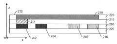
一実施形態において、デザインの第1の部分と第2の部分が相互排他的である空間は、ウェーハの上面に対して実質的に平行な平面にある。例えば、図2に示すように、ウェーハ基板200は、その上に形成されたいくつかの異なるパターニングしたフィーチャを有してもよい。図2および本明細書に記載されるその他の図面に示されるパターニングしたフィーチャは、任意の特定のウェーハ上の任意の特定のパターニングしたフィーチャを提示することを意図していない。代わりに、本明細書に記載された図に示されるパターニングしたフィーチャは、デザインの第1の部分と第2の部分の間の様々な空間的関係を説明し、それにより本明細書に記載される実施形態の理解を深めることのみを意図している。 In one embodiment, the space in which the first and second parts of the design are mutually exclusive is in a plane substantially parallel to the top surface of the wafer. For example, as shown in FIG. 2, the
図2の例において、パターニングしたフィーチャ202および204は、ウェーハ基板200上の層206内に形成されてもよい。加えて、パターニングしたフィーチャ208および210が、ウェーハ基板200の同じ層内に形成されてもよい。しかしながら、パターニングしたフィーチャ202および204はウェーハ上に実行される第1のプロセスステップで形成されるのに対し、パターニングしたフィーチャ208および210はウェーハ上に実行される第2のプロセスステップで形成される。したがって、パターニングしたフィーチャ202および204はウェーハデザインの第1の部分の一部と見做され得るのに対し、パターニングしたフィーチャ208および210はウェーハデザインの第2の部分の一部と見做され得る。 In the example of FIG. 2, the patterned features 202 and 204 may be formed in
図2にさらに示すように、パターニングしたフィーチャ202および204とパターニングしたフィーチャ208および210は、ウェーハの上面212に対して実質的に平行な平面内で相互排他的であることによって空間内で相互排他的である。言い換えると、パターニングしたフィーチャ202および204とパターニングしたフィーチャ208および210は、図2に示すxおよびy方向において重複しない位置取りを有するので、異なるパターニングしたフィーチャに対応するデザインの異なる部分は、ウェーハの上面に対して実質的に平行なx、y平面において相互排他的である。 As further shown in FIG. 2, the patterned features 202 and 204 and the patterned features 208 and 210 are mutually exclusive in space by being mutually exclusive in a plane substantially parallel to the
したがって、ウェーハの検査は、ウェーハ上にパターニングしたフィーチャ202および204を形成したプロセスステップと、ウェーハ上にパターニングしたフィーチャ208および210を形成したプロセスステップとの間には実行され得ない。代わりに、検査は、パターニングしたフィーチャ202および204とパターニングしたフィーチャ208および210がウェーハ上に形成された後にのみ実行され得る。加えて、検査は、図2に示され本明細書にさらに説明される別のパターニングしたフィーチャがウェーハ上に形成される前に、実行され得る。 Therefore, the inspection of the wafer cannot be performed between the process step of forming the
図3は、ウェーハ上に実行される異なるプロセスステップでウェーハ上に形成され、ウェーハの上面に対して実質的に平行な平面において相互排他的である、ウェーハデザインの異なる部分の別例を示す。例えば、ウェーハ300のデザインの第1の部分は、ウェーハに実行される第1のプロセスステップでウェーハ上に形成されたパターニングしたフィーチャ302、304、306および308を含んでもよい。ウェーハ300のデザインの第2の部分は、ウェーハ上に実行される第2のプロセスステップでウェーハ上に形成されたパターニングしたフィーチャ310、312、314および316を含んでもよい。加えて、ウェーハ300のデザインの第3の部分は、ウェーハ上に実行される第3のプロセスステップでウェーハ上に形成されたパターニングしたフィーチャ318、320、322および324を含んでもよい。したがって、図3に示すように、デザインの各部分に含まれるパターニングしたフィーチャは、図3に示されるxおよびy方向によって規定されるx、y平面において相互排他的である。言い換えると、図3に示されるパターニングしたフィーチャはいずれも、ウェーハの上面に対して平行なx、y平面において重複する位置を有することがない。そのため、図3に示されるデザインの異なる部分それぞれは、ウェーハの上面に対して実質的に平行な平面において相互排他的である。 FIG. 3 shows another example of different parts of a wafer design that are formed on a wafer in different process steps performed on the wafer and are mutually exclusive in a plane substantially parallel to the top surface of the wafer. For example, the first part of the design of the
別の実施形態において、デザインの第1の部分に含まれるパターニングしたフィーチャは、デザインの第2の部分に含まれるパターニングしたフィーチャと相互排他的である。言い換えると、デザインの第1の部分に含まれるパターニングしたフィーチャはいずれも、デザインの第2の部分に含まれることはない。そのため、いずれの1つのパターニングしたフィーチャも、デザインの1つの部分にのみ含まれ得る。加えて、1つのパターニングしたフィーチャの異なる部分は、デザインの異なる部分に含まれるとは見做され得ない。例えば、コンタクトの線形層と、同じコンタクトの異なる部分は、それらが異なるプロセスステップで形成されたとしてもデザインの異なる部分に含まれることはない。特に、本明細書にさらに説明されるように、デザインの異なる部分に対する欠陥の位置、ならびに、デザインの異なる部分と、ウェーハ上に実行される異なるプロセスステップとの相関が、異なる欠陥を異なるプロセスステップに関連付けるために用いられる。したがって、ウェーハ上の単一のパターニングしたフィーチャの異なる部分が、検査システムの出力において(それらが検査システムに対しては単一のパターニングしたフィーチャとして現れる場合)互いに弁別され得ない場合、デザインの異なる部分に対する欠陥の位置が十分な精度で判定され得ず、それにより、欠陥が、デザインの異なる部分に相関される異なるプロセスステップに十分な精度で関連付けられることを妨げる。 In another embodiment, the patterned features contained in the first part of the design are mutually exclusive with the patterned features contained in the second part of the design. In other words, none of the patterned features contained in the first part of the design are contained in the second part of the design. Therefore, any one patterned feature can be included in only one part of the design. In addition, different parts of one patterned feature cannot be considered to be included in different parts of the design. For example, a linear layer of contacts and different parts of the same contact are not included in different parts of the design, even if they are formed in different process steps. In particular, as further described herein, the location of defects relative to different parts of the design, as well as the correlation between different parts of the design and the different process steps performed on the wafer, will result in different process steps for different defects. Used to associate with. Therefore, if different parts of a single patterned feature on a wafer cannot be distinguished from each other at the output of the inspection system (if they appear as a single patterned feature to the inspection system), then the design will be different. The location of the defect with respect to the part cannot be determined with sufficient accuracy, thereby preventing the defect from being associated with different process steps correlated with different parts of the design with sufficient accuracy.
いくつかの実施形態において、デザインの第1の部分は、デザインの第2の部分の上側または下側に形成されない。例えば、図2に示すように、いくつかのパターニングしたフィーチャは、ウェーハ上にパターニングした別のフィーチャ(複数)の上側または下側のウェーハに形成されてもよい。特に、図2に示すように、層216のパターニングしたフィーチャ214は、層206上のパターニングしたフィーチャ202の上側に形成されてもよい。加えて、層220のパターニングしたフィーチャ218は、層206のパターニングしたフィーチャ202、204、208および210ならびに層216のパターニングしたフィーチャ214の上側に形成されてもよい。したがって、パターニングしたフィーチャ214は、パターニングしたフィーチャ202がデザインの別の部分の一部である場合にデザインの1つの部分の一部ではない。加えて、パターニングしたフィーチャ218は、パターニングしたフィーチャ202および204、パターニングしたフィーチャ208および210、またはパターニングしたフィーチャ212がデザインの別の部分の一部である場合にデザインの1つの部分の一部ではない。例えば、本明細書にさらに説明されるように、デザインの異なる部分に対する欠陥の位置、ならびに、デザインの異なる部分と、ウェーハ上に実行される異なるプロセスステップとの相関が、異なる欠陥を異なるプロセスステップに関連付けるために用いられる。したがって、デザインの異なる部分がウェーハに重複する場合(それらが互いに上側または下側に形成される場合のように)、デザインの異なる部分に対する欠陥の位置は十分な精度で判定され得ず、それにより、欠陥が、デザインの異なる部分に相関される異なるプロセスステップに十分な精度で関連付けられることを妨げる。 In some embodiments, the first portion of the design is not formed above or below the second portion of the design. For example, as shown in FIG. 2, some patterned features may be formed on the upper or lower wafer of another patterned feature on the wafer. In particular, as shown in FIG. 2, the
別の実施形態において、デザインの第1と第2の部分はウェーハの同じ層上に形成される。例えば、図2に示すように、ウェーハ上に第1のプロセスステップで形成されたデザインの第1の部分の一部であり得るパターニングしたフィーチャ202および204と、ウェーハ上に第2のプロセスステップで形成されたデザインの第2の部分の一部であり得るパターニングしたフィーチャ208および210は、ウェーハの同じ層上に形成されてもよい。別の例において、図3に示すように、ウェーハ上に第1のプロセスステップで形成されたデザインの第1の部分の一部であり得るパターニングしたフィーチャ302、304、306および308と、ウェーハ上に第2のプロセスステップで形成されたデザインの第2の部分の一部であり得るパターニングしたフィーチャ310、312、314および316と、ウェーハ上に第3のプロセスステップで形成されたデザインの第3の部分の一部であり得るパターニングしたフィーチャ318、320、322および324は、ウェーハの同じ層上に形成されてもよい。 In another embodiment, the first and second parts of the design are formed on the same layer of wafer. For example, as shown in FIG. 2, patterned
加えて、図2に示すように、同じ層上に形成されたデザインのパターニングしたフィーチャは、z方向における位置が同じであってもよい。しかしながら、同じ層上に形成されたデザインの異なる部分のパターニングしたフィーチャは、高さが同じでも同じでなくてもよい。加えて、同じ層上に形成されたデザインの異なる部分のパターニングしたフィーチャは、z方向に沿って異なる位置を有してもよく、その結果、デザインの異なる部分におけるパターニングしたフィーチャの最下面および/または最上面が、z方向に沿って同じx、y平面に配置されても配置されなくてもよいこととなる。しかしながら、好ましくは、デザインの異なる部分両方(または全て)におけるパターニングしたフィーチャの最上面は、それらが検査システムの出力で適切に検出され得ない程度よりもz方向に互いに離れて配置されることはない。言い換えると、デザインの異なる部分における異なるパターニングしたフィーチャは、それらが適切にイメージング(または検出)され得ない程に焦平面から離れることがない限り、検査システムの焦平面に対して異なる位置をとってもよい。したがって、検査対象の(あるいはレビュー対象の)全てのパターニングしたフィーチャの位置のz方向における差は、好ましくは、検査システム(あるいは欠陥レビューシステム)の焦点深度よりも小さい。 In addition, as shown in FIG. 2, the patterned features of the design formed on the same layer may have the same position in the z direction. However, the patterned features of different parts of the design formed on the same layer may or may not be the same height. In addition, the patterned features of different parts of the design formed on the same layer may have different positions along the z direction, resulting in the bottom surface and / or the bottom surface of the patterned features in the different parts of the design. Alternatively, the uppermost surface may or may not be arranged in the same x and y planes along the z direction. However, preferably, the top surfaces of the patterned features in both (or all) different parts of the design are placed farther apart in the z direction than they cannot be properly detected in the output of the inspection system. Absent. In other words, different patterned features in different parts of the design may take different positions with respect to the focal plane of the inspection system, as long as they are not too far from the focal plane to be properly imaged (or detected). .. Therefore, the difference in z-direction between the positions of all patterned features to be inspected (or reviewed) is preferably less than the depth of focus of the inspection system (or defect review system).
さらに別の実施形態において、デザインの第1と第2の部分はウェーハの異なる層上に形成され、検出器の出力はウェーハの上面より下側の欠陥の深さに応じても応じなくてもよい。例えば、デザインの異なる部分はウェーハの同じ層上に形成される必要はない。しかしながら、デザインの異なる部分は好ましくは、それらが検査システムの出力において、また任意選択的に欠陥レビューツールの出力で識別され得る方式でウェーハ上に形成される。例えば、デザインの異なる部分は、上記の検査システムの焦点深度内に依然としてありながらウェーハの異なる層上に配置されてもよい。加えて、デザインの1つ以上の部分は、デザインのその部分(それらの部分)より上側のウェーハ上に形成された1つ以上のパターンなしまたはパターン付き材料の下側に配置されてもよいが、それは、これらの重なる材料が検査システムあるいは欠陥レビューシステムの、デザインのその部分(それらの部分)におけるパターニングしたフィーチャを「見る」能力に干渉しない場合に限る。例えば、デザインの1つの部分は検査システムあるいは欠陥レビューシステムに対して透過性(実質的にまたは少なくとも部分的に透過性)である1つ以上の材料の下側に配置されてもよく、その結果それらの1つ以上の重なる材料が、デザインの部分からの光(またはその他のエネルギー、例えば電子)の検出を阻止しない。こうして、デザインの部分と、その中に配置された欠陥は、それらが検査システム(および、欠陥を、デザインの異なる部分に配置された欠陥の異なる部分に分離するために欠陥レビュー画像が用いられる場合は欠陥レビューシステムの可能性もある)に対して「見える」状態である限り、必ずしもウェーハの最上層にある必要はない。走査電子顕微鏡(SEM)として構成された欠陥レビューシステムによって生成された画像が、デザインの第1と第2の部分に対する欠陥の位置を判定するために用いられた場合、全ての欠陥は好ましくは、ウェーハの最上層に対するそれらの位置にかかわらずSEMに対して「見える」状態である。ウェーハ上で最上ではないが、それでもSEMに対して見える層の例は、多ステップによって生じた欠陥を観察するためにSEMレビューされ得るライン層の中間端部を含む。 In yet another embodiment, the first and second parts of the design are formed on different layers of the wafer and the output of the detector may or may not depend on the depth of defects below the top surface of the wafer. Good. For example, different parts of the design need not be formed on the same layer of wafer. However, the different parts of the design are preferably formed on the wafer in such a way that they can be identified at the output of the inspection system and optionally at the output of the defect review tool. For example, different parts of the design may be placed on different layers of the wafer while still within the depth of focus of the inspection system described above. In addition, one or more parts of the design may be located below one or more unpatterned or patterned materials formed on the wafer above that part of the design (these parts). Only if these overlapping materials do not interfere with the ability of the inspection system or defect review system to "see" the patterned features in that part of the design (these parts). For example, one part of the design may be placed underneath one or more materials that are permeable (substantially or at least partially permeable) to the inspection system or defect review system, as a result. One or more of those overlapping materials do not block the detection of light (or other energy, eg electrons) from parts of the design. Thus, the parts of the design and the defects placed therein are inspected system (and when defect review images are used to separate the defects into different parts of the defects placed in different parts of the design. Does not necessarily have to be on top of the wafer, as long as it is "visible" to (possibly a defect review system). When images generated by a defect review system configured as a scanning electron microscope (SEM) are used to determine the location of defects with respect to the first and second parts of the design, all defects are preferably. It is "visible" to the SEM regardless of their position with respect to the top layer of the wafer. Examples of layers that are not top on the wafer but are still visible to the SEM include the mid-end of the line layer that can be SEM reviewed to observe defects caused by multiple steps.
加えて、本明細書にさらに説明されるように、検査システム(あるいは欠陥レビューシステム)の出力が、ウェーハの上面(または単に、z次元に対する、パターニングしたフィーチャの異なる位置)より下側のウェーハ上に形成されたパターニングしたフィーチャの深さに応じていても応じていなくても、その情報は、欠陥が位置しているデザインの異なる部分を判定するために、本明細書に記載される実施形態によって、または本明細書に記載される実施形態では用いられない。言い換えると、欠陥は、それらのz方向における位置に基づいては、デザインの異なる部分に相関されない。 In addition, as further described herein, the output of the inspection system (or defect review system) is on the wafer below the top surface of the wafer (or simply at different positions of the patterned features with respect to the z dimension). The information, whether or not it depends on the depth of the patterned features formed in, is described herein to determine different parts of the design where defects are located. Not used by or in the embodiments described herein. In other words, defects are not correlated with different parts of the design based on their position in the z direction.
さらに図5に示すように、ウェーハは、ウェーハを処理するプロセスツールA、500に配置されてもよい。プロセスツールAによってウェーハに実行されるプロセスステップは、第1の多ステッププロセスであり得る。次にウェーハは、ウェーハを処理するプロセスツールB、502に配置されてもよい。プロセスツールBによってウェーハに実行されるプロセスステップは、同じ多ステッププロセスのうち第2のプロセスであり得る。このように、第1のプロセスステップと第2のプロセスステップは、ウェーハ上の同じデバイスの少なくとも一部分を形成するために相前後して実行される連続したプロセスステップであってよい。ウェーハは任意選択的に、プロセスツールC、504または、第1の2つのプロセスステップにリンクされるウェーハ上の連続したプロセスステップ(すなわち、第1の2つのプロセスステップと同じ多ステップの一環である)を実行する任意の他のプロセスツールに配置されてもよい。 Further, as shown in FIG. 5, the wafer may be arranged in the process tool A, 500 for processing the wafer. The process step performed on the wafer by process tool A can be the first multi-step process. The wafer may then be placed in process tool B, 502, which processes the wafer. The process step performed on the wafer by process tool B can be the second process of the same multi-step process. Thus, the first process step and the second process step may be successive process steps that are performed back and forth to form at least a portion of the same device on the wafer. The wafer is optionally part of process tool C, 504, or the same multi-step process steps on the wafer that are linked to the first two process steps (ie, the same multi-step process as the first two process steps). ) May be placed in any other process tool that executes.
第1と第2のプロセスステップは、いくつかの異なる多ステッププロセスのいずれであってもよい。一実施形態において、第1のプロセスステップは多数のパターニングステッププロセスの第1のパターニングステップを含み、第2のプロセスステップは多数のパターニングステッププロセスの第2のパターニングステップを含む。例えば、多数のパターニングプロセスは、ウェーハ上にパターンを形成するための一続きのリソグラフィーとエッチングステップ(例えば、第1のリソグラフィー、第1のエッチングに続く第2のリソグラフィー、第2のエッチング等)を包含してもよい。こうして、第1のプロセスステップは二段階ダブルパターニング法の第1のエッチングステップであってよく、第2のプロセスステップは二段階ダブルパターニング法の第2のエッチングステップであってよい。加えて、プロセスステップは2つのプロセスステップに限定されず、任意の多数のステップに拡張されてもよい(例えばダブルパターニング、カッドパターニング等)。多数のステッププロセスにおける最終プロセスステップの後で、ウェーハは、プロセス事項を特定し、欠陥位置を表すウェーハマップ等の検査結果を出力するように構成された検査ツール506(またはその他の光学機器)に移される。そこで、完全ウェーハ検査508が検査ツールによって実行され得る。 The first and second process steps may be any of several different multi-step processes. In one embodiment, the first process step comprises a first patterning step of a number of patterning step processes and the second process step comprises a second patterning step of a number of patterning step processes. For example, many patterning processes involve a series of lithography and etching steps to form a pattern on a wafer (eg, first lithography, second lithography following first etching, second etching, etc.). It may be included. Thus, the first process step may be the first etching step of the two-step double patterning method, and the second process step may be the second etching step of the two-step double patterning method. In addition, the process steps are not limited to the two process steps and may be extended to any number of steps (eg, double patterning, quad patterning, etc.). After the final process step in a number of step processes, the wafer is placed on an inspection tool 506 (or other optical instrument) configured to identify process items and output inspection results such as wafer maps representing defect locations. Be transferred. There, a complete wafer inspection 508 can be performed by the inspection tool.
別の実施形態において、デザインの第1の部分は、N型金属酸化物半導体(NMOS)トランジスタの構造を含み、デザインの第2の部分はP型金属酸化物半導体(PMOS)トランジスタの構造を含む。例えば、本明細書に記載される実施形態は、エッチングと成膜ステップを反復する多プロセスステップを監視するために本明細書に記載される検査プロセスが用いられ得るNMOSプロセスステップとPMOSプロセスステップに用いられてもよい。いくつかの実施形態において、NMOSトランジスタおよびPMOSトランジスタの構造はウェルである。こうして、本明細書に記載される実施形態は、NウェルおよびPウェルの定義を監視するために用いられ得る。NMOSおよびPMOSトランジスタの構造は、拡張インプラントおよび金属パターニング層等の他の構造を含んでもよい。ウェルまたはNMOSおよびPMOSトランジスタの任意の他の構造は、当技術分野で知られる任意の適切な方式で形成されて任意の適切な構成を有してもよい。 In another embodiment, the first part of the design comprises the structure of an N-type metal oxide semiconductor (NMOS) transistor and the second part of the design comprises the structure of a P-type metal oxide semiconductor (SiO) transistor. .. For example, the embodiments described herein include the NMOS process steps and the MIMO process steps in which the inspection processes described herein can be used to monitor multi-process steps that iterate over etching and film formation steps. It may be used. In some embodiments, the structure of the NMOS transistor and the polyclonal transistor is a well. Thus, the embodiments described herein can be used to monitor the definitions of N-wells and P-wells. The structure of the NMOS and ProLiant transistors may include other structures such as expansion implants and metal patterning layers. The wells or any other structure of the NMOS and ProLiant transistors may be formed in any suitable manner known in the art and have any suitable configuration.
別の実施形態において、第1と第2のプロセスステップは、配線形成プロセス(back end of line、BEOL)メタライゼーションプロセスの一環である。メタライゼーションプロセスは、ウェーハ上に任意の金属層(複数)(例えば、金属層1(M1)、金属層2(M2)等)を形成するために用いられる、当技術分野で知られる任意の適切なメタライゼーションプロセスを含んでもよい。 In another embodiment, the first and second process steps are part of a back end of line (BEOL) metallization process. The metallization process is used to form any metal layer (s) on the wafer (eg, metal layer 1 (M1), metal layer 2 (M2), etc.), any suitable known in the art. Metallization process may be included.
第1と第2のプロセスステップは、同じ検査プロセス(あるいは同じ欠陥レビュープロセス)において検査システム(あるいは欠陥レビューシステム)に対して見える状態である、ウェーハ上のデザインの異なる(相互排他的な)部分を形成するために組み合わせて用いられる任意の他のプロセスステップをも含んでもよい。例えば、第1と第2のプロセスステップは、ハードマスク成膜およびパターニング(シリコンゲルマニウム(SiGe)およびシリコンカーバイド(SiC)ステップ向け)、(SiGeへの)アルミシリサイドインプラントのためのプロセスステップを含んでもよい。 The first and second process steps are different (mutually exclusive) parts of the design on the wafer that are visible to the inspection system (or defect review system) in the same inspection process (or the same defect review process). It may also include any other process step used in combination to form. For example, the first and second process steps may include process steps for hardmask deposition and patterning (for Silicon Germanium (SiGe) and Silicon Carbide (SiC) steps), aluminum silicide implants (to SiGe). Good.
コンピュータサブシステム(複数)は、ウェーハ上の欠陥をその出力に基づいて検出するように構成される。こうして、ウェーハは欠陥に関して検査され得る。ウェーハ上の欠陥をその出力に基づいて検出することは、当技術分野で知られる任意の適切な方式で実行され得る。例えば、出力は、1つ以上の欠陥検出アルゴリズムおよび/または方法への入力として用いられてもよい。そのような欠陥検出アルゴリズムの一例は、出力を閾値と比較するように構成されてもよく、閾値を超えた1つ以上の値を有する出力はいずれも潜在的欠陥として識別され得るのに対し、閾値を超えた1つ以上の値を有していない出力はいずれも潜在的欠陥として識別され得ない。しかしながら、本明細書に記載される実施形態はいずれの特定の欠陥検出方法および/またはアルゴリズムにも限定されず、適切な欠陥検出方法および/またはアルゴリズムは、検査システムの構成、ウェーハのタイプ、ウェーハ上で検出されるべき対象の欠陥(複数)(DOI(複数))のタイプ等のいくつかの因子に依存して変わり得る。 Computer subsystems are configured to detect defects on the wafer based on their power output. In this way, the wafer can be inspected for defects. Detecting defects on a wafer based on its power output can be performed by any suitable method known in the art. For example, the output may be used as an input to one or more defect detection algorithms and / or methods. An example of such a defect detection algorithm may be configured to compare the output to a threshold, whereas any output having one or more values above the threshold can be identified as a potential defect. Any output that does not have one or more values above the threshold cannot be identified as a potential defect. However, the embodiments described herein are not limited to any particular defect detection method and / or algorithm, and the appropriate defect detection method and / or algorithm may be the configuration of the inspection system, the type of wafer, the wafer. It can vary depending on several factors, such as the type of defect (DOI) of interest to be detected above.
いくつかの実施形態において、欠陥を検出することは、デザインの第1のおよび/または第2の部分に基づいて実行されてもよい。例えば、欠陥を検出するために用いられる欠陥検出アルゴリズムおよび/または方法の1つ以上のパラメータは、出力が生成したウェーハの位置と、その位置に対応するデザインの部分に依存して変わり得る。このように、欠陥を検出することは、デザイン主導の半導体ウェーハ欠陥検査または計測を含んでもよい。デザイン主導の半導体ウェーハ欠陥検査または計測の方法およびシステムの例は、あたかも本明細書に完全に記載されているかのように参考として援用される、2005年4月26日にBevisに発行された米国特許第6,886,153号明細書に記載されている。本明細書に記載される実施形態は、さらにこの特許に記載されるように構成されてもよい。 In some embodiments, detecting defects may be performed based on the first and / or second part of the design. For example, one or more parameters of the defect detection algorithm and / or method used to detect defects may vary depending on the position of the wafer from which the output was generated and the part of the design corresponding to that position. Thus, defect detection may include design-driven semiconductor wafer defect inspection or measurement. Examples of design-driven semiconductor wafer defect inspection or measurement methods and systems are incorporated by reference in the United States, published April 26, 2005, as if they were fully described herein. It is described in Pat. No. 6,886,153. The embodiments described herein may be configured as further described in this patent.
ウェーハ上の欠陥の検出の結果は、任意の適切なフォーマットで出力されてもよい。例えば、ウェーハ上の欠陥を検出した結果は、検査結果を含み、本明細書に記載されるその他の機能を実行するためにコンピュータサブシステム(複数)によって用いられ得るファイルで出力されてもよい。加えて、欠陥検出の結果は、図4に示すウェーハマップ416とパレート図418等のいくつかの異なる結果を生成するために用いられてもよい。ウェーハマップ416はプロセスB後にウェーハ上で検出された欠陥の位置を示し得るのに対し、パレート図418はプロセスB後にウェーハ上で検出されたいくつかの異なるタイプの欠陥または事象を示し得る。したがって本例では、ウェーハマップにその位置が示されパレート図にそのタイプが示される欠陥は、プロセスステップAとプロセスステップB両方による欠陥を含んでもよい。したがって、本明細書にさらに説明されるように、コンピュータサブシステム(複数)は、検出された欠陥を、プロセスステップAによる欠陥と、プロセスステップBによる欠陥に分割するためのいくつかの機能を実行するように構成されてもよい。 The result of defect detection on the wafer may be output in any suitable format. For example, the results of detecting defects on the wafer may be output in a file that includes inspection results and can be used by computer subsystems to perform other functions described herein. In addition, the defect detection results may be used to generate several different results, such as the
コンピュータサブシステム(複数)は、デザインの第1と第2の部分に対する欠陥の位置を判定するようにも構成される。例えば、図4に示すように、ウェーハ上にプロセスステップAとプロセスステップBの両方が実行された後で、デザインAのパターニングしたフィーチャとデザインBのパターニングしたフィーチャがウェーハ406上に形成される。加えて、図4に示すように、欠陥420はデザインAのパターニングしたフィーチャ404のうち1つの中にまたはその上に形成され得るのに対し、欠陥422はデザインBのパターニングしたフィーチャ412のうち1つの中にまたはその上に形成され得る。パターニングしたフィーチャ404および412それぞれのうち一方の中または一方の上に1つの欠陥が配置されるが、任意の個数の欠陥が、異なるプロセスステップに対応するデザインの部分に含まれるパターニングしたフィーチャの中またはその上に配置されてもよいことを理解すべきである。加えて、図4に示される欠陥420および422の形状、サイズおよび位置は、任意のウェーハ上で検出される任意の実際の欠陥の任意の実際の特徴を示すことを意図していない。本明細書に記載される実施形態は、したがって、ウェーハ上に形成されたフィーチャに対する欠陥の位置を判定するように構成されてもよく、次に、どのフィーチャがデザインのどの部分に含まれるかに関する情報を用いて、欠陥がその上またはその中に位置しているデザインの部分を判定する。図4に示される例において、判定ステップは、欠陥420の位置がフィーチャ404のうち1つ上にまたはその中に位置していること、また、フィーチャ404が、デザインAとして指定されるデザインの部分に含まれることを判定することを含んでもよい。加えて、判定ステップは、欠陥422の位置がフィーチャ412のうち1つ上にまたはその中に位置していること、また、フィーチャ412が、デザインBとして指定されるデザインの部分に含まれることを判定することを含んでもよい。したがって、判定ステップは、デザインAとして指定されるデザインの部分に対する欠陥420の位置と、デザインBとして指定されるデザインの部分に対する欠陥422の位置を判定することを含んでもよい。 Computer subsystems are also configured to determine the location of defects with respect to the first and second parts of the design. For example, as shown in FIG. 4, after both process step A and process step B have been performed on the wafer, the patterned features of design A and the patterned features of design B are formed on the
一実施形態において、上記のように欠陥の位置を判定することは、検出器によって生成された欠陥に対する出力を、デザインの第1の部分または第2の部分に整列させることを含む。例えば、図4に示すように、コンピュータサブシステム(複数)は、ステップ424に示すように欠陥が整列をデザインするように構成されてもよい。別の例において、図5に示すように、コンピュータサブシステム(複数)は、相関510をデザインするために光学を実行するように構成される。このステップにおいて、コンピュータサブシステム(複数)は、両方のプロセスステップからのデザインファイルを、検出された欠陥位置とオーバーレイしてもよい。そのようなオーバーレイは、あたかも本明細書に完全に記載されているかのように参考として援用される、2009年8月4日にZafarらに発行された米国特許第7,570,796号明細書に記載されている。本明細書に記載される実施形態は、この特許に記載される任意のステップ(複数)を実行するように構成されてもよく、またさらに、この特許に記載されるように構成されてもよい。 In one embodiment, determining the location of a defect as described above involves aligning the output for the defect generated by the detector with a first or second part of the design. For example, as shown in FIG. 4, the computer subsystem may be configured such that the defects design the alignment as shown in
こうして、検出器の出力は、出力のパターンに適合(または実質的に適合)する、デザインの異なる部分内のパターンを識別するために、デザインの異なる部分に整列されてもよい。デザインの異なる部分における適合するパターンに関する情報は、次に、欠陥のデザイン空間座標、デザインのどの部分に欠陥が位置しているか、欠陥が位置しているデザインの部分に対する欠陥の位置等の、欠陥に関する情報を判定するために用いられ得る。 Thus, the output of the detector may be aligned to different parts of the design to identify patterns within different parts of the design that match (or substantially match) the pattern of the output. Information about matching patterns in different parts of the design can then be found in the design spatial coordinates of the defect, where in the design the defect is located, the location of the defect relative to the part of the design where the defect is located, etc. Can be used to determine information about.
別の実施形態において、デザインの第1と第2の部分はウェーハ上の異なる層上に形成され、検出器の出力が、ウェーハの上面の下側の欠陥の深さに応答する場合、デザインの第1と第2の部分に対する欠陥の位置を判定することは、ウェーハの上面の下側の欠陥の深さに基づいては実行されない。例えば、上記に詳細に規定したように、検出器の出力は、ウェーハの上面の下側の欠陥の深さに応答してもよい。しかしながら、そのような場合、ウェーハ上面の下側の欠陥の深さは、それ自体では、ウェーハ上に実行される異なるプロセスステップに起因する欠陥を分離するために用いられない。代わりに、本明細書にさらに説明されるように、デザインの異なる部分に対する欠陥の位置を判定するために好ましくは用いられるのは、デザインの部分自体である。 In another embodiment, if the first and second parts of the design are formed on different layers on the wafer and the output of the detector responds to the depth of defects underneath the top surface of the wafer, then the design. Determining the location of defects relative to the first and second portions is not performed based on the depth of the defects below the top surface of the wafer. For example, as detailed above, the output of the detector may respond to the depth of defects underneath the top surface of the wafer. However, in such cases, the depth of defects below the top surface of the wafer is not used by itself to separate defects due to different process steps performed on the wafer. Instead, as further described herein, it is the part of the design itself that is preferably used to determine the location of defects relative to different parts of the design.
別の実施形態において、1つ以上のコンピュータサブシステムは、検出された欠陥の部分をサンプリングするように構成され、欠陥の位置を判定することは、欠陥レビューサブシステムによって生成された、検出された欠陥のサンプリングされた部分の画像を、デザインの第1の部分または第2の部分に整列させることを含む。こうして、ウェーハが欠陥に関して検査された後で、欠陥はサンプリングされレビューされ得る。そのような1つの実施形態において、検出された欠陥の部分をサンプリングすることは、ウェーハにわたる欠陥の空間分布に基づいて判定された欠陥の異なる部分母集団から欠陥をランダムに選択することを含む。例えば、コンピュータサブシステム(複数)は、図5のステップ512に示すように、欠陥分布を理解するために、減じた数の欠陥をランダムにサンプリングすることにより欠陥をサンプリングするように構成されてもよい。次にウェーハはイメージングのために、欠陥レビューツール(例えば、KLA−Tencorから商業的に入手可能なeDR欠陥レビューツールまたは同等のSEM欠陥レビューツール)の欠陥レビューサブシステム等の欠陥レビューサブシステムに移送されてもよい。そこでコンピュータサブシステム(複数)は、図5のステップ514に示すように欠陥をレビューするように構成されてもよい。サンプリングされた欠陥は、あたかも本明細書に完全に記載されているかのように参考として援用される、2006年9月12日にObaraらに発行された米国特許第7,105,815号明細書に記載されるようにレビューされて分類されてもよい。本明細書に記載される実施形態は、この特許に記載される任意のステップ(複数)を実行するように構成されてもよく、またさらにこの特許に記載されるように構成されてもよい。図5に示すように、コンピュータサブシステム(複数)は、ステップ516に示すように、相関をデザインするために欠陥レビューを実行するように構成されてもよい。欠陥レビュー画像をデザインに相関することは、分析または歩留まり管理ツールに実行されてもよい。分析は、各サンプリングされてレビューされた欠陥をデザインと相関することを含み、それは、相関をデザインするための光学系に関して上記に詳しく説明したように実行されてもよい。こうして、デザインは、相関をレビューするためにデザインのレビュー画像にオーバーレイされてもよい。 In another embodiment, one or more computer subsystems are configured to sample a portion of the detected defect, and determining the location of the defect was generated by the defect review subsystem and was detected. Includes aligning an image of a sampled portion of a defect with a first or second portion of the design. Thus, after the wafer has been inspected for defects, the defects can be sampled and reviewed. In one such embodiment, sampling a portion of the detected defect comprises randomly selecting defects from a different partial population of the determined defects based on the spatial distribution of the defects across the wafer. For example, a computer subsystem may be configured to sample defects by randomly sampling a reduced number of defects in order to understand the defect distribution, as shown in step 512 of FIG. Good. The wafer is then transferred for imaging to a defect review subsystem such as a defect review subsystem of a defect review tool (eg, an eDR defect review tool commercially available from KLA-Tencor or an equivalent SEM defect review tool). May be done. The computer subsystem may then be configured to review defects as shown in
別の実施形態において、第1のプロセスステップはデザインの第1の部分のみに関する情報を用いて実行され、第2のプロセスステップはデザインの第2の部分のみに関する情報を用いて実行され、欠陥の位置を判定することはデザインの第1と第2の部分両方に関する情報を用いて実行される。例えば、図4に示すように、整列をデザインする欠陥は、デザインAとして指定されたデザインの部分内にどの欠陥が位置しているかを判定するために、プロセスAのデザインAへの相関426を用いてもよく、また、デザインBとして指定されたデザインの部分内にどの欠陥が位置しているかを判定するために、プロセスBのデザインBへの相関428を用いてもよい。したがって、各プロセスステップは、ウェーハ上に形成されるデザインの部分のみに関する情報を用いてもよいが、検査ステップは、検査(あるいはレビュー)によって考慮されるプロセスステップすべてにおいて形成されるデザインの全ての部分に関する情報を用いてもよい。 In another embodiment, the first process step is performed with information about only the first part of the design and the second process step is performed with information about only the second part of the design, which is defective. Determining the position is performed using information about both the first and second parts of the design. For example, as shown in FIG. 4, a defect designing an alignment has a
コンピュータサブシステム(複数)はさらに、欠陥の異なる部分を、デザインの第1と第2の部分に対する欠陥の位置に基づいて第1のプロセスステップまたは第2のプロセスステップに関連付けるように構成される。こうして、現在用いられている方法およびシステムは、2つの連続したプロセスステップ(例えばエッチングNo.1およびエッチングNo.2)を行い、次に単一の検査ステップを行って欠陥を第1と第2のプロセスステップに戻って相関することにより顕著に改良され得る。欠陥を異なるプロセスステップに戻って相関することは、本明細書にさらに説明されるように、欠陥を、異なるプロセスステップに対応するデザインの異なる部分に相関することによって可能にされる。例えば、光学サブシステムの出力および/または欠陥レビューによって生成した画像がデザイン情報に整列した後で、出力および/または画像にうまく整列したデザインの部分を形成したプロセスステップは、デザインの異なる部分と異なるプロセスステップとの間の呼応に基づいて判定され得る。本明細書に記載される実施形態によってもたらされる結果は、したがって、単一の欠陥母集団から生成された多数の欠陥部分母集団を含んでもよく、部分母集団それぞれは、ウェーハ上に実行される多プロセスステップのうち1つのみに関連付けられてもよい。 Computer subsystems are further configured to associate different parts of a defect with a first or second process step based on the location of the defect relative to the first and second parts of the design. Thus, the methods and systems currently in use perform two consecutive process steps (eg, Etching No. 1 and Etching No. 2), followed by a single inspection step to remove defects first and second. It can be significantly improved by going back to the process steps of and correlating. Correlating defects back to different process steps is made possible by correlating defects with different parts of the design that correspond to different process steps, as further described herein. For example, after the image generated by the output and / or defect review of the optical subsystem is aligned with the design information, the process steps that form the part of the design that is well aligned with the output and / or the image are different from the different parts of the design. It can be determined based on the correspondence between the process steps. The results provided by the embodiments described herein may therefore include a large number of defective subpopulations generated from a single defective population, each of which is performed on a wafer. It may be associated with only one of the multi-process steps.
検査システム出力(またはレビュー画像)およびデザイン情報は、各欠陥または各レビューされたイメージへのタグ等の印を、対応するプロセスステップに割り当てるために用いられ得る。例えば、図5のステップ518に示すように、コンピュータサブシステム(複数)は、各欠陥に関する個別のタグをプロセスツールに対して生成するように構成されてもよい。各欠陥をその対応するプロセスステップにタグ付けする(すなわち、各欠陥にタグまたはその他の印を割り当て、それは、欠陥が位置しているデザインの部分を形成したプロセスステップを示す)ことは、システムが、デザインの異なる部分に相関する欠陥の画像を生成するために欠陥レビューサブシステムを含み、欠陥レビューサブシステムを用いる実施形態において、欠陥レビューツールの1つ以上のコンピュータサブシステム(複数)によって実行され得る。図5のステップ520にさらに示すように、コンピュータサブシステム(複数)は、レビューされた欠陥とプロセスツールタグを、製造データベースまたは本明細書に記載される他の適切なコンピュータ可読記憶媒体等のデータベースに送信するように構成されてもよい。 The inspection system output (or review image) and design information can be used to assign a mark, such as a tag, to each defect or each reviewed image to the corresponding process step. For example, as shown in step 518 of FIG. 5, the computer subsystem may be configured to generate a separate tag for each defect for the process tool. Tagging each defect with its corresponding process step (ie, assigning a tag or other mark to each defect, which indicates the process step that formed the part of the design in which the defect is located) In an embodiment that includes a defect review subsystem to generate images of defects that correlate to different parts of the design and uses the defect review subsystem, it is performed by one or more computer subsystems of the defect review tool. obtain. As further shown in step 520 of FIG. 5, the computer subsystem displays the reviewed defects and process tool tags in a database such as a manufacturing database or other suitable computer-readable storage medium described herein. It may be configured to send to.
こうして、本明細書に記載される実施形態は、上記のBevisへの特許に記載されたような検査に基づいたデザインのもとに構築された。現在用いられる方法において、検査はデザイン主導である。本明細書に記載される実施形態はこの技法に基づいて構築され、任意選択的にデザインベースのSEMレビューからの情報を追加してもよい。実施形態はデザインおよび検査および/またはSEMレビューからの情報を得て、プロセスツール相関に基づいて分析を細分化する。 Thus, the embodiments described herein have been constructed under an inspection-based design as described in the above patent to Bevis. In the methods currently used, inspection is design driven. The embodiments described herein are constructed on the basis of this technique and optionally add information from a design-based SEM review. The embodiment takes information from design and inspection and / or SEM reviews and subdivides the analysis based on process tool correlation.
一実施形態において、コンピュータサブシステム(複数)は、第1と第2のプロセスステップのうち1つに関連する欠陥の異なる部分のうち1つの、1つ以上の特徴を判定するように構成される。例えば、第1のプロセスステップと関連する欠陥の第1の部分に関して、コンピュータサブシステム(複数)は、欠陥の第1の部分の1つ以上の特徴を判定するために、検査システムおよび/または欠陥レビューシステムによって生成された第1の部分の欠陥に関する情報を用いてもよい。そのような特徴(複数)は、例えば、ウェーハにわたる欠陥分布、第1の部分における欠陥の分類、欠陥分類毎の第1の部分内の欠陥の個数、第1の部分内の欠陥の個数対パターニングした構造のタイプ、または当技術分野で知られる任意の別の適切な特徴を含んでもよい。同じ特徴が、別のプロセスステップに対応する欠陥の別の部分に関して判定されることがある。言い換えると、異なるプロセスステップに対応する欠陥の各部分は、それぞれの他の部分から別個に、その独自の欠陥母集団として考慮されてもよく、当技術分野で知られる任意の欠陥母集団の特徴は、当技術分野で知られる任意の適切な方式で判定され得る。 In one embodiment, the computer subsystem is configured to determine one or more features of one of the different parts of the defect associated with one of the first and second process steps. .. For example, with respect to a first part of a defect associated with a first process step, a computer subsystem (s) is an inspection system and / or a defect to determine one or more features of the first part of the defect. Information about defects in the first part generated by the review system may be used. Such features include, for example, defect distribution across wafers, defect classification in the first portion, number of defects in the first portion for each defect classification, number of defects in the first portion vs. patterning. It may include the type of structure, or any other suitable feature known in the art. The same characteristics may be determined for different parts of the defect that correspond to different process steps. In other words, each part of the defect that corresponds to a different process step may be considered as its own defect population, separate from each other part, and is a feature of any defect population known in the art. Can be determined by any suitable method known in the art.
別の実施形態において、コンピュータサブシステム(複数)は、第1と第2のプロセスステップにそれぞれ関連付けられる欠陥の異なる部分に基づいて、第1と第2のプロセスステップそれぞれに関する第1と第2の検査結果を生成するように構成される。例えば、欠陥の異なる部分が異なるプロセスステップに関連付けられて欠陥が(任意選択的に)分類されると、各プロセスステップに関する正規化された欠陥分布を特定するパレート図等の、欠陥の異なる部分に関する情報が生成され得る。そのような例のうち一例において、各欠陥をその対応するプロセスステップにタグ付けした結果が、各プロセスステップまたは各プロセスツールに関する別個のパレートを生成するために用いられ得る。別のそのような例において、ダブルパターニングプロセスに関して、コンピュータサブシステム(複数)は2つのパレートを生成してもよく、一方は第1のリソグラフィー−エッチングシーケンスであり、他方は第2のリソグラフィー−エッチングシーケンスである。こうして、図5のステップ522に示すようにコンピュータサブシステム(複数)はプロセスツール毎の結果を生成するように構成されてもよい。例えば、図4に示すように、コンピュータサブシステム(複数)は、プロセスAに関するウェーハマップ430およびプロセスAに関するパレート図432を生成し、プロセスBに関するウェーハマップ434およびプロセスBに関するパレート図436を生成するように構成されてもよい。したがって、各プロセスステップに関して、別々で別個の検査結果が生成されてもよい。別々で別個の検査結果は、異なる検査結果ファイルに含まれても、同じ検査結果ファイルに含まれてもよい。 In another embodiment, the computer subsystem (s) is a first and second process step for each of the first and second process steps, based on different parts of the defects associated with the first and second process steps, respectively. It is configured to generate test results. For example, when different parts of a defect are associated with different process steps and the defects are classified (optionally), then for different parts of the defect, such as a Pareto chart that identifies a normalized defect distribution for each process step. Information can be generated. In one such example, the result of tagging each defect with its corresponding process step can be used to generate a separate pare for each process step or each process tool. In another such example, for a double patterning process, the computer subsystem may generate two pallets, one in the first lithography-etching sequence and the other in the second lithography-etching. It is a sequence. Thus, as shown in step 522 of FIG. 5, the computer subsystem may be configured to generate results for each process tool. For example, as shown in FIG. 4, the computer subsystem produces a
付加的な実施形態において、1つ以上のコンピュータサブシステムは、第1と第2のプロセスステップを、第1と第2のプロセスステップそれぞれに関連付けられた欠陥の異なる部分に基づいて別個に監視するように構成される。言い換えると、第1のプロセスステップに関連付けられた欠陥の1つの部分が、第1のプロセスステップを監視するために用いられることができ、第2のプロセスステップに関連付けられた欠陥の別の部分が、第2のプロセスステップを監視するために用いられることができる、等である。本明細書に記載されるシステムは、したがって、単一の検査ステップを用いて多プロセスステップを監視するように構成されてもよい。加えて、欠陥画像は、あたかも本明細書に完全に記載されているかのように参考として援用される、1998年6月2日にLaらに発行された、欠陥管理および追尾に関する米国特許第5,761,064号明細書に記載されるように分析されて分類されてもよい。本明細書に記載される実施形態は、この特許に記載される任意のステップ(複数)を実行するように構成されてもよく、またさらにこの特許に記載されるように構成されてもよい。プロセス監視は、当技術分野で知られる任意の別の適切なプロセス監視をも含んでもよい。加えて、本明細書にさらに説明されるように、プロセスタグに基づいて、異なるプロセスステップに関して一意的な欠陥分布と正規化された欠陥チャートが生成されてもよく、それは、各プロセスツールにおける欠陥を理解するにあたり補助となり得る。 In an additional embodiment, one or more computer subsystems monitor the first and second process steps separately based on different parts of the defects associated with each of the first and second process steps. It is configured as follows. In other words, one part of the defect associated with the first process step can be used to monitor the first process step and another part of the defect associated with the second process step. , Can be used to monitor a second process step, etc. The system described herein may therefore be configured to monitor multiple process steps using a single inspection step. In addition, defect images are incorporated by reference as if they were fully described herein, US Pat. No. 5, Issued to La et al., June 2, 1998, for defect management and tracking. , 761,064 may be analyzed and classified as described in the specification. The embodiments described herein may be configured to perform any of the steps described in this patent, or may be further configured as described in this patent. Process monitoring may also include any other suitable process monitoring known in the art. In addition, as further described herein, process tags may generate unique defect distributions and normalized defect charts for different process steps, which are defects in each process tool. Can help in understanding.
したがって、本明細書に記載される実施形態は、別のシステムおよび方法よりも有利ないくつかの点を提供する。例えば、欠陥管理および検査およびデザインデータを組み合わせる従来のシステムおよび方法は、単一のプロセスステップを単一の検査ステップで監視することができる。対照的に、本明細書に記載される実施形態は、単一の検査/レビュープロセスの出力を、多プロセスステップに戻して相関して、単一の検査プロセスを用いて多プロセスステップを監視するためのシステムを提供する。したがって、本明細書に記載される実施形態は、連続した製造プロセスステップのために、検査ステップの低減を可能にする。そのため、本明細書に記載される実施形態は検査プロセスに必要な時間量を低減できる。特に、本明細書にさらに説明されるように、実施形態は、連続した製造プロセスステップの最終ステップの後にのみ実行される検査を用いる。単一の検査ステップは、多プロセスステップ(検査前の最終プロセスステップに先立って実行されるステップを含めて)のための情報を抽出し、単一のステップを用いて多プロセスステップを監視するために、欠陥レビューおよびデザイン情報と合わせて用いられ得る。 Therefore, the embodiments described herein provide some advantages over other systems and methods. For example, traditional systems and methods that combine defect management and inspection and design data can monitor a single process step in a single inspection step. In contrast, the embodiments described herein correlate the output of a single inspection / review process back into a multi-process step and monitor the multi-process step using a single inspection process. Provides a system for. Therefore, the embodiments described herein allow for a reduction in inspection steps due to the continuous manufacturing process steps. Therefore, the embodiments described herein can reduce the amount of time required for the inspection process. In particular, as further described herein, embodiments use inspections that are performed only after the final step of a series of manufacturing process steps. A single inspection step extracts information for a multi-process step (including steps performed prior to the final pre-inspection process step) and uses a single step to monitor the multi-process step. Can be used in conjunction with defect reviews and design information.
加えて、現在用いられている方法およびシステムのいくつかは、1つのプロセスツールと単一のプロセスステップを監視するために、デザイン、欠陥レビューおよび検査結果を用いる。対照的に、本明細書に記載される実施形態は、多プロセスステップを監視するために、デザインおよび検査情報(また任意選択的に欠陥レビュー情報)および各プロセスステップへの相関を用いる。こうして、1つの検査プロセスによって検出された全ての欠陥が単一のプロセスステップに相関される現在用いられている方法およびシステムとは違って、本明細書に記載される実施形態は、1つの検査プロセスによって検出された全ての欠陥を多プロセスステップに相関する。さらに、現在用いられているシステムおよび方法は、多数の連続したプロセスステップにわたる欠陥を理解するために多数の検査または計測ステップを要する。対照的に、本明細書に記載される実施形態は、多数の連続したプロセスステップにわたる欠陥を監視するために、多数のプロセスステップの最終のステップ後に実行される1つのみの検査または計測プロセスを含む。さらに、この方法論を実行することにより、多数のプロセスツールの状態に対してより多くの情報が提供され得る。 In addition, some of the methods and systems currently in use use design, defect reviews and inspection results to monitor one process tool and a single process step. In contrast, the embodiments described herein use design and inspection information (and optionally defect review information) and a correlation to each process step to monitor multiple process steps. Thus, unlike currently used methods and systems in which all defects detected by one inspection process are correlated into a single process step, the embodiments described herein are one inspection. Correlate all defects detected by the process into multiple process steps. In addition, currently used systems and methods require a large number of inspection or measurement steps to understand defects over a large number of consecutive process steps. In contrast, the embodiments described herein include only one inspection or measurement process performed after the final step of a number of process steps to monitor defects across a number of consecutive process steps. Including. Moreover, by implementing this methodology, more information can be provided for the state of many process tools.
本明細書に記載される実施形態は、時間または資金を節約するために、検査が中間ステップ後には実行されない、ダブルまたはカッドパターニングまたはその他のプロセスの中間ステップ等の、現在検査されていないステップの検査の可能性を提供するためにも用いられ得る。例えば、本明細書に記載される実施形態で、ユーザは、単一の検査ステップを用いて、カッドパターニングプロセスの中間ステップにおける事項を理解することができる。各プロセスツールの時間は数千ドルかかり、プロセスの行程の根本原因を判定しながらツールが一日ダウンした場合、プロセスの行程を失うと、数十万ドルかかりかねない。しかしながら、本明細書に記載される実施形態は、多プロセスステップのための詳細な欠陥報告を提供して、行程ツールがダウンするリスクを緩和し、それにより極端なコストを防止できる。同様に、本明細書に記載される実施形態は、ウェーハ上に別のプロセスステップが実行されなければならない前に検査の時間がない場合に、中間プロセスステップ検査のために用いられ得る(例えば、ウェーハ上の材料が劣化し始める前にウェーハを次のプロセスツールに移さなければならない場合)。 The embodiments described herein are for steps that are not currently inspected, such as double or quad patterning or other intermediate steps in a process, where the inspection is not performed after the intermediate step to save time or money. It can also be used to provide inspection possibilities. For example, in the embodiments described herein, the user can use a single inspection step to understand the matters in the intermediate steps of the quad patterning process. Each process tool can take thousands of dollars, and if the tool goes down for a day while determining the root cause of the process process, losing the process process can cost hundreds of thousands of dollars. However, the embodiments described herein can provide detailed defect reporting for multi-process steps to mitigate the risk of stroke tools going down, thereby preventing extreme costs. Similarly, the embodiments described herein can be used for intermediate process step inspections when there is no inspection time before another process step must be performed on the wafer (eg,). If the wafer must be transferred to the next process tool before the material on the wafer begins to deteriorate).
システムの各実施形態はさらに、本明細書に記載されるように構成されてもよい。加えて、上記のシステムの実施形態それぞれを組み合わせて単一の実施形態にしてもよい。言い換えると、本明細書に別段明記されない限り、システム実施形態はいずれも任意の他のシステム実施形態と相互排他的ではない。さらに、図4−5は、本明細書に記載されるコンピュータサブシステム(複数)によって実行され得る種々の機能を示すが、本明細書に別段明記されない限り、これらの図面に示される機能はいずれも、本明細書に記載されるシステム実施形態の機能および/または本明細書に記載される方法実施形態の実施に関して必須ではない。言い換えると、本明細書に別段明記されない限り、本明細書に記載される実施形態は、これらの図面に示される全ての機能よりも少ない機能を実行するように構成されてもよいし、または、これらの図面に示される全ての機能よりも多い機能を実行するように構成されてもよく、それでも、実施形態はこれらの実施形態の範囲内で機能し、および/または実施されている。 Each embodiment of the system may further be configured as described herein. In addition, each of the above embodiments of the system may be combined into a single embodiment. In other words, none of the system embodiments are mutually exclusive with any other system embodiment, unless otherwise specified herein. Further, FIG. 4-5 shows various functions that can be performed by the computer subsystems described herein, but unless otherwise specified herein, any of the functions shown in these drawings will be present. Also, it is not essential with respect to the features of the system embodiments described herein and / or the implementation of the method embodiments described herein. In other words, unless otherwise specified herein, embodiments described herein may be configured to perform less than all of the functions shown in these drawings, or. It may be configured to perform more functions than all of those shown in these drawings, yet embodiments function and / or are performed within the scope of these embodiments.
別の実施形態は、コンピュータで実施されるウェーハ上の欠陥を検出する方法に関する。方法は、ウェーハに実行される検査プロセス中に、検査システムによって生成される出力を取得することを含む。出力は、本明細書に記載されるいずれの出力を含んでもよい。検査システムは本明細書に記載される実施形態のいずれによって構成されてもよい。 Another embodiment relates to a computer-implemented method of detecting defects on a wafer. The method involves obtaining the output produced by the inspection system during the inspection process performed on the wafer. The output may include any of the outputs described herein. The inspection system may be configured by any of the embodiments described herein.
検査プロセスは、ウェーハ上に少なくとも第1と第2のプロセスステップが実行されてから実行される。ウェーハの検査は、第1のプロセスステップと第2のプロセスステップの間には実行されない。第1のプロセスステップは、ウェーハ上にウェーハデザインの第1の部分を形成することを含み、第2のプロセスステップは、ウェーハ上にウェーハデザインの第2の部分を形成することを含む。デザインの第1の部分と第2の部分はウェーハ上の空間において相互排他的であり、デザインの第1の部分と第2の部分はさらに、本明細書に記載されるように構成される。 The inspection process is performed after at least the first and second process steps have been performed on the wafer. Wafer inspection is not performed between the first and second process steps. The first process step involves forming a first portion of the wafer design on the wafer, and the second process step comprises forming a second portion of the wafer design on the wafer. The first and second parts of the design are mutually exclusive in space on the wafer, and the first and second parts of the design are further configured as described herein.
検査システムによって生成される出力を取得することは、ウェーハ上に実際に検査プロセスを実行すること(例えば、検査システムを用いてウェーハに関する出力を生成すること)を含んでもよい。しかしながら、出力を取得することは、ウェーハに検査プロセスを実行することを含まなくてもよい。例えば、出力を取得することは、検査システムにより出力が記憶されている記憶媒体から出力を取得することを含んでもよい。したがって、本明細書に記載される実施形態が光学サブシステムおよび/または欠陥レビューサブシステムを含んでもよいが、本明細書に記載される実施形態は、代替的に、光学サブシステムおよび/または欠陥レビューサブシステムを用いずに実行されてもよい。例えば、実施形態は、本明細書に記載される1つ以上のコンピュータサブシステム(複数)のみを用いて実行されてもよい。 Obtaining the output produced by the inspection system may include actually performing the inspection process on the wafer (eg, using the inspection system to generate the output for the wafer). However, obtaining the output does not have to involve performing an inspection process on the wafer. For example, retrieving the output may include retrieving the output from a storage medium in which the output is stored by the inspection system. Thus, while the embodiments described herein may include optical subsystems and / or defect review subsystems, the embodiments described herein are alternative to optical subsystems and / or defects. It may be executed without using the review subsystem. For example, embodiments may be performed using only one or more computer subsystems described herein.
方法は、ウェーハ上の欠陥をその出力に基づいて検出することも含む。加えて、方法は、デザインの第1と第2の部分に対する欠陥の位置を判定することを含む。方法はさらに、デザインの第1と第2の部分に対する欠陥の位置に基づいて、その欠陥の異なる部分を第1のプロセスステップまたは第2のプロセスステップと関連付けることを含む。これらのステップそれぞれはさらに、本明細書に記載される実施形態により実行されてもよい。取得、検出、判定および関連付けステップは、本明細書に記載される実施形態のいずれかによって構成され得る1つ以上のコンピュータサブシステムによって実行される。 The method also includes detecting defects on the wafer based on its power output. In addition, the method involves determining the location of defects with respect to the first and second parts of the design. The method further comprises associating different parts of the defect with a first or second process step based on the location of the defect relative to the first and second parts of the design. Each of these steps may further be performed according to the embodiments described herein. The acquisition, detection, determination and association steps are performed by one or more computer subsystems that may be configured by any of the embodiments described herein.
上記の方法の実施形態それぞれは、本明細書に記載される任意の他の方法(複数)の任意の他のステップ(複数)を含んでもよい。さらに、上記の方法の実施形態それぞれは、本明細書に記載されるシステムのいずれによって実行されてもよい。 Each embodiment of the above method may include any other step (s) of any other method (s) described herein. Further, each embodiment of the above method may be performed by any of the systems described herein.
本明細書に記載される全ての方法は、方法の実施形態の1つ以上のステップの結果を、コンピュータ可読記憶媒体に記憶することを含んでもよい。結果は、本明細書に記載される結果のいずれを含んでもよく、また、当技術分野で知られるいずれの方式で記憶されてもよい。記憶媒体は、本明細書に記載されるいずれの記憶媒体を含んでもよいし、または、当技術分野で知られる任意の別の適切な記憶媒体を含んでもよい。結果が記憶された後で、結果は記憶媒体内でアクセスされることができ、本明細書に記載される方法またはシステムの実施形態のうちいずれによっても用いられることができ、ユーザに表示するためにフォーマットされ、別のソフトウェアモジュール、方法またはシステム等によって用いられることができる。 All methods described herein may include storing the results of one or more steps of embodiments of the method on a computer-readable storage medium. The results may include any of the results described herein and may be stored in any of the methods known in the art. The storage medium may include any of the storage media described herein, or any other suitable storage medium known in the art. After the results have been stored, the results can be accessed within the storage medium and can be used by any of the methods described herein or embodiments of the system for display to the user. It can be formatted into and used by another software module, method or system, etc.
付加的な実施形態は、コンピュータシステムに、コンピュータで実施されるウェーハ上の欠陥を検出する方法を実行させるためのプログラム命令を内蔵記憶する非一時的コンピュータ可読媒体に関する。1つのそのような実施形態が図6に示されている。特に、図6に示すように、コンピュータ可読媒体600は、コンピュータシステム604上で実行可能なプログラム命令602を含む。コンピュータで実施される方法は上記の方法のステップを含む。プログラム命令が実行可能なコンピュータで実施される方法は、本明細書に記載される任意のその他のステップ(複数)を含んでもよい。 An additional embodiment relates to a non-temporary computer-readable medium that internally stores program instructions for causing a computer system to perform a method of detecting defects on a wafer performed by a computer. One such embodiment is shown in FIG. In particular, as shown in FIG. 6, the computer-
本明細書に記載されるような方法を実行するプログラム命令602は、コンピュータ可読媒体600に記憶されてもよい。コンピュータ可読媒体は、磁気または光学ディスク、または磁気テープまたは当技術分野で知られる任意の別の適切な非一時的コンピュータ可読媒体であってよい。
プログラム命令は、とりわけ、手順に基づく技法、コンポーネントに基づく技法、および/またはオブジェクト指向技法を含む種々の方法のうちいずれで実行されてもよい。例えば、プログラム命令は、アクティブXコントロール、C++オブジェクト、Javaビーンズ(登録商標)、マイクロソフトファンデーションクラス(MFC)またはその他の技術または方法論を所望に用いて実行されてもよい。 Program instructions may be executed in any of a variety of ways, including, among other things, procedure-based techniques, component-based techniques, and / or object-oriented techniques. For example, program instructions may be executed using Active X Control, C ++ Objects, JavaBeans®, Microsoft Foundation Class (MFC) or other techniques or methodologies as desired.
コンピュータシステムはさらに、本明細書に記載される実施形態のうちいずれによって構成されてもよい。 The computer system may further be configured by any of the embodiments described herein.
本発明の種々の態様のさらなる変形と変更は、この説明に鑑み当業者には明らかとなろう。例えば、ウェーハ上の欠陥を検出する方法およびシステムが提供される。したがって、この記述は、説明としてのみ解釈され、本発明を実行する一般的な方式を当業者に教示する目的のためである。本明細書に示され記載される本発明の形式は、本発明の好適な実施形態として捉えられるべきであることを理解すべきである。要素および材料は、本明細書に示され記載されるものと置き換えられてもよく、部品およびプロセスは逆転されてもよく、本発明の特定の特徴は個別に利用されてもよく、それは全て、本発明のこの説明があれば当業者には明白であろう。以下の特許請求の範囲に記載される本発明の趣旨および範囲から逸脱せずに、本明細書に記載される要素に変更がなされてもよい。 Further modifications and modifications of the various aspects of the invention will be apparent to those skilled in the art in light of this description. For example, methods and systems for detecting defects on wafers are provided. Therefore, this description is to be construed as an explanation only and for the purpose of teaching those skilled in the art general methods of carrying out the present invention. It should be understood that the forms of the invention presented and described herein should be considered as preferred embodiments of the invention. Elements and materials may be replaced with those shown and described herein, parts and processes may be reversed, and certain features of the invention may be utilized individually, which are all. This description of the invention would be obvious to those skilled in the art. Modifications may be made to the elements described herein without departing from the spirit and scope of the invention described in the claims below.
Claims (18)
Translated fromJapanese少なくとも1つの光源と1つの検出器を備えた光学サブシステムを備え、前記光学サブシステムは、前記光源によって発せられる光を前記ウェーハに指向させ、前記ウェーハに実行される検査プロセス中に検出器で前記ウェーハからの光を検出するように構成され、前記検査プロセスは、前記ウェーハに少なくとも第1と第2のプロセスステップが実行された後で実行され、前記ウェーハの検査は、前記第1のプロセスステップと第2のプロセスステップの間には実行されず、前記第1のプロセスステップは、前記ウェーハ上にウェーハデザインの第1の部分を形成することを含み、前記第2のプロセスステップは、前記ウェーハ上に前記ウェーハデザインの第2の部分を形成することを含み、前記デザインの第1の部分に含まれるパターニングしたフィーチャと第2の部分に含まれるパターニングしたフィーチャは、ウェーハの上面に対して実質的に平行な平面において重複しない位置取りを有していて相互排他的であり、
さらに、1つ以上のコンピュータサブシステムを備え、前記1つ以上のコンピュータサブシステムは、前記検出器によって検出された光に応答して前記検出器によって生成された出力を受け取り、前記ウェーハ上の欠陥をその出力に基づいて検出し、前記デザインの第1の部分に含まれるフィーチャと第2の部分に含まれるフィーチャに対する欠陥の位置を判定し、前記デザインの第1の部分に含まれるフィーチャと第2の部分に含まれるフィーチャに対する欠陥の位置と、どのフィーチャがデザインのどの部分に含まれるかに関する情報とに基づいて、前記欠陥を前記第1のプロセスステップまたは第2のプロセスステップと関連付けるように構成される、システム。A system configured to detect defects on a wafer.
It comprises an optical subsystem with at least one light source and one detector, which directs the light emitted by the light source to the wafer and at the detector during the inspection process performed on the wafer. Configured to detect light from the wafer, the inspection process is performed after at least the first and second process steps have been performed on the wafer, and the inspection of the wafer is performed by the first process. Not performed between the steps and the second process step, the first process step comprises forming a first portion of the wafer design on the wafer, the second process step said. The patterned features included in the first portion of the design and the patterned features contained in the second portion include forming a second portion of the wafer design on the wafer with respect to the top surface of the wafer. They have non-overlapping positioning in substantially parallel planes and are mutually exclusive.
Further comprising one or more computer subsystems, the one or more computer subsystems receive the output generated by the detector in response to the light detected by the detector and the defects on the wafer. Is detected based on the output, the position of the defect with respect to the feature contained in the first part of the design and the feature contained in the second part is determined, and the feature contained in the first part of the design and the first part are determined. Associate the defect with the first or second process step based on the location of the defect relative to the features contained in the second part and information about which feature is contained in which part of the design. The system that is composed.
前記ウェーハに実行される検査プロセス中に、前記ウェーハ用に検査システムによって生成される出力を取得することを含み、前記検査プロセスは、前記ウェーハ上に少なくとも第1と第2のプロセスステップが実行された後で実行され、前記ウェーハの検査は、前記第1のプロセスステップと第2のプロセスステップの間には実行されず、前記第1のプロセスステップは、前記ウェーハ上にウェーハデザインの第1の部分を形成することを含み、前記第2のプロセスステップは、前記ウェーハ上に前記ウェーハデザインの第2の部分を形成することを含み、前記デザインの第1の部分に含まれるパターニングしたフィーチャと第2の部分に含まれるパターニングしたフィーチャは、ウェーハの上面に対して実質的に平行な平面において重複しない位置取りを有していて相互排他的であり、
前記ウェーハ上の欠陥を、前記出力に基づいて検出し、
前記デザインの第1の部分に含まれるフィーチャと第2の部分に含まれるフィーチャに対する前記欠陥の位置を判定し、
前記デザインの第1の部分に含まれるフィーチャと第2の部分に含まれるフィーチャに対する前記欠陥の位置と、どのフィーチャがデザインのどの部分に含まれるかに関する情報に基づいて、前記欠陥を前記第1のプロセスステップまたは第2のプロセスステップと関連付けることを含む方法。A non-temporary computer-readable medium containing program instructions that cause a computer system to execute a method for detecting defects on a wafer performed by a computer, the method performed by the computer.
During the inspection process performed on the wafer, the inspection process involves at least performing first and second process steps on the wafer, including obtaining the output produced by the inspection system for the wafer. The inspection of the wafer is not performed between the first process step and the second process step, and the first process step is the first process step of the wafer design on the wafer. The second process step comprises forming a second portion of the wafer design on the wafer, comprising forming a portion, with a patterned feature included in the first portion of the design. The patterned features contained in the second portion are mutually exclusive with non-overlapping positioning in a plane substantially parallel to the top surface of the wafer.
Defects on the wafer are detected based on the output and
The location of the defect with respect to the features contained in the first part and the features contained in the second part of the design is determined.
Based on information about the location of the defect relative to the features contained in the first and second parts of the design and which features are contained in which part of the design, the defect is described as the first. A method that involves associating with a process step or a second process step of.
前記ウェーハに実行される検査プロセス中に、前記ウェーハ用に検査システムによって生成される出力を取得することを含み、前記検査プロセスは、前記ウェーハ上に少なくとも第1と第2のプロセスステップが実行された後で実行され、前記ウェーハの検査は、前記第1のプロセスステップと第2のプロセスステップの間には実行されず、前記第1のプロセスステップは、前記ウェーハ上にウェーハデザインの第1の部分を形成することを含み、前記第2のプロセスステップは、前記ウェーハ上に前記ウェーハデザインの第2の部分を形成することを含み、前記デザインの第1の部分に含まれるパターニングしたフィーチャと第2の部分に含まれるパターニングしたフィーチャは、ウェーハの上面に対して実質的に平行な平面において重複しない位置取りを有していて相互排他的であり、
前記ウェーハ上の欠陥を、前記出力に基づいて検出し、
前記デザインの第1の部分に含まれるフィーチャと第2の部分に含まれるフィーチャに対する前記欠陥の位置を判定し、
前記デザインの第1の部分に含まれるフィーチャと第2の部分に含まれるフィーチャに対する前記欠陥の位置と、どのフィーチャがデザインのどの部分に含まれるかに関する情報に基づいて、前記欠陥を前記第1のプロセスステップまたは第2のプロセスステップと関連付けることを含み、前記取得、前記検出、前記判定および前記関連付けは1つ以上のコンピュータサブシステムによって実行される方法。A computer-implemented method for detecting defects on wafers.
During the inspection process performed on the wafer, the inspection process involves at least performing first and second process steps on the wafer, including obtaining the output produced by the inspection system for the wafer. The inspection of the wafer is not performed between the first process step and the second process step, and the first process step is the first process step of the wafer design on the wafer. The second process step comprises forming a second portion of the wafer design on the wafer, comprising forming a portion, with a patterned feature included in the first portion of the design. The patterned features contained in the second portion are mutually exclusive with non-overlapping positioning in a plane substantially parallel to the top surface of the wafer.
Defects on the wafer are detected based on the output and
The location of the defect with respect to the features contained in the first part and the features contained in the second part of the design is determined.
Based on information about the location of the defect relative to the features contained in the first and second parts of the design and which features are contained in which part of the design, the defect is described as the first. A method in which the acquisition, the detection, the determination and the association are performed by one or more computer subsystems, including associating with a process step or a second process step of.
Applications Claiming Priority (5)
| Application Number | Priority Date | Filing Date | Title |
|---|---|---|---|
| US201462030074P | 2014-07-29 | 2014-07-29 | |
| US62/030,074 | 2014-07-29 | ||
| US14/809,774US10712289B2 (en) | 2014-07-29 | 2015-07-27 | Inspection for multiple process steps in a single inspection process |
| US14/809,774 | 2015-07-27 | ||
| JP2017504637AJP2017527991A (en) | 2014-07-29 | 2015-07-28 | Inspection of multi-process steps in a single inspection process |
Related Parent Applications (1)
| Application Number | Title | Priority Date | Filing Date |
|---|---|---|---|
| JP2017504637ADivisionJP2017527991A (en) | 2014-07-29 | 2015-07-28 | Inspection of multi-process steps in a single inspection process |
Publications (2)
| Publication Number | Publication Date |
|---|---|
| JP2020170864A JP2020170864A (en) | 2020-10-15 |
| JP6898501B2true JP6898501B2 (en) | 2021-07-07 |
Family
ID=55179747
Family Applications (2)
| Application Number | Title | Priority Date | Filing Date |
|---|---|---|---|
| JP2017504637APendingJP2017527991A (en) | 2014-07-29 | 2015-07-28 | Inspection of multi-process steps in a single inspection process |
| JP2020114760AActiveJP6898501B2 (en) | 2014-07-29 | 2020-07-02 | Wafer defect detection system and method |
Family Applications Before (1)
| Application Number | Title | Priority Date | Filing Date |
|---|---|---|---|
| JP2017504637APendingJP2017527991A (en) | 2014-07-29 | 2015-07-28 | Inspection of multi-process steps in a single inspection process |
Country Status (7)
| Country | Link |
|---|---|
| US (1) | US10712289B2 (en) |
| JP (2) | JP2017527991A (en) |
| KR (1) | KR102288393B1 (en) |
| CN (1) | CN106537572B (en) |
| SG (1) | SG11201610818XA (en) |
| TW (1) | TWI663665B (en) |
| WO (1) | WO2016018913A1 (en) |
Families Citing this family (11)
| Publication number | Priority date | Publication date | Assignee | Title |
|---|---|---|---|---|
| AU2014388213B2 (en)* | 2014-03-24 | 2019-12-12 | Hangzhou Great Star Industrial Co., Ltd. | Bubble level using reflection |
| US10211025B2 (en)* | 2015-08-12 | 2019-02-19 | Kla-Tencor Corp. | Determining a position of a defect in an electron beam image |
| KR20170083678A (en)* | 2016-01-08 | 2017-07-19 | 삼성전자주식회사 | Method of Inspecting Substrate |
| US10262408B2 (en)* | 2017-04-12 | 2019-04-16 | Kla-Tencor Corporation | System, method and computer program product for systematic and stochastic characterization of pattern defects identified from a semiconductor wafer |
| KR102579904B1 (en)* | 2018-01-31 | 2023-09-19 | 삼성전자주식회사 | Method of managing vision inspection and vision inspection system |
| US10818005B2 (en) | 2018-03-12 | 2020-10-27 | Kla-Tencor Corp. | Previous layer nuisance reduction through oblique illumination |
| US10698325B2 (en)* | 2018-05-23 | 2020-06-30 | Kla-Tencor Corporation | Performance monitoring of design-based alignment |
| US10697900B2 (en) | 2018-06-19 | 2020-06-30 | Kla-Tencor Corporation | Correlating SEM and optical images for wafer noise nuisance identification |
| JP7532288B2 (en)* | 2021-03-04 | 2024-08-13 | キオクシア株式会社 | Test result analysis device and test result analysis program |
| KR102728792B1 (en)* | 2022-02-15 | 2024-11-11 | 에스케이실트론 주식회사 | Method for determining fine particle defects of silicon wafer |
| US20230314336A1 (en)* | 2022-03-31 | 2023-10-05 | Kla Corporation | Multi-mode optical inspection |
Family Cites Families (31)
| Publication number | Priority date | Publication date | Assignee | Title |
|---|---|---|---|---|
| US5828778A (en) | 1995-07-13 | 1998-10-27 | Matsushita Electric Industrial Co., Ltd. | Method and apparatus for analyzing failure of semiconductor wafer |
| US5761064A (en) | 1995-10-06 | 1998-06-02 | Advanced Micro Devices, Inc. | Defect management system for productivity and yield improvement |
| JP3745564B2 (en)* | 1999-07-08 | 2006-02-15 | 三菱電機株式会社 | Defect inspection method and defect inspection apparatus |
| JP3870052B2 (en)* | 2001-09-20 | 2007-01-17 | 株式会社日立製作所 | Semiconductor device manufacturing method and defect inspection data processing method |
| US6886153B1 (en) | 2001-12-21 | 2005-04-26 | Kla-Tencor Corporation | Design driven inspection or measurement for semiconductor using recipe |
| US7401066B2 (en) | 2002-03-21 | 2008-07-15 | Applied Materials, Inc. | Correlation of end-of-line data mining with process tool data mining |
| US6610550B1 (en) | 2002-04-03 | 2003-08-26 | Advanced Micro Devices | Method and apparatus for correlating error model with defect data |
| TW535207B (en) | 2002-05-08 | 2003-06-01 | Powerchip Semiconductor Corp | Method for automatically controlling defect-specification in manufacturing process of semiconductors |
| TWI229894B (en)* | 2002-09-05 | 2005-03-21 | Toshiba Corp | Mask defect inspecting method, semiconductor device manufacturing method, mask defect inspecting apparatus, generating method of defect influence map, and computer program product |
| JP4310090B2 (en)* | 2002-09-27 | 2009-08-05 | 株式会社日立製作所 | Defect data analysis method and apparatus, and review system |
| JP4529366B2 (en)* | 2003-03-26 | 2010-08-25 | 株式会社ニコン | Defect inspection apparatus, defect inspection method, and hole pattern inspection method |
| JP2005259396A (en) | 2004-03-10 | 2005-09-22 | Hitachi High-Technologies Corp | Defect image collection method and apparatus |
| US7570796B2 (en) | 2005-11-18 | 2009-08-04 | Kla-Tencor Technologies Corp. | Methods and systems for utilizing design data in combination with inspection data |
| JP4866141B2 (en)* | 2006-05-11 | 2012-02-01 | 株式会社日立ハイテクノロジーズ | Defect review method using SEM review device and SEM defect review device |
| US8698093B1 (en) | 2007-01-19 | 2014-04-15 | Kla-Tencor Corporation | Objective lens with deflector plates immersed in electrostatic lens field |
| US8175831B2 (en)* | 2007-04-23 | 2012-05-08 | Kla-Tencor Corp. | Methods and systems for creating or performing a dynamic sampling scheme for a process during which measurements are performed on wafers |
| JP4799574B2 (en)* | 2008-02-29 | 2011-10-26 | 株式会社東芝 | Method and apparatus for detecting linear pattern |
| CN101719477B (en) | 2008-10-09 | 2013-04-24 | 联华电子股份有限公司 | Alignment mark and defect detection method |
| SG164292A1 (en)* | 2009-01-13 | 2010-09-29 | Semiconductor Technologies & Instruments Pte | System and method for inspecting a wafer |
| JP2012122765A (en)* | 2010-12-06 | 2012-06-28 | Hitachi High-Technologies Corp | Defect checkup device |
| JP5553716B2 (en)* | 2010-09-15 | 2014-07-16 | 株式会社日立ハイテクノロジーズ | Defect inspection method and apparatus |
| US8664594B1 (en) | 2011-04-18 | 2014-03-04 | Kla-Tencor Corporation | Electron-optical system for high-speed and high-sensitivity inspections |
| US8692204B2 (en) | 2011-04-26 | 2014-04-08 | Kla-Tencor Corporation | Apparatus and methods for electron beam detection |
| US9201022B2 (en) | 2011-06-02 | 2015-12-01 | Taiwan Semiconductor Manufacturing Company, Ltd. | Extraction of systematic defects |
| JP2012251935A (en) | 2011-06-06 | 2012-12-20 | Fujitsu Semiconductor Ltd | Inspection device and inspection method |
| JP5581286B2 (en)* | 2011-09-09 | 2014-08-27 | 株式会社日立ハイテクノロジーズ | Defect inspection method and defect inspection apparatus |
| JP6057522B2 (en)* | 2012-03-12 | 2017-01-11 | 三菱電機株式会社 | Defect inspection method |
| JP6078234B2 (en) | 2012-04-13 | 2017-02-08 | 株式会社日立ハイテクノロジーズ | Charged particle beam equipment |
| US8716662B1 (en) | 2012-07-16 | 2014-05-06 | Kla-Tencor Corporation | Methods and apparatus to review defects using scanning electron microscope with multiple electron beam configurations |
| US8948495B2 (en) | 2012-08-01 | 2015-02-03 | Kla-Tencor Corp. | Inspecting a wafer and/or predicting one or more characteristics of a device being formed on a wafer |
| US20150120220A1 (en)* | 2013-10-29 | 2015-04-30 | Kla-Tencor Corporation | Detecting IC Reliability Defects |
- 2015
- 2015-07-27USUS14/809,774patent/US10712289B2/enactiveActive
- 2015-07-28SGSG11201610818XApatent/SG11201610818XA/enunknown
- 2015-07-28CNCN201580038735.6Apatent/CN106537572B/enactiveActive
- 2015-07-28WOPCT/US2015/042475patent/WO2016018913A1/enactiveApplication Filing
- 2015-07-28JPJP2017504637Apatent/JP2017527991A/enactivePending
- 2015-07-28KRKR1020177005218Apatent/KR102288393B1/enactiveActive
- 2015-07-29TWTW104124590Apatent/TWI663665B/enactive
- 2020
- 2020-07-02JPJP2020114760Apatent/JP6898501B2/enactiveActive
Also Published As
| Publication number | Publication date |
|---|---|
| TW201611148A (en) | 2016-03-16 |
| JP2020170864A (en) | 2020-10-15 |
| KR20170038016A (en) | 2017-04-05 |
| KR102288393B1 (en) | 2021-08-09 |
| CN106537572B (en) | 2020-08-04 |
| US10712289B2 (en) | 2020-07-14 |
| CN106537572A (en) | 2017-03-22 |
| JP2017527991A (en) | 2017-09-21 |
| WO2016018913A1 (en) | 2016-02-04 |
| US20160033420A1 (en) | 2016-02-04 |
| TWI663665B (en) | 2019-06-21 |
| SG11201610818XA (en) | 2017-02-27 |
Similar Documents
| Publication | Publication Date | Title |
|---|---|---|
| JP6898501B2 (en) | Wafer defect detection system and method | |
| KR102096136B1 (en) | Tuning wafer inspection recipes using precise defect locations | |
| KR102019534B1 (en) | Detecting defects on a wafer using defect-specific and multi-channel information | |
| JP6347820B2 (en) | Using 3D representations for applications related to defects | |
| KR102330735B1 (en) | Sub-pixel and sub-resolution localization of defects on patterned wafers | |
| TWI621849B (en) | Computer-implemented method, non-transitory computer-readable medium, and system for detecting defects on a wafer | |
| JP6789920B2 (en) | Determining the coordinates of the area of interest on the object to be inspected | |
| TWI618161B (en) | Methods, systems and non-transitory computer-readable medium for detecting repeating defects on semiconductor wafers using design data | |
| US9767548B2 (en) | Outlier detection on pattern of interest image populations | |
| US11067516B2 (en) | High accuracy of relative defect locations for repeater analysis | |
| US10393671B2 (en) | Intra-die defect detection | |
| CN108352336B (en) | Determining one or more characteristics of a pattern of interest on a sample | |
| TW201728897A (en) | Single image detection | |
| KR102408848B1 (en) | Source identification of Newson's defects on the wafer | |
| US9702827B1 (en) | Optical mode analysis with design-based care areas | |
| TWI781318B (en) | System, non-transitory computer-readable medium, and method for creating a sample of defects detected on a specimen | |
| JP2016524334A (en) | Wafer inspection using free form protection area | |
| CN109314067B (en) | System and method for using Z-layer context to improve sensitivity and suppress interference in logic and hot spot inspection | |
| KR102579578B1 (en) | Reference image generation for semiconductor applications | |
| JP2024524856A (en) | Setting up a care area for testing of samples |
Legal Events
| Date | Code | Title | Description |
|---|---|---|---|
| A621 | Written request for application examination | Free format text:JAPANESE INTERMEDIATE CODE: A621 Effective date:20200702 | |
| TRDD | Decision of grant or rejection written | ||
| A977 | Report on retrieval | Free format text:JAPANESE INTERMEDIATE CODE: A971007 Effective date:20210527 | |
| A01 | Written decision to grant a patent or to grant a registration (utility model) | Free format text:JAPANESE INTERMEDIATE CODE: A01 Effective date:20210601 | |
| A61 | First payment of annual fees (during grant procedure) | Free format text:JAPANESE INTERMEDIATE CODE: A61 Effective date:20210610 | |
| R150 | Certificate of patent or registration of utility model | Ref document number:6898501 Country of ref document:JP Free format text:JAPANESE INTERMEDIATE CODE: R150 | |
| R250 | Receipt of annual fees | Free format text:JAPANESE INTERMEDIATE CODE: R250 | |
| R250 | Receipt of annual fees | Free format text:JAPANESE INTERMEDIATE CODE: R250 |