JP6895451B2 - Methods and Devices for Providing Polarized Selective Holography Waveguide Devices - Google Patents
Methods and Devices for Providing Polarized Selective Holography Waveguide DevicesDownload PDFInfo
- Publication number
- JP6895451B2 JP6895451B2JP2018549987AJP2018549987AJP6895451B2JP 6895451 B2JP6895451 B2JP 6895451B2JP 2018549987 AJP2018549987 AJP 2018549987AJP 2018549987 AJP2018549987 AJP 2018549987AJP 6895451 B2JP6895451 B2JP 6895451B2
- Authority
- JP
- Japan
- Prior art keywords
- grid
- waveguide
- light
- path
- output
- Prior art date
- Legal status (The legal status is an assumption and is not a legal conclusion. Google has not performed a legal analysis and makes no representation as to the accuracy of the status listed.)
- Active
Links
Images


Classifications
- G—PHYSICS
- G02—OPTICS
- G02B—OPTICAL ELEMENTS, SYSTEMS OR APPARATUS
- G02B6/00—Light guides; Structural details of arrangements comprising light guides and other optical elements, e.g. couplings
- G02B6/24—Coupling light guides
- G02B6/26—Optical coupling means
- G02B6/27—Optical coupling means with polarisation selective and adjusting means
- G02B6/2726—Optical coupling means with polarisation selective and adjusting means in or on light guides, e.g. polarisation means assembled in a light guide
- G—PHYSICS
- G02—OPTICS
- G02B—OPTICAL ELEMENTS, SYSTEMS OR APPARATUS
- G02B27/00—Optical systems or apparatus not provided for by any of the groups G02B1/00 - G02B26/00, G02B30/00
- G02B27/0081—Optical systems or apparatus not provided for by any of the groups G02B1/00 - G02B26/00, G02B30/00 with means for altering, e.g. enlarging, the entrance or exit pupil
- G—PHYSICS
- G02—OPTICS
- G02B—OPTICAL ELEMENTS, SYSTEMS OR APPARATUS
- G02B27/00—Optical systems or apparatus not provided for by any of the groups G02B1/00 - G02B26/00, G02B30/00
- G02B27/01—Head-up displays
- G02B27/017—Head mounted
- G—PHYSICS
- G02—OPTICS
- G02B—OPTICAL ELEMENTS, SYSTEMS OR APPARATUS
- G02B27/00—Optical systems or apparatus not provided for by any of the groups G02B1/00 - G02B26/00, G02B30/00
- G02B27/28—Optical systems or apparatus not provided for by any of the groups G02B1/00 - G02B26/00, G02B30/00 for polarising
- G02B27/283—Optical systems or apparatus not provided for by any of the groups G02B1/00 - G02B26/00, G02B30/00 for polarising used for beam splitting or combining
- G—PHYSICS
- G02—OPTICS
- G02B—OPTICAL ELEMENTS, SYSTEMS OR APPARATUS
- G02B27/00—Optical systems or apparatus not provided for by any of the groups G02B1/00 - G02B26/00, G02B30/00
- G02B27/28—Optical systems or apparatus not provided for by any of the groups G02B1/00 - G02B26/00, G02B30/00 for polarising
- G02B27/286—Optical systems or apparatus not provided for by any of the groups G02B1/00 - G02B26/00, G02B30/00 for polarising for controlling or changing the state of polarisation, e.g. transforming one polarisation state into another
- G—PHYSICS
- G02—OPTICS
- G02B—OPTICAL ELEMENTS, SYSTEMS OR APPARATUS
- G02B6/00—Light guides; Structural details of arrangements comprising light guides and other optical elements, e.g. couplings
- G02B6/24—Coupling light guides
- G02B6/26—Optical coupling means
- G02B6/27—Optical coupling means with polarisation selective and adjusting means
- G02B6/2753—Optical coupling means with polarisation selective and adjusting means characterised by their function or use, i.e. of the complete device
- G02B6/2773—Polarisation splitting or combining
- G—PHYSICS
- G02—OPTICS
- G02B—OPTICAL ELEMENTS, SYSTEMS OR APPARATUS
- G02B6/00—Light guides; Structural details of arrangements comprising light guides and other optical elements, e.g. couplings
- G02B6/24—Coupling light guides
- G02B6/26—Optical coupling means
- G02B6/34—Optical coupling means utilising prism or grating
Landscapes
- Physics & Mathematics (AREA)
- General Physics & Mathematics (AREA)
- Optics & Photonics (AREA)
- Optical Integrated Circuits (AREA)
- Optical Couplings Of Light Guides (AREA)
- Diffracting Gratings Or Hologram Optical Elements (AREA)
Description
Translated fromJapanese 優先権の主張
本出願は、2016年3月24日に出願されたHOLOGRAPHIC WAVEGUIDE DEVICES FOR USE WITH UNPOLARIZED LIGHTと題する米国仮出願第62/390,271号および2016年4月27日に出願されたMETHOD AND APPARATUS FOR PROVIDING A POLARIZATION SELECTIVE HOLOGRAPHIC WAVEGUIDE DEVICEと題する米国仮出願第62/391,333号からの優先権を主張しており、これらの仮出願は、それらの全体が参考として本明細書によって本明細書中に援用される。Priority Claim This application is a US provisional application entitled HOLOGRAPHIC WAVEGUIDE DEVICES FOR USE WITH UNPOLARIZED LIGHT filed on March 24, 2016 and METHOD filed on April 27, 2016. AND APPARATUS FOR PROVIDING A POLARIZATION SELECTIVE HOLOGRAPHIC WAVEGUIDE DEVICE claims priority from US provisional application No. 62 / 391,333, which are incorporated herein by reference in their entirety. Incorporated in the book.
関連出願への相互参照
以下の特許出願は、それらの全体が本明細書中に参考として援用される:COMPACT EDGE ILLUMINATED DIFFRACTIVE DISPLAYと題する米国特許第9,075,184号、OPTICAL DISPLAYSと題する米国特許第8,233,204号、METHOD AND APPARATUS FOR PROVIDING A TRANSPARENT DISPLAYと題するPCT出願第US2006/043938号:WEARABLE DATA DISPLAYと題する英国出願第2012/000677号、COMPACT EDGE ILLUMINATED EYEGLASS DISPLAYと題する米国特許出願第13/317,468号、HOLOGRAPHIC WIDE ANGLE DISPLAYと題する米国特許出願第13/869,866号、およびTRANSPARENT WAVEGUIDE DISPLAYと題する米国特許出願第13/844,456号、WAVEGUIDE GRATING DEVICEと題する米国特許出願第14/620,969号、ELECTRICALLY FOCUS TUNABLE LENSと題する米国仮特許出願第62/176,572号、WAVEGUIDE DEVICE INCORPORATING A LIGHT PIPEと題する米国仮特許出願第62/177,494号、METHOD AND APPARATUS FOR GENERATING INPUT IMAGES FOR HOLOGRAPHIC WAVEGUIDE DISPLAYSと題する米国仮特許出願第62/071,277号、ENVIRONMENTALLY ISOLATED WAVEGUIDE DISPLAYと題するPCT出願第PCT/GB2016/000005号、WAVEGUIDE FOR HOMOGENIZING ILLUMINATIONと題するPCT出願第PCT/GB2013/000500号、METHOD AND APPARATUS FOR CONTACT IMAGE SENSINGと題するPCT出願第PCT/GB2014/000295号、HOLOGRAPHIC WAVEGUIDE LIGHT FIELD DISPLAYSと題するPCT出願第PCT/GB2016/00005号、HOLOGRAPHIC WAVEGUIDE LIDARと題するPCT出願第PCT/GB2016/000014号、LASER ILLUMINATION DEVICEと題する米国特許第8,244,133号、LASER ILLUMINATION DEVICEと題する米国特許第8,565,560号、HOLOGRAPHIC ILLUMINATION SYSTEMと題する米国特許第6,115,152号、CONTACT IMAGE SENSOR USING SWITCHABLE BRAGG GRATINGSと題するPCT出願第PCT/GB2013/000005号、IMPROVEMENTS TO HOLOGRAPHIC POLYMER DISPERSED LIQUID CRYSTAL MATERIALS AND DEVICESと題するPCT出願第PCT/GB2012/000680号、HOLOGRAPHIC WAVEGUIDE EYE TRACKERと題するPCT出願第PCT/GB2014/000197号、APPARATUS FOR EYE TRACKINGと題するPCT出願第PCT/GB2013/000210号、APPARATUS FOR EYE TRACKINGと題するPCT出願第GB2013/000210号、HOLOGRAPHIC WAVEGUIDE OPTICAL TRACKERと題するPCT/GB2015/000274号、SYSTEM ADN METHOD OF EXTENDING VERTICAL FIELD OF VIEW IN HEAD UP DISPLAY USING A WAVEGUIDE COMBINNERと題する米国特許第8,903,207号、COMPACT WEARABLE DISPLAYと題する米国特許第8,639,072号、COMPACT HOLOGRAPHIC EDGE ILLUMINATED EYEGLASS DISPLAYと題する米国特許第8,885,112号、WAVEGUIDE DISPLAYと題する米国仮特許出願第62/284,603号、WAVEGUIDE DISPLAYSと題する米国仮特許出願第62/285,275号。Mutual reference to related applications The following patent applications are incorporated herein by reference in their entirety: US Patent No. 9,075,184 entitled COMPACT EDGE ILLUMINATED DIFFRACIVE DISPLAY, US Patent entitled OPTICAL DISPLAYS. 8,233,204, METHOD AND APPARATUS FOR PROVIDING A TRANSPARENT DISPLAY PCT application US2006 / 043938: WEARABLE DATA DISPLAY UK
本開示は、導波管デバイスに関し、より具体的には、非偏光光と併用するためのホログラフィック導波管デバイスに関する。 The present disclosure relates to waveguide devices, and more specifically to holographic waveguide devices for use with unpolarized light.
導波管光学は、現在、複数の光学機能を薄くて透明な軽量基板の中に統合する導波管の能力が非常に重要である、ある範囲のディスプレイおよびセンサ用途に関して検討されつつある。本新しいアプローチは、拡張現実(AR)および仮想現実(VR)のための接眼ディスプレイ、航空および道路交通のためのコンパクトなヘッドアップディスプレイ(HUD)、ならびにバイオメトリックおよびレーザレーダ(LIDAR)用途のためのセンサを含む、新しい製品開発を刺激している。導波管ディスプレイが、回折格子を使用して、アイボックスサイズを保存しながら、レンズサイズを低減させるように提案されている。St. Leger Searleに発行された米国特許第4,309,070号およびUpatnieksに発行された米国特許第4,711,512号は、コリメート光学システムの瞳孔が導波管構造によって効果的に拡張される、基板導波管ヘッドアップディスプレイを開示している。米国特許出願第13/869,866号は、ホログラフィック広角ディスプレイを開示している。導波管はまた、眼追跡、指紋走査、およびLIDAR等のセンサ用途のためにも提案されている。導波管用途におけるブラッグ格子(また、体積格子とも称される)の利点は、周知である。ブラッグ格子は、高効率を有し、より高次に回折される光は、殆どない。回折されたゼロ次における光の相対的量は、格子の屈折率変調を制御することによって変動されることができ、その性質は、大きな瞳孔にわたって光を抽出するための損失性導波管格子を作製するために使用される。格子の1つの重要な種類は、切替可能ブラッグ格子(SBG)として知られる。SBGは、最初に、光重合性モノマーと液晶材料の混合物の薄膜を平行ガラスプレート間に設置することによって製作される。一方または両方のガラスプレートは、フィルムを横断して電場を印加するための電極、典型的には、透明インジウムスズ酸化物フィルムを支持する。体積位相格子が、次いで、傾斜フリンジ格子構造を形成することに干渉する、2つの相互にコヒーレントなレーザビームを用いて、液体材料(多くの場合、シロップと称される)を照明することによって記録される。記録プロセスの間、モノマーは、重合し、混合物は、位相分離を受け、クリアポリマーの領域が散在する、液晶微小液滴が高密度に取り込まれた領域を生成する。交互する液晶豊富および液晶枯渇領域は、格子のフリンジ平面を形成する。結果として生じる体積位相格子は、非常に高回折効率を呈することができ、これは、フィルムを横断して印加される電場の大きさによって制御され得る。電場が、透明電極を介して、格子に印加されると、LC液滴の自然配向が、変化され、フリンジの屈折率変調を低減させ、ホログラム回折効率を非常に低レベルまで降下させる。典型的には、SBG要素は、30μs以内にクリアに切り替えられる。緩和時間が長ければ、オンに切り替わる。デバイスの回折効率は、連続範囲にわたって印加される電圧を用いて調節されることができることに留意されたい。デバイスは、電圧が印加されないと、ほぼ100%効率を呈し、十分に高電圧が印加されると、本質的にゼロ効率を呈する。あるタイプのHPDLCデバイスでは、磁場が、LC配向を制御するために使用されてもよい。あるタイプのHPDLCでは、ポリマーからのLC材料の位相分離は、判別可能液滴構造が生じない程度まで遂行されてもよい。SBGはまた、受動格子として使用されてもよい。本モードでは、その主な利点は、一意に高い屈折率変調である。 Waveguide optics is currently being studied for a range of display and sensor applications where the ability of waveguides to integrate multiple optical functions into a thin, transparent lightweight substrate is of great importance. This new approach is for eye-catching displays for augmented reality (AR) and virtual reality (VR), compact head-up displays (HUD) for aviation and road traffic, and biometric and laser radar (LIDAR) applications. It is stimulating the development of new products, including sensors from. Waveguide displays have been proposed to use diffraction gratings to reduce lens size while preserving eyebox size. St. U.S. Pat. Nos. 4,309,070 issued to Leger Sale and U.S. Pat. No. 4,711,512 issued to Uppatnieks show that the pupils of collimated optical systems are effectively dilated by waveguide structures. The substrate waveguide head-up display is disclosed. U.S. Patent Application No. 13 / 869,866 discloses a holographic wide-angle display. Waveguides have also been proposed for sensor applications such as eye tracking, fingerprint scanning, and lidar. The advantages of Bragg grids (also referred to as volumetric grids) in waveguide applications are well known. The Bragg lattice has high efficiency and there is almost no light diffracted to a higher order. The relative amount of light in the diffracted zero order can be varied by controlling the index of refraction modulation of the lattice, a property of which is a lossy waveguide lattice for extracting light over a large pupil. Used to make. One important type of grid is known as the Switchable Bragg Grid (SBG). SBGs are first made by placing a thin film of a mixture of photopolymerizable monomers and liquid crystal material between parallel glass plates. One or both glass plates support electrodes for applying an electric field across the film, typically a clear indium tin oxide film. Recorded by illuminating a liquid material (often referred to as a syrup) with two mutually coherent laser beams in which the volumetric phase lattice then interferes with the formation of a tilted fringe lattice structure. Will be done. During the recording process, the monomers polymerize and the mixture undergoes phase separation to produce areas of dense liquid crystal microdroplets interspersed with clear polymer areas. Alternating liquid crystal rich and liquid crystal depleted regions form the fringe plane of the lattice. The resulting volumetric phase lattice can exhibit very high diffraction efficiency, which can be controlled by the magnitude of the electric field applied across the film. When an electric field is applied to the lattice through the transparent electrodes, the natural orientation of the LC droplets is altered, reducing the refractive index modulation of the fringes and reducing the hologram diffraction efficiency to very low levels. Typically, the SBG element is switched to clear within 30 μs. If the relaxation time is long, it will switch on. Note that the diffraction efficiency of the device can be adjusted using the voltage applied over a continuous range. The device exhibits almost 100% efficiency when no voltage is applied and essentially zero efficiency when a sufficiently high voltage is applied. In certain types of HPDLC devices, a magnetic field may be used to control the LC orientation. In certain types of HPDLC, the phase separation of the LC material from the polymer may be carried out to the extent that no discernible droplet structure occurs. SBG may also be used as a passive grid. In this mode, its main advantage is a uniquely high index of refraction modulation.
SBGは、自由空間用途のための透過または反射格子を提供するために使用されてもよい。SBGは、HPDLCが導波管コアまたは導波管に近接して一時的結合される層のいずれかを形成する、導波管デバイスとして実装されてもよい。HPDLCセルを形成するために使用される平行ガラスプレートは、全内部反射(TIR)光誘導構造を提供する。光は、切替可能格子がTIR条件を越えた角度において光を回折するとき、SBGから結合される。導波管は、現在、ある範囲のディスプレイおよびセンサ用途において着目されている。HPDLCに関する初期の研究の多くは、反射ホログラムを対象としていたが、透過デバイスが、光学システム構築ブロックとしてはるかに多用途であることが証明されつつある。典型的には、SBGにおいて使用されるHPDLCは、液晶(LC)と、モノマーと、光開始剤染料と、共開始剤とを含む。混合物は、多くの場合、界面活性剤を含む。特許および科学文献は、SBGを製作するために使用され得る、材料系およびプロセスの多くの実施例を含む。2つの基本特許は、Sutherlandによる米国特許第5,942,157号およびTanaka et al.による米国特許第5,751,452号である。両願は、SBGデバイスの製作に好適なモノマーと液晶材料の組み合わせを説明している。透過SBGの公知の属性のうちの1つは、LC分子が、格子フリンジ平面に対して垂直に整合する傾向にあることである。LC分子整合の効果は、透過SBGが、P偏光光(すなわち、入射平面に偏光ベクトルを伴う光)を効率的に回折するが、S偏光光(すなわち、入射平面に対して垂直の偏光ベクトルを伴う光)に関してほぼゼロ回折効率を有することである。透過SBGは、入射光と反射光との間の内包角が小さいとき、P偏光のための任意の格子の回折効率がゼロまで低下するため、すれすれの入射では使用され得ない。SBGの切替能力は、眼トラッカ、LIDAR、および指紋スキャナを含む、ある範囲のセンサにおいて利用されることができる。切替可能ブラッグ格子(SBG)は、余剰層を排除し、HMD、HUD、および他の接眼ディスプレイを含む、現在のディスプレイシステムの厚さを低減させ、マイクロディスプレイ上に連続して提示される画像をタイル化することによって、視野を増加させるために導波管内で使用されてもよい。 SBG may be used to provide a transmission or reflection grid for free space applications. The SBG may be implemented as a waveguide device in which HPDLC forms either a waveguide core or a layer that is temporarily coupled in close proximity to the waveguide. The parallel glass plate used to form the HPDLC cell provides a total internal reflection (TIR) light induction structure. The light is coupled from the SBG when the switchable grid diffracts the light at an angle that exceeds the TIR conditions. Waveguides are currently the focus of attention in a range of display and sensor applications. Much of the early work on HPDLC has focused on reflective holograms, but transmissive devices are proving to be far more versatile as optical system construction blocks. Typically, the HPDLC used in SBG comprises a liquid crystal (LC), a monomer, a photoinitiator dye, and a co-initiator. Mixtures often contain surfactants. The patent and scientific literature includes many examples of material systems and processes that can be used to make SBGs. The two basic patents are US Pat. No. 5,942,157 by Sutherland and Tanaka et al. U.S. Pat. No. 5,751,452. Both applications describe a combination of monomer and liquid crystal material suitable for the fabrication of SBG devices. One of the known attributes of permeation SBG is that LC molecules tend to align perpendicular to the lattice fringe plane. The effect of LC molecular matching is that the transmitted SBG efficiently diffracts P-polarized light (ie, light with a polarization vector in the plane of incidence), but S-polarized light (ie, a polarization vector perpendicular to the plane of incidence). It has almost zero diffraction efficiency with respect to the accompanying light). The transmitted SBG cannot be used in a near-incident incident because the diffraction efficiency of any grid for P-polarized light drops to zero when the inclusion angle between the incident light and the reflected light is small. SBG switching capabilities can be utilized in a range of sensors, including eye trackers, lidar, and fingerprint scanners. Switchable Bragg Lattice (SBG) eliminates excess layers, reduces the thickness of current display systems, including HMDs, HUDs, and other eyepiece displays, allowing images to be continuously presented on a microdisplay. It may be used in a waveguide to increase the field of view by tiling.
SBGの偏光選択性は、LEDが光源として使用されるとき、50%光スループット損失をもたらす。理論上、偏光成分を使用して、損失光の一部を復元することが可能性として考えられるが、これは、実際は、光学非効率性に起因して、困難である傾向にある。 The polarization selectivity of SBG results in a 50% optical throughput loss when the LED is used as a light source. In theory, it is possible to use polarized components to restore some of the lost light, but this tends to be difficult in practice due to optical inefficiencies.
非偏光光と併用するための低コスト、効率的、かつコンパクトなホログラフィック導波管のための要件が、存在する。 There are requirements for low cost, efficient and compact holographic waveguides for use with unpolarized light.
本発明の第1の目的は、非偏光光と併用するための低コスト、効率的、かつコンパクトなホログラフィック導波管を提供することである。 A first object of the present invention is to provide a low cost, efficient and compact holographic waveguide for use with unpolarized light.
本発明の目的は、導波管装置が、少なくとも1つの層内に配置される、入力カプラと、第1の折畳格子と、第2の折畳格子と、出力カプラと、導波管に光学的に結合され、光の少なくとも第1および第2の偏光および少なくとも1つの波長を提供する、光源とを備える、第1の実施形態において充足される。入力カプラは、第1の偏光光を第1の全内部反射(TIR)経路に沿って進行させ、第2の偏光光を第2のTIR経路に沿って進行させるように構成される。 An object of the present invention is to provide a waveguide device in an input coupler, a first folding lattice, a second folding lattice, an output coupler, and a waveguide, in which the waveguide device is arranged in at least one layer. It is satisfied in the first embodiment, which comprises a light source which is optically coupled and provides at least a first and second polarization of light and at least one wavelength. The input coupler is configured to allow the first polarized light to travel along the first total internal reflection (TIR) path and the second polarized light to travel along the second TIR path.
いくつかの実施形態では、第1の折畳格子は、第1のTIR経路内の第1の偏光光を第3のTIR経路に沿って出力カプラまで進行させるように構成され、出力カプラは、導波管からの第3のTIR経路を指向させる。 In some embodiments, the first folding grid is configured to allow the first polarized light in the first TIR waveguide to travel along the third TIR pathway to the output coupler. Directs a third TIR path from the waveguide.
いくつかの実施形態では、入力カプラは、第1および第2の偏光光または色を第1および第2のTIR経路の中に結合するための第1および第2の格子を備え、第1および第2の格子は、スタックとして構成されるか、または単一層内に多重化される。 In some embodiments, the input coupler comprises first and second grids for coupling the first and second polarized light or colors into the first and second TIR pathways, the first and second. The second grid can be configured as a stack or multiplexed within a single layer.
いくつかの実施形態では、出力カプラは、導波管から第3および第4の経路を結合する、第3および第4の格子を備え、第1および第2の格子は、スタックとして構成されるか、または単一層内に多重化される。 In some embodiments, the output coupler comprises a third and fourth grid that connects the third and fourth paths from the waveguide, the first and second grids being configured as a stack. Or it is multiplexed within a single layer.
いくつかの実施形態では、折畳格子は、第1の方向において瞳孔拡張を提供するように構成され、出力格子は、第1の方向と異なる第2の方向に瞳孔拡張を提供するように構成される。 In some embodiments, the folding grid is configured to provide pupil dilation in the first direction and the output grid is configured to provide pupil dilation in a second direction that is different from the first direction. Will be done.
いくつかの実施形態では、入力カプラ、折畳格子、または出力格子のうちの少なくとも1つは、回転k−ベクトル格子である。 In some embodiments, at least one of the input coupler, folding grid, or output grid is a rotating k-vector grid.
いくつかの実施形態では、光は、折畳格子のうちの少なくとも1つ内で二重相互作用を受ける。 In some embodiments, the light undergoes double interaction within at least one of the folding grids.
いくつかの実施形態では、IINが、源、画像ピクセルを表示するためのマイクロディスプレイ、およびコリメーション光学を統合し、IINは、各画像ピクセルが第1の導波管内で一意の角度方向に変換されるように、マイクロディスプレイパネル上に表示される画像を投影させる。 In some embodiments, the IIN integrates the source, a microdisplay for displaying the image pixels, and collimation optics, where the IIN transforms each image pixel into a unique angular orientation within the first waveguide. The image displayed on the micro display panel is projected so as to be performed.
いくつかの実施形態では、導波管は、HMD、HUD、眼追従型ディスプレイ、動的焦点ディスプレイ、または明視野ディスプレイのうちの1つを提供する。 In some embodiments, the waveguide provides one of an HMD, HUD, eye-following display, dynamic focus display, or brightfield display.
いくつかの実施形態では、入力カプラ、折畳格子、および出力格子のうちの少なくとも1つは、色または角度のうちの少なくとも1つを多重化する。 In some embodiments, at least one of the input coupler, the folding grid, and the output grid multiplexes at least one of the colors or angles.
いくつかの実施形態では、本装置は、空間的に変動するピッチを伴う、少なくとも1つの格子を備える。 In some embodiments, the device comprises at least one grid with a spatially variable pitch.
いくつかの実施形態では、少なくとも1つの格子の層は、第1の波長で動作する第1の格子層と、第2の波長で動作する第2の格子層とを備える。 In some embodiments, the layer of at least one grid comprises a first grid layer operating at a first wavelength and a second grid layer operating at a second wavelength.
いくつかの実施形態では、本装置は、赤外線内で動作するように構成される。 In some embodiments, the device is configured to operate in the infrared.
いくつかの実施形態では、出力カプラは、導波管からの光を検出器上に結合する。 In some embodiments, the output coupler couples the light from the waveguide onto the detector.
いくつかの実施形態では、入力カプラ、折畳格子、および出力格子のうちの少なくとも1つは、ホログラフィックフォトポリマー、HPDLC材料、もしくは均一変調ホログラフィック液晶ポリマー材料内に記録される切替可能ブラッグ格子、または表面起伏格子のうちの1つである。 In some embodiments, at least one of the input coupler, folding grid, and output grid is a switchable Bragg grid recorded within a holographic photopolymer, HPDLC material, or uniformly modulated holographic liquid crystal polymer material. , Or one of the surface undulating grids.
いくつかの実施形態では、第1および第2の偏光は、直交する。 In some embodiments, the first and second polarizations are orthogonal.
いくつかの実施形態では、1つを上回る偏光成分の光を伝搬する方法であって、
a)交差された第1および第2の格子を備える入力格子を含む、導波管を提供するステップと、
b)光源を導波管に結合するステップと、
c)第1の格子が光の第1の偏光状態を第1の導波管経路の中に回折するステップと、
d)第2の格子が光の第2の偏光状態を第2の導波管経路の中に回折するステップと、
を含む、方法が提供される。In some embodiments, it is a method of propagating light of more than one polarization component.
a) A step of providing a waveguide, including an input grid with crossed first and second grids,
b) Steps to couple the light source to the waveguide,
c) A step in which the first grid diffracts the first polarization state of light into the first waveguide path.
d) A step in which the second grid diffracts the second polarization state of light into the second waveguide path,
Methods are provided, including.
いくつかの実施形態では、1つを上回る偏光成分の光を伝搬する方法であって、
a)交差された第1および第2の格子を備える、入力格子と、第1および第2の折畳格子と、交差された第3および第4の格子を備える、出力格子とを含む、導波管を提供するステップと、
b)光源を導波管に結合するステップと、
c)第1の格子が、光の第1の偏光状態を第1の導波管経路の中に回折するステップと、
d)第1の格子が、第2の偏光状態を第2の導波管経路の中に回折するステップと、
e)第1の折畳格子が、第1の導波管経路からの光を、第3の導波管経路の中に、そして出力格子まで回折するステップと、
f)第2の折畳格子が、第2の導波管経路内の光を、第4の導波管経路の中に、そして出力格子まで回折するステップと、
g)第3の格子が、第3の導波管経路内の光を導波管から回折するステップと、
h)第4の格子が、第4の導波管経路内の光を導波管から回折するステップと、
を含む、方法が提供される。In some embodiments, it is a method of propagating light of more than one polarization component.
a) A waveguide including an input grid with crossed first and second grids, a first and second folding grid, and an output grid with crossed third and fourth grids. With the steps to provide the waveguide,
b) Steps to couple the light source to the waveguide,
c) A step in which the first grid diffracts the first polarization state of light into the first waveguide path.
d) The step in which the first grid diffracts the second polarization state into the second waveguide path,
e) A step in which the first folding grid diffracts light from the first waveguide path into the third waveguide path and to the output grid.
f) A step in which the second folding grid diffracts light in the second waveguide path into the fourth waveguide path and to the output grid.
g) A step in which the third grid diffracts the light in the third waveguide path from the waveguide.
h) A step in which the fourth grid diffracts light in the fourth waveguide path from the waveguide.
Methods are provided, including.
いくつかの実施形態では、1つを上回る偏光成分の光を伝搬する方法であって、
a)交差された第1および第2の格子を備える、入力格子と、第1および第2の折畳格子と、交差された第3および第4の格子を備える、出力格子とを含む、導波管を提供するステップと、
b)第1および第2の色の光源を導波管に結合するステップと、
c)第1の格子が、第1の色の光の第1の偏光状態を第1の導波管経路の中に回折するステップと、
d)第1の格子が、第2の色の光の第2の偏光状態を第2の導波管経路の中に回折するステップと、
e)第1の折畳格子が、第1の導波管経路からの光を、第3の導波管経路の中に、そして出力格子まで回折するステップと、
f)第2の折畳格子が、第2の導波管経路内の光を、第4の導波管経路の中に、そして出力格子まで回折するステップと、
g)第3の格子が、第3の導波管経路内の光を導波管から回折するステップと、
h)第4の格子が、第4の導波管経路内の光を導波管から回折するステップと、
を含む、方法が提供される。In some embodiments, it is a method of propagating light of more than one polarization component.
a) A waveguide including an input grid with crossed first and second grids, a first and second folding grid, and an output grid with crossed third and fourth grids. With the steps to provide the waveguide,
b) In the step of coupling the first and second color light sources to the waveguide,
c) A step in which the first grid diffracts the first polarization state of the light of the first color into the first waveguide path.
d) A step in which the first grid diffracts the second polarization state of the light of the second color into the second waveguide path.
e) A step in which the first folding grid diffracts light from the first waveguide path into the third waveguide path and to the output grid.
f) A step in which the second folding grid diffracts light in the second waveguide path into the fourth waveguide path and to the output grid.
g) A step in which the third grid diffracts the light in the third waveguide path from the waveguide.
h) A step in which the fourth grid diffracts light in the fourth waveguide path from the waveguide.
Methods are provided, including.
いくつかの実施形態では、1つを上回る偏光成分の光を伝搬する方法であって、
a)交差された第1および第2の格子を備える、入力格子、第1および第2の折畳格子、ならびに交差された第3および第4の格子を備える、出力格子を含む、第1の基板と、交差された第5および第6の格子を備える入力格子を含む、第2の基板と、入力格子によって狭装される、半波リターダフィルムとを備える、導波管を提供するステップと、
b)第1および第2の色の光源を導波管に結合するステップと、
c)第1および第5の格子が、光の第1の色の第1の偏光状態を第1の導波管経路の中に回折するステップと、
d)第2および第6の格子が、光の第2の色の第2の偏光状態を第2の導波管経路の中に回折するステップと、
e)第1の折畳格子が、第1の導波管経路内の光を、第3の導波管経路の中に、そして出力格子まで回折するステップと、
f)第2の折畳格子が、第2の導波管経路内の光を、第4の導波管経路の中に、そして出力格子まで回折するステップと、
g)第3の格子が、第3の導波管経路内の光を導波管から回折するステップと、
h)第4の格子が、第4の導波管経路内の光を導波管から回折するステップと、
を含む、方法が提供される。
本明細書は、例えば、以下の項目も提供する。
(項目1)
導波管装置であって、少なくとも1つの層内に配置される、
入力カプラと、
第1の折畳格子と、
第2の折畳格子と、
出力カプラと、
前記導波管に光学的に結合され、前記光の少なくとも第1および第2の偏光および少なくとも1つの波長を提供する、光源と、
を備え、
前記入力カプラは、前記第1の偏光光を第1の全内部反射(TIR)経路に沿って進行させ、前記第2の偏光光を第2のTIR経路に沿って進行させるように構成される、装置。
(項目2)
前記第1の折畳格子は、前記第1のTIR経路内の第1の偏光光を第3のTIR経路に沿って前記出力カプラまで進行させるように構成され、前記出力カプラは、前記導波管からの第3のTIR経路を指向させる、項目1に記載の装置。
(項目3)
前記入力カプラは、前記第1および第2の偏光光または色を前記第1および第2のTIR経路の中に結合するための第1および第2の格子を備え、前記第1および第2の格子は、スタックとして構成されるか、または単一層内に多重化される、項目1に記載の装置
(項目4)
前記出力カプラは、前記導波管からの第3および第4の経路を結合する、第3および第4の格子を備え、前記第1および第2の格子は、スタックとして構成されるか、または単一層内に多重化される、項目1に記載の装置。
(項目5)
前記折畳格子は、第1の方向における瞳孔拡張を提供するように構成され、前記出力格子は、前記第1の方向と異なる第2の方向に瞳孔拡張を提供するように構成される、項目1に記載の装置。
(項目6)
前記入力カプラ、前記折畳格子、または前記出力格子のうちの少なくとも1つは、回転k−ベクトル格子である、項目1に記載の装置。
(項目7)
前記光は、前記折畳格子のうちの少なくとも1つ内で二重相互作用を受ける、項目1に記載の装置。
(項目8)
IINが、前記源、画像ピクセルを表示するためのマイクロディスプレイ、およびコリメーション光学を統合し、前記IINは、各画像ピクセルが前記第1の導波管内で一意の角度方向に変換されるように、前記マイクロディスプレイパネル上に表示される画像を投影させる、項目1に記載の装置。
(項目9)
前記導波管は、HMD、HUD、眼追従型ディスプレイ、動的焦点ディスプレイ、または明視野ディスプレイのうちの1つを提供する、項目1に記載の装置。
(項目10)
前記入力カプラ、折畳格子、および出力格子のうちの少なくとも1つは、色または角度のうちの少なくとも1つを多重化する、項目1に記載の装置。
(項目11)
空間的に変動するピッチを伴う、少なくとも1つの格子を備える、項目1に記載の装置。
(項目12)
前記少なくとも1つの格子の層は、第1の波長で動作する第1の格子層と、第2の波長で動作する第2の格子層とを備える、項目1に記載の装置。
(項目13)
赤外線内で動作するように構成される、項目1に記載の装置。
(項目14)
前記出力カプラは、前記導波管からの光を検出器上に結合する、項目1に記載の装置。
(項目15)
前記入力カプラ、前記折畳格子、および前記出力格子のうちの少なくとも1つは、ホログラフィックフォトポリマー、HPDLC材料、もしくは均一変調ホログラフィック液晶ポリマー材料内に記録される切替可能ブラッグ格子、または表面起伏格子のうちの1つである、項目1に記載の装置。
(項目16)
前記第1および第2の偏光は、直交する、項目1に記載の装置。
(項目17)
1つを上回る偏光成分の光を伝搬する方法であって、
a)交差された第1および第2の格子を備える入力格子を含む、導波管を提供するステップと、
b)光源を前記導波管に結合するステップと、
c)前記第1の格子が光の第1の偏光状態を第1の導波管経路の中に回折するステップと、
d)前記第2の格子が光の第2の偏光状態を第2の導波管経路の中に回折するステップと、
を含む、方法。
(項目18)
1つを上回る偏光成分の光を伝搬する方法であって、
a)交差された第1および第2の格子を備える入力格子と、第1および第2の折畳格子と、交差された第3および第4の格子を備える、出力格子とを含む、導波管を提供するステップと、
b)光源を前記導波管に結合するステップと、
c)前記第1の格子が、前記光の第1の偏光状態を第1の導波管経路の中に回折するステップと、
d)前記第1の格子が、前記光の第2の偏光状態を第2の導波管経路の中に回折するステップと、
e)前記第1の折畳格子が、前記第1の導波管経路からの光を、第3の導波管経路の中に、そして前記出力格子まで回折するステップと、
f)前記第2の折畳格子が、前記第2の導波管経路内の光を、第4の導波管経路の中に、そして前記出力格子まで回折するステップと、
g)前記第3の格子が、前記第3の導波管経路内の光を前記導波管から回折するステップと、
h)前記第4の格子が、前記第4の導波管経路内の光を前記導波管から回折するステップと、
を含む、方法。
(項目19)
1つを上回る偏光成分の光を伝搬する方法であって、
a)交差された第1および第2の格子を備える入力格子と、第1および第2の折畳格子と、交差された第3および第4の格子を備える、出力格子とを含む、導波管を提供するステップと、
b)第1および第2の色の光源を前記導波管に結合するステップと、
c)前記第1の格子が、第1の色の前記光の第1の偏光状態を前記第1の導波管経路の中に回折するステップと、
d)前記第1の格子が、第2の色の前記光の第2の偏光状態を前記第2の導波管経路の中に回折するステップと、
e)前記第1の折畳格子が、前記第1の導波管経路からの光を、第3の導波管経路の中に、そして前記出力格子まで回折するステップと、
f)前記第2の折畳格子が、前記第2の導波管経路内の光を、第4の導波管経路の中に、そして前記出力格子まで回折するステップと、
g)前記第3の格子が、前記第3の導波管経路内の光を前記導波管から回折するステップと、
h)前記第4の格子が、前記第4の導波管経路内の光を前記導波管から回折するステップと、
を含む、方法。
(項目20)
1つを上回る偏光成分の光を伝搬する方法であって、
a)交差された第1および第2の格子を備える入力格子、第1および第2の折畳格子、ならびに交差された第3および第4の格子を備える出力格子を含む、第1の基板と、交差された第5および第6の格子を備える入力格子を含む、第2の基板と、前記入力格子によって挟装される、半波リターダフィルムとを備える、導波管を提供するステップと、
b)第1および第2の色の光源を前記導波管に結合するステップと、
c)前記第1および第5の格子が、前記光の第1の色の第1の偏光状態を第1の導波管経路の中に回折するステップと、
d)前記第2および第6の格子が、前記光の第2の色の第2の偏光状態を第2の導波管経路の中に回折するステップと、
e)前記第1の折畳格子が、前記第1の導波管経路内の光を、第3の導波管経路の中に、そして前記出力格子まで回折するステップと、
f)前記第2の折畳格子が、前記第2の導波管経路内の光を、第4の導波管経路の中に、そして前記出力格子まで回折するステップと、
g)前記第3の格子が、前記第3の導波管経路内の光を前記導波管から回折するステップと、
h)前記第4の格子が、前記第4の導波管経路内の光を前記導波管から回折するステップと、
を含む、方法。In some embodiments, it is a method of propagating light of more than one polarization component.
a) A first, including an input grid, including crossed first and second grids, first and second folding grids, and an output grid, including crossed third and fourth grids. With a step of providing a waveguide comprising a second substrate and a half-wave retarder film narrowed by the input grid, including a substrate and an input grid with crossed fifth and sixth grids. ,
b) In the step of coupling the first and second color light sources to the waveguide,
c) A step in which the first and fifth grids diffract the first polarization state of the first color of light into the first waveguide path.
d) A step in which the second and sixth grids diffract the second polarization state of the second color of light into the second waveguide path.
e) A step in which the first folding grid diffracts the light in the first waveguide path into the third waveguide path and to the output grid.
f) A step in which the second folding grid diffracts light in the second waveguide path into the fourth waveguide path and to the output grid.
g) A step in which the third grid diffracts the light in the third waveguide path from the waveguide.
h) A step in which the fourth grid diffracts light in the fourth waveguide path from the waveguide.
Methods are provided, including.
The present specification also provides, for example, the following items.
(Item 1)
Waveguide device, arranged in at least one layer,
With the input coupler
The first folding grid and
With the second folding grid,
With the output coupler
A light source that is optically coupled to the waveguide and provides at least a first and second polarization of the light and at least one wavelength.
With
The input coupler is configured to allow the first polarized light to travel along a first total internal reflection (TIR) path and the second polarized light to travel along a second TIR path. ,apparatus.
(Item 2)
The first folding grid is configured to allow the first polarized light in the first TIR path to travel along the third TIR path to the output coupler, wherein the output coupler is directed by the waveguide. The device of
(Item 3)
The input coupler comprises first and second grids for coupling the first and second polarized light or colors into the first and second TIR pathways, the first and second. The device of
(Item 4)
The output coupler comprises third and fourth grids that connect the third and fourth paths from the waveguide, the first and second grids being configured as a stack or The apparatus of
(Item 5)
The folding grid is configured to provide pupil dilation in a first direction, and the output grid is configured to provide pupil dilation in a second direction different from the first direction. The device according to 1.
(Item 6)
The apparatus of
(Item 7)
The device of
(Item 8)
The IIN integrates the source, a microdisplay for displaying image pixels, and collimation optics so that each image pixel is transformed in a unique angular direction within the first waveguide. The device according to
(Item 9)
The apparatus according to
(Item 10)
The apparatus of
(Item 11)
The apparatus of
(Item 12)
The apparatus according to
(Item 13)
The device according to
(Item 14)
The device according to
(Item 15)
At least one of the input coupler, the folding grid, and the output grid is a switchable Bragg grid or surface undulation recorded within a holographic photopolymer, HPDLC material, or uniformly modulated holographic liquid crystal polymer material. The device according to
(Item 16)
The apparatus according to
(Item 17)
A method of propagating light with more than one polarized component.
a) A step of providing a waveguide, including an input grid with crossed first and second grids,
b) In the step of coupling the light source to the waveguide,
c) A step in which the first grid diffracts a first polarization state of light into a first waveguide path.
d) A step in which the second grid diffracts a second polarization state of light into a second waveguide path.
Including methods.
(Item 18)
A method of propagating light with more than one polarized component.
a) Waveguide including an input grid with crossed first and second grids, a first and second folding grid, and an output grid with crossed third and fourth grids. Steps to provide the tube and
b) In the step of coupling the light source to the waveguide,
c) A step in which the first grid diffracts the first polarization state of the light into the first waveguide path.
d) A step in which the first grid diffracts the second polarization state of the light into the second waveguide path.
e) A step in which the first folding grid diffracts light from the first waveguide path into the third waveguide path and to the output grid.
f) A step in which the second folding grid diffracts light in the second waveguide path into the fourth waveguide path and to the output grid.
g) A step in which the third grid diffracts light in the third waveguide path from the waveguide.
h) A step in which the fourth grid diffracts light in the fourth waveguide path from the waveguide.
Including methods.
(Item 19)
A method of propagating light with more than one polarized component.
a) Waveguide including an input grid with crossed first and second grids, a first and second folding grid, and an output grid with crossed third and fourth grids. Steps to provide the tube and
b) In the step of coupling the first and second color light sources to the waveguide,
c) A step in which the first grid diffracts the first polarization state of the light of the first color into the first waveguide path.
d) A step in which the first grid diffracts the second polarization state of the light of the second color into the second waveguide path.
e) A step in which the first folding grid diffracts light from the first waveguide path into the third waveguide path and to the output grid.
f) A step in which the second folding grid diffracts light in the second waveguide path into the fourth waveguide path and to the output grid.
g) A step in which the third grid diffracts light in the third waveguide path from the waveguide.
h) A step in which the fourth grid diffracts light in the fourth waveguide path from the waveguide.
Including methods.
(Item 20)
A method of propagating light with more than one polarized component.
a) With a first substrate comprising an input grid with crossed first and second grids, first and second folding grids, and an output grid with crossed third and fourth grids. A step of providing a waveguide comprising a second substrate comprising an input grid with crossed fifth and sixth grids and a half-wave retarder film sandwiched by the input grids.
b) In the step of coupling the first and second color light sources to the waveguide,
c) A step in which the first and fifth grids diffract the first polarization state of the first color of the light into the first waveguide path.
d) A step in which the second and sixth grids diffract the second polarization state of the second color of the light into the second waveguide path.
e) A step in which the first folding grid diffracts light in the first waveguide path into a third waveguide path and to the output grid.
f) A step in which the second folding grid diffracts light in the second waveguide path into the fourth waveguide path and to the output grid.
g) A step in which the third grid diffracts light in the third waveguide path from the waveguide.
h) A step in which the fourth grid diffracts light in the fourth waveguide path from the waveguide.
Including methods.
以下は、非偏光光と併用するための本発明のホログラフィック導波管に関連する種々の概念およびその実施形態のより詳細な説明である。上記に導入され、以下により詳細に議論される、種々の概念は、多数の方法のいずれかにおいて実装されてもよく、開示される概念は、実装の任意の特定の様式に限定されないことを理解されたい。具体的実装および用途の実施例は、主に、例証目的のために提供される。本発明のより完全な理解は、同様の指示が同様の部分を示す、付随の図面と併せて、以下の詳細な説明を検討することによって得られることができる。明確性の目的のために、本発明に関連する技術的分野において公知の技術的材料に関連する詳細は、詳細に説明されていない。 The following is a more detailed description of various concepts and embodiments thereof relating to the holographic waveguide of the present invention for use with unpolarized light. Understand that the various concepts introduced above and discussed in more detail below may be implemented in any of a number of ways, and the disclosed concepts are not limited to any particular mode of implementation. I want to be. Examples of specific implementations and applications are provided primarily for illustration purposes. A more complete understanding of the present invention can be obtained by considering the following detailed description, in conjunction with the accompanying drawings, in which similar instructions indicate similar parts. For the purposes of clarity, details relating to technical materials known in the technical field relating to the present invention have not been described in detail.
発明の詳細な説明
本発明は、ここで、付随の図面を参照して、一例としてのみさらに説明される。本発明は、以下の説明に開示されるような本発明の一部または全部とともに実践されてもよいことが、当業者に明白である。本発明を説明する目的のために、光学設計および視覚的ディスプレイの当業者に公知の光学技術の周知の特徴は、本発明の基本原理を曖昧にしないため、省略または簡略化されている。別様に記載されない限り、光線またはビーム方向に関連する用語「軸上(on−axix)」は、本発明と関連して説明される光学コンポーネントの表面に対して垂直の軸と平行な伝搬を指す。以下の説明では、用語「光」、「光線」、「ビーム」、および「方向」は、同義的に使用され、相互に関連付けて、直線軌道に沿った電磁放射の伝搬方向を示し得る。用語「光」および「照明」は、電磁スペクトルの可視および赤外線帯域に関連して使用され得る。以下の説明の部分は、光学設計の当業者によって一般に採用される専門用語を使用して提示される。また、本発明の以下の説明では、語句「一実施形態では」の繰り返しの使用は、必ずしも、同一実施形態を指すわけではないことに留意されたい。概して、図を参照すると、種々の実施形態による、ディスプレイまたはセンサに関連するシステムおよび方法が、示される。Detailed Description of the Invention The present invention will be further described herein by way of example only with reference to the accompanying drawings. It will be apparent to those skilled in the art that the invention may be practiced with some or all of the invention as disclosed in the description below. For the purposes of illustrating the present invention, well-known features of optical technology known to those skilled in the art of optical design and visual displays have been omitted or simplified in order not to obscure the basic principles of the present invention. Unless otherwise stated, the term "on-axix" related to a ray or beam direction propagates parallel to an axis perpendicular to the surface of the optical component described in connection with the present invention. Point to. In the following description, the terms "light", "ray", "beam", and "direction" are used synonymously and can be associated with each other to indicate the direction of propagation of electromagnetic radiation along a straight orbit. The terms "light" and "illumination" can be used in connection with the visible and infrared bands of the electromagnetic spectrum. The following parts of the description are presented using terminology commonly adopted by those skilled in the art of optical design. It should also be noted that in the following description of the present invention, the repeated use of the phrase "in one embodiment" does not necessarily refer to the same embodiment. In general, reference to the figures shows the systems and methods associated with the display or sensor, according to various embodiments.
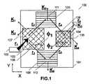
本発明の目的は、入力格子103と、出力格子104と、折畳格子射出瞳孔エクスパンダ105、106とを含む、導波管101を備える、導波管デバイスが提供される、図1に図示される第1の実施形態100において達成される。入力格子は、ベクトルr1によって示される方向において、光を外部光源102から受信する。An object of the present invention is to provide a waveguide device comprising a
いくつかの実施形態では、外部光は、非偏光であり得る。以降に議論されるように、本発明のディスプレイ用途では、光源は、入力画像ノード(IIN)を備え、画像変調された光を提供し得る。本発明のディスプレイ用途では、入力格子は、通常、コリメートされた光をIINから受容し、第1の表面と第2の表面との間の全内部反射を介して、折畳格子まで、光を導波管内で進行させるように構成されるであろう。 In some embodiments, the external light can be unpolarized. As discussed below, in display applications of the present invention, the light source may include an input image node (IIN) to provide image-modulated light. In the display applications of the present invention, the input grid typically receives collimated light from the IIN and transfers the light to the folding grid through total internal reflection between the first and second surfaces. It will be configured to travel within the waveguide.
本明細書で使用されるように、用語「格子」は、いくつかの実施形態では、格子のセットから構成される格子を包含してもよい。例えば、いくつかの実施形態では、入力格子および出力格子はそれぞれ、単一層の中に多重化された2つまたはそれを上回る格子を備える。1つを上回るホログラフィック処方が単一ホログラフィック層の中に記録され得ることが、ホログラフの文献において明確に立証されている。そのような多重化されたホログラムを記録するための方法は、当業者に周知である。いくつかの実施形態では、入力格子および出力格子はそれぞれ、接触するか、または1つもしくはそれを上回る薄い光学基板によって垂直に分離される、2つの重複する格子層を備えてもよい。いくつかの実施形態では、格子層は、ガラスまたはプラスチック基板間に狭装される。いくつかの実施形態では、2つまたはそれを上回るそのような格子層は、全内部反射が外側基板および空気界面に生じる、スタックを形成してもよい。いくつかの実施形態では、導波管は、1つのみの格子層を備えてもよい。いくつかの実施形態では、電極が、基板の面に適用され、格子を回折状態とクリア状態との間で切り替えてもよい。スタックはさらに、ビーム分割コーティングおよび環境保護層等の付加的層を備えてもよい。図1に示される入力および出力格子は、前述の格子構成のいずれかによって提供されてもよい。有利には、入力および出力格子は、共通表面格子ピッチを有するように設計される。 As used herein, the term "lattice" may include, in some embodiments, a grid composed of a set of grids. For example, in some embodiments, the input grid and the output grid each include two or more multiplexed grids in a single layer. It is clearly demonstrated in the holographic literature that more than one holographic formulation can be recorded in a single holographic layer. Methods for recording such multiplexed holograms are well known to those of skill in the art. In some embodiments, the input and output grids may each have two overlapping grid layers that are in contact or vertically separated by one or more thin optical substrates. In some embodiments, the grid layers are narrowed between glass or plastic substrates. In some embodiments, two or more such lattice layers may form a stack in which total internal reflection occurs at the outer substrate and the air interface. In some embodiments, the waveguide may include only one grid layer. In some embodiments, electrodes may be applied to the surface of the substrate to switch the grid between diffracted and clear states. The stack may further include additional layers such as a beam split coating and an environmental protection layer. The input and output grids shown in FIG. 1 may be provided by any of the grid configurations described above. Advantageously, the input and output grids are designed to have a common surface grid pitch.
本発明において使用される入力格子の重要な特徴は、それらが、各格子が入射非偏光光の特定の偏光を導波管経路の中に回折するように配向される、格子を組み合わせることである。出力格子は、類似方式において構成され、したがって、導波管経路からの光は、組み合わせられ、非偏光光として導波管から結合される。図1の実施形態では、入力格子および出力格子はそれぞれ、直交偏光状態のためのピーク回折効率を伴う、交差された格子を組み合わせる。いくつかの実施形態では、偏光状態は、S−偏光およびP−偏光される。いくつかの実施形態では、偏光状態は、円形偏光の逆の意味である。いくつかの実施形態では、所定の偏光状態に作用する2つを上回る格子がそれぞれ、組み合わせられてもよい。この点において、SBG等の液晶ポリマーシステム内に記録される格子の利点は、その固有の複屈折に起因して、それらが強力な偏光選択性を呈することである。しかしながら、一意の偏光状態を提供するように構成され得る、他の格子技術が、使用されてもよい。各格子は、ブラッグ格子の場合、ブラッグフリンジに対して垂直であるベクトルとして定義される、3D空間内の格子ベクトル(またはK−ベクトル)によって特徴付けられる。格子ベクトルは、所与の範囲の入力および回折される角度に関する光学効率を決定する。 An important feature of the input grids used in the present invention is that they combine grids in which each grid is oriented to diffract a particular polarization of incident unpolarized light into the waveguide path. .. The output grid is constructed in a similar fashion so that the light from the waveguide path is combined and coupled from the waveguide as unpolarized light. In the embodiment of FIG. 1, the input grid and the output grid each combine crossed grids with peak diffraction efficiencies for orthogonally polarized states. In some embodiments, the polarization state is S-polarized and P-polarized. In some embodiments, the polarized state is the opposite of circularly polarized light. In some embodiments, more than two grids acting on a given polarization state may be combined, respectively. In this regard, the advantage of lattices recorded in liquid crystal polymer systems such as SBG is that they exhibit strong polarization selectivity due to their inherent birefringence. However, other lattice techniques may be used that may be configured to provide a unique polarization state. Each grid is characterized by a grid vector (or K-vector) in 3D space, which in the case of the Bragg grid is defined as a vector perpendicular to the Bragg fringe. The lattice vector determines the optical efficiency with respect to the input and diffracted angles in a given range.
図1では、入力格子は、格子ベクトルK1、K2を有する、交差された傾斜格子107、108から形成され、格子フリンジは、相対的角度φ1において導波管平面で回転(またはクロック)され、出力格子は、格子ベクトルK3、K4を有する、交差された傾斜格子109、110から形成され、格子フリンジは、相対的角度φ2において導波管平面で回転(またはクロック)される。折畳格子は、格子ベクトルK5、K6を有する、傾斜格子111、112を含む。いくつかの実施形態では、角度φ1およびφ2はそれぞれ、90度と等しい。いくつかの実施形態では、角度φ1およびφ2は、90度未満であってもよい。方向r1に沿って入力格子に入射する入力光の第1の偏光成分は、格子107によって、方向r2に沿ってTIR経路の中に指向され、第2の偏光成分は、第2の格子108によって、方向r3に沿って第2のTIR経路の中に指向される。経路r2、r3に沿った光は、折畳格子105、106によって拡張され(図面のXY平面において)、出力格子に向かってTIR経路r4、r5の中に回折される。図2は、図1の入力格子の3次元図である。図2Aは、多重化された格子が入力格子内で使用される、一実施形態の詳細を示す。図2Aは、格子108の4つの格子フリンジ120と、格子107の4つの格子フリンジ121とを示す。図2Bは、1つのフリンジ122が格子傾斜角度θ1に図示される、格子ベクトルK3を含む、平面X’Y’における断面図を示す。いくつかの実施形態では、入力格子内の格子は、同じ傾斜角度および格子ピッチを有する。いくつかの実施形態では、図1に図示される格子レイアウトおよびビーム伝搬経路は、X軸を中心として対称である。In Figure 1, an input grating has a grating vectorK1,K2, is formed from a
図3は、図1の導波管デバイスの断面130であって、導波管131と、入力格子103と、出力格子104と、折畳格子105のうちの1つとを示す。入力光線1000、入力格子と出力格子との間の全内部反射(TIR)経路1001、および出力格子によって導波管から外部結合される光線1002、1003が、図示される。 FIG. 3 is a
いくつかの実施形態では、折畳格子は、XまたはY軸に対して45°にクロック(すなわち、導波管平面において傾斜)され、折畳された光のための適正な角度帯域幅を確実にする。しかしながら、本発明のいくつかの実施形態は、他のクロック角度を使用して、ディスプレイの人間工学的設計において生じ得る、格子の位置付けに関する空間制約を満たしてもよい。 In some embodiments, the folding grid is clocked at 45 ° with respect to the X or Y axis (ie, tilted in the waveguide plane) to ensure proper angular bandwidth for the folded light. To. However, some embodiments of the present invention may use other clock angles to satisfy the spatial constraints on grid positioning that may occur in the ergonomic design of the display.
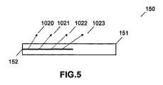
図1の実施形態では、各格子は、固定されたベクトルを有する。いくつかの実施形態では、入力および出力格子のうちの少なくとも1つは、回転k−ベクトルを有する。K−ベクトルを回転させることは、導波管厚を増加させることを必要とせず、格子の角度帯域幅が拡張されることを可能にする。図4は、K−ベクトル1010−1013を有する離散格子要素142−145を含む、導波管部分141を備える、回転K−ベクトル格子140を図示する。図5に図示されるもの等のいくつかの実施形態では、回転K−ベクトル格子は、K−ベクトルが図示される方向1020−1023を含む方向における平滑単調変動を受ける、単一格子要素152を含む、導波管部分151を備える。図4−5に図示されるタイプの回転K−ベクトル格子は、前述の格子のいずれか内に実装されることができる。 In the embodiment of FIG. 1, each grid has a fixed vector. In some embodiments, at least one of the input and output grids has a rotation k-vector. Rotating the K-vector does not require increasing the waveguide thickness and allows the angular bandwidth of the grid to be extended. FIG. 4 illustrates a rotating K-
本発明の原理および教示は、参照することによって本明細書に組み込まれる参考文献に開示されるような本発明者らによる他の導波管発明と組み合わせて、多くの異なるディスプレイおよびセンサデバイスにおいて適用されてもよい。図6における実施形態に基づく、いくつかの実施形態では、導波管デバイス160は、導波管161と、ベクトル方向r7における入力光源162とを備える。導波管は、入力格子163と、傾斜格子167を含む第1の出力格子166と、格子169を含む第2の出力格子168とを含む。第1の偏光成分は、多重格子163によって、方向r8に沿って第1の出力格子に向かって第1のTIR経路の中に指向され、第2の偏光成分は、第2の多重格子164によって、方向r9に沿って第2の出力格子に向かって第2のTIR経路の中に指向される。光は、次いで、第1および第2の出力格子によって、方向r10およびr11に導波管から抽出される。出力光は、異なる偏光を有し、これは、所望に応じて、出力格子のうちの1つにわたって設置された半波プレートを用いて、共通偏光に調節されることができる。図7に示されるもの等のいくつかの実施形態では、図6のものに類似する導波管構成が、導波管センサ内で使用されてもよい。導波管デバイス170は、傾斜格子174を含む第1の入力格子173と、傾斜格子176を含む第2の入力格子175と、交差された多重化された傾斜格子178、179を含む出力格子177とを含む、導波管171を備える。図7の検討から、光学構成は、図6のものに非常に類似するが、光線経路は、逆転され、図6の光源は、検出器172に取って代わることが明白となるはずである。第1および第2の方向r12、r14における入射光は、第1および第2の入力格子によって、TIR経路r13、r15内で出力格子に向かって回折される。経路は、第1の偏光状態を有し、かつ経路は、第2の偏光状態を有する。出力格子は、2つのTIR経路からの光を導波管から方向r16に検出器に向かって回折する。特定の偏光の光が検出されるために、半波プレートが、入力格子のうちの1つにわたって設置される。The principles and teachings of the present invention apply in many different display and sensor devices in combination with other waveguide inventions by us as disclosed in the references incorporated herein by reference. May be done. Based on the embodiment in FIG. 6, in some embodiments, the
格子の数は、2つを上回ることができる。例えば、図8の実施形態では、入力格子は、K−ベクトルK7、K8、K9を有する、3つの多重化された格子と、K−ベクトルK10、K11、K12を有する、折畳格子とを備え、出力格子は、K−ベクトルK13、K14、K15を伴う、3つの多重化された格子を備える。K−ベクトルK7、K10、K13を伴う格子は、光線方向r24に導波管に入射する光を光学経路r18、r21、およびr19、r22、およびr20、r23の中に回折する。K−ベクトルK8、K11、K14を伴う格子は、光学経路r19、r22を画定する。K−ベクトルK9、K12K15を伴う格子は、光学経路r20、r23を画定する。出力格子は、3つの経路からの光を出力方向r24に組み合わせる。The number of grids can exceed two. For example, in the embodiment of FIG. 8, the input grid has three multiplexed grids withK-vectors K7 ,K 8 ,K9and K-vectors K10 ,K11 ,K12 . With a folding grid, the output grid comprises three multiplexed grids withK-vectors K13 ,K 14 , andK15. The lattice with theK -vectorsK7 ,K 10 , andK13 directs the light incident on the waveguide in theray direction r24into optical paths r18 ,r21 , andr19 ,r22 , andr20 ,r23. Diffract in. The lattice with theK -vectorsK8 ,K 11 andK14 defines theoptical paths r19 andr22. A grid withK -vectorsK9 andK 12K15 defines theoptical paths r20 andr23. The output grating combines light from the three paths in the output directionr24.
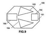
入力、折畳、または出力格子の形状は、導波管用途に依存し、要求されるビーム拡張、出力ビーム幾何学形状、ビーム均一性、および人間工学的要因等の要因に従って、任意の多角形幾何学形状であり得る。図9は、折畳格子が三角形幾何学形状である、一実施形態190を示す。導波管191は、入力格子191と、折畳格子193、194と、出力格子195とを含む。 The shape of the input, fold, or output grid depends on the waveguide application and is any polygon, depending on factors such as required beam expansion, output beam geometry, beam uniformity, and ergonomic factors. It can be a geometric shape. FIG. 9 shows one
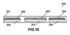
液晶ポリマー材料系内に記憶される格子を使用する、いくつかの実施形態では、折畳格子、入力格子、または出力格子のうちの少なくとも1つに重複する、少なくとも1つの偏光制御層が、任意の格子、特に、本発明者らが偏光回転をもたらし得ることを見出した、折畳格子内の偏光回転を補償する目的のために提供されてもよい。図10は、導波管デバイスが、入力格子202と、折畳格子203と、出力格子204とを備える、導波管201を備える、1つのそのような実施形態を図示する。いくつかの実施形態では、格子は全て、202−204によって参照されるもの等の偏光制御層によってオーバーレイされる。いくつかの実施形態では、偏光制御層は、折畳格子のみまたは任意の他の格子のサブセットに適用される。偏光制御層は、光学リターダフィルムを備えてもよい。HPDLC材料に基づく、いくつかの実施形態では、格子の複屈折が、導波管デバイスの偏光性質を制御するために使用されてもよい。設計変数としてのHPDLC格子の複屈折テンソル、K−ベクトル、および格子占有面積の使用は、導波管デバイスの角度能力および光学効率を最適化するための設計空間を開放する。 In some embodiments that use a grid stored within the liquid crystal polymer material system, at least one polarization control layer that overlaps at least one of the folding grid, input grid, or output grid is optional. Grids, in particular, may be provided for the purpose of compensating for polarization rotation within a folding grid, which we have found to result in polarization rotation. FIG. 10 illustrates one such embodiment in which the waveguide device comprises a
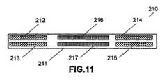
いくつかの実施形態では、入力、出力、および折畳格子は、導波管内の別個の層に記録されてもよい。例えば、図11に示される2層設計では、導波管211は、別個の重複する格子層212、213を備える入力格子と、重複する層214、215を備える、出力格子と、折畳格子(非重複)216、217とを備える。 In some embodiments, the inputs, outputs, and folding grids may be recorded in separate layers within the waveguide. For example, in the two-layer design shown in FIG. 11, the
図12のうちの1つ等のいくつかの実施形態では、図11のアーキテクチャは、別個の導波管を使用して実装されてもよい。導波管は、典型的には、空隙または低屈折率光学材料の薄層によって分離される。図12に示される実施形態220では、第1の導波管221は、入力格子223と、折畳格子224と、出力格子225とを含有し、第2の導波管222は、入力格子226と、折畳格子227と、出力格子228とを含む。いくつかの実施形態では、第1の導波管は、第1の入力−折畳−出力格子経路を提供し、第2の導波管は、第2の入力−折畳−出力格子経路を提供する。 In some embodiments, such as one of FIG. 12, the architecture of FIG. 11 may be implemented using separate waveguides. Waveguides are typically separated by voids or a thin layer of low index optical material. In
図1の実施形態および以下に説明される実施形態では、入力、折畳、および出力格子のうちの少なくとも1つは、電気的に切替可能であってもよい。多くの実施形態では、全3つの格子タイプは、受動的である、すなわち、非切替式であることが望ましい。 In the embodiment of FIG. 1 and the embodiments described below, at least one of the input, folding, and output grids may be electrically switchable. In many embodiments, it is desirable that all three grid types be passive, i.e. non-switchable.
いくつかの実施形態では、入力格子、折畳格子、および出力格子は、切替可能または切替可能でないブラッグ格子等のホログラフィック格子である。いくつかの実施形態では、SBGとして具現化される、入力カプラ、折畳格子、および出力格子は、ホログラフィックポリマー分散液晶(HPDLC)(例えば、液晶液滴のマトリクス)内に記録されるブラッグ格子であることができるが、SBGはまた、他の材料内に記録されてもよい。一実施形態では、SBGは、液体ポリマー中に分散される固体液晶のマトリクスを有する、POLICRYPSまたはPOLIPHEM等の均一変調材料内に記録される。SBGは、性質上、切替または非切替式であることができる。その非切替形態では、SBGは、その液晶成分に起因して、高屈折率変調を提供可能な従来のホログラフィックフォトポリマー材料に優る利点を有する。例示的均一変調液晶ポリマー材料系は、Caputo et alによる米国特許出願公開第US2007/0019152号およびStumpe et al.によるPCT出願第PCT/EP2005/006950号に開示されており、両方とも、参照することによってその全体として本明細書に組み込まれる。均一変調格子は、高屈折率変調(故に、高回折効率)および低散乱によって特徴付けられる。いくつかの実施形態では、入力カプラ、折畳格子、および出力格子は、反転モードHPDLC材料内に記録される。反転モードHPDLCは、格子が、電場が印加されないとき、受動的であって、電場の存在下では、回折性となるという点において、従来のHPDLCと異なる。反転モードHPDLCは、「IMPROVEMENTS TO HOLOGRAPHIC POLYMER DISPERSED LIQUID CRYSTAL MATERIALS AND DEVICES」と題されたPCT出願PCT/GB2012/000680号に開示されるレシピおよびプロセスのいずれかに基づいてもよい。格子は、前述の材料系のいずれかに記録されるが、受動(非切替)モードで使用されてもよい。受動格子を液晶ポリマー材料内に記録する利点は、最終ホログラムが液晶によって与えられる高屈折率変調から利益を享受することである。より高い屈折率変調は、高回折効率および広角帯域幅に変換される。製作プロセスは、切替のために使用されるものと同じであるが、電極コーティング段階が省略される。LCポリマー材料系は、その高屈折率変調に照らして、非常に望ましい。いくつかの実施形態では、格子は、HPDLC内に記録されるが、切り替えられない。 In some embodiments, the input grid, folding grid, and output grid are holographic grids, such as Bragg grids that are switchable or non-switchable. In some embodiments, the input couplers, folding grids, and output grids, embodied as SBGs, are Bragg grids recorded within a holographic polymer dispersed liquid crystal (HPDLC) (eg, a matrix of liquid crystal droplets). Although it can be, the SBG may also be recorded in other materials. In one embodiment, the SBG is recorded in a uniform modulation material such as POLICRYPS or POLIPHEM, which has a matrix of solid liquid crystals dispersed in a liquid polymer. SBGs can, by their nature, be switchable or non-switchable. In its non-switchable form, SBG has advantages over conventional holographic photopolymer materials capable of providing high index of refraction modulation due to its liquid crystal components. Exemplary uniformly modulated liquid crystal polymer material systems are described in US Patent Application Publication No. US2007 / 0019152 by Caputo et al. PCT application No. PCT / EP2005 / 006950, both of which are incorporated herein by reference in their entirety. Uniform modulation grids are characterized by high index modulation (hence high diffraction efficiency) and low scattering. In some embodiments, the input coupler, folding grid, and output grid are recorded within the inverted mode HPDLC material. Inversion mode HPDLC differs from conventional HPDLC in that the grid is passive when no electric field is applied and is diffractible in the presence of an electric field. The inversion mode HPDLC may be based on any of the recipes and processes disclosed in PCT application PCT / GB2012 / 00680, entitled "IMPROVEMENTS TO HOLOGRAPHIC POLYMER DISPERSED LIQUID CRYSTAL MATERIALS AND DEVICES". The grid is recorded in any of the material systems described above, but may be used in passive (non-switching) mode. The advantage of recording a passive lattice in a liquid crystal polymer material is that the final hologram benefits from the high index of refractive index modulation provided by the liquid crystal. Higher index of refraction modulation translates into higher diffraction efficiency and wide-angle bandwidth. The fabrication process is the same as that used for switching, but the electrode coating step is omitted. LC polymer material systems are highly desirable in light of their high index modulation. In some embodiments, the grid is recorded in the HPDLC but cannot be switched.
図13−14に図示されるもの等のいくつかの実施形態では、本発明は、導波管を通して異なるスペクトル帯域幅の少なくとも2つのビームを伝搬するための手段を提供する。 In some embodiments, such as those illustrated in FIGS. 13-14, the present invention provides means for propagating at least two beams of different spectral bandwidth through a waveguide.
図13は、光源232に結合される図1のうちの1つと類似アーキテクチャの導波管230を備える、実施形態230の平面図である。入力格子233および出力格子234はそれぞれ、直交偏光状態、典型的には、S−偏光およびP−偏光のためのピーク回折効率を伴う、交差された格子を組み合わせる。図1では、入力格子は、格子ベクトルK21、K22を有する、交差された傾斜格子237、238から形成され、格子フリンジは、相対的角度φ3において導波管平面で回転(またはクロック)され、出力格子は、格子ベクトルK23、K24を有する、交差された傾斜格子239、240から形成され、格子フリンジは、相対的角度φ4において導波管平面で回転(またはクロック)される。折畳格子235、236は、格子ベクトルK25、K26を有する、傾斜格子241、242を含む。いくつかの実施形態では、角度φ3およびφ4はそれぞれ、90度と等しい。方向r31に沿って入力格子に入射する波長λ1を伴う源からの入力光の第1の偏光成分は、格子107によって、方向r32に沿ってTIR経路の中に指向される。波長λ2を伴う第2の偏光成分は、第2の格子108によって、方向r33に沿って第2のTIR経路の中に指向される。経路r32、r33に沿った光は、折畳格子によって拡張され(図面のXY平面に)、出力格子に向かってTIR経路r34およびr35の中に回折される。図14は、図13の導波管の断面図を示し、入力格子233と、出力格子234と、折畳格子235のうちの1つとを示す。波長λ1の光のための光線経路r31、r32、r33は、図14では、光線1030−1032によって表され、出力光は、1033によって示される(図13では、r36)。その波長の光の第1の偏光成分およびその波長の光の第2の成分のみが、導波管の中に結合されるため、図13−14の実施形態は、50%を上回らない光学効率を有し得る。導波管の中に結合されない光は、図14における光線1034によって示されるように、実質的逸脱を伴わずに、入力格子を通して伝搬するであろう。図13−14の実施形態は、FIG. 13 is a plan view of
一実施形態250では、偏光復元のための手段を含む、図13−14の実施形態に基づく、1つを上回る色の光を伝搬するための導波管が、提供される。上記に説明されるように、交差された入力格子を使用することによって、我々は、各入力光偏光が、交差された格子のうちの1つによって、回折のために正しく整合されることを確実にする。カラー導波管用途では、我々は、少なくとも2つの入力偏光と、少なくとも2つの色成分とを有する。故に、我々は、2つの交差された格子層を要求する。実施形態250における導波管は、2つの接合された基板を備え、その下側のものは、本質的に、図13−14の導波管231であって、上側のもの251は、下側基板の入力格子にオーバーレイする入力格子252を含む。上側および下側入力格子は、半波リターダフィルム253を狭装する。上側基板内の入力格子は、格子ベクトルK27、K28を有する、交差された傾斜格子253、254から形成され、格子フリンジは、相対的角度φ5において導波管平面で回転(またはクロック)される。In one
図16は、実施形態250の断面図を示し、上側基板251と、下側基板231とを示し、入力格子233と、出力格子234と、折畳格子235のうちの1つとを含む。ここでは、基板251の上側表面と基板231の下側表面との間のTIR経路に対応する、図13に示されるような波長λ2の光のための光線経路r31、r32、r33は、図16では、光線1040−1042によって表される。入力格子233によって回折されない光は、光1042として上向きに伝搬し、上側基板の入力格子によって回折される。方向r36に沿って入力格子に入射する波長λ1を伴う入力光の第1の偏光成分(図16では、1044によって示される)は、格子253によって、方向r37に沿ってTIR経路の中に指向され、波長λ2を伴う第2の偏光成分は、第2の格子254によって、方向r38に沿って第2のTIR経路の中に指向される。TIR経路は、基板251の上側表面と基板231の下側表面との間に生じる。導波管からの出力光は、下側基板の入力格子によって回折される光の場合、1047によって、下側基板の入力格子によって回折される光の場合、1948によって示される。要するに、実施形態250は、2つの重要な利点を提供する。第1に、異なる色の光のための別個のクロストークのない導波管経路を提供する。第2に、任意の偏光状態の光の利用を可能にし、SBG等の液晶ベースの格子が基本的に偏光敏感であるという限界を克服する。入力格子後の全ての導波管誘導光が、折畳および出力格子による回折のための補正偏光(SBGの場合、P−偏光)にあるため、1つのみの出力格子層が、要求される。FIG. 16 shows a cross-sectional view of
図13−16に図示されるもの等に基づく、いくつかの実施形態では、第1の波長は、赤色光に対応し、第2の波長は、青緑色光に対応する。いくつかの実施形態では、入力および出力格子は、2つを上回る格子を組み合わせてもよく、各格子は、一意の偏光状態および一意のスペクトル帯域幅に作用する。いくつかの実施形態では、入力および出力格子は、2つを上回る格子を組み合わせてもよく、各格子は、一意の偏光状態、一意の回折効率角度帯域幅、および一意のスペクトル帯域幅で作用する。 In some embodiments, such as those illustrated in FIGS. 13-16, the first wavelength corresponds to red light and the second wavelength corresponds to blue-green light. In some embodiments, the input and output grids may be a combination of more than two grids, with each grid acting on a unique polarization state and a unique spectral bandwidth. In some embodiments, the input and output grids may be a combination of more than two grids, each grid acting with a unique polarization state, a unique diffraction efficiency angular bandwidth, and a unique spectral bandwidth. ..
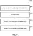
図17のフロー図に図示される一実施形態では、1つを上回る偏光成分の光を導波管の中に結合する方法が、提供される。フロー図を参照すると、該方法は、以下のステップを含むことが分かる。 In one embodiment illustrated in the flow diagram of FIG. 17, a method of coupling light of more than one polarizing component into a waveguide is provided. With reference to the flow chart, it can be seen that the method involves the following steps:
ステップ2001では、交差された第1および第2の格子を備える入力格子を含む、導波管を提供する。
ステップ2002では、光源を導波管に結合する。 In
ステップ2003では、第1の格子が、光の第1の偏光状態を第1の導波管経路の中に回折する。 In
ステップ2004では、ステップ2004と同時に、第1の格子が、光の第2の偏光状態を第2の導波管経路の中に回折する。 In
図18のフロー図に図示される一実施形態では、1つを上回る偏光成分の光を導波管の中に結合する方法2010が、提供される。 In one embodiment illustrated in the flow diagram of FIG. 18, a
フロー図を参照すると、該方法は、以下のステップを含むことが分かる。 With reference to the flow chart, it can be seen that the method involves the following steps:
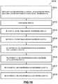
ステップ2011では、交差された第1および第2の格子を備える、入力格子と、第1および第2の折畳格子と、交差された第3および第4の格子を備える、出力格子とを含む、導波管を提供する。
ステップ2012では、光源を導波管に結合する。 In
ステップ2013では、第1の格子が、光の第1の偏光状態を第1の導波管経路の中に回折する。 In
ステップ2014では、ステップ2004と同時に、第1の格子が、光の第2の偏光状態を第2の導波管経路の中に回折する。 In
ステップ2015では、第1の折畳格子が、第1の導波管経路からの光を、第3の導波管経路の中に、そして出力格子まで回折する。 In
ステップ2016では、ステップ2015と同時に、第2の折畳格子が、第2の導波管経路内の光を、第4の導波管経路の中に、そして出力格子まで回折する。 In
ステップ2017では、第3の格子が、第3の導波管経路内の光を導波管から回折する。 In
ステップ2018では、ステップ2017と同時に、第4の格子が、第4の導波管経路内の光を導波管から回折する。 In
図19のフロー図に図示される一実施形態では、1つを上回る偏光成分および1つを上回る色の光を導波管の中に結合する方法2020が、提供される。フロー図を参照すると、該方法は、以下のステップを含むことが分かる。 In one embodiment illustrated in the flow diagram of FIG. 19, a
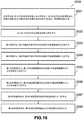
ステップ2021では、交差された第1および第2の格子を備える、入力格子と、第1および第2の折畳格子と、交差された第3および第4の格子を備える、出力格子とを含む、導波管を提供する。
ステップ2022では、第1および第2の色の光源を導波管に結合する。 In
ステップ2023では、第1の格子が、光の第1の色の第1の偏光状態を第1の導波管経路の中に回折する。 In
ステップ2024では、ステップ2004と同時に、第1の格子が、第2の色の光の第2の偏光状態を第2の導波管経路の中に回折する。 In
ステップ2025では、第1の折畳格子が、第1の導波管経路からの光を、第3の導波管経路の中に、そして出力格子まで回折する。 In
ステップ2026では、ステップ2015と同時に、第2の折畳格子が、第2の導波管経路内の光を、第4の導波管経路の中に、そして出力格子まで回折する。 In
ステップ2027では、第3の格子が、第3の導波管経路内の光を導波管から回折する。 In
ステップ2028では、ステップ2017と同時に、第4の格子が、第4の導波管経路内の光を導波管から回折する。 In
図20のフロー図に図示される一実施形態では、1つを上回る偏光成分および1つを上回る色の光を導波管の中に結合する方法2030が、提供される。フロー図を参照すると、該方法は、以下のステップを含むことが分かる。 In one embodiment illustrated in the flow diagram of FIG. 20, a
ステップ2031では、交差された第1および第2の格子を備える入力格子を、第1および第2の折畳格子、ならびに交差された第3および第4の格子を備える、出力格子含む、第1の基板と、交差された第5および第6の格子を備える入力格子を含む、第2の基板と、入力格子によって狭装される、半波リターダフィルムとを備える、導波管を提供する。 In
ステップ2032では、第1および第2の色の光源を導波管に結合する。 In
ステップ2033では、第1および第5の格子が、光の第1の色の第1の偏光状態を第1の導波管経路の中に回折する。 In
ステップ2034では、ステップ2004と同時に、第2および第6の格子が、光の第2の色の第2の偏光状態を第2の導波管経路の中に回折する。 In
ステップ2035では、第1の折畳格子が、第1の導波管経路からの光を、第3の導波管経路の中に、そして出力格子まで回折する。 In
ステップ2036では、ステップ2015と同時に、第2の折畳格子が、第2の導波管経路内の光を、第4の導波管経路の中に、そして出力格子まで回折する。 In
ステップ2037では、第3の格子が、第3の導波管経路内の光を導波管から回折する。 In
ステップ2038では、ステップ2017と同時に、第4の格子が、第4の導波管経路内の光を導波管から回折する。 In
本発明のディスプレイ用途では、本装置は、通常、導波管に光学的に結合される、入力画像ノード(IIN)をさらに備え得る。典型的には、IINは、マイクロディスプレイパネルと、光源と、ディスプレイパネルを照明し、反射された光を分離し、それを要求されるFOVにコリメートするために必要とされる、光学コンポーネントとを統合する。本発明は、任意の特定のマイクロディスプレイ技術を仮定しない。いくつかの実施形態では、マイクロディスプレイパネルは、液晶デバイスまたはMEMSデバイスである。いくつかの実施形態では、マイクロディスプレイは、有機発光ダイオード(OLED)技術に基づいてもよい。そのような発光型デバイスは、別個の光源を要求せず、したがって、より小さい形状因子の利点をもたらすであろう。いくつかの実施形態では、IINは、走査される変調されたレーザに基づいてもよい。IINは、いくつかの実施形態によると、各ディスプレイピクセルが、基板導波管内の一意の角度方向に変換されるように、マイクロディスプレイパネル上に表示される画像を投影させる。IIN内に含有されるコリメーション光学は、レンズおよびミラーを備えてもよく、これは、いくつかの実施形態は、回折レンズおよびミラーであってもよい。いくつかの実施形態では、IINは、「HOLOGRAPHIC WIDE ANGLE DISPLAY」と題された米国特許出願第13/869,866号および「TRANSPARENT WAVEGUIDE DISPLAY」と題された米国特許出願第13/844,456号に開示される、実施形態および教示に基づいてもよい。いくつかの実施形態では、IINは、光をマイクロディスプレイ上に指向し、反射された光を導波管に向かって透過させるためのビームスプリッタを含む。一実施形態では、ビームスプリッタは、HPDLC内に記憶された格子であって、そのような格子の固有の偏光選択性を使用して、ディスプレイを照明する光と、ディスプレイから反射された画像変調された光とを分離する。いくつかの実施形態では、ビームスプリッタは、偏光ビームスプリッタ立方体である。いくつかの実施形態では、IINは、デスペックラを組み込む。有利には、デスペックラは、「LASER ILLUMINATION DEVICE」と題された米国特許第8,565,560号の実施形態および教示に基づくホログラフィック導波管デバイスである。光源は、レーザまたはLEDであることができ、照明ビーム角度特性を修正するための1つまたはそれを上回るレンズを含むことができる。画像源は、マイクロディスプレイまたはレーザベースのディスプレイであることができる。LEDは、レーザより均一性を提供し得る。レーザ照明が、使用される場合、照明帯域固定が導波管出力に生じるリスクがある。いくつかの実施形態では、導波管内のレーザ照明帯域固定は、「METHOD AND APPARATUS FOR GENERATING INPUT IMAGES FOR HOLOGRAPHIC WAVEGUIDE DISPLAYS」と題された米国仮特許出願第62/071,277号に開示される技法および教示を使用して克服することができる。いくつかの実施形態では、光源101からの光は、偏光される。1つまたはそれを上回る実施形態では、画像源は、液晶ディスプレイ(LCD)マイクロディスプレイまたは液晶オンシリコン(LCoS)マイクロディスプレイである。 In the display applications of the present invention, the device may further comprise an input image node (IIN), which is usually optically coupled to a waveguide. Typically, the IIN provides a microdisplay panel, a light source, and the optical components needed to illuminate the display panel, separate the reflected light, and collimate it with the required FOV. Integrate. The present invention does not assume any particular microdisplay technology. In some embodiments, the microdisplay panel is a liquid crystal device or a MEMS device. In some embodiments, the microdisplay may be based on organic light emitting diode (OLED) technology. Such luminescent devices do not require a separate light source and will therefore offer the advantage of smaller Scherrer equations. In some embodiments, the IIN may be based on a modulated laser being scanned. The IIN projects an image displayed on a microdisplay panel such that each display pixel, according to some embodiments, is transformed into a unique angular direction within the substrate waveguide. The collimation optics contained within the IIN may include a lens and a mirror, which in some embodiments may be a diffractive lens and a mirror. In some embodiments, IIN is a US Patent Application No. 13 / 869,866 entitled "HOLOGRAPHIC WIDE ANGLE DISPLAY" and a US Patent Application No. 13 / 844,456 entitled "TRANSPARENT WAVEGUIDE DISPLAY". May be based on embodiments and teachings disclosed in. In some embodiments, the IIN includes a beam splitter for directing light onto the microdisplay and propagating the reflected light towards the waveguide. In one embodiment, the beam splitter is a grid stored in HPDLC that uses the inherent polarization selectivity of such a grid to be used to illuminate the display and image-modulate the light reflected from the display. Separate from the light. In some embodiments, the beam splitter is a polarized beam splitter cube. In some embodiments, the IIN incorporates a despecra. Advantageously, the Despecra is a holographic waveguide device based on the embodiments and teachings of US Pat. No. 8,565,560 entitled "LASER ILLUMINATION DEVICE". The light source can be a laser or LED and can include one or more lenses for modifying the illumination beam angle characteristic. The image source can be a microdisplay or a laser-based display. LEDs may provide more uniformity than lasers. When laser illumination is used, there is a risk that illumination band fixation will occur at the waveguide output. In some embodiments, fixing the laser illumination band in the waveguide is a technique disclosed in US Provisional Patent Application No. 62/071,277 entitled "METHOD AND APPARATUS FOR GENERATING INPUT IMAGES FOR HOLOGRAPHIC WAVEGUIDE DISPLAYS". And can be overcome using teaching. In some embodiments, the light from the
いくつかの実施形態では、折畳格子角度帯域幅は、格子処方を誘導された光と格子の二重相互作用を促進するように設計することによって向上されることができる。二重相互作用折畳格子の例示的実施形態は、「WAVEGUIDE GRATING DEVICE」と題された米国特許出願第14/620,969号に開示されている。 In some embodiments, the folding lattice angular bandwidth can be improved by designing the lattice formulation to facilitate the dual interaction of the induced light and lattice. An exemplary embodiment of a dual-interaction folding lattice is disclosed in US Patent Application No. 14 / 620,969 entitled "WANGEGUIDE GRATING DEVICE".
いくつかの実施形態では、入力、折畳、または出力格子のうちの少なくとも1つは、表面起伏構造に基づいてもよい。 In some embodiments, at least one of the input, folding, or output grids may be based on a surface undulation structure.
いくつかの実施形態では、入力、折畳、または出力格子のうちの少なくとも1つは、2つまたはそれを上回る角度回折処方を組み合わせ、角度帯域幅を拡張させてもよい。同様に、いくつかの実施形態では、入力、折畳、または出力格子のうちの少なくとも1つは、2つまたはそれを上回るスペクトル回折処方を組み合わせ、スペクトル帯域幅を拡張させてもよい。例えば、色多重化された格子が、使用され、原色のうちの2つまたはそれを上回るものを回折してもよい。 In some embodiments, at least one of the input, folding, or output grids may be combined with two or more angular diffraction formulations to extend the angular bandwidth. Similarly, in some embodiments, at least one of the input, folding, or output grids may be combined with two or more spectral diffraction formulations to extend the spectral bandwidth. For example, a color-multiplexed grid may be used to diffract two or more of the primary colors.
いくつかの実施形態では、セル基板は、ガラスから製作されてもよい。例示的ガラス基板は、標準的Corning Willowガラス基板(屈折率1.51)であって、これは、50ミクロンまでの厚さにおいて利用可能である。他の実施形態では、セル基板は、光学プラスチックであってもよい。 In some embodiments, the cell substrate may be made of glass. An exemplary glass substrate is a standard Corning Willow glass substrate (refractive index 1.51), which is available in thicknesses up to 50 microns. In other embodiments, the cell substrate may be an optical plastic.
いくつかの実施形態では、格子層は、別個の層に分解されてもよい。例えば、いくつかの実施形態では、第1の層は、折畳格子を含む一方、第2の層は、出力格子を含む。いくつかの実施形態では、第3の層は、入力格子を含むことができる。その層の数は、次いで、単一導波管基板の中にともにラミネートされてもよい。いくつかの実施形態では、格子層は、ともにラミネートされ、単一基板導波管を形成する、入力カプラと、折畳格子と、出力格子(またはその一部)とを含む、いくつかの部品から成る。部品は、部品のものに合致する屈折率の光学糊または他の透明材料によって分離されてもよい。別の実施形態では、格子層は、入力カプラ、折畳格子、および出力格子毎に、所望の格子厚のセルを生成し、各セルをSBG材料で真空充填することによるセル作製プロセスを介して、形成されてもよい。一実施形態では、セルは、入力カプラ、折畳格子、および出力格子のための所望の格子厚を画定する、ガラスのプレート間の間隙を伴って、ガラスの複数のプレートを位置付けることによって形成される。一実施形態では、1つのセルは、別個の開口がSBG材料の異なるポケットで充填されるように、複数の開口を伴って作製されてもよい。任意の介在空間が、次いで、分離材料(例えば、糊、油等)によって分離され、別個の面積を画定してもよい。一実施形態では、SBG材料は、基板上にスピンコーティングされ、次いで、材料の硬化後、第2の基板によって被覆されてもよい。 In some embodiments, the lattice layer may be decomposed into separate layers. For example, in some embodiments, the first layer comprises a folding grid, while the second layer comprises an output grid. In some embodiments, the third layer can include an input grid. The number of layers may then be laminated together in a single waveguide substrate. In some embodiments, the grid layers are laminated together to form a single substrate waveguide, including an input coupler, a folding grid, and an output grid (or part thereof). Consists of. The part may be separated by an optical glue or other transparent material with a refractive index that matches that of the part. In another embodiment, the grid layer produces cells of the desired grid thickness for each input coupler, folding grid, and output grid, via a cell fabrication process by vacuum filling each cell with SBG material. , May be formed. In one embodiment, the cell is formed by positioning multiple plates of glass with gaps between the plates of glass that define the desired grid thickness for the input coupler, folding grid, and output grid. To. In one embodiment, one cell may be made with multiple openings such that separate openings are filled with different pockets of SBG material. Any intervening space may then be separated by a separating material (eg, glue, oil, etc.) to define a separate area. In one embodiment, the SBG material may be spin coated onto a substrate and then coated with a second substrate after the material has cured.
折畳格子を使用することによって、導波管ディスプレイは、いくつかの実施形態によると、有利には、情報を表示する以前のシステムおよび方法より少ない層を要求する。加えて、折畳格子を使用することによって、光は、二重瞳孔拡張を達成しながら、導波管外側表面によって画定された単一長方形プリズム内の導波管の中を全内部反射によって進行することができる。 By using a folding grid, the waveguide display, according to some embodiments, advantageously requires fewer layers than previous systems and methods of displaying information. In addition, by using a folding grid, light travels through the waveguide in a single rectangular prism defined by the outer surface of the waveguide by total internal reflection while achieving double pupil dilation. can do.
いくつかの実施形態では、入力格子、折畳格子、および出力格子は、2つの光の波を基板内のある角度において干渉し、ホログラフィック波正面を生成し、それによって、所望の角度において導波管基板101内に設定される明暗フリンジを生成することによって、生成されることができる。いくつかの実施形態では、所与の層内の格子は、格子面積を横断して記録レーザビームを走査または段階化することによって、段階式方式で記録される。いくつかの実施形態では、格子は、ホログラフィック印刷産業において現在使用されているマスタリングおよび密着印画プロセスを使用して記録される。 In some embodiments, the input grid, folding grid, and output grid interfere the two waves of light at an angle within the substrate to produce a holographic wave front, thereby guiding at the desired angle. It can be generated by generating the light and dark fringes set in the
いくつかの実施形態では、前述の原理に基づく、赤色、緑色、および青色回折格子層が、カラー非偏光照明のために提供されてもよい。いくつかの実施形態では、本発明の原理によるカラー導波管は、各モノクロ導波管内に1つのみの格子層を使用してもよい。いくつかの実施形態では、前述の原理に基づく導波管は、赤外線帯域内で動作する。 In some embodiments, red, green, and blue diffraction grating layers based on the aforementioned principles may be provided for color unpolarized illumination. In some embodiments, color waveguides according to the principles of the invention may use only one grid layer within each monochrome waveguide. In some embodiments, the waveguide based on the aforementioned principle operates in the infrared band.
ディスプレイを対象とする、いくつかの実施形態では、折畳格子は、対角線方向に配向されてもよい。折畳格子は、いくつかの実施形態では、瞳孔拡張を第1の方向に提供し、導波管の内側の全内部反射を介して、光を出力格子に指向するように構成される。一実施形態では、各折畳格子の縦方向縁は、各折畳格子がディスプレイ光の伝搬方向に対して対角線上に設定されるように、入力カプラの整合軸に対して斜めである。折畳格子は、入力カプラからの光が出力格子に再指向されるように角度付けられる。一実施例では、折畳格子は、ディスプレイ画像が入力カプラから放出される方向に対して45の度の角度に設定される。本特徴は、折畳格子を辿って伝搬するディスプレイ画像を出力格子に向けさせる。例えば、一実施形態では、折畳格子は、画像を90度出力格子に向けさせる。このように、単一導波管は、2軸瞳孔拡張を水平および垂直方向の両方に提供する。一実施形態では、折畳格子はそれぞれ、部分的回折構造を有してもよい。出力格子は、瞳孔拡張を第1の方向と異なる第2の方向に提供し、光を第1の表面または第2の表面から導波管を出射させるように構成される。出力格子は、全内部反射を介して、画像を折畳格子から受信し、瞳孔拡張を第2の方向に提供する。いくつかの実施形態では、出力格子は、基板の複数の層から成り、それによって、出力格子の複数の層を備える。故に、格子が導波管内の1つの平面にあるべきという要件は存在せず、格子は、相互の上にスタックされてもよい(例えば、相互の上にスタックされた格子のセル)。 In some embodiments intended for displays, the folding grid may be diagonally oriented. The folding grid, in some embodiments, is configured to provide pupil dilation in a first direction and direct light to the output grid via all internal reflections inside the waveguide. In one embodiment, the vertical edges of each folding grid are oblique to the matching axis of the input coupler so that each folding grid is set diagonally with respect to the propagation direction of the display light. The folding grid is angled so that the light from the input coupler is redirected to the output grid. In one embodiment, the folding grid is set at an angle of 45 degrees with respect to the direction in which the display image is emitted from the input coupler. This feature directs the display image propagating along the folding grid to the output grid. For example, in one embodiment, the folding grid directs the image to a 90 degree output grid. Thus, a single waveguide provides biaxial pupil dilation in both the horizontal and vertical directions. In one embodiment, each folding grid may have a partial diffraction structure. The output grid is configured to provide pupil dilation in a second direction that is different from the first direction and to allow light to exit the waveguide from the first or second surface. The output grid receives the image from the folding grid via total internal reflection and provides pupil dilation in the second direction. In some embodiments, the output grid consists of multiple layers of substrate, thereby comprising multiple layers of the output grid. Therefore, there is no requirement that the grids should be in one plane in the waveguide, and the grids may be stacked on top of each other (eg, cells of the grid stacked on top of each other).
いくつかの実施形態では、導波管のガラス−空気界面上に配置される4分の1波プレートが、光線の偏光を回転させ、格子との効率的結合を維持する。例えば、一実施形態では、4分の1波プレートは、基板導波管に塗布されるコーティングである。4分の1波プレートは、光波偏光管理を提供する。ディスプレイ用途では、そのような偏光管理は、導波管内の歪波を補償することによって、光線が意図される視認軸との整合を保定することに役立ち得る。4分の1波プレートは、多層コーティングとして提供されてもよい。 In some embodiments, a quarter wave plate located on the glass-air interface of the waveguide rotates the polarization of the rays and maintains efficient coupling with the grid. For example, in one embodiment, the quarter wave plate is a coating applied to the substrate waveguide. The quarter wave plate provides light wave polarization management. In display applications, such polarization management can help maintain alignment of the light beam with the intended visual axis by compensating for the distorted waves in the waveguide. The quarter wave plate may be provided as a multi-layer coating.
図7に示されるディスプレイを対象とする本発明の一実施形態では、本発明の原理による導波管ディスプレイは、眼トラッカと組み合わせられる。1つの好ましい実施形態では、眼トラッカは、ディスプレイ導波管にオーバーレイする導波管デバイスであって、「HOLOGRAPHIC WAVEGUIDE EYE TRACKER」と題された第PCT/GB2014/000197号、「HOLOGRAPHIC WAVEGUIDE OPTICAL TRACKER」と題された第PCT/GB2015/000274号、および「APPARATUSFOREYETRACKING」と題されたPCT出願第GB2013/000210号の実施形態および教示に基づく。 In one embodiment of the invention for the display shown in FIG. 7, the waveguide display according to the principles of the invention is combined with an eye tracker. In one preferred embodiment, the eye tracker is a waveguide device that overlays the display waveguide, entitled PCT / GB2014 / 00197, "HOLOGRAPHIC WAVEGUIDE OPTICAL TRACKER", entitled "HOLOGRAPHIC WAVEGUIDE EYE TRACKER". Based on embodiments and teachings of PCT / GB2015 / 00274, entitled PCT / GB2015 / 00274, and PCT Application GB2013 / 00210, entitled "APPARATUSFOREYETRACKING".
ディスプレイを対象とする本発明のいくつかの実施形態では、本発明の原理による導波管ディスプレイはさらに、動的集束要素を備える。動的集束要素は、「ELECTRICALLY FOCUS TUNABLE LENS」と題された米国仮特許出願第62/176,572号の実施形態および教示に基づいてもよい。いくつかの実施形態では、動的集束要素と、眼トラッカとをさらに備える、本発明の原理による導波管ディスプレイは、「HOLOGRAPHIC WAVEGUIDE LIGHTFIELD DISPLAYS」と題された米国仮特許出願第62/125,089号に開示される実施形態および教示に基づく明視野ディスプレイを提供してもよい。 In some embodiments of the invention that are intended for displays, the waveguide display according to the principles of the invention further comprises a dynamic focusing element. The dynamic focusing element may be based on embodiments and teachings of US Provisional Patent Application No. 62 / 176,572 entitled "ELECTRICALLY FOCUS TUNABLE LENS". In some embodiments, a waveguide display according to the principles of the invention, further comprising a dynamic focusing element and an eye tracker, is a US provisional patent application entitled "HOLOGRAPHIC WAVEGUIDE LIGHTFIELD DISPLAYS", US Provisional Patent Application No. 62/125, A brightfield display based on the embodiments and teachings disclosed in 089 may be provided.
ディスプレイを対象とする本発明のいくつかの実施形態では、本発明の原理による導波管は、「HOLOGRAPHIC WIDE ANGLE DISPLAY」と題された米国特許出願第13/869,866号および「TRANSPARENT WAVEGUIDE DISPLAY」と題された米国特許出願第13/844,456号の実施形態のうちのいくつかに基づいてもよい。いくつかの実施形態では、本発明の原理による導波管装置は、窓内に統合されてもよく、例えば、道路車両用途のためのフロントガラス統合型HUDである。いくつかの実施形態では、窓統合型ディスプレイは、「ENVIRONMENTALLY ISOLATED WAVEGUIDE DISPLAY」と題された米国仮特許出願:PCT出願:第PCT/GB2016/000005号に開示される実施形態および教示に基づいてもよい。いくつかの実施形態では、導波管装置は、IINと導波管との間で画像成分を中継するための勾配屈折率(GRIN)波誘導コンポーネントを含んでもよい。例示的実施形態は、「ENVIRONMENTALLY ISOLATED WAVEGUIDE DISPLAY」と題されたPCT出願第PCT/GB2016/000005号に開示される。いくつかの実施形態では、導波管装置は、「WAVEGUIDE DEVICE INCORPORATING A LIGHT PIPE」と題された米国仮特許出願第62/177,494号に開示される実施形態に基づいて、ビーム拡張を1つの方向に提供するための光パイプを組み込んでもよい。 In some embodiments of the invention intended for displays, the waveguide according to the principles of the invention is US Patent Application No. 13 / 869,866 entitled "HOLOGRAPHIC WIDE ANGLE DISPLAY" and "TRANSPARENT WAVEGUIDE DISPLAY". It may be based on some of the embodiments of US Patent Application No. 13 / 844,456 entitled. In some embodiments, the waveguide device according to the principles of the invention may be integrated within the window, eg, a windshield integrated HUD for road vehicle applications. In some embodiments, the window-integrated display is also based on the embodiments and teachings disclosed in US Provisional Patent Application: PCT Application: PCT / GB2016 / 000005, entitled "ENVIRONMENTALLY ISOLATED WAVEGUIDE DISPLAY". Good. In some embodiments, the waveguide device may include a gradient index of refraction (GRIN) wave induction component for relaying image components between the IIN and the waveguide. An exemplary embodiment is disclosed in PCT Application No. PCT / GB2016 / 000005 entitled "ENVIRONMENTALLY ISOLATED WAVEGUIDE DISPLAY". In some embodiments, the waveguide device has one beam extension based on an embodiment disclosed in US Provisional Patent Application No. 62 / 177,494 entitled "WAVEGUIDE DEVICE INCORPORATING A LIGHT PIPE". An optical pipe may be incorporated to provide in one direction.
本発明の実施形態は、ARおよびVRのためのHMD、ヘルメット搭載型ディスプレイ、投影ディスプレイ、ヘッドアップディスプレイ(HUD)、ヘッドダウンディスプレイ、(HDD)、オートステレオスコピックディスプレイ、ならびに他の3Dディスプレイを含む、広範囲のディスプレイ内で使用されてもよい。本開示の実施形態および教示のうちのいくつかは、例えば、眼トラッカ、指紋スキャナ、およびLIDARシステム等、導波管センサ内に適用されてもよい。 Embodiments of the present invention include HMDs for AR and VR, helmet-mounted displays, projection displays, head-up displays (HUDs), head-down displays, (HDDs), autostereoscopic displays, and other 3D displays. It may be used in a wide range of displays, including. Some of the embodiments and teachings of the present disclosure may be applied within a waveguide sensor, such as, for example, an eye tracker, a fingerprint scanner, and a lidar system.
図面は、例示的であって、寸法は、誇張されていることを強調されたい。例えば、SBG層の厚さは、大幅に誇張されている。前述の実施形態のいずれかに基づく光学デバイスは、「IMPROVEMENTS TO HOLOGRAPHIC POLYMER DISPERSED LIQUID CRYSTAL MATERIALS AND DEVICES」と題されたPCT出願第PCT/GB2012/000680号に開示される材料およびプロセスを使用するプラスチック基板を使用して、実装されてもよい。いくつかの実施形態では、二重拡張導波管ディスプレイは、湾曲されてもよい。 It should be emphasized that the drawings are exemplary and the dimensions are exaggerated. For example, the thickness of the SBG layer is greatly exaggerated. An optical device based on any of the aforementioned embodiments is a plastic substrate using the materials and processes disclosed in PCT application No. PCT / GB2012 / 00680, entitled "IMPROVEMENTS TO HOLOGRAPHIC POLYMER DISPERSED LIQUID CRYSTAL MATERIALS AND DEVICES". May be implemented using. In some embodiments, the dual extended waveguide display may be curved.
種々の例示的実施形態に示されるようなシステムおよび方法の構造および配列は、例証にすぎない。いくつかの実施形態のみが、本開示に詳細に説明されているが、多くの修正が、可能性として考えられる(例えば、種々の要素のサイズ、寸法、構造、形状、および割合、パラメータの値、搭載配列、材料の使用、色、配向等の変動)。例えば、要素の位置は、逆転または別様に変動されてもよく、離散要素または位置の性質もしくは数は、改変または変動されてもよい。故に、全てのそのような修正は、本開示の範囲内に含まれることが意図される。任意のプロセスまたは方法ステップの順序もしくはシーケンスは、代替実施形態に従って、変動される、または並べ替えられてもよい。他の代用、修正、変更、および省略は、本開示の範囲から逸脱することなく、例示的実施形態の設計、動作条件、および配列に行われてもよい。 The structures and arrangements of systems and methods as shown in various exemplary embodiments are merely exemplary. Only a few embodiments are described in detail in the present disclosure, but many modifications are possible (eg, sizes, dimensions, structures, shapes, and proportions of various elements, parameter values). , Mounting arrangement, material use, color, orientation, etc.). For example, the position of the elements may be reversed or otherwise varied, and the nature or number of discrete elements or positions may be modified or varied. Therefore, all such modifications are intended to be included within the scope of this disclosure. The sequence or sequence of any process or method step may be varied or rearranged according to alternative embodiments. Other substitutions, modifications, modifications, and omissions may be made to the design, operating conditions, and arrangement of exemplary embodiments without departing from the scope of the present disclosure.
Claims (18)
Translated fromJapanese交差された傾斜格子を第1の直線状傾斜格子および第2の直線状傾斜格子が形成するように前記第1の直線状傾斜格子および前記第2の直線状傾斜格子を備える入力カプラと、
第1の折畳格子と、
第2の折畳格子と、
交差された傾斜格子を第3の直線状傾斜格子および第4の直線状傾斜格子が形成するように前記第3の直線状傾斜格子および前記第4の直線状傾斜格子を備える出力カプラと、
前記導波管に光学的に結合され、少なくとも第1および第2の偏光成分ならびに少なくとも1つの波長を有する入力光を提供する光源と、
を備え、
前記入力カプラは、前記光源から前記入力光を受けることと、前記第1の偏光成分を第1の全内部反射(TIR)経路に沿って前記第1の折畳格子に向かって進行させることと、前記第2の偏光成分を第2のTIR経路に沿って前記第2の折畳格子に向かって進行させることとを行うように構成され、
前記第1の直線状傾斜格子および前記第3の直線状傾斜格子は、前記第1の偏光成分のみを回折するように構成され、
前記第2の直線状傾斜格子および前記第4の直線状傾斜格子は、前記第2の偏光成分のみを回折するように構成され、
前記第1の折畳格子は、前記第1の偏光成分を前記第1のTIR経路から前記出力カプラに向かって第3のTIR経路へと指向させるように構成され、
前記第2の折畳格子は、前記第2の偏光成分を前記第2のTIR経路から前記出力カプラに向かって第4のTIR経路へと指向させるように構成され、
前記第3の格子は、前記第1の偏光成分を前記導波管の外に、そして出力経路の中へと回折するように構成され、前記第4の格子は、前記第2の偏光成分を前記導波管の外に、そして前記出力経路の中へと回折するように構成される、装置。Waveguide device, arranged in at least one layer,
An input couplercomprising the first linear tilt grid and the second linear tilt grid so that the crossed tilt grids are formed by a first linear tilt grid and a second linear tilt grid.
The first folding grid and
With the second folding grid,
An output couplercomprising the third linear gradient grid and the fourth linear tilt grid so that the crossed gradient grids are formed by a third linear tilt grid and a fourth linear tilt grid.
A light source that is optically coupled to the waveguide and provides input light having at least firstand second polarization components and at least one wavelength.
With
The input coupler receives the input light from the light source and causes the first polarization component to travel along the first total internal reflection (TIR) path toward the first folding grid. , The second polarization component is configured to travel along the second TIR path towards the second folding grid.
The first linear tilt grid and the third linear tilt grid are configured to diffract only the first polarization component.
The second linear tilt grid and the fourth linear tilt grid are configured to diffract only the second polarization component.
The first folding grid is configured to direct the first polarization component from the first TIR path towards the output coupler into a third TIR path.
The second folding grid is configured to direct the second polarization component from the second TIR path towards the output coupler to the fourth TIR path.
The third grid is configured to diffract the first polarizing component out of the waveguide and into the output path, and the fourth grid diffracts the second polarizing component. A deviceconfigured to diffract out of the waveguide and into the output path.
a)交差された第1および第2の傾斜格子を備える入力格子、第1の折畳格子、第2の折畳格子、ならびに交差された第3および第4の傾斜格子を備える出力格子を含む導波管を提供するステップと、
b)光源を前記導波管に光学的に結合するステップと、
c)前記第1の傾斜格子が光の第1の偏光成分のみを第1の導波管経路の中に回折するステップと、
d)前記第2の傾斜格子が光の第2の偏光成分のみを第2の導波管経路の中に回折するステップと、
を含み、
前記第1の折畳格子は、前記第1の偏光成分を前記第1の導波管経路から前記出力格子に向かって第3の導波管経路へと指向させるように構成され、
前記第2の折畳格子は、前記第2の偏光成分を前記第2の導波管経路から前記出力格子に向かって第4の導波管経路へと指向させるように構成され、
e)前記第3の傾斜格子が光の前記第1の偏光成分のみを出力経路の中に回折し、
f)前記第4の傾斜格子が光の前記第2の偏光成分のみを前記出力経路の中に回折し、
g)前記第1、第2、第3および第4の傾斜格子は、直線状である、方法。A method of propagating light with more than one polarized component.
a) Includes an input grid with first and secondtilted grids crossed, a first folded grid, a second folded grid, and an output grid withcrossed third and fourth tilted grids. With the steps to provide a waveguide,
b) The step of optically coupling the light source to the waveguide,
c) A step in which the firstgradientgrid diffracts only the first polarization component of light into the first waveguide path.
d) A step in which the secondgradientgrid diffracts only the second polarization component of light into the second waveguide path.
Including
The first folding grid is configured to direct the first polarization component from the first waveguide path towards the output grid to a third waveguide path.
The second folding grid is configured to direct the second polarization component from the second waveguide path towards the output grid towards the fourth waveguide path.
e) The third gradient grid diffracts only the first polarization component of light into the output path.
f) The fourth gradient grid diffracts only the second polarization component of light into the output path.
g) The method in which the first, second, third and fourth gradient grids are linear .
a)交差された第1および第2の傾斜格子を備える入力格子と、第1および第2の折畳格子と、交差された第3および第4の傾斜格子を備える出力格子とを含む導波管を提供するステップと、
b)光源を前記導波管に光学的に結合するステップと、
c)前記第1の傾斜格子が、前記光の第1の偏光成分を第1の導波管経路の中に回折するステップと、
d)前記第2の傾斜格子が、前記光の第2の偏光成分を第2の導波管経路の中に回折するステップと、
e)前記第1の折畳格子が、前記第1の導波管経路からの光を、第3の導波管経路の中に、そして前記出力格子へと指向させるステップと、
f)前記第2の折畳格子が、前記第2の導波管経路内の光を、第4の導波管経路の中に、そして前記出力格子へと指向させるステップと、
g)前記第3の傾斜格子が、前記第3の導波管経路内の前記光の前記第1の偏光成分のみを出力経路に沿って前記導波管から外へと回折するステップと、
h)前記第4の傾斜格子が、前記第4の導波管経路内の前記光の前記第2の偏光成分のみを前記出力経路に沿って前記導波管から外へと回折するステップと、
を含み、
i)前記第1、第2、第3および第4の傾斜格子は、直線状である、方法。A method of propagating light with more than one polarized component.
a) Waveguide including an input grid with crossed first and secondtilt grids, a first and second folding grid, and anoutput grid with crossed third and fourth tilt grids. Steps to provide the tube and
b) The step of optically coupling the light source to the waveguide,
c) A step in which the firstgradient grid diffracts the first polarization component of the light into the first waveguide path.
d) A step in which the secondgradient grid diffracts the second polarization component of the light into the second waveguide path.
e) A step in which the first folding grid directs light from the first waveguide path into the third waveguide path and towards the output grid.
f) A step in which the second folding grid directs light in the second waveguide path into the fourth waveguide path and towards the output grid.
g) said thirdinclined grating, the steps of the diffraction outward from the waveguidealong theonlyoutput pathsaid first polarization component ofthe light of said third waveguide path,
h) said fourthinclined grating, the steps of diffracting andonly the second polarized light component ofthe light of said fourth waveguide path out from the waveguidealong said output path,
Including
i) The method in which the first, second, third and fourth gradient grids are linear .
a)交差された第1および第2の傾斜格子を備える入力格子と、第1および第2の折畳格子と、交差された第3および第4の傾斜格子を備える出力格子とを含む導波管を提供するステップと、
b)第1および第2の色の光源を前記導波管に光学的に結合するステップと、
c)前記第1の傾斜格子が、第1の色の前記光の第1の偏光成分を第1の導波管経路の中に回折するステップと、
d)前記第2の傾斜格子が、第2の色の前記光の第2の偏光成分を第2の導波管経路の中に回折するステップと、
e)前記第1の折畳格子が、前記第1の導波管経路からの光を、第3の導波管経路の中に、そして前記出力格子へと指向させるステップと、
f)前記第2の折畳格子が、前記第2の導波管経路内の光を、第4の導波管経路の中に、そして前記出力格子へと指向させるステップと、
g)前記第3の傾斜格子が、前記第3の導波管経路内の前記光の前記第1の偏光成分のみを出力経路に沿って前記導波管から外へと回折するステップと、
h)前記第4の傾斜格子が、前記第4の導波管経路内の前記光の前記第2の偏光成分のみを前記出力経路に沿って前記導波管から外へと回折するステップと、
を含み、
i)前記第1、第2、第3および第4の格子は、直線状である、方法。A method of propagating light with more than one polarized component.
a) Waveguide including an input grid with crossed first and secondtilt grids, a first and second folding grid, and anoutput grid with crossed third and fourth tilt grids. Steps to provide the tube and
b) A step of optically coupling the first and second color light sources to the waveguide.
c) A step in which the firstgradient grid diffracts the first polarization component of the light of the first color into the first waveguide path.
d) A step in which the secondgradient grid diffracts a second polarization component of the light of a second color into a second waveguide path.
e) A step in which the first folding grid directs light from the first waveguide path into the third waveguide path and towards the output grid.
f) A step in which the second folding grid directs light in the second waveguide path into the fourth waveguide path and towards the output grid.
g) said thirdinclined grating, the steps of the diffraction outward from the waveguidealong theonlyoutput pathsaid first polarization component ofthe light of said third waveguide path,
h) said fourthinclined grating, the steps of diffracting andonly the second polarized light component ofthe light of said fourth waveguide path out from the waveguidealong said output path,
Including
i) The method, wherein the first, second, third and fourth grids are linear .
a)直線状の交差された第1および第2の傾斜格子を備える入力格子、第1および第2の折畳格子、ならびに直線状の交差された第3および第4の傾斜格子を備える出力格子を含む第1の基板と、交差された第5および第6の傾斜格子を備える入力格子を含む第2の基板と、前記第1の基板の前記入力格子と前記第2の基板の前記入力格子とによって挟装される半波リターダフィルムとを備える導波管を提供するステップであって、前記第2の基板の前記入力格子は、前記第1の基板の前記入力格子に重複している、ステップと、
b)光源からの第1および第2の色を備える光を前記導波管に光学的に結合するステップであって、前記光源からの光は、前記第1の基板の前記入力格子および前記第2の基板の前記入力格子へと指向される、ステップと、
c)前記第1および第5の傾斜格子が、前記光の前記第1の色の第1の偏光成分のみを第1の導波管経路の中に回折するステップと、
d)前記第2および第6の傾斜格子が、前記光の前記第2の色の第2の偏光成分のみを第2の導波管経路の中に回折するステップと、
e)前記第1の折畳格子が、前記第1の導波管経路内の光を、第3の導波管経路の中に、そして前記出力格子へと指向させるステップと、
f)前記第2の折畳格子が、前記第2の導波管経路内の光を、第4の導波管経路の中に、そして前記出力格子へと指向させるステップと、
g)前記第3の傾斜格子が、前記第3の導波管経路内の前記光の前記第1の偏光成分のみを出力経路に沿って前記導波管から外へと回折するステップと、
h)前記第4の傾斜格子が、前記第4の導波管経路内の前記光の前記第2の偏光成分のみを前記出力経路に沿って前記導波管から外へと回折するステップと、
を含む、方法。A method of propagating light with more than one polarized component.
a)Input grid with linear crossed first and secondtilt grids, first and second folding grids, and output grid withlinear crossed third and fourthtilt grids. A first substrate including, a second substrate including an input grid with crossed fifth and sixthtilted grids, the input grid of the first substrate and the input grid of the second substrate. A step of providing a waveguide comprising a half-wave retarder film sandwiched by and, wherein the input grid of the second substrate overlaps the input grid of the first substrate. Steps and
b) A step of optically coupling light having first and second colors from a light source to the waveguide, wherein the light from the light source is the input grid of the first substrate and the first. A step that is directed to the input grid on the substrate of 2.
c) A step in which the first and fifthgradientgrids diffract only the first polarization component of the first color of the light into the first waveguide path.
d)slant of the second and sixth, the steps of diffractingonly the second polarization component ofthe second color of the light into the second waveguide path,
e) A step in which the first folding grid directs light in the first waveguide path into the third waveguide path and towards the output grid.
f) A step in which the second folding grid directs light in the second waveguide path into the fourth waveguide path and towards the output grid.
g) said thirdinclined grating, the steps of the diffraction outward from the waveguidealong theonlyoutput pathsaid first polarization component ofthe light of said third waveguide path,
h) said fourthinclined grating, the steps of diffracting andonly the second polarized light component ofthe light of said fourth waveguide path out from the waveguidealong said output path,
Including, way.
Applications Claiming Priority (5)
| Application Number | Priority Date | Filing Date | Title |
|---|---|---|---|
| US201662390271P | 2016-03-24 | 2016-03-24 | |
| US62/390,271 | 2016-03-24 | ||
| US201662391333P | 2016-04-27 | 2016-04-27 | |
| US62/391,333 | 2016-04-27 | ||
| PCT/GB2017/000040WO2017162999A1 (en) | 2016-03-24 | 2017-03-23 | Method and apparatus for providing a polarization selective holographic waveguide device |
Publications (2)
| Publication Number | Publication Date |
|---|---|
| JP2019512745A JP2019512745A (en) | 2019-05-16 |
| JP6895451B2true JP6895451B2 (en) | 2021-06-30 |
Family
ID=58633026
Family Applications (1)
| Application Number | Title | Priority Date | Filing Date |
|---|---|---|---|
| JP2018549987AActiveJP6895451B2 (en) | 2016-03-24 | 2017-03-23 | Methods and Devices for Providing Polarized Selective Holography Waveguide Devices |
Country Status (5)
| Country | Link |
|---|---|
| US (3) | US10859768B2 (en) |
| EP (1) | EP3433659B1 (en) |
| JP (1) | JP6895451B2 (en) |
| CN (1) | CN108780224B (en) |
| WO (1) | WO2017162999A1 (en) |
Cited By (19)
| Publication number | Priority date | Publication date | Assignee | Title |
|---|---|---|---|---|
| US11194162B2 (en) | 2017-01-05 | 2021-12-07 | Digilens Inc. | Wearable heads up displays |
| US11281013B2 (en) | 2015-10-05 | 2022-03-22 | Digilens Inc. | Apparatus for providing waveguide displays with two-dimensional pupil expansion |
| US11287666B2 (en) | 2011-08-24 | 2022-03-29 | Digilens, Inc. | Wearable data display |
| US11448937B2 (en) | 2012-11-16 | 2022-09-20 | Digilens Inc. | Transparent waveguide display for tiling a display having plural optical powers using overlapping and offset FOV tiles |
| US11513350B2 (en) | 2016-12-02 | 2022-11-29 | Digilens Inc. | Waveguide device with uniform output illumination |
| US11592614B2 (en) | 2019-08-29 | 2023-02-28 | Digilens Inc. | Evacuated gratings and methods of manufacturing |
| US11604314B2 (en) | 2016-03-24 | 2023-03-14 | Digilens Inc. | Method and apparatus for providing a polarization selective holographic waveguide device |
| US11703645B2 (en) | 2015-02-12 | 2023-07-18 | Digilens Inc. | Waveguide grating device |
| US11709373B2 (en) | 2014-08-08 | 2023-07-25 | Digilens Inc. | Waveguide laser illuminator incorporating a despeckler |
| US11726332B2 (en) | 2009-04-27 | 2023-08-15 | Digilens Inc. | Diffractive projection apparatus |
| US11740472B2 (en) | 2015-01-12 | 2023-08-29 | Digilens Inc. | Environmentally isolated waveguide display |
| US11747568B2 (en) | 2019-06-07 | 2023-09-05 | Digilens Inc. | Waveguides incorporating transmissive and reflective gratings and related methods of manufacturing |
| US12140764B2 (en) | 2019-02-15 | 2024-11-12 | Digilens Inc. | Wide angle waveguide display |
| US12158612B2 (en) | 2021-03-05 | 2024-12-03 | Digilens Inc. | Evacuated periodic structures and methods of manufacturing |
| US12210153B2 (en) | 2019-01-14 | 2025-01-28 | Digilens Inc. | Holographic waveguide display with light control layer |
| US12306585B2 (en) | 2018-01-08 | 2025-05-20 | Digilens Inc. | Methods for fabricating optical waveguides |
| US12366823B2 (en) | 2018-01-08 | 2025-07-22 | Digilens Inc. | Systems and methods for high-throughput recording of holographic gratings in waveguide cells |
| US12399326B2 (en) | 2021-01-07 | 2025-08-26 | Digilens Inc. | Grating structures for color waveguides |
| US12397477B2 (en) | 2019-02-05 | 2025-08-26 | Digilens Inc. | Methods for compensating for optical surface nonuniformity |
Families Citing this family (80)
| Publication number | Priority date | Publication date | Assignee | Title |
|---|---|---|---|---|
| GB0522968D0 (en) | 2005-11-11 | 2005-12-21 | Popovich Milan M | Holographic illumination device |
| GB0718706D0 (en) | 2007-09-25 | 2007-11-07 | Creative Physics Ltd | Method and apparatus for reducing laser speckle |
| US9335604B2 (en) | 2013-12-11 | 2016-05-10 | Milan Momcilo Popovich | Holographic waveguide display |
| US11320571B2 (en)* | 2012-11-16 | 2022-05-03 | Rockwell Collins, Inc. | Transparent waveguide display providing upper and lower fields of view with uniform light extraction |
| US10795160B1 (en) | 2014-09-25 | 2020-10-06 | Rockwell Collins, Inc. | Systems for and methods of using fold gratings for dual axis expansion |
| US11300795B1 (en)* | 2009-09-30 | 2022-04-12 | Digilens Inc. | Systems for and methods of using fold gratings coordinated with output couplers for dual axis expansion |
| US11204540B2 (en) | 2009-10-09 | 2021-12-21 | Digilens Inc. | Diffractive waveguide providing a retinal image |
| US20200057353A1 (en) | 2009-10-09 | 2020-02-20 | Digilens Inc. | Compact Edge Illuminated Diffractive Display |
| WO2012136970A1 (en) | 2011-04-07 | 2012-10-11 | Milan Momcilo Popovich | Laser despeckler based on angular diversity |
| US10670876B2 (en) | 2011-08-24 | 2020-06-02 | Digilens Inc. | Waveguide laser illuminator incorporating a despeckler |
| US8634139B1 (en) | 2011-09-30 | 2014-01-21 | Rockwell Collins, Inc. | System for and method of catadioptric collimation in a compact head up display (HUD) |
| US20150010265A1 (en) | 2012-01-06 | 2015-01-08 | Milan, Momcilo POPOVICH | Contact image sensor using switchable bragg gratings |
| CN106125308B (en) | 2012-04-25 | 2019-10-25 | 罗克韦尔柯林斯公司 | Device and method for displaying images |
| WO2013167864A1 (en) | 2012-05-11 | 2013-11-14 | Milan Momcilo Popovich | Apparatus for eye tracking |
| US10209517B2 (en) | 2013-05-20 | 2019-02-19 | Digilens, Inc. | Holographic waveguide eye tracker |
| WO2015015138A1 (en) | 2013-07-31 | 2015-02-05 | Milan Momcilo Popovich | Method and apparatus for contact image sensing |
| US10359736B2 (en) | 2014-08-08 | 2019-07-23 | Digilens Inc. | Method for holographic mastering and replication |
| WO2016042283A1 (en) | 2014-09-19 | 2016-03-24 | Milan Momcilo Popovich | Method and apparatus for generating input images for holographic waveguide displays |
| EP3198192A1 (en) | 2014-09-26 | 2017-08-02 | Milan Momcilo Popovich | Holographic waveguide opticaltracker |
| US20180275402A1 (en) | 2015-01-12 | 2018-09-27 | Digilens, Inc. | Holographic waveguide light field displays |
| EP3248026B1 (en) | 2015-01-20 | 2019-09-04 | DigiLens Inc. | Holographic waveguide lidar |
| WO2016146963A1 (en) | 2015-03-16 | 2016-09-22 | Popovich, Milan, Momcilo | Waveguide device incorporating a light pipe |
| WO2016156776A1 (en) | 2015-03-31 | 2016-10-06 | Milan Momcilo Popovich | Method and apparatus for contact image sensing |
| US11366316B2 (en) | 2015-05-18 | 2022-06-21 | Rockwell Collins, Inc. | Head up display (HUD) using a light pipe |
| US10126552B2 (en) | 2015-05-18 | 2018-11-13 | Rockwell Collins, Inc. | Micro collimator system and method for a head up display (HUD) |
| CN109073889B (en) | 2016-02-04 | 2021-04-27 | 迪吉伦斯公司 | Holographic waveguide optical tracker |
| US10890707B2 (en) | 2016-04-11 | 2021-01-12 | Digilens Inc. | Holographic waveguide apparatus for structured light projection |
| US10948714B2 (en)* | 2016-11-18 | 2021-03-16 | Akonia Holographies LLC | Dispersion compensation |
| US10393930B2 (en)* | 2017-06-30 | 2019-08-27 | Microsoft Technology Licensing, Llc | Large-field-of-view waveguide supporting red, green, and blue in one plate |
| GB2566274A (en) | 2017-09-06 | 2019-03-13 | Wave Optics Ltd | Display for use in an augmented reality or virtual reality device |
| WO2019079350A2 (en) | 2017-10-16 | 2019-04-25 | Digilens, Inc. | Systems and methods for multiplying the image resolution of a pixelated display |
| EP3710876A4 (en) | 2018-01-08 | 2022-02-09 | DigiLens Inc. | SYSTEMS AND METHODS OF FABRICATING WAVEGUIDE CELLS |
| WO2019136476A1 (en)* | 2018-01-08 | 2019-07-11 | Digilens, Inc. | Waveguide architectures and related methods of manufacturing |
| US10690851B2 (en) | 2018-03-16 | 2020-06-23 | Digilens Inc. | Holographic waveguides incorporating birefringence control and methods for their fabrication |
| US11092808B1 (en)* | 2018-03-20 | 2021-08-17 | Facebook Technologies, Llc | Waveguide with multilayer waveplate |
| FI129387B (en)* | 2018-03-28 | 2022-01-31 | Dispelix Oy | Waveguide element |
| US10295723B1 (en)* | 2018-05-01 | 2019-05-21 | Facebook Technologies, Llc | 2D pupil expander using holographic Bragg grating |
| US11971485B2 (en) | 2018-06-19 | 2024-04-30 | Analog Devices, Inc. | Metasurface array for lidar systems |
| US10546523B2 (en)* | 2018-06-22 | 2020-01-28 | Microsoft Technology Licensing, Llc | Display system with a single plate optical waveguide and independently adjustable micro display arrays |
| WO2020023779A1 (en) | 2018-07-25 | 2020-01-30 | Digilens Inc. | Systems and methods for fabricating a multilayer optical structure |
| GB2578328A (en)* | 2018-10-24 | 2020-05-06 | Wave Optics Ltd | Device for augmented reality or virtual reality display |
| US11567322B2 (en)* | 2018-11-02 | 2023-01-31 | Google Llc | Systems, devices, and methods for eyebox expansion in wearable heads-up displays |
| CN113424095B (en)* | 2018-12-11 | 2025-06-20 | 迪吉伦斯公司 | Method and apparatus for providing a single grating layer color holographic waveguide display |
| US11067811B2 (en) | 2019-01-11 | 2021-07-20 | Facebook Technologies, Llc | Volume bragg gratings for near-eye waveguide display |
| KR102866596B1 (en)* | 2019-02-15 | 2025-09-29 | 디지렌즈 인코포레이티드. | Method and device for providing a holographic waveguide display using an integral grating |
| WO2020186113A1 (en) | 2019-03-12 | 2020-09-17 | Digilens Inc. | Holographic waveguide backlight and related methods of manufacturing |
| JP7297548B2 (en)* | 2019-06-21 | 2023-06-26 | 株式会社日立エルジーデータストレージ | Method for manufacturing light guide plate, method for manufacturing light guide plate module, and method for manufacturing image display device |
| EP4004646A4 (en) | 2019-07-29 | 2023-09-06 | Digilens Inc. | METHODS AND APPARATUS FOR MULTIPLYING THE IMAGE RESOLUTION AND FIELD OF VIEW OF A PIXELATED DISPLAY SCREEN |
| US12352952B2 (en)* | 2019-08-08 | 2025-07-08 | Arizona Board Of Regents On Behalf Of The University Of Arizona | Space, time and angular multiplexed dynamic image transfer for augmented reality display |
| CN114730084B (en)* | 2019-08-19 | 2023-11-07 | 佛罗里达中央大学研究基金会 | Input coupler element, optical display system, and electronic device |
| US20210055551A1 (en) | 2019-08-23 | 2021-02-25 | Facebook Technologies, Llc | Dispersion compensation in volume bragg grating-based waveguide display |
| CN112731659B (en)* | 2019-10-14 | 2024-12-31 | 苏州苏大维格科技集团股份有限公司 | Waveguide display lenses and augmented reality glasses |
| CN111053977B (en)* | 2019-12-20 | 2022-08-16 | 上海联影医疗科技股份有限公司 | Multi-leaf collimator and radiotherapy device |
| JP2021103198A (en)* | 2019-12-24 | 2021-07-15 | 大日本印刷株式会社 | Optical member, display device, head-mounted display device, and manufacturing method of optical member |
| US11226440B2 (en)* | 2020-01-06 | 2022-01-18 | Applied Materials, Inc. | Mask orientation |
| CN114902113B (en)* | 2020-02-06 | 2024-11-22 | 威尔乌集团 | Polarization multiplexing optics for head mounted display systems |
| DE102020121647A1 (en) | 2020-08-18 | 2022-02-24 | Bayerische Motoren Werke Aktiengesellschaft | Waveguide display arrangement for a 3D head-up display device in a vehicle and method for its operation |
| CN114497312B (en)* | 2020-10-27 | 2024-09-27 | Tdk株式会社 | Electrode structure and light detecting element |
| JP2022070810A (en)* | 2020-10-27 | 2022-05-13 | Tdk株式会社 | Electrode structure and light detection element |
| CN114460745B (en)* | 2020-11-09 | 2024-06-07 | 宏达国际电子股份有限公司 | Waveguide device and optical engine |
| JP2023552094A (en) | 2020-11-24 | 2023-12-14 | アプライド マテリアルズ インコーポレイテッド | Lighting system for augmented reality metrology tools |
| JP2024502255A (en) | 2020-12-21 | 2024-01-18 | ディジレンズ インコーポレイテッド | Eye glow suppression in waveguide-based displays |
| CN112630967B (en)* | 2020-12-23 | 2022-12-13 | 业成科技(成都)有限公司 | Optical waveguide module and electronic equipment |
| WO2022159716A1 (en)* | 2021-01-22 | 2022-07-28 | Vuzix Corporation | Image light guide with compound in-coupling diffractive optic |
| JP7465826B2 (en)* | 2021-02-02 | 2024-04-11 | 株式会社日立エルジーデータストレージ | Light guide plate, light guide plate module and image display device |
| US11709358B2 (en) | 2021-02-24 | 2023-07-25 | Meta Platforms Technologies, Llc | Staircase in-coupling for waveguide display |
| US20240231004A9 (en)* | 2021-03-04 | 2024-07-11 | Vuzix Corporation | Image light guide with multi-wavelength in-coupling diffractive optic |
| WO2022209106A1 (en)* | 2021-03-31 | 2022-10-06 | パナソニックIpマネジメント株式会社 | Light guide plate, light guide plate unit, and display device |
| TW202300988A (en)* | 2021-05-19 | 2023-01-01 | 以色列商魯姆斯有限公司 | Active optical engine |
| CN113219671A (en)* | 2021-05-25 | 2021-08-06 | 深圳市光舟半导体技术有限公司 | Optical device and display apparatus |
| FI20215677A1 (en)* | 2021-06-10 | 2022-12-11 | Dispelix Oy | An optical waveguide arrangement with improved capacity |
| CN113534328A (en)* | 2021-09-02 | 2021-10-22 | 浙江水晶光电科技股份有限公司 | An augmented reality diffractive optical waveguide and augmented reality display device |
| US12282164B2 (en) | 2021-10-08 | 2025-04-22 | Samsung Electronics Co., Ltd. | Augmented reality device |
| CN116400499A (en)* | 2021-12-27 | 2023-07-07 | 歌尔股份有限公司 | Full-color waveguide display structure and head-mounted display device |
| CN114428376B (en)* | 2021-12-29 | 2024-07-02 | 歌尔股份有限公司 | Optical waveguide system and augmented reality device |
| CN115166897B (en)* | 2022-01-13 | 2023-04-07 | 北京驭光科技发展有限公司 | Diffractive optical waveguide and display device |
| CN116699751B (en)* | 2022-02-28 | 2024-05-24 | 荣耀终端有限公司 | Optical waveguide and near-eye display devices |
| CN114637116B (en)* | 2022-03-15 | 2023-02-10 | 嘉兴驭光光电科技有限公司 | Diffractive light waveguide and display apparatus having the same |
| CN115494578B (en)* | 2022-11-07 | 2023-10-13 | 杭州光粒科技有限公司 | Optical waveguide device and AR equipment |
| WO2025128849A1 (en)* | 2023-12-13 | 2025-06-19 | Applied Materials, Inc. | Hybrid waveguide for low image leakage, low cosmetic defects and high efficiency ar displays |
Family Cites Families (1450)
| Publication number | Priority date | Publication date | Assignee | Title |
|---|---|---|---|---|
| JP2001242411A (en) | 1999-05-10 | 2001-09-07 | Asahi Glass Co Ltd | Hologram display device |
| US1043938A (en) | 1911-08-17 | 1912-11-12 | Friedrich Huttenlocher | Safety device for gas-lamps. |
| US2141884A (en) | 1936-11-12 | 1938-12-27 | Zeiss Carl Fa | Photographic objective |
| US3482498A (en) | 1967-05-09 | 1969-12-09 | Trw Inc | Ridge pattern recording apparatus |
| GB1332433A (en) | 1969-10-24 | 1973-10-03 | Smiths Industries Ltd | Head-up display apparatus |
| DE2115312C3 (en) | 1971-03-30 | 1975-06-26 | Hoechst Ag, 6000 Frankfurt | Heatable spinning shaft |
| US3843231A (en) | 1971-04-22 | 1974-10-22 | Commissariat Energie Atomique | Liquid crystal diffraction grating |
| US3851303A (en) | 1972-11-17 | 1974-11-26 | Sundstrand Data Control | Head up display and pitch generator |
| US3885095A (en) | 1973-04-30 | 1975-05-20 | Hughes Aircraft Co | Combined head-up multisensor display |
| US3965029A (en) | 1974-02-04 | 1976-06-22 | Kent State University | Liquid crystal materials |
| US3975711A (en) | 1974-08-30 | 1976-08-17 | Sperry Rand Corporation | Real time fingerprint recording terminal |
| US4066334A (en) | 1975-01-06 | 1978-01-03 | National Research Development Corporation | Liquid crystal light deflector |
| US4082432A (en) | 1975-01-09 | 1978-04-04 | Sundstrand Data Control, Inc. | Head-up visual display system using on-axis optics with image window at the focal plane of the collimating mirror |
| US3940204A (en) | 1975-01-23 | 1976-02-24 | Hughes Aircraft Company | Optical display systems utilizing holographic lenses |
| US4035068A (en) | 1975-06-25 | 1977-07-12 | Xerox Corporation | Speckle minimization in projection displays by reducing spatial coherence of the image light |
| GB1548164A (en) | 1975-06-25 | 1979-07-04 | Penrose R | Set of tiles for covering a surface |
| GB1525573A (en) | 1975-09-13 | 1978-09-20 | Pilkington Perkin Elmer Ltd | Lenses |
| US4099841A (en) | 1976-06-30 | 1978-07-11 | Elliott Brothers (London) Limited | Head up displays using optical combiner with three or more partially reflective films |
| GB1584268A (en) | 1977-03-28 | 1981-02-11 | Elliott Brothers London Ltd | Head-up displays |
| US4251137A (en) | 1977-09-28 | 1981-02-17 | Rca Corporation | Tunable diffractive subtractive filter |
| US4322163A (en) | 1977-10-25 | 1982-03-30 | Fingermatrix Inc. | Finger identification |
| US4218111A (en) | 1978-07-10 | 1980-08-19 | Hughes Aircraft Company | Holographic head-up displays |
| GB2041562B (en) | 1978-12-21 | 1983-09-01 | Redifon Simulation Ltd | Visual display apparatus |
| DE3000402A1 (en) | 1979-01-19 | 1980-07-31 | Smiths Industries Ltd | DISPLAY DEVICE |
| US4248093A (en) | 1979-04-13 | 1981-02-03 | The Boeing Company | Holographic resolution of complex sound fields |
| US4389612A (en) | 1980-06-17 | 1983-06-21 | S.H.E. Corporation | Apparatus for reducing low frequency noise in dc biased SQUIDS |
| GB2182159B (en) | 1980-08-21 | 1987-10-14 | Secr Defence | Head-up displays |
| US4403189A (en) | 1980-08-25 | 1983-09-06 | S.H.E. Corporation | Superconducting quantum interference device having thin film Josephson junctions |
| US4386361A (en) | 1980-09-26 | 1983-05-31 | S.H.E. Corporation | Thin film SQUID with low inductance |
| US4544267A (en) | 1980-11-25 | 1985-10-01 | Fingermatrix, Inc. | Finger identification |
| JPS5789722A (en) | 1980-11-25 | 1982-06-04 | Sharp Corp | Manufacture of display cell |
| IL62627A (en) | 1981-04-10 | 1984-09-30 | Yissum Res Dev Co | Eye testing system |
| US4418993A (en) | 1981-05-07 | 1983-12-06 | Stereographics Corp. | Stereoscopic zoom lens system for three-dimensional motion pictures and television |
| US4562463A (en) | 1981-05-15 | 1985-12-31 | Stereographics Corp. | Stereoscopic television system with field storage for sequential display of right and left images |
| US4472037A (en) | 1981-08-24 | 1984-09-18 | Stereographics Corporation | Additive color means for the calibration of stereoscopic projection |
| US4523226A (en) | 1982-01-27 | 1985-06-11 | Stereographics Corporation | Stereoscopic television system |
| US4566758A (en) | 1983-05-09 | 1986-01-28 | Tektronix, Inc. | Rapid starting, high-speed liquid crystal variable optical retarder |
| US4884876A (en) | 1983-10-30 | 1989-12-05 | Stereographics Corporation | Achromatic liquid crystal shutter for stereoscopic and other applications |
| AU4117585A (en) | 1984-03-19 | 1985-10-11 | Kent State University | Light modulating material comprising a liquid crystal dispersion in a synthetic resin matrix |
| US4583117A (en) | 1984-07-17 | 1986-04-15 | Stereographics Corporation | Stereoscopic video camera |
| US4729640A (en) | 1984-10-03 | 1988-03-08 | Canon Kabushiki Kaisha | Liquid crystal light modulation device |
| US4643515A (en) | 1985-04-01 | 1987-02-17 | Environmental Research Institute Of Michigan | Method and apparatus for recording and displaying edge-illuminated holograms |
| US4728547A (en) | 1985-06-10 | 1988-03-01 | General Motors Corporation | Liquid crystal droplets dispersed in thin films of UV-curable polymers |
| US4711512A (en) | 1985-07-12 | 1987-12-08 | Environmental Research Institute Of Michigan | Compact head-up display |
| JPS6232425A (en) | 1985-08-05 | 1987-02-12 | Brother Ind Ltd | optical deflector |
| US4890902A (en) | 1985-09-17 | 1990-01-02 | Kent State University | Liquid crystal light modulating materials with selectable viewing angles |
| US4743083A (en) | 1985-12-30 | 1988-05-10 | Schimpe Robert M | Cylindrical diffraction grating couplers and distributed feedback resonators for guided wave devices |
| US4647967A (en) | 1986-01-28 | 1987-03-03 | Sundstrand Data Control, Inc. | Head-up display independent test site |
| US4799765A (en) | 1986-03-31 | 1989-01-24 | Hughes Aircraft Company | Integrated head-up and panel display unit |
| US5148302A (en) | 1986-04-10 | 1992-09-15 | Akihiko Nagano | Optical modulation element having two-dimensional phase type diffraction grating |
| DE3751107T2 (en) | 1986-04-11 | 1995-08-17 | Dainippon Printing Co Ltd | IMAGE FORMATION ON OBJECTS. |
| US5707925A (en) | 1986-04-11 | 1998-01-13 | Dai Nippon Insatsu Kabushiki Kaisha | Image formation on objective bodies |
| US4970129A (en) | 1986-12-19 | 1990-11-13 | Polaroid Corporation | Holograms |
| US4749256A (en) | 1987-02-13 | 1988-06-07 | Gec Avionics, Inc. | Mounting apparatus for head-up display |
| US4811414A (en) | 1987-02-27 | 1989-03-07 | C.F.A. Technologies, Inc. | Methods for digitally noise averaging and illumination equalizing fingerprint images |
| DE3881252D1 (en) | 1987-03-30 | 1993-07-01 | Siemens Ag | INTEGRATED-OPTICAL ARRANGEMENT FOR BIDIRECTIONAL OPTICAL MESSAGE OR SIGNAL TRANSMISSION. |
| FR2613497B1 (en) | 1987-03-31 | 1991-08-16 | Thomson Csf | BINOCULAR, HOLOGRAPHIC AND LARGE FIELD SIGHT, USED ON HELMET |
| US4775218A (en) | 1987-04-17 | 1988-10-04 | Flight Dynamics, Inc. | Combiner alignment detector for head up display system |
| US4791788A (en) | 1987-08-24 | 1988-12-20 | Quantum Design, Inc. | Method for obtaining improved temperature regulation when using liquid helium cooling |
| US4848093A (en) | 1987-08-24 | 1989-07-18 | Quantum Design | Apparatus and method for regulating temperature in a cryogenic test chamber |
| US5710645A (en) | 1993-01-29 | 1998-01-20 | Imedge Technology, Inc. | Grazing incidence holograms and system and method for producing the same |
| US5822089A (en) | 1993-01-29 | 1998-10-13 | Imedge Technology Inc. | Grazing incidence holograms and system and method for producing the same |
| US20050259302A9 (en) | 1987-09-11 | 2005-11-24 | Metz Michael H | Holographic light panels and flat panel display systems and method and apparatus for making same |
| GB8723050D0 (en) | 1987-10-01 | 1987-11-04 | British Telecomm | Optical filters |
| IL88178A0 (en) | 1987-10-27 | 1989-06-30 | Filipovich Danny | Night vision goggles |
| US4792850A (en) | 1987-11-25 | 1988-12-20 | Sterographics Corporation | Method and system employing a push-pull liquid crystal modulator |
| JP2667029B2 (en) | 1987-12-30 | 1997-10-22 | ヒューズ・エアクラフト・カンパニー | Manufacturing method of composite material used for liquid crystal display device, liquid crystal display device, and composite material used for liquid crystal display device |
| US5096282A (en) | 1988-01-05 | 1992-03-17 | Hughes Aircraft Co. | Polymer dispersed liquid crystal film devices |
| US4938568A (en) | 1988-01-05 | 1990-07-03 | Hughes Aircraft Company | Polymer dispersed liquid crystal film devices, and method of forming the same |
| US4933976A (en) | 1988-01-25 | 1990-06-12 | C.F.A. Technologies, Inc. | System for generating rolled fingerprint images |
| US5240636A (en) | 1988-04-11 | 1993-08-31 | Kent State University | Light modulating materials comprising a liquid crystal microdroplets dispersed in a birefringent polymeric matri method of making light modulating materials |
| US4994204A (en) | 1988-11-04 | 1991-02-19 | Kent State University | Light modulating materials comprising a liquid crystal phase dispersed in a birefringent polymeric phase |
| US4854688A (en) | 1988-04-14 | 1989-08-08 | Honeywell Inc. | Optical arrangement |
| US5119454A (en) | 1988-05-23 | 1992-06-02 | Polaroid Corporation | Bulk optic wavelength division multiplexer |
| JPH01306886A (en) | 1988-06-03 | 1989-12-11 | Canon Inc | Volume phase type diffraction grating |
| US5150234A (en) | 1988-08-08 | 1992-09-22 | Olympus Optical Co., Ltd. | Imaging apparatus having electrooptic devices comprising a variable focal length lens |
| US5004323A (en) | 1988-08-30 | 1991-04-02 | Kent State University | Extended temperature range polymer dispersed liquid crystal light shutters |
| US4964701A (en) | 1988-10-04 | 1990-10-23 | Raytheon Company | Deflector for an optical beam |
| US5007711A (en) | 1988-11-30 | 1991-04-16 | Flight Dynamics, Inc. | Compact arrangement for head-up display components |
| US4928301A (en) | 1988-12-30 | 1990-05-22 | Bell Communications Research, Inc. | Teleconferencing terminal with camera behind display screen |
| JPH02186319A (en) | 1989-01-13 | 1990-07-20 | Fujitsu Ltd | display system |
| US5033814A (en) | 1989-04-10 | 1991-07-23 | Nilford Laboratories, Inc. | Line light source |
| US5009483A (en) | 1989-04-12 | 1991-04-23 | Rockwell Iii Marshall A | Optical waveguide display system |
| FI82989C (en) | 1989-04-13 | 1991-05-10 | Nokia Oy Ab | FRAMEWORK FOR FRAMING REQUIREMENTS AND INSPECTION. |
| US5183545A (en) | 1989-04-28 | 1993-02-02 | Branca Phillip A | Electrolytic cell with composite, porous diaphragm |
| FR2647556B1 (en) | 1989-05-23 | 1993-10-29 | Thomson Csf | OPTICAL DEVICE FOR INTRODUCING A COLLIMATED IMAGE INTO THE VISUAL FIELD OF AN OBSERVER AND HELMET COMPRISING AT LEAST ONE SUCH DEVICE |
| US5099343A (en) | 1989-05-25 | 1992-03-24 | Hughes Aircraft Company | Edge-illuminated liquid crystal display devices |
| US4967268A (en) | 1989-07-31 | 1990-10-30 | Stereographics | Liquid crystal shutter system for stereoscopic and other applications |
| CA2065368A1 (en) | 1989-08-21 | 1991-02-22 | Carl R. Amos | Methods of and apparatus for manipulating electromagnetic phenomenon |
| US4960311A (en) | 1989-08-31 | 1990-10-02 | Hughes Aircraft Company | Holographic exposure system for computer generated holograms |
| US5016953A (en) | 1989-08-31 | 1991-05-21 | Hughes Aircraft Company | Reduction of noise in computer generated holograms |
| US4963007A (en) | 1989-09-05 | 1990-10-16 | U.S. Precision Lens, Inc. | Color corrected projection lens |
| US5210624A (en) | 1989-09-19 | 1993-05-11 | Fujitsu Limited | Heads-up display |
| US4971719A (en) | 1989-09-22 | 1990-11-20 | General Motors Corporation | Polymer dispersed liquid crystal films formed by electron beam curing |
| US5138687A (en) | 1989-09-26 | 1992-08-11 | Omron Corporation | Rib optical waveguide and method of manufacturing the same |
| US5198912A (en) | 1990-01-12 | 1993-03-30 | Polaroid Corporation | Volume phase hologram with liquid crystal in microvoids between fringes |
| US5109465A (en) | 1990-01-16 | 1992-04-28 | Summit Technology, Inc. | Beam homogenizer |
| JPH03239384A (en) | 1990-02-16 | 1991-10-24 | Fujitsu Ltd | Semiconductor laser protection circuit |
| US5416616A (en) | 1990-04-06 | 1995-05-16 | University Of Southern California | Incoherent/coherent readout of double angularly multiplexed volume holographic optical elements |
| US5117302A (en) | 1990-04-13 | 1992-05-26 | Stereographics Corporation | High dynamic range electro-optical shutter for steroscopic and other applications |
| US5153751A (en) | 1990-04-27 | 1992-10-06 | Central Glass Company, Limited | Holographic display element |
| CA2044932C (en) | 1990-06-29 | 1996-03-26 | Masayuki Kato | Display unit |
| FI86226C (en) | 1990-07-10 | 1992-07-27 | Nokia Oy Ab | FOERFARANDE FOER FRAMSTAELLNING AV LJUSVAOGSLEDARE MEDELST JONBYTESTEKNIK PAO ETT GLASSUBSTRAT. |
| FI86225C (en) | 1990-08-23 | 1992-07-27 | Nokia Oy Ab | ANPASSNINGSELEMENT FOER SAMMANKOPPLING AV OLIKA LJUSVAOGSLEDARE OCH FRAMSTAELLNINGSFOERFARANDE FOER DETSAMMA. |
| US5139192A (en) | 1990-08-30 | 1992-08-18 | Quantum Magnetics, Inc. | Superconducting bonds for thin film devices |
| US5110034A (en) | 1990-08-30 | 1992-05-05 | Quantum Magnetics, Inc. | Superconducting bonds for thin film devices |
| US5053834A (en) | 1990-08-31 | 1991-10-01 | Quantum Magnetics, Inc. | High symmetry dc SQUID system |
| DE4028275A1 (en) | 1990-09-06 | 1992-03-12 | Kabelmetal Electro Gmbh | METHOD FOR THE PRODUCTION OF FIBERGLASS FIBER OPTICS WITH INCREASED STRENGTH |
| US5063441A (en) | 1990-10-11 | 1991-11-05 | Stereographics Corporation | Stereoscopic video cameras with image sensors having variable effective position |
| US5142357A (en) | 1990-10-11 | 1992-08-25 | Stereographics Corp. | Stereoscopic video camera with image sensors having variable effective position |
| US5166989A (en)* | 1990-11-16 | 1992-11-24 | International Business Machines Corporation | Integrated polarization detection system |
| US10593092B2 (en) | 1990-12-07 | 2020-03-17 | Dennis J Solomon | Integrated 3D-D2 visual effects display |
| US5619586A (en) | 1990-12-20 | 1997-04-08 | Thorn Emi Plc | Method and apparatus for producing a directly viewable image of a fingerprint |
| US5410370A (en) | 1990-12-27 | 1995-04-25 | North American Philips Corporation | Single panel color projection video display improved scanning |
| US5416514A (en) | 1990-12-27 | 1995-05-16 | North American Philips Corporation | Single panel color projection video display having control circuitry for synchronizing the color illumination system with reading/writing of the light valve |
| US5159445A (en) | 1990-12-31 | 1992-10-27 | At&T Bell Laboratories | Teleconferencing video display system for improving eye contact |
| US5867238A (en) | 1991-01-11 | 1999-02-02 | Minnesota Mining And Manufacturing Company | Polymer-dispersed liquid crystal device having an ultraviolet-polymerizable matrix and a variable optical transmission and a method for preparing same |
| US5117285A (en) | 1991-01-15 | 1992-05-26 | Bell Communications Research | Eye contact apparatus for video conferencing |
| US5481321A (en) | 1991-01-29 | 1996-01-02 | Stereographics Corp. | Stereoscopic motion picture projection system |
| US5142644A (en) | 1991-03-08 | 1992-08-25 | General Motors Corporation | Electrical contacts for polymer dispersed liquid crystal films |
| US5317405A (en) | 1991-03-08 | 1994-05-31 | Nippon Telegraph And Telephone Corporation | Display and image capture apparatus which enables eye contact |
| JP2873126B2 (en) | 1991-04-17 | 1999-03-24 | 日本ペイント株式会社 | Photosensitive composition for volume hologram recording |
| US5453863A (en) | 1991-05-02 | 1995-09-26 | Kent State University | Multistable chiral nematic displays |
| US6104448A (en) | 1991-05-02 | 2000-08-15 | Kent State University | Pressure sensitive liquid crystalline light modulating device and material |
| US5695682A (en) | 1991-05-02 | 1997-12-09 | Kent State University | Liquid crystalline light modulating device and material |
| US5241337A (en) | 1991-05-13 | 1993-08-31 | Eastman Kodak Company | Real image viewfinder requiring no field lens |
| US5181133A (en) | 1991-05-15 | 1993-01-19 | Stereographics Corporation | Drive method for twisted nematic liquid crystal shutters for stereoscopic and other applications |
| US5268792A (en) | 1991-05-20 | 1993-12-07 | Eastman Kodak Company | Zoom lens |
| US5218360A (en) | 1991-05-23 | 1993-06-08 | Trw Inc. | Millimeter-wave aircraft landing and taxing system |
| JPH0728999Y2 (en) | 1991-05-29 | 1995-07-05 | セントラル硝子株式会社 | Glass for multicolor display head-up display |
| FR2677463B1 (en) | 1991-06-04 | 1994-06-17 | Thomson Csf | COLLIMATE VISUAL WITH LARGE HORIZONTAL AND VERTICAL FIELDS, PARTICULARLY FOR SIMULATORS. |
| US5299289A (en) | 1991-06-11 | 1994-03-29 | Matsushita Electric Industrial Co., Ltd. | Polymer dispersed liquid crystal panel with diffraction grating |
| US5764414A (en) | 1991-08-19 | 1998-06-09 | Hughes Aircraft Company | Biocular display system using binary optics |
| US5416510A (en) | 1991-08-28 | 1995-05-16 | Stereographics Corporation | Camera controller for stereoscopic video system |
| US5193000A (en) | 1991-08-28 | 1993-03-09 | Stereographics Corporation | Multiplexing technique for stereoscopic video system |
| WO1993005436A1 (en) | 1991-08-29 | 1993-03-18 | Merk Patent Gesellschaft Mit Beschränkter Haftung | Electrooptical liquid crystal system |
| US5200861A (en) | 1991-09-27 | 1993-04-06 | U.S. Precision Lens Incorporated | Lens systems |
| US5224198A (en) | 1991-09-30 | 1993-06-29 | Motorola, Inc. | Waveguide virtual image display |
| EP0536763B1 (en) | 1991-10-09 | 1999-03-17 | Denso Corporation | Hologram |
| US5726782A (en) | 1991-10-09 | 1998-03-10 | Nippondenso Co., Ltd. | Hologram and method of fabricating |
| US5315440A (en) | 1991-11-04 | 1994-05-24 | Eastman Kodak Company | Zoom lens having weak front lens group |
| US5515184A (en) | 1991-11-12 | 1996-05-07 | The University Of Alabama In Huntsville | Waveguide hologram illuminators |
| US5633100A (en) | 1991-11-27 | 1997-05-27 | E. I. Du Pont De Nemours And Company | Holographic imaging using filters |
| US5218480A (en) | 1991-12-03 | 1993-06-08 | U.S. Precision Lens Incorporated | Retrofocus wide angle lens |
| FR2684805B1 (en) | 1991-12-04 | 1998-08-14 | France Telecom | VERY LOW RESISTANCE OPTOELECTRONIC DEVICE. |
| US5239372A (en) | 1991-12-31 | 1993-08-24 | Stereographics Corporation | Stereoscopic video projection system |
| US5264950A (en) | 1992-01-06 | 1993-11-23 | Kent State University | Light modulating device with polarizer and liquid crystal interspersed as spherical or randomly distorted droplets in isotropic polymer |
| US5303085A (en) | 1992-02-07 | 1994-04-12 | Rallison Richard D | Optically corrected helmet mounted display |
| US5295208A (en) | 1992-02-26 | 1994-03-15 | The University Of Alabama In Huntsville | Multimode waveguide holograms capable of using non-coherent light |
| US5296967A (en) | 1992-03-02 | 1994-03-22 | U.S. Precision Lens Incorporated | High speed wide angle projection TV lens system |
| US5528720A (en) | 1992-03-23 | 1996-06-18 | Minnesota Mining And Manufacturing Co. | Tapered multilayer luminaire devices |
| EP0564869A1 (en) | 1992-03-31 | 1993-10-13 | MERCK PATENT GmbH | Electrooptical liquid crystal systems |
| EP0591508B2 (en) | 1992-04-27 | 2003-01-15 | MERCK PATENT GmbH | Electrooptical liquid crystal system |
| US5284499A (en) | 1992-05-01 | 1994-02-08 | Corning Incorporated | Method and apparatus for drawing optical fibers |
| US5327269A (en) | 1992-05-13 | 1994-07-05 | Standish Industries, Inc. | Fast switching 270° twisted nematic liquid crystal device and eyewear incorporating the device |
| KR100320567B1 (en) | 1992-05-18 | 2002-06-20 | Liquid Crystal Light Modulators & Materials | |
| DE69229003T2 (en) | 1992-05-18 | 1999-10-21 | Kent State University, Kent | LIQUID CRYSTALINE, LIGHT-MODULATING DEVICE AND MATERIAL |
| US5251048A (en) | 1992-05-18 | 1993-10-05 | Kent State University | Method and apparatus for electronic switching of a reflective color display |
| US5315419A (en) | 1992-05-19 | 1994-05-24 | Kent State University | Method of producing a homogeneously aligned chiral smectic C liquid crystal having homeotropic alignment layers |
| US5368770A (en) | 1992-06-01 | 1994-11-29 | Kent State University | Method of preparing thin liquid crystal films |
| DE69310442T2 (en) | 1992-06-10 | 1997-11-06 | Merck Patent Gmbh | Liquid crystal composite layer of the dispersion type, its production process and liquid crystal material to be used in it |
| US6479193B1 (en) | 1992-06-30 | 2002-11-12 | Nippon Sheet Glass Co., Ltd. | Optical recording film and process for production thereof |
| JP2958418B2 (en) | 1992-07-23 | 1999-10-06 | セントラル硝子株式会社 | Display device |
| JP3027065B2 (en) | 1992-07-31 | 2000-03-27 | 日本電信電話株式会社 | Display / imaging device |
| US5313330A (en) | 1992-08-31 | 1994-05-17 | U.S. Precision Lens Incorporated | Zoom projection lens systems |
| US5243413A (en) | 1992-09-02 | 1993-09-07 | At&T Bell Laboratories | Color parallax-free camera and display |
| EP0585941A3 (en) | 1992-09-03 | 1994-09-21 | Nippon Denso Co | Process for making holograms and holography device |
| US5343147A (en) | 1992-09-08 | 1994-08-30 | Quantum Magnetics, Inc. | Method and apparatus for using stochastic excitation and a superconducting quantum interference device (SAUID) to perform wideband frequency response measurements |
| US6052540A (en) | 1992-09-11 | 2000-04-18 | Canon Kabushiki Kaisha | Viewfinder device for displaying photographic information relating to operation of a camera |
| US5321533A (en) | 1992-09-24 | 1994-06-14 | Kent State Universtiy | Polymer dispersed ferroelectric smectic liquid crystal |
| US5455693A (en) | 1992-09-24 | 1995-10-03 | Hughes Aircraft Company | Display hologram |
| US7132200B1 (en) | 1992-11-27 | 2006-11-07 | Dai Nippon Printing Co., Ltd. | Hologram recording sheet, holographic optical element using said sheet, and its production process |
| US5315324A (en) | 1992-12-09 | 1994-05-24 | Delphax Systems | High precision charge imaging cartridge |
| JP3418985B2 (en) | 1992-12-14 | 2003-06-23 | 株式会社デンソー | Image display device |
| US5341230A (en) | 1992-12-22 | 1994-08-23 | Hughes Aircraft Company | Waveguide holographic telltale display |
| US5418584A (en) | 1992-12-31 | 1995-05-23 | Honeywell Inc. | Retroreflective array virtual image projection screen |
| US6151142A (en) | 1993-01-29 | 2000-11-21 | Imedge Technology, Inc. | Grazing incidence holograms and system and method for producing the same |
| US5351151A (en) | 1993-02-01 | 1994-09-27 | Levy George S | Optical filter using microlens arrays |
| US5428480A (en) | 1993-02-16 | 1995-06-27 | Eastman Kodak Company | Zoom lens having weak plastic element |
| US5371817A (en) | 1993-02-16 | 1994-12-06 | Eastman Kodak Company | Multichannel optical waveguide page scanner with individually addressable electro-optic modulators |
| US5751452A (en) | 1993-02-22 | 1998-05-12 | Nippon Telegraph And Telephone Corporation | Optical devices with high polymer material and method of forming the same |
| DE69432526T2 (en) | 1993-02-26 | 2004-04-01 | Yeda Research And Development Co., Ltd. | OPTICAL HOLOGRAPHIC DEVICES |
| US5682255A (en) | 1993-02-26 | 1997-10-28 | Yeda Research & Development Co. Ltd. | Holographic optical devices for the transmission of optical signals of a plurality of channels |
| US5371626A (en) | 1993-03-09 | 1994-12-06 | Benopcon, Inc. | Wide angle binocular system with variable power capability |
| JP2823470B2 (en) | 1993-03-09 | 1998-11-11 | シャープ株式会社 | Optical scanning device, display device using the same, and image information input / output device |
| US5359362A (en) | 1993-03-30 | 1994-10-25 | Nec Usa, Inc. | Videoconference system using a virtual camera image |
| US5309283A (en) | 1993-03-30 | 1994-05-03 | U.S. Precision Lens Incorporated | Hybrid, color-corrected, projection TV lens system |
| JP3202831B2 (en) | 1993-04-09 | 2001-08-27 | 日本電信電話株式会社 | Method for manufacturing reflective color liquid crystal display |
| EP0620469B1 (en) | 1993-04-16 | 1997-10-01 | Central Glass Company, Limited | Glass pane with reflectance reducing coating and combiner of head-up display system |
| AU6667994A (en) | 1993-04-28 | 1994-11-21 | R. Douglas Mcpheters | Holographic operator interface |
| US5471326A (en) | 1993-04-30 | 1995-11-28 | Northrop Grumman Corporation | Holographic laser scanner and rangefinder |
| KR950702217A (en) | 1993-05-03 | 1995-06-19 | 에드워드 케이. 웰치 2세 | POLYMER DISPERSED LIQUID CRYSTALS IN ELECTRON-RICH ALKENE-THIOL POLYMERS |
| US5579026A (en) | 1993-05-14 | 1996-11-26 | Olympus Optical Co., Ltd. | Image display apparatus of head mounted type |
| FR2706079B1 (en) | 1993-06-02 | 1995-07-21 | France Telecom | Integrated laser-modulator monolithic component with quantum multi-well structure. |
| US5329363A (en) | 1993-06-15 | 1994-07-12 | U. S. Precision Lens Incorporated | Projection lens systems having reduced spherochromatism |
| US5400069A (en) | 1993-06-16 | 1995-03-21 | Bell Communications Research, Inc. | Eye contact video-conferencing system and screen |
| JP3623250B2 (en) | 1993-06-23 | 2005-02-23 | オリンパス株式会社 | Video display device |
| US5455713A (en) | 1993-06-23 | 1995-10-03 | Kreitzer; Melvyn H. | High performance, thermally-stabilized projection television lens systems |
| US5585035A (en) | 1993-08-06 | 1996-12-17 | Minnesota Mining And Manufacturing Company | Light modulating device having a silicon-containing matrix |
| JPH0798439A (en) | 1993-09-29 | 1995-04-11 | Nippon Telegr & Teleph Corp <Ntt> | 3D stereoscopic display |
| US5537232A (en) | 1993-10-05 | 1996-07-16 | In Focus Systems, Inc. | Reflection hologram multiple-color filter array formed by sequential exposure to a light source |
| US5686975A (en) | 1993-10-18 | 1997-11-11 | Stereographics Corporation | Polarel panel for stereoscopic displays |
| US5408346A (en) | 1993-10-20 | 1995-04-18 | Kaiser Electro-Optics, Inc. | Optical collimating device employing cholesteric liquid crystal and a non-transmissive reflector |
| US5485313A (en) | 1993-10-27 | 1996-01-16 | Polaroid Corporation | Zoom lens systems |
| IL107502A (en) | 1993-11-04 | 1999-12-31 | Elbit Systems Ltd | Helmet display mounting system |
| US5991087A (en) | 1993-11-12 | 1999-11-23 | I-O Display System Llc | Non-orthogonal plate in a virtual reality or heads up display |
| US5438357A (en) | 1993-11-23 | 1995-08-01 | Mcnelley; Steve H. | Image manipulating teleconferencing system |
| US5757546A (en) | 1993-12-03 | 1998-05-26 | Stereographics Corporation | Electronic stereoscopic viewer |
| US5524272A (en) | 1993-12-22 | 1996-06-04 | Gte Airfone Incorporated | Method and apparatus for distributing program material |
| GB2286057A (en) | 1994-01-21 | 1995-08-02 | Sharp Kk | Electrically controllable grating |
| US5677797A (en) | 1994-02-04 | 1997-10-14 | U.S. Precision Lens Inc. | Method for correcting field curvature |
| US5559637A (en) | 1994-02-04 | 1996-09-24 | Corning Incorporated | Field curvature corrector |
| US5463428A (en) | 1994-02-08 | 1995-10-31 | Stereographics Corporation | Wireless active eyewear for stereoscopic applications |
| US5986746A (en) | 1994-02-18 | 1999-11-16 | Imedge Technology Inc. | Topographical object detection system |
| US5631107A (en) | 1994-02-18 | 1997-05-20 | Nippondenso Co., Ltd. | Method for producing optical member |
| JP3453836B2 (en) | 1994-02-18 | 2003-10-06 | 株式会社デンソー | Hologram manufacturing method |
| EP0749610B1 (en) | 1994-02-18 | 2000-08-02 | Imedge Technology, Inc. | Compact device for producing an image of the surface of the topolographical surface structure of an object and a method of making the device |
| JPH07270615A (en) | 1994-03-31 | 1995-10-20 | Central Glass Co Ltd | Holographic laminated body |
| ATE219876T1 (en) | 1994-04-15 | 2002-07-15 | Nokia Corp | TRANSPORT NETWORK WITH HIGH TRANSMISSION CAPACITY FOR TELECOMMUNICATIONS |
| WO1995029968A1 (en) | 1994-04-29 | 1995-11-09 | Minnesota Mining And Manufacturing Company | Light modulating device having a matrix prepared from acid reactants |
| US7126583B1 (en) | 1999-12-15 | 2006-10-24 | Automotive Technologies International, Inc. | Interactive vehicle display system |
| US5473222A (en) | 1994-07-05 | 1995-12-05 | Delco Electronics Corporation | Active matrix vacuum fluorescent display with microprocessor integration |
| EP0724174A4 (en) | 1994-07-15 | 1998-12-09 | Matsushita Electric Industrial Co Ltd | 'HEADUP' DISPLAY DEVICE, LIQUID CRYSTAL DISPLAY PANEL AND PRODUCTION METHOD THEREFOR |
| US5612733A (en) | 1994-07-18 | 1997-03-18 | C-Phone Corporation | Optics orienting arrangement for videoconferencing system |
| US5493430A (en) | 1994-08-03 | 1996-02-20 | Kent Display Systems, L.P. | Color, reflective liquid crystal displays |
| US5903395A (en) | 1994-08-31 | 1999-05-11 | I-O Display Systems Llc | Personal visual display system |
| US5606433A (en) | 1994-08-31 | 1997-02-25 | Hughes Electronics | Lamination of multilayer photopolymer holograms |
| JPH08129146A (en) | 1994-09-05 | 1996-05-21 | Olympus Optical Co Ltd | Video display device |
| US5727098A (en) | 1994-09-07 | 1998-03-10 | Jacobson; Joseph M. | Oscillating fiber optic display and imager |
| US5544268A (en) | 1994-09-09 | 1996-08-06 | Deacon Research | Display panel with electrically-controlled waveguide-routing |
| US6167169A (en) | 1994-09-09 | 2000-12-26 | Gemfire Corporation | Scanning method and architecture for display |
| US5647036A (en) | 1994-09-09 | 1997-07-08 | Deacon Research | Projection display with electrically-controlled waveguide routing |
| FI98871C (en) | 1994-09-15 | 1997-08-25 | Nokia Telecommunications Oy | Method of tuning a summation network into a base station and a bandpass filter |
| US5572248A (en) | 1994-09-19 | 1996-11-05 | Teleport Corporation | Teleconferencing method and system for providing face-to-face, non-animated teleconference environment |
| US5506929A (en) | 1994-10-19 | 1996-04-09 | Clio Technologies, Inc. | Light expanding system for producing a linear or planar light beam from a point-like light source |
| US5572250A (en) | 1994-10-20 | 1996-11-05 | Stereographics Corporation | Universal electronic stereoscopic display |
| US5500671A (en) | 1994-10-25 | 1996-03-19 | At&T Corp. | Video conference system and method of providing parallax correction and a sense of presence |
| SG47360A1 (en) | 1994-11-14 | 1998-04-17 | Hoffmann La Roche | Colour display with serially-connected lc filters |
| US5625495A (en) | 1994-12-07 | 1997-04-29 | U.S. Precision Lens Inc. | Telecentric lens systems for forming an image of an object composed of pixels |
| US5745301A (en) | 1994-12-19 | 1998-04-28 | Benopcon, Inc. | Variable power lens systems for producing small images |
| US5748277A (en) | 1995-02-17 | 1998-05-05 | Kent State University | Dynamic drive method and apparatus for a bistable liquid crystal display |
| US6154190A (en) | 1995-02-17 | 2000-11-28 | Kent State University | Dynamic drive methods and apparatus for a bistable liquid crystal display |
| US6061463A (en) | 1995-02-21 | 2000-05-09 | Imedge Technology, Inc. | Holographic fingerprint device |
| TW334520B (en) | 1995-02-24 | 1998-06-21 | Matsushita Electric Industrial Co Ltd | Display device Liquid crystal display |
| JP3658034B2 (en) | 1995-02-28 | 2005-06-08 | キヤノン株式会社 | Image observation optical system and imaging optical system |
| US5583795A (en) | 1995-03-17 | 1996-12-10 | The United States Of America As Represented By The Secretary Of The Army | Apparatus for measuring eye gaze and fixation duration, and method therefor |
| US6259559B1 (en) | 1995-03-28 | 2001-07-10 | Central Glass Company, Limited | Glass arrangement including an outside glass plate, a polarization direction changing film and an adhesive layer therebetween, and an inside glass layer |
| US5621529A (en) | 1995-04-05 | 1997-04-15 | Intelligent Automation Systems, Inc. | Apparatus and method for projecting laser pattern with reduced speckle noise |
| US5764619A (en) | 1995-04-07 | 1998-06-09 | Matsushita Electric Industrial Co., Ltd. | Optical recording medium having two separate recording layers |
| US5619254A (en) | 1995-04-11 | 1997-04-08 | Mcnelley; Steve H. | Compact teleconferencing eye contact terminal |
| US5668614A (en) | 1995-05-01 | 1997-09-16 | Kent State University | Pixelized liquid crystal display materials including chiral material adopted to change its chirality upon photo-irradiation |
| US5543950A (en) | 1995-05-04 | 1996-08-06 | Kent State University | Liquid crystalline electrooptical device |
| FI98584C (en) | 1995-05-05 | 1997-07-10 | Nokia Technology Gmbh | Method and apparatus for processing a received signal |
| WO1996036898A2 (en) | 1995-05-15 | 1996-11-21 | He Holdings, Inc., Doing Business As Hughes Electronics | Low-cost light-weight head-mounted virtual-image projection display with low moments of inertia and low center of gravity |
| US5831700A (en) | 1995-05-19 | 1998-11-03 | Kent State University | Polymer stabilized four domain twisted nematic liquid crystal display |
| US5825448A (en) | 1995-05-19 | 1998-10-20 | Kent State University | Reflective optically active diffractive device |
| US5929946A (en) | 1995-05-23 | 1999-07-27 | Colorlink, Inc. | Retarder stack for preconditioning light for a modulator having modulation and isotropic states of polarization |
| US5680231A (en) | 1995-06-06 | 1997-10-21 | Hughes Aircraft Company | Holographic lenses with wide angular and spectral bandwidths for use in a color display device |
| US5671035A (en) | 1995-06-07 | 1997-09-23 | Barnes; Elwood E. | Light intensity reduction apparatus and method |
| US5694230A (en) | 1995-06-07 | 1997-12-02 | Digital Optics Corp. | Diffractive optical elements as combiners |
| KR19990028317A (en) | 1995-06-23 | 1999-04-15 | 모크 파이 | Multiplexed Hologram Copy System and Method |
| US5629764A (en) | 1995-07-07 | 1997-05-13 | Advanced Precision Technology, Inc. | Prism fingerprint sensor using a holographic optical element |
| JPH0933853A (en) | 1995-07-20 | 1997-02-07 | Denso Corp | Hologram display device |
| FI99221C (en) | 1995-08-25 | 1997-10-27 | Nokia Telecommunications Oy | Planar antenna construction |
| ES2199266T3 (en) | 1995-09-21 | 2004-02-16 | 3M Innovative Properties Company | PROJECTION LENS SYSTEM FOR TELEVISION. |
| JPH0990312A (en) | 1995-09-27 | 1997-04-04 | Olympus Optical Co Ltd | Optical device |
| US5907436A (en) | 1995-09-29 | 1999-05-25 | The Regents Of The University Of California | Multilayer dielectric diffraction gratings |
| US5999282A (en) | 1995-11-08 | 1999-12-07 | Victor Company Of Japan, Ltd. | Color filter and color image display apparatus employing the filter |
| US5612734A (en) | 1995-11-13 | 1997-03-18 | Bell Communications Research, Inc. | Eye contact apparatus employing a directionally transmissive layer for video conferencing |
| US5724189A (en) | 1995-12-15 | 1998-03-03 | Mcdonnell Douglas Corporation | Methods and apparatus for creating an aspheric optical element and the aspheric optical elements formed thereby |
| JP3250782B2 (en) | 1995-12-25 | 2002-01-28 | セントラル硝子株式会社 | Laminate |
| US5668907A (en) | 1996-01-11 | 1997-09-16 | Associated Universities, Inc. | Thin optical display panel |
| US6469683B1 (en) | 1996-01-17 | 2002-10-22 | Nippon Telegraph And Telephone Corporation | Liquid crystal optical device |
| WO1997027519A1 (en) | 1996-01-29 | 1997-07-31 | Foster-Miller, Inc. | Optical components containing complex diffraction gratings and methods for the fabrication thereof |
| US5963375A (en) | 1996-01-31 | 1999-10-05 | U.S. Precision Lens Inc. | Athermal LCD projection lens |
| US6166834A (en) | 1996-03-15 | 2000-12-26 | Matsushita Electric Industrial Co., Ltd. | Display apparatus and method for forming hologram suitable for the display apparatus |
| EP0886802B1 (en) | 1996-03-15 | 2001-11-21 | Retinal Display Cayman Ltd. | Method of and apparatus for viewing an image |
| US5701132A (en) | 1996-03-29 | 1997-12-23 | University Of Washington | Virtual retinal display with expanded exit pupil |
| GB2312110B (en) | 1996-03-29 | 2000-07-05 | Advanced Saw Prod Sa | Acoustic wave filter |
| GB2312109B (en) | 1996-03-29 | 2000-08-02 | Advanced Saw Prod Sa | Acoustic wave filter |
| US5841587A (en) | 1996-04-29 | 1998-11-24 | U.S. Precision Lens Inc. | LCD projection lens |
| WO1997041477A1 (en) | 1996-04-29 | 1997-11-06 | U.S. Precision Lens Incorporated | Projection television lens system |
| DE69724115T2 (en) | 1996-04-29 | 2004-06-03 | 3M Innovative Properties Co., St. Paul | PROJECTION LENS FOR LIQUID CRYSTAL DISPLAY |
| US5729242A (en) | 1996-05-08 | 1998-03-17 | Hughes Electronics | Dual PDLC-projection head-up display |
| US6133975A (en) | 1996-05-10 | 2000-10-17 | Kent State University | Bistable liquid crystal display device using polymer stabilization |
| US6583838B1 (en) | 1996-05-10 | 2003-06-24 | Kent State University | Bistable liquid crystal display device using polymer stabilization |
| US6061107A (en) | 1996-05-10 | 2000-05-09 | Kent State University | Bistable polymer dispersed cholesteric liquid crystal displays |
| US5870228A (en) | 1996-05-24 | 1999-02-09 | U.S. Precision Lens Inc. | Projection lenses having larger back focal length to focal length ratios |
| US5969874A (en) | 1996-05-30 | 1999-10-19 | U.S. Precision Lens Incorporated | Long focal length projection lenses |
| CA2207226C (en) | 1996-06-10 | 2005-06-21 | Sumitomo Electric Industries, Ltd. | Optical fiber grating and method of manufacturing the same |
| US6550949B1 (en) | 1996-06-13 | 2003-04-22 | Gentex Corporation | Systems and components for enhancing rear vision from a vehicle |
| US6867888B2 (en) | 1996-07-12 | 2005-03-15 | Science Applications International Corporation | Switchable polymer-dispersed liquid crystal optical elements |
| US7312906B2 (en) | 1996-07-12 | 2007-12-25 | Science Applications International Corporation | Switchable polymer-dispersed liquid crystal optical elements |
| US5942157A (en) | 1996-07-12 | 1999-08-24 | Science Applications International Corporation | Switchable volume hologram materials and devices |
| US6821457B1 (en) | 1998-07-29 | 2004-11-23 | Science Applications International Corporation | Electrically switchable polymer-dispersed liquid crystal materials including switchable optical couplers and reconfigurable optical interconnects |
| US7077984B1 (en) | 1996-07-12 | 2006-07-18 | Science Applications International Corporation | Electrically switchable polymer-dispersed liquid crystal materials |
| US6323989B1 (en) | 1996-07-19 | 2001-11-27 | E Ink Corporation | Electrophoretic displays using nanoparticles |
| GB2315902A (en) | 1996-08-01 | 1998-02-11 | Sharp Kk | LIquid crystal device |
| US5847787A (en) | 1996-08-05 | 1998-12-08 | Motorola, Inc. | Low driving voltage polymer dispersed liquid crystal display device with conductive nanoparticles |
| DE19632111C1 (en) | 1996-08-08 | 1998-02-12 | Pelikan Produktions Ag | Thermal transfer ribbon for luminescent characters |
| US5857043A (en) | 1996-08-12 | 1999-01-05 | Corning Incorporated | Variable period amplitude grating mask and method for use |
| EP0825474B1 (en) | 1996-08-16 | 2003-11-26 | 3M Innovative Properties Company | Mini-zoom projection lenses for use with pixelized panels |
| US5856842A (en) | 1996-08-26 | 1999-01-05 | Kaiser Optical Systems Corporation | Apparatus facilitating eye-contact video communications |
| KR100206688B1 (en) | 1996-09-07 | 1999-07-01 | 박원훈 | Color holographic head up display |
| JPH1096903A (en) | 1996-09-25 | 1998-04-14 | Sumitomo Bakelite Co Ltd | Liquid crystal display element and its production |
| US5936776A (en) | 1996-09-27 | 1999-08-10 | U.S. Precision Lens Inc. | Focusable front projection lens systems for use with large screen formats |
| US5745266A (en) | 1996-10-02 | 1998-04-28 | Raytheon Company | Quarter-wave film for brightness enhancement of holographic thin taillamp |
| US5886822A (en) | 1996-10-08 | 1999-03-23 | The Microoptical Corporation | Image combining system for eyeglasses and face masks |
| JP4007633B2 (en) | 1996-10-09 | 2007-11-14 | 株式会社島津製作所 | Head up display |
| FR2755530B1 (en) | 1996-11-05 | 1999-01-22 | Thomson Csf | VISUALIZATION DEVICE AND FLAT TELEVISION SCREEN USING THE SAME |
| US6577411B1 (en) | 1996-11-12 | 2003-06-10 | Planop-Planar Optics Ltd. | Optical system for alternative or simultaneous direction of light originating from two scenes to the eye of a viewer |
| JPH10148787A (en) | 1996-11-20 | 1998-06-02 | Central Glass Co Ltd | Display |
| US5962147A (en) | 1996-11-26 | 1999-10-05 | General Latex And Chemical Corporation | Method of bonding with a natural rubber latex and laminate produced |
| EP1010028B1 (en) | 1996-11-29 | 2004-03-17 | 3M Innovative Properties Company | Lenses for electronic imaging systems |
| WO1998027456A2 (en) | 1996-12-06 | 1998-06-25 | Stereographics Corporation | Synthetic panoramagram |
| US6864927B1 (en) | 1996-12-31 | 2005-03-08 | Micron Technology, Inc. | Head up display with adjustable transparency screen |
| US5907416A (en) | 1997-01-27 | 1999-05-25 | Raytheon Company | Wide FOV simulator heads-up display with selective holographic reflector combined |
| US5875012A (en) | 1997-01-31 | 1999-02-23 | Xerox Corporation | Broadband reflective display, and methods of forming the same |
| US6133971A (en) | 1997-01-31 | 2000-10-17 | Xerox Corporation | Holographically formed reflective display, liquid crystal display and projection system and methods of forming the same |
| US5790314A (en) | 1997-01-31 | 1998-08-04 | Jds Fitel Inc. | Grin lensed optical device |
| US5956113A (en) | 1997-01-31 | 1999-09-21 | Xerox Corporation | Bistable reflective display and methods of forming the same |
| US5877826A (en) | 1997-02-06 | 1999-03-02 | Kent State University | Dual frequency switchable cholesteric liquid crystal light shutter and driving waveform |
| US5937115A (en) | 1997-02-12 | 1999-08-10 | Foster-Miller, Inc. | Switchable optical components/structures and methods for the fabrication thereof |
| US6567573B1 (en) | 1997-02-12 | 2003-05-20 | Digilens, Inc. | Switchable optical components |
| US5900987A (en) | 1997-02-13 | 1999-05-04 | U.S. Precision Lens Inc | Zoom projection lenses for use with pixelized panels |
| US5798641A (en) | 1997-03-17 | 1998-08-25 | Quantum Design, Inc. | Torque magnetometer utilizing integrated piezoresistive levers |
| US6034752A (en) | 1997-03-22 | 2000-03-07 | Kent Displays Incorporated | Display device reflecting visible and infrared radiation |
| US6156243A (en) | 1997-04-25 | 2000-12-05 | Hoya Corporation | Mold and method of producing the same |
| FI971850A7 (en) | 1997-04-30 | 1998-10-31 | Nokia Corp | Arrangement for reducing interference in radio frequency signals |
| US5868951A (en) | 1997-05-09 | 1999-02-09 | University Technology Corporation | Electro-optical device and method |
| US5999089A (en) | 1997-05-13 | 1999-12-07 | Carlson; Lance K. | Alarm system |
| US5973727A (en) | 1997-05-13 | 1999-10-26 | New Light Industries, Ltd. | Video image viewing device and method |
| GB2325530A (en) | 1997-05-22 | 1998-11-25 | Sharp Kk | Liquid crystal device |
| FI103619B (en) | 1997-05-26 | 1999-07-30 | Nokia Telecommunications Oy | Optical multiplexing and demultiplexing |
| US6608720B1 (en) | 1997-06-02 | 2003-08-19 | Robin John Freeman | Optical instrument and optical element thereof |
| IL121067A0 (en) | 1997-06-12 | 1997-11-20 | Yeda Res & Dev | Compact planar optical correlator |
| JPH1115358A (en) | 1997-06-25 | 1999-01-22 | Denso Corp | Hologram |
| US6509937B1 (en) | 1997-07-11 | 2003-01-21 | U.S. Precision Lens Incorporated | High performance projection television lens systems |
| US7164818B2 (en) | 2001-05-03 | 2007-01-16 | Neophontonics Corporation | Integrated gradient index lenses |
| US5930433A (en) | 1997-07-23 | 1999-07-27 | Hewlett-Packard Company | Waveguide array document scanner |
| US6417971B1 (en) | 1997-08-05 | 2002-07-09 | U.S. Precision Lens Incorporated | Zoom projection lens having a lens correction unit |
| JP2001516062A (en) | 1997-08-13 | 2001-09-25 | フォスター−ミラー・インコーポレーテッド | Switchable optical components |
| US6141154A (en) | 1997-08-22 | 2000-10-31 | U.S. Precision Lens Inc. | Focusable, color corrected, high performance projection lens systems |
| JPH1167448A (en) | 1997-08-26 | 1999-03-09 | Toyota Central Res & Dev Lab Inc | Display device |
| US7028899B2 (en) | 1999-06-07 | 2006-04-18 | Metrologic Instruments, Inc. | Method of speckle-noise pattern reduction and apparatus therefore based on reducing the temporal-coherence of the planar laser illumination beam before it illuminates the target object by applying temporal phase modulation techniques during the transmission of the plib towards the target |
| JP3535710B2 (en) | 1997-09-16 | 2004-06-07 | キヤノン株式会社 | Optical element and optical system using the same |
| JP2953444B2 (en) | 1997-10-01 | 1999-09-27 | 日本電気株式会社 | Liquid crystal display device and manufacturing method thereof |
| US6285813B1 (en) | 1997-10-03 | 2001-09-04 | Georgia Tech Research Corporation | Diffractive grating coupler and method |
| US5903396A (en) | 1997-10-17 | 1999-05-11 | I/O Display Systems, Llc | Intensified visual display |
| US5929960A (en) | 1997-10-17 | 1999-07-27 | Kent State University | Method for forming liquid crystal display cell walls using a patterned electric field |
| US6486997B1 (en) | 1997-10-28 | 2002-11-26 | 3M Innovative Properties Company | Reflective LCD projection system using wide-angle Cartesian polarizing beam splitter |
| JP3331559B2 (en) | 1997-11-13 | 2002-10-07 | 日本電信電話株式会社 | Optical device |
| DE69833682T2 (en) | 1997-11-13 | 2006-11-09 | 3M Innovative Properties Co., St. Paul | PROJECTION OBJECTIVES WITH A WIDE SEA FIELD FOR COMPACT PROJECTIVE LENS SYSTEMS USING PIXELED PANELS |
| DE19751190A1 (en) | 1997-11-19 | 1999-05-20 | Bosch Gmbh Robert | Laser display device has a polymer-dispersed liquid crystal disk |
| US6437563B1 (en) | 1997-11-21 | 2002-08-20 | Quantum Design, Inc. | Method and apparatus for making measurements of accumulations of magnetically susceptible particles combined with analytes |
| US6046585A (en) | 1997-11-21 | 2000-04-04 | Quantum Design, Inc. | Method and apparatus for making quantitative measurements of localized accumulations of target particles having magnetic particles bound thereto |
| US5949508A (en) | 1997-12-10 | 1999-09-07 | Kent State University | Phase separated composite organic film and methods for the manufacture thereof |
| US6864861B2 (en) | 1997-12-31 | 2005-03-08 | Brillian Corporation | Image generator having a miniature display device |
| US6195206B1 (en) | 1998-01-13 | 2001-02-27 | Elbit Systems Ltd. | Optical system for day and night use |
| US6975345B1 (en) | 1998-03-27 | 2005-12-13 | Stereographics Corporation | Polarizing modulator for an electronic stereoscopic display |
| EP1068548B1 (en) | 1998-04-02 | 2003-11-12 | Elop Electro-Optics Industries Ltd. | Holographic optical devices |
| US6176837B1 (en) | 1998-04-17 | 2001-01-23 | Massachusetts Institute Of Technology | Motion tracking system |
| US6268839B1 (en) | 1998-05-12 | 2001-07-31 | Kent State University | Drive schemes for gray scale bistable cholesteric reflective displays |
| US6204835B1 (en) | 1998-05-12 | 2001-03-20 | Kent State University | Cumulative two phase drive scheme for bistable cholesteric reflective displays |
| JPH11326617A (en) | 1998-05-13 | 1999-11-26 | Olympus Optical Co Ltd | Optical system including diffraction optical element and its design method |
| EP0957477A3 (en) | 1998-05-15 | 2003-11-05 | Matsushita Electric Industrial Co., Ltd. | Optical information recording medium, recording and reproducing method therefor and optical information recording and reproduction apparatus |
| GB2337859B (en) | 1998-05-29 | 2002-12-11 | Nokia Mobile Phones Ltd | Antenna |
| US6388797B1 (en) | 1998-05-29 | 2002-05-14 | Stereographics Corporation | Electrostereoscopic eyewear |
| US6341118B1 (en) | 1998-06-02 | 2002-01-22 | Science Applications International Corporation | Multiple channel scanning device using oversampling and image processing to increase throughput |
| US6215579B1 (en) | 1998-06-24 | 2001-04-10 | Silicon Light Machines | Method and apparatus for modulating an incident light beam for forming a two-dimensional image |
| US6445512B1 (en) | 1998-06-24 | 2002-09-03 | U.S. Precision Lens Incorporated | Projection television lens systems having improved modulation transfer functions |
| US6411444B1 (en) | 1998-06-30 | 2002-06-25 | Corning Precision Lens, Incorporated | Lenses for electronic imaging systems having long wavelength filtering properties |
| US6064354A (en) | 1998-07-01 | 2000-05-16 | Deluca; Michael Joseph | Stereoscopic user interface method and apparatus |
| US20030202228A1 (en) | 1998-07-07 | 2003-10-30 | Kenichiro Takada | Hologram screen and a method of producing the same |
| US6137630A (en) | 1998-07-13 | 2000-10-24 | Industrial Technology Research Institute | Thin-film multilayer systems for use in a head-up display |
| US6222971B1 (en) | 1998-07-17 | 2001-04-24 | David Slobodin | Small inlet optical panel and a method of making a small inlet optical panel |
| IL125558A (en) | 1998-07-28 | 2003-06-24 | Elbit Systems Ltd | Non-adjustable helmet mounted optical systems |
| US6618104B1 (en) | 1998-07-28 | 2003-09-09 | Nippon Telegraph And Telephone Corporation | Optical device having reverse mode holographic PDLC and front light guide |
| JP3643486B2 (en) | 1998-08-04 | 2005-04-27 | 株式会社東芝 | Optical functional device and optical communication system |
| JP2000056259A (en) | 1998-08-10 | 2000-02-25 | Fuji Xerox Co Ltd | Picture display device |
| US6169594B1 (en) | 1998-08-24 | 2001-01-02 | Physical Optics Corporation | Beam deflector and scanner |
| US6188462B1 (en) | 1998-09-02 | 2001-02-13 | Kent State University | Diffraction grating with electrically controlled periodicity |
| EP1039784B1 (en) | 1998-09-02 | 2006-03-29 | Seiko Epson Corporation | Light source and display device |
| US20020127497A1 (en) | 1998-09-10 | 2002-09-12 | Brown Daniel J. W. | Large diffraction grating for gas discharge laser |
| US6278429B1 (en) | 1998-09-11 | 2001-08-21 | Kent State University | Bistable reflective cholesteric liquid crystal displays utilizing super twisted nematic driver chips |
| US6115152A (en) | 1998-09-14 | 2000-09-05 | Digilens, Inc. | Holographic illumination system |
| US20020126332A1 (en) | 1998-09-14 | 2002-09-12 | Popovich Milan M. | System and method for modulating light intesity |
| JP4052741B2 (en) | 1998-09-30 | 2008-02-27 | セントラル硝子株式会社 | Laminated glass for reflective displays |
| WO2000023832A1 (en) | 1998-10-16 | 2000-04-27 | Digilens Inc. | Holographic display system |
| US6082862A (en) | 1998-10-16 | 2000-07-04 | Digilens, Inc. | Image tiling technique based on electrically switchable holograms |
| AU4976099A (en) | 1998-10-16 | 2000-05-08 | Digilens Inc. | Autostereoscopic display based on electrically switchable holograms |
| CA2360606A1 (en) | 1998-10-21 | 2000-04-27 | Carvel E. Holton | Methods and apparatus for optically measuring polarization rotation of optical wave fronts using rare earth iron garnets |
| FI105856B (en) | 1998-10-21 | 2000-10-13 | Nokia Networks Oy | Amplification of optical WDM signal |
| US6414760B1 (en) | 1998-10-29 | 2002-07-02 | Hewlett-Packard Company | Image scanner with optical waveguide and enhanced optical sampling rate |
| US6567014B1 (en) | 1998-11-05 | 2003-05-20 | Rockwell Collins, Inc. | Aircraft head up display system |
| CA2350748A1 (en) | 1998-11-12 | 2000-05-18 | John J. Storey | Head mounted apparatus for viewing an image |
| US6850210B1 (en) | 1998-11-12 | 2005-02-01 | Stereographics Corporation | Parallax panoramagram having improved depth and sharpness |
| JP2002529781A (en) | 1998-11-12 | 2002-09-10 | ユーエス プレシジョン レンズ インコーポレイテッド | Color corrected projection lens using light diffraction surface |
| US6078427A (en) | 1998-12-01 | 2000-06-20 | Kaiser Electro-Optics, Inc. | Smooth transition device for area of interest head-mounted display |
| US6222675B1 (en) | 1998-12-01 | 2001-04-24 | Kaiser Electro-Optics, Inc. | Area of interest head-mounted display using low resolution, wide angle; high resolution, narrow angle; and see-through views |
| US6744478B1 (en) | 1998-12-28 | 2004-06-01 | Central Glass Company, Limited | Heads-up display system with optical rotation layers |
| US6185016B1 (en) | 1999-01-19 | 2001-02-06 | Digilens, Inc. | System for generating an image |
| US6191887B1 (en) | 1999-01-20 | 2001-02-20 | Tropel Corporation | Laser illumination with speckle reduction |
| US6320563B1 (en) | 1999-01-21 | 2001-11-20 | Kent State University | Dual frequency cholesteric display and drive scheme |
| US6301057B1 (en) | 1999-02-02 | 2001-10-09 | Corning Precision Lens | Long focal length projection lenses |
| JP4089071B2 (en) | 1999-03-10 | 2008-05-21 | ブラザー工業株式会社 | Head mounted camera |
| US6269203B1 (en) | 1999-03-17 | 2001-07-31 | Radiant Photonics | Holographic optical devices for transmission of optical signals |
| JP2000267042A (en) | 1999-03-17 | 2000-09-29 | Fuji Xerox Co Ltd | Head-mounted type video display device |
| JP2000267552A (en) | 1999-03-19 | 2000-09-29 | Sony Corp | Device and method for image recording and recording medium |
| US6504629B1 (en) | 1999-03-23 | 2003-01-07 | Digilens, Inc. | Method and apparatus for illuminating a display |
| US6909443B1 (en) | 1999-04-06 | 2005-06-21 | Microsoft Corporation | Method and apparatus for providing a three-dimensional task gallery computer interface |
| JP4548680B2 (en) | 1999-04-12 | 2010-09-22 | 大日本印刷株式会社 | Color hologram display and method for producing the same |
| US6107943A (en) | 1999-04-16 | 2000-08-22 | Rockwell Collins, Inc. | Display symbology indicating aircraft ground motion deceleration |
| US6121899A (en) | 1999-04-16 | 2000-09-19 | Rockwell Collins, Inc. | Impending aircraft tail strike warning display symbology |
| DE19917751C2 (en) | 1999-04-20 | 2001-05-31 | Nokia Networks Oy | Method and monitoring device for monitoring the quality of data transmission over analog lines |
| US6195209B1 (en) | 1999-05-04 | 2001-02-27 | U.S. Precision Lens Incorporated | Projection lenses having reduced lateral color for use with pixelized panels |
| SE516715C2 (en) | 1999-05-26 | 2002-02-19 | Ericsson Telefon Ab L M | Main mount display |
| FR2796184B1 (en) | 1999-07-09 | 2001-11-02 | Thomson Csf | SECURE DOCUMENT, MANUFACTURING SYSTEM, AND SYSTEM FOR READING THE DOCUMENT |
| FI113581B (en) | 1999-07-09 | 2004-05-14 | Nokia Corp | Process for manufacturing a waveguide in multi-layer ceramic structures and waveguides |
| JP4341108B2 (en) | 1999-07-14 | 2009-10-07 | ソニー株式会社 | Virtual image observation optical device |
| US20030063042A1 (en) | 1999-07-29 | 2003-04-03 | Asher A. Friesem | Electronic utility devices incorporating a compact virtual image display |
| US6473209B1 (en) | 1999-08-04 | 2002-10-29 | Digilens, Inc. | Apparatus for producing a three-dimensional image |
| GB2353144A (en) | 1999-08-11 | 2001-02-14 | Nokia Telecommunications Oy | Combline filter |
| US6317528B1 (en) | 1999-08-23 | 2001-11-13 | Corning Incorporated | Temperature compensated integrated planar bragg grating, and method of formation |
| US6317228B2 (en) | 1999-09-14 | 2001-11-13 | Digilens, Inc. | Holographic illumination system |
| US6646772B1 (en) | 1999-09-14 | 2003-11-11 | Digilens, Inc. | Holographic illumination system |
| JP2001093179A (en) | 1999-09-21 | 2001-04-06 | Pioneer Electronic Corp | Optical pickup |
| US6222297B1 (en) | 1999-09-24 | 2001-04-24 | Litton Systems, Inc. | Pressed V-groove pancake slip ring |
| JP2001091715A (en) | 1999-09-27 | 2001-04-06 | Nippon Mitsubishi Oil Corp | Compound diffraction element |
| US6323970B1 (en) | 1999-09-29 | 2001-11-27 | Digilents, Inc. | Method of producing switchable holograms |
| GB2354835A (en) | 1999-09-29 | 2001-04-04 | Marconi Electronic Syst Ltd | Head up displays |
| US6741189B1 (en) | 1999-10-06 | 2004-05-25 | Microsoft Corporation | Keypad having optical waveguides |
| US6301056B1 (en) | 1999-11-08 | 2001-10-09 | Corning Precision Lens | High speed retrofocus projection television lens systems |
| US20020009299A1 (en) | 1999-12-04 | 2002-01-24 | Lenny Lipton | System for the display of stereoscopic photographs |
| US20010024177A1 (en) | 1999-12-07 | 2001-09-27 | Popovich Milan M. | Holographic display system |
| WO2001050200A2 (en) | 1999-12-22 | 2001-07-12 | Science Applications International Corp. | Switchable polymer-dispersed liquid crystal optical elements |
| US6356172B1 (en) | 1999-12-29 | 2002-03-12 | Nokia Networks Oy | Resonator structure embedded in mechanical structure |
| US7502003B2 (en) | 2000-01-20 | 2009-03-10 | Real D | Method for eliminating pi-cell artifacts |
| US6519088B1 (en) | 2000-01-21 | 2003-02-11 | Stereographics Corporation | Method and apparatus for maximizing the viewing zone of a lenticular stereogram |
| JP4921634B2 (en) | 2000-01-31 | 2012-04-25 | グーグル インコーポレイテッド | Display device |
| GB2360186B (en) | 2000-03-03 | 2003-05-14 | Toshiba Res Europ Ltd | Apparatus and method for investigating a sample |
| US6993223B2 (en) | 2000-03-16 | 2006-01-31 | Lightsmyth Technologies, Inc. | Multiple distributed optical structures in a single optical element |
| US6987911B2 (en) | 2000-03-16 | 2006-01-17 | Lightsmyth Technologies, Inc. | Multimode planar waveguide spectral filter |
| US7245325B2 (en) | 2000-03-17 | 2007-07-17 | Fujifilm Corporation | Photographing device with light quantity adjustment |
| US6919003B2 (en) | 2000-03-23 | 2005-07-19 | Canon Kabushiki Kaisha | Apparatus and process for producing electrophoretic device |
| JP2001296503A (en) | 2000-04-13 | 2001-10-26 | Mitsubishi Heavy Ind Ltd | Device for reducing speckle |
| EP1281022A1 (en) | 2000-05-04 | 2003-02-05 | Koninklijke Philips Electronics N.V. | Illumination unit for a device having a multi-color reflective liquid crystal display |
| US6522795B1 (en) | 2000-05-17 | 2003-02-18 | Rebecca Jordan | Tunable etched grating for WDM optical communication systems |
| US6730442B1 (en) | 2000-05-24 | 2004-05-04 | Science Applications International Corporation | System and method for replicating volume holograms |
| JP4433355B2 (en) | 2000-05-25 | 2010-03-17 | 大日本印刷株式会社 | Production method of transmission hologram |
| KR100865598B1 (en) | 2000-05-29 | 2008-10-27 | 브이케이비 인코포레이티드 | Virtual data input device and method for inputting alphanumeric characters and other data |
| US20120105740A1 (en) | 2000-06-02 | 2012-05-03 | Oakley, Inc. | Eyewear with detachable adjustable electronics module |
| ATE473464T1 (en) | 2000-06-05 | 2010-07-15 | Lumus Ltd | OPTICAL BEAM EXPANDER WITH SUBSTRATE LIGHT WAVE GUIDE |
| US20010050756A1 (en) | 2000-06-07 | 2001-12-13 | Lenny Lipton | Software generated color organ for stereoscopic and planar applications |
| US7671889B2 (en) | 2000-06-07 | 2010-03-02 | Real D | Autostereoscopic pixel arrangement techniques |
| FI114585B (en) | 2000-06-09 | 2004-11-15 | Nokia Corp | Transfer cable in multilayer structures |
| US6830789B2 (en) | 2000-06-09 | 2004-12-14 | Kent Displays, Inc. | Chiral additives for cholesteric displays |
| US6598987B1 (en) | 2000-06-15 | 2003-07-29 | Nokia Mobile Phones Limited | Method and apparatus for distributing light to the user interface of an electronic device |
| US20080024598A1 (en) | 2000-07-21 | 2008-01-31 | New York University | Autostereoscopic display |
| US6359737B1 (en) | 2000-07-28 | 2002-03-19 | Generals Motors Corporation | Combined head-up display |
| US20020021407A1 (en) | 2000-08-01 | 2002-02-21 | Scott Elliott | Eye-wear video game |
| US7003187B2 (en) | 2000-08-07 | 2006-02-21 | Rosemount Inc. | Optical switch with moveable holographic optical element |
| US7376068B1 (en) | 2000-08-19 | 2008-05-20 | Jehad Khoury | Nano-scale resolution holographic lens and pickup device |
| US7099080B2 (en) | 2000-08-30 | 2006-08-29 | Stereo Graphics Corporation | Autostereoscopic lenticular screen |
| US6470132B1 (en) | 2000-09-05 | 2002-10-22 | Nokia Mobile Phones Ltd. | Optical hinge apparatus |
| US6611253B1 (en) | 2000-09-19 | 2003-08-26 | Harel Cohen | Virtual input environment |
| JP2002090858A (en) | 2000-09-20 | 2002-03-27 | Olympus Optical Co Ltd | In-finder display device |
| US6583873B1 (en) | 2000-09-25 | 2003-06-24 | The Carnegie Institution Of Washington | Optical devices having a wavelength-tunable dispersion assembly that has a volume dispersive diffraction grating |
| FI111457B (en) | 2000-10-02 | 2003-07-31 | Nokia Corp | Micromechanical structure |
| US6750968B2 (en) | 2000-10-03 | 2004-06-15 | Accent Optical Technologies, Inc. | Differential numerical aperture methods and device |
| WO2002029923A1 (en) | 2000-10-06 | 2002-04-11 | Nokia Corporation | Self-aligned transition between a transmission line and a module |
| DE10051186B4 (en) | 2000-10-16 | 2005-04-07 | Fibermark Gessner Gmbh & Co. Ohg | Dust filter bag with highly porous carrier material layer |
| JP2002122906A (en) | 2000-10-17 | 2002-04-26 | Olympus Optical Co Ltd | Display device within finder |
| EP1327283B1 (en) | 2000-10-18 | 2004-04-14 | Nokia Corporation | Waveguide to stripline transition |
| US6563648B2 (en) | 2000-10-20 | 2003-05-13 | Three-Five Systems, Inc. | Compact wide field of view imaging system |
| US6738105B1 (en) | 2000-11-02 | 2004-05-18 | Intel Corporation | Coherent light despeckling |
| US6791629B2 (en) | 2000-11-09 | 2004-09-14 | 3M Innovative Properties Company | Lens systems for projection televisions |
| US6552789B1 (en) | 2000-11-22 | 2003-04-22 | Rockwell Collins, Inc. | Alignment detector |
| US6822713B1 (en) | 2000-11-27 | 2004-11-23 | Kent State University | Optical compensation film for liquid crystal display |
| JP4727034B2 (en) | 2000-11-28 | 2011-07-20 | オリンパス株式会社 | Observation optical system and imaging optical system |
| GB0029340D0 (en) | 2000-11-30 | 2001-01-17 | Cambridge 3D Display Ltd | Flat panel camera |
| US7123319B2 (en) | 2000-12-14 | 2006-10-17 | Koninklijke Philips Electronics N.V. | Liquid crystal display laminate and method of manufacturing such comprising a stratified-phase-separated composite |
| US20020093701A1 (en) | 2000-12-29 | 2002-07-18 | Xiaoxiao Zhang | Holographic multifocal lens |
| US7042631B2 (en) | 2001-01-04 | 2006-05-09 | Coherent Technologies, Inc. | Power scalable optical systems for generating, transporting, and delivering high power, high quality, laser beams |
| US20020120916A1 (en) | 2001-01-16 | 2002-08-29 | Snider Albert Monroe | Head-up display system utilizing fluorescent material |
| US6563650B2 (en) | 2001-01-17 | 2003-05-13 | 3M Innovative Properties Company | Compact, telecentric projection lenses for use with pixelized panels |
| EP2336825B1 (en) | 2001-02-09 | 2014-05-07 | Dai Nippon Printing Co., Ltd. | Photosensitive composition for volume hologram recording and photosensitive medium for volume hologram recording |
| US6518747B2 (en) | 2001-02-16 | 2003-02-11 | Quantum Design, Inc. | Method and apparatus for quantitative determination of accumulations of magnetic particles |
| US6625381B2 (en) | 2001-02-20 | 2003-09-23 | Eastman Kodak Company | Speckle suppressed laser projection system with partial beam reflection |
| US6600590B2 (en) | 2001-02-20 | 2003-07-29 | Eastman Kodak Company | Speckle suppressed laser projection system using RF injection |
| US6476974B1 (en) | 2001-02-28 | 2002-11-05 | Corning Precision Lens Incorporated | Projection lenses for use with reflective pixelized panels |
| DE60230599D1 (en) | 2001-03-02 | 2009-02-12 | Innovative Solutions & Support Inc | PICTURE DISPLAYER FOR A HEAD-UP DISPLAY |
| JP2002277732A (en) | 2001-03-14 | 2002-09-25 | Fuji Photo Optical Co Ltd | Diffraction type optical pickup lens and optical pickup device using the same |
| JP2002277816A (en) | 2001-03-21 | 2002-09-25 | Minolta Co Ltd | Video display device |
| US7184002B2 (en) | 2001-03-29 | 2007-02-27 | Stereographics Corporation | Above-and-below stereoscopic format with signifier |
| GB0108838D0 (en) | 2001-04-07 | 2001-05-30 | Cambridge 3D Display Ltd | Far field display |
| US6781701B1 (en) | 2001-04-10 | 2004-08-24 | Intel Corporation | Method and apparatus for measuring optical phase and amplitude |
| CN1520526A (en) | 2001-04-12 | 2004-08-11 | �ź㴫 | High index-contrast fiber waveguide and applications thereof |
| FI20010778L (en) | 2001-04-12 | 2002-10-13 | Nokia Corp | Optical switching arrangement |
| JP4772204B2 (en) | 2001-04-13 | 2011-09-14 | オリンパス株式会社 | Observation optical system |
| US6844980B2 (en) | 2001-04-23 | 2005-01-18 | Reveo, Inc. | Image display system and electrically actuatable image combiner therefor |
| FI20010917A7 (en) | 2001-05-03 | 2002-11-04 | Nokia Corp | Electrically reconfigurable optical devices and method for forming them |
| FI111357B (en) | 2001-05-03 | 2003-07-15 | Nokia Corp | Electrically controllable sheet of varying thickness and method for its formation |
| CA2449860C (en) | 2001-05-17 | 2012-01-24 | Sioptical, Inc. | Electronic semiconductor control of light in optical waveguide |
| US7009773B2 (en) | 2001-05-23 | 2006-03-07 | Research Foundation Of The University Of Central Florida, Inc. | Compact microlenslet arrays imager |
| US6999239B1 (en) | 2001-05-23 | 2006-02-14 | Research Foundation Of The University Of Central Florida, Inc | Head-mounted display by integration of phase-conjugate material |
| US6963454B1 (en) | 2002-03-01 | 2005-11-08 | Research Foundation Of The University Of Central Florida | Head-mounted display by integration of phase-conjugate material |
| US6731434B1 (en) | 2001-05-23 | 2004-05-04 | University Of Central Florida | Compact lens assembly for the teleportal augmented reality system |
| JP4414612B2 (en) | 2001-05-31 | 2010-02-10 | 矢崎総業株式会社 | Vehicle display device |
| US7002618B2 (en) | 2001-06-01 | 2006-02-21 | Stereographics Corporation | Plano-stereoscopic DVD movie |
| US7500104B2 (en) | 2001-06-15 | 2009-03-03 | Microsoft Corporation | Networked device branding for secure interaction in trust webs on open networks |
| US6747781B2 (en) | 2001-06-25 | 2004-06-08 | Silicon Light Machines, Inc. | Method, apparatus, and diffuser for reducing laser speckle |
| US7151246B2 (en) | 2001-07-06 | 2006-12-19 | Palantyr Research, Llc | Imaging system and methodology |
| US6750995B2 (en) | 2001-07-09 | 2004-06-15 | Dickson Leroy David | Enhanced volume phase grating with high dispersion, high diffraction efficiency and low polarization sensitivity |
| JP2003114347A (en) | 2001-07-30 | 2003-04-18 | Furukawa Electric Co Ltd:The | Single mode optical fiber, manufacturing method and manufacturing apparatus |
| GB0118866D0 (en) | 2001-08-02 | 2001-09-26 | Cambridge 3D Display Ltd | Shaped taper flat panel display |
| KR20040019098A (en) | 2001-08-03 | 2004-03-04 | 디에스엠 엔.브이 | Curable compositions for display devices |
| US6791739B2 (en) | 2001-08-08 | 2004-09-14 | Eastman Kodak Company | Electro-optic despeckling modulator and method of use |
| US6927694B1 (en) | 2001-08-20 | 2005-08-09 | Research Foundation Of The University Of Central Florida | Algorithm for monitoring head/eye motion for driver alertness with one camera |
| JP2003066428A (en) | 2001-08-23 | 2003-03-05 | Toppan Printing Co Ltd | Projector using holographic polymer dispersed liquid crystal |
| US6987908B2 (en) | 2001-08-24 | 2006-01-17 | T-Networks, Inc. | Grating dispersion compensator and method of manufacture |
| JP4155771B2 (en) | 2001-08-27 | 2008-09-24 | 大日本印刷株式会社 | Photosensitive composition for volume hologram recording and photosensitive medium for volume hologram recording using the same |
| US6594090B2 (en) | 2001-08-27 | 2003-07-15 | Eastman Kodak Company | Laser projection display system |
| US6646810B2 (en) | 2001-09-04 | 2003-11-11 | Delphi Technologies, Inc. | Display backlighting apparatus |
| US7447967B2 (en) | 2001-09-13 | 2008-11-04 | Texas Instruments Incorporated | MIMO hybrid-ARQ using basis hopping |
| US7101048B2 (en) | 2001-09-25 | 2006-09-05 | Cambridge Flat Protection Displays Limited | Flat-panel projection display |
| CN1559000A (en) | 2001-09-26 | 2004-12-29 | 皇家飞利浦电子股份有限公司 | Waveguide, edge-lit illumination arrangement and display comprising such |
| US6833955B2 (en) | 2001-10-09 | 2004-12-21 | Planop Planar Optics Ltd. | Compact two-plane optical device |
| KR100416548B1 (en) | 2001-10-10 | 2004-02-05 | 삼성전자주식회사 | Three dimensional image displaying apparatus |
| JP2003139958A (en) | 2001-10-31 | 2003-05-14 | Sony Corp | Transmission type laminated hologram optical element, image display element and image display device |
| US6806982B2 (en) | 2001-11-30 | 2004-10-19 | Zebra Imaging, Inc. | Pulsed-laser systems and methods for producing holographic stereograms |
| US6816309B2 (en) | 2001-11-30 | 2004-11-09 | Colorlink, Inc. | Compensated color management systems and methods |
| US6773114B2 (en) | 2001-12-07 | 2004-08-10 | Nokia Corporation | Portable multimode display device |
| AU2002358139A1 (en) | 2001-12-13 | 2003-06-23 | Sony International (Europe) Gmbh | A method of forming a composite |
| US7903228B2 (en) | 2002-01-10 | 2011-03-08 | Kent State University | Material for liquid crystal cell |
| US6577429B1 (en) | 2002-01-15 | 2003-06-10 | Eastman Kodak Company | Laser projection display system |
| US6972788B1 (en) | 2002-01-28 | 2005-12-06 | Rockwell Collins | Projection display for a aircraft cockpit environment |
| US6926429B2 (en) | 2002-01-30 | 2005-08-09 | Delphi Technologies, Inc. | Eye tracking/HUD system |
| US6952435B2 (en) | 2002-02-11 | 2005-10-04 | Ming Lai | Speckle free laser probe beam |
| WO2003069396A2 (en) | 2002-02-15 | 2003-08-21 | Elop Electro-Optics Industries Ltd. | Device and method for varying the reflectance or transmittance of light |
| US20030175004A1 (en) | 2002-02-19 | 2003-09-18 | Garito Anthony F. | Optical polymer nanocomposites |
| US6836369B2 (en) | 2002-03-08 | 2004-12-28 | Denso Corporation | Head-up display |
| US7528385B2 (en) | 2002-03-15 | 2009-05-05 | Pd-Ld, Inc. | Fiber optic devices having volume Bragg grating elements |
| ATE354834T1 (en) | 2002-03-15 | 2007-03-15 | Computer Sciences Corp | METHOD AND DEVICE FOR ANALYZING WRITING IN DOCUMENTS |
| US7027671B2 (en) | 2002-03-18 | 2006-04-11 | Koninklijke Philips Electronics N.V. | Polarized-light-emitting waveguide, illumination arrangement and display device comprising such |
| JP2003270419A (en) | 2002-03-18 | 2003-09-25 | Sony Corp | Diffractive optical element and image display device |
| EP1347641A1 (en) | 2002-03-19 | 2003-09-24 | Siemens Aktiengesellschaft | Free projection display device |
| IL148804A (en) | 2002-03-21 | 2007-02-11 | Yaacov Amitai | Optical device |
| US6963435B2 (en) | 2002-03-27 | 2005-11-08 | Avery Dennison Corporation | Switchable electro-optical laminates |
| DE10216279A1 (en) | 2002-04-12 | 2003-10-30 | Siemens Ag | Method for the detection of a control signal in an optical transmission system |
| DE10312405B4 (en) | 2002-04-16 | 2011-12-01 | Merck Patent Gmbh | Liquid crystalline medium with high birefringence and light stability and its use |
| US6757105B2 (en) | 2002-04-25 | 2004-06-29 | Planop Planar Optics Ltd. | Optical device having a wide field-of-view for multicolor images |
| JP3460716B1 (en) | 2002-04-25 | 2003-10-27 | ソニー株式会社 | Image display device |
| FI113719B (en) | 2002-04-26 | 2004-05-31 | Nokia Corp | modulator |
| KR20030088217A (en) | 2002-05-13 | 2003-11-19 | 삼성전자주식회사 | Wearable display system enabling adjustment of magnfication |
| US20030228019A1 (en) | 2002-06-11 | 2003-12-11 | Elbit Systems Ltd. | Method and system for reducing noise |
| WO2003107087A1 (en) | 2002-06-13 | 2003-12-24 | Nokia Corporation | Enhancement electrode configuration for electrically controlled light modulators |
| US7804995B2 (en) | 2002-07-02 | 2010-09-28 | Reald Inc. | Stereoscopic format converter |
| DE50306559D1 (en) | 2002-07-06 | 2007-04-05 | Merck Patent Gmbh | Liquid crystalline medium |
| JP3958134B2 (en) | 2002-07-12 | 2007-08-15 | キヤノン株式会社 | measuring device |
| ITTO20020625A1 (en) | 2002-07-17 | 2004-01-19 | Fiat Ricerche | LIGHT GUIDE FOR "HEAD-MOUNTED" OR "HEAD-UP" TYPE DISPLAY DEVICES |
| JP3867634B2 (en) | 2002-07-26 | 2007-01-10 | 株式会社ニコン | Image combiner and image display device |
| US6951393B2 (en) | 2002-07-31 | 2005-10-04 | Canon Kabushiki Kaisha | Projection type image display apparatus and image display system |
| EP1540373B1 (en) | 2002-08-05 | 2008-02-20 | Elbit Systems Ltd. | Vehicle mounted night vision imaging system and method |
| US7872804B2 (en) | 2002-08-20 | 2011-01-18 | Illumina, Inc. | Encoded particle having a grating with variations in the refractive index |
| US8538208B2 (en) | 2002-08-28 | 2013-09-17 | Seng-Tiong Ho | Apparatus for coupling light between input and output waveguides |
| US7619739B1 (en) | 2002-08-29 | 2009-11-17 | Science Applications International Corporation | Detection and identification of biological agents using Bragg filters |
| US7259906B1 (en) | 2002-09-03 | 2007-08-21 | Cheetah Omni, Llc | System and method for voice control of medical devices |
| KR20050057161A (en) | 2002-09-03 | 2005-06-16 | 옵트렉스 가부시키가이샤 | Image display system |
| WO2004022637A2 (en) | 2002-09-05 | 2004-03-18 | Nanosys, Inc. | Nanocomposites |
| FI114945B (en) | 2002-09-19 | 2005-01-31 | Nokia Corp | Electrically adjustable diffractive gate element |
| JP3994896B2 (en) | 2002-09-25 | 2007-10-24 | コニカミノルタホールディングス株式会社 | Video display device |
| US7269317B2 (en) | 2002-09-25 | 2007-09-11 | Xponent Photonics Inc | Optical assemblies for free-space optical propagation between waveguide(s) and/or fiber(s) |
| US6776339B2 (en) | 2002-09-27 | 2004-08-17 | Nokia Corporation | Wireless communication device providing a contactless interface for a smart card reader |
| US9134585B2 (en) | 2002-09-30 | 2015-09-15 | Gentex Corporation | Automotive rearview mirror with capacitive switches |
| US6805490B2 (en) | 2002-09-30 | 2004-10-19 | Nokia Corporation | Method and system for beam expansion in a display device |
| ATE412223T1 (en) | 2002-10-24 | 2008-11-15 | L 1 Identity Solutions Ag | CHECKING IMAGE RECORDS OF PERSONS |
| JP4242138B2 (en) | 2002-11-05 | 2009-03-18 | 日本電信電話株式会社 | Hologram drawing method and hologram |
| US7095026B2 (en) | 2002-11-08 | 2006-08-22 | L-3 Communications Cincinnati Electronics Corporation | Methods and apparatuses for selectively limiting undesired radiation |
| US8786923B2 (en) | 2002-11-22 | 2014-07-22 | Akonia Holographics, Llc | Methods and systems for recording to holographic storage media |
| US20040263969A1 (en) | 2002-11-25 | 2004-12-30 | Lenny Lipton | Lenticular antireflection display |
| US7018563B1 (en) | 2002-11-26 | 2006-03-28 | Science Applications International Corporation | Tailoring material composition for optimization of application-specific switchable holograms |
| US6853491B1 (en) | 2003-11-26 | 2005-02-08 | Frank Ruhle | Collimating optical member for real world simulation |
| WO2004049319A1 (en) | 2002-11-27 | 2004-06-10 | Nokia Corporation | Read/write device for optical memory and method therefore |
| US20040112862A1 (en) | 2002-12-12 | 2004-06-17 | Molecular Imprints, Inc. | Planarization composition and method of patterning a substrate using the same |
| FI114946B (en) | 2002-12-16 | 2005-01-31 | Nokia Corp | Diffractive grating element for balancing diffraction efficiency |
| US7046888B2 (en) | 2002-12-18 | 2006-05-16 | The Regents Of The University Of Michigan | Enhancing fiber-optic sensing technique using a dual-core fiber |
| KR20050089159A (en) | 2002-12-18 | 2005-09-07 | 파워웨이브 테크놀로지스, 인크. | Delay mismatched feed forward amplifier system using penalties and floors for control |
| GB2396484A (en) | 2002-12-19 | 2004-06-23 | Nokia Corp | Reducing coupling between different antennas |
| US6952312B2 (en) | 2002-12-31 | 2005-10-04 | 3M Innovative Properties Company | Head-up display with polarized light source and wide-angle p-polarization reflective polarizer |
| US6853493B2 (en) | 2003-01-07 | 2005-02-08 | 3M Innovative Properties Company | Folded, telecentric projection lenses for use with pixelized panels |
| JP3873892B2 (en) | 2003-01-22 | 2007-01-31 | コニカミノルタホールディングス株式会社 | Video display device |
| EP1597616A4 (en) | 2003-02-10 | 2008-04-09 | Nanoopto Corp | Universal broadband polarizer, devices incorporating same, and method of making same |
| US7088515B2 (en) | 2003-02-12 | 2006-08-08 | Stereographics Corporation | Autostereoscopic lens sheet with planar areas |
| US20040263971A1 (en) | 2003-02-12 | 2004-12-30 | Lenny Lipton | Dual mode autosteroscopic lens sheet |
| US7205960B2 (en) | 2003-02-19 | 2007-04-17 | Mirage Innovations Ltd. | Chromatic planar optic display system |
| US7119965B1 (en) | 2003-02-24 | 2006-10-10 | University Of Central Florida Research Foundation, Inc. | Head mounted projection display with a wide field of view |
| US8230359B2 (en) | 2003-02-25 | 2012-07-24 | Microsoft Corporation | System and method that facilitates computer desktop use via scaling of displayed objects with shifts to the periphery |
| MXPA05009442A (en) | 2003-03-05 | 2005-11-23 | 3M Innovative Properties Co | Diffractive lens. |
| US7092133B2 (en) | 2003-03-10 | 2006-08-15 | Inphase Technologies, Inc. | Polytopic multiplex holography |
| US20040179764A1 (en) | 2003-03-14 | 2004-09-16 | Noureddine Melikechi | Interferometric analog optical modulator for single mode fibers |
| US20060279662A1 (en) | 2003-03-16 | 2006-12-14 | Explay Ltd. | Projection system and method |
| US7006732B2 (en)* | 2003-03-21 | 2006-02-28 | Luxtera, Inc. | Polarization splitting grating couplers |
| TWI329747B (en) | 2003-03-25 | 2010-09-01 | Fujifilm Corp | Center adjustment method of mixed laser, mixed laser light source, and exposure machine |
| US7460696B2 (en) | 2004-06-01 | 2008-12-02 | Lumidigm, Inc. | Multispectral imaging biometrics |
| US7539330B2 (en) | 2004-06-01 | 2009-05-26 | Lumidigm, Inc. | Multispectral liveness determination |
| US6950173B1 (en) | 2003-04-08 | 2005-09-27 | Science Applications International Corporation | Optimizing performance parameters for switchable polymer dispersed liquid crystal optical elements |
| AU2003901797A0 (en) | 2003-04-14 | 2003-05-01 | Agresearch Limited | Manipulation of condensed tannin biosynthesis |
| US6985296B2 (en) | 2003-04-15 | 2006-01-10 | Stereographics Corporation | Neutralizing device for autostereoscopic lens sheet |
| US20070041684A1 (en) | 2003-05-09 | 2007-02-22 | Sbg Labs Inc. A Delaware Corporation | Switchable viewfinder display |
| DE602004023831D1 (en) | 2003-05-12 | 2009-12-10 | Elbit Systems Ltd | METHOD AND SYSTEM FOR AUDIOVISUAL COMMUNICATION |
| FI115169B (en) | 2003-05-13 | 2005-03-15 | Nokia Corp | Method and optical system for coupling light to a waveguide |
| US7401920B1 (en) | 2003-05-20 | 2008-07-22 | Elbit Systems Ltd. | Head mounted eye tracking and display system |
| US7046439B2 (en) | 2003-05-22 | 2006-05-16 | Eastman Kodak Company | Optical element with nanoparticles |
| GB0313044D0 (en) | 2003-06-06 | 2003-07-09 | Cambridge Flat Projection | Flat panel scanning illuminator |
| US20060132914A1 (en) | 2003-06-10 | 2006-06-22 | Victor Weiss | Method and system for displaying an informative image against a background image |
| JP2005011387A (en) | 2003-06-16 | 2005-01-13 | Hitachi Global Storage Technologies Inc | Magnetic disk unit |
| EP1635197B1 (en) | 2003-06-19 | 2010-12-01 | Nikon Corporation | Optical element |
| JP2007524906A (en) | 2003-06-21 | 2007-08-30 | アプリリス,インコーポレイテッド | Method and apparatus for processing images for biometric authentication |
| US7394865B2 (en) | 2003-06-25 | 2008-07-01 | Nokia Corporation | Signal constellations for multi-carrier systems |
| WO2005008378A2 (en) | 2003-07-03 | 2005-01-27 | Holo Touch. Inc | Holographic human-machine interfaces |
| ITTO20030530A1 (en) | 2003-07-09 | 2005-01-10 | Infm Istituto Naz Per La Fisi Ca Della Mater | HOLOGRAPHIC DISTRIBUTION NETWORK, PROCEDURE FOR THE |
| GB2403814A (en) | 2003-07-10 | 2005-01-12 | Ocuity Ltd | Directional display apparatus with birefringent lens structure |
| US7158095B2 (en) | 2003-07-17 | 2007-01-02 | Big Buddy Performance, Inc. | Visual display system for displaying virtual images onto a field of vision |
| EP1651999B1 (en) | 2003-08-08 | 2018-11-28 | Merck Patent GmbH | Alignment layer with reactive mesogens for aligning liquid crystal molecules |
| KR100516601B1 (en) | 2003-08-13 | 2005-09-22 | 삼성전기주식회사 | Lens system being constructed in mobile terminal |
| EP1510862A3 (en) | 2003-08-25 | 2006-08-09 | Fuji Photo Film Co., Ltd. | Hologram recording method and hologram recording material |
| US7567372B2 (en) | 2003-08-29 | 2009-07-28 | Nokia Corporation | Electrical device utilizing charge recycling within a cell |
| GB2405519A (en) | 2003-08-30 | 2005-03-02 | Sharp Kk | A multiple-view directional display |
| IL157836A (en) | 2003-09-10 | 2009-08-03 | Yaakov Amitai | Optical devices particularly for remote viewing applications |
| IL157837A (en) | 2003-09-10 | 2012-12-31 | Yaakov Amitai | Substrate-guided optical device particularly for three-dimensional displays |
| IL157838A (en) | 2003-09-10 | 2013-05-30 | Yaakov Amitai | High brightness optical device |
| US7212175B1 (en) | 2003-09-19 | 2007-05-01 | Rockwell Collins, Inc. | Symbol position monitoring for pixelated heads-up display method and apparatus |
| US7088457B1 (en) | 2003-10-01 | 2006-08-08 | University Of Central Florida Research Foundation, Inc. | Iterative least-squares wavefront estimation for general pupil shapes |
| US7616227B2 (en) | 2003-10-02 | 2009-11-10 | Real D | Hardware based interdigitation |
| US7616228B2 (en) | 2003-10-02 | 2009-11-10 | Real D | Hardware based interdigitation |
| JP4266770B2 (en) | 2003-10-22 | 2009-05-20 | アルプス電気株式会社 | Optical image reader |
| US7277640B2 (en) | 2003-11-18 | 2007-10-02 | Avago Technologies Fiber Ip (Singapore) Pte Ltd | Optical add/drop multiplexing systems |
| US7333685B2 (en) | 2003-11-24 | 2008-02-19 | Avago Technologies Fiber Ip (Singapore) Pte. Ltd. | Variable optical attenuator systems |
| KR100807440B1 (en) | 2003-11-28 | 2008-02-25 | 오므론 가부시키가이샤 | Multi-channel array waveguide diffraction grating type multiplexer/demultiplexer and method of connecting array waveguide with output waveguides |
| IL165376A0 (en) | 2003-12-02 | 2006-01-15 | Electro Optics Ind Ltd | Vehicle display system |
| JP2005190647A (en) | 2003-12-03 | 2005-07-14 | Ricoh Co Ltd | Phase change optical recording medium |
| US7034748B2 (en) | 2003-12-17 | 2006-04-25 | Microsoft Corporation | Low-cost, steerable, phased array antenna with controllable high permittivity phase shifters |
| US7273659B2 (en) | 2003-12-18 | 2007-09-25 | Lintec Corporation | Photochromic film material |
| US7557154B2 (en) | 2004-12-23 | 2009-07-07 | Sabic Innovative Plastics Ip B.V. | Polymer compositions, method of manufacture, and articles formed therefrom |
| US7496293B2 (en) | 2004-01-14 | 2009-02-24 | Elbit Systems Ltd. | Versatile camera for various visibility conditions |
| US20080225361A1 (en) | 2004-01-29 | 2008-09-18 | Matsushita Electric Industrial Co., Ltd. | Light Source Device, and Two-Dimensional Image Display Device |
| FI20040162A7 (en) | 2004-02-03 | 2005-08-04 | Nokia Oyj | Stabilizing the frequency of the reference oscillator |
| JP4682519B2 (en) | 2004-02-03 | 2011-05-11 | セイコーエプソン株式会社 | Display device |
| JP4438436B2 (en) | 2004-02-03 | 2010-03-24 | セイコーエプソン株式会社 | Display device |
| US7317449B2 (en) | 2004-03-02 | 2008-01-08 | Microsoft Corporation | Key-based advanced navigation techniques |
| US6958868B1 (en) | 2004-03-29 | 2005-10-25 | John George Pender | Motion-free tracking solar concentrator |
| US7418170B2 (en) | 2004-03-29 | 2008-08-26 | Sony Corporation | Optical device and virtual image display device |
| US7119161B2 (en) | 2004-03-31 | 2006-10-10 | Solaris Nanosciences, Inc. | Anisotropic nanoparticles and anisotropic nanostructures and pixels, displays and inks using them |
| US20050232530A1 (en) | 2004-04-01 | 2005-10-20 | Jason Kekas | Electronically controlled volume phase grating devices, systems and fabrication methods |
| JP3952034B2 (en) | 2004-04-14 | 2007-08-01 | 富士ゼロックス株式会社 | Hologram recording method, hologram recording apparatus, hologram reproducing method, hologram reproducing apparatus, and information holding body |
| US7526103B2 (en) | 2004-04-15 | 2009-04-28 | Donnelly Corporation | Imaging system for vehicle |
| US7375886B2 (en) | 2004-04-19 | 2008-05-20 | Stereographics Corporation | Method and apparatus for optimizing the viewing distance of a lenticular stereogram |
| US6992830B1 (en) | 2004-04-22 | 2006-01-31 | Raytheon Company | Projection display having an angle-selective coating for enhanced image contrast, and method for enhancing image contrast |
| US7339737B2 (en) | 2004-04-23 | 2008-03-04 | Microvision, Inc. | Beam multiplier that can be used as an exit-pupil expander and related system and method |
| ATE520046T1 (en) | 2004-04-23 | 2011-08-15 | Olivier M Parriaux | HIGHLY EFFICIENT OPTICAL DIFFRACTION DEVICE |
| JP4373286B2 (en) | 2004-05-06 | 2009-11-25 | オリンパス株式会社 | Head-mounted display device |
| GB2414127A (en) | 2004-05-12 | 2005-11-16 | Sharp Kk | Time sequential colour projection |
| EP1748305A4 (en) | 2004-05-17 | 2009-01-14 | Nikon Corp | Optical element, combiner optical system, and image display unit |
| US7301601B2 (en) | 2004-05-20 | 2007-11-27 | Alps Electric (Usa) Inc. | Optical switching device using holographic polymer dispersed liquid crystals |
| US7639208B1 (en) | 2004-05-21 | 2009-12-29 | University Of Central Florida Research Foundation, Inc. | Compact optical see-through head-mounted display with occlusion support |
| US8229185B2 (en) | 2004-06-01 | 2012-07-24 | Lumidigm, Inc. | Hygienic biometric sensors |
| US7002753B2 (en) | 2004-06-02 | 2006-02-21 | 3M Innovative Properties Company | Color-corrected projection lenses for use with pixelized panels |
| IL162572A (en) | 2004-06-17 | 2013-02-28 | Lumus Ltd | High brightness optical device |
| IL162573A (en) | 2004-06-17 | 2013-05-30 | Lumus Ltd | Substrate-guided optical device with very wide aperture |
| US7482996B2 (en) | 2004-06-28 | 2009-01-27 | Honeywell International Inc. | Head-up display |
| IL162779A (en) | 2004-06-29 | 2010-11-30 | Elbit Systems Ltd | Security systems and methods relating to travelling vehicles |
| EP1612596A1 (en) | 2004-06-29 | 2006-01-04 | Fraunhofer-Gesellschaft zur Förderung der angewandten Forschung e.V. | High-efficient, tuneable and switchable optical elements based on polymer-liquid crystal composites and films, mixtures and a method for their production |
| JP2006018864A (en) | 2004-06-30 | 2006-01-19 | Sony Corp | Hologram duplication method |
| US7617022B1 (en) | 2004-07-01 | 2009-11-10 | Rockwell Collins, Inc. | Dual wavelength enhanced vision system optimized for visual landing light alignment |
| US7605774B1 (en) | 2004-07-02 | 2009-10-20 | Rockwell Collins, Inc. | Enhanced vision system (EVS) processing window tied to flight path |
| US20060013977A1 (en) | 2004-07-13 | 2006-01-19 | Duke Leslie P | Polymeric ballistic material and method of making |
| US7597447B2 (en) | 2004-07-14 | 2009-10-06 | Honeywell International Inc. | Color correcting contrast enhancement of displays |
| US7285903B2 (en) | 2004-07-15 | 2007-10-23 | Honeywell International, Inc. | Display with bright backlight |
| US7110184B1 (en) | 2004-07-19 | 2006-09-19 | Elbit Systems Ltd. | Method and apparatus for combining an induced image with a scene image |
| KR20070036742A (en) | 2004-07-20 | 2007-04-03 | 아사히 가라스 가부시키가이샤 | Liquid Crystal Lens Element and Optical Head Device |
| US7492512B2 (en) | 2004-07-23 | 2009-02-17 | Mirage International Ltd. | Wide field-of-view binocular device, system and kit |
| JP4841815B2 (en) | 2004-07-23 | 2011-12-21 | 株式会社村上開明堂 | Display device |
| US7689086B2 (en) | 2004-07-30 | 2010-03-30 | University Of Connecticut | Resonant leaky-mode optical devices and associated methods |
| US8938141B2 (en) | 2004-07-30 | 2015-01-20 | University Of Connecticut | Tunable resonant leaky-mode N/MEMS elements and uses in optical devices |
| US7145729B2 (en) | 2004-08-04 | 2006-12-05 | 3M Innovative Properties Company | Foldable projection lenses |
| US7230770B2 (en) | 2004-08-04 | 2007-06-12 | 3M Innovative Properties Company | Projection lenses having color-correcting rear lens units |
| IL163361A (en) | 2004-08-05 | 2011-06-30 | Lumus Ltd | Optical device for light coupling into a guiding substrate |
| US8248458B2 (en) | 2004-08-06 | 2012-08-21 | University Of Washington Through Its Center For Commercialization | Variable fixation viewing distance scanned light displays |
| US7436568B1 (en) | 2004-08-17 | 2008-10-14 | Kuykendall Jr Jacob L | Head mountable video display |
| US7233446B2 (en) | 2004-08-19 | 2007-06-19 | 3Dtl, Inc. | Transformable, applicable material and methods for using same for optical effects |
| US7075273B2 (en) | 2004-08-24 | 2006-07-11 | Motorola, Inc. | Automotive electrical system configuration using a two bus structure |
| US8124929B2 (en) | 2004-08-25 | 2012-02-28 | Protarius Filo Ag, L.L.C. | Imager module optical focus and assembly method |
| JP2006318515A (en) | 2004-09-10 | 2006-11-24 | Ricoh Co Ltd | Hologram element, manufacturing method thereof, and optical head device |
| US7619825B1 (en) | 2004-09-27 | 2009-11-17 | Rockwell Collins, Inc. | Compact head up display with wide viewing angle |
| WO2006035737A1 (en) | 2004-09-29 | 2006-04-06 | Brother Kogyo Kabushiki Kaisha | Retina scanning type display |
| JP4649158B2 (en) | 2004-09-30 | 2011-03-09 | 富士フイルム株式会社 | Hologram recording method |
| WO2006040902A1 (en) | 2004-10-08 | 2006-04-20 | Pioneer Corporation | Diffraction optical element, objective lens module, optical pickup, and optical information recording/reproducing apparatus |
| WO2006041278A1 (en) | 2004-10-15 | 2006-04-20 | Stichting Dutch Polymer Institute | Waveguide comprising an anisotropic diffracting layer |
| EP1810221B1 (en) | 2004-10-16 | 2014-06-25 | Identix Incorporated | Diffractive imaging system for acquiring an image of skin topology and corresponding method |
| JP4692489B2 (en) | 2004-10-19 | 2011-06-01 | 旭硝子株式会社 | Liquid crystal diffractive lens element and optical head device |
| US7376307B2 (en) | 2004-10-29 | 2008-05-20 | Matsushita Electric Industrial Co., Ltd | Multimode long period fiber bragg grating machined by ultrafast laser direct writing |
| IL165190A (en) | 2004-11-14 | 2012-05-31 | Elbit Systems Ltd | System and method for stabilizing an image |
| US20080089073A1 (en) | 2004-11-25 | 2008-04-17 | Koninklijke Philips Electronics, N.V. | Dynamic Liquid Crystal Gel Holograms |
| US7778508B2 (en) | 2004-12-06 | 2010-08-17 | Nikon Corporation | Image display optical system, image display unit, illuminating optical system, and liquid crystal display unit |
| EP1828832B1 (en) | 2004-12-13 | 2013-05-22 | Nokia Corporation | General diffractive optics method for expanding an exit pupil |
| US7206107B2 (en) | 2004-12-13 | 2007-04-17 | Nokia Corporation | Method and system for beam expansion in a display device |
| ATE552524T1 (en) | 2004-12-13 | 2012-04-15 | Nokia Corp | SYSTEM AND METHOD FOR EXPANSION OF NEAR FOCUS RADIANT IN A DISPLAY DEVICE |
| US20060126181A1 (en) | 2004-12-13 | 2006-06-15 | Nokia Corporation | Method and system for beam expansion in a display device |
| US7466994B2 (en) | 2004-12-31 | 2008-12-16 | Nokia Corporation | Sub-display of a mobile device |
| US7289069B2 (en) | 2005-01-04 | 2007-10-30 | Nokia Corporation | Wireless device antenna |
| WO2006077588A2 (en) | 2005-01-20 | 2006-07-27 | Elbit Systems Electro-Optics Elop Ltd. | Laser obstacle detection and display |
| US8885139B2 (en) | 2005-01-21 | 2014-11-11 | Johnson & Johnson Vision Care | Adaptive electro-active lens with variable focal length |
| US20080136916A1 (en) | 2005-01-26 | 2008-06-12 | Robin Quincey Wolff | Eye tracker/head tracker/camera tracker controlled camera/weapon positioner control system |
| ATE492080T1 (en) | 2005-01-26 | 2011-01-15 | Nokia Siemens Networks Gmbh | METHOD FOR OPTICAL TRANSMISSION OF POLARIZATION MULTIPLEX SIGNALS |
| GB0502453D0 (en) | 2005-02-05 | 2005-03-16 | Cambridge Flat Projection | Flat panel lens |
| US10073264B2 (en) | 2007-08-03 | 2018-09-11 | Lumus Ltd. | Substrate-guide optical device |
| US7724443B2 (en) | 2005-02-10 | 2010-05-25 | Lumus Ltd. | Substrate-guided optical device utilizing thin transparent layer |
| IL166799A (en) | 2005-02-10 | 2014-09-30 | Lumus Ltd | Substrate-guided optical device utilizing beam splitters |
| JP2008533507A (en) | 2005-02-10 | 2008-08-21 | ラマス リミテッド | Substrate guiding optical device especially for vision enhancement optical system |
| US7325928B2 (en) | 2005-02-14 | 2008-02-05 | Intel Corporation | Resolution multiplication technique for projection display systems |
| GB2423517A (en) | 2005-02-28 | 2006-08-30 | Weatherford Lamb | Apparatus for drawing and annealing an optical fibre |
| EP1863328A4 (en) | 2005-03-15 | 2010-01-13 | Fujifilm Corp | Light-transmitting electromagnetic shielding film, optical filter and plasma television |
| WO2006102073A2 (en) | 2005-03-18 | 2006-09-28 | Sbg Labs, Inc. | Spatial light modulator |
| EP1861745A2 (en) | 2005-03-22 | 2007-12-05 | MYVU Corporation | Optical system using total internal reflection images |
| US7587110B2 (en) | 2005-03-22 | 2009-09-08 | Panasonic Corporation | Multicore optical fiber with integral diffractive elements machined by ultrafast laser direct writing |
| JP4612853B2 (en) | 2005-03-29 | 2011-01-12 | キヤノン株式会社 | Pointed position recognition device and information input device having the same |
| US7573640B2 (en) | 2005-04-04 | 2009-08-11 | Mirage Innovations Ltd. | Multi-plane optical apparatus |
| WO2006110646A2 (en) | 2005-04-08 | 2006-10-19 | Real D | Autostereoscopic display with planar pass-through |
| US7123421B1 (en) | 2005-04-22 | 2006-10-17 | Panavision International, L.P. | Compact high performance zoom lens system |
| IL168581A (en) | 2005-05-15 | 2010-12-30 | Elbit Systems Electro Optics Elop Ltd | Head-up display system |
| EP1883835A4 (en) | 2005-05-26 | 2011-04-13 | Real D | Ghost-compensation for improved stereoscopic projection |
| AU2006253723A1 (en) | 2005-05-30 | 2006-12-07 | Elbit Systems Ltd. | Combined head up display |
| US20090303599A1 (en) | 2005-06-03 | 2009-12-10 | Nokia Corporation | General diffractive optics method for expanding an exit pupil |
| KR101265893B1 (en) | 2005-06-07 | 2013-05-20 | 리얼디 인크. | Controlling the angular extent of autostereoscopic viewing zones |
| JP4655771B2 (en) | 2005-06-17 | 2011-03-23 | ソニー株式会社 | Optical device and virtual image display device |
| JP5377960B2 (en) | 2005-06-24 | 2013-12-25 | リアルディー インコーポレイテッド | Autostereoscopic display system |
| JP4862298B2 (en) | 2005-06-30 | 2012-01-25 | ソニー株式会社 | Optical device and virtual image display device |
| KR100972350B1 (en) | 2005-07-07 | 2010-07-26 | 노키아 코포레이션 | Fabrication of Optical Waveguide Using Embossed Grooves by Rolling |
| US8086030B2 (en) | 2005-07-19 | 2011-12-27 | Elbit Systems Electro-Optics Elop Ltd. | Method and system for visually presenting a high dynamic range image |
| US7271960B2 (en) | 2005-07-25 | 2007-09-18 | Stewart Robert J | Universal vehicle head up display (HUD) device and method for using the same |
| US7397606B1 (en) | 2005-08-04 | 2008-07-08 | Rockwell Collins, Inc. | Meniscus head up display combiner |
| US7513668B1 (en) | 2005-08-04 | 2009-04-07 | Rockwell Collins, Inc. | Illumination system for a head up display |
| WO2007015141A2 (en) | 2005-08-04 | 2007-02-08 | Milan Momcilo Popovich | Laser illuminator |
| CN101253425B (en) | 2005-08-29 | 2012-06-20 | 松下电器产业株式会社 | Diffractive optical element, manufacturing method, and imaging device using diffractive optical element |
| US7666331B2 (en) | 2005-08-31 | 2010-02-23 | Transitions Optical, Inc. | Photochromic article |
| US7434940B2 (en) | 2005-09-06 | 2008-10-14 | Hewlett-Packard Development Company, L.P. | Light coupling system and method |
| US9081178B2 (en) | 2005-09-07 | 2015-07-14 | Bae Systems Plc | Projection display for displaying an image to a viewer |
| DE602006010215D1 (en) | 2005-09-07 | 2009-12-17 | Bae Systems Plc | PROJECTION DISPLAY WITH A STABLE WAVEGUIDE WITH RECTANGULAR CROSS-SECTION AND A PLATE-BASED WAVEGUIDE, WHICH HAVE EACH MOUNTING GRILLE |
| IL173361A (en) | 2005-09-12 | 2012-03-29 | Elbit Systems Ltd | Near eye display system |
| US20080043334A1 (en) | 2006-08-18 | 2008-02-21 | Mirage Innovations Ltd. | Diffractive optical relay and method for manufacturing the same |
| WO2007031992A1 (en) | 2005-09-14 | 2007-03-22 | Mirage Innovations Ltd. | Diffraction grating with a spatially varying duty-cycle |
| CN101263412A (en) | 2005-09-14 | 2008-09-10 | 米拉茨创新有限公司 | Diffractive optical device and system |
| GB0518912D0 (en) | 2005-09-16 | 2005-10-26 | Light Blue Optics Ltd | Methods and apparatus for displaying images using holograms |
| JP2007086145A (en) | 2005-09-20 | 2007-04-05 | Sony Corp | Three-dimensional display |
| JP4810949B2 (en) | 2005-09-29 | 2011-11-09 | ソニー株式会社 | Optical device and image display device |
| US7558446B2 (en) | 2005-10-12 | 2009-07-07 | Koninklijke Philips Electronics N.V. | All polymer optical waveguide sensor |
| US20070089625A1 (en) | 2005-10-20 | 2007-04-26 | Elbit Vision Systems Ltd. | Method and system for detecting defects during the fabrication of a printing cylinder |
| US8018579B1 (en) | 2005-10-21 | 2011-09-13 | Apple Inc. | Three-dimensional imaging and display system |
| US8049772B2 (en) | 2005-10-27 | 2011-11-01 | Reald Inc. | Temperature compensation for the differential expansion of an autostereoscopic lenticular array and display screen |
| JP2007121893A (en) | 2005-10-31 | 2007-05-17 | Olympus Corp | Polarization switching liquid crystal element and image display device equipped with element |
| EP1943556B1 (en) | 2005-11-03 | 2009-02-11 | Mirage Innovations Ltd. | Binocular optical relay device |
| US10261321B2 (en) | 2005-11-08 | 2019-04-16 | Lumus Ltd. | Polarizing optical system |
| IL171820A (en) | 2005-11-08 | 2014-04-30 | Lumus Ltd | Polarizing optical device for light coupling |
| IL179135A (en) | 2005-11-10 | 2010-11-30 | Elbit Systems Electro Optics Elop Ltd | Head up display mechanism |
| US7777819B2 (en) | 2005-11-10 | 2010-08-17 | Bae Systems Plc | Display source |
| GB0522968D0 (en) | 2005-11-11 | 2005-12-21 | Popovich Milan M | Holographic illumination device |
| JP2009521137A (en) | 2005-11-14 | 2009-05-28 | リアルデー | Monitor with integral interdigitation |
| US7477206B2 (en) | 2005-12-06 | 2009-01-13 | Real D | Enhanced ZScreen modulator techniques |
| JP4668780B2 (en) | 2005-12-08 | 2011-04-13 | 矢崎総業株式会社 | Luminescent display device |
| US7583437B2 (en) | 2005-12-08 | 2009-09-01 | Real D | Projection screen with virtual compound curvature |
| US7639911B2 (en) | 2005-12-08 | 2009-12-29 | Electronics And Telecommunications Research Institute | Optical device having optical waveguide including organic Bragg grating sheet |
| US7522344B1 (en) | 2005-12-14 | 2009-04-21 | University Of Central Florida Research Foundation, Inc. | Projection-based head-mounted display with eye-tracking capabilities |
| US20070133983A1 (en) | 2005-12-14 | 2007-06-14 | Matilda Traff | Light-controlling element for a camera |
| WO2007071794A2 (en) | 2005-12-22 | 2007-06-28 | Universite Jean-Monnet | Mirror structure and laser device comprising such a mirror structure |
| US8233154B2 (en) | 2005-12-22 | 2012-07-31 | Board Of Supervisors Of Louisiana State University And Agricultural And Mechanical College | High precision code plates and geophones |
| US20070151558A1 (en) | 2005-12-22 | 2007-07-05 | Solbeam, Inc. | Variable apex angle prism |
| IL172797A (en) | 2005-12-25 | 2012-09-24 | Elbit Systems Ltd | Real-time image scanning and processing |
| US7953308B2 (en) | 2005-12-30 | 2011-05-31 | General Electric Company | System and method for fiber optic bundle-based illumination for imaging system |
| US8384504B2 (en) | 2006-01-06 | 2013-02-26 | Quantum Design International, Inc. | Superconducting quick switch |
| US20070160325A1 (en) | 2006-01-11 | 2007-07-12 | Hyungbin Son | Angle-tunable transmissive grating |
| DE102006003785B4 (en) | 2006-01-25 | 2023-02-23 | Adc Automotive Distance Control Systems Gmbh | Sensor with an adjustable dimming device |
| WO2007085682A1 (en) | 2006-01-26 | 2007-08-02 | Nokia Corporation | Eye tracker device |
| US7760429B2 (en) | 2006-01-27 | 2010-07-20 | Reald Inc. | Multiple mode display device |
| US7928862B1 (en) | 2006-01-30 | 2011-04-19 | Rockwell Collins, Inc. | Display of hover and touchdown symbology on head-up display |
| IL173715A0 (en) | 2006-02-14 | 2007-03-08 | Lumus Ltd | Substrate-guided imaging lens |
| JP2007219106A (en) | 2006-02-16 | 2007-08-30 | Konica Minolta Holdings Inc | Optical device for expanding diameter of luminous flux, video display device and head mount display |
| KR101241770B1 (en) | 2006-02-17 | 2013-03-14 | 삼성디스플레이 주식회사 | Stereo-scopic image conversion panel and stereo-scopic image display apparatus having the same |
| JP4572342B2 (en) | 2006-02-21 | 2010-11-04 | セイコーエプソン株式会社 | Electronics |
| PL2002302T3 (en) | 2006-02-27 | 2016-04-29 | Nokia Technologies Oy | Diffraction gratings with tunable efficiency |
| US20070206155A1 (en) | 2006-03-03 | 2007-09-06 | Real D | Steady state surface mode device for stereoscopic projection |
| US7499217B2 (en) | 2006-03-03 | 2009-03-03 | University Of Central Florida Research Foundation, Inc. | Imaging systems for eyeglass-based display devices |
| IL174170A (en) | 2006-03-08 | 2015-02-26 | Abraham Aharoni | Device and method for binocular alignment |
| GB0718706D0 (en) | 2007-09-25 | 2007-11-07 | Creative Physics Ltd | Method and apparatus for reducing laser speckle |
| WO2007130130A2 (en) | 2006-04-06 | 2007-11-15 | Sbg Labs Inc. | Method and apparatus for providing a transparent display |
| US7679641B2 (en) | 2006-04-07 | 2010-03-16 | Real D | Vertical surround parallax correction |
| US7733557B2 (en) | 2006-04-24 | 2010-06-08 | Micron Technology, Inc. | Spatial light modulators with changeable phase masks for use in holographic data storage |
| US7843642B2 (en) | 2006-05-04 | 2010-11-30 | University Of Central Florida Research Foundation | Systems and methods for providing compact illumination in head mounted displays |
| US7524053B2 (en) | 2006-05-12 | 2009-04-28 | Real D | 3-D eyewear |
| US7740387B2 (en) | 2006-05-24 | 2010-06-22 | 3M Innovative Properties Company | Backlight wedge with side mounted light source |
| WO2007141588A1 (en) | 2006-06-02 | 2007-12-13 | Nokia Corporation | Split exit pupil expander |
| EP2033040B1 (en) | 2006-06-02 | 2020-04-29 | Magic Leap, Inc. | Stereoscopic exit pupil expander display |
| CN101460882B (en) | 2006-06-02 | 2010-10-27 | 诺基亚公司 | Apparatus and method for providing color separation in exit pupil expander and electronic device |
| DE102006027415B3 (en) | 2006-06-13 | 2007-10-11 | Siemens Ag | Raman-pump laser activating and deactivating method, involves filtering pulse line with frequency of electrical service-signal from squared signal spectrum, where amplitude of line is evaluated for detection of optical service-signal |
| US7415173B2 (en) | 2006-06-13 | 2008-08-19 | Nokia Corporation | Position sensor |
| KR101229019B1 (en) | 2006-06-30 | 2013-02-15 | 엘지디스플레이 주식회사 | Liquid crystal display device and driving circuit of the same |
| JP5005688B2 (en) | 2006-06-30 | 2012-08-22 | Hoya株式会社 | Photochromic film, photochromic lens having the same, and method for producing photochromic lens |
| CN101491044B (en) | 2006-07-14 | 2012-08-22 | 诺基亚西门子通信有限责任两合公司 | Receiver structure and method for demodulating quadrature modulated signal |
| US8502643B2 (en) | 2006-07-18 | 2013-08-06 | L-I Identity Solutions Operating Company | Methods and apparatus for self check-in of items for transportation |
| US7517081B2 (en) | 2006-07-20 | 2009-04-14 | Real D | Low-cost circular polarizing eyewear |
| IL177618A (en) | 2006-08-22 | 2015-02-26 | Lumus Ltd | Substrate- guided optical device |
| WO2008023375A1 (en) | 2006-08-23 | 2008-02-28 | Mirage Innovations Ltd. | Diffractive optical relay device with improved color uniformity |
| US8736672B2 (en) | 2006-08-24 | 2014-05-27 | Reald Inc. | Algorithmic interaxial reduction |
| CN200944140Y (en) | 2006-09-08 | 2007-09-05 | 李伯伦 | Straight waveguide display panel |
| US8493433B2 (en) | 2006-09-12 | 2013-07-23 | Reald Inc. | Shuttering eyewear for use with stereoscopic liquid crystal display |
| DE102006046555B4 (en) | 2006-09-28 | 2010-12-16 | Grintech Gmbh | Miniaturized optical imaging system with high lateral and axial resolution |
| US8830143B1 (en) | 2006-09-28 | 2014-09-09 | Rockwell Collins, Inc. | Enhanced vision system and method for an aircraft |
| WO2008038058A1 (en) | 2006-09-28 | 2008-04-03 | Nokia Corporation | Beam expansion with three-dimensional diffractive elements |
| US7525448B1 (en) | 2006-09-28 | 2009-04-28 | Rockwell Collins, Inc. | Enhanced vision system and method for an aircraft |
| GB0619226D0 (en) | 2006-09-29 | 2006-11-08 | Cambridge Flat Projection | Efficient wedge projection |
| GB0619366D0 (en) | 2006-10-02 | 2006-11-08 | Cambridge Flat Projection | Distortionless wedge projection |
| GB0620014D0 (en) | 2006-10-10 | 2006-11-22 | Cambridge Flat Projection | Prismatic film backlight |
| US7857455B2 (en) | 2006-10-18 | 2010-12-28 | Reald Inc. | Combining P and S rays for bright stereoscopic projection |
| US7670004B2 (en) | 2006-10-18 | 2010-03-02 | Real D | Dual ZScreen® projection |
| US8000491B2 (en) | 2006-10-24 | 2011-08-16 | Nokia Corporation | Transducer device and assembly |
| US20080106779A1 (en) | 2006-11-02 | 2008-05-08 | Infocus Corporation | Laser Despeckle Device |
| US8155489B2 (en) | 2006-11-02 | 2012-04-10 | Nokia Corporation | Method for coupling light into a thin planar waveguide |
| WO2008071830A1 (en) | 2006-12-14 | 2008-06-19 | Nokia Corporation | Display device having two operating modes |
| US20080155426A1 (en) | 2006-12-21 | 2008-06-26 | Microsoft Corporation | Visualization and navigation of search results |
| EP2122329A1 (en) | 2006-12-21 | 2009-11-25 | Koninklijke Philips Electronics N.V. | Wiregrid waveguide |
| US20080151370A1 (en) | 2006-12-21 | 2008-06-26 | Real D | Method of recycling eyewear |
| US7775387B2 (en) | 2006-12-21 | 2010-08-17 | Reald Inc. | Eyewear receptacle |
| JP5303928B2 (en) | 2006-12-26 | 2013-10-02 | 東レ株式会社 | Reflective polarizing plate, method for producing the same, and liquid crystal display device using the same |
| USD559250S1 (en) | 2006-12-28 | 2008-01-08 | Kopin Corporation | Viewing device |
| US8160411B2 (en) | 2006-12-28 | 2012-04-17 | Nokia Corporation | Device for expanding an exit pupil in two dimensions |
| US20110002143A1 (en) | 2006-12-28 | 2011-01-06 | Nokia Corporation | Light guide plate and a method of manufacturing thereof |
| US8134434B2 (en) | 2007-01-05 | 2012-03-13 | Quantum Design, Inc. | Superconducting quick switch |
| US7369911B1 (en) | 2007-01-10 | 2008-05-06 | International Business Machines Corporation | Methods, systems, and computer program products for managing movement of work-in-process materials in an automated manufacturing environment |
| US20080172526A1 (en) | 2007-01-11 | 2008-07-17 | Akshat Verma | Method and System for Placement of Logical Data Stores to Minimize Request Response Time |
| US8022942B2 (en) | 2007-01-25 | 2011-09-20 | Microsoft Corporation | Dynamic projected user interface |
| US7508589B2 (en) | 2007-02-01 | 2009-03-24 | Real D | Soft aperture correction for lenticular screens |
| US7808708B2 (en) | 2007-02-01 | 2010-10-05 | Reald Inc. | Aperture correction for lenticular screens |
| AU2008216707B2 (en) | 2007-02-12 | 2014-06-19 | E. I. Du Pont De Nemours And Company | Production of arachidonic acid in oilseed plants |
| CN101548259A (en) | 2007-02-23 | 2009-09-30 | 诺基亚公司 | Optical actuators in keypads |
| US20090122413A1 (en) | 2007-02-28 | 2009-05-14 | Joe Hoffman | Systems and methods for aiding situational awareness |
| US20080226281A1 (en) | 2007-03-13 | 2008-09-18 | Real D | Business system for three-dimensional snapshots |
| US20080273081A1 (en) | 2007-03-13 | 2008-11-06 | Lenny Lipton | Business system for two and three dimensional snapshots |
| WO2008114502A1 (en) | 2007-03-19 | 2008-09-25 | Panasonic Corporation | Laser illuminating device and image display device |
| US20080239067A1 (en) | 2007-04-02 | 2008-10-02 | Real D | Optical concatenation for field sequential stereoscpoic displays |
| US20080239068A1 (en) | 2007-04-02 | 2008-10-02 | Real D | Color and polarization timeplexed stereoscopic display apparatus |
| US8014050B2 (en) | 2007-04-02 | 2011-09-06 | Vuzix Corporation | Agile holographic optical phased array device and applications |
| EP2388625B1 (en) | 2007-04-16 | 2013-01-09 | North Carolina State University | Low-twist chiral liquid crystal polarization gratings and related fabrication methods |
| US8643948B2 (en) | 2007-04-22 | 2014-02-04 | Lumus Ltd. | Collimating optical device and system |
| US7600893B2 (en) | 2007-05-01 | 2009-10-13 | Exalos Ag | Display apparatus, method and light source |
| DE102007021036A1 (en) | 2007-05-04 | 2008-11-06 | Carl Zeiss Ag | Display device and display method for binocular display of a multicolor image |
| US8493630B2 (en) | 2007-05-10 | 2013-07-23 | L-I Indentity Solutions, Inc. | Identification reader |
| CN101681056B (en) | 2007-05-20 | 2013-03-27 | 3M创新有限公司 | Backlight and display system using same |
| JP5003291B2 (en) | 2007-05-31 | 2012-08-15 | コニカミノルタホールディングス株式会社 | Video display device |
| US20080297731A1 (en) | 2007-06-01 | 2008-12-04 | Microvision, Inc. | Apparent speckle reduction apparatus and method for mems laser projection system |
| EP3667399A1 (en) | 2007-06-04 | 2020-06-17 | Magic Leap, Inc. | A diffractive beam expander |
| IL183637A (en) | 2007-06-04 | 2013-06-27 | Zvi Lapidot | Distributed head-mounted display |
| US8487982B2 (en) | 2007-06-07 | 2013-07-16 | Reald Inc. | Stereoplexing for film and video applications |
| US8373744B2 (en) | 2007-06-07 | 2013-02-12 | Reald Inc. | Stereoplexing for video and film applications |
| US20080316303A1 (en) | 2007-06-08 | 2008-12-25 | Joseph Chiu | Display Device |
| US8310327B2 (en) | 2007-06-11 | 2012-11-13 | Moog Limited | Low-profile transformer |
| US20080309586A1 (en) | 2007-06-13 | 2008-12-18 | Anthony Vitale | Viewing System for Augmented Reality Head Mounted Display |
| EP2158518B1 (en) | 2007-06-14 | 2015-01-14 | Nokia Corporation | Displays with integrated backlighting |
| US7633666B2 (en) | 2007-06-20 | 2009-12-15 | Real D | ZScreen® modulator with wire grid polarizer for stereoscopic projection |
| US7589901B2 (en) | 2007-07-10 | 2009-09-15 | Microvision, Inc. | Substrate-guided relays for use with scanned beam light sources |
| CA2691375C (en) | 2007-07-18 | 2014-05-20 | Elbit Systems Ltd. | Aircraft landing assistance |
| US7733571B1 (en) | 2007-07-24 | 2010-06-08 | Rockwell Collins, Inc. | Phosphor screen and displays systems |
| US7605719B1 (en) | 2007-07-25 | 2009-10-20 | Rockwell Collins, Inc. | System and methods for displaying a partial images and non-overlapping, shared-screen partial images acquired from vision systems |
| JP5092609B2 (en) | 2007-08-01 | 2012-12-05 | ソニー株式会社 | Image display apparatus and driving method thereof |
| IL185130A0 (en) | 2007-08-08 | 2008-01-06 | Semi Conductor Devices An Elbi | Thermal based system and method for detecting counterfeit drugs |
| US7672549B2 (en) | 2007-09-10 | 2010-03-02 | Banyan Energy, Inc. | Solar energy concentrator |
| US7656585B1 (en) | 2008-08-19 | 2010-02-02 | Microvision, Inc. | Embedded relay lens for head-up displays or the like |
| EP2187259B1 (en) | 2007-09-14 | 2014-05-14 | Panasonic Corporation | Projector |
| US8403490B2 (en) | 2007-09-26 | 2013-03-26 | Panasonic Corporation | Beam scanning-type display device, method, program and integrated circuit |
| FR2922031B1 (en)* | 2007-10-03 | 2011-07-29 | Commissariat Energie Atomique | OPTICAL DEVICE WITH SUPERPOSED PHOTONIC CIRCUITS FOR COUPLING WITH ONE OR MORE OPTICAL GUIDES. |
| US8491121B2 (en) | 2007-10-09 | 2013-07-23 | Elbit Systems Of America, Llc | Pupil scan apparatus |
| IL195389A (en) | 2008-11-19 | 2013-12-31 | Elbit Systems Ltd | System and method for mapping a magnetic field |
| EP2215513B1 (en) | 2007-10-18 | 2015-05-20 | BAE Systems PLC | Improvements in or relating to head mounted display systems |
| IL186884A (en) | 2007-10-24 | 2014-04-30 | Elta Systems Ltd | System and method for imaging objects |
| US7969657B2 (en) | 2007-10-25 | 2011-06-28 | University Of Central Florida Research Foundation, Inc. | Imaging systems for eyeglass-based display devices |
| CA2703642C (en) | 2007-10-26 | 2018-01-09 | Corporation For Laser Optics Research | Laser illuminated backlight for flat panel displays |
| CN101431085A (en) | 2007-11-09 | 2009-05-13 | 鸿富锦精密工业(深圳)有限公司 | Camera module group with automatic exposure function |
| US20090128495A1 (en) | 2007-11-20 | 2009-05-21 | Microsoft Corporation | Optical input device |
| JP5237268B2 (en) | 2007-11-21 | 2013-07-17 | パナソニック株式会社 | Display device |
| US20090136246A1 (en) | 2007-11-26 | 2009-05-28 | Kabushiki Kaisha Toshiba | Image forming apparatus having paper type detection section and paper type confirmation method of the same |
| JP4450058B2 (en) | 2007-11-29 | 2010-04-14 | ソニー株式会社 | Image display device |
| JP4395802B2 (en) | 2007-11-29 | 2010-01-13 | ソニー株式会社 | Image display device |
| JP2009132221A (en) | 2007-11-29 | 2009-06-18 | Nippon Seiki Co Ltd | Head-up display device |
| US8432372B2 (en) | 2007-11-30 | 2013-04-30 | Microsoft Corporation | User input using proximity sensing |
| WO2009073749A1 (en) | 2007-12-03 | 2009-06-11 | Uni-Pixel Displays, Inc. | Light injection system and method for uniform luminosity of waveguide-based displays |
| US8783931B2 (en) | 2007-12-03 | 2014-07-22 | Rambus Delaware Llc | Light injection system and method for uniform luminosity of waveguide-based displays |
| US8132976B2 (en) | 2007-12-05 | 2012-03-13 | Microsoft Corporation | Reduced impact keyboard with cushioned keys |
| EP2229603B1 (en) | 2007-12-17 | 2012-08-29 | Nokia Corporation | Exit pupil expanders with spherical and aspheric substrates |
| EP2243051A1 (en) | 2007-12-18 | 2010-10-27 | BAE Systems PLC | Improvemements in or relating to display projectors |
| WO2009077802A1 (en) | 2007-12-18 | 2009-06-25 | Nokia Corporation | Exit pupil expanders with wide field-of-view |
| AU2008337294A1 (en) | 2007-12-18 | 2009-06-25 | Bae Systems Plc | Improvements in or relating to projection displays |
| DE102008005817A1 (en) | 2008-01-24 | 2009-07-30 | Carl Zeiss Ag | Optical display device |
| US8721149B2 (en) | 2008-01-30 | 2014-05-13 | Qualcomm Mems Technologies, Inc. | Illumination device having a tapered light guide |
| US8494229B2 (en)* | 2008-02-14 | 2013-07-23 | Nokia Corporation | Device and method for determining gaze direction |
| US7742070B2 (en) | 2008-02-21 | 2010-06-22 | Otto Gregory Glatt | Panoramic camera |
| US8786519B2 (en) | 2008-03-04 | 2014-07-22 | Elbit Systems Ltd. | Head up display utilizing an LCD and a diffuser |
| US7589900B1 (en) | 2008-03-11 | 2009-09-15 | Microvision, Inc. | Eyebox shaping through virtual vignetting |
| US7884593B2 (en) | 2008-03-26 | 2011-02-08 | Quantum Design, Inc. | Differential and symmetrical current source |
| US20090242021A1 (en) | 2008-03-31 | 2009-10-01 | Noribachi Llc | Solar cell with colorization layer |
| US8264498B1 (en) | 2008-04-01 | 2012-09-11 | Rockwell Collins, Inc. | System, apparatus, and method for presenting a monochrome image of terrain on a head-up display unit |
| US20100149073A1 (en) | 2008-11-02 | 2010-06-17 | David Chaum | Near to Eye Display System and Appliance |
| SG189776A1 (en) | 2008-04-11 | 2013-05-31 | Seattle Genetics Inc | Detection and treatment of pancreatic, ovarian and other cancers |
| WO2009127856A1 (en) | 2008-04-14 | 2009-10-22 | Bae Systems Plc | Lamination of optical substrates |
| WO2009127849A1 (en) | 2008-04-14 | 2009-10-22 | Bae Systems Plc | Improvements in or relating to waveguides |
| EP2110701A1 (en) | 2008-04-14 | 2009-10-21 | BAE Systems PLC | Improvements in or relating to waveguides |
| CA2721662C (en) | 2008-04-16 | 2016-06-07 | Elbit Systems Ltd. | Multispectral enhanced vision system and method for aircraft landing in inclement weather conditions |
| WO2009137331A2 (en) | 2008-05-05 | 2009-11-12 | 3M Innovative Properties Company | Light source module |
| US8643691B2 (en) | 2008-05-12 | 2014-02-04 | Microsoft Corporation | Gaze accurate video conferencing |
| USD581447S1 (en) | 2008-05-24 | 2008-11-25 | Oakley, Inc. | Eyeglass |
| US7733572B1 (en) | 2008-06-09 | 2010-06-08 | Rockwell Collins, Inc. | Catadioptric system, apparatus, and method for producing images on a universal, head-up display |
| JP4518193B2 (en) | 2008-06-10 | 2010-08-04 | ソニー株式会社 | Optical device and virtual image display device |
| FR2932575B1 (en)* | 2008-06-12 | 2011-02-18 | Commissariat Energie Atomique | DEVICE FOR COUPLING BETWEEN AN OPTICAL FIBER AND A NANOPHOTONIC COMPONENT |
| US8087698B2 (en) | 2008-06-18 | 2012-01-03 | L-1 Secure Credentialing, Inc. | Personalizing ID document images |
| EP2141833B1 (en) | 2008-07-04 | 2013-10-16 | Nokia Siemens Networks Oy | Optical I-Q-modulator |
| US8167173B1 (en) | 2008-07-21 | 2012-05-01 | 3Habto, Llc | Multi-stream draught beer dispensing system |
| IL193326A (en) | 2008-08-07 | 2013-03-24 | Elbit Systems Electro Optics Elop Ltd | Wide field of view coverage head-up display system |
| US7984884B1 (en) | 2008-08-08 | 2011-07-26 | B.I.G. Ideas, LLC | Artificial christmas tree stand |
| JP4706737B2 (en) | 2008-08-18 | 2011-06-22 | ソニー株式会社 | Image display device |
| JP4858512B2 (en) | 2008-08-21 | 2012-01-18 | ソニー株式会社 | Head-mounted display |
| WO2010023444A1 (en) | 2008-08-27 | 2010-03-04 | Milan Momcilo Popovich | Laser display incorporating speckle reduction |
| US7969644B2 (en) | 2008-09-02 | 2011-06-28 | Elbit Systems Of America, Llc | System and method for despeckling an image illuminated by a coherent light source |
| US7660047B1 (en) | 2008-09-03 | 2010-02-09 | Microsoft Corporation | Flat panel lens |
| US8441731B2 (en) | 2008-09-04 | 2013-05-14 | Innovega, Inc. | System and apparatus for pixel matrix see-through display panels |
| US8520309B2 (en) | 2008-09-04 | 2013-08-27 | Innovega Inc. | Method and apparatus to process display and non-display information |
| US8142016B2 (en) | 2008-09-04 | 2012-03-27 | Innovega, Inc. | Method and apparatus for constructing a contact lens with optics |
| US8482858B2 (en) | 2008-09-04 | 2013-07-09 | Innovega Inc. | System and apparatus for deflection optics |
| US8493662B2 (en) | 2008-09-16 | 2013-07-23 | Bae Systems Plc | Waveguides |
| EP4325209A3 (en) | 2008-09-16 | 2024-05-01 | Pacific Biosciences Of California, Inc. | Integrated optical device |
| US7961117B1 (en) | 2008-09-16 | 2011-06-14 | Rockwell Collins, Inc. | System, module, and method for creating a variable FOV image presented on a HUD combiner unit |
| US8552925B2 (en) | 2008-09-24 | 2013-10-08 | Kabushiki Kaisha Toshiba | Stereoscopic image display apparatus |
| US20100079865A1 (en) | 2008-09-26 | 2010-04-01 | Nokia Corporation | Near-to-eye scanning display with exit-pupil expansion |
| US8384730B1 (en) | 2008-09-26 | 2013-02-26 | Rockwell Collins, Inc. | System, module, and method for generating HUD image data from synthetic vision system image data |
| FR2936613B1 (en) | 2008-09-30 | 2011-03-18 | Commissariat Energie Atomique | LIGHT COUPLER BETWEEN AN OPTICAL FIBER AND A WAVEGUIDE MADE ON A SOIL SUBSTRATE. |
| US8132948B2 (en) | 2008-10-17 | 2012-03-13 | Microsoft Corporation | Method and apparatus for directing light around an obstacle using an optical waveguide for uniform lighting of a cylindrical cavity |
| JP4636164B2 (en) | 2008-10-23 | 2011-02-23 | ソニー株式会社 | Head-mounted display |
| US7949214B2 (en) | 2008-11-06 | 2011-05-24 | Microvision, Inc. | Substrate guided relay with pupil expanding input coupler |
| US8188925B2 (en) | 2008-11-07 | 2012-05-29 | Microsoft Corporation | Bent monopole antenna with shared segments |
| US10274660B2 (en) | 2008-11-17 | 2019-04-30 | Luminit, Llc | Holographic substrate-guided wave-based see-through display |
| TWI379102B (en) | 2008-11-20 | 2012-12-11 | Largan Precision Co Ltd | Optical lens system for taking image |
| JP2010132485A (en) | 2008-12-03 | 2010-06-17 | Keio Gijuku | Method for forming mesoporous silica film, the porous film, anti-reflection coating film and optical element |
| CN102067484B (en) | 2008-12-08 | 2015-11-25 | 骁阳网络有限公司 | The method of the data processing in optical-fiber network and optical-fiber network parts and communication system |
| EP2376971B1 (en) | 2008-12-12 | 2019-02-20 | BAE Systems PLC | Improvements in or relating to waveguides |
| EP2376970A1 (en) | 2008-12-12 | 2011-10-19 | BAE Systems PLC | Improvements in or relating to waveguides |
| EP2197018A1 (en) | 2008-12-12 | 2010-06-16 | FEI Company | Method for determining distortions in a particle-optical apparatus |
| EP2373924B2 (en) | 2008-12-12 | 2022-01-05 | BAE Systems PLC | Improvements in or relating to waveguides |
| JP4674634B2 (en) | 2008-12-19 | 2011-04-20 | ソニー株式会社 | Head-mounted display |
| EP3798996A1 (en) | 2009-01-07 | 2021-03-31 | IDEMIA Identity & Security Germany AG | Apparatus for a checkpoint |
| US8380749B2 (en) | 2009-01-14 | 2013-02-19 | Bmc Software, Inc. | MDR federation facility for CMDBf |
| CN101793555B (en) | 2009-02-01 | 2012-10-24 | 复旦大学 | Bragg body grating monochromator prepared from electric tuning holographic polymer dispersed liquid crystal (HPDLC) |
| IL196923A (en) | 2009-02-05 | 2014-01-30 | Elbit Systems Ltd | Controlling an imaging apparatus over a delayed communication link |
| EP2219073B1 (en) | 2009-02-17 | 2020-06-03 | Covestro Deutschland AG | Holographic media and photopolymer compositions |
| FI20095197A0 (en) | 2009-02-27 | 2009-02-27 | Epicrystals Oy | Image projector and lightness suitable for use in an image projector |
| IL197417A (en) | 2009-03-05 | 2014-01-30 | Elbit Sys Electro Optics Elop | Imaging device and method for correcting longitudinal and transverse chromatic aberrations |
| US8587734B2 (en) | 2009-03-06 | 2013-11-19 | The Curators Of The University Of Missouri | Adaptive lens for vision correction |
| KR20100102774A (en) | 2009-03-12 | 2010-09-27 | 삼성전자주식회사 | Touch sensing system and display apparatus employing the same |
| US20100231498A1 (en) | 2009-03-13 | 2010-09-16 | Microsoft Corporation | Image display via multiple light guide sections |
| US20100232003A1 (en) | 2009-03-13 | 2010-09-16 | Transitions Optical, Inc. | Vision enhancing optical articles |
| JP5389493B2 (en) | 2009-03-25 | 2014-01-15 | オリンパス株式会社 | Glasses-mounted image display device |
| JP2010226660A (en) | 2009-03-25 | 2010-10-07 | Olympus Corp | Spectacle mount type image display device |
| US8746008B1 (en) | 2009-03-29 | 2014-06-10 | Montana Instruments Corporation | Low vibration cryocooled system for low temperature microscopy and spectroscopy applications |
| US8427439B2 (en) | 2009-04-13 | 2013-04-23 | Microsoft Corporation | Avoiding optical effects of touch on liquid crystal display |
| US8611014B2 (en) | 2009-04-14 | 2013-12-17 | Bae Systems Plc | Optical waveguide and display device |
| US8136690B2 (en) | 2009-04-14 | 2012-03-20 | Microsoft Corporation | Sensing the amount of liquid in a vessel |
| ES2621820T3 (en) | 2009-04-20 | 2017-07-05 | Bae Systems Plc | Surface relief grid in an optical waveguide with a reflective surface and a surface-adapted dielectric layer |
| EP2244114A1 (en) | 2009-04-20 | 2010-10-27 | BAE Systems PLC | Surface relief grating in an optical waveguide having a reflecting surface and dielectric layer conforming to the surface |
| EP2422228B1 (en) | 2009-04-20 | 2023-01-25 | BAE Systems PLC | Improvements in optical waveguides |
| US8323854B2 (en) | 2009-04-23 | 2012-12-04 | Akonia Holographics, Llc | Photopolymer media with enhanced dynamic range |
| WO2010125337A2 (en) | 2009-04-27 | 2010-11-04 | Milan Momcilo Popovich | Compact holographic edge illuminated wearable display |
| US8639072B2 (en) | 2011-10-19 | 2014-01-28 | Milan Momcilo Popovich | Compact wearable display |
| US9335604B2 (en) | 2013-12-11 | 2016-05-10 | Milan Momcilo Popovich | Holographic waveguide display |
| US11726332B2 (en) | 2009-04-27 | 2023-08-15 | Digilens Inc. | Diffractive projection apparatus |
| ES2929791T3 (en) | 2009-04-29 | 2022-12-01 | Bae Systems Plc | head mounted display |
| US8321810B2 (en) | 2009-04-30 | 2012-11-27 | Microsoft Corporation | Configuring an adaptive input device with selected graphical images |
| GB2539107B (en) | 2009-06-01 | 2017-04-05 | Wilcox Ind Corp | Helmet mount for viewing device |
| US20100322555A1 (en)* | 2009-06-22 | 2010-12-23 | Imec | Grating Structures for Simultaneous Coupling to TE and TM Waveguide Modes |
| US8194325B2 (en) | 2009-06-30 | 2012-06-05 | Nokia Corporation | Optical apparatus and method |
| US20110001895A1 (en) | 2009-07-06 | 2011-01-06 | Dahl Scott R | Driving mechanism for liquid crystal based optical device |
| US8699836B2 (en)* | 2009-07-07 | 2014-04-15 | Alcatel Lucent | Optical coupler |
| IL199763B (en) | 2009-07-08 | 2018-07-31 | Elbit Systems Ltd | Automatic video surveillance system and method |
| US9244275B1 (en) | 2009-07-10 | 2016-01-26 | Rockwell Collins, Inc. | Visual display system using multiple image sources and heads-up-display system using the same |
| JP5545076B2 (en) | 2009-07-22 | 2014-07-09 | ソニー株式会社 | Image display device and optical device |
| FR2948775B1 (en) | 2009-07-31 | 2011-12-02 | Horiba Jobin Yvon Sas | PLANAR OPTICAL POLYCHROMATIC IMAGING SYSTEM WITH BROAD FIELD OF VISION |
| US8184363B2 (en) | 2009-08-07 | 2012-05-22 | Northrop Grumman Systems Corporation | All-fiber integrated high power coherent beam combination |
| US20120224062A1 (en) | 2009-08-07 | 2012-09-06 | Light Blue Optics Ltd | Head up displays |
| US8447365B1 (en) | 2009-08-11 | 2013-05-21 | Howard M. Imanuel | Vehicle communication system |
| US7884992B1 (en) | 2009-08-13 | 2011-02-08 | Darwin Optical Co., Ltd. | Photochromic optical article |
| US20110044582A1 (en) | 2009-08-21 | 2011-02-24 | Microsoft Corporation | Efficient collimation of light with optical wedge |
| US8354806B2 (en) | 2009-08-21 | 2013-01-15 | Microsoft Corporation | Scanning collimation of light via flat panel lamp |
| US8354640B2 (en) | 2009-09-11 | 2013-01-15 | Identix Incorporated | Optically based planar scanner |
| US8120548B1 (en) | 2009-09-29 | 2012-02-21 | Rockwell Collins, Inc. | System, module, and method for illuminating a target on an aircraft windshield |
| US11320571B2 (en) | 2012-11-16 | 2022-05-03 | Rockwell Collins, Inc. | Transparent waveguide display providing upper and lower fields of view with uniform light extraction |
| US8233204B1 (en) | 2009-09-30 | 2012-07-31 | Rockwell Collins, Inc. | Optical displays |
| CA2776235C (en) | 2009-10-01 | 2018-03-13 | Tornado Medical Systems, Inc. | Optical slicer for improving the spectral resolution of a dispersive spectrograph |
| US8089568B1 (en) | 2009-10-02 | 2012-01-03 | Rockwell Collins, Inc. | Method of and system for providing a head up display (HUD) |
| US20200057353A1 (en) | 2009-10-09 | 2020-02-20 | Digilens Inc. | Compact Edge Illuminated Diffractive Display |
| US11204540B2 (en) | 2009-10-09 | 2021-12-21 | Digilens Inc. | Diffractive waveguide providing a retinal image |
| US9075184B2 (en) | 2012-04-17 | 2015-07-07 | Milan Momcilo Popovich | Compact edge illuminated diffractive display |
| USD659137S1 (en) | 2009-10-19 | 2012-05-08 | Brother Industries, Ltd. | Image display device |
| US8885112B2 (en) | 2009-10-27 | 2014-11-11 | Sbg Labs, Inc. | Compact holographic edge illuminated eyeglass display |
| WO2011055109A2 (en) | 2009-11-03 | 2011-05-12 | Milan Momcilo Popovich | Apparatus for reducing laser speckle |
| WO2011054793A1 (en) | 2009-11-03 | 2011-05-12 | Bayer Materialscience Ag | Method for producing holographic media |
| PL2497085T3 (en) | 2009-11-03 | 2014-07-31 | Bayer Ip Gmbh | Method for producing a holographic film |
| US8384694B2 (en) | 2009-11-17 | 2013-02-26 | Microsoft Corporation | Infrared vision with liquid crystal display device |
| US8578038B2 (en) | 2009-11-30 | 2013-11-05 | Nokia Corporation | Method and apparatus for providing access to social content |
| US8698705B2 (en) | 2009-12-04 | 2014-04-15 | Vuzix Corporation | Compact near eye display with scanned image generation |
| WO2011073673A1 (en) | 2009-12-17 | 2011-06-23 | Bae Systems Plc | Projector lens assembly |
| JP4865935B2 (en) | 2009-12-28 | 2012-02-01 | キヤノン・コンポーネンツ株式会社 | Contact image sensor unit and image reading apparatus using the same |
| US8982480B2 (en) | 2009-12-29 | 2015-03-17 | Elbit Systems Of America, Llc | System and method for adjusting a projected image |
| US8905547B2 (en) | 2010-01-04 | 2014-12-09 | Elbit Systems Of America, Llc | System and method for efficiently delivering rays from a light source to create an image |
| WO2011085233A1 (en) | 2010-01-07 | 2011-07-14 | Holotouch, Inc. | Compact holographic human-machine interface |
| EP2529268A1 (en) | 2010-01-25 | 2012-12-05 | BAE Systems Plc | Projection display |
| US8137981B2 (en) | 2010-02-02 | 2012-03-20 | Nokia Corporation | Apparatus and associated methods |
| US8659826B1 (en) | 2010-02-04 | 2014-02-25 | Rockwell Collins, Inc. | Worn display system and method without requiring real time tracking for boresight precision |
| CA2789607C (en) | 2010-02-16 | 2018-05-01 | Midmark Corporation | Led light for examinations and procedures |
| US9366862B2 (en) | 2010-02-28 | 2016-06-14 | Microsoft Technology Licensing, Llc | System and method for delivering content to a group of see-through near eye display eyepieces |
| US9223134B2 (en) | 2010-02-28 | 2015-12-29 | Microsoft Technology Licensing, Llc | Optical imperfections in a light transmissive illumination system for see-through near-eye display glasses |
| US20120249797A1 (en) | 2010-02-28 | 2012-10-04 | Osterhout Group, Inc. | Head-worn adaptive display |
| US9128281B2 (en) | 2010-09-14 | 2015-09-08 | Microsoft Technology Licensing, Llc | Eyepiece with uniformly illuminated reflective display |
| US9341843B2 (en) | 2010-02-28 | 2016-05-17 | Microsoft Technology Licensing, Llc | See-through near-eye display glasses with a small scale image source |
| US9129295B2 (en) | 2010-02-28 | 2015-09-08 | Microsoft Technology Licensing, Llc | See-through near-eye display glasses with a fast response photochromic film system for quick transition from dark to clear |
| US20140063055A1 (en) | 2010-02-28 | 2014-03-06 | Osterhout Group, Inc. | Ar glasses specific user interface and control interface based on a connected external device type |
| WO2011106797A1 (en) | 2010-02-28 | 2011-09-01 | Osterhout Group, Inc. | Projection triggering through an external marker in an augmented reality eyepiece |
| US8964298B2 (en) | 2010-02-28 | 2015-02-24 | Microsoft Corporation | Video display modification based on sensor input for a see-through near-to-eye display |
| US9097890B2 (en) | 2010-02-28 | 2015-08-04 | Microsoft Technology Licensing, Llc | Grating in a light transmissive illumination system for see-through near-eye display glasses |
| US8472120B2 (en) | 2010-02-28 | 2013-06-25 | Osterhout Group, Inc. | See-through near-eye display glasses with a small scale image source |
| US8488246B2 (en) | 2010-02-28 | 2013-07-16 | Osterhout Group, Inc. | See-through near-eye display glasses including a curved polarizing film in the image source, a partially reflective, partially transmitting optical element and an optically flat film |
| US20120194420A1 (en) | 2010-02-28 | 2012-08-02 | Osterhout Group, Inc. | Ar glasses with event triggered user action control of ar eyepiece facility |
| WO2011107956A1 (en) | 2010-03-03 | 2011-09-09 | Elbit Systems Ltd. | System for guiding an aircraft to a reference point in low visibility conditions |
| WO2011107831A1 (en) | 2010-03-04 | 2011-09-09 | Nokia Corporation | Optical apparatus and method for expanding an exit pupil |
| JP5570460B2 (en) | 2010-03-10 | 2014-08-13 | オーエフエス ファイテル,エルエルシー | Multi-core fiber transmission system and multi-core fiber transmission method |
| WO2011110821A1 (en) | 2010-03-12 | 2011-09-15 | Milan Momcilo Popovich | Biometric sensor |
| EP2372454A1 (en) | 2010-03-29 | 2011-10-05 | Bayer MaterialScience AG | Photopolymer formulation for producing visible holograms |
| JP2011216701A (en) | 2010-03-31 | 2011-10-27 | Sony Corp | Solid-state imaging apparatus and electronic device |
| US8697346B2 (en) | 2010-04-01 | 2014-04-15 | The Regents Of The University Of Colorado | Diffraction unlimited photolithography |
| US9028123B2 (en) | 2010-04-16 | 2015-05-12 | Flex Lighting Ii, Llc | Display illumination device with a film-based lightguide having stacked incident surfaces |
| EP2562593B1 (en) | 2010-04-19 | 2016-10-05 | Citizen Holdings Co., Ltd. | Unedged lens and method of producing an edged lens |
| EP2381290A1 (en) | 2010-04-23 | 2011-10-26 | BAE Systems PLC | Optical waveguide and display device |
| WO2011131978A1 (en) | 2010-04-23 | 2011-10-27 | Bae Systems Plc | Optical waveguide and display device |
| US8477261B2 (en) | 2010-05-26 | 2013-07-02 | Microsoft Corporation | Shadow elimination in the backlight for a 3-D display |
| CN101881936B (en) | 2010-06-04 | 2013-12-25 | 江苏慧光电子科技有限公司 | Holographical wave guide display and generation method of holographical image thereof |
| US8631333B2 (en) | 2010-06-07 | 2014-01-14 | Microsoft Corporation | Feature set differentiation by tenant and user |
| NL2006743A (en) | 2010-06-09 | 2011-12-12 | Asml Netherlands Bv | Position sensor and lithographic apparatus. |
| JP5488226B2 (en) | 2010-06-10 | 2014-05-14 | 富士通オプティカルコンポーネンツ株式会社 | Mach-Zehnder type optical modulator |
| US8670029B2 (en) | 2010-06-16 | 2014-03-11 | Microsoft Corporation | Depth camera illuminator with superluminescent light-emitting diode |
| US8253914B2 (en) | 2010-06-23 | 2012-08-28 | Microsoft Corporation | Liquid crystal display (LCD) |
| US8391656B2 (en) | 2010-07-29 | 2013-03-05 | Hewlett-Packard Development Company, L.P. | Grating coupled converter |
| WO2012020636A1 (en) | 2010-08-10 | 2012-02-16 | シャープ株式会社 | Light-controlling element, display device and illumination device |
| USD691192S1 (en) | 2010-09-10 | 2013-10-08 | 3M Innovative Properties Company | Eyewear lens feature |
| KR101763984B1 (en) | 2010-09-10 | 2017-08-01 | 베르라세 테크놀러지스 엘엘씨 | Methods of fabricating optoelectronic devices using layers detached from semiconductor donors and devices made thereby |
| US8649099B2 (en) | 2010-09-13 | 2014-02-11 | Vuzix Corporation | Prismatic multiple waveguide for near-eye display |
| US8582206B2 (en) | 2010-09-15 | 2013-11-12 | Microsoft Corporation | Laser-scanning virtual image display |
| US8376548B2 (en) | 2010-09-22 | 2013-02-19 | Vuzix Corporation | Near-eye display with on-axis symmetry |
| US8633786B2 (en) | 2010-09-27 | 2014-01-21 | Nokia Corporation | Apparatus and associated methods |
| US20150015946A1 (en) | 2010-10-08 | 2015-01-15 | SoliDDD Corp. | Perceived Image Depth for Autostereoscopic Displays |
| ES2804475T3 (en) | 2010-10-19 | 2021-02-08 | Bae Systems Plc | Display device comprising an image combiner |
| WO2012061702A1 (en) | 2010-11-04 | 2012-05-10 | The Regents Of The University Of Colorado, A Body Corporate | Dual-cure polymer systems |
| US8305577B2 (en) | 2010-11-04 | 2012-11-06 | Nokia Corporation | Method and apparatus for spectrometry |
| EP2450387A1 (en) | 2010-11-08 | 2012-05-09 | Bayer MaterialScience AG | Photopolymer formulation for producing holographic media |
| EP2450893A1 (en) | 2010-11-08 | 2012-05-09 | Bayer MaterialScience AG | Photopolymer formula for producing of holographic media with highly networked matrix polymers |
| EP2645151B1 (en) | 2010-11-25 | 2016-10-05 | Rights Co. Ltd. | Three-dimensional image viewing device |
| US20130021586A1 (en) | 2010-12-07 | 2013-01-24 | Laser Light Engines | Frequency Control of Despeckling |
| USD640310S1 (en) | 2010-12-21 | 2011-06-21 | Kabushiki Kaisha Toshiba | Glasses for 3-dimensional scenography |
| JP2012138654A (en) | 2010-12-24 | 2012-07-19 | Sony Corp | Head-mounted display |
| WO2012088478A1 (en) | 2010-12-24 | 2012-06-28 | Chunyu Gao | An ergonomic head mounted display device and optical system |
| JP5741901B2 (en) | 2010-12-27 | 2015-07-01 | Dic株式会社 | Birefringent lens material for stereoscopic image display device and method of manufacturing birefringent lens for stereoscopic image display device |
| KR101807691B1 (en) | 2011-01-11 | 2017-12-12 | 삼성전자주식회사 | Three-dimensional image display apparatus |
| BRPI1100786A2 (en) | 2011-01-19 | 2015-08-18 | André Jacobovitz | Photopolymer for volume hologram engraving and process to produce it |
| US8619062B2 (en) | 2011-02-03 | 2013-12-31 | Microsoft Corporation | Touch-pressure sensing in a display panel |
| USD661335S1 (en) | 2011-03-14 | 2012-06-05 | Lg Electronics Inc. | Glasses for 3D images |
| US8189263B1 (en) | 2011-04-01 | 2012-05-29 | Google Inc. | Image waveguide with mirror arrays |
| WO2012138414A1 (en) | 2011-04-06 | 2012-10-11 | Versatilis Llc | Optoelectronic device containing at least one active device layer having a wurtzite crystal structure, and methods of making same |
| WO2012136970A1 (en) | 2011-04-07 | 2012-10-11 | Milan Momcilo Popovich | Laser despeckler based on angular diversity |
| ES2862398T3 (en) | 2011-04-18 | 2021-10-07 | Bae Systems Plc | Projection screen |
| AU2012253797B2 (en) | 2011-05-06 | 2017-06-22 | Magic Leap, Inc. | Massive simultaneous remote digital presence world |
| WO2012158256A1 (en) | 2011-05-16 | 2012-11-22 | VerLASE TECHNOLOGIES LLC | Resonator-enhanced optoelectronic devices and methods of making same |
| WO2012158950A1 (en) | 2011-05-17 | 2012-11-22 | Cross Match Technologies, Inc. | Fingerprint sensors |
| WO2012168293A2 (en) | 2011-06-06 | 2012-12-13 | Seereal Technologies S.A. | Method and device for the layered production of thin volume grid stacks, and beam combiner for a holographic display |
| WO2012172295A1 (en) | 2011-06-16 | 2012-12-20 | Milan Momcilo Popovich | Holographic beam deflector for autostereoscopic displays |
| KR101908468B1 (en) | 2011-06-27 | 2018-10-17 | 삼성디스플레이 주식회사 | Display panel |
| US8693087B2 (en) | 2011-06-30 | 2014-04-08 | Microsoft Corporation | Passive matrix quantum dot display |
| US8767294B2 (en) | 2011-07-05 | 2014-07-01 | Microsoft Corporation | Optic with extruded conic profile |
| US8672486B2 (en) | 2011-07-11 | 2014-03-18 | Microsoft Corporation | Wide field-of-view projector |
| JP2014522981A (en) | 2011-07-13 | 2014-09-08 | ファロ テクノロジーズ インコーポレーテッド | Apparatus and method for determining three-dimensional coordinates of an object using a spatial light modulator |
| US8988474B2 (en) | 2011-07-18 | 2015-03-24 | Microsoft Technology Licensing, Llc | Wide field-of-view virtual image projector |
| CN102279557B (en) | 2011-07-26 | 2013-10-30 | 华中科技大学 | Method for preparing colour three-dimensional hologram based on holographic polymer dispersed liquid crystal grating |
| US10793067B2 (en) | 2011-07-26 | 2020-10-06 | Magna Electronics Inc. | Imaging system for vehicle |
| US8907639B2 (en) | 2011-07-28 | 2014-12-09 | Fairchild Semiconductor Corporation | Boost power converter with high-side active damping in discontinuous conduction mode |
| US8754831B2 (en) | 2011-08-02 | 2014-06-17 | Microsoft Corporation | Changing between display device viewing modes |
| USD661334S1 (en) | 2011-08-05 | 2012-06-05 | Samsung Electronics Co., Ltd. | Glasses for watching 3D image |
| US9983361B2 (en) | 2011-08-08 | 2018-05-29 | Greg S. Laughlin | GRIN-lensed, tuned wedge waveguide termination and method of reducing back reflection caused thereby |
| US8472119B1 (en) | 2011-08-12 | 2013-06-25 | Google Inc. | Image waveguide having a bend |
| GB201114149D0 (en) | 2011-08-17 | 2011-10-05 | Bae Systems Plc | Projection display |
| US8548290B2 (en) | 2011-08-23 | 2013-10-01 | Vuzix Corporation | Dynamic apertured waveguide for near-eye display |
| US10670876B2 (en) | 2011-08-24 | 2020-06-02 | Digilens Inc. | Waveguide laser illuminator incorporating a despeckler |
| WO2013027006A1 (en) | 2011-08-24 | 2013-02-28 | Milan Momcilo Popovich | Improvements to holographic polymer dispersed liquid crystal materials and devices |
| EP2995986B1 (en) | 2011-08-24 | 2017-04-12 | Rockwell Collins, Inc. | Data display |
| GB201114771D0 (en) | 2011-08-26 | 2011-10-12 | Bae Systems Plc | A display |
| EP3309602A1 (en) | 2011-08-29 | 2018-04-18 | Vuzix Corporation | Controllable waveguide for near-eye display applications |
| WO2013034879A1 (en) | 2011-09-07 | 2013-03-14 | Milan Momcilo Popovich | Method and apparatus for switching electro optical arrays |
| WO2013036925A2 (en) | 2011-09-08 | 2013-03-14 | President And Fellows Of Harvard College | Isolated orthosis for thumb actuation |
| JP5901192B2 (en) | 2011-09-13 | 2016-04-06 | オリンパス株式会社 | Optical mechanism |
| WO2013039897A2 (en) | 2011-09-14 | 2013-03-21 | VerLASE TECHNOLOGIES LLC | Phosphors for use with leds and other optoelectronic devices |
| US20140330159A1 (en) | 2011-09-26 | 2014-11-06 | Beth Israel Deaconess Medical Center, Inc. | Quantitative methods and systems for neurological assessment |
| US8998414B2 (en) | 2011-09-26 | 2015-04-07 | Microsoft Technology Licensing, Llc | Integrated eye tracking and display system |
| JP5696017B2 (en) | 2011-09-27 | 2015-04-08 | 富士フイルム株式会社 | Curable composition for imprint, pattern forming method and pattern |
| US9377852B1 (en) | 2013-08-29 | 2016-06-28 | Rockwell Collins, Inc. | Eye tracking as a method to improve the user interface |
| US9366864B1 (en) | 2011-09-30 | 2016-06-14 | Rockwell Collins, Inc. | System for and method of displaying information without need for a combiner alignment detector |
| US8749890B1 (en) | 2011-09-30 | 2014-06-10 | Rockwell Collins, Inc. | Compact head up display (HUD) for cockpits with constrained space envelopes |
| US8634139B1 (en) | 2011-09-30 | 2014-01-21 | Rockwell Collins, Inc. | System for and method of catadioptric collimation in a compact head up display (HUD) |
| US8903207B1 (en) | 2011-09-30 | 2014-12-02 | Rockwell Collins, Inc. | System for and method of extending vertical field of view in head up display utilizing a waveguide combiner |
| US8937772B1 (en) | 2011-09-30 | 2015-01-20 | Rockwell Collins, Inc. | System for and method of stowing HUD combiners |
| US9715067B1 (en) | 2011-09-30 | 2017-07-25 | Rockwell Collins, Inc. | Ultra-compact HUD utilizing waveguide pupil expander with surface relief gratings in high refractive index materials |
| US9507150B1 (en) | 2011-09-30 | 2016-11-29 | Rockwell Collins, Inc. | Head up display (HUD) using a bent waveguide assembly |
| GB201117029D0 (en) | 2011-10-04 | 2011-11-16 | Bae Systems Plc | Optical waveguide and display device |
| WO2013055960A1 (en) | 2011-10-11 | 2013-04-18 | Pelican Imaging Corporation | Lens stack arrays including adaptive optical elements |
| KR20130039918A (en) | 2011-10-13 | 2013-04-23 | 주식회사 플렉스엘시디 | Active type stereoscopic glasses |
| CN106484115B (en) | 2011-10-28 | 2019-04-19 | 奇跃公司 | Systems and methods for augmented and virtual reality |
| WO2013069250A1 (en) | 2011-11-08 | 2013-05-16 | パナソニック株式会社 | Light acquisition sheet, and light-receiving device and light-emitting device using same |
| WO2013069249A1 (en) | 2011-11-08 | 2013-05-16 | パナソニック株式会社 | Light-receiving device comprising light acquisition sheet |
| US20140140091A1 (en) | 2012-11-20 | 2014-05-22 | Sergiy Victorovich Vasylyev | Waveguide illumination system |
| BR112014012615A2 (en) | 2011-11-23 | 2017-06-13 | Magic Leap Inc | three-dimensional augmented reality and virtual reality display system |
| US8651678B2 (en) | 2011-11-29 | 2014-02-18 | Massachusetts Institute Of Technology | Polarization fields for dynamic light field display |
| USD673996S1 (en) | 2011-12-01 | 2013-01-08 | Lg Electronics Inc. | Glasses for watching 3D image |
| RU2629550C2 (en) | 2011-12-23 | 2017-08-29 | Джонсон Энд Джонсон Вижн Кэа, Инк. | Changed optical ophthalmological device containing liquid crystalline elements |
| US8917453B2 (en) | 2011-12-23 | 2014-12-23 | Microsoft Corporation | Reflective array waveguide |
| JP6014166B2 (en) | 2011-12-28 | 2016-10-25 | バーフェリヒト ゲゼルシャフト ミット ベシュレンクテル ハフツング | Spectroscopic apparatus and spectral analysis method |
| US8638498B2 (en) | 2012-01-04 | 2014-01-28 | David D. Bohn | Eyebox adjustment for interpupillary distance |
| US20150010265A1 (en) | 2012-01-06 | 2015-01-08 | Milan, Momcilo POPOVICH | Contact image sensor using switchable bragg gratings |
| USD718304S1 (en) | 2012-01-06 | 2014-11-25 | Google Inc. | Display device component |
| US9278674B2 (en) | 2012-01-18 | 2016-03-08 | Engineered Arresting Systems Corporation | Vehicle operator display and assistive mechanisms |
| US8810600B2 (en) | 2012-01-23 | 2014-08-19 | Microsoft Corporation | Wearable display device calibration |
| US20150107671A1 (en) | 2012-01-24 | 2015-04-23 | AMI Research & Development, LLC | Monolithic broadband energy collector with dichroic filters and mirrors embedded in waveguide |
| US9000615B2 (en) | 2012-02-04 | 2015-04-07 | Sunfield Semiconductor Inc. | Solar power module with safety features and related method of operation |
| US9001030B2 (en) | 2012-02-15 | 2015-04-07 | Google Inc. | Heads up display |
| US8736963B2 (en) | 2012-03-21 | 2014-05-27 | Microsoft Corporation | Two-dimensional exit-pupil expansion |
| US8749886B2 (en) | 2012-03-21 | 2014-06-10 | Google Inc. | Wide-angle wide band polarizing beam splitter |
| US8985803B2 (en) | 2012-03-21 | 2015-03-24 | Microsoft Technology Licensing, Llc | Freeform-prism eyepiece with illumination waveguide |
| US9274338B2 (en) | 2012-03-21 | 2016-03-01 | Microsoft Technology Licensing, Llc | Increasing field of view of reflective waveguide |
| US11068049B2 (en) | 2012-03-23 | 2021-07-20 | Microsoft Technology Licensing, Llc | Light guide display and field of view |
| GB2500631B (en) | 2012-03-27 | 2017-12-27 | Bae Systems Plc | Improvements in or relating to optical waveguides |
| US9558590B2 (en) | 2012-03-28 | 2017-01-31 | Microsoft Technology Licensing, Llc | Augmented reality light guide display |
| US8830588B1 (en) | 2012-03-28 | 2014-09-09 | Rockwell Collins, Inc. | Reflector and cover glass for substrate guided HUD |
| US9523852B1 (en) | 2012-03-28 | 2016-12-20 | Rockwell Collins, Inc. | Micro collimator system and method for a head up display (HUD) |
| US10191515B2 (en) | 2012-03-28 | 2019-01-29 | Microsoft Technology Licensing, Llc | Mobile device light guide display |
| WO2013152205A1 (en) | 2012-04-05 | 2013-10-10 | Augmented Vision Inc. | Wide-field of view (fov) imaging devices with active foveation capability |
| US9717981B2 (en) | 2012-04-05 | 2017-08-01 | Microsoft Technology Licensing, Llc | Augmented reality and physical games |
| JP5994715B2 (en) | 2012-04-10 | 2016-09-21 | パナソニックIpマネジメント株式会社 | Computer generated hologram display |
| JP6001320B2 (en) | 2012-04-23 | 2016-10-05 | 株式会社ダイセル | Photosensitive composition for volume hologram recording, volume hologram recording medium using the same, method for producing the same, and hologram recording method |
| CN106125308B (en) | 2012-04-25 | 2019-10-25 | 罗克韦尔柯林斯公司 | Device and method for displaying images |
| US9389415B2 (en) | 2012-04-27 | 2016-07-12 | Leia Inc. | Directional pixel for use in a display screen |
| US20130312811A1 (en) | 2012-05-02 | 2013-11-28 | Prism Solar Technologies Incorporated | Non-latitude and vertically mounted solar energy concentrators |
| TW201400946A (en) | 2012-05-09 | 2014-01-01 | Sony Corp | Illumination device, and display |
| US8721092B2 (en) | 2012-05-09 | 2014-05-13 | Microvision, Inc. | Wide field of view substrate guided relay |
| WO2013167864A1 (en) | 2012-05-11 | 2013-11-14 | Milan Momcilo Popovich | Apparatus for eye tracking |
| WO2013176997A1 (en) | 2012-05-19 | 2013-11-28 | Skully Helmets, Inc. | Augmented reality motorcycle helmet |
| US10502876B2 (en) | 2012-05-22 | 2019-12-10 | Microsoft Technology Licensing, Llc | Waveguide optics focus elements |
| EA027806B1 (en) | 2012-05-25 | 2017-09-29 | Джонсон Мэтью Плс | Printing of liquid crystal droplet laser resonators on a wet polymer solution and device made therewith |
| US9459461B2 (en) | 2012-05-31 | 2016-10-04 | Leia Inc. | Directional backlight |
| US9201270B2 (en) | 2012-06-01 | 2015-12-01 | Leia Inc. | Directional backlight with a modulation layer |
| US8989535B2 (en)* | 2012-06-04 | 2015-03-24 | Microsoft Technology Licensing, Llc | Multiple waveguide imaging structure |
| US20130328948A1 (en) | 2012-06-06 | 2013-12-12 | Dolby Laboratories Licensing Corporation | Combined Emissive and Reflective Dual Modulation Display System |
| US9671566B2 (en) | 2012-06-11 | 2017-06-06 | Magic Leap, Inc. | Planar waveguide apparatus with diffraction element(s) and system employing same |
| CN115494654B (en) | 2012-06-11 | 2025-08-01 | 奇跃公司 | Multi-depth planar three-dimensional display using waveguide reflector array projector |
| EP2862026A1 (en) | 2012-06-18 | 2015-04-22 | Milan Momcilo Popovich | Apparatus for copying a hologram |
| US9098111B2 (en) | 2012-06-22 | 2015-08-04 | Microsoft Technology Licensing, Llc | Focus guidance within a three-dimensional interface |
| US9841537B2 (en) | 2012-07-02 | 2017-12-12 | Nvidia Corporation | Near-eye microlens array displays |
| US9367036B2 (en) | 2012-07-03 | 2016-06-14 | Samsung Electronics Co., Ltd. | High speed hologram recording apparatus |
| US8816578B1 (en) | 2012-07-16 | 2014-08-26 | Rockwell Collins, Inc. | Display assembly configured for reduced reflection |
| US10111989B2 (en) | 2012-07-26 | 2018-10-30 | Medline Industries, Inc. | Splash-retarding fluid collection system |
| US9175975B2 (en) | 2012-07-30 | 2015-11-03 | RaayonNova LLC | Systems and methods for navigation |
| US8913324B2 (en) | 2012-08-07 | 2014-12-16 | Nokia Corporation | Display illumination light guide |
| US9146407B2 (en) | 2012-08-10 | 2015-09-29 | Mitsui Chemicals, Inc. | Fail-safe electro-active lenses and methodology for choosing optical materials for fail-safe electro-active lenses |
| JP6291707B2 (en) | 2012-08-10 | 2018-03-14 | 三菱電機株式会社 | Contact image sensor, output correction device for contact image sensor, and output correction method for contact image sensor |
| US8742952B1 (en) | 2012-08-14 | 2014-06-03 | Rockwell Collins, Inc. | Traffic awareness systems and methods |
| US8885997B2 (en) | 2012-08-31 | 2014-11-11 | Microsoft Corporation | NED polarization system for wavelength pass-through |
| US9563062B2 (en) | 2012-09-04 | 2017-02-07 | SoliDDD Corp. | Switchable lenticular array for autostereoscopic video display |
| DE102012108424A1 (en) | 2012-09-10 | 2014-03-13 | Institut für Mess- und Regelungstechnik der Leibniz Universität Hannover | Optical system for endoscopic applications, has image interface that is oriented parallel to object interface with surface geometry and is oriented orthogonally to optical axis of gradient index (GRIN) lens |
| US8731350B1 (en) | 2012-09-11 | 2014-05-20 | The United States Of America As Represented By The Secretary Of The Navy | Planar-waveguide Bragg gratings in curved waveguides |
| US10025089B2 (en) | 2012-10-05 | 2018-07-17 | Microsoft Technology Licensing, Llc | Backlight for viewing three-dimensional images from a display from variable viewing angles |
| USD694310S1 (en) | 2012-10-23 | 2013-11-26 | Samsung Electronics Co., Ltd. | Glasses with earphones |
| GB201219126D0 (en) | 2012-10-24 | 2012-12-05 | Oxford Energy Technologies Ltd | Low refractive index particles |
| KR20200105965A (en) | 2012-10-24 | 2020-09-09 | 시리얼 테크놀로지즈 에스.에이. | Illumination device |
| JP2014089294A (en) | 2012-10-30 | 2014-05-15 | Toshiba Corp | Liquid crystal lens device and method for driving the same |
| CN102928981B (en) | 2012-11-14 | 2016-08-03 | 中航华东光电有限公司 | Optical system of holographic optical waveguide helmet display |
| US9933684B2 (en) | 2012-11-16 | 2018-04-03 | Rockwell Collins, Inc. | Transparent waveguide display providing upper and lower fields of view having a specific light output aperture configuration |
| WO2014080155A1 (en) | 2012-11-20 | 2014-05-30 | Milan Momcilo Popovich | Waveguide device for homogenizing illumination light |
| US20140146394A1 (en) | 2012-11-28 | 2014-05-29 | Nigel David Tout | Peripheral display for a near-eye display device |
| US20150288129A1 (en) | 2012-11-28 | 2015-10-08 | VerLASE TECHNOLOGIES LLC | Optically Surface-Pumped Edge-Emitting Devices and Systems and Methods of Making Same |
| GB2508661A (en) | 2012-12-10 | 2014-06-11 | Bae Systems Plc | Improved display |
| WO2014091200A1 (en) | 2012-12-10 | 2014-06-19 | Bae Systems Plc | Display comprising an optical waveguide and switchable diffraction gratings and method of producing the same |
| EP2929378A1 (en) | 2012-12-10 | 2015-10-14 | BAE Systems PLC | Display comprising an optical waveguide and switchable diffraction gratings and method of producing the same |
| EP2929391B1 (en) | 2012-12-10 | 2020-04-15 | BAE SYSTEMS plc | Improvements in and relating to displays |
| US8937771B2 (en) | 2012-12-12 | 2015-01-20 | Microsoft Corporation | Three piece prism eye-piece |
| US20140168260A1 (en) | 2012-12-13 | 2014-06-19 | Paul M. O'Brien | Waveguide spacers within an ned device |
| US10370591B2 (en) | 2012-12-14 | 2019-08-06 | Lg Chem, Ltd. | Liquid crystal device |
| WO2014090379A1 (en) | 2012-12-14 | 2014-06-19 | Merck Patent Gmbh | Birefringent rm lens |
| US10311609B2 (en) | 2012-12-17 | 2019-06-04 | Clinton B. Smith | Method and system for the making, storage and display of virtual image edits |
| US10146053B2 (en) | 2012-12-19 | 2018-12-04 | Microsoft Technology Licensing, Llc | Multiplexed hologram tiling in a waveguide display |
| US10192358B2 (en) | 2012-12-20 | 2019-01-29 | Microsoft Technology Licensing, Llc | Auto-stereoscopic augmented reality display |
| GB2509536A (en) | 2013-01-08 | 2014-07-09 | Bae Systems Plc | Diffraction grating |
| EP2943823B1 (en) | 2013-01-08 | 2025-05-07 | Snap Inc. | Diffraction gratings and the manufacture thereof |
| US9842562B2 (en) | 2013-01-13 | 2017-12-12 | Qualcomm Incorporated | Dynamic zone plate augmented vision eyeglasses |
| EP3865921A1 (en) | 2013-01-15 | 2021-08-18 | Magic Leap, Inc. | Ultra-high resolution scanning fiber display |
| US20140204437A1 (en) | 2013-01-23 | 2014-07-24 | Akonia Holographics Llc | Dynamic aperture holographic multiplexing |
| US8873149B2 (en) | 2013-01-28 | 2014-10-28 | David D. Bohn | Projection optical system for coupling image light to a near-eye display |
| US9298168B2 (en) | 2013-01-31 | 2016-03-29 | Leia Inc. | Multiview 3D wrist watch |
| US20140240842A1 (en) | 2013-02-22 | 2014-08-28 | Ian Nguyen | Alignment-insensitive image input coupling |
| JP6499154B2 (en) | 2013-03-11 | 2019-04-10 | マジック リープ, インコーポレイテッドMagic Leap,Inc. | Systems and methods for augmented and virtual reality |
| US20160054563A9 (en) | 2013-03-14 | 2016-02-25 | Honda Motor Co., Ltd. | 3-dimensional (3-d) navigation |
| US20140268277A1 (en) | 2013-03-14 | 2014-09-18 | Andreas Georgiou | Image correction using reconfigurable phase mask |
| CN107632709B (en) | 2013-03-15 | 2021-06-08 | 奇跃公司 | Display system and method |
| US10042186B2 (en) | 2013-03-15 | 2018-08-07 | Ipventure, Inc. | Electronic eyewear and display |
| WO2014150705A1 (en) | 2013-03-15 | 2014-09-25 | Station 4 Llc | Devices and methods for bending a tab on a container |
| GB2512077B (en) | 2013-03-19 | 2019-10-23 | Univ Erasmus Med Ct Rotterdam | Intravascular optical imaging system |
| WO2014156885A1 (en)* | 2013-03-25 | 2014-10-02 | 技術研究組合光電子融合基盤技術研究所 | Optical circuit |
| GB201305691D0 (en) | 2013-03-28 | 2013-05-15 | Bae Systems Plc | Improvements in and relating to displays |
| WO2014155096A1 (en) | 2013-03-28 | 2014-10-02 | Bae Systems Plc | Improvements in and relating to displays |
| USD697130S1 (en) | 2013-04-02 | 2014-01-07 | Pulzit AB | Sports glasses |
| US9674413B1 (en) | 2013-04-17 | 2017-06-06 | Rockwell Collins, Inc. | Vision system and method having improved performance and solar mitigation |
| USD726180S1 (en) | 2013-04-18 | 2015-04-07 | Vuzix Corporation | Video eyewear device |
| USD694311S1 (en) | 2013-04-22 | 2013-11-26 | Samsung Electronic Co., Ltd. | Earphone glasses |
| WO2014176695A1 (en) | 2013-04-30 | 2014-11-06 | Lensvector Inc. | Reprogrammable tuneable liquid crystal lens intraocular implant and methods therefor |
| US9488836B2 (en) | 2013-05-02 | 2016-11-08 | Microsoft Technology Licensing, Llc | Spherical interface for binocular display |
| CA151094S (en) | 2013-05-10 | 2014-03-31 | Recon Instr Inc | Glasses with heads-up display and modules |
| US10209517B2 (en) | 2013-05-20 | 2019-02-19 | Digilens, Inc. | Holographic waveguide eye tracker |
| DE102013209436A1 (en) | 2013-05-22 | 2014-11-27 | Robert Bosch Gmbh | Apparatus and method for generating a lighting pattern |
| US9740030B2 (en) | 2013-05-23 | 2017-08-22 | Omnivision Technologies, Inc. | Near-eye display systems, devices and methods |
| USD701206S1 (en) | 2013-06-04 | 2014-03-18 | Oculus VR, Inc. | Virtual reality headset |
| US9639985B2 (en) | 2013-06-24 | 2017-05-02 | Microsoft Technology Licensing, Llc | Active binocular alignment for near eye displays |
| US9625723B2 (en) | 2013-06-25 | 2017-04-18 | Microsoft Technology Licensing, Llc | Eye-tracking system using a freeform prism |
| US10228561B2 (en) | 2013-06-25 | 2019-03-12 | Microsoft Technology Licensing, Llc | Eye-tracking system using a freeform prism and gaze-detection light |
| US20140375542A1 (en) | 2013-06-25 | 2014-12-25 | Steve Robbins | Adjusting a near-eye display device |
| US9176324B1 (en) | 2013-06-25 | 2015-11-03 | Rockwell Collins, Inc. | Enhanced-image presentation system, device, and method |
| US8913865B1 (en) | 2013-06-27 | 2014-12-16 | Microsoft Corporation | Waveguide including light turning gaps |
| US9664905B2 (en) | 2013-06-28 | 2017-05-30 | Microsoft Technology Licensing, Llc | Display efficiency optimization by color filtering |
| ITTO20130541A1 (en) | 2013-06-28 | 2014-12-29 | St Microelectronics Srl | SEMICONDUCTOR DEVICE INTEGRATING A RESISTIVE PARTNER AND PROCESS OF MANUFACTURING A SEMICONDUCTOR DEVICE |
| US9754507B1 (en) | 2013-07-02 | 2017-09-05 | Rockwell Collins, Inc. | Virtual/live hybrid behavior to mitigate range and behavior constraints |
| US10228242B2 (en) | 2013-07-12 | 2019-03-12 | Magic Leap, Inc. | Method and system for determining user input based on gesture |
| WO2015006784A2 (en) | 2013-07-12 | 2015-01-15 | Magic Leap, Inc. | Planar waveguide apparatus with diffraction element(s) and system employing same |
| US10345903B2 (en) | 2013-07-30 | 2019-07-09 | Microsoft Technology Licensing, Llc | Feedback for optic positioning in display devices |
| PL2938919T3 (en) | 2013-07-30 | 2019-06-28 | Leia Inc. | Multibeam diffraction grating-based backlighting |
| WO2015015138A1 (en) | 2013-07-31 | 2015-02-05 | Milan Momcilo Popovich | Method and apparatus for contact image sensing |
| JP6131766B2 (en) | 2013-08-06 | 2017-05-24 | 株式会社デンソー | Head-up display device for vehicle |
| JP6232863B2 (en) | 2013-09-06 | 2017-11-22 | セイコーエプソン株式会社 | Optical device and image display apparatus |
| US9244281B1 (en) | 2013-09-26 | 2016-01-26 | Rockwell Collins, Inc. | Display system and method using a detached combiner |
| US9785231B1 (en) | 2013-09-26 | 2017-10-10 | Rockwell Collins, Inc. | Head worn display integrity monitor system and methods |
| US9164290B2 (en) | 2013-11-06 | 2015-10-20 | Microsoft Corporation | Grating configurations for a tiled waveguide display |
| DE102013223964B3 (en) | 2013-11-22 | 2015-05-13 | Carl Zeiss Ag | Imaging optics and display device with such imaging optics |
| IL313875A (en) | 2013-11-27 | 2024-08-01 | Magic Leap Inc | Virtual and augmented reality systems and methods |
| US9857591B2 (en) | 2014-05-30 | 2018-01-02 | Magic Leap, Inc. | Methods and system for creating focal planes in virtual and augmented reality |
| US9551468B2 (en) | 2013-12-10 | 2017-01-24 | Gary W. Jones | Inverse visible spectrum light and broad spectrum light source for enhanced vision |
| US20150167868A1 (en) | 2013-12-17 | 2015-06-18 | Scott Boncha | Maple sap vacuum collection systems with chew proof tubing |
| KR20150072151A (en) | 2013-12-19 | 2015-06-29 | 한국전자통신연구원 | Hologram printing apparatus and method for recording of holographic elements images using spatial light modulator |
| EP3084508B1 (en) | 2013-12-19 | 2018-11-28 | BAE Systems PLC | Improvements in and relating to waveguides |
| CN106030375B (en) | 2013-12-19 | 2019-10-18 | Bae系统公共有限公司 | Waveguide Improvements |
| US9804316B2 (en) | 2013-12-20 | 2017-10-31 | Apple Inc. | Display having backlight with narrowband collimated light sources |
| US9459451B2 (en) | 2013-12-26 | 2016-10-04 | Microsoft Technology Licensing, Llc | Eye tracking apparatus, method and system |
| US9671612B2 (en) | 2014-01-29 | 2017-06-06 | Google Inc. | Dynamic lens for head mounted display |
| CN105940451B (en) | 2014-01-29 | 2019-05-17 | 日立民用电子株式会社 | Optical information, method for optical information processing |
| US9519089B1 (en) | 2014-01-30 | 2016-12-13 | Rockwell Collins, Inc. | High performance volume phase gratings |
| EP4099274B1 (en) | 2014-01-31 | 2024-03-06 | Magic Leap, Inc. | Multi-focal display system and method |
| USD752129S1 (en) | 2014-02-19 | 2016-03-22 | Lg Electroincs Inc. | Frame to fix portable electronic device |
| CN103777282A (en) | 2014-02-26 | 2014-05-07 | 华中科技大学 | Optical grating coupler and optical signal coupling method |
| US9762895B1 (en) | 2014-03-11 | 2017-09-12 | Rockwell Collins, Inc. | Dual simultaneous image presentation for a three-dimensional aviation display |
| US10203762B2 (en) | 2014-03-11 | 2019-02-12 | Magic Leap, Inc. | Methods and systems for creating virtual and augmented reality |
| JP2015172713A (en) | 2014-03-12 | 2015-10-01 | オリンパス株式会社 | display device |
| JP6201836B2 (en) | 2014-03-14 | 2017-09-27 | ソニー株式会社 | Optical device and method for assembling the same, hologram diffraction grating, display device and alignment device |
| WO2015145119A1 (en) | 2014-03-24 | 2015-10-01 | Wave Optics Ltd | Display system |
| US9244280B1 (en) | 2014-03-25 | 2016-01-26 | Rockwell Collins, Inc. | Near eye display system and method for display enhancement or redundancy |
| US10048647B2 (en) | 2014-03-27 | 2018-08-14 | Microsoft Technology Licensing, Llc | Optical waveguide including spatially-varying volume hologram |
| USD725102S1 (en) | 2014-03-27 | 2015-03-24 | Lg Electronics Inc. | Head mounted display device |
| USD754782S1 (en) | 2014-05-16 | 2016-04-26 | Kopin Corporation | Eyewear viewing device |
| JP1511166S (en) | 2014-05-21 | 2014-11-10 | ||
| CA2950432C (en) | 2014-05-30 | 2022-01-04 | Magic Leap, Inc. | Methods and systems for generating virtual content display with a virtual or augmented reality apparatus |
| USD751551S1 (en) | 2014-06-06 | 2016-03-15 | Alpha Primitus, Inc. | Pair of temple arms for an eyeglass frame with mount |
| JP1544539S (en) | 2014-06-24 | 2019-02-18 | ||
| TWI540401B (en) | 2014-06-26 | 2016-07-01 | 雷亞有限公司 | Multiview 3d wrist watch and method for generating a 3d time view in multiview 3d wrist watch |
| WO2016010289A1 (en) | 2014-07-15 | 2016-01-21 | Samsung Electronics Co., Ltd. | Holographic see-through optical device, stereoscopic imaging system, and multimedia head mounted system |
| JP2016030503A (en) | 2014-07-29 | 2016-03-07 | 日本精機株式会社 | Head-up display device |
| US9557466B2 (en) | 2014-07-30 | 2017-01-31 | Leia, Inc | Multibeam diffraction grating-based color backlighting |
| CN106662700B (en) | 2014-07-30 | 2019-10-15 | 镭亚股份有限公司 | Chromatic back illumination based on multi beam diffraction grating |
| GB2529003B (en) | 2014-08-03 | 2020-08-26 | Wave Optics Ltd | Optical device |
| US10359736B2 (en) | 2014-08-08 | 2019-07-23 | Digilens Inc. | Method for holographic mastering and replication |
| US9377623B2 (en) | 2014-08-11 | 2016-06-28 | Microsoft Technology Licensing, Llc | Waveguide eye tracking employing volume Bragg grating |
| US9678345B1 (en) | 2014-08-15 | 2017-06-13 | Rockwell Collins, Inc. | Dynamic vergence correction in binocular displays |
| US9733475B1 (en) | 2014-09-08 | 2017-08-15 | Rockwell Collins, Inc. | Curved waveguide combiner for head-mounted and helmet-mounted displays (HMDS), a collimated virtual window, or a head up display (HUD) |
| US20160077338A1 (en) | 2014-09-16 | 2016-03-17 | Steven John Robbins | Compact Projection Light Engine For A Diffractive Waveguide Display |
| WO2016042283A1 (en) | 2014-09-19 | 2016-03-24 | Milan Momcilo Popovich | Method and apparatus for generating input images for holographic waveguide displays |
| USD746896S1 (en) | 2014-09-23 | 2016-01-05 | Costa Del Mar, Inc. | Eyeglasses |
| US9494799B2 (en) | 2014-09-24 | 2016-11-15 | Microsoft Technology Licensing, Llc | Waveguide eye tracking employing switchable diffraction gratings |
| US9715110B1 (en) | 2014-09-25 | 2017-07-25 | Rockwell Collins, Inc. | Automotive head up display (HUD) |
| EP3198192A1 (en) | 2014-09-26 | 2017-08-02 | Milan Momcilo Popovich | Holographic waveguide opticaltracker |
| CN112925100B (en) | 2014-09-29 | 2023-10-31 | 奇跃公司 | Optical system |
| US9411106B2 (en)* | 2014-09-30 | 2016-08-09 | International Business Machines Corporation | Polarization-independent grating coupler for silicon on insulator |
| WO2016069606A1 (en) | 2014-10-27 | 2016-05-06 | Wichita State University | Lens mount for a wearable mobile device |
| JP2016085430A (en) | 2014-10-29 | 2016-05-19 | セイコーエプソン株式会社 | Virtual image display device |
| USD827641S1 (en) | 2014-12-16 | 2018-09-04 | Sony Corporation | Wearable media player |
| IL236491B (en) | 2014-12-25 | 2020-11-30 | Lumus Ltd | A method for fabricating substrate-guided optical device |
| JP6567058B2 (en) | 2015-01-10 | 2019-08-28 | レイア、インコーポレイテッドLeia Inc. | 2D / 3D (2D / 3D) switchable display backlight and electronic display |
| CN107111059B (en) | 2015-01-10 | 2020-10-13 | 镭亚股份有限公司 | Grating-coupled light guide |
| KR102322340B1 (en) | 2015-01-10 | 2021-11-05 | 레이아 인코포레이티드 | Diffraction grating-based backlighting having controlled diffractive coupling efficiency |
| CN107111084A (en) | 2015-01-10 | 2017-08-29 | 镭亚股份有限公司 | Polarization mixing light guide and use its backlight based on multi-beam grating |
| WO2016113534A1 (en) | 2015-01-12 | 2016-07-21 | Milan Momcilo Popovich | Environmentally isolated waveguide display |
| US20180275402A1 (en) | 2015-01-12 | 2018-09-27 | Digilens, Inc. | Holographic waveguide light field displays |
| PT3248058T (en) | 2015-01-19 | 2020-07-28 | Leia Inc | Unidirectional grating-based backlighting employing a reflective island |
| EP3248026B1 (en) | 2015-01-20 | 2019-09-04 | DigiLens Inc. | Holographic waveguide lidar |
| EP3250960B1 (en) | 2015-01-28 | 2023-06-07 | LEIA Inc. | Three-dimensional (3d) electronic display |
| US9429692B1 (en) | 2015-02-09 | 2016-08-30 | Microsoft Technology Licensing, Llc | Optical components |
| US10018844B2 (en) | 2015-02-09 | 2018-07-10 | Microsoft Technology Licensing, Llc | Wearable image display system |
| US9535253B2 (en) | 2015-02-09 | 2017-01-03 | Microsoft Technology Licensing, Llc | Display system |
| US9423360B1 (en) | 2015-02-09 | 2016-08-23 | Microsoft Technology Licensing, Llc | Optical components |
| US9372347B1 (en) | 2015-02-09 | 2016-06-21 | Microsoft Technology Licensing, Llc | Display system |
| US9513480B2 (en) | 2015-02-09 | 2016-12-06 | Microsoft Technology Licensing, Llc | Waveguide |
| US9632226B2 (en) | 2015-02-12 | 2017-04-25 | Digilens Inc. | Waveguide grating device |
| US20180246354A1 (en) | 2015-02-23 | 2018-08-30 | Digilens, Inc. | Electrically focus-tunable lens |
| US10088689B2 (en) | 2015-03-13 | 2018-10-02 | Microsoft Technology Licensing, Llc | Light engine with lenticular microlenslet arrays |
| WO2016146963A1 (en) | 2015-03-16 | 2016-09-22 | Popovich, Milan, Momcilo | Waveguide device incorporating a light pipe |
| EP3272118A4 (en) | 2015-03-20 | 2018-12-26 | Magic Leap, Inc. | Light combiner for augmented reality display systems |
| WO2016156776A1 (en) | 2015-03-31 | 2016-10-06 | Milan Momcilo Popovich | Method and apparatus for contact image sensing |
| WO2016181108A1 (en) | 2015-05-08 | 2016-11-17 | Bae Systems Plc | Improvements in and relating to displays |
| US20170032166A1 (en) | 2015-05-14 | 2017-02-02 | Cross Match Technologies, Inc. | Handheld biometric scanner device |
| EP3308220B1 (en) | 2015-06-15 | 2020-11-18 | Magic Leap, Inc. | Display system with optical elements for in-coupling multiplexed light streams |
| US10670862B2 (en) | 2015-07-02 | 2020-06-02 | Microsoft Technology Licensing, Llc | Diffractive optical elements with asymmetric profiles |
| US10254536B2 (en) | 2015-07-20 | 2019-04-09 | Magic Leap, Inc. | Collimating fiber scanner design with inward pointing angles in virtual/augmented reality system |
| US9541763B1 (en) | 2015-07-29 | 2017-01-10 | Rockwell Collins, Inc. | Active HUD alignment |
| US10038840B2 (en) | 2015-07-30 | 2018-07-31 | Microsoft Technology Licensing, Llc | Diffractive optical element using crossed grating for pupil expansion |
| US9864208B2 (en) | 2015-07-30 | 2018-01-09 | Microsoft Technology Licensing, Llc | Diffractive optical elements with varying direction for depth modulation |
| US9791694B1 (en) | 2015-08-07 | 2017-10-17 | Rockwell Collins, Inc. | Transparent film display system for vehicles |
| US10180520B2 (en) | 2015-08-24 | 2019-01-15 | Akonia Holographics, Llc | Skew mirrors, methods of use, and methods of manufacture |
| CN113759555B (en) | 2015-10-05 | 2024-09-20 | 迪吉伦斯公司 | Waveguide Display |
| US10429645B2 (en) | 2015-10-07 | 2019-10-01 | Microsoft Technology Licensing, Llc | Diffractive optical element with integrated in-coupling, exit pupil expansion, and out-coupling |
| US10067346B2 (en) | 2015-10-23 | 2018-09-04 | Microsoft Technology Licensing, Llc | Holographic display |
| US9946072B2 (en) | 2015-10-29 | 2018-04-17 | Microsoft Technology Licensing, Llc | Diffractive optical element with uncoupled grating structures |
| US11231544B2 (en) | 2015-11-06 | 2022-01-25 | Magic Leap, Inc. | Metasurfaces for redirecting light and methods for fabricating |
| US9791696B2 (en) | 2015-11-10 | 2017-10-17 | Microsoft Technology Licensing, Llc | Waveguide gratings to improve intensity distributions |
| US10359627B2 (en) | 2015-11-10 | 2019-07-23 | Microsoft Technology Licensing, Llc | Waveguide coatings or substrates to improve intensity distributions having adjacent planar optical component separate from an input, output, or intermediate coupler |
| US9915825B2 (en) | 2015-11-10 | 2018-03-13 | Microsoft Technology Licensing, Llc | Waveguides with embedded components to improve intensity distributions |
| WO2017094129A1 (en) | 2015-12-02 | 2017-06-08 | 株式会社日立製作所 | Holographic optical information reproducing device |
| US10558043B2 (en) | 2015-12-02 | 2020-02-11 | Rockwell Collins, Inc. | Worn display using a peripheral view |
| US9800607B2 (en) | 2015-12-21 | 2017-10-24 | Bank Of America Corporation | System for determining effectiveness and allocation of information security technologies |
| US10038710B2 (en) | 2015-12-22 | 2018-07-31 | Sap Se | Efficient identification of log events in enterprise threat detection |
| USD793468S1 (en) | 2016-01-04 | 2017-08-01 | Garmin Switzerland Gmbh | Display device |
| CN108885310B (en) | 2016-01-06 | 2020-10-23 | 伊奎蒂公司 | Dual channel imaging light guide with dichroic reflector |
| USD795866S1 (en) | 2016-01-06 | 2017-08-29 | Vuzix Corporation | Monocular smart glasses |
| USD795865S1 (en) | 2016-01-06 | 2017-08-29 | Vuzix Corporation | Monocular smart glasses |
| CN106960661B (en) | 2016-01-08 | 2019-06-21 | 京东方科技集团股份有限公司 | A 3D display device and its driving method |
| CN109073889B (en) | 2016-02-04 | 2021-04-27 | 迪吉伦斯公司 | Holographic waveguide optical tracker |
| US9874931B1 (en) | 2016-02-22 | 2018-01-23 | Rockwell Collins, Inc. | Head-tracking system and method |
| US10540007B2 (en) | 2016-03-04 | 2020-01-21 | Rockwell Collins, Inc. | Systems and methods for delivering imagery to head-worn display systems |
| CN108780224B (en) | 2016-03-24 | 2021-08-03 | 迪吉伦斯公司 | Method and apparatus for providing a polarization selective holographic waveguide device |
| US10890707B2 (en) | 2016-04-11 | 2021-01-12 | Digilens Inc. | Holographic waveguide apparatus for structured light projection |
| US9791703B1 (en) | 2016-04-13 | 2017-10-17 | Microsoft Technology Licensing, Llc | Waveguides with extended field of view |
| US10025093B2 (en) | 2016-04-13 | 2018-07-17 | Microsoft Technology Licensing, Llc | Waveguide-based displays with exit pupil expander |
| KR102315190B1 (en) | 2016-04-21 | 2021-10-19 | 배 시스템즈 피엘시 | Display with meta-material coated waveguide |
| GB201609027D0 (en) | 2016-05-23 | 2016-07-06 | Bae Systems Plc | Waveguide manufacturing method |
| GB201609026D0 (en) | 2016-05-23 | 2016-07-06 | Bae Systems Plc | Waveguide manufacturing method |
| GB2550958B (en) | 2016-06-03 | 2022-02-23 | Bae Systems Plc | Waveguide structure |
| USD840454S1 (en) | 2016-07-08 | 2019-02-12 | Rockwell Collins, Inc. | Head worn display wave-guide assembly |
| KR102646789B1 (en) | 2016-09-22 | 2024-03-13 | 삼성전자주식회사 | Directional backlight unit and three-dimensional image display apparatus including the same |
| KR102335721B1 (en) | 2016-10-05 | 2021-12-07 | 레이아 인코포레이티드 | Mode-Selectable Backlight, Method, and Display Employing a Directional Scattering Feature |
| US20190278224A1 (en) | 2016-11-17 | 2019-09-12 | Akonia Holographics Llc | Hologram recording systems and optical recording cells |
| EP3542213B1 (en)* | 2016-11-18 | 2025-10-08 | Magic Leap, Inc. | Waveguide light multiplexer using crossed gratings |
| GB2556938B (en) | 2016-11-28 | 2022-09-07 | Bae Systems Plc | Multiple waveguide structure for colour displays |
| WO2018102834A2 (en) | 2016-12-02 | 2018-06-07 | Digilens, Inc. | Waveguide device with uniform output illumination |
| CN106848835B (en) | 2016-12-22 | 2020-04-28 | 华中科技大学 | A DFB Laser Based on Surface Grating |
| US10545346B2 (en) | 2017-01-05 | 2020-01-28 | Digilens Inc. | Wearable heads up displays |
| US10295824B2 (en) | 2017-01-26 | 2019-05-21 | Rockwell Collins, Inc. | Head up display with an angled light pipe |
| KR20190105576A (en) | 2017-01-26 | 2019-09-17 | 디지렌즈 인코포레이티드 | Waveguide Device with Uniform Output Illumination |
| WO2018150163A1 (en) | 2017-02-14 | 2018-08-23 | Bae Systems Plc | Waveguide structure |
| US11054581B2 (en) | 2017-03-01 | 2021-07-06 | Akonia Holographics Llc | Ducted pupil expansion |
| US10613268B1 (en) | 2017-03-07 | 2020-04-07 | Facebook Technologies, Llc | High refractive index gratings for waveguide displays manufactured by self-aligned stacked process |
| KR102699560B1 (en) | 2017-03-21 | 2024-08-27 | 매직 립, 인코포레이티드 | Stacked waveguides with different diffraction gratings for combined fields of view |
| CN106950744B (en) | 2017-04-26 | 2019-07-19 | 华中科技大学 | A kind of holographic polymer dispersed liquid crystal grating and preparation method thereof |
| DE102017110246A1 (en) | 2017-05-11 | 2018-11-15 | Hettich Franke Gmbh & Co. Kg | Swivel fitting and furniture |
| WO2019046649A1 (en) | 2017-08-30 | 2019-03-07 | Digilens, Inc. | Methods and apparatus for compensating image distortion and illumination nonuniform ity in a waveguide |
| AU201811384S (en) | 2017-09-08 | 2018-05-11 | Bae Systems Plc | Headwear optical articles |
| US10569449B1 (en) | 2017-09-13 | 2020-02-25 | Facebook Technologies, Llc | Nanoimprint lithography system and method |
| US20190094549A1 (en) | 2017-09-28 | 2019-03-28 | Thalmic Labs Inc. | Systems, devices, and methods for waveguide-based eyebox expansion in wearable heads-up displays |
| WO2019079350A2 (en) | 2017-10-16 | 2019-04-25 | Digilens, Inc. | Systems and methods for multiplying the image resolution of a pixelated display |
| KR20250090393A (en) | 2017-10-19 | 2025-06-19 | 스냅 아이엔씨 | An image projection apparatus, and a head up display comprising the same |
| USD872170S1 (en) | 2017-11-09 | 2020-01-07 | OxSight Limited | Glasses |
| US10983257B1 (en) | 2017-11-21 | 2021-04-20 | Facebook Technologies, Llc | Fabrication of self-aligned grating elements with high refractive index for waveguide displays |
| JP1611400S (en) | 2017-11-24 | 2021-08-16 | ||
| JP7073690B2 (en) | 2017-11-29 | 2022-05-24 | セイコーエプソン株式会社 | Recording device |
| KR102662955B1 (en) | 2017-12-21 | 2024-05-02 | 스냅 아이엔씨 | wearable devices |
| FI129113B (en) | 2017-12-22 | 2021-07-15 | Dispelix Oy | Waveguide display and display element with novel grating configuration |
| FI129400B (en) | 2017-12-22 | 2022-01-31 | Dispelix Oy | Diffractive waveguide element and diffractive waveguide display |
| EP3710894B1 (en) | 2018-01-08 | 2025-07-30 | Digilens Inc. | Methods for fabricating optical waveguides |
| US20190212597A1 (en) | 2018-01-08 | 2019-07-11 | Digilens, Inc. | Low Haze Liquid Crystal Materials |
| US20190212589A1 (en) | 2018-01-08 | 2019-07-11 | Digilens, Inc. | Liquid Crystal Materials and Formulations |
| EP3710876A4 (en) | 2018-01-08 | 2022-02-09 | DigiLens Inc. | SYSTEMS AND METHODS OF FABRICATING WAVEGUIDE CELLS |
| US10732569B2 (en) | 2018-01-08 | 2020-08-04 | Digilens Inc. | Systems and methods for high-throughput recording of holographic gratings in waveguide cells |
| US20190212596A1 (en) | 2018-01-08 | 2019-07-11 | Digilens, Inc. | Holographic Material Systems and Waveguides Incorporating Low Functionality Monomers |
| USD859510S1 (en) | 2018-01-16 | 2019-09-10 | Costa Del Mar, Inc. | Eyeglasses |
| US10823887B1 (en) | 2018-01-23 | 2020-11-03 | Facebook Technologigegs, Llc | Diffraction grating with a variable refractive index using multiple resins |
| US10866426B2 (en) | 2018-02-28 | 2020-12-15 | Apple Inc. | Scanning mirror display devices |
| US12038582B2 (en) | 2018-03-07 | 2024-07-16 | Snap Inc. | Waveguide structure for head up displays |
| USD855687S1 (en) | 2018-03-09 | 2019-08-06 | Kopin Corporation | Eyewear viewing device |
| FI129387B (en) | 2018-03-28 | 2022-01-31 | Dispelix Oy | Waveguide element |
| FI128837B (en) | 2018-03-28 | 2021-01-15 | Dispelix Oy | Exit pupil expander |
| FI129359B (en) | 2018-03-28 | 2021-12-31 | Dispelix Oy | Diffractive grating |
| FI130178B (en) | 2018-03-28 | 2023-03-29 | Dispelix Oy | Waveguide element and waveguide stack for display applications |
| US10732351B2 (en) | 2018-04-23 | 2020-08-04 | Facebook Technologies, Llc | Gratings with variable depths formed using planarization for waveguide displays |
| US20190339558A1 (en) | 2018-05-07 | 2019-11-07 | Digilens Inc. | Methods and Apparatuses for Copying a Diversity of Hologram Prescriptions from a Common Master |
| US10649119B2 (en) | 2018-07-16 | 2020-05-12 | Facebook Technologies, Llc | Duty cycle, depth, and surface energy control in nano fabrication |
| WO2020023779A1 (en) | 2018-07-25 | 2020-01-30 | Digilens Inc. | Systems and methods for fabricating a multilayer optical structure |
| US10578876B1 (en) | 2018-09-10 | 2020-03-03 | Facebook Technologies, Llc | Waveguide having a phase-matching region |
| USD880575S1 (en) | 2018-09-25 | 2020-04-07 | Oakley, Inc. | Eyeglasses |
| US11103892B1 (en) | 2018-09-25 | 2021-08-31 | Facebook Technologies, Llc | Initiated chemical vapor deposition method for forming nanovoided polymers |
| JP7155815B2 (en) | 2018-09-27 | 2022-10-19 | セイコーエプソン株式会社 | head mounted display |
| US11243333B1 (en) | 2018-10-24 | 2022-02-08 | Facebook Technologies, Llc | Nanovoided optical structures and corresponding systems and methods |
| US10598938B1 (en) | 2018-11-09 | 2020-03-24 | Facebook Technologies, Llc | Angular selective grating coupler for waveguide display |
| US10690831B2 (en) | 2018-11-20 | 2020-06-23 | Facebook Technologies, Llc | Anisotropically formed diffraction grating device |
| US11340386B1 (en) | 2018-12-07 | 2022-05-24 | Facebook Technologies, Llc | Index-gradient structures with nanovoided materials and corresponding systems and methods |
| US11306193B1 (en) | 2018-12-10 | 2022-04-19 | Facebook Technologies, Llc | Methods for forming ordered and disordered nanovoided composite polymers |
| US11107972B2 (en) | 2018-12-11 | 2021-08-31 | Facebook Technologies, Llc | Nanovoided tunable optics |
| US12124034B2 (en) | 2018-12-19 | 2024-10-22 | Apple Inc. | Modular system for head-mounted device |
| US11307357B2 (en) | 2018-12-28 | 2022-04-19 | Facebook Technologies, Llc | Overcoating slanted surface-relief structures using atomic layer deposition |
| US20200225471A1 (en) | 2019-01-14 | 2020-07-16 | Digilens Inc. | Holographic Waveguide Display with Light Control Layer |
| US11667059B2 (en) | 2019-01-31 | 2023-06-06 | Meta Platforms Technologies, Llc | Techniques for reducing surface adhesion during demolding in nanoimprint lithography |
| US20200249568A1 (en) | 2019-02-05 | 2020-08-06 | Facebook Technologies, Llc | Curable formulation with high refractive index and its application in surface relief grating using nanoimprinting lithography |
| KR102866596B1 (en) | 2019-02-15 | 2025-09-29 | 디지렌즈 인코포레이티드. | Method and device for providing a holographic waveguide display using an integral grating |
| KR20210127237A (en) | 2019-02-22 | 2021-10-21 | 디지렌즈 인코포레이티드. | Holographic polymer dispersed liquid crystal mixture with high diffraction efficiency and low haze |
| WO2020186113A1 (en) | 2019-03-12 | 2020-09-17 | Digilens Inc. | Holographic waveguide backlight and related methods of manufacturing |
| GB2584537B (en) | 2019-04-18 | 2022-11-16 | Bae Systems Plc | Optical arrangements for displays |
| US20200348519A1 (en) | 2019-05-03 | 2020-11-05 | Digilens Inc. | Waveguide Display with Wide Angle Peripheral Field of View |
| US11137603B2 (en) | 2019-06-20 | 2021-10-05 | Facebook Technologies, Llc | Surface-relief grating with patterned refractive index modulation |
| US11391950B2 (en) | 2019-06-26 | 2022-07-19 | Meta Platforms Technologies, Llc | Techniques for controlling effective refractive index of gratings |
| BR112022003132B1 (en) | 2019-08-21 | 2023-10-31 | Bae Systems Plc | Etching method and system for etching a burnt surface relief structure onto a substrate |
| KR20220045988A (en) | 2019-08-21 | 2022-04-13 | 배 시스템즈 피엘시 | optical waveguide |
| WO2021044121A1 (en) | 2019-09-06 | 2021-03-11 | Bae Systems Plc | Waveguide and method for fabricating a waveguide master grating tool |
| US11598919B2 (en) | 2019-10-14 | 2023-03-07 | Meta Platforms Technologies, Llc | Artificial reality system having Bragg grating |
| US11428938B2 (en) | 2019-12-23 | 2022-08-30 | Meta Platforms Technologies, Llc | Switchable diffractive optical element and waveguide containing the same |
| US11662584B2 (en) | 2019-12-26 | 2023-05-30 | Meta Platforms Technologies, Llc | Gradient refractive index grating for display leakage reduction |
| US20210199873A1 (en) | 2019-12-26 | 2021-07-01 | Facebook Technologies, Llc | Dual-side antireflection coatings for broad angular and wavelength bands |
| US20210238374A1 (en) | 2020-02-04 | 2021-08-05 | Facebook Technologies, Llc | Templated synthesis of nanovoided polymers |
| US11543584B2 (en) | 2020-07-14 | 2023-01-03 | Meta Platforms Technologies, Llc | Inorganic matrix nanoimprint lithographs and methods of making thereof with reduced carbon |
| US20220082739A1 (en) | 2020-09-17 | 2022-03-17 | Facebook Technologies, Llc | Techniques for manufacturing variable etch depth gratings using gray-tone lithography |
| US11592681B2 (en) | 2020-09-23 | 2023-02-28 | Meta Platforms Technologies, Llc | Device including diffractive optical element |
| US20220206232A1 (en) | 2020-12-30 | 2022-06-30 | Facebook Technologies, Llc | Layered waveguide fabrication by additive manufacturing |
| US20220204790A1 (en) | 2020-12-31 | 2022-06-30 | Facebook Technologies, Llc | High refractive index overcoat formulation and method of use with inkjet printing |
- 2017
- 2017-03-23CNCN201780018119.3Apatent/CN108780224B/enactiveActive
- 2017-03-23JPJP2018549987Apatent/JP6895451B2/enactiveActive
- 2017-03-23USUS16/086,578patent/US10859768B2/enactiveActive
- 2017-03-23EPEP17719672.2Apatent/EP3433659B1/enactiveActive
- 2017-03-23WOPCT/GB2017/000040patent/WO2017162999A1/ennot_activeCeased
- 2020
- 2020-12-07USUS17/113,776patent/US11604314B2/enactiveActive
- 2023
- 2023-03-13USUS18/182,964patent/US20230358962A1/enactivePending
Cited By (30)
| Publication number | Priority date | Publication date | Assignee | Title |
|---|---|---|---|---|
| US11726332B2 (en) | 2009-04-27 | 2023-08-15 | Digilens Inc. | Diffractive projection apparatus |
| US12306418B2 (en) | 2011-08-24 | 2025-05-20 | Rockwell Collins, Inc. | Wearable data display |
| US11874477B2 (en) | 2011-08-24 | 2024-01-16 | Digilens Inc. | Wearable data display |
| US11287666B2 (en) | 2011-08-24 | 2022-03-29 | Digilens, Inc. | Wearable data display |
| US11448937B2 (en) | 2012-11-16 | 2022-09-20 | Digilens Inc. | Transparent waveguide display for tiling a display having plural optical powers using overlapping and offset FOV tiles |
| US12405507B2 (en) | 2012-11-16 | 2025-09-02 | Digilens Inc. | Transparent waveguide display with grating lamina that both couple and extract modulated light |
| US11709373B2 (en) | 2014-08-08 | 2023-07-25 | Digilens Inc. | Waveguide laser illuminator incorporating a despeckler |
| US11740472B2 (en) | 2015-01-12 | 2023-08-29 | Digilens Inc. | Environmentally isolated waveguide display |
| US12379547B2 (en) | 2015-02-12 | 2025-08-05 | Digilens Inc. | Waveguide grating device |
| US11703645B2 (en) | 2015-02-12 | 2023-07-18 | Digilens Inc. | Waveguide grating device |
| US11754842B2 (en) | 2015-10-05 | 2023-09-12 | Digilens Inc. | Apparatus for providing waveguide displays with two-dimensional pupil expansion |
| US12405471B2 (en) | 2015-10-05 | 2025-09-02 | Digilens Inc. | Apparatus for providing waveguide displays with two-dimensional pupil expansion |
| US11281013B2 (en) | 2015-10-05 | 2022-03-22 | Digilens Inc. | Apparatus for providing waveguide displays with two-dimensional pupil expansion |
| US11604314B2 (en) | 2016-03-24 | 2023-03-14 | Digilens Inc. | Method and apparatus for providing a polarization selective holographic waveguide device |
| US12298513B2 (en) | 2016-12-02 | 2025-05-13 | Digilens Inc. | Waveguide device with uniform output illumination |
| US11513350B2 (en) | 2016-12-02 | 2022-11-29 | Digilens Inc. | Waveguide device with uniform output illumination |
| US11586046B2 (en) | 2017-01-05 | 2023-02-21 | Digilens Inc. | Wearable heads up displays |
| US11194162B2 (en) | 2017-01-05 | 2021-12-07 | Digilens Inc. | Wearable heads up displays |
| US12248150B2 (en) | 2017-01-05 | 2025-03-11 | Digilens Inc. | Wearable heads up displays |
| US12366823B2 (en) | 2018-01-08 | 2025-07-22 | Digilens Inc. | Systems and methods for high-throughput recording of holographic gratings in waveguide cells |
| US12306585B2 (en) | 2018-01-08 | 2025-05-20 | Digilens Inc. | Methods for fabricating optical waveguides |
| US12210153B2 (en) | 2019-01-14 | 2025-01-28 | Digilens Inc. | Holographic waveguide display with light control layer |
| US12397477B2 (en) | 2019-02-05 | 2025-08-26 | Digilens Inc. | Methods for compensating for optical surface nonuniformity |
| US12140764B2 (en) | 2019-02-15 | 2024-11-12 | Digilens Inc. | Wide angle waveguide display |
| US12271035B2 (en) | 2019-06-07 | 2025-04-08 | Digilens Inc. | Waveguides incorporating transmissive and reflective gratings and related methods of manufacturing |
| US11747568B2 (en) | 2019-06-07 | 2023-09-05 | Digilens Inc. | Waveguides incorporating transmissive and reflective gratings and related methods of manufacturing |
| US11592614B2 (en) | 2019-08-29 | 2023-02-28 | Digilens Inc. | Evacuated gratings and methods of manufacturing |
| US11899238B2 (en) | 2019-08-29 | 2024-02-13 | Digilens Inc. | Evacuated gratings and methods of manufacturing |
| US12399326B2 (en) | 2021-01-07 | 2025-08-26 | Digilens Inc. | Grating structures for color waveguides |
| US12158612B2 (en) | 2021-03-05 | 2024-12-03 | Digilens Inc. | Evacuated periodic structures and methods of manufacturing |
Also Published As
| Publication number | Publication date |
|---|---|
| CN108780224B (en) | 2021-08-03 |
| US11604314B2 (en) | 2023-03-14 |
| WO2017162999A1 (en) | 2017-09-28 |
| JP2019512745A (en) | 2019-05-16 |
| US20190121027A1 (en) | 2019-04-25 |
| CN108780224A (en) | 2018-11-09 |
| US20230358962A1 (en) | 2023-11-09 |
| EP3433659B1 (en) | 2024-10-23 |
| WO2017162999A8 (en) | 2018-09-13 |
| EP3433659A1 (en) | 2019-01-30 |
| US20210231874A1 (en) | 2021-07-29 |
| US10859768B2 (en) | 2020-12-08 |
Similar Documents
| Publication | Publication Date | Title |
|---|---|---|
| JP6895451B2 (en) | Methods and Devices for Providing Polarized Selective Holography Waveguide Devices | |
| US12405471B2 (en) | Apparatus for providing waveguide displays with two-dimensional pupil expansion | |
| US12298513B2 (en) | Waveguide device with uniform output illumination | |
| CN113424095B (en) | Method and apparatus for providing a single grating layer color holographic waveguide display | |
| US20230194876A1 (en) | Systems for and methods of using fold gratings for dual axis expansion | |
| JP2022091982A (en) | Waveguide with uniform output illumination | |
| CN109154717B (en) | Holographic Waveguide Devices for Structured Light Projection |
Legal Events
| Date | Code | Title | Description |
|---|---|---|---|
| A621 | Written request for application examination | Free format text:JAPANESE INTERMEDIATE CODE: A621 Effective date:20181015 | |
| A977 | Report on retrieval | Free format text:JAPANESE INTERMEDIATE CODE: A971007 Effective date:20190920 | |
| A131 | Notification of reasons for refusal | Free format text:JAPANESE INTERMEDIATE CODE: A131 Effective date:20191101 | |
| A521 | Request for written amendment filed | Free format text:JAPANESE INTERMEDIATE CODE: A523 Effective date:20200127 | |
| A131 | Notification of reasons for refusal | Free format text:JAPANESE INTERMEDIATE CODE: A131 Effective date:20200703 | |
| A601 | Written request for extension of time | Free format text:JAPANESE INTERMEDIATE CODE: A601 Effective date:20201002 | |
| A601 | Written request for extension of time | Free format text:JAPANESE INTERMEDIATE CODE: A601 Effective date:20201014 | |
| A521 | Request for written amendment filed | Free format text:JAPANESE INTERMEDIATE CODE: A523 Effective date:20201225 | |
| TRDD | Decision of grant or rejection written | ||
| A01 | Written decision to grant a patent or to grant a registration (utility model) | Free format text:JAPANESE INTERMEDIATE CODE: A01 Effective date:20210406 | |
| A601 | Written request for extension of time | Free format text:JAPANESE INTERMEDIATE CODE: A601 Effective date:20210506 | |
| A61 | First payment of annual fees (during grant procedure) | Free format text:JAPANESE INTERMEDIATE CODE: A61 Effective date:20210607 | |
| R150 | Certificate of patent or registration of utility model | Ref document number:6895451 Country of ref document:JP Free format text:JAPANESE INTERMEDIATE CODE: R150 | |
| RD04 | Notification of resignation of power of attorney | Free format text:JAPANESE INTERMEDIATE CODE: R3D04 | |
| R250 | Receipt of annual fees | Free format text:JAPANESE INTERMEDIATE CODE: R250 | |
| R250 | Receipt of annual fees | Free format text:JAPANESE INTERMEDIATE CODE: R250 |