JP6861851B2 - Squint endoscope - Google Patents
Squint endoscopeDownload PDFInfo
- Publication number
- JP6861851B2 JP6861851B2JP2019564286AJP2019564286AJP6861851B2JP 6861851 B2JP6861851 B2JP 6861851B2JP 2019564286 AJP2019564286 AJP 2019564286AJP 2019564286 AJP2019564286 AJP 2019564286AJP 6861851 B2JP6861851 B2JP 6861851B2
- Authority
- JP
- Japan
- Prior art keywords
- endoscope
- mounting area
- cable
- electronic component
- semiconductor package
- Prior art date
- Legal status (The legal status is an assumption and is not a legal conclusion. Google has not performed a legal analysis and makes no representation as to the accuracy of the status listed.)
- Active
Links
Images


Classifications
- A—HUMAN NECESSITIES
- A61—MEDICAL OR VETERINARY SCIENCE; HYGIENE
- A61B—DIAGNOSIS; SURGERY; IDENTIFICATION
- A61B1/00—Instruments for performing medical examinations of the interior of cavities or tubes of the body by visual or photographical inspection, e.g. endoscopes; Illuminating arrangements therefor
- A61B1/00064—Constructional details of the endoscope body
- A61B1/00071—Insertion part of the endoscope body
- A61B1/0008—Insertion part of the endoscope body characterised by distal tip features
- A61B1/00096—Optical elements
- A—HUMAN NECESSITIES
- A61—MEDICAL OR VETERINARY SCIENCE; HYGIENE
- A61B—DIAGNOSIS; SURGERY; IDENTIFICATION
- A61B1/00—Instruments for performing medical examinations of the interior of cavities or tubes of the body by visual or photographical inspection, e.g. endoscopes; Illuminating arrangements therefor
- A61B1/00112—Connection or coupling means
- A61B1/00121—Connectors, fasteners and adapters, e.g. on the endoscope handle
- A61B1/00124—Connectors, fasteners and adapters, e.g. on the endoscope handle electrical, e.g. electrical plug-and-socket connection
- A—HUMAN NECESSITIES
- A61—MEDICAL OR VETERINARY SCIENCE; HYGIENE
- A61B—DIAGNOSIS; SURGERY; IDENTIFICATION
- A61B1/00—Instruments for performing medical examinations of the interior of cavities or tubes of the body by visual or photographical inspection, e.g. endoscopes; Illuminating arrangements therefor
- A61B1/00163—Optical arrangements
- A61B1/00174—Optical arrangements characterised by the viewing angles
- A61B1/00179—Optical arrangements characterised by the viewing angles for off-axis viewing
- A—HUMAN NECESSITIES
- A61—MEDICAL OR VETERINARY SCIENCE; HYGIENE
- A61B—DIAGNOSIS; SURGERY; IDENTIFICATION
- A61B1/00—Instruments for performing medical examinations of the interior of cavities or tubes of the body by visual or photographical inspection, e.g. endoscopes; Illuminating arrangements therefor
- A61B1/04—Instruments for performing medical examinations of the interior of cavities or tubes of the body by visual or photographical inspection, e.g. endoscopes; Illuminating arrangements therefor combined with photographic or television appliances
- A61B1/05—Instruments for performing medical examinations of the interior of cavities or tubes of the body by visual or photographical inspection, e.g. endoscopes; Illuminating arrangements therefor combined with photographic or television appliances characterised by the image sensor, e.g. camera, being in the distal end portion
- A—HUMAN NECESSITIES
- A61—MEDICAL OR VETERINARY SCIENCE; HYGIENE
- A61B—DIAGNOSIS; SURGERY; IDENTIFICATION
- A61B1/00—Instruments for performing medical examinations of the interior of cavities or tubes of the body by visual or photographical inspection, e.g. endoscopes; Illuminating arrangements therefor
- A61B1/06—Instruments for performing medical examinations of the interior of cavities or tubes of the body by visual or photographical inspection, e.g. endoscopes; Illuminating arrangements therefor with illuminating arrangements
- A61B1/0653—Instruments for performing medical examinations of the interior of cavities or tubes of the body by visual or photographical inspection, e.g. endoscopes; Illuminating arrangements therefor with illuminating arrangements with wavelength conversion
Landscapes
- Health & Medical Sciences (AREA)
- Life Sciences & Earth Sciences (AREA)
- Surgery (AREA)
- Biomedical Technology (AREA)
- Medical Informatics (AREA)
- Optics & Photonics (AREA)
- Pathology (AREA)
- Radiology & Medical Imaging (AREA)
- Biophysics (AREA)
- Engineering & Computer Science (AREA)
- Physics & Mathematics (AREA)
- Heart & Thoracic Surgery (AREA)
- Nuclear Medicine, Radiotherapy & Molecular Imaging (AREA)
- Molecular Biology (AREA)
- Animal Behavior & Ethology (AREA)
- General Health & Medical Sciences (AREA)
- Public Health (AREA)
- Veterinary Medicine (AREA)
- Endoscopes (AREA)
- Instruments For Viewing The Inside Of Hollow Bodies (AREA)
Description
Translated fromJapanese本発明は、被検体内を斜め方向から観察する斜視型内視鏡に関する。 The present invention relates to a perspective endoscope for observing the inside of a subject from an oblique direction.
従来、被検体内に挿入されて被検部位の観察や、必要に応じ処置具チャンネル内に挿通した処置具を用いて各種治療処置のできる内視鏡が広く利用されている。この内視鏡は、観察方向に応じて、正面を観察する正視型に加え、レンズユニットの配置方向を変更した側視型、斜視型も使用されている。 Conventionally, an endoscope that can be inserted into a subject to observe a test site and, if necessary, can perform various therapeutic treatments by using a treatment tool inserted into a treatment tool channel has been widely used. As this endoscope, in addition to the emmetropic type that observes the front surface according to the observation direction, a side-view type and a perspective type that change the arrangement direction of the lens unit are also used.
側視型の内視鏡として、レンズユニットの光軸が内視鏡軸に対し傾斜するようにレンズユニットを配置するとともに、撮像素子をレンズユニットと平行に配置し(撮像素子の受光面がレンズユニットの光軸と直行するように配置)、電子部品やケーブルが実装され、内視鏡軸と平行に配置されたフレキシブルプリント基板の端部を折り曲げることにより、撮像素子の端子と接続させた内視鏡が提案されている(例えば、特許文献1参照)。 As a side-view type endoscope, the lens unit is arranged so that the optical axis of the lens unit is tilted with respect to the endoscope axis, and the image pickup element is arranged in parallel with the lens unit (the light receiving surface of the image pickup element is a lens). (Arranged so as to be perpendicular to the optical axis of the unit), electronic components and cables are mounted, and the end of the flexible printed substrate arranged parallel to the endoscope axis is bent so that it is connected to the terminal of the image sensor. An endoscope has been proposed (see, for example, Patent Document 1).
また、斜視型の内視鏡として、光軸が内視鏡軸に対し傾斜するように配置されたレンズユニットからの光を、プリズムを介して内視鏡軸と平行に配置されたCCDパッケージに入射する内視鏡が提案されている(例えば、特許文献2参照)。 Further, as a perspective type endoscope, light from a lens unit arranged so that the optical axis is tilted with respect to the endoscope axis is put into a CCD package arranged in parallel with the endoscope axis via a prism. An incident endoscope has been proposed (see, for example, Patent Document 2).
しかしながら、特許文献1の内視鏡では、フレキシブルプリント基板の形状が定まらないために取り扱いが困難となるとともに、寸法が大きくなるという課題を有している。また、特許文献2の内視鏡では、特殊な形状のプリズムが必要となるとともに、歪み補正が必要となり、寸法が大きくなるという課題を有していた。 However, the endoscope of
本発明は、上記に鑑みてなされたものであって、小型化(短小化)を図りながら、製造の際に取り扱いが容易で、かつ歪み補正が不要な斜視型内視鏡を提供することを目的とする。 The present invention has been made in view of the above, and provides a perspective endoscope that is easy to handle during manufacturing and does not require distortion correction while achieving miniaturization (shortening). The purpose.
上述した課題を解決し、目的を達成するために、本発明にかかる斜視型内視鏡は、内視鏡先端部の長手方向である内視鏡軸と、観察方向であるレンズユニットの光軸とが所定の傾斜角度を有するように配置されている斜視型内視鏡において、前記レンズユニットが形成する光学像を画像信号に変換する撮像素子を有し、裏面に端子が形成されている矩形状の半導体パッケージと、前記半導体パッケージを実装する半導体パッケージ実装領域と、電子部品を実装する電子部品実装領域と、ケーブルを実装するケーブル実装領域を有する硬質基板と、を備え、前記硬質基板の半導体パッケージ実装領域は、前記光軸と直交する傾斜面に形成されることを特徴とする。 In order to solve the above-mentioned problems and achieve the object, the perspective type endoscope according to the present invention has an endoscope axis which is a longitudinal direction of the tip of the endoscope and an optical axis of a lens unit which is an observation direction. In a perspective endoscope in which and are arranged so as to have a predetermined tilt angle, a rectangle having an image pickup element that converts an optical image formed by the lens unit into an image signal and a terminal formed on the back surface thereof. The hard substrate semiconductor includes a shape semiconductor package, a semiconductor package mounting area for mounting the semiconductor package, an electronic component mounting area for mounting electronic components, and a hard substrate having a cable mounting area for mounting cables. The package mounting region is characterized in that it is formed on an inclined surface orthogonal to the optical axis.
また、本発明にかかる斜視型内視鏡は、上記発明において、前記硬質基板は積層基板であって、積層方向は前記内視鏡軸と前記光軸を含む面に平行であり、前記電子部品実装領域の少なくとも一部は、前記傾斜面と、前記傾斜面の水平方向の投影面と、前記傾斜面の鉛直方向の投影面とで囲まれる、前記硬質基板の三角形状の側面に配置されることを特徴とする。 Further, in the perspective type endoscope according to the present invention, in the above invention, the hard substrate is a laminated substrate, the lamination direction is parallel to the surface including the endoscope axis and the optical axis, and the electronic component. At least a part of the mounting area is arranged on the triangular side surface of the hard substrate surrounded by the inclined surface, the horizontal projection surface of the inclined surface, and the vertical projection surface of the inclined surface. It is characterized by that.
また、本発明にかかる斜視型内視鏡は、上記発明において、前記硬質基板は積層基板であって、積層方向は前記内視鏡軸と前記光軸を含む面と直交、かつ前記内視鏡軸と平行であり、前記電子部品実装領域の少なくとも一部は、前記傾斜面の鉛直方向の投影面であって、前記硬質基板の底面に配置されることを特徴とする。 Further, in the perspective type endoscope according to the present invention, in the above invention, the hard substrate is a laminated substrate, the lamination direction is orthogonal to the surface including the endoscope axis and the optical axis, and the endoscope. It is parallel to the axis, and at least a part of the electronic component mounting region is a projection surface in the vertical direction of the inclined surface, and is characterized in that it is arranged on the bottom surface of the hard substrate.
また、本発明にかかる斜視型内視鏡は、上記発明において、前記電子部品実装領域の周囲に壁部が配置されることを特徴とする。 Further, the perspective endoscope according to the present invention is characterized in that, in the above invention, a wall portion is arranged around the electronic component mounting region.
また、本発明にかかる斜視型内視鏡は、上記発明において、前記電子部品を接続する電子部品接続ランドは、前記電子部品が接続される前記半導体パッケージのセンサ電極の近傍に配置されることを特徴とする。 Further, in the perspective endoscope according to the present invention, in the above invention, the electronic component connection land for connecting the electronic component is arranged in the vicinity of the sensor electrode of the semiconductor package to which the electronic component is connected. It is a feature.
また、本発明にかかる斜視型内視鏡は、上記発明において、前記ケーブルを接続するケーブル接続ランドは、前記半導体パッケージのセンサ電極に接続する配線が短くなるように前記ケーブル実装領域内に配置されることを特徴とする。 Further, in the perspective endoscope according to the present invention, in the above invention, the cable connection land for connecting the cable is arranged in the cable mounting region so that the wiring connected to the sensor electrode of the semiconductor package is shortened. It is characterized by that.
また、本発明にかかる斜視型内視鏡は、上記発明において、前記傾斜面の傾きは、前記レンズユニットが配置される先端部本体の先端面の傾斜角度と同一であることを特徴とする。 Further, the perspective type endoscope according to the present invention is characterized in that, in the above invention, the inclination of the inclined surface is the same as the inclination angle of the tip surface of the tip body on which the lens unit is arranged.
本発明は、硬質基板の半導体パッケージを実装する領域を、レンズユニットの光軸と直交する傾斜面に設けることにより、特殊な形状のプリズム等を使用することなく、歪み補正も不要であって、小型化可能な斜視型内視鏡を得ることができる。 In the present invention, by providing the region for mounting the semiconductor package of the hard substrate on the inclined surface orthogonal to the optical axis of the lens unit, distortion correction is not required without using a prism having a special shape or the like. A squint-type endoscope that can be miniaturized can be obtained.
以下の説明では、本発明を実施するための形態(以下、「実施の形態」という)として、撮像ユニットを備えた内視鏡システムについて説明する。また、この実施の形態により、この発明が限定されるものではない。さらに、図面の記載において、同一部分には同一の符号を付している。さらにまた、図面は、模式的なものであり、各部材の厚みと幅との関係、各部材の比率等は、現実と異なることに留意する必要がある。また、図面の相互間においても、互いの寸法や比率が異なる部分が含まれている。 In the following description, an endoscope system including an imaging unit will be described as a mode for carrying out the present invention (hereinafter, referred to as "a mode"). Moreover, this embodiment does not limit the present invention. Further, in the description of the drawings, the same parts are designated by the same reference numerals. Furthermore, it should be noted that the drawings are schematic, and the relationship between the thickness and width of each member, the ratio of each member, and the like are different from the reality. Further, even between the drawings, there are parts having different dimensions and ratios from each other.
(実施の形態1)
図1は、本発明の実施の形態1にかかる内視鏡システム1の全体構成を模式的に示す図である。図1に示すように、本実施の形態1にかかる内視鏡システム1は、被検体内に挿入され、被検体の体内を撮像して被検体内の画像信号を生成する内視鏡2と、内視鏡2が撮像した画像信号に所定の画像処理を施すとともに内視鏡システム1の各部を制御する情報処理装置3と、内視鏡2の照明光を生成する光源装置4と、情報処理装置3による画像処理後の画像信号を画像表示する表示装置5と、を備える。(Embodiment 1)
FIG. 1 is a diagram schematically showing an overall configuration of an
内視鏡2は、被検体内を斜め方向から観察する斜視型の内視鏡であって、被検体内に挿入される挿入部6と、挿入部6の基端部側であって術者が把持する操作部7と、操作部7より延伸する可撓性のユニバーサルコード8と、を備える。 The
挿入部6は、照明ファイバ、電気ケーブルおよび光ファイバ等を用いて実現される。挿入部6は、後述する撮像ユニットを内蔵した先端部6aと、複数の湾曲駒によって構成された湾曲自在な湾曲部6bと、湾曲部6bの基端部側に設けられた可撓性を有する可撓管部6cと、を有する。先端部6aには、照明レンズ21(図2参照)を介して被検体内を照明するライトガイドケーブル20(図2参照)、被検体内を撮像する観察部、処置具用チャンネルを連通する開口部および送気・送水用ノズル(図示せず)が設けられている。 The
操作部7は、湾曲部6bを上下方向および左右方向に湾曲させる湾曲ノブ7aと、被検体の体腔内に生体鉗子、レーザメス等の処置具が挿入される処置具挿入部7bと、情報処理装置3、光源装置4、送気装置、送水装置および送ガス装置等の周辺機器の操作を行う複数のスイッチ部7cと、を有する。処置具挿入部7bから挿入された処置具は、内部に設けられた処置具用チャンネルを経て挿入部6先端の開口部から表出する。 The
ユニバーサルコード8は、照明ファイバ、ケーブル等を用いて構成される。ユニバーサルコード8は、基端で分岐しており、分岐した一方の端部がコネクタ8aであり、他方の基端がコネクタ8bである。コネクタ8aは、情報処理装置3のコネクタに対して着脱自在である。コネクタ8bは、光源装置4に対して着脱自在である。ユニバーサルコード8は、光源装置4から出射された照明光を、コネクタ8b、および照明ファイバを介して先端部6aに伝播する。また、ユニバーサルコード8は、後述する撮像ユニットが撮像した画像信号を、ケーブルおよびコネクタ8aを介して情報処理装置3に伝送する。 The universal cord 8 is configured by using an illumination fiber, a cable, or the like. The universal cord 8 is branched at the base end, one of the branched ends is the
情報処理装置3は、コネクタ8aから出力される画像信号に所定の画像処理を施すとともに、内視鏡システム1全体を制御する。 The
光源装置4は、光を発する光源や、集光レンズ等を用いて構成される。光源装置4は、情報処理装置3の制御のもと、光源から光を発し、コネクタ8bおよびユニバーサルコード8の照明ファイバを介して接続された内視鏡2へ、被写体である被検体内に対する照明光として供給する。 The light source device 4 is configured by using a light source that emits light, a condenser lens, or the like. The light source device 4 emits light from the light source under the control of the
表示装置5は、液晶または有機EL(Electro Luminescence)を用いた表示ディスプレイ等を用いて構成される。表示装置5は、映像ケーブル5aを介して情報処理装置3によって所定の画像処理が施された画像を含む各種情報を表示する。これにより、術者は、表示装置5が表示する画像(体内画像)を見ながら内視鏡2を操作することにより、被検体内の所望の位置の観察および性状を判定することができる。 The
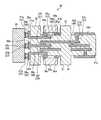
次に、内視鏡2の先端部6aの構成について詳細に説明する。図2は、内視鏡2の先端部6aの断面図である。図3は、図2に示す撮像ユニット30の斜視図である。図4は、図3の硬質基板31の斜視図である。図5は、図3の撮像ユニット30の断面図(1点鎖線を含む平面での断面図)である。なお、図2は、内視鏡2の後述するレンズユニット22の光軸O1および内視鏡軸O2に平行な面(レンズユニットの光軸O1および内視鏡軸O2を含む面)での断面図である。Next, the configuration of the
撮像装置は、レンズユニット22と、レンズユニット22の基端側に配置する撮像ユニット30とを有している。先端部本体41は、撮像装置を収容する内部空間を形成するための硬質部材で形成される。先端部本体41の外周部は、柔軟な被覆管42によって被覆されている。先端部本体41の先端面41aは斜面をなすように形成されている。 The image pickup apparatus includes a
レンズユニット22は、複数の対物レンズ22a、22bおよび22cと、対物レンズ22a〜22cを保持するレンズホルダ24とを有し、このレンズホルダ24が、先端部本体41内部に挿嵌固定されることによって、先端部本体41に固定されている。レンズユニット22の光軸O1は、内視鏡軸O2と所定の角度をなすように配置され、これにより被検体内を斜め方向から観察する。The
撮像ユニット30は、受光面である面f1で受光した光学像を、光電変換を行うことにより電気信号を生成する撮像素子を有し、裏面である面f2にセンサ電極27が形成された矩形状の半導体パッケージ25と、半導体パッケージ25を実装する半導体パッケージ実装領域31aと、電子部品50を実装する電子部品実装領域31bと、信号ケーブル48を実装するケーブル実装領域31cを有する硬質基板31と、を有する。半導体パッケージ25は、カバーガラス23を介して対物レンズ22cに接着固定されている。 The
半導体パッケージ25は、カバーガラス23を介して対物レンズ22cに接着固定されている。レンズユニット22が集光した光は、受光面であるf1面に入射する。半導体パッケージ25の面f2(裏面)には、センサ電極27が形成されている。半導体パッケージ25は、ウエハ状態の撮像素子チップに、配線、電極形成、樹脂封止、およびダイシングをして、最終的に撮像素子チップの大きさがそのまま半導体パッケージ25の大きさとなるCSP(Chip Size Package)であることが好ましい。 The
硬質基板31は、図3において矢印で示す方向(内視鏡軸O2と光軸O1を含む面に平行な方向)に、配線が形成された複数の基板が積層されてなる積層基板である(側面f4および側面f5に平行な基板が複数積層)。硬質基板31の内部には、積層される基板上の配線38を導通させるビア37が形成されている。硬質基板31を積層基板とすることにより、後述する電子部品実装領域31bの壁部33等の配置が容易となるが、硬質基板31は積層基板に限定されるものではない。積層される基板は、セラミックス基板、ガラエポ基板、ガラス基板、シリコン基板等を用いることができる。The
硬質基板31の半導体パッケージ実装領域31aは、レンズユニット22の光軸O1と直交する傾斜面f3に形成されている。傾斜面f3の傾きは、レンズユニット22が配置される先端部本体41の先端面41aの傾斜角度と同一である。半導体パッケージ実装領域31aには、半導体パッケージ25を接続する接続ランド35が形成され、半導体パッケージ25のセンサ電極27とはんだボール等の接合部材26を介して電気的、および機械的にそれぞれ接続されている。接合部材26は、はんだボールのほか、金属コアはんだボール、樹脂コアはんだボール、Auバンプ、等でもよい。接続ランド35は、スクリーン印刷、スパッタ、金属蒸着等により形成する。The semiconductor
電子部品実装領域31bは、半導体パッケージ実装領域31aが形成されている傾斜面f3と、傾斜面f3の水平方向の投影面と、傾斜面f3の鉛直方向の投影面とで囲まれる、硬質基板31の側面f4およびf5に配置されている。本実施の形態1では、傾斜面f3と、傾斜面f3の水平方向の投影面と、傾斜面f3の鉛直方向の投影面とで囲まれる、三角形状の側面に電子部品実装領域31bが配置されているが、少なくとも電子部品実装領域31bの一部がこの領域に配置されることにより、硬質基板31の内視鏡軸O2方向の長さを短くすることができ、内視鏡2の硬質部の短小化を図ることができる。The electronic
電子部品実装領域31bには、撮像素子の駆動回路を構成する電子部品50を接続する電子部品接続ランド36が形成され、電子部品50と半田等の接合部材を介して電気的、および機械的にそれぞれ接続されている。電子部品実装領域31bの三角形状の傾斜面f3側、および基端側のケーブル実装領域31c側には、壁部33が形成されている。壁部33の高さは、電子部品50を実装した際の電子部品の高さ以上となるように設計される。壁部33の高さを電子部品50の高さ以上とすることにより、周囲に配置された接着剤から電子部品50に加わる応力を緩和することができる。なお、本実施の形態1では、壁部33は三角形状の2辺に設けられるが、1辺または3辺でもよい。なお、電子部品実装領域31bには、撮像素子の駆動回路を構成する電子部品以外の電子部品が実装されてもよい。また、電子部品50は、硬質基板31の側面4fおよびf5の表面に実装されているが、傾斜面f3と、傾斜面f3の水平方向の投影面と、傾斜面f3の鉛直方向の投影面とで囲まれる、三角形状部分であれば、硬質基板31の内部に実装されていてもよい。 In the electronic
電子部品50を接続する電子部品接続ランド36は、電子部品が配線38およびビア37を介して接続される半導体パッケージ25のセンサ電極27の近傍に配置されることが好ましい。例えば、図5の側面f5に実装される電子部品50aは、電子部品接続ランド36a、ビア37a、配線38a、接続ランド35a、および接合部材26aを介してセンサ電極27aに接続されているが、配線38aの長さが短くなるように、すなわち、電子部品接続ランド36aを、センサ電極27aの近傍に配置する。これにより、撮像素子と電子部品50aとの距離を短くできるため、インピーダンスを小さくでき、撮像素子の安定的な駆動が可能となることで高画質の画像を得ることができる。側面f4に実装される電子部品50bについても同様に、配線38cの長さが短くなるように、電子部品接続ランド36cを、センサ電極27cの近傍に配置する。 The electronic
ケーブル実装領域31cは、電子部品実装領域31bの基端側に配置されている。ケーブル実装領域31cには、信号ケーブル48の芯線49が接続されるケーブル接続ランド34が形成され、芯線49と半田等の接合部材を介して電気的、および機械的にそれぞれ接続されている。 The
信号ケーブル48を接続するケーブル接続ランド34は、ケーブル実装領域31c内の、信号ケーブル48が接続される半導体パッケージ25のセンサ電極27bの近傍に配置されることが好ましい。例えば、図5の信号ケーブル48を接続するケーブル接続ランド34aは、ビア37d、ビア37e、配線38d、ビア37f、配線38f、接続ランド35b、および接続部材26bを介してセンサ電極27bに接続されているが、配線38d、38fの長さの和が短くなるように、ケーブル接続ランド34aをケーブル実装領域31c内に配置する。なお、図5では、ケーブル接続ランド34aは、センサ電極27bと異なる階層に設けられているが、センサ電極27bに接続するためのビアを減少させるために、ケーブル接続ランド34aを、センサ電極27bの近傍の階層の基板に形成してもよい。 The
信号ケーブル48の基端は、挿入部6の基端方向に延伸する。信号ケーブル束45は、挿入部6に挿通配置され、図1に示す操作部7およびユニバーサルコード8を介して、コネクタ8aおよび8bまで延設されている。 The base end of the
レンズユニット22の対物レンズ22a〜22cによって結像された光学像は、対物レンズ22a〜22cの結像位置に配設された撮像素子により画像信号に変換され、硬質基板31および信号ケーブル48を介して情報処理装置3に送信される。本実施の形態1では、硬質基板31に、先端部本体41の先端面41aの傾斜角度と同一の角度の傾斜面f3を設け、この傾斜面f3に半導体パッケージ25を実装する。硬質基板31はリジッドであるため、取扱いが容易であり、また、特殊な形状のプリズム等を使用することなく、歪み補正も不要であるため、コストの低減が可能となる。さらに、本実施の形態1では、硬質基板31の傾斜面f3と、傾斜面f3の水平方向の投影面と、傾斜面f3の鉛直方向の投影面とで囲まれる、三角形状の側面部分を電子部品実装領域31bとしているため、硬質基板31の内視鏡軸O2方向の長さを短くすることができ、小型化可能な斜視型内視鏡を得ることができる。The optical image formed by the
本実施の形態1では、硬質基板31の側面f4およびf5の両面に、電子部品実装領域31bおよびケーブル実装領域31cを形成しているが、一歩の側面のみに電子部品実装領域31bおよびケーブル実装領域31cを形成してもよい。図6は、本発明の実施の形態1の変形例にかかる撮像ユニット30Aの斜視図である。 In the first embodiment, the electronic
撮像ユニット30Aでは、硬質基板31Aの側面f4に電子部品実装領域31b、側面f5にケーブル実装領域31c−1、31c−2が形成されている。ケーブル実装領域31c−1とケーブル実装領域31c−2との間には段差S1が設けられている。電子部品実装領域31b、ケーブル実装領域31c−1、31c−2を、それぞれ1つの側面に配置することにより、電子部品50および信号ケーブル48の実装を、それぞれ1度で行うことができる。また、段差S1によりケーブル実装領域を31c−1と31c−2に分割することにより、多数の信号ケーブルを簡易に接続することができる。さらに、段差S1より硬質基板31Aは基端側の径が小さくなり、内視鏡の湾曲等により接続部へ応力が加えられた際にも、加えられた応力による影響を軽減することができる。なお、硬質基板31Aの側面f4には、側面f5と同様に段差S1が設けられているが、側面f4側には必ずしも段差S1を設ける必要はない。 In the
変形例1においても、傾斜面f3と、傾斜面f3の水平方向の投影面と、傾斜面f3の鉛直方向の投影面とで囲まれる、三角形状の側面に電子部品実装領域31bの一部を配置することにより、硬質基板31Aの内視鏡軸O2方向の長さを短くすることができ、内視鏡の硬質部の短小化を図ることができる。Also in the first modification, a part of the electronic
(実施の形態2)
図7は、本発明の実施の形態2にかかる撮像ユニット30Bの斜視図である。撮像ユニット30Bでは、電子部品実装領域31bの少なくとも一部は、傾斜面f3の鉛直方向の投影面であって、硬質基板31Bの底面f7に配置されている。(Embodiment 2)
FIG. 7 is a perspective view of the
硬質基板31Bは、図7において矢印で示す方向(内視鏡軸O2と光軸O1を含む面と直行する方向)に、配線が形成された複数の基板が積層されてなる積層基板である(上面f6面および底面f7面に平行な基板が複数積層)。The
硬質基板31Bの底面f7には、電子部品実装領域31b、ケーブル実装領域31c−1、31c−2、31c−3が形成されている。 An electronic
電子部品実装領域31bの傾斜面f3側には壁部33が配置され、電子部品実装領域31bとケーブル実装領域31c−1との間、ケーブル実装領域31c−1とケーブル実装領域31c−2との間、ケーブル実装領域31c−2とケーブル実装領域31c−3との間には、段差S1、S2、S3が設けられている。なお、電子部品実装領域31bとケーブル実装領域31c−1との間に設けられる段差S1は、必ずしも設ける必要はない。 A
電子部品実装領域31b、ケーブル実装領域31c−1、31c−2、31c−3を、底面f7に配置することにより、電子部品50および信号ケーブル48の実装を、それぞれ1度で行うことができる。また、段差S2、S3によりケーブル実装領域を31c−1、31c−2、31c−3に分割することにより、より多数の信号ケーブル48を簡易に接続することができる。なお、本実施の形態2では、ケーブル実装領域を3つに分割しているが、これに限定するものではなく、2つに分割してもよい。 By arranging the electronic
実施の形態2では、傾斜面f3の鉛直方向の投影面であって、硬質基板31Bの底面f7に電子部品実装領域31bの一部を配置することにより、硬質基板31Bの内視鏡軸O2方向の長さを短くすることができ、内視鏡の硬質部の短小化を図ることができる。In the second embodiment, it is a vertical projection surface of the inclined surface f3, and by arranging a part of the electronic
1 内視鏡システム
2 内視鏡
3 情報処理装置
4 光源装置
5 表示装置
6 挿入部
6a 先端部
6b 湾曲部
6c 可撓管部
7 操作部
7a 湾曲ノブ
7b 処置具挿入部
7c スイッチ部
8 ユニバーサルコード
8a、8b コネクタ
20 ライトガイドケーブル
21 照明レンズ
22 レンズユニット
23 カバーガラス
24 レンズホルダ
25 半導体パッケージ
26 接合部材
27 センサ電極
30、30A、30B 撮像ユニット
31 硬質基板
33 壁部
34 ケーブル接続ランド
35 接続ランド
36 電子部品接続ランド
37 ビア
38 配線
41 先端部本体
42 被覆管
45 信号ケーブル束
48 信号ケーブル
49 芯線
50 電子部品1
Claims (6)
Translated fromJapanese前記レンズユニットが形成する光学像を画像信号に変換する撮像素子を有し、裏面に端子が形成されている矩形状の半導体パッケージと、
前記半導体パッケージを実装する半導体パッケージ実装領域と、電子部品を実装する電子部品実装領域と、ケーブルを実装するケーブル実装領域を有する硬質基板と、を備え、
前記硬質基板は積層基板であって、積層方向は前記内視鏡軸と前記光軸を含む面に平行であり、
前記硬質基板の半導体パッケージ実装領域は、前記光軸と直交する傾斜面に形成され、
前記電子部品実装領域の少なくとも一部は、前記傾斜面と、前記傾斜面の水平方向の投影面と、前記傾斜面の鉛直方向の投影面とで囲まれる、前記硬質基板の三角形状の側面に配置されることを特徴とする斜視型内視鏡。In a perspective endoscope in which the endoscope axis, which is the longitudinal direction of the tip of the endoscope, and the optical axis of the lens unit, which is the observation direction, are arranged so as to have a predetermined tilt angle.
A rectangular semiconductor package having an image sensor that converts an optical image formed by the lens unit into an image signal and having terminals formed on the back surface thereof.
A semiconductor package mounting area for mounting the semiconductor package, an electronic component mounting area for mounting electronic components, and a hard substrate having a cable mounting area for mounting cables are provided.
The hard substrate is a laminated substrate, and the lamination direction is parallel to the surface including the endoscope axis and the optical axis.
The semiconductor package mounting region of the hard substrate is formed on an inclined surface orthogonal to the optical axis.
At least a part of the electronic component mounting region is formed on the triangular side surface of the hard substrate surrounded by the inclined surface, the horizontal projection surface of the inclined surface, and the vertical projection surface of the inclined surface. oblique endoscope anddisposed, wherein Rukoto.
Applications Claiming Priority (3)
| Application Number | Priority Date | Filing Date | Title |
|---|---|---|---|
| JP2018002611 | 2018-01-11 | ||
| JP2018002611 | 2018-01-11 | ||
| PCT/JP2018/035218WO2019138606A1 (en) | 2018-01-11 | 2018-09-21 | Oblique endoscope |
Publications (2)
| Publication Number | Publication Date |
|---|---|
| JPWO2019138606A1 JPWO2019138606A1 (en) | 2020-12-03 |
| JP6861851B2true JP6861851B2 (en) | 2021-04-21 |
Family
ID=67219572
Family Applications (1)
| Application Number | Title | Priority Date | Filing Date |
|---|---|---|---|
| JP2019564286AActiveJP6861851B2 (en) | 2018-01-11 | 2018-09-21 | Squint endoscope |
Country Status (3)
| Country | Link |
|---|---|
| US (1) | US11330972B2 (en) |
| JP (1) | JP6861851B2 (en) |
| WO (1) | WO2019138606A1 (en) |
Families Citing this family (8)
| Publication number | Priority date | Publication date | Assignee | Title |
|---|---|---|---|---|
| WO2018098465A1 (en) | 2016-11-28 | 2018-05-31 | Inventio, Inc. | Endoscope with separable, disposable shaft |
| JP7251940B2 (en)* | 2018-09-28 | 2023-04-04 | i-PRO株式会社 | strabismus endoscope |
| JP6792661B2 (en)* | 2019-03-27 | 2020-11-25 | Hoya株式会社 | Imaging module and endoscope |
| USD1018844S1 (en) | 2020-01-09 | 2024-03-19 | Adaptivendo Llc | Endoscope handle |
| USD1051380S1 (en) | 2020-11-17 | 2024-11-12 | Adaptivendo Llc | Endoscope handle |
| USD1070082S1 (en) | 2021-04-29 | 2025-04-08 | Adaptivendo Llc | Endoscope handle |
| USD1031035S1 (en) | 2021-04-29 | 2024-06-11 | Adaptivendo Llc | Endoscope handle |
| USD1066659S1 (en) | 2021-09-24 | 2025-03-11 | Adaptivendo Llc | Endoscope handle |
Family Cites Families (6)
| Publication number | Priority date | Publication date | Assignee | Title |
|---|---|---|---|---|
| US4918521A (en)* | 1987-01-20 | 1990-04-17 | Olympus Optical Co., Ltd. | Solid state imaging apparatus |
| JPH09122070A (en) | 1995-10-30 | 1997-05-13 | Fuji Photo Optical Co Ltd | Skew type electronic endoscope |
| JPH1189794A (en)* | 1997-09-24 | 1999-04-06 | Olympus Optical Co Ltd | Electronic endoscope |
| JP3486804B2 (en)* | 1998-03-30 | 2004-01-13 | 富士写真光機株式会社 | Tip structure of insertion section for oblique endoscope |
| US6494739B1 (en)* | 2001-02-07 | 2002-12-17 | Welch Allyn, Inc. | Miniature connector with improved strain relief for an imager assembly |
| JP4789487B2 (en) | 2005-03-07 | 2011-10-12 | オリンパスメディカルシステムズ株式会社 | Endoscope |
- 2018
- 2018-09-21WOPCT/JP2018/035218patent/WO2019138606A1/ennot_activeCeased
- 2018-09-21JPJP2019564286Apatent/JP6861851B2/enactiveActive
- 2020
- 2020-07-09USUS16/924,631patent/US11330972B2/enactiveActive
Also Published As
| Publication number | Publication date |
|---|---|
| US20200337538A1 (en) | 2020-10-29 |
| WO2019138606A1 (en) | 2019-07-18 |
| JPWO2019138606A1 (en) | 2020-12-03 |
| US11330972B2 (en) | 2022-05-17 |
Similar Documents
| Publication | Publication Date | Title |
|---|---|---|
| JP6861851B2 (en) | Squint endoscope | |
| US9462933B2 (en) | Image pickup unit for endoscope | |
| CN112135557B (en) | Imaging unit and strabismus endoscope | |
| JP5964003B1 (en) | Imaging unit, imaging module, and endoscope system | |
| JP6307697B1 (en) | Electronic circuit unit, imaging unit, imaging module, and endoscope | |
| JP6293391B1 (en) | Imaging unit and endoscope | |
| WO2017130886A1 (en) | Imaging unit, imaging module, and endoscope | |
| JP6529703B2 (en) | Imaging unit and endoscope | |
| US10321805B2 (en) | Imaging unit, imaging module, and endoscope | |
| JP2019195382A (en) | Imaging unit and oblique-viewing type or side-viewing type endoscope | |
| JP6324644B1 (en) | Imaging unit and endoscope | |
| WO2019193911A1 (en) | Imaging unit and endoscope | |
| WO2018079328A1 (en) | Image capture unit and endoscope system | |
| JP7138520B2 (en) | Imaging unit and endoscope | |
| JP2022142206A (en) | Imaging module | |
| JP6165402B1 (en) | Imaging unit, imaging module, and endoscope | |
| JP6297240B1 (en) | Electronic circuit unit, imaging unit and endoscope | |
| WO2019097588A1 (en) | Cable connection structure, imaging device, and endoscope | |
| US10568498B2 (en) | Imaging unit and endoscope | |
| JP6165395B1 (en) | Imaging unit, imaging module, and endoscope | |
| US20210096354A1 (en) | Image pickup apparatus, endoscope apparatus, and method of electrical connection to image pickup module in image pickup apparatus |
Legal Events
| Date | Code | Title | Description |
|---|---|---|---|
| A521 | Request for written amendment filed | Free format text:JAPANESE INTERMEDIATE CODE: A523 Effective date:20200521 | |
| A621 | Written request for application examination | Free format text:JAPANESE INTERMEDIATE CODE: A621 Effective date:20200521 | |
| TRDD | Decision of grant or rejection written | ||
| A01 | Written decision to grant a patent or to grant a registration (utility model) | Free format text:JAPANESE INTERMEDIATE CODE: A01 Effective date:20210309 | |
| A61 | First payment of annual fees (during grant procedure) | Free format text:JAPANESE INTERMEDIATE CODE: A61 Effective date:20210330 | |
| R151 | Written notification of patent or utility model registration | Ref document number:6861851 Country of ref document:JP Free format text:JAPANESE INTERMEDIATE CODE: R151 | |
| R250 | Receipt of annual fees | Free format text:JAPANESE INTERMEDIATE CODE: R250 | |
| R250 | Receipt of annual fees | Free format text:JAPANESE INTERMEDIATE CODE: R250 |