JP6850821B6 - Touch screen sensor - Google Patents
Touch screen sensorDownload PDFInfo
- Publication number
- JP6850821B6 JP6850821B6JP2019048195AJP2019048195AJP6850821B6JP 6850821 B6JP6850821 B6JP 6850821B6JP 2019048195 AJP2019048195 AJP 2019048195AJP 2019048195 AJP2019048195 AJP 2019048195AJP 6850821 B6JP6850821 B6JP 6850821B6
- Authority
- JP
- Japan
- Prior art keywords
- conductive
- area
- micrometers
- micropattern
- sheet resistance
- Prior art date
- Legal status (The legal status is an assumption and is not a legal conclusion. Google has not performed a legal analysis and makes no representation as to the accuracy of the status listed.)
- Active
Links
Images


Classifications
- G—PHYSICS
- G06—COMPUTING OR CALCULATING; COUNTING
- G06F—ELECTRIC DIGITAL DATA PROCESSING
- G06F3/00—Input arrangements for transferring data to be processed into a form capable of being handled by the computer; Output arrangements for transferring data from processing unit to output unit, e.g. interface arrangements
- G06F3/01—Input arrangements or combined input and output arrangements for interaction between user and computer
- G06F3/03—Arrangements for converting the position or the displacement of a member into a coded form
- G06F3/041—Digitisers, e.g. for touch screens or touch pads, characterised by the transducing means
- G06F3/044—Digitisers, e.g. for touch screens or touch pads, characterised by the transducing means by capacitive means
- G06F3/0446—Digitisers, e.g. for touch screens or touch pads, characterised by the transducing means by capacitive means using a grid-like structure of electrodes in at least two directions, e.g. using row and column electrodes
- B—PERFORMING OPERATIONS; TRANSPORTING
- B82—NANOTECHNOLOGY
- B82Y—SPECIFIC USES OR APPLICATIONS OF NANOSTRUCTURES; MEASUREMENT OR ANALYSIS OF NANOSTRUCTURES; MANUFACTURE OR TREATMENT OF NANOSTRUCTURES
- B82Y10/00—Nanotechnology for information processing, storage or transmission, e.g. quantum computing or single electron logic
- B—PERFORMING OPERATIONS; TRANSPORTING
- B82—NANOTECHNOLOGY
- B82Y—SPECIFIC USES OR APPLICATIONS OF NANOSTRUCTURES; MEASUREMENT OR ANALYSIS OF NANOSTRUCTURES; MANUFACTURE OR TREATMENT OF NANOSTRUCTURES
- B82Y40/00—Manufacture or treatment of nanostructures
- G—PHYSICS
- G03—PHOTOGRAPHY; CINEMATOGRAPHY; ANALOGOUS TECHNIQUES USING WAVES OTHER THAN OPTICAL WAVES; ELECTROGRAPHY; HOLOGRAPHY
- G03F—PHOTOMECHANICAL PRODUCTION OF TEXTURED OR PATTERNED SURFACES, e.g. FOR PRINTING, FOR PROCESSING OF SEMICONDUCTOR DEVICES; MATERIALS THEREFOR; ORIGINALS THEREFOR; APPARATUS SPECIALLY ADAPTED THEREFOR
- G03F7/00—Photomechanical, e.g. photolithographic, production of textured or patterned surfaces, e.g. printing surfaces; Materials therefor, e.g. comprising photoresists; Apparatus specially adapted therefor
- G03F7/0002—Lithographic processes using patterning methods other than those involving the exposure to radiation, e.g. by stamping
- G—PHYSICS
- G06—COMPUTING OR CALCULATING; COUNTING
- G06F—ELECTRIC DIGITAL DATA PROCESSING
- G06F3/00—Input arrangements for transferring data to be processed into a form capable of being handled by the computer; Output arrangements for transferring data from processing unit to output unit, e.g. interface arrangements
- G06F3/01—Input arrangements or combined input and output arrangements for interaction between user and computer
- G06F3/03—Arrangements for converting the position or the displacement of a member into a coded form
- G06F3/041—Digitisers, e.g. for touch screens or touch pads, characterised by the transducing means
- G06F3/0412—Digitisers structurally integrated in a display
- G—PHYSICS
- G06—COMPUTING OR CALCULATING; COUNTING
- G06F—ELECTRIC DIGITAL DATA PROCESSING
- G06F3/00—Input arrangements for transferring data to be processed into a form capable of being handled by the computer; Output arrangements for transferring data from processing unit to output unit, e.g. interface arrangements
- G06F3/01—Input arrangements or combined input and output arrangements for interaction between user and computer
- G06F3/03—Arrangements for converting the position or the displacement of a member into a coded form
- G06F3/041—Digitisers, e.g. for touch screens or touch pads, characterised by the transducing means
- G06F3/044—Digitisers, e.g. for touch screens or touch pads, characterised by the transducing means by capacitive means
- G06F3/0445—Digitisers, e.g. for touch screens or touch pads, characterised by the transducing means by capacitive means using two or more layers of sensing electrodes, e.g. using two layers of electrodes separated by a dielectric layer
- G—PHYSICS
- G06—COMPUTING OR CALCULATING; COUNTING
- G06F—ELECTRIC DIGITAL DATA PROCESSING
- G06F3/00—Input arrangements for transferring data to be processed into a form capable of being handled by the computer; Output arrangements for transferring data from processing unit to output unit, e.g. interface arrangements
- G06F3/01—Input arrangements or combined input and output arrangements for interaction between user and computer
- G06F3/03—Arrangements for converting the position or the displacement of a member into a coded form
- G06F3/041—Digitisers, e.g. for touch screens or touch pads, characterised by the transducing means
- G06F3/045—Digitisers, e.g. for touch screens or touch pads, characterised by the transducing means using resistive elements, e.g. a single continuous surface or two parallel surfaces put in contact
- H—ELECTRICITY
- H01—ELECTRIC ELEMENTS
- H01B—CABLES; CONDUCTORS; INSULATORS; SELECTION OF MATERIALS FOR THEIR CONDUCTIVE, INSULATING OR DIELECTRIC PROPERTIES
- H01B5/00—Non-insulated conductors or conductive bodies characterised by their form
- H01B5/14—Non-insulated conductors or conductive bodies characterised by their form comprising conductive layers or films on insulating-supports
- H—ELECTRICITY
- H05—ELECTRIC TECHNIQUES NOT OTHERWISE PROVIDED FOR
- H05K—PRINTED CIRCUITS; CASINGS OR CONSTRUCTIONAL DETAILS OF ELECTRIC APPARATUS; MANUFACTURE OF ASSEMBLAGES OF ELECTRICAL COMPONENTS
- H05K3/00—Apparatus or processes for manufacturing printed circuits
- H05K3/0073—Masks not provided for in groups H05K3/02 - H05K3/46, e.g. for photomechanical production of patterned surfaces
- H05K3/0079—Masks not provided for in groups H05K3/02 - H05K3/46, e.g. for photomechanical production of patterned surfaces characterised by the method of application or removal of the mask
- H—ELECTRICITY
- H05—ELECTRIC TECHNIQUES NOT OTHERWISE PROVIDED FOR
- H05K—PRINTED CIRCUITS; CASINGS OR CONSTRUCTIONAL DETAILS OF ELECTRIC APPARATUS; MANUFACTURE OF ASSEMBLAGES OF ELECTRICAL COMPONENTS
- H05K3/00—Apparatus or processes for manufacturing printed circuits
- H05K3/02—Apparatus or processes for manufacturing printed circuits in which the conductive material is applied to the surface of the insulating support and is thereafter removed from such areas of the surface which are not intended for current conducting or shielding
- H05K3/06—Apparatus or processes for manufacturing printed circuits in which the conductive material is applied to the surface of the insulating support and is thereafter removed from such areas of the surface which are not intended for current conducting or shielding the conductive material being removed chemically or electrolytically, e.g. by photo-etch process
- H05K3/061—Etching masks
- G—PHYSICS
- G06—COMPUTING OR CALCULATING; COUNTING
- G06F—ELECTRIC DIGITAL DATA PROCESSING
- G06F2203/00—Indexing scheme relating to G06F3/00 - G06F3/048
- G06F2203/041—Indexing scheme relating to G06F3/041 - G06F3/045
- G06F2203/04103—Manufacturing, i.e. details related to manufacturing processes specially suited for touch sensitive devices
- G—PHYSICS
- G06—COMPUTING OR CALCULATING; COUNTING
- G06F—ELECTRIC DIGITAL DATA PROCESSING
- G06F2203/00—Indexing scheme relating to G06F3/00 - G06F3/048
- G06F2203/041—Indexing scheme relating to G06F3/041 - G06F3/045
- G06F2203/04112—Electrode mesh in capacitive digitiser: electrode for touch sensing is formed of a mesh of very fine, normally metallic, interconnected lines that are almost invisible to see. This provides a quite large but transparent electrode surface, without need for ITO or similar transparent conductive material
Landscapes
- Engineering & Computer Science (AREA)
- Theoretical Computer Science (AREA)
- General Engineering & Computer Science (AREA)
- Physics & Mathematics (AREA)
- General Physics & Mathematics (AREA)
- Human Computer Interaction (AREA)
- Nanotechnology (AREA)
- Chemical & Material Sciences (AREA)
- Manufacturing & Machinery (AREA)
- Microelectronics & Electronic Packaging (AREA)
- Crystallography & Structural Chemistry (AREA)
- Mathematical Physics (AREA)
- Condensed Matter Physics & Semiconductors (AREA)
- Position Input By Displaying (AREA)
- Laminated Bodies (AREA)
- Structure Of Printed Boards (AREA)
- Manufacturing Of Printed Wiring (AREA)
- Non-Insulated Conductors (AREA)
Description
Translated fromJapanese (関連出願の相互参照)
本願は、2008年2月28日に出願された米国特許仮出願第61/032,269号(その開示は参照によりその全体が本明細書に組み込まれる)、2008年2月28日に出願された同第61/032,273号(その開示は参照によりその全体が本明細書に組み込まれる)、2008年8月1日に出願された同第61/085,496号(その開示は参照によりその全体が本明細書に組み込まれる)、及び2008年8月1日に出願された同第61/085,764号(その開示は参照によりその全体が本明細書に組み込まれる)の利益を請求する。(Cross-reference of related applications)
This application is filed on February 28, 2008, US Patent Provisional Application No. 61 / 032,269, filed February 28, 2008 (the disclosure of which is incorporated herein by reference in its entirety). No. 61 / 032,273 (the disclosure of which is incorporated herein by reference in its entirety) and No. 61 / 085,496, which was filed on August 1, 2008 (the disclosure of which is by reference). Incorporate in its entirety herein) and claims the benefits of No. 61 / 085,764 filed on August 1, 2008 (the disclosure of which is incorporated herein by reference in its entirety). To do.
タッチスクリーンセンサは、タッチスクリーンディスプレイの表面に適用された物体(例えば、指、又はスタイラス)の位置、又はタッチスクリーンディスプレイの表面の付近に位置付けられた物体の位置を検出する。これらのセンサは、ディスプレイの表面に沿った、例えば、平坦な矩形のディスプレイの平面にある物体の位置を検出する。タッチスクリーンセンサの例としては、静電容量センサ、抵抗センサ、及び投影型静電容量センサが挙げられる。このようなセンサとしては、ディスプレイに重ねる透明導電性素子が挙げられる。この素子は、ディスプレイの付近の、又はこれと接触する物体の位置を決定するために、素子を探査する電気信号を使用する、電子的構成要素と組み合わされる。 The touch screen sensor detects the position of an object (eg, a finger, or stylus) applied to the surface of the touch screen display, or the position of an object located near the surface of the touch screen display. These sensors detect the position of an object along the surface of the display, eg, in the plane of a flat rectangular display. Examples of touch screen sensors include capacitance sensors, resistance sensors, and projected capacitance sensors. Examples of such a sensor include a transparent conductive element that is superimposed on the display. The device is combined with an electronic component that uses an electrical signal to explore the device to determine the position of an object near or in contact with the display.
タッチスクリーンセンサの分野では、光学品質、又はディスプレイの特性を損なうことなく、透明タッチスクリーンセンサの電気的特性の制御を改善する必要性が存在する。典型的なタッチスクリーンセンサの透明導電性区域は、透明導電性酸化物(TCO)、例えば、酸化インジウムスズ(ITO)の連続的なコーティングを含み、コーティングは、電圧源との接触位置、及び区域の全体形状に基づく電位勾配を呈する。この事実は、可能なタッチセンサの設計及びセンサの性能に対する制約へと繋がり、電位勾配を修正するための高価な信号処理電子機器又は追加的な電極の配置などの手段を必要とする。したがって、前述の要因とは別の、電位勾配の制御を提供する、透明導電性素子の必要性が存在する。 In the field of touch screen sensors, there is a need to improve the control of the electrical properties of transparent touch screen sensors without compromising optical quality or display properties. The transparent conductive area of a typical touch screen sensor comprises a continuous coating of transparent conductive oxide (TCO), such as indium tin oxide (ITO), the coating being the contact position with the voltage source and the area. It exhibits a potential gradient based on the overall shape of. This fact leads to constraints on possible touch sensor designs and sensor performance, requiring means such as expensive signal processing electronics or the placement of additional electrodes to correct the potential gradient. Therefore, there is a need for transparent conductive devices that provide control of the potential gradient, which is different from the factors described above.
導電性素子の設計における順応性に関する、タッチスクリーンセンサの分野における追加的な必要性が存在する。パターン化された透明導電性酸化物(TCO)、例えば、酸化インジウムスズ(ITO)を使用するタッチスクリーンセンサの作製は、多くの場合、導電体の設計に制限を課す。この制限は、単一の等方性シート抵抗値を有する透明シート導電体の導電性素子全てをパターン化することによって生じる制約に関する。 There is an additional need in the field of touch screen sensors for adaptability in the design of conductive devices. Fabrication of touch screen sensors using patterned transparent conductive oxides (TCOs), such as indium tin oxide (ITO), often imposes restrictions on conductor design. This limitation relates to the constraint created by patterning all the conductive elements of a transparent sheet conductor having a single isotropic sheet resistance value.
一態様では、本開示は、透明基材と、高い光学品質を達成するための特定のパターン形状で微小パターン化された導電体(典型的には、金属)と、を有する、タッチスクリーンセンサに関する。一般的に、光学品質は、導電体がタッチスクリーンセンサに組み立てられた際に、それを裸眼で観察して判断される可視光透過性、ヘイズ、及び導電体可視性という点において表現され得る。微小パターン化された導電体の形状は、微小パターンに使用される導電体配線(場合によって「線」と称される)の幅、線の密度、線の密度の均一性が挙げられるがこれらに限定されないパラメータによって規定され得る。 In one aspect, the present disclosure relates to a touch screen sensor having a transparent substrate and a conductor (typically a metal) micropatterned with a particular pattern shape to achieve high optical quality. .. In general, optical quality can be expressed in terms of visible light transmission, haze, and conductor visibility, which are determined by observing the conductor as assembled into a touch screen sensor with the naked eye. The shape of the micropatterned conductor includes the width of the conductor wiring (sometimes referred to as the "line") used for the micropattern, the line density, and the uniformity of the line density. It can be specified by unrestricted parameters.
良好な光学品質を有するタッチスクリーンセンサの第1実施形態では、タッチスクリーンセンサは、可視光透明基材と、可視光透明基材の上又は中に配置される導電性微小パターンと、を含む。微小パターンは、マイクロメートルの単位で約[X+0.5]の導電体配線幅、及び約[95−X]%〜99.5%の開口率(0≦X≦4.5)を有する。別の実施形態では、タッチスクリーンは、約[98.5−(2.5X÷3.5)]%〜[99.5−(X÷3.5)]%(0≦X≦3.5)の開口率を有する。別の実施形態では、タッチスクリーンセンサは、10%未満、好ましくは5%未満のヘイズ値、及び75%超、好ましくは85%超の可視光透過率を有する。別の実施形態では、タッチスクリーンセンサの導電体配線幅は、約6マイクロメートル未満であり、約300マイクロメートル未満のピッチを有する。別の実施形態では、タッチスクリーンセンサの導電体配線は、約500ナノメートル未満の厚さを有する。別の実施形態では、ピッチは約1mm〜4mmであり、導電体の幅は3〜10マイクロメートルである。 In a first embodiment of a touch screen sensor having good optical quality, the touch screen sensor comprises a visible light transparent substrate and a conductive micropattern placed on or in a visible light transparent substrate. The micropattern has a conductor wiring width of about [X + 0.5] in micrometers and an aperture ratio (0 ≦ X ≦ 4.5) of about [95-X]% to 99.5%. In another embodiment, the touch screen is about [98.5- (2.5X ÷ 3.5)]% to [99.5- (X ÷ 3.5)]% (0 ≦ X ≦ 3.5). ) Has an aperture ratio. In another embodiment, the touch screen sensor has a haze value of less than 10%, preferably less than 5%, and a visible light transmittance of greater than 75%, preferably greater than 85%. In another embodiment, the conductor wiring width of the touch screen sensor is less than about 6 micrometers and has a pitch of less than about 300 micrometers. In another embodiment, the conductor wiring of the touch screen sensor has a thickness of less than about 500 nanometers. In another embodiment, the pitch is about 1 mm to 4 mm and the width of the conductor is 3 to 10 micrometers.
別の態様では、本開示は、変化するシート抵抗を有するタッチスクリーンセンサに関する。 In another aspect, the present disclosure relates to a touch screen sensor with varying sheet resistance.
変化するシート抵抗を有するタッチスクリーンセンサの第1実施形態では、センサは、可視光透明基材と、可視光透明基材の上又は中に配置される導電性微小パターンと、を含む。微小パターンは、接触感知領域内の第1区域微小パターン、及び第2区域微小パターンを含む。第1区域微小パターンは、第1の方向において第1シート抵抗値を有し、可視光透明であり、少なくとも90%の開口を有する。第2区域微小パターンは、第1の方向において、第2シート抵抗値を有する。第1シート抵抗値は、第2シート抵抗値とは異なる。 In a first embodiment of a touch screen sensor with varying sheet resistance, the sensor comprises a visible light transparent substrate and a conductive micropattern placed on or in the visible light transparent substrate. The micro pattern includes a first zone micro pattern and a second zone micro pattern within the contact sensing region. The first area micropattern has a first sheet resistance value in the first direction, is visible light transparent, and has an aperture of at least 90%. The second zone micropattern has a second sheet resistance value in the first direction. The first sheet resistance value is different from the second sheet resistance value.
変化するシート抵抗を有するタッチスクリーンセンサの別の実施形態では、センサは、可視光透明基材と、可視光透明基材の上又は中に配置される導電性微小パターンと、を含む。微小パターンは、接触感知領域内の第1区域微小パターンを含み、第1区域微小パターンは、異方性第1シート抵抗を有し、可視光透明であり、少なくとも90%の開口を有する。 In another embodiment of a touch screen sensor with varying sheet resistance, the sensor comprises a visible light transparent substrate and a conductive micropattern placed on or in a visible light transparent substrate. The micropattern includes a first segment micropattern within the contact sensing region, the first segment micropattern has anisotropic first sheet resistance, is visible light transparent, and has an aperture of at least 90%.
変化するシート抵抗を有するタッチスクリーンセンサの別の実施形態では、センサは、可視光透明基材と、可視光透明基材の上又は中に配置される導電性微小パターンと、を含む。微小パターンは、接触感知領域内の第1区域微小パターン、及び第2区域微小パターンを含む。導電性微小パターンは、500ナノメートル未満の厚さ、及び0.5〜5マイクロメートルの幅を有する金属の線形導電性構造を有する。第1区域微小パターンは、第1の方向において5〜500Ω/スクエアの第1シート抵抗値を有し、可視光透明であり、95%〜99.5%の開口(又は別の実施形態では、更に99.9%の開口、若しくは更に99.95%の開口)を有する。第2区域微小パターンは、第1の方向において第2シート抵抗値を有する。第1シート抵抗値は、第2シート抵抗値とは異なる。 In another embodiment of a touch screen sensor with varying sheet resistance, the sensor comprises a visible light transparent substrate and a conductive micropattern placed on or in a visible light transparent substrate. The micro pattern includes a first zone micro pattern and a second zone micro pattern within the contact sensing region. The conductive micropattern has a linear conductive structure of metal with a thickness of less than 500 nanometers and a width of 0.5-5 micrometers. The first area micropattern has a first sheet resistance value of 5 to 500 Ω / square in the first direction, is visible light transparent, and has an aperture of 95% to 99.5% (or, in another embodiment,). It has an additional 99.9% opening, or an additional 99.95% opening). The second zone micropattern has a second sheet resistance value in the first direction. The first sheet resistance value is different from the second sheet resistance value.
変化するシート抵抗を有するタッチスクリーンセンサの更なる実施形態では、センサは、可視光透明基材と、可視光透明基材の上又は中に配置される導電性微小パターンと、を含む。微小パターンは、接触感知領域内に第1区域微小パターンを含む。導電性微小パターンは、500ナノメートル未満の厚さ、及び0.5〜5マイクロメートルの幅を有する、金属の線形導電性構造を含む。第1区域微小パターンは、直交方向において、少なくとも1.5倍のシート抵抗値の差を有する異方性第1シート抵抗を有し、可視光透明であり、95%〜99.5%の開口を有する。 In a further embodiment of a touch screen sensor with varying sheet resistance, the sensor comprises a visible light transparent substrate and a conductive micropattern placed on or in the visible light transparent substrate. The micro pattern includes a first zone micro pattern within the contact sensing region. Conductive micropatterns include linear conductive structures of metals with a thickness of less than 500 nanometers and a width of 0.5-5 micrometers. The first zone micropattern has an anisotropic first sheet resistance with a difference of at least 1.5 times the sheet resistance value in the orthogonal direction, is visible light transparent, and has an aperture of 95% to 99.5%. Has.
更なる実施形態では、可視光透明基材と、可視光透明基材の上又は中に配置される接触感知導電性微小パターンと、を含み、微小パターンは、約1〜10マイクロメートルの幅を有する導電配線を含む、タッチスクリーンセンサが記載される。 In a further embodiment, it comprises a visible light transparent substrate and a contact-sensitive conductive micropattern disposed on or in a visible light transparent substrate, the micropattern having a width of about 1-10 micrometer. Described is a touch screen sensor that includes conductive wiring having.
添付の図面と共に本発明の様々な実施形態の以下の詳細な説明を検討することで、本発明はより完全に理解され得る。
図面は、必ずしも縮尺に従っていない。図面で用いられる同様の番号は、同様の構成要素を指す。しかしながら、所定の図中の構成要素を指す数字の使用は、同じ数字を付けられた別の図中の構成要素を限定することを意図するものではないことが理解されよう。 Drawings do not necessarily follow scale. Similar numbers used in the drawings refer to similar components. However, it will be understood that the use of numbers to refer to a component in a given figure is not intended to limit the component in another figure with the same number.
以下の説明において、本明細書の一部を構成し複数の特定の実施形態が例として示される添付の一連の図面を参照する。本発明の範囲又は趣旨を逸脱せずに、その他の実施形態が考えられ、実施され得ることを理解すべきである。したがって、以下の「発明を実施するための形態」は、限定する意味で理解すべきではない。 In the following description, reference is made to a series of accompanying drawings that form part of the specification and show, for example, a plurality of specific embodiments. It should be understood that other embodiments may be conceivable and implemented without departing from the scope or gist of the present invention. Therefore, the following "forms for carrying out the invention" should not be understood in a limited sense.
本発明で使用する全ての科学用語及び専門用語は、特に指示がない限り、当該技術分野において一般的に使用される意味を有する。本明細書にて提供される定義は、本明細書でしばしば使用される特定の用語の理解を促進しようとするものであり、本開示の範囲を限定するものではない。 All scientific and technical terms used in the present invention have meanings commonly used in the art, unless otherwise indicated. The definitions provided herein are intended to facilitate understanding of certain terms often used herein and are not intended to limit the scope of this disclosure.
他に指示がない限り、本明細書及び特許請求の範囲で使用される形状寸法、量、及び物理特性を表わす数字は全て、どの場合においても用語「約」によって修飾されるものとして理解されるべきである。それゆえに、そうでないことが示されない限り、前述の明細書及び添付の特許請求の範囲で示される数値パラメータは、当業者が本明細書で開示される教示内容を用いて、目標対象とする所望の特性に応じて、変化し得る近似値である。 Unless otherwise indicated, all numbers representing shape dimensions, quantities, and physical characteristics used herein and in the claims are to be understood as being modified by the term "about" in all cases. Should be. Therefore, unless otherwise indicated, the numerical parameters shown in the specification and the appended claims are desired to be targeted by those skilled in the art using the teachings disclosed herein. It is an approximate value that can be changed according to the characteristics of.
端点による数値範囲の列挙には、その範囲内の全ての数(例えば1〜5には、1、1.5、2、2.75、3、3.80、4、及び5が含まれる)、及びその範囲内の任意の範囲が含まれる。 The enumeration of numerical ranges by endpoints includes all numbers within that range (eg, 1-5 includes 1, 1.5, 2, 2.75, 3, 3.80, 4, and 5). , And any range within that range.
本明細書及び添付の特許請求の範囲において使用されるとき、単数形「a(1つの)」、「an(1つの)」及び「the(その)」は、その文脈が特に明確に指示しない限り、複数の指示対象を有する実施形態を包含する。本明細書及び添付の特許請求の範囲において使用されるとき、用語「又は」は、その文脈が特に明確に指示しない限り、一般的に「及び/又は」を包含する意味で用いられる。 As used herein and in the appended claims, the singular forms "a", "an" and "the" do not specifically indicate in their context. As long as it includes an embodiment having a plurality of referents. As used herein and in the appended claims, the term "or" is generally used to include "and / or" unless the context specifically dictates otherwise.
本明細書で使用するとき、「可視光透明」とは、少なくとも1つの偏光状態の可視光に対して、少なくとも60パーセント透過性である透過率の水準を指し、ここで透過率パーセントは、入射光、任意により偏光の強度に正規化される。入射光の少なくとも60%を透過する物品が、局部的に光を透過率80パーセント未満(例えば、0%)に遮蔽する微細構造(例えば、最小寸法、例えば0.5〜10マイクロメートル、又は1〜5マイクロメートルの幅の点、正方形、又は線)を含むのは、可視光線透明性の意味の範囲内であるが、このような場合、微細構造を含み、微細構造の最小寸法の1000倍の幅である、およそ等軸の面積に関して、平均透過率は60パーセントを超える。 As used herein, "visible light transparent" refers to a level of transmittance that is at least 60% transparent to visible light in at least one polarized state, where the percent transmittance is incident. Light, optionally normalized to the intensity of polarization. An article that transmits at least 60% of the incident light locally shields the light to less than 80% (eg 0%) microstructure (eg, minimum dimensions, eg 0.5-10 micrometer, or 1). Includes points, squares, or lines with a width of ~ 5 micrometer) within the meaning of visible light transparency, but in such cases, includes microstructures, 1000 times the minimum dimensions of microstructures. With respect to the approximately equiaxed area, which is the width of, the average transmittance exceeds 60%.
本開示は、内部に含まれる導電体微小パターンの設計を通じて設計される、電気的及び光学的特性を有するタッチスクリーンセンサに関する。本明細書において記載される導電体微小パターンを組み込むことにより、タッチスクリーンセンサにもたらされるいくつかの利点が存在する。いくつかの実施形態では、透明導電性区域内の透明導電特性は、使用中の接触感知区域内の電位勾配を制御するように設計される。これは、信号処理電子機器の単純化、及びいくつかの接触スクリーンセンサの種類においては、本来ならば電位勾配(電場)線形化に必要とされる追加的な導電体パターンの設計の単純化(又はその必要性の排除)に繋がる。いくつかの実施形態では、本明細書において記載されるタッチスクリーンセンサの電気的特性は、透明センサ要素に沿って、制御された電位勾配を生成するように設計される。例えば、電気的特性は、透明導電性区域内の特定の方向に沿った線形電位勾配を生成するように設計され、その全体的な形状は通常、標準的な透明導電体材料(例えば、連続的ITOコーティング)が使用された場合、非線形の勾配に繋がる。いくつかの実施形態では、電気的特性は、同じ形状であるが標準的な透明導電体材料(例えば、連続的ITOコーティング)からなる透明導電性区域内に存在するものよりも高い、透明導電性区域の電位勾配の非線形性の水準を生じるように設計される。より詳細には、微小パターン化された導電体の形態の、隣接する透明シート導電体を含み、感知領域の角部への電気的接続が作られる矩形の静電容量タッチスクリーンにおいては、感知領域にわたる電位勾配の垂直方向及び水平方向の線形性(電界の均一性)が、シート抵抗値の領域分布及び異方性を、場をより均一に分配するような方法で設計することによって改善され得る。他の実施形態では、センサは、同じ厚さ(即ち、同じ高さ)の同じ導電体材料からなるが、微小パターン化による異なる有効シート抵抗値を有する導電体素子を含む。例えば、いくつかの実施形態では、同じ厚さ(即ち、高さ)の同じ導電体材料が使用されて、透明導電性区域の第1の水準のシート抵抗に繋がる第1の微小パターン形状を画定する導電配線、及び第2の透明導電性区域の第2の水準のシート抵抗に繋がる第2の微小パターン形状を画定する導電配線を生成する。本開示はまた、いくつかの実施形態、例えば、微小パターン化された金属導電体に基づく実施形態において、例えば、インジウムなどの希元素を避けることによって、透明ディスプレイセンサの製造における、改善された効率性及び資源利用を可能にする。 The present disclosure relates to touch screen sensors having electrical and optical properties designed through the design of conductor micropatterns contained therein. There are several advantages to the touch screen sensor by incorporating the conductor micropatterns described herein. In some embodiments, the transparent conductive properties within the transparent conductive area are designed to control the potential gradient within the contact sensing area in use. This simplifies signal processing electronics and, in some contact screen sensor types, simplification of the design of additional conductor patterns that would otherwise be required for potential gradient (electric field) linearization. Or eliminate the need for it). In some embodiments, the electrical properties of the touch screen sensors described herein are designed to generate a controlled potential gradient along the transparent sensor elements. For example, the electrical properties are designed to generate a linear potential gradient along a particular direction within the transparent conductive area, the overall shape of which is usually a standard transparent conductor material (eg, continuous). If an ITO coating) is used, it leads to a non-linear gradient. In some embodiments, the electrical properties are higher than those present in a transparent conductive area of the same shape but made of a standard transparent conductive material (eg, a continuous ITO coating). Designed to produce a level of non-linearity of the potential gradient of the region. More specifically, in a rectangular capacitive touch screen that includes adjacent transparent sheet conductors in the form of micropatterned conductors and that makes electrical connections to the corners of the sensing area, the sensing area. The vertical and horizontal linearity (electric field uniformity) of the potential gradient over can be improved by designing the regional distribution and anisotropy of the sheet resistance values in such a way as to distribute the field more evenly. .. In another embodiment, the sensor comprises a conductor element made of the same conductor material of the same thickness (ie, the same height) but with different effective sheet resistance values due to micropatterning. For example, in some embodiments, the same conductor material of the same thickness (ie, height) is used to define a first micropattern shape that leads to a first level of sheet resistance in a transparent conductive area. A conductive wiring that defines a second micropattern shape that leads to a second level of sheet resistance in the second transparent conductive area. The present disclosure also presents improved efficiency in the manufacture of transparent display sensors by avoiding rare elements such as indium in some embodiments, eg, embodiments based on micropatterned metal conductors. And enable the use of resources.
本開示は、電子装置(例えば、コンピューター、携帯電話など)への情報又は命令のタッチ入力のための、接触又は近接センサに更に関する。これらのセンサは、可視光透明であり、ディスプレイとの直接的な結合において有用であり、ディスプレイ素子に重なり、ディスプレイを駆動する装置と(「タッチスクリーン」センサとして)相互作用する。センサ素子は、シート様の形状を有し、少なくとも1つの電気的に絶縁性の可視光透明基材層を含み、これは、以下の、i)異なる有効シート抵抗値を有する2つの区域を生成するために、2つの異なるメッシュ構造を有する基材表面の2つの異なる区域にメッシュパターン化された導電性材料(例えば、金属)であって、区域のうちの少なくとも一方がセンサの接触感知領域内に位置する透明導電性区域である、導電性材料、ii)センサの接触感知領域内に位置し、異方性有効シート抵抗値を呈する、透明導電性区域を生成するように、メッシュ形状で基材の表面上にパターン化された導電性材料(例えば、金属)、及び/又はiii)有効に電気的に連続的な透明導電性区域内で、メッシュ形状で基材の表面上にパターン化された導電性材料(例えば、金属)であって、形状は、少なくとも一方向において局部的有効シート抵抗値(例えば、透明導電性区域の連続的に変化するシート抵抗)の異なる値を生成するために、区域内で異なり、この区域はタッチセンサの感知領域内に位置する、導電性材料、のうちの1つ以上を支持する。 The present disclosure relates further to contact or proximity sensors for touch input of information or instructions to electronic devices (eg, computers, mobile phones, etc.). These sensors are visible and transparent, useful in direct coupling with the display, overlap the display element and interact with the device driving the display (as a "touch screen" sensor). The sensor element has a sheet-like shape and comprises at least one electrically insulating visible light transparent substrate layer, which produces two areas with different effective sheet resistance values, i) below. A conductive material (eg, metal) mesh-patterned in two different areas of the substrate surface having two different mesh structures so that at least one of the areas is within the contact sensing area of the sensor. Conductive material, which is a transparent conductive area located in ii) Based on a mesh shape to generate a transparent conductive area located within the contact sensing area of the sensor and exhibiting anisotropic effective sheet resistance value. Conductive material patterned on the surface of the material (eg, metal) and / or iii) Patterned on the surface of the substrate in a mesh shape within an effectively electrically continuous transparent conductive area. In order to generate different values of locally effective sheet resistance (eg, continuously changing sheet resistance in a transparent conductive area) in a conductive material (eg, metal), the shape of which is in at least one direction. , Different within an area, this area supports one or more of the conductive materials, located within the sensing area of the touch sensor.
タッチセンサの感知領域は、情報ディスプレイの可視部分に重なることを意図されるか、又は重なり、情報ディスプレイの可視性を可能にするために、可視光透明である、センサの区域である。情報ディスプレイの可視部分とは、変化可能な情報内容を有する情報ディスプレイの部分、例えば、ピクセル(例えば、液晶ディスプレイのピクセル)が占めるディスプレイ「スクリーン」の部分を指す。 The sensing area of the touch sensor is an area of the sensor that is intended to overlap or overlap the visible portion of the information display and is visible light transparent to allow visibility of the information display. The visible portion of an information display refers to a portion of the information display having variable information content, eg, a portion of the display "screen" occupied by pixels (eg, pixels of a liquid crystal display).
本開示は、抵抗、静電容量、及び投影型静電容量の種類の、タッチスクリーンセンサに更に関する。可視光透明導電体微小パターンは、電子機器ディスプレイと一体化される投影型静電容量スクリーンセンサにおいて特に有用である。投影型静電容量タッチスクリーンセンサの構成要素として、可視光透明導電性微小パターンは、高い接触感度、複数接触検出、及びスタイラス入力を可能にするために有用である。 The present disclosure relates further to touch screen sensors of the types of resistors, capacitances, and projected capacitances. Visible light transparent conductor micropatterns are particularly useful in projected capacitive screen sensors that are integrated with electronic display. As a component of a projected capacitive touch screen sensor, visible light transparent conductive micropatterns are useful for enabling high contact sensitivity, multiple contact detection, and stylus input.
透明導電性区域内の、2つ以上の異なるシート抵抗の水準、シート抵抗の異方性、又は変化するシート抵抗の水準は、下記の透明微小パターン導電体を構成する二次元メッシュの形状によって制御することができる。 Two or more different levels of sheet resistance, anisotropy of sheet resistance, or varying levels of sheet resistance within a transparent conductive area are controlled by the shape of the two-dimensional mesh that constitutes the transparent micropattern conductor below. can do.
本発明を限定するものではないが、本発明の種々の態様は以下に提供する実施例の考察を通して正しく認識されるであろう。 Although not limiting the invention, various aspects of the invention will be correctly recognized through consideration of the examples provided below.
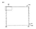
図1は、タッチスクリーンセンサ100の概略図を例示する。タッチスクリーンセンサ100は、接触感知領域105を有するタッチスクリーンパネル110を含む。接触感知領域105は、タッチセンサ駆動装置120と電気的に連結している。タッチスクリーンパネル110は、ディスプレイ装置に組み込まれる。 FIG. 1 illustrates a schematic view of the
図2は、タッチスクリーンパネルの接触感知領域、例えば、図1の接触感知領域105内に位置する導電性可視光透明区域101の斜視図を例示する。導電性可視光透明区域101は、可視光透明基材130、及び可視光透明基材130の上又は中に配置される導電性微小パターン140を含む。可視光透明基材130は、主表面132を含み、電気的に絶縁性である。可視光透明基材130は、例えば、ガラス、又はポリマーなどの任意の有用な電気的に絶縁性の材料から形成され得る。光透明基材130のための有用なポリマーの例としては、ポリエチレンテレフタレート(PET)、及びポリエチレンナフタレート(PEN)が挙げられる。導電性微小パターン140は、複数の線形金属構造から形成され得る。 FIG. 2 illustrates a perspective view of a contact sensing area of a touch screen panel, for example, a conductive visible light
図2はまた、タッチスクリーンパネルの接触感知領域内に位置する導電性可視光透明区域101の説明に使用するための軸系を例示する。一般に、ディスプレイ装置の場合、x及びy軸はディスプレイの幅及び長さに相当し、z軸は典型的にディスプレイの厚さ(即ち、高さ)方向に沿っている。この取り決めは、特に明記しない限り、全体を通して使用される。図2の軸系において、x軸及びy軸は、可視光透明基材130の主要面132と平行に定められ、正方形又は矩形表面の幅及び長さ方向に対応し得る。z軸は、この主表面と垂直であり、典型的には可視光透明基材130の厚さ方向に沿っている。導電性微小パターン140を形成する複数の線形金属構造の幅は、y軸に沿って直線的に延びる平行の線形金属構造のx方向の間隔に相当し、直交する線形金属構造のy方向の間隔は、直交する線形金属構造の幅に相当する。線形金属構造の厚さ、即ち高さは、z方向の距離に相当する。 FIG. 2 also illustrates an axial system for use in describing a conductive visible light
いくつかの実施形態では、タッチスクリーンパネルの接触感知領域内に位置する導電性可視光透明区域101は、それぞれが導電性微小パターン140を有する、可視光透明基材130の2つ以上の層を含む。 In some embodiments, the conductive visible light
導電性微小パターン140は、主表面132上に堆積される。センサは、タッチスクリーンディスプレイ、又はタッチパネルディスプレイを形成するために、ディスプレイと相互作用するため、基材130は、可視光透明であり、実質的に平面的である。基材及びセンサは、実質的に平面的、かつ可撓性であってよい。可視光透明とは、ディスプレイによってレンダリングされる情報(例えば、文字、画像、又は数字)が、タッチセンサを通して見えることを意味する。堆積された金属、更に光を遮蔽するために十分な厚さで堆積された金属の形態の導電体を含む、タッチセンサの可視性及び透明性は、金属が適切な微小パターンで堆積された場合に、達成され得る。 The
導電性微小パターン140は、情報をレンダリングするディスプレイの可視部分に重なる、少なくとも1つの可視光透明導電性区域を含む。可視光透明導電体とは、ディスプレイの一部分が、導電性微小パターンの区域を通して見ることができ、かつ微小パターンの区域が、パターンの平面において、又は換言すれば、導電性微小パターンが堆積され、これが隣接する基材の主表面に沿って導電性があることを意味する。好ましい導電性微小パターンは、二次元メッシュを有する区域、例えば、正方形グリッド、矩形(非正方形)グリッド、又は規則的な六角形ネットワークを含み、導電配線は、メッシュの配線と電気的に接触している導電体が堆積されていない、メッシュ内の囲まれた開口を画定する。開放空間、及びそれらの縁部で関連付けられる導電体配線は、本明細書においては、セルと称される。メッシュセルの他の有用な形状としては、ランダムなセル形状、及び不規則多角形が挙げられる。 The
いくつかの実施形態では、導電性微小パターンを画定する導電配線は、5つの隣接するセル、好ましくは4つの隣接するセル、より好ましくは3つの隣接するセル、更により好ましくは2つの隣接するセルの合わせた縁部の長さよりも大きな距離にわたってほぼ直線的である区分を含まないように設計される。より好ましくは、微小パターンを画定する配線は、単一のセルの縁部の長さよりも大きな距離にわたって直線的である区分を含まないように設計される。したがって、いくつかの実施形態では、微小パターンを画定する配線は、長い距離、例えば、10センチメートル、1センチメートル、又は更に1ミリメートルを超えて直線的であることはない。直前に述べた、最小の長さの直線区分を有するパターンは、ディスプレイの可視性に最小限の障害しか生じさせない利点を有するタッチスクリーンセンサにとって特に有用である。 In some embodiments, the conductive wiring defining the conductive micropattern is 5 adjacent cells, preferably 4 adjacent cells, more preferably 3 adjacent cells, even more preferably 2 adjacent cells. It is designed not to include compartments that are nearly linear over distances greater than the length of the combined edges. More preferably, the wiring defining the micropattern is designed to include no compartments that are linear over a distance greater than the length of the edge of a single cell. Thus, in some embodiments, the wiring defining the micropattern is not straight over long distances, eg, 10 centimeters, 1 centimeter, or even 1 millimeter. The pattern with the smallest length of linear section, just mentioned, is particularly useful for touch screen sensors, which have the advantage of causing minimal impairment to the visibility of the display.
導電性微小パターンの二次元形状(即ち、平面内、又は基材の主表面に沿ったパターンの形状)は、タッチスクリーンセンサにおいて有用な特別な透明導電特性を達成するために、導電体材料の光学的及び電気的特性を考慮して設計され得る。例えば、導電体材料の連続的な(パターン化されていない)堆積物又はコーティングは、そのバルク抵抗率をその厚さで除して計算されるシート抵抗を有する一方で、本発明においては、異なる水準のシート抵抗は、導電体の微小パターン化によっても設計される。 The two-dimensional shape of the conductive micropattern (ie, the shape of the pattern in a plane or along the main surface of the substrate) is of the conductive material in order to achieve special transparent conductive properties useful in touch screen sensors. It can be designed with optical and electrical properties in mind. For example, a continuous (unpatterned) deposit or coating of a conductive material has sheet resistance calculated by dividing its bulk resistivity by its thickness, whereas in the present invention it is different. Level sheet resistance is also designed by micropatterning the conductor.
いくつかの実施形態では、二次元の導電性微小パターンは、センサの導電性区域(例えば、可視光透明導電性区域)における異方性シート抵抗を達成するように設計される。異方性シート抵抗とは、直交する二方向に沿って測定された又はモデル化した際に、導電性微小パターンのシート抵抗の規模が異なることを意味する。 In some embodiments, the two-dimensional conductive micropattern is designed to achieve anisotropic sheet resistance in the conductive area of the sensor (eg, the visible light transparent conductive area). Anisotropic sheet resistance means that the sheet resistance of conductive micropatterns varies in magnitude when measured or modeled along two orthogonal directions.
対照的に、いくつかの実施形態では、センサの導電性区域(例えば、可視光透明導電性区域)における等方性シート抵抗を達成するように、二次元の導電性微小パターンが設計される。等方性シート抵抗とは、平面内で直交する任意の二方向に沿って測定又はモデル化した際に(双方向において一定の幅の配線で形成される正方形のグリッドの場合)、導電性微小パターンのシート抵抗の規模が同じであることを意味する。 In contrast, in some embodiments, a two-dimensional conductive micropattern is designed to achieve isotropic sheet resistance in the conductive area of the sensor (eg, visible light transparent conductive area). Isotropic sheet resistance is a microconductive when measured or modeled along any two directions orthogonal to each other in a plane (in the case of a square grid formed of wires of constant width in both directions). It means that the sheet resistance of the pattern is the same scale.
区域内の異方性シート抵抗は、一方向において、直交する方向のシート抵抗よりも少なくとも10パーセント高い、又は少なくとも25パーセント高い、少なくとも50パーセント高い、少なくとも100パーセント高い、少なくとも200%高い、少なくとも500%高い、又は更には少なくとも10倍高いシート抵抗を含むことができる。いくつかの実施形態では、区域内の異方性シート抵抗は、一方向において、直交する方向におけるシート抵抗よりも、少なくとも1.5倍高いシート抵抗を含む。いくつかの実施形態では、区域内の異方性シート抵抗は、一方向において、直交する方向におけるシート抵抗よりも、1.1〜10倍、他の実施形態では、1.25〜5倍、及び更に別の実施形態では、1.5〜2倍大きいシート抵抗を含む。 Anisotropic sheet resistance within an area is at least 10 percent higher, or at least 25 percent higher, at least 50 percent higher, at least 100 percent higher, at least 200 percent higher, at least 500 in one direction than orthogonal sheet resistance. It can contain sheet resistance that is% higher, or even at least 10 times higher. In some embodiments, the anisotropic sheet resistance within the area comprises at least 1.5 times higher sheet resistance in one direction than the sheet resistance in the orthogonal direction. In some embodiments, the anisotropic sheet resistance in the area is 1.1 to 10 times greater than the sheet resistance in the orthogonal direction in one direction, and 1.25 to 5 times in other embodiments. And yet another embodiment includes a sheet resistance that is 1.5 to 2 times greater.
異方性シート抵抗を生じ得る導電性微小パターン形状の例は、導電配線の幅が一定である、ほぼ矩形(非正方形)の微小グリッドである。このような矩形微小グリッド(非正方形)に関し、異方性シート抵抗は、他方よりも10パーセント長い、他方よりも25パーセント長い、他方よりも少なくとも50パーセント長い、他方よりも100パーセント長い、又は更には他方よりも10倍長い一縁部を含む、グリッドのセルの反復形状から生じ得る。異方性シート抵抗は、異なる方向で配線の幅を変えることによって(例えば、別の、非常に対称的なメッシュのセルのパターンで)、生成することができる。異方性シート抵抗を生成するための後者の手法の例は、例えば、200マイクロメートルのピッチを有する導電配線の正方形グリッドであり、第1の方向における配線は10マイクロメートルの幅であり、直交する方向の配線は、9マイクロメートル幅、7.5マイクロメートル幅、5マイクロメートル幅、又は更に1マイクロメートル幅である。区域内の異方性シート抵抗は、平行な導電線のパターンによって生じるように、一方向において有限の測定可能なシート抵抗を、及び他方向において本質的に無限のシート抵抗を含み得る。上記のように、いくつかの実施形態では、区域内の異方性シート抵抗は、一方向において有限の測定可能なシート抵抗を、及び第1の方向と直交する方向において有限の測定可能なシート抵抗を含む。 An example of a conductive micropattern shape that can generate anisotropic sheet resistance is a nearly rectangular (non-square) microgrid with a constant width of the conductive wiring. For such rectangular microgrids (non-square), the anisotropic sheet resistance is 10 percent longer than the other, 25 percent longer than the other, at least 50 percent longer than the other, 100 percent longer than the other, or even more. Can result from the repeating shape of cells in the grid, including one edge that is ten times longer than the other. Anisotropic sheet resistance can be generated by varying the width of the wiring in different directions (eg, with a different, highly symmetrical mesh cell pattern). An example of the latter method for generating anisotropic sheet resistance is, for example, a square grid of conductive wiring with a pitch of 200 micrometers, the wiring in the first direction being 10 micrometers wide and orthogonal. The wiring in the direction is 9 micrometers wide, 7.5 micrometers wide, 5 micrometers wide, or even 1 micrometer wide. Anisotropic sheet resistance within an area can include finite measurable sheet resistance in one direction and essentially infinite sheet resistance in the other direction, as caused by a pattern of parallel conductive wires. As mentioned above, in some embodiments, the anisotropic sheet resistance within the area is a finite measurable sheet resistance in one direction and a finite measurable sheet resistance in the direction orthogonal to the first direction. Including resistance.
導電性微小パターンの区域が等方性であるか又は異方性であるかを決定する目的で、関連する特性の測定又は計算を行うために、微小パターンの規模に対する関心の区域の規模が、合理的に選択されなくてはならないことが、当業者によって理解されるであろう。例えば、仮にも一度導電体がパターン化されると、異なる方向における測定においてシート抵抗における違いを生じる測定を行うための位置及び規模を選択することは、容易である。以下の詳細な実施例により、この点がより明確になり得る。100マイクロメートル幅の導電体配線、及び1ミリメートルのピッチ(グリッド内で900マイクロメートル×900マイクロメートルの正方形開口部となる)を有する正方形グリッドの形態の等方性形状の導電体パターンを想定し、正方形開口部の縁部に沿った配線のうちの1つの中のシート抵抗の4点プローブ測定を行い、プローブは、4つの直線状に配置されたプローブに沿って25マイクロメートルの一定間隔を有する(2つの電流プローブ間、外側のプローブの間の分離が75マイクロメートルとなる)ものと想定すると、プローブが配線と平行に整列されたか又は配線と直交するように整列されたかに応じて、異なる水準のシート抵抗が、測定された電流及び電圧の値によって算出される。したがって、正方形グリッド形状が、正方形グリッドセル寸法よりも大きな規模の等方性シート抵抗を生じるにも拘わらず、異方性を提示するシート抵抗の測定を実行することが可能である。したがって、本開示における、導電性微小パターン(例えば、メッシュを含む微小パターンの可視光透明導電性区域)のシート抵抗の異方性を定義する目的で、シート抵抗が測定又はモデル化されるべき、関連する規模は、メッシュのセルの長さ規模よりも大きく、好ましくは2つのセルの長さ規模よりも大きい。いくつかの場合においては、シート抵抗は、メッシュがそのシート抵抗において異方性であることを示すために、メッシュの中の5つ以上のセルの長さ規模にわたって測定又はモデル化される。 The size of the area of interest with respect to the size of the micropattern is to measure or calculate the relevant properties for the purpose of determining whether the area of the conductive micropattern is isotropic or anisotropic. It will be understood by those skilled in the art that it must be reasonably selected. For example, once the conductor is patterned, it is easy to select the position and scale for making measurements that make a difference in sheet resistance in measurements in different directions. This point can be made clearer by the following detailed examples. Assume an isotropic conductor pattern in the form of a square grid with 100 micrometer wide conductor wiring and a 1 mm pitch (which results in a 900 micrometer x 900 micrometer square opening in the grid). A four-point probe measurement of the sheet resistance in one of the wires along the edge of the square opening was made and the probes were spaced 25 micrometers along the four linearly arranged probes. Assuming that it has (the separation between the two current probes and the outer probe is 75 micrometers), depending on whether the probes are aligned parallel to the wire or perpendicular to the wire. Different levels of sheet resistance are calculated from the measured current and voltage values. Therefore, it is possible to perform sheet resistance measurements that present anisotropy, even though the square grid shape produces isotropic sheet resistance on a scale larger than the square grid cell dimensions. Therefore, sheet resistance should be measured or modeled for the purpose of defining the anisotropy of sheet resistance in the present disclosure of conductive micropatterns (eg, visible light transparent conductive areas of micropatterns including meshes). The relevant scale is greater than the cell length scale of the mesh, preferably greater than the length scale of the two cells. In some cases, sheet resistance is measured or modeled over the length scale of five or more cells in the mesh to show that the mesh is anisotropic in its sheet resistance.
導電性微小パターンが、区域内でシート抵抗の異方性を呈する実施形態とは対照的に、透明導電性酸化物薄膜(例えば、酸化インジウムスズ、即ち、ITO)を含むセンサは、導電体の隣接する区域において等方性シート抵抗を呈する。後者の場合、隣接する区域のシート抵抗の4点プローブ測定が、異なる方向で、より小さいプローブの間隔で行われて、これを測定、又はモデル化することができ、異なる方向における電流及び電圧の同じ読取り値が、明確に等方性を示す。 In contrast to embodiments where the conductive micropattern exhibits anisotropy of sheet resistance within the region, sensors containing transparent conductive oxide thin films (eg, indium tin oxide, ie ITO) are of conductive material. Exhibits isotropic sheet resistance in adjacent areas. In the latter case, four-point probe measurements of sheet resistance in adjacent areas can be made in different directions, with smaller probe spacing, which can be measured or modeled for current and voltage in different directions. The same readings clearly indicate isotropic.
いくつかの実施形態では、二次元導電性微小パターンは、所定の方向で測定された際に、センサの2つの異なるパターン化された導電体区域において、異なる水準又は規模のシート抵抗を達成するように設計される。例えば、異なる水準のシート抵抗に関し、2つのうちより高い方が、より低い方よりも1.25倍超、1.5倍超、2倍超、5倍超、10倍超、又は更に100倍超大きいことがある。いくつかの実施形態では、2つの面抵抗値のうちのより高い方が、より低い方よりも1.25〜1000倍、他の実施形態では、1.25〜100倍、他の実施形態では、1.25〜10倍、他の実施形態では、2〜5倍大きい。ある区域が、別の区域のものと異なるシート抵抗を有するものとみなされるためには、これは、他の区域のシート抵抗より、少なくとも1.1倍大きいか又は小さいシート抵抗を有する。 In some embodiments, the two-dimensional conductive micropatterns achieve different levels or scales of sheet resistance in two different patterned conductor areas of the sensor when measured in a given direction. Designed to. For example, for different levels of sheet resistance, the higher of the two is more than 1.25 times, more than 1.5 times, more than 2 times, more than 5 times, more than 10 times, or even 100 times higher than the lower one. It can be super large. In some embodiments, the higher of the two surface resistance values is 1.25 to 1000 times higher than the lower, in other embodiments 1.25 to 100 times, in other embodiments. , 1.25 to 10 times, and in other embodiments, 2 to 5 times larger. In order for one area to be considered to have different sheet resistance than that of another area, it has at least 1.1 times greater or less sheet resistance than the sheet resistance of another area.
いくつかの実施形態では、微小パターンは、電気的に隣接する、パターン化された2つの導電体区域の、前述の異なる水準のシート抵抗を達成するように設計されており、つまり、これらは、これらの境界に沿って互いに電気的に接触しているパターン化された導電体区域である。導電境界を共有する、パターン化された2つの導電体区域はそれぞれ、一様な、それぞれのパターン形状を有し得るが、やはり異なり得る。いくつかの実施形態では、微小パターンは、電気的に接触していない2つの異なるパターン化された導電体区域の、異なる水準のシート抵抗を達成するように設計されており、即ち、これらは、パターン化された区域が境界に沿って電気的に接触しているこれらの間に境界を共有しない、パターン化された導電体区域である。それらの間に導電境界を共有しない、パターン化された2つの導電体はそれぞれ、一様な、それぞれのパターン形状を有し得るが、やはり異なってもよい。電気的に接触していない区域について、これら双方が、同じ固体導電体素子、例えば、バスバー又はパッドに、このパターンで電気的に接触することは、本開示の範囲内である。いくつかの実施形態では、微小パターンは、互いに電気的に絶縁された2つの区域において、異なる水準の面抵抗を達成するように設計され、したがって、電気信号によって独立して対処することができる。電気的に絶縁された2つのメッシュ区域はそれぞれ、一様なパターン形状を有し得るが、やはり異なってもよい。最後に、いくつかの実施形態では、微小パターンは、例えば、電気的に隣接する2つの区域の第1区域から第2区域へと連続的に変化するシート抵抗を生成することにより、2つの異なる区域において、異なる水準のシート抵抗を達成するように設計される。 In some embodiments, the micropatterns are designed to achieve the different levels of sheet resistance described above for two electrically adjacent, patterned conductor areas, i.e., they are: Patterned conductor areas that are in electrical contact with each other along these boundaries. The two patterned conductor areas that share a conductive boundary can each have a uniform, pattern shape, but can also be different. In some embodiments, the micropatterns are designed to achieve different levels of sheet resistance in two different patterned conductor areas that are not in electrical contact, ie, they are. Patterned conductor areas that do not share a boundary between them where the patterned areas are in electrical contact along the boundaries. The two patterned conductors, which do not share a conductive boundary between them, may each have a uniform, respective pattern shape, but may also be different. It is within the scope of the present disclosure that, for areas that are not in electrical contact, both of them are in electrical contact with the same solid conductor element, such as a busbar or pad, in this pattern. In some embodiments, the micropatterns are designed to achieve different levels of surface resistance in two areas that are electrically isolated from each other and can therefore be addressed independently by electrical signals. The two electrically isolated mesh areas may each have a uniform pattern shape, but may also be different. Finally, in some embodiments, the micropattern is two different, for example by producing sheet resistance that continuously changes from the first zone to the second zone of two electrically adjacent zones. Designed to achieve different levels of sheet resistance in the area.
測定方向において異なるシート抵抗を有する2つの区域を含む二次元導電性微小パターンは、この区域に関して好ましい水準の面抵抗(例えば、5〜100Ω/スクエアの低い面抵抗)を有する、感知領域内の可視光透明導電性区域(変化する、又は異方性の面抵抗を任意に含む)の設計、及び感知領域内に位置してもしなくてもよいタッチスクリーンセンサの部分としての、電気素子、例えば抵抗素子の設計にとって有用であり、抵抗素子は、抵抗作用のために最適に選択されるシート抵抗(例えば、150〜1000Ω/スクエアのより高いシート抵抗)を有するシート導電体を含み、場合により他の設計制約、例えば抵抗の占有面積の最小化による制約を考慮する。 Two-dimensional conductive micropatterns containing two areas with different sheet resistances in the measurement direction are visible within the sensing area with a favorable level of surface resistance for this area (eg, low surface resistance of 5-100 Ω / square). Design of lightly transparent conductive areas (including optionally varying or anisotropic surface resistance), and electrical elements such as resistors as part of the touch screen sensor that may or may not be located within the sensing area. Useful for element design, resistant elements include sheet conductors with sheet resistance optimally selected for resistance action (eg, higher sheet resistance of 150-1000 Ω / square), and optionally others. Consider design constraints, such as constraints by minimizing the occupied area of the resistor.
上記のように、測定又はモデル化し得る有限なシート抵抗を有する区域及び方向における導電性微小パターンのシート抵抗は、0.01Ω/スクエア〜1メガΩ/スクエアの範囲、又は0.1〜1000Ω/スクエアの範囲、又は1〜500Ω/スクエアの範囲にあり得る。いくつかの実施形態では、導電性微小パターンのシート抵抗は、1〜50Ω/スクエアの範囲にある。他の実施形態では、導電性微小パターンのシート抵抗は、5〜500Ω/スクエアの範囲にある。他の実施形態では、導電性微小パターンのシート抵抗は、5〜100Ω/スクエアの範囲にある。他の実施形態では、導電性微小パターンのシート抵抗は、5〜40Ω/スクエアの範囲にある。他の実施形態では、導電性微小パターンのシート抵抗は、10〜30Ω/スクエアの範囲にある。導電性微小パターン又は導電性微小パターンの区域を特徴付け得るシート抵抗の指示において、微小パターン又は微小パターンの区域は、それが、シート抵抗値を、任意の方向における電気伝導において有する場合、所定の値のシート抵抗を有するものとされる。 As mentioned above, the sheet resistance of conductive micropatterns in areas and directions with finite sheet resistance that can be measured or modeled ranges from 0.01Ω / square to 1 megaΩ / square, or 0.1 to 1000Ω /. It can be in the square range, or 1-500Ω / square range. In some embodiments, the sheet resistance of the conductive micropattern is in the range of 1-50Ω / square. In other embodiments, the sheet resistance of the conductive micropattern is in the range of 5 to 500 Ω / square. In other embodiments, the sheet resistance of the conductive micropattern is in the range of 5-100Ω / square. In other embodiments, the sheet resistance of the conductive micropattern is in the range of 5-40Ω / square. In other embodiments, the sheet resistance of the conductive micropattern is in the range of 10-30Ω / square. In the indication of sheet resistance which can characterize a conductive micropattern or an area of a conductive micropattern, the micropattern or the area of the micropattern is predetermined if it has a sheet resistance value in electrical conduction in any direction. It is assumed to have a value sheet resistance.
センサの透明性、及びセンサを通じたディスプレイの可視性を達成するための導電体の適切な微小パターンは、一定の特質を有する。まず、これを通じてディスプレイが見られる導電性微小パターンの区域は、導電体によって遮蔽される、50%未満、又は25%未満、又は20%未満、又は10%未満、又は5%未満、又は4%未満、又は3%未満、又は2%未満、又は1%未満、又は0.25%〜0.75%の範囲、又は0.5%未満のセンサの面積率を有するべきである。 Appropriate micropatterns of conductors for achieving sensor transparency and display visibility through the sensor have certain properties. First, the area of the conductive micropattern through which the display is seen is shielded by the conductor, less than 50%, or less than 25%, or less than 20%, or less than 10%, or less than 5%, or 4%. Should have a sensor area ratio of less than, or less than 3%, or less than 2%, or less than 1%, or in the range of 0.25% to 0.75%, or less than 0.5%.
導電体微小パターン、又は導電性微小パターンの区域の開口率(又は開口若しくは開口の割合)は、導電体によって遮蔽されない微小パターン面積、又は区域面積の割合である。開口は、1から、導電体によって遮蔽される面積率を引いたものに相当し、少数又は百分率として、適宜互換的に表現することができる。導電体によって遮蔽される面積率は、微小パターン化された導電体の線の密度と互換的に使用される。微小パターン化された導電体は、電気的に導電性の微小パターン及び導電性微小パターンと互換的に使用される。したがって、導電体によって遮蔽される割合に関して上の文章で示された値に関し、開口値は、50%超、75%超、80%超、90%超、95%超、96%超、97%超、98%超、99%超、99.25〜99.75%、99.8%、99.85%、99.9%、及び更に99.95%である。いくつかの実施形態では、導電体微小パターンの区域の開口(例えば、可視光透明導電性区域)は、80%〜99.5%であり、他の実施形態では90%〜99.5%であり、他の実施形態では、95%〜99%であり、他の実施形態では、96%〜99.5%であり、他の実施形態では、97%〜98%であり、他の実施形態では、最大99.95%である。実際的な製造方法を使用した、有用な光学的特性(例えば、高い透過率及び導電パターン要素の不可視性)、及び電気的特性の再現可能な達成に関し、開口の好ましい値は、90〜99.5%、より好ましくは95〜99.5%、最も好ましくは95〜99.95%である。 The aperture ratio (or the ratio of openings or openings) of the conductor micro pattern or the area of the conductive micro pattern is the ratio of the micro pattern area or the area that is not shielded by the conductor. The opening corresponds to 1 minus the area ratio shielded by the conductor, and can be appropriately and interchangeably expressed as a minority or a percentage. The area ratio shielded by the conductor is used interchangeably with the line density of the micropatterned conductor. The micropatterned conductor is used interchangeably with electrically conductive micropatterns and conductive micropatterns. Therefore, with respect to the values indicated in the above text regarding the percentage of shielding by the conductor, the opening values are greater than 50%, greater than 75%, greater than 80%, greater than 90%, greater than 95%, greater than 96%, 97%. Super, over 98%, over 99%, 99.25-99.75%, 99.8%, 99.85%, 99.9%, and even 99.95%. In some embodiments, the opening of the conductor micropattern area (eg, visible light transparent conductive area) is 80% to 99.5%, and in
ディスプレイのピクセルパターンとの干渉を極小化し、ユーザー又は見る人の裸眼によるパターン要素(例えば、導電体の線)の可視性を回避するために、導電パターン要素の最小寸法(例えば、線又は導電配線の幅)は、およそ50マイクロメートル以下、又はおよそ25マイクロメートル以下、又はおよそ10マイクロメートル以下、又はおよそ5マイクロメートル以下、又はおよそ4マイクロメートル以下、又はおよそ3マイクロメートル以下、又はおよそ2マイクロメートル以下、又はおよそ1マイクロメートル以下、又はおよそ0.5マイクメートル以下であるべきである。 The minimum dimensions of a conductive pattern element (eg, wire or conductive wiring) to minimize interference with the pixel pattern of the display and avoid visibility of the pattern element (eg, wire of the conductor) by the naked eye of the user or viewer. Width) is about 50 micrometers or less, or about 25 micrometers or less, or about 10 micrometers or less, or about 5 micrometers or less, or about 4 micrometers or less, or about 3 micrometers or less, or about 2 micrometers. It should be less than a meter, or less than about 1 micrometer, or less than about 0.5 mic meters.
いくつかの実施形態では、導電パターン素子の最小寸法は、0.5〜50マイクロメートル、他の実施形態では、0.5〜25マイクロメートル、他の実施形態では、1〜10マイクロメートル、他の実施形態では、1〜5マイクロメートル、他の実施形態では、1〜4マイクロメートル、他の実施形態では、1〜3マイクロメートル、他の実施形態では、0.5〜3マイクロメートル、及び他の実施形態では、0.5〜2マイクロメートルである。有用な光学的特性(例えば、裸眼による導電パターン要素の高い透過率及び不可視性)、及び電気的特性の再現可能な達成に関し、実際的な製造方法の使用による制約を考慮し、導電パターン素子の最小寸法の好ましい値は、0.5〜5マイクロメートル、より好ましくは1〜4マイクロメートルであり、最も好ましくは1〜3マイクロメートルである。 In some embodiments, the minimum dimensions of the conductive pattern element are 0.5 to 50 micrometers, in other embodiments 0.5 to 25 micrometers, in
一般的に、堆積された導電性材料は、望ましくないことに、タッチセンサの光透過率を低減させる。基本的に、堆積された導電性材料が存在するいずれの場所でも、そのユーザーによる可視性に関して、ディスプレイは遮蔽される。導電体材料によって生じる減衰の程度は、導電体微小パターン内の導電体によって被覆されるセンサ又はセンサ区域の面積率に比例する。 In general, the deposited conductive material undesirably reduces the light transmission of the touch sensor. Essentially, wherever the deposited conductive material is present, the display is shielded for its user visibility. The degree of attenuation caused by the conductor material is proportional to the area ratio of the sensor or sensor area covered by the conductor within the conductor micropattern.
一般的に、透明タッチスクリーンセンサは、低いヘイズ値を呈することが望ましい。ヘイズとは、例えば、Haze−Gard機器(Haze−Gard plus、メリーランド州コロンビアのBYK Gardner)により測定される、光が媒体を通過する際のその分散に関する特性を指す。いくつかの実施形態では、タッチスクリーンセンサは、10%未満、いくつかの実施形態では5%未満、いくつかの実施形態では4%未満、いくつかの実施形態では3%未満、いくつかの実施形態では2%未満のヘイズを呈する。導電体微小パターンを含む区域の、高い透過率(可視光透過性とも称される)、低いヘイズ、低い導電体配線可視性の望ましい組み合わせを達成する実施形態が開示される。したがって、導電体微小パターンは、感知領域又はタッチスクリーンセンサディスプレイの区域の一部として使用された場合(例えば、微小パターンをディスプレイの可視区域に重ねた場合)に特に有用である。 In general, it is desirable for the transparent touch screen sensor to exhibit a low haze value. Haze refers to, for example, a property relating to the dispersion of light as it passes through a medium, as measured by a Haze-Gard device (Haze-Gard plus, BYK Gardener, Columbia, Maryland). In some embodiments, the touch screen sensor is less than 10%, in some embodiments less than 5%, in some embodiments less than 4%, in some embodiments less than 3%, in some embodiments. In morphology, it exhibits less than 2% haze. Embodiments are disclosed that achieve the desired combination of high transmittance (also referred to as visible light transmission), low haze, and low conductor wiring visibility in areas containing conductor micropatterns. Therefore, conductor micropatterns are particularly useful when used as part of a sensing area or area of a touch screen sensor display (eg, when the micropattern is superimposed on the visible area of the display).
いくつかの実施形態では、例えば、導電性材料の一様ではないメッシュから生じる、シート抵抗の不均一な分布が存在したとしても、可視ディスプレイ領域にわたって均一な光透過性を有する可視光透明ディスプレイセンサを作るために、センサは、パターン全体の光透過性の均一性を維持するように機能する、導電性微小パターンに付加された絶縁された導電体堆積物を含む。このような絶縁された導電体堆積物は、センサの駆動装置(例えば、電気回路又はコンピューター)に接続されず、したがって電気的機能を提供しない。例えば、3マイクロメートルの線幅及び200マイクロメートルのピッチの正方形グリッド形状のメッシュを有する第1区域(金属により面積の3%が遮蔽されている、即ち、97%の開口)、並びに3マイクロメートルの線幅及び300マイクロメートルのピッチの正方形グリッド形状のメッシュを有する第2区域(金属により面積の2%が遮蔽されている、即ち、98%の開口)を含む金属導電体微小パターンは、300マイクロメートルピッチのグリッド区域の開放セルそれぞれの内部に、パターン内で等間隔で配置された100個の3マイクロメートル×3マイクロメートルの正方形の金属導電体を含めることにより、2つの区域にわたるその平均光透過率を光学的に均一にすることができる。100個の3マイクロメートル×3マイクロメートルの正方形(900平方マイクロメートル)は、各300マイクロメートル×300マイクロメートルのセル(90000平方マイクロメートル)において、面積を更に1パーセント遮蔽し、したがって、第2区域の平均光透過率を、第1区域のものと等しくする。透明導電性区域及びそれらの間の空間の区域を含む、センサにわたる光透過性の均一性を維持するために、隣接する透明導電性区域(例えば、二次元のメッシュ又はネットワークの形態の微小パターン化された導電体を含む隣接する透明導電性区域)の間の空間の区域に、同様の絶縁金属構造を加えることができる。絶縁された正方形の導電体に加えて、光学的均一性を調整するための、他の有用な絶縁された導電体堆積物としては、円及び線が挙げられる。電気的に絶縁された堆積物の最小寸法(例えば、正方形構造の縁部長さ、円形構造の直径、又は線状構造の幅)は、10マイクロメートル未満、5マイクロメートル未満、2マイクロメートル未満、又は更には1マイクロメートル未満である。 In some embodiments, a visible light transparent display sensor that has uniform light transmission over the visible display area, even if there is a non-uniform distribution of sheet resistance, for example resulting from a non-uniform mesh of conductive material. To make the sensor, the sensor contains an insulated conductor deposit added to the conductive micropattern, which functions to maintain the uniformity of light transmission throughout the pattern. Such insulated conductor deposits are not connected to the sensor drive (eg, electrical circuit or computer) and therefore do not provide electrical functionality. For example, a first area with a square grid-shaped mesh with a line width of 3 micrometers and a pitch of 200 micrometers (3% of the area is shielded by metal, ie 97% openings), and 3 micrometers. A metal conductor micropattern containing a second area (2% of the area is shielded by metal, i.e. 98% opening) with a square grid-shaped mesh with a line width of 300 micrometers and a pitch of 300 micrometers. By including 100 3 micrometer x 3 micrometer square metal conductors evenly spaced within the pattern within each open cell of the micrometer pitch grid area, its average over the two areas. The light transmission rate can be made optically uniform. 100 3 micrometer x 3 micrometer squares (900 micrometers) each shield an additional 1% of area in 300 micrometer x 300 micrometer cells (90000 square micrometers), thus a second Make the average light transmission of the area equal to that of the first area. Micropatterning of adjacent transparent conductive areas (eg, two-dimensional mesh or network morphology) to maintain uniformity of light transmission across the sensor, including transparent conductive areas and areas of space between them. A similar insulating metal structure can be added to the area of space between the adjacent transparent conductive areas containing the conductors. In addition to the insulated square conductors, other useful insulated conductor deposits for adjusting optical uniformity include circles and lines. The minimum dimensions of electrically isolated deposits (eg, edge length of square structures, diameter of circular structures, or width of linear structures) are less than 10 micrometers, less than 5 micrometers, less than 2 micrometers, Or even less than 1 micrometer.
実際的な製造方法を使用する、有用な光学的特性(例えば、導電パターン素子の高い透過率、及び不可視性)の再現可能な達成に関し、電気的に絶縁された堆積物の最小寸法は、好ましくは0.5〜10マイクロメートル、より好ましくは0.5〜5マイクロメートル、更により好ましくは0.5〜4マイクロメートル、更により好ましくは1〜4マイクロメートル、最も好ましくは1〜3マイクロメートルである。いくつかの実施形態では、電気的に絶縁された導電体堆積物の配置は、周期性を有さないように設計される。周期性の不在は、下部のディスプレイの周期的ピクセルパターンとの、好ましくない可視的な相互作用を制限するために、好ましい。電気的に絶縁された導電体堆積物の集合が周期性を欠くためには、堆積物を有し、デコード、又は信号生成及び/若しくは処理電子機器に接続する微小パターン要素を欠く区域にわたり、堆積物の少なくとも一部の本来ならば周期性を有する配置に対して単一の障害が存在するだけでよい。このような電気的に絶縁された導電体堆積物は、非周期的な配置を有するとされるか、又は電気的に絶縁された導電体堆積物の非周期的な配置であるとされる。いくつかの実施形態では、電気的に絶縁された導電体堆積物は、例えば、5マイクロメートルの縁部長さを有する正方形堆積物の対向する面において存在するような、10マイクロメートル未満の間隔で離れた直線的で平行な縁部を欠くように設計される。より好ましくは、絶縁された導電体堆積物は、5マイクロメートル、より好ましくは4マイクロメートル、更により好ましくは3マイクロメートル、更により好ましくは2マイクロメートル未満の間隔で離れた直線的で平行な縁部を欠くように設計される。直線的で平行な縁部を欠く電気的に絶縁された導電体堆積物の例は、楕円形、円形、五角形、七角形、及び三角形である。電気的に絶縁された導電体堆積物の構造における、直線的で平行な縁部の不在は、センサと一体化するディスプレイの可視性を阻害し得る光回折アーチファクトを最小化するように機能する。 For reproducible achievement of useful optical properties (eg, high permeability and invisibility of conductive patterned elements) using practical manufacturing methods, the minimum dimensions of electrically isolated deposits are preferred. Is 0.5 to 10 micrometers, more preferably 0.5 to 5 micrometers, even more preferably 0.5 to 4 micrometers, even more preferably 1 to 4 micrometers, most preferably 1-3 micrometers. Is. In some embodiments, the arrangement of electrically isolated conductor deposits is designed to have no periodicity. The absence of periodicity is preferred because it limits the unwanted visible interaction with the periodic pixel pattern of the lower display. In order for an assembly of electrically isolated conductor deposits to lack periodicity, they deposit over areas that have deposits and lack micropattern elements that connect to decoding or signal generation and / or processing electronics. There only needs to be a single obstacle to the otherwise periodic arrangement of at least some of the objects. Such electrically insulated conductor deposits are said to have an aperiodic arrangement or an aperiodic arrangement of electrically insulated conductor deposits. In some embodiments, the electrically isolated conductor deposits are spaced less than 10 micrometers, for example, present on opposite surfaces of a square deposit with an edge length of 5 micrometers. Designed to lack separate straight, parallel edges. More preferably, the insulated conductor deposits are linear and parallel at intervals of 5 micrometers, more preferably 4 micrometers, even more preferably 3 micrometers, even more preferably less than 2 micrometers. Designed to lack edges. Examples of electrically isolated conductor deposits lacking straight, parallel edges are ellipses, circles, pentagons, heptagons, and triangles. The absence of straight, parallel edges in the structure of electrically isolated conductor deposits serves to minimize photodiffraction artifacts that can impair the visibility of the display integrated with the sensor.
導電体微小パターンの、光学的均一性に対する影響は、数量化することができる。ディスプレイの可視区域に重なるセンサ、したがって導電体微小パターンの合計面積が、1ミリメートル×1ミリメートル区域の配列へと区分化される場合、好ましいセンサは、いずれの区域も全区域の平均から75%超異なる遮蔽面積率を有さないような導電体微小パターンを含む。より好ましくは、いずれも50パーセント超異なる遮蔽面積率を有さない。より好ましくは、いずれも25パーセント超異なる遮蔽面積率を有さない。更により好ましくは、いずれも10パーセント超異なる遮蔽面積率を有さない。ディスプレイの可視区域に重なるセンサ、したがって導電体微小パターンの合計面積が、5ミリメートル×5ミリメートル区域の配列へと区分化される場合、好ましいセンサは、いずれの区域も全区域の平均から50%超異なる遮蔽面積率を有さないような導電体微小パターンを含む。好ましくは、いずれも50パーセント超異なる遮蔽面積率を有さない。より好ましくは、いずれも25パーセント超異なる遮蔽面積率を有さない。更により好ましくは、いずれも10パーセント超異なる遮蔽面積率を有さない。 The effect of the conductor micropattern on the optical uniformity can be quantified. If the sensors that overlap the visible area of the display, and thus the total area of the conductor micropatterns, are segmented into an array of 1 mm x 1 mm areas, the preferred sensor is more than 75% of the average for all areas in each area. Includes conductor micropatterns that do not have different shielding area ratios. More preferably, none of them have a shielding area ratio that differs by more than 50 percent. More preferably, none of them have a shielding area ratio that differs by more than 25 percent. Even more preferably, none of them have a shielding area ratio that differs by more than 10 percent. If the sensors that overlap the visible area of the display, and thus the total area of the conductor micropatterns, are segmented into an array of 5 mm x 5 mm areas, the preferred sensor is more than 50% of the average for all areas in each area. Includes conductor micropatterns that do not have different shielding area ratios. Preferably, none have a shielding area ratio that differs by more than 50 percent. More preferably, none of them have a shielding area ratio that differs by more than 25 percent. Even more preferably, none of them have a shielding area ratio that differs by more than 10 percent.
本開示は、有利なことに、透明導電性酸化物(TCO)、例えば、ITOとは対照的に、透明導電センサにおける導電性材料としての金属の使用を可能にする。ITOは、例えば、ある構成体における腐食に関係する分解、撓んだときに割れる傾向、100未満〜1000Ω/スクエアのシート抵抗を有するコーティングとして堆積された際の透過光の大幅な減衰(反射及び吸収による)、及びインジウムの希少性による費用の増加などの、いくつかの欠点を有する。ITOはまた、均一かつ再現可能な電気的特性を有するように堆積することが困難であり、タッチスクリーンセンサを構成する導電パターンに連結する、より複雑かつ高価な電子機器の必要性へと繋がる。 The disclosure advantageously allows the use of transparent conductive oxides (TCOs), eg, metals as conductive materials in transparent conductive sensors, as opposed to ITO. ITO has, for example, corrosion-related decomposition in certain constructs, a tendency to crack when flexed, and significant attenuation (reflection and reflection) of transmitted light when deposited as a coating with a sheet resistance of less than 100 to 1000 Ω / square. It has several drawbacks, such as (due to absorption) and increased costs due to the rarity of indium. ITO is also difficult to deposit to have uniform and reproducible electrical properties, leading to the need for more complex and expensive electronics to be coupled to the conductive patterns that make up the touch screen sensor.
導電性微小パターンを形成するために有用な金属の例としては、金、銀、パラジウム、プラチナ、アルミニウム、銅、ニッケル、すず、合金、及びこれらの組み合わせが挙げられる。いくつかの実施形態では、導電体は、透明導電性酸化物である。いくつかの実施形態では、導電体はITOである。導電体は、5ナノメートル〜5マイクロメートル、又は10ナノメートル〜500ナノメートル、又は15ナノメートル〜250ナノメートルの厚さを有し得る。いくつかの実施形態では、導電体の厚さは1マイクメートル未満である。当該技術分野において既知であるように、導電体の望ましい厚さは、望ましい面抵抗から始まり、微小パターン形状(及び、ひいては平面の通電断面への影響)、及び導電体のバルク抵抗率を考慮することによって算出され得る。微小パターンの複雑な形状に関し、当該技術分野では計算法、例えば、シート抵抗を算出するのに使用することができる有限差分法又は有限要素法が存在し、本明細書においては、微小パターンの特性のモデル化と称される。当該技術分野において既知であるように、シート抵抗は、4点プローブ技術及び非接触渦電流法などの多数の技術を使用して測定することができる。 Examples of metals useful for forming conductive micropatterns include gold, silver, palladium, platinum, aluminum, copper, nickel, tin, alloys, and combinations thereof. In some embodiments, the conductor is a transparent conductive oxide. In some embodiments, the conductor is ITO. The conductor can have a thickness of 5 nanometers to 5 micrometers, or 10 nanometers to 500 nanometers, or 15 nanometers to 250 nanometers. In some embodiments, the thickness of the conductor is less than 1 micrometer. As is known in the art, the desired thickness of a conductor begins with the desired surface resistance, taking into account the micropattern shape (and thus the effect on the electrical cross section of the plane) and the bulk resistivity of the conductor. Can be calculated by With respect to the complex shape of a micropattern, there are computational methods in the art, such as the finite difference method or the finite element method that can be used to calculate sheet resistance, and in the present specification, the characteristics of the micropattern. Is called modeling of. As is known in the art, sheet resistance can be measured using a number of techniques such as the four-point probe technique and the non-contact eddy current method.
本発明のセンサと一体化することができる有用なディスプレイの例としては、液晶ディスプレイ、ブラウン管ディスプレイ、プラズマディスプレイパネル、及び有機発光ダイオードディスプレイが挙げられる。 Examples of useful displays that can be integrated with the sensor of the present invention include liquid crystal displays, cathode ray tube displays, plasma display panels, and organic light emitting diode displays.
本発明による導電パターンは、任意の適切なパターン化方法、例えば、エッチングを伴うフォトリソグラフィー、又はめっきを伴うフォトリソグラフィー(例えば、米国特許第5,126,007号、同第5,492,611号、同第6,775,907号を参照)を含む方法によって生成することができる。加えて、導電パターンは、他のいくつかの代表的な方法(それぞれ、以下でより詳細に説明される)の1つを利用して作製することができる。 The conductive pattern according to the invention can be any suitable patterning method, such as photolithography with etching, or photolithography with plating (eg, US Pat. Nos. 5,126,007, 5,492,611). , No. 6,775,907). In addition, the conductive pattern can be made utilizing one of several other typical methods (each described in more detail below).
1.レーザー硬化マスキング(金属フィルム上のマスク層の硬化、及び次にエッチング)
2.(マスキング材料又は続く金属めっきのための種材料の)インクジェット印刷
3.(続く金属めっきのための種材料の)グラビア印刷
4.微小複製(基材中に微小溝を形成し、次に導電性材料又は続く金属めっきのための種材料を充填する)、又は
5.マイクロコンタクト印刷(基材表面上の自己組織化単分子膜(SAM)パターンのスタンピング又は輪転印刷)。1. 1. Laser curing masking (curing of mask layer on metal film, and then etching)
2. Inkjet printing (of masking material or seed material for subsequent metal plating) 3. Gravure printing (of seed material for subsequent metal plating) 4. Microreplication (forming microgrooves in the substrate and then filling with a conductive material or seed material for subsequent metal plating), or 5. Microcontact printing (self-assembled monolayer (SAM) pattern stamping or rotary printing on the surface of the substrate).
高容量、高解像度印刷方法の利用は、一般的に、導電性素子の正確な配置を可能にし、また、市販のディスプレイピクセルと適合する規模の微小導電体のバリエーションの微小半導体の(擬似ランダム)変動を可能にし、本来ならば生じ得る光学的異常(例えば、モアレパターン)を制限する。 The use of high-capacity, high-resolution printing methods generally allows for accurate placement of conductive elements and (pseudo-random) microsemiconductor variations of microconductors on a scale compatible with commercially available display pixels. Allows variation and limits possible optical anomalies (eg, moiré patterns).
本明細書で説明されるいくつかの実施形態は、平坦な面の「ワイヤー様」導電体を利用してもよく、これは、透明導電体を利用する既存のセンサよりも高い光透過率を可能にする。これらの平坦な面の「ワイヤー様」導電体は、いくつかの実施形態では、既存の円形ワイヤー手段で可能であるよりも優れた導電体配置の拡張性及び制御を提供する。本明細書で記載される微小導電体は、10マイクロメートル以下の最大横断寸法を有する導電体を含む。多くのセンサ用途において、3マイクロメートル未満が好ましい。マスキング及びエッチングを利用する方法は、典型的には、低いアスペクト比(0.05〜0.5μm厚さ×1μm〜10μm幅)の微小導電体を生成する。微小複製された溝は、最大で1:1を超える、より高いアスペクト比の微小導電体を生成し得る。 Some embodiments described herein may utilize flat surface "wire-like" conductors, which provide higher light transmission than existing sensors that utilize transparent conductors. to enable. These flat-faced "wire-like" conductors, in some embodiments, provide better conductor placement expandability and control than is possible with existing circular wire means. The microconductors described herein include conductors having a maximum transverse dimension of 10 micrometers or less. For many sensor applications, less than 3 micrometers is preferred. Methods that utilize masking and etching typically produce microconductors with a low aspect ratio (0.05-0.5 μm thickness x 1 μm-10 μm width). The micro-replicated grooves can produce microconductors with higher aspect ratios, up to greater than 1: 1.
レーザー硬化マスキングを使用し、紫外線レーザーでパターンを選択的に硬化することによって、微小導電体を作製することができる。このようなプロセスは、典型的には、フィルム(例えば、PET)又はガラス系基材のいずれかで機能する。レーザー硬化された代表的なマスキングプロセスは、以下の工程を含み得る。 Microconductors can be made by selectively curing the pattern with an ultraviolet laser using laser curing masking. Such a process typically works with either a film (eg, PET) or a glass-based substrate. A typical laser-cured masking process can include the following steps:
1.基材が金属でめっきされる(例えば、銀又は銅が、ガラス又はPETフィルムにスパッタコーティングされる)。 1. 1. The substrate is plated with metal (eg, silver or copper is sputter coated on glass or PET film).
2.紫外線硬化性マスキングインクが、めっきされた基材に均一にコーティングされる(例えば、スピンコーティング、及びディップコーティング)。 2. The UV curable masking ink is uniformly coated on the plated substrate (eg, spin coating and dip coating).
3.レーザーは印刷されたインクの一部を硬化して、タッチセンサの活性領域に微小導電体電極を形成し、また、電極をコネクタパッドに相互接続させる(より幅広い)線を硬化してもよい(レーザーのビーム幅は、フォトマスクによって減少させてもよい)。 3. 3. The laser may cure a portion of the printed ink to form microconductor electrodes in the active area of the touch sensor and also cure the (wider) line that interconnects the electrodes to the connector pad (wider). The beam width of the laser may be reduced by a photomask).
4.未硬化インクが除去される(洗い落とされる)。 4. The uncured ink is removed (washed off).
5.マスキングインクの下のパターンを除いて、基材にめっきされた金属がエッチングにより除去される。 5. Except for the pattern under the masking ink, the metal plated on the substrate is removed by etching.
比較的に幅の広い線を使用して、種インク(触媒インク)の望ましいパターンを印刷し、続いて紫外線レーザーで選択的に硬化する(上記のレーザー硬化マスキングプロセスと同様)ことにより、インクジェット印刷及び種インクのメッキを使用して微小導電体を作製することができる。このプロセスのための基材は、フィルム(例えば、PET)又はガラスのいずれかであり得る。 Inkjet printing by printing the desired pattern of seed ink (catalyst ink) using relatively wide lines and then selectively curing with an ultraviolet laser (similar to the laser curing masking process above). And the plating of seed inks can be used to make microconductors. The substrate for this process can be either film (eg PET) or glass.
図3a、及び図3bは、このようなプロセスを示す。 3a and 3b show such a process.
1.種インク66が、基材67にインクジェット印刷される。 1. 1. The
2.レーザー65は印刷されたインクの一部を硬化してタッチセンサの活性領域に微小導電体電極68を形成し、また、電極をコネクタパッドに相互接続させる(より幅広い)線を硬化してもよい(レーザーのビーム幅は、フォトマスクによって減少させてもよい)。 2. The
3.未硬化インクが除去される(洗い落とされる)。 3. 3. The uncured ink is removed (washed off).
4.種インクの硬化パターンは、(導電性金属で)無電解めっきされる。 4. The curing pattern of the seed ink is electroplated (with a conductive metal).
インクジェット印刷プロセスは、使用されるインクの量を最小限にするため、インク(例えば、種インク)が高価な場合に検討されるべきである。インクが比較的安価である場合、インクジェット印刷は、基材全体を均一にコーティングする別のプロセス(例えば、スピンコーティング、又はディップコーティング)に代えることができる。上記のインクジェット印刷及び種インクプロセスのめっきのためのインク材料及び処理は、英国ケンブリッジの Conductive Inkjet Technology division of Carclo Technical Plastics から入手可能である。 Inkjet printing processes should be considered when the ink (eg, seed ink) is expensive in order to minimize the amount of ink used. If the ink is relatively inexpensive, inkjet printing can be replaced by another process (eg, spin coating, or dip coating) that uniformly coats the entire substrate. Ink materials and treatments for plating the above inkjet printing and seed ink processes are available from the Conductive Inkjet Technology division of Carclo Technical Plastics in Cambridge, England.
グラビア印刷は、印刷される画像が、ドラム上で回転する金属プレートに「エッチング」されることを必要とする。ドラムが回転すると、エッチングされた表面にインクが充填され、これは次に、インクを充填されたエッチングプレートとフィルムが互いに接触するとき印刷される、フィルムの表面上に堆積される。このプロセスは、図4で略図化されており、これはフィルム基材76が、インク槽73からのインクライン74で印刷されているのを示す。圧銅70は印刷ドラム75と接して回転し、これはインク槽73からのインクで充填されるエッチング72を有する。このようなプロセスは、後の処理のためのストック材料を作るために使用することができ、又は高容量センサの特定のX又はY構成要素を作製するために使用され得る。 Gravure printing requires that the image to be printed be "etched" into a metal plate that rotates on a drum. As the drum rotates, the etched surface is filled with ink, which is then deposited on the surface of the film, which is printed when the ink-filled etching plate and film come into contact with each other. This process is outlined in FIG. 4, which shows that the
種インク(又は触媒インク)は、上記の方法のいずれかによって印刷され得る。印刷及び硬化の後、インクを銅などの金属で無電解めっきして、高伝導度を得ることができる。種インク製造業者としては、Carclo の一部門であり英国ケンブリッジにある Conductive Inkjet Technology 及び英国ファーンボロ(Farnborough)の QinetiQ Company が挙げられる。ニューメキシコ州アルバカーキのCabot Printable Electronics and Displays はインクジェット印刷可能な銀導電性インクを製造する。 The seed ink (or catalyst ink) can be printed by any of the above methods. After printing and curing, the ink can be electroplated with a metal such as copper to obtain high conductivity. Seed ink manufacturers include Conductive Inkjet Technology, a division of Carclo in Cambridge, UK, and QinetiQ Company in Farnborough, UK. Cabot Printable Electronics and Displays in Albuquerque, New Mexico manufactures inkjet printable silver conductive inks.
微小複製は、微小導電体を形成するのに使用され得る更に別のプロセスである。図5の図は、充填された又は部分的に充填された、微小複製されたチャネルの断面図を示す。チャネルは、種インク81で充填され、次にこれらを導電性にするために、めっきされてもよい(金属化層80参照)。あるいは、チャネルには、それ自体が導電性であるインクが充填されてもよく、めっきプロセスの必要性を排除する。第3の代替手段は、基材を金属でコーティングし、次に溝の(底部の)金属の部分をマスキングし、次にマスキングされていない材料をエッチングして取り去ることである(例えば、米国特許出願第61/076731号(「Method of Forming a Microstructure」)、及び同第61/076736号(「Method of Forming a Patterned Substrate」)を参照)。チャネルの実際の形状が変更されて、断面形状、及び最低水準の光学的干渉を提供する寸法を最適化し、一方で依然として高い伝導度及び高い生産収率を確実にすることができる。 Microreplication is yet another process that can be used to form microconductors. The figure of FIG. 5 shows a cross-sectional view of a micro-replicated channel that is filled or partially filled. The channels may be filled with
充填された微小複製されたチャネルは、(マスキングされた金属フィルムに対して)高いアスペクト比の断面を有する導電体を提供することができる。したがって、最大伝導度が、最低の光学的可視性と共に達成され得る(見る方向において小さい横断面)。微小複製されたチャネルを充填する方法、及び高いアスペクト比を有するチャネルの望ましい形状は、同一出願人による米国特許出願第US2007016081号(Gaidesら)に記載される。 The filled micro-replicated channels can provide a conductor with a high aspect ratio cross section (relative to a masked metal film). Therefore, maximum conductivity can be achieved with the lowest optical visibility (small cross section in viewing direction). Methods for filling microreplicated channels and desirable shapes of channels with high aspect ratios are described in US Patent Application US 2007016081 (Gaides et al.) By the same applicant.
図6は、その幅よりも深い微小複製された電極を有する、高いアスペクト比の接触表面の断面形状を示す。一実施形態では、1:1を超える深さ対幅の比を有する微小複製された構造が、より良好な性能を生じる。一般的に、より狭い幅の微小複製された構造は、より多くの光がディスプレイを出て、タッチセンサを通過することを可能にする。更に、幅よりも深さのあるチャネルは、第1の表面からセンサに入る光の反射を制限する表面積を低減する。これらの利点が得られる一方で、静電容量信号は失われない。図6は、指85による、上面だけではなくセンサの側部への、タッチセンサ86の印刷された銅電極87の容量結合を示す。 FIG. 6 shows the cross-sectional shape of a contact surface with a high aspect ratio, with micro-replicated electrodes deeper than its width. In one embodiment, micro-replicated structures with depth-to-width ratios greater than 1: 1 produce better performance. In general, the narrower width micro-replicated structure allows more light to exit the display and pass through the touch sensor. In addition, channels deeper than the width reduce the surface area that limits the reflection of light entering the sensor from the first surface. While these benefits are obtained, the capacitive signal is not lost. FIG. 6 shows the capacitive coupling of the printed
マイクロコンタクト印刷は、微小導電体を形成するために使用され得る、更に別のプロセスである。マイクロコンタクト印刷は、基材表面上の自己組織化単分子膜(SAM)パターンのスタンピング、又は輪転印刷である。この手法は、非常に微細な規模(例えば、1/10マイクロメートルの構造寸法)のパターンで実行される能力を含め、いくつかの技術的に重要な特徴を呈し、パターン化された単分子膜は、金属、セラミックス、及びポリマーのパターン化に拡張される。 Microcontact printing is yet another process that can be used to form microconductors. Microcontact printing is stamping or rotary printing of a self-assembled monolayer (SAM) pattern on the surface of a substrate. This technique exhibits several technically important features and is a patterned monolayer, including the ability to be performed on patterns of very fine scale (eg, structural dimensions of 1/10 micrometer). Is extended to metal, ceramics, and polymer patterning.
代表的なマイクロコンタクト印刷プロセスは、以下の通りである。 A typical microcontact printing process is as follows.
1.基材が金属でコーティングされる(例えば、銀又は銅が、ガラス又はPETフィルムにスパッタコーティング又はめっきされる)。 1. 1. The substrate is coated with a metal (eg, silver or copper is sputter coated or plated on glass or PET film).
2.自己組織化単分子膜のマスキングが、めっきされた基材にスタンピングされる。 2. Masking of the self-assembled monolayer is stamped on the plated substrate.
3.マスキングの下のパターンを除いて、基材にコーティングされた金属がエッチングにより除去される。 3. 3. Except for the pattern under the masking, the metal coated on the substrate is removed by etching.
マイクロコンタクト印刷プロセスは、例えば、米国特許第5,512,131号(Kumar)、及び同時係属の3M特許出願第61/032273号(「Methods of Patterning a Conductor on a Substrate」)に記載されている。マイクロコンタクト印刷は、一般的に基材に依存しない。例えば、基材はPET、ガラス、PEN、TAC、又は不透明なプラスチックであり得る。当該技術分野において既知であるように、マイクロコンタクト印刷は、金属堆積プロセスと組み合わされて、追加のパターン化プロセス(例えば、無電解めっきを含む)を生じる。 The microcontact printing process is described, for example, in US Pat. No. 5,512,131 (Kumar) and co-pending 3M Patent Application No. 61/032273 ("Methods of Patterning a Conductor on a Substrate"). .. Microcontact printing is generally substrate independent. For example, the substrate can be PET, glass, PEN, TAC, or opaque plastic. As is known in the art, microcontact printing is combined with a metal deposition process to result in additional patterning processes (including, for example, electroless plating).
図7aは、小さい静電容量タッチスクリーンのためのマトリックスセンサを示す。電極の2つのパターン(91及び92)が相互接続し、コネクタパッドが可撓性基材(例えば、PET)上に印刷される。2つのパターンが次に共に組み合わされて、平行な平面上に2層の電極を形成し、図示するように(図7b参照)、上部平面上の電極が、下部平面上の導電体と直交する。場合により、下部電極平面の下にシールド(図示されない)が必要とされる。 FIG. 7a shows a matrix sensor for a small capacitive touch screen. Two patterns of electrodes (91 and 92) are interconnected and a connector pad is printed on a flexible substrate (eg, PET). The two patterns are then combined together to form two layers of electrodes on parallel planes, with the electrodes on the upper plane orthogonal to the conductors on the lower plane, as shown (see FIG. 7b). .. In some cases, a shield (not shown) is required below the lower electrode plane.
図7に表されるパターンは、本明細書において記載される方法の1つを使用して印刷されてもよく、単一印刷プロセス工程が使用されて、電極を形成する10μm未満の微小導電体、及び電極からコネクタパッドに信号を伝達する相互接続線(典型的には10μm超)を同時に印刷し、またコネクタパッド自体も同じ印刷プロセスで形成されてもよい。例えば、マイクロコンタクト印刷プロセスが使用されて、図27に関して記載されるように、3μmの微小導電体及び500μmの導電配線706のパターンを同時に印刷した。この特定の実施形態は、いくつかの利点をもたらした。 The pattern represented in FIG. 7 may be printed using one of the methods described herein, and a single printing process step is used to form the electrodes of microconductors less than 10 μm. , And interconnect lines (typically greater than 10 μm) that transmit signals from the electrodes to the connector pads may be printed simultaneously, and the connector pads themselves may be formed by the same printing process. For example, a microcontact printing process was used to simultaneously print a pattern of 3 μm microconductors and 500 μm
1.電極の相互接続子との位置合わせは自動的であり、かつ非常に正確である。 1. 1. The alignment of the electrodes with the interconnectors is automatic and very accurate.
2.相互接続子は、他の相互接続印刷プロセス(例えば、導電性インクのシルクスクリーン印刷)におけるよりも、遥かに細く印刷され狭い間隔であってよい。 2. The interconnects may be printed much finer and closer together than in other interconnect printing processes (eg, silkscreen printing of conductive inks).
3.相互接続子の厚さ(基材の平面と垂直)は、従来の相互接続印刷プロセス(例えば、導電性インクのシルクスクリーン印刷)におけるよりも遥かに薄い。厚い相互接続子は、積層された層の間に可視の空隙を生じ、これは、積層された層の間の密封を弱める場合がある。 3. 3. The thickness of the interconnect (perpendicular to the plane of the substrate) is much thinner than in traditional interconnect printing processes (eg, silkscreen printing of conductive ink). Thick interconnects create visible voids between the laminated layers, which can weaken the seal between the laminated layers.
図8は、基材96の表面上の平行な微小導体95を有する、微小複製され、充填された「ストック」構成材料を示す。ウェブの配向は、縦(verticle)である(97)。本明細書において、並びに/又は3Mの特許出願第61/076731号(「Method of Forming a Microstructure」)及び同第61/076736号(「Method of Forming a Patterned Substrate」)に開示されるように、基材は、PET、PEN、又はポリカーボネートであってもよく、微小導電体が、微小複製された溝に堆積されてもよい。微小導電体の間隔は、一実施形態では、好ましくは、50μm〜500μmである。 FIG. 8 shows a micro-replicated and filled "stock" constituent material having
(例えば、インクジェット、又はシルクスクリーンによって)ポストプリントされた導電性インク(本明細書において記載される方法を使用して印刷された)が、いくつかの微小導電体に架かり、選択された微小導電体とのみ接触することができる、絶縁クロスオーバーを提供する、(例えば、インクジェット、又はシルクスクリーンによって)印刷された絶縁体を、選択された微小導電体と相互接続することによって、このストック材料は、タッチセンサ構成要素(例えば、電極又はシールド)へと加工され得る。したがって、図9に示されるように、センサのための相互接続子及びコネクタパッドが作製され、これは、絶縁体を通る貫通孔1000を有するインクジェット印刷された絶縁体表面1002、及びやはりインクジェットによって印刷された導電配線1001を示す。図8及び図9は、基材ウェブの方向に印刷された微小導電体を示すが、場合によっては、基材ウェブと垂直な方向に微小導電体を印刷することが有利である。 Post-printed conductive ink (printed using the methods described herein) (printed using, for example, inkjet or silkscreen) spans several microconductors and selects microscopic particles. This stock material by interconnecting a printed insulator (eg, by inkjet or silkscreen) with a selected microconductor, which provides an insulating crossover that can only be contacted with the conductor. Can be machined into touch sensor components (eg, electrodes or shields). Thus, as shown in FIG. 9, interconnectors and connector pads for the sensor were made, which were printed by inkjet printed
図10は、別々にされた、2層のストック微小複製微小導電体材料、及びポストプリントされた2層のインクジェット導電配線から構成されるマトリックスタッチセンサの実施例の断面図を示す。最上層1010は微小複製された微小導電体を含み、次の層1011は印刷された絶縁体であり、次の層1012は後処理された導電体を含み、次の層1013は、接着剤であり、次の層1014は、後処理された導電体であり、次の層1015は印刷された絶縁体であり、最後の層1016は、微小複製された微小導電体を含む。 FIG. 10 shows a cross-sectional view of an embodiment of a matrix touch sensor composed of two separate layers of stock micro-replicating microconductor material and two layers of post-printed inkjet conductive wiring. The
いくつかの実施形態では、本来ならば連続的かつ一様なメッシュ内において、導電配線に選択的な断絶部を含めることにより、少なくとも一方向において、異なるシート抵抗を有する透明導電性区域が作られる。断絶部の選択的な配置のこの手法は、物品全体にわたる光学的透過性が一定である可視の透明導電体区域のパターンを含む物品を生成するのに特に有用である。開始メッシュは、等方性又は異方性であり得る。例えば、周期的な一連の断絶部を作ることによって、その長軸に沿って周期的なシート抵抗を呈するように、正方形の微小メッシュを有する細長い矩形の透明導電バーを作製することができ、断絶部は、長軸の方向のベクトル成分を有する配線内にあり、周期性は、長軸の方向にある。このシート抵抗における周期性は、矩形バー付近の物体(例えば、指)の位置をデコードするのに有用であり得る。断絶部の群と共に、配線の幅、厚さ、及び面密度を選択することにより、単位長さ当たりの抵抗において、少なくとも最小値の2倍、好ましくは少なくとも最小値の5倍、より好ましくは少なくとも最小値の10倍である単位長さ当たりの抵抗のピークによって特徴付けられる、透明導電性素子に沿った単位長さ当たりの抵抗の周期的変動を設計することができる。 In some embodiments, the inclusion of selective breaks in the conductive wiring within an otherwise continuous and uniform mesh creates transparent conductive zones with different sheet resistances in at least one direction. .. This technique of selective placement of the breaks is particularly useful for producing articles that contain a pattern of visible transparent conductor areas with constant optical transmission throughout the article. The starting mesh can be isotropic or anisotropic. For example, by creating a series of periodic breaks, an elongated rectangular transparent conductive bar with a square micromesh can be made to exhibit periodic sheet resistance along its long axis, resulting in breaks. The part is in the wiring having the vector component in the direction of the major axis, and the periodicity is in the direction of the major axis. The periodicity in this sheet resistance can be useful in decoding the position of an object (eg, a finger) near a rectangular bar. By selecting the width, thickness, and area density of the wiring, along with the group of breaks, the resistance per unit length is at least twice the minimum, preferably at least five times the minimum, and more preferably at least. It is possible to design periodic variations in resistance per unit length along a transparent conductive element, characterized by a peak resistance per unit length that is 10 times the minimum value.
本来ならば連続的かつ一様なメッシュに選択的な断絶部を含む他の実施形態では、所定の方向において、ほぼ連続的に変化するシート抵抗を作るために、断絶部が配置され得る。連続的に変化するシート抵抗は、透明導電性素子に沿った電場の非線形性を増幅するのに有用であり得、それ以外では、これは、素子の全体的形状によってのみ作られる。例えば、当該技術分野において既知であるように、頂点と比較してその底辺に電位を印加された、細長い二等辺三角形の形状の、均一なシート抵抗を有する透明導電性素子は、(三角形の狭まる幅によって作られた)電界方向に沿った単位長さ当たりの抵抗の勾配のために、底辺から頂点まで非線形の電界を呈する。このような三角形の透明導電性素子の交互配置された配列に基づくタッチセンサでは、電界における非線形性が更により大きいことが有利であり、配列付近の物体(例えば指)の位置をデコードするのに使用される回路のより大きな信号対雑音比に繋がる。断絶部の群と共に、配線の幅、厚さ、及び面密度を選択することにより、透明導電性要素に沿った単位長さ当たりのシート抵抗を設計することができ、これは、1センチメートルの間隔にわたり、少なくとも1.1倍、又は少なくとも1.2倍、又は少なくとも1.5倍、又は少なくとも2倍で増加する。 In other embodiments that include a selective break in an otherwise continuous and uniform mesh, the break may be placed to create a sheet resistance that changes almost continuously in a given direction. The continuously changing sheet resistance can be useful for amplifying the non-linearity of the electric field along the transparent conductive element, otherwise it is made only by the overall shape of the element. For example, as is known in the art, a transparent conductive element having a uniform sheet resistance in the shape of an elongated isosceles triangle with a potential applied to its base as compared to the apex (narrows the triangle). Due to the gradient of resistance per unit length along the direction of the electric field (created by the width), it exhibits a non-linear electric field from the bottom to the apex. In a touch sensor based on such an alternating arrangement of triangular transparent conductive elements, it is advantageous that the non-linearity in the electric field is even greater, in order to decode the position of an object (eg, a finger) near the arrangement. This leads to a larger signal-to-noise ratio of the circuit used. By choosing the width, thickness, and area density of the wiring, along with a group of breaks, it is possible to design sheet resistance per unit length along the transparent conductive element, which is 1 centimeter. It increases by at least 1.1 times, or at least 1.2 times, or at least 1.5 times, or at least 2 times over the interval.
いくつかの実施形態では、少なくとも一方向において、異なるシート抵抗を有する2つの透明導電性区域は、その2つの区域のそれぞれに、その独自の構造を有する隣接するメッシュを含めることによって作られ、各メッシュは、選択的に配置される断絶部を必ずしも含まない。単一の方向、例えば、図2のx方向を通る電流に関するシート抵抗が異なる値となる構造を有する2つのメッシュの例としては、同じ厚さ(図2のz方向の寸法)の同じ導電性材料堆積物を有するが、y方向の単位幅当たりの異なる値の通電断面積(図2のy−z平面)を有する、2つのメッシュが挙げられる。このようなメッシュ区域の対の一例は、それぞれが幅2マイクロメートルの導電配線を含むが、異なるピッチ、例えば100マイクロメートル及び200マイクロメートルのピッチを有する、2つの正方形グリッド区域である。メッシュ区域のこのような対の別の例は、それぞれが幅2マイクロメートルの導電配線を含むが、異なる配向である(例えば、第1区域の矩形セルの長軸が、第2区域の矩形セルに対して90°に配向されている)2つの矩形グリッド区域(一方向において100マイクロメートルピッチ、直交方向において200マイクロメートルピッチを有する非正方形)である。 In some embodiments, two transparent conductive zones with different sheet resistances in at least one direction are created by including adjacent meshes with their own structure in each of the two sections. The mesh does not necessarily include breaks that are selectively placed. As an example of two meshes having a structure in which the sheet resistance with respect to the current passing through a single direction, for example, the x direction of FIG. Included are two meshes that have material deposits but have different values per unit width in the y direction (yz plane of FIG. 2). An example of a pair of such mesh areas is two square grid areas, each containing
いくつかの実施形態では、センサは、導電体のパターンを支持する絶縁可視光透明基材層を含み、パターンは、可視光透明微小パターン区域、及び透明ではないより大きな構造を有する区域を含み、可視光透明微小パターン区域、及びより大きな構造区域は、ほぼ同じ厚さで同じ導電体(例えば、金属)のパターン化された堆積物を含む。より大きな構造は、可視光透明導電性微小パターン区域と接触するための幅の広い導電配線、又は電子的デコード、信号生成、若しくは信号処理装置と接触するためのパッドの形態をとり得る。同じ絶縁層上の、可視光透明導電性微小パターン区域との組み合わせにおいて有用な、より大きな構造の幅は、例えば、25マイクロメートル〜3ミリメートル、25マイクロメートル〜1ミリメートル、25マイクロメートル〜500マイクロメートル、25マイクロメートル〜250マイクロメートル、又は50マイクロメートル〜100マイクロメートルである。 In some embodiments, the sensor comprises an insulating visible light transparent substrate layer that supports a pattern of conductors, the pattern comprising visible light transparent micropattern areas, and areas with larger structures that are not transparent. Visible light transparent micropatterned areas, and larger structural areas, contain patterned deposits of the same conductor (eg, metal) of approximately the same thickness. Larger structures can take the form of wide conductive wiring for contact with visible light transparent conductive micropattern areas, or pads for contact with electronic decoding, signal generation, or signal processing equipment. Larger structural widths, useful in combination with visible light transparent conductive micropattern areas on the same insulating layer, are, for example, 25 micrometers to 3 millimeters, 25 micrometers to 1 millimeter, 25 micrometers to 500 micrometers. Meters, 25 micrometers to 250 micrometers, or 50 micrometers to 100 micrometers.
1つの例示的なタッチスクリーンセンサは、可視光透明基材と、可視光透明基材の上又は中に配置される導電性微小パターンと、を含む。微小パターンは、接触感知領域内の第1区域微小パターン、及び第2区域微小パターンを含む。導電性微小パターンは、500ナノメートル未満の厚さ、及び0.5〜5マイクロメートルの幅を有する、金属の線形導電性構造を含む。第1区域微小パターンは、第1の方向において5〜500Ω/スクエアの第1シート抵抗値を有し、可視光透明であり、95%〜99.5%の開口を有する。第2区域微小パターンは、第1の方向において、第2シート抵抗値を有し、これは、第1シート抵抗値とは異なる。 One exemplary touch screen sensor comprises a visible light transparent substrate and a conductive micropattern placed on or in a visible light transparent substrate. The micro pattern includes a first zone micro pattern and a second zone micro pattern within the contact sensing region. Conductive micropatterns include linear conductive structures of metals with a thickness of less than 500 nanometers and a width of 0.5-5 micrometers. The first zone micropattern has a first sheet resistance value of 5 to 500 Ω / square in the first direction, is visible light transparent, and has an aperture of 95% to 99.5%. The second zone micropattern has a second sheet resistance value in the first direction, which is different from the first sheet resistance value.
別の例示的なタッチスクリーンセンサは、可視光透明基材と、可視光透明基材の上又は中に配置される導電性微小パターンと、を含む。微小パターンは、接触感知領域内に第1区域微小パターンを含む。導電性微小パターンは、500ナノメートル未満の厚さ、及び0.5〜5マイクロメートルの幅を有する、金属の線形導電性構造を含む。第1区域微小パターンは、直交方向において、少なくとも1.5倍のシート抵抗値の差を有する異方性第1シート抵抗を有し、可視光透明であり、95%〜99.5%の開口を有する。 Another exemplary touch screen sensor includes a visible light transparent substrate and a conductive micropattern placed on or in a visible light transparent substrate. The micro pattern includes a first zone micro pattern within the contact sensing region. Conductive micropatterns include linear conductive structures of metals with a thickness of less than 500 nanometers and a width of 0.5-5 micrometers. The first zone micropattern has an anisotropic first sheet resistance with a difference of at least 1.5 times the sheet resistance value in the orthogonal direction, is visible light transparent, and has an aperture of 95% to 99.5%. Has.
別の例示的なタッチスクリーンセンサは、可視光透明基材と、可視光透明基材の上又は中に配置される導電性微小パターンと、を含む。微小パターンは、接触感知領域内の第1区域微小パターン、及び第2区域微小パターンを含む。導電性微小パターンは、500ナノメートル未満の厚さ、及び1〜4マイクロメートルの幅を有する、金属の線形導電性構造を含む。第1区域微小パターンは、第1の方向において5〜100Ω/スクエアの第1シート抵抗値を有し、可視光透明であり、96%〜99.5%の開口を有する。第2区域微小パターンは、第1の方向において、第2シート抵抗値を有し、これは、第1シート抵抗値とは異なる。 Another exemplary touch screen sensor includes a visible light transparent substrate and a conductive micropattern placed on or in a visible light transparent substrate. The micro pattern includes a first zone micro pattern and a second zone micro pattern within the contact sensing region. Conductive micropatterns include linear conductive structures of metals with a thickness of less than 500 nanometers and a width of 1-4 micrometers. The first zone micropattern has a first sheet resistance value of 5 to 100 Ω / square in the first direction, is visible light transparent, and has an aperture of 96% to 99.5%. The second zone micropattern has a second sheet resistance value in the first direction, which is different from the first sheet resistance value.
別の例示的なタッチスクリーンセンサは、可視光透明基材と、可視光透明基材の上又は中に配置される導電性微小パターンと、を含む。微小パターンは、接触感知領域内の第1区域微小パターン、及び第2区域微小パターンを含む。導電性微小パターンは、500ナノメートル未満の厚さ、及び0.5〜5マイクロメートルの幅を有する、金属の線形導電性構造を含む。第1区域微小パターンは、第1の方向において5〜500Ω/スクエアの第1シート抵抗値を有し、可視光透明であり、95%〜99.5%の開口を有する。第2区域微小パターンは、第1の方向において、第2シート抵抗値を有し、これは、第1シート抵抗値とは異なる。微小パターンはまた、電気的に絶縁した導電体堆積物を含む。可視光透明感知領域内に位置するセンサの1ミリメートル×1ミリメートルの正方形区域全体に関し、この区域のいずれも、区域全体の平均から75%超異なる遮蔽面積率を有さない。 Another exemplary touch screen sensor includes a visible light transparent substrate and a conductive micropattern placed on or in a visible light transparent substrate. The micro pattern includes a first zone micro pattern and a second zone micro pattern within the contact sensing region. Conductive micropatterns include linear conductive structures of metals with a thickness of less than 500 nanometers and a width of 0.5-5 micrometers. The first zone micropattern has a first sheet resistance value of 5 to 500 Ω / square in the first direction, is visible light transparent, and has an aperture of 95% to 99.5%. The second zone micropattern has a second sheet resistance value in the first direction, which is different from the first sheet resistance value. Micropatterns also include electrically isolated conductor deposits. With respect to the entire 1 mm x 1 mm square area of the sensor located within the visible light transparent sensing area, none of this area has a shielding area ratio that differs by more than 75% from the average of the entire area.
別の例示的なタッチスクリーンセンサは、可視光透明基材と、可視光透明基材の上又は中に配置される導電性微小パターンと、を含む。微小パターンは、接触感知領域内の第1区域微小パターン、及び第2区域微小パターンを含む。導電性微小パターンは、500ナノメートル未満の厚さ、及び0.5〜5マイクロメートルの幅を有する、金属の線形導電性構造を含む。第1区域微小パターンは、第1の方向において5〜500Ω/スクエアの第1シート抵抗値を有し、可視光透明であり、95%〜99.5%の開口を有する。第2区域微小パターンは、第1の方向において、第2シート抵抗値を有し、これは、第1シート抵抗値とは異なる。微小パターンはまた、電気的に絶縁した導電体堆積物を含む。可視光透明感知領域内に位置するセンサの5ミリメートル×5ミリメートルの正方形区域全体に関し、この区域のいずれも、区域全体の平均から50%超異なる遮蔽面積率を有さない。 Another exemplary touch screen sensor includes a visible light transparent substrate and a conductive micropattern placed on or in a visible light transparent substrate. The micro pattern includes a first zone micro pattern and a second zone micro pattern within the contact sensing region. Conductive micropatterns include linear conductive structures of metals with a thickness of less than 500 nanometers and a width of 0.5-5 micrometers. The first zone micropattern has a first sheet resistance value of 5 to 500 Ω / square in the first direction, is visible light transparent, and has an aperture of 95% to 99.5%. The second zone micropattern has a second sheet resistance value in the first direction, which is different from the first sheet resistance value. Micropatterns also include electrically isolated conductor deposits. With respect to the entire 5 mm x 5 mm square area of the sensor located within the visible light transparent sensing area, none of this area has a shielding area ratio that differs by more than 50% from the average of the entire area.
別の例示的なタッチスクリーンセンサは、可視光透明基材と、可視光透明基材の上又は中に配置される導電性微小パターンと、を含む。微小パターンは、接触感知領域内に第1区域微小パターンを含む。導電性微小パターンは、500ナノメートル未満の厚さ、及び1〜4マイクロメートルの幅を有する、金属の線形導電性構造を含む。第1区域微小パターンは、直交方向において、少なくとも1.5倍のシート抵抗値の差を有する異方性第1シート抵抗を有し、可視光透明であり、96%〜99.5%の開口を有する。 Another exemplary touch screen sensor includes a visible light transparent substrate and a conductive micropattern placed on or in a visible light transparent substrate. The micro pattern includes a first zone micro pattern within the contact sensing region. Conductive micropatterns include linear conductive structures of metals with a thickness of less than 500 nanometers and a width of 1-4 micrometers. The first zone micropattern has an anisotropic first sheet resistance with a difference of at least 1.5 times the sheet resistance value in the orthogonal direction, is visible light transparent, and has an aperture of 96% to 99.5%. Has.
別の例示的なタッチスクリーンセンサは、可視光透明基材と、可視光透明基材の上又は中に配置される導電性微小パターンと、を含む。微小パターンは、接触感知領域内に第1区域微小パターンを含む。導電性微小パターンは、500ナノメートル未満の厚さ、及び0.5〜5マイクロメートルの幅を有する、金属の線形導電性構造を含む。第1区域微小パターンは、直交方向において、少なくとも1.5倍のシート抵抗値の差を有する異方性第1シート抵抗を有し、可視光透明であり、95%〜99.5%の開口を有する。微小パターンはまた、電気的に絶縁した導電体堆積物を含む。可視光透明感知領域内に位置するセンサの1ミリメートル×1ミリメートルの正方形区域全体に関し、この区域のいずれも、区域全体の平均から75%超異なる遮蔽面積率を有さない。 Another exemplary touch screen sensor includes a visible light transparent substrate and a conductive micropattern placed on or in a visible light transparent substrate. The micro pattern includes a first zone micro pattern within the contact sensing region. Conductive micropatterns include linear conductive structures of metals with a thickness of less than 500 nanometers and a width of 0.5-5 micrometers. The first zone micropattern has an anisotropic first sheet resistance with a difference of at least 1.5 times the sheet resistance value in the orthogonal direction, is visible light transparent, and has an aperture of 95% to 99.5%. Has. Micropatterns also include electrically isolated conductor deposits. With respect to the entire 1 mm x 1 mm square area of the sensor located within the visible light transparent sensing area, none of this area has a shielding area ratio that differs by more than 75% from the average of the entire area.
別の例示的なタッチスクリーンセンサは、可視光透明基材と、可視光透明基材の上又は中に配置される導電性微小パターンと、を含む。微小パターンは、接触感知領域内に第1区域微小パターンを含む。導電性微小パターンは、500ナノメートル未満の厚さ、及び0.5〜5マイクロメートルの幅を有する、金属の線形導電性構造を含む。第1区域微小パターンは、直交方向において、少なくとも1.5倍のシート抵抗値の差を有する異方性第1シート抵抗を有し、可視光透明であり、95%〜99.5%の開口を有する。微小パターンはまた、電気的に絶縁した導電体堆積物を含む。可視光透明感知領域内に位置するセンサの5ミリメートル×5ミリメートルの正方形区域全体に関し、この区域のいずれも、区域全体の平均から50%超異なる遮蔽面積率を有さない。 Another exemplary touch screen sensor includes a visible light transparent substrate and a conductive micropattern placed on or in a visible light transparent substrate. The micro pattern includes a first zone micro pattern within the contact sensing region. Conductive micropatterns include linear conductive structures of metals with a thickness of less than 500 nanometers and a width of 0.5-5 micrometers. The first zone micropattern has an anisotropic first sheet resistance with a difference of at least 1.5 times the sheet resistance value in the orthogonal direction, is visible light transparent, and has an aperture of 95% to 99.5%. Has. Micropatterns also include electrically isolated conductor deposits. With respect to the entire 5 mm x 5 mm square area of the sensor located within the visible light transparent sensing area, none of this area has a shielding area ratio that differs by more than 50% from the average of the entire area.
別の例示的なタッチスクリーンセンサは、可視光透明基材と、可視光透明基材の上又は中に配置される導電性微小パターンと、を含む。微小パターンは、接触感知領域内に第1区域微小パターンを含む。第1区域微小パターンは、0.5〜5マイクロメートルの幅を有する、金属の線形導電性構造を含む。第1区域微小パターンは、可視光透明であり、95%〜99.5%の開口を有する。第1区域微小パターンの1ミリメートル×1ミリメートルの正方形区域全体に関し、この正方形区域のいずれも、正方形区域全体の平均から75%超異なる遮蔽面積率を有さない。一実施形態では、第1区域微小パターンはまた、電気的に絶縁された導電体堆積物を含む。一実施形態では、金属の線形導電性構造は、500ナノメートル未満の厚さを有する。一実施形態では、第1区域微小パターンは、第1の方向において5〜100Ω/メートルの第1シート抵抗値を有する。 Another exemplary touch screen sensor includes a visible light transparent substrate and a conductive micropattern placed on or in a visible light transparent substrate. The micro pattern includes a first zone micro pattern within the contact sensing region. The first zone micropattern comprises a linear conductive structure of metal having a width of 0.5-5 micrometers. The first area micropattern is visible light transparent and has an aperture of 95% to 99.5%. For the entire 1 mm x 1 mm square area of the first area micropattern, none of these square areas has a shielding area ratio that differs by more than 75% from the average for the entire square area. In one embodiment, the first zone micropattern also comprises electrically isolated conductor deposits. In one embodiment, the linear conductive structure of the metal has a thickness of less than 500 nanometers. In one embodiment, the first zone micropattern has a first sheet resistance value of 5-100 Ω / meter in the first direction.
別の例示的なタッチスクリーンセンサは、可視光透明基材と、可視光透明基材の上又は中に配置される導電性微小パターンと、を含む。微小パターンは、接触感知領域内に第1区域微小パターンを含む。第1区域微小パターンは、0.5〜5マイクロメートルの幅を有する、金属の線形導電性構造を含む。第1区域微小パターンは、可視光透明であり、95%〜99.5%の開口を有する。第1区域微小パターンの5ミリメートル×5ミリメートルの正方形区域全体に関し、この正方形区域のいずれも、正方形区域全体の平均から50%超異なる遮蔽面積率を有さない。一実施形態では、金属の線形導電性構造は、500ナノメートル未満の厚さを有する。一実施形態では、第1区域微小パターンはまた、電気的に絶縁された導電体堆積物を含む。 Another exemplary touch screen sensor includes a visible light transparent substrate and a conductive micropattern placed on or in a visible light transparent substrate. The micro pattern includes a first zone micro pattern within the contact sensing region. The first zone micropattern comprises a linear conductive structure of metal having a width of 0.5-5 micrometers. The first area micropattern is visible light transparent and has an aperture of 95% to 99.5%. For the entire 5 mm x 5 mm square area of the first area micropattern, none of these square areas has a shielding area ratio that differs by more than 50% from the average for the entire square area. In one embodiment, the linear conductive structure of the metal has a thickness of less than 500 nanometers. In one embodiment, the first zone micropattern also comprises electrically isolated conductor deposits.
別の例示的なタッチスクリーンセンサは、可視光透明基材と、可視光透明基材の上又は中に配置される導電性微小パターンと、を含む。微小パターンは、接触感知領域内に第1区域微小パターンを含む。導電性微小パターンは、500ナノメートル未満の厚さ、及び0.5〜5マイクロメートルの幅を有する、金属の線形導電性構造を含む。第1区域微小パターンは、第1の方向において5〜100Ω/スクエアの第1シート抵抗値を有し、可視光透明であり、95%〜99.5%の開口を有する。微小パターンはまた、電気的に絶縁した導電体堆積物を含む。可視光透明感知領域内に位置するセンサの1ミリメートル×1ミリメートルの正方形区域全体に関し、この区域のいずれも、区域全体の平均から75%超異なる遮蔽面積率を有さない。 Another exemplary touch screen sensor includes a visible light transparent substrate and a conductive micropattern placed on or in a visible light transparent substrate. The micro pattern includes a first zone micro pattern within the contact sensing region. Conductive micropatterns include linear conductive structures of metals with a thickness of less than 500 nanometers and a width of 0.5-5 micrometers. The first zone micropattern has a first sheet resistance value of 5 to 100 Ω / square in the first direction, is visible light transparent, and has an aperture of 95% to 99.5%. Micropatterns also include electrically isolated conductor deposits. With respect to the entire 1 mm x 1 mm square area of the sensor located within the visible light transparent sensing area, none of this area has a shielding area ratio that differs by more than 75% from the average of the entire area.
別の例示的なタッチスクリーンセンサは、可視光透明基材と、可視光透明基材の上又は中に配置される導電性微小パターンと、を含む。微小パターンは、接触感知領域内に第1区域微小パターンを含む。導電性微小パターンは、500ナノメートル未満の厚さ、及び0.5〜5マイクロメートルの幅を有する、金属の線形導電性構造を含む。第1区域微小パターンは、第1の方向において5〜100Ω/スクエアの第1シート抵抗値を有し、可視光透明であり、95%〜99.5%の開口を有する。微小パターンはまた、電気的に絶縁した導電体堆積物を含む。可視光透明感知領域内に位置するセンサの5ミリメートル×5ミリメートルの正方形区域全体に関し、この区域のいずれも、区域全体の平均から50%超異なる遮蔽面積率を有さない。 Another exemplary touch screen sensor includes a visible light transparent substrate and a conductive micropattern placed on or in a visible light transparent substrate. The micro pattern includes a first zone micro pattern within the contact sensing region. Conductive micropatterns include linear conductive structures of metals with a thickness of less than 500 nanometers and a width of 0.5-5 micrometers. The first zone micropattern has a first sheet resistance value of 5 to 100 Ω / square in the first direction, is visible light transparent, and has an aperture of 95% to 99.5%. Micropatterns also include electrically isolated conductor deposits. With respect to the entire 5 mm x 5 mm square area of the sensor located within the visible light transparent sensing area, none of this area has a shielding area ratio that differs by more than 50% from the average of the entire area.
別の例示的なタッチスクリーンセンサは、可視光透明基材と、可視光透明基材の上又は中に配置される導電性微小パターンと、を含む。微小パターンは、接触感知領域内の第1区域微小パターン、及び第2区域微小パターンを含む。導電性微小パターンは、500ナノメートル未満の厚さ、及び0.5〜5マイクロメートルの幅を有する、金属の線形導電性構造を含む。第1区域微小パターンは、第1の方向において5〜500Ω/スクエアの第1シート抵抗値を有し、可視光透明であり、95%〜99.5%の開口を有する。第2区域微小パターンは、第1の方向において、第2シート抵抗値を有し、これは、第1シート抵抗値とは異なる。センサはまた、可視光透明基材の上又は中に配置される、より大きな導電性構造を含み、より大きな構造は、微小パターン中に含まれるのと同じ材料及び厚さで、最小寸法において少なくとも25マイクロメートルである、連続的な導電性堆積物を含む。 Another exemplary touch screen sensor includes a visible light transparent substrate and a conductive micropattern placed on or in a visible light transparent substrate. The micro pattern includes a first zone micro pattern and a second zone micro pattern within the contact sensing region. Conductive micropatterns include linear conductive structures of metals with a thickness of less than 500 nanometers and a width of 0.5-5 micrometers. The first zone micropattern has a first sheet resistance value of 5 to 500 Ω / square in the first direction, is visible light transparent, and has an aperture of 95% to 99.5%. The second zone micropattern has a second sheet resistance value in the first direction, which is different from the first sheet resistance value. The sensor also contains a larger conductive structure that is placed on or in a visible light transparent substrate, the larger structure having the same material and thickness as contained in the micropattern, at least in the smallest dimensions. Contains continuous conductive deposits, 25 micrometers.
別の例示的なタッチスクリーンセンサは、可視光透明基材と、可視光透明基材の上又は中に配置される導電性微小パターンと、を含む。微小パターンは、接触感知領域内に第1区域微小パターンを含む。導電性微小パターンは、500ナノメートル未満の厚さ、及び0.5〜5マイクロメートルの幅を有する、金属の線形導電性構造を含む。第1区域微小パターンは、直交方向において、少なくとも1.5倍のシート抵抗値の差を有する異方性第1シート抵抗を有し、可視光透明であり、95%〜99.5%の開口を有する。センサはまた、可視光透明基材の上又は中に配置される、より大きな導電性構造構造を含み、より大きな構造は、微小パターン中に含まれるのと同じ材料及び厚さで、最小寸法において少なくとも25マイクロメートルである、連続的な導電性堆積物を含む。 Another exemplary touch screen sensor includes a visible light transparent substrate and a conductive micropattern placed on or in a visible light transparent substrate. The micro pattern includes a first zone micro pattern within the contact sensing region. Conductive micropatterns include linear conductive structures of metals with a thickness of less than 500 nanometers and a width of 0.5-5 micrometers. The first zone micropattern has an anisotropic first sheet resistance with a difference of at least 1.5 times the sheet resistance value in the orthogonal direction, is visible light transparent, and has an aperture of 95% to 99.5%. Has. The sensor also includes a larger conductive structural structure that is placed on or in a visible light transparent substrate, the larger structure having the same material and thickness as contained in the micropattern, at the smallest dimensions. Includes continuous conductive deposits that are at least 25 micrometers.
別の例示的なタッチスクリーンセンサは、可視光透明基材と、可視光透明基材の上又は中に配置される導電性微小パターンと、を含む。微小パターンは、接触感知領域内の第1区域微小パターン、及び第2区域微小パターンを含む。導電性微小パターンは、500ナノメートル未満の厚さ、及び0.5〜5マイクロメートルの幅を有する、金属の線形導電性構造を含む。第1区域微小パターンは、第1の方向において5〜500Ω/スクエアの第1シート抵抗値を有し、可視光透明であり、95%〜99.5%の開口を有する。第2区域微小パターンは、第1の方向において、第2シート抵抗値を有し、これは、第1シート抵抗値とは異なる。センサはまた、可視光透明基材の上又は中に配置される、より大きな導電性構造を含み、より大きな構造は、微小パターン中に含まれるのと同じ材料及び厚さで、最小寸法において少なくとも500マイクロメートルである、連続的な導電性堆積物を含む。 Another exemplary touch screen sensor includes a visible light transparent substrate and a conductive micropattern placed on or in a visible light transparent substrate. The micro pattern includes a first zone micro pattern and a second zone micro pattern within the contact sensing region. Conductive micropatterns include linear conductive structures of metals with a thickness of less than 500 nanometers and a width of 0.5-5 micrometers. The first zone micropattern has a first sheet resistance value of 5 to 500 Ω / square in the first direction, is visible light transparent, and has an aperture of 95% to 99.5%. The second zone micropattern has a second sheet resistance value in the first direction, which is different from the first sheet resistance value. The sensor also contains a larger conductive structure that is placed on or in a visible light transparent substrate, the larger structure having the same material and thickness as contained in the micropattern, at least in the smallest dimensions. Contains continuous conductive deposits that are 500 micrometers.
別の例示的なタッチスクリーンセンサは、可視光透明基材と、可視光透明基材の上又は中に配置される導電性微小パターンと、を含む。微小パターンは、接触感知領域内に第1区域微小パターンを含む。導電性微小パターンは、500ナノメートル未満の厚さ、及び0.5〜5マイクロメートルの幅を有する、金属の線形導電性構造を含む。第1区域微小パターンは、直交方向において、少なくとも1.5倍のシート抵抗値の差を有する異方性第1シート抵抗を有し、可視光透明であり、95%〜99.5%の開口を有する。センサはまた、可視光透明基材の上又は中に配置される、より大きな導電性構造を含み、より大きな構造は、微小パターン中に含まれるのと同じ材料及び厚さで、最小寸法において少なくとも500マイクロメートルである、連続的な導電性堆積物を含む。 Another exemplary touch screen sensor includes a visible light transparent substrate and a conductive micropattern placed on or in a visible light transparent substrate. The micro pattern includes a first zone micro pattern within the contact sensing region. Conductive micropatterns include linear conductive structures of metals with a thickness of less than 500 nanometers and a width of 0.5-5 micrometers. The first zone micropattern has an anisotropic first sheet resistance with a difference of at least 1.5 times the sheet resistance value in the orthogonal direction, is visible light transparent, and has an aperture of 95% to 99.5%. Has. The sensor also contains a larger conductive structure that is placed on or in a visible light transparent substrate, the larger structure having the same material and thickness as contained in the micropattern, at least in the smallest dimensions. Contains continuous conductive deposits that are 500 micrometers.
別の例示的なタッチスクリーンセンサは、可視光透明基材と、可視光透明基材の上又は中に配置される導電性微小パターンと、を含む。微小パターンは、接触感知領域内に第1区域微小パターンを含む。第1区域微小パターンは、0.5〜10マイクロメートルの幅を有する導電配線を含む。第1区域微小パターンは、可視光透明であり、90%〜99.95%の開口、好ましくは95〜99.95%の開口、及びより好ましくは、97%〜98%の開口を有する。第1区域微小パターンの5ミリメートル×5ミリメートルの正方形区域全体に関し、この正方形区域のいずれも、正方形区域全体の平均から75%超異なる、好ましくは50%超異なる、より好ましくは25%超異なる、及び最も好ましくは10%超異なる遮蔽面積率を有さない。一実施形態では、第1区域微小パターンは、0.5〜5マイクロメートル、好ましくは1〜3マイクロメートルの幅を有する導電配線を含む。 Another exemplary touch screen sensor includes a visible light transparent substrate and a conductive micropattern placed on or in a visible light transparent substrate. The micro pattern includes a first zone micro pattern within the contact sensing region. The first zone micropattern includes conductive wiring having a width of 0.5-10 micrometers. The first area micropattern is visible light transparent and has 90% to 99.95% aperture, preferably 95 to 99.95% aperture, and more preferably 97% to 98% aperture. With respect to the entire 5 mm × 5 mm square area of the first area micropattern, any of these square areas differ by more than 75%, preferably more than 50%, more preferably more than 25% from the average of the entire square area. And most preferably do not have more than 10% different shielding area ratios. In one embodiment, the first zone micropattern comprises conductive wiring having a width of 0.5-5 micrometers, preferably 1-3 micrometers.
別の例示的なタッチスクリーンセンサは、可視光透明基材と、可視光透明基材の上又は中に配置される導電性微小パターンと、を含む。微小パターンは、接触感知領域内に第1区域微小パターンを含む。第1区域微小パターンは、1〜10マイクロメートルの幅を有する導電配線を含む。第1区域微小パターンは、可視光透明であり、90%〜99.5%の開口を有する。第1区域微小パターンは、本来ならば連続的かつ一様なメッシュ内の導電配線において、選択的な断絶部を含む。 Another exemplary touch screen sensor includes a visible light transparent substrate and a conductive micropattern placed on or in a visible light transparent substrate. The micro pattern includes a first zone micro pattern within the contact sensing region. The first zone micropattern includes conductive wiring with a width of 1-10 micrometers. The first area micropattern is visible light transparent and has an aperture of 90% to 99.5%. The first zone micropatterns include selective breaks in conductive wiring within a otherwise continuous and uniform mesh.
別の例示的なタッチスクリーンセンサは、可視光透明基材と、可視光透明基材の上又は中に配置される導電性微小パターンと、を含む。微小パターンは、接触感知領域内に第1区域微小パターンを含む。第1区域微小パターンは、マイクロメートルの単位で約[X+0.5]の導電配線幅、及び[95−X]%〜99.5%の開口率(0≦X≦4.5)を有する。一実施形態では、第1区域微小パターン内のタッチスクリーンセンサは、10%未満のヘイズ値、及び75%超の透過率を呈する。別の実施形態では、第1区域微小パターン内のタッチスクリーンセンサは、5%未満のヘイズ値、及び85%超の透過率を呈する。一実施形態では、第1区域微小パターンは、約[98.5−(2.5X÷3.5)]%、及び[99.5−(X÷3.5)]%(0≦X≦3.5)の幅を有する導電配線を含む。 Another exemplary touch screen sensor includes a visible light transparent substrate and a conductive micropattern placed on or in a visible light transparent substrate. The micro pattern includes a first zone micro pattern within the contact sensing region. The first zone micropattern has a conductive wiring width of about [X + 0.5] in micrometers and an aperture ratio (0 ≦ X ≦ 4.5) of [95-X]% to 99.5%. In one embodiment, the touch screen sensor within the first area micropattern exhibits a haze value of less than 10% and a transmission of more than 75%. In another embodiment, the touch screen sensor within the first zone micropattern exhibits a haze value of less than 5% and a transmission of more than 85%. In one embodiment, the first area micropatterns are about [98.5- (2.5X ÷ 3.5)]% and [99.5- (X ÷ 3.5)]% (0 ≦ X ≦). Includes conductive wiring with a width of 3.5).
別の例示的なタッチスクリーンセンサは、可視光透明基材と、可視光透明基材の上又は中に配置される導電性微小パターンと、を含む。微小パターンは、接触感知領域内に第1区域微小パターンを含む。第1区域微小パターンは、4mmの間隔で離れ、約9.6μmの幅を有する平行な導電配線を含み、99.75%の開口率を生じる。微小複製された電極のこの実施形態は、中心間が0.5mm〜約5mmの間隔で分離している、約4μm〜10μmの幅を有する平行な導電体を含む。導電体は、長さ方向でPET基材のウェブに形成されてもよく、導電体の長さは1mを超えてもよい。隣接する導電体の群は、電気的に相互接続されて、例えば、図8及び図9に関して記載されるプロセスを使用して、1mm〜12mmの合計幅を有する電極を形成してもよい。例えば、同時係属の米国特許出願公開第20070074914号に開示されるように、隣接する電極の導電体は、電極が交互配置されるように、相互接続されてもよい。 Another exemplary touch screen sensor includes a visible light transparent substrate and a conductive micropattern placed on or in a visible light transparent substrate. The micro pattern includes a first zone micro pattern within the contact sensing region. The first area micropatterns include parallel conductive wires separated by 4 mm and having a width of about 9.6 μm, resulting in an aperture ratio of 99.75%. This embodiment of microreplicated electrodes comprises parallel conductors having a width of about 4 μm to 10 μm, with centers separated by intervals of 0.5 mm to about 5 mm. The conductor may be formed on the web of the PET substrate in the length direction, and the length of the conductor may exceed 1 m. Adjacent groups of conductors may be electrically interconnected to form electrodes having a total width of 1 mm to 12 mm, for example using the processes described with respect to FIGS. 8 and 9. For example, as disclosed in co-pending U.S. Patent Application Publication No. 20070074914, the conductors of adjacent electrodes may be interconnected such that the electrodes are alternated.
以下に、代表的なタッチスクリーンセンサの構造について記載する。これらは、例えば、米国特許第5,126,007号、又は同第5,492,611号に記載されるように、既知のフォトリソグラフィー法を使用して作製され得る。導電体は、当該技術分野において既知である物理蒸着法、例えば、スパッタリング又は蒸着を使用して堆積され得る。特に指定されない限り、以下の実施例は、マイクロコンタクト印刷技術(上記の技術、及び同時係属の米国特許出願第61/032,273号参照)によってパターン化される導電体を含む。本明細書において例示される各導電パターンは、当該技術分野において既知であるように(例えば、米国特許第4,087,625号、同第5,386,219号、同第6,297,811号、国際特許公開第2005/121940 A2号)、デコード回路に接続された場合に、透明タッチスクリーンセンサとして有用である。 The structure of a typical touch screen sensor will be described below. These can be made using known photolithography methods, for example, as described in US Pat. No. 5,126,007, or 5,492,611. Conductors can be deposited using physical vapor deposition methods known in the art, such as sputtering or thin film deposition. Unless otherwise specified, the following examples include conductors patterned by microcontact printing technology (see above technology and co-pending US Patent Application No. 61 / 032,273). Each conductive pattern exemplified herein is known in the art (eg, US Pat. Nos. 4,087,625, 5,386,219, 6,297,811). No., International Patent Publication No. 2005/121940 A2), useful as a transparent touch screen sensor when connected to a decoding circuit.
(実施例1)
以下の記載による金薄膜の微小パターンが、無色のガラスの薄いシート(およそ1ミリメートルの厚さ)上に堆積される。微小パターン240が、図11及び図12に描かれている。金層の厚さ又は高さは、約100ナノメートルである。マイクロパターン240は、水平の細い配線242を含む一連の水平(x軸)メッシュバー241を伴い、配線242は、幅がおよそ2マイクロメートルである。これらの水平メッシュ配線242の4本が、より大きな構造の接触パッド260と電気通信している。メッシュバーは、およそ6ミリメートルの幅である。したがって、13本の等間隔な配線244が、6ミリメートルの幅(y軸)を横断し、13本の等間隔な配線242が6ミリメートルの長さ(x軸)を横断し、配線の正方形グリッドのピッチは500マイクロメートルである。図12に描かれているように、いくつかの配線は、およそ25マイクロメートル(場所の特定の容易化のために、図では誇張されている)の断絶部250を有する。500マイクロメートルピッチにおける、2マイクロメートル幅の不透明配線を有する正方形グリッドでは、不透明配線の空間占有率は、0.80%であり、したがって、99.20%の開口をもたらす。同じ正方形グリッドであるが、500マイクロメートル毎に25マイクロメートルの断絶部を有するものでは、空間占有率は0.78%であり、したがって、99.22%の開口をもたらす。したがって、この構造は、99.22%の開口を有する1mm×6mm区域、及び99.20%の開口を有する6mm×6mm区域を含む。メッシュを有するガラス物品の平均可視透過率は、およそ0.92×0.992=91%である(0.92という係数は、パターンの導電体が堆積されていない領域における光透過率の界面反射損失に関連する)。水平バー方向に沿って、4本の金の配線によって互いに接続された、一連の完全なグリッド区域が存在する。スパッタ金薄膜に関し、5E−06Ωcmの実効バルク抵抗値を想定すると、2マイクロメートル幅、500マイクロメートル長の金薄膜の区分は、およそ125Ωの抵抗率を有する。完成したグリッドを有する区域は、バーの方向に電流が流れるために、およそ115Ω/スクエアの有効シート抵抗を有する。完成したグリッドを有する区域を接続する4本の配線は、区域間において、およそ62.5Ωの抵抗を生じる。導電配線要素の上記の配置は、図13にプロットされるように、バー方向に沿って、空間的に異なる単位長さ当たりの抵抗を生じる。図14は、水平メッシュバーの配列の、同等の回路を例示する。回路は、抵抗によって接続される、一連のプレートを有する。(Example 1)
A micropattern of gold thin film as described below is deposited on a thin sheet of colorless glass (approximately 1 mm thick). The
(実施例2)
以下の記載による金薄膜の微小パターンが、無色のガラスの薄いシート(およそ1ミリメートルの厚さ)上に堆積される。微小パターン340が、図15に描かれている。金の厚さは、約100ナノメートルである。微小パターン340は、一連の交互配置された楔形又は三角形の形状の透明導電性区域を有する。各楔形は、細い金属の配線342、344で作製されるメッシュからなり、配線342、344(図15a〜15c参照)は、およそ2マイクロメートルの幅である。メッシュの楔形は、その底辺においておよそ1センチメートルの幅であり、長さはおよそ6センチメートルである。配線342、344の正方形グリッドのピッチは、500マイクロメートルである。楔形内のメッシュの選択される区域(図15a〜図15b参照)内において、およそ25マイクロメートル長の断絶部350が、楔形内の局部的シート抵抗(その長軸に沿って通過する電流のため)に影響を与えるように、意図的に設置される。図15a及び図15bに描かれているように、区域15a、及び15b(図15では、区域はおよそ1センチメートルで分離している)、断絶部350は、長軸方向において、シート抵抗を1.2倍超増加させるメッシュに含まれる。全体的な構造はまた、区域15c(図15cに描かれている)を含み、これは、区域15a及び15bから、電気的に絶縁され、離間しており、また区域15a及び15bのものよりも低いシート抵抗値のメッシュを有する。メッシュ区域15cは、99.20%の開口を有し、一方でメッシュ区域15a及び15bは、それぞれ、99.20%及び99.21%の開口率を有する。全体的な構造はまた、区域15a、15b、及び15cよりも大きなピッチのメッシュを有するが、同じ幅の配線を有する、区域15d及び15e(図15d及び15eに描かれている)を含み、より高いシート抵抗及び可視光透過率をもたらす。(Example 2)
A micropattern of gold thin film as described below is deposited on a thin sheet of colorless glass (approximately 1 mm thick). The
図16は、上記のメッシュ特性の設計の、楔形に沿った抵抗の勾配への影響を、同じ形状の区域での標準的なITOコーティングの使用と比較して例示している。全体的な構造はまた、パターンの左側及び右側に沿った導電性リードの形態の、より大きな導電構造を含み、リードはおよそ1ミリメートル幅であり、およそ100ナノメートルの厚さの薄膜金からパターン化されている。 FIG. 16 illustrates the effect of the above mesh property design on the gradient of resistance along the wedge shape in comparison to the use of standard ITO coatings in areas of the same shape. The overall structure also includes a larger conductive structure in the form of conductive leads along the left and right sides of the pattern, the leads being approximately 1 mm wide and patterning from thin film gold approximately 100 nanometers thick. Has been transformed.
(実施例3)
タッチスクリーンセンサのための透明センサ素子400が、図17に例示される。センサ素子400は、互いに積層され、明確にするために図17では分離されて描かれている、パターン化された2つの導電層410、414(例えば、X軸層、及びY軸層)、光学的に透明な2つの接着剤層412、416、及び基部プレート418を含む。層410及び414は、透明導電メッシュバーを含み、ここで一方の層はx軸方向に配向され、他方の層はy軸方向に配向されている(図2参照)。基部プレート418は、面積が6センチメートル×6センチメートル、厚さが1ミリメートルのガラスのシートである。好適な、光学的に透明な接着剤は、ミネソタ州セントポールの 3M Company 製の、Optically Clear Laminating Adhesive 8141 である。X層及びY層のそれぞれに関し、金属の微小パターンを有する透明なポリマーフィルムが使用される。以下の記載による金薄膜の微小パターンが、PETの薄いシート上に堆積される。好適なPET基材としては、厚さおよそ125マイクロメートルの、デラウェア州ウィルミントンの DuPont 製の ST504 PET が挙げられる。(Example 3)
A
微小パターン440は、図18及び図19に描かれている。金の厚さは、約100ナノメートルである。微小パターンは、一連の平行メッシュバー442の形態の、透明導電性区域を有する。基部プレートへの指接触の容量検出のための、電子装置への接続のための、正方形パッド460(面積がおよそ2ミリメートル×2ミリメートルであり、およそ100ナノメートルの厚さの金薄膜の形態の連続的な導電体を含む)で終端するメッシュバーに加え、電子装置から電気的に絶縁されたメッシュバー441が存在する。絶縁されたメッシュバー441は、センサ全体にわたる光学的均一性を維持するように機能する。各バーは、細い金属の配線443で形成されるメッシュからなり、配線443は幅がおよそ5マイクロメートルである。メッシュバーはそれぞれ、幅がおよそ2ミリメートル、長さが66ミリメートルである。各メッシュバー内には、幅がおよそ0.667ミリメートル、長さが12ミリメートルの矩形セルがある。このメッシュ構造は、各メッシュバーの長軸配線の間の結合を提供し、長軸配線に何らかの開回路異常がある場合に、メッシュバーに沿った電気的導通を維持するように機能する。しかしながら、このような結合を有する0.667ミリメートルピッチの正方形メッシュの使用とは対照的に、図18及び図19の矩形メッシュは、メッシュバーに沿ったシート抵抗を光学的透過性と、より最適にトレードオフする。より具体的には、図18及び図19に描かれているメッシュバー、並びに0.667ミリメートルピッチを有する正方形メッシュを含む2ミリメートル幅のメッシュバーは、双方とも、メッシュバーの長軸に沿って本質的に同じシート抵抗(およそ50Ω/スクエア)を有するが、正方形グリッドは、透明導電性区域の面積の1.5%を塞ぎ、図18及び図19に描かれているメッシュは、透明導電性区域の面積の0.8%のみを塞ぐ。 The
(実施例4)
タッチスクリーンセンサのための透明センサ素子が記載される。図17に描かれているように、センサ素子は、パターン化された2つの導電層、光学的に透明な2つの接着剤層、及び基部プレートを含む。基部プレートは、図17に描かれるように互いに積層される、面積が6センチメートル×6センチメートル、かつ厚さが1ミリメートルである、ガラスのシートである。好適な、光学的に透明な接着剤は、3M Company 製の、Optically Clear Laminating Adhesive 8141 である。X層及びY層のそれぞれに関し、金属の微小パターンを有する透明なポリマーフィルムが使用される。以下の記載による金薄膜の微小パターンが、PETの薄いシート上に堆積される。好適なPET基材としては、厚さおよそ125マイクロメートルの、DuPont 製の ST504 PET が挙げられる。(Example 4)
A transparent sensor element for a touch screen sensor is described. As depicted in FIG. 17, the sensor element includes two patterned conductive layers, two optically transparent adhesive layers, and a base plate. The base plate is a sheet of glass laminated to each other as depicted in FIG. 17, with an area of 6 cm x 6 cm and a thickness of 1 mm. A suitable, optically clear adhesive is Opticically Clear Laminating Adhesive 8141 from 3M Company. A transparent polymer film having a metal micropattern is used for each of the X and Y layers. A fine pattern of gold thin film according to the following description is deposited on a thin sheet of PET. Suitable PET substrates include DuPont ST504 PET, which is approximately 125 micrometers thick.
微小パターン540が、図20及び図21に描かれている。金の厚さは、100ナノメートルである。微小パターン540は、一連の平行メッシュバー542の形態の、透明導電性区域を有する。基部プレートへの指接触の容量検出のための、電子装置への接続のための、正方形パッド560で終端するメッシュバー542に加え、電子装置から電気的に絶縁された直線区分541が存在する。直線区分541は、メッシュバー542の間の区域に存在し、図13に描かれているように、およそ25マイクロメートルの断絶部550を除いてはメッシュバーと本質的に同じ形状を有する。絶縁された線区分541は、センサ全体にわたる光学的均一性を維持するように機能する。各バー542は、細い金属の配線で作製されるメッシュからなり、配線は幅がおよそ5マイクロメートルである。メッシュバー542はそれぞれ、幅がおよそ2ミリメートル、長さが66ミリメートルである。各メッシュバー542内には、幅がおよそ0.667ミリメートル、長さが12ミリメートルの矩形セルがある。図12及び図13に描かれているメッシュ542は、透明導電性区域内のその面積の0.8%を塞ぐ。図12及び図13に描かれている、絶縁した線区分541も、これらがメッシュバー542の間に占める区域内の面積の0.8%を塞ぐ。 The
(実施例5)
タッチスクリーンセンサのための透明センサ素子が記載される。図17に描かれているように、センサ素子は、パターン化された2つの導電層、光学的に透明な2つの接着剤層、及び基部プレートを含む。基部プレートは、図17に描かれるように互いに積層される、面積が6センチメートル×6センチメートル、かつ厚さが1ミリメートルである、ガラスのシートである。好適な、光学的に透明な接着剤は、3M Company 製の、Optically Clear Laminating Adhesive 8141 である。X層及びY層のそれぞれに関し、金属の微小パターンを有する透明なポリマーフィルムが使用される。以下の記載による金薄膜の微小パターンが、PETの薄いシート上に堆積される。好適なPET基材としては、厚さおよそ125マイクロメートルの、DuPont 製の ST504 PET が挙げられる。(Example 5)
A transparent sensor element for a touch screen sensor is described. As depicted in FIG. 17, the sensor element includes two patterned conductive layers, two optically transparent adhesive layers, and a base plate. The base plate is a sheet of glass laminated to each other as depicted in FIG. 17, with an area of 6 cm x 6 cm and a thickness of 1 mm. A suitable, optically clear adhesive is Opticically Clear Laminating Adhesive 8141 from 3M Company. A transparent polymer film having a metal micropattern is used for each of the X and Y layers. A fine pattern of gold thin film according to the following description is deposited on a thin sheet of PET. Suitable PET substrates include DuPont ST504 PET, which is approximately 125 micrometers thick.
微小パターン640が、図22及び図23に描かれている。金の厚さは、約100ナノメートルである。微小パターン640は、一連の平行メッシュバー642の形態の、透明導電性区域を有する。基部プレートへの指接触の容量検出のための、電子装置への接続のための、正方形パッド660で終端するメッシュバー642に加え、電子装置から電気的に絶縁された直線区分641が存在する。直線区分641は、メッシュバーの間の区域に位置し、メッシュバーの線区分と同様の形状を有する。電気的に絶縁された線区分641は、センサ全体にわたる光学的均一性を維持するように機能する。各バー641、642は、細い金属の配線からなり、配線は幅がおよそ3マイクロメートルである。メッシュバー642はそれぞれ、幅がおよそ2ミリメートル、長さが66ミリメートルである。各メッシュ内において、バー642はランダムな形状のセルを含む。図22及び図23に描かれているメッシュ642は、透明導電性区域内のその面積の5%未満を塞ぐ。図22及び図23に描かれている、絶縁した線区分641も、これらがメッシュバーの間に占める区域内の面積の5%未満を塞ぐ。 The
金属化ポリマーフィルム基材の調製(実施例6〜40)
ポリマーフィルム基材が提供された(ポリエチレンテレフタレート(PET)(ST504、デラウェア州ウィルミントンの E.I. DuPont de Nemours and Company))。ST504 PET フィルムの光学的特性が、Haze-Gard によって決定された。ヘイズ及び透過率は、それぞれ、およそ0.67%及び92.9%であった。Preparation of metallized polymer film substrate (Examples 6-40)
Polymer film substrates were provided (polyethylene terephthalate (PET) (ST504, EI DuPont de Nemours and Company, Wilmington, Delaware)). The optical properties of the ST504 PET film were determined by Haze-Gard. The haze and transmittance were approximately 0.67% and 92.9%, respectively.
いくつかの基材フィルムは金でコーティングされ、いくつかは銀でコーティングされた。金コーティングされた基材が、熱蒸着によって調製された(DV-502A、ニュージャージー州モーアズタウン(Moorestown)の Denton Vacuum)。金コーティングされた基材に関し、基材表面が最初に20オングストロームのクロムでコーティングされ、次に100ナノメートルの金でコーティングされた。銀コーティングされた基材の場合、2つの異なる方法が使用された。銀コーティングされたいくつかの基材は、共に熱蒸着で調製され(DV-502A、ニュージャージー州モーアズタウン(Moorestown)の Denton Vacuum)、いくつかは、スパッタリング(3M)によって調製された。基材表面は、全ての場合において、100ナノメートルの銀でコーティングされた。 Some substrate films were coated with gold and some were coated with silver. A gold-coated substrate was prepared by thermal deposition (DV-502A, Denton Vacuum, Moorestown, NJ). For gold-coated substrates, the substrate surface was first coated with 20 angstroms of chromium and then with 100 nanometers of gold. For silver-coated substrates, two different methods were used. Some silver-coated substrates were both prepared by thermal deposition (DV-502A, Denton Vacuum, Moorestown, NJ), and some were prepared by sputtering (3M). The surface of the substrate was coated with 100 nanometers of silver in all cases.
スタンプ製作
エラストマースタンプを成形するための、2つの異なるマスターツールが、フォトリソグラフィーを使用して、10センチメートル直径シリコンウエファー上にフォトレジスト(Shipley1818、ペンシルバニア州フィラデルフィアの Rohm and Haas Company)のパターンを調製することによって、製造された。異なるマスターツールは、本明細書において「六角形(Hex)」及び「正方形」と称される、2つの異なるメッシュ形状に基づいていた。六角形とは、規則的な六角形の形状を有する囲まれた領域を画定する線のネットワークを含むパターンを指す。正方形とは、正方形の形状を有する囲まれた領域を画定する線のネットワークを含むパターンを指す。エラストマースタンプは、未硬化ポリジメチルシロキサン(PDMS、Sylgard(商標)184、ミシガン州ミッドランドの Dow Corning)をツールにおよそ3.0ミリメートルの厚さまで注ぐことによって、マスターツールに対して成形された。マスターと接触している未硬化シリコーンは、真空に曝露することによって脱気され、その後70℃で2時間にわたって硬化された。マスターツールから剥いだ後、PDMSスタンプには、およそ1.8マイクロメートルの高さで隆起した形状を含むレリーフパターンが付与された。六角形メッシュ及び正方形メッシュスタンプの両方に関して、隆起した構造は、上記の対応するメッシュ形状を画定する線であった。Stamp Making Two different master tools for forming elastomer stamps use photolithography to pattern photoresists (Shipley1818, Rohm and Haas Company, Philadelphia, PA) on 10 cm diameter silicone wafers. Manufactured by preparation. The different master tools were based on two different mesh shapes, referred to herein as "hexagons" and "squares". Hexagon refers to a pattern that includes a network of lines that define an enclosed area with a regular hexagonal shape. A square refers to a pattern that includes a network of lines that define an enclosed area that has the shape of a square. Elastomer stamps were molded against the master tool by pouring uncured polydimethylsiloxane (PDMS, Sylgard ™ 184, Dow Corning, Midland, Michigan) into the tool to a thickness of approximately 3.0 mm. The uncured silicone in contact with the master was degassed by exposure to vacuum and then cured at 70 ° C. for 2 hours. After stripping from the master tool, the PDMS stamp was given a relief pattern containing a raised shape at a height of approximately 1.8 micrometers. For both hexagonal meshes and square mesh stamps, the raised structure was the line defining the corresponding mesh shape described above.
インク付け
スタンプは、その裏側(レリーフパターンのない平坦な表面)を、エタノール中のオクタデシルチオール(「ODT」O0005、マサチューセッツ州ウェルズリーヒルズ(Wellesley Hills)の TCI AMERICA)の溶液に20時間接触させることによってインクを付された。10mMのODT溶液が正方形メッシュパターンのスタンプに使用され、5mMのODT溶液が、六角形メッシュパターンのスタンプに使用された。Inked stamps are made by contacting the back side (flat surface without relief pattern) with a solution of octadecylthiol ("ODT" O0005, TCI AMERICA in Wellesley Hills, Massachusetts) in ethanol for 20 hours. It was inked. A 10 mM ODT solution was used for stamping the square mesh pattern and a 5 mM ODT solution was used for stamping the hexagonal mesh pattern.
スタンピング
金属化ポリマーフィルム基材が、上記のインクを付されたスタンプでスタンピングされた。スタンピングでは、最初にフィルムサンプルの縁部をスタンプ表面に接触させ、次に直径およそ3.0センチメートルのフォームローラーを使用して、フィルムをローラーでスタンプ全体に接触させることにより、金属化されたフィルムを、上を向いたスタンプのレリーフパターン化された表面に接触させた。ローリング工程が、実行に要したのは1秒未満だった。ローリング工程の後に、基材をスタンプと10秒間接触させた。次に、基材がスタンプから剥がされ、工程に要したのは1秒未満だった。Stamping The metallized polymer film substrate was stamped with the above inked stamp. Stamping was metallized by first contacting the edge of the film sample with the stamp surface and then using a foam roller approximately 3.0 cm in diameter to bring the film into contact with the entire stamp with a roller. The film was brought into contact with the relief-patterned surface of the upward-facing stamp. The rolling process took less than a second to complete. After the rolling step, the substrate was brought into contact with the stamp for 10 seconds. The substrate was then stripped from the stamp and the process took less than a second.
エッチング
スタンピングの後、印刷されたパターンを有する金属化フィルム基材が、選択的エッチング及び金属パターン化のために、エッチング溶液に浸漬された。金薄膜を有する印刷された金属化フィルム基材に関し、エッチング液は、1グラムのチオ尿素(T8656、ミズーリ州セントルイスの Sigma-Aldrich)、0.54ミリリットルの濃縮塩化水素酸(HX0603−75、ニュージャージー州ギブズタウンの EMD Chemicals)、0.5ミリリットルの過酸化水素(30%、5240−05、ニュージャージー州フィリップスバーグの Mallinckrodt Baker)、及び21グラムの脱イオン水を含んでいた。金薄膜をパターン化するために、印刷された金属化フィルム基材が、エッチング溶液に50秒間浸漬された。銀薄膜を有する印刷された金属化フィルム基材に関し、エッチング液は、0.45グラムのチオ尿素(T8656、ミズーリ州セントルイスの Sigma-Aldrich)、1.64グラムの硝酸第二鉄(216828、ミズーリ州セントルイスの Sigma-Aldrich)、及び200ミリリットルの脱イオン水を含んでいた。銀薄膜をパターン化するために、印刷された金属化フィルム基材が、エッチング溶液に3分間浸漬された。金をパターンエッチングした後、2.5グラムの過マンガン酸カリウム(PX1551−1、ニュージャージー州ギブズタウンの EMD Chemicals)、4グラムの水酸化カリウム(484016、ミズーリ州セントルイスの Sigma-Aldrich)及び100ミリリットルの脱イオン水の溶液を使用して、残留クロムがエッチングされた。After etching stamping, a metallized film substrate with a printed pattern was immersed in an etching solution for selective etching and metal patterning. For a printed metallized film substrate with a gold film, the etchant was 1 gram of thiourea (T8656, Sigma-Aldrich, St. Louis, NJ), 0.54 ml of concentrated hydrochloride (HX0603-75, NJ). EMD Chemicals, Thiourea, NJ), 0.5 ml hydrogen peroxide (30%, 5240-05, Mallinckrodt Baker, Phillipsburg, NJ), and 21 grams of deionized water. To pattern the gold thin film, the printed metallized film substrate was immersed in the etching solution for 50 seconds. For a printed metallized film substrate with a silver film, the etchant was 0.45 grams of thiourea (T8656, Sigma-Aldrich, St. Louis, Missouri), 1.64 grams of ferric nitrate (216828, Missouri). Sigma-Aldrich, St. Louis, State), and 200 milliliters of deionized water. To pattern the silver thin film, the printed metallized film substrate was immersed in the etching solution for 3 minutes. After pattern etching gold, 2.5 grams of potassium permanganate (PX1551-1, EMD Chemicals, Gibbstown, NJ), 4 grams of potassium hydroxide (484016, Sigma-Aldrich, St. Louis, NJ) and 100 milliliters. Residual chromium was etched using a solution of deionized water.
特性評価
選択的エッチング及び金属パターン化の後、金属パターンは、光学顕微鏡(DS−Fi1デジタルカメラ及び NIS-Elements D ソフトウェアを装備した Model ECLIPSE LV100D、ニューヨーク州メルビルのNikon)、走査型電子顕微鏡(SEM、Model JSM-6400、日本、東京のJEOL Ltd)、及びHaze-Gard(Haze-Gard plus、メリーランド州コロンビアの BYK Gardner)を使用して特性評価された。金属パターンの線構造の幅を決定するために顕微鏡技術が使用された。メッシュグリッドコーティングフィルムの透過率及びヘイズを決定するために、Haze-Gard が使用された。Haze-Gard測定は、パターン化されたフィルムを光学的に透明な接着剤(3M製品)でガラス上に積層した後に行われた。金属パターンの線構造の可視性の度合いを表すために、高、中、低の可視率が与えられた(人の裸眼による観察)。Characterization After selective etching and metal patterning, the metal pattern is light microscope (Model ECLIPSE LV100D equipped with DS-Fi1 digital camera and NIS-Elements D software, Nikon, Melville, NY), scanning electron microscope (SEM). , Model JSM-6400, JEOL Ltd, Japan, Tokyo), and Haze-Gard (Haze-Gard plus, BYK Gardner, Columbia, Maryland). Microscopic techniques were used to determine the width of the line structure of the metal pattern. Haze-Gard was used to determine the transmittance and haze of the mesh grid coated film. The Haze-Gard measurement was performed after laminating the patterned film on glass with an optically clear adhesive (3M product). High, medium, and low visibility were given to represent the degree of visibility of the line structure of the metal pattern (observation with the naked human eye).
(実施例6)
金薄膜の六角形メッシュグリッドパターンが、上記の手順に従って作製及び特性評価された。インク溶液は、5mMの濃度でエタノールに溶解したオクタデシルチオールを含んでいた。インク溶液を、スタンプの裏側に20時間接触させた。スタンピング時間は10秒間であった。図1は、完成した金薄膜微小パターンから記録されたSEM顕微鏡写真を示す。実際の線幅はおよそ1.63マイクロメートルであった。開口の割合が、測定された線幅、及び設計された縁部間の幅400マイクロメートルに基づいて再計算され、これは99.2%であった。金六角形メッシュグリッドコーティングフィルムの光学的特性は、Haze-Gard によって決定された。ヘイズ及び透過率は、それぞれ、およそ1.14%及び91.6%であった。線幅1.63マイクロメートル、及び縁部間の幅400マイクロメートルを有する金六角形メッシュパターンは容易に見ることができるため、この実施例には、高い可視性が与えられた。(Example 6)
A hexagonal mesh grid pattern of gold thin film was prepared and characterized according to the above procedure. The ink solution contained octadecylthiol dissolved in ethanol at a concentration of 5 mM. The ink solution was brought into contact with the back of the stamp for 20 hours. The stamping time was 10 seconds. FIG. 1 shows an SEM micrograph recorded from a completed gold thin film micropattern. The actual line width was approximately 1.63 micrometers. The percentage of openings was recalculated based on the measured line width and the designed edge-to-edge width of 400 micrometers, which was 99.2%. The optical properties of the gold hexagonal mesh grid coating film were determined by Haze-Gard. The haze and transmittance were approximately 1.14% and 91.6%, respectively. This example was given high visibility because the gold hexagonal mesh pattern with a line width of 1.63 micrometers and a width of 400 micrometers between the edges is easily visible.
(実施例7〜15)
金薄膜の六角形メッシュグリッドパターンが、実施例1に記載される手順に従って、作製及び特性評価された。各実施例の実際の線幅は、SEMを使用して測定され、表1に記載された。次に、開口の割合が、実際の線幅、及び設計された縁部間の幅に基づいて再計算され、表1に記載された。表1はまた、Haze-Gard によって測定された、各実施例のヘイズ値及び透過率値、並びに各実施例に与えられた可視率を示す。(Examples 7 to 15)
Hexagonal mesh grid patterns of gold thin films were made and characterized according to the procedure described in Example 1. The actual line widths of each example were measured using SEM and are listed in Table 1. The percentage of openings were then recalculated based on the actual line width and the width between the designed edges and are listed in Table 1. Table 1 also shows the haze and transmission values of each example as measured by Haze-Gard, as well as the visibility given to each example.
(実施例16)
金薄膜の正方形メッシュグリッドパターンが、上記の手順に従って作製及び特性評価された。インク溶液は、10mMの濃度でエタノールに溶解したオクタデシルチオールを含んでいた。インク溶液を、スタンプの裏側に20時間接触させた。スタンピング時間は10秒間であった。光学顕微鏡を使用すると、実際の線幅はおよそ4.73マイクロメートルであった。開口の割合は、測定された線幅及び設計されたピッチ320マイクロメートルに基づいて再計算され、これは97.0%であった。金の正方形メッシュグリッドコーティングフィルムの光学的特性は、Haze-Gard によって決定された。ヘイズ及び透過率は、それぞれ、およそ1.58%及び88.6%であった。線幅4.73マイクロメートル、及びピッチ320マイクロメートルを有する金正方形メッシュパターンは容易に見ることができるため、この実施例には、高い可視性が与えられた。(Example 16)
A square mesh grid pattern of gold thin film was prepared and characterized according to the above procedure. The ink solution contained octadecylthiol dissolved in ethanol at a concentration of 10 mM. The ink solution was brought into contact with the back of the stamp for 20 hours. The stamping time was 10 seconds. Using a light microscope, the actual line width was approximately 4.73 micrometers. The percentage of openings was recalculated based on the measured line width and the designed pitch of 320 micrometers, which was 97.0%. The optical properties of the gold square mesh grid coating film were determined by Haze-Gard. The haze and transmittance were approximately 1.58% and 88.6%, respectively. High visibility was given to this example because the gold square mesh pattern with a line width of 4.73 micrometers and a pitch of 320 micrometers is readily visible.
(実施例17〜23)
金薄膜の正方形メッシュグリッドパターンが、実施例11に記載される手順に従って、作製及び特性評価された。各実施例の実際の線幅は、光学顕微鏡を使用して測定され、表1に記載された。次に、開口の割合が、実際の線幅、及び設計されたピッチに基づいて再計算され、表1に記載された。表1はまた、Haze-Gard によって測定された、各実施例のヘイズ値及び透過率値、並びに各実施例に与えられた可視率を示す。(Examples 17 to 23)
A square mesh grid pattern of gold thin films was made and characterized according to the procedure described in Example 11. The actual line widths of each example were measured using a light microscope and are listed in Table 1. The percentage of openings were then recalculated based on the actual line width and the designed pitch and are listed in Table 1. Table 1 also shows the haze and transmission values of each example as measured by Haze-Gard, as well as the visibility given to each example.
(実施例24)
銀薄膜の六角形メッシュグリッドパターンが、上記の手順に従って作製及び特性評価された。銀コーティングされた基材は、スパッタリングによって調製された。インク溶液は、5mMの濃度でエタノールに溶解したオクタデシルチオールを含んでいた。インク溶液を、スタンプの裏側に20時間接触させた。スタンピング時間は10秒間であった。図2は、完成した銀薄膜微小パターンから記録されたSEM顕微鏡写真を示す。実際の線幅はおよそ2.43マイクロメートルであった。開口の割合が、測定された線幅、及び設計された縁部間の幅600マイクロメートルに基づいて再計算され、これは99.2%であった。金六角形メッシュグリッドコーティングフィルムの光学的特性は、Haze-Gard によって決定された。ヘイズ及び透過率は、それぞれ、およそ1.19%及び91.8%であった。線幅2.43マイクロメートル、及び縁部間の幅600マイクロメートルを有する銀六角形メッシュパターンは容易に見ることができるため、この実施例には、高い可視性が与えられた。(Example 24)
A hexagonal mesh grid pattern of silver thin film was prepared and characterized according to the above procedure. The silver-coated substrate was prepared by sputtering. The ink solution contained octadecylthiol dissolved in ethanol at a concentration of 5 mM. The ink solution was brought into contact with the back of the stamp for 20 hours. The stamping time was 10 seconds. FIG. 2 shows SEM micrographs recorded from the completed silver thin film micropattern. The actual line width was approximately 2.43 micrometers. The percentage of openings was recalculated based on the measured line width and the designed edge-to-edge width of 600 micrometers, which was 99.2%. The optical properties of the gold hexagonal mesh grid coating film were determined by Haze-Gard. The haze and transmittance were approximately 1.19% and 91.8%, respectively. This example was given high visibility because the silver hexagonal mesh pattern with a line width of 2.43 micrometers and a width of 600 micrometers between the edges is easily visible.
(実施例25〜32)
銀薄膜の六角形メッシュグリッドパターンが、実施例19に記載される手順に従って、作製及び特性評価された。各実施例の実際の線幅は、SEMを使用して測定され、表1に記載された。次に、開口の割合が、実際の線幅、及び設計された縁部間の幅に基づいて再計算され、表1に記載された。表1はまた、Haze-Gard によって測定された、各実施例のヘイズ値及び透過率値、並びに各実施例に与えられた可視率を示す。(Examples 25 to 32)
Hexagonal mesh grid patterns of silver thin films were made and characterized according to the procedure described in Example 19. The actual line widths of each example were measured using SEM and are listed in Table 1. The percentage of openings were then recalculated based on the actual line width and the width between the designed edges and are listed in Table 1. Table 1 also shows the haze and transmission values of each example as measured by Haze-Gard, as well as the visibility given to each example.
(実施例33)
銀薄膜の正方形メッシュグリッドパターンが、上記の手順に従って作製及び特性評価された。銀コーティングされた基材が、熱蒸着によって調製された。インク溶液は、10mMの濃度でエタノールに溶解したオクタデシルチオールを含んでいた。インク溶液を、スタンプの裏側に20時間接触させた。スタンピング時間は10秒間であった。光学顕微鏡を使用し、実際の線幅はおよそ5.9マイクロメートルであった。開口の割合が、測定された線幅、及び設計されたピッチ320マイクロメートルに基づいて再計算され、これは96.3%であった。銀正方形メッシュグリッドコーティングフィルムの光学的特性は、Haze-Gard によって決定された。ヘイズ及び透過率は、それぞれ、およそ1.77%及び88.9%であった。線幅5.9マイクロメートル、及びピッチ320マイクロメートルを有する銀正方形メッシュパターンは容易に見ることができるため、この実施例には、高い可視性が与えられた。(Example 33)
A square mesh grid pattern of silver thin film was prepared and characterized according to the above procedure. A silver-coated substrate was prepared by thermal deposition. The ink solution contained octadecylthiol dissolved in ethanol at a concentration of 10 mM. The ink solution was brought into contact with the back of the stamp for 20 hours. The stamping time was 10 seconds. Using an optical microscope, the actual line width was approximately 5.9 micrometers. The percentage of openings was recalculated based on the measured line width and the designed pitch of 320 micrometers, which was 96.3%. The optical properties of the silver square mesh grid coating film were determined by Haze-Gard. The haze and transmittance were approximately 1.77% and 88.9%, respectively. High visibility was given to this example because the silver square mesh pattern with a line width of 5.9 micrometers and a pitch of 320 micrometers is easily visible.
(実施例34〜40)
銀薄膜の正方形メッシュグリッドパターンが、実施例28に記載される手順に従って、作製及び特性評価された。各実施例の実際の線幅は、光学顕微鏡を使用して測定され、表1に記載された。次に、開口の割合が、実際の線幅、及び設計されたピッチに基づいて再計算され、表1に記載された。表1はまた、Haze-Gard によって測定された、各実施例のヘイズ値及び透過率値、並びに各実施例に与えられた可視率を示す。(Examples 34 to 40)
A square mesh grid pattern of silver thin films was made and characterized according to the procedure described in Example 28. The actual line widths of each example were measured using a light microscope and are listed in Table 1. The percentage of openings were then recalculated based on the actual line width and the designed pitch and are listed in Table 1. Table 1 also shows the haze and transmission values of each example as measured by Haze-Gard, as well as the visibility given to each example.

(実施例41)
同一出願人による米国特許仮出願第61/032,273号に記載されるマイクロコンタクト印刷及びエッチングを使用して、透明センサ素子が製作され、図27、図28、及び図29に概して示されるタッチセンサ駆動装置と組み合わされた装置は次に、ディスプレイと接続されたコンピューター処理ユニットと一体化されて、装置を試験した。装置は、複数の、単独の及び又は同時の指接触の位置を検出することができ、これは、ディスプレイに図形的に示された。この実施例は、マイクロコンタクト印刷及びエッチング技術(同時係属米国特許出願第61/032,273参照)を使用して、タッチセンサで使用される微小導電体パターンを形成した。(Example 41)
Using the microcontact printing and etching described in US Patent Application No. 61 / 032,273 by the same applicant, a transparent sensor device was made and the touch generally shown in FIGS. 27, 28, and 29. The device combined with the sensor drive was then integrated with a computer processing unit connected to the display to test the device. The device was able to detect the location of multiple, single and / or simultaneous finger contacts, which were graphically shown on the display. This example used microcontact printing and etching techniques (see Simultaneous U.S. Patent Application No. 61 / 032,273) to form microconductor patterns used in touch sensors.
透明センサ素子の形成
第1のパターン化された基材
厚さ125マイクロメートル(μm)を有するポリエチレンテレフタレート(PET)から作製される第1の可視光基材が、熱蒸着コーターを使用して、100nm銀薄膜で蒸気コーティングされて、第1の銀金属化フィルムを生成した。PETは、デラウェア州ウィルミントンのE.I. du Pont de Nemours から、製品番号 ST504 として市販されていた。銀は、ウィスコンシン州ミルウォーキーの Cerac Inc. から、99.99%純度の3mmショットとして市販されていた。Formation of Transparent Sensor Element First Patterned Base Material A first visible light base material made from polyethylene terephthalate (PET) with a thickness of 125 micrometers (μm) is made using a heat-deposited coater. Steam coated with a 100 nm silver thin film to form a first silver metallized film. PET was marketed by EI du Pont de Nemours in Wilmington, Delaware under product number ST504. Silver was marketed by Cerac Inc. in Milwaukee, Wisconsin as a 3 mm shot with 99.99% purity.
PDMSと称され、3mmの厚さを有する、製品番号 Sylgard184(ミシガン州ミッドランドの Dow Chemical Co.)として市販されている、第1ポリ(ジメチルシロキサン)スタンプが、標準的なフォトリソグラフィー技術を使用して、予めパターン化された直径10cmのシリコンウエファー(場合によって、当該産業分野では「マスター」と称される)に対して成形された。PDMSは、65℃で2時間にわたって、シリコンウエファー上で硬化された。その後、PDMSがウエファーから剥離されて、隆起した構造のパターンを有する2つの異なる低密度区域、第1の連続的な六角形メッシュパターン、及び第2の非連続的な六角形メッシュパターンを有する第1スタンプを得た。即ち、隆起した構造は、縁部を共有する六角形の縁部を画定する。非連続的な六角形とは、線区分に選択的な断絶部を含むものである。この選択的な断絶部は、10μm未満の長さを有していた。断絶部が設計され、およそ5μmとされた。それらの可視性を低減するために、好ましくは、断絶部は、10μm未満、より好ましくは5μm以下、例えば、1〜5μmであるべきであることがわかった。各隆起した六角形の外形パターンは、2μmの高さ、1%〜3%の面積被覆(97%〜99%の開口に対応する)、及び幅2〜3μmの線区分を有していた。第1スタンプはまた、500μm幅の配線を画定する隆起した構造を含んだ。第1スタンプは、六角形メッシュパターン区域及び配線を有する第1の構造面、並びに反対の第2の実質的に平坦な面を有する。 The first poly (dimethylsiloxane) stamp, referred to as PDMS and having a thickness of 3 mm and marketed as product number Sylgard184 (Dow Chemical Co., Midland, Michigan), uses standard photolithography techniques. It was molded into a pre-patterned 10 cm diameter silicon wafer (sometimes referred to as a "master" in the industry). PDMS was cured on a silicone wafer at 65 ° C. for 2 hours. The PDMS is then stripped from the wafer and has two different low density areas with a raised structural pattern, a first continuous hexagonal mesh pattern, and a second discontinuous hexagonal mesh pattern. I got 1 stamp. That is, the raised structure defines a hexagonal edge that shares the edge. A discontinuous hexagon is one that includes a selective break in the line segment. This selective break had a length of less than 10 μm. The break was designed to be approximately 5 μm. It has been found that in order to reduce their visibility, the breaks should preferably be less than 10 μm, more preferably less than 5 μm, for example 1-5 μm. Each raised hexagonal contour pattern had a height of 2 μm, an area coverage of 1% to 3% (corresponding to an opening of 97% to 99%), and a line section of width 2-3 μm. The first stamp also included a raised structure defining a 500 μm wide wire. The first stamp has a first structural surface with a hexagonal mesh pattern area and wiring, and a second substantially flat surface opposite.
スタンプは、直径2mmのガラスビーズを含むガラスペトリ皿の中に、構造面を上にして配置された。したがって、第2の実質的に平坦な面は、ガラスビーズと直接接触した。ビーズは、皿の底部からスタンプを持ち上げるように機能し、以下のインク溶液が、スタンプの平坦な面の本質的に全体に接触することを可能にした。エタノール中の1−オクタデカンチオール(オレゴン州ポートランドの TCI America から市販されている、製品番号 C18H3CS、97%)の10ミリモルインク溶液が、ペトリ皿の中でスタンプの下にピペットで注入された。インク溶液は、スタンプの第2の実質的に平坦な面と直接接触した。インクがスタンプに広がる十分なインク付け時間(例えば、3時間)の後、第1スタンプは、ペトリ皿から取り除かれた。インクを付けたスタンプが、作業表面上に、構造面を上にして配置された。第1銀金属化フィルムが、手持ち式ローラーを使用して、銀フィルムが構造表面と直接接触するようにして、インクを付したばかりのスタンプの構造表面へと適用された。金属化フィルムは、インクを付したスタンプ上に15秒間維持された。次に第1の金属化フィルムは、インクを付したスタンプから取り除かれた。取り除かれたフィルムは、(i)0.030モルのチオ尿素(製品番号T8656、ミズーリ州セントルイスの Sigma-Aldrich)及び(ii)0.020モルの硝酸第2鉄(製品番号216828、Sigma-Aldrich)を脱イオン水の中に含有する、銀エッチング溶液内に3分間配置された。エッチング工程の後、生じた第1基材が脱イオン水ですすがれ、窒素ガスで乾燥されて、第1のパターン化された表面が生じた。インクを付したスタンプが、第1金属化基材の銀と接触した場所では、銀はエッチング後に残った。したがって、インクを付したスタンプと銀フィルムとの間で接触がなかった場所からは、銀が取り除かれた。 The stamp was placed in a glass Petri dish containing glass beads with a diameter of 2 mm, with the structural side facing up. Therefore, the second substantially flat surface was in direct contact with the glass beads. The beads acted to lift the stamp from the bottom of the dish, allowing the following ink solution to come into contact with essentially the entire flat surface of the stamp. A 10 mmol solution of 1-octadecanethiol in ethanol (commercially available from TCI America, Portland, Oregon, product number C18H3CS, 97%) was pipetted under the stamp in a Petri dish. The ink solution was in direct contact with the second substantially flat surface of the stamp. After sufficient inking time (eg, 3 hours) for the ink to spread on the stamp, the first stamp was removed from the Petri dish. Inked stamps were placed on the work surface, structural side up. The first silver metallized film was applied to the structural surface of the freshly inked stamp using a handheld roller so that the silver film was in direct contact with the structural surface. The metallized film was held on the inked stamp for 15 seconds. The first metallized film was then removed from the inked stamp. The films removed were (i) 0.030 mol of thiourea (product number T8656, Sigma-Aldrich, St. Louis, Missouri) and (ii) 0.020 mol of ferric nitrate (product number 216828, Sigma-Aldrich). ) Was contained in deionized water and placed in a silver etching solution for 3 minutes. After the etching step, the resulting first substrate was rinsed with deionized water and dried with nitrogen gas to give a first patterned surface. Where the inked stamp came into contact with the silver of the first metallized substrate, the silver remained after etching. Therefore, silver was removed from where there was no contact between the inked stamp and the silver film.
図27、図27a、図27bは、基材の第1の面(これはエッチングされパターン化された銀の金属化フィルムを含む面である)上で、複数の第1の非連続的な区域704の間に交互に並ぶ複数の第1の連続的な区域702を有する、第1のパターン化された基材700を示す。基材は、実質的に裸のPETフィルムである、反対側の第2面を有する。第1区域702のそれぞれには、一方の端部に、対応する500μm幅の導電配線706が配置されている。図27aは、六角形メッシュ構造を形成する複数の連続的な線を有する第1区域702の分解図を示す。図27bは、非連続的な六角形メッシュ構造を形成する複数の非連続的な線(各六角形における選択的な断絶部として示される)を有する第1の非連続的な区域704の分解図を示す。区域702及び区域704の各メッシュ構造は、97%〜99%の開口を有していた。各線区分は、2〜3μmであった。 27, 27a, 27b show a plurality of first discontinuous areas on the first surface of the substrate, which is the surface containing the etched and patterned silver metallized film. Shown shows a first
第2のパターン化された基材
第2のパターン化された基材は、第2の可視光基材を使用する第1のパターン化された基材として作製されて、第2の銀金属化フィルムを製造した。第2の非連続的な六角形メッシュパターンの間に置かれた、第2の連続的な六角形メッシュパターンを有する第2スタンプが製造された。Second Patterned Base Material The second patterned base material is made as a first patterned base material using a second visible light base material and is made into a second silver metallization. The film was manufactured. A second stamp with a second continuous hexagonal mesh pattern was produced, which was placed between the second discontinuous hexagonal mesh patterns.
図28、図28a、及び図28bは、第2基材の第1面上で、複数の第2の非連続的な区域724の間に交互に並ぶ、複数の第2の連続的な区域722を有する第2のパターン化された基材720を示す。第2区域722のそれぞれには、一方の端部に、対応する500μm幅の第2導電配線726が配置されている。図28aは、六角形メッシュ構造を形成する複数の連続的な線を有する1つの第2区域722の分解図を示す。図28bは、非連続的な六角形メッシュ構造を形成する複数の非連続的な線(各六角形における選択的な断絶部として示される)を有する1つの第2の非連続的な区域724の分解図を示す。この選択的な断絶部は、10μm未満の長さを有していた。断絶部が設計され、およそ5μmとされた。それらの可視性を低減するために、好ましくは、断絶部は、10μm未満、より好ましくは5μm以下、例えば、1〜5μmであるべきであることがわかった。区域722及び区域724の各メッシュ構造は、97%〜99%の開口を有していた。各線区分は、2〜3μmであった。 28, 28a, and 28b show a plurality of second
投影型静電容量タッチスクリーンセンサ素子の形成
2層投影型静電容量タッチスクリーン透明センサ素子を製造するために、上記で作製された第1及び第2のパターン化された基材が、以下のように使用された。Formation of Projective Capacitive Touch Screen Sensor Element The first and second patterned substrates produced above for the manufacture of a two-layer projectile capacitive touch screen transparent sensor element are described below. Was used as
第1及び第2のパターン化された基材が、ミネソタ州セントポールの 3M Company 製の Optically Clear Laminating Adhesive 8141 を使用して互いに接着されて、多層構成体を生成した。手持ち式ローラーを使用して、接着剤を含まない第1導電配線区域706及び第2導電配線区域726の区域を有する、パターン化された2つの基材を積層した。多層構成体は、第1基材の第1面が、フロートガラスに隣接するように、Optically Clear Laminating Adhesive 8141 を使用して、厚さ0.7mmのフロートガラスに積層された。接着剤を含まない、第1導電配線区域706及び第2導電配線区域726は、第1のパターン化された基材700及び第2のパターン化された基材720との電気的接続が形成されることを可能にした。 The first and second patterned substrates were glued together using an Optically Clear Laminating Adhesive 8141 from 3M Company in St. Paul, Minnesota to create a multilayer structure. A handheld roller was used to laminate two patterned substrates with an adhesive-free first
図29は、多層タッチスクリーンセンサ要素740の平面図を示し、第1及び第2のパターン化された基材が積層されている。区域730は、第1の連続的な区域と第2の連続的な区域との重複を表した。区域732は、第1の連続的な区域と第2の非連続的な区域との重複を表した。区域734は、第2の連続的な区域と第1の非連続的な区域との重複を表した。また、区域736は、第1の非連続的な区域と第2の非連続的な区域との重複を表した。複数のこれらの重複区域が存在したが、例示を容易にするために、それぞれ一区域のみが図中に描かれている。 FIG. 29 shows a plan view of the multilayer touch
透明センサ素子の相互静電容量測定を行うために使用された集積回路は、PIC18F87J10(アリゾナ州チャンドラーの Microchip Technology)、AD7142(マサチューセッツ州ノーウッドの Analog Devices)、及びMM74HC154WM(メイン州サウスポートランドのFairchild Semiconductor)である。PIC18F87J10は、システムのためのマイクロコントローラであった。これは、MM74HC154WM が駆動するセンサバーの選択を制御した。これはまた、適切な測定を行うために、AD7142 を設定した。このシステムの使用は、当該技術分野において既知の多くの較正値の設定を含んだ。これらの較正値は、タッチスクリーンによって異なり得る。このシステムは、16の異なるバーを駆動することができ、AD7142は、12の異なるバーを測定することができた。AD7142 の設定は、変換するチャネルの数、どれだけ正確又は迅速に測定を行うか(静電容量のオフセットが適用されるべき場合)、及びアナログ−デジタル変換器のための接続子の選択を含んだ。AD7142 からの測定値は、透明センサ要素のマトリックスにおける導電バーの間の交差点の静電容量を表す16ビットの値であった。 The integrated circuits used to measure the mutual capacitance of transparent sensor elements are PIC18F87J10 (Microchip Technology, Chandler, Arizona), AD7142 (Analog Devices, Norwood, Massachusetts), and MM74HC154WM (Fairchild Semiconductor, South Portland, Maine). ). The PIC18F87J10 was a microcontroller for the system. This controlled the selection of the sensor bar driven by the MM74HC154WM. It also set the AD7142 for proper measurements. The use of this system included setting many calibration values known in the art. These calibration values may vary from touch screen to touch screen. The system was able to drive 16 different bars and the AD7142 was able to measure 12 different bars. The AD7142 settings include the number of channels to convert, how accurate or quick the measurement should be (if capacitance offset should be applied), and the choice of connector for the analog-to-digital converter. It is. The reading from AD7142 was a 16-bit value representing the capacitance at the intersection between the conductive bars in the matrix of transparent sensor elements.
AD7142 が測定を終えた後、割り込みにより、マイクロコントローラに信号を送り、データを収集するべく命令した。マイクロコントローラは次に、SPIポートを通じてデータを収集した。データが受信された後、マイクロコントローラは、MM74HC154WM を、次の駆動ラインへと値を上げ、AD7142 の割り込みを解除して、それに次のデータセットを取得するように信号を送った。上記からのサンプリングが持続して行われている間、マイクロコントローラはまた、シリアルインターフェースを通じて、モニターを備えるコンピューターにデータを送っていた。このシリアルインターフェースにより、当業者に既知である単純なコンピュータープログラムは、AD7142 からの未加工データをレンダリングし、接触と非接触との間で値がどのように変化していたかを観察することが可能であった。コンピュータープログラムは、16ビット値の値によって、ディスプレイにわたり、異なる色をレンダリングした。較正に基づき、16ビット値が一定の値より下である場合、ディスプレイ区域は白色にレンダリングされた。較正に基づき、この閾値よりも上では、ディスプレイ区域は緑色にレンダリングされた。データは、4バイトのヘッダー(0×AAAAAAAA)、1バイトのチャネル(0×00〜0×0F)、24バイトのデータ(静電容量測定値を表す)、及びキャリッジリターン(0×0D)の形式で、非同期的に送信された。 After the AD7142 finished the measurement, an interrupt signaled the microcontroller to instruct it to collect data. The microcontroller then collected data through the SPI port. After the data was received, the microcontroller raised the value of the MM74HC154WM to the next drive line, deinterrupted the AD7142, and signaled it to get the next data set. While the sampling from the above was sustained, the microcontroller was also sending data to a computer with a monitor through a serial interface. This serial interface allows a simple computer program known to those of skill in the art to render raw data from the AD7142 and observe how the values changed between contact and non-contact. Met. The computer program rendered different colors across the display, depending on the value of the 16-bit value. Based on the calibration, if the 16-bit value was below a certain value, the display area was rendered white. Based on the calibration, above this threshold, the display area was rendered green. The data consists of a 4-byte header (0 x AAAAAAAAA), a 1-byte channel (0 x 00 to 0 x 0F), 24-byte data (representing capacitance measurements), and a carriage return (0 x 0D). It was sent asynchronously in the format.
システムの試験結果
透明センサ素子が、タッチセンサ駆動装置に接続された。ガラス表面に指接触が成された際、コンピューターモニターは、接触感知区域内で生じている接触の位置を、モニターの対応する位置における色の変化(白色から緑色)の形態でレンダリングした。ガラス表面に指2本の接触が同時に成された際、コンピューターモニターは、接触感知区域内で生じている接触の位置を、モニターの対応する位置における色の変化(白色から緑色)の形態でレンダリングした。ガラス表面に指3本の接触が同時に成された際、コンピューターモニターは、接触感知区域内で生じている接触の位置を、モニターの対応する位置における色の変化(白色から緑色)の形態でレンダリングした。System test results A transparent sensor element was connected to the touch sensor drive. When a finger contact was made on the glass surface, the computer monitor rendered the location of the contact occurring within the contact sensing area in the form of a color change (white to green) at the corresponding location on the monitor. When two fingers make contact with the glass surface at the same time, the computer monitor renders the location of the contact occurring within the contact sensing area in the form of a color change (white to green) at the corresponding location on the monitor. did. When three fingers make simultaneous contact with the glass surface, the computer monitor renders the location of the contact occurring within the contact sensing area in the form of a color change (white to green) at the corresponding location on the monitor. did.
(実施例42)
微小複製された電極の一実施形態は、約2mm〜約5mmの中心間の間隔で分離された、幅約0.5〜約5マイクロメートル(図5のY寸法)の平行な導電体を含む。隣接する導電体の群は、例えば、図8及び図9に関して記載されるプロセスを使用して、1mm〜10mmの合計幅を有する電極を形成するように、電気的に相互接続されてもよい。(Example 42)
One embodiment of the micro-replicated electrode comprises parallel conductors about 0.5 to about 5 micrometers wide (Y dimension in FIG. 5) separated between centers of about 2 mm to about 5 mm. .. Adjacent groups of conductors may be electrically interconnected, eg, using the processes described with respect to FIGS. 8 and 9 to form electrodes with a total width of 1 mm to 10 mm.
配線は、矩形の微小複製された溝(10μm幅(図5のX寸法)、20μm深さ(図5のZ寸法)、4mm間隔)を、本明細書に記載の及び参照される方法を使用して、PETの透明基材上に形成することによって作製された。溝の平行な配列は100mm幅であった。溝は、PETウェブ方向に印刷されたため、これらの長さはウェブの長さであった(20メートル超)。 Wiring uses the methods described and referenced herein for rectangular micro-replicated grooves (10 μm width (X dimension in FIG. 5), 20 μm depth (Z dimension in FIG. 5), 4 mm spacing). Then, it was produced by forming it on a transparent substrate of PET. The parallel arrangement of grooves was 100 mm wide. The grooves were printed in the PET web orientation, so these lengths were the length of the web (more than 20 meters).
溝は、Conductive Inkjet Technologies(CIT)によって製造された種インクで充填された。インクの薄い層は、溝全体で平滑化され、次に過剰分がシルクスクリーニングと似たプロセスにおいてドクターブレードで除去された。次に、種インクが紫外線を使用して硬化された。溝がインクで充填された基材が、次に銅で無電解めっきされた。生じた微小導電体は、それぞれ、およそ9.6μm幅であった。インク充填、紫外線硬化、及び無電解めっきプロセスは、CITによって行われた。溝(10μm未満幅、20μm深さ、2mm間隔)を有する基材を有する微小導電体も、記載されたプロセスを使用して作製された。 The grooves were filled with seed ink produced by Conductive Inkjet Technologies (CIT). A thin layer of ink was smoothed across the groove and then the excess was removed with a doctor blade in a process similar to silk screening. The seed ink was then cured using UV light. The groove-filled substrate was then electroplated with copper. The resulting microconductors were each approximately 9.6 μm wide. The ink filling, UV curing, and electroless plating processes were performed by CIT. Microconductors with substrates with grooves (width less than 10 μm,
本発明は、開示されたもの以外の実施形態でも実施可能であることを当業者は理解するであろう。開示された実施形態は、例証の目的で提示されているのであって、制限するものではなく、本発明は、次に続く請求項によってのみ限定される。
Those skilled in the art will appreciate that the present invention can be implemented in embodiments other than those disclosed. The disclosed embodiments are presented for purposes of illustration, without limitation, and the present invention is limited only by the following claims.
Claims (11)
Translated fromJapanese第1の領域に配置され少なくとも90%の開口を有する第1の金属メッシュと、
電子的装置に接続するための、第2の領域に配置された透明ではないより大きな構造と、を備え、
より大きな構造は第1の金属メッシュに電気的に接触しておりかつ第1の金属メッシュの配線よりも幅が大きく、第1の金属メッシュとより大きな構造とは、ほぼ同じ材料及び厚さを有する、
タッチスクリーンセンサ用のパターン化された基材。A visible light transmissive substrate comprising a first region for contact sensing that overlaps the visible portion of the information display and a second region that is outside the first region.
With a first metal mesh located in the first region and having an opening of at least 90%,
With a larger non-transparent structure, located in a second area, for connecting to electronic devices,
The larger structure is in electrical contact withthe first metal mesh and is wider than the wiring of the first metal mesh, and the first metal mesh and the larger structure have approximately the samematerial and thickness. Have ,
A patterned substrate for touch screen sensors.
Applications Claiming Priority (8)
| Application Number | Priority Date | Filing Date | Title |
|---|---|---|---|
| US3227308P | 2008-02-28 | 2008-02-28 | |
| US3226908P | 2008-02-28 | 2008-02-28 | |
| US61/032,273 | 2008-02-28 | ||
| US61/032,269 | 2008-02-28 | ||
| US8576408P | 2008-08-01 | 2008-08-01 | |
| US8549608P | 2008-08-01 | 2008-08-01 | |
| US61/085,496 | 2008-08-01 | ||
| US61/085,764 | 2008-08-01 |
Related Parent Applications (1)
| Application Number | Title | Priority Date | Filing Date |
|---|---|---|---|
| JP2018000136ADivisionJP6595016B2 (en) | 2008-02-28 | 2018-01-04 | Touch screen sensor |
Related Child Applications (3)
| Application Number | Title | Priority Date | Filing Date |
|---|---|---|---|
| JP2020079088ADivisionJP6735001B1 (en) | 2008-02-28 | 2020-04-28 | Touch screen sensor |
| JP2020091078ADivisionJP6735003B1 (en) | 2008-02-28 | 2020-05-26 | Touch screen sensor |
| JP2020179404ADivisionJP7121092B2 (en) | 2008-02-28 | 2020-10-27 | touch screen sensor |
Publications (3)
| Publication Number | Publication Date |
|---|---|
| JP2019087290A JP2019087290A (en) | 2019-06-06 |
| JP6850821B2 JP6850821B2 (en) | 2021-03-31 |
| JP6850821B6true JP6850821B6 (en) | 2021-04-28 |
Family
ID=41012807
Family Applications (12)
| Application Number | Title | Priority Date | Filing Date |
|---|---|---|---|
| JP2010548855AWithdrawnJP2011513846A (en) | 2008-02-28 | 2009-02-26 | Touch screen sensor |
| JP2014190968AActiveJP5997227B2 (en) | 2008-02-28 | 2014-09-19 | Touch screen sensor |
| JP2016132556AActiveJP6640044B2 (en) | 2008-02-28 | 2016-07-04 | Touch screen sensor |
| JP2018000135AActiveJP6595015B6 (en) | 2008-02-28 | 2018-01-04 | Touch screen sensor |
| JP2018000136AActiveJP6595016B2 (en) | 2008-02-28 | 2018-01-04 | Touch screen sensor |
| JP2019048195AActiveJP6850821B6 (en) | 2008-02-28 | 2019-03-15 | Touch screen sensor |
| JP2019173689AActiveJP6707703B2 (en) | 2008-02-28 | 2019-09-25 | Touch screen sensor |
| JP2020079088AActiveJP6735001B1 (en) | 2008-02-28 | 2020-04-28 | Touch screen sensor |
| JP2020091078AActiveJP6735003B1 (en) | 2008-02-28 | 2020-05-26 | Touch screen sensor |
| JP2020179404AActiveJP7121092B2 (en) | 2008-02-28 | 2020-10-27 | touch screen sensor |
| JP2022124524AActiveJP7350948B2 (en) | 2008-02-28 | 2022-08-04 | touch screen sensor |
| JP2023148288APendingJP2023165013A (en) | 2008-02-28 | 2023-09-13 | touch screen sensor |
Family Applications Before (5)
| Application Number | Title | Priority Date | Filing Date |
|---|---|---|---|
| JP2010548855AWithdrawnJP2011513846A (en) | 2008-02-28 | 2009-02-26 | Touch screen sensor |
| JP2014190968AActiveJP5997227B2 (en) | 2008-02-28 | 2014-09-19 | Touch screen sensor |
| JP2016132556AActiveJP6640044B2 (en) | 2008-02-28 | 2016-07-04 | Touch screen sensor |
| JP2018000135AActiveJP6595015B6 (en) | 2008-02-28 | 2018-01-04 | Touch screen sensor |
| JP2018000136AActiveJP6595016B2 (en) | 2008-02-28 | 2018-01-04 | Touch screen sensor |
Family Applications After (6)
| Application Number | Title | Priority Date | Filing Date |
|---|---|---|---|
| JP2019173689AActiveJP6707703B2 (en) | 2008-02-28 | 2019-09-25 | Touch screen sensor |
| JP2020079088AActiveJP6735001B1 (en) | 2008-02-28 | 2020-04-28 | Touch screen sensor |
| JP2020091078AActiveJP6735003B1 (en) | 2008-02-28 | 2020-05-26 | Touch screen sensor |
| JP2020179404AActiveJP7121092B2 (en) | 2008-02-28 | 2020-10-27 | touch screen sensor |
| JP2022124524AActiveJP7350948B2 (en) | 2008-02-28 | 2022-08-04 | touch screen sensor |
| JP2023148288APendingJP2023165013A (en) | 2008-02-28 | 2023-09-13 | touch screen sensor |
Country Status (7)
| Country | Link |
|---|---|
| US (2) | US8179381B2 (en) |
| EP (6) | EP3614418B1 (en) |
| JP (12) | JP2011513846A (en) |
| KR (13) | KR101720919B1 (en) |
| CN (3) | CN102016767A (en) |
| TW (1) | TWI446229B (en) |
| WO (1) | WO2009154812A2 (en) |
Families Citing this family (520)
| Publication number | Priority date | Publication date | Assignee | Title |
|---|---|---|---|---|
| US7821425B2 (en) | 2002-07-12 | 2010-10-26 | Atmel Corporation | Capacitive keyboard with non-locking reduced keying ambiguity |
| GB0319714D0 (en) | 2003-08-21 | 2003-09-24 | Philipp Harald | Anisotropic touch screen element |
| DE212004000044U1 (en) | 2003-08-21 | 2006-06-01 | Philipp, Harald, Hamble | Capacitive position sensor |
| GB2428306B (en) | 2005-07-08 | 2007-09-26 | Harald Philipp | Two-dimensional capacitive position sensor |
| US7932898B2 (en) | 2005-09-20 | 2011-04-26 | Atmel Corporation | Touch sensitive screen |
| GB2437827B (en)* | 2006-05-05 | 2008-03-26 | Harald Philipp | Touch screen element |
| US7903092B2 (en)* | 2006-05-25 | 2011-03-08 | Atmel Corporation | Capacitive keyboard with position dependent reduced keying ambiguity |
| US8619054B2 (en)* | 2006-05-31 | 2013-12-31 | Atmel Corporation | Two dimensional position sensor |
| US8786554B2 (en)* | 2006-07-10 | 2014-07-22 | Atmel Corporation | Priority and combination suppression techniques (PST/CST) for a capacitive keyboard |
| US7830160B2 (en)* | 2006-10-20 | 2010-11-09 | Atmel, Corporation | Capacitive position sensor |
| US20080094077A1 (en)* | 2006-10-20 | 2008-04-24 | Harald Philipp | Capacitive Position Sensor |
| GB2446702A (en)* | 2007-02-13 | 2008-08-20 | Qrg Ltd | Touch Control Panel with Pressure Sensor |
| US8243043B2 (en)* | 2007-03-29 | 2012-08-14 | Cirque Corporation | Driven shield for capacitive touchpads |
| TWI444876B (en)* | 2007-04-05 | 2014-07-11 | Qrg Ltd | Two-dimensional position sensor |
| WO2009007704A1 (en)* | 2007-07-12 | 2009-01-15 | Qrg Limited | Two-dimensional touch panel |
| GB2451267A (en)* | 2007-07-26 | 2009-01-28 | Harald Philipp | Capacitive position sensor |
| US7952366B2 (en) | 2007-07-26 | 2011-05-31 | Atmel Corporation | Proximity sensor |
| WO2009016382A2 (en)* | 2007-07-31 | 2009-02-05 | Qrg Limited | Sensor and method of sensing |
| WO2009027629A1 (en) | 2007-08-26 | 2009-03-05 | Qrg Limited | Capacitive sensor with reduced noise |
| FR2925717B1 (en)* | 2007-12-19 | 2010-06-18 | Stantum | MULTICONTATC TRANSPARENT TOUCH SENSOR BASED ON METALLIC SURFACE DEPOSITION |
| EP2863295B1 (en) | 2008-02-28 | 2019-10-16 | 3M Innovative Properties Company | Touch screen sensor having varying sheet resistance |
| US8830180B2 (en)* | 2008-04-10 | 2014-09-09 | Atmel Corporation | Capacitive position sensor |
| US8526767B2 (en)* | 2008-05-01 | 2013-09-03 | Atmel Corporation | Gesture recognition |
| US8378981B2 (en)* | 2008-05-19 | 2013-02-19 | Atmel Corporation | Capacitive sensing with high-frequency noise reduction |
| US9569037B2 (en)* | 2008-05-19 | 2017-02-14 | Atmel Corporation | Capacitive sensing with low-frequency noise reduction |
| TW201003498A (en)* | 2008-07-04 | 2010-01-16 | Wintek Corp | Resistive touch panel with multi-touch recognition ability |
| WO2010013679A1 (en)* | 2008-07-31 | 2010-02-04 | グンゼ株式会社 | Planar element, and touch switch |
| JP5253288B2 (en)* | 2009-05-08 | 2013-07-31 | グンゼ株式会社 | Planar body and touch switch |
| US8726497B2 (en)* | 2008-08-01 | 2014-05-20 | 3M Innovative Properties Company | Methods of making composite electrodes |
| US8159467B2 (en)* | 2008-08-21 | 2012-04-17 | Wacom Co. Ltd. | Meshed touchscreen pattern |
| US8823675B2 (en)* | 2008-10-04 | 2014-09-02 | Atmel Corporation | Capacitive matrix touch sensor |
| US8638314B2 (en)* | 2008-10-17 | 2014-01-28 | Atmel Corporation | Capacitive touch buttons combined with electroluminescent lighting |
| US8056044B2 (en) | 2008-10-21 | 2011-11-08 | Atmel Corporation | Signal processing |
| US8659557B2 (en)* | 2008-10-21 | 2014-02-25 | Atmel Corporation | Touch finding method and apparatus |
| US8605037B2 (en)* | 2008-10-21 | 2013-12-10 | Atmel Corporation | Noise reduction in capacitive touch sensors |
| US20100097329A1 (en)* | 2008-10-21 | 2010-04-22 | Martin Simmons | Touch Position Finding Method and Apparatus |
| US8866790B2 (en)* | 2008-10-21 | 2014-10-21 | Atmel Corporation | Multi-touch tracking |
| US8610009B2 (en) | 2008-10-22 | 2013-12-17 | Atmel Corporation | Capacitive touch sensors |
| US8054090B2 (en) | 2008-10-22 | 2011-11-08 | Atmel Corporation | Noise handling in capacitive touch sensors |
| WO2010048433A1 (en)* | 2008-10-22 | 2010-04-29 | Atmel Corporation | Sensor and method of sensing |
| US9244568B2 (en)* | 2008-11-15 | 2016-01-26 | Atmel Corporation | Touch screen sensor |
| WO2010075308A2 (en) | 2008-12-26 | 2010-07-01 | Atmel Corporation | Multiple electrode touch sensitive device |
| JP2010165032A (en)* | 2009-01-13 | 2010-07-29 | Hitachi Displays Ltd | Touch panel display device |
| CN102334091B (en) | 2009-02-26 | 2016-01-06 | 3M创新有限公司 | Touch panel sensor and there is the patterned substrate of the micro-pattern of covering of low visibility |
| US8237456B2 (en) | 2009-03-02 | 2012-08-07 | Atmel Corporation | Capacitive sensing |
| US9317140B2 (en)* | 2009-03-30 | 2016-04-19 | Microsoft Technology Licensing, Llc | Method of making a multi-touch input device for detecting touch on a curved surface |
| US8982051B2 (en)* | 2009-03-30 | 2015-03-17 | Microsoft Technology Licensing, Llc | Detecting touch on a surface |
| US9495042B2 (en)* | 2009-04-14 | 2016-11-15 | Atmel Corporation | Two-dimensional position sensor |
| JP5366051B2 (en)* | 2009-04-20 | 2013-12-11 | 株式会社ジャパンディスプレイ | Information input device, display device |
| US8154529B2 (en) | 2009-05-14 | 2012-04-10 | Atmel Corporation | Two-dimensional touch sensors |
| US8647522B2 (en) | 2009-06-25 | 2014-02-11 | 3M Innovative Properties Company | Methods of wet etching a self-assembled monolayer patterned substrate and metal patterned articles |
| US8253706B2 (en) | 2009-06-26 | 2012-08-28 | Atmel Corporation | Apparatus using a differential analog-to-digital converter |
| JP5345007B2 (en)* | 2009-06-29 | 2013-11-20 | 株式会社ワコム | Position detecting device, position detecting circuit and position detecting method |
| WO2011002617A1 (en) | 2009-06-30 | 2011-01-06 | 3M Innovative Properties Company | Electronic displays and metal micropatterned substrates having a graphic |
| US8451237B2 (en)* | 2009-07-06 | 2013-05-28 | Atmel Corporation | Sensitivity control as a function of touch shape |
| JP5361579B2 (en)* | 2009-07-09 | 2013-12-04 | 信越ポリマー株式会社 | Sensor panel for large display and manufacturing method thereof |
| US20110007011A1 (en)* | 2009-07-13 | 2011-01-13 | Ocular Lcd Inc. | Capacitive touch screen with a mesh electrode |
| US8490013B2 (en) | 2009-07-30 | 2013-07-16 | Atmel Corporation | Method and apparatus for single touch zoom using spiral rotation |
| US8621942B2 (en)* | 2009-08-03 | 2014-01-07 | Atmel Corporation | Force sensor with compressible electrode |
| US9836167B2 (en)* | 2009-08-03 | 2017-12-05 | Atmel Corporation | Electrode layout for touch screens |
| US8279189B2 (en) | 2009-08-11 | 2012-10-02 | Atmel Corporation | Touch-sensitive user interface |
| US8576182B2 (en)* | 2009-09-01 | 2013-11-05 | Atmel Corporation | Methods and apparatuses to test the functionality of capacitive sensors |
| US8552315B2 (en)* | 2009-09-03 | 2013-10-08 | Atmel Corporation | Two-dimensional position sensor |
| US8730199B2 (en)* | 2009-09-04 | 2014-05-20 | Atmel Corporation | Capacitive control panel |
| CN102033669B (en)* | 2009-09-24 | 2013-08-14 | 群康科技(深圳)有限公司 | Capacitance-type touch panel |
| US8552994B2 (en)* | 2009-09-25 | 2013-10-08 | Atmel Corporation | Method and apparatus to measure self-capacitance using a single pin |
| US8797290B2 (en)* | 2009-10-22 | 2014-08-05 | Atmel Corporation | Sense electrode spine interpolation |
| US9632628B2 (en)* | 2009-10-23 | 2017-04-25 | Atmel Corporation | Interdigitated touchscreen electrodes |
| US9041682B2 (en)* | 2009-10-23 | 2015-05-26 | Atmel Corporation | Driving electrodes with different phase signals |
| US8564552B2 (en) | 2009-10-26 | 2013-10-22 | Atmel Corporation | Touchscreen electrode arrangement with varied proportionate density |
| US9916045B2 (en) | 2009-10-26 | 2018-03-13 | Amtel Corporation | Sense electrode design |
| US9372579B2 (en) | 2009-10-27 | 2016-06-21 | Atmel Corporation | Touchscreen electrode arrangement |
| US8599150B2 (en) | 2009-10-29 | 2013-12-03 | Atmel Corporation | Touchscreen electrode configuration |
| US20110102331A1 (en)* | 2009-10-29 | 2011-05-05 | Qrg Limited | Redundant touchscreen electrodes |
| TWI407340B (en)* | 2009-12-22 | 2013-09-01 | Au Optronics Corp | Touch display panel |
| JP5476237B2 (en)* | 2010-07-05 | 2014-04-23 | 富士フイルム株式会社 | Touch panel and conductive sheet |
| BR112012018856A2 (en) | 2010-01-28 | 2017-12-12 | Fujifilm Corp | conductive sheet, method to use and touch panel |
| JP5613448B2 (en)* | 2010-04-30 | 2014-10-22 | 富士フイルム株式会社 | Touch panel and conductive sheet |
| KR101040851B1 (en)* | 2010-03-23 | 2011-06-14 | 삼성모바일디스플레이주식회사 | Touch screen panel |
| US9489072B2 (en) | 2010-04-15 | 2016-11-08 | Atmel Corporation | Noise reduction in capacitive touch sensors |
| US8941395B2 (en) | 2010-04-27 | 2015-01-27 | 3M Innovative Properties Company | Integrated passive circuit elements for sensing devices |
| US8860686B2 (en) | 2010-04-30 | 2014-10-14 | Atmel Corporation | Multi-chip touch screens |
| US8766929B2 (en) | 2010-05-14 | 2014-07-01 | Atmel Corporation | Panel for position sensors |
| KR101093651B1 (en)* | 2010-05-25 | 2011-12-15 | 전자부품연구원 | Touch panel using metal thin film and manufacturing method thereof |
| US8797280B2 (en) | 2010-05-26 | 2014-08-05 | Atmel Corporation | Systems and methods for improved touch screen response |
| JP5813103B2 (en) | 2010-06-11 | 2015-11-17 | スリーエム イノベイティブ プロパティズ カンパニー | Touch position sensor with force measurement |
| US8797281B2 (en) | 2010-06-16 | 2014-08-05 | Atmel Corporation | Touch-screen panel with multiple sense units and related methods |
| US9081427B2 (en) | 2010-07-16 | 2015-07-14 | Atmel Corporation | Position-sensing panel and method |
| US10306758B2 (en) | 2010-07-16 | 2019-05-28 | Atmel Corporation | Enhanced conductors |
| US8723834B2 (en) | 2010-07-28 | 2014-05-13 | Atmel Corporation | Touch sensitive screen configurations |
| WO2012024217A1 (en) | 2010-08-18 | 2012-02-23 | 3M Innovative Properties Company | Optical assemblies including stress-relieving optical adhesives and methods of making same |
| US10831317B2 (en) | 2010-08-20 | 2020-11-10 | Neodrón Limited | Electronic ink touch sensitive display |
| US8823656B2 (en) | 2010-08-30 | 2014-09-02 | Atmel Corporation | Touch tracking across multiple touch screens |
| US8723818B2 (en) | 2010-09-10 | 2014-05-13 | Atmel Corporation | Touch screen poly layer electrode distribution |
| US9252768B2 (en) | 2010-09-13 | 2016-02-02 | Atmel Corporation | Position-sensing panel |
| TWI427521B (en) | 2010-09-15 | 2014-02-21 | Au Optronics Corp | Capacitive touch sensor and capacitive touch apparatus |
| US9626045B1 (en) | 2010-09-27 | 2017-04-18 | Atmel Corporation | Position-sensing panel and related methods |
| US9019207B1 (en) | 2010-09-28 | 2015-04-28 | Google Inc. | Spacebar integrated with trackpad |
| US8754854B1 (en) | 2010-09-28 | 2014-06-17 | Google Inc. | Keyboard integrated with trackpad |
| US8400209B2 (en) | 2010-10-22 | 2013-03-19 | Atmel Corporation | Proximity detection |
| US8564314B2 (en) | 2010-11-02 | 2013-10-22 | Atmel Corporation | Capacitive touch sensor for identifying a fingerprint |
| US8786572B2 (en) | 2010-11-04 | 2014-07-22 | Atmel Corporation | Touch position-sensing panel and method |
| US8486284B2 (en)* | 2010-11-17 | 2013-07-16 | Kai-Ti Yang | Method for forming a touch sensing pattern and signal wires |
| TWI567802B (en)* | 2010-11-19 | 2017-01-21 | 富士軟片股份有限公司 | Touch panel, method for manufacturing touch panel and conductive film |
| FR2968103B1 (en)* | 2010-11-26 | 2013-04-26 | Stantum | TRANSPARENT TOUCH SENSOR AND METHOD FOR MANUFACTURING THE SAME |
| US9223445B2 (en)* | 2010-12-02 | 2015-12-29 | Atmel Corporation | Position-sensing and force detection panel |
| US9077344B2 (en) | 2010-12-07 | 2015-07-07 | Atmel Corporation | Substrate for electrical component and method |
| KR20140030120A (en) | 2010-12-16 | 2014-03-11 | 쓰리엠 이노베이티브 프로퍼티즈 컴파니 | Transparent micropatterned rfid antenna and articles incorporating same |
| KR20140009287A (en)* | 2011-01-18 | 2014-01-22 | 후지필름 가부시키가이샤 | Conductive film and display apparatus provided with same |
| EP3521986B1 (en) | 2011-01-19 | 2020-05-20 | Lg Innotek Co. Ltd | Touch panel |
| WO2012106424A2 (en)* | 2011-02-02 | 2012-08-09 | 3M Innovative Properties Company | Patterned substrates with darkened mutlilayered conductor traces |
| US8933906B2 (en)* | 2011-02-02 | 2015-01-13 | 3M Innovative Properties Company | Patterned substrates with non-linear conductor traces |
| JP5615856B2 (en)* | 2011-02-18 | 2014-10-29 | 富士フイルム株式会社 | Conductive sheet and touch panel |
| CN108314979B (en) | 2011-02-18 | 2020-02-28 | 3M创新有限公司 | Optically clear adhesives, methods of use, and articles made therefrom |
| US8947404B2 (en) | 2011-03-09 | 2015-02-03 | Atmel Corporation | Stylus |
| US9007332B2 (en) | 2011-03-22 | 2015-04-14 | Atmel Corporation | Position sensing panel |
| US20120242606A1 (en)* | 2011-03-23 | 2012-09-27 | Synaptics Incorporated | Trace design for reduced visibility in touch screen devices |
| US8797285B2 (en) | 2011-04-18 | 2014-08-05 | Atmel Corporation | Panel |
| US9218561B2 (en) | 2011-05-25 | 2015-12-22 | Atmel Corporation | Touch sensor with RFID |
| KR101875020B1 (en)* | 2011-05-31 | 2018-07-06 | 엘지디스플레이 주식회사 | Electrostatic capacity type touch screen panel |
| KR101978666B1 (en)* | 2011-06-10 | 2019-05-15 | 미래나노텍(주) | Substrate for Touch Screen Sensor, Touch Screen Sensor and Touch Screen Panel |
| CN103649883B (en) | 2011-07-11 | 2017-09-08 | 富士胶片株式会社 | Conducting strip and its manufacture method, touch-screen and display device |
| JP5681674B2 (en)* | 2011-07-11 | 2015-03-11 | 富士フイルム株式会社 | Conductive sheet, touch panel and display device |
| JP5806559B2 (en)* | 2011-09-06 | 2015-11-10 | 富士フイルム株式会社 | Conductive sheet, touch panel and display device |
| US8624607B2 (en) | 2011-07-29 | 2014-01-07 | Atmel Corporation | Measuring voltage |
| US9501179B2 (en)* | 2011-08-04 | 2016-11-22 | Atmel Corporation | Touch sensor for curved or flexible surfaces |
| US9287865B2 (en) | 2011-08-10 | 2016-03-15 | Atmel Corporation | Capacitive touch sensor control unit with sampling capacitors for differential integration |
| US10044353B2 (en) | 2011-08-10 | 2018-08-07 | Atmel Corporation | Substantially edgeless touch sensor |
| US8421666B2 (en) | 2011-08-11 | 2013-04-16 | Atmel Corporation | Analog to digital converter with adjustable conversion window |
| US8416117B2 (en) | 2011-08-11 | 2013-04-09 | Atmel Corporation | Analog to digital converter with dual integrating capacitor systems |
| US10222912B2 (en) | 2011-09-06 | 2019-03-05 | Atmel Corporation | Touch sensor with touch object discrimination |
| US8847898B2 (en)* | 2011-09-07 | 2014-09-30 | Atmel Corporation | Signal-to-noise ratio in touch sensors |
| US8847612B2 (en) | 2011-09-08 | 2014-09-30 | Atmel Corporation | Integrated test system for a touch sensor |
| US8804347B2 (en) | 2011-09-09 | 2014-08-12 | Apple Inc. | Reducing the border area of a device |
| US9310941B2 (en) | 2011-10-04 | 2016-04-12 | Atmel Corporation | Touch sensor input tool with offset between touch icon and input icon |
| JP5809117B2 (en) | 2011-10-05 | 2015-11-10 | 富士フイルム株式会社 | Conductive sheet, touch panel, display device |
| KR20130037943A (en)* | 2011-10-07 | 2013-04-17 | 삼성전기주식회사 | Touch panel and method of manufacturing the same |
| WO2013063266A1 (en)* | 2011-10-25 | 2013-05-02 | Unipixel Displays, Inc. | Method of changing the optical properties of high resolution conducting patterns |
| US9874920B2 (en) | 2011-10-28 | 2018-01-23 | Atmel Corporation | Power management system for active stylus |
| US9946408B2 (en) | 2011-10-28 | 2018-04-17 | Atmel Corporation | Communication between a master active stylus and a slave touch-sensor device |
| US9189121B2 (en) | 2011-10-28 | 2015-11-17 | Atmel Corporation | Active stylus with filter having a threshold |
| US9606641B2 (en) | 2015-03-09 | 2017-03-28 | Atmel Corporation | Adaptive transmit voltage in active stylus |
| US9958990B2 (en) | 2011-10-28 | 2018-05-01 | Atmel Corporation | Authenticating with active stylus |
| US8581886B2 (en) | 2011-10-28 | 2013-11-12 | Atmel Corporation | Tuning algorithm for noise reduction in an active stylus |
| US10725564B2 (en) | 2011-10-28 | 2020-07-28 | Wacom Co., Ltd. | Differential sensing in an active stylus |
| US9164598B2 (en) | 2011-10-28 | 2015-10-20 | Atmel Corporation | Active stylus with surface-modification materials |
| US10082889B2 (en) | 2011-10-28 | 2018-09-25 | Atmel Corporation | Multi-electrode active stylus tip |
| US9164603B2 (en) | 2011-10-28 | 2015-10-20 | Atmel Corporation | Executing gestures with active stylus |
| US9389707B2 (en) | 2011-10-28 | 2016-07-12 | Atmel Corporation | Active stylus with configurable touch sensor |
| US9354728B2 (en) | 2011-10-28 | 2016-05-31 | Atmel Corporation | Active stylus with capacitive buttons and sliders |
| US9116558B2 (en) | 2011-10-28 | 2015-08-25 | Atmel Corporation | Executing gestures with active stylus |
| US8947379B2 (en) | 2011-10-28 | 2015-02-03 | Atmel Corporation | Inductive charging for active stylus |
| US8933899B2 (en) | 2011-10-28 | 2015-01-13 | Atmel Corporation | Pulse- or frame-based communication using active stylus |
| US9389701B2 (en) | 2011-10-28 | 2016-07-12 | Atmel Corporation | Data transfer from active stylus |
| US8872792B2 (en) | 2011-10-28 | 2014-10-28 | Atmel Corporation | Active stylus with energy harvesting |
| US9250719B2 (en) | 2011-10-28 | 2016-02-02 | Atmel Corporation | Active stylus with filter |
| US10423248B2 (en) | 2011-10-28 | 2019-09-24 | Wacom Co., Ltd. | Touch-sensitive system with motion filtering |
| US8797287B2 (en) | 2011-10-28 | 2014-08-05 | Atmel Corporation | Selective scan of touch-sensitive area for passive or active touch or proximity input |
| US10162400B2 (en) | 2011-10-28 | 2018-12-25 | Wacom Co., Ltd. | Power management system for active stylus |
| US9256311B2 (en)* | 2011-10-28 | 2016-02-09 | Atmel Corporation | Flexible touch sensor |
| US11347330B2 (en) | 2011-10-28 | 2022-05-31 | Wacom Co., Ltd. | Adaptive transmit voltage in active stylus |
| US10725563B2 (en) | 2011-10-28 | 2020-07-28 | Wacom Co., Ltd. | Data transfer from active stylus to configure a device or application |
| US9459709B2 (en) | 2011-10-28 | 2016-10-04 | Atmel Corporation | Scaling voltage for data communication between active stylus and touch-sensor device |
| US9690431B2 (en) | 2011-10-28 | 2017-06-27 | Atmel Corporation | Locking active stylus and touch-sensor device |
| US9557833B2 (en) | 2011-10-28 | 2017-01-31 | Atmel Corporation | Dynamic adjustment of received signal threshold in an active stylus |
| US9280218B2 (en) | 2011-10-28 | 2016-03-08 | Atmel Corporation | Modulating drive signal for communication between active stylus and touch-sensor device |
| US8866767B2 (en) | 2011-10-28 | 2014-10-21 | Atmel Corporation | Active stylus with high voltage |
| US9182856B2 (en) | 2011-10-28 | 2015-11-10 | Atmel Corporation | Capacitive force sensor |
| US9160331B2 (en) | 2011-10-28 | 2015-10-13 | Atmel Corporation | Capacitive and inductive sensing |
| US9086745B2 (en) | 2011-10-28 | 2015-07-21 | Atmel Corporation | Dynamic reconfiguration of electrodes in an active stylus |
| US8963561B2 (en) | 2011-11-03 | 2015-02-24 | Atmel Corporation | Randomizing one or more micro-features of a touch sensor |
| KR20130051803A (en)* | 2011-11-10 | 2013-05-21 | 삼성전기주식회사 | Touch panel |
| US9337833B2 (en) | 2011-11-14 | 2016-05-10 | Atmel Corporation | Driven shield for shaping an electric field of a touch sensor |
| US9262019B2 (en)* | 2011-11-22 | 2016-02-16 | Atmel Corporation | Touch sensor with conductive lines having different widths |
| US9965106B2 (en) | 2011-11-22 | 2018-05-08 | Atmel Corporation | Touch screen with electrodes positioned between pixels |
| US9825104B2 (en) | 2011-11-22 | 2017-11-21 | Atmel Corporation | Low-birefringence substrate for touch sensor |
| US8711292B2 (en) | 2011-11-22 | 2014-04-29 | Atmel Corporation | Integrated touch screen |
| US8947105B2 (en) | 2011-12-01 | 2015-02-03 | Atmel Corporation | Capacitive coupling of bond pads |
| US9024645B2 (en) | 2011-12-06 | 2015-05-05 | Atmel Corporation | Substantially edgeless touch sensor |
| CN104040641A (en)* | 2011-12-07 | 2014-09-10 | 杜克大学 | Synthesis of cupronickel nanowires and their application in transparent conducting films |
| US9507447B2 (en) | 2011-12-08 | 2016-11-29 | Atmel Corporation | Touch sensor with inductive charging |
| US9411472B2 (en) | 2011-12-08 | 2016-08-09 | Atmel Corporation | Touch sensor with adaptive touch detection thresholding |
| US9207814B2 (en) | 2011-12-14 | 2015-12-08 | Atmel Corporation | Single-layer touch sensor |
| US8860690B2 (en) | 2011-12-15 | 2014-10-14 | Atmel Corporation | Touch sensor with capacitive nodes having a capacitance that is approximately the same |
| BR112014010102A8 (en) | 2011-12-16 | 2017-06-20 | Fujifilm Corp | electroconductive sheet and touch panel |
| US20130155001A1 (en)* | 2011-12-19 | 2013-06-20 | Esat Yilmaz | Low-Resistance Electrodes |
| US9634660B2 (en) | 2011-12-20 | 2017-04-25 | Atmel Corporation | Touch sensor with reduced anti-touch effects |
| US9372580B2 (en) | 2011-12-21 | 2016-06-21 | Atmel Corporation | Enhanced touch detection methods |
| JP2013149232A (en)* | 2011-12-22 | 2013-08-01 | Fujifilm Corp | Conductive sheet and touch panel |
| US10299377B2 (en) | 2011-12-22 | 2019-05-21 | Fujifilm Corporation | Conductive sheet and touch panel |
| JP5875484B2 (en) | 2011-12-22 | 2016-03-02 | 富士フイルム株式会社 | Conductive sheet and touch panel |
| WO2013095078A1 (en)* | 2011-12-23 | 2013-06-27 | 주식회사 엘지화학 | Conductive substrate and electronic device comprising same |
| US9312855B2 (en) | 2012-01-10 | 2016-04-12 | Atmel Corporation | Touch sensor tracks |
| US9071249B2 (en) | 2012-01-11 | 2015-06-30 | Atmel Corporation | Corrosion resistant touch sensor |
| US9244570B2 (en) | 2012-01-17 | 2016-01-26 | Atmel Corporation | System and method for reducing the effects of parasitic capacitances |
| US20130181910A1 (en)* | 2012-01-17 | 2013-07-18 | Esat Yilmaz | Dual-Substrate-Sensor Stack |
| US20130181911A1 (en)* | 2012-01-17 | 2013-07-18 | Esat Yilmaz | On-Display-Sensor Stack |
| US9160332B2 (en) | 2012-02-07 | 2015-10-13 | Atmel Corporation | Method and system for mechanical coupling of flexible printed circuit to a sensor |
| US8890824B2 (en) | 2012-02-07 | 2014-11-18 | Atmel Corporation | Connecting conductive layers using in-mould lamination and decoration |
| JP6143797B2 (en)* | 2012-02-10 | 2017-06-07 | スリーエム イノベイティブ プロパティズ カンパニー | Mesh pattern for touch sensor electrodes |
| TWI451374B (en)* | 2012-02-17 | 2014-09-01 | Innocom Tech Shenzhen Co Ltd | Display screen apparatus and method for making the same, touch screen |
| US9471185B2 (en) | 2012-02-21 | 2016-10-18 | Atmel Corporation | Flexible touch sensor input device |
| US8773392B2 (en)* | 2012-02-28 | 2014-07-08 | Eastman Kodak Company | Transparent touch-responsive capacitor with variable-pattern micro-wires |
| US8865292B2 (en) | 2013-01-22 | 2014-10-21 | Eastman Kodak Company | Micro-channel structure for micro-wires |
| US8943682B2 (en) | 2012-02-28 | 2015-02-03 | Eastman Kodak Company | Making micro-wires with different heights |
| US8773393B2 (en)* | 2012-02-28 | 2014-07-08 | Eastman Kodak Company | Touch screen with dummy micro-wires |
| US8884918B2 (en) | 2012-02-28 | 2014-11-11 | Eastman Kodak Company | Electronic device having metallic micro-wires |
| US8819927B2 (en) | 2012-02-28 | 2014-09-02 | Eastman Kodak Company | Method of making a transparent conductor structure |
| US9282647B2 (en) | 2012-02-28 | 2016-03-08 | Eastman Kodak Company | Method of making micro-channel structure for micro-wires |
| US8836668B2 (en) | 2012-02-28 | 2014-09-16 | Eastman Kodak Company | Transparent touch-responsive capacitor with variable-height micro-wires |
| US9154127B2 (en) | 2012-03-06 | 2015-10-06 | Atmel Corporation | Touch sensor with conductive lines having portions with different widths |
| JP5734504B2 (en)* | 2012-03-06 | 2015-06-17 | 三菱電機株式会社 | Touch screen, touch panel, display device and electronic device |
| US9069423B2 (en) | 2012-03-07 | 2015-06-30 | Atmel Corporation | Buffer-reference self-capacitance measurement |
| CN202720612U (en)* | 2012-03-07 | 2013-02-06 | 深圳市汇顶科技有限公司 | Single-layer two-dimensional touch sensor and touch control terminal |
| US8896327B2 (en) | 2012-04-12 | 2014-11-25 | Atmel Corporation | Current mirror self-capacitance measurement |
| US9372582B2 (en) | 2012-04-19 | 2016-06-21 | Atmel Corporation | Self-capacitance measurement |
| KR20130119045A (en)* | 2012-04-23 | 2013-10-31 | 삼성전자주식회사 | Touch panel and manufacture method thereof |
| CN102722279A (en)* | 2012-05-09 | 2012-10-10 | 崔铮 | Metal grid conducting layer and touch panel equipped with the conducting layer |
| EP2662758A3 (en)* | 2012-05-09 | 2015-03-04 | LG Innotek Co., Ltd. | Electrode member and touch window including the same |
| US9306560B2 (en) | 2012-05-14 | 2016-04-05 | Atmel Corporation | Self-capacitance detection using trans-conductance reference |
| US8952927B2 (en) | 2012-05-18 | 2015-02-10 | Atmel Corporation | Self-capacitance measurement with compensated capacitance |
| US9921691B2 (en) | 2012-05-18 | 2018-03-20 | Atmel Corporation | Burst-mode self-capacitance measurement with compensated capacitance |
| US9013444B2 (en) | 2012-05-18 | 2015-04-21 | Atmel Corporation | Self-capacitance measurement with isolated capacitance |
| US9459737B2 (en) | 2012-05-23 | 2016-10-04 | Atmel Corporation | Proximity detection using multiple inputs |
| US20130320994A1 (en) | 2012-05-30 | 2013-12-05 | 3M Innovative Properties Company | Electrode testing apparatus |
| US9046942B2 (en) | 2012-06-01 | 2015-06-02 | Atmel Corporation | Combined accumulator and maximum/minimum comparator |
| TWI467456B (en)* | 2012-06-07 | 2015-01-01 | Mstar Semiconductor Inc | Touch panel |
| KR101343241B1 (en)* | 2012-06-25 | 2013-12-18 | 삼성전기주식회사 | Touch panel |
| US8917261B2 (en) | 2012-06-26 | 2014-12-23 | Atmel Corporation | Pixel occlusion mitigation |
| US8803004B2 (en) | 2012-06-28 | 2014-08-12 | Atmel Corporation | Complex adhesive boundaries for touch sensors |
| US8941014B2 (en) | 2012-06-28 | 2015-01-27 | Atmel Corporation | Complex adhesive boundaries for touch sensors |
| US9262023B2 (en) | 2012-07-09 | 2016-02-16 | Atmel Corporation | Drive signals for a touch sensor |
| JP5224203B1 (en) | 2012-07-11 | 2013-07-03 | 大日本印刷株式会社 | Touch panel sensor, touch panel device, and display device |
| US8736551B2 (en) | 2012-07-12 | 2014-05-27 | Atmel Corporation | Touch-sensor-controller sensor hub |
| US20150132583A1 (en) | 2012-07-13 | 2015-05-14 | 3M Innovative Properties Company | Hardcoats comprising alkoxylated multi (meth)acrylate monomers |
| US9116584B2 (en) | 2012-07-24 | 2015-08-25 | Atmel Corporation | Dielectric layer for touch sensor stack |
| US9098152B2 (en) | 2012-07-24 | 2015-08-04 | Atmel Corporation | Dielectric layer for touch sensor stack |
| US9069414B2 (en) | 2012-08-02 | 2015-06-30 | Nano-Optic Devices, Llc | Touchscreen sensor for touchscreen display unit |
| TWI464644B (en)* | 2012-08-03 | 2014-12-11 | Touchplus Information Corp | Touch panel |
| US9507233B2 (en) | 2012-08-08 | 2016-11-29 | Kinestral Technologies, Inc. | Electrochromic multi-layer devices with current modulating structure |
| US9091868B2 (en) | 2012-08-08 | 2015-07-28 | Kinestral Technologies, Inc. | Electrochromic multi-layer devices with composite current modulating structure |
| EP2883108B1 (en) | 2012-08-08 | 2022-06-22 | Kinestral Technologies, Inc. | Electrochromic multi-layer devices with composite electrically conductive layers |
| TWI489335B (en)* | 2012-08-09 | 2015-06-21 | Wistron Corp | Conductive substrate and touch panel |
| US9354737B2 (en) | 2012-08-09 | 2016-05-31 | Atmel Corporation | Active stylus self-capacitance measurement |
| US9167688B2 (en) | 2012-08-10 | 2015-10-20 | Eastman Kodak Company | Micro-wire pattern for electrode connection |
| US9005744B2 (en) | 2012-08-10 | 2015-04-14 | Eastman Kodak Company | Conductive micro-wire structure |
| US9131606B2 (en) | 2012-08-10 | 2015-09-08 | Eastman Kodak Company | Micro-channel pattern for effective ink distribution |
| US9563304B2 (en) | 2012-08-15 | 2017-02-07 | Atmel Corporation | Active stylus with passive mutual measurements |
| US8502796B1 (en) | 2012-08-27 | 2013-08-06 | Atmel Corporation | Interpolated single-layer touch sensor |
| US9035663B2 (en) | 2012-09-11 | 2015-05-19 | Atmel Corporation | Capacitive position encoder |
| US8928624B2 (en) | 2012-09-13 | 2015-01-06 | Atmel Corporation | Differential sensing for capacitive touch sensors |
| US9916047B2 (en) | 2012-09-14 | 2018-03-13 | Atmel Corporation | Pattern of electrodes for a touch sensor |
| US9310924B2 (en) | 2012-09-26 | 2016-04-12 | Atmel Corporation | Increasing the dynamic range of an integrator based mutual-capacitance measurement circuit |
| US9250754B2 (en)* | 2012-09-27 | 2016-02-02 | Google Inc. | Pressure-sensitive trackpad |
| US9921626B2 (en) | 2012-09-28 | 2018-03-20 | Atmel Corporation | Stylus communication with near-field coupling |
| US9395836B2 (en) | 2012-10-01 | 2016-07-19 | Atmel Corporation | System and method for reducing borders of a touch sensor |
| US9256301B2 (en) | 2012-10-10 | 2016-02-09 | Atmel Corporation | Active stylus with noise immunity |
| US9098155B2 (en) | 2012-10-12 | 2015-08-04 | Atmel Corporation | Self-capacitance measurement using compensation capacitor |
| US9958966B2 (en) | 2012-10-16 | 2018-05-01 | Atmel Corporation | Active stylus communication and position system |
| US10031590B2 (en) | 2012-10-16 | 2018-07-24 | Atmel Corporation | Active stylus with a parallel communication channel |
| US9841862B2 (en) | 2012-10-16 | 2017-12-12 | Atmel Corporation | Stylus position system |
| US9213455B2 (en) | 2012-10-17 | 2015-12-15 | Atmel Corporation | Stylus with resonant circuit |
| US10013096B2 (en) | 2012-10-18 | 2018-07-03 | Atmel Corporation | Touch sensor with simultaneously driven drive electrodes |
| KR102009880B1 (en)* | 2012-10-23 | 2019-08-12 | 엘지디스플레이 주식회사 | Metal mesh type touch screen panel |
| US20140112499A1 (en)* | 2012-10-23 | 2014-04-24 | Yellow Matter Entertainment, LLC | Audio production console and related process |
| CN102903423B (en)* | 2012-10-25 | 2015-05-13 | 南昌欧菲光科技有限公司 | Conduction structure in transparent conduction film, transparent conduction film and manufacture method thereof |
| US8988376B2 (en) | 2012-10-31 | 2015-03-24 | Atmel Corporation | Charge compensation for capacitive touch sensor nodes |
| US9647658B2 (en) | 2012-11-07 | 2017-05-09 | Atmel Corporation | Resistive interpolation for a touch sensor with opaque conductive material |
| US9164607B2 (en)* | 2012-11-30 | 2015-10-20 | 3M Innovative Properties Company | Complementary touch panel electrodes |
| US9229553B2 (en) | 2012-11-30 | 2016-01-05 | 3M Innovative Properties Company | Mesh patterns for touch sensor electrodes |
| EP2929544A4 (en) | 2012-12-07 | 2016-07-06 | 3M Innovative Properties Co | ELECTROCONDUCTIVE ARTICLES |
| US9939965B2 (en) | 2012-12-11 | 2018-04-10 | Atmel Corporation | Sending drive signals with an increased number of pulses to particular drive lines |
| US9116586B2 (en)* | 2012-12-13 | 2015-08-25 | Atmel Corporation | Uniform-density coplanar touch sensor |
| US9244559B2 (en) | 2012-12-14 | 2016-01-26 | Atmel Corporation | Integrated pixel display and touch sensor |
| TWM459451U (en)* | 2012-12-18 | 2013-08-11 | Inv Element Inc | Touch panel structure of narrow border |
| JP6001089B2 (en)* | 2012-12-18 | 2016-10-05 | 富士フイルム株式会社 | Display device and method for determining pattern of conductive film |
| US9442535B2 (en) | 2012-12-21 | 2016-09-13 | Atmel Corporation | Touch sensor with integrated antenna |
| US10040018B2 (en) | 2013-01-09 | 2018-08-07 | Imagine Tf, Llc | Fluid filters and methods of use |
| US20150355725A1 (en)* | 2013-01-15 | 2015-12-10 | Nokia Technologies Oy | Input Device |
| CN103093245B (en)* | 2013-01-21 | 2016-01-20 | 信帧电子技术(北京)有限公司 | The method of marker lamp in video image |
| US9099227B2 (en) | 2013-01-22 | 2015-08-04 | Eastman Kodak Company | Method of forming conductive films with micro-wires |
| US20150060113A1 (en) | 2013-01-22 | 2015-03-05 | Yongcai Wang | Photocurable composition, article, and method of use |
| JP5910761B2 (en)* | 2013-01-25 | 2016-04-27 | 凸版印刷株式会社 | Touch panel and display device |
| US9274152B2 (en) | 2013-01-30 | 2016-03-01 | Atmel Corporation | Current-based charge compensation in a touch sensor |
| KR20140100089A (en)* | 2013-02-05 | 2014-08-14 | 삼성디스플레이 주식회사 | Touch Screen Panel and Fabricating Method Thereof |
| US20140218637A1 (en)* | 2013-02-06 | 2014-08-07 | Nanchang O-Film Tech. Co., Ltd. | Conductive film, manufacturing method thereof, and touch screen including the conducting film |
| US9052766B2 (en)* | 2013-02-14 | 2015-06-09 | Synaptics Incorporated | Mesh sensor design for reduced visibility in touch screen devices |
| US8717325B1 (en) | 2013-02-18 | 2014-05-06 | Atmel Corporation | Detecting presence of an object in the vicinity of a touch interface of a device |
| US8828503B1 (en) | 2013-02-28 | 2014-09-09 | Eastman Kodak Company | Making multi-layer micro-wire structure |
| US9061463B2 (en) | 2013-02-28 | 2015-06-23 | Eastman Kodak Company | Embossed micro-structure with cured transfer material method |
| US9296013B2 (en) | 2013-02-28 | 2016-03-29 | Eastman Kodak Company | Making multi-layer micro-wire structure |
| US9304636B2 (en) | 2013-09-20 | 2016-04-05 | Eastman Kodak Company | Micro-wire touch screen with unpatterned conductive layer |
| US9426885B2 (en) | 2013-02-28 | 2016-08-23 | Eastman Kodak Company | Multi-layer micro-wire structure |
| US9345144B2 (en) | 2013-02-28 | 2016-05-17 | Eastman Kodak Company | Making multi-layer micro-wire structure |
| US9132622B2 (en) | 2013-03-04 | 2015-09-15 | Uni-Pixel Displays, Inc. | Method of printing uniform line widths with angle effect |
| US9056450B2 (en) | 2013-03-04 | 2015-06-16 | Uni-Pixel Displays, Inc. | Method of mounting a flexographic printing plate with structured patterned backing tape |
| US20140246226A1 (en)* | 2013-03-04 | 2014-09-04 | Uni-Pixel Displays, Inc. | Method of fabricating copper-nickel micro mesh conductors |
| US20160062003A1 (en) | 2013-03-05 | 2016-03-03 | Ronald Steven Cok | Filled large-format imprinted structure |
| US9101056B2 (en) | 2013-03-05 | 2015-08-04 | Eastman Kodak Company | Imprinted bi-layer micro-structure method with bi-level stamp |
| US9229260B2 (en) | 2013-04-15 | 2016-01-05 | Eastman Kodak Company | Imprinted bi-layer micro-structure |
| US9864463B2 (en) | 2013-03-05 | 2018-01-09 | Atmel Corporation | Touch panel deformation compensation |
| US9085194B2 (en) | 2013-03-05 | 2015-07-21 | Eastman Kodak Company | Embossing stamp for optically diffuse micro-channel |
| US20150085456A1 (en) | 2013-03-05 | 2015-03-26 | Ronald Steven Cok | Imprinted multi-level micro-wire circuit structure |
| US9167700B2 (en)* | 2013-03-05 | 2015-10-20 | Eastman Kodak Company | Micro-channel connection method |
| US8895429B2 (en) | 2013-03-05 | 2014-11-25 | Eastman Kodak Company | Micro-channel structure with variable depths |
| CN105144056B (en)* | 2013-03-07 | 2018-01-23 | 三菱电机株式会社 | Display device |
| JP5890063B2 (en)* | 2013-03-08 | 2016-03-22 | 富士フイルム株式会社 | Conductive film |
| US10241623B2 (en) | 2013-03-14 | 2019-03-26 | Neodrón Limited | Reduction of touch sensor pattern visibility using beamsplitters |
| US9448659B2 (en) | 2013-03-14 | 2016-09-20 | Atmel Corporation | Simultaneous touch sensor scanning and display refreshing for minimizing display degradation for display-embedded touch sensors |
| US9298222B2 (en) | 2013-03-15 | 2016-03-29 | Atmel Corporation | Touch sensor with plastic cover lens |
| US9198285B2 (en) | 2013-03-20 | 2015-11-24 | Nanchang O-Film Tech. Co., Ltd. | Touch screen and conductive layer thereof |
| US9132623B2 (en) | 2013-03-27 | 2015-09-15 | Unipixel Displays, Inc. | Method of marking a transparent substrate for visual alignment |
| US9791980B2 (en) | 2013-03-27 | 2017-10-17 | Atmel Corporation | Touch sensor with edge-balanced macro-feature design |
| US9021952B2 (en) | 2013-03-27 | 2015-05-05 | Uni-Pixel Displays, Inc. | Laser-assisted alignment of multi-station flexographic printing system |
| US20150226547A1 (en)* | 2014-02-10 | 2015-08-13 | Uni-Pixel Displays, Inc. | Method of aligning transparent substrates using moiré interference |
| CN103176660B (en)* | 2013-03-28 | 2015-09-30 | 南昌欧菲光科技有限公司 | Position transducer |
| US9081454B2 (en) | 2013-03-28 | 2015-07-14 | Atmel Corporation | Touch sensor with capacitive voltage divider |
| US9392700B2 (en) | 2013-03-28 | 2016-07-12 | Nanchang O-Film Tech. Co., Ltd. | Transparent conductive film and preparation method thereof |
| US9066426B2 (en)* | 2013-03-28 | 2015-06-23 | Nanchang O-Film Tech. Co., Ltd. | Transparent conductive film |
| CN103165226B (en)* | 2013-03-28 | 2015-04-08 | 南昌欧菲光科技有限公司 | Transparent conductive film and preparation method thereof |
| US9201551B2 (en)* | 2013-03-28 | 2015-12-01 | Nanchang O-Film Tech. Co., Ltd. | Capacitive touch screen |
| CN103207702B (en)* | 2013-03-30 | 2016-08-24 | 深圳欧菲光科技股份有限公司 | Touch-screen and manufacture method thereof |
| US9089061B2 (en) | 2013-03-30 | 2015-07-21 | Shenzhen O-Film Tech Co., Ltd. | Conductive film, method for making the same, and touch screen including the same |
| CN103208326B (en)* | 2013-03-30 | 2014-12-17 | 深圳欧菲光科技股份有限公司 | Conductive film, manufacturing method thereof and touch screen containing conductive film |
| US9058084B2 (en) | 2013-04-15 | 2015-06-16 | Eastman Kodak Company | Hybrid single-side touch screen |
| US9086770B2 (en) | 2013-04-15 | 2015-07-21 | Atmel Corporation | Touch sensor with high-density macro-feature design |
| US10955973B2 (en) | 2013-04-16 | 2021-03-23 | Atmel Corporation | Differential sensing for touch sensors |
| CN104123028B (en)* | 2013-04-29 | 2017-08-15 | 祥达光学(厦门)有限公司 | It is touch panel structure provided |
| US9231588B2 (en) | 2013-04-30 | 2016-01-05 | Atmel Corporation | Touchscreen routing flow for single layer pattern |
| JP6180174B2 (en)* | 2013-05-08 | 2017-08-16 | グンゼ株式会社 | Touch panel, display device and electronic device |
| US9110550B2 (en) | 2013-05-08 | 2015-08-18 | Atmel Corporation | Method for restructuring distorted capacitive touch data |
| US20140338191A1 (en)* | 2013-05-15 | 2014-11-20 | Uni-Pixel Displays, Inc. | Method of manufacturing an integrated touch sensor with decorative color graphics |
| US9568524B2 (en) | 2013-05-29 | 2017-02-14 | Atmel Corporation | Multi-state capacitive button |
| US9557361B2 (en) | 2013-05-29 | 2017-01-31 | Atmel Corporation | Edgeless single-layer touch sensor |
| CN103294272B (en)* | 2013-05-30 | 2016-04-13 | 南昌欧菲光科技有限公司 | Nesa coating |
| CN103295670B (en)* | 2013-05-30 | 2015-11-25 | 南昌欧菲光科技有限公司 | Nesa coating |
| CN103279240B (en)* | 2013-05-30 | 2016-03-09 | 南昌欧菲光科技有限公司 | touch panel |
| US8736571B1 (en) | 2013-06-04 | 2014-05-27 | Atmel Corporation | Mesh design for touch sensors |
| US9448666B2 (en) | 2013-06-08 | 2016-09-20 | Microsoft Technology Licensing, Llc | Dark film lamination for a touch sensor |
| US20150289421A1 (en)* | 2013-06-20 | 2015-10-08 | Joel Ho | Apparatus for an emp shield for computing devices |
| US9335873B2 (en) | 2013-06-20 | 2016-05-10 | Atmel Corporation | Method of compensating for retransmission effects in a touch sensor |
| US9542046B2 (en) | 2013-06-26 | 2017-01-10 | Atmel Corporation | Changing the detection range of a touch sensor |
| US9389727B2 (en) | 2013-06-26 | 2016-07-12 | Atmel Corporation | Method and system to determine when a device is being held |
| US9223201B2 (en) | 2013-06-27 | 2015-12-29 | Uni-Pixel Displays, Inc. | Method of manufacturing a photomask with flexography |
| US9274656B2 (en) | 2013-06-27 | 2016-03-01 | Atmel Corporation | Fast scanning for mutual capacitance screens |
| US9081443B2 (en) | 2013-06-27 | 2015-07-14 | Atmel Corporation | Shieldless touch sensor noise cancellation |
| US9880674B2 (en) | 2013-06-28 | 2018-01-30 | Atmel Corporation | Pattern of electrodes for a touch sensor |
| US9535545B2 (en) | 2013-06-28 | 2017-01-03 | Atmel Corporation | Common mode noise suppression during hovering and proximity detection |
| US9612677B2 (en) | 2013-06-28 | 2017-04-04 | Atmel Corporation | Pseudo driven shield |
| US9207802B2 (en) | 2013-07-01 | 2015-12-08 | Atmel Korea Llc | Suppression of unintended touch objects |
| US9213407B2 (en) | 2013-07-01 | 2015-12-15 | Atmel Corporation | Ring accessory |
| US9167076B2 (en) | 2013-07-01 | 2015-10-20 | Atmel Corporation | Ring accessory |
| KR102053258B1 (en) | 2013-07-16 | 2019-12-06 | 엘지이노텍 주식회사 | Touch window |
| US9639214B2 (en)* | 2013-07-22 | 2017-05-02 | Synaptics Incorporated | Utilizing chip-on-glass technology to jumper routing traces |
| US9310944B2 (en) | 2013-07-25 | 2016-04-12 | Atmel Corporation | Oncell single-layer touch sensor |
| US9442599B2 (en)* | 2013-07-25 | 2016-09-13 | Atmel Corporation | System and method for using signals resulting from signal transmission in a touch sensor |
| US10001884B2 (en) | 2013-07-29 | 2018-06-19 | Atmel Corporation | Voltage driven self-capacitance measurement |
| US9152285B2 (en) | 2013-07-30 | 2015-10-06 | Atmel Corporation | Position detection of an object within proximity of a touch sensor |
| US9874980B2 (en) | 2013-07-31 | 2018-01-23 | Atmel Corporation | Dynamic configuration of touch sensor electrode clusters |
| US9870104B2 (en) | 2013-07-31 | 2018-01-16 | Atmel Corporation | Dynamic clustering of touch sensor electrodes |
| US9274644B2 (en) | 2013-08-26 | 2016-03-01 | Atmel Corporation | Synchronization of active stylus and touch sensor |
| EP3039094B1 (en) | 2013-08-28 | 2017-11-22 | 3M Innovative Properties Company | Curable isobutylene adhesive copolymers |
| KR102132780B1 (en) | 2013-08-28 | 2020-07-13 | 삼성디스플레이 주식회사 | Display device and manufacturing method thereof |
| CN104423738A (en)* | 2013-08-30 | 2015-03-18 | 天津富纳源创科技有限公司 | Control method of capacitive touch device |
| US9128554B2 (en) | 2013-08-30 | 2015-09-08 | Atmel Corporation | Chained differential sensing for touch sensors |
| CN104423737A (en)* | 2013-08-30 | 2015-03-18 | 天津富纳源创科技有限公司 | Capacitive touch device and control method |
| US9954526B2 (en) | 2013-09-09 | 2018-04-24 | Atmel Corporation | Generic randomized mesh design |
| US9465489B2 (en) | 2013-09-10 | 2016-10-11 | Atmel Corporation | Randomized mesh design |
| US9465501B2 (en) | 2013-09-11 | 2016-10-11 | Eastman Kodak Company | Multi-layer micro-wire substrate method |
| US20150268756A1 (en)* | 2013-09-11 | 2015-09-24 | Ronald Steven Cok | Multi-area micro-wire structure |
| US9107316B2 (en)* | 2013-09-11 | 2015-08-11 | Eastman Kodak Company | Multi-layer micro-wire substrate structure |
| US9513759B2 (en) | 2013-09-11 | 2016-12-06 | Eastman Kodak Company | Multi-layer micro-wire structure |
| US9213423B2 (en) | 2013-09-13 | 2015-12-15 | Atmel Corporation | Method and system for determining stylus tilt in relation to a touch-sensing device |
| US9304617B2 (en) | 2013-09-19 | 2016-04-05 | Atmel Corporation | Mesh design for touch sensors |
| US9465490B2 (en) | 2013-09-19 | 2016-10-11 | Atmel Corporation | Curved surface sensor pattern |
| US9782955B2 (en) | 2013-09-24 | 2017-10-10 | 3M Innovative Properties Company | Transferable transparent conductive patterns and display stack materials |
| WO2015045603A1 (en)* | 2013-09-25 | 2015-04-02 | シャープ株式会社 | Conductive sheet, touch panel device, display device, and method for manufacturing conductive sheet |
| US9063426B2 (en) | 2013-09-25 | 2015-06-23 | Uni-Pixel Displays, Inc. | Method of manufacturing a flexographic printing plate with support structures |
| US9619044B2 (en) | 2013-09-25 | 2017-04-11 | Google Inc. | Capacitive and resistive-pressure touch-sensitive touchpad |
| US10362685B2 (en) | 2013-09-30 | 2019-07-23 | 3M Innovative Properties Company | Protective coating for printed conductive pattern on patterned nanowire transparent conductors |
| KR102222194B1 (en) | 2013-10-17 | 2021-03-04 | 엘지이노텍 주식회사 | Touch window and display with the same |
| EP2863291A1 (en)* | 2013-10-18 | 2015-04-22 | Applied Materials, Inc. | Transparent body for a touch panel manufacturing method and system for manufacturing a transparent body for a touch screen panel |
| US20150107878A1 (en)* | 2013-10-21 | 2015-04-23 | Carestream Health, Inc. | Invisible patterns for transparent electrically conductive films |
| US9354740B2 (en) | 2013-10-23 | 2016-05-31 | Atmel Corporation | Object orientation determination |
| US9436304B1 (en) | 2013-11-01 | 2016-09-06 | Google Inc. | Computer with unified touch surface for input |
| US9329705B2 (en) | 2013-11-06 | 2016-05-03 | Atmel Corporation | Stylus with asymmetric electronic characteristics |
| WO2015077291A1 (en) | 2013-11-21 | 2015-05-28 | 3M Innovative Properties Company | Electronic device with force detection |
| US9152254B2 (en) | 2013-11-21 | 2015-10-06 | Atmel Corporation | Electrical connection for active-stylus electrode |
| US9164136B2 (en) | 2013-12-02 | 2015-10-20 | Atmel Corporation | Capacitive measurement circuit for a touch sensor device |
| KR102211968B1 (en) | 2013-12-02 | 2021-02-05 | 삼성디스플레이 주식회사 | Touch panel, display apparatus and method for manufacturing touch panel |
| US9155201B2 (en) | 2013-12-03 | 2015-10-06 | Eastman Kodak Company | Preparation of articles with conductive micro-wire pattern |
| US9298327B2 (en) | 2013-12-09 | 2016-03-29 | Atmel Corporation | Integrated shielding in touch sensors |
| US9128577B2 (en) | 2013-12-10 | 2015-09-08 | Atmel Corporation | Hybrid capacitive touch system design and method |
| US9367086B2 (en) | 2013-12-10 | 2016-06-14 | Atmel Corporation | Smart watch with adaptive touch screen |
| TWI512804B (en)* | 2013-12-12 | 2015-12-11 | Ind Tech Res Inst | Electrode structure, method of fabricating the same, touch element and touch display using the electrode structure |
| WO2015088750A1 (en)* | 2013-12-13 | 2015-06-18 | 3M Innovative Properties Company | Touch sensor with multilayer stack having improved flexural strength |
| CN103926729B (en)* | 2013-12-31 | 2017-12-22 | 上海天马微电子有限公司 | Array substrate, color film substrate, touch display device and driving method thereof |
| CN105899623B (en) | 2014-01-15 | 2018-08-10 | 3M创新有限公司 | Hardcoat comprising alkoxylated multi(meth)acrylate monomer and surface treated nanoparticles |
| CN105900048B (en)* | 2014-01-16 | 2019-01-18 | 三菱制纸株式会社 | Light-transmitting conductive material |
| US8896573B1 (en) | 2014-01-21 | 2014-11-25 | Atmel Corporation | Line spacing in mesh designs for touch sensors |
| US9454252B2 (en) | 2014-02-14 | 2016-09-27 | Atmel Corporation | Touch-sensor mesh design for display with complex-shaped sub-pixels |
| US8947390B1 (en) | 2014-02-14 | 2015-02-03 | Atmel Corporation | Line spacing in mesh designs for touch sensors |
| US9354734B2 (en) | 2014-03-04 | 2016-05-31 | Atmel Corporation | Common-mode hover detection |
| US9785292B2 (en) | 2014-03-07 | 2017-10-10 | Atmel Corporation | Variable-pitch tracking for touch sensors |
| JP6009488B2 (en)* | 2014-03-28 | 2016-10-19 | 富士フイルム株式会社 | Sheet-like conductor and touch panel using the same |
| TWI557622B (en)* | 2014-03-31 | 2016-11-11 | Sensing circuit structure and manufacturing method thereof | |
| US9280246B2 (en) | 2014-04-08 | 2016-03-08 | Atmel Corporation | Line spacing in mesh designs for touch sensors |
| US10416801B2 (en) | 2014-04-08 | 2019-09-17 | Atmel Corporation | Apparatus, controller, and device for touch sensor hand-configuration analysis based at least on a distribution of capacitance values |
| KR20150117859A (en) | 2014-04-11 | 2015-10-21 | 삼성전기주식회사 | Touch panel |
| US9516744B2 (en) | 2014-04-16 | 2016-12-06 | Eastman Kodak Company | Wrap-around micro-wire circuit method |
| US9195358B1 (en) | 2014-04-16 | 2015-11-24 | Eastman Kodak Company | Z-fold multi-element substrate structure |
| KR20160145108A (en) | 2014-04-17 | 2016-12-19 | 쓰리엠 이노베이티브 프로퍼티즈 컴파니 | Capacitive touch sensor with z-shaped electrode pattern |
| US10042483B2 (en) | 2014-04-18 | 2018-08-07 | Atmel Corporation | Touch system with code hopping algorithms and code division multiplexing |
| US9288901B2 (en)* | 2014-04-25 | 2016-03-15 | Eastman Kodak Company | Thin-film multi-layer micro-wire structure |
| US9754704B2 (en) | 2014-04-29 | 2017-09-05 | Eastman Kodak Company | Making thin-film multi-layer micro-wire structure |
| CN105094469A (en)* | 2014-04-25 | 2015-11-25 | 天津富纳源创科技有限公司 | Capacitive touch screen |
| US9861920B1 (en) | 2015-05-01 | 2018-01-09 | Imagine Tf, Llc | Three dimensional nanometer filters and methods of use |
| US9927927B2 (en) | 2014-05-05 | 2018-03-27 | Atmel Corporation | Implementing a virtual controller outside an area of a touch sensor |
| US9389708B2 (en) | 2014-05-08 | 2016-07-12 | Atmel Corporation | Active stylus with force sensor |
| US9733731B2 (en) | 2014-05-12 | 2017-08-15 | Atmel Corporation | Timing synchronization of active stylus and touch sensor |
| JP6240756B2 (en)* | 2014-05-16 | 2017-11-29 | 富士フイルム株式会社 | Touch panel and manufacturing method thereof |
| US9417729B2 (en) | 2014-06-09 | 2016-08-16 | Atmel Corporation | Charge compensation during touch sensing |
| JP2015232819A (en)* | 2014-06-10 | 2015-12-24 | 株式会社ジャパンディスプレイ | Display device with sensor |
| US9436328B2 (en) | 2014-06-20 | 2016-09-06 | Atmel Corporation | Single-layer touch sensor |
| US10730047B2 (en) | 2014-06-24 | 2020-08-04 | Imagine Tf, Llc | Micro-channel fluid filters and methods of use |
| WO2016002279A1 (en)* | 2014-06-30 | 2016-01-07 | 富士フイルム株式会社 | Touch panel and method for manufacturing same |
| US9183968B1 (en) | 2014-07-31 | 2015-11-10 | C3Nano Inc. | Metal nanowire inks for the formation of transparent conductive films with fused networks |
| US10394350B2 (en) | 2014-08-11 | 2019-08-27 | Atmel Corporation | Fabricated electrical circuit on touch sensor substrate |
| US9798396B2 (en) | 2014-08-18 | 2017-10-24 | Atmel Corporation | Low-power and low-frequency data transmission for stylus and associated signal processing |
| US11079862B2 (en) | 2014-08-18 | 2021-08-03 | Wacom Co., Ltd. | Low-power and low-frequency data transmission for stylus and associated signal processing |
| KR102255163B1 (en) | 2014-08-18 | 2021-05-25 | 삼성디스플레이 주식회사 | Touch sensing device |
| US9569016B2 (en) | 2014-08-18 | 2017-02-14 | Atmel Corporation | Low-power and low-frequency data transmission for stylus |
| US9161456B1 (en) | 2014-09-03 | 2015-10-13 | Eastman Kodak Company | Making imprinted micro-wire rib structure |
| US10124275B2 (en) | 2014-09-05 | 2018-11-13 | Imagine Tf, Llc | Microstructure separation filters |
| US9933903B2 (en)* | 2014-10-02 | 2018-04-03 | Semiconductor Energy Laboratory Co., Ltd. | Input device and input/output device |
| CN104376899B (en)* | 2014-10-14 | 2017-01-11 | 业成光电(深圳)有限公司 | Electronic device, touch screen, transparent conductive film and producing method of transparent conductive film |
| CN104407729B (en)* | 2014-10-14 | 2018-01-09 | 业成光电(深圳)有限公司 | Electronic installation, touch screen, the preparation method of nesa coating and nesa coating |
| US9285942B1 (en) | 2014-10-27 | 2016-03-15 | Atmel Corporation | Optical-band visibility for touch-sensor mesh designs |
| US9405419B2 (en) | 2014-11-11 | 2016-08-02 | Eastman Kodak Company | Electrically-conductive articles with electrically-conductive metallic connectors |
| US10394392B2 (en) | 2015-01-14 | 2019-08-27 | Atmel Corporation | Object detection and scan |
| WO2016133929A1 (en) | 2015-02-18 | 2016-08-25 | Imagine Tf, Llc | Three dimensional filter devices and apparatuses |
| CN107407997A (en)* | 2015-02-27 | 2017-11-28 | 株式会社藤仓 | Touch sensor, which is used, matches somebody with somebody wire body, touch sensor wiring substrate and touch sensor |
| CN106033278A (en)* | 2015-03-18 | 2016-10-19 | 南京瀚宇彩欣科技有限责任公司 | Touch control display module and display |
| KR101681745B1 (en) | 2015-03-26 | 2016-12-01 | 가천대학교 산학협력단 | Transparent electrode material |
| JP6504445B2 (en)* | 2015-03-31 | 2019-04-24 | 大日本印刷株式会社 | Intermediate member for touch panel sensor, and method of manufacturing touch panel sensor |
| US9483129B1 (en) | 2015-05-12 | 2016-11-01 | Atmel Corporation | Active stylus with fractional clock-cycle timing |
| US10317594B2 (en) | 2015-05-29 | 2019-06-11 | 3M Innovative Properties Company | Optical constructions |
| CN106283056A (en)* | 2015-06-08 | 2017-01-04 | 蓝思科技股份有限公司 | A kind of it is applicable to taking off plating solution and taking off electroplating method of the surface of the work coat of metal |
| EP3313661B1 (en) | 2015-06-29 | 2022-07-27 | 3M Innovative Properties Company | Ultrathin barrier laminates and devices |
| US9696826B2 (en) | 2015-06-30 | 2017-07-04 | Atmel Corporation | Stylus with low-power detector |
| US10118842B2 (en) | 2015-07-09 | 2018-11-06 | Imagine Tf, Llc | Deionizing fluid filter devices and methods of use |
| US10479046B2 (en) | 2015-08-19 | 2019-11-19 | Imagine Tf, Llc | Absorbent microstructure arrays and methods of use |
| KR102456050B1 (en) | 2015-09-16 | 2022-10-20 | 삼성디스플레이 주식회사 | Touch panel |
| US9904377B2 (en) | 2015-10-28 | 2018-02-27 | Atmel Corporation | Communication between active stylus and touch sensor |
| US9927910B2 (en) | 2015-10-30 | 2018-03-27 | Atmel Corporation | Suspension of touch sensor scan based on an expected interference |
| US10732758B2 (en) | 2015-11-02 | 2020-08-04 | Neodrón Limited | Touchscreen communication interface |
| CN108292185B (en)* | 2015-11-17 | 2021-05-28 | 三菱制纸株式会社 | Translucent conductive material |
| KR20170058742A (en)* | 2015-11-19 | 2017-05-29 | 현대자동차주식회사 | Touch control device, vehicle comprising the same, and manufacturing method thereof |
| KR102415044B1 (en)* | 2015-12-11 | 2022-07-01 | 삼성디스플레이 주식회사 | Touch screen panel, method of manufacturing the same and touch display apparatus |
| US9857930B2 (en) | 2015-12-16 | 2018-01-02 | 3M Innovative Properties Company | Transparent conductive component with interconnect circuit tab comprising cured organic polymeric material |
| US9864456B2 (en) | 2015-12-21 | 2018-01-09 | Amtel Corporation | Touch sensor electrode driving |
| WO2017112438A1 (en) | 2015-12-22 | 2017-06-29 | 3M Innovative Properties Company | Bonding layer having discrete adhesive patches |
| US10013101B2 (en) | 2016-01-08 | 2018-07-03 | Atmel Corporation | Touch sensor and associated control method for decreased capacitive loads |
| KR102082485B1 (en)* | 2016-01-26 | 2020-02-27 | 동우 화인켐 주식회사 | Transparent electrode and electronic device including the same |
| US9983748B2 (en) | 2016-02-17 | 2018-05-29 | Atmel Corporation | Connecting electrodes to voltages |
| CN105630248B (en)* | 2016-02-23 | 2018-03-30 | 深圳市华鼎星科技有限公司 | A kind of Variable Array difunctional touch-control sensor, control detecting system, touch module and touch control display apparatus |
| US9898153B2 (en) | 2016-03-02 | 2018-02-20 | Google Llc | Force sensing using capacitive touch surfaces |
| US10175741B2 (en) | 2016-03-03 | 2019-01-08 | Atmel Corporation | Touch sensor mode transitioning |
| JP2019517053A (en)* | 2016-04-05 | 2019-06-20 | スリーエム イノベイティブ プロパティズ カンパニー | Nanowire contact pad with improved adhesion to metal interconnects |
| US20170308194A1 (en)* | 2016-04-20 | 2017-10-26 | Atmel Corporation | Touch Sensor Mesh Designs |
| US10120489B2 (en) | 2016-04-28 | 2018-11-06 | Atmel Corporation | Touch sensor mesh designs |
| CN106020527B (en)* | 2016-05-05 | 2019-01-29 | 京东方科技集团股份有限公司 | Electrode structure and preparation method thereof, touch panel and touch display unit |
| US9983749B2 (en) | 2016-05-19 | 2018-05-29 | Atmel Corporation | Touch detection |
| JP7132130B2 (en)* | 2016-05-23 | 2022-09-06 | コニカ ミノルタ ラボラトリー ユー.エス.エー.,インコーポレイテッド | Method for forming transparent correlation metal electrode |
| EP3463875A1 (en) | 2016-05-25 | 2019-04-10 | 3M Innovative Properties Company | Substrate for touch sensor |
| US10120513B2 (en) | 2016-05-26 | 2018-11-06 | Atmel Corporation | Touch sensor compensation circuit |
| US9927901B2 (en) | 2016-06-09 | 2018-03-27 | Atmel Corporation | Force sensor array |
| US9939930B2 (en) | 2016-06-09 | 2018-04-10 | Atmel Corporation | Active stylus with multiple sensors for receiving signals from a touch sensor |
| US10234974B2 (en) | 2016-06-15 | 2019-03-19 | Atmel Corporation | Touch device |
| US10719177B2 (en) | 2016-06-21 | 2020-07-21 | Atmel Corporation | Excitation voltages for touch sensors |
| CN106293208B (en)* | 2016-07-29 | 2023-07-28 | 厦门天马微电子有限公司 | Integrated touch display panel and display device |
| US10061375B2 (en) | 2016-08-02 | 2018-08-28 | Atmel Corporation | Power mode configuration for touch sensors |
| TWI746603B (en)* | 2016-08-09 | 2021-11-21 | 南韓商東友精細化工有限公司 | Transparent electrode, touch sensor and image display device including the same |
| CN109643192B (en) | 2016-09-12 | 2022-03-11 | 富士胶片株式会社 | Conductive thin film, touch panel sensor, and touch panel |
| KR101866736B1 (en)* | 2016-09-23 | 2018-06-15 | 현대자동차주식회사 | Touch controll device and manufacturing method thereof |
| WO2018057744A1 (en)* | 2016-09-23 | 2018-03-29 | 3M Innovative Properties Company | Articles with resistance gradients for uniform switching |
| US10318050B2 (en) | 2016-11-18 | 2019-06-11 | Atmel Corporation | Touch sensor signal integration |
| US10809843B2 (en) | 2016-11-18 | 2020-10-20 | Atmel Corporation | Touch sensor signal integration |
| WO2018116136A1 (en)* | 2016-12-20 | 2018-06-28 | 3M Innovative Properties Company | Electrode pattern for capacitive touch sensor |
| JP7103718B2 (en)* | 2016-12-20 | 2022-07-20 | スリーエム イノベイティブ プロパティズ カンパニー | Mesh electrode |
| CN108304088A (en)* | 2017-01-13 | 2018-07-20 | 宏碁股份有限公司 | Display device and manufacturing method thereof |
| US10423276B2 (en) | 2017-01-30 | 2019-09-24 | Atmel Corporation | Applying a signal to a touch sensor |
| US10983647B2 (en)* | 2017-08-10 | 2021-04-20 | Sharp Kabushiki Kaisha | Method for manufacturing circuit board |
| CN107491222A (en)* | 2017-09-01 | 2017-12-19 | 业成科技(成都)有限公司 | Contact panel |
| WO2019119147A1 (en) | 2017-12-22 | 2019-06-27 | 1004335 Ontario Inc. carrying on business as A D Metro | Capacitive touch sensor apparatus having electromechanical resonators |
| CN108288638A (en)* | 2018-01-25 | 2018-07-17 | 京东方科技集团股份有限公司 | A kind of touch base plate and preparation method thereof, touch control display apparatus |
| KR101952769B1 (en)* | 2018-02-28 | 2019-02-27 | 동우 화인켐 주식회사 | Touch sensor |
| KR102532982B1 (en) | 2018-03-07 | 2023-05-16 | 동우 화인켐 주식회사 | Input Sensor and Display Device Including the Same |
| KR102053704B1 (en) | 2018-03-16 | 2019-12-09 | 동우 화인켐 주식회사 | High Resolution Touch Sensor |
| EP3786882A4 (en) | 2018-04-26 | 2022-01-19 | Nippon Telegraph And Telephone Corporation | MOTION STATE RECOGNITION MODEL LEARNING DEVICE, MOTION STATE RECOGNITION DEVICE, METHOD AND PROGRAM |
| CN110831418A (en)* | 2018-08-09 | 2020-02-21 | 鸿富锦精密工业(武汉)有限公司 | Case panel and case adopting same |
| KR102639185B1 (en) | 2018-11-07 | 2024-02-23 | 삼성디스플레이 주식회사 | Display apharatus having input sensing unit |
| EP3653121A1 (en)* | 2018-11-14 | 2020-05-20 | Koninklijke Philips N.V. | Sensor unit, body fluid monitoring device and method for detecting an analyte |
| CN111197153B (en)* | 2018-11-16 | 2023-01-10 | 安徽精卓光显技术有限责任公司 | Preparation method of metal grid and metal grid sheet |
| WO2020206644A1 (en)* | 2019-04-10 | 2020-10-15 | 深圳市汇顶科技股份有限公司 | Manufacturing method for lead in touch screen, touch screen, and electronic device |
| US12133327B2 (en)* | 2019-05-06 | 2024-10-29 | 3M Innovative Properties Company | Patterned article including electrically conductive elements |
| KR102765724B1 (en)* | 2019-05-23 | 2025-02-13 | 삼성디스플레이 주식회사 | Touch sensor and display device having the same |
| CN110379576B (en)* | 2019-07-25 | 2021-12-07 | 东莞福哥电子有限公司 | Multi-resistance resistor body printing method |
| EP4075452A4 (en)* | 2019-12-10 | 2022-11-23 | Asahi Kasei Kabushiki Kaisha | Conductive film and wound body thereof |
| WO2021138030A1 (en)* | 2019-12-30 | 2021-07-08 | Saint-Gobain Performance Plastics Corporation | Solar control composite film |
| JP2021163393A (en)* | 2020-04-03 | 2021-10-11 | シャープ株式会社 | Display device |
| US11567311B1 (en) | 2020-05-14 | 2023-01-31 | Apple Inc. | Devices with displays having transparent openings |
| DE112021003067T5 (en) | 2020-06-02 | 2023-03-16 | Microchip Technology Incorporated | CAPACITIVE SENSOR TECHNOLOGY USING A DIFFERENTIAL VALUE |
| WO2022045660A1 (en) | 2020-08-24 | 2022-03-03 | 동우 화인켐 주식회사 | Touch sensor and laminated body comprising same |
| WO2022065498A1 (en) | 2020-09-28 | 2022-03-31 | 三菱ケミカル株式会社 | Light guide plate for image display |
| US11864452B1 (en) | 2021-08-24 | 2024-01-02 | Apple Inc. | Black masking layer in displays having transparent openings |
| CN113759580B (en)* | 2021-11-10 | 2022-02-18 | 惠科股份有限公司 | Display panel, manufacturing method thereof and display device |
| US12175907B2 (en) | 2022-12-09 | 2024-12-24 | Apple Inc. | Display with a transmitter under an active area |
| JP7573778B1 (en)* | 2024-02-29 | 2024-10-25 | 富士フイルム株式会社 | Touch sensor, image display device |
| US12399294B1 (en)* | 2024-09-24 | 2025-08-26 | Studio 1 Labs Inc. | Projected dielectric sensor for matter detection, proximity detection, and gesture control |
Family Cites Families (88)
| Publication number | Priority date | Publication date | Assignee | Title |
|---|---|---|---|---|
| US3227308A (en) | 1962-11-06 | 1966-01-04 | Continental Can Co | Food container for use in space ships |
| US4087625A (en) | 1976-12-29 | 1978-05-02 | International Business Machines Corporation | Capacitive two dimensional tablet with single conductive layer |
| JPH0615312Y2 (en)* | 1987-06-10 | 1994-04-20 | 松下電器産業株式会社 | Transparent touch input device |
| JPH02126315A (en)* | 1988-11-07 | 1990-05-15 | Daicel Chem Ind Ltd | Digital touch panel |
| US5126007A (en) | 1990-11-16 | 1992-06-30 | At&T Bell Laboratories | Method for etching a pattern in layer of gold |
| US5113041A (en)* | 1990-12-28 | 1992-05-12 | At&T Bell Laboratories | Information processing |
| US5492611A (en) | 1991-03-20 | 1996-02-20 | Fujitsu Limited | Miniaturized oxygen electrode |
| JPH0769767B2 (en) | 1991-10-16 | 1995-07-31 | インターナショナル・ビジネス・マシーンズ・コーポレイション | Touch overlay for detecting finger touch or stylus position, and detection system |
| FR2708170B1 (en) | 1993-07-19 | 1995-09-08 | Innovation Dev Cie Gle | Electronic circuits with very high conductivity and great finesse, their manufacturing processes, and devices comprising them. |
| US5512131A (en) | 1993-10-04 | 1996-04-30 | President And Fellows Of Harvard College | Formation of microstamped patterns on surfaces and derivative articles |
| GB9406702D0 (en)* | 1994-04-05 | 1994-05-25 | Binstead Ronald P | Multiple input proximity detector and touchpad system |
| US5594222A (en)* | 1994-10-25 | 1997-01-14 | Integrated Controls | Touch sensor and control circuit therefor |
| GB9422911D0 (en)* | 1994-11-14 | 1995-01-04 | Moonstone Technology Ltd | Capacitive touch detectors |
| US5859392A (en)* | 1996-02-09 | 1999-01-12 | Lsi Logic Corporation | Method and apparatus for reducing noise in an electrostatic digitizing tablet |
| JPH10301716A (en)* | 1997-04-28 | 1998-11-13 | Sharp Corp | Transparent tablet structure and transparent tablet input device |
| JP3464590B2 (en) | 1997-06-06 | 2003-11-10 | 住友大阪セメント株式会社 | Substrate with transparent conductive film and method for manufacturing the same |
| JP3490304B2 (en) | 1997-10-17 | 2004-01-26 | シャープ株式会社 | Wireless communication device |
| US7663607B2 (en) | 2004-05-06 | 2010-02-16 | Apple Inc. | Multipoint touchscreen |
| JP2000081510A (en)* | 1998-09-04 | 2000-03-21 | Toyobo Co Ltd | Ir absorbing filter |
| DE69831860T2 (en)* | 1998-07-04 | 2006-07-20 | Au Optronics Corp. | ELECTRODE FOR USE IN ELECTROOPTICAL COMPONENTS |
| US6549193B1 (en)* | 1998-10-09 | 2003-04-15 | 3M Innovative Properties Company | Touch panel with improved linear response and minimal border width electrode pattern |
| JP4211099B2 (en) | 1998-11-09 | 2009-01-21 | 三菱化学株式会社 | Method for producing transparent conductive laminated sheet |
| JP2000174486A (en)* | 1998-12-04 | 2000-06-23 | Sumitomo Rubber Ind Ltd | Light-transmission electromagnetic wave shield film and manufacturing method of light-transmission electromagnetic shield panel |
| WO2000054307A1 (en)* | 1999-03-05 | 2000-09-14 | Canon Kabushiki Kaisha | Image forming device |
| US6297811B1 (en) | 1999-06-02 | 2001-10-02 | Elo Touchsystems, Inc. | Projective capacitive touchscreen |
| US6212769B1 (en) | 1999-06-29 | 2001-04-10 | International Business Machines Corporation | Process for manufacturing a printed wiring board |
| US6652981B2 (en) | 2000-05-12 | 2003-11-25 | 3M Innovative Properties Company | Etching process for making electrodes |
| JP2002014772A (en)* | 2000-06-30 | 2002-01-18 | Minolta Co Ltd | Touch panel, display panel, and display device |
| US6498590B1 (en)* | 2001-05-24 | 2002-12-24 | Mitsubishi Electric Research Laboratories, Inc. | Multi-user touch surface |
| US7338613B2 (en)* | 2001-09-10 | 2008-03-04 | Surface Logix, Inc. | System and process for automated microcontact printing |
| US6995752B2 (en)* | 2001-11-08 | 2006-02-07 | Koninklijke Philips Electronics N.V. | Multi-point touch pad |
| EP1459367A2 (en)* | 2001-12-06 | 2004-09-22 | Koninklijke Philips Electronics N.V. | Method for defining a source and a drain and a gap inbetween |
| WO2003075207A2 (en)* | 2002-03-01 | 2003-09-12 | Planar Systems, Inc. | Reflection resistant touch screens |
| US6871268B2 (en) | 2002-03-07 | 2005-03-22 | International Business Machines Corporation | Methods and systems for distributed caching in presence of updates and in accordance with holding times |
| US7463246B2 (en)* | 2002-06-25 | 2008-12-09 | Synaptics Incorporated | Capacitive sensing device |
| US7019734B2 (en)* | 2002-07-17 | 2006-03-28 | 3M Innovative Properties Company | Resistive touch sensor having microstructured conductive layer |
| US7202859B1 (en)* | 2002-08-09 | 2007-04-10 | Synaptics, Inc. | Capacitive sensing pattern |
| AU2003296368A1 (en)* | 2002-12-06 | 2004-06-30 | Arthur, David J | Optically transparent nanostructured electrical conductors |
| JP2004192093A (en)* | 2002-12-09 | 2004-07-08 | Micro Gijutsu Kenkyusho:Kk | Transparent touch panel and manufacturing method thereof |
| JP2004272651A (en)* | 2003-03-10 | 2004-09-30 | Kawaguchiko Seimitsu Co Ltd | Touch panel and entry-via-screen type display unit having it |
| US7129935B2 (en)* | 2003-06-02 | 2006-10-31 | Synaptics Incorporated | Sensor patterns for a capacitive sensing apparatus |
| EP1631992A2 (en)* | 2003-06-12 | 2006-03-08 | Patterning Technologies Limited | Transparent conducting structures and methods of production thereof |
| US7265686B2 (en)* | 2003-07-15 | 2007-09-04 | Tyco Electronics Corporation | Touch sensor with non-uniform resistive band |
| GB0319714D0 (en)* | 2003-08-21 | 2003-09-24 | Philipp Harald | Anisotropic touch screen element |
| JP2005084475A (en)* | 2003-09-10 | 2005-03-31 | Dainippon Printing Co Ltd | Optical filter and display using the same |
| GB0323902D0 (en) | 2003-10-11 | 2003-11-12 | Koninkl Philips Electronics Nv | Method for patterning a substrate surface |
| US8435603B2 (en)* | 2003-12-05 | 2013-05-07 | Conductive Inkjet Technology Limited | Formation of solid layers on substrates |
| US7339579B2 (en)* | 2003-12-15 | 2008-03-04 | 3M Innovative Properties Company | Wiring harness and touch sensor incorporating same |
| US7307624B2 (en)* | 2003-12-30 | 2007-12-11 | 3M Innovative Properties Company | Touch sensor with linearized response |
| KR100590727B1 (en)* | 2004-02-24 | 2006-06-19 | 한국기계연구원 | Microcontact Printing Technique Using Imprinted Nanostructures and Their Nanostructures |
| KR100586659B1 (en)* | 2004-04-01 | 2006-06-07 | 주식회사 디피아이 솔루션스 | Composition for organic electrode coating and method of manufacturing highly transparent organic electrode using same |
| WO2005104141A1 (en) | 2004-04-20 | 2005-11-03 | Takiron Co., Ltd. | Touch panel-use transparent conductive molded product and touch panel |
| EP1754398A4 (en)* | 2004-05-15 | 2010-03-24 | Stablcor Inc | Printed wiring board with conductive constraining core including resin filled channels |
| US7382139B2 (en) | 2004-06-03 | 2008-06-03 | Synaptics Incorporated | One layer capacitive sensing apparatus having varying width sensing elements |
| JP4463013B2 (en)* | 2004-06-09 | 2010-05-12 | 日本写真印刷株式会社 | Narrow frame touch panel circuit forming apparatus and circuit forming method using the same |
| JP2006011522A (en)* | 2004-06-22 | 2006-01-12 | Seiko Epson Corp | INPUT DEVICE MANUFACTURING METHOD, ELECTRO-OPTICAL DEVICE MANUFACTURING METHOD, INPUT DEVICE, ELECTRO-OPTICAL DEVICE, ELECTRONIC DEVICE |
| US7196281B2 (en)* | 2004-11-12 | 2007-03-27 | Eastman Kodak Company | Resistive touch screen having conductive mesh |
| US7160583B2 (en)* | 2004-12-03 | 2007-01-09 | 3M Innovative Properties Company | Microfabrication using patterned topography and self-assembled monolayers |
| TWI403761B (en)* | 2005-02-15 | 2013-08-01 | Fujifilm Corp | Process of producing light transmittancy electroconductibility film |
| JP2006261322A (en)* | 2005-03-16 | 2006-09-28 | Jsr Corp | Electromagnetic wave shielding film and manufacturing method thereof |
| US7278388B2 (en) | 2005-05-12 | 2007-10-09 | Ford Global Technologies, Llc | Engine starting for engine having adjustable valve operation |
| JP4610416B2 (en) | 2005-06-10 | 2011-01-12 | 日本写真印刷株式会社 | Capacitive touch panel |
| US20070016081A1 (en) | 2005-07-12 | 2007-01-18 | Globalmedia Group, Llc | Chroma-photon staining |
| EP1746488A2 (en)* | 2005-07-21 | 2007-01-24 | TPO Displays Corp. | Electromagnetic digitizer sensor array structure |
| JP4873410B2 (en)* | 2005-07-21 | 2012-02-08 | 奇美電子股▲ふん▼有限公司 | Electromagnetic digitizer sensor array structure |
| US7410825B2 (en) | 2005-09-15 | 2008-08-12 | Eastman Kodak Company | Metal and electronically conductive polymer transfer |
| US7932898B2 (en)* | 2005-09-20 | 2011-04-26 | Atmel Corporation | Touch sensitive screen |
| GB0519170D0 (en)* | 2005-09-20 | 2005-10-26 | Philipp Harald | Capacitive touch sensor |
| US7864160B2 (en) | 2005-10-05 | 2011-01-04 | 3M Innovative Properties Company | Interleaved electrodes for touch sensing |
| KR101257136B1 (en)* | 2006-01-12 | 2013-04-23 | 쓰리엠 이노베이티브 프로퍼티즈 컴파니 | Light-collimating film |
| KR101163789B1 (en)* | 2006-02-07 | 2012-07-09 | 삼성전자주식회사 | Transparent electrode and praparation method thereof |
| US8264466B2 (en)* | 2006-03-31 | 2012-09-11 | 3M Innovative Properties Company | Touch screen having reduced visibility transparent conductor pattern |
| US20090165296A1 (en)* | 2006-04-04 | 2009-07-02 | Yoash Carmi | Patterns of conductive objects on a substrate and method of producing thereof |
| TWI322374B (en)* | 2006-04-14 | 2010-03-21 | Ritdisplay Corp | Light transmission touch panel and manufacturing method thereof |
| GB2437827B (en) | 2006-05-05 | 2008-03-26 | Harald Philipp | Touch screen element |
| US8259078B2 (en) | 2006-06-09 | 2012-09-04 | Apple Inc. | Touch screen liquid crystal display |
| CN101467120B (en)* | 2006-06-09 | 2012-12-12 | 苹果公司 | Touch screen liquid crystal display |
| US7796123B1 (en) | 2006-06-20 | 2010-09-14 | Eastman Kodak Company | Touchscreen with carbon nanotube conductive layers |
| KR100797092B1 (en) | 2006-07-31 | 2008-01-22 | 한국기계연구원 | Fabrication method of organic thin film driving device using fine contact printing |
| JP2008041445A (en)* | 2006-08-07 | 2008-02-21 | Asahi Glass Co Ltd | Method for producing transparent conductive film and transparent conductive film |
| US8764996B2 (en)* | 2006-10-18 | 2014-07-01 | 3M Innovative Properties Company | Methods of patterning a material on polymeric substrates |
| US20080095988A1 (en)* | 2006-10-18 | 2008-04-24 | 3M Innovative Properties Company | Methods of patterning a deposit metal on a polymeric substrate |
| US7968804B2 (en)* | 2006-12-20 | 2011-06-28 | 3M Innovative Properties Company | Methods of patterning a deposit metal on a substrate |
| US7920129B2 (en)* | 2007-01-03 | 2011-04-05 | Apple Inc. | Double-sided touch-sensitive panel with shield and drive combined layer |
| TW200901014A (en) | 2007-06-28 | 2009-01-01 | Sense Pad Tech Co Ltd | Touch panel device |
| CN101883811B (en)* | 2007-12-07 | 2013-04-24 | 爱克发-格法特公司 | Improved layer configuration for stability against sunlight exposure |
| US20090174675A1 (en) | 2008-01-09 | 2009-07-09 | Dave Gillespie | Locating multiple objects on a capacitive touch pad |
| US8599150B2 (en)* | 2009-10-29 | 2013-12-03 | Atmel Corporation | Touchscreen electrode configuration |
- 2009
- 2009-02-26KRKR1020167024090Apatent/KR101720919B1/enactiveActive
- 2009-02-26WOPCT/US2009/035250patent/WO2009154812A2/enactiveApplication Filing
- 2009-02-26KRKR1020177018261Apatent/KR101822350B1/enactiveActive
- 2009-02-26EPEP19196444.4Apatent/EP3614418B1/enactiveActive
- 2009-02-26EPEP25183336.4Apatent/EP4617836A2/enactivePending
- 2009-02-26EPEP09767125.9Apatent/EP2263141B1/enactiveActive
- 2009-02-26EPEP23204279.6Apatent/EP4300190B1/enactiveActive
- 2009-02-26KRKR1020167024080Apatent/KR101720916B1/enactiveActive
- 2009-02-26KRKR1020167024081Apatent/KR101832652B1/enactiveActive
- 2009-02-26JPJP2010548855Apatent/JP2011513846A/ennot_activeWithdrawn
- 2009-02-26KRKR1020107021376Apatent/KR20100137483A/ennot_activeCeased
- 2009-02-26CNCN200980114050XApatent/CN102016767A/enactivePending
- 2009-02-26EPEP22170165.9Apatent/EP4071785A1/enactivePending
- 2009-02-26KRKR1020177018262Apatent/KR101822351B1/enactiveActive
- 2009-02-26USUS12/393,185patent/US8179381B2/enactiveActive
- 2009-02-26EPEP15195152.2Apatent/EP3040822B1/enactiveActive
- 2009-02-26KRKR1020167024076Apatent/KR101727444B1/enactiveActive
- 2009-02-26KRKR1020167024087Apatent/KR101717033B1/enactiveActive
- 2009-02-26CNCN201510072134.9Apatent/CN104636016B/enactiveActive
- 2009-02-26CNCN201710515322.3Apatent/CN107272978B/enactiveActive
- 2009-02-26KRKR1020167024085Apatent/KR101720918B1/enactiveActive
- 2009-02-26KRKR1020167024083Apatent/KR101717031B1/enactiveActive
- 2009-02-26KRKR1020167024082Apatent/KR101720917B1/enactiveActive
- 2009-02-26KRKR1020167024084Apatent/KR101717032B1/enactiveActive
- 2009-02-26KRKR1020127016997Apatent/KR101730206B1/enactiveActive
- 2009-02-27TWTW098106620Apatent/TWI446229B/enactive
- 2012
- 2012-04-12USUS13/445,061patent/US8384691B2/enactiveActive
- 2014
- 2014-09-19JPJP2014190968Apatent/JP5997227B2/enactiveActive
- 2016
- 2016-07-04JPJP2016132556Apatent/JP6640044B2/enactiveActive
- 2018
- 2018-01-04JPJP2018000135Apatent/JP6595015B6/enactiveActive
- 2018-01-04JPJP2018000136Apatent/JP6595016B2/enactiveActive
- 2019
- 2019-03-15JPJP2019048195Apatent/JP6850821B6/enactiveActive
- 2019-09-25JPJP2019173689Apatent/JP6707703B2/enactiveActive
- 2020
- 2020-04-28JPJP2020079088Apatent/JP6735001B1/enactiveActive
- 2020-05-26JPJP2020091078Apatent/JP6735003B1/enactiveActive
- 2020-10-27JPJP2020179404Apatent/JP7121092B2/enactiveActive
- 2022
- 2022-08-04JPJP2022124524Apatent/JP7350948B2/enactiveActive
- 2023
- 2023-09-13JPJP2023148288Apatent/JP2023165013A/enactivePending
Also Published As
Similar Documents
| Publication | Publication Date | Title |
|---|---|---|
| JP6850821B6 (en) | Touch screen sensor | |
| JP6367821B2 (en) | Mesh pattern for touch sensor electrodes | |
| JP6143797B2 (en) | Mesh pattern for touch sensor electrodes | |
| WO2014085070A1 (en) | Complementary touch panel electrodes |
Legal Events
| Date | Code | Title | Description |
|---|---|---|---|
| A521 | Request for written amendment filed | Free format text:JAPANESE INTERMEDIATE CODE: A523 Effective date:20190315 | |
| A621 | Written request for application examination | Free format text:JAPANESE INTERMEDIATE CODE: A621 Effective date:20190315 | |
| A977 | Report on retrieval | Free format text:JAPANESE INTERMEDIATE CODE: A971007 Effective date:20200422 | |
| A131 | Notification of reasons for refusal | Free format text:JAPANESE INTERMEDIATE CODE: A131 Effective date:20200428 | |
| A711 | Notification of change in applicant | Free format text:JAPANESE INTERMEDIATE CODE: A711 Effective date:20200722 | |
| A601 | Written request for extension of time | Free format text:JAPANESE INTERMEDIATE CODE: A601 Effective date:20200727 | |
| A521 | Request for written amendment filed | Free format text:JAPANESE INTERMEDIATE CODE: A523 Effective date:20200722 | |
| A521 | Request for written amendment filed | Free format text:JAPANESE INTERMEDIATE CODE: A523 Effective date:20201027 | |
| TRDD | Decision of grant or rejection written | ||
| A01 | Written decision to grant a patent or to grant a registration (utility model) | Free format text:JAPANESE INTERMEDIATE CODE: A01 Effective date:20210209 | |
| A61 | First payment of annual fees (during grant procedure) | Free format text:JAPANESE INTERMEDIATE CODE: A61 Effective date:20210308 | |
| R150 | Certificate of patent or registration of utility model | Ref document number:6850821 Country of ref document:JP Free format text:JAPANESE INTERMEDIATE CODE: R150 | |
| S111 | Request for change of ownership or part of ownership | Free format text:JAPANESE INTERMEDIATE CODE: R313117 | |
| R350 | Written notification of registration of transfer | Free format text:JAPANESE INTERMEDIATE CODE: R350 | |
| R250 | Receipt of annual fees | Free format text:JAPANESE INTERMEDIATE CODE: R250 | |
| R250 | Receipt of annual fees | Free format text:JAPANESE INTERMEDIATE CODE: R250 |