JP6848019B2 - Electronic erasure of drawing device - Google Patents
Electronic erasure of drawing deviceDownload PDFInfo
- Publication number
- JP6848019B2 JP6848019B2JP2019136694AJP2019136694AJP6848019B2JP 6848019 B2JP6848019 B2JP 6848019B2JP 2019136694 AJP2019136694 AJP 2019136694AJP 2019136694 AJP2019136694 AJP 2019136694AJP 6848019 B2JP6848019 B2JP 6848019B2
- Authority
- JP
- Japan
- Prior art keywords
- electrodes
- display medium
- display
- drawing device
- charged particles
- Prior art date
- Legal status (The legal status is an assumption and is not a legal conclusion. Google has not performed a legal analysis and makes no representation as to the accuracy of the status listed.)
- Active
Links
Images


Classifications
- G—PHYSICS
- G09—EDUCATION; CRYPTOGRAPHY; DISPLAY; ADVERTISING; SEALS
- G09G—ARRANGEMENTS OR CIRCUITS FOR CONTROL OF INDICATING DEVICES USING STATIC MEANS TO PRESENT VARIABLE INFORMATION
- G09G3/00—Control arrangements or circuits, of interest only in connection with visual indicators other than cathode-ray tubes
- G09G3/20—Control arrangements or circuits, of interest only in connection with visual indicators other than cathode-ray tubes for presentation of an assembly of a number of characters, e.g. a page, by composing the assembly by combination of individual elements arranged in a matrix no fixed position being assigned to or needed to be assigned to the individual characters or partial characters
- G09G3/34—Control arrangements or circuits, of interest only in connection with visual indicators other than cathode-ray tubes for presentation of an assembly of a number of characters, e.g. a page, by composing the assembly by combination of individual elements arranged in a matrix no fixed position being assigned to or needed to be assigned to the individual characters or partial characters by control of light from an independent source
- G09G3/3433—Control arrangements or circuits, of interest only in connection with visual indicators other than cathode-ray tubes for presentation of an assembly of a number of characters, e.g. a page, by composing the assembly by combination of individual elements arranged in a matrix no fixed position being assigned to or needed to be assigned to the individual characters or partial characters by control of light from an independent source using light modulating elements actuated by an electric field and being other than liquid crystal devices and electrochromic devices
- G09G3/344—Control arrangements or circuits, of interest only in connection with visual indicators other than cathode-ray tubes for presentation of an assembly of a number of characters, e.g. a page, by composing the assembly by combination of individual elements arranged in a matrix no fixed position being assigned to or needed to be assigned to the individual characters or partial characters by control of light from an independent source using light modulating elements actuated by an electric field and being other than liquid crystal devices and electrochromic devices based on particles moving in a fluid or in a gas, e.g. electrophoretic devices
- G—PHYSICS
- G02—OPTICS
- G02F—OPTICAL DEVICES OR ARRANGEMENTS FOR THE CONTROL OF LIGHT BY MODIFICATION OF THE OPTICAL PROPERTIES OF THE MEDIA OF THE ELEMENTS INVOLVED THEREIN; NON-LINEAR OPTICS; FREQUENCY-CHANGING OF LIGHT; OPTICAL LOGIC ELEMENTS; OPTICAL ANALOGUE/DIGITAL CONVERTERS
- G02F1/00—Devices or arrangements for the control of the intensity, colour, phase, polarisation or direction of light arriving from an independent light source, e.g. switching, gating or modulating; Non-linear optics
- G02F1/01—Devices or arrangements for the control of the intensity, colour, phase, polarisation or direction of light arriving from an independent light source, e.g. switching, gating or modulating; Non-linear optics for the control of the intensity, phase, polarisation or colour
- G02F1/165—Devices or arrangements for the control of the intensity, colour, phase, polarisation or direction of light arriving from an independent light source, e.g. switching, gating or modulating; Non-linear optics for the control of the intensity, phase, polarisation or colour based on translational movement of particles in a fluid under the influence of an applied field
- G02F1/166—Devices or arrangements for the control of the intensity, colour, phase, polarisation or direction of light arriving from an independent light source, e.g. switching, gating or modulating; Non-linear optics for the control of the intensity, phase, polarisation or colour based on translational movement of particles in a fluid under the influence of an applied field characterised by the electro-optical or magneto-optical effect
- G02F1/167—Devices or arrangements for the control of the intensity, colour, phase, polarisation or direction of light arriving from an independent light source, e.g. switching, gating or modulating; Non-linear optics for the control of the intensity, phase, polarisation or colour based on translational movement of particles in a fluid under the influence of an applied field characterised by the electro-optical or magneto-optical effect by electrophoresis
- G—PHYSICS
- G02—OPTICS
- G02F—OPTICAL DEVICES OR ARRANGEMENTS FOR THE CONTROL OF LIGHT BY MODIFICATION OF THE OPTICAL PROPERTIES OF THE MEDIA OF THE ELEMENTS INVOLVED THEREIN; NON-LINEAR OPTICS; FREQUENCY-CHANGING OF LIGHT; OPTICAL LOGIC ELEMENTS; OPTICAL ANALOGUE/DIGITAL CONVERTERS
- G02F1/00—Devices or arrangements for the control of the intensity, colour, phase, polarisation or direction of light arriving from an independent light source, e.g. switching, gating or modulating; Non-linear optics
- G02F1/01—Devices or arrangements for the control of the intensity, colour, phase, polarisation or direction of light arriving from an independent light source, e.g. switching, gating or modulating; Non-linear optics for the control of the intensity, phase, polarisation or colour
- G02F1/165—Devices or arrangements for the control of the intensity, colour, phase, polarisation or direction of light arriving from an independent light source, e.g. switching, gating or modulating; Non-linear optics for the control of the intensity, phase, polarisation or colour based on translational movement of particles in a fluid under the influence of an applied field
- G02F1/1675—Constructional details
- G02F1/1676—Electrodes
- G—PHYSICS
- G02—OPTICS
- G02F—OPTICAL DEVICES OR ARRANGEMENTS FOR THE CONTROL OF LIGHT BY MODIFICATION OF THE OPTICAL PROPERTIES OF THE MEDIA OF THE ELEMENTS INVOLVED THEREIN; NON-LINEAR OPTICS; FREQUENCY-CHANGING OF LIGHT; OPTICAL LOGIC ELEMENTS; OPTICAL ANALOGUE/DIGITAL CONVERTERS
- G02F1/00—Devices or arrangements for the control of the intensity, colour, phase, polarisation or direction of light arriving from an independent light source, e.g. switching, gating or modulating; Non-linear optics
- G02F1/01—Devices or arrangements for the control of the intensity, colour, phase, polarisation or direction of light arriving from an independent light source, e.g. switching, gating or modulating; Non-linear optics for the control of the intensity, phase, polarisation or colour
- G02F1/165—Devices or arrangements for the control of the intensity, colour, phase, polarisation or direction of light arriving from an independent light source, e.g. switching, gating or modulating; Non-linear optics for the control of the intensity, phase, polarisation or colour based on translational movement of particles in a fluid under the influence of an applied field
- G02F1/1685—Operation of cells; Circuit arrangements affecting the entire cell
- G—PHYSICS
- G06—COMPUTING OR CALCULATING; COUNTING
- G06F—ELECTRIC DIGITAL DATA PROCESSING
- G06F3/00—Input arrangements for transferring data to be processed into a form capable of being handled by the computer; Output arrangements for transferring data from processing unit to output unit, e.g. interface arrangements
- G06F3/01—Input arrangements or combined input and output arrangements for interaction between user and computer
- G06F3/03—Arrangements for converting the position or the displacement of a member into a coded form
- G06F3/033—Pointing devices displaced or positioned by the user, e.g. mice, trackballs, pens or joysticks; Accessories therefor
- G06F3/0354—Pointing devices displaced or positioned by the user, e.g. mice, trackballs, pens or joysticks; Accessories therefor with detection of 2D relative movements between the device, or an operating part thereof, and a plane or surface, e.g. 2D mice, trackballs, pens or pucks
- G06F3/03545—Pens or stylus
- G—PHYSICS
- G02—OPTICS
- G02F—OPTICAL DEVICES OR ARRANGEMENTS FOR THE CONTROL OF LIGHT BY MODIFICATION OF THE OPTICAL PROPERTIES OF THE MEDIA OF THE ELEMENTS INVOLVED THEREIN; NON-LINEAR OPTICS; FREQUENCY-CHANGING OF LIGHT; OPTICAL LOGIC ELEMENTS; OPTICAL ANALOGUE/DIGITAL CONVERTERS
- G02F1/00—Devices or arrangements for the control of the intensity, colour, phase, polarisation or direction of light arriving from an independent light source, e.g. switching, gating or modulating; Non-linear optics
- G02F1/01—Devices or arrangements for the control of the intensity, colour, phase, polarisation or direction of light arriving from an independent light source, e.g. switching, gating or modulating; Non-linear optics for the control of the intensity, phase, polarisation or colour
- G02F1/165—Devices or arrangements for the control of the intensity, colour, phase, polarisation or direction of light arriving from an independent light source, e.g. switching, gating or modulating; Non-linear optics for the control of the intensity, phase, polarisation or colour based on translational movement of particles in a fluid under the influence of an applied field
- G02F1/1675—Constructional details
- G02F1/16757—Microcapsules
- G—PHYSICS
- G09—EDUCATION; CRYPTOGRAPHY; DISPLAY; ADVERTISING; SEALS
- G09G—ARRANGEMENTS OR CIRCUITS FOR CONTROL OF INDICATING DEVICES USING STATIC MEANS TO PRESENT VARIABLE INFORMATION
- G09G2300/00—Aspects of the constitution of display devices
- G09G2300/04—Structural and physical details of display devices
- G09G2300/0439—Pixel structures
- G09G2300/0452—Details of colour pixel setup, e.g. pixel composed of a red, a blue and two green components
- G—PHYSICS
- G09—EDUCATION; CRYPTOGRAPHY; DISPLAY; ADVERTISING; SEALS
- G09G—ARRANGEMENTS OR CIRCUITS FOR CONTROL OF INDICATING DEVICES USING STATIC MEANS TO PRESENT VARIABLE INFORMATION
- G09G2310/00—Command of the display device
- G09G2310/02—Addressing, scanning or driving the display screen or processing steps related thereto
- G09G2310/0243—Details of the generation of driving signals
- G09G2310/0245—Clearing or presetting the whole screen independently of waveforms, e.g. on power-on
- G—PHYSICS
- G09—EDUCATION; CRYPTOGRAPHY; DISPLAY; ADVERTISING; SEALS
- G09G—ARRANGEMENTS OR CIRCUITS FOR CONTROL OF INDICATING DEVICES USING STATIC MEANS TO PRESENT VARIABLE INFORMATION
- G09G2330/00—Aspects of power supply; Aspects of display protection and defect management
- G09G2330/02—Details of power systems and of start or stop of display operation
- G09G2330/028—Generation of voltages supplied to electrode drivers in a matrix display other than LCD
- G—PHYSICS
- G09—EDUCATION; CRYPTOGRAPHY; DISPLAY; ADVERTISING; SEALS
- G09G—ARRANGEMENTS OR CIRCUITS FOR CONTROL OF INDICATING DEVICES USING STATIC MEANS TO PRESENT VARIABLE INFORMATION
- G09G2354/00—Aspects of interface with display user
Landscapes
- Physics & Mathematics (AREA)
- Engineering & Computer Science (AREA)
- General Physics & Mathematics (AREA)
- Nonlinear Science (AREA)
- Theoretical Computer Science (AREA)
- General Engineering & Computer Science (AREA)
- Optics & Photonics (AREA)
- Human Computer Interaction (AREA)
- Computer Hardware Design (AREA)
- Life Sciences & Earth Sciences (AREA)
- Electrochemistry (AREA)
- Molecular Biology (AREA)
- Chemical Kinetics & Catalysis (AREA)
- Chemical & Material Sciences (AREA)
- Health & Medical Sciences (AREA)
- Electrochromic Elements, Electrophoresis, Or Variable Reflection Or Absorption Elements (AREA)
- Control Of Indicators Other Than Cathode Ray Tubes (AREA)
Description
Translated fromJapanese本発明は、電気光学描画デバイス、特に、電気泳動描画デバイスを用いて作成された画像を電子的に消去するためのデバイスおよび技法に関する。 The present invention relates to electro-optical drawing devices, in particular devices and techniques for electronically erasing images created using electrophoretic drawing devices.
本発明は、
2つの極限光学状態を表示可能な電気光学ディスプレイ媒体と、
電気泳動ディスプレイ媒体の1つの表面に隣接して配置される、互いに組み合わせられた電極と、
電気光学ディスプレイ媒体の少なくとも一部が媒体の2つの極限光学状態の中間の状態に駆動されるように、互いに組み合わせられた電極の電位を制御し、互いに組み合わせられた電極電圧を印加可能であるための電圧制御手段と、
を備える、電子的に消去可能な描画デバイスを提供する。The present invention
An electro-optical display medium capable of displaying two extreme optical states, and
Electrophoretic display media with mutually combined electrodes placed adjacent to one surface.
Because it is possible to control the potentials of the electrodes combined with each other and apply the electrode voltages combined with each other so that at least a part of the electro-optical display medium is driven to a state intermediate between the two extreme optical states of the medium. Voltage control means and
Provide an electronically erasable drawing device.
本電子的に消去可能な描画デバイスでは、互いに組み合わせられた電極上の電圧は、フリンジ電場を電気光学媒体に印加するように配列されてもよい。電圧制御手段は、異なる極性の電圧を互いに組み合わせられた電極の異なるものに印加する、または交流電圧を互いに組み合わせられた電極のうちの少なくとも1つに印加するように配列されてもよい。電気光学媒体は、流体内に配置され、電場の影響下で流体を通して移動可能な複数の電気的に荷電された粒子を備える、電気泳動媒体を備えてもよい。流体は、液体またはガス状であってもよい。電気的に荷電された粒子および流体は、複数のカプセルもしくはマイクロセル内に閉じ込められる、またはポリマー材料を備える連続相によって囲繞される複数の個々の液滴として存在してもよい。互いに組み合わせられた電極のピッチは、同一方向におけるカプセル、マイクロセル、または複数の離散液滴内の平均反復距離とほぼ等しくてもよく、互いに組み合わせられた電極間の平均間隙は、本平均反復距離の半分とほぼ等しくてもよい。描画デバイスは、それぞれ、電気光学ディスプレイ媒体の第1および第2の部分を駆動するように配列される、第1および第2の互いに組み合わせられた電極を備えてもよく、電圧制御手段が、相互に独立して第1および第2の互いに組み合わせられた電極を制御するように構成されてもよい。描画デバイスは、互いに組み合わせられた電極を支承するディスプレイ媒体の1つの表面の対向側上の描画表面を有してもよい。描画デバイスはさらに、描画表面にわたって移動可能な可動描画具を備えてもよく、電圧制御手段が、互いに組み合わせられた電極のうちの少なくとも1つと描画具との間の電位差を制御し、ディスプレイ媒体の一部の光学状態を改変するように配列されてもよい。ディスプレイ媒体は、カラーディスプレイ媒体、例えば、異なる光学および電気泳動特性を有する少なくとも3つの異なるタイプの電気泳動粒子を備える、カラー電気泳動ディスプレイ媒体であってもよい。 In the electronically erasable drawing device, the voltages on the electrodes combined with each other may be arranged to apply a fringe electric field to the electro-optical medium. The voltage control means may be arranged so that voltages of different polarities are applied to different electrodes combined with each other, or AC voltage is applied to at least one of the electrodes combined with each other. The electro-optical medium may include an electrophoretic medium that is located in the fluid and comprises a plurality of electrically charged particles that are movable through the fluid under the influence of an electric field. The fluid may be liquid or gaseous. The electrically charged particles and fluids may exist as multiple individual droplets confined in multiple capsules or microcells or surrounded by a continuous phase with a polymeric material. The pitch of the electrodes combined with each other may be approximately equal to the average repetition distance within the capsule, microcell, or multiple discrete droplets in the same direction, and the average gap between the electrodes combined with each other is the average repetition distance. May be approximately equal to half of. The drawing device may include first and second mutually combined electrodes arranged to drive the first and second parts of the electro-optical display medium, respectively, with the voltage control means mutually exclusive. It may be configured to independently control the first and second mutually combined electrodes. The drawing device may have a drawing surface on the opposite side of one surface of the display medium bearing the electrodes combined with each other. The drawing device may further include a movable drawing tool that is movable across the drawing surface, the voltage control means controlling the potential difference between at least one of the electrodes combined with each other and the drawing tool, and the display medium. It may be arranged to modify some optical states. The display medium may be a color display medium, eg, a color electrophoretic display medium comprising at least three different types of electrophoretic particles having different optical and electrophoretic properties.
本発明はまた、
2つの極限光学状態を表示可能な電気光学ディスプレイ媒体と、
電気泳動ディスプレイ媒体の1つの表面に隣接して配置される、少なくとも2つの電極と、
フリンジ電場をディスプレイ媒体に印加し、それによって、ディスプレイ媒体の少なくとも一部を媒体の2つの極限光学状態の中間の状態に駆動するように、少なくとも2つの電極の電位を制御するための電圧制御手段と、
を備える、電子的に消去可能な描画デバイスを提供する。The present invention also
An electro-optical display medium capable of displaying two extreme optical states, and
With at least two electrodes placed adjacent to one surface of the electrophoresis display medium,
A voltage control means for applying a fringe electric field to the display medium, thereby controlling the potentials of at least two electrodes so as to drive at least a portion of the display medium into a state intermediate between the two extreme optical states of the medium. When,
Provide an electronically erasable drawing device.
本発明の本描画デバイスは、前述の描画デバイスの随意の特徴のいずれかを有してもよい。特に、電気光学材料は、流体内に配置され、電場の影響下で流体を通して移動可能な複数の電気的に荷電された粒子を備える、電気泳動材料を備えてもよい。流体は、液体またはガス状であってもよい。電気的に荷電された粒子および流体は、複数のカプセルもしくはマイクロセル内に閉じ込められる、またはポリマー材料を備える連続相によって囲繞される複数の個々の液滴として存在してもよい。 The drawing device of the present invention may have any of the optional features of the drawing device described above. In particular, the electro-optical material may comprise an electrophoretic material that is located in the fluid and comprises a plurality of electrically charged particles that are movable through the fluid under the influence of an electric field. The fluid may be liquid or gaseous. The electrically charged particles and fluids may exist as multiple individual droplets confined in multiple capsules or microcells or surrounded by a continuous phase with a polymeric material.
本発明はまた、2つの極限光学状態を表示可能な電気光学ディスプレイ媒体を駆動するための電子描画具(スタイラスの形態であってもよい)であって、フリンジ電場をディスプレイ媒体にディスプレイ媒体の片側から印加するように構成される、少なくとも電極を備え、フリンジ電場は、少なくとも2つの電極に隣接するディスプレイ媒体の一部を中間光学状態に駆動するように構成され、少なくとも2つの電極は、ディスプレイ媒体に対して移動可能である、描画具を提供する。 The present invention is also an electronic drawing tool (which may be in the form of a stylus) for driving an electro-optical display medium capable of displaying two extreme optical states, using a fringe electric field as the display medium on one side of the display medium. The fringe electric field comprises at least electrodes configured to apply from, and the fringe electric field is configured to drive a portion of the display medium adjacent to at least two electrodes into an intermediate optical state, the at least two electrodes being the display medium. Provide a drawing tool that is movable with respect to.
そのような描画具では、異なる極性の電圧が、少なくとも2つの電極の異なるものに印加されてもよい、および/または交流電圧が、少なくとも2つの電極のうちの2つの間に印加されてもよい。少なくとも2つの電極はまた、磁場をディスプレイ媒体に印加可能であってもよい。
本明細書は、例えば、以下の項目も提供する。
(項目1)
電子的に消去可能な描画デバイス(100;300;500;600)であって、
2つの極限光学状態を表示することが可能な電気光学ディスプレイ媒体(13;316;516)
を備え、
前記描画デバイス(100;300;500;600)は、
前記電気泳動ディスプレイ媒体(13;316;516)の1つの表面に隣接して配置される、互いに組み合わせられた電極(332、334)と、
前記電気光学ディスプレイ媒体(13;316;516)の少なくとも一部が前記媒体の2つの極限光学状態の中間の状態に駆動されるように、前記互いに組み合わせられた電極(332、334)の電位を制御し、前記互いに組み合わせられた電極(332、334)に電圧を印加可能である電圧制御手段と
を特徴とする、描画デバイス(100;300;500;600)。
(項目2)
前記互いに組み合わせられた電極(332、334)上の電圧は、フリンジ電場を前記電気光学媒体に印加するように配列される、項目1に記載の描画デバイス。
(項目3)
前記電圧制御手段は、異なる極性の電圧を前記互いに組み合わせられた電極の異なるものに印加するように配列される、項目1に記載の描画デバイス。
(項目4)
前記電圧制御手段は、交流電圧を前記互いに組み合わせられた電極(332、334)のうちの少なくとも1つに印加するように配列される、項目1に記載の描画デバイス。
(項目5)
前記電気光学材料は、流体内に配置され、電場の影響下で流体を通して移動することが可能な複数の電気的に荷電された粒子(1、2、3)を備える、電気泳動材料(13;316;516)を備える、項目1に記載の描画デバイス。
(項目6)
前記電気的に荷電された粒子(1、2、3)および前記流体は、複数のカプセル(342a−342g)もしくはマイクロセル内に閉じ込められる、またはポリマー材料を備える連続相によって囲繞される複数の個々の液滴として存在する、項目5に記載の描画デバイス。
(項目7)
前記互いに組み合わせられた電極のピッチは、同一方向における前記カプセル、マイクロセル、または複数の離散液滴内の平均反復距離とほぼ等しい、および/または前記互いに組み合わせられた電極間の平均間隙は、前記平均反復距離の半分とほぼ等しい、項目6に記載の描画デバイス。
(項目8)
第1および第2の互いに組み合わせられた電極を備え、前記第1および第2の互いに組み合わせられた電極は、それぞれ、前記電気光学ディスプレイ媒体の第1および第2の部分を駆動するように配列され、前記電圧制御手段は、相互に独立して前記第1および第2の互いに組み合わせられた電極を制御するように構成される、項目1に記載の描画デバイス。
(項目9)
前記ディスプレイ媒体の前記1つの表面の対向側上の描画表面と、前記描画表面にわたって移動可能な可動描画具(20;20a;20b)とをさらに備え、前記電圧制御手段は、前記互いに組み合わせられた電極のうちの少なくとも1つと前記描画具との間の電位差を制御し、前記ディスプレイ媒体の一部の光学状態を改変するように配列される、項目1に記載の描画デバイス。
(項目10)
前記ディスプレイ媒体は、カラーディスプレイ媒体である、項目1に記載の描画デバイス。
(項目11)
電子的に消去可能な描画デバイス(100;300;500;600)であって、
2つの極限光学状態を表示可能な電気光学ディスプレイ媒体(13;316;516)
を備え、
前記描画デバイスは、
前記電気泳動ディスプレイ媒体の1つの表面に隣接して配置される、少なくとも2つの電極(332、334)と、
フリンジ電場を前記ディスプレイ媒体に印加し、それによって、前記ディスプレイ媒体の少なくとも一部を前記媒体の2つの極限光学状態の中間の状態に駆動するように、前記少なくとも2つの電極(332、334)の電位を制御するための電圧制御手段と、
を特徴とする、描画デバイス。
(項目12)
前記電気光学材料(13;316;516)は、流体内に配置され、電場の影響下で流体を通して移動することが可能な複数の電気的に荷電された粒子(1、2、3)を備える、電気泳動材料を備える、項目11に記載の描画デバイス。
(項目13)
前記電気的に荷電された粒子(1、2、3)および前記流体は、複数のカプセル(342a−342g)またはマイクロセル内に閉じ込められる、もしくはポリマー材料を備える連続相によって囲繞される複数の個々の液滴として存在する、項目12に記載の描画デバイス。
(項目14)
2つの極限光学状態を表示可能な電気光学ディスプレイ媒体(13;316;516)を駆動するための電子描画具(20、20a、20b)であって、前記電子描画具は、少なくとも電極(26a、26b、26c)が、フリンジ電場を前記ディスプレイ媒体(13;316;516)に前記ディスプレイ媒体の片側から印加するように構成され、前記フリンジ電場は、前記少なくとも2つの電極(26a、26b、26c)に隣接する前記ディスプレイ媒体(13;316;516)の一部を中間光学状態に駆動するように構成され、前記少なくとも2つの電極(26a、26b、26c)は、前記ディスプレイ媒体に対して移動可能であることを特徴とする、描画具。
(項目15)
異なる極性の電圧を前記少なくとも2つの電極の異なるものに印加する、および/または前記少なくとも2つの電極のうちの2つの間の交流電圧ならびに/もしくは磁場を前記ディスプレイ媒体に印加するように配列される、項目14に記載の描画具。In such drawing tools, voltages of different polarities may be applied to different ones of at least two electrodes, and / or AC voltages may be applied between two of the at least two electrodes. .. The at least two electrodes may also be capable of applying a magnetic field to the display medium.
The present specification also provides, for example, the following items.
(Item 1)
An electronically erasable drawing device (100; 300; 500; 600).
Electro-optical display medium capable of displaying two extreme optical states (13; 316; 516)
With
The drawing device (100; 300; 500; 600) is
With electrodes (332, 334) combined with each other, arranged adjacent to one surface of the electrophoresis display medium (13; 316; 516).
The potentials of the electrodes (332, 334) combined with each other so that at least a part of the electro-optical display medium (13; 316; 516) is driven to a state intermediate between the two extreme optical states of the medium. A drawing device (100; 300; 500; 600) comprising a voltage control means that can control and apply a voltage to the interconnected electrodes (332, 334).
(Item 2)
The drawing device according to item 1, wherein the voltages on the electrodes (332, 334) combined with each other are arranged so as to apply a fringe electric field to the electro-optical medium.
(Item 3)
The drawing device according to item 1, wherein the voltage control means is arranged so as to apply voltages of different polarities to different electrodes combined with each other.
(Item 4)
The drawing device according to item 1, wherein the voltage control means is arranged so as to apply an AC voltage to at least one of the electrodes (332, 334) combined with each other.
(Item 5)
The electro-optical material is an electrophoretic material (13;) that is disposed in a fluid and comprises a plurality of electrically charged particles (1, 2, 3) that can move through the fluid under the influence of an electric field; 316; 516) The drawing device according to item 1.
(Item 6)
The electrically charged particles (1, 2, 3) and the fluid are confined in multiple capsules (342a-342g) or microcells, or surrounded by a continuous phase comprising a polymeric material. The drawing device according to item 5, which exists as a droplet of.
(Item 7)
The pitch of the combined electrodes is approximately equal to the average repetition distance within the capsule, microcell, or multiple discrete droplets in the same direction, and / or the average gap between the combined electrodes is said. The drawing device according to item 6, which is approximately equal to half the average repetition distance.
(Item 8)
The first and second electrodes combined with each other are provided, and the first and second electrodes combined with each other are arranged so as to drive the first and second portions of the electro-optical display medium, respectively. The drawing device according to item 1, wherein the voltage control means is configured to control the first and second mutually combined electrodes independently of each other.
(Item 9)
A drawing surface on the opposite side of the one surface of the display medium and a movable drawing tool (20; 20a; 20b) movable over the drawing surface are further provided, and the voltage control means are combined with each other. The drawing device according to item 1, wherein the drawing device is arranged so as to control a potential difference between at least one of the electrodes and the drawing tool and modify the optical state of a part of the display medium.
(Item 10)
The drawing device according to item 1, wherein the display medium is a color display medium.
(Item 11)
An electronically erasable drawing device (100; 300; 500; 600).
Electro-optical display medium capable of displaying two extreme optical states (13; 316; 516)
With
The drawing device is
With at least two electrodes (332, 334) arranged adjacent to one surface of the electrophoresis display medium,
A fringe electric field is applied to the display medium, thereby driving at least a portion of the display medium to a state intermediate between the two extreme optical states of the medium, of the at least two electrodes (332, 334). A voltage control means for controlling the potential,
A drawing device featuring.
(Item 12)
The electro-optical material (13; 316; 516) comprises a plurality of electrically charged particles (1, 2, 3) that are placed in the fluid and capable of moving through the fluid under the influence of an electric field. The drawing device according to item 11, further comprising an electrophoretic material.
(Item 13)
The electrically charged particles (1, 2, 3) and the fluid are confined in multiple capsules (342a-342g) or microcells, or surrounded by a continuous phase comprising a polymeric material. The drawing device according to item 12, which exists as droplets of.
(Item 14)
An electronic drawing tool (20, 20a, 20b) for driving an electro-optical display medium (13; 316; 516) capable of displaying two extreme optical states, wherein the electronic drawing tool is at least an electrode (26a, 26b, 26c) are configured to apply a fringe electric field to the display medium (13; 316; 516) from one side of the display medium, which is the at least two electrodes (26a, 26b, 26c). A part of the display medium (13; 316; 516) adjacent to the display medium (13; 316; 516) is configured to be driven into an intermediate optical state, and the at least two electrodes (26a, 26b, 26c) are movable with respect to the display medium. A drawing tool characterized by being.
(Item 15)
Voltages of different polarities are applied to different ones of the at least two electrodes, and / or AC voltages and / or magnetic fields between two of the at least two electrodes are arranged to apply to the display medium. , The drawing tool according to item 14.
図面に示される本発明の具体的実施形態を詳細に説明する前に、電気光学ディスプレイに関するある背景情報を記載することが適切であると考えられる。 Before explaining in detail the specific embodiments of the present invention shown in the drawings, it is considered appropriate to provide some background information about the electro-optical display.
用語「電気光学」は、材料またはディスプレイに適用されるように、結像技術分野におけるその従来的な意味で使用され、少なくとも1つの光学特性が異なる第1および第2の表示状態を有する材料であって、材料への電場の印加によって、その第1からその第2の表示状態に変化される、材料を指すために、本明細書で使用される。光学特性は、典型的には、ヒトの眼に知覚可能な色であるが、光学透過率、反射率、ルミネッセンス、または機械読取のために意図されるディスプレイの場合、可視範囲外の電磁波長の反射の変化の意味における擬似色等の別の光学特性であってもよい。 The term "electro-optics" is used in its conventional sense in the field of imaging technology, as applied to materials or displays, with at least one material having different display states with different optical properties. As used herein, it refers to a material that changes from its first to its second display state upon application of an electric field to the material. Optical properties are typically colors that are perceptible to the human eye, but for displays intended for optical transmission, reflectance, luminescence, or machine reading, electromagnetic wave lengths outside the visible range. It may be another optical property such as pseudocolor in the sense of change in reflection.
いくつかの電気光学材料は、材料が固体の外面を有するという意味で固体であるが、材料は、内部液体または気体充填空間を有し得、多くの場合、それを有する。そのような固体電気光学材料を使用するディスプレイは、以降では、便宜上、「固体電気光学ディスプレイ」と称され得る。したがって、用語「固体電気光学ディスプレイ」は、回転2色部材ディスプレイ、カプセル化電気泳動ディスプレイ、マイクロセル電気泳動ディスプレイ、およびカプセル化液晶ディスプレイ(全て以下により詳細に議論される)を含む。 Some electro-optic materials are solid in the sense that the material has a solid outer surface, but the material can have an internal liquid or gas filled space, often with it. A display using such a solid-state electro-optical material may be referred to herein as a "solid-state electro-optical display" for convenience. Thus, the term "solid-state electro-optical display" includes rotating bicolor member displays, encapsulated electrophoresis displays, microcell electrophoresis displays, and encapsulated liquid crystal displays, all discussed in more detail below.
「グレー状態」という用語は、画像技術におけるその従来の意味において、画素の2つの極限光学状態の中間の状態を指すために、本明細書で使用され、必ずしもこれら2つの極限状態の間の黒白遷移を暗示するわけではない。用語「黒色」および「白色」は、ディスプレイの2つの極限光学的状態を指すように以降で使用される場合があり、例えば、前述の白色および濃青色状態等の厳密には黒色ならびに白色ではない極限光学的状態を通常含むものとして理解されるべきである。 The term "gray state" is used herein to refer to a state intermediate between the two extreme optical states of a pixel in its conventional sense in imaging technology, not necessarily black and white between these two extreme states. It does not imply a transition. The terms "black" and "white" may be used hereafter to refer to the two extreme optical states of a display, not strictly black and white, such as the white and dark blue states described above. It should be understood as usually including the extreme optical state.
用語「消去する」は、本明細書では、結像技術分野におけるその従来的な意味で使用され、ディスプレイの一部(例えば、ピクセル、複数のピクセル、領域、またはディスプレイ全体)を情報を視認者に伝達する状態(例えば、ディスプレイ全体の場合、対比光学特性を有する領域を用いて)から情報を伝達しない状態(ディスプレイ全体の場合、極限状態または中間状態であり得る、均一状態)に設定するプロセスを指す。 The term "erasing" is used herein in its traditional sense in the field of imaging technology to view information about a portion of a display (eg, pixels, multiple pixels, areas, or the entire display). The process of setting from a state of transmitting information to (for example, in the case of the entire display, using a region having contrasting optical characteristics) to a state of not transmitting information (in the case of the entire display, a uniform state which can be an extreme state or an intermediate state). Point to.
「双安定」および「双安定性」という用語は、当技術分野におけるそれらの従来の意味において、少なくとも1つの光学特性が異なる第1および第2の表示状態を有する表示要素を備えるディスプレイであって、その第1または第2の表示状態のうちのいずれか一方を呈するように、有限持続時間のアドレス指定パルスを用いて、所与の要素が駆動されてから、アドレス指定パルスが終了した後に、表示要素の状態を変化させるために必要とされるアドレス指定パルスの最小持続時間の少なくとも数倍、例えば、少なくとも4倍、その状態が続くようなディスプレイを指すために、本明細書で使用される。米国特許第7,170,670号では、グレースケール対応のいくつかの粒子ベースの電気泳動ディスプレイが、その極限の黒色および白色状態においてだけではなく、また、それらの中間グレー状態においても、安定しており、同じことがいくつかの他のタイプの電気光学ディスプレイにも当てはまることが示されている。本タイプのディスプレイは、双安定性よりもむしろ「多安定性」と正しくは呼ばれるが、便宜上、「双安定性」という用語が、双安定性および多安定性ディスプレイの両方を網羅するために本明細書で使用され得る。 The terms "bistable" and "bisstability" are, in their conventional sense in the art, a display comprising a display element having at least one different optical characteristic first and second display states. , With a finite duration addressing pulse to exhibit either its first or second display state, after a given element has been driven, and after the addressing pulse has finished. Used herein to refer to a display in which that state lasts at least several times, for example, at least four times, the minimum duration of an addressing pulse required to change the state of a display element. .. In US Pat. No. 7,170,670, some grayscale-enabled particle-based electrophoretic displays are stable not only in their extreme black and white states, but also in their intermediate gray states. It has been shown that the same applies to some other types of electro-optical displays. This type of display is correctly referred to as "multi-stability" rather than bis-stability, but for convenience, the term "bi-stability" is used to cover both bis-stability and multi-stability displays. Can be used in the specification.
いくつかのタイプの電気光学ディスプレイが、知られている。例えば、以下である。
a)回転2色部材タイプ(例えば、米国特許第5,808,783号、第5,777,782号、第5,760,761号、第6,054,071号、第6,055,091号、第6,097,531号、第6,128,124号、第6,137,467号、および第6,147,791号参照(本タイプのディスプレイは、多くの場合、「回転2色ボール」ディスプレイと称されるが、前述のいくつかの特許では、回転部材は球形ではないため、「回転2色部材」という用語が、より正確なものとして好ましい))。本タイプの電気光学媒体は、典型的には、双安定である。
b)エレクトロクロミック媒体、例えば、少なくとも部分的に半導電性金属酸化物から形成される電極と、電極に取り付けられる、可逆変色が可能な複数の色素分子とを備える、ナノクロミックフィルムの形態のエレクトロクロミック媒体(例えば、O'Regan, B., et al., Nature 1991,353,737およびWood, D., Information Display,18(3),24(March 2002)参照。また、Bach, U., et al., Adv. Mater., 2002,14(11),845ならびに米国特許第6,301,038号、第6,870,657号、および第6,950,220号参照)。本タイプの媒体もまた、典型的には、双安定性である。c)Philipsによって開発され、Hayes, R.A., et al.,"Video−Speed Electronic Paper Based on Electrowetting", Nature, 425,383−385(2003)に説明される、エレクトロウェッティングディスプレイ。米国特許第7,420,549号において、そのようなエレクトロウェッティングディスプレイが、双安定性に作製され得ることが示されている。Several types of electro-optical displays are known. For example:
a) Rotating two-color member type (for example, US Pat. Nos. 5,808,783, 5,777,782, 5,760,761, 6,054,071, 6,055,091 See Nos. 6,097,531, 6,128,124, 6,137,467, and 6,147,791 (this type of display is often "two-color rotating". Although referred to as a "ball" display, in some of the patents mentioned above, the term "rotating two-color member" is preferred for more accuracy because the rotating member is not spherical)). This type of electro-optical medium is typically bistable.
b) Electro in the form of an electrochromic medium, eg, an electrode in the form of a nanochromic film comprising an electrode formed of at least partially semi-conductive metal oxide and a plurality of dye molecules attached to the electrode capable of reversible discoloration. See chromic media (eg, O'Regan, B., et al., Nature 1991, 353, 737 and Wood, D., Information Display, 18 (3), 24 (March 2002). Also, Bach, U.,. et al., Adv. Metal., 2002, 14 (11), 845 and US Pat. Nos. 6,301,038, 6,870,657, and 6,950,220). This type of medium is also typically bistable. c) Developed by Philips, Hayes, R. et al. A. , Et al. , "Video-Speed Electronic Paper Based on Electrowetting", Nature, 425,383-385 (2003), an electrowetting display. U.S. Pat. No. 7,420,549 shows that such electrowetting displays can be made bistable.
長年にわたって集中的な研究および開発の対象とされてきた、電気光学ディスプレイの一タイプは、粒子ベースの電気泳動ディスプレイであり、複数の荷電粒子は、電場の影響下で流体を通って移動する。 One type of electro-optical display that has been the subject of intensive research and development for many years is a particle-based electrophoretic display, in which multiple charged particles move through a fluid under the influence of an electric field.
前述のように、電気泳動媒体は、流体の存在を必要とする。従来技術の電気泳動媒体の殆どにおいて、本流体は、液体であるが、電気泳動媒体は、ガス状流体を使用して生成され得、例えば、Kitamura, T., et al.,"Electrical toner movement for electronic paper−like display",IDW Japan, 2001, Paper HCS1−1、およびYamaguchi, Y., et al.,"Toner display using insulative particles charged triboelectrically",IDW Japan, 2001,Paper AMD4−4を参照されたい。また、米国特許第7,321,459号および第7,236,291号も参照されたい。 As mentioned above, the electrophoresis medium requires the presence of fluid. In most of the prior art electrophoresis media, the fluid is a liquid, but the electrophoresis medium can be produced using a gaseous fluid, eg, Kitamura, T. et al. , Et al. , "Electronic toner movement for electrical paper-like display", IDW Japan, 2001, Paper HCS1-1, and Yamaguchi, Y. et al. , Et al. , "Toner display using insular particles charged triboelectrically", IDW Japan, 2001, Paper AMD4-4. See also U.S. Pat. Nos. 7,321,459 and 7,236,291.
Massachusetts Institute of Technology(MIT)、E Ink Corporation、E Ink California,LLC、ならびに関連する企業に譲渡された、またはそれらの名義である多数の特許および出願は、カプセル化およびマイクロセル電気泳動ならびに他の電気光学媒体において使用される種々の技術を説明する。カプセル化電気泳動媒体は、多数の小型カプセルを備え、そのそれぞれ自体は、電気泳動により移動可能な粒子を流体媒体中に含有する内相と、内相を囲繞するカプセル壁とを備える。典型的には、カプセルは、それ自体がポリマー結合剤内に保持され、2つの電極間に位置付けられるコヒーレント層を形成する。マイクロセル電気泳動ディスプレイでは、荷電粒子および流体は、マイクロカプセル内にカプセル化されないが、代わりに、典型的にはポリマーフィルムである、搬送媒体内に形成された複数の空洞内に保定される。これらの特許および出願に説明される技術は、以下を含む。
(a)電気泳動粒子、流体、および流体添加物(例えば、米国特許第7,002,728号および第7,679,814号参照)
(b)カプセル、結合剤、およびカプセル化プロセス(例えば、米国特許第6,922,276号および第7,411,719号参照)
(c)マイクロセル構造、壁材料、およびマイクロセルを形成する方法(例えば、米国特許第7,072,095号および米国特許出願公開第2014/0065369号参照)(d)マイクロセルを充填およびシールするための方法(例えば、米国特許第7,144,942号および米国特許出願公開第2008/0007815号参照)
(e)電気光学材料を含有するフィルムおよびサブアセンブリ(例えば、米国特許第6,982,178号および第7,839,564号参照)
(f)バックプレーン、接着材層、および他の補助層、ならびにディスプレイにおいて使用される方法(例えば、米国特許第7,116,318号および第7,535,624号参照)
(g)色形成および色調節(例えば、米国特許第7,075,502号および第7,839,564号参照)
(h)ディスプレイを駆動するための方法(例えば、米国特許第5,930,026号、第6,445,489号、第6,504,524号、第6,512,354号、第6,531,997号、第6,753,999号、第6,825,970号、第6,900,851号、第6,995,550号、第7,012,600号、第7,023,420号、第7,034,783号、第7,061,166号、第7,061,662号、第7,116,466号、第7,119,772号、第7,177,066号、第7,193,625号、第7,202,847号、第7,242,514号、第7,259,744号、第7,304,787号、第7,312,794号、第7,327,511号、第7,408,699号、第7,453,445号、第7,492,339号、第7,528,822号、第7,545,358号、第7,583,251号、第7,602,374号、第7,612,760号、第7,679,599号、第7,679,813号、第7,683,606号、第7,688,297号、第7,729,039号、第7,733,311号、第7,733,335号、第7,787,169号、第7,859,742号、第7,952,557号、第7,956,841号、第7,982,479号、第7,999,787号、第8,077,141号、第8,125,501号、第8,139,050号、第8,174,490号、第8,243,013号、第8,274,472号、第8,289,250号、第8,300,006号、第8,305,341号、第8,314,784号、第8,373,649号、第8,384,658号、第8,456,414号、第8,462,102号、第8,537,105号、第8,558,783号、第8,558,785号、第8,558,786号、第8,558,855号、第8,576,164号、第8,576,259号、第8,593,396号、第8,605,032号、第8,643,595号、第8,665,206号、第8,681,191号、第8,730,153号、第8,810,525号、第8,928,562号、第8,928,641号、第8,976,444号、第9,013,394号、第9,019,197号、第9,019,198号、第9,019,318号、第9,082,352号、第9,171,508号、第9,218,773号、第9,224,338号、第9,224,342号、第9,224,344号、第9,230,492号、第9,251,736号、第9,262,973号、第9,269,311号、第9,299,294号、第9,373,289号、第9,390,066号、第9,390,661号、および第9,412,314号、ならびに米国特許出願公開第2003/0102858号、第2004/0246562号、第2005/0253777号、第2007/0070032号、第2007/0076289号、第2007/0091418号、第2007/0103427号、第2007/0176912号、第2007/0296452号、第2008/0024429号、第2008/0024482号、第2008/0136774号、第2008/0169821号、第2008/0218471号、第2008/0291129号、第2008/0303780号、第2009/0174651号、第2009/0195568号、第2009/0322721号、第2010/0194733号、第2010/0194789号、第2010/0220121号、第2010/0265561号、第2010/0283804号、第2011/0063314号、第2011/0175875号、第2011/0193840号、第2011/0193841号、第2011/0199671号、第2011/0221740号、第2012/0001957号、第2012/0098740号、第2013/0063333号、第2013/0194250号、第2013/0249782号、第2013/0321278号、第2014/0009817号、第2014/0085355号、第2014/0204012号、第2014/0218277号、第2014/0240210号、第2014/0240373号、第2014/0253425号、第2014/0292830号、第2014/0293398号、第2014/0333685号、第2014/0340734号、第2015/0070744号、第2015/0097877号、第2015/0109283号、第2015/0213749号、第2015/0213765号、第2015/0221257号、第2015/0262255号、第2016/0071465号、第2016/0078820号、第2016/0093253号、第2016/0140910号、および第2016/0180777号参照)
(i)ディスプレイの適用(例えば、米国特許第7,312,784号および第8,009,348号参照)
(j)米国特許第6,241,921号および米国特許出願公開第2015/0277160号に説明されるような非電気泳動ディスプレイならびにディスプレイ以外のカプセル化およびマイクロセル技術の適用(例えば、米国特許第7,615,325号ならびに米国特許出願公開第2015/0005720号および第2016/0012710号参照)Massachusetts Institute of Technology (MIT), E Ink Corporation, E Ink California, LLC, and numerous patents and applications transferred to or in their name, encapsulation and microcell electrophoresis and others. Various techniques used in electro-optical media will be described. The encapsulated electrophoresis medium comprises a large number of small capsules, each of which comprises an inner phase containing particles that can be moved by electrophoresis in the fluid medium and a capsule wall surrounding the inner phase. Typically, the capsule itself is retained within the polymer binder and forms a coherent layer located between the two electrodes. In microcell electrophoretic displays, charged particles and fluids are not encapsulated in microcapsules, but instead are retained in multiple cavities formed within the transport medium, typically polymer films. The techniques described in these patents and applications include:
(A) Electrophoretic particles, fluids, and fluid additives (see, eg, US Pat. Nos. 7,002,728 and 7,679,814).
(B) Capsules, binders, and encapsulation processes (see, eg, US Pat. Nos. 6,922,276 and 7,411,719).
(C) Microcell structures, wall materials, and methods of forming microcells (see, eg, US Pat. No. 7,072,095 and US Patent Application Publication No. 2014/0065369) (d) Filling and sealing microcells. (See, for example, U.S. Pat. Nos. 7,144,942 and U.S. Patent Application Publication No. 2008/0007815).
(E) Films and subassemblies containing electro-optic materials (see, eg, US Pat. Nos. 6,982,178 and 7,839,564).
(F) Methods used in backplanes, adhesive layers, and other auxiliary layers, as well as displays (see, eg, US Pat. Nos. 7,116,318 and 7,535,624).
(G) Color formation and color adjustment (see, eg, US Pat. Nos. 7,075,502 and 7,839,564).
(H) Methods for driving displays (eg, US Pat. Nos. 5,930,026, 6,445,489, 6,504,524, 6,512,354, 6, 6. 531,997, 6,753,999, 6,825,970, 6,900,851, 6,995,550, 7,012,600, 7,023 No. 420, No. 7,034,783, No. 7,061,166, No. 7,061,662, No. 7,116,466, No. 7,119,772, No. 7,177,066 , 7, 193, 625, 7, 202, 847, 7, 242, 514, 7, 259, 744, 7, 304, 787, 7, 312, 794, No. 7,327,511, 7,408,699, 7,453,445, 7,492,339, 7,528,822, 7,545,358, 7,7, 583,251, 7,602,374, 7,612,760, 7,679,599, 7,679,813, 7,683,606, 7,688, 297, 7,729,039, 7,733,311, 7,733,335, 7,787,169, 7,859,742, 7,952,557 , 7,956,841, 7,982,479, 7,999,787, 8,077,141, 8,125,501, 8,139,050, No. 8,174,490, 8,243,013, 8,274,472, 8,289,250, 8,300,006, 8,305,341, 8, 314,784, 8,373,649, 8,384,658, 8,456,414, 8,462,102, 8,537,105, 8,558, No. 783, No. 8,558,785, No. 8,558,786, No. 8,558,855, No. 8,576,164, No. 8,576,259, No. 8,593,396 , 8,605,032, 8,643,595, 8,665,206, 8,681,191, 8,730,153, 8,810,525, No. 8,928,562, 8,928,641, 8,976,444, 9,013,394, 9,019,197, 9,019,198, 9, 019,318, 9,082,352, Nos. 9,171,508, 9,218,773, 9,224,338, 9,224,342, 9,224,344, 9,230,492, 9 , 251,736, 9,262,973, 9,269,311, 9,299,294, 9,373,289, 9,390,066, 9,390 , 661, and 9,421,314, and US Patent Application Publication Nos. 2003/0102858, 2004/0246562, 2005/0253777, 2007/0070032, 2007/0076289, 2007 / 0091418, 2007/0103427, 2007/01/76912, 2007/0296452, 2008/0024429, 2008/0024482, 2008/0136774, 2008/0169821, 2008/0218471 No., No. 2008/0291129, No. 2008/0303780, No. 2009/0174651, No. 2009/0195568, No. 2009/0322721, No. 2010/0194733, No. 2010/0194789, No. 2010/02202012, 2010/0265561, 2010/0283804, 2011/0063314, 2011/0175875, 2011/0193840, 2011/0193841, 2011/0199671, 2011/0221740, 2012 / 0001957, 2012/0987740, 2013/0063333, 2013/0194250, 2013/0249782, 2013/0321278, 2014/0009817, 2014/0085355, 2014/0204012 No., 2014/0218277, 2014/0240210, 2014/0240373, 2014/0253425, 2014/0292330, 2014/0293398, 2014/0333685, 2014/0340734, No. 2015/0070744, No. 2015/097877, No. 2015/010283, No. 2015/0213749, No. 2015/0213765, No. 2015/0221257, No. 2015/0262255, No. 2016/0 See 071465, 2016/0078820, 2016/093253, 2016/010910, and 2016/018777).
(I) Application of displays (see, eg, US Pat. Nos. 7,312,784 and 8,009,348).
(J) Application of non-electrophoretic displays and non-display encapsulation and microcell techniques as described in US Pat. No. 6,241,921 and US Patent Application Publication No. 2015/0277160 (eg, US Pat. No. See 7,615,325 and U.S. Patent Application Publications 2015/0005720 and 2016/0012710)
前述の特許および出願の多くは、カプセル化電気泳動媒体内の個々のマイクロカプセルを囲繞する壁は、連続相によって取って代わられ得、したがって、いわゆるポリマー分散型電気泳動ディスプレイを生成し、電気泳動媒体は、複数の個々の電気泳動流体の液滴と、ポリマー材料の連続相とを備え、そのようなポリマー分散型電気泳動ディスプレイ内の電気泳動流体の個々の液滴は、個々のカプセル膜がそれぞれの個々の液滴と関連付けられないにもかかわらず、カプセルまたはマイクロカプセルとして見なされ得ると認識し、例えば、前述の米国特許第6,866,760号を参照されたい。故に、本出願の目的のために、そのようなポリマー分散型電気泳動媒体は、カプセル化電気泳動媒体の亜種として見なされる。 In many of the aforementioned patents and applications, the wall surrounding the individual microcapsules within the encapsulated electrophoresis medium can be replaced by a continuous phase, thus producing a so-called polymer-dispersed electrophoresis display and electrophoresis. The medium comprises a plurality of individual droplets of the electrophoresis fluid and a continuous phase of the polymeric material, and the individual droplets of the electrophoresis fluid in such a polymeric dispersed electrophoresis display have individual capsule membranes. Recognize that they can be considered as capsules or microcapsules, even though they are not associated with each individual droplet, see, for example, US Pat. No. 6,866,760 described above. Therefore, for the purposes of this application, such polymer-dispersed electrophoresis media are considered as variants of encapsulated electrophoresis media.
電気泳動媒体は、多くの場合、不透明であり(例えば、多くの電気泳動媒体では、粒子は、実質的にディスプレイを通しての可視光線の伝送を遮るため)、反射モードで動作するが、多くの電気泳動ディスプレイは、いわゆる「シャモード」で動作するように作製され得、1つのディスプレイ状態は、実質的に不透明であり、1つは光透過性である。例えば、米国特許第5,872,552号、第6,130,774号、第6,144,361号、第6,172,798号、第6,271,823号、第6,225,971号、および第6,184,856号を参照されたい。電気泳動ディスプレイと類似するが、電場強度における変動に依拠する、電気泳動ディスプレイは、類似モードで動作し得る。米国特許第4,418,346号を参照されたい。他のタイプの電気光学ディスプレイもまた、シャッタモードで動作することも可能であり得る。シャッタモードで動作する電気光学媒体は、フルカラーディスプレイのための多層構造において有用であり得、そのような構造では、ディスプレイの視認表面に隣接する少なくとも1つの層は、視認表面からより遠い第2の層を暴露または隠蔽するために、シャッタモードで動作する。 Electrophoretic media are often opaque (for example, in many electrophoretic media, because particles substantially block the transmission of visible light through the display) and operate in reflective mode, but with much electricity. The electrophoretic display can be made to operate in a so-called "shamode", where one display state is substantially opaque and one is light transmissive. For example, U.S. Pat. Nos. 5,872,552, 6,130,774, 6,144,361, 6,172,798, 6,271,823, 6,225,971. See No. 6,184,856. Similar to electrophoretic displays, but relying on fluctuations in electric field strength, electrophoretic displays can operate in similar modes. See U.S. Pat. No. 4,418,346. Other types of electro-optical displays may also be able to operate in shutter mode. An electro-optical medium operating in shutter mode can be useful in a multi-layer structure for a full-color display, in which at least one layer adjacent to the visible surface of the display is a second layer farther from the visible surface. Operates in shutter mode to expose or conceal the layer.
カプセル化電気泳動ディスプレイは、典型的には、従来の電気泳動デバイスの集塊化および沈降失敗モードを被らず、多種多様の可撓性および剛性基板上にディスプレイを印刷または被覆する能力等のさらなる利点を提供する。(「印刷」という言葉の使用は、限定ではないが、パッチダイコーティング、スロットまたは押出コーティング、スライドまたはカスケードコーティング、カーテンコーティング等の事前計量コーティング、ナイフオーバーロールコーティング、フォワード・リバースロールコーティング等のロールコーティング、グラビアコーティング、浸漬コーティング、スプレーコーティング、メニスカスコーティング、スピンコーティング、ブラシコーティング、エアナイフコーティング、シルクスクリーン印刷プロセス、静電印刷プロセス、感熱印刷プロセス、インクジェット印刷プロセス、電気泳動堆積(米国特許第7,339,715号参照)、および他の類似技法を含む、あらゆる形態の印刷ならびにコーティングを含むことを目的としている。)したがって、結果として生じるディスプレイは、可撓性であり得る。さらに、ディスプレイ媒体を(種々の方法を使用して)印刷することができるため、ディスプレイ自体を安価に作製することができる。 Encapsulated electrophoresis displays typically do not suffer from the agglomeration and sedimentation failure modes of conventional electrophoresis devices, such as the ability to print or coat the display on a wide variety of flexible and rigid substrates. Provides additional benefits. (The use of the word "print" is not limited, but rolls such as patch die coatings, slot or extrusion coatings, slide or cascade coatings, pre-weighing coatings such as curtain coatings, knife overroll coatings, forward / reverse roll coatings Coating, gravure coating, immersion coating, spray coating, meniscus coating, spin coating, brush coating, air knife coating, silk screen printing process, electrostatic printing process, thermal printing process, inkjet printing process, electrophoretic deposition (US Patent No. 7, (See 339,715), and is intended to include all forms of printing and coating, including other similar techniques.) Therefore, the resulting display can be flexible. Further, since the display medium can be printed (using various methods), the display itself can be manufactured at low cost.
他のタイプの電気光学媒体もまた、本発明のディスプレイで使用されてもよい。 Other types of electro-optical media may also be used in the displays of the present invention.
電気光学ディスプレイ上への画像のレンダリングは、異なる電場またはインパルスを電気光学材料の異なる領域に印加することによってもたらされる。(用語「インパルス」は、本明細書では、時間に対する電圧の積分のその従来の意味において使用される。しかしながら、いくつかの双安定電気光学媒体は、電荷変換器として作用し、そのような媒体では、インパルスの代替定義、すなわち、経時的電流の積分(印加される総電荷に等しい)が、使用され得る。インパルスの適切な定義は、媒体が電圧時間インパルス変換器または電荷インパルス変換器として作用するかどうかに応じて使用されるべきである。)いくつかの単安定電気光学媒体、例えば、液晶では、ディスプレイの各ピクセルに印加される電場を制御することのみ必要である。すなわち、液晶材料は、最終的に、印加された電場の値と関連付けられたグレーレベルを採用する。双安定電気光学媒体では、通常、印加された電場および印加される周期の両方を制御することが必要であって、駆動方法に関して前述の特許および公開出願のいくつかにおいて議論されるように、メモリ効果、電場に対する非線形応答等に起因して、付加的複雑性が存在する。さらに、双安定電気光学媒体は、両方向、例えば、白色から黒色および黒色から白色に駆動されなければならない。 Rendering of an image onto an electro-optical display is provided by applying different electric fields or impulses to different regions of the electro-optic material. (The term "impulse" is used herein in its conventional sense of integrating voltage over time, however, some bistable electro-optical media act as charge converters and such media. In, an alternative definition of impulse, that is, the integral of the current over time (equal to the total charge applied), can be used. A proper definition of impulse is that the medium acts as a voltage-time impulse converter or charge impulse converter. It should be used depending on whether or not it is used.) In some monostable electro-optical media, such as liquid crystal, it is only necessary to control the electric field applied to each pixel of the display. That is, the liquid crystal material finally adopts a gray level associated with the value of the applied electric field. In bistable electro-optical media, it is usually necessary to control both the applied electric field and the applied period, and memory as discussed in some of the patent and publication applications mentioned above regarding driving methods. There is additional complexity due to the effects, the non-linear response to the electric field, etc. In addition, the bistable electro-optic medium must be driven in both directions, eg, white to black and black to white.
単安定電気光学媒体を使用する電気光学ディスプレイ上での画像の消去は、単に、全印加された電場をオフにし、それに応じて、電気光学媒体の全体がその単一安定状態に戻り、したがって、均一光学状態を採用することによって、容易に達成されることができる。双安定媒体を使用する電気光学ディスプレイ上での画像の消去は、(全ピクセルが同一光学状態になり得るように)任意の具体的ピクセルを1つの具体的光学状態に駆動するために必要とされるインパルスが、消去に先立ってピクセルの光学状態に伴って変動するため、それほど単純ではない。さらに、ある手順が、ディスプレイの駆動に関して前述の特許および出願のいくつかに議論されるように、あるタイプの電気光学ディスプレイの電気光学特性に損傷および有害作用を生じさせ得る、DC不平衡の問題を導入するであろうため、例えば、黒色/白色ディスプレイの全ピクセルが、黒色移行電場を長期間印加することによって均一黒色に駆動され得ると考えられ得る。 Erasing an image on an electro-optical display using a mono-stable electro-optic medium simply turns off the fully applied electric field, and the entire electro-optic medium returns to its mono-stable state accordingly. It can be easily achieved by adopting a uniform optical state. Erasing an image on an electro-optical display using a bistable medium is required to drive any concrete pixel into one concrete optical state (so that all pixels can be in the same optical state). The impulse is not so simple because it fluctuates with the optical state of the pixel prior to erasing. In addition, the problem of DC imbalance, where certain procedures can cause damage and adverse effects on the electro-optical properties of certain types of electro-optical displays, as discussed in some of the patents and applications mentioned above regarding the driving of displays. For example, it can be considered that all pixels of a black / white display can be driven to uniform black by applying a black transition electric field for a long period of time.
バックプレーン上に固定電極を有する電気光学ディスプレイ上での画像の消去(そのようなディスプレイは、直接駆動、パッシブマトリクス、またはアクティブマトリクスタイプであり得る)は、ディスプレイの種々のピクセルを均一光学状態に駆動するための波形の慎重な選択によって達成されることができる。しかしながら、画像の消去は、画像が、電場が描画具内の電極とディスプレイ内の電極との間に形成されるように、スタイラスまたは印刷ヘッド等の描画具を電気光学ディスプレイの描画表面に近接近させる、またはそれと接触させることによって形成される、いわゆる「外部アドレス指定」ディスプレイ(便宜上、以降、「スタイラス駆動式」ディスプレイと称され得る)では、深刻な問題である。これまで、スタイラス駆動式ディスプレイ上での画像の消去は、筆記具を消去されるべきディスプレイの部分にわたって移動させることを要求する、局所的消去、すなわち、描画具を消去される必要のないディスプレイの部分と接触させることによって光学状態における望ましくない変化を非常に生成しやすいという点において、非常にエラーを被りやすい、低速かつ煩雑なプロセスによって達成されている。本消去手順の低速、煩雑、かつエラーを被りやすい性質は、スタイラス駆動式ディスプレイの市場での容認を著しく阻んでいる。故に、スタイラス駆動式ディスプレイの大域的消去のための方法の必要性があり、大域的消去方法は、他のタイプのディスプレイにも有用に適用されることができる。(「大域的消去」とは、ディスプレイの全ピクセルを本質的に均一光学状態にリセットすることを要求する。これは、全ピクセルがちょうど同時にアドレス指定されることを要求するものではないが、例えば、数秒を上回らない短時間内に全ピクセルがアドレス指定されることが好ましい。) Erasing an image on an electro-optical display with fixed electrodes on the backplane (such a display can be of direct drive, passive matrix, or active matrix type) puts the various pixels of the display into a uniform optical state. It can be achieved by careful selection of the waveform to drive. However, erasing an image brings a drawing tool, such as a stylus or printhead, closer to the drawing surface of the electro-optical display so that the image is formed between the electrodes in the drawing tool and the electrodes in the display. The so-called "external addressing" display (for convenience, hereinafter referred to as the "styrus-driven" display), which is formed by letting or contacting it, is a serious problem. Historically, erasing an image on a stylus-driven display requires the writing instrument to be moved over the part of the display that should be erased, that is, the local erasure, i.e. It is achieved by a very error-prone, slow and cumbersome process in that it is very prone to generate unwanted changes in the optical state upon contact with. The slow, cumbersome, and error-prone nature of this erasing procedure significantly hampers the market acceptance of stylus-driven displays. Therefore, there is a need for a method for global erasing of stylus driven displays, and the global erasing method can also be usefully applied to other types of displays. ("Global erasure" requires resetting all pixels of the display to an essentially uniform optical state, which does not require that all pixels be addressed at exactly the same time, for example. , It is preferable that all pixels are addressed within a short time not exceeding a few seconds.)
本発明によると、スタイラス駆動式および他の電気光学ディスプレイの消去は、媒体の反対表面上の電極間に電場を発生させるのではなく、ディスプレイの電気光学媒体の同一側の電極間に電場を発生させることによって、達成されることができる。電場は、フリンジ電場であってもよく、この用語は、本明細書では、異なる電位に保持される2つの電極が位置する平面から外に発生される、電場を指すために使用される。電気技術における当業者に周知であるように、異なる電位が、共通平面内に位置する2つの(またはそれを上回る)電極に印加されると、電極間の電場は、隣接する力線間の反発のため、共通平面に閉じ込められず、本平面と垂直な両方向において外向きに延在する。電極は、互いに組み合わせられてもよく、この用語は、本明細書では、2つの手の上で組み合わせられた指に類似するというその通常の意味で使用される。より具体的には、2つの電極は、一方の電極の伸長部分が他方の電極の2つの伸長部分との間に延在し、それと略平行である場合、互いに組み合わせられると考えられる。 According to the present invention, erasing stylus driven and other electro-optical displays does not generate an electric field between the electrodes on the opposite surface of the medium, but rather an electric field between the electrodes on the same side of the electro-optic medium of the display. It can be achieved by letting it. The electric field may be a fringe electric field, and the term is used herein to refer to an electric field that is generated out of the plane in which two electrodes held at different potentials are located. As is well known to those skilled in the art of electricity, when different potentials are applied to two (or more) electrodes located in a common plane, the electric field between the electrodes repels between adjacent field lines. Therefore, it is not confined in the common plane and extends outward in both directions perpendicular to the main plane. The electrodes may be combined with each other and the term is used herein in its usual sense to resemble a finger combined on two hands. More specifically, the two electrodes are considered to be combined with each other if the extension portion of one electrode extends between the two extension portions of the other electrode and is substantially parallel to it.
本発明の描画デバイスおよび描画具は、ディスプレイ全体が、非常に短い時間量(例えば、1秒未満)で、非常に単純な制御機構を使用して(例えば、デバイスの電極に印加される信号を制御するスイッチをアクティブ化して)、消去される(すなわち、大域的に消去される)ことを可能にすることができる。本発明の描画具は、スタイラス駆動式ディスプレイの一部を局所的に消去するために使用されてもよい。描画具は、2つまたはそれを上回る電極を含んでもよく、描画具の先端に近接するピクセルは、フリンジ電場を描画具の電極間に発生させることによって消去されてもよい。 The drawing device and drawing tool of the present invention allows the entire display to use a very simple control mechanism (eg, a signal applied to the electrodes of the device) in a very short amount of time (eg, less than 1 second). It can be made possible to be erased (ie, globally erased) by activating the controlling switch. The drawing tool of the present invention may be used to locally erase a portion of a stylus-driven display. The drawing tool may include two or more electrodes, and pixels close to the tip of the drawing tool may be erased by generating a fringe electric field between the electrodes of the drawing tool.
本発明は、本開示において、消去可能電子ディスプレイを提供する。ディスプレイは、パターン化された電極(例えば、互いに組み合わせられた電極)を含む、バックプレーンを有してもよい。ディスプレイを大域的または領域別に消去するために、バックプレーン内の隣接する電極は、フリンジ電場(例えば、フリンジ電場)がディスプレイ媒体を通して形成されるように、異なる電位(例えば、異なる極性の電位)に設定されてもよい。ディスプレイがカプセル化された電気泳動媒体を使用する場合、フリンジ電場は、ディスプレイ媒体のカプセルの内容物を旋回させ、それによって、ディスプレイ全体を通して、またはアクティブ化される電極によって被覆される領域内のカプセルを「消去」してもよい。互いに組み合わせられた電極以外の電極構成が、代替として、または加えて、フリンジ電場を生成し、消去を行うために使用されてもよい。 The present invention provides an erasable electronic display in the present disclosure. The display may have a backplane that includes patterned electrodes (eg, electrodes that are combined with each other). To erase the display globally or by region, adjacent electrodes in the backplane are at different potentials (eg, potentials of different polarities) such that a fringe electric field (eg, fringe electric field) is formed through the display medium. It may be set. If the display uses an encapsulated electrophoresis medium, the fringe electric field swirls the contents of the capsule of the display medium, thereby the capsule throughout the display or within the area covered by the electrodes that are activated. May be "erased". Electrode configurations other than the electrodes combined with each other may be used as an alternative or in addition to generate and eliminate fringe electric fields.
本発明はまた、消去可能電子ディスプレイのための描画具を提供する。描画具は、複数の電極を含んでもよい。ディスプレイを局所的に消去するために、描画具内の隣接する電極は、フリンジ電場がディスプレイ媒体を通して形成されるように、異なる電位(例えば、異なる極性の電位)に設定されてもよい。ディスプレイがカプセル化された電気泳動媒体を使用する場合、フリンジ電場は、ディスプレイ媒体のカプセルの内容物を旋回させ、それによって、描画具の近傍のカプセルを「消去」してもよい。 The present invention also provides drawing tools for erasable electronic displays. The drawing tool may include a plurality of electrodes. To locally erase the display, adjacent electrodes in the drawing tool may be set to different potentials (eg, potentials of different polarities) such that a fringe electric field is formed through the display medium. If the display uses an encapsulated electrophoresis medium, the fringe electric field may swirl the contents of the capsule in the display medium, thereby "erasing" the capsule in the vicinity of the drawing tool.
前述の本発明の種々の側面ならびにさらなる側面が、ここで、以下に詳細に説明されるであろう。これらの側面は、相互に排他的ではない限り、単独で、全て併せて、または2つもしくはそれを上回るものの任意の組み合わせで使用されてもよいことを理解されたい。 Various aspects as well as additional aspects of the invention described above will be described herein in detail. It should be understood that these aspects may be used alone, all together, or in any combination of two or more, as long as they are not mutually exclusive.
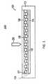
図1は、ディスプレイ10と、モバイル描画具またはスタイラス20とを備える、描画システム(概して、100として指定される)を示す。ディスプレイ10はさらに、ケーシング12と、ケーシング12の内側に配置される背面電極層14と、背面電極層14に隣接して配置される電気光学媒体13の層と、ディスプレイ媒体13に隣接して配置される保護層18とを備える。 FIG. 1 shows a drawing system (generally designated as 100) with a
保護層18は、描画表面としての役割を果たしてもよい。描画具20は、電荷伝導機構を含んでもよく、筆記デバイス(例えば、スタイラス)であってもよい。ディスプレイ10は、描画表面に対して移動されるロボットアームまたは電荷搬送印刷ヘッドを用いて機械的にアドレス指定されてもよい。例えば、外部印刷頭部が、描画表面上に描画するために使用されてもよい。道具20が描画表面に接触すると、道具20および背面電極層14は、電磁場(例えば、電場および/または磁場)をディスプレイ媒体13を横断して印加し、それによって、画像をシステム100の描画表面上に表示してもよい。 The
ケーシング12は、電気光学ディスプレイ媒体13、背面電極層14、および/または任意の必要電子機器を保持可能なプラスチック容器(または別の材料の容器)であってもよい。ケーシング12は、玩具用途のための小サイズから大型のプレゼンテーションディスプレイにおける用途のための大サイズまで及ぶ任意のサイズであってもよく、モバイル描画具20および/または他の付属品を格納するためのコンパートメントを含んでもよい。 The casing 12 may be a plastic container (or a container of another material) capable of holding the electro-
電気光学材料13は、粒子ベースの電気泳動材料であってもよく、少なくとも2つの相、すなわち、電気泳動造影剤相17(すなわち、不連続相)と、コーティング/結合相16(すなわち、連続相)とを含んでもよい。電気泳動相17は、いくつかの実施形態では、クリアもしくは染色媒体中に分散される単一種の電気泳動粒子、またはクリアもしくは染色媒体中に分散される明確に異なる物理的および電気特性を有する1つを上回る種の電気泳動粒子を含む。いくつかの実施形態では、電気泳動相17は、カプセル壁19が電気泳動粒子および懸濁流体を囲繞するようにカプセル化される。電気光学材料13は、電気泳動および他の電気光学媒体に関する前述の特許ならびに出願に議論される先行技術タイプのいずれかであってもよい。 The electro-
描画具20は、例えば、道具20とディスプレイ10との間で電気信号を搬送するように構成される1つまたはそれを上回るワイヤによって、ディスプレイ10に機械的に結合されてもよい。ディスプレイ10は、道具20のための電源を提供してもよい。代替として、道具20は、ワイヤレス(すなわち、道具20は任意のワイヤによってディスプレイ10に結合されなくてもよい)であってもよく、その独自の電源を含んでもよい。 The
図2は、微細な線の描画を可能にするために小さくてもよく、かつ丸みを帯びていてもよい先端24を伴う、伸長プローブ22を備える、描画具20a(例えば、スタイラス)を通した概略断面を示す。先端24は、先端24の表面と同一平面またはそれに隣接する、電極26を含んでもよい。電極26は、先端24より小さい面積を包含してもよく、1つまたはそれを上回るワイヤ21を通して電圧源(図示せず)に接続されてもよい。道具20aの丸みを帯びた先端は、道具20aのより広い面積が描画表面に接触することを可能にする一方、描画表面を貫通せずに、微細な線が描写されることを可能にする。電極26は、誘電コーティング(図示せず)で被覆され、これは、道具20aを保護し、環境への電極26の暴露を防止する。道具20aの先端24は、エラストマー材料を備えてもよい。 FIG. 2 is passed through a drawing tool 20a (eg, a stylus) comprising an extension probe 22 with a
本装置において使用される描画具またはスタイラスは、その先端の中に内蔵された制振機構(例えば、ばね)を含み、描画表面を物理的力(例えば、ユーザの手の運動によって生じる物理的力)から和らげてもよい。 The drawing tool or stylus used in this device includes a vibration damping mechanism (for example, a spring) built in the tip of the drawing tool or stylus, and physically forces the drawing surface (for example, a physical force generated by the movement of the user's hand). ) May be relieved.
図3Aは、背面電極層314と、ディスプレイ媒体316とを備える、ディスプレイユニット310を通した断面である。ディスプレイ媒体316は、描画表面341と背面電極層314との間に介在される。背面電極層314は、2つまたはそれを上回る電極(例えば、第1の電極332および第2の電極334)を含んでもよい。2つまたはそれを上回る電極の電位は、独立して制御されてもよく、これは、例えば、本明細書に説明されるように、フリンジ電場を生成するために有益であり得る。 FIG. 3A is a cross section of the
ディスプレイ媒体316は、複数のカプセル342を備える、電気泳動ディスプレイ媒体であってもよい。図3Aでは、各カプセル342は、実質的にクリアな懸濁流体中に懸濁された異なる(例えば、造影)光学特性を伴う、第1および第2のタイプの粒子を含むが、これは、限定ではなく、ディスプレイ媒体316のカプセルは、任意の好適な懸濁流体中に懸濁された任意の好適な数の粒子タイプを含んでもよい。 The
ディスプレイユニット310は、ディスプレイ媒体316に隣接して配置される、保護層318を含んでもよい。保護層318の表面は、描画システムのための描画表面341としての役割を果たしてもよい。好適な保護層は、図1を参照して前述されている。ディスプレイユニット310のいくつかの変形は、ディスプレイ媒体316の描画表面側(「正面」)上に電極を含まなくてもよい。代わりに、ディスプレイ媒体316は、モバイル描画具によって外部からアドレス指定されてもよい。 The
ディスプレイユニット310は、背面電極層314内の電極の電位を制御することによって、ディスプレイユニット310の動作を制御し得る、ディスプレイコントローラ(例えば、制御回路)(図示せず)を含んでもよい。ディスプレイコントローラは、図1を参照して前述のように、電荷発生機構(図示せず)によって背面電極層314への電荷の印加を制御することによって、背面電極層314内の電極の電位を制御してもよい。ディスプレイコントローラは、任意の好適な処理デバイス(例えば、マイクロコントローラ、マイクロプロセッサ、特定用途向け集積回路等)を使用して実装されてもよい。ディスプレイコントローラは、ディスプレイユニット310を「描画モード」または「消去モード」で動作するように選択的に構成してもよい。ディスプレイコントローラは、背面電極層314の電極を同一電位(例えば、電気接地)に設定し、それによって、描画具が描画具の電極を異なる電位に設定することによりディスプレイ媒体316を外部からアドレス指定することを可能にすることによって、ディスプレイユニット310を「描画モード」で動作するように構成してもよい。ディスプレイコントローラは、背面電極層314の電極を異なる電位に設定することによって(例えば、AC電圧を電極層314の電極を横断して印加することによって)、描画ユニット310を「消去モード」で動作するように構成してもよい。ユーザは、任意の好適な技法(例えば、ディスプレイコントローラに通信可能に結合されるボタンを押下する、ディスプレイコントローラに通信可能に結合されるスイッチをアクティブ化する、音声コマンドを発する、ソフトウェアベースのユーザインターフェースを動作させる等)を使用して入力をディスプレイコントローラに提供することによって、描画システムの動作モードを制御してもよい。描画および消去モードは、以下でさらに詳細に議論される。 The
図3Bは、ディスプレイユニット310と、描画具320とを含む、ディスプレイシステム300を通した断面を示す。描画具は、スタイラスであってもよい。描画具の先端の幅366は、カプセル342の幅346の少なくとも2倍であってもよい。代替として、描画具320は、印刷ヘッドまたはその一部であってもよい。モバイル描画具のいくつかの実施形態は、図2を参照して前述されている。 FIG. 3B shows a cross section through the
道具320は、電位352に設定され得る、電極(図示せず)を含んでもよい。電位352が背面電極層314内の対向電極の電位と異なるとき、電場が、道具320と背面電極層314との間に配置される1つまたはそれを上回るカプセル342に印加され、それによって、1つまたはそれを上回るカプセルを対応する光学状態に駆動する。
図3Bは、背面電極層314の電極が接地される(図3Bでは、ゼロで示される)、描画モードで動作する描画システム300を図示する。背面電極層314の電極の接地は、描画モードに必須ではないが、背面電極層314の電極を面積全体を通して共通電位に設定することは、その面積全体を通して描画システムの光学特性の均一性を向上させ得る。例えば、背面電極層314の電極が、共通電位に設定され、道具320が、ディスプレイ媒体を外部からアドレス指定するために使用されるとき、描画システム300によって表示されるマーキングは、十分に均一な色であり得る。共通電位は、限定ではないが、電気接地を含む、任意の好適な電位であってもよい。 FIG. 3B illustrates a
描画モードでは、道具320の電極は、電位352に維持されてもよい。道具320の先端が、ディスプレイ媒体316に近接して(例えば、描画表面341と接触して)設置されると、背面電極層314と描画具の電極との間の電圧差が、描画具の先端に隣接するカプセル342を通して電場を背面電極層314と描画具の電極との間に形成させるであろう。本電場は、これらのカプセルの内容物を対応する光学状態(例えば、色)に駆動させてもよい。ディスプレイ媒体316が双安定(または多安定)であるため、これらのカプセルは、電場が除去された後も(例えば、描画具320の先端がカプセルから離れて移動された後も)、その光学状態を留保する。 In drawing mode, the electrodes of
図3Bでは、描画具320の電極は、正電位352に荷電され、描画具の電極と背面電極層314との間に形成される電場は、白色の負に荷電された粒子をカプセルの上部に伴い、黒色の正に荷電された粒子をこれらのカプセルの底部に伴って、カプセル342b−342dを白色状態に駆動する。描画具320によってアドレス指定されないカプセル342aおよび342e−gは、グレー状態に留まり、白色および黒色粒子は、各カプセル全体を通して均一に分散される。 In FIG. 3B, the electrodes of the
図3Bに示される光学状態および電位は、非限定的実施例である。カプセル342は、カプセルのグレー状態の色が灰色であるように、実質的にクリアな懸濁流体中に分散されるほぼ等量の黒色および白色インク粒子を含んでもよい。代替として、カプセル342は、カプセルのグレー状態の色が実質的に白色であるように、黒色インク粒子より多くの白色インク粒子を含んでもよい。描画具320の電極は、背面電極層314に対して正または負電位に荷電され、それぞれ、描画具の先端の近傍におけるカプセルを白色または黒色状態に駆動してもよい。したがって、描画システム300は、例えば、ユーザが、カプセル342の組成物ならびに描画具320および背面電極層314の相対的電位に応じて、灰色上黒色、灰色上白色、または白色上黒色を描画することを可能にしてもよい。 The optical states and potentials shown in FIG. 3B are non-limiting examples.
道具320は、描画具の電極の電位を制御することによって描画具320の動作を制御し得る、道具コントローラ(例えば、制御回路)(図示せず)を含んでもよい。道具コントローラは、電荷発生機構(図示せず)によって電極の電荷の印加を制御することによって、描画具の電極の電位を制御してもよい。電荷発生機構のいくつかの実施形態は、前述の通りである。道具コントローラは、任意の好適な処理デバイス(例えば、マイクロコントローラ、マイクロプロセッサ、特定用途向け集積回路等)を使用して実装されてもよい。 The
道具コントローラは、第1の光学状態(例えば、第1の色)または第2の光学状態(例えば、第2の色)で描画するように描画具320を選択的に構成してもよい。道具コントローラは、描画具の電極を背面電極層314に対して負電位に設定することによって第1の光学状態で、描画具の電極を背面電極層314に対して正電位に設定することによって第2の光学状態で描画するように描画具320を構成してもよい。ユーザは、任意の好適な技法を使用して(例えば、道具コントローラに通信可能に結合されるボタンを押下する、道具コントローラに通信可能に結合されるスイッチをアクティブ化する、音声コマンドを発する、ソフトウェアベースのユーザインターフェースを動作させる等)、入力を道具コントローラに提供することによって描画具の動作を制御してもよい。 The tool controller may selectively configure the
図3Cは、消去モードにおける第2の状態にある描画ユニット310を通した断面を示す。消去モードでは、電圧(「消去電圧」)が、背面電極層314の隣接する電極間に確立され、それによって、電場を電極間に形成させてもよい。得られたフリンジ電場は、カプセル342を透過し、それらをグレー状態に駆動する。フリンジ電場は、電気浸透流をカプセル342内に誘発し得、これは、カプセル内の粒子を「旋回」させ得る(例えば、ランダムに混合させる)。粒子の旋回は、カプセルをグレー状態に迅速かつ効率的に駆動し得る。ディスプレイ媒体316を効率的に消去するために好適な「消去電圧」のいくつかの実施形態および電極層314の構成は、以下に説明される。 FIG. 3C shows a cross section through the
ディスプレイ媒体316(またはその一部)は、ディスプレイ媒体の同一側上の電極(例えば、背面電極層314内の電極332および334)を横断して「消去電圧」を確立することによって消去されてもよい。消去電圧を確立するために電極に印加される電位は、同一極性または反対極性を有してもよい。図3Cでは、電極332および334に印加される電位は、それぞれ、「+」および「−」記号によって示されるように、反対極性を有する。消去電圧の振幅は、典型的には、10〜240ボルト、好ましくは、10〜120ボルトであってもよい。消去電圧は、AC電圧であってもよく、これは、1〜1000Hz(例えば、10〜100Hzまたは10〜60Hz)の周波数を有してもよい。代替として、消去電圧は、DC電圧であってもよい。しかしながら、AC消去電圧は、ディスプレイ媒体の消去される部分を横断してより均一な光学状態を産生する傾向にあり得る一方、DC消去電圧は、ディスプレイ媒体の消去される部分を横断してより細いストライプを産生する傾向にあり得る。 Even if the display medium 316 (or a portion thereof) is erased by establishing an "erasing voltage" across electrodes on the same side of the display medium (eg,
消去電圧の印加によって誘発される粒子の旋回は、電気泳動粒子をランダムに混合させ得る。カプセルの電気泳動粒子をランダムに混合させることによって、消去電圧は、カプセルの前の光学状態にかかわらず、カプセルをグレー状態に駆動し得、したがって、要求される消去電圧は、カプセルの前の光学状態に依存しない。また、消去電圧がディスプレイ媒体316に隣接する電極に印加されると、ディスプレイ媒体のその部分の好適な消去が、いくつかの実施形態では、比較的に短い時間期間(例えば、1秒未満)にわたって消去電圧を印加することによって達成され得る。 The particle swirl induced by the application of the erasing voltage can randomly mix the electrophoretic particles. By randomly mixing the electrophoretic particles of the capsule, the erasing voltage can drive the capsule to a gray state regardless of the optical state in front of the capsule, so the required erasing voltage is the optics in front of the capsule. State independent. Also, when an erasing voltage is applied to the electrodes adjacent to the
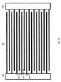
電極層314の電極は、互いに組み合わせられ、消去を促進してもよい。図3Dは、互いに組み合わせられた電極332および334を伴う、背面電極層314の上部平面図である。互いに組み合わせられた電極の桁間間隙379、桁幅377、およびピッチ375は、少なくとも部分的に、カプセル342の幅346(「インク幅」)および厚さ348(「インク厚さ」)に基づいて判定されてもよい。インク幅346の公称値は、50ミクロンであってもよく、インク厚さ348の公称値は、20ミクロンであってもよい。 The electrodes of the
互いに組み合わせられた電極は、任意の好適な寸法を有してもよいが、消去モードにおける性能を向上させるいくつかの電極構成が、描画モードにおける性能を妨害し得、その逆も同様であることが経験的に観察されている。例えば、描画モードでは、性能は、互いに組み合わせられた電極の桁間の桁間間隙379が可能な限り小さいとき、均一電位に設定される電極層314の面積の増加が描画システムの外部アドレス指定の分解能を改良し得るため、向上され得る。同様に、外部アドレス指定の分解能は、互いに組み合わせられた電極の各伸長部分の幅377がカプセルの幅346とほぼ等しいときと、各カプセル342が伸長部分の上部に心合されるとき、描画モードにおいて向上され得る。対照的に、消去モードでは、性能は、互いに組み合わせられた電極の桁間間隙379および桁幅377の両方が、インクカプセルの厚さ348とインクカプセルの幅346の2倍との間にあるとき、これらの構成が、フリンジ電場を産生させ、これが電気泳動粒子をより均一に混合させ得るため、向上され得る。 The electrodes combined with each other may have any suitable dimensions, but some electrode configurations that improve performance in erase mode may interfere with performance in drawing mode and vice versa. Has been empirically observed. For example, in drawing mode, the performance is that when the
描画モードおよび消去モードの両方において好適な性能を提供する、電極構成(例えば、外部アドレス指定のための好適な分解能および消去されるカプセル間の好適な均一性を提供する、電極構成)が、識別されている。互いに組み合わせられた電極の桁間間隙379、桁幅377、およびピッチ375は、それぞれ、インク幅346の半分(例えば、25ミクロン)、インク幅346の半分(例えば、25ミクロン)、およびインク幅(例えば、50ミクロン)に等しくてもよい。 Electrode configurations that provide suitable performance in both draw and erase modes (eg, electrode configurations that provide good resolution for external addressing and good uniformity between erased capsules) identify. Has been done. The
図3Dにおける背面電極層314は、ディスプレイ媒体316全体の下にある、単一の対の互いに組み合わせられた電極を含むが、これは、必須ではなく、背面電極層314の電極は、電極を好適な電位に設定することがディスプレイ媒体316のカプセルを消去するために好適なフリンジ電場を発生させるように、任意の好適なパターンで構成されてもよい。背面電極層314の電極は、互いに組み合わせられなくてもよい。電極は、電極への好適な電位の印加が、ディスプレイ媒体316を消去し、パターンをディスプレイ媒体316上に形成させるように構成されてもよい(例えば、罫線付きの紙のシート上の線が判読可能な筆記を促進する様式に類似する、ディスプレイ媒体上での判読可能な筆記を促進するための線のパターン)。 The
背面電極層は、ディスプレイ媒体316の対応する領域の消去を制御するように構成される、2つまたはそれを上回る電極のセットを含んでもよい。領域別消去動作では、消去電圧が、1つの電極のセットに印加され、ディスプレイ媒体316の対応する領域を消去してもよい一方、領域間消去動作では、消去電圧が、2つまたはそれを上回る電極のセットに印加され、ディスプレイ媒体316の対応する領域を消去してもよく、大域的消去動作では、消去電圧が、電極の全セットに印加され、ディスプレイ媒体316の全領域を消去してもよい。これらの動作は、ディスプレイコントローラを通してユーザによって制御されてもよい。 The back electrode layer may include a set of two or more electrodes configured to control the erasure of the corresponding region of the
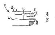
図4Aおよび4Bは、それぞれ、相互から絶縁される2つまたはそれを上回る電極26を含む、描画具20bの概略断面および下面平面図である。1つまたはそれを上回る電圧が、電極26の全部または一部に印加され、描画具によってディスプレイデバイス上に描画される線の幅および/または形状を制御してもよい。例えば、電磁場が電極26aのみを通して印加されると、細い線が、描画表面上に描画されてもよい。しかしながら、電磁場が電極26aおよび26bの両方を通して印加されると、より太い線が、描画されてもよく、さらに太い線が、電磁場が3つの電極26a、26b、および26cを通して印加されると、描画されてもよい。描画される線の幅は、ディスプレイ媒体を横断して印加された電圧を変動させること以外によって制御されてもよい。例えば、印加される電圧のデューティサイクルもしくは大きさおよび/または持続時間が、変動されることができる。 4A and 4B are schematic cross-sectional and bottom plan views of the
描画具20bは、電極26の電位を制御することによって、描画具20bの動作を制御し得る、道具コントローラ(例えば、制御回路)27を含んでもよい。コントローラ27は、前述のように、電荷発生機構(図示せず)によって電極への電荷の印加を制御することによって、電極26の電位を制御してもよい。コントローラ27は、任意の好適な処理デバイス(例えば、マイクロコントローラ、マイクロプロセッサ、特定用途向け集積回路等)を使用してもよい。 The
コントローラ27は、第1の光学状態(例えば、第1の色)または第2の光学状態(例えば、第2の色)で描画するように描画具20bを選択的に構成してもよい。コントローラは、電極26を描画システムの背面電極層に対して負電位に設定することによって第1の光学状態で描画し、電極26を描画システムの背面電極層に対して正電位に設定することによって第2の光学状態で描画するように描画具20bを構成してもよい。ユーザは、任意の好適な技法を使用して(例えば、道具コントローラに通信可能に結合されるボタンを押下する、道具コントローラに通信可能に結合されるスイッチ25をアクティブ化する、音声コマンドを発する、ソフトウェアベースのユーザインターフェースを動作させる等)、入力を道具コントローラに提供することによって描画具の動作を制御してもよい。 The controller 27 may selectively configure the
図5Aは、ディスプレイユニット510がモバイル描画具520によって印加されたフリンジ電場によって消去され得る、第1の状態における描画システム500を通した断面である。描画システム500は、多くの点において描画システム300に類似し得る。例えば、描画システム500は、ディスプレイデバイス510と、モバイル描画具520とを含んでもよい。ディスプレイデバイス510は、背面電極層514と、保護層518と、背面電極層と保護層との間に配置されるディスプレイ媒体516とを含んでもよい。ディスプレイ媒体516は、複数のカプセル542を含み得る、電気泳動ディスプレイ媒体を備えてもよい。保護層518の1つの表面は、描画表面541としての役割を果たしてもよい。ディスプレイデバイス510は、背面電極層514の電位を制御し得る(例えば、電荷発生機構によって背面電極層514への電荷の印加を制御することによって)、ディスプレイコントローラ(例えば、制御回路)(図示せず)を含んでもよい。 FIG. 5A is a cross section of the
しかしながら、描画システム500は、いくつかの点において描画システム300と異なる。背面電極層514は、ディスプレイ媒体516の下にある単一電極(例えば、プレート電極)を備えてもよい。しかしながら、これは、必須ではなく、背面電極層514は、任意の好適な数および/または構成の電極を備えてもよい。ディスプレイコントローラは、背面電極層514の電極を一定電位(例えば、電気接地)に設定するように構成されてもよい。ディスプレイ媒体516は、2つまたはそれを上回る電極562と、電極562の電位を制御することによって道具520の動作を制御するように構成される、道具コントローラ(例えば、制御回路)(図示せず)とを含み得る、モバイル描画具520によって、外部からアドレス指定されてもよい。コントローラは、2つもしくはそれを上回る光学状態(例えば、色)のうちの1つで描画する、またはディスプレイ媒体516の一部を消去するように描画具520を選択的に構成してもよい。 However, the
電極562の電位552が、背面電極層514の電位と異なるとき、電場が、描画具520と背面電極層514との間に配置される1つまたはそれを上回るカプセル542に印加され、それによって、1つまたはそれを上回るカプセルを対応する光学状態に駆動するであろう。したがって、コントローラは、1つまたはそれを上回る電極562を背面電極層514に対して正電位に設定し、残りの電極562が電気的に浮動状態または背面電極層514と同一電位に設定されることによって、第1の光学状態(例えば、色)で描画するように描画具520を制御してもよい。代替として、コントローラは、1つまたはそれを上回る電極562を背面電極層514に対して負電位に設定し、任意の残りの電極562が電気的に浮動状態または背面電極層514と同一電位に設定されることによって、第2の光学状態(例えば、色)で描画するように道具520を制御してもよい。 When the potential 552 of the electrode 562 is different from the potential of the
図5Aは、ディスプレイ媒体516上で描画するために使用される道具520と、接地された背面電極層514と、背面電極層の電位に対して正電位に設定される電極562とともに、「描画モード」で動作する描画システム500を示す。したがって、道具520によってアドレス指定されるカプセルは、グレー状態から白色状態に駆動される。 FIG. 5A shows a “drawing mode” with a
図5Aに示される光学状態および電位は、限定ではない。前述のように、道具520がディスプレイ媒体を駆動する光学状態は、道具520と背面電極層514との間の電圧と、カプセル542の内容物(例えば、電気泳動粒子および懸濁流体の光学特性ならびに相対的量)とに依存する。背面電極層514は、描画モードでは、限定ではないが、電気接地を含む、任意の好適な電位に設定されてもよく、1つまたはそれを上回る電極562が、描画モードでは、限定ではないが、背面電極層514の電位を上回る第1の電位または背面電極層514の電位未満の第2の電位を含む、任意の好適な電位に設定されてもよく、第1および第2の電位は、それぞれ、ディスプレイ媒体516の第1および第2の光学状態に対応する。 The optical states and potentials shown in FIG. 5A are not limited. As mentioned above, the optical state in which the
図5Bは、消去モードで動作する描画システム500を通した断面を示す。消去モードでは、1つまたはそれを上回る電圧(「消去電圧」)が、道具520の隣接する電極間に確立され、それによって、電場と関連付けられたフリンジ電場が描画具の先端に隣接するカプセル542に透過し、それらのカプセルをグレー状態に駆動し(例えば、カプセルの内容物を旋回させることによって)、それによって、描画具の先端に対して局所的な面積内のカプセルを消去するように、これらの電場を電極間に形成させてもよい。ディスプレイ媒体516を消去するために好適な描画具の電極の「消去電圧」および構成は、以下に説明される。 FIG. 5B shows a cross section through a
道具520の先端に隣接するディスプレイ媒体516の一部は、道具520の電極を横断して「消去電圧」を確立することによって消去されてもよい。消去電圧を確立するために電極に印加される電位は、同一極性、または図5Bに示されるように、反対極性を有してもよい。消去電圧の大きさは、典型的には、10〜240ボルト、好ましくは、10〜120ボルトであってもよい。消去電圧は、AC電圧であってもよく、1〜1000Hz(例えば、10〜100Hzまたは10〜60Hz)の周波数を有してもよい。代替として、消去電圧は、DC電圧であってもよい。描画具の先端に隣接するディスプレイ媒体の部分の好適な消去は、比較的に短い時間期間(例えば、1秒)にわたって消去電圧を描画具の電極に印加することによって達成され得る。 A portion of the display medium 516 adjacent to the tip of the
好適な電極構成に関して、描画システム300の背面電極層314内で電極に適用される同一考慮点はまた、描画具520の電極562にも適用可能である。描画具の先端内の隣接する電極562間の間隙579、電極562の幅577、および電極562のピッチ575は、少なくとも部分的に、カプセル542の幅(「インク幅」)および厚さ(「インク厚さ」)に基づいて判定されてもよい。電極間間隙579、電極幅577、および電極ピッチ575は、それぞれ、例えば、インク幅の半分(例えば、25ミクロン)、インク幅の半分(例えば、25ミクロン)、およびインク幅(例えば、50ミクロン)に等しくてもよい。道具520の電極は、電極をディスプレイ媒体516のカプセルを消去するために好適なフリンジ電場を発生させるために好適な電位に設定するように、任意の好適なパターンで構成されてもよい。電極562は、図4Aおよび4Bに示されるように、同心円形で配列されてもよい。 With respect to the preferred electrode configuration, the same considerations that apply to the electrodes within the
道具コントローラは、道具520を制御し、消去電圧を道具の電極の2つまたはそれを上回るものの間に確立することによって、道具の先端に隣接する1つまたはそれを上回るカプセルを消去してもよい。道具520内の任意の残りの電極562は、電気的に浮動状態または背面電極層514と同一電位に設定されてもよい。 The tool controller may erase one or more capsules adjacent to the tip of the tool by controlling the
図5Bでは、背面電極層514は、接地され、消去電圧は、道具520の電極562aと562bとの間に確立される。描画具の電極間の電圧は、電場を電極間に形成させ、フリンジ電場は、カプセル542b−dを透過し、それによって、カプセル542b−dを消去する。図5Bに示される光学状態および電位は、非限定である。 In FIG. 5B, the
描画システム300および描画システム500の側面は、組み合わせられてもよい。例えば、描画システムは、ディスプレイ媒体の領域別、領域間、および/または大域的消去を行うように構成可能な2つまたはそれを上回る電極を伴う、背面電極層314と、ディスプレイ媒体上で描画し、および/またはディスプレイ媒体の局所的消去を行うように構成される、描画具520とを含んでもよい。 The aspects of the
本発明は、カラー描画システム(例えば、3つもしくはそれを上回る色で描画するための描画システム、および/または黒色、白色、もしくは灰色以外の少なくとも1つの色で描画するための描画システム)に適用されることができる。そのようなカラー描画システムは、カラーディスプレイ媒体の領域別、領域間、および/または大域的消去を行うように構成可能な2つもしくはそれを上回る電極を伴う背面電極層を有する、カラーディスプレイユニットを含んでもよい。大域的消去(または領域別もしくは領域間消去)は、色を選択し、ディスプレイユニット上で描画することに先立って、カラーディスプレイユニット(またはその一部)を中間光学状態にリセットするために行われてもよい。カラー描画システムは、ディスプレイ媒体上で描画する(例えば、3つもしくはそれを上回る色、および/または黒色、白色、もしくは灰色以外の少なくとも1つの色で)、および/またはディスプレイ媒体の局所的消去を行うように構成可能な描画具を含んでもよい。カラーディスプレイのために好適な描画具は、電磁場を使用して、異なる電気電荷および/または異なる磁気特性を有し得る、異なる色の粒子を制御してもよい。 The present invention applies to color drawing systems (eg, drawing systems for drawing in three or more colors and / or drawing systems for drawing in at least one color other than black, white, or gray). Can be done. Such a color drawing system comprises a color display unit having a back electrode layer with two or more electrodes that can be configured to perform regional, interregional, and / or global erasure of the color display medium. It may be included. Global erasure (or region-by-region or inter-regional erasure) is performed to reset the color display unit (or part of it) to an intermediate optical state prior to selecting a color and drawing on the display unit. You may. The color drawing system draws on the display medium (eg, with three or more colors and / or at least one color other than black, white, or gray) and / or local erasure of the display medium. It may include drawing tools that can be configured to do so. Suitable drawing tools for color displays may use electromagnetic fields to control particles of different colors that may have different electrical charges and / or different magnetic properties.
図6Aは、カラー描画システム(概して、600として指定される)を通した断面である。カラー描画システムの電気泳動ディスプレイ媒体のカプセルは、3つまたはそれを上回る異なるタイプの顔料粒子を含有してもよい。図6Aでは、各カプセルは、1、2、および3として指定される、3つの異なるタイプの顔料粒子を含む。異なるタイプの顔料粒子は、光学的に相互に異なってもよい。例えば、粒子は、反射または透過性であってもよく、白色、黒色、または有色であってもよい。全3つの顔料タイプは、散乱してもよい。これらの異なるタイプの顔料粒子はまた、異なる電気泳動応答を有してもよい。例えば、粒子は、異なるタイプの粒子が電磁場に異なるように応答するように、正に荷電される、負に荷電される、荷電されない、および/または磁性であってもよい。粒子1、2、および3は、透過性顔料粒子であってもよく、粒子1および2は、反対に荷電されてもよく、粒子3は、荷電されず、強磁性または超常磁性であってもよい。例えば、顔料粒子1は、白色であって、負に荷電されてもよく、顔料粒子2は、赤色であって、正に荷電されてもよく、顔料粒子3は、シアン色であって、強磁性または超常磁性であってもよい。 FIG. 6A is a cross section through a color drawing system (generally designated as 600). Capsules of electrophoretic display media in color drawing systems may contain three or more different types of pigment particles. In FIG. 6A, each capsule contains three different types of pigment particles designated as 1, 2, and 3. Different types of pigment particles may be optically different from each other. For example, the particles may be reflective or transparent, white, black, or colored. All three pigment types may be scattered. These different types of pigment particles may also have different electrophoretic responses. For example, the particles may be positively charged, negatively charged, uncharged, and / or magnetic so that different types of particles respond differently to the electromagnetic field. Particles 1, 2, and 3 may be permeable pigment particles, particles 1 and 2 may be charged in opposition, and particle 3 may be uncharged and ferromagnetic or superparamagnetic. Good. For example, the pigment particles 1 may be white and negatively charged, the pigment particles 2 may be red and positively charged, and the pigment particles 3 may be cyan and strongly charged. It may be magnetic or supernatural.
図6Aでは、カラー描画システム600のディスプレイユニットは、消去モードで動作しており、ディスプレイユニットのカプセル内の顔料粒子は、中間光学状態にある。カラー描画システム600のカプセルを通したフリンジ電場の印加は、カプセルの顔料粒子の旋回をもたらし得る。電気的に荷電された粒子は、電場の印加に応答して旋回を開始し得、電気的に荷電された粒子の移動によって生成される流体運動は、任意の荷電されない顔料粒子(例えば、荷電されない磁気顔料粒子)を効果的に旋回させ得る。 In FIG. 6A, the display unit of the
描画具は、電場、磁場、および/または電磁場をカラーディスプレイユニットに選択的に印加してもよい。前述のように、ユーザは、任意の好適な技法を使用して入力を描画具の道具コントローラに提供することによって、描画具の動作モードを制御してもよい。 The drawing tool may selectively apply an electric field, a magnetic field, and / or an electromagnetic field to the color display unit. As mentioned above, the user may control the operating mode of the drawing tool by providing input to the drawing tool tool controller using any suitable technique.
図6B−6Dは、3つの光学状態で動作するカラー描画システム600の断面図を示す。図6Bでは、ディスプレイユニットは、描画モードで動作しており、描画具は、磁場を以前に消去された状態であったディスプレイユニットのカプセル上に付与しており、それによって、磁気顔料粒子3をカプセルの正面表面(図示されるような上側表面)に持って来る。図6Cでは、ディスプレイユニットは、描画モードで動作しており、描画具は、正電圧を以前に消去された状態であったディスプレイユニットのカプセルを横断して生成しており、それによって、負に荷電された顔料粒子1をカプセルの正面表面に持って来る。図6Dでは、ディスプレイユニットは、描画モードで動作しており、描画具は、負電圧を以前に消去された状態であったディスプレイユニットのカプセルを横断して生成しており、それによって、正に荷電された顔料粒子2をカプセルの正面表面に持って来る。 6B-6D show a cross-sectional view of a
図6A−6Dに示される光学状態によって産生される色は、表1に示される。 The colors produced by the optical states shown in FIGS. 6A-6D are shown in Table 1.

別の類似ディスプレイでは、粒子タイプ1は、負電気電荷を伴う透過性マゼンタ色であってもよく、粒子タイプ2は、正電気電荷を伴う透過性黄色であってもよく、粒子タイプ3は、透過性シアン色および磁性であってもよい。流体は、ディスプレイユニットのカプセルの視認表面近傍の顔料粒子のみがユーザに可視となるように、十分な中立(例えば、荷電されていない、非磁性)白色粒子を含んでもよい。そのような粒子を伴うカプセルを有するカラーディスプレイは、表2に示されるようにアドレス指定され、表2に列挙される色を産生してもよい。 In another similar display, particle type 1 may be a transmissive magenta color with a negative electric charge, particle type 2 may be a transmissive yellow with a positive electric charge, and particle type 3 may be a transmissive yellow color. It may be transparent cyan and magnetic. The fluid may include sufficiently neutral (eg, uncharged, non-magnetic) white particles such that only the pigment particles near the visible surface of the capsule of the display unit are visible to the user. Color displays with capsules with such particles may be addressed as shown in Table 2 and produce the colors listed in Table 2.
Claims (16)
Translated fromJapanese電気光学ディスプレイと、
2つの独立してアドレス指定可能なスタイラス電極を含むスタイラスと
を備え、
前記電気光学ディスプレイは、
第1の極性を有する第1のセットの荷電された粒子と、前記第1の極性と反対の第2の極性を有する第2のセットの荷電された粒子と、荷電されていない第3のセットの磁性粒子とを備える電気泳動ディスプレイ媒体であって、前記第1、第2、および第3のセットの粒子は、流体内にあり、前記第1のセットの荷電された粒子および前記第2のセットの荷電された粒子は、印加された電場に応答して前記流体内を移動し、前記第3のセットの磁性粒子は、印加された磁場に応答して前記流体内を移動し、前記電気泳動ディスプレイ媒体は、前記第1のセットの荷電された粒子、前記第2のセットの荷電された粒子、および前記第3のセットの磁性粒子の色ならびにグレー色を表示することが可能である、電気泳動ディスプレイ媒体と、
前記電気泳動ディスプレイ媒体の1つの表面に隣接して配置される、互いに組み合わせられた電極であって、前記電気泳動ディスプレイ媒体の描画表面側には電極が配置されておらず、前記描画表面側は、前記互いに組み合わせられた電極と反対の前記電気泳動ディスプレイ媒体の第2の表面に隣接する、互いに組み合わせられた電極と、
前記互いに組み合わせられた電極の電位を制御するための電圧コントローラであって、前記電圧コントローラは、前記グレー色を表示するように前記電気泳動ディスプレイ媒体の少なくとも一部を駆動するフリンジ電場が前記電気泳動ディスプレイ媒体に提示されるように前記互いに組み合わせられた電極に電圧を印加することが可能である、電圧コントローラと
を含み、
前記電圧コントローラは、前記互いに組み合わせられた電極のうちの少なくとも1つと前記スタイラス電極のうちの少なくとも1つとの間の電位差を制御することにより前記電気泳動ディスプレイ媒体の一部の光学状態を改変するように構成されている、描画デバイス。An electronically erasable drawing device
Electro-optic display and
Equipped with a stylus containing two independently addressable stylus electrodes,
The electro-optical display is
A first set of charged particles having a first polarity, a second set of charged particles having a second polarity opposite to the first polarity, and an uncharged third set. An electrophoretic display medium comprising the magnetic particles of the first, second, and third sets of particles in a fluid, the first set of charged particles and the second set of particles. The set of charged particles move in the fluid in response to an applied electric field, and the third set of magnetic particles move in the fluid in response to an applied magnetic field, theelectricity. The migration display medium is capable of displaying the colors and gray colors of the first set of charged particles, the second set of charged particles, and the third set of magnetic particles. Electromagnetic display medium and
Electrodes combined with each other arranged adjacent to one surface of the electrophoresisdisplay medium, and no electrode is arranged on the drawing surface side of the electrophoresis display medium, and the drawing surface side is , And the electrodes combined with each otheradjacent to the second surface of the electrophoresis display medium opposite to the electrodes combined with each other.
A voltage controller for controlling the potentials of the electrodes combined with each other, wherein the fringe electric field driving at least a part of theelectrophoresisdisplay medium so as to display the gray color is the electrophoresis. Including a voltage controller, which is capable of applying a voltage to the electrodes combined with each other as presented on thedisplay medium.
Said voltage controller, modifying a part of the optical state of theelectrophoretic display medium by controlling the electricposition difference between at least one of the at least one said stylus electrode of said combined together electrode A drawing device that is configured to do so.
Applications Claiming Priority (2)
| Application Number | Priority Date | Filing Date | Title |
|---|---|---|---|
| US201562212469P | 2015-08-31 | 2015-08-31 | |
| US62/212,469 | 2015-08-31 |
Related Parent Applications (1)
| Application Number | Title | Priority Date | Filing Date |
|---|---|---|---|
| JP2018510742ADivisionJP6571276B2 (en) | 2015-08-31 | 2016-08-31 | Erasing drawing devices electronically |
Publications (2)
| Publication Number | Publication Date |
|---|---|
| JP2019197226A JP2019197226A (en) | 2019-11-14 |
| JP6848019B2true JP6848019B2 (en) | 2021-03-24 |
Family
ID=58104143
Family Applications (2)
| Application Number | Title | Priority Date | Filing Date |
|---|---|---|---|
| JP2018510742AActiveJP6571276B2 (en) | 2015-08-31 | 2016-08-31 | Erasing drawing devices electronically |
| JP2019136694AActiveJP6848019B2 (en) | 2015-08-31 | 2019-07-25 | Electronic erasure of drawing device |
Family Applications Before (1)
| Application Number | Title | Priority Date | Filing Date |
|---|---|---|---|
| JP2018510742AActiveJP6571276B2 (en) | 2015-08-31 | 2016-08-31 | Erasing drawing devices electronically |
Country Status (5)
| Country | Link |
|---|---|
| US (1) | US10388233B2 (en) |
| EP (1) | EP3345047A1 (en) |
| JP (2) | JP6571276B2 (en) |
| CN (1) | CN107924100B (en) |
| WO (1) | WO2017040609A1 (en) |
Families Citing this family (16)
| Publication number | Priority date | Publication date | Assignee | Title |
|---|---|---|---|---|
| US9972271B2 (en)* | 2016-05-12 | 2018-05-15 | Novatek Microelectronics Corp. | Display panel |
| US10545622B2 (en)* | 2016-05-20 | 2020-01-28 | E Ink Corporation | Magnetically-responsive display including a recording layer configured for local and global write/erase |
| CN108535930A (en)* | 2018-06-11 | 2018-09-14 | 赵力衡 | A kind of electronic ink screen and its use control method |
| EP3874317B1 (en) | 2018-10-30 | 2025-03-19 | E Ink Corporation | Electro-optic assembly |
| CN113056703B (en)* | 2018-11-30 | 2024-06-14 | 伊英克公司 | Pressure sensitive writing medium comprising electrophoretic material |
| WO2020132362A1 (en) | 2018-12-21 | 2020-06-25 | E Ink Corporation | Sub-threshold addressing and erasing in a magneto-electrophoretic writing medium |
| CN109753163B (en)* | 2019-01-10 | 2022-08-05 | 合肥京东方光电科技有限公司 | Active pen and touch system |
| NL2022504B1 (en)* | 2019-02-04 | 2020-08-19 | Elstar Dynamics Patents B V | Improved optical modulator |
| CN114174961B (en)* | 2019-08-08 | 2022-10-21 | 伊英克公司 | Stylus for addressing magnetically driven display media |
| KR102832733B1 (en)* | 2019-11-22 | 2025-07-11 | 엘지전자 주식회사 | Fabricating method for display device using semiconductor light emitting device and self-assembly device used therein |
| WO2021158744A1 (en)* | 2020-02-07 | 2021-08-12 | E Ink Corporation | Electrophoretic display layer with thin film top electrode |
| US11099451B1 (en) | 2020-07-31 | 2021-08-24 | Elstar Dynamics Patents B.V. | Light modulator, substrate comprising electrodes and smart glazing |
| US11099453B1 (en) | 2020-08-03 | 2021-08-24 | Elstar Dynamics Patents B.V. | Light modulator, light modulator method and smart glazing |
| CN112782901B (en)* | 2021-01-28 | 2024-04-02 | 福州大学 | Self-powered nonvolatile display device |
| US12007660B2 (en) | 2021-06-24 | 2024-06-11 | Elstar Dynamics Patents B.V. | Light modulator, substrate comprising electrodes and smart glazing |
| KR102853834B1 (en) | 2021-12-24 | 2025-09-01 | 엘스타 다이내믹스 페이턴츠 베슬로텐 베누트샤프 | Substrate comprising diffraction-reduced electrodes and an optical modulator |
Family Cites Families (188)
| Publication number | Priority date | Publication date | Assignee | Title |
|---|---|---|---|---|
| US4418346A (en) | 1981-05-20 | 1983-11-29 | Batchelder J Samuel | Method and apparatus for providing a dielectrophoretic display of visual information |
| US5745094A (en) | 1994-12-28 | 1998-04-28 | International Business Machines Corporation | Electrophoretic display |
| US6137467A (en) | 1995-01-03 | 2000-10-24 | Xerox Corporation | Optically sensitive electric paper |
| US7848006B2 (en) | 1995-07-20 | 2010-12-07 | E Ink Corporation | Electrophoretic displays with controlled amounts of pigment |
| US7259744B2 (en) | 1995-07-20 | 2007-08-21 | E Ink Corporation | Dielectrophoretic displays |
| US8089453B2 (en) | 1995-07-20 | 2012-01-03 | E Ink Corporation | Stylus-based addressing structures for displays |
| US7411719B2 (en) | 1995-07-20 | 2008-08-12 | E Ink Corporation | Electrophoretic medium and process for the production thereof |
| US6866760B2 (en) | 1998-08-27 | 2005-03-15 | E Ink Corporation | Electrophoretic medium and process for the production thereof |
| US7999787B2 (en) | 1995-07-20 | 2011-08-16 | E Ink Corporation | Methods for driving electrophoretic displays using dielectrophoretic forces |
| US7583251B2 (en) | 1995-07-20 | 2009-09-01 | E Ink Corporation | Dielectrophoretic displays |
| US7193625B2 (en) | 1999-04-30 | 2007-03-20 | E Ink Corporation | Methods for driving electro-optic displays, and apparatus for use therein |
| US7956841B2 (en) | 1995-07-20 | 2011-06-07 | E Ink Corporation | Stylus-based addressing structures for displays |
| US7327511B2 (en) | 2004-03-23 | 2008-02-05 | E Ink Corporation | Light modulators |
| US7167155B1 (en) | 1995-07-20 | 2007-01-23 | E Ink Corporation | Color electrophoretic displays |
| US8139050B2 (en) | 1995-07-20 | 2012-03-20 | E Ink Corporation | Addressing schemes for electronic displays |
| US5760761A (en) | 1995-12-15 | 1998-06-02 | Xerox Corporation | Highlight color twisting ball display |
| US5808783A (en) | 1996-06-27 | 1998-09-15 | Xerox Corporation | High reflectance gyricon display |
| US6055091A (en) | 1996-06-27 | 2000-04-25 | Xerox Corporation | Twisting-cylinder display |
| US5930026A (en) | 1996-10-25 | 1999-07-27 | Massachusetts Institute Of Technology | Nonemissive displays and piezoelectric power supplies therefor |
| US5777782A (en) | 1996-12-24 | 1998-07-07 | Xerox Corporation | Auxiliary optics for a twisting ball display |
| AU6004798A (en) | 1997-02-06 | 1998-08-26 | University College Dublin | Electrochromic system |
| WO1999010768A1 (en)* | 1997-08-28 | 1999-03-04 | E-Ink Corporation | Novel addressing schemes for electrophoretic displays |
| US7002728B2 (en) | 1997-08-28 | 2006-02-21 | E Ink Corporation | Electrophoretic particles, and processes for the production thereof |
| EP0924551A1 (en) | 1997-12-18 | 1999-06-23 | The Technology Partnership Public Limited Company | Method and apparatus for matrix addressing of an electrophoretic display device |
| US6054071A (en) | 1998-01-28 | 2000-04-25 | Xerox Corporation | Poled electrets for gyricon-based electric-paper displays |
| US6445489B1 (en) | 1998-03-18 | 2002-09-03 | E Ink Corporation | Electrophoretic displays and systems for addressing such displays |
| US6753999B2 (en) | 1998-03-18 | 2004-06-22 | E Ink Corporation | Electrophoretic displays in portable devices and systems for addressing such displays |
| US7075502B1 (en) | 1998-04-10 | 2006-07-11 | E Ink Corporation | Full color reflective display with multichromatic sub-pixels |
| AU3767899A (en) | 1998-04-27 | 1999-11-16 | E-Ink Corporation | Shutter mode microencapsulated electrophoretic display |
| WO1999059101A2 (en) | 1998-05-12 | 1999-11-18 | E-Ink Corporation | Microencapsulated electrophoretic electrostatically-addressed media for drawing device applications |
| US6241921B1 (en) | 1998-05-15 | 2001-06-05 | Massachusetts Institute Of Technology | Heterogeneous display elements and methods for their fabrication |
| US20030102858A1 (en) | 1998-07-08 | 2003-06-05 | E Ink Corporation | Method and apparatus for determining properties of an electrophoretic display |
| ATE228681T1 (en) | 1998-07-08 | 2002-12-15 | E Ink Corp | METHOD AND DEVICE FOR MEASURING THE STATE OF AN ELECTROPHORETIC DISPLAY DEVICE |
| US6184856B1 (en) | 1998-09-16 | 2001-02-06 | International Business Machines Corporation | Transmissive electrophoretic display with laterally adjacent color cells |
| US6271823B1 (en) | 1998-09-16 | 2001-08-07 | International Business Machines Corporation | Reflective electrophoretic display with laterally adjacent color cells using a reflective panel |
| US6144361A (en) | 1998-09-16 | 2000-11-07 | International Business Machines Corporation | Transmissive electrophoretic display with vertical electrodes |
| US6225971B1 (en) | 1998-09-16 | 2001-05-01 | International Business Machines Corporation | Reflective electrophoretic display with laterally adjacent color cells using an absorbing panel |
| US6128124A (en) | 1998-10-16 | 2000-10-03 | Xerox Corporation | Additive color electric paper without registration or alignment of individual elements |
| US6097531A (en) | 1998-11-25 | 2000-08-01 | Xerox Corporation | Method of making uniformly magnetized elements for a gyricon display |
| US6147791A (en) | 1998-11-25 | 2000-11-14 | Xerox Corporation | Gyricon displays utilizing rotating elements and magnetic latching |
| US7012600B2 (en) | 1999-04-30 | 2006-03-14 | E Ink Corporation | Methods for driving bistable electro-optic displays, and apparatus for use therein |
| US7119772B2 (en) | 1999-04-30 | 2006-10-10 | E Ink Corporation | Methods for driving bistable electro-optic displays, and apparatus for use therein |
| US6531997B1 (en) | 1999-04-30 | 2003-03-11 | E Ink Corporation | Methods for addressing electrophoretic displays |
| US6504524B1 (en) | 2000-03-08 | 2003-01-07 | E Ink Corporation | Addressing methods for displays having zero time-average field |
| US8009348B2 (en) | 1999-05-03 | 2011-08-30 | E Ink Corporation | Machine-readable displays |
| EP1500969A1 (en) | 1999-10-11 | 2005-01-26 | University College Dublin | Compound and its use in electrochromic devices |
| US6816146B2 (en)* | 1999-12-21 | 2004-11-09 | Ricoh Company Limited | Electrophoretic display liquid and electrophoretic display medium and device using the liquid having predetermined different volume medium particle diameters |
| US7715088B2 (en) | 2000-03-03 | 2010-05-11 | Sipix Imaging, Inc. | Electrophoretic display |
| JP2004522179A (en) | 2000-11-29 | 2004-07-22 | イー−インク コーポレイション | Addressing scheme for electronic displays |
| US6970154B2 (en) | 2001-01-11 | 2005-11-29 | Jpmorgan Chase Bank | Fringe-field filter for addressable displays |
| AU2002250304A1 (en) | 2001-03-13 | 2002-09-24 | E Ink Corporation | Apparatus for displaying drawings |
| KR100824249B1 (en) | 2001-04-02 | 2008-04-24 | 이 잉크 코포레이션 | Electrophoretic display including electrophoretic media with improved image stability |
| US20020188053A1 (en) | 2001-06-04 | 2002-12-12 | Sipix Imaging, Inc. | Composition and process for the sealing of microcups in roll-to-roll display manufacturing |
| US6982178B2 (en) | 2002-06-10 | 2006-01-03 | E Ink Corporation | Components and methods for use in electro-optic displays |
| US7535624B2 (en) | 2001-07-09 | 2009-05-19 | E Ink Corporation | Electro-optic display and materials for use therein |
| US7038670B2 (en) | 2002-08-16 | 2006-05-02 | Sipix Imaging, Inc. | Electrophoretic display with dual mode switching |
| US6825970B2 (en) | 2001-09-14 | 2004-11-30 | E Ink Corporation | Methods for addressing electro-optic materials |
| US6850230B1 (en) | 2001-10-16 | 2005-02-01 | Hewlett-Packard Development Company, L.P. | Electronic writing and erasing pencil |
| US8593396B2 (en) | 2001-11-20 | 2013-11-26 | E Ink Corporation | Methods and apparatus for driving electro-optic displays |
| US8125501B2 (en) | 2001-11-20 | 2012-02-28 | E Ink Corporation | Voltage modulated driver circuits for electro-optic displays |
| US8558783B2 (en) | 2001-11-20 | 2013-10-15 | E Ink Corporation | Electro-optic displays with reduced remnant voltage |
| US9412314B2 (en) | 2001-11-20 | 2016-08-09 | E Ink Corporation | Methods for driving electro-optic displays |
| US7528822B2 (en) | 2001-11-20 | 2009-05-05 | E Ink Corporation | Methods for driving electro-optic displays |
| US7952557B2 (en) | 2001-11-20 | 2011-05-31 | E Ink Corporation | Methods and apparatus for driving electro-optic displays |
| US7202847B2 (en) | 2002-06-28 | 2007-04-10 | E Ink Corporation | Voltage modulated driver circuits for electro-optic displays |
| US6865010B2 (en) | 2001-12-13 | 2005-03-08 | E Ink Corporation | Electrophoretic electronic displays with low-index films |
| US6900851B2 (en) | 2002-02-08 | 2005-05-31 | E Ink Corporation | Electro-optic displays and optical systems for addressing such displays |
| CN100339757C (en) | 2002-03-06 | 2007-09-26 | 株式会社普利司通 | Image displaying apparatus and method |
| US6950220B2 (en) | 2002-03-18 | 2005-09-27 | E Ink Corporation | Electro-optic displays, and methods for driving same |
| US7116318B2 (en) | 2002-04-24 | 2006-10-03 | E Ink Corporation | Backplanes for display applications, and components for use therein |
| US7649674B2 (en) | 2002-06-10 | 2010-01-19 | E Ink Corporation | Electro-optic display with edge seal |
| US20080024482A1 (en) | 2002-06-13 | 2008-01-31 | E Ink Corporation | Methods for driving electro-optic displays |
| US20110199671A1 (en) | 2002-06-13 | 2011-08-18 | E Ink Corporation | Methods for driving electrophoretic displays using dielectrophoretic forces |
| US7839564B2 (en) | 2002-09-03 | 2010-11-23 | E Ink Corporation | Components and methods for use in electro-optic displays |
| US20130063333A1 (en) | 2002-10-16 | 2013-03-14 | E Ink Corporation | Electrophoretic displays |
| TWI229230B (en) | 2002-10-31 | 2005-03-11 | Sipix Imaging Inc | An improved electrophoretic display and novel process for its manufacture |
| KR100937613B1 (en) | 2002-12-16 | 2010-01-20 | 이 잉크 코포레이션 | Backplanes for Electro-Optical Displays |
| US6922276B2 (en) | 2002-12-23 | 2005-07-26 | E Ink Corporation | Flexible electro-optic displays |
| US6831771B2 (en) | 2003-01-08 | 2004-12-14 | Sipix Imaging Inc. | Electronic whiteboard using electrophoretic display |
| TWI337679B (en) | 2003-02-04 | 2011-02-21 | Sipix Imaging Inc | Novel compositions and assembly process for liquid crystal display |
| US7339715B2 (en) | 2003-03-25 | 2008-03-04 | E Ink Corporation | Processes for the production of electrophoretic displays |
| WO2004090626A1 (en) | 2003-04-02 | 2004-10-21 | Bridgestone Corporation | Particle used for image display medium, image display panel using same, and image display |
| US20040246562A1 (en) | 2003-05-16 | 2004-12-09 | Sipix Imaging, Inc. | Passive matrix electrophoretic display driving scheme |
| JP2004356206A (en) | 2003-05-27 | 2004-12-16 | Fuji Photo Film Co Ltd | Laminated structure and its manufacturing method |
| US8174490B2 (en) | 2003-06-30 | 2012-05-08 | E Ink Corporation | Methods for driving electrophoretic displays |
| EP1656658A4 (en) | 2003-08-19 | 2009-12-30 | E Ink Corp | Methods for controlling electro-optic displays |
| WO2005029458A1 (en) | 2003-09-19 | 2005-03-31 | E Ink Corporation | Methods for reducing edge effects in electro-optic displays |
| JP2007507737A (en) | 2003-10-03 | 2007-03-29 | コーニンクレッカ フィリップス エレクトロニクス エヌ ヴィ | Electrophoretic display unit |
| US7061662B2 (en) | 2003-10-07 | 2006-06-13 | Sipix Imaging, Inc. | Electrophoretic display with thermal control |
| US8514168B2 (en) | 2003-10-07 | 2013-08-20 | Sipix Imaging, Inc. | Electrophoretic display with thermal control |
| CN101930118B (en) | 2003-10-08 | 2013-05-29 | 伊英克公司 | Electro-wetting displays |
| US7177066B2 (en) | 2003-10-24 | 2007-02-13 | Sipix Imaging, Inc. | Electrophoretic display driving scheme |
| US7261919B2 (en) | 2003-11-18 | 2007-08-28 | Flx Micro, Inc. | Silicon carbide and other films and method of deposition |
| US8928562B2 (en) | 2003-11-25 | 2015-01-06 | E Ink Corporation | Electro-optic displays, and methods for driving same |
| EP1692682A1 (en) | 2003-11-25 | 2006-08-23 | Koninklijke Philips Electronics N.V. | A display apparatus with a display device and a cyclic rail-stabilized method of driving the display device |
| US7492339B2 (en) | 2004-03-26 | 2009-02-17 | E Ink Corporation | Methods for driving bistable electro-optic displays |
| US8289250B2 (en) | 2004-03-31 | 2012-10-16 | E Ink Corporation | Methods for driving electro-optic displays |
| US20050253777A1 (en) | 2004-05-12 | 2005-11-17 | E Ink Corporation | Tiled displays and methods for driving same |
| CN100557474C (en) | 2004-07-27 | 2009-11-04 | 伊英克公司 | Electro-optic display |
| US20080136774A1 (en) | 2004-07-27 | 2008-06-12 | E Ink Corporation | Methods for driving electrophoretic displays using dielectrophoretic forces |
| US7453445B2 (en) | 2004-08-13 | 2008-11-18 | E Ink Corproation | Methods for driving electro-optic displays |
| US7142350B2 (en) | 2004-10-07 | 2006-11-28 | Hewlett-Packard Development Company, L.P. | Color whiteboard stylus and display |
| US8643595B2 (en) | 2004-10-25 | 2014-02-04 | Sipix Imaging, Inc. | Electrophoretic display driving approaches |
| JP4718859B2 (en) | 2005-02-17 | 2011-07-06 | セイコーエプソン株式会社 | Electrophoresis apparatus, driving method thereof, and electronic apparatus |
| JP4690079B2 (en) | 2005-03-04 | 2011-06-01 | セイコーエプソン株式会社 | Electrophoresis apparatus, driving method thereof, and electronic apparatus |
| US7558755B2 (en)* | 2005-07-13 | 2009-07-07 | Mott Antony R | Methods and systems for valuing investments, budgets and decisions |
| US7408699B2 (en) | 2005-09-28 | 2008-08-05 | Sipix Imaging, Inc. | Electrophoretic display and methods of addressing such display |
| US20070176912A1 (en) | 2005-12-09 | 2007-08-02 | Beames Michael H | Portable memory devices with polymeric displays |
| JP4557891B2 (en)* | 2006-01-06 | 2010-10-06 | キヤノン株式会社 | Driving method of electrophoretic display device |
| US7982479B2 (en) | 2006-04-07 | 2011-07-19 | Sipix Imaging, Inc. | Inspection methods for defects in electrophoretic display and related devices |
| US7683606B2 (en) | 2006-05-26 | 2010-03-23 | Sipix Imaging, Inc. | Flexible display testing and inspection |
| US20150005720A1 (en) | 2006-07-18 | 2015-01-01 | E Ink California, Llc | Electrophoretic display |
| US20080024429A1 (en) | 2006-07-25 | 2008-01-31 | E Ink Corporation | Electrophoretic displays using gaseous fluids |
| JP2008116513A (en)* | 2006-10-31 | 2008-05-22 | Seiko Epson Corp | Electrophoretic display sheet, electrophoretic display device, and electronic apparatus |
| JP4129480B1 (en) | 2007-01-07 | 2008-08-06 | 太田 勲夫 | Optical image storage method and display sheet used therefor |
| US8274472B1 (en) | 2007-03-12 | 2012-09-25 | Sipix Imaging, Inc. | Driving methods for bistable displays |
| US8243013B1 (en) | 2007-05-03 | 2012-08-14 | Sipix Imaging, Inc. | Driving bistable displays |
| KR20130130871A (en) | 2007-05-21 | 2013-12-02 | 이 잉크 코포레이션 | Methods for driving video electro-optic displays |
| US20080303780A1 (en) | 2007-06-07 | 2008-12-11 | Sipix Imaging, Inc. | Driving methods and circuit for bi-stable displays |
| WO2009049204A1 (en) | 2007-10-12 | 2009-04-16 | Sipix Imaging, Inc. | Approach to adjust driving waveforms for a display device |
| KR101214877B1 (en) | 2008-04-11 | 2012-12-24 | 이 잉크 코포레이션 | Methods for driving electro-optic displays |
| US8373649B2 (en) | 2008-04-11 | 2013-02-12 | Seiko Epson Corporation | Time-overlapping partial-panel updating of a bistable electro-optic display |
| JP2011520137A (en) | 2008-04-14 | 2011-07-14 | イー インク コーポレイション | Method for driving an electro-optic display |
| US8462102B2 (en) | 2008-04-25 | 2013-06-11 | Sipix Imaging, Inc. | Driving methods for bistable displays |
| JP5081074B2 (en) | 2008-06-18 | 2012-11-21 | トッパン・フォームズ株式会社 | Display eraser |
| WO2010014359A2 (en) | 2008-08-01 | 2010-02-04 | Sipix Imaging, Inc. | Gamma adjustment with error diffusion for electrophoretic displays |
| JP5385577B2 (en)* | 2008-09-30 | 2014-01-08 | セイコーエプソン株式会社 | Display device driving method, display device, and electronic apparatus |
| US8558855B2 (en) | 2008-10-24 | 2013-10-15 | Sipix Imaging, Inc. | Driving methods for electrophoretic displays |
| US9019318B2 (en) | 2008-10-24 | 2015-04-28 | E Ink California, Llc | Driving methods for electrophoretic displays employing grey level waveforms |
| US8717664B2 (en) | 2012-10-02 | 2014-05-06 | Sipix Imaging, Inc. | Color display device |
| US20100194733A1 (en) | 2009-01-30 | 2010-08-05 | Craig Lin | Multiple voltage level driving for electrophoretic displays |
| US20100194789A1 (en) | 2009-01-30 | 2010-08-05 | Craig Lin | Partial image update for electrophoretic displays |
| US9251736B2 (en) | 2009-01-30 | 2016-02-02 | E Ink California, Llc | Multiple voltage level driving for electrophoretic displays |
| US8576259B2 (en) | 2009-04-22 | 2013-11-05 | Sipix Imaging, Inc. | Partial update driving methods for electrophoretic displays |
| US9460666B2 (en) | 2009-05-11 | 2016-10-04 | E Ink California, Llc | Driving methods and waveforms for electrophoretic displays |
| JP2011048333A (en)* | 2009-07-27 | 2011-03-10 | Seiko Epson Corp | Writing device, display sheet, and electronic device |
| US20110063314A1 (en) | 2009-09-15 | 2011-03-17 | Wen-Pin Chiu | Display controller system |
| US9390661B2 (en) | 2009-09-15 | 2016-07-12 | E Ink California, Llc | Display controller system |
| US8810525B2 (en) | 2009-10-05 | 2014-08-19 | E Ink California, Llc | Electronic information displays |
| US8576164B2 (en) | 2009-10-26 | 2013-11-05 | Sipix Imaging, Inc. | Spatially combined waveforms for electrophoretic displays |
| EP2499504B1 (en) | 2009-11-12 | 2021-07-21 | Digital Harmonic LLC | A precision measurement of waveforms using deconvolution and windowing |
| US8928641B2 (en) | 2009-12-02 | 2015-01-06 | Sipix Technology Inc. | Multiplex electrophoretic display driver circuit |
| US7859742B1 (en) | 2009-12-02 | 2010-12-28 | Sipix Technology, Inc. | Frequency conversion correction circuit for electrophoretic displays |
| US11049463B2 (en) | 2010-01-15 | 2021-06-29 | E Ink California, Llc | Driving methods with variable frame time |
| US8558786B2 (en) | 2010-01-20 | 2013-10-15 | Sipix Imaging, Inc. | Driving methods for electrophoretic displays |
| US9224338B2 (en) | 2010-03-08 | 2015-12-29 | E Ink California, Llc | Driving methods for electrophoretic displays |
| TWI409767B (en) | 2010-03-12 | 2013-09-21 | Sipix Technology Inc | Driving method of electrophoretic display |
| TWI591604B (en) | 2010-04-09 | 2017-07-11 | 電子墨水股份有限公司 | Methods for driving electro-optic displays |
| JP2011224417A (en) | 2010-04-15 | 2011-11-10 | Seiko Epson Corp | Coating apparatus and display sheet manufacturing method |
| US9013394B2 (en) | 2010-06-04 | 2015-04-21 | E Ink California, Llc | Driving method for electrophoretic displays |
| TWI444975B (en) | 2010-06-30 | 2014-07-11 | Sipix Technology Inc | Electrophoretic display and driving method thereof |
| TWI436337B (en) | 2010-06-30 | 2014-05-01 | Sipix Technology Inc | Electrophoretic display and driving method thereof |
| TWI455088B (en) | 2010-07-08 | 2014-10-01 | Sipix Imaging Inc | Three dimensional driving scheme for electrophoretic display devices |
| US8665206B2 (en) | 2010-08-10 | 2014-03-04 | Sipix Imaging, Inc. | Driving method to neutralize grey level shift for electrophoretic displays |
| TWI493520B (en) | 2010-10-20 | 2015-07-21 | Sipix Technology Inc | Electro-phoretic display apparatus and driving method thereof |
| TWI518652B (en) | 2010-10-20 | 2016-01-21 | 達意科技股份有限公司 | Electro-phoretic display apparatus |
| TWI409563B (en) | 2010-10-21 | 2013-09-21 | Sipix Technology Inc | Electro-phoretic display apparatus |
| TWI598672B (en) | 2010-11-11 | 2017-09-11 | 希畢克斯幻像有限公司 | Driving method for electrophoretic displays |
| US20160180777A1 (en) | 2010-11-11 | 2016-06-23 | E Ink California, Inc. | Driving method for electrophoretic displays |
| US8928635B2 (en)* | 2011-06-22 | 2015-01-06 | Apple Inc. | Active stylus |
| US8605354B2 (en) | 2011-09-02 | 2013-12-10 | Sipix Imaging, Inc. | Color display devices |
| US8649084B2 (en) | 2011-09-02 | 2014-02-11 | Sipix Imaging, Inc. | Color display devices |
| US9019197B2 (en) | 2011-09-12 | 2015-04-28 | E Ink California, Llc | Driving system for electrophoretic displays |
| US9514667B2 (en) | 2011-09-12 | 2016-12-06 | E Ink California, Llc | Driving system for electrophoretic displays |
| CN106448574B (en) | 2012-02-01 | 2019-07-12 | 伊英克公司 | Method for driving electro-optic displays |
| TWI537661B (en) | 2012-03-26 | 2016-06-11 | 達意科技股份有限公司 | Electrophoretic display system |
| US9513743B2 (en) | 2012-06-01 | 2016-12-06 | E Ink Corporation | Methods for driving electro-optic displays |
| TWI470606B (en) | 2012-07-05 | 2015-01-21 | Sipix Technology Inc | Driving methof of passive display panel and display apparatus |
| US9279906B2 (en) | 2012-08-31 | 2016-03-08 | E Ink California, Llc | Microstructure film |
| TWI550580B (en) | 2012-09-26 | 2016-09-21 | 達意科技股份有限公司 | Electro-phoretic display and driving method thereof |
| US9792862B2 (en) | 2013-01-17 | 2017-10-17 | E Ink Holdings Inc. | Method and driving apparatus for outputting driving signal to drive electro-phoretic display |
| US9218773B2 (en) | 2013-01-17 | 2015-12-22 | Sipix Technology Inc. | Method and driving apparatus for outputting driving signal to drive electro-phoretic display |
| TWI600959B (en) | 2013-01-24 | 2017-10-01 | 達意科技股份有限公司 | Electrophoretic display and method for driving panel thereof |
| TWI490839B (en) | 2013-02-07 | 2015-07-01 | Sipix Technology Inc | Electrophoretic display and method of operating an electrophoretic display |
| TWI490619B (en) | 2013-02-25 | 2015-07-01 | Sipix Technology Inc | Electrophoretic display |
| US9721495B2 (en) | 2013-02-27 | 2017-08-01 | E Ink Corporation | Methods for driving electro-optic displays |
| CN105190740B (en) | 2013-03-01 | 2020-07-10 | 伊英克公司 | Method for driving an electro-optical display |
| US20140253425A1 (en) | 2013-03-07 | 2014-09-11 | E Ink Corporation | Method and apparatus for driving electro-optic displays |
| TWI502573B (en) | 2013-03-13 | 2015-10-01 | Sipix Technology Inc | Electrophoretic display capable of reducing passive matrix coupling effect and method thereof |
| US20140293398A1 (en) | 2013-03-29 | 2014-10-02 | Sipix Imaging, Inc. | Electrophoretic display device |
| US9697778B2 (en) | 2013-05-14 | 2017-07-04 | E Ink Corporation | Reverse driving pulses in electrophoretic displays |
| CA2912692C (en) | 2013-05-17 | 2019-08-20 | E Ink California, Llc | Driving methods for color display devices |
| TWI526765B (en) | 2013-06-20 | 2016-03-21 | 達意科技股份有限公司 | Electrophoretic display and method of operating an electrophoretic display |
| US9620048B2 (en) | 2013-07-30 | 2017-04-11 | E Ink Corporation | Methods for driving electro-optic displays |
| TWI550332B (en) | 2013-10-07 | 2016-09-21 | 電子墨水加利福尼亞有限責任公司 | Driving methods for color display device |
| US20150262255A1 (en) | 2014-03-12 | 2015-09-17 | Netseer, Inc. | Search monetization of images embedded in text |
| US10444553B2 (en) | 2014-03-25 | 2019-10-15 | E Ink California, Llc | Magnetophoretic display assembly and driving scheme |
| TWI559915B (en) | 2014-07-10 | 2016-12-01 | Sipix Technology Inc | Smart medication device |
- 2016
- 2016-08-31CNCN201680049347.2Apatent/CN107924100B/enactiveActive
- 2016-08-31EPEP16842870.4Apatent/EP3345047A1/ennot_activeWithdrawn
- 2016-08-31WOPCT/US2016/049626patent/WO2017040609A1/ennot_activeCeased
- 2016-08-31JPJP2018510742Apatent/JP6571276B2/enactiveActive
- 2016-08-31USUS15/252,569patent/US10388233B2/enactiveActive
- 2019
- 2019-07-25JPJP2019136694Apatent/JP6848019B2/enactiveActive
Also Published As
| Publication number | Publication date |
|---|---|
| JP2019197226A (en) | 2019-11-14 |
| US10388233B2 (en) | 2019-08-20 |
| EP3345047A4 (en) | 2018-07-11 |
| EP3345047A1 (en) | 2018-07-11 |
| HK1246404A1 (en) | 2018-09-07 |
| CN107924100B (en) | 2021-03-23 |
| JP6571276B2 (en) | 2019-09-04 |
| WO2017040609A1 (en) | 2017-03-09 |
| JP2018526684A (en) | 2018-09-13 |
| CN107924100A (en) | 2018-04-17 |
| US20170061895A1 (en) | 2017-03-02 |
Similar Documents
| Publication | Publication Date | Title |
|---|---|---|
| JP6848019B2 (en) | Electronic erasure of drawing device | |
| TWI667524B (en) | Writeable display medium, writeable system and method for switching the state of an electrophoretic display | |
| JP7599577B2 (en) | Continuous waveform driving in multicolor electrophoretic displays. | |
| TWI686649B (en) | Writeable electrophoretic displays including sensing circuits and styli configured to interact with sensing circuits | |
| JP6510055B2 (en) | Addressable Electro-Optical Display | |
| TWI732393B (en) | Method for erasing a magneto-electrophoretic medium including particles and writing system | |
| JP2020522730A (en) | Foldable electro-optical display including digitization and touch sensing | |
| JP2018159962A (en) | Electromagnetic writing apparatus for electro-optic displays | |
| CA3103687C (en) | Piezo electrophoretic display | |
| JP7603643B2 (en) | Pressure-sensitive writing medium comprising electrophoretic material - Patent Application 20070123633 | |
| HK1246404B (en) | Electronically erasing a drawing device | |
| HK40037133A (en) | Piezo electrophoretic display | |
| HK1236631B (en) | Addressable electro-optic display | |
| HK1237888B (en) | Electromagnetic writing apparatus for electro-optic displays | |
| HK40007938A (en) | Writeable electrophoretic display and stylus configured to write on electrophoretic display with light and electromagnetic sensing | |
| HK1236631A1 (en) | Addressable electro-optic display |
Legal Events
| Date | Code | Title | Description |
|---|---|---|---|
| A621 | Written request for application examination | Free format text:JAPANESE INTERMEDIATE CODE: A621 Effective date:20190725 | |
| A977 | Report on retrieval | Free format text:JAPANESE INTERMEDIATE CODE: A971007 Effective date:20200722 | |
| A131 | Notification of reasons for refusal | Free format text:JAPANESE INTERMEDIATE CODE: A131 Effective date:20200803 | |
| A521 | Request for written amendment filed | Free format text:JAPANESE INTERMEDIATE CODE: A523 Effective date:20200916 | |
| TRDD | Decision of grant or rejection written | ||
| A01 | Written decision to grant a patent or to grant a registration (utility model) | Free format text:JAPANESE INTERMEDIATE CODE: A01 Effective date:20210217 | |
| A61 | First payment of annual fees (during grant procedure) | Free format text:JAPANESE INTERMEDIATE CODE: A61 Effective date:20210303 | |
| R150 | Certificate of patent or registration of utility model | Ref document number:6848019 Country of ref document:JP Free format text:JAPANESE INTERMEDIATE CODE: R150 | |
| R250 | Receipt of annual fees | Free format text:JAPANESE INTERMEDIATE CODE: R250 | |
| R250 | Receipt of annual fees | Free format text:JAPANESE INTERMEDIATE CODE: R250 |