JP6841678B2 - Crystal oscillator - Google Patents
Crystal oscillatorDownload PDFInfo
- Publication number
- JP6841678B2 JP6841678B2JP2017018070AJP2017018070AJP6841678B2JP 6841678 B2JP6841678 B2JP 6841678B2JP 2017018070 AJP2017018070 AJP 2017018070AJP 2017018070 AJP2017018070 AJP 2017018070AJP 6841678 B2JP6841678 B2JP 6841678B2
- Authority
- JP
- Japan
- Prior art keywords
- excitation electrode
- crystal
- plane
- crystal piece
- crystal oscillator
- Prior art date
- Legal status (The legal status is an assumption and is not a legal conclusion. Google has not performed a legal analysis and makes no representation as to the accuracy of the status listed.)
- Active
Links
- 239000013078crystalSubstances0.000titleclaimsdescription290
- 230000005284excitationEffects0.000claimsdescription241
- 238000005452bendingMethods0.000claimsdescription30
- 239000010453quartzSubstances0.000claimsdescription18
- VYPSYNLAJGMNEJ-UHFFFAOYSA-Nsilicon dioxideInorganic materialsO=[Si]=OVYPSYNLAJGMNEJ-UHFFFAOYSA-N0.000claimsdescription18
- 230000007423decreaseEffects0.000claimsdescription11
- 238000006073displacement reactionMethods0.000description60
- 238000004088simulationMethods0.000description46
- 238000009826distributionMethods0.000description43
- 238000000034methodMethods0.000description19
- 238000010586diagramMethods0.000description18
- 239000010408filmSubstances0.000description15
- 230000000694effectsEffects0.000description14
- 239000000853adhesiveSubstances0.000description8
- 230000001070adhesive effectEffects0.000description8
- 238000000605extractionMethods0.000description5
- 239000000463materialSubstances0.000description5
- 238000004364calculation methodMethods0.000description4
- 239000010931goldSubstances0.000description4
- 239000002184metalSubstances0.000description4
- 229910052751metalInorganic materials0.000description4
- 239000000919ceramicSubstances0.000description3
- 238000004519manufacturing processMethods0.000description3
- XKRFYHLGVUSROY-UHFFFAOYSA-NArgonChemical compound[Ar]XKRFYHLGVUSROY-UHFFFAOYSA-N0.000description2
- 230000015572biosynthetic processEffects0.000description2
- PCHJSUWPFVWCPO-UHFFFAOYSA-NgoldChemical compound[Au]PCHJSUWPFVWCPO-UHFFFAOYSA-N0.000description2
- 229910052737goldInorganic materials0.000description2
- 229910052786argonInorganic materials0.000description1
- 238000004891communicationMethods0.000description1
- 239000000470constituentSubstances0.000description1
- 238000005520cutting processMethods0.000description1
- 238000001312dry etchingMethods0.000description1
- 238000005516engineering processMethods0.000description1
- 230000006698inductionEffects0.000description1
- 238000010884ion-beam techniqueMethods0.000description1
- 230000010355oscillationEffects0.000description1
- 238000000059patterningMethods0.000description1
- 239000010409thin filmSubstances0.000description1
- 238000009966trimmingMethods0.000description1
- 239000002699waste materialSubstances0.000description1
Images


Landscapes
- Piezo-Electric Or Mechanical Vibrators, Or Delay Or Filter Circuits (AREA)
Description
Translated fromJapanese本発明は、厚みすべりモードで振動する水晶振動子に関する。 The present invention relates to a crystal oscillator that vibrates in a thickness slip mode.
厚みすべりモードで振動する水晶振動子として、ATカット水晶振動子及び、SCカット水晶振動子に代表されるいわゆる2回回転水晶振動子が知られている。これら水晶振動子は、高度情報通信社会に必須の電子部品であるため、種々の側面から特性改善の努力がされている。 As a crystal oscillator that vibrates in the thickness sliding mode, an AT-cut crystal oscillator and a so-called double-rotation crystal oscillator represented by an SC-cut crystal oscillator are known. Since these crystal units are electronic components indispensable for the advanced information and communication society, efforts are being made to improve their characteristics from various aspects.
特性改善の一手法として、水晶片の両面に設ける励振用電極に着目した手法がある。例えば特許文献1には、周波数温度特性を制御する目的で、ATカット水晶片の両主面に設ける励振用電極を水晶のX軸方向に相対的に所定量ずらす構造が記載されている。また、特許文献2には、ATカット水晶片の一端を導電性接着剤で支持したSMD構造の水晶振動子において、水晶片の表裏に設ける励振用電極のうちの下面側の励振用電極を、導電性接着剤の影響を軽減する目的で、上面側の励振電極よりも導電性接着剤から遠い位置にずらす構造が記載されている。As a method for improving the characteristics, there is a method focusing on the excitation electrodes provided on both sides of the crystal piece. For example,
しかしながら、励振用電極に着目した水晶振動子の特性改善手法は、まだまだ可能性を秘めている。
この出願はこのような点に鑑みなされたものであり、従ってこの出願の目的は、厚みすべりモードで振動する水晶振動子の特性改善を図ることが可能な新規な励振用電極構造を有した水晶振動子を提供することにある。However, a method for improving the characteristics of a crystal unit focusing on an excitation electrode still has potential.
This application was made in view of these points, and therefore, the purpose of this application is a crystal having a novel excitation electrode structure capable of improving the characteristics of a crystal oscillator vibrating in a thickness slip mode. The purpose is to provide an oscillator.
この目的の達成を図るため、この発明によれば、水晶片の表裏に励振用電極を具え、厚みすべりモードで振動する水晶振動子において、
一方の面の励振用電極のエッジにおける変位分布が、他方の面の励振用電極のエッジにおける変位分布と同じになる位置関係に、これら励振用電極を水晶片の表裏に設けてあることを特徴とする。In order to achieve this object, according to the present invention, in a crystal oscillator which is provided with excitation electrodes on the front and back of a crystal piece and vibrates in a thickness slip mode.
The feature is that these excitation electrodes are provided on the front and back sides of the crystal piece in a positional relationship in which the displacement distribution at the edge of the excitation electrode on one surface is the same as the displacement distribution at the edge of the excitation electrode on the other surface. And.
この発明を実施するに当たり、水晶片は水晶のY′軸方向を厚さとし、水晶のX′―Z′面を主面とする水晶片とする。そして、この水晶片の表裏の主面に設ける励振用電極は、平面形状が同じで大きさが同じものとし、然も、プラスY′面に設ける励振用電極を第1励振用電極、マイナスY′面に設ける励振用電極を第2励振用電極と定義した場合、第2励振用電極は第1励振用電極に対し、以下の関係を満たす位置に設けるのが良い。
(1) 第1励振用電極を水晶のX′軸に沿ってプラスX′方向にT・tanαで与えられる距離dxだけ移動し(図1参照)、
(2) 第1励振用電極を水晶のZ′軸に沿ってマイナスZ′方向にT・tanβで与えられる距離dyだけ移動し(図1参照)、
(3) 上記(1)、(2)で移動した状態を、マイナスY′面に投影した位置。In carrying out the present invention, the crystal piece is a crystal piece whose thickness is in the Y'axis direction of the crystal and whose main surface is the X'-Z'plane of the crystal. The excitation electrodes provided on the front and back main surfaces of the crystal piece shall have the same planar shape and the same size, and the excitation electrodes provided on the plus Y'plane shall be the first excitation electrode, minus Y. When the excitation electrode provided on the'plane'is defined as the second excitation electrode, the second excitation electrode is preferably provided at a position that satisfies the following relationship with respect to the first excitation electrode.
(1) The first excitation electrode is moved along the X'axis of the crystal in the plus X'direction by the distance dx given by T · tanα (see FIG. 1).
(2) The first excitation electrode is moved along the Z'axis of the crystal in the minus Z'direction by the distance dy given by T · tan β (see FIG. 1).
(3) The position where the state moved in (1) and (2) above is projected onto the minus Y'plane.
ここで、Tとは、当該水晶片の厚みである。また、α、βとは、水晶片のカット種別(SCカット、ITカット等々)に応じて予め定めた範囲の角度である。しかも、αは当該水晶片のZ′軸を回転軸とする角度であり(図1(B)参照)、βは、当該水晶片のX′軸を回転軸とする角度である(図1(C)参照)。角度α、βの正負は、以下の説明では、水晶片のプラスZ′面、プラスX′面各々で考えて(図1(B)、(C))、反時計回りをプラス、時計回りをマイナスとしている。これらプラス、マイナスは、表裏の励振用電極のずれ方向を決めるものになる。なお、角度α、βは、水晶片がSCカット等のように2回回転水晶振動子の場合であれば、Cモード、Bモード毎に予め定めた範囲の角度である。 Here, T is the thickness of the crystal piece. Further, α and β are angles in a predetermined range according to the cut type (SC cut, IT cut, etc.) of the crystal piece. Moreover, α is an angle with the Z'axis of the crystal piece as the rotation axis (see FIG. 1 (B)), and β is an angle with the X'axis of the crystal piece as the rotation axis (FIG. 1 (Fig. 1)). See C)). In the following explanation, the positive and negative angles α and β are considered for each of the plus Z'plane and the plus X'plane of the crystal piece (FIGS. 1 (B) and 1 (C)), and counterclockwise is plus and clockwise. It is negative. These pluses and minuses determine the displacement direction of the front and back excitation electrodes. The angles α and β are angles within a predetermined range for each of the C mode and the B mode when the crystal piece is a double-rotating crystal unit such as an SC cut.
また、上記のX′軸、Z′軸とは、水晶の結晶軸であるX軸、Y軸に対し当該水晶片の切断角度φやθで回転することで生じる軸のことである。すなわち、例えばATカット水晶片のように1回の回転のみを行う水晶片の場合であれば、当該1回の回転を経た後の軸のことであり、また、例えばSCカットのように2回の回転φ、θがされる水晶片の場合であれば、当該2回の回転を経た後の軸のことである。ただし、ダッシュ「′」は、回転回数を意味していない。すなわち、ATカット水晶片の場合のように、X軸回りの回転のみでZ軸回りの回転はしない場合も、ここではダッシュ記号「′」を付してX′、Y′、Z′で示してある。2回回転水晶片の場合も、1つのダッシュ記号「′」を付して示してある。 Further, the above-mentioned X'axis and Z'axis are axes generated by rotating the crystal piece at a cutting angle φ or θ with respect to the X axis and the Y axis, which are the crystal axes of the crystal. That is, in the case of a crystal piece that rotates only once, for example, an AT-cut crystal piece, it is the axis after the one rotation, and twice, for example, an SC cut. In the case of a quartz piece in which the rotations φ and θ of are performed, it is the shaft after the two rotations. However, the dash "'" does not mean the number of rotations. That is, even when the AT-cut crystal piece rotates only around the X-axis and does not rotate around the Z-axis, it is indicated by X', Y', and Z'with a dash symbol "'". There is. In the case of the double-rotated crystal piece, it is also shown with one dash symbol "'".
また、本発明は平板の水晶片、すなわち厚みが水晶片全域で実質的に均一な水晶片に適用するのが好ましい。しかし、プラノコンベックス形状の水晶片に対しても適用できる。プラノコンベックス型の水晶片に本発明を適用する場合は、水晶片の厚さTは、当該水晶片の厚さが一番厚い箇所の厚さとし、上記(1)、(2)、(3)の条件を適用する。なお、プラノコンベックス型の水晶片に本発明を適用した場合、平板に適用した場合に比べ、水晶片の片面の曲面の影響が生じるが、この曲面の曲率は水晶片の厚さTに比べ充分大きいので、上記の(1)〜(3)の条件をそのまま適用しても本発明の効果を得ることが出来る。
なお、この発明を実施するに当たり、励振電極の平面形状は任意とできる。しかし、好ましくは、励振電極の平面形状は楕円形状とするのが良い。しかも、水晶片のカット種別に応じて、楕円電極の楕円比率を所定範囲とし、かつ、楕円電極を水晶片に対し所定範囲で面内回転させて設けるのが良い。ただし、この好適例でいう楕円とは、一平面上の二定点からの距離の和が一定である真の楕円は勿論のこと、真の楕円から多少変形している形状であっても本発明と同等の効果を示す略楕円も含む。例えば、真の楕円から多少変形していても長軸、短軸が定義可能なものは、この発明でいう楕円に含まれる。
また、この発明を実施するに当たり、水晶片の表裏に設ける励振用電極の少なくとも一方の縁部に、当該励振用電極の端に向かって当該励振用電極の厚さが減じ、かつ、所定寸法(傾斜幅)の傾斜部を設けることが出来る。Further, the present invention is preferably applied to a flat quartz piece, that is, a quartz piece having a substantially uniform thickness over the entire quartz piece. However, it can also be applied to plano-convex-shaped quartz pieces. When the present invention is applied to a plano-convex type crystal piece, the thickness T of the crystal piece is the thickness of the portion where the thickness of the crystal piece is the thickest, and the above (1), (2), (3). Apply the conditions of. When the present invention is applied to a plano-convex type quartz piece, the curved surface of one side of the quartz piece is affected as compared with the case where the present invention is applied to a flat plate, but the curvature of this curved surface is sufficient as compared with the thickness T of the quartz piece. Since it is large, the effect of the present invention can be obtained even if the above conditions (1) to (3) are applied as they are.
In carrying out the present invention, the planar shape of the excitation electrode can be arbitrary. However, preferably, the planar shape of the excitation electrode is elliptical. Moreover, it is preferable that the elliptical ratio of the elliptical electrode is set within a predetermined range and the elliptical electrode is rotated in-plane with respect to the crystal piece within a predetermined range according to the cut type of the quartz piece. However, the ellipse referred to in this preferred example is not only a true ellipse in which the sum of the distances from two fixed points on one plane is constant, but also a shape slightly deformed from the true ellipse of the present invention. Also includes a substantially ellipse showing the same effect as. For example, an ellipse in the present invention includes an ellipse in which a major axis and a minor axis can be defined even if the ellipse is slightly deformed from the true ellipse.
Further, in carrying out the present invention, the thickness of the excitation electrode is reduced toward the end of the excitation electrode at at least one edge of the excitation electrode provided on the front and back surfaces of the quartz piece, and the thickness of the excitation electrode is reduced to a predetermined size ( An inclined portion (inclination width) can be provided.
この発明の水晶振動子によれば、表裏の励振用電極を所定関係でずらしてある。そのため、表裏の励振用電極のエッジでの変位分布が同じ状態で振動する水晶振動子が実現できる。従って、表裏の励振用電極のエッジでの変位分布が異なる場合に比べ、エッジでの不要モード(スプリアス)発生を抑制し易いため、振動時の損失が起きにくくなる。換言すれば、この発明の水晶振動子によれば、励振電極は水晶片の表裏各々の振動変位分布(振動エネルギー)のある領域に無駄なく配置された状態になるので、水晶振動子の特性改善が図れる。According to the crystal oscillator of the present invention, the excitation electrodes on the front and back sides are shifted by a predetermined relationship. Therefore, it is possible to realize a crystal oscillator that vibrates with the same displacement distribution at the edges of the excitation electrodes on the front and back surfaces. Therefore, as compared with the case where the displacement distributions at the edges of the excitation electrodes on the front and back are different, it is easier to suppress the occurrence of unnecessary modes (spurious) at the edges, so that loss during vibration is less likely to occur. In other words, according to the crystal oscillator of the present invention, the excitation electrodes are arranged in a region having vibration displacement distribution (vibration energy) on each of the front and back surfaces of the crystal piece without waste, so that the characteristics of the crystal oscillator are improved. Can be planned.
以下、図面を参照してこの発明の水晶振動子の実施形態について説明する。なお、説明に用いる各図はこの発明を理解できる程度に概略的に示してあるにすぎない。また、説明に用いる各図において、同様な構成成分については同一の番号を付して示し、その説明を省略する場合もある。また、以下の説明中で述べる形状、寸法、材質等はこの発明の範囲内の好適例に過ぎない。従って、本発明は以下の実施形態のみに限定されるものではない。Hereinafter, embodiments of the crystal unit of the present invention will be described with reference to the drawings. It should be noted that the figures used in the description are merely schematically shown to the extent that the present invention can be understood. Further, in each of the figures used for explanation, similar constituent components may be indicated with the same number, and the description thereof may be omitted. Further, the shapes, dimensions, materials and the like described in the following description are merely preferable examples within the scope of the present invention. Therefore, the present invention is not limited to the following embodiments.
1. 第1の実施形態
1−1.第1の実施形態の水晶振動子の構造
図1(A)〜(C)は、第1の実施形態の水晶振動子の、特に水晶片11に着目した説明図である。詳細には、図1(A)は水晶片11の平面図、図1(B)は図1(A)中のP−P線に沿った水晶片11の断面図、図1(C)は図1(A)中のQ−Q線に沿った水晶片11の断面図である。1. 1. First Embodiment 1-1. Structural FIGS. 1 (A) to 1 (C) of the crystal unit of the first embodiment are explanatory views of the crystal unit of the first embodiment, paying particular attention to the
第1の実施形態の水晶振動子は、水晶片11と、その表裏面に設けた励振用電極13a、13bと、を具えている。そして、水晶片11の主面の一方の面の励振用電極13aのエッジにおける変位分布が、他方の面の励振用電極13bのエッジにおける変位分布と同じになる位置関係になるように、これら励振用電極13a,13bを水晶片11の表裏に設けてある。
水晶片11は、厚みすべりモードで振動する各種水晶片である。具体的には、ATカット水晶片、いわゆる2回回転振動子と称されるSCカット水晶片、M−SCカット水晶片、ITカット水晶片を挙げることができる。以下の説明中の詳細なシミュレーション等はM−SCカット水晶片によって行っている。M−SCカットとは、水晶原石を水晶のZ軸を回転軸として24°±1°の範囲の所定角度φで回転し、さらに、ここで生じたX′軸を回転軸として34°±1°の範囲の所定角度θで回転して切り出される水晶片である。従って、この水晶片11は、水晶のY′軸方向を厚さとし、水晶のX′−Z′面を主面とする水晶片の一種である。The crystal oscillator of the first embodiment includes a
The
次に、励振用電極13a、13bの具体的な構成について説明する。励振用電極13a、13bは、平面形状が同じで大きさが同じものとしてある。もちろん、平面形状が同じ、大きさが同じとは、実質的に同じであれば良く、製造精度等に起因する多少の違いはあっても良い。そして、水晶片11のプラスY′面に設ける励振用電極を第1励振用電極13a、水晶片11のマイナスY′面に設ける励振用電極を第2励振用電極13bと定義した場合、第2励振用電極13bは、第1励振用電極13aに対し、以下の(1)、(2)、(3)の関係を満たす位置に設けてある。なお、下記の式中のTは水晶片の厚みである。また、角度α、βは後述する所定の角度である。
(1) 第1励振用電極13aを水晶のX′軸に沿ってプラスX′方向にT・tanαで与えられる距離dxだけ移動し(図1(B)参照)、
(2) 第1励振用電極13aを水晶のZ′軸に沿ってマイナスZ′方向にT・tanβで与えられる距離dyだけ移動し(図1(C)参照)、
(3) 上記(1)、(2)で移動した状態を、マイナスY′面に投影した位置(図1(A)参照)。
したがって、図1(A)に示したように、第1励振用電極13aから見た第2励振用電極13bは、第1励振用電極13aに対して、水晶片11の裏面のプラスX′方向かつマイナスZ′方向に所定距離ずれた位置に設けられている。Next, a specific configuration of the
(1) The
(2) The
(3) The position where the moved state in (1) and (2) above is projected onto the minus Y'plane (see FIG. 1 (A)).
Therefore, as shown in FIG. 1A, the
上記の(1)、(2)式で示した角度α、βを所定の角度にすることにより、第1励振用電極13aのエッジにおける変位分布が、第2励振用電極13bのエッジにおける変位分布と同じになる位置関係に、第1及び第2励振用電極を配置できることが、この出願にかかる発明者による有限要素法に基づくシミュレーションにより判明した。然も、角度α、βは、水晶片のカット種別毎で、また、利用する振動モード毎で、適正な値があることが判明した。その結果を下記の表1に示す。By setting the angles α and β shown in the above equations (1) and (2) to predetermined angles, the displacement distribution at the edge of the

1−2.第1の実施形態の角度α、βの検討例
表1では所定角度α、βとそれらの許容範囲について示した。そこで、次に、角度α、βが所定範囲であるのが良い点に関するシミュレーション例を説明する。水晶は異方性材料であることから、厚みすべりモードで振動する水晶振動子では、媒質内の弾性波の位相速度の方向とエネルギー速度の方向(パワーフロー方向)とは異なることが知られている。従って、水晶振動子が振動した際の水晶片表裏の振動変位は表裏面で同じ位置にはならないと考えられる。このような状態の水晶片に、同一形状、同一サイズの励振用電極を水晶片の表裏面で正対向させることは好ましくない、とこの出願に係る発明者は考えた。1-2. Examples of Examination of Angles α and β of the First Embodiment Table 1 shows predetermined angles α and β and their allowable ranges. Therefore, next, a simulation example regarding the point that the angles α and β should be in a predetermined range will be described. Since crystals are anisotropic materials, it is known that in a crystal oscillator that vibrates in a thickness slip mode, the direction of the phase velocity of elastic waves in the medium and the direction of energy velocity (power flow direction) are different. There is. Therefore, it is considered that the vibration displacement of the front and back of the crystal piece when the crystal oscillator vibrates does not become the same position on the front and back. The inventor of this application considered that it is not preferable to have excitation electrodes of the same shape and size facing each other on the front and back surfaces of the crystal piece in such a state.
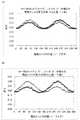
そこで、図2に示すように、有限要素法によるシミュレーションモデルとして、水晶片11の表裏に同一平面形状、同一サイズの第1及び第2励振用電極13a、13bを設けたモデルを設定した。さらに、第1及び第2の励振用電極13a、13b各々のエッジの位置、すなわち励振用電極の縁に沿った各所での振動変位を有限要素法により算出した。さらに、第1励振用電極13aに対し第2励振用電極13bの位置をずらした場合の上記振動変位をそれぞれ算出した。なお、励振用電極のエッジの各位置は、図2に示したように、角度γで特定されるエッジ上の位置、すなわち0°の位置、・・・180°の位置・・・とした。Therefore, as shown in FIG. 2, as a simulation model by the finite element method, a model in which the first and
図3、図4、図5は上記のシミュレーションにより求めた変位分布を示したものである。ただし、これらの図は、水晶片としてM−SCカット水晶片を用いかつCモードによる振動時のシミュレーション結果である。図3〜図5において、横軸は上記の角度γで特定される励振用電極のエッジの位置であり、縦軸はモデルの水晶片が振動した際の変位である。なお、変位は、最大変位により正規化した値で示してある。また、図3〜図5において、○でプロットした特性図は第1励振用電極13aのエッジの変位分布であり、+でプロットした特性図は第2励振用電極13bのエッジの変位分布である。ただし、発明者の種々のシミュレーションの取組結果から、M−SCカットの場合での角度βは、0.2°付近が良いことが判明しているので、図3〜図5に示した結果では、角度βを0.2°に固定した条件にて、角度αを35°、30°、25°、20°、15°0°と違えた場合の、第1及び第2の励振用電極のエッジの変位分布を示してある。
また、図6は、図3、図4、図5の結果の要点をまとめた図である。具体的には、角度αを違えた上記の6種類のシミュレーション各々について、第1励振電極のエッジでの変位分布と、第2励振電極のエッジでの変位分布との違いを、エッジの同位置での変位の差をエッジ全部に渡り積算した積算値で示したものである。従って、この積算値が小さいほど、表裏の励振電極のエッジでの変位分布の一致具合が高いことを示している。FIGS. 3, 4 and 5 show the displacement distribution obtained by the above simulation. However, these figures are the simulation results when the M-SC cut crystal piece is used as the crystal piece and the vibration is performed in the C mode. In FIGS. 3 to 5, the horizontal axis is the position of the edge of the excitation electrode specified by the above angle γ, and the vertical axis is the displacement when the crystal piece of the model vibrates. The displacement is shown as a value normalized by the maximum displacement. Further, in FIGS. 3 to 5, the characteristic diagram plotted with ◯ is the displacement distribution of the edge of the
Further, FIG. 6 is a diagram summarizing the main points of the results of FIGS. 3, 4, and 5. Specifically, for each of the above six types of simulations with different angles α, the difference between the displacement distribution at the edge of the first excitation electrode and the displacement distribution at the edge of the second excitation electrode is determined at the same position on the edge. The difference in displacement at is shown as an integrated value integrated over the entire edge. Therefore, the smaller the integrated value, the higher the degree of agreement of the displacement distributions at the edges of the front and back excitation electrodes.
図3〜図5を比較すること、及び、図6から明らかなように、第1励振用電極13aのエッジでの変位分布と、第2励振用電極のエッジでの変位分布とは、角度αを変えると変化することが分かる。そして、角度α=25°の場合(図4(A)参照)が、第1励振用電極13aのエッジでの変位分布と、第2励振用電極のエッジでの変位分布とが最も一致することが分かる。本シミュレーションを含む、発明者が実施した多くのシミュレーション結果から、M−SCカットの場合でかつCモードの場合では、角度α=25°付近かつ角度β=0.2°付近が、第1及び第2励振用電極のエッジでの変位分布は、最も一致することが分かった。然も、特に図6から明らかなように、振動子の特性改善効果を考慮すると、角度αは、−20〜−30°、すなわちα=25±5°が良く、さらに好ましくは、α=25±3°が良いことが分かる。また、βは、β=0±5°が良く、さらに好ましくは、β=0±3°が良いことが分かった。また、同様なシミュレーション結果から、M−SCカットの場合でかつBモードの場合では、角度α、角度βは、α=−6±5°、β=−17±5°が良く、さらに好ましくは、α=−6±3°、β=−6±3°が良いことが分かった。Comparing FIGS. 3 to 5, and as is clear from FIG. 6, the displacement distribution at the edge of the
他の水晶片として、SCカット、ITカット、ATカットについても上記と同様にシミュレーションを行い、これら水晶片での角度α、角度βの好ましい値を算出した。その結果を、上記のM−SCカットの結果と共に、下記表2に示した。As other crystal pieces, SC cut, IT cut, and AT cut were also simulated in the same manner as described above, and preferable values of the angles α and β of these crystal pieces were calculated. The results are shown in Table 2 below together with the results of the above M-SC cut.
2. 第2の実施形態
第1の実施形態では、表裏の励振用電極を上述の(1)〜(3)に示した所定の位置関係でずらすことにより、表裏の励振用電極のエッジでの変位分布を同じか又は近いものにできた。しかし、発明者のさらなる検討によれば、表裏の励振用電極を所定の位置関係でずらすとともに、励振電極の平面形状を楕円形状とし、かつ、水晶片のカット種別に応じて、楕円電極の楕円比率を所定範囲とし、かつ、楕円電極を水晶片に対し所定範囲で面内回転させて設けるのが良いことが判明した。こうすると、詳細は後述するが、励振用電極のエッジでの変位がエッジの各所で同じか近い値になり易いことが判明した。すなわち、励振用電極のエッジでの変位分布が平坦になり易いことが判明した。この第2実施形態はその例である。2. 2. Second Embodiment In the first embodiment, the displacement distribution at the edge of the front and back excitation electrodes is obtained by shifting the front and back excitation electrodes in the predetermined positional relationship shown in (1) to (3) above. Could be the same or similar. However, according to a further study by the inventor, the excitation electrodes on the front and back sides are shifted by a predetermined positional relationship, the planar shape of the excitation electrode is elliptical, and the ellipse of the elliptical electrode is determined according to the cut type of the crystal piece. It has been found that it is preferable to set the ratio within a predetermined range and to provide the elliptical electrode by in-plane rotation within a predetermined range with respect to the crystal piece. By doing so, although the details will be described later, it has been found that the displacement at the edge of the excitation electrode tends to be the same or close to each other at each part of the edge. That is, it was found that the displacement distribution at the edge of the excitation electrode tends to be flat. This second embodiment is an example.
図7(A)、(B)はその説明図である。この第2の実施形態の水晶振動子では、水晶片11に設ける第1励振用電極13a、第2励振用電極13b各々は、平面形状が楕円形状で所定の楕円比率のもので、かつ、水晶片に対し所定の角度範囲で面内回転していて、かつ、第1実施形態同様に所定関係(1)〜(3)でずらしたものとなっている。
ここで、楕円比率や面内回転角度は、以下のように定義する。楕円形状の励振電極の水晶片のX′軸に沿う寸法をa、Z′軸に沿う寸法をbとし(図7(A))、楕円比率をa/bと定義する。また、楕円形状の励振電極の水晶片に対する面内回転角度は、水晶片のX′軸に対する角度δと定義する(図7(B))。ただし、この角度δは、図7(B)に示したように、プラスY′面において、Y′軸を回転軸として、反時計方向への回転をプラス、時計方向への回転をマイナスと定義する。
このように定義した楕円比率a/b、面内回転角δを種々に変更したモデルを設定して、有限要素法を用いて第1及び第2励振用電極13a、13bのエッジでの変位分布を以下のように検討した。7 (A) and 7 (B) are explanatory views thereof. In the crystal oscillator of the second embodiment, each of the
Here, the ellipse ratio and the in-plane rotation angle are defined as follows. The dimension of the crystal piece of the elliptical excitation electrode along the X'axis is defined as a, the dimension along the Z'axis is defined as b (FIG. 7 (A)), and the elliptical ratio is defined as a / b. The in-plane rotation angle of the elliptical excitation electrode with respect to the crystal piece is defined as the angle δ of the crystal piece with respect to the X'axis (FIG. 7 (B)). However, as shown in FIG. 7B, this angle δ is defined as a plus Y'axis, a counterclockwise rotation as a plus, and a clockwise rotation as a minus, with the Y'axis as the rotation axis. To do.
Displacement distribution at the edges of the first and
2−1.楕円比率の検討
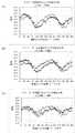
先ず、励振用電極の楕円比率の好ましい範囲を以下のように検討した。なお、シミュレーションは、水晶片をM−SCカットとし、振動モードをCモードの基本波モードとし、第1励振用電極13aと第2励振用電極13bとの位置関係を決めている角度α、βをα=25.5°、β=0.2°とし、励振用電極の水晶片に対する面内回転角δをδ=−9°とし、楕円比率を種々に変更して行った。なお、シミュレーションした楕円比率は、1.584、1.518、1.452、1.386、1.32、1.254、1.188、1.122、1.056であり、楕円比率1.32を基準に考えた場合、各楕円比率は、20%増、15%増、10%増、5%増、5%減、10%減、15%減、20%減のものに相当する。2-1. Examination of elliptical ratio First, the preferable range of the elliptic ratio of the excitation electrode was examined as follows. In the simulation, the crystal piece is M-SC cut, the vibration mode is the fundamental wave mode of C mode, and the angles α and β that determine the positional relationship between the
図8、図9、図10は上記の楕円比率のシミュレーションにより求めた、励振用電極のエッジでの変位分布を示したものである。図8〜図10において、横軸は第1の実施形態と同様に角度γで特定される励振用電極のエッジの位置であり、縦軸はモデルの水晶片が振動した際の変位である。なお、変位は、第1の実施形態と同様に、最大変位により正規化した値で示してある。また、図8〜図10において、○でプロットした特性図は第1励振用電極13aのエッジの変位分布であり、+でプロットした特性図は第2励振用電極13bのエッジの変位分布である。
また、図11は、図8、図9、図10の結果の要点をまとめた図である。具体的には、楕円比率を違えた上記の9種類のシミュレーション各々について、第1励振用電極のエッジでの変位分布と、第2励振用電極のエッジでの変位分布との違いを、表裏にかかわらず全部の変位の中の最大値と最小値との差で示したものである。この差が小さいほど、表裏の励振電極のエッジでの変位分布は平坦であることを示している。FIGS. 8, 9 and 10 show the displacement distribution at the edge of the excitation electrode obtained by the above simulation of the elliptic ratio. In FIGS. 8 to 10, the horizontal axis is the position of the edge of the excitation electrode specified by the angle γ as in the first embodiment, and the vertical axis is the displacement when the crystal piece of the model vibrates. The displacement is shown as a value normalized by the maximum displacement as in the first embodiment. Further, in FIGS. 8 to 10, the characteristic diagram plotted with ◯ is the displacement distribution of the edge of the
Further, FIG. 11 is a diagram summarizing the main points of the results of FIGS. 8, 9, and 10. Specifically, for each of the above nine types of simulations with different elliptic ratios, the difference between the displacement distribution at the edge of the first excitation electrode and the displacement distribution at the edge of the second excitation electrode is shown on the front and back. Regardless, it is shown by the difference between the maximum and minimum values of all displacements. The smaller this difference is, the flatter the displacement distribution at the edges of the front and back excitation electrodes is.
図8〜図10から先ず明らかなことは、表裏の励振用電極を所定の位置関係でずらした第1の実施形態の効果により、第1励振用電極13a及び第2励振用電極13b各々のエッジでの変位分布は、楕円比率を変えても、同じような傾向、すなわち両者は略正弦波状の変位分布を示している。ところが、図8〜図10を比較することと、特に図11から明らかなように、第1及び第2励振用電極13a、13bのエッジでの変位分布各々の平坦性は、楕円比率を変えることで変化することが分かる。すなわち、変位分布は、楕円比率が1.32のとき最も平坦になり(図9(B)参照)、楕円比率が1.32に対し増減すると徐々に正弦波状となり凹凸し始めることが分かる。励振用電極のエッジでの変位分布が平坦である方が、そうでない場合に比べ、不要振動の抑制等に好ましいと考えられるので、所定の楕円比率を有する励振用電極は有用と言える。The first thing that is clear from FIGS. 8 to 10 is the edge of each of the
楕円比率1.32を基準にした場合のシミュレーション結果によれば、M−SCカットで、Cモードで振動し、基本波で振動する、水晶振動子の場合では、楕円比率は、1.32±10%の範囲が良く、より好ましくは1.32±5%の範囲が良い。このシミュレーション手順に従いM−SCカットの3倍波、5倍波、Bモードでの基本波、3倍波、5倍波についての好ましい楕円比率も検討した。これら検討により決定した、各水準での好ましい楕円比率を、下記表3の楕円比率の欄に示した。また、同様にして、SCカット、ITカット、ATカット各々での好ましい楕円比率を決定した。これら結果を、下記表4、表5、表6各々の楕円比率の欄に示した。また、発明者のシミュレーション結果の検討によれば、各カット種別での励振用電極の楕円比率の好ましい許容範囲は、±10%、より好ましくは±5%と判断できた。According to the simulation results when the ellipse ratio is 1.32, the ellipse ratio is 1.32 ± in the case of a crystal oscillator that vibrates in C mode and vibrates in the fundamental wave with M-SC cut. The range of 10% is good, more preferably the range of 1.32 ± 5%. According to this simulation procedure, preferable elliptic ratios for M-SC cut 3rd harmonic, 5th harmonic, fundamental wave in B mode, 3rd harmonic, and 5th harmonic were also examined. The preferred ellipse ratio at each level determined by these studies is shown in the column of ellipse ratio in Table 3 below. Further, in the same manner, a preferable ellipse ratio for each of the SC cut, the IT cut, and the AT cut was determined. These results are shown in the columns of elliptical ratios in Tables 4, 5, and 6 below. Further, according to the examination of the simulation results of the inventor, it was determined that the preferable allowable range of the elliptical ratio of the excitation electrodes for each cut type was ± 10%, more preferably ± 5%.
2−2.励振用電極の水晶片に対する面内回転角度の検討
次に、楕円形状の励振用電極の水晶片に対する面内回転角度δの適正範囲について説明する。
先ず、水晶片をM−SCカットとし、振動モードをCモードの基本波モードとし、第1励振用電極13aと第2励振用電極13bとの位置関係を決めている角度α、βをα=25.5°、β=0.2°とし、楕円比率を1.32とした条件で、シミュレーションした結果は下記の通りであった。なお、シミュレーションの際の角度δは、1°、−1.5°、−4°、−6.5°、−9°、−11.5°、−14°、−16.5°、−19°である。ここで、角度δの向きは、図7(B)に示した通り、Y′軸を回転軸として、水晶片11のプラスY′面において反時計回りをプラス、時計周りをマイナスと定義している。2-2. Examination of the in-plane rotation angle of the excitation electrode with respect to the crystal piece Next, the appropriate range of the in-plane rotation angle δ of the elliptical excitation electrode with respect to the crystal piece will be described.
First, the crystal piece is set to M-SC cut, the vibration mode is set to the fundamental wave mode of C mode, and the angles α and β that determine the positional relationship between the
図12、図13、図14は、上記のシミュレーションにより求めた変位分布を示したものである。図12〜図14において、横軸は第1の実施形態と同様に角度γで特定される励振用電極のエッジの位置であり、縦軸はモデルの水晶片が振動した際の変位である。なお、変位は、第1の実施形態と同様に、最大変位により正規化した値で示してある。また、図10〜図12において、○でプロットした特性図は第1励振用電極13aのエッジの変位分布であり、+でプロットした特性図は第2励振用電極13bのエッジの変位分布である。
また、図15は、図12、図13、図14の結果の要点をまとめた図である。具体的には、面内回転角度δを違えた上記の9種類のシミュレーション各々について、第1励振用電極のエッジでの変位分布と、第2励振用電極のエッジでの変位分布との違いを、表裏にかかわらず全部の変位の中の最大値と最小値との差で示したものである。この差が小さいほど、表裏の励振電極のエッジでの変位分布は平坦であることを示している。12, 13 and 14 show the displacement distribution obtained by the above simulation. In FIGS. 12 to 14, the horizontal axis is the position of the edge of the excitation electrode specified by the angle γ as in the first embodiment, and the vertical axis is the displacement when the crystal piece of the model vibrates. The displacement is shown as a value normalized by the maximum displacement as in the first embodiment. Further, in FIGS. 10 to 12, the characteristic diagram plotted with ◯ is the displacement distribution of the edge of the
Further, FIG. 15 is a diagram summarizing the main points of the results of FIGS. 12, 13, and 14. Specifically, for each of the above nine types of simulations with different in-plane rotation angles δ, the difference between the displacement distribution at the edge of the first excitation electrode and the displacement distribution at the edge of the second excitation electrode , It is shown by the difference between the maximum value and the minimum value in all displacements regardless of the front and back. The smaller this difference is, the flatter the displacement distribution at the edges of the front and back excitation electrodes is.
図12〜図14を比較することで明らかなように、また、図15から明らかなように、第1及び第2励振用電極13a、13bのエッジでの変位分布は、楕円の方向である角度δを変えることで変化することが分かる。すなわち、M−SCカットの場合は、第1及び第2励振用電極各々のエッジでの変位分布は、δ=−9°のとき他のものと比べて最も平坦、かつ、両者が同じようになり、角度δが−9°から増減すると凹凸が増えて行きかつ両者の違いも大きくなることが分かる。従って、角度δは−9°が良く、また、発明者のシミュレーション結果によればその許容範囲は±5°、より好ましくは±3°が良いと判断できた。このシミュレーション手順に従い、M−SCカットのCモードでの3倍波、5倍波、M−SCカットのBモードでの基本波、3倍波、5倍波、さらに、SCカット、ITカット、ATカット各々での、各モード及び基本波、3倍波、5倍波各々での好ましい角度δを決定した。これら結果を、上記の表3、表4、表5、表6各々の楕円の方向の欄に示した。なお、いずれの場合も、楕円の方向δの好ましい許容範囲は±5°、より好ましくは±3°と判断できた。As is clear from the comparison of FIGS. 12 to 14, and as is clear from FIG. 15, the displacement distribution at the edges of the first and
3. 実際の構造例
上記した実施形態の水晶振動子の実際の構造例について説明する。図16(A),(B)はその説明図である。
図16(A)に示した構造例は、リード型の水晶振動子20に本発明を適用した例であり、水晶振動子20を側面から見た概略図である。この水晶振動子20は、ベース21と、このベースに設けたリード23と、リードの先端に設けたクリップ端子25とを具える。そして、クリップ端子25に水晶片11を固定した構造となっている。詳細には、水晶片11の表裏には励振用電極13a、13bから引き出されている引出電極15を設けてあり、水晶片11は引出電極15の末端付近でクリップ端子25に導電性接着剤27で固定してある。そして、実際は、水晶片11を密閉するため図示しないキャップがベースに接合されている。
図16(B)に示した構造例は、表面実装型の水晶振動子30に本発明を適用した例であり、水晶振動子30を上面から見た概略図である。この水晶振動子30は、セラミックベース31と、このベースに設けた支持パッド33とを具える。そして、支持パッド33に水晶片11を固定した構造となっている。詳細には、水晶片11の表裏には励振用電極13a、13bから引き出されている引出電極15を設けてあり、水晶片11は引出電極15の末端付近で支持パッド33に導電性接着剤35で固定してある。そして、実際は、水晶片11を密閉するため図示しない蓋部材がベースに接合されている。また、セラミックベース外側底面に、実装端子(図示せず)を具えていて、この実装端子は支持パッドに電気的に接続してある。
もちろん、これら構造例はこの発明の好適例であり、他の構造であっても良い。3. 3. Actual Structural Example An actual structural example of the crystal unit of the above-described embodiment will be described. 16 (A) and 16 (B) are explanatory views thereof.
The structural example shown in FIG. 16A is an example in which the present invention is applied to the lead-
The structural example shown in FIG. 16B is an example in which the present invention is applied to the surface mount
Of course, these structural examples are preferable examples of the present invention, and other structures may be used.
4. 第3の実施形態(励振用電極の縁部に傾斜部を設ける形態)
上述した第1、第2の実施形態では、励振用電極は、その厚さが全域にわたって実質的に同じ構成であった。しかし、励振用電極の縁部に傾斜部を設けると、不要モードの抑制に対しさらに好ましい。この第3の実施形態はその例である。
図17は、この第3の実施形態の水晶振動子の説明図である。特に、第3の実施形態の水晶振動子に具わる水晶片41に着目した図であり、(A)図は水晶片41の平面図、(B)図は水晶片40のR−R線に沿った部分的断面図である。なお、図17(B)では、励振用電極13a,13bの傾斜部13ab、13bbの理解を深めるために励振用電極の厚みを実際より拡大して示してある。4. Third embodiment (a form in which an inclined portion is provided at the edge of the excitation electrode)
In the first and second embodiments described above, the excitation electrodes have substantially the same thickness over the entire area. However, it is more preferable to provide an inclined portion at the edge of the excitation electrode for suppressing unnecessary modes. This third embodiment is an example.
FIG. 17 is an explanatory diagram of the crystal unit of the third embodiment. In particular, it is a figure focusing on the
この水晶片41は、その表裏に設ける励振用電極13a、13b各々が、一定の厚さで形成される主厚部13aa、13baと、これら主厚部の周囲に形成され主厚部に接する部分から励振用電極の最外周にかけて厚さが徐々に薄くなるように形成された傾斜部13ab、13bbを具えたことが特徴である。なお、主厚部13aa、13baの厚さが一定とは、製造上の不可避的な変動によるバラツキは許容するものである。
傾斜部13abは、この例の場合は、4段の段差で構成してある。そして、主厚部13aa側から励振用電極13aの最外周までの幅すなわち傾斜幅がXAに形成されており、各段差間の幅がXBに形成されている。すなわち、この例の場合は、幅XAは幅XBの3倍の長さに形成されている。主厚部13aaの厚さはYAに形成されている。また、傾斜部13abの各段差の高さはYBに形成されている。そのため、厚さYAは高さYBの4倍の厚さとなっている。The
In the case of this example, the inclined portion 13ab is composed of four steps. The width from the main thick portion 13aa side to the outermost circumference of the
これら傾斜部13ab、13bbの効果について、以下の通りのシミュレーションを行い確認した。すなわち、水晶片41のシミュレーションモデルとして、ATカット水晶片を用いたモデルと、M−SCカット水晶片を用いたモデルの2種のモデルを用意した。そして、これらモデルの励振用電極の主厚部13aa、13ba各々の膜厚YAを140nm、主振動の周波数を26MHzとし、傾斜部13ab、13bbの幅XAを種々に変化させた場合での、有限要素法によるシミュレーションを行った。
水晶振動子では、主振動(例えばCモード)と共に主振動とは異なり設計上意図されない振動である不要振動が生じる。ATカット、M−SCカット等の水晶材料により形成され厚みすべり振動で振動する水晶振動子では、不要振動として特に屈曲振動によるものの影響が大きい。図18のグラフの横軸には、この屈曲振動の波長である屈曲波長λで規格化された傾斜幅を示してある。そのため、図18のグラフに示した傾斜幅は、同一の目盛でも水晶片がATカットかM−SCカットかで傾斜部13ab、13bbの傾斜幅の寸法が異なる。例えば、26MHzの振動周波数による振動を主振動とした場合では、ATカット水晶片での屈曲波長λは約100μmとなり、M−SCカット水晶片での屈曲波長λは約110μmとなる。このとき図18のグラフにおいて「1」で示される傾斜幅の実際の寸法は1×λであり、ATカット水晶片の場合は傾斜幅が1×λ=約100μmとなり、M−SCカット水晶片の場合は傾斜幅が1×λ=約110μmとなる。The effects of these inclined portions 13ab and 13bb were confirmed by performing the following simulations. That is, as a simulation model of the
In the crystal unit, the main vibration (for example, C mode) and the unnecessary vibration, which is an unintended vibration by design, are generated unlike the main vibration. In a crystal oscillator formed of a crystal material such as AT cut or M-SC cut and vibrating by thickness sliding vibration, the influence of bending vibration is particularly large as unnecessary vibration. The horizontal axis of the graph of FIG. 18 shows the inclination width standardized by the bending wavelength λ, which is the wavelength of the bending vibration. Therefore, in the inclination width shown in the graph of FIG. 18, the dimensions of the inclination widths of the inclined portions 13ab and 13bb differ depending on whether the crystal piece is AT cut or M-SC cut even if the scale is the same. For example, when vibration with a vibration frequency of 26 MHz is used as the main vibration, the bending wavelength λ of the AT-cut quartz piece is about 100 μm, and the bending wavelength λ of the M-SC-cut quartz piece is about 110 μm. At this time, the actual dimension of the inclination width indicated by "1" in the graph of FIG. 18 is 1 × λ, and in the case of the AT-cut crystal piece, the inclination width is 1 × λ = about 100 μm, and the M-SC-cut crystal piece. In the case of, the inclination width is 1 × λ = about 110 μm.
図18のグラフの縦軸には、主振動の振動エネルギーの損失を示すQ値の逆数を示してある。また、ATカット水晶片のモデルの特性は黒丸●で示し、M−SCカット水晶片のモデルでの特性は黒三角▲で示してある。
図18から分かるように、両モデルともに、屈曲波長λで規格化された傾斜幅が約「0.5」から「3」となる範囲で振動エネルギーの損失を示す1/Qが3.0×10−6(図18では「3.0E−6」と表記)以下と低くなっている。すなわち、傾斜幅が屈曲波長λの0.5倍以上3倍以下の長さに形成される場合に振動エネルギーの損失が抑えられていることが分かる。特に、両モデルともに、屈曲波長λで規格化された傾斜幅が「1」から「2.5」の範囲において1/Qの大きさが低く、さらにその変動も少なくなっている。すなわち、傾斜幅が屈曲波長の1倍から2.5倍の長さである場合には、さらに安定して振動エネルギーの損失が低くなることが分かる。The vertical axis of the graph of FIG. 18 shows the reciprocal of the Q value indicating the loss of vibration energy of the main vibration. The characteristics of the AT-cut crystal piece model are indicated by black circles ●, and the characteristics of the M-SC-cut crystal piece model are indicated by black triangles ▲.
As can be seen from FIG. 18, in both models, 1 / Q indicating the loss of vibration energy in the range where the inclination width standardized by the bending wavelength λ is about “0.5” to “3” is 3.0 ×. It is as low as 10-6 (denoted as "3.0E-6" in FIG. 18) or less. That is, it can be seen that the loss of vibration energy is suppressed when the inclination width is formed to have a length of 0.5 times or more and 3 times or less of the bending wavelength λ. In particular, in both models, the magnitude of 1 / Q is low in the range of the inclination width standardized by the bending wavelength λ from “1” to “2.5”, and the fluctuation is also small. That is, it can be seen that when the inclination width is 1 to 2.5 times the bending wavelength, the loss of vibration energy is more stable and lower.
励振用電極の縁部に傾斜部を設ける構成は、特に、水晶片が平板上のものに適用して好適である。水晶振動子の特性向上を図るため、水晶片自体の縁領域の厚さが薄いいわゆるコンベックス形状の水晶片が従来から用いられている。こうすることで、振動エネルギーを閉じ込め、不要振動を抑圧することができる。しかし、水晶片をコンベックス形状にするためには加工の手間とコストがかかるという問題がある。この第3実施形態の場合は、励振用電極の縁部の傾斜部が水晶片のコンベックス形状の役割を示す。従って、表裏の励振用電極を所定関係でずらすという第1及び第2の実施形態で例示した本発明の構成に対し、上記の傾斜部の構造をさらに加えた場合、水晶振動子の特性向上やコスト低減がさらに図れる。 The configuration in which the inclined portion is provided at the edge of the excitation electrode is particularly suitable for applications where the crystal piece is on a flat plate. In order to improve the characteristics of the crystal unit, a so-called convex-shaped crystal piece having a thin edge region of the crystal piece itself has been conventionally used. By doing so, it is possible to confine the vibration energy and suppress unnecessary vibration. However, there is a problem that it takes time and cost to process the crystal piece into a convex shape. In the case of this third embodiment, the inclined portion of the edge portion of the excitation electrode shows the role of the convex shape of the crystal piece. Therefore, when the structure of the inclined portion is further added to the configuration of the present invention illustrated in the first and second embodiments in which the excitation electrodes on the front and back sides are shifted in a predetermined relationship, the characteristics of the crystal oscillator are improved. Cost can be further reduced.
5. 第4の実施形態(片面の励振用電極の縁部に傾斜部を設ける形態)
上述した第3の実施形態では、表裏の励振用電極各々の縁部に傾斜部を設ける構造を説明した。しかし、水晶振動子を製造する場合、振動周波数を調整するためにアルゴンのイオンビーム等により励振用電極をトリミングすることが行われる。このトリミング工程において、傾斜部が消失し、これによって振動エネルギーの損失が大きくなる場合がある。これを回避するため、水晶片の周波数調整面の励振用電極には傾斜部は設けず、周波数調整面とは反対面の励振用電極のみに傾斜部を設けても良い。この第4の実施形態はその例である。5. Fourth embodiment (a form in which an inclined portion is provided at the edge of the excitation electrode on one side)
In the third embodiment described above, a structure in which an inclined portion is provided on the edge portion of each of the front and back excitation electrodes has been described. However, in the case of manufacturing a crystal oscillator, the excitation electrode is trimmed with an argon ion beam or the like in order to adjust the vibration frequency. In this trimming step, the inclined portion disappears, which may increase the loss of vibration energy. In order to avoid this, the excitation electrode on the frequency adjusting surface of the crystal piece may not be provided with an inclined portion, and the inclined portion may be provided only on the excitation electrode on the surface opposite to the frequency adjusting surface. This fourth embodiment is an example.
図19は、この第4の実施形態の水晶振動子の説明図である。特に、第4の実施形態の水晶振動子に具わる水晶片51に着目した図であり、(A)図は水晶片51の平面図、(B)図は水晶片51のS−S線に沿った部分的断面図である。この第4の実施形態の場合、水晶片の周波数調整がされない側の励振用電極のみがその縁部に傾斜部を有した構造となっている。図19の例では、励振用電極13a、13bのうちの励振用電極13bのみが、主厚部13baと傾斜部13bbとを有した構造となっている。この励振用電極13bの構成は、第3の実施形態で説明した構成で良い。すなわち、第3の実施形態で説明したように、励振用電極13bは、一定の厚さYA2(第3の実施形態でのYA)で形成される主厚部13baと、この主厚部13bの周囲に形成され主厚部に接する部分から励振用電極の最外周にかけて厚さが徐々に薄くなるように形成された傾斜部13bbを具えるとともに、傾斜幅XAが屈曲波長λの0.5倍以上3倍以下、好ましくは1倍から2.5倍の長さとしてある。一方、傾斜部を設けない側の励振用電極13aの膜厚はYA1としてある。なお、膜厚YA1、YA2の構成の詳細は後述する。この水晶片51を、励振用電極13b側が周波数調整されない側となるように、水晶振動子用の容器(例えば図16参照)に実装する。FIG. 19 is an explanatory diagram of the crystal unit of the fourth embodiment. In particular, it is a figure focusing on the
次に、この第4の実施形態を実施するに当たり留意すべき事項について図20を参照しながら以下に説明する。
図20は、シミュレーションモデルとして、以下の3種類のシミュレーションモデルを用意し、各モデルでの主振動エネルギーの損失(1/Q)を有限要素法により解析した結果を示したものである。3種類のうちの1つ目は第4の実施形態の水晶片51に当たるモデル、すなわち水晶片の片面の励振用電極のみに傾斜部を設けたモデルである。2つ目は第3の実施形態の水晶片41に当たるモデル、すなわち水晶片の両面の励振用電極に傾斜部を設けたモデルである。3つ目は第1の実施形態の水晶片11に当たるモデル、すなわち水晶片の励振用電極に傾斜部を設けないモデルである。Next, matters to be noted in carrying out this fourth embodiment will be described below with reference to FIG.
FIG. 20 shows the results of preparing the following three types of simulation models as simulation models and analyzing the loss (1 / Q) of the main vibration energy in each model by the finite element method. The first of the three types is a model corresponding to the
いずれのモデルも水晶材料をM−SCカットとし、励振用電極の全てを金(Au)とし、主振動の周波数を30MHz(屈曲波長λが約95μm)とし、傾斜部を設けたモデルでの傾斜幅XAを133μm(屈曲波長λの1.4倍)としている。なお、励振用電極の膜厚であるが、図20のグラフでは、横軸に励振用電極13aの厚さYA1と、励振用電極13bの主厚部13baの厚さYA2を示してある。そして、このシミュレーションの場合は、厚さYA1と厚さYA2との合計が常に280nmとしてあり、図20では厚さYA2がグラフの右側に向かうに従って増加している。また、図20の縦軸には主振動(例えばCモード)の振動エネルギーの損失(1/Q)を示してある。そして、図20では、片面の励振用電極のみに傾斜部を設けたモデルの計算結果を黒丸●で示し、両面の励振用電極に傾斜部を設けたモデルの計算結果を黒菱形◆で示し、励振用電極に傾斜部を設けないモデルの計算結果を白四角□で示してある。
なお、厚さYA1と厚さYA2との合計が常に280nmとなる条件でシミュレーションする理由は、水晶振動子において、いわゆるエネルギー閉じ込めを確保するためである。すなわち、エネルギー閉じ込めを確保した前提で、本発明の効果を確認したいためである。ただし、280nmという値は、実施形態の水晶片の大きさ、形状、周波数に応じた一つの例である。In both models, the crystal material is M-SC cut, all the excitation electrodes are gold (Au), the frequency of the main vibration is 30 MHz (bending wavelength λ is about 95 μm), and the tilted part is provided. The width XA is 133 μm (1.4 times the bending wavelength λ). Regarding the film thickness of the excitation electrode, in the graph of FIG. 20, the thickness YA1 of the
The reason for simulating under the condition that the total of the thickness YA1 and the thickness YA2 is always 280 nm is to secure so-called energy confinement in the crystal oscillator. That is, it is necessary to confirm the effect of the present invention on the premise that energy confinement is secured. However, the value of 280 nm is an example according to the size, shape, and frequency of the crystal piece of the embodiment.
図20から分かるように、片面の励振用電極のみに傾斜部を設けたモデルでは、厚さYA1及び厚さYA2が140nmである場合に、振動エネルギーの損失を示す1/Qが約5.5×10−6(図20のグラフでは「×10−6」を「E−6」と表記)となっている。しかし、このモデルでは、傾斜部が形成されていない励振用電極の厚さYA1を薄くし、その代わりに傾斜部を設けた励振用電極の厚さYA2を厚くすることで1/Qが低下し、厚さYA1が60nm、厚さYA2が220nmとなる場合に1/Qが約3.1×10−6となる。すなわち、片面の励振用電極のみに傾斜部を設けたモデルでは、片面の励振用電極のみに傾斜部を設けるとともに、傾斜部を設けない励振用電極の厚さを薄くすることで、水晶振動子の損失が低下することが分かる。一方、両面の励振用電極に傾斜部を持っているモデルでは、厚さYA1と厚さYA2を変更した場合でも、1/Qは約2.4×10−6〜約2.6×10−6と、横ばい状態であり、一見すると特性としては好ましい。しかし、両面の励振用電極に傾斜部を持っているモデルでは、周波数調整時に周波数調整面側の励振用電極の傾斜部が消失することが起きるので、実製品ではこの特性は維持できない。また、両面の励振用電極に傾斜部を持っていないモデルでは、厚さYA1と厚さYA2を変更した場合、厚さYA2が増えるに従って1/Qが大きくなり、厚さYA2が220nmのときに1/Qが約9.9×10−6となっている。すなわち、両面の励振用電極に傾斜部を持っていないモデルでは、YA2の厚さが厚くなるに従いこの励振電極の縁部での段差に起因した不要モードが生じて、損失が増加する。As can be seen from FIG. 20, in the model in which the inclined portion is provided only on the excitation electrode on one side, 1 / Q indicating the loss of vibration energy is about 5.5 when the thickness YA1 and the thickness YA2 are 140 nm. It is × 10-6 (in the graph of FIG. 20, “× 10-6” is expressed as “E-6”). However, in this model, 1 / Q is reduced by reducing the thickness YA1 of the excitation electrode on which the inclined portion is not formed and increasing the thickness YA2 of the exciting electrode provided with the inclined portion instead. When the thickness YA1 is 60 nm and the thickness YA2 is 220 nm, 1 / Q is about 3.1 × 10⁻⁶. That is, in the model in which the inclined portion is provided only on the excitation electrode on one side, the crystal oscillator is provided by providing the inclined portion only on the excitation electrode on one side and reducing the thickness of the excitation electrode without the inclined portion. It can be seen that the loss of On the other hand, in the model having inclined portions on the excitation electrodes on both sides, 1 / Q is about 2.4 × 10⁻⁶ to about 2.6 × 10- even when the thickness YA1 and the thickness YA2 are changed. 6 is in a flat state, and at first glance, it is preferable as a characteristic. However, in a model having an inclined portion on both sides of the excitation electrode, the inclined portion of the excitation electrode on the frequency adjusting surface side may disappear at the time of frequency adjustment, so that this characteristic cannot be maintained in the actual product. Further, in the model in which the excitation electrodes on both sides do not have an inclined portion, when the thickness YA1 and the thickness YA2 are changed, 1 / Q increases as the thickness YA2 increases, and when the thickness YA2 is 220 nm. 1 / Q is about 9.9 × 10⁻⁶. That is, in the model in which the excitation electrodes on both sides do not have an inclined portion, as the thickness of the YA2 increases, an unnecessary mode due to a step at the edge portion of the excitation electrode occurs, and the loss increases.
この第4の実施形態の水晶振動子での効果は以下の理由で生じる。水晶振動子では、主振動(例えばCモード)と共に主振動とは異なり設計上意図されない振動である不要振動が生じる。ATカット及びM−SCカット等の水晶材料により形成され厚みすべり振動で振動する水晶片により形成される水晶振動子では、主振動以外の他のモードが主振動の発振を阻害する不要モードとなる。不要モードによる振動である不要振動では、屈曲振動が特に主振動に影響を及ぼすものとして知られている。屈曲振動は、主に励振電極の端部で振動エネルギーが屈曲振動に変換されることによりそれが主振動に重畳し、屈曲振動が圧電振動片全体で振動するため、水晶片が保持される導電性接着剤に振動エネルギーが吸収される。このような屈曲振動によるエネルギーの損失は振動エネルギーの損失につながる。
この第4の実施形態の水晶振動子であって、励振用電極の膜厚YA1、YA2がともに140nmの場合は、励振用電極13bに傾斜部13bbが形成されているものの、励振用電極13aには傾斜部が形成されていないので、屈曲振動の主振動に対する影響が十分に抑えられていないため、損失は傾斜部を設けないモデルと同等となり大きい。しかし、第4の実施形態に係る水晶振動子では、傾斜部を設けていない励振用電極13aの厚さYA1が薄くなるに従って1/Qが低下し、厚さYA1が60nmである場合に損失は、両面の励振用電極に傾斜部を設けたモデルに近くなる。これは傾斜部を設けていない励振用電極の厚さYA1が薄くなることにより、電極端部の段差の影響が軽減されるので、屈曲振動の発生が抑えられるためと考えられる。従って、第4の実施形態の場合は、傾斜部を設けていない励振用電極13bの厚さYA1は、励振用電極13bの端部で不要モードの誘発を抑制できかつ電極本来の導電膜としての機能が得られることを前提に極力薄い方が好ましい。薄膜技術において膜として成立し得る下限の範囲が60nmから100nmの厚さであることが知られており、これを考慮すると傾斜部を設けていない励振用電極の機能を発揮させるためには、厚さYA1は、60nm〜100nm、好ましくは60nmから80nmの範囲にあることが好ましい。The effect of the crystal unit of the fourth embodiment occurs for the following reasons. In the crystal unit, the main vibration (for example, C mode) and the unnecessary vibration, which is an unintended vibration by design, are generated unlike the main vibration. In a crystal oscillator formed of a crystal piece formed of a crystal material such as AT cut and M-SC cut and vibrating by thickness sliding vibration, modes other than the main vibration are unnecessary modes that hinder the oscillation of the main vibration. .. In the unnecessary vibration, which is the vibration due to the unnecessary mode, it is known that the bending vibration particularly affects the main vibration. In bending vibration, vibration energy is converted into bending vibration mainly at the end of the excitation electrode, which is superimposed on the main vibration, and the bending vibration vibrates in the entire piezoelectric vibration piece, so that the crystal piece is held. Vibration energy is absorbed by the sex adhesive. The energy loss due to such bending vibration leads to the loss of vibration energy.
In the crystal oscillator of the fourth embodiment, when the thicknesses YA1 and YA2 of the excitation electrodes are both 140 nm, the
また、第4の実施の形態の水晶片51では水晶片51がベベル加工又はコンベックス加工などの加工がされない代わりに励振電極を所定の厚さに形成することにより振動エネルギーを閉じ込めている。励振用電極の厚さYA1とYA2との合計厚さが振動エネルギ−閉じ込めを行える膜厚となるように、傾斜部を設けていない励振用電極の厚さYA2を選択するのが良い。具体的には、両励振用電極の厚さの合計が水晶片の板厚に対して数%程度の値から、圧電振動片の大きさや周波数等を考慮して決めることができ、例えば2〜5%から選ぶのが良い。
この第4の実地形態の場合は、表裏の励振用電極を所定関係でずらすという第1、第2の実施形態で例示した本発明の効果が得られるとともに、励振用電極に傾斜部を設ける効果と、この傾斜部が周波数調整時に損傷することを回避できるという効果が得られる。Further, in the
In the case of this fourth practical embodiment, the effect of the present invention illustrated in the first and second embodiments of shifting the front and back excitation electrodes in a predetermined relationship can be obtained, and the effect of providing an inclined portion on the excitation electrode is obtained. Then, the effect that this inclined portion can be prevented from being damaged at the time of frequency adjustment can be obtained.
6. 第5の実施形態(高調波も考慮した傾斜部の形態)
上述した第3の実施形態、第4の実施形態では、傾斜部の長さである傾斜幅XAについて、基本波に関する適正値を説明した。一方、水晶振動子の用途の1つとして、1つの水晶振動子から2つの周波数の信号を同時出力する用途がある。例えば、国際公開第2015/133472号には、基本波と高調波とを1つの水晶片から取り出すことが記載されている。このようなものでは、一方の周波数を出力信号とし、他方の周波数を温度補償のセンサ用信号として使用することができ、然も、2つの周波数を1つの水晶振動子で得られるので、水晶片の個体差の影響を軽減できる等、好ましい。この第5の実施形態は、上述した第1〜第4の実施形態において、さらに、基本波と高調波とを考慮した設計に関するものである。
この第5の実施形態の水晶片は、第1の実施形態〜第4の実施形態の種々の形態において、励振用電極に傾斜部を設ける場合の傾斜幅を、厚みすべり振動の基本波での屈曲振動の波長である第1屈曲波長の0.84倍以上1.37倍以下であり、厚みすべり振動の3倍波での屈曲振動の波長である第2屈曲波長の2.29倍以上3.71倍以下の長さとすることを特徴とする。6. Fifth embodiment (form of inclined portion in consideration of harmonics)
In the third embodiment and the fourth embodiment described above, the appropriate value regarding the fundamental wave has been described for the inclination width XA which is the length of the inclined portion. On the other hand, one of the uses of the crystal oscillator is to simultaneously output signals of two frequencies from one crystal oscillator. For example, International Publication No. 2015/133472 describes the extraction of fundamentals and harmonics from a single crystal piece. In such a case, one frequency can be used as an output signal and the other frequency can be used as a sensor signal for temperature compensation, and since two frequencies can be obtained by one crystal oscillator, a crystal piece It is preferable that the influence of individual differences can be reduced. The fifth embodiment relates to the design in consideration of the fundamental wave and the harmonics in the first to fourth embodiments described above.
In the various embodiments of the first to fourth embodiments, the crystal piece of the fifth embodiment has an inclination width when an inclined portion is provided on the excitation electrode, and the inclination width is set to the fundamental wave of the thickness sliding vibration. It is 0.84 times or more and 1.37 times or less of the first bending wavelength which is the wavelength of bending vibration, and 2.29 times or more and 2.29 times or more of the second bending wavelength which is the wavelength of bending vibration in the third harmonic of thickness slip vibration. It is characterized by having a length of .71 times or less.
図21はこの第5の実施形態の効果を説明するためのシミュレーション結果を示した図である。具体的には、図21は、図17を用いて説明した両面の励振用電極に傾斜部を設けたシミュレーションモデルについて、励振用電極の傾斜幅を屈曲振動の波長で正規化した値と、振動エネルギーの損失(1/Q)との関係を示したグラフである。シミュレーションモデルは、励振用電極の全てが金(Au)で形成され、Cモードを主振動とした場合の基本波(周波数:30MHz)及び3倍波(周波数:90MHz)について、主厚部13aa(13ba)の膜厚YA1が100nm、140nm、180nmの場合のシミュレーションによる計算結果が示されている。FIG. 21 is a diagram showing simulation results for explaining the effect of the fifth embodiment. Specifically, FIG. 21 shows the value obtained by normalizing the inclination width of the excitation electrode with the wavelength of bending vibration and the vibration of the simulation model in which the excitation electrodes on both sides provided with the inclination portions described with reference to FIG. It is a graph which showed the relationship with the energy loss (1 / Q). In the simulation model, the main thickness portion 13aa (frequency: 90 MHz) for the fundamental wave (frequency: 30 MHz) and the triple wave (frequency: 90 MHz) when all the excitation electrodes are made of gold (Au) and the C mode is the main vibration. The calculation results by the simulation when the film thickness YA1 of 13ba) is 100 nm, 140 nm, and 180 nm are shown.
図21のグラフの横軸は、傾斜幅XA(μm)が示されている。図21のグラフの縦軸では、主振動の振動エネルギーの損失を示すQ値の逆数が示されている。また図21では、主厚部の厚さYAが100nmで基本波を発振した場合の水晶片の損失を白抜きの四角□で示し、厚さYAが140nmで基本波を発振した場合の水晶片の損失を白抜きの三角△で示し、厚さYAが180nmで基本波を発振した場合の水晶片の損失を白抜きの丸○で示し、主厚部の厚さYAが100nmで3倍波を発振した場合の水晶片の損失を黒四角■で示し、厚さYAが140nmで3倍波を発振した場合の水晶片の損失を黒三角▲で示し、厚さYAが180nmで3倍波を発振した場合の水晶片の損失を黒丸●で示してある。 The horizontal axis of the graph of FIG. 21 shows the inclination width XA (μm). The vertical axis of the graph of FIG. 21 shows the reciprocal of the Q value indicating the loss of vibration energy of the main vibration. Further, in FIG. 21, the loss of the crystal piece when the fundamental wave is oscillated at a thickness YA of the main thickness portion of 100 nm is shown by a white square □, and the crystal piece when the fundamental wave is oscillated at a thickness YA of 140 nm. The loss of the crystal piece is indicated by a white triangle Δ, and the loss of the crystal piece when the fundamental wave is oscillated at a thickness YA of 180 nm is indicated by a white circle ○. The loss of the crystal piece when oscillating is indicated by a black square ■, the loss of the crystal piece when oscillating a triple wave with a thickness YA of 140 nm is indicated by a black triangle ▲, and the loss of the crystal piece when the thickness YA is 180 nm is a triple wave. The loss of the crystal piece when oscillating is indicated by a black circle.
図21から分かるように、3倍波における傾斜幅と振動エネルギーの損失(1/Q)との関係が、主厚部の厚さYAの大きさに関わらず似たような傾向を示しており、傾斜幅XAが約30μmから約130μmの範囲で振動エネルギーの損失を示す1/Qが8.0×10−6(図21のグラフでは「×10−6」を「E−6」と表記)以下と低くなっている。また、基本波における傾斜幅と振動エネルギーの損失(1/Q)との関係では、傾斜幅XAが約80μm以上の範囲で振動エネルギーの損失を示す1/Qが4.0×10−6以下と低くなっている。これらの結果より、基本波及び3倍波の振動エネルギーの損失(1/Q)が共に低くなる傾斜幅XAが約80μmから約130μmである範囲(図21の範囲A)では、基本波及び3倍波の両方の水晶振動子の振動エネルギーの損失が抑えられるため、基本波及び3倍波を同時発振した場合の水晶振動子の振動エネルギーの損失が抑えられる。As can be seen from FIG. 21, the relationship between the inclination width and the loss of vibration energy (1 / Q)in the third harmonic wave shows a similar tendency regardless of the size of the thickness YA of the main thick part. , 1 / Q indicating the loss of vibration energy in the range of inclination width XA from about 30 μm to about 130 μm is 8.0 × 10⁻⁶ (in the graph of FIG. 21, “× 10-6” is expressed as “E-6”. ) It is as low as below. Regarding the relationship between the gradient width and the loss of vibration energy (1 / Q) in thefundamental wave , 1 / Q, which indicates the loss of vibration energy in the range where the tilt width XA is about 80 μm or more, is 4.0 × 10⁻⁶ or less. It is low. From these results, in the range where the slope width XA at which the loss (1 / Q) of the vibration energy of the fundamental wave and the triple harmonic wave is low is about 80 μm to about 130 μm (range A in FIG. 21), the fundamental wave and 3 Since the loss of vibration energy of both harmonic crystal transducers is suppressed, the loss of vibration energy of the crystal transducer when the fundamental wave and the third harmonic wave are simultaneously oscillated is suppressed.
さらに、図21から分かるように、3倍波では、傾斜幅XAが約40μmから約120μmの範囲で振動エネルギーの損失を示す1/Qが低い状態で安定しているため特に好ましい。基本波については、傾斜幅XAが約100μm以上の範囲で振動エネルギーの損失を示す1/Qが3.0×10−6以下と低くなっているため特に好ましい。これらの結果より、基本波及び3倍波の振動エネルギーの損失(1/Q)が共に低くなる傾斜幅XAが約100μmから約120μmの範囲(図21の範囲B)では、基本波及び3倍波の圧電振動片における振動エネルギーの損失を特に抑えることができるため、基本波及び3倍波を同時発振した場合の水晶振動子の振動エネルギーの損失を特に抑えることができる。Further, as can be seen from FIG. 21, thetriple wave is particularly preferable because the inclination width XA is stable in the range of about 40 μm to about 120 μm in a state where 1 / Q indicating the loss of vibration energy is low.The fundamental wave is particularly preferable because the 1 / Q indicating the loss of vibration energy is as low as 3.0 × 10⁻⁶ or less in the range where the inclination width XA is about 100 μm or more. From these results, in the range of the gradient width XA from about 100 μm to about 120 μm (range B in FIG. 21) where both the vibration energy loss (1 / Q) of the fundamental wave and the triple wave is low, the fundamental wave and the triple wave are tripled. Since the loss of vibration energy in the piezoelectric vibration piece of the wave can be particularly suppressed, the loss of vibration energy of the crystal oscillator when the fundamental wave and the triple wave are simultaneously oscillated can be particularly suppressed.
7.他の実施形態
上述においては、この発明の水晶振動子の実施形態を説明したが、この発明は上述の実施形態に限られない。例えば、上述の例では、水晶片として長方形状の水晶片の例を示したが、水晶片の平面形状は、四角形状も丸形状でも楕円形状でも良い。また、各実施例ではX′方向を長辺、Z′方向を短辺とする長方形状の水晶片を示してあるが、長辺、短辺はこの逆でも良い。また、第1実施形態の場合では、電極形状は平面視で四角形状、丸形状でも良い。また、既に説明したが、水晶片はプラノコンベックス型のものでも良い。また、励振用電極に設ける傾斜部として、4段構成の例を示したが、傾斜部の構成はこれに限られない。傾斜部は、例えば、段数が例示したものとは異なる場合、または、段構造ではなく斜面を有する構成等、他の任意の構成とできる。なお、これら傾斜部は例えば以下の方法で形成することができる。すなわち、メッキ枠を用いた公知の金属膜の成膜方法により各段の膜を形成する方法、成膜した金属膜をフォトリソ技術でパターニングすることを各段の膜形成に適用する方法、製膜した金属膜上に傾斜部となる部分の膜厚が薄くされたレジストパタンを形成してこのパタンをマスクとしてドライエッチング法で金属膜の一部を傾斜状に加工する方法等である。7. Other Embodiments Although the embodiment of the crystal unit of the present invention has been described above, the present invention is not limited to the above-described embodiment. For example, in the above example, a rectangular crystal piece is shown as the crystal piece, but the planar shape of the crystal piece may be a rectangular shape, a round shape, or an elliptical shape. Further, in each embodiment, a rectangular crystal piece having a long side in the X'direction and a short side in the Z'direction is shown, but the long side and the short side may be reversed. Further, in the case of the first embodiment, the electrode shape may be a quadrangular shape or a round shape in a plan view. Further, as described above, the crystal piece may be a plano-convex type. Further, although an example of a four-stage configuration is shown as the inclined portion provided on the exciting electrode, the configuration of the inclined portion is not limited to this. The inclined portion may have any other configuration, for example, when the number of steps is different from that exemplified, or a configuration having a slope instead of a step structure. In addition, these inclined portions can be formed by, for example, the following method. That is, a method of forming a film of each stage by a known method of forming a metal film using a plated frame, a method of applying patterning of a formed metal film by a photolitho technique to the film formation of each stage, and film formation. This is a method in which a resist pattern having a thinned portion to be an inclined portion is formed on the metal film formed therein, and a part of the metal film is processed into an inclined shape by a dry etching method using this pattern as a mask.
11:水晶片 、13a:励振用電極(第1励振用電極)、
13b:励振用電極(第2励振用電極)、 13aa、13ba:主厚部、
13ab、13bb:傾斜部、 XA:傾斜幅(傾斜部の幅)、
15:引出電極
20:リード型の水晶振動子、 21:ベース、 23:リード、
25:クリップ端子、 27:導電性接着剤
30:表面実装型の水晶振動子、 31:セラミックベース、
33:支持パッド、 35:導電性接着剤
41:第3の実施形態の水晶片、 51:第4の実施形態の水晶片11: Crystal piece, 13a: Excitation electrode (first excitation electrode),
13b: Excitation electrode (second excitation electrode), 13aa, 13ba: Main thickness part,
13ab, 13bb: inclined portion, XA: inclined width (width of inclined portion),
15: Drawer electrode 20: Lead type crystal oscillator, 21: Base, 23: Lead,
25: Clip terminal, 27: Conductive adhesive 30: Surface mount type crystal oscillator, 31: Ceramic base,
33: Support pad, 35: Conductive adhesive 41: Crystal piece of the third embodiment, 51: Crystal piece of the fourth embodiment
Claims (17)
Translated fromJapanese前記水晶片のプラスY′面に設けた第1励振用電極と、
前記水晶片のマイナスY′面に設けられ、前記第1励振用電極に対し平面形状が同じで大きさが同じである第2励振用電極と、を備え、Cモードで振動する水晶振動子において、
前記第2励振用電極は、前記第1励振用電極に対し、以下の関係を満たす位置に設けてあることを特徴とする水晶振動子。
(1) 第1励振用電極を水晶のX′軸に沿ってプラスX′方向にT・tanαで与えられる距離dxだけ移動し、
(2) 第1励振用電極を水晶のZ′軸に沿ってマイナスZ′方向T・tanβで与えられる距離dyだけ移動し、
(3) 上記(1)、(2)で移動した状態を、マイナスY′面に投影した位置。
ここで、Tは当該水晶片の厚みであり、αはプラスZ′面での回転角度であってα=25±5°であり、βはプラスX′面での回転角度であってβ=0±5°である。The rough quartz is rotated with the Z axis of the crystal as the rotation axis at a predetermined angle φ in the range of 24 ± 1 °, and further, the X'axis generated here is rotated with the rotation axis at the predetermined angle θ in the range of 34 ± 1 °. A crystal piece (M-SC cut crystal piece) whose main surface is the X'-Z'plane of the crystal, with the thickness in the Y'axis direction of the crystal .
The first excitation electrode provided on the plus Y'plane of the crystal piece and
In a crystal oscillator which is provided on the minus Y'plane of the crystal piece and includes a second excitation electrode having the same planar shape and the same size as the first excitation electrode andvibrating in C mode. ,
The crystal oscillator is characterized in that the second excitation electrode is provided at a position that satisfies the following relationship with respect to the first excitation electrode.
(1) The first excitation electrode is moved along the X'axis of the crystal in the plus X'direction by the distance dx given by T. tan α.
(2) The first excitation electrode is moved along the Z'axis of the crystal by the distance dy given in the minus Z'direction T · tan β.
(3) The position where the state moved in (1) and (2) above is projected onto the minus Y'plane.
Here, T is the thickness of the crystal piece, α is the rotation angle on the plus Z'plane andα = 25 ± 5 °, and β is the rotation angle on the plus X'plane andβ =. It is 0 ± 5 ° .
前記水晶片のプラスY′面に設けた第1励振用電極と、
前記水晶片のマイナスY′面に設けられ、前記第1励振用電極に対し平面形状が同じで大きさが同じである第2励振用電極と、を備え、Cモードで振動する水晶振動子において、
前記第2励振用電極は、前記第1励振用電極に対し、以下の関係を満たす位置に設けてあることを特徴とする水晶振動子。
(1) 第1励振用電極を水晶のX′軸に沿ってプラスX′方向にT・tanαで与えられる距離dxだけ移動し、
(2) 第1励振用電極を水晶のZ′軸に沿ってマイナスZ′方向にT・tanβで与えられる距離dyだけ移動し、
(3) 上記(1)、(2)で移動した状態を、マイナスY′面に投影した位置。
ここで、Tは当該水晶片の厚みであり、αはプラスZ′面での回転角度であってα=25±5°であり、βはプラスX′面での回転角度であってβ=1±5°である。The rough quartz is rotated with the Z axis of the crystal as the rotation axis at a predetermined angle φ in the range of 22 ± 1 °, and further, the X'axis generated here is rotated with the rotation axis at the predetermined angle θ in the range of 34 ± 1 °. A crystal piece (SC-cut crystal piece) whose main surface is the X'-Z'plane of the crystal, with the thickness in the Y'axis direction of the crystal.
The first excitation electrode provided on the plus Y'plane of the crystal piece and
In a crystal oscillator which is provided on the minus Y'plane of the crystal piece and includes a second excitation electrode having the same planar shape and the same size as the first excitation electrode andvibrating in C mode. ,
The crystal oscillator is characterized in that the second excitation electrode is provided at a position that satisfies the following relationship with respect to the first excitation electrode.
(1) The first excitation electrode is moved along the X'axis of the crystal in the plus X'direction by the distance dx given by T. tan α.
(2) The first excitation electrode is moved along the Z'axis of the crystal in the minus Z'direction by the distance dy given by T. tan β.
(3) The position where the state moved in (1) and (2) above is projected onto the minus Y'plane.
Here, T is the thickness of the crystal piece, α is the rotation angle on the plus Z'plane andα = 25 ± 5 °, and β is the rotation angle on the plus X'plane andβ =. It is 1 ± 5 ° .
前記水晶片のプラスY′面に設けた第1励振用電極と、
前記水晶片のマイナスY′面に設けられ、前記第1励振用電極に対し平面形状が同じで大きさが同じである第2励振用電極と、を備え、Cモードで振動する水晶振動子において、
前記第2励振用電極は、前記第1励振用電極に対し、以下の関係を満たす位置に設けてあることを特徴とする水晶振動子。
(1) 第1励振用電極を水晶のX′軸に沿ってプラスX′方向にT・tanαで与えられる距離dxだけ移動し、
(2) 第1励振用電極を水晶のZ′軸に沿ってマイナスZ′方向にT・tanβで与えられる距離dyだけ移動し、
(3) 上記(1)、(2)で移動した状態を、マイナスY′面に投影した位置。
ここで、Tは当該水晶片の厚みであり、αはプラスZ′面での回転角度であってα=24±5°であり、βはプラスX′面での回転角度であってβ=2±5°である。The rough quartz is rotated with the Z axis of the crystal as the rotation axis at a predetermined angle φ in the range of 19 ± 1 °, and further, the X'axis generated here is rotated with the rotation axis at the predetermined angle θ in the range of 34 ± 1 °. A crystal piece (IT-cut crystal piece) whose main surface is the X'-Z'plane of the crystal, with the thickness in the Y'axis direction of the crystal.
The first excitation electrode provided on the plus Y'plane of the crystal piece and
In a crystal oscillator which is provided on the minus Y'plane of the crystal piece and includes a second excitation electrode having the same planar shape and the same size as the first excitation electrode andvibrating in C mode. ,
The crystal oscillator is characterized in that the second excitation electrode is provided at a position that satisfies the following relationship with respect to the first excitation electrode.
(1) The first excitation electrode is moved along the X'axis of the crystal in the plus X'direction by the distance dx given by T. tan α.
(2) The first excitation electrode is moved along the Z'axis of the crystal in the minus Z'direction by the distance dy given by T. tan β.
(3) The position where the state moved in (1) and (2) above is projected onto the minus Y'plane.
Here, T is the thickness of the crystal piece, α is the rotation angle on the plus Z'plane andα = 24 ± 5 °, and β is the rotation angle on the plus X'plane andβ =. It is 2 ± 5 ° .
前記傾斜部の幅である傾斜幅が、不要振動である屈曲振動の波長である屈曲波長の0.5倍以上3倍以下の長さであることを特徴とする請求項1、5又は9に記載の水晶振動子。The first excitation electrode and the second excitation electrode are formed from a main thick portion formed with a constant thickness and a portion formed around the main thick portion and in contact with the main thick portion to performthe first excitation and the first excitation. 2 It has an inclined portion formed so that the thickness gradually decreasestoward the outermost periphery of the excitation electrode.
According to claims 1, 5 or 9 , the inclination width, which is the width of the inclined portion, is 0.5 times or more and 3 times or less the bending wavelength which is the wavelength of bending vibration which is unnecessary vibration. The crystal unit described.
前記傾斜部の幅である傾斜幅が、厚みすべり振動の基本波での屈曲振動の波長である第1屈曲波長の0.84倍以上1.37倍以下であり、厚みすべり振動の3倍波での屈曲振動の波長である第2屈曲波長の2.29倍以上3.71倍以下である長さであることを特徴とする請求項1、5又は9に記載の水晶振動子。The first excitation electrode and the second excitation electrode are formed from a main thick portion formed with a constant thickness and a portion formed around the main thick portion and in contact with the main thick portion to performthe first excitation and the first excitation. 2 It has an inclined portion formed so that the thickness gradually decreasestoward the outermost periphery of the excitation electrode.
The inclination width, which is the width of the inclined portion, is 0.84 times or more and 1.37 times or less of the first bending wavelength, which is the wavelength of the bending vibration in the fundamental wave of the thickness sliding vibration, and is a triple wave of the thickness sliding vibration. The crystal oscillator accordingto claim 1, 5 or 9 , wherein the length is 2.29 times or more and 3.71 times or less of the second bending wavelength, which is the wavelength of the bending vibration in the above.
−以上−The crystal oscillator according to any one ofclaims 13 to 16 , wherein the crystal piece is a flat crystal piece.
-More than-
Priority Applications (3)
| Application Number | Priority Date | Filing Date | Title |
|---|---|---|---|
| US15/681,440US10763821B2 (en) | 2016-08-22 | 2017-08-21 | Crystal resonator |
| CN201710740281.8ACN107769751B (en) | 2016-08-22 | 2017-08-21 | Crystal oscillator |
| TW106128230ATWI710149B (en) | 2016-08-22 | 2017-08-21 | Crystal resonator |
Applications Claiming Priority (2)
| Application Number | Priority Date | Filing Date | Title |
|---|---|---|---|
| JP2016161762 | 2016-08-22 | ||
| JP2016161762 | 2016-08-22 |
Related Child Applications (1)
| Application Number | Title | Priority Date | Filing Date |
|---|---|---|---|
| JP2020216565ADivisionJP7060669B2 (en) | 2016-08-22 | 2020-12-25 | Manufacturing method of crystal unit |
Publications (2)
| Publication Number | Publication Date |
|---|---|
| JP2018033122A JP2018033122A (en) | 2018-03-01 |
| JP6841678B2true JP6841678B2 (en) | 2021-03-10 |
Family
ID=61305058
Family Applications (2)
| Application Number | Title | Priority Date | Filing Date |
|---|---|---|---|
| JP2017018070AActiveJP6841678B2 (en) | 2016-08-22 | 2017-02-03 | Crystal oscillator |
| JP2020216565AActiveJP7060669B2 (en) | 2016-08-22 | 2020-12-25 | Manufacturing method of crystal unit |
Family Applications After (1)
| Application Number | Title | Priority Date | Filing Date |
|---|---|---|---|
| JP2020216565AActiveJP7060669B2 (en) | 2016-08-22 | 2020-12-25 | Manufacturing method of crystal unit |
Country Status (2)
| Country | Link |
|---|---|
| JP (2) | JP6841678B2 (en) |
| TW (1) | TWI710149B (en) |
Families Citing this family (3)
| Publication number | Priority date | Publication date | Assignee | Title |
|---|---|---|---|---|
| JP7362526B2 (en)* | 2020-03-25 | 2023-10-17 | 日本電波工業株式会社 | Crystal oscillator |
| JP7362525B2 (en)* | 2020-03-25 | 2023-10-17 | 日本電波工業株式会社 | Crystal oscillator |
| WO2025075025A1 (en)* | 2023-10-06 | 2025-04-10 | 京セラ株式会社 | Piezoelectric vibration element and piezoelectric device |
Family Cites Families (6)
| Publication number | Priority date | Publication date | Assignee | Title |
|---|---|---|---|---|
| JPS5677129U (en)* | 1979-11-16 | 1981-06-23 | ||
| JPH04123605A (en)* | 1990-09-14 | 1992-04-23 | Nippon Dempa Kogyo Co Ltd | Crystal resonator |
| WO1998047226A1 (en)* | 1997-04-14 | 1998-10-22 | Toyo Communication Equipment Co., Ltd. | At-cut crystal resonator |
| US5903087A (en)* | 1997-06-05 | 1999-05-11 | Motorola Inc. | Electrode edge wave patterns for piezoelectric resonator |
| JP5778435B2 (en)* | 2011-02-09 | 2015-09-16 | 日本電波工業株式会社 | Piezoelectric devices for surface mounting |
| JP2013051673A (en)* | 2011-07-29 | 2013-03-14 | Nippon Dempa Kogyo Co Ltd | Crystal resonator and crystal oscillator |
- 2017
- 2017-02-03JPJP2017018070Apatent/JP6841678B2/enactiveActive
- 2017-08-21TWTW106128230Apatent/TWI710149B/enactive
- 2020
- 2020-12-25JPJP2020216565Apatent/JP7060669B2/enactiveActive
Also Published As
| Publication number | Publication date |
|---|---|
| JP2021048651A (en) | 2021-03-25 |
| JP7060669B2 (en) | 2022-04-26 |
| TW201807848A (en) | 2018-03-01 |
| JP2018033122A (en) | 2018-03-01 |
| TWI710149B (en) | 2020-11-11 |
Similar Documents
| Publication | Publication Date | Title |
|---|---|---|
| JP7060669B2 (en) | Manufacturing method of crystal unit | |
| JP5104867B2 (en) | Piezoelectric vibrator | |
| JP4709260B2 (en) | Piezoelectric vibrating piece and piezoelectric device | |
| JP4223565B2 (en) | AT cut crystal unit | |
| US10862453B2 (en) | Crystal oscillating element, crystal oscillation device, and method of manufacturing crystal oscillating element | |
| JP2000278080A (en) | Piezoelectric device | |
| JP2018074267A (en) | Piezoelectric vibrating piece and piezoelectric device | |
| CN102611409A (en) | Piezoelectric resonator and elastic wave device | |
| JP7448901B2 (en) | piezoelectric device | |
| CN107769751B (en) | Crystal oscillator | |
| US10411671B2 (en) | Crystal element and crystal device | |
| JP4680449B2 (en) | Piezoelectric device and manufacturing method thereof | |
| JP2018006939A (en) | Crystal oscillator | |
| JP7514196B2 (en) | Piezoelectric device and method for manufacturing the same | |
| JP5278068B2 (en) | Vibration piece device | |
| JP5234236B2 (en) | Quartz substrate and method for manufacturing quartz substrate | |
| TWI886396B (en) | Crystal unit, semimanufactured crystal unit, and method for manufacturing crystal unit | |
| JP2020043484A (en) | Tuning fork-type crystal element and crystal device | |
| JP5601395B2 (en) | Vibration device and method for manufacturing vibration device | |
| JP2008211429A (en) | Contour vibrator | |
| JP2022182975A (en) | Quartz Crystal Oscillator, Crystal Oscillator Intermediate, and Crystal Oscillator Manufacturing Method | |
| JP2021158422A (en) | Crystal oscillator | |
| JPH0637580A (en) | Crystal resonator | |
| JP2021158423A (en) | Crystal oscillator | |
| WO2023008112A1 (en) | Crystal element and crystal device |
Legal Events
| Date | Code | Title | Description |
|---|---|---|---|
| A521 | Request for written amendment filed | Free format text:JAPANESE INTERMEDIATE CODE: A523 Effective date:20170627 | |
| A621 | Written request for application examination | Free format text:JAPANESE INTERMEDIATE CODE: A621 Effective date:20200109 | |
| A977 | Report on retrieval | Free format text:JAPANESE INTERMEDIATE CODE: A971007 Effective date:20201028 | |
| A131 | Notification of reasons for refusal | Free format text:JAPANESE INTERMEDIATE CODE: A131 Effective date:20201110 | |
| A521 | Request for written amendment filed | Free format text:JAPANESE INTERMEDIATE CODE: A523 Effective date:20201225 | |
| TRDD | Decision of grant or rejection written | ||
| A01 | Written decision to grant a patent or to grant a registration (utility model) | Free format text:JAPANESE INTERMEDIATE CODE: A01 Effective date:20210216 | |
| A61 | First payment of annual fees (during grant procedure) | Free format text:JAPANESE INTERMEDIATE CODE: A61 Effective date:20210218 | |
| R150 | Certificate of patent or registration of utility model | Ref document number:6841678 Country of ref document:JP Free format text:JAPANESE INTERMEDIATE CODE: R150 | |
| R250 | Receipt of annual fees | Free format text:JAPANESE INTERMEDIATE CODE: R250 | |
| R250 | Receipt of annual fees | Free format text:JAPANESE INTERMEDIATE CODE: R250 |