JP6837019B2 - A device that applies stress to a semiconductor substrate - Google Patents
A device that applies stress to a semiconductor substrateDownload PDFInfo
- Publication number
- JP6837019B2 JP6837019B2JP2018023957AJP2018023957AJP6837019B2JP 6837019 B2JP6837019 B2JP 6837019B2JP 2018023957 AJP2018023957 AJP 2018023957AJP 2018023957 AJP2018023957 AJP 2018023957AJP 6837019 B2JP6837019 B2JP 6837019B2
- Authority
- JP
- Japan
- Prior art keywords
- substrate
- chamber
- holder
- support
- ring
- Prior art date
- Legal status (The legal status is an assumption and is not a legal conclusion. Google has not performed a legal analysis and makes no representation as to the accuracy of the status listed.)
- Active
Links
- 239000000758substrateSubstances0.000titleclaimsdescription238
- 239000004065semiconductorSubstances0.000titleclaimsdescription30
- 238000010438heat treatmentMethods0.000claimsdescription16
- 238000005452bendingMethods0.000claimsdescription10
- 239000012530fluidSubstances0.000claimsdescription3
- 239000000463materialSubstances0.000description12
- 238000000034methodMethods0.000description10
- 230000002093peripheral effectEffects0.000description9
- 239000007789gasSubstances0.000description7
- 238000003825pressingMethods0.000description5
- 239000011248coating agentSubstances0.000description3
- 238000000576coating methodMethods0.000description3
- 238000005229chemical vapour depositionMethods0.000description2
- 230000006835compressionEffects0.000description2
- 238000007906compressionMethods0.000description2
- 238000000151depositionMethods0.000description2
- 239000010453quartzSubstances0.000description2
- VYPSYNLAJGMNEJ-UHFFFAOYSA-Nsilicon dioxideInorganic materialsO=[Si]=OVYPSYNLAJGMNEJ-UHFFFAOYSA-N0.000description2
- OKTJSMMVPCPJKN-UHFFFAOYSA-NCarbonChemical compound[C]OKTJSMMVPCPJKN-UHFFFAOYSA-N0.000description1
- UFHFLCQGNIYNRP-UHFFFAOYSA-NHydrogenChemical compound[H][H]UFHFLCQGNIYNRP-UHFFFAOYSA-N0.000description1
- XUIMIQQOPSSXEZ-UHFFFAOYSA-NSiliconChemical compound[Si]XUIMIQQOPSSXEZ-UHFFFAOYSA-N0.000description1
- 239000012159carrier gasSubstances0.000description1
- 238000001816coolingMethods0.000description1
- 229910002804graphiteInorganic materials0.000description1
- 239000010439graphiteSubstances0.000description1
- 239000001257hydrogenSubstances0.000description1
- 229910052739hydrogenInorganic materials0.000description1
- 230000006698inductionEffects0.000description1
- 239000007788liquidSubstances0.000description1
- 238000010297mechanical methods and processMethods0.000description1
- 238000012986modificationMethods0.000description1
- 230000004048modificationEffects0.000description1
- 239000011253protective coatingSubstances0.000description1
- 230000001681protective effectEffects0.000description1
- 230000005855radiationEffects0.000description1
- 239000000376reactantSubstances0.000description1
- 229910052710siliconInorganic materials0.000description1
- 239000010703siliconSubstances0.000description1
- HBMJWWWQQXIZIP-UHFFFAOYSA-Nsilicon carbideChemical compound[Si+]#[C-]HBMJWWWQQXIZIP-UHFFFAOYSA-N0.000description1
- 229910010271silicon carbideInorganic materials0.000description1
- 239000012780transparent materialSubstances0.000description1
Images


Classifications
- H—ELECTRICITY
- H01—ELECTRIC ELEMENTS
- H01L—SEMICONDUCTOR DEVICES NOT COVERED BY CLASS H10
- H01L21/00—Processes or apparatus adapted for the manufacture or treatment of semiconductor or solid state devices or of parts thereof
- H01L21/02—Manufacture or treatment of semiconductor devices or of parts thereof
- H01L21/04—Manufacture or treatment of semiconductor devices or of parts thereof the devices having potential barriers, e.g. a PN junction, depletion layer or carrier concentration layer
- H01L21/18—Manufacture or treatment of semiconductor devices or of parts thereof the devices having potential barriers, e.g. a PN junction, depletion layer or carrier concentration layer the devices having semiconductor bodies comprising elements of Group IV of the Periodic Table or AIIIBV compounds with or without impurities, e.g. doping materials
- H01L21/30—Treatment of semiconductor bodies using processes or apparatus not provided for in groups H01L21/20 - H01L21/26
- H01L21/322—Treatment of semiconductor bodies using processes or apparatus not provided for in groups H01L21/20 - H01L21/26 to modify their internal properties, e.g. to produce internal imperfections
- H—ELECTRICITY
- H01—ELECTRIC ELEMENTS
- H01L—SEMICONDUCTOR DEVICES NOT COVERED BY CLASS H10
- H01L21/00—Processes or apparatus adapted for the manufacture or treatment of semiconductor or solid state devices or of parts thereof
- H01L21/67—Apparatus specially adapted for handling semiconductor or electric solid state devices during manufacture or treatment thereof; Apparatus specially adapted for handling wafers during manufacture or treatment of semiconductor or electric solid state devices or components ; Apparatus not specifically provided for elsewhere
- H01L21/683—Apparatus specially adapted for handling semiconductor or electric solid state devices during manufacture or treatment thereof; Apparatus specially adapted for handling wafers during manufacture or treatment of semiconductor or electric solid state devices or components ; Apparatus not specifically provided for elsewhere for supporting or gripping
- H01L21/687—Apparatus specially adapted for handling semiconductor or electric solid state devices during manufacture or treatment thereof; Apparatus specially adapted for handling wafers during manufacture or treatment of semiconductor or electric solid state devices or components ; Apparatus not specifically provided for elsewhere for supporting or gripping using mechanical means, e.g. chucks, clamps or pinches
- H01L21/68714—Apparatus specially adapted for handling semiconductor or electric solid state devices during manufacture or treatment thereof; Apparatus specially adapted for handling wafers during manufacture or treatment of semiconductor or electric solid state devices or components ; Apparatus not specifically provided for elsewhere for supporting or gripping using mechanical means, e.g. chucks, clamps or pinches the wafers being placed on a susceptor, stage or support
- H01L21/68735—Apparatus specially adapted for handling semiconductor or electric solid state devices during manufacture or treatment thereof; Apparatus specially adapted for handling wafers during manufacture or treatment of semiconductor or electric solid state devices or components ; Apparatus not specifically provided for elsewhere for supporting or gripping using mechanical means, e.g. chucks, clamps or pinches the wafers being placed on a susceptor, stage or support characterised by edge profile or support profile
- C—CHEMISTRY; METALLURGY
- C30—CRYSTAL GROWTH
- C30B—SINGLE-CRYSTAL GROWTH; UNIDIRECTIONAL SOLIDIFICATION OF EUTECTIC MATERIAL OR UNIDIRECTIONAL DEMIXING OF EUTECTOID MATERIAL; REFINING BY ZONE-MELTING OF MATERIAL; PRODUCTION OF A HOMOGENEOUS POLYCRYSTALLINE MATERIAL WITH DEFINED STRUCTURE; SINGLE CRYSTALS OR HOMOGENEOUS POLYCRYSTALLINE MATERIAL WITH DEFINED STRUCTURE; AFTER-TREATMENT OF SINGLE CRYSTALS OR A HOMOGENEOUS POLYCRYSTALLINE MATERIAL WITH DEFINED STRUCTURE; APPARATUS THEREFOR
- C30B25/00—Single-crystal growth by chemical reaction of reactive gases, e.g. chemical vapour-deposition growth
- C30B25/02—Epitaxial-layer growth
- C30B25/12—Substrate holders or susceptors
- H—ELECTRICITY
- H01—ELECTRIC ELEMENTS
- H01L—SEMICONDUCTOR DEVICES NOT COVERED BY CLASS H10
- H01L21/00—Processes or apparatus adapted for the manufacture or treatment of semiconductor or solid state devices or of parts thereof
- H01L21/02—Manufacture or treatment of semiconductor devices or of parts thereof
- H01L21/04—Manufacture or treatment of semiconductor devices or of parts thereof the devices having potential barriers, e.g. a PN junction, depletion layer or carrier concentration layer
- H01L21/18—Manufacture or treatment of semiconductor devices or of parts thereof the devices having potential barriers, e.g. a PN junction, depletion layer or carrier concentration layer the devices having semiconductor bodies comprising elements of Group IV of the Periodic Table or AIIIBV compounds with or without impurities, e.g. doping materials
- H01L21/30—Treatment of semiconductor bodies using processes or apparatus not provided for in groups H01L21/20 - H01L21/26
- H01L21/302—Treatment of semiconductor bodies using processes or apparatus not provided for in groups H01L21/20 - H01L21/26 to change their surface-physical characteristics or shape, e.g. etching, polishing, cutting
- H—ELECTRICITY
- H01—ELECTRIC ELEMENTS
- H01L—SEMICONDUCTOR DEVICES NOT COVERED BY CLASS H10
- H01L21/00—Processes or apparatus adapted for the manufacture or treatment of semiconductor or solid state devices or of parts thereof
- H01L21/67—Apparatus specially adapted for handling semiconductor or electric solid state devices during manufacture or treatment thereof; Apparatus specially adapted for handling wafers during manufacture or treatment of semiconductor or electric solid state devices or components ; Apparatus not specifically provided for elsewhere
- H01L21/67005—Apparatus not specifically provided for elsewhere
- H01L21/67011—Apparatus for manufacture or treatment
- H01L21/67092—Apparatus for mechanical treatment
- H—ELECTRICITY
- H01—ELECTRIC ELEMENTS
- H01L—SEMICONDUCTOR DEVICES NOT COVERED BY CLASS H10
- H01L21/00—Processes or apparatus adapted for the manufacture or treatment of semiconductor or solid state devices or of parts thereof
- H01L21/67—Apparatus specially adapted for handling semiconductor or electric solid state devices during manufacture or treatment thereof; Apparatus specially adapted for handling wafers during manufacture or treatment of semiconductor or electric solid state devices or components ; Apparatus not specifically provided for elsewhere
- H01L21/683—Apparatus specially adapted for handling semiconductor or electric solid state devices during manufacture or treatment thereof; Apparatus specially adapted for handling wafers during manufacture or treatment of semiconductor or electric solid state devices or components ; Apparatus not specifically provided for elsewhere for supporting or gripping
- H01L21/6838—Apparatus specially adapted for handling semiconductor or electric solid state devices during manufacture or treatment thereof; Apparatus specially adapted for handling wafers during manufacture or treatment of semiconductor or electric solid state devices or components ; Apparatus not specifically provided for elsewhere for supporting or gripping with gripping and holding devices using a vacuum; Bernoulli devices
- H—ELECTRICITY
- H01—ELECTRIC ELEMENTS
- H01L—SEMICONDUCTOR DEVICES NOT COVERED BY CLASS H10
- H01L21/00—Processes or apparatus adapted for the manufacture or treatment of semiconductor or solid state devices or of parts thereof
- H01L21/67—Apparatus specially adapted for handling semiconductor or electric solid state devices during manufacture or treatment thereof; Apparatus specially adapted for handling wafers during manufacture or treatment of semiconductor or electric solid state devices or components ; Apparatus not specifically provided for elsewhere
- H01L21/683—Apparatus specially adapted for handling semiconductor or electric solid state devices during manufacture or treatment thereof; Apparatus specially adapted for handling wafers during manufacture or treatment of semiconductor or electric solid state devices or components ; Apparatus not specifically provided for elsewhere for supporting or gripping
- H01L21/687—Apparatus specially adapted for handling semiconductor or electric solid state devices during manufacture or treatment thereof; Apparatus specially adapted for handling wafers during manufacture or treatment of semiconductor or electric solid state devices or components ; Apparatus not specifically provided for elsewhere for supporting or gripping using mechanical means, e.g. chucks, clamps or pinches
- H01L21/68714—Apparatus specially adapted for handling semiconductor or electric solid state devices during manufacture or treatment thereof; Apparatus specially adapted for handling wafers during manufacture or treatment of semiconductor or electric solid state devices or components ; Apparatus not specifically provided for elsewhere for supporting or gripping using mechanical means, e.g. chucks, clamps or pinches the wafers being placed on a susceptor, stage or support
- H01L21/6875—Apparatus specially adapted for handling semiconductor or electric solid state devices during manufacture or treatment thereof; Apparatus specially adapted for handling wafers during manufacture or treatment of semiconductor or electric solid state devices or components ; Apparatus not specifically provided for elsewhere for supporting or gripping using mechanical means, e.g. chucks, clamps or pinches the wafers being placed on a susceptor, stage or support characterised by a plurality of individual support members, e.g. support posts or protrusions
Landscapes
- Engineering & Computer Science (AREA)
- Physics & Mathematics (AREA)
- Condensed Matter Physics & Semiconductors (AREA)
- General Physics & Mathematics (AREA)
- Manufacturing & Machinery (AREA)
- Computer Hardware Design (AREA)
- Microelectronics & Electronic Packaging (AREA)
- Power Engineering (AREA)
- Chemical & Material Sciences (AREA)
- General Chemical & Material Sciences (AREA)
- Chemical Kinetics & Catalysis (AREA)
- Crystallography & Structural Chemistry (AREA)
- Materials Engineering (AREA)
- Metallurgy (AREA)
- Organic Chemistry (AREA)
- Recrystallisation Techniques (AREA)
- Container, Conveyance, Adherence, Positioning, Of Wafer (AREA)
- Crystals, And After-Treatments Of Crystals (AREA)
- Chemical Vapour Deposition (AREA)
- Semiconductor Lasers (AREA)
Description
Translated fromJapanese本出願は、2012年12月31日に出願した米国仮出願61/747,613、2013年3月15日に出願した米国仮出願61/793,999、2013年3月15日に出願した米国仮出願61/790,445、および2013年3月15日に出願した米国仮出願61/788,744の利益を享受し、これらのそれぞれは、参照することによりここに援用される。 This application is the US provisional application 61 / 747,613 filed on December 31, 2012, the US provisional application 61 / 793,999 filed on March 15, 2013, and the United States filed on March 15, 2013. We enjoy the benefits of provisional applications 61 / 790,445 and US provisional applications 61 / 788,744 filed on March 15, 2013, each of which is incorporated herein by reference.
本開示は、一般に半導体基板に応力を加えるための装置に関する。 The present disclosure generally relates to an apparatus for applying stress to a semiconductor substrate.
半導体構造に応力を加えるために使用される装置が常に必要とされている。 There is always a need for equipment used to stress semiconductor structures.
本開示の1つの形態は、半導体基板を曲げるための装置に関する。基板は、ほぼ平坦な位置と曲げ位置とを有する。装置は、チャンバと、チャンバを加熱するためのヒータとを含む。基板ホルダーはチャンバ中に載置される。ホルダーは複数の間隔をおいた細長いピンを含む。それぞれのピンは、基板に接触するためのサポート面を有する。サポート面は、曲げ位置で基板に接触するために配置される。 One embodiment of the present disclosure relates to an apparatus for bending a semiconductor substrate. The substrate has a substantially flat position and a bent position. The device includes a chamber and a heater for heating the chamber. The substrate holder is placed in the chamber. The holder contains elongated pins at multiple intervals. Each pin has a support surface for contact with the substrate. The support surface is arranged to contact the substrate at the bending position.
他の形態では、半導体基板を曲げるための装置は、チャンバ、チャンバを加熱するためのヒータ、基板の上に応力を働かせるのに十分な基板を横切る差圧を形成する圧力変調器、およびチャンバに搭載された基板ホルダーを含む。基板は、表面、裏面、周縁を有する。基板ホルダーは、表リングと裏リングとを有する。それぞれのリングは、基板の周縁に隣接する基板と接触するために環状サポートを含む。表リングは、表面に接触するように取り付けられ、裏リングは、基板の裏面に接触するように取り付けられる。 In other forms, the device for bending a semiconductor substrate is in a chamber, a heater for heating the chamber, a pressure modulator that creates a differential pressure across the substrate sufficient to exert stress on the substrate, and a chamber. Includes mounted board holder. The substrate has a front surface, a back surface, and a peripheral edge. The substrate holder has a front ring and a back ring. Each ring includes an annular support to contact the substrate adjacent to the periphery of the substrate. The front ring is attached so as to be in contact with the front surface, and the back ring is attached so as to be in contact with the back surface of the substrate.
半導体基板に応力を加えるための装置の更なる形態では、装置は、チャンバ、チャンバを加熱するためのヒータ、およびチャンバに搭載された基板ホルダーを含む。基板ホルダーは、表リング、裏リング、および表リングと裏リングとを保持するためのクランプを有する。それぞれのリングは基板周縁近傍の基板と接触するための環状サポートを含む。表リングは、表面に接触するように取り付けられ、裏リングは、基板の裏面に接触するように取り付けられる。 In a further form of the device for stressing a semiconductor substrate, the device includes a chamber, a heater for heating the chamber, and a substrate holder mounted on the chamber. The board holder has a front ring, a back ring, and a clamp for holding the front ring and the back ring. Each ring includes an annular support for contact with the substrate near the periphery of the substrate. The front ring is attached so as to be in contact with the front surface, and the back ring is attached so as to be in contact with the back surface of the substrate.
本開示の他の形態は、おおよそ円形の半導体基板に応力を加える装置に関する。基板は中心軸、中心軸とほぼ直交する表面および裏面、表面から裏面に延びる周縁、および周縁近傍の裏面中の周囲の溝を有する。装置は、チャンバ、チャンバを加熱するためのヒータ、およびチャンバに搭載された基板ホルダーを含む。ホルダーは、基板の裏面中の溝に受けられるような大きさの環状のボス(boss)を有するおおむね平坦な裏サポートを含む。ボスは、基板に応力を加えるために可動である。 Other embodiments of the present disclosure relate to devices that apply stress to a generally circular semiconductor substrate. The substrate has a central axis, front and back surfaces approximately orthogonal to the central axis, a peripheral edge extending from the front surface to the back surface, and a peripheral groove in the back surface in the vicinity of the peripheral edge. The device includes a chamber, a heater for heating the chamber, and a substrate holder mounted on the chamber. The holder includes a generally flat back support with an annular boss sized to be received by a groove in the back surface of the substrate. The boss is movable to stress the substrate.
更なる形態では、おおよそ円形の半導体基板に応力を加えるための装置は、チャンバ、チャンバを加熱するためのヒータ、およびチャンバに搭載された基板ホルダーを含む。基板は中心軸と、中心軸にほぼ直交する表面および裏面とを有する。周縁は、表面から裏面に延びる。基板は、周縁に隣接する裏面に接合されたリングを含む。基板ホルダーは、基板の裏面上のリングと噛み合うように取り付けられたフランジを有するほぼ平坦な裏サポートを含む。 In a further form, the device for applying stress to the approximately circular semiconductor substrate includes a chamber, a heater for heating the chamber, and a substrate holder mounted on the chamber. The substrate has a central axis and front and back surfaces that are substantially orthogonal to the central axis. The peripheral edge extends from the front surface to the back surface. The substrate includes a ring joined to the back surface adjacent to the periphery. The board holder includes a nearly flat back support with flanges attached to mesh with the ring on the back of the board.
更に、半導体基板を曲げるための装置は、チャンバ、チャンバを加熱するためのヒータ、基板の上に応力を働かせるのに十分な基板を横切る差圧を形成する圧力変調器、およびチャンバに搭載された基板ホルダーを含む。基板は、表面、裏面、周縁を有する。基板は、ほぼ平坦な位置と、曲げ位置との間で移動可能である。基板ホルダーは、そこを通る複数の孔を有する凹形状のサポートを含む。圧力変調器は、孔を真空に引いて、これにより、凹形状のサポートに基板を引っ張る。 In addition, devices for bending the semiconductor substrate were mounted on the chamber, a heater for heating the chamber, a pressure modulator that creates a differential pressure across the substrate sufficient to exert stress on the substrate, and the chamber. Includes board holder. The substrate has a front surface, a back surface, and a peripheral edge. The substrate can be moved between a nearly flat position and a bent position. The substrate holder includes a concave support with multiple holes through it. The pressure modulator evacuates the holes, thereby pulling the substrate into a concave support.
更に、本開示の形態は、半導体基板に応力を加える装置に関する。基板は、中心軸と、中心軸にほぼ直交する表面および裏面とを有する。周縁は、表面から裏面に延びる。装置は、チャンバ、チャンバを加熱するためのヒータ、およびチャンバに搭載された基板ホルダーを含む。ホルダーは、ほぼ平坦な裏サポートと、基板を受けて圧縮するためのプレスを含む。プレスは、その周縁で半径方向に中心軸に向かっておおむね均一に圧縮するように取り付けられる。 Further, the embodiment of the present disclosure relates to an apparatus for applying stress to a semiconductor substrate. The substrate has a central axis and front and back surfaces that are substantially orthogonal to the central axis. The peripheral edge extends from the front surface to the back surface. The device includes a chamber, a heater for heating the chamber, and a substrate holder mounted on the chamber. The holder includes a nearly flat back support and a press to receive and compress the substrate. The press is mounted at its periphery so as to compress approximately uniformly in the radial direction towards the central axis.
上述の本開示の形態に関連して記載された特長には、様々な改良が存在する。更に、特長は、同様に上述の本開示の形態に組み合わせても良い。それらの改良および追加の特長は、独立してまたは組み合わせて存在しても良い。例えば、本開示の示された具体例のいずれかに関して以下で検討された様々な特長は、単独または組み合わせて、上述の本開示の形態にいずれかに組み込まれても良い。 There are various improvements to the features described in connection with the forms of the present disclosure described above. Further, the features may be similarly combined with the above-described forms of the present disclosure. These improvements and additional features may exist independently or in combination. For example, the various features discussed below with respect to any of the embodiments set forth in the present disclosure may be incorporated into any of the embodiments described above, either alone or in combination.
対応する参照符号は、図面を通して対応する部分を示す。 Corresponding reference numerals indicate corresponding parts throughout the drawing.
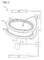
本開示の形態は、シリコン基板(例えばウエハ)のような半導体基板に応力を加える装置を含む。図1〜2を参照すると、装置11は、チャンバ31、および半導体基板49を保持するための基板サポート47を有する基板ホルダー20を含んでも良い。記載された装置11は、1つの基板を処理する装置であるが、ここに記載された装置および方法は、例えば複数の基板を処理する装置を含む他の装置での使用にも適している。 The embodiments of the present disclosure include an apparatus for applying stress to a semiconductor substrate such as a silicon substrate (for example, a wafer). With reference to FIGS. 1-2, the
装置は、基板に応力を加える「ストレッサ(stressor)」を含んでも良い。例えば、ストレッサまたはストレッサアセンブリは、1またはそれ以上のヒータ15または圧力変調器27を含んでも良い。ヒータ15は、以下で述べるように、基板ホルダー(またはホルダーの一部)とは異なる速度で基板を延ばすことで、基板に応力を加えることができる。代わりにまたは追加で、ストレッサは、基板を横切って差圧を分け与える圧力変調器27でも良い。それらは、単に、ストレッサの可能な幾つかの例であり、他もこの開示の範囲内であると考える。 The device may include a "stressor" that stresses the substrate. For example, the stressor or stressor assembly may include one or
装置11は、壁33により一部が規定された内部空間を有するチャンバ31を含む。チャンバ31の斜視図は、装置11をより良く示すために、チャンバ壁の一部が除去されて図2に示される。チャンバ31の内部空間の中に、半導体基板49を支持する基板ホルダー20がある。図1〜2に示されたホルダー20はサセプタ47であるが、他のホルダー配置(例えば、管、リング、クランプ等)も考えられ、それらの幾つかはより全体が以下に述べられる。基板ホルダーは、図1〜2では20で、図3〜34では、20プラス100の倍数(120、220、320等)で示される。 The
チャンバ31は、シャフト9または他の好適なサポートの上に載せられる。装置11、例えばシャフト9は、好適な制御バルブおよび/または水力または空気力のラインまたは張力ケーブル等のような、ホルダーに、基板49を掴みおよび/または放させるデバイスを含んでも良い。チャンバ31は、本開示の範囲から離れることなく、ここで示した配置とは異なる配置を含んでも良い。 The
基板ホルダーまたはホルダーの一部は、チャンバ31の上および下に配置された高強度の放射熱ランプのようなヒータ15により形成された放射熱光を吸収するために、ほぼ不透明でも良い。ホルダーは、炭化シリコンで覆われた不透明なグラファイトから形成されても良い。チャンバ31の壁は、透明な材料から形成され、放射熱光をチャンバ中に通しても良い。例えば、チャンバ31の壁は、透明な水晶から形成されても良い。水晶は、赤外光や可視光に対してほぼ透明で、一般的なプロセス温度において化学的に安定である。 The substrate holder or part of the holder may be substantially opaque in order to absorb the radiant heat formed by the
例えば抵抗ヒータおよび誘導ヒータのような、高強度ランプ以外のヒータ15が、チャンバ31に熱を供給するために使用されても良い。追加または代わりに、本開示の範囲から離れることなく、ヒータ15はチャンバ31の内部空間中に含まれても良く、またはチャンバ壁と一体でも良い。換言すれば、ヒータは、いずれの好適なタイプ、大きさ、および形状でも良く、チャンバの内部または外部に配置されても良い。パイロメータのような赤外温度センサ(図示せず)がチャンバ31の上に載置され、ホルダーまたは基板により放出される赤外放射を受けることにより、ホルダー20または基板49の温度をモニタしても良い。システムコントローラ(図1)は、例えばストレッサコントロール、ガス流速、およびチャンバの温度および圧力を含む、チャンバ31に関連する様々な操作パラメータを制御するために使用されても良い。図1〜2に示される以外の装置やチャンバ設計は、本開示の範囲から離れることなく使用しても良い。
所定の具体例では、装置11は半導体基板に応力を加えるのに適し、任意的に基板上にエピタキシャル層のような半導体材料を堆積するのに適した構造からなり、および/また構造を含んでも良い。そのような具体例では、半導体材料を含むプロセスガスは、ガスシリンダのようなプロセスガス源からガスマニフォールド(図示せず)およびチャンバ31の中へと、装置11の中に流れても良い。ガスは、プロセスの前、途中、または後に、チャンバに導入されても良い。ガスは、基板49に接触する前に加熱されても良い。半導体基板の表面上にエピタキシャル層を堆積するためのプロセスは、例えば、米国特許5,789,309、米国特許5,904,769、および米国特許5,769,942に記載されたような、公知の方法を含んでも良い。一般に、エピタキシャル層の成長は、化学気相堆積により達成される。一般的に言えば、化学気相堆積は、揮発性反応物を、キャリアガス(通常水素)を用いてチャンバ31内に導入することを含む。 In certain embodiments, the
半導体基板に応力を加えるための基板ホルダーの様々な具体例がここに記載される。半導体基板に応力を加えるための、基板ホルダーおよびストレッサ(例えばヒータ、圧力変調器等)の幾つかの代わりの具体例が以下に示されるが、この開示の範囲内で、他のホルダーおよびストレッサが考えられる。なお、ホルダーおよびストレッサは、上述の装置11およびチャンバ31の一部として使用されても良く、またはチャンバを加熱するためのヒータと組み合わせて使用しても良い。 Various specific examples of substrate holders for applying stress to semiconductor substrates are described here. Some alternative embodiments of substrate holders and stressors (eg, heaters, pressure modulators, etc.) for applying stress to semiconductor substrates are shown below, but within the scope of this disclosure, other holders and stressors Conceivable. The holder and stressor may be used as a part of the above-mentioned
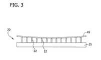
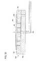
図3〜4を参照すると、基板ホルダー20は、半導体基板49を支持する、複数の、間隔をあけた細長いピン22を含んでも良い。ピン22は、載置ブロック25に取り付けられる。基板49に力が加えられ、基板を動かして(曲げて)、ピンに接触させても良い。ピン22、またはその上方部分は、曲げ位置(即ち加圧位置)で基板49に接触するために配置された支持面を選択的に規定しても良い。 With reference to FIGS. 3-4, the
ピン22、またはその上方部分は、凹状パターンに配置され、十分な力が加えられた場合に、実質的に平坦な形状から基板が変形または曲がり、ピンの凹型配置に一致しても良い。この方法で変形させることで、基板49は応力が加えられる。 The
他の具体例では、装置は図1(および以下の図7)に示すような圧力変調器を含み、基板に応力を加えるのに十分な基板を横切る差圧を形成する。他のストレッサは、他の具体例で使用されても良い。 In another embodiment, the device includes a pressure modulator as shown in FIG. 1 (and FIG. 7 below) to create a differential pressure across the substrate sufficient to stress the substrate. Other stressors may be used in other embodiments.
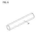
図5〜6に示すように、ピン22’は管状で、これにより液体のための管を形成する。いくつかの具体例では、ピン22”は、真空に引くためのポンプのような圧力変調器27に流体接続される。基板49に与えられた真空は、引力により、基板をピンに向かって引っ張っても良い。例えば、ピンの凹形パターンによるピンと基板との間の距離のばらつきは、基板の部分に、異なる量の引く力を与えても良い。異なる力は、半導体基板49に与えられる応力となる。 As shown in FIGS. 5-6, the pin 22'is tubular, which forms a tube for the liquid. In some embodiments, the
ピン22、22’は、一般に垂直方向に基板を支持するが、それらは、水平方向または変形方向の基板の移動を制限しないように形成されても良い。加熱中の基板の半径方向の移動を可能にすると、スリップや転位を引き起こすことなく、基板が半径方向に拡大されるようになる。以下に記載し図31〜35に示すように、ピンは、載置ブロック(からと言うよりむしろ)を通って延びて、ひと続きの導管を通って接続されても良い。 The
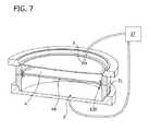
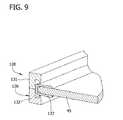
図7〜12を参照して、半導体基板を曲げるための装置の1つの具体例では、装置は、表リング131と裏リング132を有するホルダー120を含む。表リング131は、環状の表サポート134を含み、裏リング132は、環状の裏サポート136を含み、基板49に接触して支持する。なお、表リングと裏リングは、図8に示すようにL形状の断面を有しても良い、表リング131は、別個の半径位置で基板49の表面に接触するように取り付けられ、裏リング132は、別個の半径位置で基板49の裏面に接触するように取り付けられる。半径位置は、周縁からわずかに内方である。表の環状サポート134と裏の環状サポート136が基板49に接する半径方向の位置は、図8に示すように同じでも良く、または本開示の範囲から離れることなく異なっても良い。 In one embodiment of an apparatus for bending a semiconductor substrate with reference to FIGS. 7-12, the apparatus includes a
図10を参照すると、基板49を曲げるための装置(例えばストレッサ)は、ポンプのような圧力変調器27を含み、基板を横切って差圧を形成しても良い。換言すれば、圧力が、ウエハの一つの側で、他より高くなる。差圧は基板の応力を加え、基板を曲げても良い。そのような具体例では、表リング131と裏リング132は、シールとして働き、基板49を横切る差圧は維持される。圧力変調器27は、チャンバ31の壁を通って延びて、チャンバ内のキャビティ4をシールするベント3と、流体接続されても良い。基板49を横切って与えられる差圧は、より圧力の低い方向に基板を曲げても良い。 Referring to FIG. 10, the device for bending the substrate 49 (eg, a stressor) may include a
基板49の曲げにより、基板の表面は、表リング131と裏リング132との間で動いても良い。更に、基板49の熱膨張(即ち、リング131、132の熱膨張より大きな熱膨張)により、リング131、132の間で表面が動く。1つの具体例では、図9に示すように、保護コーティング137が基板49の一部を覆い、特に、基板の周縁を覆う。コーティング137は、一般に、基板がリング131、132の間に補正されると共に、(スリップや転位のような)ダメージからウエハを保護する保護材料でも良い。 By bending the
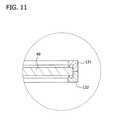
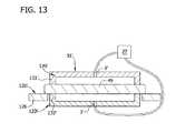
図13を参照して、ホルダー120’の表リング131’と裏リング132’は、リングが、装置120のリング131、132を有するような基板の周縁(図8)ではなく、その近傍で、基板49に接するように、配置されても良い。リング131’、132’は、チャンバ31’の蓋および/または底と一体でも良い。ベント3’は、チャンバ31’のリング131’、132’を通って延びても良い。ベント3’は、基板49の中央近傍に配置され、圧力変調器27が活性化した場合に、基板の変形を制限しても良い。 With reference to FIG. 13, the front ring 131'and the back ring 132' of the holder 120'are not at the periphery of the substrate (FIG. 8) such that the ring has the
ホルダー120’は、また、例えばリング131’、132’の適用前に、基板49を支持する平坦なサポート126を含んでも良い。所定の具体例では、基板49が平坦なサポート126に取り付けられる。平坦なサポートは、基板とは異なる熱膨張係数を有する材料から形成されて(即ち、リングは、基板とは異なる速度で熱膨張する)、サポートと基板が加熱または冷却された場合に、圧縮されまたは引っ張られても良い。 The holder 120'may also include a
図14を参照して、装置の幾つかの具体例では、装置は、基板の熱膨張の使用により基板49の上に応力を加える。基板ホルダー220は、基板49の上に保持力を加える表リング231および裏リング232を含むクランプ240を含んでも良い。表リング231は、環状の表サポート234を含み、裏リング232は、環状の裏サポート236を含む。サポート234、236は、基板の周縁において基板49と接触し、基板の表と裏にそれぞれ接触するように取り付けられる。例えば、図14に示す基板ホルダー220は、圧力モジュール無しに使用しても良い。なお、ここに記載される様々なホルダーのリング、サポート、ボス、クランプ等は、空気式、水圧式、モータ等の使用を含むいずれかの機械的方法により、半径方向に動かしても良い。 With reference to FIG. 14, in some specific examples of the device, the device applies stress onto the
リング231、232は、基板とは異なる熱膨張係数を有する材料から形成されても良い(即ち、リングは、基板とは異なる速度で熱膨張する)。加熱または冷却時の、リング231、232の異なる膨張速度と組み合わせたクランプ240の保持力は、基板459に応力を加える。リング231、232が、基板49より大きな膨張係数を有する具体例では、リングは基板を半径方向に引き延ばす。リング231、232が、基板49より小さい膨張係数を有する具体例では、リングは内方に向かう力を基板に加え(即ち、基板の圧縮)、基板を曲げる。 The
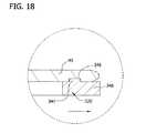
図15〜18を参照して、他の具体例では、基板ホルダー320は、おおむね平坦な裏サポート346を含み、これは、基板49の裏で、溝348に受けられる大きさおよび形状の環状のボスを含む。ボス347は、基板49の上に応力を加えるように移動可能である。例えば、裏サポート346は、加熱が基板を圧縮する場合、基板49よりも小さい速度で膨張する材料から形成されても良い。代わりに、裏サポート346は、加熱が基板を引っ張る場合、基板49よりも大きな速度で膨張する材料から形成されても良い。 With reference to FIGS. 15-18, in another embodiment, the
基板ホルダー320は、また、図8に示す表リング131および裏リング132と類似した環状のサポートを有する表リングおよび裏リング(図示せず)を含み、基板をシールして、基板に応力を加えるために圧力変調器が基板を横切る差圧を形成しても良い。ホルダー320を含むチャンバ31は、真空または圧力を与えるためのベント3およびシールされたキャビティ4を含んでも良い(図17)。裏リングは、裏サポート346の内側にあり、表リングは、裏リングと整列するか、または裏リングより基板の周縁に近くなる大きさおよび形状を有しても良い。基板は、図9に示すようなコーティングを含んでも良い。 The
幾つかの具体例では、図19〜21に示すように、基板ホルダー320は、また、表サポートから延びる環状リング352を有する表サポート350を含む。リング352は、基板49に下方に向かう力を加え、加熱中の基板の圧縮または膨張中に、ボス347から基板が外れるのを防止する。この機能を達成する他の構造は、本開示の範囲内にあるものと考える。 In some embodiments, as shown in FIGS. 19-21, the
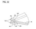
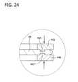
他の具体例および図22〜24に示すように、基板ホルダー420は、図15〜21に示すものと類似または同様の裏サポート446およびボス447を含む。基板ホルダー420は、表サポート451と、基板49の表面の溝457に受け入れられる大きさおよび形状の表ボス455を含んでも良い。表サポート451は、また、加熱が基板を圧縮した場合、基板49よりも小さい速度で膨張する材料から形成されても良く。または、加熱が基板を引っ張る場合、基板49よりも大きな速度で膨張する材料から形成されても良い。 As shown in other embodiments and FIGS. 22-24, the
図25〜27を参照して、この具値例の加圧装置520は、基板49を支持するための平坦な裏サポート561と、基板を受け入れて圧縮するための円形の開口部を有するおおむね円形のプレス560を含む。図26〜28のように、平坦なサポートは、部分的に基板の中心にのみ向かって延びるか、または基板49の真下に連続して延びても良い。プレス560は、基板を連続して囲んでも良く、または、図27に示すように、基板49を受け入れる開口部を形成する複数の円弧形状のセグメント563を含んでも良い。プレス560および/またはセグメント563は、基板を圧縮するために、基板49に対して内方に移動可能でも良い。例えば、プレス560は、基板49より小さな速度で膨張する材料から形成された結果、加熱した場合に、プレスは基板を圧縮するように動いても良い。基板ホルダー520は、また、表リングおよび/または裏リング(図示せず)を含み、上述のように、基板を横切る差圧を形成するためにシールを形成しても良い。 With reference to FIGS. 25-27, the pressurizing
図28を参照して、基板ホルダー620は、第1の円錐形状のサポート670と、第1の円錐形状のサポートと対向する第2の円錐形状のサポート675を含む。第1の円錐形状のサポート670は、孔を通って真空に引くための、そして第1の円錐形状のサポートに向かって基板49を引っ張るための、その中に形成された複数の孔671を含む。第1のサポート670の上方部分は、曲げない状態の、基板49の一部に接触する。上部部分より一般に大きく、真空に引くための孔671を含む下部部分678は、曲げ位置にある場合に、基板と接触する。ベント679は、第2のサポート675の中に形成され、このサポートは、基板に応力を加えるために、ベントとキャビティを通して引いて真空になるキャビティ672を形成する。環状のサポート675は、一般に、基板の周縁またはその近傍のみで、基板49に接触する。 With reference to FIG. 28, the
図29を参照して、基板ホルダー720は、おおよそ平坦な裏サポート781とフランジ783とを含む。基板49は、基板の周縁近傍で基板の裏面に取り付けられたリング780を含む。フランジ783は、リング780と噛み合うように取り付けられる。サポート781とフランジ783は、基板を圧縮するために、基板に対して移動可能である。例えば、サポート781および/またはフランジ783は、基板49より大きな速度で膨張する材料から形成された結果、加熱した場合に、フランジ783は基板を引っ張るように動いても良い。基板のリング780がフランジ783の内部にある具体例(図示せず)では、サポート781および/またはフランジ783は、基板49より小さい速度で膨張する材料から形成された結果、加熱した場合に、フランジ783は基板を圧縮するように動いても良い。 With reference to FIG. 29, the
図30は、基板ホルダー920の載置ブロック991の底部を示す。ひと続きの管989が載置ブロック991を通って凹形状のサポート992まで延びる(図32)。管989は、ひと続きの導管990を介して接続される。載置ブロック991は、処理チャンバ31(図1)に載置ブロックを挿入したり取り外したりするためのハンドリング溝993を含んでも良い。図32に示すように、載置ブロック991は、チャンバ中で、載置ブロックサポート994の上に支持されても良い。真空管996は、載置ブロックサポート994を通って延びて、チャンバ31(図1)の中に載置ブロックが挿入された場合、導管990および管989と流体接続する。基板49は、載置ブロック991の上に配置される(図33)、真空が適用された場合、基板49は凹形状のサポート992に向かって曲がり、基板に応力を加える(図34)。 FIG. 30 shows the bottom of the mounting
一般に、基板上の応力は、例えば図14〜27および29に示された装置の具体例を使用して、圧縮または引っ張る場合、基板の軸に対して直交する方向に向いても良い。代わりに、応力は、例えば図5、7〜13、28および30〜34に示された装置の具体例を使用して、基板の軸に沿ってまたは平行に向いても良い。 In general, stresses on a substrate may be directed in a direction orthogonal to the axis of the substrate when compressed or pulled, for example using the specific examples of the device shown in FIGS. 14-27 and 29. Alternatively, the stress may be directed along or parallel to the axis of the substrate, for example using the specific examples of the devices shown in FIGS. 5, 7-13, 28 and 30-34.
本開示またはその好適な具体例の要素を紹介する場合、冠詞「1つの(a)」、「1つの(an)」、「その(the)」、および「その(said)」は、1またはそれ以上の要素があることを意味する。「含む(comprising)」、「含む(including)」および「有する(having)」の用語は、包括的であることを意図し、列挙された要素の他に追加の要素があることを意味する。 When introducing the elements of the present disclosure or a preferred embodiment thereof, the articles "one (a)", "one (an)", "the", and "the" are 1 or It means that there are more elements. The terms "comprising," "inclusion," and "having" are intended to be comprehensive and mean that there are additional elements in addition to the listed elements.
上記装置および方法において、本開示の範囲から離れることなく、様々な変形が可能であるため、上記開示に含まれ、添付の図面に示された、全ての事項は、例示的で、限定する意図無しに解釈されるべきである。 All matters contained in the disclosure and shown in the accompanying drawings are exemplary and intended to be limiting, as the devices and methods are capable of various modifications without departing from the scope of the present disclosure. Should be interpreted without.
Claims (4)
Translated fromJapaneseし、この装置は、
チャンバと、
チャンバを加熱するためのヒータと、
チャンバ中に配置された基板ホルダーであって、このホルダーは空間を隔てた複数の細長いピンを含み、それぞれのピンは基板と接触するためのサポート面を有し、このサポート面は、曲げ位置にある基板に接触するために配置されており、それぞれのピンは、管状であり基板を真空引きする流体経路を有し、これらのピンは、ほぼ垂直方向に基板を支持するように構成され、基板加熱状態において基板が半径方向に拡大可能なように、ほぼ水平方向の基板の動きを可能にするように構成されている、基板ホルダーと、
基板を真空に引くためのポンプと、
を含むことを特徴とする装置。A device for bending a semiconductor substrate, the substrate has an almost flat position and a bending position, and this device is
With the chamber
A heater for heating the chamber and
A board holder placed in a chamber, the holder containing a plurality of elongated pins separated by space, each pin having a support surface for contact with the board, the support surface being in a bent position. is arranged to contact the one substrate, andeach pin is tubular substrate having a fluid path for evacuating the pinsisconfigured to support a substrate in a substantially vertical direction,the substrateA substrate holder and a substrate holder that are configured to allow movement of the substrate in a nearly horizontal directionso that the substrate can expand radially in the heated state.
A pump to evacuate the board,
A device characterized by including.
特徴とする請求項1に記載の装置。The apparatus accordingto claim 1, wherein the chamber is an epitaxial chamber for forming an epitaxial layer.
調器を含むことを特徴とする請求項1又は2に記載の装置。The apparatus accordingto claim 1 or 2 , further comprising a pressure modulator for forming a differential pressure across the substrate sufficient to apply stress on the substrate.
項1〜3のいずれかに記載の装置。The device according to any one ofclaims 1 to 3 , wherein at least some support surfaces of the pin have a pointed tip.
Applications Claiming Priority (8)
| Application Number | Priority Date | Filing Date | Title |
|---|---|---|---|
| US201261747613P | 2012-12-31 | 2012-12-31 | |
| US61/747,613 | 2012-12-31 | ||
| US201361788744P | 2013-03-15 | 2013-03-15 | |
| US201361790445P | 2013-03-15 | 2013-03-15 | |
| US201361793999P | 2013-03-15 | 2013-03-15 | |
| US61/788,744 | 2013-03-15 | ||
| US61/793,999 | 2013-03-15 | ||
| US61/790,445 | 2013-03-15 |
Related Parent Applications (1)
| Application Number | Title | Priority Date | Filing Date |
|---|---|---|---|
| JP2015550846ADivisionJP6314154B2 (en) | 2012-12-31 | 2013-12-30 | Equipment for applying stress to semiconductor substrates |
Related Child Applications (1)
| Application Number | Title | Priority Date | Filing Date |
|---|---|---|---|
| JP2019092835ADivisionJP6814841B2 (en) | 2012-12-31 | 2019-05-16 | A device that applies stress to a semiconductor substrate |
Publications (2)
| Publication Number | Publication Date |
|---|---|
| JP2018117130A JP2018117130A (en) | 2018-07-26 |
| JP6837019B2true JP6837019B2 (en) | 2021-03-03 |
Family
ID=49958756
Family Applications (10)
| Application Number | Title | Priority Date | Filing Date |
|---|---|---|---|
| JP2015550832AActiveJP6314153B2 (en) | 2012-12-31 | 2013-12-30 | Process and apparatus for preparing a heterostructure with reduced strain by radial expansion |
| JP2015550841AActiveJP6373868B2 (en) | 2012-12-31 | 2013-12-30 | Process and apparatus for preparing a heterostructure with reduced strain by radial compression |
| JP2015550846AActiveJP6314154B2 (en) | 2012-12-31 | 2013-12-30 | Equipment for applying stress to semiconductor substrates |
| JP2018023318AActiveJP6545842B2 (en) | 2012-12-31 | 2018-02-13 | Process and apparatus for preparing a heterostructure reduced in strain by radial expansion |
| JP2018023957AActiveJP6837019B2 (en) | 2012-12-31 | 2018-02-14 | A device that applies stress to a semiconductor substrate |
| JP2019092835AActiveJP6814841B2 (en) | 2012-12-31 | 2019-05-16 | A device that applies stress to a semiconductor substrate |
| JP2019113987AActiveJP6861242B2 (en) | 2012-12-31 | 2019-06-19 | Processes and equipment for preparing heterostructures with reduced strain due to radial expansion |
| JP2020187362AActiveJP7082654B2 (en) | 2012-12-31 | 2020-11-10 | A device that applies stress to a semiconductor substrate |
| JP2020203209AActiveJP7114681B2 (en) | 2012-12-31 | 2020-12-08 | A device that applies stress to a semiconductor substrate |
| JP2022119435APendingJP2022166859A (en) | 2012-12-31 | 2022-07-27 | A device that applies stress to a semiconductor substrate |
Family Applications Before (4)
| Application Number | Title | Priority Date | Filing Date |
|---|---|---|---|
| JP2015550832AActiveJP6314153B2 (en) | 2012-12-31 | 2013-12-30 | Process and apparatus for preparing a heterostructure with reduced strain by radial expansion |
| JP2015550841AActiveJP6373868B2 (en) | 2012-12-31 | 2013-12-30 | Process and apparatus for preparing a heterostructure with reduced strain by radial compression |
| JP2015550846AActiveJP6314154B2 (en) | 2012-12-31 | 2013-12-30 | Equipment for applying stress to semiconductor substrates |
| JP2018023318AActiveJP6545842B2 (en) | 2012-12-31 | 2018-02-13 | Process and apparatus for preparing a heterostructure reduced in strain by radial expansion |
Family Applications After (5)
| Application Number | Title | Priority Date | Filing Date |
|---|---|---|---|
| JP2019092835AActiveJP6814841B2 (en) | 2012-12-31 | 2019-05-16 | A device that applies stress to a semiconductor substrate |
| JP2019113987AActiveJP6861242B2 (en) | 2012-12-31 | 2019-06-19 | Processes and equipment for preparing heterostructures with reduced strain due to radial expansion |
| JP2020187362AActiveJP7082654B2 (en) | 2012-12-31 | 2020-11-10 | A device that applies stress to a semiconductor substrate |
| JP2020203209AActiveJP7114681B2 (en) | 2012-12-31 | 2020-12-08 | A device that applies stress to a semiconductor substrate |
| JP2022119435APendingJP2022166859A (en) | 2012-12-31 | 2022-07-27 | A device that applies stress to a semiconductor substrate |
Country Status (7)
| Country | Link |
|---|---|
| US (7) | US9583363B2 (en) |
| EP (6) | EP3188224B1 (en) |
| JP (10) | JP6314153B2 (en) |
| KR (2) | KR102203560B1 (en) |
| CN (5) | CN107968067B (en) |
| TW (4) | TWI673865B (en) |
| WO (3) | WO2014106177A1 (en) |
Families Citing this family (266)
| Publication number | Priority date | Publication date | Assignee | Title |
|---|---|---|---|---|
| US20130023129A1 (en) | 2011-07-20 | 2013-01-24 | Asm America, Inc. | Pressure transmitter for a semiconductor processing environment |
| US10714315B2 (en) | 2012-10-12 | 2020-07-14 | Asm Ip Holdings B.V. | Semiconductor reaction chamber showerhead |
| US9583363B2 (en)* | 2012-12-31 | 2017-02-28 | Sunedison Semiconductor Limited (Uen201334164H) | Processes and apparatus for preparing heterostructures with reduced strain by radial distension |
| US20160376700A1 (en) | 2013-02-01 | 2016-12-29 | Asm Ip Holding B.V. | System for treatment of deposition reactor |
| WO2014191624A1 (en)* | 2013-05-29 | 2014-12-04 | Beneq Oy | Substrate holder and arrangement for holding substrates |
| WO2014191621A1 (en)* | 2013-05-29 | 2014-12-04 | Beneq Oy | Substrate carrier and arrangement for supporting substrates |
| US10941490B2 (en) | 2014-10-07 | 2021-03-09 | Asm Ip Holding B.V. | Multiple temperature range susceptor, assembly, reactor and system including the susceptor, and methods of using the same |
| US10276355B2 (en) | 2015-03-12 | 2019-04-30 | Asm Ip Holding B.V. | Multi-zone reactor, system including the reactor, and method of using the same |
| US10458018B2 (en) | 2015-06-26 | 2019-10-29 | Asm Ip Holding B.V. | Structures including metal carbide material, devices including the structures, and methods of forming same |
| US10211308B2 (en) | 2015-10-21 | 2019-02-19 | Asm Ip Holding B.V. | NbMC layers |
| DE102015223807A1 (en)* | 2015-12-01 | 2017-06-01 | Siltronic Ag | Process for producing a semiconductor wafer with epitaxial layer in a deposition chamber, apparatus for producing an epitaxial-layer semiconductor wafer and semiconductor wafer with epitaxial layer |
| US11139308B2 (en) | 2015-12-29 | 2021-10-05 | Asm Ip Holding B.V. | Atomic layer deposition of III-V compounds to form V-NAND devices |
| US10529554B2 (en) | 2016-02-19 | 2020-01-07 | Asm Ip Holding B.V. | Method for forming silicon nitride film selectively on sidewalls or flat surfaces of trenches |
| US10343920B2 (en) | 2016-03-18 | 2019-07-09 | Asm Ip Holding B.V. | Aligned carbon nanotubes |
| US11453943B2 (en) | 2016-05-25 | 2022-09-27 | Asm Ip Holding B.V. | Method for forming carbon-containing silicon/metal oxide or nitride film by ALD using silicon precursor and hydrocarbon precursor |
| US10612137B2 (en) | 2016-07-08 | 2020-04-07 | Asm Ip Holdings B.V. | Organic reactants for atomic layer deposition |
| US9859151B1 (en) | 2016-07-08 | 2018-01-02 | Asm Ip Holding B.V. | Selective film deposition method to form air gaps |
| CN107623028B (en)* | 2016-07-13 | 2021-02-19 | 环球晶圆股份有限公司 | Semiconductor substrate and processing method thereof |
| US9887082B1 (en) | 2016-07-28 | 2018-02-06 | Asm Ip Holding B.V. | Method and apparatus for filling a gap |
| US9812320B1 (en) | 2016-07-28 | 2017-11-07 | Asm Ip Holding B.V. | Method and apparatus for filling a gap |
| CN109564868B (en)* | 2016-08-25 | 2023-04-04 | 日本瑞翁株式会社 | Plasma etching method |
| US11532757B2 (en) | 2016-10-27 | 2022-12-20 | Asm Ip Holding B.V. | Deposition of charge trapping layers |
| US10714350B2 (en) | 2016-11-01 | 2020-07-14 | ASM IP Holdings, B.V. | Methods for forming a transition metal niobium nitride film on a substrate by atomic layer deposition and related semiconductor device structures |
| KR102546317B1 (en) | 2016-11-15 | 2023-06-21 | 에이에스엠 아이피 홀딩 비.브이. | Gas supply unit and substrate processing apparatus including the same |
| KR102762543B1 (en) | 2016-12-14 | 2025-02-05 | 에이에스엠 아이피 홀딩 비.브이. | Substrate processing apparatus |
| US11581186B2 (en) | 2016-12-15 | 2023-02-14 | Asm Ip Holding B.V. | Sequential infiltration synthesis apparatus |
| US11447861B2 (en) | 2016-12-15 | 2022-09-20 | Asm Ip Holding B.V. | Sequential infiltration synthesis apparatus and a method of forming a patterned structure |
| US10269558B2 (en) | 2016-12-22 | 2019-04-23 | Asm Ip Holding B.V. | Method of forming a structure on a substrate |
| US10068787B2 (en)* | 2016-12-30 | 2018-09-04 | Sunpower Corporation | Bowing semiconductor wafers |
| US11390950B2 (en) | 2017-01-10 | 2022-07-19 | Asm Ip Holding B.V. | Reactor system and method to reduce residue buildup during a film deposition process |
| US10468261B2 (en) | 2017-02-15 | 2019-11-05 | Asm Ip Holding B.V. | Methods for forming a metallic film on a substrate by cyclical deposition and related semiconductor device structures |
| US10770286B2 (en) | 2017-05-08 | 2020-09-08 | Asm Ip Holdings B.V. | Methods for selectively forming a silicon nitride film on a substrate and related semiconductor device structures |
| KR102015336B1 (en)* | 2017-06-12 | 2019-08-28 | 삼성전자주식회사 | Method of reducing warpage of semiconductor package substrate and warpage reducer device |
| US12040200B2 (en) | 2017-06-20 | 2024-07-16 | Asm Ip Holding B.V. | Semiconductor processing apparatus and methods for calibrating a semiconductor processing apparatus |
| US11306395B2 (en) | 2017-06-28 | 2022-04-19 | Asm Ip Holding B.V. | Methods for depositing a transition metal nitride film on a substrate by atomic layer deposition and related deposition apparatus |
| KR20190009245A (en) | 2017-07-18 | 2019-01-28 | 에이에스엠 아이피 홀딩 비.브이. | Methods for forming a semiconductor device structure and related semiconductor device structures |
| US11374112B2 (en) | 2017-07-19 | 2022-06-28 | Asm Ip Holding B.V. | Method for depositing a group IV semiconductor and related semiconductor device structures |
| US10590535B2 (en) | 2017-07-26 | 2020-03-17 | Asm Ip Holdings B.V. | Chemical treatment, deposition and/or infiltration apparatus and method for using the same |
| TWI815813B (en) | 2017-08-04 | 2023-09-21 | 荷蘭商Asm智慧財產控股公司 | Showerhead assembly for distributing a gas within a reaction chamber |
| US10692741B2 (en) | 2017-08-08 | 2020-06-23 | Asm Ip Holdings B.V. | Radiation shield |
| US10770336B2 (en) | 2017-08-08 | 2020-09-08 | Asm Ip Holding B.V. | Substrate lift mechanism and reactor including same |
| US11769682B2 (en) | 2017-08-09 | 2023-09-26 | Asm Ip Holding B.V. | Storage apparatus for storing cassettes for substrates and processing apparatus equipped therewith |
| US11830730B2 (en) | 2017-08-29 | 2023-11-28 | Asm Ip Holding B.V. | Layer forming method and apparatus |
| US11295980B2 (en) | 2017-08-30 | 2022-04-05 | Asm Ip Holding B.V. | Methods for depositing a molybdenum metal film over a dielectric surface of a substrate by a cyclical deposition process and related semiconductor device structures |
| US10658205B2 (en) | 2017-09-28 | 2020-05-19 | Asm Ip Holdings B.V. | Chemical dispensing apparatus and methods for dispensing a chemical to a reaction chamber |
| US10403504B2 (en) | 2017-10-05 | 2019-09-03 | Asm Ip Holding B.V. | Method for selectively depositing a metallic film on a substrate |
| US10923344B2 (en) | 2017-10-30 | 2021-02-16 | Asm Ip Holding B.V. | Methods for forming a semiconductor structure and related semiconductor structures |
| WO2019103613A1 (en) | 2017-11-27 | 2019-05-31 | Asm Ip Holding B.V. | A storage device for storing wafer cassettes for use with a batch furnace |
| CN111344522B (en) | 2017-11-27 | 2022-04-12 | 阿斯莫Ip控股公司 | Including clean mini-environment device |
| US10872771B2 (en) | 2018-01-16 | 2020-12-22 | Asm Ip Holding B. V. | Method for depositing a material film on a substrate within a reaction chamber by a cyclical deposition process and related device structures |
| TWI799494B (en) | 2018-01-19 | 2023-04-21 | 荷蘭商Asm 智慧財產控股公司 | Deposition method |
| KR102695659B1 (en) | 2018-01-19 | 2024-08-14 | 에이에스엠 아이피 홀딩 비.브이. | Method for depositing a gap filling layer by plasma assisted deposition |
| US11081345B2 (en) | 2018-02-06 | 2021-08-03 | Asm Ip Holding B.V. | Method of post-deposition treatment for silicon oxide film |
| US10896820B2 (en) | 2018-02-14 | 2021-01-19 | Asm Ip Holding B.V. | Method for depositing a ruthenium-containing film on a substrate by a cyclical deposition process |
| WO2019158960A1 (en) | 2018-02-14 | 2019-08-22 | Asm Ip Holding B.V. | A method for depositing a ruthenium-containing film on a substrate by a cyclical deposition process |
| US10731249B2 (en) | 2018-02-15 | 2020-08-04 | Asm Ip Holding B.V. | Method of forming a transition metal containing film on a substrate by a cyclical deposition process, a method for supplying a transition metal halide compound to a reaction chamber, and related vapor deposition apparatus |
| KR102636427B1 (en) | 2018-02-20 | 2024-02-13 | 에이에스엠 아이피 홀딩 비.브이. | Substrate processing method and apparatus |
| US10975470B2 (en) | 2018-02-23 | 2021-04-13 | Asm Ip Holding B.V. | Apparatus for detecting or monitoring for a chemical precursor in a high temperature environment |
| US11473195B2 (en) | 2018-03-01 | 2022-10-18 | Asm Ip Holding B.V. | Semiconductor processing apparatus and a method for processing a substrate |
| US11629406B2 (en) | 2018-03-09 | 2023-04-18 | Asm Ip Holding B.V. | Semiconductor processing apparatus comprising one or more pyrometers for measuring a temperature of a substrate during transfer of the substrate |
| KR102646467B1 (en) | 2018-03-27 | 2024-03-11 | 에이에스엠 아이피 홀딩 비.브이. | Method of forming an electrode on a substrate and a semiconductor device structure including an electrode |
| US11230766B2 (en) | 2018-03-29 | 2022-01-25 | Asm Ip Holding B.V. | Substrate processing apparatus and method |
| KR102600229B1 (en) | 2018-04-09 | 2023-11-10 | 에이에스엠 아이피 홀딩 비.브이. | Substrate supporting device, substrate processing apparatus including the same and substrate processing method |
| US12025484B2 (en) | 2018-05-08 | 2024-07-02 | Asm Ip Holding B.V. | Thin film forming method |
| TWI811348B (en) | 2018-05-08 | 2023-08-11 | 荷蘭商Asm 智慧財產控股公司 | Methods for depositing an oxide film on a substrate by a cyclical deposition process and related device structures |
| US12272527B2 (en) | 2018-05-09 | 2025-04-08 | Asm Ip Holding B.V. | Apparatus for use with hydrogen radicals and method of using same |
| KR102596988B1 (en) | 2018-05-28 | 2023-10-31 | 에이에스엠 아이피 홀딩 비.브이. | Method of processing a substrate and a device manufactured by the same |
| US11201079B2 (en)* | 2018-05-30 | 2021-12-14 | Taiwan Semiconductor Manufacturing Company, Ltd. | Wafer chuck |
| US11718913B2 (en) | 2018-06-04 | 2023-08-08 | Asm Ip Holding B.V. | Gas distribution system and reactor system including same |
| TWI840362B (en) | 2018-06-04 | 2024-05-01 | 荷蘭商Asm Ip私人控股有限公司 | Wafer handling chamber with moisture reduction |
| US11286562B2 (en) | 2018-06-08 | 2022-03-29 | Asm Ip Holding B.V. | Gas-phase chemical reactor and method of using same |
| KR102568797B1 (en) | 2018-06-21 | 2023-08-21 | 에이에스엠 아이피 홀딩 비.브이. | Substrate processing system |
| US10797133B2 (en) | 2018-06-21 | 2020-10-06 | Asm Ip Holding B.V. | Method for depositing a phosphorus doped silicon arsenide film and related semiconductor device structures |
| KR102854019B1 (en) | 2018-06-27 | 2025-09-02 | 에이에스엠 아이피 홀딩 비.브이. | Periodic deposition method for forming a metal-containing material and films and structures comprising the metal-containing material |
| TWI873894B (en) | 2018-06-27 | 2025-02-21 | 荷蘭商Asm Ip私人控股有限公司 | Cyclic deposition methods for forming metal-containing material and films and structures including the metal-containing material |
| US10612136B2 (en) | 2018-06-29 | 2020-04-07 | ASM IP Holding, B.V. | Temperature-controlled flange and reactor system including same |
| US10755922B2 (en) | 2018-07-03 | 2020-08-25 | Asm Ip Holding B.V. | Method for depositing silicon-free carbon-containing film as gap-fill layer by pulse plasma-assisted deposition |
| US10388513B1 (en) | 2018-07-03 | 2019-08-20 | Asm Ip Holding B.V. | Method for depositing silicon-free carbon-containing film as gap-fill layer by pulse plasma-assisted deposition |
| US11430674B2 (en) | 2018-08-22 | 2022-08-30 | Asm Ip Holding B.V. | Sensor array, apparatus for dispensing a vapor phase reactant to a reaction chamber and related methods |
| US11024523B2 (en) | 2018-09-11 | 2021-06-01 | Asm Ip Holding B.V. | Substrate processing apparatus and method |
| KR102707956B1 (en) | 2018-09-11 | 2024-09-19 | 에이에스엠 아이피 홀딩 비.브이. | Method for deposition of a thin film |
| CN110970344B (en) | 2018-10-01 | 2024-10-25 | Asmip控股有限公司 | Substrate holding apparatus, system comprising the same and method of using the same |
| US11232963B2 (en) | 2018-10-03 | 2022-01-25 | Asm Ip Holding B.V. | Substrate processing apparatus and method |
| KR102592699B1 (en) | 2018-10-08 | 2023-10-23 | 에이에스엠 아이피 홀딩 비.브이. | Substrate support unit and apparatuses for depositing thin film and processing the substrate including the same |
| KR102546322B1 (en) | 2018-10-19 | 2023-06-21 | 에이에스엠 아이피 홀딩 비.브이. | Substrate processing apparatus and substrate processing method |
| KR102605121B1 (en) | 2018-10-19 | 2023-11-23 | 에이에스엠 아이피 홀딩 비.브이. | Substrate processing apparatus and substrate processing method |
| US12378665B2 (en) | 2018-10-26 | 2025-08-05 | Asm Ip Holding B.V. | High temperature coatings for a preclean and etch apparatus and related methods |
| US11087997B2 (en) | 2018-10-31 | 2021-08-10 | Asm Ip Holding B.V. | Substrate processing apparatus for processing substrates |
| KR102748291B1 (en) | 2018-11-02 | 2024-12-31 | 에이에스엠 아이피 홀딩 비.브이. | Substrate support unit and substrate processing apparatus including the same |
| US11572620B2 (en) | 2018-11-06 | 2023-02-07 | Asm Ip Holding B.V. | Methods for selectively depositing an amorphous silicon film on a substrate |
| US10818758B2 (en) | 2018-11-16 | 2020-10-27 | Asm Ip Holding B.V. | Methods for forming a metal silicate film on a substrate in a reaction chamber and related semiconductor device structures |
| US12040199B2 (en) | 2018-11-28 | 2024-07-16 | Asm Ip Holding B.V. | Substrate processing apparatus for processing substrates |
| US11217444B2 (en) | 2018-11-30 | 2022-01-04 | Asm Ip Holding B.V. | Method for forming an ultraviolet radiation responsive metal oxide-containing film |
| KR102636428B1 (en) | 2018-12-04 | 2024-02-13 | 에이에스엠 아이피 홀딩 비.브이. | A method for cleaning a substrate processing apparatus |
| US11158513B2 (en) | 2018-12-13 | 2021-10-26 | Asm Ip Holding B.V. | Methods for forming a rhenium-containing film on a substrate by a cyclical deposition process and related semiconductor device structures |
| TWI874340B (en) | 2018-12-14 | 2025-03-01 | 荷蘭商Asm Ip私人控股有限公司 | Method of forming device structure, structure formed by the method and system for performing the method |
| TWI866480B (en) | 2019-01-17 | 2024-12-11 | 荷蘭商Asm Ip 私人控股有限公司 | Methods of forming a transition metal containing film on a substrate by a cyclical deposition process |
| KR102727227B1 (en) | 2019-01-22 | 2024-11-07 | 에이에스엠 아이피 홀딩 비.브이. | Semiconductor processing device |
| TWI838458B (en)* | 2019-02-20 | 2024-04-11 | 荷蘭商Asm Ip私人控股有限公司 | Apparatus and methods for plug fill deposition in 3-d nand applications |
| TWI845607B (en) | 2019-02-20 | 2024-06-21 | 荷蘭商Asm Ip私人控股有限公司 | Cyclical deposition method and apparatus for filling a recess formed within a substrate surface |
| KR102626263B1 (en) | 2019-02-20 | 2024-01-16 | 에이에스엠 아이피 홀딩 비.브이. | Cyclical deposition method including treatment step and apparatus for same |
| TWI873122B (en) | 2019-02-20 | 2025-02-21 | 荷蘭商Asm Ip私人控股有限公司 | Method of filling a recess formed within a surface of a substrate, semiconductor structure formed according to the method, and semiconductor processing apparatus |
| TWI842826B (en) | 2019-02-22 | 2024-05-21 | 荷蘭商Asm Ip私人控股有限公司 | Substrate processing apparatus and method for processing substrate |
| KR102858005B1 (en) | 2019-03-08 | 2025-09-09 | 에이에스엠 아이피 홀딩 비.브이. | Method for Selective Deposition of Silicon Nitride Layer and Structure Including Selectively-Deposited Silicon Nitride Layer |
| US11742198B2 (en) | 2019-03-08 | 2023-08-29 | Asm Ip Holding B.V. | Structure including SiOCN layer and method of forming same |
| KR102673983B1 (en)* | 2019-03-15 | 2024-06-12 | 주식회사 케이씨텍 | Apparatus for Treating Substrate |
| JP7279465B2 (en)* | 2019-03-28 | 2023-05-23 | 住友金属鉱山株式会社 | SUPPORTING SUBSTRATE, SUPPORTING SUBSTRATE HOLDING METHOD, AND FILM-FORMING METHOD |
| JP2020167398A (en) | 2019-03-28 | 2020-10-08 | エーエスエム・アイピー・ホールディング・ベー・フェー | Door openers and substrate processing equipment provided with door openers |
| KR102809999B1 (en) | 2019-04-01 | 2025-05-19 | 에이에스엠 아이피 홀딩 비.브이. | Method of manufacturing semiconductor device |
| KR20200123380A (en) | 2019-04-19 | 2020-10-29 | 에이에스엠 아이피 홀딩 비.브이. | Layer forming method and apparatus |
| KR20200125453A (en) | 2019-04-24 | 2020-11-04 | 에이에스엠 아이피 홀딩 비.브이. | Gas-phase reactor system and method of using same |
| KR20200130121A (en) | 2019-05-07 | 2020-11-18 | 에이에스엠 아이피 홀딩 비.브이. | Chemical source vessel with dip tube |
| US11289326B2 (en) | 2019-05-07 | 2022-03-29 | Asm Ip Holding B.V. | Method for reforming amorphous carbon polymer film |
| KR20200130652A (en) | 2019-05-10 | 2020-11-19 | 에이에스엠 아이피 홀딩 비.브이. | Method of depositing material onto a surface and structure formed according to the method |
| JP7612342B2 (en) | 2019-05-16 | 2025-01-14 | エーエスエム・アイピー・ホールディング・ベー・フェー | Wafer boat handling apparatus, vertical batch furnace and method |
| JP7598201B2 (en) | 2019-05-16 | 2024-12-11 | エーエスエム・アイピー・ホールディング・ベー・フェー | Wafer boat handling apparatus, vertical batch furnace and method |
| USD975665S1 (en) | 2019-05-17 | 2023-01-17 | Asm Ip Holding B.V. | Susceptor shaft |
| USD947913S1 (en) | 2019-05-17 | 2022-04-05 | Asm Ip Holding B.V. | Susceptor shaft |
| KR20200141002A (en) | 2019-06-06 | 2020-12-17 | 에이에스엠 아이피 홀딩 비.브이. | Method of using a gas-phase reactor system including analyzing exhausted gas |
| KR20200141931A (en) | 2019-06-10 | 2020-12-21 | 에이에스엠 아이피 홀딩 비.브이. | Method for cleaning quartz epitaxial chambers |
| KR20200143254A (en) | 2019-06-11 | 2020-12-23 | 에이에스엠 아이피 홀딩 비.브이. | Method of forming an electronic structure using an reforming gas, system for performing the method, and structure formed using the method |
| USD944946S1 (en) | 2019-06-14 | 2022-03-01 | Asm Ip Holding B.V. | Shower plate |
| KR20210005515A (en) | 2019-07-03 | 2021-01-14 | 에이에스엠 아이피 홀딩 비.브이. | Temperature control assembly for substrate processing apparatus and method of using same |
| JP7499079B2 (en) | 2019-07-09 | 2024-06-13 | エーエスエム・アイピー・ホールディング・ベー・フェー | Plasma device using coaxial waveguide and substrate processing method |
| CN112216646A (en) | 2019-07-10 | 2021-01-12 | Asm Ip私人控股有限公司 | Substrate supporting assembly and substrate processing device comprising same |
| KR20210010307A (en) | 2019-07-16 | 2021-01-27 | 에이에스엠 아이피 홀딩 비.브이. | Substrate processing apparatus |
| KR102860110B1 (en) | 2019-07-17 | 2025-09-16 | 에이에스엠 아이피 홀딩 비.브이. | Methods of forming silicon germanium structures |
| KR20210010816A (en) | 2019-07-17 | 2021-01-28 | 에이에스엠 아이피 홀딩 비.브이. | Radical assist ignition plasma system and method |
| US11643724B2 (en) | 2019-07-18 | 2023-05-09 | Asm Ip Holding B.V. | Method of forming structures using a neutral beam |
| TWI839544B (en) | 2019-07-19 | 2024-04-21 | 荷蘭商Asm Ip私人控股有限公司 | Method of forming topology-controlled amorphous carbon polymer film |
| KR20210010817A (en) | 2019-07-19 | 2021-01-28 | 에이에스엠 아이피 홀딩 비.브이. | Method of Forming Topology-Controlled Amorphous Carbon Polymer Film |
| TWI851767B (en) | 2019-07-29 | 2024-08-11 | 荷蘭商Asm Ip私人控股有限公司 | Methods for selective deposition utilizing n-type dopants and/or alternative dopants to achieve high dopant incorporation |
| CN112309900A (en) | 2019-07-30 | 2021-02-02 | Asm Ip私人控股有限公司 | Substrate processing apparatus |
| CN112309899A (en) | 2019-07-30 | 2021-02-02 | Asm Ip私人控股有限公司 | Substrate processing apparatus |
| US12169361B2 (en) | 2019-07-30 | 2024-12-17 | Asm Ip Holding B.V. | Substrate processing apparatus and method |
| US11587815B2 (en) | 2019-07-31 | 2023-02-21 | Asm Ip Holding B.V. | Vertical batch furnace assembly |
| US11227782B2 (en) | 2019-07-31 | 2022-01-18 | Asm Ip Holding B.V. | Vertical batch furnace assembly |
| US11587814B2 (en) | 2019-07-31 | 2023-02-21 | Asm Ip Holding B.V. | Vertical batch furnace assembly |
| CN112323048B (en) | 2019-08-05 | 2024-02-09 | Asm Ip私人控股有限公司 | Liquid level sensor for chemical source container |
| CN112342526A (en) | 2019-08-09 | 2021-02-09 | Asm Ip私人控股有限公司 | Heater assembly including cooling device and method of using same |
| USD965524S1 (en) | 2019-08-19 | 2022-10-04 | Asm Ip Holding B.V. | Susceptor support |
| USD965044S1 (en) | 2019-08-19 | 2022-09-27 | Asm Ip Holding B.V. | Susceptor shaft |
| JP2021031769A (en) | 2019-08-21 | 2021-03-01 | エーエスエム アイピー ホールディング ビー.ブイ. | Production apparatus of mixed gas of film deposition raw material and film deposition apparatus |
| USD979506S1 (en) | 2019-08-22 | 2023-02-28 | Asm Ip Holding B.V. | Insulator |
| KR20210024423A (en) | 2019-08-22 | 2021-03-05 | 에이에스엠 아이피 홀딩 비.브이. | Method for forming a structure with a hole |
| USD949319S1 (en) | 2019-08-22 | 2022-04-19 | Asm Ip Holding B.V. | Exhaust duct |
| USD940837S1 (en) | 2019-08-22 | 2022-01-11 | Asm Ip Holding B.V. | Electrode |
| KR20210024420A (en) | 2019-08-23 | 2021-03-05 | 에이에스엠 아이피 홀딩 비.브이. | Method for depositing silicon oxide film having improved quality by peald using bis(diethylamino)silane |
| US11286558B2 (en) | 2019-08-23 | 2022-03-29 | Asm Ip Holding B.V. | Methods for depositing a molybdenum nitride film on a surface of a substrate by a cyclical deposition process and related semiconductor device structures including a molybdenum nitride film |
| KR102806450B1 (en) | 2019-09-04 | 2025-05-12 | 에이에스엠 아이피 홀딩 비.브이. | Methods for selective deposition using a sacrificial capping layer |
| KR102733104B1 (en) | 2019-09-05 | 2024-11-22 | 에이에스엠 아이피 홀딩 비.브이. | Substrate processing apparatus |
| US11562901B2 (en) | 2019-09-25 | 2023-01-24 | Asm Ip Holding B.V. | Substrate processing method |
| CN112593212B (en) | 2019-10-02 | 2023-12-22 | Asm Ip私人控股有限公司 | Method for forming topologically selective silicon oxide film by cyclic plasma enhanced deposition process |
| TWI846953B (en) | 2019-10-08 | 2024-07-01 | 荷蘭商Asm Ip私人控股有限公司 | Substrate processing device |
| KR20210042810A (en) | 2019-10-08 | 2021-04-20 | 에이에스엠 아이피 홀딩 비.브이. | Reactor system including a gas distribution assembly for use with activated species and method of using same |
| TW202128273A (en) | 2019-10-08 | 2021-08-01 | 荷蘭商Asm Ip私人控股有限公司 | Gas injection system, reactor system, and method of depositing material on surface of substratewithin reaction chamber |
| TWI846966B (en) | 2019-10-10 | 2024-07-01 | 荷蘭商Asm Ip私人控股有限公司 | Method of forming a photoresist underlayer and structure including same |
| US12009241B2 (en) | 2019-10-14 | 2024-06-11 | Asm Ip Holding B.V. | Vertical batch furnace assembly with detector to detect cassette |
| TWI834919B (en) | 2019-10-16 | 2024-03-11 | 荷蘭商Asm Ip私人控股有限公司 | Method of topology-selective film formation of silicon oxide |
| US11637014B2 (en) | 2019-10-17 | 2023-04-25 | Asm Ip Holding B.V. | Methods for selective deposition of doped semiconductor material |
| KR102845724B1 (en) | 2019-10-21 | 2025-08-13 | 에이에스엠 아이피 홀딩 비.브이. | Apparatus and methods for selectively etching films |
| US11328944B2 (en)* | 2019-10-23 | 2022-05-10 | Eugenus, Inc. | Systems and methods of placing substrates in semiconductor manufacturing equipment |
| KR20210050453A (en) | 2019-10-25 | 2021-05-07 | 에이에스엠 아이피 홀딩 비.브이. | Methods for filling a gap feature on a substrate surface and related semiconductor structures |
| US11646205B2 (en) | 2019-10-29 | 2023-05-09 | Asm Ip Holding B.V. | Methods of selectively forming n-type doped material on a surface, systems for selectively forming n-type doped material, and structures formed using same |
| KR20210054983A (en) | 2019-11-05 | 2021-05-14 | 에이에스엠 아이피 홀딩 비.브이. | Structures with doped semiconductor layers and methods and systems for forming same |
| US11501968B2 (en) | 2019-11-15 | 2022-11-15 | Asm Ip Holding B.V. | Method for providing a semiconductor device with silicon filled gaps |
| KR102861314B1 (en) | 2019-11-20 | 2025-09-17 | 에이에스엠 아이피 홀딩 비.브이. | Method of depositing carbon-containing material on a surface of a substrate, structure formed using the method, and system for forming the structure |
| US11450529B2 (en) | 2019-11-26 | 2022-09-20 | Asm Ip Holding B.V. | Methods for selectively forming a target film on a substrate comprising a first dielectric surface and a second metallic surface |
| CN112951697B (en) | 2019-11-26 | 2025-07-29 | Asmip私人控股有限公司 | Substrate processing apparatus |
| CN112885692B (en) | 2019-11-29 | 2025-08-15 | Asmip私人控股有限公司 | Substrate processing apparatus |
| CN120432376A (en) | 2019-11-29 | 2025-08-05 | Asm Ip私人控股有限公司 | Substrate processing apparatus |
| JP7527928B2 (en) | 2019-12-02 | 2024-08-05 | エーエスエム・アイピー・ホールディング・ベー・フェー | Substrate processing apparatus and substrate processing method |
| KR20210070898A (en) | 2019-12-04 | 2021-06-15 | 에이에스엠 아이피 홀딩 비.브이. | Substrate processing apparatus |
| KR20210078405A (en) | 2019-12-17 | 2021-06-28 | 에이에스엠 아이피 홀딩 비.브이. | Method of forming vanadium nitride layer and structure including the vanadium nitride layer |
| KR20210080214A (en) | 2019-12-19 | 2021-06-30 | 에이에스엠 아이피 홀딩 비.브이. | Methods for filling a gap feature on a substrate and related semiconductor structures |
| JP7730637B2 (en) | 2020-01-06 | 2025-08-28 | エーエスエム・アイピー・ホールディング・ベー・フェー | Gas delivery assembly, components thereof, and reactor system including same |
| JP7636892B2 (en) | 2020-01-06 | 2025-02-27 | エーエスエム・アイピー・ホールディング・ベー・フェー | Channeled Lift Pins |
| US11993847B2 (en) | 2020-01-08 | 2024-05-28 | Asm Ip Holding B.V. | Injector |
| KR20210093163A (en) | 2020-01-16 | 2021-07-27 | 에이에스엠 아이피 홀딩 비.브이. | Method of forming high aspect ratio features |
| US11791192B2 (en)* | 2020-01-19 | 2023-10-17 | Taiwan Semiconductor Manufacturing Company, Ltd. | Workpiece holder, wafer chuck, wafer holding method |
| KR102675856B1 (en) | 2020-01-20 | 2024-06-17 | 에이에스엠 아이피 홀딩 비.브이. | Method of forming thin film and method of modifying surface of thin film |
| TWI889744B (en) | 2020-01-29 | 2025-07-11 | 荷蘭商Asm Ip私人控股有限公司 | Contaminant trap system, and baffle plate stack |
| TW202513845A (en) | 2020-02-03 | 2025-04-01 | 荷蘭商Asm Ip私人控股有限公司 | Semiconductor structures and methods for forming the same |
| KR20210100010A (en) | 2020-02-04 | 2021-08-13 | 에이에스엠 아이피 홀딩 비.브이. | Method and apparatus for transmittance measurements of large articles |
| US11776846B2 (en) | 2020-02-07 | 2023-10-03 | Asm Ip Holding B.V. | Methods for depositing gap filling fluids and related systems and devices |
| KR20210103956A (en) | 2020-02-13 | 2021-08-24 | 에이에스엠 아이피 홀딩 비.브이. | Substrate processing apparatus including light receiving device and calibration method of light receiving device |
| TW202146691A (en) | 2020-02-13 | 2021-12-16 | 荷蘭商Asm Ip私人控股有限公司 | Gas distribution assembly, shower plate assembly, and method of adjusting conductance of gas to reaction chamber |
| TWI855223B (en) | 2020-02-17 | 2024-09-11 | 荷蘭商Asm Ip私人控股有限公司 | Method for growing phosphorous-doped silicon layer |
| CN113410160A (en) | 2020-02-28 | 2021-09-17 | Asm Ip私人控股有限公司 | System specially used for cleaning parts |
| KR20210113043A (en) | 2020-03-04 | 2021-09-15 | 에이에스엠 아이피 홀딩 비.브이. | Alignment fixture for a reactor system |
| US11876356B2 (en) | 2020-03-11 | 2024-01-16 | Asm Ip Holding B.V. | Lockout tagout assembly and system and method of using same |
| KR20210116240A (en) | 2020-03-11 | 2021-09-27 | 에이에스엠 아이피 홀딩 비.브이. | Substrate handling device with adjustable joints |
| KR102775390B1 (en) | 2020-03-12 | 2025-02-28 | 에이에스엠 아이피 홀딩 비.브이. | Method for Fabricating Layer Structure Having Target Topological Profile |
| US12173404B2 (en) | 2020-03-17 | 2024-12-24 | Asm Ip Holding B.V. | Method of depositing epitaxial material, structure formed using the method, and system for performing the method |
| KR102755229B1 (en) | 2020-04-02 | 2025-01-14 | 에이에스엠 아이피 홀딩 비.브이. | Thin film forming method |
| TWI887376B (en) | 2020-04-03 | 2025-06-21 | 荷蘭商Asm Ip私人控股有限公司 | Method for manufacturing semiconductor device |
| TWI888525B (en) | 2020-04-08 | 2025-07-01 | 荷蘭商Asm Ip私人控股有限公司 | Apparatus and methods for selectively etching silcon oxide films |
| KR20210127620A (en) | 2020-04-13 | 2021-10-22 | 에이에스엠 아이피 홀딩 비.브이. | method of forming a nitrogen-containing carbon film and system for performing the method |
| KR20210128343A (en) | 2020-04-15 | 2021-10-26 | 에이에스엠 아이피 홀딩 비.브이. | Method of forming chromium nitride layer and structure including the chromium nitride layer |
| US11821078B2 (en) | 2020-04-15 | 2023-11-21 | Asm Ip Holding B.V. | Method for forming precoat film and method for forming silicon-containing film |
| US11996289B2 (en) | 2020-04-16 | 2024-05-28 | Asm Ip Holding B.V. | Methods of forming structures including silicon germanium and silicon layers, devices formed using the methods, and systems for performing the methods |
| KR20210130646A (en) | 2020-04-21 | 2021-11-01 | 에이에스엠 아이피 홀딩 비.브이. | Method for processing a substrate |
| KR20210132600A (en) | 2020-04-24 | 2021-11-04 | 에이에스엠 아이피 홀딩 비.브이. | Methods and systems for depositing a layer comprising vanadium, nitrogen, and a further element |
| TW202208671A (en) | 2020-04-24 | 2022-03-01 | 荷蘭商Asm Ip私人控股有限公司 | Methods of forming structures including vanadium boride and vanadium phosphide layers |
| CN113555279A (en) | 2020-04-24 | 2021-10-26 | Asm Ip私人控股有限公司 | Methods of forming vanadium nitride-containing layers and structures comprising the same |
| KR20210132612A (en) | 2020-04-24 | 2021-11-04 | 에이에스엠 아이피 홀딩 비.브이. | Methods and apparatus for stabilizing vanadium compounds |
| KR102866804B1 (en) | 2020-04-24 | 2025-09-30 | 에이에스엠 아이피 홀딩 비.브이. | Vertical batch furnace assembly comprising a cooling gas supply |
| KR102783898B1 (en) | 2020-04-29 | 2025-03-18 | 에이에스엠 아이피 홀딩 비.브이. | Solid source precursor vessel |
| KR20210134869A (en) | 2020-05-01 | 2021-11-11 | 에이에스엠 아이피 홀딩 비.브이. | Fast FOUP swapping with a FOUP handler |
| JP7726664B2 (en) | 2020-05-04 | 2025-08-20 | エーエスエム・アイピー・ホールディング・ベー・フェー | Substrate processing system for processing a substrate |
| KR20210137395A (en) | 2020-05-07 | 2021-11-17 | 에이에스엠 아이피 홀딩 비.브이. | Apparatus and methods for performing an in-situ etch of reaction chambers with fluorine-based radicals |
| KR102788543B1 (en) | 2020-05-13 | 2025-03-27 | 에이에스엠 아이피 홀딩 비.브이. | Laser alignment fixture for a reactor system |
| TW202146699A (en) | 2020-05-15 | 2021-12-16 | 荷蘭商Asm Ip私人控股有限公司 | Method of forming a silicon germanium layer, semiconductor structure, semiconductor device, method of forming a deposition layer, and deposition system |
| KR20210143653A (en) | 2020-05-19 | 2021-11-29 | 에이에스엠 아이피 홀딩 비.브이. | Substrate processing apparatus |
| KR20210145079A (en) | 2020-05-21 | 2021-12-01 | 에이에스엠 아이피 홀딩 비.브이. | Flange and apparatus for processing substrates |
| KR102795476B1 (en) | 2020-05-21 | 2025-04-11 | 에이에스엠 아이피 홀딩 비.브이. | Structures including multiple carbon layers and methods of forming and using same |
| TWI873343B (en) | 2020-05-22 | 2025-02-21 | 荷蘭商Asm Ip私人控股有限公司 | Reaction system for forming thin film on substrate |
| KR20210146802A (en) | 2020-05-26 | 2021-12-06 | 에이에스엠 아이피 홀딩 비.브이. | Method for depositing boron and gallium containing silicon germanium layers |
| TWI876048B (en) | 2020-05-29 | 2025-03-11 | 荷蘭商Asm Ip私人控股有限公司 | Substrate processing device |
| TW202212620A (en) | 2020-06-02 | 2022-04-01 | 荷蘭商Asm Ip私人控股有限公司 | Apparatus for processing substrate, method of forming film, and method of controlling apparatus for processing substrate |
| TW202208659A (en) | 2020-06-16 | 2022-03-01 | 荷蘭商Asm Ip私人控股有限公司 | Method for depositing boron containing silicon germanium layers |
| TW202218133A (en) | 2020-06-24 | 2022-05-01 | 荷蘭商Asm Ip私人控股有限公司 | Method for forming a layer provided with silicon |
| TWI873359B (en) | 2020-06-30 | 2025-02-21 | 荷蘭商Asm Ip私人控股有限公司 | Substrate processing method |
| US12431354B2 (en) | 2020-07-01 | 2025-09-30 | Asm Ip Holding B.V. | Silicon nitride and silicon oxide deposition methods using fluorine inhibitor |
| TW202202649A (en) | 2020-07-08 | 2022-01-16 | 荷蘭商Asm Ip私人控股有限公司 | Substrate processing method |
| KR20220010438A (en) | 2020-07-17 | 2022-01-25 | 에이에스엠 아이피 홀딩 비.브이. | Structures and methods for use in photolithography |
| TWI878570B (en) | 2020-07-20 | 2025-04-01 | 荷蘭商Asm Ip私人控股有限公司 | Method and system for depositing molybdenum layers |
| KR20220011092A (en) | 2020-07-20 | 2022-01-27 | 에이에스엠 아이피 홀딩 비.브이. | Method and system for forming structures including transition metal layers |
| US12322591B2 (en) | 2020-07-27 | 2025-06-03 | Asm Ip Holding B.V. | Thin film deposition process |
| KR20220021863A (en) | 2020-08-14 | 2022-02-22 | 에이에스엠 아이피 홀딩 비.브이. | Method for processing a substrate |
| US12040177B2 (en) | 2020-08-18 | 2024-07-16 | Asm Ip Holding B.V. | Methods for forming a laminate film by cyclical plasma-enhanced deposition processes |
| TW202228863A (en) | 2020-08-25 | 2022-08-01 | 荷蘭商Asm Ip私人控股有限公司 | Method for cleaning a substrate, method for selectively depositing, and reaction system |
| US11725280B2 (en) | 2020-08-26 | 2023-08-15 | Asm Ip Holding B.V. | Method for forming metal silicon oxide and metal silicon oxynitride layers |
| TW202229601A (en) | 2020-08-27 | 2022-08-01 | 荷蘭商Asm Ip私人控股有限公司 | Method of forming patterned structures, method of manipulating mechanical property, device structure, and substrate processing system |
| TW202217045A (en) | 2020-09-10 | 2022-05-01 | 荷蘭商Asm Ip私人控股有限公司 | Methods for depositing gap filing fluids and related systems and devices |
| USD990534S1 (en) | 2020-09-11 | 2023-06-27 | Asm Ip Holding B.V. | Weighted lift pin |
| KR20220036866A (en) | 2020-09-16 | 2022-03-23 | 에이에스엠 아이피 홀딩 비.브이. | Silicon oxide deposition method |
| USD1012873S1 (en) | 2020-09-24 | 2024-01-30 | Asm Ip Holding B.V. | Electrode for semiconductor processing apparatus |
| TWI889903B (en) | 2020-09-25 | 2025-07-11 | 荷蘭商Asm Ip私人控股有限公司 | Semiconductor processing method |
| US12009224B2 (en) | 2020-09-29 | 2024-06-11 | Asm Ip Holding B.V. | Apparatus and method for etching metal nitrides |
| KR20220045900A (en) | 2020-10-06 | 2022-04-13 | 에이에스엠 아이피 홀딩 비.브이. | Deposition method and an apparatus for depositing a silicon-containing material |
| CN114293174A (en) | 2020-10-07 | 2022-04-08 | Asm Ip私人控股有限公司 | Gas supply unit and substrate processing apparatus including the same |
| TW202229613A (en) | 2020-10-14 | 2022-08-01 | 荷蘭商Asm Ip私人控股有限公司 | Method of depositing material on stepped structure |
| TW202232565A (en) | 2020-10-15 | 2022-08-16 | 荷蘭商Asm Ip私人控股有限公司 | Method of manufacturing semiconductor device, and substrate treatment apparatus using ether-cat |
| TW202217037A (en) | 2020-10-22 | 2022-05-01 | 荷蘭商Asm Ip私人控股有限公司 | Method of depositing vanadium metal, structure, device and a deposition assembly |
| TW202223136A (en) | 2020-10-28 | 2022-06-16 | 荷蘭商Asm Ip私人控股有限公司 | Method for forming layer on substrate, and semiconductor processing system |
| TW202229620A (en) | 2020-11-12 | 2022-08-01 | 特文特大學 | Deposition system, method for controlling reaction condition, method for depositing |
| TW202229795A (en) | 2020-11-23 | 2022-08-01 | 荷蘭商Asm Ip私人控股有限公司 | A substrate processing apparatus with an injector |
| TW202235649A (en) | 2020-11-24 | 2022-09-16 | 荷蘭商Asm Ip私人控股有限公司 | Methods for filling a gap and related systems and devices |
| TW202235675A (en) | 2020-11-30 | 2022-09-16 | 荷蘭商Asm Ip私人控股有限公司 | Injector, and substrate processing apparatus |
| US12255053B2 (en) | 2020-12-10 | 2025-03-18 | Asm Ip Holding B.V. | Methods and systems for depositing a layer |
| TW202233884A (en) | 2020-12-14 | 2022-09-01 | 荷蘭商Asm Ip私人控股有限公司 | Method of forming structures for threshold voltage control |
| US11946137B2 (en) | 2020-12-16 | 2024-04-02 | Asm Ip Holding B.V. | Runout and wobble measurement fixtures |
| TW202232639A (en) | 2020-12-18 | 2022-08-16 | 荷蘭商Asm Ip私人控股有限公司 | Wafer processing apparatus with a rotatable table |
| TW202226899A (en) | 2020-12-22 | 2022-07-01 | 荷蘭商Asm Ip私人控股有限公司 | Plasma treatment device having matching box |
| TW202242184A (en) | 2020-12-22 | 2022-11-01 | 荷蘭商Asm Ip私人控股有限公司 | Precursor capsule, precursor vessel, vapor deposition assembly, and method of loading solid precursor into precursor vessel |
| TW202231903A (en) | 2020-12-22 | 2022-08-16 | 荷蘭商Asm Ip私人控股有限公司 | Transition metal deposition method, transition metal layer, and deposition assembly for depositing transition metal on substrate |
| USD1023959S1 (en) | 2021-05-11 | 2024-04-23 | Asm Ip Holding B.V. | Electrode for substrate processing apparatus |
| USD980813S1 (en) | 2021-05-11 | 2023-03-14 | Asm Ip Holding B.V. | Gas flow control plate for substrate processing apparatus |
| USD980814S1 (en) | 2021-05-11 | 2023-03-14 | Asm Ip Holding B.V. | Gas distributor for substrate processing apparatus |
| USD981973S1 (en) | 2021-05-11 | 2023-03-28 | Asm Ip Holding B.V. | Reactor wall for substrate processing apparatus |
| JP2023031456A (en)* | 2021-08-25 | 2023-03-09 | 日本特殊陶業株式会社 | Substrate holding member and manufacturing method for the same |
| USD990441S1 (en) | 2021-09-07 | 2023-06-27 | Asm Ip Holding B.V. | Gas flow control plate |
| USD1060598S1 (en) | 2021-12-03 | 2025-02-04 | Asm Ip Holding B.V. | Split showerhead cover |
| US20240035161A1 (en)* | 2022-07-26 | 2024-02-01 | Applied Materials, Inc. | Actively controlled pre-heat ring for process temperature control |
| CN119177489B (en)* | 2023-06-21 | 2025-07-04 | 上海天岳半导体材料有限公司 | SiC substrate and SiC crystal with uniform stress distribution in three-dimensional direction |
Family Cites Families (131)
| Publication number | Priority date | Publication date | Assignee | Title |
|---|---|---|---|---|
| JPS54112164A (en) | 1978-02-22 | 1979-09-01 | Nec Home Electronics Ltd | Manufacture of semiconductor device |
| JPS54134564A (en) | 1978-04-12 | 1979-10-19 | Hitachi Ltd | Wafer dividing unit |
| DE3110341C2 (en) | 1980-03-19 | 1983-11-17 | Hitachi, Ltd., Tokyo | Method and apparatus for aligning a thin substrate in the image plane of a copier |
| US4473455A (en) | 1981-12-21 | 1984-09-25 | At&T Bell Laboratories | Wafer holding apparatus and method |
| JPS59117235A (en) | 1982-12-24 | 1984-07-06 | Hitachi Yonezawa Denshi Kk | Wafer breaking method and device |
| US4542298A (en)* | 1983-06-09 | 1985-09-17 | Varian Associates, Inc. | Methods and apparatus for gas-assisted thermal transfer with a semiconductor wafer |
| US4704886A (en)* | 1985-04-22 | 1987-11-10 | Aluminum Company Of America | Stretch-forming process |
| JPH0697674B2 (en)* | 1986-02-19 | 1994-11-30 | キヤノン株式会社 | Ball contact type wafer chuck |
| JPS62284707A (en) | 1986-06-03 | 1987-12-10 | セイコーエプソン株式会社 | Wafer breaking device |
| US4842683A (en)* | 1986-12-19 | 1989-06-27 | Applied Materials, Inc. | Magnetic field-enhanced plasma etch reactor |
| US5096536A (en)* | 1990-06-12 | 1992-03-17 | Micron Technology, Inc. | Method and apparatus useful in the plasma etching of semiconductor materials |
| DE4024576A1 (en)* | 1990-08-02 | 1992-02-06 | Bosch Gmbh Robert | DEVICE FOR SINGLE-SIDED ASSEMBLY OF A SEMICONDUCTOR DISC |
| KR0164618B1 (en)* | 1992-02-13 | 1999-02-01 | 이노우에 쥰이치 | Plasma process method using an electrostatic chuck |
| US5343012A (en) | 1992-10-06 | 1994-08-30 | Hardy Walter N | Differentially pumped temperature controller for low pressure thin film fabrication process |
| US5326725A (en)* | 1993-03-11 | 1994-07-05 | Applied Materials, Inc. | Clamping ring and susceptor therefor |
| JPH0897159A (en) | 1994-09-29 | 1996-04-12 | Handotai Process Kenkyusho:Kk | Method and system for epitaxial growth |
| US5868847A (en) | 1994-12-16 | 1999-02-09 | Applied Materials, Inc. | Clamp ring for shielding a substrate during film layer deposition |
| JPH08176798A (en) | 1994-12-27 | 1996-07-09 | Idoutai Tsushin Sentan Gijutsu Kenkyusho:Kk | Functional thin film manufacturing method |
| JP3220619B2 (en) | 1995-05-24 | 2001-10-22 | 松下電器産業株式会社 | Gas heat transfer plasma processing equipment |
| US5618759A (en) | 1995-05-31 | 1997-04-08 | Texas Instruments Incorporated | Methods of and apparatus for immobilizing semiconductor wafers during sawing thereof |
| EP1050602B1 (en)* | 1995-08-03 | 2004-05-26 | ASM America, Inc. | Process chamber with inner support |
| US6093252A (en) | 1995-08-03 | 2000-07-25 | Asm America, Inc. | Process chamber with inner support |
| JP3865803B2 (en)* | 1995-08-29 | 2007-01-10 | 株式会社半導体エネルギー研究所 | Optical processing method and method for manufacturing semiconductor device |
| JP3180208B2 (en) | 1995-09-18 | 2001-06-25 | 株式会社新川 | Pellet pickup device |
| JPH0992625A (en) | 1995-09-20 | 1997-04-04 | Tokyo Electron Ltd | Boat for heat treatment |
| JP3477953B2 (en) | 1995-10-18 | 2003-12-10 | 東京エレクトロン株式会社 | Heat treatment equipment |
| JP3725598B2 (en) | 1996-01-12 | 2005-12-14 | 東芝セラミックス株式会社 | Epitaxial wafer manufacturing method |
| US6133550A (en)* | 1996-03-22 | 2000-10-17 | Sandia Corporation | Method and apparatus for thermal processing of semiconductor substrates |
| US5753566A (en) | 1996-05-23 | 1998-05-19 | Taiwan Semiconductor Manufactured Company, Ltd. | Method of spin-on-glass etchback using hot backside helium |
| JPH10106907A (en) | 1996-10-01 | 1998-04-24 | Canon Inc | Solid phase joining method |
| US5789309A (en) | 1996-12-30 | 1998-08-04 | Memc Electronic Materials, Inc. | Method and system for monocrystalline epitaxial deposition |
| JP3347742B2 (en)* | 1997-01-02 | 2002-11-20 | シーヴイシー・プロダクツ・インコーポレーテッド | Heat conductive chuck for vacuum processing device, heat transfer device, and method for transferring heat between chuck body and substrate |
| US5936829A (en) | 1997-01-02 | 1999-08-10 | Cvc Products, Inc. | Thermally conductive chuck for vacuum processor |
| JP3257442B2 (en) | 1997-04-09 | 2002-02-18 | 松下電器産業株式会社 | Method for producing gallium nitride crystal |
| US6113479A (en)* | 1997-07-25 | 2000-09-05 | Obsidian, Inc. | Wafer carrier for chemical mechanical planarization polishing |
| JPH1154437A (en)* | 1997-07-30 | 1999-02-26 | Kyocera Corp | Method for forming compound semiconductor film |
| JP3662404B2 (en) | 1997-11-19 | 2005-06-22 | 芝浦メカトロニクス株式会社 | Wafer sheet stretching apparatus and pellet bonding apparatus using the same |
| JPH11154662A (en)* | 1997-11-20 | 1999-06-08 | Seiko Instruments Inc | Semiconductor manufacture device |
| DE19802977A1 (en)* | 1998-01-27 | 1999-07-29 | Forschungszentrum Juelich Gmbh | Single crystal layer production on a non-lattice-matched single crystal substrate in microelectronic or optoelectronics component manufacture |
| JPH11240795A (en) | 1998-02-27 | 1999-09-07 | Super Silicon Kenkyusho:Kk | Epitaxial growth apparatus |
| JP3178517B2 (en) | 1998-03-05 | 2001-06-18 | 日本電気株式会社 | Sample stage for pattern exposure equipment |
| CN1063224C (en)* | 1998-06-16 | 2001-03-14 | 中国科学院化工冶金研究所 | Airlift cyclic immersion lighting plant cell tissue organ culture method and culture reactor |
| JP2000031253A (en) | 1998-07-10 | 2000-01-28 | Komatsu Ltd | Substrate processing apparatus and method |
| JP3544481B2 (en)* | 1998-11-25 | 2004-07-21 | 東芝セラミックス株式会社 | Silicon carbide assembly wafer boat for semiconductor manufacturing |
| US6277198B1 (en)* | 1999-06-04 | 2001-08-21 | Applied Materials, Inc. | Use of tapered shadow clamp ring to provide improved physical vapor deposition system |
| US6513848B1 (en) | 1999-09-17 | 2003-02-04 | Applied Materials, Inc. | Hydraulically actuated wafer clamp |
| US6191399B1 (en) | 2000-02-01 | 2001-02-20 | Asm America, Inc. | System of controlling the temperature of a processing chamber |
| US6726537B1 (en)* | 2000-04-21 | 2004-04-27 | Agere Systems Inc. | Polishing carrier head |
| KR20010111058A (en)* | 2000-06-09 | 2001-12-15 | 조셉 제이. 스위니 | Full area temperature controlled electrostatic chuck and method of fabricating same |
| EP1184894B1 (en)* | 2000-08-29 | 2007-11-21 | Qimonda Dresden GmbH & Co. oHG | Method of operating a susceptor for semiconductor wafers |
| TWI303084B (en) | 2000-09-08 | 2008-11-11 | Tokyo Electron Ltd | Shower head structure, film forming method, and gas processing apparauts |
| KR100382491B1 (en)* | 2000-11-28 | 2003-05-09 | 엘지전자 주식회사 | shadow mask in organic electroluminescence |
| US6649480B2 (en) | 2000-12-04 | 2003-11-18 | Amberwave Systems Corporation | Method of fabricating CMOS inverter and integrated circuits utilizing strained silicon surface channel MOSFETs |
| FR2818254B1 (en) | 2000-12-15 | 2003-02-28 | Immunotech Sa | PACKAGING FOR PHOTOSENSITIVE COLORANTS |
| DE10111761A1 (en)* | 2001-03-12 | 2002-10-02 | Infineon Technologies Ag | Arrangement and method for contacting a semiconductor substrate from the rear |
| US6855037B2 (en)* | 2001-03-12 | 2005-02-15 | Asm-Nutool, Inc. | Method of sealing wafer backside for full-face electrochemical plating |
| US6743495B2 (en) | 2001-03-30 | 2004-06-01 | Memc Electronic Materials, Inc. | Thermal annealing process for producing silicon wafers with improved surface characteristics |
| US6855649B2 (en)* | 2001-06-12 | 2005-02-15 | International Business Machines Corporation | Relaxed SiGe layers on Si or silicon-on-insulator substrates by ion implantation and thermal annealing |
| JP2004533125A (en)* | 2001-06-22 | 2004-10-28 | エムイーエムシー・エレクトロニック・マテリアルズ・インコーポレイテッド | Method of fabricating a silicon-on-insulator structure having intrinsic gettering by ion implantation |
| TW554069B (en)* | 2001-08-10 | 2003-09-21 | Ebara Corp | Plating device and method |
| US6743296B2 (en) | 2001-10-12 | 2004-06-01 | Taiwan Semiconductor Manufacturing Co., Ltd | Apparatus and method for self-centering a wafer in a sputter chamber |
| JP2003204048A (en)* | 2002-01-09 | 2003-07-18 | Shin Etsu Handotai Co Ltd | Method for manufacturing soi wafer and soi wafer |
| JP2003234289A (en) | 2002-02-12 | 2003-08-22 | Yoshihisa Hirose | Manufacturing method of strain mitigating film, and laminate having strain mitigating film |
| KR100995715B1 (en)* | 2002-04-09 | 2010-11-19 | 파나소닉 주식회사 | Plasma treatment method and apparatus and plasma treatment tray |
| US20030209326A1 (en) | 2002-05-07 | 2003-11-13 | Mattson Technology, Inc. | Process and system for heating semiconductor substrates in a processing chamber containing a susceptor |
| JP2004146727A (en)* | 2002-10-28 | 2004-05-20 | Tokyo Seimitsu Co Ltd | Transferring method of wafer |
| CN100568101C (en) | 2002-11-12 | 2009-12-09 | Asml荷兰有限公司 | Photolithography apparatus and device manufacturing method |
| JP2004179452A (en) | 2002-11-28 | 2004-06-24 | Shin Etsu Handotai Co Ltd | Hetero epitaxial wafer |
| US7972663B2 (en) | 2002-12-20 | 2011-07-05 | Applied Materials, Inc. | Method and apparatus for forming a high quality low temperature silicon nitride layer |
| JP4487306B2 (en) | 2003-03-17 | 2010-06-23 | Toto株式会社 | Composite structure forming apparatus and forming method |
| JP4325242B2 (en)* | 2003-03-27 | 2009-09-02 | 富士電機デバイステクノロジー株式会社 | Manufacturing method of semiconductor device |
| DE10318284A1 (en) | 2003-04-22 | 2004-11-25 | Forschungszentrum Jülich GmbH | Process for producing a strained layer on a substrate and layer structure |
| JP2004342819A (en) | 2003-05-15 | 2004-12-02 | Toshiba Ceramics Co Ltd | Semiconductor substrate and method of manufacturing the same |
| JP4557505B2 (en) | 2003-05-19 | 2010-10-06 | コバレントマテリアル株式会社 | Manufacturing method of semiconductor substrate |
| US7223320B2 (en) | 2003-06-12 | 2007-05-29 | Symbol Technologies, Inc. | Method and apparatus for expanding a semiconductor wafer |
| US6951775B2 (en)* | 2003-06-28 | 2005-10-04 | International Business Machines Corporation | Method for forming interconnects on thin wafers |
| US20050178336A1 (en) | 2003-07-15 | 2005-08-18 | Heng Liu | Chemical vapor deposition reactor having multiple inlets |
| US7439158B2 (en)* | 2003-07-21 | 2008-10-21 | Micron Technology, Inc. | Strained semiconductor by full wafer bonding |
| US7824498B2 (en) | 2004-02-24 | 2010-11-02 | Applied Materials, Inc. | Coating for reducing contamination of substrates during processing |
| JP2006080481A (en)* | 2004-08-11 | 2006-03-23 | Canon Inc | Semiconductor substrate and manufacturing method thereof |
| WO2006033292A1 (en)* | 2004-09-24 | 2006-03-30 | Shin-Etsu Handotai Co., Ltd. | Method for manufacturing semiconductor wafer |
| US7273800B2 (en) | 2004-11-01 | 2007-09-25 | International Business Machines Corporation | Hetero-integrated strained silicon n- and p-MOSFETs |
| JP2006237262A (en)* | 2005-02-24 | 2006-09-07 | Tokyo Electron Ltd | Heat treatment apparatus |
| US7642205B2 (en) | 2005-04-08 | 2010-01-05 | Mattson Technology, Inc. | Rapid thermal processing using energy transfer layers |
| JP4666473B2 (en)* | 2005-05-12 | 2011-04-06 | 大日本スクリーン製造株式会社 | Substrate heat treatment equipment |
| JP5050374B2 (en) | 2005-05-16 | 2012-10-17 | 富士電機株式会社 | Manufacturing method of semiconductor device |
| US7262112B2 (en)* | 2005-06-27 | 2007-08-28 | The Regents Of The University Of California | Method for producing dislocation-free strained crystalline films |
| US20070049020A1 (en)* | 2005-08-29 | 2007-03-01 | Applied Materials, Inc. | Method and apparatus for reducing tensile stress in a deposited layer |
| EP1763069B1 (en)* | 2005-09-07 | 2016-04-13 | Soitec | Method for forming a semiconductor heterostructure |
| US20080000579A1 (en)* | 2005-11-08 | 2008-01-03 | Giovanni Bortolato | Procedure and Equipment for Decoration of Objects by Sublimation Inks |
| TWI276535B (en)* | 2005-12-07 | 2007-03-21 | Nano Prec Corp | Film attaching method and screen of rear projection television |
| JP4851795B2 (en)* | 2006-01-13 | 2012-01-11 | 株式会社ディスコ | Wafer divider |
| JP2007214199A (en) | 2006-02-07 | 2007-08-23 | Canon Inc | Semiconductor substrate and manufacturing method thereof |
| US20070283884A1 (en)* | 2006-05-30 | 2007-12-13 | Applied Materials, Inc. | Ring assembly for substrate processing chamber |
| EP1901345A1 (en) | 2006-08-30 | 2008-03-19 | Siltronic AG | Multilayered semiconductor wafer and process for manufacturing the same |
| DE102006055038B4 (en)* | 2006-11-22 | 2012-12-27 | Siltronic Ag | An epitaxated semiconductor wafer and apparatus and method for producing an epitaxied semiconductor wafer |
| US8580078B2 (en) | 2007-01-26 | 2013-11-12 | Lam Research Corporation | Bevel etcher with vacuum chuck |
| JP2008198656A (en) | 2007-02-08 | 2008-08-28 | Shin Etsu Chem Co Ltd | Manufacturing method of semiconductor substrate |
| US7732301B1 (en) | 2007-04-20 | 2010-06-08 | Pinnington Thomas Henry | Bonded intermediate substrate and method of making same |
| JP2009016524A (en) | 2007-07-04 | 2009-01-22 | Rohm Co Ltd | Thin film forming apparatus and ZnO-based thin film |
| WO2009020024A1 (en)* | 2007-08-03 | 2009-02-12 | Shin-Etsu Handotai Co., Ltd. | Susceptor and method for manufacturing silicon epitaxial wafer |
| JP2009135430A (en)* | 2007-10-10 | 2009-06-18 | Semiconductor Energy Lab Co Ltd | Method for manufacturing semiconductor device |
| WO2009060913A1 (en) | 2007-11-08 | 2009-05-14 | Sumco Corporation | Method for manufacturing epitaxial wafer |
| JP5370850B2 (en) | 2007-11-08 | 2013-12-18 | 株式会社Sumco | Epitaxial film growth method, wafer support structure, and susceptor |
| TW200935506A (en)* | 2007-11-16 | 2009-08-16 | Panasonic Corp | Plasma dicing apparatus and semiconductor chip manufacturing method |
| EP2151852B1 (en) | 2008-08-06 | 2020-01-15 | Soitec | Relaxation and transfer of strained layers |
| US8652260B2 (en)* | 2008-08-08 | 2014-02-18 | Taiwan Semiconductor Manufacturing Company, Ltd. | Apparatus for holding semiconductor wafers |
| JP2010073782A (en)* | 2008-09-17 | 2010-04-02 | Sumco Corp | Method of heat-treating semiconductor wafer |
| KR20100108418A (en)* | 2008-11-14 | 2010-10-06 | 도쿄엘렉트론가부시키가이샤 | Bonding apparatus and bonding method |
| JP5161748B2 (en) | 2008-12-16 | 2013-03-13 | 信越半導体株式会社 | Vapor growth susceptor, vapor growth apparatus, and epitaxial wafer manufacturing method |
| DE102009005182A1 (en) | 2009-01-15 | 2010-07-29 | Suss Microtec Test Systems Gmbh | Chuck and method for holding and holding thin test substrates |
| IT1392678B1 (en) | 2009-01-19 | 2012-03-16 | Valeo Spa | SAFETY DEVICE FOR VEHICLE HANDLES AND VEHICLE HANDLE INCLUDING THIS SAFETY DEVICE |
| JP5476006B2 (en) | 2009-02-13 | 2014-04-23 | 株式会社国際電気セミコンダクターサービス | SUBSTRATE PROCESSING APPARATUS, SUBSTRATE HOLDER FIXING UNIT OF SUBSTRATE PROCESSING APPARATUS, AND SEMICONDUCTOR DEVICE MANUFACTURING METHOD |
| JP2010189745A (en) | 2009-02-20 | 2010-09-02 | Sumco Corp | Method of manufacturing semiconductor wafer |
| JP2011029303A (en) | 2009-07-23 | 2011-02-10 | Panasonic Corp | Semiconductor device and method of manufacturing the same |
| JP2011035146A (en) | 2009-07-31 | 2011-02-17 | Toppan Printing Co Ltd | Substrate holding method and substrate processing device |
| JP5480645B2 (en)* | 2010-01-22 | 2014-04-23 | リンテック株式会社 | Support frame |
| US8747092B2 (en)* | 2010-01-22 | 2014-06-10 | Nanonex Corporation | Fast nanoimprinting apparatus using deformale mold |
| JP5627649B2 (en) | 2010-09-07 | 2014-11-19 | 株式会社東芝 | Method for manufacturing nitride semiconductor crystal layer |
| JP5810517B2 (en) | 2010-12-02 | 2015-11-11 | 富士電機株式会社 | Adsorption device and adsorption method |
| JP5605264B2 (en)* | 2011-02-23 | 2014-10-15 | 富士通株式会社 | Film forming method and film forming apparatus |
| CN103443901B (en)* | 2011-03-28 | 2017-09-15 | 应用材料公司 | Method and apparatus for selectively depositing epitaxial germanium alloy stressors |
| KR20120119781A (en) | 2011-04-22 | 2012-10-31 | 삼성전자주식회사 | Unit for suppporting a substrate and apparatus for treating a substrate with the unit |
| TWI564982B (en)* | 2011-04-26 | 2017-01-01 | 尼康股份有限公司 | A substrate holding device, a substrate bonding device, a substrate holding method, a substrate bonding method, a laminated semiconductor device, and a laminated substrate |
| US8397540B2 (en)* | 2011-05-05 | 2013-03-19 | Corning Incorporated | Methods and apparatus for reforming a glass sheet |
| US9224904B1 (en) | 2011-07-24 | 2015-12-29 | Ananda Kumar | Composite substrates of silicon and ceramic |
| JP5895676B2 (en)* | 2012-04-09 | 2016-03-30 | 三菱電機株式会社 | Manufacturing method of semiconductor device |
| US20140239529A1 (en)* | 2012-09-28 | 2014-08-28 | Nanonex Corporation | System and Methods For Nano-Scale Manufacturing |
| US9583363B2 (en)* | 2012-12-31 | 2017-02-28 | Sunedison Semiconductor Limited (Uen201334164H) | Processes and apparatus for preparing heterostructures with reduced strain by radial distension |
| US9230862B2 (en)* | 2013-05-14 | 2016-01-05 | Texas Instruments Incorporated | Wafer die separation |
| EP3611572B1 (en)* | 2013-06-28 | 2023-04-05 | Nikon Corporation | Mobile body apparatus, exposure apparatus, and device manufacturing method |
- 2013
- 2013-12-27USUS14/142,553patent/US9583363B2/enactiveActive
- 2013-12-27USUS14/142,559patent/US10361097B2/enactiveActive
- 2013-12-27USUS14/142,556patent/US9583364B2/enactiveActive
- 2013-12-30CNCN201810030851.9Apatent/CN107968067B/enactiveActive
- 2013-12-30EPEP17154584.1Apatent/EP3188224B1/enactiveActive
- 2013-12-30EPEP13821774.0Apatent/EP2939258B1/enactiveActive
- 2013-12-30KRKR1020157020443Apatent/KR102203560B1/enactiveActive
- 2013-12-30CNCN201380073273.2Apatent/CN105210172B/enactiveActive
- 2013-12-30JPJP2015550832Apatent/JP6314153B2/enactiveActive
- 2013-12-30EPEP17154585.8Apatent/EP3185278B1/enactiveActive
- 2013-12-30CNCN201380073264.3Apatent/CN105144341B/enactiveActive
- 2013-12-30KRKR1020157020444Apatent/KR102224422B1/enactiveActive
- 2013-12-30CNCN202310507878.3Apatent/CN116544172A/enactivePending
- 2013-12-30EPEP13821770.8Apatent/EP2939257B1/enactiveActive
- 2013-12-30JPJP2015550841Apatent/JP6373868B2/enactiveActive
- 2013-12-30WOPCT/US2013/078295patent/WO2014106177A1/enactiveApplication Filing
- 2013-12-30CNCN201810287918.7Apatent/CN108336013B/enactiveActive
- 2013-12-30WOPCT/US2013/078329patent/WO2014106190A2/enactiveApplication Filing
- 2013-12-30JPJP2015550846Apatent/JP6314154B2/enactiveActive
- 2013-12-30EPEP18193203.9Apatent/EP3435406B1/enactiveActive
- 2013-12-30EPEP21214435.6Apatent/EP4002429B1/enactiveActive
- 2013-12-30WOPCT/US2013/078224patent/WO2014106155A2/enactiveApplication Filing
- 2013-12-31TWTW107118490Apatent/TWI673865B/enactive
- 2013-12-31TWTW102149287Apatent/TWI622168B/enactive
- 2013-12-31TWTW102149282Apatent/TW201438135A/enunknown
- 2013-12-31TWTW102149289Apatent/TWI629783B/enactive
- 2018
- 2018-02-13JPJP2018023318Apatent/JP6545842B2/enactiveActive
- 2018-02-14JPJP2018023957Apatent/JP6837019B2/enactiveActive
- 2019
- 2019-05-16JPJP2019092835Apatent/JP6814841B2/enactiveActive
- 2019-06-11USUS16/437,996patent/US11282715B2/enactiveActive
- 2019-06-11USUS16/438,003patent/US11276583B2/enactiveActive
- 2019-06-11USUS16/438,000patent/US11276582B2/enactiveActive
- 2019-06-11USUS16/437,988patent/US11764071B2/enactiveActive
- 2019-06-19JPJP2019113987Apatent/JP6861242B2/enactiveActive
- 2020
- 2020-11-10JPJP2020187362Apatent/JP7082654B2/enactiveActive
- 2020-12-08JPJP2020203209Apatent/JP7114681B2/enactiveActive
- 2022
- 2022-07-27JPJP2022119435Apatent/JP2022166859A/enactivePending
Also Published As
Similar Documents
| Publication | Publication Date | Title |
|---|---|---|
| JP7082654B2 (en) | A device that applies stress to a semiconductor substrate | |
| TWI646214B (en) | Design of susceptor in chemical vapor deposition reactor | |
| CN104471673B (en) | chamber with cooling device | |
| TWI671843B (en) | Apparatus and method especially for degassing of substrates | |
| JP2019165242A5 (en) | ||
| JP2013543932A (en) | Chemical vapor deposition with increased temperature gradient (TGE-CVD) | |
| JP6602230B2 (en) | Quartz tube holding structure and heat treatment apparatus using the same | |
| JP2012227265A (en) | Thermal treatment device | |
| CN114174567B (en) | Method and apparatus for manufacturing SiC substrate | |
| KR101466816B1 (en) | Heater member and substrate processing apparatus using sysceptor | |
| CN206607315U (en) | Multifunctional inductor coupled plasma strengthens chemical gas-phase deposition system | |
| JP2011522119A (en) | Temperature gradient chemical vapor deposition (TGE-CVD) | |
| KR20130007428A (en) | Film forming apparatus | |
| JP7012585B2 (en) | Heat treatment equipment and heat treatment method | |
| EP2628823A3 (en) | Chemical vapour deposition apparatus | |
| JP5110649B2 (en) | Semiconductor manufacturing equipment | |
| JP2019511121A (en) | Susceptor with negative pressure clamped substrate and reactor for epitaxial growth | |
| JP2002029889A (en) | Method for producing semiconductor crystal thin film and apparatus used therefor | |
| KR20110116909A (en) | Gas Supply Unit of Chemical Vapor Deposition Equipment |
Legal Events
| Date | Code | Title | Description |
|---|---|---|---|
| A521 | Request for written amendment filed | Free format text:JAPANESE INTERMEDIATE CODE: A523 Effective date:20180315 | |
| A621 | Written request for application examination | Free format text:JAPANESE INTERMEDIATE CODE: A621 Effective date:20180315 | |
| A977 | Report on retrieval | Free format text:JAPANESE INTERMEDIATE CODE: A971007 Effective date:20190131 | |
| A131 | Notification of reasons for refusal | Free format text:JAPANESE INTERMEDIATE CODE: A131 Effective date:20190219 | |
| A521 | Request for written amendment filed | Free format text:JAPANESE INTERMEDIATE CODE: A523 Effective date:20190516 | |
| A711 | Notification of change in applicant | Free format text:JAPANESE INTERMEDIATE CODE: A711 Effective date:20190926 | |
| A131 | Notification of reasons for refusal | Free format text:JAPANESE INTERMEDIATE CODE: A131 Effective date:20191112 | |
| A521 | Request for written amendment filed | Free format text:JAPANESE INTERMEDIATE CODE: A523 Effective date:20200212 | |
| A02 | Decision of refusal | Free format text:JAPANESE INTERMEDIATE CODE: A02 Effective date:20200721 | |
| A521 | Request for written amendment filed | Free format text:JAPANESE INTERMEDIATE CODE: A523 Effective date:20201112 | |
| C60 | Trial request (containing other claim documents, opposition documents) | Free format text:JAPANESE INTERMEDIATE CODE: C60 Effective date:20201112 | |
| A911 | Transfer to examiner for re-examination before appeal (zenchi) | Free format text:JAPANESE INTERMEDIATE CODE: A911 Effective date:20201120 | |
| C21 | Notice of transfer of a case for reconsideration by examiners before appeal proceedings | Free format text:JAPANESE INTERMEDIATE CODE: C21 Effective date:20201124 | |
| TRDD | Decision of grant or rejection written | ||
| A01 | Written decision to grant a patent or to grant a registration (utility model) | Free format text:JAPANESE INTERMEDIATE CODE: A01 Effective date:20210119 | |
| A61 | First payment of annual fees (during grant procedure) | Free format text:JAPANESE INTERMEDIATE CODE: A61 Effective date:20210208 | |
| R150 | Certificate of patent or registration of utility model | Ref document number:6837019 Country of ref document:JP Free format text:JAPANESE INTERMEDIATE CODE: R150 | |
| R250 | Receipt of annual fees | Free format text:JAPANESE INTERMEDIATE CODE: R250 | |
| R250 | Receipt of annual fees | Free format text:JAPANESE INTERMEDIATE CODE: R250 |