JP6822400B2 - Transmitters, receivers, and communication systems, as well as signal transmission methods, signal reception methods, and communication methods. - Google Patents
Transmitters, receivers, and communication systems, as well as signal transmission methods, signal reception methods, and communication methods.Download PDFInfo
- Publication number
- JP6822400B2 JP6822400B2JP2017524818AJP2017524818AJP6822400B2JP 6822400 B2JP6822400 B2JP 6822400B2JP 2017524818 AJP2017524818 AJP 2017524818AJP 2017524818 AJP2017524818 AJP 2017524818AJP 6822400 B2JP6822400 B2JP 6822400B2
- Authority
- JP
- Japan
- Prior art keywords
- signal
- blanking
- circuit
- differential
- predetermined
- Prior art date
- Legal status (The legal status is an assumption and is not a legal conclusion. Google has not performed a legal analysis and makes no representation as to the accuracy of the status listed.)
- Active
Links
- 238000004891communicationMethods0.000titleclaimsdescription133
- 230000008054signal transmissionEffects0.000titleclaimsdescription88
- 238000000034methodMethods0.000titleclaimsdescription54
- 230000005540biological transmissionEffects0.000claimsdescription103
- 230000001360synchronised effectEffects0.000claimsdescription14
- 238000012546transferMethods0.000claimsdescription6
- 238000012986modificationMethods0.000description34
- 230000004048modificationEffects0.000description34
- 230000000052comparative effectEffects0.000description14
- 238000010586diagramMethods0.000description12
- 238000012545processingMethods0.000description11
- 238000012937correctionMethods0.000description6
- 230000006870functionEffects0.000description6
- 238000006243chemical reactionMethods0.000description5
- 230000000694effectsEffects0.000description5
- 239000013078crystalSubstances0.000description4
- 230000010365information processingEffects0.000description2
- 238000009434installationMethods0.000description2
- 230000002457bidirectional effectEffects0.000description1
- 238000013461designMethods0.000description1
- 238000005516engineering processMethods0.000description1
- 238000003384imaging methodMethods0.000description1
- 230000001151other effectEffects0.000description1
- 230000000087stabilizing effectEffects0.000description1
Images


Classifications
- H—ELECTRICITY
- H04—ELECTRIC COMMUNICATION TECHNIQUE
- H04L—TRANSMISSION OF DIGITAL INFORMATION, e.g. TELEGRAPHIC COMMUNICATION
- H04L25/00—Baseband systems
- H04L25/38—Synchronous or start-stop systems, e.g. for Baudot code
- H04L25/40—Transmitting circuits; Receiving circuits
- H—ELECTRICITY
- H04—ELECTRIC COMMUNICATION TECHNIQUE
- H04L—TRANSMISSION OF DIGITAL INFORMATION, e.g. TELEGRAPHIC COMMUNICATION
- H04L7/00—Arrangements for synchronising receiver with transmitter
- H04L7/0016—Arrangements for synchronising receiver with transmitter correction of synchronization errors
- H04L7/002—Arrangements for synchronising receiver with transmitter correction of synchronization errors correction by interpolation
- H04L7/0025—Arrangements for synchronising receiver with transmitter correction of synchronization errors correction by interpolation interpolation of clock signal
- H—ELECTRICITY
- H04—ELECTRIC COMMUNICATION TECHNIQUE
- H04L—TRANSMISSION OF DIGITAL INFORMATION, e.g. TELEGRAPHIC COMMUNICATION
- H04L25/00—Baseband systems
- H04L25/02—Details ; arrangements for supplying electrical power along data transmission lines
- H04L25/0264—Arrangements for coupling to transmission lines
- H04L25/0272—Arrangements for coupling to multiple lines, e.g. for differential transmission
- H—ELECTRICITY
- H04—ELECTRIC COMMUNICATION TECHNIQUE
- H04L—TRANSMISSION OF DIGITAL INFORMATION, e.g. TELEGRAPHIC COMMUNICATION
- H04L25/00—Baseband systems
- H04L25/38—Synchronous or start-stop systems, e.g. for Baudot code
- H—ELECTRICITY
- H04—ELECTRIC COMMUNICATION TECHNIQUE
- H04L—TRANSMISSION OF DIGITAL INFORMATION, e.g. TELEGRAPHIC COMMUNICATION
- H04L7/00—Arrangements for synchronising receiver with transmitter
- H—ELECTRICITY
- H04—ELECTRIC COMMUNICATION TECHNIQUE
- H04L—TRANSMISSION OF DIGITAL INFORMATION, e.g. TELEGRAPHIC COMMUNICATION
- H04L7/00—Arrangements for synchronising receiver with transmitter
- H04L7/0016—Arrangements for synchronising receiver with transmitter correction of synchronization errors
- H04L7/002—Arrangements for synchronising receiver with transmitter correction of synchronization errors correction by interpolation
- H04L7/0029—Arrangements for synchronising receiver with transmitter correction of synchronization errors correction by interpolation interpolation of received data signal
- H—ELECTRICITY
- H04—ELECTRIC COMMUNICATION TECHNIQUE
- H04L—TRANSMISSION OF DIGITAL INFORMATION, e.g. TELEGRAPHIC COMMUNICATION
- H04L7/00—Arrangements for synchronising receiver with transmitter
- H04L7/04—Speed or phase control by synchronisation signals
- H—ELECTRICITY
- H04—ELECTRIC COMMUNICATION TECHNIQUE
- H04L—TRANSMISSION OF DIGITAL INFORMATION, e.g. TELEGRAPHIC COMMUNICATION
- H04L7/00—Arrangements for synchronising receiver with transmitter
- H04L7/04—Speed or phase control by synchronisation signals
- H04L7/06—Speed or phase control by synchronisation signals the synchronisation signals differing from the information signals in amplitude, polarity or frequency or length
- H04L7/065—Speed or phase control by synchronisation signals the synchronisation signals differing from the information signals in amplitude, polarity or frequency or length and superimposed by modulation
- Y—GENERAL TAGGING OF NEW TECHNOLOGICAL DEVELOPMENTS; GENERAL TAGGING OF CROSS-SECTIONAL TECHNOLOGIES SPANNING OVER SEVERAL SECTIONS OF THE IPC; TECHNICAL SUBJECTS COVERED BY FORMER USPC CROSS-REFERENCE ART COLLECTIONS [XRACs] AND DIGESTS
- Y02—TECHNOLOGIES OR APPLICATIONS FOR MITIGATION OR ADAPTATION AGAINST CLIMATE CHANGE
- Y02D—CLIMATE CHANGE MITIGATION TECHNOLOGIES IN INFORMATION AND COMMUNICATION TECHNOLOGIES [ICT], I.E. INFORMATION AND COMMUNICATION TECHNOLOGIES AIMING AT THE REDUCTION OF THEIR OWN ENERGY USE
- Y02D30/00—Reducing energy consumption in communication networks
- Y02D30/70—Reducing energy consumption in communication networks in wireless communication networks
Landscapes
- Engineering & Computer Science (AREA)
- Computer Networks & Wireless Communication (AREA)
- Signal Processing (AREA)
- Power Engineering (AREA)
- Dc Digital Transmission (AREA)
Description
Translated fromJapanese本開示は、データ信号とクロック信号との伝送に適用される送信装置、受信装置、および通信システム、ならびに、信号送信方法、信号受信方法、および通信方法に関する。 The present disclosure relates to transmitters, receivers, and communication systems applied to the transmission of data signals and clock signals, as well as signal transmission methods, signal reception methods, and communication methods.
近年、スマートフォンなどの携帯デバイスやカメラデバイスなどでは、扱う画像データの大容量化が進み、デバイス内または異なるデバイス間でのデータ伝送に高速化、かつ低消費電力化が求められている。このような要求に応えるため、携帯デバイスやカメラデバイス向けの接続インタフェースとして、MIPI(Mobile Industry Processor Interface)アライアンスが策定したC−PHY規格やD−PHY規格といった高速インタフェース規格の標準化が進められている。C−PHY規格やD−PHY規格は、通信プロトコルの物理層(physical layer:PHY)のインタフェース規格である。また、C−PHY規格やD−PHY規格の上位プロトコル・レイヤとして、携帯デバイスのディスプレイ向けのDSI(Display Serial Interface)や、カメラデバイス向けのCSI(Camera Serial Interface)が存在する。特許文献1には、D−PHY規格の信号伝送の安定化を図る技術が提案されている。 In recent years, in mobile devices such as smartphones and camera devices, the capacity of image data to be handled has been increasing, and there is a demand for high speed and low power consumption for data transmission within the device or between different devices. In order to meet such demands, high-speed interface standards such as the C-PHY standard and D-PHY standard established by the MIPI (Mobile Industry Processor Interface) Alliance are being standardized as connection interfaces for mobile devices and camera devices. .. The C-PHY standard and the D-PHY standard are interface standards for the physical layer (PHY) of a communication protocol. Further, as an upper protocol layer of the C-PHY standard and the D-PHY standard, there are a DSI (Display Serial Interface) for a display of a mobile device and a CSI (Camera Serial Interface) for a camera device.
上記したC−PHY規格やD−PHY規格では、実質的なデータ信号の伝送には高速(High Speed:HS)差動信号を用いている。また、クロック信号およびデータ信号のブランキング期間には低電力(Low Power:LP)信号を用いている。HS差動信号とLP信号は共通の伝送路で伝送される。例えばD−PHY規格では、クロック信号を伝送する1つの伝送路(クロックレーン)と、データ信号を伝送する1または複数の伝送路(データレーン)とが存在する。クロックレーンとデータレーンとのそれぞれにおける信号の伝送期間には、HS差動信号で伝送を行う期間とLP信号で伝送を行う期間とが存在する。クロックレーンとデータレーンとのそれぞれにおいて、HS差動信号とLP信号とが共通の伝送路で伝送される。しかしながら、LP信号は、差動信号ではなくシングルエンド信号であり、また、信号伝送に必要とされる電圧値がHS差動信号とは異なっている。このため、HS差動信号とLP信号とのそれぞれを送受信するための回路が別々に必要とされる。 In the above-mentioned C-PHY standard and D-PHY standard, a high speed (HS) differential signal is used for substantially transmitting a data signal. Further, a low power (LP) signal is used during the blanking period of the clock signal and the data signal. The HS differential signal and the LP signal are transmitted on a common transmission line. For example, in the D-PHY standard, there is one transmission line (clock lane) for transmitting a clock signal and one or more transmission lines (data lane) for transmitting a data signal. The signal transmission period in each of the clock lane and the data lane includes a period in which the HS differential signal is transmitted and a period in which the LP signal is transmitted. In each of the clock lane and the data lane, the HS differential signal and the LP signal are transmitted on a common transmission line. However, the LP signal is not a differential signal but a single-ended signal, and the voltage value required for signal transmission is different from that of the HS differential signal. Therefore, a circuit for transmitting and receiving each of the HS differential signal and the LP signal is required separately.
データ伝送時の低消費電力化を図ることができるようにした送信装置、受信装置、および通信システム、ならびに、信号送信方法、信号受信方法、および通信方法を提供することが望ましい。 It is desirable to provide a transmission device, a reception device, and a communication system capable of reducing power consumption during data transmission, and a signal transmission method, a signal reception method, and a communication method.
本開示の一実施の形態に係る送信装置は、クロック信号をクロック信号線に出力するクロック信号送信回路と、データ信号をデータ信号線に出力するデータ信号送信回路と、データ信号のブランキング期間に同期して、ブランキング期間内において、クロック信号送信回路からクロック信号線に、クロック信号に代えて第1の所定のブランキング信号と第1の所定のブランキング信号とは異なる第2の所定のブランキング信号とが出力されるよう、クロック信号送信回路を制御するブランキング制御部とを備え、クロック信号送信回路は、クロック信号として差動のクロック信号をクロック信号線に出力する差動クロック信号送信回路であり、データ信号送信回路は、データ信号として差動のデータ信号をデータ信号線に出力する差動データ信号送信回路であり、ブランキング制御部は、データ信号のブランキング期間の開始時刻に同期して、差動クロック信号送信回路からクロック信号線に、第1の所定のブランキング信号として、所定の期間以上に亘って所定の第1の信号値が連続する差動ブランキング信号が出力されるよう、差動クロック信号送信回路を制御するものである。
The transmission device according to the embodiment of the present disclosure includes a clock signal transmission circuit that outputs a clock signal to a clock signal line, a data signal transmission circuit that outputs a data signal to a data signal line, and a data signal blanking period. Synchronously,within theblanking period, the clock signal transmission circuit changes to the clock signal line, and instead of the clock signal,the first predetermined blanking signaland the first predetermined blanking signal are different from each other. A blanking control unit that controls a clock signal transmission circuit so that ablanking signal is output is provided, and the clock signal transmission circuit outputs a differential clock signal as a clock signal to a clock signal line. It is a transmission circuit, and the data signal transmission circuit is a differential data signal transmission circuit that outputs a differential data signal as a data signal to a data signal line, and a blanking control unit is a start time of a blanking period of the data signal. Synchronized with, from the differential clock signal transmission circuit to the clock signal line, asthe first predetermined blanking signal, a differential blanking signal in which a predetermined first signal value is continuous for a predetermined period or longer is transmitted. It controls the differential clock signal transmission circuit so that it is output.
本開示の一実施の形態に係る受信装置は、データ信号をデータ信号線を介して受信するデータ信号受信回路と、クロック信号をクロック信号線を介して受信すると共に、データ信号のブランキング期間に同期してブランキング期間内に出力された、第1の所定のブランキング信号と第1の所定のブランキング信号とは異なる第2の所定のブランキング信号とを、クロック信号線を介して受信するクロック信号受信回路とを備え、データ信号受信回路は、データ信号として差動のデータ信号をデータ信号線を介して受信する差動データ信号受信回路であり、クロック信号受信回路は、クロック信号として差動のクロック信号を受信すると共に、第1の所定のブランキング信号としてデータ信号のブランキング期間の開始時刻に同期して所定の期間以上に亘って所定の第1の信号値が連続するように出力された差動ブランキング信号を受信する差動クロック信号受信回路であるものである。
The receiving device according to the embodiment of the present disclosure includes a data signal receiving circuit that receives a data signal via a data signal line, a clock signalvia a clock signal line, and a data signal blanking period. Afirst predetermined blanking signal and asecond predetermined blanking signal different from the first predetermined blanking signal, which are synchronously outputwithin theblanking period, are received via the clock signal line. The data signal receiving circuit is a differential data signal receiving circuit that receives a differential data signal as a data signal via a data signal line, and the clock signal receiving circuit is a clock signal receiving circuit. Along with receiving the differential clock signal,the predetermined first signal value is continuously used asthe first predetermined blanking signal for a predetermined period or longer in synchronization with the start time of the blanking period of the data signal. It is a differential clock signal receiving circuit that receives the differential blanking signal output to.
本開示の一実施の形態に係る通信システムは、クロック信号をクロック信号線に出力し、データ信号をデータ信号線に出力し、データ信号のブランキング期間に同期して、ブランキング期間内にクロック信号に代えて、第1の所定のブランキング信号と第1の所定のブランキング信号とは異なる第2の所定のブランキング信号とをクロック信号線に出力する送信装置と、データ信号をデータ信号線を介して受信し、クロック信号と第1の所定のブランキング信号と第2の所定のブランキング信号とをクロック信号線を介して受信する受信装置とを備え、送信装置は、第1のシングルエンド信号を出力する第1のシングルエンド信号送信回路と、クロック信号線にクロック信号と第1のシングルエンド信号とのいずれか一方の信号出力がなされるよう、信号を切り替える第1の送信切り替え回路と、第2のシングルエンド信号を出力する第2のシングルエンド送信回路と、データ信号線にデータ信号と第2のシングルエンド信号とのいずれか一方の信号出力がなされるよう、信号を切り替える第2の送信切り替え回路とを有し、受信装置は、第1のシングルエンド信号をクロック信号線を介して受信する第1のシングルエンド信号受信回路と、第1のシングルエンド信号を受信するか否かを切り替える第1の受信切り替え回路と、第2のシングルエンド信号をデータ信号線を介して受信する第2のシングルエンド信号受信回路と、第2のシングルエンド信号を受信するか否かを切り替える第2の受信切り替え回路とを有するものである。
The communication system according to the embodiment of the present disclosure outputs a clock signal to a clock signal line, outputs a data signal to a data signal line, synchronizes with a blanking period of the data signal, and clockswithin theblanking period. Insteadof thesignal, a transmission devicethat outputs afirst predetermined blanking signal and a second predetermined blanking signal different from the first predetermined blanking signal to the clock signal line, and a data signal for the data signal. The transmitting device includes a receiving device that receives a clock signal, afirst predetermined blanking signal, and asecond predetermined blanking signal via a clock signal line, and the transmitting device is a first. A first transmission switching that switches signals so that a first single-ended signal transmission circuit that outputs a single-ended signal and one of a clock signal and a first single-ended signal are output to the clock signal line. The signal is switched so that the circuit, the second single-ended transmission circuit that outputs the second single-ended signal, and the data signal line output either the data signal or the second single-ended signal. It has a second transmission switching circuit, and the receiving device receives the first single-ended signal receiving circuit for receiving the first single-ended signal via the clock signal line and the first single-ended signal. A first reception switching circuit for switching whether or not to receive a second single-ended signal, a second single-ended signal receiving circuit for receiving a second single-ended signal via a data signal line, and whether or not to receive a second single-ended signal. It has a second reception switching circuit for switching.
本開示の一実施の形態に係る信号送信方法は、差動のクロック信号をクロック信号線に出力することと、差動のデータ信号をデータ信号線に出力することと、データ信号のブランキング期間の開始時刻に同期して、ブランキング期間内において、クロック信号線に、クロック信号に代えて第1の所定のブランキング信号として、所定の期間以上に亘って所定の第1の信号値が連続する差動ブランキング信号を出力することと、第1の所定のブランキング信号が出力された後、ブランキング期間内において、第1の所定のブランキング信号とは異なる第2の所定のブランキング信号をクロック信号線に出力することとを含むものである。
The signal transmission method according to the embodiment of the present disclosure includes outputting a differential clock signal to a clock signal line, outputting a differential data signal to a data signal line, and a blanking period of the data signal. In synchronization with the start time of, a predetermined first signal value is continuously connected to the clock signal line as afirst predetermined blanking signal insteadof the clock signalwithin the blanking period for a predetermined period or longer. After the differential blanking signal is output andthe first predetermined blanking signal is output, a second predetermined blanking different from the first predetermined blanking signal is performed within the blanking period. It includes outputting a signal to a clock signal line .
本開示の一実施の形態に係る信号受信方法は、差動のデータ信号をデータ信号線を介して受信することと、差動のクロック信号をクロック信号線を介して受信することと、データ信号のブランキング期間の開始時刻に同期して、ブランキング期間内に所定の期間以上に亘って所定の第1の信号値が連続するように出力された、第1の所定のブランキング信号としての差動ブランキング信号を、クロック信号線を介して受信することと、第1の所定のブランキング信号が出力された後、ブランキング期間内において出力された、第1の所定のブランキング信号とは異なる第2の所定のブランキング信号をクロック信号線を介して受信することとを含むものである。
The signal receiving method according to the embodiment of the present disclosure includes receiving a differential data signal via a data signal line, receiving a differential clock signalvia a clock signal line, and a data signal. As afirst predetermined blanking signal, which is output so that a predetermined first signal value is continuously generated for a predetermined period or longerwithin the blanking period in synchronization with the start time ofthe blanking period. The differential blanking signalis received viathe clock signal line, andthe first predetermined blanking signal is output within the blanking period after the first predetermined blanking signal is output. Includesreceiving a different second predetermined blanking signal via a clock signal line .
本開示の一実施の形態に係る通信方法は、差動のクロック信号をクロック信号線に出力することと、差動のデータ信号をデータ信号線に出力することと、データ信号のブランキング期間の開始時刻に同期して、ブランキング期間内において、クロック信号線に、クロック信号に代えて第1の所定のブランキング信号として、所定の期間以上に亘って所定の第1の信号値が連続する差動ブランキング信号を出力することと、第1の所定のブランキング信号が出力された後、ブランキング期間内において、第1の所定のブランキング信号とは異なる第2の所定のブランキング信号をクロック信号線に出力することと、データ信号をデータ信号線を介して受信することと、クロック信号と、第1の所定のブランキング信号と、第2の所定のブランキング信号とをクロック信号線を介して受信することとを含むものである。
The communication method according to the embodiment of the present disclosure includes outputting a differential clock signal to a clock signal line, outputting a differential data signal to a data signal line, and a blanking period of the data signal. Synchronized with the start time,within theblanking period, a predetermined first signal value is continuously connected tothe clock signal line as afirst predetermined blanking signal instead of the clock signal for a predetermined period or longer. After the differential blanking signal is output andthe first predetermined blanking signal is output, a second predetermined blanking signal different from the first predetermined blanking signal is output within the blanking period. Is output to the clock signal line, the data signal is received via the data signal line, and the clock signal, the first predetermined blanking signal,and the second predetermined blanking signal are clock signals. It includes receiving via a line.
本開示の一実施の形態に係る送信装置もしくは通信システム、または、信号送信方法もしくは通信方法では、データ信号のブランキング期間に同期して、クロック信号線に、クロック信号に代えて所定のブランキング信号が出力される。 In the transmission device or communication system, or the signal transmission method or communication method according to the embodiment of the present disclosure, a predetermined blanking is performed on the clock signal line instead of the clock signal in synchronization with the blanking period of the data signal. A signal is output.
本開示の一実施の形態に係る受信装置もしくは通信システム、または、信号受信方法もしくは通信方法では、クロック信号線を介して、クロック信号と、データ信号のブランキング期間に同期して出力された所定のブランキング信号とが受信される。 In the receiving device or communication system, or the signal receiving method or communication method according to the embodiment of the present disclosure, a predetermined output is performed in synchronization with the blanking period of the clock signal and the data signal via the clock signal line. The blanking signal of is received.
本開示の一実施の形態に係る送信装置もしくは通信システム、または、信号送信方法もしくは通信方法によれば、データ信号のブランキング期間に同期して、クロック信号線に、クロック信号に代えて所定のブランキング信号を出力するようにしたので、データ伝送時の低消費電力化を図ることができる。 According to the transmission device or communication system, or the signal transmission method or communication method according to the embodiment of the present disclosure, a predetermined clock signal line is used instead of the clock signal in synchronization with the blanking period of the data signal. Since the blanking signal is output, it is possible to reduce the power consumption during data transmission.
本開示の一実施の形態に係る受信装置もしくは通信システム、または、信号受信方法もしくは通信方法によれば、クロック信号線を介して、クロック信号と、データ信号のブランキング期間に同期して出力された所定のブランキング信号とを受信するようにしたので、データ伝送時の低消費電力化を図ることができる。
なお、ここに記載された効果は必ずしも限定されるものではなく、本開示中に記載されたいずれかの効果であってもよい。According to the receiving device or communication system, or the signal receiving method or communication method according to the embodiment of the present disclosure, the clock signal and the data signal are output in synchronization with the blanking period via the clock signal line. Since it is designed to receive a predetermined blanking signal, it is possible to reduce power consumption during data transmission.
The effects described here are not necessarily limited, and may be any of the effects described in the present disclosure.
以下、本開示の実施の形態について図面を参照して詳細に説明する。なお、説明は以下の順序で行う。
0.LP信号およびHS差動信号を用いる通信システム(比較例)(図1〜図4)
1.第1の実施の形態(HS差動信号のみを用いる通信システムの第1の例)(図5〜図7)
2.第2の実施の形態(HS差動信号のみを用いる通信システムの第2の例)
2.1 構成および動作(図9〜図10)
2.2 変形例(図11〜図15)
3.第3の実施の形態(2つの通信モードを切り替え可能な通信システム)(図16〜図18)
4.第4の実施の形態(終端制御を省略した通信システム)(図19〜図21)
5.適用例
5.1 第1の適用例(図22〜図24)
5.2 第2の適用例(図25〜図26)
6.その他の実施の形態
Hereinafter, embodiments of the present disclosure will be described in detail with reference to the drawings. The explanation will be given in the following order.
0. Communication system using LP signal and HS differential signal (comparative example) (FIGS. 1 to 4)
1. 1. 1st Embodiment (1st example of communication system using only HS differential signal) (FIGS. 5-5)
2. 2. Second Embodiment (Second example of a communication system using only HS differential signals)
2.1 Configuration and operation (Figs. 9 to 10)
2.2 Modification example (Figs. 11 to 15)
3. 3. Third Embodiment (communication system capable of switching between two communication modes) (FIGS. 16 to 18)
4. Fourth Embodiment (communication system without termination control) (FIGS. 19 to 21)
5. Application example 5.1 First application example (FIGS. 22 to 24)
5.2 Second application example (FIGS. 25 to 26)
6. Other embodiments
<0.LP信号およびHS差動信号を用いる通信システム>
本実施の形態に係る通信システムを説明する前に、まず、比較例として、LP信号およびHS差動信号を用いる通信システムの概要を説明する。<0. Communication system using LP signal and HS differential signal>
Before explaining the communication system according to the present embodiment, first, as a comparative example, an outline of a communication system using an LP signal and an HS differential signal will be described.
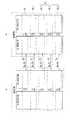
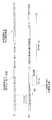
図1は、例えばC−PHY規格やD−PHY規格の通信インタフェースに対応した通信システムの概要を示している。図1に示した通信システムは、送信部TXと、受信部RXとを備えている。また、この通信システムは、送信部TXと受信部RXとに跨がって、クロック信号を伝送するクロックレーンCLと、例えば画像データ等のデータ信号を伝送するデータレーンDLとを備えている。なお、図1では、データレーンDLとして、4つのデータレーンDL1,DL2,DL3,DL4を有した例を示しているが、データレーンDLの数はこれに限らず、例えば1つのデータレーンDL1のみであってもよい。 FIG. 1 shows an outline of a communication system corresponding to, for example, a C-PHY standard or a D-PHY standard communication interface. The communication system shown in FIG. 1 includes a transmission unit TX and a reception unit RX. Further, this communication system includes a clock lane CL that transmits a clock signal across a transmission unit TX and a reception unit RX, and a data lane DL that transmits a data signal such as image data. Note that FIG. 1 shows an example in which four data lanes DL1, DL2, DL3, and DL4 are provided as the data lane DL, but the number of data lane DLs is not limited to this, for example, only one data lane DL1. It may be.
送信部TXは、送信デジタル回路TX−DIGITALと、送信アナログ回路TX−ANALOGとを有している。送信デジタル回路TX−DIGITALと送信アナログ回路TX−ANALOGとの間では、例えば16ビットや8ビットのパラレル信号が伝送される。 The transmission unit TX includes a transmission digital circuit TX-DIGITAL and a transmission analog circuit TX-ANALOG. For example, a 16-bit or 8-bit parallel signal is transmitted between the transmission digital circuit TX-DIGITAL and the transmission analog circuit TX-ANALOG.
受信部RXは、受信デジタル回路RX−DIGITALと、受信アナログ回路RX−ANALOGとを有している。データレーンDL1,DL2,DL3,DL4において、受信アナログ回路RX−ANALOGと受信デジタル回路RX−DIGITALとの間では、例えば16ビットや8ビットのパラレル信号が伝送される。クロックレーンCLにおいて、受信アナログ回路RX−ANALOGと受信デジタル回路RX−DIGITALとの間では、例えば2ビットのシリアル信号が伝送される。 The receiving unit RX has a receiving digital circuit RX-DIGITAL and a receiving analog circuit RX-ANALOG. In the data lanes DL1, DL2, DL3, DL4, for example, a 16-bit or 8-bit parallel signal is transmitted between the reception analog circuit RX-ANALOG and the reception digital circuit RX-DIGITAL. In the clock lane CL, for example, a 2-bit serial signal is transmitted between the reception analog circuit RX-ANALOG and the reception digital circuit RX-DIGITAL.
クロックレーンCLにおいて、送信アナログ回路TX−ANALOGと受信アナログ回路RX−ANALOGとの間は、差動のクロック信号を伝送するクロック信号線30で接続されている。データレーンDL1,DL2,DL3,DL4において、送信アナログ回路TX−ANALOGと受信アナログ回路RX−ANALOGとの間は、差動のデータ信号を伝送するデータ信号線31,32,33,34で接続されている。クロック信号線30とデータ信号線31,32,33,34とはそれぞれ、差動信号を伝送する一対のポジティブ信号線Dpとネガティブ信号線Dnとを有している。クロック信号線30とデータ信号線31,32,33,34とにはそれぞれ、例えば2ビットのシリアル信号が伝送される。 In the clock lane CL, the transmission analog circuit TX-ANALOG and the reception analog circuit RX-ANALOG are connected by a
図2は、図1に示した通信システムを実現する、比較例に係る通信システムの一構成例を示している。なお、図2では、図1におけるデータレーンDLとして、1つのデータレーンDL1のみを示すが、他のデータレーンDL2,DL3,DL4についても略同様の構成であってもよい、 FIG. 2 shows a configuration example of a communication system according to a comparative example that realizes the communication system shown in FIG. In FIG. 2, only one data lane DL1 is shown as the data lane DL in FIG. 1, but the other data lanes DL2, DL3, and DL4 may have substantially the same configuration.
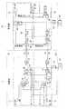
この比較例に係る通信システムは、図1の送信部TXに相当する送信部101と、図1の受信部RXに相当する受信部102とを備えている。 The communication system according to this comparative example includes a
クロックレーンCLにおいて、送信部101は、HS差動信号の処理を行うCL−HS回路111と、LP信号の処理を行うCL−LP回路112とを有している。データレーンDL1において、送信部101は、HS差動信号の処理を行うDL−HS回路113と、LP信号の処理を行うDL−LP回路114とを有している。 In the clock lane CL, the
クロックレーンCLにおいて、受信部102は、HS差動信号の処理を行うCL−HS回路121と、LP信号の処理を行うCL−LP回路122とを有している。データレーンDL1において、受信部102は、HS差動信号の処理を行うDL−HS回路123と、LP信号の処理を行うDL−LP回路124とを有している。 In the clock lane CL, the receiving
図3は、図2に示した比較例に係る通信システムの具体的な回路構成例を示している。また、図4は、図2に示した比較例に係る通信システムにおいてクロックレーンCLとデータレーンDL1とに伝送されるそれぞれの信号波形の一例を示している。 FIG. 3 shows a specific circuit configuration example of the communication system according to the comparative example shown in FIG. Further, FIG. 4 shows an example of each signal waveform transmitted to the clock lane CL and the data lane DL1 in the communication system according to the comparative example shown in FIG.
図4に示したように、この比較例に係る通信システムでは、クロックレーンCLにおいて、送信部101からクロック信号線30に出力される信号のステータスは、HS差動信号で伝送する状態となるHPS(High Speed State)の期間と、LP信号で伝送する状態となるLPS(Low Power State)の期間とが存在する。実質的なクロック信号は、HPSの期間にHS差動信号で出力される。 As shown in FIG. 4, in the communication system according to this comparative example, in the clock lane CL, the status of the signal output from the
同様に、データレーンDL1において、送信部101からデータ信号線31に出力される信号のステータスは、HS差動信号で伝送する状態となるHPSの期間と、LP信号で伝送する状態となるLPSの期間とが存在する。実質的なデータ信号は、HPSの期間にHS差動信号で出力される。なお、図4において、実質的なデータ信号の部分をHSTと記す。また、HPSの期間には、TRAIL期間THS-TRAILやSYNC(同期)期間THS-SYNC等が含まれる。実質的なデータ信号の部分を含まないブランキング期間は、LPSの期間に含まれる。実質的なデータ信号は、例えばByte単位で出力される。Similarly, in the data lane DL1, the status of the signal output from the
図3に示したように、この通信システムは、送信部101内の各回路部にクロック信号を供給する水晶発振器(XTAL)82およびPLL回路81と、受信部102内の各回路部にクロック信号を供給する水晶発振器(XTAL)83とを有している。 As shown in FIG. 3, this communication system has a crystal oscillator (XTAL) 82 and a
CL−HS回路111は、HSステートマシン(HS FSM)51と、セレクタ52と、パラレル/シリアル(PS)変換回路53と、クロック分周器(DIV)54と、HSドライバ(HS DRV)55とを有している。セレクタ52は、Toggle信号と、値0の信号(ALL0)と、値1の信号(ALL1)とを選択的に出力する。Toggle信号は、例えば8ビットのクロック信号(1010_1010)である。 The CL-
CL−LP回路112は、LPステートマシン(LP FSM)41と、LPエンコーダ(LP ENC)42と、LPドライバ(LP DRV)43とを有している。LPステートマシン41には、クロックレーン制御信号が入力される。 The CL-
DL−HS回路113は、HSステートマシン(HS FSM)71と、セレクタ72と、パラレル/シリアル(PS)変換回路73と、HSドライバ(HS DRV)74とを有している。HSステートマシン71からは、データ送信準備完了信号TxReadyHSが出力される。セレクタ72は、送信データTxDataHSと、同期コード信号SYNCと、値0の信号(ALL0)と、値1の信号(ALL1)とを選択的に出力する。 The DL-
DL−LP回路114は、LPステートマシン(LP FSM)61と、LPエンコーダ(LP ENC)62と、LPドライバ(LP DRV)63とを有している。LPステートマシン61には、データ送信要求信号TxRequestHSが入力される。 The DL-
なお、送信部101において、LPドライバ43と、HSドライバ55と、LPドライバ63と、HSドライバ74は、図1における送信アナログ回路TX−ANALOGに相当する。 In the
CL−HS回路121は、クロック信号終端回路としての終端回路(TERM)56と、HSレシーバ(HS RCV)57と、クロック分周器(DIV)58とを有している。終端回路56は、終端抵抗を有している。 The CL-
CL−LP回路122は、LPレシーバ(LP RCV)44と、LPデコーダ(LP DEC)45と、LPステートマシン(LP FSM)46とを有している。LPステートマシン46は、クロックレーンCLのステータス信号を出力する。 The CL-
DL−HS回路123は、データ信号終端回路としての終端回路(TERM)75と、HSレシーバ(HS RCV)76と、クロック分周器(DIV)77と、ワードアライン補正回路(ALN)78とを有している。終端回路75は、終端抵抗を有している。ワードアライン補正回路(ALN)78は、受信同期信号RxSyncHSと、受信有効信号RxValidHSと、受信データRxDataHSとを出力する。 The DL-
DL−LP回路124は、LPレシーバ(LP RCV)64、LPデコーダ(LP DEC)65、LPステートマシン(LP FSM)66とを有している。LPステートマシン66は、受信アクティブ信号RxActiveHSを出力する。 The DL-
なお、受信部102において、主として、LPレシーバ44と、終端回路56と、HSレシーバ57と、LPレシーバ64と、終端回路75と、HSレシーバ76とが、図1における受信アナログ回路RX−ANALOGに相当する。 In the receiving
<1.第1の実施の形態>
次に、本開示の第1の実施の形態について説明する。以下では、上記比較例と略同様の構成および作用を有する部分については、適宜説明を省略する。<1. First Embodiment>
Next, the first embodiment of the present disclosure will be described. In the following, the description of the portion having substantially the same configuration and operation as the above comparative example will be omitted as appropriate.
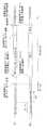
図5は、図1に示した通信システムを実現する、本開示の第1の実施の形態に係る通信システムの概要を示している。図6は、図5に示した通信システムの具体的な回路構成例を示している。また、図7は、図5に示した通信システムにおいてクロックレーンCLとデータレーンDL1とに伝送されるそれぞれの信号波形の一例を示している。なお、図5ないし図7では、図1におけるデータレーンDLとして、1つのデータレーンDL1のみを示すが、他のデータレーンDL2,DL3,DL4についても略同様の構成であってもよい。 FIG. 5 shows an outline of the communication system according to the first embodiment of the present disclosure, which realizes the communication system shown in FIG. FIG. 6 shows a specific circuit configuration example of the communication system shown in FIG. Further, FIG. 7 shows an example of each signal waveform transmitted to the clock lane CL and the data lane DL1 in the communication system shown in FIG. Although only one data lane DL1 is shown as the data lane DL in FIGS. 5 to 7, the other data lanes DL2, DL3, and DL4 may have substantially the same configuration.
本実施の形態に係る通信システムは、図1の送信部TXに相当する送信部1(送信装置)と、図1の受信部RXに相当する受信部2(受信装置)とを備えている。 The communication system according to the present embodiment includes a transmitting unit 1 (transmitting device) corresponding to the transmitting unit TX of FIG. 1 and a receiving unit 2 (receiving device) corresponding to the receiving unit RX of FIG.
図7に示したように、本実施の形態に係る通信システムでは、クロックレーンCLにおいて、送信部1からクロック信号線30に出力される信号は、ブランキング期間も含めてすべてHS差動信号のみとなっている。後述するように、クロックレーンCLにおいて、ブランキング期間には、送信部1からクロック信号線30に、所定のブランキング信号として、所定の第1の信号値(例えばHS−0)の差動ブランキング信号と、所定の第1の信号値とは異なる所定の第2の信号値(例えばHS−1)の差動信号とが出力される。 As shown in FIG. 7, in the communication system according to the present embodiment, in the clock lane CL, all the signals output from the
なお、HS−0は値0(差動0(Differential-0))となる差動信号、HS−1は値1(差動1(Differential-1))となる差動信号を示す。より具体的には、図8に示したように、HS−0の信号は、差動信号の伝送線におけるポジティブ信号線Dpの電圧レベルがLowとなり、ネガティブ信号線Dnの電圧レベルがHighとなる差動信号のことを言う。また、HS−1の信号は、差動信号の伝送線におけるポジティブ信号線Dpの電圧レベルがHighとなり、ネガティブ信号線Dnの電圧レベルがLowとなる差動信号のことを言う。 HS-0 indicates a differential signal having a value of 0 (differential 0 (Differential-0)), and HS-1 indicates a differential signal having a value of 1 (differential 1 (Differential-1)). More specifically, as shown in FIG. 8, in the HS-0 signal, the voltage level of the positive signal line Dp in the transmission line of the differential signal is Low, and the voltage level of the negative signal line Dn is High. It refers to a differential signal. Further, the HS-1 signal is a differential signal in which the voltage level of the positive signal line Dp in the transmission line of the differential signal is High and the voltage level of the negative signal line Dn is Low.
同様に、データレーンDL1において、送信部1からデータ信号線31に出力される信号は、ブランキング期間も含めてすべてHS差動信号のみとなっている。
なお、図7において、実質的なデータ信号の部分をHSTと記す。実質的なデータ信号の前後の期間にはSYNC(同期)期間THS-SYNCとTRAIL期間THS-TRAILとが含まれていてもよい。データレーンDL1において、ブランキング期間には、送信部1からデータ信号線31に、所定のデータブランキング信号として、任意の差動信号(例えばHS−0またはHS−1)をブランキング期間の全体に亘って出力してもよい。Similarly, in the data lane DL1, all the signals output from the
In FIG. 7, the portion of the substantial data signal is referred to as HST. The period before and after the substantial data signal may include a SYNC (synchronous) period THS-SYNC and a TRAIL period THS-TRAIL . In the data lane DL1, during the blanking period, an arbitrary differential signal (for example, HS-0 or HS-1) is transmitted from the
図6に示したように、本実施の形態に係る通信システムは、送信部1内の各回路部にクロック信号を供給する水晶発振器(XTAL)82およびPLL回路81と、受信部2内の各回路部にクロック信号を供給する水晶発振器(XTAL)83およびPLL回路84とを有している。 As shown in FIG. 6, the communication system according to the present embodiment includes a crystal oscillator (XTAL) 82 and a
クロックレーンCLにおいて、送信部1は、HS差動信号の処理を行うCL−HS回路11を有している。データレーンDL1において、送信部1は、HS差動信号の処理を行うDL−HS回路13を有している。
CL−HS回路11は、差動のクロック信号を含むHS差動信号をクロック信号線30に出力する差動クロック信号送信回路であってもよい。DL−HS回路13は、差動のデータ信号をデータ信号線31に出力する差動データ信号送信回路であってもよい。In the clock lane CL, the
The CL-
本実施の形態における送信部1には、上記比較例におけるLP信号の処理を行うCL−LP回路112およびDL−LP回路114に相当する回路は含まれていなくともよい。 The
CL−HS回路11は、図6に示したように、図3におけるCL−HS回路111と略同様の回路を有していてもよい。すなわち、CL−HS回路11は、HSステートマシン(HS FSM)51と、セレクタ52と、パラレル/シリアル(PS)変換回路53と、クロック分周器(DIV)54と、HSドライバ(HS DRV)55とを有していてもよい。セレクタ52は、Toggle信号と、所定の第1の信号値(HS−0)となる値0の信号(ALL0)と、所定の第2の信号値(HS−1)となる値1の信号(ALL1)とを選択的に出力する。Toggle信号は、例えば8ビットのクロック信号(1010_1010)である。本実施の形態では、クロックレーン制御信号とデータ送信要求信号TxRequestHSとが、HSステートマシン51に入力される。 As shown in FIG. 6, the CL-
DL−HS回路13は、図6に示したように、図3におけるDL−HS回路113と略同様の回路を有していてもよい。すなわち、DL−HS回路13は、HSステートマシン(HS FSM)71と、セレクタ72と、パラレル/シリアル(PS)変換回路73と、HSドライバ(HS DRV)74とを有していてもよい。HSステートマシン71からは、データ送信準備完了信号TxReadyHSが出力される。セレクタ72は、送信データTxDataHSと、同期コード信号SYNCと、所定の第1の信号値(HS−0)となる値0の信号(ALL0)と、所定の第2の信号値(HS−1)となる値1の信号(ALL1)とを選択的に出力する。 As shown in FIG. 6, the DL-
送信部1は、ブランキング制御部20を有している。図6に示したように、ブランキング制御部20は、HSステートマシン51とHSステートマシン71とを有していてもよい。 The
ブランキング制御部20は、データ信号のブランキング期間の開始時刻に同期して、DL−HS回路13からデータ信号線31に、データ信号に代えて、所定のデータブランキング信号が出力されるよう、DL−HS回路13を制御する。また、ブランキング制御部20は、データ信号のブランキング期間の開始時刻に同期して、CL−HS回路11からクロック信号線30に、クロック信号に代えて所定の期間以上に亘って所定の第1の信号値(例えばHS−0)が連続する差動ブランキング信号が出力されるよう、CL−HS回路11を制御する。ここで、所定の期間とは、クロック信号のクロック周期よりも長い期間である。差動ブランキング信号を、クロック信号のクロック周期よりも長い期間に亘って所定の第1の信号値が連続する信号とすることで、後述する受信部2のクロック状態判別回路59において、信号の変化を検出することができ、ブランキング期間が開始されたことを検出することが可能となる。 The blanking
また、ブランキング制御部20は、データ信号のブランキング期間の終了時刻に同期して、CL−HS回路11からクロック信号線30に、差動ブランキング信号に代えて、差動ブランキング信号とは異なる所定の差動信号が出力されるよう、CL−HS回路11を制御する。具体的には、所定の差動信号として、所定の第1の信号値とは異なる所定の第2の信号値(例えばHS−1)が所定の期間以上に亘って連続する差動の信号が出力されるよう、CL−HS回路11を制御する。なお、以上の説明における所定の第1の信号値をHS−1、所定の第2の信号値をHS−0にしてもよい。所定の差動信号を、所定の第1の信号値とは異なる所定の第2の信号値が所定の期間以上に亘って連続する差動の信号とすることで、後述する受信部2のクロック状態判別回路59において、信号の変化を検出することができ、ブランキング期間が終了し、データ信号の転送が開始されることを検出することが可能となる。 Further, the blanking
クロックレーンCLにおいて、受信部2は、HS差動信号の処理を行うCL−HS回路21を有している。データレーンDL1において、受信部2は、HS差動信号の処理を行うDL−HS回路23を有している。 In the clock lane CL, the receiving
DL−HS回路23は、差動のデータ信号をデータ信号線31を介して受信する差動データ信号受信回路であってもよい。CL−HS回路21は、差動のクロック信号と、上記したCL−HS回路11から出力された差動ブランキング信号とを、クロック信号線30を介して受信する差動クロック信号受信回路であってもよい。 The DL-
本実施の形態における受信部2には、上記比較例におけるLP信号の処理を行うCL−LP回路122およびDL−LP回路124に相当する回路は含まれていなくともよい。 The receiving
DL−HS回路23は、図6に示したように、図3におけるDL−HS回路123と略同様の回路を有していてもよい。すなわち、データ信号線31に接続されたデータ信号終端回路としての終端回路(TERM)75と、HSレシーバ(HS RCV)76と、クロック分周器(DIV)77と、ワードアライン補正回路(ALN)78とを有していてもよい。終端回路75は、終端抵抗を有している。ワードアライン補正回路(ALN)78は、受信同期信号RxSyncHSと、受信有効信号RxValidHSと、受信データRxDataHSとを出力する。 As shown in FIG. 6, the DL-
CL−HS回路21は、図6に示したように、図3におけるCL−HS回路121と略同様の回路を有していてもよい。すなわち、CL−HS回路21は、クロック信号線30に接続されたクロック信号終端回路としての終端回路(TERM)56と、HSレシーバ(HS RCV)57と、クロック分周器(DIV)58とを有していてもよい。終端回路56は、終端抵抗を有している。 As shown in FIG. 6, the CL-
CL−HS回路21は、さらに、クロック(CL)状態判別回路59を有している。クロック状態判別回路59には、HSレシーバ57を介して送信部1のCL−HS回路11からのクロック信号と、所定の第1の信号値(例えばHS−0)の差動ブランキング信号(例えばHS−0)と、所定の第2の信号値(例えばHS−1)の差動信号とが入力される。 The CL-
クロック状態判別回路59は、終端制御回路としての機能を有し、差動ブランキング信号に基づいて、データ信号終端回路(終端回路75)およびクロック信号終端回路(終端回路56)に対してそれぞれの終端抵抗をオフさせる制御を行う。また、クロック状態判別回路59は、データ信号のブランキング期間の終了時刻に同期して出力された、所定の第2の信号値(例えばHS−1)の差動信号に基づいて、終端回路75および終端回路56に対してそれぞれの終端抵抗をオンさせる制御を行う。 The clock
なお、終端抵抗のオン/オフに伴い、図7に示したように、クロックレーンCLおよびデータレーンDL1のブランキング期間における信号の電圧振幅が変化する。また、ブランキング期間において終端抵抗をオフさせることにより、クロック信号線30およびデータ信号線31に流れる電流値を低減することができる。
As shown in FIG. 7, the voltage amplitude of the signal in the blanking period of the clock lane CL and the data lane DL1 changes as the terminating resistor is turned on / off. Further, by turning off the terminatingresistor during the blanking period, the current value flowing through the
また、クロック状態判別回路59は、受信アクティブ信号RxActiveHSを出力しワードアライン補正回路78に対して、ワードアライン制御を行う機能を有している。ブランキング期間が終了し、データ信号の転送が開始されることをクロック状態判別回路59において適切に検出することで、同期コード信号SYNCを検出し、ワードアライン補正回路78で適切にワードアライン制御を行うことができる。 Further, the clock
[効果]
以上のように、本実施の形態によれば、データ信号のブランキング期間の開始時刻に同期して、クロック信号線30に、クロック信号に代えて所定の期間以上に亘って所定の第1の信号値が連続する差動ブランキング信号を出力するようにしたので、データ伝送時の低消費電力化を図ることができる。[effect]
As described above, according to the present embodiment, in synchronization with the start time of the blanking period of the data signal, the
また、クロック信号線30を介して、差動のクロック信号と、データ信号のブランキング期間の開始時刻に同期して所定の期間以上に亘って所定の第1の信号値が連続するように出力された差動ブランキング信号とを受信するようにしたので、データ伝送時の低消費電力化を図ることができる。 Further, the differential clock signal and the predetermined first signal value are continuously output for a predetermined period or longer in synchronization with the start time of the blanking period of the data signal via the
また、本実施の形態によれば、上記した比較列に係る通信システムでは有効に活用されていなかったLP信号部分(ブランキング期間)にもHS差動信号によるデータ信号を転送することが可能となり、HS差動信号によるデータ信号の転送レートを下げ、全体として低消費電力化を実現することができる。また、本実施の形態によれば、上記した比較列に係る通信システムと比べて、LP信号の処理を行う回路が不要となり、回路規模を削減することができる。 Further, according to the present embodiment, it is possible to transfer the data signal by the HS differential signal to the LP signal portion (blanking period) which has not been effectively utilized in the communication system related to the comparison column described above. , The transfer rate of the data signal by the HS differential signal can be lowered, and the power consumption can be reduced as a whole. Further, according to the present embodiment, as compared with the communication system related to the comparison column described above, a circuit for processing the LP signal becomes unnecessary, and the circuit scale can be reduced.
なお、本明細書に記載された効果はあくまでも例示であって限定されるものではなく、また他の効果があってもよい。以降の他の実施の形態の効果についても同様である。 It should be noted that the effects described in the present specification are merely examples and are not limited, and other effects may be obtained. The same applies to the effects of the other embodiments thereafter.
<2.第2の実施の形態>
次に、本開示の第2の実施の形態について説明する。以下では、上記比較例、上記第1の実施の形態と略同様の構成および作用を有する部分については、適宜説明を省略する。<2. Second Embodiment>
Next, a second embodiment of the present disclosure will be described. In the following, description of the comparative example and the portion having substantially the same configuration and operation as that of the first embodiment will be omitted as appropriate.
図9は、本実施の形態に係る通信システムの具体的な回路構成例を示している。また、図10は、本実施の形態に係る通信システムにおいてクロックレーンCLとデータレーンDL1とに伝送されるそれぞれの信号波形の一例を示している。なお、図9および図10では、図1におけるデータレーンDLとして、1つのデータレーンDL1のみを示すが、他のデータレーンDL2,DL3,DL4についても略同様の構成であってもよい。なお、本実施の形態に係る通信システムの概要を示すブロック構成は、図5と略同様であってもよい。 FIG. 9 shows a specific circuit configuration example of the communication system according to the present embodiment. Further, FIG. 10 shows an example of each signal waveform transmitted to the clock lane CL and the data lane DL1 in the communication system according to the present embodiment. Note that, in FIGS. 9 and 10, only one data lane DL1 is shown as the data lane DL in FIG. 1, but the other data lanes DL2, DL3, and DL4 may have substantially the same configuration. The block configuration showing the outline of the communication system according to the present embodiment may be substantially the same as that in FIG.
本実施の形態においても、上記第1の実施の形態と同様に、ブランキング制御部20が、データ信号のブランキング期間の終了時刻に同期して、CL−HS回路11からクロック信号線30に、差動ブランキング信号に代えて、差動ブランキング信号とは異なる所定の差動信号が出力されるよう、CL−HS回路11を制御する。上記第1の実施の形態では、所定の差動信号として、所定の第2の信号値(例えばHS−1)が所定の期間以上に亘って連続する差動の信号が出力されるよう、CL−HS回路11を制御する。これに対して、本実施の形態では、所定の差動信号として、所定の期間以上に亘ってクロック信号が出力されるよう、CL−HS回路11を制御する。所定の差動信号を、所定の期間以上に亘るクロック信号とすることで、受信部2Aのクロック状態判別回路59において、信号の変化を検出することができ、ブランキング期間が終了し、データ信号の転送が開始されることを検出することが可能となる。 Also in the present embodiment, similarly to the first embodiment, the blanking
本実施の形態では、図7に示したように、クロックレーンCLにおいて、ブランキング期間には、送信部1からクロック信号線30に、所定の第1の信号値(例えばHS−0またはHS−1)の差動ブランキング信号と、クロック信号とが出力される。 In the present embodiment, as shown in FIG. 7, in the clock lane CL, during the blanking period, a predetermined first signal value (for example, HS-0 or HS-) is transmitted from the
図6の回路構成と比較して、図9の回路では、受信部2AのCL−HS回路21におけるクロック状態判別回路59に入力される信号が異なっている。すなわち、図6の回路構成の受信部2では、クロック状態判別回路59には、HSレシーバ57からの信号が直接入力される。これに対して、図9の回路構成の受信部2Aでは、クロック状態判別回路59には、HSレシーバ57からの信号は直接入力されず、クロック分周器58で分周された信号が入力される。これにより、ブランキング期間の開始時刻および終了時刻を検出する。 Compared with the circuit configuration of FIG. 6, in the circuit of FIG. 9, the signal input to the clock
その他の構成および動作は、上記第1の実施の形態に係る通信システムと略同様であってもよい。 Other configurations and operations may be substantially the same as those of the communication system according to the first embodiment.
[2.2 変形例]
次に、第2の実施の形態の通信システムの第1ないし第5の変形例にっいて説明する。[2.2 Modification example]
Next, the first to fifth modifications of the communication system of the second embodiment will be described.
図11〜図15は、第1ないし第5の変形例に係る通信システムにおいてクロックレーンCLとデータレーンDL1とに伝送されるそれぞれの信号波形の一例を示している。なお、図11〜図15では、図1におけるデータレーンDLとして、1つのデータレーンDL1のみを示すが、他のデータレーンDL2,DL3,DL4についても略同様であってもよい。また、本実施の形態に係る通信システムの概要を示すブロック構成は、図5と略同様であってもよい。 11 to 15 show an example of each signal waveform transmitted to the clock lane CL and the data lane DL1 in the communication system according to the first to fifth modifications. Note that, in FIGS. 11 to 15, only one data lane DL1 is shown as the data lane DL in FIG. 1, but the same may be applied to the other data lanes DL2, DL3, and DL4. Further, the block configuration showing the outline of the communication system according to the present embodiment may be substantially the same as that in FIG.
(第1の変形例)
図11に示した第1の変形例では、図10に示した例に対して、ブランキング期間に送信部1からデータレーンDL1に出力される信号が異なっている。データレーンDL1において、ブランキング期間には、送信部1のDL−HS回路13から、まず、所定のデータブランキング信号として、HSTの期間に伝送される実質的なデータ信号の最後の値の反転値の差動信号が出力される。その後、DL−HS回路13から、差動0(HS−0)の差動信号が出力される。(First modification)
In the first modification shown in FIG. 11, the signal output from the
ブランキング制御部20は、ブランキング期間の開始時刻に同期して、DL−HS回路13からデータ信号線31に、データ信号の最後の値の反転値の差動信号が出力されるよう、DL−HS回路13を制御する。また、ブランキング制御部20は、ブランキング期間の終了時刻に同期して、データ信号の最後の値の反転値の差動信号に代えて、DL−HS回路13からデータ信号線31に、HS−0の差動信号が出力されるよう、DL−HS回路13を制御する。なお、クロック信号線30には、図10の例と同様に、ブランキング期間の終了時刻に同期して、送信部1のCL−HS回路11からクロック信号線30に所定の期間以上に亘ってクロック信号が出力される。ブランキング期間に出力されるHS−0の差動信号とクロック信号とのそれぞれの出力の開始時刻は、異なっていてもよい。 The blanking
この第1の変形例によれば、データレーンDL1におけるブランキング期間の最後の期間をHS−0の差動信号にすることで、ブランキング期間の最後の期間の信号値と、次に続くSYNC(同期)期間THS-SYNCの開始時の信号値とが同じ値になり、受信側の同期の処理を容易にすることができる。また、一般に、データレーンDL1におけるTRAIL期間THS-TRAILの信号は、データ信号の最後の値の反転値の差動信号となっている。このため、この第1の変形例によれば、ブランキング期間の開始時の信号値をTRAIL期間THS-TRAILの信号に合わせることができる。According to this first modification, by making the last period of the blanking period in the data lane DL1 a differential signal of HS-0, the signal value of the last period of the blanking period and the following SYNC (Synchronization) The signal value at the start of theHS-SYNC period becomes the same value, and the synchronization process on the receiving side can be facilitated. Further, in general, the signal of the TRAIL periodTHS-TRAIL in the data lane DL1 is a differential signal of the inverted value of the last value of the data signal. Therefore, according to this first modification, the signal value at the start of the blanking period can be matched with the signal of the TRAIL periodTHS-TRAIL .
その他は、図10の信号波形と略同様であってもよい。 Others may be substantially the same as the signal waveform of FIG.
(第2の変形例)
図12に示した第2の変形例では、図11に示した第1の変形例に対して、送信部1のCL−HS回路11からクロック信号線30に出力される信号が一部異なっている。クロックレーンCLにおいて、ブランキング期間には、送信部1のCL−HS回路11から、まず、図7に示した上記第1の実施の形態と同様に、所定の第1の信号値(例えばHS−0またはHS−1)の差動信号が出力される。その後、上記第1の実施の形態と同様に、CL−HS回路11から、所定の第1の信号値とは異なる所定の第2の信号値(例えばHS−1またはHS−0)の差動信号が出力される。その後、終端抵抗をオンさせる時刻を経過した後、CL−HS回路11からクロック信号が出力される。CL−HS回路11から、所定の第2の信号値の差動信号を出力した後、終端抵抗をオンさせる時刻を挟んで、次に、クロック信号を出力する点が、上記第1の実施の形態とは異なっている。ブランキング制御部20は、CL−HS回路11から適切なタイミングで差動信号とクロック信号とが出力されるよう、CL−HS回路11を制御する。
(Second modification)
In the second modification shown in FIG. 12, the signal output from the CL-
この第2の変形例によれば、第1の変形例のようにクロック信号の出力期間中に終端抵抗をオンさせる場合に比べて、クロックレーンCLにおける終端抵抗オフ時のクロック信号の反射による波形の乱れの影響を低減することができる。 According to this second modification, the waveform due to the reflection of the clock signal when the terminating resistor is off in the clock lane CL is compared with the case where the terminating resistor is turned on during the output period of the clock signal as in the first modification. The influence of the disturbance can be reduced.
その他は、図11の第1の変形例と略同様であってもよい。 Others may be substantially the same as the first modification of FIG.
(第3の変形例)
図13に示した第3の変形例では、図12に示した第2の変形例に対して、ブランキング期間に送信部1からデータレーンDL1に出力される信号が異なっている。この第3の変形例では、ブランキング期間全体に亘って、送信部1のDL−HS回路13から、所定のデータブランキング信号として、HS−0の差動信号が出力される。ブランキング制御部20は、DL−HS回路13から適切なタイミングでHS−0の差動信号が出力されるよう、DL−HS回路13を制御する。(Third variant)
In the third modification shown in FIG. 13, the signal output from the
その他は、図12の第2の変形例と略同様であってもよい。 Others may be substantially the same as the second modification of FIG.
(第4の変形例)
図14に示した第4の変形例では、図11に示した第1の変形例に対して、ブランキング期間に送信部1からデータレーンDL1に出力される信号が一部異なっている。この第4の変形例では、データレーンDL1において、ブランキング期間には、送信部1のDL−HS回路13から、まず、所定のデータブランキング信号として、HS−1の差動信号が出力される。その後、DL−HS回路13から、HS−0の差動信号が出力される。ブランキング制御部20は、DL−HS回路13から適切なタイミングでHS−1の差動信号とHS−0の差動信号とが出力されるよう、DL−HS回路13を制御する。(Fourth modification)
In the fourth modification shown in FIG. 14, the signal output from the
その他は、図11の第1の変形例と略同様であってもよい。 Others may be substantially the same as the first modification of FIG.
(第5の変形例)
図15に示した第5の変形例では、図12に示した第2の変形例に対して、ブランキング期間に送信部1からデータレーンDL1に出力される信号が一部異なっている。この第5の変形例では、データレーンDL1において、ブランキング期間には、送信部1のDL−HS回路13から、まず、所定のデータブランキング信号として、HS−1の差動信号が出力される。その後、DL−HS回路13から、HS−0の差動信号が出力される。ブランキング制御部20は、DL−HS回路13から適切なタイミングでHS−1の差動信号とHS−0の差動信号とが出力されるよう、DL−HS回路13を制御する。(Fifth variant)
In the fifth modification shown in FIG. 15, the signal output from the
その他は、図12の第2の変形例と略同様であってもよい。 Others may be substantially the same as the second modification of FIG.
<3.第3の実施の形態>
次に、本開示の第3の実施の形態について説明する。以下では、上記比較例、上記第1の実施の形態または上記第2の実施の形態と略同様の構成および作用を有する部分については、適宜説明を省略する。<3. Third Embodiment>
Next, a third embodiment of the present disclosure will be described. In the following, description of the comparative example, the first embodiment, or the portion having substantially the same configuration and operation as that of the second embodiment will be omitted as appropriate.
図16は、本開示の第3の実施の形態に係る通信システムの概要を示している。本実施の形態に係る通信システムは、図1の送信部TXに相当する送信部1B(送信装置)と、図1の受信部RXに相当する受信部2B(受信装置)とを備えている。 FIG. 16 shows an outline of the communication system according to the third embodiment of the present disclosure. The communication system according to the present embodiment includes a transmitting
上記第1および第2の実施の形態に係る通信システムでは、クロックレーンCLとデータレーンDL1とのそれぞれにおいて伝送される信号を、ブランキング期間も含めてすべてHS差動信号のみにしている。これに対して、本実施の形態に係る通信システムは、LP信号での通信も可能にする切り替え回路を備え、LP信号を用いずにHS差動信号のみで通信を行うモードと、LP信号とHS差動信号との双方を用いて通信を行うモードとを切り替え可能にしたものである。 In the communication system according to the first and second embodiments, the signals transmitted in each of the clock lane CL and the data lane DL1 are all HS differential signals including the blanking period. On the other hand, the communication system according to the present embodiment includes a switching circuit that enables communication with LP signals, and has a mode in which communication is performed only with HS differential signals without using LP signals, and LP signals. It is possible to switch between the mode in which communication is performed using both the HS differential signal and the HS differential signal.
本実施の形態に係る通信システムにおいて、送信部1Bは、上記第1および第2の実施の形態に係る通信システムと略同様の機能を実現するブランキング制御部20を有している。 In the communication system according to the present embodiment, the
また、送信部1Bは、クロックレーンCLにおいて、HS差動信号の処理を行うCL−HS回路11と、LP信号の処理を行うCL−LP回路12と、切り替えスイッチ15と、セレクタ17とを有している。 Further, the
CL−LP回路12は、LP信号として第1のシングルエンド信号を出力する第1のシングルエンド信号送信回路であってもよい。CL−LP回路12は、図2におけるCL−LP回路112と略同様の機能を有するものであってもよい。切り替えスイッチ15は、クロック信号線30に、CL−HS回路11とCL−LP回路12とのいずれか一方から信号出力がなされるよう、信号出力の経路を切り替える第1の送信切り替え回路であってもよい。セレクタ17は、LP信号を用いずにHS差動信号のみで通信を行うモードではブランキング制御部20からの制御信号がCL−HS回路11に入力されるようにし、LP信号とHS差動信号との双方を用いて通信を行うモードでは、ブランキング制御部20からの制御信号がCL−HS回路11に入力されないようにする回路である。 The CL-
また、送信部1Bは、データレーンDL1において、HS差動信号の処理を行うDL−HS回路13と、LP信号の処理を行うDL−LP回路14と、切り替えスイッチ16と、セレクタ18とを有している。 Further, the
DL−LP回路14は、LP信号として第2のシングルエンド信号を出力する第2のシングルエンド信号送信回路であってもよい。DL−LP回路14は、図2におけるDL−LP回路114と略同様の機能を有するものであってもよい。切り替えスイッチ16は、データ信号線31にDL−HS回路13とDL−LP回路14とのいずれか一方から信号出力がなされるよう、信号出力の経路を切り替える第2の送信切り替え回路であってもよい。セレクタ18は、LP信号を用いずにHS差動信号のみで通信を行うモードではブランキング制御部20からの制御信号がDL−HS回路13に入力されるようにし、LP信号とHS差動信号との双方を用いて通信を行うモードでは、ブランキング制御部20からの制御信号がDL−HS回路13に入力されないようにする回路である。 The DL-
受信部2Bは、クロックレーンCLにおいて、HS差動信号の処理を行うCL−HS回路21と、LP信号の処理を行うCL−LP回路22と、セレクタ25と、セレクタ27と、セレクタ28とを有している。CL−LP回路22は、LP信号として第1のシングルエンド信号をクロック信号線30を介して受信する第1のシングルエンド信号受信回路であってもよい。CL−LP回路22は、図2におけるCL−LP回路122と略同様の機能を有するものであってもよい。 In the clock lane CL, the receiving unit 2B includes a CL-
セレクタ25は、LP信号として第1のシングルエンド信号を受信するか否かを切り替える第1の受信切り替え回路であってもよい。セレクタ25は、LP信号を用いずにHS差動信号のみで通信を行うモードではクロック信号線30を介して受信した信号がCL−LP回路22に入力されないようにし、LP信号とHS差動信号との双方を用いて通信を行うモードでは、クロック信号線30を介して受信した信号がCL−LP回路22に入力されるようにする回路である。セレクタ27は、LP信号を用いずにHS差動信号のみで通信を行うモードではCL−HS回路21からの終端制御の信号がDL−HS回路23に入力されるようにし、LP信号とHS差動信号との双方を用いて通信を行うモードでは、HS回路21からの終端制御の信号が入力されないようにする回路である。セレクタ28は、LP信号を用いずにHS差動信号のみで通信を行うモードではCL−HS回路21からのワードアライン制御の信号がDL−HS回路23に入力されるようにし、LP信号とHS差動信号との双方を用いて通信を行うモードでは、HS回路21からのワードアライン制御の信号が入力されないようにする回路である。 The
また、受信部2Bは、データレーンDL1において、HS差動信号の処理を行うDL−HS回路23と、LP信号の処理を行うDL−LP回路24と、セレクタ26とを有している。DL−LP回路24は、LP信号として第2のシングルエンド信号をデータ信号線31を介して受信する第2のシングルエンド信号受信回路であってもよい。 Further, the receiving unit 2B has a DL-
セレクタ26は、LP信号として第2のシングルエンド信号を受信するか否かを切り替える第2の受信切り替え回路であってもよい。セレクタ26は、LP信号を用いずにHS差動信号のみで通信を行うモードではデータ信号線31を介して受信した信号がDL−LP回路24に入力されないようにし、LP信号とHS差動信号との双方を用いて通信を行うモードでは、データ信号線31を介して受信した信号がDL−LP回路24に入力されるようにする回路である。 The
図17は、本実施の形態に係る通信システムの具体的な適用例を示している。 FIG. 17 shows a specific application example of the communication system according to the present embodiment.
例えば、本実施の形態に係る通信システムは、図17に示したように、イメージセンサISからアプリケーションプロセッサAPへのデータ伝送に適用可能である。送信部1Bは、イメージセンサIS内に設けられる。受信部2Bは、アプリケーションプロセッサAP内に設けられる。イメージセンサISとアプリケーションプロセッサAPとの間は、クロック信号線30とデータ信号線31とによって接続される。クロック信号線30とデータ信号線31とによる信号の伝送は一方向となっている。 For example, the communication system according to the present embodiment can be applied to data transmission from the image sensor IS to the application processor AP, as shown in FIG. The
また、イメージセンサISとアプリケーションプロセッサAPとの間は、双方向の制御バス35によって接続される。制御バス35は、I2C(Inter-Integrated Circuit)インタフェースやその拡張版であるI3Cインタフェースを用いることができる。Further, the image sensor IS and the application processor AP are connected by a
図18は、図17に示したイメージセンサISおよびアプリケーションプロセッサAPを含む機器におけるデータ送信処理の一例を示している。 FIG. 18 shows an example of data transmission processing in the device including the image sensor IS and the application processor AP shown in FIG.
イメージセンサISおよびアプリケーションプロセッサAPを含む機器の電源投入がなされる(ステップS101)と、アプリケーションプロセッサAPが、制御バス35を使用して、イメージセンサISのレジスタ設定を読み込む(ステップS102)。これにより、アプリケーションプロセッサAPは、イメージセンサISがLP信号無しでの通信に対応しているか否かを判断する(ステップS103)。すなわち、LP信号を用いずにHS差動信号のみで通信を行うモードと、LP信号とHS差動信号との双方を用いて通信を行うモードとのいずれのモードに対応しているかを判断する。 When the power of the device including the image sensor IS and the application processor AP is turned on (step S101), the application processor AP reads the register setting of the image sensor IS using the control bus 35 (step S102). As a result, the application processor AP determines whether or not the image sensor IS supports communication without the LP signal (step S103). That is, it is determined which mode corresponds to the mode in which communication is performed using only the HS differential signal without using the LP signal and the mode in which communication is performed using both the LP signal and the HS differential signal. ..
LP信号無しでの通信に対応していると判断した場合(ステップS103;Y)には、アプリケーションプロセッサAPは、制御バス35を使用して、LP信号無しでの通信を有効化する設定をイメージセンサISに送信する(ステップS104)。次に、アプリケーションプロセッサAPは、制御バス35を使用して、イメージセンサISに送信開始指示の信号を出力する(ステップS105)。LP信号無しでの通信に対応していないと判断した場合(ステップS103;N)には、アプリケーションプロセッサAPは、LP信号とHS差動信号との双方を用いて通信を行うモードとみなして、制御バス35を使用して、イメージセンサISに送信開始指示の信号を出力する(ステップS105)。次に、イメージセンサISは、送信開始指示の信号を受けて、データ信号の送信を開始する(ステップS106)。 When it is determined that the communication without the LP signal is supported (step S103; Y), the application processor AP uses the
<4.第4の実施の形態>
次に、本開示の第4の実施の形態について説明する。以下では、上記比較例、または、上記第1ないし第3の実施の形態と略同様の構成および作用を有する部分については、適宜説明を省略する。<4. Fourth Embodiment>
Next, a fourth embodiment of the present disclosure will be described. Hereinafter, the description of the comparative example or the portion having substantially the same configuration and operation as that of the first to third embodiments will be omitted as appropriate.
図19は、本開示の第4の実施の形態に係る通信システムの概要を示している。図20は、本実施の形態に係る通信システムにおいてクロックレーンCLとデータレーンDL1とに伝送されるそれぞれの信号波形の第1の例を示している。図21は、本実施の形態に係る通信システムにおいてクロックレーンCLとデータレーンDL1とに伝送されるそれぞれの信号波形の第2の例を示している。なお、図19ないし図21では、図1におけるデータレーンDLとして、1つのデータレーンDL1のみを示すが、他のデータレーンDL2,DL3,DL4についても略同様の構成であってもよい。
FIG. 19 shows an outline of the communication system according to the fourth embodiment of the present disclosure. FIG. 20 shows a first example of each signal waveform transmitted to the clock lane CL and the data lane DL1 in the communication system according to the present embodiment. FIG. 21 shows a second example of each signal waveform transmitted to the clock lane CL and the data lane DL1 in the communication system according to the present embodiment. In FIG 21Figures 19, the data lanes DL in FIG. 1 shows only one data lane DL1, other data lanes DL2, DL3, DL4 may be substantially similar configuration for.
本実施の形態に係る通信システムは、図5に示した通信システムの構成に対して、終端制御の部分が異なっている。上記第1ないし第3の実施の形態では、ブランキング期間において、終端抵抗のオン/オフの制御を行うようにしたが、本実施の形態では、この終端抵抗のオン/オフの制御を省略している。 The communication system according to the present embodiment is different in the terminal control part from the configuration of the communication system shown in FIG. In the first to third embodiments described above, the on / off control of the terminating resistor is controlled during the blanking period, but in the present embodiment, the on / off control of the terminating resistor is omitted. ing.
図20の第1の例では、クロックレーンCLとデータレーンDL1とにおける終端抵抗を常時、オンの状態にした場合の例を示している。図20の第1の例の場合、オン/オフの切り替え可能な終端抵抗を設け、終端抵抗を常時、オンの状態にしてもよいし、常時、オンとなる固定の終端抵抗を設けてもよい。 In the first example of FIG. 20, an example is shown in which the terminating resistors in the clock lane CL and the data lane DL1 are always on. In the case of the first example of FIG. 20, a terminating resistor that can be switched on / off may be provided so that the terminating resistor is always on, or a fixed terminating resistor that is always on may be provided. ..
また、図21の第2の例では、クロックレーンCLとデータレーンDL1とにおける終端抵抗を常時、オフの状態にした場合の例を示している。図21の第2の例の場合、終端抵抗自体を省略してもよいし、オン/オフの切り替え可能な終端抵抗を設け、終端抵抗を常時、オフの状態にしてもよい。 Further, in the second example of FIG. 21, an example is shown in which the terminating resistors in the clock lane CL and the data lane DL1 are always in the off state. In the case of the second example of FIG. 21, the terminating resistor itself may be omitted, or an on / off switchable terminating resistor may be provided so that the terminating resistor is always in the off state.
図20の第1の例と図21の第2の例とでは、信号の電圧振幅が異なっている。終端抵抗をオンにした場合、終端抵抗をオフにした場合よりも、電圧振幅は小さくなる。このため、図20の第1の例における電圧振幅の方が、図21の第2の例における電圧振幅よりも小さくなっている。 The voltage amplitude of the signal is different between the first example of FIG. 20 and the second example of FIG. When the terminating resistor is turned on, the voltage amplitude is smaller than when the terminating resistor is turned off. Therefore, the voltage amplitude in the first example of FIG. 20 is smaller than the voltage amplitude in the second example of FIG. 21.
その他は、図11の信号波形と略同様であってもよい。 Others may be substantially the same as the signal waveform of FIG.
<5.適用例>
次に、上記各実施の形態で説明した通信システムの適用例について説明する。<5. Application example>
Next, an application example of the communication system described in each of the above embodiments will be described.
[5.1 第1の適用例]
図22は、上記各実施の形態の通信システムが適用されるスマートフォン300(多機能携帯電話)の外観を表すものである。このスマートフォン300には、様々なデバイスが搭載されており、それらのデバイス間でデータのやり取りを行う通信システムにおいて、上記各実施の形態の通信システムが適用されている。[5.1 First Application Example]
FIG. 22 shows the appearance of a smartphone 300 (multifunctional mobile phone) to which the communication system of each of the above embodiments is applied. Various devices are mounted on the
図23は、スマートフォン300に用いられるアプリケーションプロセッサ310の一構成例を表すものである。アプリケーションプロセッサ310は、CPU(Central Processing Unit)311と、メモリ制御部312と、電源制御部313と、外部インタフェース314と、GPU(Graphics Processing Unit)315と、メディア処理部316と、ディスプレイ制御部317と、MIPIインタフェース318とを有している。CPU311、メモリ制御部312、電源制御部313、外部インタフェース314、GPU315、メディア処理部316、ディスプレイ制御部317は、この例では、システムバス319に接続され、このシステムバス319を介して、互いにデータのやり取りをすることができるようになっている。 FIG. 23 shows a configuration example of the
CPU311は、プログラムに従って、スマートフォン300で扱われる様々な情報を処理するものである。メモリ制御部312は、CPU311が情報処理を行う際に使用するメモリ501を制御するものである。電源制御部313は、スマートフォン300の電源を制御するものである。 The
外部インタフェース314は、外部デバイスと通信するためのインタフェースであり、この例では、無線通信部502およびイメージセンサ410と接続されている。無線通信部502は、携帯電話の基地局と無線通信をするものであり、例えば、ベースバンド部や、RF(Radio Frequency)フロントエンド部などを含んで構成される。イメージセンサ410は、画像を取得するものであり、例えばCMOSセンサを含んで構成される。 The
GPU315は、画像処理を行うものである。メディア処理部316は、音声や、文字や、図形などの情報を処理するものである。ディスプレイ制御部317は、MIPIインタフェース318を介して、ディスプレイ504を制御するものである。 The
MIPIインタフェース318は画像信号をディスプレイ504に送信するものである。画像信号としては、例えば、YUV形式やRGB形式などの信号を用いることができる。このMIPIインタフェース318とディスプレイ504との間の通信システムには、例えば、上記各実施の形態の通信システムが適用される。 The
図24は、イメージセンサ410の一構成例を表すものである。イメージセンサ410は、センサ部411と、ISP(Image Signal Processor)412と、JPEG(Joint Photographic Experts Group)エンコーダ413と、CPU414と、RAM(Random Access Memory)415と、ROM(Read Only Memory)416と、電源制御部417と、I2C(Inter-Integrated Circuit)インタフェース418と、MIPIインタフェース419とを有している。これらの各ブロックは、この例では、システムバス420に接続され、このシステムバス420を介して、互いにデータのやり取りをすることができるようになっている。FIG. 24 shows a configuration example of the
センサ部411は、画像を取得するものであり、例えばCMOSセンサにより構成されるものである。ISP412は、センサ部411が取得した画像に対して所定の処理を行うものである。JPEGエンコーダ413は、ISP412が処理した画像をエンコードしてJPEG形式の画像を生成するものである。CPU414は、プログラムに従ってイメージセンサ410の各ブロックを制御するものである。RAM415は、CPU414が情報処理を行う際に使用するメモリである。ROM416は、CPU414において実行されるプログラムを記憶するものである。電源制御部417は、イメージセンサ410の電源を制御するものである。I2Cインタフェース418は、アプリケーションプロセッサ310から制御信号を受け取るものである。また、図示していないが、イメージセンサ410は、アプリケーションプロセッサ310から、制御信号に加えてクロック信号をも受け取るようになっている。具体的には、イメージセンサ410は、様々な周波数のクロック信号に基づいて動作できるよう構成されている。The
MIPIインタフェース419は、画像信号をアプリケーションプロセッサ310に送信するものである。画像信号としては、例えば、YUV形式やRGB形式などの信号を用いることができる。このMIPIインタフェース419とアプリケーションプロセッサ310との間の通信システムには、例えば、上記各実施の形態の通信システムが適用される。 The
[5.2 第2の適用例]
図25および図26に、撮像装置への適用例として、車載用カメラの構成例を示す。図25は車載用カメラの設置例の一例を示し、図26は車載用カメラの内部構成例を示している。[5.2 Second application example]
25 and 26 show a configuration example of an in-vehicle camera as an application example to an imaging device. FIG. 25 shows an example of installation of the in-vehicle camera, and FIG. 26 shows an example of the internal configuration of the in-vehicle camera.
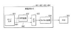
例えば、図25に示したように、車両301のフロント(前方)に車載用カメラ401、左右に車載用カメラ402,403、さらにリア(後方)に車載用カメラ404が設置される。車載用カメラ401〜404はそれぞれ、車内ネットワークを介してECU302(Electrical Control Unit;電子制御ユニット)に接続されている。 For example, as shown in FIG. 25, the vehicle-mounted
車両301のフロントに備え付けられた車載用カメラ401の画像取り込み角度は、例えば図25にaで示す範囲である。車載用カメラ402の画像取り込み角度は、例えば図25にbで示す範囲である。車載用カメラ403の画像取り込み角度は、例えば図25にcで示す範囲である。車載用カメラ404の画像取り込み角度は、例えば図25にdで示す範囲である。車載用カメラ401〜404はそれぞれ、取り込んだ画像をECU302に出力する。この結果、車両301の前方、左右、後方の360度(全方位)の画像をECU302において取り込むことができる。 The image capture angle of the vehicle-mounted
例えば、図26に示したように、車載用カメラ401〜404はそれぞれ、イメージセンサ431と、DSP(Digital Signal Processing)回路432と、セレクタ433と、SerDes(SERializer/DESerializer)回路434とを有している。
For example, as shown in FIG. 26, the in-
DSP回路432は、イメージセンサ431から出力された撮像信号に対して各種の画像信号処理を行うものである。SerDes回路434は、信号のシリアル/パラレル変換を行うものであり、例えばFPD−Link III等の車載インタフェースチップで構成されている。
The
セレクタ433は、イメージセンサ431から出力された撮像信号を、DSP回路432を介して出力するか、DSP回路432を介さずに出力するかを選択するものである。 The
イメージセンサ431とDSP回路432との間の接続インタフェース441に、例えば、上記各実施の形態の通信システムが適用可能である。また、イメージセンサ431とセレクタ433との間の接続インタフェース442に、例えば、上記各実施の形態の通信システムが適用可能である。 For example, the communication system of each of the above embodiments can be applied to the
<6.その他の実施の形態>
本開示による技術は、上記各実施の形態の説明に限定されず種々の変形実施が可能である。<6. Other embodiments>
The technique according to the present disclosure is not limited to the description of each of the above embodiments, and various modifications can be implemented.
例えば、本技術は以下のような構成を取ることができる。
(1)
クロック信号をクロック信号線に出力するクロック信号送信回路と、
データ信号をデータ信号線に出力するデータ信号送信回路と、
前記データ信号のブランキング期間に同期して、前記クロック信号送信回路から前記クロック信号線に、前記クロック信号に代えて所定のブランキング信号が出力されるよう、前記クロック信号送信回路を制御するブランキング制御部と
を備える送信装置。
(2)
前記クロック信号送信回路は、前記クロック信号として差動のクロック信号を前記クロック信号線に出力する差動クロック信号送信回路であり、
前記データ信号送信回路は、前記データ信号として差動のデータ信号を前記データ信号線に出力する差動データ信号送信回路であり、
前記ブランキング制御部は、前記データ信号のブランキング期間の開始時刻に同期して、前記差動クロック信号送信回路から前記クロック信号線に、前記所定のブランキング信号として、所定の期間以上に亘って所定の第1の信号値が連続する差動ブランキング信号が出力されるよう、前記差動クロック信号送信回路を制御する
上記(1)に記載の送信装置。
(3)
前記所定の期間は、前記クロック信号のクロック周期よりも長い期間である
上記(2)に記載の送信装置。
(4)
前記ブランキング制御部は、前記データ信号のブランキング期間の終了時刻に同期して、前記差動クロック信号送信回路から前記クロック信号線に、前記差動ブランキング信号に代えて、前記差動ブランキング信号とは異なる所定の差動信号が出力されるよう、前記差動クロック信号送信回路を制御する
上記(2)または(3)に記載の送信装置。
(5)
前記ブランキング制御部は、前記差動クロック信号送信回路から前記クロック信号線に、前記所定の差動信号として、前記所定の第1の信号値とは異なる所定の第2の信号値が前記所定の期間以上に亘って連続する差動の信号が出力されるよう、前記差動クロック信号送信回路を制御する
上記(4)に記載の送信装置。
(6)
前記ブランキング制御部は、前記差動クロック信号送信回路から前記クロック信号線に、前記所定の差動信号として、前記所定の期間以上に亘って前記クロック信号が出力されるよう、前記差動クロック信号送信回路を制御する
上記(4)に記載の送信装置。
(7)
前記ブランキング制御部は、前記所定の第2の信号値の信号が出力された後、前記差動クロック信号送信回路から前記クロック信号線に、前記ブランキング期間内において前記クロック信号が出力されるよう、前記差動クロック信号送信回路を制御する
上記(5)に記載の送信装置。
(8)
前記ブランキング制御部は、さらに、前記データ信号のブランキング期間の開始時刻に同期して、前記データ信号送信回路から前記データ信号線に、前記データ信号に代えて、少なくとも所定のデータブランキング信号が出力されるよう、前記データ信号送信回路を制御する
上記(2)ないし(7)のいずれか1つに記載の送信装置。
(9)
前記ブランキング制御部は、前記所定のデータブランキング信号として、前記データ信号の最後の信号値を反転した信号が出力されるよう、前記データ信号送信回路を制御する
上記(8)に記載の送信装置。
(10)
前記ブランキング制御部は、前記所定のデータブランキング信号として、値が1となる差動信号が出力されるよう、前記差動データ信号送信回路を制御する
上記(8)に記載の送信装置。
(11)
前記ブランキング制御部は、前記所定のデータブランキング信号が出力された後、前記データ信号のブランキング期間の終了時刻に同期して、値が0となる差動信号が出力されるよう、前記差動データ信号送信回路を制御する
上記(8)に記載の送信装置。
(12)
前記ブランキング制御部は、前記所定のデータブランキング信号として、前記ブランキング期間の全体に亘って値が0となる差動信号が出力されるよう、前記差動データ信号送信回路を制御する
上記(8)に記載の送信装置。
(13)
第1のシングルエンド信号を出力する第1のシングルエンド信号送信回路と、
前記クロック信号線に前記差動クロック信号送信回路と前記第1のシングルエンド信号送信回路とのいずれか一方から信号出力がなされるよう、信号出力の経路を切り替える第1の送信切り替え回路と、
第2のシングルエンド信号を出力する第2のシングルエンド信号送信回路と、
前記データ信号線に前記差動データ信号送信回路と前記第2のシングルエンド信号送信回路とのいずれか一方から信号出力がなされるよう、信号出力の経路を切り替える第2の送信切り替え回路と
をさらに備える
上記(2)ないし(12)のいずれか1つに記載の送信装置。
(14)
データ信号をデータ信号線を介して受信するデータ信号受信回路と、
クロック信号と、前記データ信号のブランキング期間に同期して出力された所定のブランキング信号とを、クロック信号線を介して受信するクロック信号受信回路と
を備える受信装置。
(15)
前記データ信号受信回路は、前記データ信号として差動のデータ信号を前記データ信号線を介して受信する差動データ信号受信回路であり、
前記クロック信号受信回路は、前記クロック信号として差動のクロック信号を受信すると共に、前記所定のブランキング信号として前記データ信号のブランキング期間の開始時刻に同期して所定の期間以上に亘って所定の第1の信号値が連続するように出力された差動ブランキング信号を受信する差動クロック信号受信回路である
上記(14)に記載の受信装置。
(16)
前記差動データ信号受信回路は、
前記データ信号線に接続された終端抵抗を含むデータ信号終端回路を有し、
前記差動クロック信号受信回路は、
前記クロック信号線に接続された終端抵抗を含むクロック信号終端回路と、
前記差動ブランキング信号に基づいて、前記データ信号終端回路および前記クロック信号終端回路に対してそれぞれの前記終端抵抗をオフさせる終端制御回路と
を有する
上記(15)に記載の受信装置。
(17)
前記差動クロック信号受信回路は、さらに、
前記データ信号のブランキング期間の終了時刻に同期して出力された、前記差動ブランキング信号とは異なる所定の差動信号を前記クロック信号線を介して受信し、
前記終端制御回路は、
前記所定の差動信号に基づいて、前記データ信号終端回路および前記クロック信号終端回路に対してそれぞれの前記終端抵抗をオンさせる
上記(16)に記載の受信装置。
(18)
第1のシングルエンド信号を前記クロック信号線を介して受信する第1のシングルエンド信号受信回路と、
前記第1のシングルエンド信号を受信するか否かを切り替える第1の受信切り替え回路と、
第2のシングルエンド信号を前記データ信号線を介して受信する第2のシングルエンド信号受信回路と、
前記第2のシングルエンド信号を受信するか否かを切り替える第2の受信切り替え回路と
をさらに備える
上記(15)ないし(17)のいずれか1つに記載の受信装置。
(19)
クロック信号をクロック信号線に出力し、データ信号をデータ信号線に出力し、データ信号のブランキング期間に同期して、前記クロック信号に代えて所定のブランキング信号を出力する送信装置と、
前記データ信号を前記データ信号線を介して受信し、前記クロック信号と前記所定のブランキング信号とを前記クロック信号線を介して受信する受信装置と
を備える通信システム。
(20)
前記送信装置に前記クロック信号を供給する発振器
上記(19)に記載の通信システム。
(21)
前記送信装置は、
第1のシングルエンド信号を出力する第1のシングルエンド信号送信回路と、
前記クロック信号線に前記クロック信号と前記第1のシングルエンド信号とのいずれか一方の信号出力がなされるよう、信号を切り替える第1の送信切り替え回路と、
第2のシングルエンド信号を出力する第2のシングルエンド送信回路と、
前記データ信号線に前記データ信号と前記第2のシングルエンド信号とのいずれか一方の信号出力がなされるよう、信号を切り替える第2の送信切り替え回路と
を備え、
前記受信装置は、
前記第1のシングルエンド信号を前記クロック信号線を介して受信する第1のシングルエンド信号受信回路と、
前記第1のシングルエンド信号を受信するか否かを切り替える第1の受信切り替え回路と、
前記第2のシングルエンド信号を前記データ信号線を介して受信する第2のシングルエンド信号受信回路と、
前記第2のシングルエンド信号を受信するか否かを切り替える第2の受信切り替え回路と
を備える
上記(19)または(20)に記載の通信システム。
(22)
クロック信号をクロック信号線に出力することと、
データ信号をデータ信号線に出力することと、
前記データ信号のブランキング期間に同期して、前記クロック信号線に、前記クロック信号に代えて所定のブランキング信号を出力することと
を含む信号送信方法。
(23)
データ信号をデータ信号線を介して受信することと、
クロック信号と、前記データ信号のブランキング期間に同期して出力された所定のブランキング信号とを、クロック信号線を介して受信することと
を含む信号受信方法。
(24)
クロック信号をクロック信号線に出力することと、
データ信号をデータ信号線に出力することと、
前記データ信号のブランキング期間に同期して、前記クロック信号線に、前記クロック信号に代えて所定のブランキング信号を出力することと、
前記データ信号を前記データ信号線を介して受信することと、
前記クロック信号と前記所定のブランキング信号とを前記クロック信号線を介して受信することと
を含む通信方法。
For example, the present technology can have the following configuration.
(1)
A clock signal transmission circuit that outputs a clock signal to a clock signal line,
A data signal transmission circuit that outputs a data signal to a data signal line,
A clock signal transmission circuit is controlled so that a predetermined blanking signal is output from the clock signal transmission circuit to the clock signal line in place of the clock signal in synchronization with the blanking period of the data signal. A transmitter equipped with a ranking control unit.
(2)
The clock signal transmission circuit is a differential clock signal transmission circuit that outputs a differential clock signal as the clock signal to the clock signal line.
The data signal transmission circuit is a differential data signal transmission circuit that outputs a differential data signal as the data signal to the data signal line.
The blanking control unit synchronizes with the start time of the blanking period of the data signal from the differential clock signal transmission circuit to the clock signal line as the predetermined blanking signal for a predetermined period or longer. The transmitter according to (1) above, which controls the differential clock signal transmission circuit so that a differential blanking signal having a continuous predetermined first signal value is output.
(3)
The transmitter according to (2) above, wherein the predetermined period is a period longer than the clock period of the clock signal.
(4)
The blanking control unit synchronizes with the end time of the blanking period of the data signal, from the differential clock signal transmission circuit to the clock signal line, and instead of the differential blanking signal, the differential blanking. The transmitter according to (2) or (3) above, which controls the differential clock signal transmission circuit so that a predetermined differential signal different from the ranking signal is output.
(5)
In the blanking control unit, a predetermined second signal value different from the predetermined first signal value is set as the predetermined differential signal from the differential clock signal transmission circuit to the clock signal line. The transmitter according to (4) above, which controls the differential clock signal transmission circuit so that a continuous differential signal is output for a period equal to or longer than the above period.
(6)
The blanking control unit outputs the clock signal from the differential clock signal transmission circuit to the clock signal line as the predetermined differential signal for a period of a predetermined period or longer. The transmitter according to (4) above, which controls a signal transmission circuit.
(7)
The blanking control unit, after the signal of the predetermined second signal value is output to the differential clock signal the clock signal line from the transmission circuit,the clock signal is output within the blanking period The transmitter according to (5) above, which controls the differential clock signal transmission circuit.
(8)
The blanking control unit further synchronizes with the start time of the blanking period of the data signal, from the data signal transmission circuit to the data signal line, and instead of the data signal, at least a predetermined data blanking signal. The transmission device according to any one of (2) to (7) above, which controls the data signal transmission circuit so that
(9)
The transmission according to (8) above, wherein the blanking control unit controls the data signal transmission circuit so that a signal obtained by inverting the last signal value of the data signal is output as the predetermined data blanking signal. apparatus.
(10)
The transmission device according to (8) above, wherein the blanking control unit controls the differential data signal transmission circuit so that a differential signal having a value of 1 is output as the predetermined data blanking signal.
(11)
After the predetermined data blanking signal is output, the blanking control unit outputs a differential signal having a value of 0 in synchronization with the end time of the blanking period of the data signal. The transmitter according to (8) above, which controls a differential data signal transmission circuit.
(12)
The blanking control unit controls the differential data signal transmission circuit so that a differential signal having a value of 0 over the entire blanking period is output as the predetermined data blanking signal. The transmitter according to (8).
(13)
A first single-ended signal transmission circuit that outputs a first single-ended signal,
A first transmission switching circuit that switches a signal output path so that a signal is output to the clock signal line from either the differential clock signal transmission circuit or the first single-ended signal transmission circuit.
A second single-ended signal transmission circuit that outputs a second single-ended signal, and
A second transmission switching circuit that switches the signal output path so that a signal is output from either the differential data signal transmission circuit or the second single-ended signal transmission circuit to the data signal line is further added. The transmitter according to any one of (2) to (12) above.
(14)
A data signal receiving circuit that receives data signals via data signal lines,
A receiving device including a clock signal receiving circuit that receives a clock signal and a predetermined blanking signal output in synchronization with the blanking period of the data signal via a clock signal line.
(15)
The data signal receiving circuit is a differential data signal receiving circuit that receives a differential data signal as the data signal via the data signal line.
The clock signal receiving circuit receives a differential clock signal as the clock signal, and synchronizes with the start time of the blanking period of the data signal as the predetermined blanking signal for a predetermined period or longer. The receiving device according to (14) above, which is a differential clock signal receiving circuit that receives a differential blanking signal output so that the first signal value of the above is continuous.
(16)
The differential data signal receiving circuit
It has a data signal termination circuit including a terminating resistor connected to the data signal line.
The differential clock signal receiving circuit is
A clock signal termination circuit including a terminating resistor connected to the clock signal line,
The receiver according to (15) above, further comprising a data signal terminating circuit and a terminating control circuit that turns off the respective terminating resistors with respect to the clock signal terminating circuit based on the differential blanking signal.
(17)
The differential clock signal receiving circuit further
A predetermined differential signal different from the differential blanking signal, which is output in synchronization with the end time of the blanking period of the data signal, is received via the clock signal line.
The termination control circuit
The receiving device according to (16) above, which turns on the respective terminating resistors for the data signal terminating circuit and the clock signal terminating circuit based on the predetermined differential signal.
(18)
A first single-ended signal receiving circuit that receives a first single-ended signal via the clock signal line, and a first single-ended signal receiving circuit.
A first reception switching circuit that switches whether or not to receive the first single-ended signal, and
A second single-ended signal receiving circuit that receives a second single-ended signal via the data signal line, and a second single-ended signal receiving circuit.
The receiving device according to any one of (15) to (17) above, further comprising a second receiving switching circuit for switching whether or not to receive the second single-ended signal.
(19)
A transmitter that outputs a clock signal to a clock signal line, outputs a data signal to a data signal line, synchronizes with a blanking period of the data signal, and outputs a predetermined blanking signal in place of the clock signal.
A communication system including a receiving device that receives the data signal via the data signal line and receives the clock signal and the predetermined blanking signal via the clock signal line.
(20)
Oscillator that supplies the clock signal to the transmitter The communication system according to (19) above.
(21)
The transmitter is
A first single-ended signal transmission circuit that outputs a first single-ended signal,
A first transmission switching circuit that switches signals so that either one of the clock signal and the first single-ended signal is output to the clock signal line.
A second single-ended transmission circuit that outputs a second single-ended signal,
The data signal line is provided with a second transmission switching circuit for switching signals so that either the data signal or the second single-ended signal is output.
The receiving device is
A first single-ended signal receiving circuit that receives the first single-ended signal via the clock signal line, and a first single-ended signal receiving circuit.
A first reception switching circuit that switches whether or not to receive the first single-ended signal, and
A second single-ended signal receiving circuit that receives the second single-ended signal via the data signal line, and a second single-ended signal receiving circuit.
The communication system according to (19) or (20) above, comprising a second reception switching circuit for switching whether or not to receive the second single-ended signal.
(22)
Outputting the clock signal to the clock signal line and
Outputting a data signal to a data signal line and
A signal transmission method including outputting a predetermined blanking signal in place of the clock signal to the clock signal line in synchronization with the blanking period of the data signal.
(23)
Receiving data signals via data signal lines
A signal receiving method including receiving a clock signal and a predetermined blanking signal output in synchronization with the blanking period of the data signal via a clock signal line.
(24)
Outputting the clock signal to the clock signal line and
Outputting a data signal to a data signal line and
Synchronized with the blanking period of the data signal, a predetermined blanking signal is output to the clock signal line instead of the clock signal.
Receiving the data signal via the data signal line and
A communication method including receiving the clock signal and the predetermined blanking signal via the clock signal line.
本出願は、日本国特許庁において2015年6月15日に出願された日本特許出願番号第2015−120465号、および2015年10月19日に出願された日本特許出願番号第2015−205599号を基礎として優先権を主張するものであり、この出願のすべての内容を参照によって本出願に援用する。 This application refers to Japanese Patent Application No. 2015-120465 filed at the Japan Patent Office on June 15, 2015, and Japanese Patent Application No. 2015-205599 filed on October 19, 2015. It claims priority as a basis and incorporates all content of this application by reference into this application.
当業者であれば、設計上の要件や他の要因に応じて、種々の修正、コンビネーション、サブコンビネーション、および変更を想到し得るが、それらは添付の請求の範囲やその均等物の範囲に含まれるものであることが理解される。 One of ordinary skill in the art can conceive of various modifications, combinations, sub-combinations, and changes, depending on design requirements and other factors, which are included in the appended claims and their equivalents. It is understood that it is.
Claims (21)
Translated fromJapaneseデータ信号をデータ信号線に出力するデータ信号送信回路と、
前記データ信号のブランキング期間に同期して、前記ブランキング期間内において、前記クロック信号送信回路から前記クロック信号線に、前記クロック信号に代えて第1の所定のブランキング信号と前記第1の所定のブランキング信号とは異なる第2の所定のブランキング信号とが出力されるよう、前記クロック信号送信回路を制御するブランキング制御部と
を備え、
前記クロック信号送信回路は、前記クロック信号として差動のクロック信号を前記クロック信号線に出力する差動クロック信号送信回路であり、
前記データ信号送信回路は、前記データ信号として差動のデータ信号を前記データ信号線に出力する差動データ信号送信回路であり、
前記ブランキング制御部は、前記データ信号のブランキング期間の開始時刻に同期して、前記差動クロック信号送信回路から前記クロック信号線に、前記第1の所定のブランキング信号として、所定の期間以上に亘って所定の第1の信号値が連続する差動ブランキング信号が出力されるよう、前記差動クロック信号送信回路を制御する
送信装置。A clock signal transmission circuit that outputs a clock signal to a clock signal line,
A data signal transmission circuit that outputs a data signal to a data signal line,
In synchronism with the blanking period of said data signal,said within the blanking period, to the clock signal line from said clock signal transmission circuit, wherein thefirst predetermined place of the clock signal blanking signaland said first A blanking control unit that controls the clock signal transmission circuit is provided so that asecond predetermined blanking signal different from the predetermined blanking signal is output.
The clock signal transmission circuit is a differential clock signal transmission circuit that outputs a differential clock signal as the clock signal to the clock signal line.
The data signal transmission circuit is a differential data signal transmission circuit that outputs a differential data signal as the data signal to the data signal line.
The blanking control unit performs a predetermined period asthe first predetermined blanking signal from the differential clock signal transmission circuit to the clock signal line in synchronization with the start time of the blanking period of the data signal. A transmission device that controls the differential clock signal transmission circuit so that a differential blanking signal having a continuous predetermined first signal value is output over the above.
請求項1に記載の送信装置。The transmitter according to claim 1, wherein the predetermined period is a period longer than the clock period of the clock signal.
請求項1に記載の送信装置。The blanking control unit synchronizes with the end time of the blanking period of the data signal, and within the blanking period, from the differential clock signal transmission circuit to the clock signal line and to the differential blanking signal. The first aspect of claim 1, wherein the differential clock signal transmission circuit is controlled so that a predetermined differential signal different from the differential blanking signal is output asthe second predetermined blanking signal . Transmitter.
請求項3に記載の送信装置。During the blanking period, the blanking control unit transfersa predetermined differential signal from the differential clock signal transmission circuit to the clock signal line as the predetermined differential signal, which is different from the predetermined first signal value. The transmission device according to claim 3, wherein the differential clock signal transmission circuit is controlled so that a differential signal whose signal value of 2 is continuous for a predetermined period or longer is output.
請求項3に記載の送信装置。During the blanking period, the blanking control unit outputs the clock signal from the differential clock signal transmission circuit to the clock signal line as the predetermined differential signal over the predetermined period or longer. The transmission device according to claim 3, wherein the differential clock signal transmission circuit is controlled so as to control the differential clock signal transmission circuit.
請求項4に記載の送信装置。The blanking control unit,within the blanking period after the signal of the predetermined second signal value is output to the clock signal line from the differential clock signal transmittingcircuit, the clock signal is output The transmission device according to claim 4, wherein the differential clock signal transmission circuit is controlled so as to control the differential clock signal transmission circuit.
請求項1に記載の送信装置。The blanking control unit further synchronizes with the start time of the blanking period of the data signal, from the data signal transmission circuit to the data signal line, and instead of the data signal, at least a predetermined data blanking signal. The transmission device according to claim 1, which controls the data signal transmission circuit so that
請求項7に記載の送信装置。The transmission device according to claim 7, wherein the blanking control unit controls the data signal transmission circuit so that a signal obtained by inverting the last signal value of the data signal is output as the predetermined data blanking signal. ..
請求項7に記載の送信装置。The transmission device according to claim 7, wherein the blanking control unit controls the differential data signal transmission circuit so that a differential signal having a value of 1 is output as the predetermined data blanking signal.
請求項7に記載の送信装置。After the predetermined data blanking signal is output, the blanking control unit outputs a differential signal having a value of 0 in synchronization with the end time of the blanking period of the data signal. The transmission device according to claim 7, which controls a differential data signal transmission circuit.
請求項7に記載の送信装置。The blanking control unit controls the differential data signal transmission circuit so that a differential signal having a value of 0 over the entire blanking period is output as the predetermined data blanking signal. Item 7. The transmitting device according to item 7.
前記クロック信号線に前記差動クロック信号送信回路と前記第1のシングルエンド信号送信回路とのいずれか一方から信号出力がなされるよう、信号出力の経路を切り替える第1の送信切り替え回路と、
第2のシングルエンド信号を出力する第2のシングルエンド信号送信回路と、
前記データ信号線に前記差動データ信号送信回路と前記第2のシングルエンド信号送信回路とのいずれか一方から信号出力がなされるよう、信号出力の経路を切り替える第2の送信切り替え回路と
をさらに備える
請求項1に記載の送信装置。A first single-ended signal transmission circuit that outputs a first single-ended signal,
A first transmission switching circuit that switches a signal output path so that a signal is output to the clock signal line from either the differential clock signal transmission circuit or the first single-ended signal transmission circuit.
A second single-ended signal transmission circuit that outputs a second single-ended signal, and
A second transmission switching circuit that switches the signal output path so that a signal is output from either the differential data signal transmission circuit or the second single-ended signal transmission circuit to the data signal line is further added. The transmitter according to claim 1.
クロック信号をクロック信号線を介して受信すると共に、前記データ信号のブランキング期間に同期して前記ブランキング期間内に出力された、第1の所定のブランキング信号と前記第1の所定のブランキング信号とは異なる第2の所定のブランキング信号とを、クロック信号線を介して受信するクロック信号受信回路と
を備え、
前記データ信号受信回路は、前記データ信号として差動のデータ信号を前記データ信号線を介して受信する差動データ信号受信回路であり、
前記クロック信号受信回路は、前記クロック信号として差動のクロック信号を受信すると共に、前記第1の所定のブランキング信号として前記データ信号のブランキング期間の開始時刻に同期して所定の期間以上に亘って所定の第1の信号値が連続するように出力された差動ブランキング信号を受信する差動クロック信号受信回路である
受信装置。A data signal receiving circuit that receives data signals via data signal lines,
The first predetermined blanking signal andthe first predetermined blanking, whichare received within the blanking period in synchronization with the blanking period of the data signalwhile receiving the clock signal via the clock signal line, are output. It is provided with a clock signal receiving circuit that receives asecond predetermined blanking signal different from the ranking signal via a clock signal line.
The data signal receiving circuit is a differential data signal receiving circuit that receives a differential data signal as the data signal via the data signal line.
The clock signal receiving circuit receives a differential clock signal as the clock signal, and synchronizes with the start time of the blanking period of the data signal asthe first predetermined blanking signal for a predetermined period or longer. A receiving device that is a differential clock signal receiving circuit that receives a differential blanking signal output so that a predetermined first signal value is continuous.
前記データ信号線に接続された終端抵抗を含むデータ信号終端回路を有し、
前記差動クロック信号受信回路は、
前記クロック信号線に接続された終端抵抗を含むクロック信号終端回路と、
前記差動ブランキング信号に基づいて、前記データ信号終端回路および前記クロック信号終端回路に対してそれぞれの前記終端抵抗をオフさせる終端制御回路と
を有する
請求項13に記載の受信装置。The differential data signal receiving circuit
It has a data signal termination circuit including a terminating resistor connected to the data signal line.
The differential clock signal receiving circuit is
A clock signal termination circuit including a terminating resistor connected to the clock signal line,
The receiving device according to claim 13, further comprising a data signal terminating circuit and a terminating control circuit that turns off the respective terminating resistors with respect to the clock signal terminating circuit based on the differential blanking signal.
前記データ信号のブランキング期間の終了時刻に同期して、前記ブランキング期間内に前記第2の所定のブランキング信号として出力された、前記差動ブランキング信号とは異なる所定の差動信号を前記クロック信号線を介して受信し、
前記終端制御回路は、
前記所定の差動信号に基づいて、前記データ信号終端回路および前記クロック信号終端回路に対してそれぞれの前記終端抵抗をオンさせる
請求項14に記載の受信装置。The differential clock signal receiving circuit further
A predetermined differential signal different from the differential blanking signal output asthe second predetermined blanking signal within the blanking period is synchronized with the end time of the blanking period of the data signal. Received via the clock signal line
The termination control circuit
The receiving device according to claim 14, wherein the respective terminating resistors are turned on for the data signal terminating circuit and the clock signal terminating circuit based on the predetermined differential signal.
前記第1のシングルエンド信号を受信するか否かを切り替える第1の受信切り替え回路と、
第2のシングルエンド信号を前記データ信号線を介して受信する第2のシングルエンド信号受信回路と、
前記第2のシングルエンド信号を受信するか否かを切り替える第2の受信切り替え回路と
をさらに備える
請求項13に記載の受信装置。A first single-ended signal receiving circuit that receives a first single-ended signal via the clock signal line, and a first single-ended signal receiving circuit.
A first reception switching circuit that switches whether or not to receive the first single-ended signal, and
A second single-ended signal receiving circuit that receives a second single-ended signal via the data signal line, and a second single-ended signal receiving circuit.
The receiving device according to claim 13, further comprising a second receiving switching circuit for switching whether or not to receive the second single-ended signal.
前記データ信号を前記データ信号線を介して受信し、前記クロック信号と前記第1の所定のブランキング信号と前記第2の所定のブランキング信号とを前記クロック信号線を介して受信する受信装置と
を備え、
前記送信装置は、
第1のシングルエンド信号を出力する第1のシングルエンド信号送信回路と、
前記クロック信号線に前記クロック信号と前記第1のシングルエンド信号とのいずれか一方の信号出力がなされるよう、信号を切り替える第1の送信切り替え回路と、
第2のシングルエンド信号を出力する第2のシングルエンド送信回路と、
前記データ信号線に前記データ信号と前記第2のシングルエンド信号とのいずれか一方の信号出力がなされるよう、信号を切り替える第2の送信切り替え回路と
を有し、
前記受信装置は、
前記第1のシングルエンド信号を前記クロック信号線を介して受信する第1のシングルエンド信号受信回路と、
前記第1のシングルエンド信号を受信するか否かを切り替える第1の受信切り替え回路と、
前記第2のシングルエンド信号を前記データ信号線を介して受信する第2のシングルエンド信号受信回路と、
前記第2のシングルエンド信号を受信するか否かを切り替える第2の受信切り替え回路と
を有する
通信システム。The clock signal is output to the clock signal line, the data signal is output to the data signal line, and in synchronization with the blanking period of the data signal,in place of the clock signalwithin the blanking period, afirst predetermined blank is used. A transmission devicethat outputs aranking signal and a second predetermined blanking signal different from the first predetermined blanking signal to the clock signal line .
A receiving device that receives the data signal via the data signal line, and receives the clock signal,the first predetermined blanking signal, andthe second predetermined blanking signal via the clock signal line. With and
The transmitter is
A first single-ended signal transmission circuit that outputs a first single-ended signal,
A first transmission switching circuit that switches signals so that either one of the clock signal and the first single-ended signal is output to the clock signal line.
A second single-ended transmission circuit that outputs a second single-ended signal,
The data signal line has a second transmission switching circuit that switches signals so that either the data signal or the second single-ended signal is output.
The receiving device is
A first single-ended signal receiving circuit that receives the first single-ended signal via the clock signal line, and a first single-ended signal receiving circuit.
A first reception switching circuit that switches whether or not to receive the first single-ended signal, and
A second single-ended signal receiving circuit that receives the second single-ended signal via the data signal line, and a second single-ended signal receiving circuit.
A communication system including a second reception switching circuit for switching whether or not to receive the second single-ended signal.
をさらに備える
請求項17に記載の通信システム。The communication system according to claim 17, further comprising an oscillator that supplies the clock signal to the transmitter.
差動のデータ信号をデータ信号線に出力することと、
前記データ信号のブランキング期間の開始時刻に同期して、前記ブランキング期間内において、前記クロック信号線に、前記クロック信号に代えて第1の所定のブランキング信号として、所定の期間以上に亘って所定の第1の信号値が連続する差動ブランキング信号を出力することと、
前記第1の所定のブランキング信号が出力された後、前記ブランキング期間内において、前記第1の所定のブランキング信号とは異なる第2の所定のブランキング信号を前記クロック信号線に出力することと
を含む信号送信方法。Outputting a differential clock signal to the clock signal line and
Outputting a differential data signal to a data signal line and
Synchronized with the start time of the blanking period of the data signal, the clock signal line is used asthe first predetermined blanking signal in place of the clock signalwithin the blanking period for a predetermined period or longer. To output a differential blanking signal in which a predetermined first signal value is continuous,
After the first predetermined blanking signal is output, a second predetermined blanking signal different from the first predetermined blanking signal is output to the clock signal line within the blanking period. Signal transmission methods includingthat .
差動のクロック信号をクロック信号線を介して受信することと、
前記データ信号のブランキング期間の開始時刻に同期して、前記ブランキング期間内に所定の期間以上に亘って所定の第1の信号値が連続するように出力された、第1の所定のブランキング信号としての差動ブランキング信号を、前記クロック信号線を介して受信することと、
前記第1の所定のブランキング信号が出力された後、前記ブランキング期間内において出力された、前記第1の所定のブランキング信号とは異なる第2の所定のブランキング信号を前記クロック信号線を介して受信することと
を含む信号受信方法。Receiving differential data signals via data signal lines
Receiving a differential clock signalvia a clock signal line
The data signal in synchronization with the start time of the blankingperiod, the blanking first signal value of a predetermined over more than a predetermined period of timewithin the period is output so as to becontinuous, the first predetermined blanking andthat the differential blanking signal as a rankingsignal, received viathe clock signalline,
After the first predetermined blanking signal is output, the clock signal line is a second predetermined blanking signal output within the blanking period, which is different from the first predetermined blanking signal. signal receiving methodand receiving through.
差動のデータ信号をデータ信号線に出力することと、
前記データ信号のブランキング期間の開始時刻に同期して、前記ブランキング期間内において、前記クロック信号線に、前記クロック信号に代えて第1の所定のブランキング信号として、所定の期間以上に亘って所定の第1の信号値が連続する差動ブランキング信号を出力することと、
前記第1の所定のブランキング信号が出力された後、前記ブランキング期間内において、前記第1の所定のブランキング信号とは異なる第2の所定のブランキング信号を前記クロック信号線に出力することと、
前記データ信号を前記データ信号線を介して受信することと、
前記クロック信号と、前記第1の所定のブランキング信号と、前記第2の所定のブランキング信号とを前記クロック信号線を介して受信することと
を含む通信方法。Outputting a differential clock signal to the clock signal line and
Outputting a differential data signal to a data signal line and
Synchronized with the start time of the blanking period of the data signal, the clock signal line is used asthe first predetermined blanking signal in place of the clock signalwithin the blanking period for a predetermined period or longer. To output a differential blanking signal in which a predetermined first signal value is continuous,
After the first predetermined blanking signal is output, a second predetermined blanking signal different from the first predetermined blanking signal is output to the clock signal line within the blanking period. That and
Receiving the data signal via the data signal line and
A communication method including receiving the clock signal,the first predetermined blanking signal, andthe second predetermined blanking signal via the clock signal line.
Applications Claiming Priority (5)
| Application Number | Priority Date | Filing Date | Title |
|---|---|---|---|
| JP2015120465 | 2015-06-15 | ||
| JP2015120465 | 2015-06-15 | ||
| JP2015205599 | 2015-10-19 | ||
| JP2015205599 | 2015-10-19 | ||
| PCT/JP2016/066556WO2016203987A1 (en) | 2015-06-15 | 2016-06-03 | Transmission device, reception device, communication system, signal transmission method, signal reception method, and communication method |
Publications (2)
| Publication Number | Publication Date |
|---|---|
| JPWO2016203987A1 JPWO2016203987A1 (en) | 2018-04-05 |
| JP6822400B2true JP6822400B2 (en) | 2021-01-27 |
Family
ID=57545617
Family Applications (1)
| Application Number | Title | Priority Date | Filing Date |
|---|---|---|---|
| JP2017524818AActiveJP6822400B2 (en) | 2015-06-15 | 2016-06-03 | Transmitters, receivers, and communication systems, as well as signal transmission methods, signal reception methods, and communication methods. |
Country Status (8)
| Country | Link |
|---|---|
| US (2) | US10419200B2 (en) |
| EP (1) | EP3310012B1 (en) |
| JP (1) | JP6822400B2 (en) |
| KR (1) | KR102451190B1 (en) |
| CN (1) | CN107637035B (en) |
| SG (1) | SG11201708831WA (en) |
| TW (1) | TWI705666B (en) |
| WO (1) | WO2016203987A1 (en) |
Families Citing this family (12)
| Publication number | Priority date | Publication date | Assignee | Title |
|---|---|---|---|---|
| TWI705666B (en)* | 2015-06-15 | 2020-09-21 | 日商新力股份有限公司 | Transmission device, receiving device, communication system |
| JP6838566B2 (en)* | 2016-01-22 | 2021-03-03 | ソニー株式会社 | Transmitter, transmission method, and communication system |
| JP6790435B2 (en)* | 2016-04-20 | 2020-11-25 | ソニー株式会社 | Receivers, transmitters, and communication systems, as well as signal receiving, signaling, and communication methods. |
| US11063652B2 (en)* | 2017-03-07 | 2021-07-13 | Apple Inc. | Techniques for improved beam management |
| TWI809024B (en)* | 2018-01-23 | 2023-07-21 | 日商索尼半導體解決方案公司 | Communication system and communication method |
| TWI658700B (en)* | 2018-07-16 | 2019-05-01 | 創意電子股份有限公司 | Integrated circuit, multi-channels transmission apparatus and signal transmission method thereof |
| US10594367B1 (en)* | 2018-11-07 | 2020-03-17 | Linear Technology Holding Llc | Power over data lines system with accurate and simplified cable resistance sensing |
| CN109817129A (en)* | 2019-01-28 | 2019-05-28 | 武汉精立电子技术有限公司 | A kind of liquid crystal module detection system and method realized based on Mipi CPHY interface |
| DE102019208098B3 (en)* | 2019-06-04 | 2020-08-13 | Continental Automotive Gmbh | Motor vehicle with an antenna network |
| US11031939B1 (en)* | 2020-03-19 | 2021-06-08 | Mellanox Technologies, Ltd. | Phase detector command propagation between lanes in MCM USR serdes |
| WO2022011586A1 (en)* | 2020-07-15 | 2022-01-20 | Intel Corporation | Equalizer settings for a re-driver |
| CN112559421B (en)* | 2020-12-24 | 2023-05-05 | 西安翔腾微电子科技有限公司 | Program control 1394 signal switching circuit |
Family Cites Families (71)
| Publication number | Priority date | Publication date | Assignee | Title |
|---|---|---|---|---|
| JPS63257395A (en)* | 1987-04-14 | 1988-10-25 | Sony Corp | Recorder for color video signal and audio signal |
| JPH0653964A (en)* | 1992-07-31 | 1994-02-25 | Mitsubishi Electric Corp | Serial i/o control system |
| US5815212A (en)* | 1995-06-21 | 1998-09-29 | Sony Corporation | Video overlay circuit for synchronizing and combining analog and digital signals |
| US5974464A (en)* | 1995-10-06 | 1999-10-26 | Silicon Image, Inc. | System for high speed serial video signal transmission using DC-balanced coding |
| US5689309A (en)* | 1996-01-11 | 1997-11-18 | Sony Corporation | Control circuit for mixing two video signals |
| WO1999055082A1 (en)* | 1998-04-17 | 1999-10-28 | Conexant Systems, Inc. | Low cost line-based video compression of digital video stream data |
| US6564269B1 (en)* | 1998-09-10 | 2003-05-13 | Silicon Image, Inc. | Bi-directional data transfer using the video blanking period in a digital data stream |
| US7005938B1 (en)* | 1998-11-09 | 2006-02-28 | Alcatel Usa Sourcing, L.P. | Software controllable termination network for high speed backplane bus |
| JP2001186009A (en)* | 1999-12-22 | 2001-07-06 | Sony Corp | Logic circuit |
| CN1227908C (en)* | 2000-12-18 | 2005-11-16 | 松下电器产业株式会社 | Encryption transmission system |
| JP3903721B2 (en)* | 2001-03-12 | 2007-04-11 | ソニー株式会社 | Information transmitting apparatus and method, information receiving apparatus and method, information transmitting / receiving system and method, recording medium, and program |
| TWI282691B (en)* | 2001-03-23 | 2007-06-11 | Matsushita Electric Industrial Co Ltd | Data-transmission method, data-transmission device, data-reception method and data reception device |
| JP3651409B2 (en)* | 2001-05-14 | 2005-05-25 | セイコーエプソン株式会社 | Semiconductor integrated device and electronic equipment |
| US7558326B1 (en)* | 2001-09-12 | 2009-07-07 | Silicon Image, Inc. | Method and apparatus for sending auxiliary data on a TMDS-like link |
| DE10146742A1 (en)* | 2001-09-22 | 2003-08-21 | Voith Turbo Kg | Method for controlling and / or regulating the drag torque in a drive train and control and regulating system |
| US7519182B2 (en)* | 2002-05-10 | 2009-04-14 | Sony Corporation | Encryption device and decryption device |
| US7006583B2 (en)* | 2002-08-30 | 2006-02-28 | Intel Corporation | Method and apparatus for receiving differential ultra wideband signals |
| US8705571B2 (en)* | 2003-08-13 | 2014-04-22 | Qualcomm Incorporated | Signal interface for higher data rates |
| JP4874113B2 (en)* | 2003-10-22 | 2012-02-15 | エヌエックスピー ビー ヴィ | Method and apparatus for sending and receiving data units via a transmission medium |
| RU2006122542A (en)* | 2003-11-25 | 2008-01-10 | Квэлкомм Инкорпорейтед (US) | HIGH-SPEED DATA TRANSFER INTERFACE WITH IMPROVED COMMUNICATION LINK SYNCHRONIZATION |
| CN1914875A (en)* | 2003-12-08 | 2007-02-14 | 高通股份有限公司 | High data rate interface with improved link synchronization |
| JP3829851B2 (en)* | 2004-03-09 | 2006-10-04 | セイコーエプソン株式会社 | Data transfer control device and electronic device |
| JP4419067B2 (en)* | 2004-07-26 | 2010-02-24 | 株式会社日立製作所 | Semiconductor device, memory device and memory module having digital interface |
| US7522670B2 (en)* | 2005-02-03 | 2009-04-21 | International Business Machines Corporation | Digital transmission circuit and method providing selectable power consumption via single-ended or differential operation |
| US7787526B2 (en)* | 2005-07-12 | 2010-08-31 | Mcgee James Ridenour | Circuits and methods for a multi-differential embedded-clock channel |
| JP2007096266A (en)* | 2005-08-31 | 2007-04-12 | Seiko Epson Corp | Integrated circuit device and electronic apparatus |
| KR100782305B1 (en)* | 2006-01-09 | 2007-12-06 | 삼성전자주식회사 | Data signal transmission / reception apparatus and transmission / reception method by differential signaling of three transmission lines |
| JP4918866B2 (en)* | 2006-03-13 | 2012-04-18 | ミツミ電機株式会社 | COMMUNICATION DEVICE, SEMICONDUCTOR INTEGRATED CIRCUIT DEVICE, AND COMMUNICATION SYSTEM |
| US20070252622A1 (en)* | 2006-04-13 | 2007-11-01 | Hector Saenz | A System for Threshold Reference Voltage Compensation in Pseudo-Differential Signaling |
| JP4371120B2 (en)* | 2006-05-16 | 2009-11-25 | ソニー株式会社 | Image processing apparatus, image processing method, program, and recording medium |
| JP4764354B2 (en)* | 2007-01-10 | 2011-08-31 | 株式会社リコー | Differential signal receiving circuit device |
| US8064535B2 (en)* | 2007-03-02 | 2011-11-22 | Qualcomm Incorporated | Three phase and polarity encoded serial interface |
| US7683673B2 (en)* | 2007-04-24 | 2010-03-23 | National Semiconductor Corporation | Stacked differential signal transmission circuitry |
| KR100871711B1 (en)* | 2007-05-03 | 2008-12-08 | 삼성전자주식회사 | Multiphase Transmit / Receive Circuits Supporting Single-Ended Signaling and Differential Signaling and Clocking Methods for Single-Ended Signaling Transition in Differential Signaling |
| US8107575B2 (en)* | 2007-05-03 | 2012-01-31 | Fairchild Semiconductor Corporation | Method and circuit for changing modes without dedicated control pin |
| JP4517312B2 (en)* | 2008-07-08 | 2010-08-04 | ソニー株式会社 | Memory access control device and imaging device |
| JP5330772B2 (en)* | 2008-08-29 | 2013-10-30 | ルネサスエレクトロニクス株式会社 | Semiconductor integrated circuit and operation method thereof |
| JP5328461B2 (en)* | 2009-04-21 | 2013-10-30 | ルネサスエレクトロニクス株式会社 | Operational amplifier |
| JP5434304B2 (en)* | 2009-06-30 | 2014-03-05 | ソニー株式会社 | Data processing apparatus, data processing method, and program |
| JP5296620B2 (en)* | 2009-07-06 | 2013-09-25 | ルネサスエレクトロニクス株式会社 | Signal relay circuit |
| US8548070B2 (en)* | 2009-11-13 | 2013-10-01 | Panasonic Corporation | Driver circuit, receiver circuit, and method of controlling a communications system including the circuits |
| CN101847134B (en)* | 2010-01-19 | 2012-05-23 | 敦泰科技(深圳)有限公司 | Protocol interface device based on mobile industry processor interface |
| US8713338B2 (en)* | 2010-05-28 | 2014-04-29 | Lsi Corporation | Methods and apparatus for low power out-of-band communications |
| KR101548891B1 (en)* | 2010-11-19 | 2015-09-01 | 샤프 가부시키가이샤 | Data forwarding circuit, data forwarding method, display device, host-side device, and electronic apparatus |
| JP5859219B2 (en)* | 2011-04-22 | 2016-02-10 | 日本オクラロ株式会社 | Differential transmission line and communication device |
| JP6126602B2 (en)* | 2011-08-16 | 2017-05-10 | シリコン・ライン・ゲー・エム・ベー・ハー | Circuit apparatus and method for transmitting signals |
| DE112012003392A5 (en)* | 2011-08-16 | 2014-07-10 | Silicon Line Gmbh | Circuit arrangement and method for transmitting signals |
| WO2013023653A2 (en)* | 2011-08-16 | 2013-02-21 | Silicon Line Gmbh | Circuit arrangement and method for transmitting signals |
| JP6031745B2 (en)* | 2011-10-17 | 2016-11-24 | ソニー株式会社 | Transmitting apparatus, transmitting method, and receiving apparatus |
| EP2772000B1 (en)* | 2011-10-28 | 2020-08-26 | Koninklijke Philips N.V. | Data communication with interventional instruments |
| KR101978937B1 (en)* | 2012-03-16 | 2019-05-15 | 주식회사 실리콘웍스 | A source driver for display device insensitive to power noise |
| US20130265117A1 (en)* | 2012-04-06 | 2013-10-10 | Stanley Yu Tao Ng | Rf and high-speed data cable |
| US9172329B2 (en)* | 2012-08-01 | 2015-10-27 | Nxp B.V. | Harmonic suppression in switching amplifiers |
| US9130557B2 (en)* | 2012-12-03 | 2015-09-08 | Samsung Electronics Co., Ltd. | Operating method of input/output interface |
| US8843093B2 (en)* | 2012-12-20 | 2014-09-23 | Intel Corporation | Low power squelch detector circuit |
| JP6068193B2 (en)* | 2013-02-28 | 2017-01-25 | シナプティクス・ジャパン合同会社 | Reception device and transmission / reception system |
| US9088445B2 (en)* | 2013-03-07 | 2015-07-21 | Qualcomm Incorporated | Method and apparatus for selectively terminating signals on a bidirectional bus based on bus speed |
| US8873644B1 (en)* | 2013-07-30 | 2014-10-28 | Texas Instruments Deutschland Gmbh | Isolated modulator circuit with synchronized pulse generator for self-monitoring reset with capacitively-coupled isolation barrier |
| JP6034273B2 (en)* | 2013-10-04 | 2016-11-30 | ザインエレクトロニクス株式会社 | Transmission device, reception device, transmission / reception system, and image display system |
| TWI543596B (en)* | 2013-12-26 | 2016-07-21 | 晨星半導體股份有限公司 | Multimedia interface receiving circuit |
| JP2015177364A (en)* | 2014-03-14 | 2015-10-05 | シナプティクス・ディスプレイ・デバイス合同会社 | Receiver circuit, display panel driver, display device, and operation method of receiver circuit |
| JP2015211266A (en)* | 2014-04-24 | 2015-11-24 | シナプティクス・ディスプレイ・デバイス合同会社 | Differential amplifier circuit and display drive circuit |
| US9430148B2 (en)* | 2014-05-01 | 2016-08-30 | Avago Technologies General Ip (Singapore) Pte. Ltd. | Multiplexed synchronous serial port communication with skew control for storage device |
| US9697806B2 (en)* | 2014-05-08 | 2017-07-04 | Novatek Microelectronics Corp. | Self-refresh control method, sink device thereof and display system thereof |
| TWI705666B (en)* | 2015-06-15 | 2020-09-21 | 日商新力股份有限公司 | Transmission device, receiving device, communication system |
| US9602317B1 (en)* | 2015-10-12 | 2017-03-21 | Qualcomm Incorporated | Apparatus and method for combining currents from passive equalizer in sense amplifier |
| WO2017100078A1 (en)* | 2015-12-08 | 2017-06-15 | Rambus Inc. | Low power signaling interface |
| US10739812B2 (en)* | 2015-12-11 | 2020-08-11 | Sony Corporation | Communication system and communication method |
| KR102529187B1 (en)* | 2016-03-31 | 2023-05-04 | 삼성전자주식회사 | Reception interface circuit supporting multiple communication standards and memory system including the same |
| JP6790435B2 (en)* | 2016-04-20 | 2020-11-25 | ソニー株式会社 | Receivers, transmitters, and communication systems, as well as signal receiving, signaling, and communication methods. |
| US10425124B1 (en)* | 2018-03-14 | 2019-09-24 | Pericom Semiconductor Corporation | Repeaters with fast transitions from low-power standby to low-frequency signal transmission |
- 2016
- 2016-04-27TWTW105113163Apatent/TWI705666B/enactive
- 2016-06-03SGSG11201708831WApatent/SG11201708831WA/enunknown
- 2016-06-03WOPCT/JP2016/066556patent/WO2016203987A1/ennot_activeCeased
- 2016-06-03CNCN201680033258.9Apatent/CN107637035B/enactiveActive
- 2016-06-03JPJP2017524818Apatent/JP6822400B2/enactiveActive
- 2016-06-03KRKR1020177034704Apatent/KR102451190B1/enactiveActive
- 2016-06-03EPEP16811462.7Apatent/EP3310012B1/enactiveActive
- 2016-06-03USUS15/573,691patent/US10419200B2/enactiveActive
- 2019
- 2019-08-08USUS16/535,675patent/US10944536B2/enactiveActive
Also Published As
| Publication number | Publication date |
|---|---|
| TWI705666B (en) | 2020-09-21 |
| EP3310012A1 (en) | 2018-04-18 |
| KR20180018523A (en) | 2018-02-21 |
| WO2016203987A1 (en) | 2016-12-22 |
| JPWO2016203987A1 (en) | 2018-04-05 |
| US20200127805A1 (en) | 2020-04-23 |
| KR102451190B1 (en) | 2022-10-06 |
| EP3310012B1 (en) | 2022-07-27 |
| US10419200B2 (en) | 2019-09-17 |
| TW201644200A (en) | 2016-12-16 |
| CN107637035B (en) | 2021-03-26 |
| US20180145822A1 (en) | 2018-05-24 |
| US10944536B2 (en) | 2021-03-09 |
| CN107637035A (en) | 2018-01-26 |
| EP3310012A4 (en) | 2019-01-23 |
| SG11201708831WA (en) | 2017-11-29 |
Similar Documents
| Publication | Publication Date | Title |
|---|---|---|
| JP6822400B2 (en) | Transmitters, receivers, and communication systems, as well as signal transmission methods, signal reception methods, and communication methods. | |
| JP6790435B2 (en) | Receivers, transmitters, and communication systems, as well as signal receiving, signaling, and communication methods. | |
| JP6763398B2 (en) | Communication system and communication method | |
| JP2000333081A (en) | CMOS sensor unit with serial data transmission function, imaging unit and image data transmission / reception system using the same | |
| WO2015120149A1 (en) | Increasing throughput on multi-wire and multi-lane interfaces | |
| JP2017195500A5 (en) | ||
| JP7503620B2 (en) | Data transmission device | |
| TW201603503A (en) | Receiver, transmitter and communication system | |
| KR101316179B1 (en) | Duel camera | |
| JP2000200482A (en) | Data input/output circuit and interface system | |
| KR100874671B1 (en) | Apparatus and method for data transmission | |
| US20100201877A1 (en) | Apparatus and method for providing digital multimedia broadcast service using an external device and a digital tv | |
| KR20070041857A (en) | Camera sensor module and method for transmitting encoded data of mobile communication terminal and camera sensor module |
Legal Events
| Date | Code | Title | Description |
|---|---|---|---|
| A521 | Request for written amendment filed | Free format text:JAPANESE INTERMEDIATE CODE: A523 Effective date:20190531 | |
| A621 | Written request for application examination | Free format text:JAPANESE INTERMEDIATE CODE: A621 Effective date:20190531 | |
| A131 | Notification of reasons for refusal | Free format text:JAPANESE INTERMEDIATE CODE: A131 Effective date:20200121 | |
| A521 | Request for written amendment filed | Free format text:JAPANESE INTERMEDIATE CODE: A523 Effective date:20200318 | |
| A131 | Notification of reasons for refusal | Free format text:JAPANESE INTERMEDIATE CODE: A131 Effective date:20200428 | |
| A521 | Request for written amendment filed | Free format text:JAPANESE INTERMEDIATE CODE: A523 Effective date:20200619 | |
| TRDD | Decision of grant or rejection written | ||
| A01 | Written decision to grant a patent or to grant a registration (utility model) | Free format text:JAPANESE INTERMEDIATE CODE: A01 Effective date:20201208 | |
| A61 | First payment of annual fees (during grant procedure) | Free format text:JAPANESE INTERMEDIATE CODE: A61 Effective date:20201221 | |
| R151 | Written notification of patent or utility model registration | Ref document number:6822400 Country of ref document:JP Free format text:JAPANESE INTERMEDIATE CODE: R151 |