JP6822185B2 - Touch panel device and image display device equipped with it - Google Patents
Touch panel device and image display device equipped with itDownload PDFInfo
- Publication number
- JP6822185B2 JP6822185B2JP2017021182AJP2017021182AJP6822185B2JP 6822185 B2JP6822185 B2JP 6822185B2JP 2017021182 AJP2017021182 AJP 2017021182AJP 2017021182 AJP2017021182 AJP 2017021182AJP 6822185 B2JP6822185 B2JP 6822185B2
- Authority
- JP
- Japan
- Prior art keywords
- sensor
- touch
- transparent adhesive
- adhesive material
- touch panel
- Prior art date
- Legal status (The legal status is an assumption and is not a legal conclusion. Google has not performed a legal analysis and makes no representation as to the accuracy of the status listed.)
- Active
Links
Images


Classifications
- G—PHYSICS
- G06—COMPUTING OR CALCULATING; COUNTING
- G06F—ELECTRIC DIGITAL DATA PROCESSING
- G06F3/00—Input arrangements for transferring data to be processed into a form capable of being handled by the computer; Output arrangements for transferring data from processing unit to output unit, e.g. interface arrangements
- G06F3/01—Input arrangements or combined input and output arrangements for interaction between user and computer
- G06F3/03—Arrangements for converting the position or the displacement of a member into a coded form
- G06F3/041—Digitisers, e.g. for touch screens or touch pads, characterised by the transducing means
- G06F3/044—Digitisers, e.g. for touch screens or touch pads, characterised by the transducing means by capacitive means
- G06F3/0446—Digitisers, e.g. for touch screens or touch pads, characterised by the transducing means by capacitive means using a grid-like structure of electrodes in at least two directions, e.g. using row and column electrodes
- G—PHYSICS
- G06—COMPUTING OR CALCULATING; COUNTING
- G06F—ELECTRIC DIGITAL DATA PROCESSING
- G06F3/00—Input arrangements for transferring data to be processed into a form capable of being handled by the computer; Output arrangements for transferring data from processing unit to output unit, e.g. interface arrangements
- G06F3/01—Input arrangements or combined input and output arrangements for interaction between user and computer
- G06F3/03—Arrangements for converting the position or the displacement of a member into a coded form
- G06F3/041—Digitisers, e.g. for touch screens or touch pads, characterised by the transducing means
- G06F3/0412—Digitisers structurally integrated in a display
- G—PHYSICS
- G06—COMPUTING OR CALCULATING; COUNTING
- G06F—ELECTRIC DIGITAL DATA PROCESSING
- G06F3/00—Input arrangements for transferring data to be processed into a form capable of being handled by the computer; Output arrangements for transferring data from processing unit to output unit, e.g. interface arrangements
- G06F3/01—Input arrangements or combined input and output arrangements for interaction between user and computer
- G06F3/03—Arrangements for converting the position or the displacement of a member into a coded form
- G06F3/041—Digitisers, e.g. for touch screens or touch pads, characterised by the transducing means
- G06F3/0416—Control or interface arrangements specially adapted for digitisers
- G06F3/04164—Connections between sensors and controllers, e.g. routing lines between electrodes and connection pads
- G—PHYSICS
- G06—COMPUTING OR CALCULATING; COUNTING
- G06F—ELECTRIC DIGITAL DATA PROCESSING
- G06F3/00—Input arrangements for transferring data to be processed into a form capable of being handled by the computer; Output arrangements for transferring data from processing unit to output unit, e.g. interface arrangements
- G06F3/01—Input arrangements or combined input and output arrangements for interaction between user and computer
- G06F3/03—Arrangements for converting the position or the displacement of a member into a coded form
- G06F3/041—Digitisers, e.g. for touch screens or touch pads, characterised by the transducing means
- G06F3/044—Digitisers, e.g. for touch screens or touch pads, characterised by the transducing means by capacitive means
- G06F3/0445—Digitisers, e.g. for touch screens or touch pads, characterised by the transducing means by capacitive means using two or more layers of sensing electrodes, e.g. using two layers of electrodes separated by a dielectric layer
- G—PHYSICS
- G06—COMPUTING OR CALCULATING; COUNTING
- G06F—ELECTRIC DIGITAL DATA PROCESSING
- G06F2203/00—Indexing scheme relating to G06F3/00 - G06F3/048
- G06F2203/041—Indexing scheme relating to G06F3/041 - G06F3/045
- G06F2203/04107—Shielding in digitiser, i.e. guard or shielding arrangements, mostly for capacitive touchscreens, e.g. driven shields, driven grounds
Landscapes
- Engineering & Computer Science (AREA)
- General Engineering & Computer Science (AREA)
- Theoretical Computer Science (AREA)
- Human Computer Interaction (AREA)
- Physics & Mathematics (AREA)
- General Physics & Mathematics (AREA)
- Computer Networks & Wireless Communication (AREA)
- Position Input By Displaying (AREA)
- Liquid Crystal (AREA)
- Devices For Indicating Variable Information By Combining Individual Elements (AREA)
Description
Translated fromJapanese本発明は、静電容量方式のタッチパネル装置と、それを備えた画像表示装置に関する。 The present invention relates to a capacitance type touch panel device and an image display device including the same.
指などの指示体によるタッチを検出し、そのタッチの位置を示す座標(タッチ座標)を特定するタッチパネル装置は、各種の情報処理装置に広く用いられている。特に、タッチパネルが表示装置の画面上に取り付けられて成るタッチパネル装置は、情報処理装置の新たなユーザーインターフェースとして普及している。A touch panel device that detects a touch by an indicator such as a finger and specifies coordinates (touch coordinates) indicating the position of the touch is widely used in various information processing devices. In particular, a touch panel device in which a touch panel is mounted on the screen of the display device has become widespread as a new user interface for information processing devices.
静電容量方式の1つである投影型静電容量方式は、人の手指が持つ静電容量がタッチパネル内に設けられたタッチセンサに与える僅かな変化を検出回路で検知し、検出結果によりタッチパネル内の位置座標を算出するもので、タッチセンサが内蔵されるタッチパネルの前面側を厚さ数mm程度のガラス板等の保護板で覆った場合でもタッチ検出が可能である。 The projection type capacitance method, which is one of the capacitance methods, detects a slight change in the capacitance of a human finger on a touch sensor provided in the touch panel with a detection circuit, and the touch panel is based on the detection result. It calculates the position coordinates inside, and touch detection is possible even when the front side of the touch panel with a built-in touch sensor is covered with a protective plate such as a glass plate with a thickness of about several mm.
投影型静電容量方式タッチパネル装置は、保護板を前面に配置できるため堅牢性に優れる点、手袋装着時でもタッチ検出が可能である点、可動部が存在しないため長寿命である点などの利点を有している。投影型静電容量方式タッチパネル装置の保護板は、アクリル、ポリカーボネート等の透明樹脂基板やガラス基板等で構成される。手指等の指示体で位置情報を入力するタッチ面の外形サイズを、静電容量を検出するセンサ面より大きくして、センサ面をオーバハングして覆う構造とした場合には、意匠性に優れた製品を提供できる(特許文献1参照)。 The projection type capacitive touch panel device has advantages such as excellent robustness because the protective plate can be placed on the front, touch detection even when wearing gloves, and long life because there are no moving parts. have. The protective plate of the projection type capacitance type touch panel device is composed of a transparent resin substrate such as acrylic or polycarbonate, a glass substrate, or the like. When the external size of the touch surface for inputting position information with an indicator such as a finger is made larger than the sensor surface for detecting capacitance and the sensor surface is overhanged and covered, the design is excellent. A product can be provided (see Patent Document 1).
このようなタッチパネル装置は、手指等の指示体で操作する面がガラスなどになるため、耐久性があり、雨、海水、飲み物、薬品など高誘電物質が付着するような条件で使用されることも多い。投影型静電容量方式タッチパネル装置に要求される性能としては、堅牢性があり手袋装着時などでも高感度な検出が可能な一方で、水分が付着しても誤検出せずに安定に動作することが求められている。 Such a touch panel device is durable because the surface operated by an indicator such as a finger is made of glass, and is used under conditions where highly dielectric substances such as rain, seawater, drinks, and chemicals adhere. There are also many. As for the performance required for the projection type capacitive touch panel device, it is robust and can detect with high sensitivity even when wearing gloves, but it operates stably without erroneous detection even if moisture adheres. Is required.
例えば特許文献2において、水滴等が付着した場合でも誤検出を抑制したタッチパネル装置が開示されている。 For example,
投影型静電容量方式タッチパネル装置の構造において、タッチセンサが内蔵されるタッチパネル基板と、保護板の間は透明粘着材(Optical Clear Adhesive 一般にOCAと略称すこともある)で貼り合わされることが多く、その透明粘着材はアクリル系の樹脂などで比誘電率が3〜6程度と透湿度が50〜300g/m2・24hr程度のものが一般に使用されている。 In the structure of a projection type capacitance type touch panel device, the touch panel substrate in which the touch sensor is built and the protective plate are often bonded with a transparent adhesive material (Optical Clear Acrylic, which is also abbreviated as OCA). As the transparent adhesive material, an acrylic resin or the like having a relative permittivity of about 3 to 6 and a water permeability of about 50 to 300 g / m2 / 24 hr is generally used.
透明粘着材の比誘電率は温度により変化し、室温状態に対し、低温(−30℃)や高温(70℃)の環境では40%も低下するものもあり、水分を吸湿することで変化する場合もあり、タッチパネルセンサで計測される静電容量を変化させる原因となる。 The relative permittivity of the transparent adhesive material changes depending on the temperature, and in some cases it decreases by 40% in a low temperature (-30 ° C) or high temperature (70 ° C) environment with respect to the room temperature state, and it changes by absorbing moisture. In some cases, it causes a change in the capacitance measured by the touch panel sensor.
また、透明粘着材が吸湿する水分は保護ガラス(保護板)やタッチセンサパネルで覆われていない外気(空気)に露出した部分から入るため、その影響は周辺部から変化し、比誘電率は透明粘着材面内で分布を持つことになる。よって透明粘着材の比誘電率の変化による影響は、タッチパネルのタッチ領域の自己容量や相互容量のみならず、タッチパネル面の外周部の影響も受け易く、タッチパネルセンサに外周に沿って配線されたタッチセンサパネルの引出し配線もその影響を受けることとなる。 In addition, since the moisture absorbed by the transparent adhesive enters from the part exposed to the outside air (air) that is not covered by the protective glass (protective plate) or touch sensor panel, the effect changes from the peripheral part, and the relative permittivity changes. It will have a distribution within the surface of the transparent adhesive material. Therefore, the influence of the change in the relative permittivity of the transparent adhesive material is easily affected not only by the self-capacity and mutual capacity of the touch area of the touch panel but also by the outer peripheral portion of the touch panel surface, and the touch wired along the outer periphery of the touch panel sensor. The lead-out wiring of the sensor panel will also be affected.
特に、手袋等の使用に対応した高感度タッチパネル装置においては、指示体により検出する静電容量が非常に小さいため、相対的に透明粘着材の比誘電率の変化による影響が大きくなる。特許文献1に開示されるタッチパネル装置は、水等の比誘電率が非常に高い(比誘電率80程度)物質が保護ガラスに付着した際のタッチセンサと表示装置の金属フレーム等の導電体間の静電容量結合の変化を抑え、タッチパネルの誤検出を抑制する。 In particular, in a high-sensitivity touch panel device compatible with the use of gloves and the like, the capacitance detected by the indicator is very small, so that the influence of the change in the relative permittivity of the transparent adhesive material is relatively large. The touch panel device disclosed in
しかしながら、静電容量結合の変化を抑える手段として、導電性電極で構成された黒枠印刷を持つ保護ガラスとその導電性電極を駆動する回路が必要であるため部品コストが増加するという課題があった。また、透明粘着材の吸湿における影響については特に考慮されていない。 However, as a means of suppressing the change in the capacitance coupling, there is a problem that the component cost increases because a protective glass having a black frame printing composed of conductive electrodes and a circuit for driving the conductive electrodes are required. .. In addition, the effect of the transparent adhesive on moisture absorption is not particularly considered.
本発明は上記のような問題点を解消するためになされたものであり、保護板を採用した場合でも手袋操作などに対応した高感度で、高温高湿条件下での使用に適したタッチパネル装置と、それを有した画像表示装置を提供することを目的とする。さらに厚い保護板や画像表示モジュールに金属フレームを採用するなどにより堅牢性を有するとともに、水滴等が付着した場合でも誤検出を抑制するタッチパネル装置と、それを有した画像表示装置を提供することを目的とする。 The present invention has been made to solve the above-mentioned problems, and is a touch panel device suitable for use under high temperature and high humidity conditions with high sensitivity corresponding to glove operation even when a protective plate is adopted. An object of the present invention is to provide an image display device having the same. To provide a touch panel device that has robustness by adopting a metal frame for a thicker protective plate and an image display module, and suppresses false detection even if water droplets adhere, and an image display device having the touch panel device. The purpose.
この発明に係るタッチパネル装置は、基板上に複数本のセンサが形成されたタッチセンサパネルと、そのタッチセンサパネルを保護する保護板と、前記タッチセンサパネルと前記保護板とを貼り合せる透明粘着材と、その透明粘着材より透湿度が低い防湿シール材と、を備え、前記透明粘着材は、その周囲に前記保護板または前記タッチセンサパネルと接していない領域を有し、前記周囲の少なくとも一部において前記領域が前記防湿シール材で覆われており、前記タッチセンサパネルは、指示体がタッチするセンサ領域と、そのセンサ領域の外周部に複数本のセンサを外部回路に接続するための配線が形成された引き出し配線領域と、を含み、前記透明粘着材は前記センサ領域を覆い、前記基板と前記保護板との間の前記引き出し配線領域の上部に空間を有すること特徴とする。The touch panel device according to the present inventionis a touch sensor panelin which a plurality of sensorsare formedon asubstrate, a protective plate that protects the touch sensor panel, and a transparent adhesive material that adheres the touch sensor panel and the protective plate. And a moisture-proof sealing materialhaving a moisture permeability lower than that of the transparent adhesive material, the transparent adhesive material has a regionaround the transparent adhesive material that is not in contact with the protective plate or the touch sensor panel, andat least one of the surrounding areas.The area is covered with the moisture-proof sealing material,and the touch sensor panel is a wiring for connecting a plurality of sensors to an external circuit in a sensor area touched by an indicator and an outer peripheral portion of the sensor area. The transparent adhesive material covers the sensor area and has a space above the lead-out wiring area between the substrate and the protective plate .
本発明によれば、保護板およびタッチセンサパネルと密着していない領域の一部を防湿シール材で覆うことで、高湿度環境における静電容量方式タッチパネル装置のタッチ座標検出動作時の誤検出を抑制することが可能となる。また保護板の外周部に高誘電物質が付着した際のタッチ座標の誤検出を減らすことができる。
According to the present invention, by covering a part of the area that is not in close contact with the protective plate and the touch sensor panel with a moisture-proof sealing material, erroneous detection during the touch coordinate detection operation of the capacitive touch panel device in a high humidity environment can be detected. can be suppressed andthat Donot. In addition, it is possible to reduce erroneous detection of touch coordinates when a highly dielectric substance adheres to the outer peripheral portion of the protective plate.
実施の形態1.
本発明の実施の形態ついて以下に図面を参照して説明する。以下の説明は、本発明の好適な実施の形態を示すものであって、本発明の範囲が以下の実施の形態に限定されるものではない。以下の説明において、同一の符号が付されたものは実質的に同様の内容を示している。
Embodiments of the present invention will be described below with reference to the drawings. The following description shows preferred embodiments of the present invention, and the scope of the present invention is not limited to the following embodiments. In the following description, those having the same reference numerals indicate substantially the same contents.
実施の形態1.
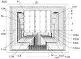
図1は、実施の形態1に係る投影型タッチパネル装置100の構造を示す上面図である。図2は図1に示したタッチパネル装置100の図中に一点鎖線で示した部分(A−A間)の断面図である。図1のように、投影型タッチパネル装置100は、タッチセンサパネル1、保護板2、透明粘着材3、防湿シール材4、フレキシブル配線基板(Flexible Printed Circuit 以後、FPCと略称する)5を含む構成となっている。
FIG. 1 is a top view showing the structure of the projection type
図は説明に必要なタッチパネル装置100を模式的に記載しており、タッチパネル装置100として必要であっても、説明に必要のないタッチパネルコントローラ基板、画像表示モジュール(本実施の形態では液晶表示装置)、ホスト機器およびケーブル類等の図示は省略している。 The figure schematically describes the
タッチセンサパネル1は、タッチを検出するためのセンサとして、垂直方向に伸延し水平方向に並べて配設された複数のXセンサ101(X方向の座標検出用センサ)と、水平方向に伸延し垂直方向に並べて配設された複数のYセンサ102(Y方向の座標検出用センサ)とを備えている。すなわち、複数のXセンサ101および複数のYセンサ102が、互いに直交するように配置されている。説明を簡単にするために、センサ構成は図中に示すようにXセンサ(X0〜X4)=5本,Yセンサ(Y0〜Y3)=4本で記載している。各センサには、タッチセンサパネル1が貼り付けられる液晶表示モジュールのコモン電極など、画像表示モジュールとの間に寄生する自己容量Cgと、Xセンサ−Yセンサ間には相互容量Cmが存在する。 As a sensor for detecting touch, the
タッチセンサパネル1の各センサは、タッチセンサパネルのタッチ領域の外周部(引出し配線領域14)に引き出し配線を持ち、その外周に沿って配線され、一点鎖線で示した端子部105に接続される。Yセンサ用引き出し配線103とXセンサ配線用引き出し配線107の間には、Xセンサ−Yセンサ間の電極間に寄生する容量の影響をシールドするためのシールド配線106、Yセンサ配線用引き出し配線103からタッチセンサパネルの外周側には、Yセンサ−その他近傍の電極間に寄生する容量の影響をシールドするためのシールド配線104が設けられている。端子部105の各センサ配線は、破線で示したFPC5を介してタッチパネルコントローラ(非図示)に接続される。
Each sensor of the
タッチパネルコントローラは、静電容量を計測する回路を内蔵し、各センサの自己容量または相互容量を計測し、指などの指示体が保護板に接触したことによる静電容量の変化を検出する。 The touch panel controller has a built-in circuit for measuring capacitance, measures the self-capacitance or mutual capacitance of each sensor, and detects a change in capacitance due to contact of an indicator such as a finger with a protective plate.
また、タッチパネルコントローラは、その検出結果から内蔵された演算回路を用いて指示体の位置を特定し、ホスト機器(非図示)に指示体のタッチの有無および座標を示すタッチ情報等を送信する手段を備える。 Further, the touch panel controller is a means for identifying the position of the indicator using the built-in arithmetic circuit from the detection result and transmitting touch information indicating the presence / absence of touch of the indicator and coordinates to the host device (not shown). To be equipped.
タッチセンサパネル1のセンサ(101、102)はガラス基板やフィルム基板上に、透明導電膜(ITO:Indium Tin Oxide)または銅やアルミなどの数マイクロメートル幅の金属極細配線を透過率80%以上となるように配置した電極などを成膜したものが多く、Xセンサ101、Yセンサ102間の層間膜や保護絶縁膜を含んだ構造となっている。また、Xセンサ101およびYセンサ102を保護するため、その上部が薄い保護膜で覆われている。
The sensors (101, 102) of the
タッチセンサパネル1は堅牢性を維持するため、ガラスを化学強化処理などで堅牢性、耐傷性を向上させた保護板2と空気層を含まないように透明粘着材3で貼り合わされる。透明粘着材3はアクリル系の樹脂などで、比誘電率が3〜6程度であり、透湿度が50〜300[g/m2・24hr]程度のものが一般的である。 In order to maintain the toughness of the
透明粘着材3は、湿度管理された環境下で貼り合わされ、透明粘着材3とタッチセンサパネル1が密着する面と、透明粘着材3と保護板2が密着する面以外の外気に触れる面(周囲4辺)を防湿シール4で密閉される。 The transparent
以上のタッチパネル装置100は画像表示モジュール(非図示)の金属フレーム6に両面テープ9で貼り合わされている。(その他の事例として、外光反射を低減したり、画像表示モジュールの透過率を上げたりするために、タッチパネル装置―画像表示モジュール間も透明粘着材で貼り合せてもよい)
The
防湿シール4には透湿度が透明粘着材3に対し十分に低く、比誘電率も透明粘着材3より小さいものが望ましい。具体的にはポリオレフィン樹脂が主成分のChase社のヒューミシール(HumiSeal 1B58LU)等を使用する。HumiSeal 1B58LUの透湿度は6.0[g/m2・24h]と、一般的な透明粘着材の1/10〜1/50と非常に小さく、比誘電率も2.0と十分に小さい。 It is desirable that the moisture-
次に、透明粘着材の比誘電率が変化した場合の影響について説明する。図3は図2の断面図の一部を模式的に表したものである。Xセンサ101−Yセンサ102間の相互容量(Mutual capacitance)を計測する場合、Yセンサ102に励起信号(100KHz程度の矩形波など)を印加し、Xセンサ101から図示しない静電容量検出回路(積分回路とアンプ、アナログ−デジタル変換回路(A/D)等で構成される)で計測する。センサX101とYセンサ102は、タッチ検出の感度を上げるために、センサ間の重なる面積が小さく、平面に並んだ面積を大きく配置したセンサのため、Xセンサ101とYセンサ102間の電気力線は符号10aおよび10bで示したように電界が広がり、それらのセンサ間の相互容量は、Xセンサ101とYセンサ102直上の誘電体の影響を受ける。 Next, the effect of changing the relative permittivity of the transparent adhesive material will be described. FIG. 3 is a schematic representation of a part of the cross-sectional view of FIG. When measuring the mutual capacitance between the
センサ直上には透明粘着材3があり、その上には保護板2があるため、透明粘着材3と保護板2の両方の誘電体の影響を受ける。それぞれの厚みにもよるが、センサ直上の誘電体は透明粘着材3のため、透明粘着材3の比誘電率が変化すると、Xセンサ101とYセンサ102間の相互容量も変化する。 Since there is a transparent
図3のXセンサ101とYセンサ102間の相互容量は、GNDに接続されているシールド配線104の影響も僅かに受けており、その影響も透明粘着材3の比誘電率の変化の影響を受ける。 The mutual capacitance between the
静電容量方式のタッチパネル装置では、指示体(非図示)がタッチしていない状態でも、各センサには一定の寄生容量があるため、指示体がタッチしていない状態で計測した値を基準値(ベースライン)とし、各時刻の計測値と基準値との差分値を指示体のタッチによる静電容量変化とみなしてタッチの有無、位置座標を計算する。 In the capacitance type touch panel device, even when the indicator (not shown) is not touched, each sensor has a certain parasitic capacitance, so the value measured when the indicator is not touched is used as the reference value. (Baseline), the difference between the measured value at each time and the reference value is regarded as the change in capacitance due to the touch of the indicator, and the presence / absence of touch and the position coordinates are calculated.
厚い手袋を使用した状態でも操作できる高感度なタッチパネル装置100において、指示体に意図された操作以外による静電容量の変化は、可能な限り小さいことが望ましい。 In the high-sensitivity
高感度なタッチパネル装置100で安定な動作を行うには、透明粘着材3の比誘電率の変化も小さいことが望ましいので、透明粘着材3が湿度の影響を受けないように防湿シール材4で外気を遮断することは、高湿度環境下のタッチパネル検出動作を安定させることにつながる。 In order to perform stable operation with the high-sensitivity
図3では、Xセンサ101とYセンサ102間の相互容量を説明したが、タッチセンサパネル1の外周部に沿って配線されるYセンサ用引き出し配線103とシールド配線104間も同様に配線直上の透明粘着材3の影響を受ける場合がある。
Although the mutual capacitance between the
なお、透明粘着材3は図3の矢印方向から見た側面が外気に曝されているので、外気に含まれる水分が透明粘着材3内部に吸収されていく。 Since the side surface of the transparent
<比較>
図4は防湿シール材4を塗布して外気を遮断した場合(図4の(b))と、塗布を行わず外気を遮断しなかった場合(図4の(a))との、高温高湿試験(Ta=60°C、90%RH、500時間)実施後のタッチパネル装置100の相互容量値の計測結果を示す。図4において、タッチセンサパネル1は、Xセンサ27本(X0〜X26)、Yセンサ16本(Y0〜Y15)がマトリクス状に交差するタッチセンサである。図4の(a)から明らかなように、タッチパネル装置100の相互容量値は面内で均一ではなく、四隅が最も相互容量が大きい分布を持つことが分かる。この測定結果から、高温高湿試験実施後の透明粘着材3の比誘電率は面内で均一ではなく、四隅が最も比誘電率が大きい分布を持つことが分かる。この分布は、透明粘着材3が4辺(図1上の上下左右)を外気に曝されているため、四隅がもっとも水分を吸収し、中心部の吸湿量が少ない状態となり、その結果、中心に向かって相互容量値が減衰する測定結果が得られたのである。<Comparison>
FIG. 4 shows high temperatures and high temperatures when the moisture-
一方、図4の(b)は、防湿シール材4を塗布して透明粘着材3が4辺(上下左右)を外気から遮断し、その後高温高湿試験実施した後のタッチパネル装置100の相互容量値を計測した結果である。図4の(a)と比較すれば明らかなように、タッチパネル装置100の相互容量値は、面内での変動が比較的少なく、四隅と比較しても中心部の落ち込みも少ないことが分かる。これは、防湿シール材4の塗布により、透明粘着材3への水分の吸収が抑えられた結果である。 On the other hand, in FIG. 4B, the mutual capacity of the
図1中の破線で示したセンサ領域11面内での相互容量は、図4の(a)に図示したように、その容量分布の影響を受け、中心部と比較して外周部の容量が高くなる。この変化量がタッチパネルコントローラの静電容量検出範囲(ダイナミックレンジ)に対し無視できない大きさとなった場合、タッチ操作による容量変化に誤差が生じて座標誤差が増加する。また、影響がさらに大きい場合は検出回路がオーバレンジしてタッチしても検出回路がその変化を捉えられず、タッチを検出できないことになる。 As shown in FIG. 4A, the mutual capacitance within the 11 planes of the sensor region shown by the broken line in FIG. 1 is affected by the capacitance distribution, and the capacitance of the outer peripheral portion is larger than that of the central portion. It gets higher. When this amount of change becomes a size that cannot be ignored with respect to the capacitance detection range (dynamic range) of the touch panel controller, an error occurs in the capacitance change due to the touch operation and the coordinate error increases. Further, when the influence is further large, even if the detection circuit overranges and touches, the detection circuit cannot catch the change and the touch cannot be detected.
逆に、透明粘着材3が水分を十分に吸湿した状態から、乾燥した環境に曝された場合は外周部から水分吸収量が減少し、図4の(a)の容相容量分布を反転させたような中心部の容量値が多く、外周部が少なくなることもある。この場合においても、センサ領域11面内の相互容量の分布はこの影響を受け同様にタッチパネル装置100の容量検出動作に影響を与える。 On the contrary, when the transparent
上述の比較結果から明らかなように、本実施の形態のタッチパネル装置100では防湿シール材4で外気を遮断し透明粘着材3の水分吸湿を防ぎ、透明粘着材3の比誘電率の変化を抑制し、透明粘着材3の影響によるタッチセンサパネル1の各センサ(101、102)の自己容量と、各センサ間の相互容量の変化を小さくし高温高湿環境下でのタッチパネルのタッチ座標検出動作を安定させることができる。 As is clear from the above comparison results, in the
なお、実施の形態1では便宜上、Xセンサ101とYセンサ102がマトリクス状となるタッチセンサパネル1を用いて説明したが、タッチパネル面内にタッチ電極を複数配置したセグメント型のタッチパネルにおいても同様の効果がある。 In the first embodiment, for convenience, the
また、防湿シール材4は透明粘着材3が外気と曝される4辺すべてに対し塗布することが最も効果的である。しかしながら、外気と接触する面積が小さいFPC5と保護板2との隙間などはシールを省略しても一定の効果がある。 Further, it is most effective to apply the moisture-
更に、引出し配線(103、107)とシールド配線(104、106)間、引出し配線(103、107)と金属フレーム6間の寄生容量の影響が大きい場合には、影響が大きい引出し配線(103、107)に沿った面のみをシールする構成としても費用対効果が大きい場合もある。 Further, when the influence of the parasitic capacitance between the drawer wiring (103, 107) and the shield wiring (104, 106) and between the drawer wiring (103, 107) and the
すなわち、保護板2またはタッチセンサパネル1と接していない領域の少なくとも一部を防湿シール材4で覆うことにより、高温高湿環境下でのタッチパネル装置100の座標検出動作を安定させることが期待できる。 That is, by covering at least a part of the area not in contact with the
本実施の形態では、タッチセンサパネル1のXセンサ101、Yセンサ102間の層間膜や保護絶縁膜および、Xセンサ101およびYセンサ102を保護するための保護絶縁膜として膜厚が1umの二酸化ケイ素膜(SiO2)使用した。このように層間膜や保護絶縁膜が薄い構造の場合は、透明粘着材3の誘電率の変化の影響を大きく受ける。この場合の防湿シール材4塗布による透明粘着材3の比誘電率の変化抑制の効果は大きい。近年は、タッチセンサパネル1の静電気破壊の耐性を向上するために、保護絶縁膜を厚くする場合があるが、その膜厚として2um以下であっても、透明粘着材3の影響によるタッチセンサパネル1の各センサ(101、102)の自己容量と、各センサ間の相互容量の変化を小さくし高温高湿環境下でのタッチパネルのタッチ座標検出動作を安定させることができる。
In this embodiment,
一方、タッチセンサパネル1の構成として、Xセンサ101を形成したガラス板とYセンサ102を形成したガラス板を貼り合せたガラス2枚で構成した場合、各センサの直上はガラスとなり、透明粘着材3の誘電率の変化の影響は受けにくいが、防湿シール材4の塗布による透明粘着材3の比誘電率の変化抑制の効果は上記二酸化ケイ素膜の場合と同様に有り、タッチセンサパネル1の各センサの自己容量と、各センサ間の相互容量の変化を小さくし、高温高湿環境下でのタッチパネルのタッチ座標検出動作を安定させる効果が期待できる。 On the other hand, when the
実施の形態2.
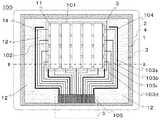
図5は、実施の形態2に係るタッチパネル装置100の構造を示す上面図である。図6は図5に示したタッチパネル装置100の図中に一点鎖線で示した部分(B−B間)の断面図である。本実施の形態のタッチパネル装置100は、図1の構成に対し、透明粘着材3が破線で示したセンサ領域11を覆う大きさで、引出し配線領域14の一部を覆わない位置に貼り合わされている点のみが異なっている。よって、タッチセンサパネル1のセンサ領域11直上は透明粘着材3で覆われ、引出し配線領域14の一部は透明粘着材3で覆われていない空間12を有する構造となる。
FIG. 5 is a top view showing the structure of the
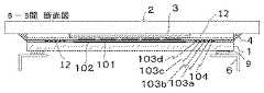
図7は図6の断面図の一部を模式的に表した図に、指示体7でタッチした状態と保護板の外周部に水8(塩水,飲み物,薬品等の高誘電物質)が付着した際の外周センサと画像表示モジュール(非図示)の金属フレーム6間の寄生容量の等価回路を重ねた概略図である。 FIG. 7 is a diagram schematically showing a part of the cross-sectional view of FIG. 6, in which water 8 (high dielectric material such as salt water, drink, chemicals, etc.) adheres to the state of being touched by the
図7aは実施の形態1のタッチパネル、図7bは実施の形態2のタッチパネルを表している。図7において、指示体(指)7でタッチした状態と、高い誘電率(約80)の水8が付着した状態の両方を模擬している。指示体(指)7は、タッチセンサパネル1のXセンサ101aとの間に容量を形成していることを表している。指示体7とタッチセンサパネル1のXセンサ101aには保護板2と透明粘着材3があるため、形成された容量は保護板による容量701aと透明粘着材701bが直列に接続された容量となる。 FIG. 7a shows the touch panel of the first embodiment, and FIG. 7b shows the touch panel of the second embodiment. In FIG. 7, both the state of being touched by the indicator (finger) 7 and the state of being attached with
この容量は、センサ101aの幅や指示体の状態(保護板との接触面積、手袋の有無など)や保護板や透明粘着材の厚みや比誘電率によって異なるが、概ね1pFより小さくなることが多い。特に軍手などの厚い手袋での操作においては、その値は更に1/3程に減少する。この指示体7が存在する場合と、しない場合の差による容量変化がタッチの有無の判定及びタッチ領域内の指位置の計算に使用される。 This capacity varies depending on the width of the
図7において符号702は指示体7の人体容量で、体の体積にもよるが一般的に40〜100pF程度で、指示体7とXセンサ101a間容量に対し、10倍以上と十分に大きいため、実質的にはGNDに接地されていると見なすことができる。 In FIG. 7,
高い誘電率(約80)の水8が付着した場合、水8を介して容量結合するため、保護板の外周部に水8が付着した際の最外周Xセンサ101bの自己容量(Cg101b)は、図中のC801a、C801b、C801c、C801d、C801eが直列接続された静電容量に比例することになる。なお、容量801aは最外周のXセンサ101bと保護板2間、容量C801bと801cは保護板2と水8間、容量801dは保護板2とタッチセンサパネル1間、容量801eは透明粘着材3と金属フレーム6間の容量である。 When
高い誘電率(約80)の水8が付着した場合に形成された最外周のXセンサ101bと金属フレーム6間の容量が、指示体7によるタッチの有無の判定する閾値を越えた場合、水8による影響と指によるタッチとが識別できないため、誤検出の原因となる。指示体7によるタッチの有無の判定する閾値は、手袋操作に対応する高感度タッチパネルの場合、更に小さく設定されるため、相対的に水8付着による影響は特に大きくなる。 When the capacitance between the outermost X sensor 101b and the
実施の形態1では金属フレーム6と重なるタッチパネルセンサ1直上は透明粘着材3(比誘電率およそ3〜6)であるが、実施の形態2ではその領域には、透明粘着材3は無く、空間12であり、その比誘電率は1の空気となるため、C801dは実施の形態2の方が小さくなる。そのため水8付着の影響による最外周Xセンサ101b−金属フレーム6間の寄生容量は空間12によって減少する。 In the first embodiment, the transparent adhesive material 3 (relative permittivity of about 3 to 6) is directly above the
図8は実施の形態1と実施の形態2のタッチパネルで、保護板2の外周部に水8が付着した際(付着した面積は直径7mmの円の2倍)の最外周Xセンサ101bと画像表示モジュールの金属フレーム6間の寄生容量値を、擬似指の感度を基準に相対比でグラフ化したものである。図8の符号13aは、ガラス製の0.7mm厚保護板2(比誘電率5.8)と0.5mm厚のタッチセンサパネル1(比誘電率5.8)と0.2mm厚の透明粘着材3(比誘電率5.8)で構成されたタッチパネル装置100に擬似指7(直径7mmの円で接触する真鍮棒)を配置した場合の自己容量値である。 FIG. 8 shows the touch panels of the first and second embodiments, and an image of the outermost X sensor 101b when
その自己容量値を100%として正規化して、保護板2の外周部に水8が付着した際(付着した面積は直径7mmの円の2倍)の最外周Xセンサ101bと画像表示モジュールの金属フレーム6間の寄生容量値とを比較すると、図8中の符号13bで示した実施の形態1における寄生容量値は56%、符号13cで示した本実施の形態2では43%と金属フレーム6と重なるタッチパネルセンサ1の直上の透明粘着材3を無くすことにより、寄生容量が13%と減少することを表している。
Normalizing the stray capacitance value as 100%, when
この効果は厚い手袋操作に対応するなど、タッチパネル装置100を高感度化するためにタッチを判定する閾値を下げて使用した場合において、水8が付着時の誤検出率を下げる効果がある。また、図7には記載していないが、水8の付着の影響による最外周Xセンサと、シールド配線(104、106)(タッチセンサパネル内のGND電位)との寄生容量も実施の形態2では透明粘着材3が無いため同様に減少する。 This effect has the effect of lowering the erroneous detection rate when
以上により、実施例2では実施例1の効果に加え、保護板2の外周部に水8が付着した際のタッチ座標の誤検出を減らすことが可能なタッチパネル装置100を提供できる。 As described above, in the second embodiment, in addition to the effect of the first embodiment, it is possible to provide the
上述の実施の形態1および実施の形態2において、防湿シール材4はポリオレフィン樹脂が主成分のChase社のヒューミシール(徹湿度は6.0[g/m2・24h])を採用したが、透明粘着材3が外気に曝されている部分を透明粘着材3の透湿度より低い材料で密閉すればよいので、例えば日立化成のFPC用防湿絶縁材料 タッフィー(50g/m2・24h (40℃/90%RH))等でも同様の効果が期待できる。また、塗布型ではなく、カプトンテープなどのポリイミドフィルムテープを透明粘着材3が外気に触れないように4辺に覆うように貼ることでも同様の効果が期待できる。 In the above-described first and second embodiments, the moisture-
さらに、上述の実施の形態1および実施の形態2において、タッチパネル装置―画像表示モジュール間を、両面テープに代えて透明粘着材で貼り合せてもよい。この場合、貼り合せに用いた透明粘着材の、画像表示モジュールまたはタッチセンサパネルに接していない4辺(図1上の上下左右)が外気に曝されることになる。この外気に曝された4辺からの透明粘着材への水分吸湿を防ぐためには、その4辺を透湿度が低い防湿シール材で覆えばよいことは無論である。
Further, in the above-described first and second embodiments, the touch panel device and the image display module may be bonded with a transparent adhesive materialinstead of the double-sided tape. In this case, the four sides (up, down, left, and right in FIG. 1) of the transparent adhesive material used for bonding that are not in contact with the image display module or the touch sensor panel are exposed to the outside air. Needless to say, in order to prevent moisture absorption from the four sides exposed to the outside air to the transparent adhesive material, the four sides may be covered with a moisture-proof sealing material having low moisture permeability.
なお、本発明は、その発明の範囲内において、各実施の形態を自由に組み合わせたり、各実施の形態を適宜、変形、省略したりすることが可能である。 In the present invention, each embodiment can be freely combined, and each embodiment can be appropriately modified or omitted within the scope of the invention.
1 タッチセンサパネル
2 保護板
3 透明粘着材(OCA)
4 防湿シール材
5 フレキシブル配線基板(FPC)
6 金属フレーム
7 指示体
8 水
11 センサ領域
12 空間
14 引出し配線領域
100 タッチパネル装置
101 Xセンサ
102 Yセンサ1
4 Moisture-
6
Claims (3)
Translated fromJapanese該タッチセンサパネルを保護する保護板と、
前記タッチセンサパネルと前記保護板とを貼り合せる透明粘着材と、
該透明粘着材より透湿度が低い防湿シール材と、を備え、
前記透明粘着材は、その周囲に前記保護板または前記タッチセンサパネルと接していない領域を有し、前記周囲の少なくとも一部において前記領域が前記防湿シール材で覆われており、
前記タッチセンサパネルは、指示体がタッチするセンサ領域と、そのセンサ領域の外周部に複数本のセンサを外部回路に接続するための配線が形成された引き出し配線領域と、を含み、
前記透明粘着材は前記センサ領域を覆い、
前記基板と前記保護板との間の前記引き出し配線領域の上部に空間を有すること特徴とするタッチパネル装置。A touch sensor panel with multiple sensorsformedon the board ,
A protective plate that protects the touch sensor panel and
A transparent adhesive material for bonding the touch sensor panel and the protective plate,
A moisture-proof sealing material having a lower moisture permeability than the transparent adhesive material is provided.
The transparent adhesive material has a region not in contact with the protective plate or the touch sensor panel around the transparent adhesive material, and the region is covered with the moisture-proof sealing material in at least a part of the periphery.
The touch sensor panel includes a sensor area touched by an indicator and a lead-out wiring area in which wiring for connecting a plurality of sensors to an external circuit is formed on an outer peripheral portion of the sensor area.
The transparent adhesive covers the sensor area and
A touch panel device characterizedby having a space above the lead-out wiring area between the substrate and the protective plate .
前記センサ電極面と前記透明粘着材までの距離が2マイクロメートル以下であることを特徴とする請求項1に記載のタッチパネル装置。The interlayer film and protective insulating film of the sensor electrodeof the touch sensor panelare made of a silicon dioxide film.
The touch panel device of claim1, wherein the distance to the transparent adhesive material andthe sensor electrode surface is less than 2 micrometers.
Priority Applications (4)
| Application Number | Priority Date | Filing Date | Title |
|---|---|---|---|
| JP2017021182AJP6822185B2 (en) | 2017-02-08 | 2017-02-08 | Touch panel device and image display device equipped with it |
| US15/876,831US10416825B2 (en) | 2017-02-08 | 2018-01-22 | Touch panel device and image display device including the touch panel device |
| CN202110726699.XACN113467637B (en) | 2017-02-08 | 2018-02-02 | Touch panel device and image display device having the same |
| CN201810108026.6ACN108399029B (en) | 2017-02-08 | 2018-02-02 | Touch panel device and image display device including the same |
Applications Claiming Priority (1)
| Application Number | Priority Date | Filing Date | Title |
|---|---|---|---|
| JP2017021182AJP6822185B2 (en) | 2017-02-08 | 2017-02-08 | Touch panel device and image display device equipped with it |
Publications (3)
| Publication Number | Publication Date |
|---|---|
| JP2018128833A JP2018128833A (en) | 2018-08-16 |
| JP2018128833A5 JP2018128833A5 (en) | 2020-03-19 |
| JP6822185B2true JP6822185B2 (en) | 2021-01-27 |
Family
ID=63037716
Family Applications (1)
| Application Number | Title | Priority Date | Filing Date |
|---|---|---|---|
| JP2017021182AActiveJP6822185B2 (en) | 2017-02-08 | 2017-02-08 | Touch panel device and image display device equipped with it |
Country Status (3)
| Country | Link |
|---|---|
| US (1) | US10416825B2 (en) |
| JP (1) | JP6822185B2 (en) |
| CN (2) | CN108399029B (en) |
Families Citing this family (15)
| Publication number | Priority date | Publication date | Assignee | Title |
|---|---|---|---|---|
| US20090174676A1 (en) | 2008-01-04 | 2009-07-09 | Apple Inc. | Motion component dominance factors for motion locking of touch sensor data |
| WO2015030870A1 (en) | 2013-08-28 | 2015-03-05 | Bodhi Technology Ventures Llc | Capacitive touch panel for sensing mechanical inputs to a device |
| WO2016048269A1 (en) | 2014-09-22 | 2016-03-31 | Onamp Research Llc | Ungrounded user signal compensation for pixelated self-capacitance touch sensor panel |
| EP3213173A4 (en) | 2014-10-27 | 2018-06-06 | Apple Inc. | Pixelated self-capacitance water rejection |
| US10795488B2 (en) | 2015-02-02 | 2020-10-06 | Apple Inc. | Flexible self-capacitance and mutual capacitance touch sensing system architecture |
| KR102582316B1 (en)* | 2018-08-20 | 2023-09-25 | 삼성디스플레이 주식회사 | Display device |
| JP7221618B2 (en) | 2018-08-30 | 2023-02-14 | 株式会社ジャパンディスプレイ | Display device |
| KR102707496B1 (en)* | 2018-11-16 | 2024-09-19 | 삼성디스플레이 주식회사 | Touch sensing unit and display device including the same |
| JP7052782B2 (en)* | 2019-08-07 | 2022-04-12 | Smk株式会社 | Touch panel input device and touch panel input operation detection method |
| US11157109B1 (en) | 2019-09-06 | 2021-10-26 | Apple Inc. | Touch sensing with water rejection |
| JP7379070B2 (en)* | 2019-10-15 | 2023-11-14 | 株式会社Lixil | remote controller for toilet |
| JP7207272B2 (en)* | 2019-11-18 | 2023-01-18 | 株式会社デンソー | heater device |
| US11662867B1 (en) | 2020-05-30 | 2023-05-30 | Apple Inc. | Hover detection on a touch sensor panel |
| CN112486353A (en)* | 2020-11-30 | 2021-03-12 | 上海摩软通讯技术有限公司 | Display assembly and assembling method thereof |
| TW202232260A (en)* | 2021-02-12 | 2022-08-16 | 日商發那科股份有限公司 | Diagnostic device and diagnostic method |
Family Cites Families (20)
| Publication number | Priority date | Publication date | Assignee | Title |
|---|---|---|---|---|
| KR100522528B1 (en)* | 2000-10-13 | 2005-10-19 | 가부시키가이샤 덴소 | Touch panel and display device |
| EP1507444A4 (en)* | 2002-05-17 | 2008-01-23 | Print Labo Co Ltd | EL ELECTROLUMINESCENT DEVICE |
| JP2004280524A (en)* | 2003-03-17 | 2004-10-07 | Kawaguchiko Seimitsu Co Ltd | Touch panel, its manufacturing method, and screen input type display device provided with it |
| JP2009053894A (en)* | 2007-08-27 | 2009-03-12 | Epson Imaging Devices Corp | Electrostatic capacitance type input device |
| JP4888589B2 (en)* | 2008-03-25 | 2012-02-29 | ソニー株式会社 | Capacitance type input device, display device with input function, and electronic device |
| JP5534174B2 (en) | 2010-01-21 | 2014-06-25 | 大日本印刷株式会社 | Touch panel member, and display device and touch panel using the touch panel member |
| JP2013148951A (en)* | 2012-01-17 | 2013-08-01 | Eyeopto Technology Co Ltd | Method for manufacturing projected capacitive touch panel, method for manufacturing touch panel module, projected capacitive touch panel, and touch panel module |
| JP2013222283A (en) | 2012-04-16 | 2013-10-28 | Sharp Corp | Electronic device, and method and program for controlling the same |
| JP2013235533A (en)* | 2012-05-11 | 2013-11-21 | Hiroyoshi Wada | Waterproof case for electronic device |
| CN104412211B (en)* | 2012-07-06 | 2017-03-08 | 富士胶片株式会社 | Electrostatic capacitive touch panel, manufacturing method thereof, and input device |
| US20140036458A1 (en) | 2012-07-31 | 2014-02-06 | Kabushiki Kaisha Toshiba | Electronic apparatus |
| JP2014029372A (en) | 2012-07-31 | 2014-02-13 | Toshiba Corp | Electronic device |
| KR20150113169A (en) | 2013-02-08 | 2015-10-07 | 애플 인크. | Force determination based on capacitive sensing |
| CN103207468B (en)* | 2013-03-19 | 2016-09-07 | 京东方科技集团股份有限公司 | A kind of touch control type LCD device |
| KR102353034B1 (en)* | 2014-08-11 | 2022-01-19 | 삼성디스플레이 주식회사 | Flexible orgainic light emitting diode |
| JP6456230B2 (en)* | 2015-04-21 | 2019-01-23 | 三菱電機株式会社 | Touch screen, touch panel, display device and electronic device |
| JP6441168B2 (en) | 2015-05-29 | 2018-12-19 | 株式会社ジャパンディスプレイ | Display device with sensor |
| CN105260073B (en)* | 2015-11-03 | 2018-10-19 | 江西省天翌光电有限公司 | A kind of capacitive touch screen water-proof treatment technology |
| CN205827354U (en)* | 2016-06-17 | 2016-12-21 | 深圳市汇顶科技股份有限公司 | A kind of touch control device and electric terminal |
| CN205901840U (en)* | 2016-08-16 | 2017-01-18 | 深圳市艾捷莫科技有限公司 | Waterproof structure of mobile phone touch screen |
- 2017
- 2017-02-08JPJP2017021182Apatent/JP6822185B2/enactiveActive
- 2018
- 2018-01-22USUS15/876,831patent/US10416825B2/enactiveActive
- 2018-02-02CNCN201810108026.6Apatent/CN108399029B/enactiveActive
- 2018-02-02CNCN202110726699.XApatent/CN113467637B/enactiveActive
Also Published As
| Publication number | Publication date |
|---|---|
| CN113467637B (en) | 2025-02-28 |
| CN113467637A (en) | 2021-10-01 |
| JP2018128833A (en) | 2018-08-16 |
| US20180224962A1 (en) | 2018-08-09 |
| CN108399029A (en) | 2018-08-14 |
| CN108399029B (en) | 2021-07-13 |
| US10416825B2 (en) | 2019-09-17 |
Similar Documents
| Publication | Publication Date | Title |
|---|---|---|
| JP6822185B2 (en) | Touch panel device and image display device equipped with it | |
| US10705660B2 (en) | Touch sensor, touch detection device and detection method, and touch control apparatus | |
| US12025874B2 (en) | Display apparatus and input device | |
| JP6960863B2 (en) | Touch panel and display device | |
| US9563309B2 (en) | Electrode sheet and touch input device | |
| CN104321726B (en) | Device for capacitive detection using an arrangement of coupling tracks and method for implementing such a device | |
| JP2018128833A5 (en) | ||
| KR101076234B1 (en) | Touch screen input device | |
| CN106896953B (en) | Capacitive touch screen and detection method | |
| US20170269756A1 (en) | Touch screen and pressure touch detection method thereof | |
| JP6255179B2 (en) | Display device | |
| JP5904777B2 (en) | Touch panel and display device | |
| EP2466430A1 (en) | Capacitive touch-control screen | |
| JP6369805B2 (en) | Touch sensor device, electronic device, and touch gesture detection program | |
| WO2017045362A1 (en) | Touchscreen and pressure touch control detection method thereof | |
| US8957877B2 (en) | Camera module and optical touch screen using the same | |
| TW201514783A (en) | Touch apparatus | |
| US10949044B1 (en) | Touch structure not affected by changes in capacitance of touch electrode to ground, touch device using same, and method for driving touch structure | |
| JPWO2014069387A1 (en) | Touch panel | |
| JP6038368B2 (en) | Touch panel and display device | |
| JP6208314B2 (en) | Touch panel and display device | |
| US9342185B2 (en) | Optical touch screen | |
| KR20080092633A (en) | touch screen | |
| JP2017212015A (en) | Touch panel | |
| JP6576080B2 (en) | Capacitive touch panel |
Legal Events
| Date | Code | Title | Description |
|---|---|---|---|
| A521 | Request for written amendment filed | Free format text:JAPANESE INTERMEDIATE CODE: A523 Effective date:20200204 | |
| A621 | Written request for application examination | Free format text:JAPANESE INTERMEDIATE CODE: A621 Effective date:20200204 | |
| A977 | Report on retrieval | Free format text:JAPANESE INTERMEDIATE CODE: A971007 Effective date:20200916 | |
| A131 | Notification of reasons for refusal | Free format text:JAPANESE INTERMEDIATE CODE: A131 Effective date:20200929 | |
| A521 | Request for written amendment filed | Free format text:JAPANESE INTERMEDIATE CODE: A523 Effective date:20201118 | |
| TRDD | Decision of grant or rejection written | ||
| A01 | Written decision to grant a patent or to grant a registration (utility model) | Free format text:JAPANESE INTERMEDIATE CODE: A01 Effective date:20201208 | |
| A61 | First payment of annual fees (during grant procedure) | Free format text:JAPANESE INTERMEDIATE CODE: A61 Effective date:20201221 | |
| R151 | Written notification of patent or utility model registration | Ref document number:6822185 Country of ref document:JP Free format text:JAPANESE INTERMEDIATE CODE: R151 | |
| R250 | Receipt of annual fees | Free format text:JAPANESE INTERMEDIATE CODE: R250 | |
| R250 | Receipt of annual fees | Free format text:JAPANESE INTERMEDIATE CODE: R250 |