Movatterモバイル変換


[0]ホーム

URL:


JP6821918B2 - Light guide plate and display device - Google Patents

Light guide plate and display device
Download PDF

Info

Publication number
JP6821918B2
JP6821918B2JP2016028906AJP2016028906AJP6821918B2JP 6821918 B2JP6821918 B2JP 6821918B2JP 2016028906 AJP2016028906 AJP 2016028906AJP 2016028906 AJP2016028906 AJP 2016028906AJP 6821918 B2JP6821918 B2JP 6821918B2
Authority
JP
Japan
Prior art keywords
light guide
light
total reflection
guide plate
layer
Prior art date
Legal status (The legal status is an assumption and is not a legal conclusion. Google has not performed a legal analysis and makes no representation as to the accuracy of the status listed.)
Active
Application number
JP2016028906A
Other languages
Japanese (ja)
Other versions
JP2017146494A (en
Inventor
関口 博
博 関口
後藤 正浩
正浩 後藤
Current Assignee (The listed assignees may be inaccurate. Google has not performed a legal analysis and makes no representation or warranty as to the accuracy of the list.)
Dai Nippon Printing Co Ltd
Original Assignee
Dai Nippon Printing Co Ltd
Priority date (The priority date is an assumption and is not a legal conclusion. Google has not performed a legal analysis and makes no representation as to the accuracy of the date listed.)
Filing date
Publication date
Application filed by Dai Nippon Printing Co LtdfiledCriticalDai Nippon Printing Co Ltd
Priority to JP2016028906ApriorityCriticalpatent/JP6821918B2/en
Publication of JP2017146494ApublicationCriticalpatent/JP2017146494A/en
Application grantedgrantedCritical
Publication of JP6821918B2publicationCriticalpatent/JP6821918B2/en
Activelegal-statusCriticalCurrent
Anticipated expirationlegal-statusCritical

Links

Images

Landscapes

Description

Translated fromJapanese

本発明は、導光板及びこれを備えた表示装置に関する。 The present invention relates to a light guide plate and a display device including the light guide plate.

従来、LCD(Liquid Crystal Display)等の映像源で表示された映像光を、光学系を介して観察者に観察させる頭部装着型の表示装置が提案されている(例えば、特許文献1参照)。
この頭部装着型の表示装置は、映像源で表示された映像光を、導光板によって観察者の眼に対応する位置まで導光して、観察者側へ反射させている。これにより、観察者は、導光板の端部(眼に対応する位置)において、映像光により形成された映像を観察することができる。
上述した頭部装着型の表示装置においては、観察者がより大きな映像を観察できるようにするため、導光板における映像光の入光範囲をより大きくすることが求められている。
Conventionally, a head-mounted display device has been proposed in which an observer observes image light displayed by an image source such as an LCD (Liquid Crystal Display) via an optical system (see, for example, Patent Document 1). ..
In this head-mounted display device, the image light displayed by the image source is guided by the light guide plate to a position corresponding to the observer's eyes and reflected to the observer side. As a result, the observer can observe the image formed by the image light at the end portion (position corresponding to the eye) of the light guide plate.
In the head-mounted display device described above, it is required to increase the incoming range of the image light on the light guide plate so that the observer can observe a larger image.

特表2011−509417号公報Japanese Patent Publication No. 2011-509417

本発明の課題は、映像光の入光範囲をより大きくした導光板及び表示装置を提供することである。 An object of the present invention is to provide a light guide plate and a display device having a larger light input range of video light.

本発明は、以下のような解決手段により前記課題を解決する。なお、理解を容易にするために、本発明の実施形態に対応する符号を付して説明するが、これに限定されない。
・第1の発明は、映像光を導光方向に全反射する第1全反射面(121)と、前記第1全反射面と対向する位置に設けられ、映像光を導光方向に全反射する第2全反射面(122)と、前記第1全反射面に対して傾斜して設けられ、入光した映像光を、前記第1全反射面の垂線に対して臨界角以上の角度で前記第1全反射面に入射させる入射面(120)と、を備えた導光板(20)であって、前記入射面の一部は、前記第2全反射面よりも外側に位置していることを特徴とする導光板である。
・第2の発明は、第1の発明の導光板(20)において、前記第1全反射面(121)形成された第1導光層(201)と、前記第2全反射面(122)及び前記入射面(120)が形成された第2導光層(202)と、を備え、前記第1導光層の層厚をth1、前記第2導光層の層厚をth2、前記入射面において最も前記第1全反射面に近い位置から入光する映像光が前記第1全反射面に入射する角度をθ、前記第1全反射面の垂線方向における前記入射面の幅をWとした場合に、W>tanθ×(2×th1+th2)を満たすことを特徴とする導光板である。
・第3の発明は、第11又は第2の発明の導光板(20)において、第1傾斜面(121)及び第2傾斜面(122)を有する単位光学形状部(30)が複数配列された第1光学形状層(22)と、前記第1光学形状層の前記単位光学形状部が設けられた側の面に積層される第2光学形状層(23)と、前記第1傾斜面の少なくとも一部に形成され、入射した光の一部を反射し、その他を透過する反射層(25)と、を備えることを特徴とする導光板である。
・第4の発明は、第1から第3までのいずれかの発明の導光板(20)と、前記導光板に映像光を投射する映像源(10)と、を備える表示装置(1)である。
The present invention solves the above problems by the following solutions. In addition, in order to facilitate understanding, the description will be given with reference numerals corresponding to the embodiments of the present invention, but the present invention is not limited thereto.
The first invention is provided at a position facing the first total reflection surface (121) that totally reflects the video light in the light guide direction and the first total reflection surface, and totally reflects the video light in the light guide direction. The second total reflection surface (122) and the first total reflection surface are provided so as to be inclined, and the incoming image light is emitted at an angle equal to or higher than the critical angle with respect to the perpendicular line of the first total reflection surface. A light guide plate (20) provided with an incident surface (120) to be incident on the first total internal reflection surface, and a part of the incident surface is located outside the second total internal reflection surface. It is a light guide plate characterized by this.
In the second invention, in the light guide plate (20) of the first invention, the first light guide layer (201) formed on the first total reflection surface (121) and the second total reflection surface (122). A second light guide layer (202) on which the incident surface (120) is formed is provided, the thickness of the first light guide layer is th1, the layer thickness of the second light guide layer is th2, and the incident surface is formed. The angle at which the image light entering from the position closest to the first total reflection surface on the surface is incident on the first total reflection surface is θ, and the width of the incident surface in the perpendicular direction of the first total reflection surface is W. When this is done, the light guide plate is characterized in that W> tan θ × (2 × th1 + th2) is satisfied.
In the third invention, in the light guide plate (20) of the eleventh or second invention, a plurality of unit optical shape portions (30) having a first inclined surface (121) and a second inclined surface (122) are arranged. The first optical shape layer (22), the second optical shape layer (23) laminated on the surface of the first optical shape layer on the side where the unit optical shape portion is provided, and the first inclined surface. The light guide plate is provided with a reflective layer (25) formed at least partially, reflecting a part of incident light, and transmitting the other.
A fourth invention is a display device (1) including a light guide plate (20) of any one of the first to third inventions and an image source (10) for projecting image light onto the light guide plate. is there.

本発明によれば、映像光の入光範囲をより大きくした導光板及び表示装置を提供することができる。 According to the present invention, it is possible to provide a light guide plate and a display device having a larger light input range of video light.

実施形態の頭部装着型の表示装置1を説明する図である。It is a figure explaining the head-mounteddisplay device 1 of embodiment.実施形態の導光板20の詳細を説明する図である。It is a figure explaining the detail of thelight guide plate 20 of an embodiment.実施形態の導光板20の製造方法を説明する図である。It is a figure explaining the manufacturing method of thelight guide plate 20 of an embodiment.実施形態の導光板20の製造方法を説明する図である。It is a figure explaining the manufacturing method of thelight guide plate 20 of an embodiment.導光板における映像光の入光範囲を説明する図である。It is a figure explaining the incoming light range of the image light in a light guide plate.変形形態の導光板20Aを説明する図である。It is a figure explaining thelight guide plate 20A of a modified form.

以下、図面等を参照して、本発明の実施形態について説明する。なお、図1を含め、以下に示す各図は、模式的に示した図であり、各部の大きさ、形状は、理解を容易にするため、適宜に誇張している。
本明細書中に記載する各部材の寸法等の数値及び材料名等は、実施形態としての一例であり、これに限定されるものではなく、適宜に選択して使用してよい。
本明細書中において、形状や幾何学的条件を特定する用語、例えば、平行や直交等の用語については、厳密に意味するところに加え、同様の光学的機能を奏し、平行や直交と見なせる程度の誤差を有する状態も含むものとする。
Hereinafter, embodiments of the present invention will be described with reference to the drawings and the like. In addition, each figure shown below including FIG. 1 is a diagram schematically shown, and the size and shape of each part are exaggerated as appropriate for easy understanding.
Numerical values such as dimensions of each member and material names described in the present specification are examples of embodiments, and are not limited thereto, and may be appropriately selected and used.
In the present specification, terms that specify a shape or a geometric condition, for example, terms such as parallel and orthogonal, have the same optical function in addition to their strict meanings, and can be regarded as parallel or orthogonal. It shall also include the state having the error of.

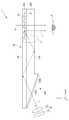
図1は、本実施形態の頭部装着型の表示装置1を説明する図である。図1は、使用状態の表示装置1を鉛直方向の上方から見た図である。
なお、以下の説明においては、理解を容易にするために、観察者が頭部に表示装置1を装着した状態における鉛直方向をZ方向とし、水平方向をX方向及びY方向とする。また、この水平方向のうち、導光板20に入光した映像光の導光方向(導光板20の左右方向)をX方向とし、それに直交する方向(導光板20の厚み方向)をY方向とする。また、Y方向のうち、−Y側を観察者側とし、+Y側を背面側とする。
FIG. 1 is a diagram illustrating a head-mounteddisplay device 1 of the present embodiment. FIG. 1 is a view of the usagestate display device 1 viewed from above in the vertical direction.
In the following description, in order to facilitate understanding, the vertical direction when the observer wears thedisplay device 1 on the head is the Z direction, and the horizontal direction is the X direction and the Y direction. Further, among these horizontal directions, the light guide direction (horizontal direction of the light guide plate 20) of the image light entering thelight guide plate 20 is the X direction, and the direction orthogonal to the light guide direction (thickness direction of the light guide plate 20) is the Y direction. To do. Further, in the Y direction, the −Y side is the observer side and the + Y side is the back side.

表示装置1は、観察者が頭部に装着し、観察者の眼前に映像を表示する、いわゆるヘッドマウントディスプレイである。本実施形態の表示装置1は、例えば、メガネフレーム(不図示)の内側に配置される。
表示装置1は、映像源10と、導光板20と、を備える。表示装置1は、観察者がメガネフレームを頭部に装着することによって、映像源10に表示された映像を、導光板20を介して観察者に視認させることができる。具体的には、表示装置1は、映像源10で形成された映像光Lを導光板20へ入光させ、導光板20内において+X方向に導光する。そして、表示装置1は、導光方向に直交する−Y方向に反射して、表示装置1を頭部に装着した観察者の眼Eの前に映像を表示する。
また、表示装置1は、導光板20に入光した外界から光の一部を観察者側に透過させて、映像と外界の光とを重ねて見せる、いわゆるシースルー機能を備えている。
Thedisplay device 1 is a so-called head-mounted display that the observer wears on the head and displays an image in front of the observer's eyes. Thedisplay device 1 of the present embodiment is arranged inside, for example, a spectacle frame (not shown).
Thedisplay device 1 includes avideo source 10 and alight guide plate 20. Thedisplay device 1 allows the observer to visually recognize the image displayed on theimage source 10 via thelight guide plate 20 by attaching the spectacle frame to the head of the observer. Specifically, thedisplay device 1 causes the image light L formed by theimage source 10 to enter thelight guide plate 20 and guides the light L in thelight guide plate 20 in the + X direction. Then, thedisplay device 1 reflects in the −Y direction orthogonal to the light guide direction, and displays an image in front of the eyes E of the observer wearing thedisplay device 1 on the head.
Further, thedisplay device 1 has a so-called see-through function in which a part of the light entering thelight guide plate 20 is transmitted to the observer side from the outside world to show the image and the light of the outside world in an overlapping manner.

映像源10は、ディスプレイ11と、投射光学系12と、を備える。
ディスプレイ11は、映像光を表示するマイクロディスプレイであり、例えば、透過型の液晶表示デバイス、反射型の液晶表示デバイス、有機EL等が使用される。具体的には、ディスプレイ11として、例えば、対角が1インチ以下のマイクロディスプレイが使用される。
投射光学系12は、映像源10から出射された映像光Lを導光板20に向けて投射する複数のレンズ群から構成される光学系である。図1では、投射光学系12を構成する複数のレンズ群を1枚のレンズとして模式的に図示している。
なお、図1では、映像源10から入光する映像光Lを1本の光線として図示しているが、映像光Lは、縦横に所定の大きさを有する画像として投射される。また、以下の説明においては、映像光L1、L2(後述)を総称して映像光Lともいう。
Theimage source 10 includes a display 11 and a projectionoptical system 12.
The display 11 is a microdisplay that displays video light, and for example, a transmissive liquid crystal display device, a reflective liquid crystal display device, an organic EL, or the like is used. Specifically, as the display 11, for example, a microdisplay having a diagonal of 1 inch or less is used.
The projectionoptical system 12 is an optical system composed of a plurality of lens groups that project the image light L emitted from theimage source 10 toward thelight guide plate 20. In FIG. 1, a plurality of lens groups constituting the projectionoptical system 12 are schematically shown as one lens.
In FIG. 1, the image light L entering from theimage source 10 is shown as one light ray, but the image light L is projected as an image having a predetermined size in the vertical and horizontal directions. Further, in the following description, the video light L1 and L2 (described later) are collectively referred to as the video light L.

導光板20は、光を導光する略平板状の透明な光学部材である。本実施形態の導光板20は、鉛直方向(Z方向)から見た形状が略台形形状に形成されている。導光板20は、第1導光層201と、第2導光層202と、を備える。第1導光層201は、第1全反射面121が形成された層である。第2導光層202は、入射面120及び第2全反射面122が形成された層である。以下、入射面120、第1全反射面121、第2全反射面122の順に説明する。 Thelight guide plate 20 is a substantially flat plate-shaped transparent optical member that guides light. Thelight guide plate 20 of the present embodiment is formed in a substantially trapezoidal shape when viewed from the vertical direction (Z direction). Thelight guide plate 20 includes a firstlight guide layer 201 and a secondlight guide layer 202. The firstlight guide layer 201 is a layer on which the firsttotal reflection surface 121 is formed. The secondlight guide layer 202 is a layer on which theincident surface 120 and the secondtotal reflection surface 122 are formed. Hereinafter, theincident surface 120, the firsttotal reflection surface 121, and the secondtotal reflection surface 122 will be described in this order.

入射面120は、映像光Lを第1全反射面121側に入射させる面である。入射面120は、導光板20の−X側の端部において、第1全反射面121に対して所定の角度で傾斜している。
入射面120は、入光した映像光Lを第1全反射面121において全反射させるために、第1全反射面121に対して25°〜30°の範囲で傾斜している。即ち、入射面120は、入光した映像光Lが、第1全反射面121において全反射する角度となるように、25°〜30°の範囲で形成されている。
Theincident surface 120 is a surface on which the image light L is incident on the firsttotal reflection surface 121 side. Theincident surface 120 is inclined at a predetermined angle with respect to the firsttotal reflection surface 121 at the end portion of thelight guide plate 20 on the −X side.
Theincident surface 120 is inclined in a range of 25 ° to 30 ° with respect to the firsttotal reflection surface 121 in order to totally reflect the incoming image light L on the firsttotal reflection surface 121. That is, theincident surface 120 is formed in a range of 25 ° to 30 ° so that the incoming image light L is totally reflected by the firsttotal reflection surface 121.

本実施形態の入射面120は、第1入射面120aと、第2入射面120bと、から構成される。
第1入射面120aは、導光板20において、第1全反射面121の−X側の端部と第2全反射面122の−X側の端部との間に形成されている。第1入射面120aは、入光した映像光Lを、第1全反射面121の垂線(不図示)に対して臨界角以上の角度で入射させる面である。ここで、第1全反射面121の垂線に対して臨界角以上の角度とは、第1全反射面121に入射した映像光Lが導光方向(X方向)に全反射する角度である。
Theincident surface 120 of the present embodiment is composed of afirst incident surface 120a and asecond incident surface 120b.
Thefirst incident surface 120a is formed between the end of the firsttotal reflection surface 121 on the −X side and the end of the secondtotal reflection surface 122 on the −X side in thelight guide plate 20. Thefirst incident surface 120a is a surface on which the incoming image light L is incident on the perpendicular line (not shown) of the firsttotal reflection surface 121 at an angle equal to or higher than the critical angle. Here, the angle equal to or greater than the critical angle with respect to the perpendicular line of the firsttotal reflection surface 121 is an angle at which the image light L incident on the firsttotal reflection surface 121 is totally reflected in the light guide direction (X direction).

第2入射面120bは、第2全反射面122よりも外側に位置している。具体的には、第2入射面120bは、第2全反射面122から観察者側(−Y側)に突出して形成されている。第2入射面120bは、入光した映像光Lの一部を、第1全反射面121の垂線(不図示)に対して臨界角以上の角度で入射させる面である。即ち、第1入射面120aが、入光した映像光Lのすべてを第1全反射面121に入射させるのに対して、第2入射面120bは、入光した映像光Lの一部を第1全反射面121に入射させる。
本実施形態の導光板20において、第1入射面120a及び第2入射面120bは、基材部26(後述)の−X側の端部において一体に形成され、第1全反射面121に対して同一の角度で傾斜している。
Thesecond incident surface 120b is located outside the secondtotal reflection surface 122. Specifically, thesecond incident surface 120b is formed so as to project from the secondtotal reflection surface 122 toward the observer side (−Y side). Thesecond incident surface 120b is a surface on which a part of the incoming image light L is incident on the perpendicular line (not shown) of the firsttotal reflection surface 121 at an angle equal to or higher than the critical angle. That is, thefirst incident surface 120a causes all of the incoming image light L to be incident on the firsttotal reflection surface 121, whereas thesecond incident surface 120b is a part of the incoming image light L. 1 It is incident on thetotal reflection surface 121.
In thelight guide plate 20 of the present embodiment, thefirst incident surface 120a and thesecond incident surface 120b are integrally formed at the −X side end portion of the base material portion 26 (described later) with respect to the firsttotal reflection surface 121. Are tilted at the same angle.

第1全反射面121は、導光板20を形成する面のうちXZ平面に平行であって、背面側(+Y側)に位置する面である。第1全反射面121は、入射面120から入射した映像光Lを第2全反射面122側に向けて全反射させる。
第2全反射面122は、導光板20を形成する面のうち、XZ平面に平行であって、観察者側(−Y側)に位置する面である。第2全反射面122と第1全反射面121は、導光板20の厚み方向(Y方向)において平行に形成されている。第2全反射面122は、第1全反射面121において全反射した映像光Lを、第1全反射面121側に向けて全反射させる。また、第2全反射面122は、+X側の端部が、単位光学形状部30及び出光側単位光学形状部31(後述)において反射した映像光Lを導光板20外へ出光する出光面となる。
The firsttotal reflection surface 121 is a surface of the surfaces forming thelight guide plate 20 that is parallel to the XZ plane and is located on the back surface side (+ Y side). The firsttotal reflection surface 121 totally reflects the image light L incident from theincident surface 120 toward the secondtotal reflection surface 122.
The secondtotal reflection surface 122 is a surface of the surfaces forming thelight guide plate 20 that is parallel to the XZ plane and is located on the observer side (−Y side). The secondtotal reflection surface 122 and the firsttotal reflection surface 121 are formed in parallel in the thickness direction (Y direction) of thelight guide plate 20. The secondtotal reflection surface 122 totally reflects the image light L totally reflected by the firsttotal reflection surface 121 toward the firsttotal reflection surface 121 side. Further, in the secondtotal reflection surface 122, the end portion on the + X side is a light emitting surface that emits the image light L reflected by the unitoptical shape portion 30 and the light emitting side unit optical shape portion 31 (described later) to the outside of thelight guide plate 20. Become.

上記構成において、入射面120から導光板20に入光された映像光Lは、第1全反射面121で全反射する角度となるように導光される。第1全反射面121及び第2全反射面122は、導光板20の厚み方向(Y方向)において平行であるため、映像光Lは、第1全反射面121及び第2全反射面122の間で全反射を繰り返しながら、導光板20内の+X方向(導光方向)に導光される。なお、導光板20に入光した映像光Lの光路については、後述する。 In the above configuration, the image light L that enters thelight guide plate 20 from theincident surface 120 is guided so as to have an angle that is totally reflected by the firsttotal reflection surface 121. Since the firsttotal reflection surface 121 and the secondtotal reflection surface 122 are parallel in the thickness direction (Y direction) of thelight guide plate 20, the image light L is the image light L of the firsttotal reflection surface 121 and the secondtotal reflection surface 122. The light is guided in the + X direction (light guide direction) in thelight guide plate 20 while repeating total reflection between them. The optical path of the image light L that has entered thelight guide plate 20 will be described later.

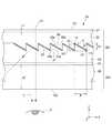
次に、導光板20の層構成について説明する。
図2は、本実施形態の導光板20の詳細を説明する図である。図2は、図1のa部の詳細を示している。
図2に示すように、導光板20は、観察者側(−Y側)から順に、基材部26、接合層24、第2光学形状層23、第1光学形状層22及び基材部21が積層されている。
Next, the layer structure of thelight guide plate 20 will be described.
FIG. 2 is a diagram illustrating details of thelight guide plate 20 of the present embodiment. FIG. 2 shows the details of part a in FIG.
As shown in FIG. 2, thelight guide plate 20 has abase material portion 26, abonding layer 24, a secondoptical shape layer 23, a firstoptical shape layer 22, and abase material portion 21 in this order from the observer side (−Y side). Are laminated.

基材部21及び基材部26は、導光板20の基礎となる平板状の部材であり、例えば、光透過性の高いアクリル樹脂、スチレン樹脂、アクリルスチレン樹脂、ポリカーボネート樹脂、脂環式ポリオレフィン樹脂等から形成されている。
基材部21は、導光板20の最も背面側に設けられた層であり、その背面側(+Y側)の面が第1全反射面121となる。基材部21は、第1光学形状層22の基礎となる基材であり、その厚みs1は、後述する単位光学形状部30の深さd1及びd2に合わせて、10μm≦s1≦100μmの範囲で形成されることが望ましい。基材部21の背面側の面は、入射する光の拡散を抑制する観点から平滑(例えば、60度の光沢度で90以上)に形成されるのが望ましい。
Thebase material portion 21 and thebase material portion 26 are flat plate-shaped members that form the basis of thelight guide plate 20, and are, for example, highly light-transmitting acrylic resin, styrene resin, acrylic styrene resin, polycarbonate resin, and alicyclic polyolefin resin. Etc. are formed from.
Thebase material portion 21 is a layer provided on the innermost back side of thelight guide plate 20, and the surface on the back surface side (+ Y side) thereof is the firsttotal reflection surface 121. Thebase material portion 21 is a base material that is the basis of the firstoptical shape layer 22, and the thickness s1 thereof is in the range of 10 μm ≦ s1 ≦ 100 μm according to the depths d1 and d2 of the unitoptical shape part 30 described later. It is desirable to be formed with. The surface on the back surface side of thebase material portion 21 is preferably formed to be smooth (for example, 90 or more at a glossiness of 60 degrees) from the viewpoint of suppressing the diffusion of incident light.

基材部26は、導光板20の最も観察者側に設けられた層であり、その観察者側(−Y側)の面が、第2全反射面122となる。基材部26は、第2光学形状層23の背面側に接合層24を介して接合される。基材部26は、導光板20の全体の厚みを調整するとともに、導光板20に所定の剛性を持たせる基材である。また、基材部26の−X側の端部には、入射面120(図1参照)が形成される。 Thebase material portion 26 is a layer provided on the most observer side of thelight guide plate 20, and the surface on the observer side (−Y side) is the secondtotal reflection surface 122. Thebase material portion 26 is bonded to the back surface side of the secondoptical shape layer 23 via thebonding layer 24. Thebase material portion 26 is a base material that adjusts the overall thickness of thelight guide plate 20 and gives the light guide plate 20 a predetermined rigidity. Further, an incident surface 120 (see FIG. 1) is formed at the end portion of thebase material portion 26 on the −X side.

基材部26の厚みs2は、2mm≦s2≦3mmの範囲で形成されることが好ましい。厚みs2が2mm未満である場合、導光板20の剛性が低下したり、導光板20の出光面に表示される画面が小さくなりすぎたりするため望ましくない。また、厚みs2が3mmを超える場合、導光板20の重量が増し、表示装置1を装着する観察者の負荷となるため望ましくない。
基材部26の観察者側の面は、光の拡散を抑制する観点から平滑(例えば、60度の光沢度で90以上)に形成されるのが望ましい。
The thickness s2 of thebase material portion 26 is preferably formed in the range of 2 mm ≦ s2 ≦ 3 mm. If the thickness s2 is less than 2 mm, the rigidity of thelight guide plate 20 is lowered, and the screen displayed on the light emitting surface of thelight guide plate 20 becomes too small, which is not desirable. Further, when the thickness s2 exceeds 3 mm, the weight of thelight guide plate 20 increases, which is not desirable because it imposes a load on the observer who wears thedisplay device 1.
The surface of thebase material portion 26 on the observer side is preferably formed to be smooth (for example, 90 or more at a glossiness of 60 degrees) from the viewpoint of suppressing the diffusion of light.

第1光学形状層22は、基材部21の観察者側(−Y側)の面に設けられる層である。第1光学形状層22としては、光透過性の高いウレタンアクリレート系、ポリエステルアクリレート系、エポキシアクリレート系、ポリエーテルアクリレート系、ポリチオール系、ブタジエンアクリレート系等の紫外線硬化樹脂が用いられる。第1光学形状層22の屈折率は、上述の基材部21、基材部26と同等の屈折率であることが望ましい。なお、本実施形態では、導光板20を形成する樹脂として、紫外線硬化樹脂を例に挙げて説明するが、これに限定されない。導光板20を形成する樹脂は、例えば、電子線硬化樹脂であってもよい。 The firstoptical shape layer 22 is a layer provided on the surface of thebase material portion 21 on the observer side (−Y side). As the firstoptical shape layer 22, an ultraviolet curable resin such as urethane acrylate-based, polyester acrylate-based, epoxy acrylate-based, polyether acrylate-based, polythiol-based, or butadiene acrylate-based, which has high light transmittance, is used. It is desirable that the refractive index of the firstoptical shape layer 22 is the same as that of thebase material portion 21 and thebase material portion 26 described above. In the present embodiment, the ultraviolet curable resin will be described as an example of the resin forming thelight guide plate 20, but the present invention is not limited to this. The resin forming thelight guide plate 20 may be, for example, an electron beam curing resin.

第1光学形状層22は、図1及び図2に示すように、その観察者側(−Y側)の面であって、+X側の端部近傍に、単位光学形状部30が複数設けられている。
単位光学形状部30は、鉛直方向(Z方向)に延在し、映像光Lの導光方向(X方向)に沿って複数配列されている。また、単位光学形状部30は、映像光Lが出光する方向(導光板20の厚み方向、Y方向)に平行、且つ、単位光学形状部30の配列方向(X方向)に平行な断面(XY面)における形状が三角形状(プリズム形状)に形成されている。単位光学形状部30は、第1傾斜面30aと、第2傾斜面30bと、から構成される。
As shown in FIGS. 1 and 2, the firstoptical shape layer 22 is a surface on the observer side (−Y side), and a plurality of unitoptical shape portions 30 are provided near the end portion on the + X side. ing.
A plurality of unitoptical shape portions 30 extend in the vertical direction (Z direction) and are arranged along the light guide direction (X direction) of the image light L. Further, the unitoptical shape portion 30 has a cross section (XY) parallel to the direction in which the image light L is emitted (thickness direction of thelight guide plate 20, Y direction) and parallel to the arrangement direction (X direction) of the unitoptical shape portion 30. The shape on the surface) is formed in a triangular shape (prism shape). The unitoptical shape portion 30 is composed of a firstinclined surface 30a and a secondinclined surface 30b.

第1傾斜面30aは、第2全反射面122で全反射した映像光Lが直接入射する面である。第1傾斜面30aは、出光面(第2全反射面122、第2光学形状層23の観察者側の面)に対して傾斜しており、その+X側の端部が、−X側の端部よりも観察者(出光)側(−Y側)に位置している。
また、第1傾斜面30a上の全面、即ち、第1傾斜面30a及び第3傾斜面31a(後述)間の全体には、反射層25が形成されている。
The firstinclined surface 30a is a surface on which the image light L totally reflected by the secondtotal reflection surface 122 is directly incident. The firstinclined surface 30a is inclined with respect to the light emitting surface (the secondtotal reflection surface 122, the surface of the secondoptical shape layer 23 on the observer side), and the end portion on the + X side thereof is on the −X side. It is located on the observer (Idemitsu) side (-Y side) from the end.
Further, areflective layer 25 is formed on the entire surface of the firstinclined surface 30a, that is, the entire area between the firstinclined surface 30a and the thirdinclined surface 31a (described later).

第2傾斜面30bは、第2全反射面122で全反射した映像光Lが直接入射しない面である。第2傾斜面30bは、第1傾斜面30aよりも映像光Lの進行する側(+X側)に、第1傾斜面30aと対向して設けられている。第2傾斜面30bは、出光面(第2全反射面122、第2光学形状層23の観察者側の面)に対して傾斜しており、その+X側の端部が、−X側の端部よりも背面側(+Y側)に位置している。 The secondinclined surface 30b is a surface on which the image light L totally reflected by the secondtotal reflection surface 122 is not directly incident. The secondinclined surface 30b is provided on the side (+ X side) where the image light L travels with respect to the firstinclined surface 30a, facing the firstinclined surface 30a. The secondinclined surface 30b is inclined with respect to the light emitting surface (the secondtotal reflection surface 122, the surface of the secondoptical shape layer 23 on the observer side), and the end portion on the + X side thereof is on the −X side. It is located on the back side (+ Y side) of the end.

第2光学形状層23は、第1光学形状層22の単位光学形状部30側(観察者側)の面に設けられた層である。第2光学形状層23は、第1光学形状層22の観察者側(−Y側)の面を平坦にするために設けられている。第2光学形状層23としては、先に説明した第1光学形状層22と同じ紫外線硬化樹脂が用いられる。第2光学形状層23の屈折率は、第1光学形状層22と同等であることが望ましい。 The secondoptical shape layer 23 is a layer provided on the surface of the firstoptical shape layer 22 on the unitoptical shape portion 30 side (observer side). The secondoptical shape layer 23 is provided to flatten the surface of the firstoptical shape layer 22 on the observer side (−Y side). As the secondoptical shape layer 23, the same ultraviolet curable resin as the firstoptical shape layer 22 described above is used. It is desirable that the refractive index of the secondoptical shape layer 23 is the same as that of the firstoptical shape layer 22.

第2光学形状層23の観察者側の面は、接合層24を介して基材部26に接合される面である。また、この面は、第2光学形状層23から基材部26へ通過する光の出光面となる。第2光学形状層23の出光面は、導光板20の第2全反射面122(出光面、XZ平面)と平行である。
第2光学形状層23は、第1光学形状層22と対向する面(背面、+Y側の面)に上述の単位光学形状部30と対応する形状の出光側単位光学形状部31が形成されている。
The surface of the secondoptical shape layer 23 on the observer side is a surface bonded to thebase material portion 26 via thebonding layer 24. Further, this surface serves as an emission surface of light passing from the secondoptical shape layer 23 to thebase material portion 26. The light emitting surface of the secondoptical shape layer 23 is parallel to the second total reflection surface 122 (light emitting surface, XZ plane) of thelight guide plate 20.
In the secondoptical shape layer 23, an demitsu side unitoptical shape portion 31 having a shape corresponding to the above-mentioned unitoptical shape portion 30 is formed on a surface (rear surface, + Y side surface) facing the firstoptical shape layer 22. There is.

出光側単位光学形状部31は、鉛直方向(Z方向)に延在し、映像光Lの導光方向(X方向)に沿って複数配列されている。出光側単位光学形状部31は、映像光Lが出光する方向(導光板20の厚み方向、Y方向)に平行、且つ、出光側単位光学形状部31の配列方向(X方向)に平行な断面(XY面)における形状が三角形状(プリズム形状)に形成されている。出光側単位光学形状部31は、第3傾斜面31aと、第4傾斜面31bと、から構成される。
本実施形態において、出光側単位光学形状部31及び単位光学形状部30は、上記断面において、同様の形状に形成されている。
A plurality of unitoptical shape portions 31 on the light emitting side extend in the vertical direction (Z direction) and are arranged along the light guide direction (X direction) of the image light L. The light emitting side unitoptical shape portion 31 has a cross section parallel to the direction in which the image light L is emitted (thickness direction of thelight guide plate 20, Y direction) and parallel to the arrangement direction (X direction) of the light emitting side unitoptical shape portion 31. The shape on the (XY plane) is formed into a triangular shape (prism shape). The light emitting side unitoptical shape portion 31 is composed of a thirdinclined surface 31a and a fourthinclined surface 31b.
In the present embodiment, the light emitting side unitoptical shape portion 31 and the unitoptical shape portion 30 are formed in the same shape in the above cross section.

第3傾斜面31aは、第2全反射面122で全反射した映像光Lが直接入射する面である。第3傾斜面31aは、出光面(第2全反射面122、第2光学形状層23の観察者側の面)に対して傾斜しており、その+X側の端部が、−X側の端部よりも観察者(出光)側(−Y側)に位置している。第3傾斜面31aは、単位光学形状部30の第1傾斜面30aに対向しており、その第1傾斜面30aと平行な面である。上述したように、第3傾斜面31a及び第1傾斜面30a間には、反射層25が設けられている。 The thirdinclined surface 31a is a surface on which the image light L totally reflected by the secondtotal reflection surface 122 is directly incident. The thirdinclined surface 31a is inclined with respect to the light emitting surface (the secondtotal reflection surface 122, the surface of the secondoptical shape layer 23 on the observer side), and the end portion on the + X side thereof is on the −X side. It is located on the observer (Idemitsu) side (-Y side) from the end. The thirdinclined surface 31a is a surface that faces the firstinclined surface 30a of the unitoptical shape portion 30 and is parallel to the firstinclined surface 30a. As described above, thereflective layer 25 is provided between the thirdinclined surface 31a and the firstinclined surface 30a.

第4傾斜面31bは、第2全反射面122で全反射した映像光Lが直接入射しない面である。第4傾斜面31bは、第3傾斜面31aよりも映像源側(−X側)に、第3傾斜面と対向して設けられている。第4傾斜面31bは、出光面(第2全反射面122、第2光学形状層23の観察者側の面)に対して傾斜しており、その+X側の端部が、−X側の端部よりも背面側(+Y側)に位置している。第4傾斜面31bは、単位光学形状部30の第2傾斜面30bに対向しており、第2傾斜面30bと平行な面である。第4傾斜面31bは、上述した第2傾斜面30bに密着している。 The fourthinclined surface 31b is a surface on which the image light L totally reflected by the secondtotal reflection surface 122 is not directly incident. The fourthinclined surface 31b is provided on the image source side (-X side) of the thirdinclined surface 31a so as to face the third inclined surface. The fourthinclined surface 31b is inclined with respect to the light emitting surface (the secondtotal reflection surface 122, the surface of the secondoptical shape layer 23 on the observer side), and the end portion on the + X side thereof is on the −X side. It is located on the back side (+ Y side) of the end. The fourthinclined surface 31b is a surface that faces the secondinclined surface 30b of the unitoptical shape portion 30 and is parallel to the secondinclined surface 30b. The fourthinclined surface 31b is in close contact with the above-mentioned secondinclined surface 30b.

ここで、第1傾斜面30a及び第3傾斜面31aが、第1全反射面121(出光面)に平行な面(XZ平面)と交差する角度は、αである。第2傾斜面30b及び第4傾斜面31bが、第2全反射面122(出光面)に平行な面(XZ平面)と交差する角度は、βである。単位光学形状部30及び出光側単位光学形状部31の配列ピッチは、Pである。単位光学形状部30の高さ(導光板20の厚み方向(Y方向)における単位光学形状部30の頂部t1から単位光学形状部30間の谷部v1までの寸法)は、h1である。出光側単位光学形状部31の高さ(導光板20の厚み方向(Y方向)における出光側単位光学形状部31の頂部t2から出光側単位光学形状部31間の谷部v2までの寸法)は、h2である。本実施形態において、h1=h2である。 Here, the angle at which the firstinclined surface 30a and the thirdinclined surface 31a intersect with the surface (XZ plane) parallel to the first total reflection surface 121 (light emitting surface) is α. The angle at which the secondinclined surface 30b and the fourthinclined surface 31b intersect the surface (XZ plane) parallel to the second total reflection surface 122 (light emitting surface) is β. The arrangement pitch of the unitoptical shape portion 30 and the unitoptical shape portion 31 on the light emitting side is P. The height of the unit optical shape portion 30 (the dimension from the top t1 of the unitoptical shape portion 30 in the thickness direction (Y direction) of thelight guide plate 20 to the valley portion v1 between the unit optical shape portions 30) is h1. The height of the light emitting side unit optical shape portion 31 (the dimension from the top t2 of the light emitting side unitoptical shape portion 31 in the thickness direction (Y direction) of thelight guide plate 20 to the valley v2 between the light emitting side unit optical shape portions 31) is , H2. In this embodiment, h1 = h2.

なお、本実施形態では、配列ピッチPが第1傾斜面30a及び第3傾斜面31aの配列方向(X方向)における幅寸法と同等である例について説明するが、これに限らず、各傾斜面の幅寸法よりも大きくなるようにしてもよい。 In this embodiment, an example in which the arrangement pitch P is equivalent to the width dimension of the firstinclined surface 30a and the thirdinclined surface 31a in the arrangement direction (X direction) will be described, but the present invention is not limited to this, and each inclined surface is not limited to this. It may be larger than the width dimension of.

本実施形態の単位光学形状部30及び出光側単位光学形状部31は、配列ピッチP等が一定で、角度αが映像光Lの進行する側(+X側)へ向かうにつれて次第に大きくなり、また、それに伴い高さh1、h2も大きくなる例について説明するが、これに限定されない。例えば、配列ピッチP、角度α、角度β、高さh1、h2が一定に形成されるようにしてもよい。 In the unitoptical shape portion 30 and the light emitting side unitoptical shape portion 31 of the present embodiment, the array pitch P and the like are constant, and the angle α gradually increases toward the traveling side (+ X side) of the image light L, and further. An example in which the heights h1 and h2 increase accordingly will be described, but the present invention is not limited to this. For example, the array pitch P, the angle α, the angle β, and the heights h1 and h2 may be formed to be constant.

接合層24は、基材部26及び第2光学形状層23を接合する粘着剤である。接合層24は、基材部26及び第2光学形状層23間を透過する映像光Lが屈折しないような材料であることが好ましい。そのため、上述した層と同等の屈折率を有する材料、例えば、光透過性の高いウレタンアクリレート樹脂、エポキシアクリレート樹脂、アクリル系粘着剤、シリコン系粘着剤等により形成されている。 Thebonding layer 24 is an adhesive that bonds thebase material portion 26 and the secondoptical shape layer 23. Thebonding layer 24 is preferably made of a material such that the image light L transmitted between thebase material portion 26 and the secondoptical shape layer 23 is not refracted. Therefore, it is formed of a material having a refractive index equivalent to that of the above-mentioned layer, for example, a urethane acrylate resin having high light transmittance, an epoxy acrylate resin, an acrylic pressure-sensitive adhesive, a silicon-based pressure-sensitive adhesive, or the like.

反射層25は、入射した光の一部を反射し、その他を透過する半透過型の反射層、いわゆるハーフミラーである。反射層25の反射率と透過率の割合は、適宜に設定できるが、映像光Lを良好に反射させるとともに、外界の光を良好に透過させる観点から、透過率が40〜60%の範囲であることが望ましい。本実施形態の反射層25は、反射率及び透過率がともに50%のハーフミラー状に形成されている。 Thereflective layer 25 is a semi-transmissive reflective layer, a so-called half mirror, that reflects a part of the incident light and transmits the other. The ratio of the reflectance and the transmittance of thereflective layer 25 can be appropriately set, but the transmittance is in the range of 40 to 60% from the viewpoint of satisfactorily reflecting the image light L and satisfactorily transmitting the light of the outside world. It is desirable to have. Thereflective layer 25 of the present embodiment is formed in a half mirror shape having both reflectance and transmittance of 50%.

反射層25は、第1傾斜面30aの面上、即ち第1傾斜面30a及び第3傾斜面31a間に光反射性の高い金属、例えば、アルミニウム、銀、ニッケル等により形成されている。本実施形態において、反射層25は、アルミニウムを蒸着することにより形成されている。また、これに限らず反射層25は、光反射性の高い金属をスパッタリングしたり、金属箔を転写したり、金属薄膜を含有した塗料を塗布したりする等により形成されてもよい。また、反射層25として、酸化チタン、酸化シリコン、ニオブ、タンタル、フッ化マグネシウム等を複数積層した誘電体多層膜を形成してもよい。誘電体多層膜は、屈折率の高い誘電体膜と屈折率の低い誘電体膜とを交互に積層した膜である。
本実施形態の反射層25は、アルミニウムの蒸着によって約100Åの厚みに形成されているが、光の反射率及び透過率を上述の好ましい範囲に設定できれば、その材料等に応じて厚さを自由に設定できる。
Thereflective layer 25 is formed of a metal having high light reflectivity, for example, aluminum, silver, nickel, etc., on the surface of the firstinclined surface 30a, that is, between the firstinclined surface 30a and the thirdinclined surface 31a. In this embodiment, thereflective layer 25 is formed by depositing aluminum. Further, thereflective layer 25 is not limited to this, and may be formed by sputtering a metal having high light reflectivity, transferring a metal foil, applying a paint containing a metal thin film, or the like. Further, as thereflective layer 25, a dielectric multilayer film in which a plurality of titanium oxide, silicon oxide, niobium, tantalum, magnesium fluoride and the like are laminated may be formed. The dielectric multilayer film is a film in which a dielectric film having a high refractive index and a dielectric film having a low refractive index are alternately laminated.
Thereflective layer 25 of the present embodiment is formed to have a thickness of about 100 Å by vapor deposition of aluminum, but if the reflectance and transmittance of light can be set within the above-mentioned preferable ranges, the thickness can be freely adjusted according to the material and the like. Can be set to.

ここで、単位光学形状部30及び出光側単位光学形状部31において、映像光Lを効率良く反射して導光板20から出光させるためのパラメータについて例示する。
単位光学形状部30において、第1傾斜面30a及び第3傾斜面31aの角度αは、25°≦α≦40°の範囲に形成されることが望ましい。
出光側単位光学形状部31において、第2傾斜面30b及び第4傾斜面31bの角度βは、80°≦β≦90°の範囲に形成されることが望ましい。
単位光学形状部30の高さh1及び出光側単位光学形状部31の高さh2は、それぞれ、20μm≦h1≦700μm、20μm≦h2≦700μmの範囲に形成することが望ましい。
単位光学形状部30の配列ピッチPは、50μm≦P≦1000μmの範囲で形成することが望ましい。
Here, the parameters for efficiently reflecting the image light L and emitting light from thelight guide plate 20 in the unitoptical shape unit 30 and the light emitting side unitoptical shape unit 31 will be illustrated.
In the unitoptical shape portion 30, it is desirable that the angle α of the firstinclined surface 30a and the thirdinclined surface 31a is formed in the range of 25 ° ≦ α ≦ 40 °.
In the light emitting side unitoptical shape portion 31, it is desirable that the angle β of the secondinclined surface 30b and the fourthinclined surface 31b is formed in the range of 80 ° ≦ β ≦ 90 °.
It is desirable that the height h1 of the unitoptical shape portion 30 and the height h2 of the unitoptical shape portion 31 on the light emitting side are formed in the ranges of 20 μm ≦ h1 ≦ 700 μm and 20 μm ≦ h2 ≦ 700 μm, respectively.
It is desirable that the array pitch P of the unitoptical shape portion 30 is formed in the range of 50 μm ≦ P ≦ 1000 μm.

次に、本実施形態の導光板20から出光する映像光L及び外界の光Gの光路について説明する。
図1に示すように、映像源10から投射された映像光Lは、投射光学系12を介して導光板20の入射面120へ入光する。導光板20内に入光した映像光Lは、入射面120と空気との境界面で屈折し、第1全反射面121へ入射する。その映像光Lは、第1全反射面121において第2全反射面122側へ全反射した後、第2全反射面122に入射して単位光学形状部30側へ全反射する。このように、映像光Lは、第1全反射面121及び第2全反射面122間において全反射を繰り返すことにより、導光板20の−X側から+X側に向けて導光され、第1光学形状層22及び第2光学形状層23間に設けられた反射層25に入射する。
Next, the optical paths of the image light L and the light G in the outside world emitted from thelight guide plate 20 of the present embodiment will be described.
As shown in FIG. 1, the image light L projected from theimage source 10 enters theincident surface 120 of thelight guide plate 20 via the projectionoptical system 12. The image light L that has entered thelight guide plate 20 is refracted at the interface between theincident surface 120 and the air, and is incident on the firsttotal reflection surface 121. The image light L is totally reflected on the firsttotal reflection surface 121 toward the secondtotal reflection surface 122, then incident on the secondtotal reflection surface 122 and totally reflected toward the unitoptical shape portion 30 side. In this way, the image light L is guided from the −X side to the + X side of thelight guide plate 20 by repeating total reflection between the firsttotal reflection surface 121 and the secondtotal reflection surface 122, and the first It is incident on thereflection layer 25 provided between theoptical shape layer 22 and the secondoptical shape layer 23.

なお、図1では、説明を容易にするため、映像光Lが第1全反射面121及び第2全反射面122においてそれぞれ1回全反射する例を示している。これに限らず、映像光Lが各面でより多く全反射を繰り返す構成であってもよい。 Note that FIG. 1 shows an example in which the image light L is totally reflected once on each of the firsttotal reflection surface 121 and the secondtotal reflection surface 122 for the sake of simplicity. Not limited to this, the image light L may be configured to repeat total reflection more on each surface.

反射層25に入射した映像光のうち、一部の映像光Lは、図2に示すように、反射層25において第1全反射面121に対してほぼ垂直な方向(−Y方向)に反射して、第2全反射面122から観察者の眼Eに向けて出光する。また、他の映像光は、反射層25を透過して第1光学形状層22内に入射するが、そのほとんどが導光板20の背面側から出光する。 Of the image light incident on thereflection layer 25, a part of the image light L is reflected by thereflection layer 25 in a direction (−Y direction) substantially perpendicular to the firsttotal reflection surface 121, as shown in FIG. Then, light is emitted from the secondtotal reflection surface 122 toward the observer's eye E. Further, other video light passes through thereflection layer 25 and enters the firstoptical shape layer 22, but most of the light is emitted from the back surface side of thelight guide plate 20.

外界の光Gは、図1に示すように、導光板20の背面側(+Y側)の第1全反射面121から導光板20内に入光する。導光板20内に入光した外界の光Gのうち一部の光は、反射層25に入射する。その一部の光G1は、図2に示すように、反射層25を透過して、第2全反射面122(出光面)から観察者の眼Eに向けて出光する。また、他の光は、反射層25と第1光学形状層22との界面で背面側(+Y側)に反射する。 As shown in FIG. 1, the light G in the outside world enters thelight guide plate 20 from the firsttotal reflection surface 121 on the back surface side (+ Y side) of thelight guide plate 20. A part of the light G in the outside world that has entered thelight guide plate 20 is incident on thereflection layer 25. As shown in FIG. 2, a part of the light G1 passes through thereflection layer 25 and emits light from the second total reflection surface 122 (emission surface) toward the observer's eye E. Further, other light is reflected to the back surface side (+ Y side) at the interface between thereflection layer 25 and the firstoptical shape layer 22.

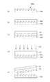
次に、本実施形態の導光板20の製造方法について説明する。
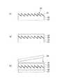
図3及び図4は、本実施形態の導光板20の製造方法を説明する図である。このうち、図3の各分図(a)〜(e)は、基材部21と接合された第1光学形状層22を製造する過程を説明する図である。また、図4の各分図(f)〜(h)は、基材部21と接合された第1光学形状層22を基にして導光板20を製造する過程を説明する図である。なお、図3及び図4では、部材の断面を示すハッチングを適宜に省略する。
Next, a method of manufacturing thelight guide plate 20 of the present embodiment will be described.
3 and 4 are views for explaining the method of manufacturing thelight guide plate 20 of the present embodiment. Of these, the respective fractions (a) to (e) of FIG. 3 are views for explaining the process of manufacturing the firstoptical shape layer 22 bonded to thebase material portion 21. Further, FIGS. 4F to 4H are views for explaining a process of manufacturing thelight guide plate 20 based on the firstoptical shape layer 22 joined to thebase material portion 21. In addition, in FIG. 3 and FIG. 4, hatching showing a cross section of a member is appropriately omitted.

まず、図3(a)に示すように、製造する導光板20の第1光学形状層22の形状に対応した賦形面100aを有する成形型100を用意し、賦形面100aが上方(重力方向の天側)を向くように配置する。成形型100は、金型でもよいし、樹脂型でもよい。
次に、図3(b)に示すように、賦形面100a上に紫外線硬化樹脂22aを均一に形成する。ここでは、例えば、紫外線硬化樹脂22aを、賦形面100a上の一辺に沿って点状又は線状に塗布し、ローラ等(不図示)で引き延ばすことにより、賦形面100a上に均一に形成することができる。
First, as shown in FIG. 3A, amolding die 100 having a shapingsurface 100a corresponding to the shape of the firstoptical shape layer 22 of thelight guide plate 20 to be manufactured is prepared, and theshaping surface 100a is upward (gravity). Place it so that it faces the top side of the direction. The molding die 100 may be a mold or a resin mold.
Next, as shown in FIG. 3B, the ultravioletcurable resin 22a is uniformly formed on theshaping surface 100a. Here, for example, the ultravioletcurable resin 22a is applied in a dot shape or a linear shape along one side on theshaping surface 100a and stretched by a roller or the like (not shown) to be uniformly formed on theshaping surface 100a. can do.

次に、図3(c)に示すように、賦形面100a上に塗布された紫外線硬化樹脂22aの上に、基材部21を貼り付ける。
次に、図3(d)に示すように、紫外線照射部(不図示)から、未硬化の紫外線硬化樹脂22aに対して紫外線UVを照射する。これにより、紫外線硬化樹脂22aが硬化して第1光学形状層22となる。本実施形態において、紫外線UVは、基材部21を介して紫外線硬化樹脂22aに照射される。
紫外線硬化樹脂22aが硬化した後、図3(e)に示すように、第1光学形状層22を成形型100から剥離することにより、基材部21と接合された第1光学形状層22を得ることができる。
Next, as shown in FIG. 3C, thebase material portion 21 is attached onto the ultravioletcurable resin 22a coated on theshaping surface 100a.
Next, as shown in FIG. 3D, the uncured ultravioletcurable resin 22a is irradiated with ultraviolet UV from the ultraviolet irradiation unit (not shown). As a result, the ultravioletcurable resin 22a is cured to form the firstoptical shape layer 22. In the present embodiment, the ultraviolet UV is applied to the ultravioletcurable resin 22a via thebase material portion 21.
After the ultravioletcurable resin 22a is cured, as shown in FIG. 3E, the firstoptical shape layer 22 is peeled from the molding die 100 to form the firstoptical shape layer 22 bonded to thebase material portion 21. Obtainable.

次に、図4(f)に示すように、単位光学形状部30の表面に蒸着金属を付着させて、反射層25を形成する。なお、この工程では、第1光学形状層22の単位光学形状部30が下方を向くように配置して、単位光学形状部30の表面に蒸着金属を付着させる。 Next, as shown in FIG. 4 (f), the vapor-deposited metal is adhered to the surface of the unitoptical shape portion 30 to form thereflective layer 25. In this step, the unitoptical shape portion 30 of the firstoptical shape layer 22 is arranged so as to face downward, and the vapor-deposited metal is adhered to the surface of the unitoptical shape portion 30.

また、図4(f)では、第1光学形状層22のすべての領域に反射層25が形成されているが、反射層25は、映像光の出光側となる領域のみに形成され、映像光が導光される領域には形成されない。反射層25が形成されない領域は、第2光学形状層23(後述)と直接に接合される。映像光の出光側となる領域のみに反射層25を形成するには、反射層25を形成する領域と同じ大きさの開口を有するステンシルマスク(不図示)を、第1光学形状層22を覆うように配置して、蒸着金属をマスキング蒸着すればよい。 Further, in FIG. 4 (f), thereflective layer 25 is formed in all the regions of the firstoptical shape layer 22, but thereflective layer 25 is formed only in the region on the light emitting side of the image light, and the image light is formed. Is not formed in the region where the light is guided. The region where thereflective layer 25 is not formed is directly joined to the second optical shape layer 23 (described later). In order to form thereflective layer 25 only in the region on the light emitting side of the image light, a stencil mask (not shown) having an opening having the same size as the region forming thereflective layer 25 covers the firstoptical shape layer 22. The vapor-deposited metal may be masked and vapor-deposited.

次に、図4(g)に示すように、第1光学形状層22の単位光学形状部30が設けられた側の面に、第2光学形状層23を形成する。ここでは、例えば、紫外線硬化樹脂を、第1光学形状層22の一辺に沿って点状又は線状に塗布し、ローラ等(不図示)で引き延ばすことにより、均一に形成できる。図示を省略するが、この後、第1光学形状層22上に形成した紫外線硬化樹脂に対して紫外線を照射することにより、紫外線硬化樹脂が硬化して第2光学形状層23となる。 Next, as shown in FIG. 4 (g), the secondoptical shape layer 23 is formed on the surface of the firstoptical shape layer 22 on the side where the unitoptical shape portion 30 is provided. Here, for example, the ultraviolet curable resin can be uniformly formed by applying it in a dot shape or a linear shape along one side of the firstoptical shape layer 22 and stretching it with a roller or the like (not shown). Although not shown, the ultraviolet curable resin is cured by irradiating the ultraviolet curable resin formed on the firstoptical shape layer 22 with ultraviolet rays to form the secondoptical shape layer 23.

次に、図4(h)に示すように、第2光学形状層23側の面に接合層24を形成して、基材部26を貼り付ける。
そして、接合層24を介して基材部26が貼付された積層体の−X側(単位光学形状部30が形成される側とは反対側)の観察者側(−Y側)の角部を加工して入射面120を形成する。以上の工程を経ることにより、導光板20が完成する。
Next, as shown in FIG. 4H, abonding layer 24 is formed on the surface of the secondoptical shape layer 23 side, and thebase material portion 26 is attached.
Then, the corner portion on the observer side (-Y side) on the −X side (the side opposite to the side on which the unitoptical shape portion 30 is formed) of the laminate to which thebase material portion 26 is attached via thebonding layer 24. Is processed to form theincident surface 120. By going through the above steps, thelight guide plate 20 is completed.

次に、本実施形態の導光板20及び比較例の導光板20Cにおける映像光の入光範囲について説明する。
図5は、導光板における映像光Lの入光範囲を説明する図である。図5(a)は、比較例の導光板20Cにおける映像光Lの入光範囲を説明する図である。図5(b)は、本実施形態の導光板20における映像光Lの入光範囲を説明する図である。なお、図5(a)では、上述した実施形態(図1)と同じ構成要素に同一符号を付し、その符号に続いて「c」を付している。また、図5に示す各図では、説明に必要な部分にのみ符号を付している。
Next, the light input range of the image light in thelight guide plate 20 of the present embodiment and the light guide plate 20C of the comparative example will be described.
FIG. 5 is a diagram illustrating an incoming light range of the image light L in the light guide plate. FIG. 5A is a diagram illustrating an incoming light range of the image light L in the light guide plate 20C of the comparative example. FIG. 5B is a diagram illustrating an incoming light range of the image light L in thelight guide plate 20 of the present embodiment. In FIG. 5A, the same components as those in the above-described embodiment (FIG. 1) are designated by the same reference numerals, and the reference numerals are followed by “c”. Further, in each of the figures shown in FIG. 5, only the parts necessary for explanation are designated by reference numerals.

図5(a)に示す比較例は、従来の一般的な導光板の構成を示している。図5(a)に示すように、比較例の導光板20Cにおいて、入射面120Cは、第2全反射面122cよりも外側(−Y側)に位置する入射領域を備えていない点が実施形態の導光板20と異なる。
比較例の導光板20Cにおいて、最も−X側から入光する映像光L1と、最も+X側から入光する映像光L2との幅(以下、「入光幅」ともいう)は、W1となる。
The comparative example shown in FIG. 5A shows the configuration of a conventional general light guide plate. As shown in FIG. 5A, in the light guide plate 20C of the comparative example, theincident surface 120C does not have an incident region located outside (−Y side) of the secondtotal reflection surface 122c. It is different from thelight guide plate 20 of.
In the light guide plate 20C of the comparative example, the width (hereinafter, also referred to as “light input width”) between the image light L1 that receives light from the most −X side and the image light L2 that enters light from the most + X side is W1. ..

一方、図5(b)に示すように、実施形態の導光板20は、入射面120において、第2全反射面122よりも外側(−Y側)に位置する第2入射面120bを備えている。そのため、実施形態の導光板20において、最も−X側から入光する映像光L1と、最も+X側から入光する映像光L2との幅である入光幅W2は、比較例の導光板20Cにおける入光幅W1よりも広くなる。したがって、実施形態の導光板20においては、映像光Lの入光範囲をより大きくすることができる。 On the other hand, as shown in FIG. 5B, thelight guide plate 20 of the embodiment includes asecond incident surface 120b located on theincident surface 120 outside (−Y side) of the secondtotal reflection surface 122. There is. Therefore, in thelight guide plate 20 of the embodiment, the light input width W2, which is the width between the image light L1 that receives light from the most −X side and the image light L2 that enters light from the most + X side, is the light guide plate 20C of the comparative example. It becomes wider than the incoming light width W1 in. Therefore, in thelight guide plate 20 of the embodiment, the incoming light range of the image light L can be further increased.

また、実施形態の導光板20において、第2入射面120bは、第2全反射面122よりも外側に位置している。そのため、実施形態の導光板20は、入光幅が広くなっても、導光板20の左右方向(X方向)の寸法が長くなることがない。また、第2入射面120bは、第2全反射面122から部分的に突出しているため、導光板20の厚みの増加を最小限に抑えることができる。 Further, in thelight guide plate 20 of the embodiment, thesecond incident surface 120b is located outside the secondtotal reflection surface 122. Therefore, thelight guide plate 20 of the embodiment does not have a long dimension in the left-right direction (X direction) of thelight guide plate 20 even if the light entry width is widened. Further, since thesecond incident surface 120b partially protrudes from the secondtotal reflection surface 122, an increase in the thickness of thelight guide plate 20 can be minimized.

また、図5(a)に示すように、比較例の導光板20Cでは、映像光L1とL2の光路が重ならないため、映像光L1及びL2がいずれも入射しない領域Zが形成される。この領域Zは、反射層25及び第2全反射面122を介して視認される映像において、例えば、暗線として観察者に観察される。このような暗線は、映像の画質を低下させる要因となる。 Further, as shown in FIG. 5A, in the light guide plate 20C of the comparative example, since the optical paths of the image lights L1 and L2 do not overlap, a region Z in which neither the image lights L1 nor L2 are incident is formed. This region Z is observed by the observer as, for example, a dark line in the image visually recognized through thereflection layer 25 and the secondtotal reflection surface 122. Such dark lines cause a decrease in the image quality of the image.

一方、本実施形態の導光板20において、図5(b)に示すように、第1導光層201の層厚をth1、第2導光層202の層厚をth2、入射面120において最も−X側の位置(最も第1全反射面121に近い位置)から入光する映像光L1が第1全反射面121に入射する角度(第1全反射面121の垂線PHに対して臨界角以上となる角度)をθ、第1全反射面121の垂線PH方向における入射面120の幅をW2(W)とした場合に、W2>tanθ×(2×th1+th2)を満たすように設定すれば、映像光L1とL2の光路が重なるようにすることができる。そのため、上述のように入射面120の幅W2を設定した導光板20は、映像光L1及びL2がいずれも入射しない領域Zが形成されることがない。このように、上述の導光板20は、反射層25及び第2全反射面122を介して視認される映像に暗線等が生じることがないため、表示される映像の画質をより向上させることができる。 On the other hand, in thelight guide plate 20 of the present embodiment, as shown in FIG. 5B, the layer thickness of the firstlight guide layer 201 is th1, the layer thickness of the secondlight guide layer 202 is th2, and theincident surface 120 is the most. The angle at which the image light L1 entering from the position on the −X side (the position closest to the first total reflection surface 121) is incident on the first total reflection surface 121 (critical angle with respect to the perpendicular PH of the first total reflection surface 121). When the above angle) is θ and the width of theincident surface 120 in the perpendicular PH direction of the first totalinternal reflection surface 121 is W2 (W), W2> tan θ × (2 × th1 + th2) can be satisfied. , The optical paths of the image lights L1 and L2 can be overlapped. Therefore, thelight guide plate 20 in which the width W2 of theincident surface 120 is set as described above does not form a region Z in which neither the image light L1 nor L2 is incident. As described above, thelight guide plate 20 described above does not generate dark lines or the like in the image visually recognized through thereflection layer 25 and the secondtotal reflection surface 122, so that the image quality of the displayed image can be further improved. it can.

以上、本発明の実施形態について説明したが、本発明は前述した実施形態に限定されるものではなく、後述する変形形態のように種々の変形や変更が可能であって、それらも本発明の技術的範囲内である。また、実施形態に記載した効果は、本発明から生じる最も好適な効果を列挙したに過ぎず、本発明による効果は、実施形態に記載したものに限定されない。なお、上述の実施形態及び後述する変形形態は、適宜に組み合わせて用いることもできるが、詳細な説明は省略する。 Although the embodiment of the present invention has been described above, the present invention is not limited to the above-described embodiment, and various modifications and changes can be made as in the modified form described later, and these are also the present invention. It is within the technical scope. Moreover, the effects described in the embodiments are merely a list of the most suitable effects arising from the present invention, and the effects according to the present invention are not limited to those described in the embodiments. The above-described embodiment and the modified form described later may be used in combination as appropriate, but detailed description thereof will be omitted.

(変形形態)
(1)図6は、変形形態の導光板20Aを説明する図である。図6では、実施形態(図1)と同じ構成要素に同一符号を付し、重複する説明を省略する。また、図6では、説明に必要な部分にのみ符号を付している。
(Transformed form)
(1) FIG. 6 is a diagram illustrating a modifiedlight guide plate 20A. In FIG. 6, the same components as those in the embodiment (FIG. 1) are designated by the same reference numerals, and duplicate description will be omitted. Further, in FIG. 6, only the parts necessary for explanation are given reference numerals.

本形態の導光板20Aは、第2全反射面122の−X側の端部に基材部26aが設けられている。基材部26aは、YX平面に平行な断面が直角三角形となる角柱状の部材であり、基材部26と同じ材料により形成されている。基材部26aは、接合層(不図示)を介して第2全反射面122(基材部26)の−X側の端部に接合されている。接合層として、例えば、基材部26と第2光学形状層23とを接合する接合層24(図2参照)を用いることができる。
第2全反射面122の端部に設けられた基材部26aの斜辺は、第2入射面120bとして機能する。第1入射面120a及び第2入射面120bは、第1全反射面121に対して同一の角度で傾斜している。したがって、本形態において、第1入射面120a及び第2入射面120bは、第1全反射面121に対して同一の角度で傾斜する入射面120Aとなる。したがって、本形態の入射面120Aは、上述した実施形態の入射面120(図1参照)と実質的に同じ面となる。
In thelight guide plate 20A of this embodiment, abase material portion 26a is provided at an end portion on the −X side of the secondtotal reflection surface 122. Thebase material portion 26a is a prismatic member having a right-angled triangular cross section parallel to the YX plane, and is made of the same material as thebase material portion 26. Thebase material portion 26a is joined to the end portion on the −X side of the second total reflection surface 122 (base material portion 26) via a bonding layer (not shown). As the bonding layer, for example, a bonding layer 24 (see FIG. 2) for bonding thebase material portion 26 and the secondoptical shape layer 23 can be used.
The hypotenuse of thebase material portion 26a provided at the end of the secondtotal reflection surface 122 functions as thesecond incident surface 120b. Thefirst incident surface 120a and thesecond incident surface 120b are inclined at the same angle with respect to the firsttotal reflection surface 121. Therefore, in the present embodiment, thefirst incident surface 120a and thesecond incident surface 120b areincident surfaces 120A that are inclined at the same angle with respect to the firsttotal reflection surface 121. Therefore, theincident surface 120A of the present embodiment is substantially the same as the incident surface 120 (see FIG. 1) of the above-described embodiment.

本形態では、第2全反射面122と基材部26aとの境界面が、映像光の入光方向に対して交差するように形成されるため、この境界面が入光した映像光の進行方向に与える影響が少ない。また、第2全反射面122と基材部26aとの境界面(接合面)において、光の屈折に与える影響が小さいため、第2全反射面122と基材部26aとの接合面を鏡面に仕上げる必要がない。そのため、基材部26aを備えた導光板20Aを容易に作製することができる。 In the present embodiment, since the boundary surface between the secondtotal reflection surface 122 and thebase material portion 26a is formed so as to intersect the light entry direction of the image light, the progress of the image light that the boundary surface enters There is little influence on the direction. Further, since the influence on the refraction of light is small at the interface (joint surface) between the secondtotal reflection surface 122 and thebase material portion 26a, the joint surface between the secondtotal reflection surface 122 and thebase material portion 26a is a mirror surface. There is no need to finish it. Therefore, thelight guide plate 20A provided with thebase material portion 26a can be easily manufactured.

(2)上述の実施形態では、図1又は図6に示すように、第2入射面120bが第2全反射面122の端部から観察者側(−Y側)に突出する領域を直角三角形とし、その斜辺を第2入射面120bとした例について説明したが、これに限定されない。この直角三角形の対辺には映像光がほとんど入射しないため、対辺側の形状は、第2入射面120bで反射した映像光に影響を与えない範囲で適宜に変更することができる。例えば、第2全反射面122から観察者側に突出する領域を二等辺三角形としてもよい。(2) In the above-described embodiment, as shown in FIG. 1 or 6, a right triangle is formed on a region where thesecond incident surface 120b projects from the end of the secondtotal reflection surface 122 toward the observer side (−Y side). However, the example is described in which the hypotenuse is thesecond incident surface 120b, but the present invention is not limited to this. Since almost no image light is incident on the opposite side of the right triangle, the shape on the opposite side can be appropriately changed as long as it does not affect the image light reflected by thesecond incident surface 120b. For example, the region protruding from the secondtotal reflection surface 122 toward the observer side may be an isosceles triangle.

(3)上述の実施形態では、単位光学形状部30の厚み方向の断面が三角形状(プリズム形状)に形成される例について説明したが、これに限定されない。単位光学形状部30の厚み方向の断面は、多角形、半球形、レンズ形等によるプリズム形状であってもよい。また、プリズム形状は、断面が奥行方向に延在していてもよいし、ディンプル形、ピラミッド形(三角錐、四角錐等)であってもよい。(3) In the above-described embodiment, an example in which the cross section of the unitoptical shape portion 30 in the thickness direction is formed in a triangular shape (prism shape) has been described, but the present invention is not limited to this. The cross section of the unitoptical shape portion 30 in the thickness direction may be a prism shape such as a polygon, a hemisphere, or a lens. Further, the prism shape may have a cross section extending in the depth direction, or may be a dimple shape or a pyramid shape (triangular pyramid, quadrangular pyramid, etc.).

(4)上述の実施形態では、反射層25を、第1傾斜面30a上の全面、即ち第1傾斜面30a及び第3傾斜面31a間の全体に設けた例を示したが、これに限定されない。反射層25を、第1傾斜面30a上の一部に設けてもよい。例えば、反射層25は、第1傾斜面30aの+X側の領域、即ち映像光の反射に寄与する領域にのみ設けてもよい。(4) In the above-described embodiment, an example in which thereflective layer 25 is provided on the entire surface on the firstinclined surface 30a, that is, the entire area between the firstinclined surface 30a and the thirdinclined surface 31a is shown, but the present invention is limited to this. Not done. Thereflective layer 25 may be provided on a part of the firstinclined surface 30a. For example, thereflection layer 25 may be provided only in the region on the + X side of the firstinclined surface 30a, that is, the region that contributes to the reflection of the image light.

(5)上述の実施形態において、導光板20の背面(基材部21の背面)及び導光板20の観察者側の面(基材部26の観察者側の面)のいずれか又はその両方の面に、傷つき防止を目的としたハードコート処理を施してもよい。このハードコート処理として、例えば、導光板20の背面及び観察者側の面のいずれか又は両方の面に、ハードコート機能を有する紫外線硬化型樹脂(例えば、ウレタンアクリレート)を塗布してハードコート層を形成してもよい。(5) In the above-described embodiment, either or both of the back surface of the light guide plate 20 (the back surface of the base material portion 21) and the surface of thelight guide plate 20 on the observer side (the surface of thebase material portion 26 on the observer side). The surface of the surface may be subjected to a hard coat treatment for the purpose of preventing scratches. As this hard coating treatment, for example, an ultraviolet curable resin having a hard coating function (for example, urethane acrylate) is applied to one or both of the back surface of thelight guide plate 20 and the surface on the observer side to form a hard coating layer. May be formed.

(6)上述の実施形態では、導光板20において、第1全反射面121と映像光が出光する出光面とが相違する面として形成される構成を示したが、これに限定されない。導光板20において、第1全反射面121と映像光が出光する面とが同一面内に形成される構成としてもよい。(6) In the above-described embodiment, thelight guide plate 20 is formed as a surface in which the firsttotal reflection surface 121 and the light emitting surface from which the image light is emitted are different, but the present invention is not limited to this. In thelight guide plate 20, the firsttotal reflection surface 121 and the surface on which the image light is emitted may be formed in the same surface.

1 表示装置
10 映像源
20 導光板
22 第1光学形状層
23 第2光学形状層
25 反射層
30 単位光学形状部
30a 第1傾斜面
30b 第2傾斜面
120 入射面
120a 第1入射面
120b 第2入射面
121 第1全反射面
122 第2全反射面
201 第1導光層
202 第2導光層
1Display device 10Image source 20Light guide plate 22 Firstoptical shape layer 23 Secondoptical shape layer 25Reflective layer 30 Unitoptical shape part 30a First inclinedsurface 30b Second inclinedsurface 120Incident surface 120aFirst incident surface 120bSecond Incident surface 121 Firsttotal reflection surface 122 Secondtotal reflection surface 201 Firstlight guide layer 202 Second light guide layer

Claims (3)

Translated fromJapanese
映像光を導光方向に全反射する第1全反射面と、
前記第1全反射面と対向する位置に設けられ、映像光を導光方向に全反射する第2全反射面と、
前記第1全反射面に対して傾斜して設けられ、入光した映像光を、臨界角以上の角度で前記第1全反射面に入射させる入射面と、を備えた導光板であって、
前記入射面の一部は、前記第2全反射面よりも外側に位置しており、
前記第1全反射面が形成された第1導光層と、
前記第2全反射面及び前記入射面が形成された第2導光層と、を備え、
前記入射面は、前記第2導光層のみに形成されており、
前記第1導光層の層厚をth1、前記第2導光層の層厚をth2、前記入射面において最も前記第1全反射面に近い位置から入光する映像光が前記第1全反射面に入射する角度をθ、映像光の導光方向における前記入射面の幅をWとした場合に、W>tanθ×(2×th1+th2)を満たすこと、
を特徴とする導光板。
The first total reflection surface that totally reflects the image light in the light guide direction,
A second total reflection surface provided at a position facing the first total reflection surface and totally reflecting the image light in the light guide direction,
A light guide plate provided at an angle with respect to the first total reflection surface, and having an incident surface that allows incoming image light to enter the first total reflection surface at an angle equal to or higher than a critical angle.
A part of the incident surface is located outside the second total reflection surface.
The first light guide layer on which the first total reflection surface is formed, and
The second total reflection surface and the second light guide layer on which the incident surface is formed are provided.
The incident surface is formed only on the second light guide layer.
The layer thickness of the first light guide layer is th1, the layer thickness of the second light guide layer is th2, and the image light entering from the position closest to the first total reflection surface on the incident surface is the first total reflection. When the angle of incidence on the surface is θ and the width of the incident surface in the light guide direction of the image light is W, W> tan θ × (2 × th1 + th2) is satisfied.
A light guide plate characterized by.
請求項1に記載の導光板において、
第1傾斜面及び第2傾斜面を有する単位光学形状部が複数配列された第1光学形状層と、
前記第1光学形状層の前記単位光学形状部が設けられた側の面に積層される第2光学形状層と、
前記第1傾斜面の少なくとも一部に形成され、入射した光の一部を反射し、その他を透過する反射層と、
を備えることを特徴とする導光板。
In the light guide plate according to claim 1,
A first optical shape layer in which a plurality of unit optical shape portions having a first inclined surface and a second inclined surface are arranged,
A second optical shape layer laminated on the surface of the first optical shape layer on the side where the unit optical shape portion is provided, and
A reflective layer formed on at least a part of the first inclined surface, which reflects a part of the incident light and transmits the other part,
A light guide plate characterized by being provided with.
請求項1又は請求項2に記載の導光板と、
前記導光板に映像光を投射する映像源と、
を備える表示装置。
The light guide plate according to claim 1 or 2,
An image source that projects image light onto the light guide plate,
A display device comprising.
JP2016028906A2016-02-182016-02-18 Light guide plate and display deviceActiveJP6821918B2 (en)

Priority Applications (1)

Application NumberPriority DateFiling DateTitle
JP2016028906AJP6821918B2 (en)2016-02-182016-02-18 Light guide plate and display device

Applications Claiming Priority (1)

Application NumberPriority DateFiling DateTitle
JP2016028906AJP6821918B2 (en)2016-02-182016-02-18 Light guide plate and display device

Publications (2)

Publication NumberPublication Date
JP2017146494A JP2017146494A (en)2017-08-24
JP6821918B2true JP6821918B2 (en)2021-01-27

Family

ID=59682971

Family Applications (1)

Application NumberTitlePriority DateFiling Date
JP2016028906AActiveJP6821918B2 (en)2016-02-182016-02-18 Light guide plate and display device

Country Status (1)

CountryLink
JP (1)JP6821918B2 (en)

Families Citing this family (8)

* Cited by examiner, † Cited by third party
Publication numberPriority datePublication dateAssigneeTitle
CN109416433B (en)2017-03-222021-06-01鲁姆斯有限公司 Overlapping Reflector Construction
EP3824335B1 (en)*2018-07-162023-10-18Lumus Ltd.Light-guide optical element employing polarized internal reflectors
CN112601993A (en)2018-08-262021-04-02鲁姆斯有限公司Reflection suppression in near-eye displays
TWI845670B (en)2019-05-062024-06-21以色列商魯姆斯有限公司Transparent lightguide for viewing a scene and a near-eye display
WO2021220267A1 (en)2020-04-302021-11-04Lumus Ltd.Optical sample characterization
CN117980798A (en)2021-07-042024-05-03鲁姆斯有限公司 Color-shifting optical system for near-eye displays
JP7616961B2 (en)2021-07-162025-01-17株式会社デンソー Light guide member
JP2025514899A (en)2022-05-042025-05-13ルムス エルティーディー. Intermediate layer with adjusted color and gradient

Family Cites Families (8)

* Cited by examiner, † Cited by third party
Publication numberPriority datePublication dateAssigneeTitle
ITTO20020625A1 (en)*2002-07-172004-01-19Fiat Ricerche LIGHT GUIDE FOR "HEAD-MOUNTED" OR "HEAD-UP" TYPE DISPLAY DEVICES
JP2012098324A (en)*2010-10-292012-05-24Seiko Epson CorpLight guide plate and virtual image display device having the same
JP2012198264A (en)*2011-03-182012-10-18Seiko Epson CorpMethod for manufacturing light guide plate, light guide plate, and virtual image display including the light guide plate
FR2973889B1 (en)*2011-04-052014-01-03Optinvent OPTICAL GUIDING DEVICE AND METHOD OF MANUFACTURING SUCH A DEVICE
DE202012001645U1 (en)*2012-02-172013-05-21Rosenberger Hochfrequenztechnik Gmbh & Co. Kg Device for contacting a printed circuit board
US9423552B2 (en)*2014-02-242016-08-23Google Inc.Lightguide device with outcoupling structures
JP2015172713A (en)*2014-03-122015-10-01オリンパス株式会社display device
JP5843043B1 (en)*2015-09-302016-01-13大日本印刷株式会社 Light guide plate, display device

Also Published As

Publication numberPublication date
JP2017146494A (en)2017-08-24

Similar Documents

PublicationPublication DateTitle
JP6821918B2 (en) Light guide plate and display device
KR102255145B1 (en)Semi-transmissive reflective sheet, light guide plate, and display device
CN108663810A (en) Light guide device and display device
JP5817904B1 (en) Light guide plate, display device
JP6660008B2 (en) Display device
JP6600952B2 (en) Transflective reflection sheet, display device
JP7081705B2 (en) Reflective screen, video display device
JP5983790B2 (en) Transflective reflection sheet, light guide plate, display device
JP2013080039A (en)Virtual image display device and method for manufacturing the same
JP5843043B1 (en) Light guide plate, display device
JP6027155B2 (en) Transflective reflection sheet, display device
JP2018165744A (en) Light guide device and display device
JP2018163252A (en) Light guide plate and display device
JP6790616B2 (en) Reflective screen, video display device
JP2016188962A (en)Transflective sheet and display device
JP6665566B2 (en) Light guide plate and display device
JP5896075B1 (en) Light guide plate, display device
JP6988069B2 (en) Reflective screen, video display device
JP2020046676A (en)Method for producing resin sheet
JP6520354B2 (en) Resin sheet, semi-transmissive reflection sheet
JP6565458B2 (en) Optical sheet, display device
JP6756089B2 (en) Manufacturing method of transflective reflective sheet
JP6147311B2 (en) Transflective reflection sheet, display device
JP6805491B2 (en) Resin sheet manufacturing method
JP7293731B2 (en) Method for manufacturing optical member

Legal Events

DateCodeTitleDescription
RD04Notification of resignation of power of attorney

Free format text:JAPANESE INTERMEDIATE CODE: A7424

Effective date:20160928

A621Written request for application examination

Free format text:JAPANESE INTERMEDIATE CODE: A621

Effective date:20181226

A131Notification of reasons for refusal

Free format text:JAPANESE INTERMEDIATE CODE: A131

Effective date:20191105

A977Report on retrieval

Free format text:JAPANESE INTERMEDIATE CODE: A971007

Effective date:20191031

A521Written amendment

Free format text:JAPANESE INTERMEDIATE CODE: A523

Effective date:20191218

A131Notification of reasons for refusal

Free format text:JAPANESE INTERMEDIATE CODE: A131

Effective date:20200609

A521Written amendment

Free format text:JAPANESE INTERMEDIATE CODE: A523

Effective date:20200730

TRDDDecision of grant or rejection written
A01Written decision to grant a patent or to grant a registration (utility model)

Free format text:JAPANESE INTERMEDIATE CODE: A01

Effective date:20201208

A61First payment of annual fees (during grant procedure)

Free format text:JAPANESE INTERMEDIATE CODE: A61

Effective date:20201221

R150Certificate of patent or registration of utility model

Ref document number:6821918

Country of ref document:JP

Free format text:JAPANESE INTERMEDIATE CODE: R150


[8]ページ先頭

©2009-2025 Movatter.jp