JP6809284B2 - Manufacturing method of physical quantity sensor device and physical quantity sensor device - Google Patents
Manufacturing method of physical quantity sensor device and physical quantity sensor deviceDownload PDFInfo
- Publication number
- JP6809284B2 JP6809284B2JP2017032740AJP2017032740AJP6809284B2JP 6809284 B2JP6809284 B2JP 6809284B2JP 2017032740 AJP2017032740 AJP 2017032740AJP 2017032740 AJP2017032740 AJP 2017032740AJP 6809284 B2JP6809284 B2JP 6809284B2
- Authority
- JP
- Japan
- Prior art keywords
- terminal
- hole
- sensor element
- physical quantity
- sensor device
- Prior art date
- Legal status (The legal status is an assumption and is not a legal conclusion. Google has not performed a legal analysis and makes no representation as to the accuracy of the status listed.)
- Active
Links
Images


Classifications
- G—PHYSICS
- G01—MEASURING; TESTING
- G01P—MEASURING LINEAR OR ANGULAR SPEED, ACCELERATION, DECELERATION, OR SHOCK; INDICATING PRESENCE, ABSENCE, OR DIRECTION, OF MOVEMENT
- G01P15/00—Measuring acceleration; Measuring deceleration; Measuring shock, i.e. sudden change of acceleration
- G01P15/02—Measuring acceleration; Measuring deceleration; Measuring shock, i.e. sudden change of acceleration by making use of inertia forces using solid seismic masses
- G01P15/08—Measuring acceleration; Measuring deceleration; Measuring shock, i.e. sudden change of acceleration by making use of inertia forces using solid seismic masses with conversion into electric or magnetic values
- G01P15/125—Measuring acceleration; Measuring deceleration; Measuring shock, i.e. sudden change of acceleration by making use of inertia forces using solid seismic masses with conversion into electric or magnetic values by capacitive pick-up
- G—PHYSICS
- G01—MEASURING; TESTING
- G01L—MEASURING FORCE, STRESS, TORQUE, WORK, MECHANICAL POWER, MECHANICAL EFFICIENCY, OR FLUID PRESSURE
- G01L9/00—Measuring steady of quasi-steady pressure of fluid or fluent solid material by electric or magnetic pressure-sensitive elements; Transmitting or indicating the displacement of mechanical pressure-sensitive elements, used to measure the steady or quasi-steady pressure of a fluid or fluent solid material, by electric or magnetic means
- G01L9/0041—Transmitting or indicating the displacement of flexible diaphragms
- G01L9/0042—Constructional details associated with semiconductive diaphragm sensors, e.g. etching, or constructional details of non-semiconductive diaphragms
- G01L9/005—Non square semiconductive diaphragm
- F—MECHANICAL ENGINEERING; LIGHTING; HEATING; WEAPONS; BLASTING
- F02—COMBUSTION ENGINES; HOT-GAS OR COMBUSTION-PRODUCT ENGINE PLANTS
- F02D—CONTROLLING COMBUSTION ENGINES
- F02D41/00—Electrical control of supply of combustible mixture or its constituents
- F02D41/02—Circuit arrangements for generating control signals
- F02D41/18—Circuit arrangements for generating control signals by measuring intake air flow
- G—PHYSICS
- G01—MEASURING; TESTING
- G01F—MEASURING VOLUME, VOLUME FLOW, MASS FLOW OR LIQUID LEVEL; METERING BY VOLUME
- G01F1/00—Measuring the volume flow or mass flow of fluid or fluent solid material wherein the fluid passes through a meter in a continuous flow
- G01F1/68—Measuring the volume flow or mass flow of fluid or fluent solid material wherein the fluid passes through a meter in a continuous flow by using thermal effects
- G01F1/684—Structural arrangements; Mounting of elements, e.g. in relation to fluid flow
- G01F1/6842—Structural arrangements; Mounting of elements, e.g. in relation to fluid flow with means for influencing the fluid flow
- G—PHYSICS
- G01—MEASURING; TESTING
- G01F—MEASURING VOLUME, VOLUME FLOW, MASS FLOW OR LIQUID LEVEL; METERING BY VOLUME
- G01F1/00—Measuring the volume flow or mass flow of fluid or fluent solid material wherein the fluid passes through a meter in a continuous flow
- G01F1/68—Measuring the volume flow or mass flow of fluid or fluent solid material wherein the fluid passes through a meter in a continuous flow by using thermal effects
- G01F1/684—Structural arrangements; Mounting of elements, e.g. in relation to fluid flow
- G01F1/688—Structural arrangements; Mounting of elements, e.g. in relation to fluid flow using a particular type of heating, cooling or sensing element
- G01F1/69—Structural arrangements; Mounting of elements, e.g. in relation to fluid flow using a particular type of heating, cooling or sensing element of resistive type
- G01F1/692—Thin-film arrangements
- G—PHYSICS
- G01—MEASURING; TESTING
- G01F—MEASURING VOLUME, VOLUME FLOW, MASS FLOW OR LIQUID LEVEL; METERING BY VOLUME
- G01F15/00—Details of, or accessories for, apparatus of groups G01F1/00 - G01F13/00 insofar as such details or appliances are not adapted to particular types of such apparatus
- G01F15/14—Casings, e.g. of special material
- G—PHYSICS
- G01—MEASURING; TESTING
- G01F—MEASURING VOLUME, VOLUME FLOW, MASS FLOW OR LIQUID LEVEL; METERING BY VOLUME
- G01F5/00—Measuring a proportion of the volume flow
- G—PHYSICS
- G01—MEASURING; TESTING
- G01F—MEASURING VOLUME, VOLUME FLOW, MASS FLOW OR LIQUID LEVEL; METERING BY VOLUME
- G01F5/00—Measuring a proportion of the volume flow
- G01F5/005—Measuring a proportion of the volume flow by measuring pressure or differential pressure, created by the use of flow constriction
- G—PHYSICS
- G01—MEASURING; TESTING
- G01L—MEASURING FORCE, STRESS, TORQUE, WORK, MECHANICAL POWER, MECHANICAL EFFICIENCY, OR FLUID PRESSURE
- G01L19/00—Details of, or accessories for, apparatus for measuring steady or quasi-steady pressure of a fluent medium insofar as such details or accessories are not special to particular types of pressure gauges
- G01L19/0061—Electrical connection means
- G01L19/0069—Electrical connection means from the sensor to its support
- G—PHYSICS
- G01—MEASURING; TESTING
- G01L—MEASURING FORCE, STRESS, TORQUE, WORK, MECHANICAL POWER, MECHANICAL EFFICIENCY, OR FLUID PRESSURE
- G01L19/00—Details of, or accessories for, apparatus for measuring steady or quasi-steady pressure of a fluent medium insofar as such details or accessories are not special to particular types of pressure gauges
- G01L19/0061—Electrical connection means
- G01L19/0084—Electrical connection means to the outside of the housing
- G—PHYSICS
- G01—MEASURING; TESTING
- G01L—MEASURING FORCE, STRESS, TORQUE, WORK, MECHANICAL POWER, MECHANICAL EFFICIENCY, OR FLUID PRESSURE
- G01L19/00—Details of, or accessories for, apparatus for measuring steady or quasi-steady pressure of a fluent medium insofar as such details or accessories are not special to particular types of pressure gauges
- G01L19/14—Housings
- G01L19/142—Multiple part housings
- G—PHYSICS
- G01—MEASURING; TESTING
- G01L—MEASURING FORCE, STRESS, TORQUE, WORK, MECHANICAL POWER, MECHANICAL EFFICIENCY, OR FLUID PRESSURE
- G01L19/00—Details of, or accessories for, apparatus for measuring steady or quasi-steady pressure of a fluent medium insofar as such details or accessories are not special to particular types of pressure gauges
- G01L19/14—Housings
- G01L19/147—Details about the mounting of the sensor to support or covering means
- G—PHYSICS
- G01—MEASURING; TESTING
- G01L—MEASURING FORCE, STRESS, TORQUE, WORK, MECHANICAL POWER, MECHANICAL EFFICIENCY, OR FLUID PRESSURE
- G01L9/00—Measuring steady of quasi-steady pressure of fluid or fluent solid material by electric or magnetic pressure-sensitive elements; Transmitting or indicating the displacement of mechanical pressure-sensitive elements, used to measure the steady or quasi-steady pressure of a fluid or fluent solid material, by electric or magnetic means
- G01L9/0041—Transmitting or indicating the displacement of flexible diaphragms
- G01L9/0051—Transmitting or indicating the displacement of flexible diaphragms using variations in ohmic resistance
- G01L9/0052—Transmitting or indicating the displacement of flexible diaphragms using variations in ohmic resistance of piezoresistive elements
- G01L9/0054—Transmitting or indicating the displacement of flexible diaphragms using variations in ohmic resistance of piezoresistive elements integral with a semiconducting diaphragm
- G—PHYSICS
- G01—MEASURING; TESTING
- G01P—MEASURING LINEAR OR ANGULAR SPEED, ACCELERATION, DECELERATION, OR SHOCK; INDICATING PRESENCE, ABSENCE, OR DIRECTION, OF MOVEMENT
- G01P1/00—Details of instruments
- G01P1/02—Housings
- G01P1/023—Housings for acceleration measuring devices
- G—PHYSICS
- G01—MEASURING; TESTING
- G01P—MEASURING LINEAR OR ANGULAR SPEED, ACCELERATION, DECELERATION, OR SHOCK; INDICATING PRESENCE, ABSENCE, OR DIRECTION, OF MOVEMENT
- G01P15/00—Measuring acceleration; Measuring deceleration; Measuring shock, i.e. sudden change of acceleration
- G01P15/02—Measuring acceleration; Measuring deceleration; Measuring shock, i.e. sudden change of acceleration by making use of inertia forces using solid seismic masses
- G01P15/08—Measuring acceleration; Measuring deceleration; Measuring shock, i.e. sudden change of acceleration by making use of inertia forces using solid seismic masses with conversion into electric or magnetic values
- G01P15/12—Measuring acceleration; Measuring deceleration; Measuring shock, i.e. sudden change of acceleration by making use of inertia forces using solid seismic masses with conversion into electric or magnetic values by alteration of electrical resistance
- G01P15/123—Measuring acceleration; Measuring deceleration; Measuring shock, i.e. sudden change of acceleration by making use of inertia forces using solid seismic masses with conversion into electric or magnetic values by alteration of electrical resistance by piezo-resistive elements, e.g. semiconductor strain gauges
Landscapes
- Physics & Mathematics (AREA)
- General Physics & Mathematics (AREA)
- Fluid Mechanics (AREA)
- Chemical & Material Sciences (AREA)
- Analytical Chemistry (AREA)
- Engineering & Computer Science (AREA)
- Combustion & Propulsion (AREA)
- Mechanical Engineering (AREA)
- General Engineering & Computer Science (AREA)
- Measuring Fluid Pressure (AREA)
Description
Translated fromJapanese本発明は、物理量センサ装置の製造方法および物理量センサ装置に関する。 The present invention relates to a method for manufacturing a physical quantity sensor device and a physical quantity sensor device.
従来、自動車や産業機器には多数の物理量センサが用いられている。物理量センサには圧力センサや加速度センサなどがあり、高温多湿の厳しい環境で使用されることが多い。物理量センサ装置では、凹部にセンスエレメントが配置されるナット部(収納箱)およびネジ部と、センスエレメントの信号を外部に伝達するためのインタフェースとなるソケット部と、によってパッケージが構成される技術が提案されている(例えば、下記特許文献1参照。)。例えば、特許文献1で提案されている技術では、センスエレメントには外部配線と接続するための信号出力端子が固定されている。そして、信号出力端子がナット部の凹部の底部の貫通孔に通され、ソケット部に接着材で密閉固定される。 Conventionally, a large number of physical quantity sensors have been used in automobiles and industrial equipment. Physical quantity sensors include pressure sensors and acceleration sensors, which are often used in harsh environments with high temperature and humidity. In the physical quantity sensor device, a technology in which a package is composed of a nut part (storage box) and a screw part in which a sense element is arranged in a recess and a socket part that serves as an interface for transmitting a signal of the sense element to the outside. It has been proposed (see, for example,
しかしながら、上記特許文献1では次の問題が生じる。物理量センサ装置の組み立て方法(製造方法)のうち、ナット部とソケット部とを接着する工程では、熱硬化の接着剤を用いて接着する。熱硬化の接着剤によって接着する場合、接着剤の塗布時には平温状態であってもよいが、塗布後から接着剤硬化するまでに高温状態で長時間放置する必要がある。ソケット部が樹脂などの部材で軽量であると、高温状態で長時間放置する際に、ソケット部が浮き上がり、ナット部とソケット部との間に隙間が形成される場合がある。このような場合、硬化後のナット部とソケット部との接着強度が低くなることや信号伝達機能に障害が発生することがある。これらを回避するためには、例えば、高温状態で長時間放置する際に外部から2部材を押さえつける必要があり、組み立てが高度になるという問題がある。 However, the following problem arises in the above-mentioned
本発明は、簡易に組み立てることができる物理量センサ装置の製造方法および物理量センサ装置を提供することを目的とする。 An object of the present invention is to provide a method for manufacturing a physical quantity sensor device and a physical quantity sensor device that can be easily assembled.
本発明の目的を達成するため、本発明にかかる物理量センサ装置の製造方法は、被圧力測定気体もしくは被圧力測定液体である被測定媒体を導く導入孔を有する被測定媒体導入部と、前記被測定媒体導入部の前記導入孔の一端に設けられた台座部上に前記導入孔を塞ぐように固定され、各第1端子が配置されたセンサエレメントと、前記被測定媒体導入部との間に前記センサエレメントを挟み込み、かつ前記各第1端子を収容し、外部配線との接続部となる第2端子が配置された第1収容部と、を備えた物理量センサ装置の製造方法であって、次の特徴を有する。前記センサエレメントに前記第1収容部を熱硬化の接着剤によって固定する第1工程を行う。そして、前記第1収容部の前記各第1端子を収容可能な各穴のうちの一部の穴の断面形状は、前記各第1端子のうち当該穴の断面の対辺の長さが当該穴に対応する第1端子の径よりも短いことを特徴とする。 In order to achieve the object of the present invention, the method for manufacturing a physical quantity sensor device according to the present invention includes a measurement medium introduction unit having an introduction hole for guiding a measurement medium which is a pressure measurement gas or a pressure measurement liquid, and the subject. Between the sensor element fixed so as to close the introduction hole on the pedestal portion provided at one end of the introduction hole of the measurement medium introduction portion and each first terminal is arranged, and the measurement medium introduction portion. A method for manufacturing a physical quantity sensor device, comprising: sandwiching the sensor element, accommodating each of the first terminals, and arranging a first accommodating portion in which a second terminal serving as a connection portion with an external wiring is arranged. It has the following features. The first step of fixing the first accommodating portion to the sensor element with a thermosetting adhesive is performed. The cross-sectional shape of some of the holes capable of accommodating the first terminals of the first accommodating portion is such that the length of the opposite side of the cross section of the first terminals is the hole. It is characterized in that it is shorter than the diameter of the first terminal corresponding to.
また、本発明にかかる物理量センサ装置の製造方法は、上述した発明において、前記一部の穴の数は1個以上3個以下であることを特徴とする。 Further, the method for manufacturing a physical quantity sensor device according to the present invention is characterized in that, in the above-described invention, the number of some of the holes is 1 or more and 3 or less.
また、本発明にかかる物理量センサ装置の製造方法は、上述した発明において、前記一部の穴の数は3個であることを特徴とする。 Further, the method for manufacturing a physical quantity sensor device according to the present invention is characterized in that, in the above-described invention, the number of the partial holes is three.
また、本発明にかかる物理量センサ装置の製造方法は、上述した発明において、前記センサエレメントには、センサ素子および該センサ素子と電気的に接続される制御回路を備えたセンサチップが配置され、前記各第1端子は、前記制御回路と前記第2端子とを電気的に接続する第3端子と前記制御回路の調整および/またはトリミング用の第4端子とを有し、前記一部の穴は、前記第4端子の一部の端子を収容可能な穴であることを特徴とする。 Further, in the method for manufacturing a physical quantity sensor device according to the present invention, in the above-described invention, the sensor element is provided with a sensor element and a sensor chip provided with a control circuit electrically connected to the sensor element. Each first terminal has a third terminal that electrically connects the control circuit and the second terminal, and a fourth terminal for adjusting and / or trimming the control circuit, and some of the holes are , The hole is characterized in that it can accommodate a part of the terminals of the fourth terminal.
また、本発明にかかる物理量センサ装置の製造方法は、上述した発明において、前記センサエレメントには、センサ素子および該センサ素子と電気的に接続される制御回路を備えたセンサチップが配置され、前記各第1端子は、前記制御回路と前記第2端子とを電気的に接続する第3端子と前記制御回路の調整および/またはトリミング用の第4端子とを有し、前記各穴のうち前記第3端子を収容可能な穴は、貫通孔であり、前記各穴のうち前記第4端子を収容可能な穴は、溝であり、前記第2端子は、前記第1収容部に一体化され、前記第1収容部の内部で前記第1収容部の前記貫通孔と接続された第1部分を有し、前記第1工程では、前記第3端子を前記第1収容部の前記貫通孔に貫通させ、前記第4端子を前記第1収容部の前記溝に入れることを特徴とする。 Further, in the method for manufacturing a physical quantity sensor device according to the present invention, in the above-described invention, the sensor element is provided with a sensor element and a sensor chip provided with a control circuit electrically connected to the sensor element. Each first terminal has a third terminal that electrically connects the control circuit and the second terminal, and a fourth terminal for adjusting and / or trimming the control circuit. The hole capable of accommodating the third terminal is a through hole, the hole capable of accommodating the fourth terminal among the holes is a groove, and the second terminal is integrated with the first accommodating portion. The inside of the first accommodating portion has a first portion connected to the through hole of the first accommodating portion, and in the first step, the third terminal is inserted into the through hole of the first accommodating portion. It is characterized in that the fourth terminal is penetrated and inserted into the groove of the first accommodating portion.
また、本発明にかかる物理量センサ装置の製造方法は、上述した発明において、前記第1収容部は、前記被測定媒体導入部との間に前記センサエレメントを挟み込み、かつ前記各第1端子を収容し、外部配線との接続部となる前記第2端子が配置される第2収容部と、前記センサエレメントとの間に前記第2収容部を挟み込みかつ前記第2端子を収容する第3収容部と、からなることを特徴とする。 Further, in the method for manufacturing a physical quantity sensor device according to the present invention, in the above-described invention, the first accommodating portion sandwiches the sensor element between the first accommodating portion and the introduction portion of the medium to be measured, and accommodates the first terminals. A third accommodating portion that sandwiches the second accommodating portion between the second accommodating portion in which the second terminal serving as a connection portion with the external wiring is arranged and the sensor element and accommodates the second terminal. It is characterized by being composed of.
また、本発明にかかる物理量センサ装置は、次の特徴を有する。まず、物理量センサ装置は、被圧力測定気体もしくは被圧力測定液体である被測定媒体を導く導入孔を有し、前記導入孔の一端に設けられた台座部を備える被測定媒体導入部と、前記台座部上に前記導入孔を塞ぐように固定されたセンサエレメントと、前記センサエレメントに配置された各第1端子と、前記被測定媒体導入部との間に前記センサエレメントを挟み込み、かつ前記各第1端子を収容する、前記センサエレメントに固定された第1収容部と、前記第1収容部に配置されて前記各第1端子のうちの一部の端子に接合された、外部配線との接続部となる第2端子と、を備える。そして、物理量センサ装置は、前記各第1端子を収容する前記第1収容部の各穴のうちの一部の穴の形状が前記各第1端子のうちの当該穴の対辺の長さが当該穴に対応する第1端子の径よりも短いことを特徴とする。 Further, the physical quantity sensor device according to the present invention has the following features. First, the physical quantity sensor device has an introduction hole for guiding a measurement medium to be a pressure-measured gas or a pressure-measured liquid, and has a pedestal portion provided at one end of the introduction hole, and the measurement medium introduction part, and the above-mentioned The sensor element is sandwiched between a sensor element fixed on a pedestal portion so as to close the introduction hole, each first terminal arranged in the sensor element, and the measurement medium introduction portion, and each of the above. A first accommodating portion fixed to the sensor element, which accommodates the first terminal, and an external wiring arranged in the first accommodating portion and joined to a part of the terminals of the first accommodating portion. It includes a second terminal that serves as a connection portion. Then, in the physical quantity sensor device, the shape of a part of the holes in the first accommodating portion accommodating the first terminals is the length of the opposite side of the holes in the first terminals. It is characterized in that it is shorter than the diameter of the first terminal corresponding to the hole.
また、本発明にかかる物理量センサ装置は、上述した発明において、前記一部の穴の数は1個以上3個以下であることを特徴とする。 Further, the physical quantity sensor device according to the present invention is characterized in that, in the above-described invention, the number of the partial holes is 1 or more and 3 or less.
また、本発明にかかる物理量センサ装置は、上述した発明において、前記一部の穴の数は3個であることを特徴とする。 Further, the physical quantity sensor device according to the present invention is characterized in that, in the above-described invention, the number of the partial holes is three.
また、本発明にかかる物理量センサ装置は、上述した発明において、前記センサエレメントには、センサ素子および該センサ素子と電気的に接続される制御回路を備えたセンサチップが配置され、前記各第1端子は、前記制御回路と前記第2端子とを電気的に接続する第3端子と前記制御回路の調整および/またはトリミング用の第4端子とを有し、前記一部の穴は、前記第4端子の一部の端子を収容可能な穴であることを特徴とする。 Further, in the physical quantity sensor device according to the present invention, in the above-described invention, the sensor element is provided with a sensor element and a sensor chip provided with a control circuit electrically connected to the sensor element. The terminal has a third terminal that electrically connects the control circuit and the second terminal, and a fourth terminal for adjusting and / or trimming the control circuit, and some of the holes are the first. The hole is characterized in that it can accommodate a part of the four terminals.
また、本発明にかかる物理量センサ装置は、上述した発明において、前記センサエレメントには、センサ素子および該センサ素子と電気的に接続される制御回路を備えたセンサチップが配置され、前記各第1端子は、前記制御回路と前記第2端子とを電気的に接続する第3端子と前記制御回路の調整および/またはトリミング用の第4端子とを有し、前記各穴のうち前記第3端子を収容可能な穴は貫通孔であり、前記各穴のうち前記第4端子を収容可能な穴は溝であり、前記第2端子は、前記第1収容部に一体化され、前記第1収容部の前記貫通孔に露出された第1部分を有し、前記第3端子は、前記第1収容部の前記貫通孔を貫通し、前記第1部分で前記第2端子と電気的に接続され、前記第4端子は、前記第1収容部の前記溝に入れられていることを特徴とする。 Further, in the physical quantity sensor device according to the present invention, in the above-described invention, the sensor element is provided with a sensor element and a sensor chip provided with a control circuit electrically connected to the sensor element. The terminal has a third terminal that electrically connects the control circuit and the second terminal, and a fourth terminal for adjusting and / or trimming the control circuit, and the third terminal among the holes. The hole capable of accommodating is a through hole, the hole capable of accommodating the fourth terminal among the holes is a groove, and the second terminal is integrated with the first accommodating portion to accommodate the first accommodating portion. The third portion has a first portion exposed to the through hole of the portion, the third terminal penetrates the through hole of the first accommodating portion, and is electrically connected to the second terminal at the first portion. The fourth terminal is provided in the groove of the first accommodating portion.
また、本発明にかかる物理量センサ装置は、上述した発明において、前記第1収容部は、前記被測定媒体導入部との間に前記センサエレメントを挟み込み、かつ前記各第1端子を収容し、外部配線との接続部となる前記第2端子が配置される第2収容部と、前記センサエレメントとの間に前記第2収容部を挟み込みかつ前記第2端子を収容する第3収容部と、からなることを特徴とする。 Further, in the physical quantity sensor device according to the present invention, in the above-described invention, the first accommodating portion sandwiches the sensor element between the physical quantity sensor device and the measuring medium introduction portion, and accommodates the first terminals, and externally. From the second accommodating portion in which the second terminal serving as a connection portion with the wiring is arranged, and the third accommodating portion sandwiching the second accommodating portion between the sensor element and accommodating the second terminal. It is characterized by becoming.
本発明によれば、2部材の浮き上がりを抑制し、物理量センサ装置を簡易に組み立てることができる。 According to the present invention, it is possible to suppress the lifting of the two members and easily assemble the physical quantity sensor device.
以下に添付図面を参照して、本発明にかかる物理量センサ装置の製造方法および物理量センサ装置の実施の形態を詳細に説明する。なお、以下の各実施の形態の説明において、他の実施の形態と同様の構成については同一の符号を付して説明を省略する。 Hereinafter, a method of manufacturing the physical quantity sensor device and an embodiment of the physical quantity sensor device according to the present invention will be described in detail with reference to the accompanying drawings. In the following description of each embodiment, the same reference numerals will be given to the same configurations as those of the other embodiments, and the description thereof will be omitted.
(実施の形態1)
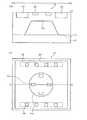
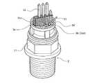
実施の形態1にかかる物理量センサ装置の構成について、圧力センサ装置を例に説明する。図1は、実施の形態1にかかる物理量センサ装置の構成を示す断面図である。図2は、図1の圧力センサチップの構成を示す説明図である。図2(1)は、圧力センサチップ11の断面図を示し、図2(2)には、圧力センサチップ11の俯瞰図を示す。図1に示すように、物理量センサ装置100は、センサエレメント1、ネジ部(被測定媒体導入部)2、インナーハウジング部(第2収容部)3およびソケットハウジング部(コネクタハウジング部(第3収容部))4を備える。本実施の形態では、センスエレメントの信号を外部に伝達するためのインタフェースとなるソケット部が、インナーハウジング部3と、ソケットハウジング部4との2つに分離する構成とする。センサエレメント1は、収納箱10、収納箱10の凹部10aに収納された、圧力センサチップ(半導体チップ)11、台座部材12、ダイアフラム13、を備える。なお、図1に示す断面は後述する図12(2)に示す断面H−H’の位置の断面である。収納箱10は、例えばステンレス鋼材(SUS)などの金属でできている。(Embodiment 1)
The configuration of the physical quantity sensor device according to the first embodiment will be described by taking a pressure sensor device as an example. FIG. 1 is a cross-sectional view showing the configuration of the physical quantity sensor device according to the first embodiment. FIG. 2 is an explanatory diagram showing the configuration of the pressure sensor chip of FIG. FIG. 2 (1) shows a cross-sectional view of the
ここで、図2(1)および図2(2)を用いて、圧力センサチップ11について説明する。図2(2)に示す断面は、図2(1)に示すQ−Q’の位置の断面である。図2(1)および図2(2)に示すように、圧力センサチップ11は、例えば、ダイアフラム11aと、4つのゲージ抵抗63と、パッド部65と、を有する。ダイアフラム11aは、半導体シリコンの第1の面61から凹加工して形成された受圧部である。第1の面61は、図1では上面である。このダイアフラム11aで圧力を受ける。4つのゲージ抵抗63は、半導体シリコンの第2の面62の、ダイアフラム11aの裏側に相当する箇所に形成されている。第2の面62は、図1では下面である。4つのゲージ抵抗63は、拡散抵抗よりなる。これらのゲージ抵抗63は、圧力センサチップ11に圧力が印加された際に第2の面62に発生する歪を抵抗値に変換する。圧力センサチップ11は他の半導体材料でできていてもよい。 Here, the
また、圧力センサチップ11には、ゲージ抵抗63によって構成されるホイートストーンブリッジ回路などの圧力センサ素子や、制御回路が形成されている。制御回路は、第2の面62の制御回路領域64に形成される。制御回路とは、圧力センサ素子の出力信号を増幅する回路、感度を補正する回路、オフセットを補正する回路、感度およびオフセットの温度特性を補正する回路などである。また、圧力センサチップ11には、サージ保護素子やフィルタ(図示省略)なども形成されている。パッド部65は、圧力センサチップ11の第2の面62上に形成されている。パッド部65に設けられた各電極は、それぞれ、ボンディングワイヤ14により後述する各リードピン(第1端子)15に接続されている。パッド部65に設けられた各電極は、金属などの配線(図示省略)によって制御回路領域64に形成された各制御回路に接続されている。すなわち、各リードピン15は、ボンディングワイヤ14およびパッド部65に設けられた各電極を介して、制御回路領域64に形成された各制御回路に接続されている。また、パッド部65と制御回路領域64は、第2の面62のうち、ダイアフラム11aが設けられた領域以外の部分に配置される。また、パッド部65は、制御回路領域64の部分に配置されてもよい。 Further, the
圧力センサチップ11の第1の面61は、収納箱10の凹部10aの底面に台座部材12を介して固着されている。台座部材12は、特に限定しないが、例えばガラス材料、すなわちパイレックス(商標登録)ガラスやテンパックスガラスなどでできている。台座部材12と圧力センサチップ11とは、静電接合によって接合されている。台座部材12と収納箱10とは、接着剤(不図示)によって接着されている。リードピン15は、センサエレメント1の信号を取り出すための端子ピンであり、複数配置される。 The
各リードピン15は、それぞれ、収納箱10の異なる貫通孔10bを通って収納箱10を貫通し、当該貫通孔10bを塞ぐ例えばガラスなどの絶縁性部材16により収納箱10に固定されている。リードピン15の一方の端部(以下、下端部とする)は、収納箱10の凹部10aから下方(ネジ部2側)に突出し、圧力センサチップ11の第2の面62上のパッド部65に設けられた各電極にボンディングワイヤ14により接続されている。リードピン15の他方の端部(以下、上端部とする)は、収納箱10の凹部10a側に対して反対側から上方(ソケットハウジング部4側)に突出している。収納箱10の凹部10a側に対して反対側には、凹み部27が設けられている。凹み部27は、絶縁性部材16に応力が集中するのを抑制するために設けられている。 Each
具体的には、複数のリードピン15のうち、電源端子、グランド端子および出力端子である各リードピン(以下、第1リードピン(第3端子)とする)15aの下端部は、それぞれ、ボンディングワイヤ14により圧力センサ素子の各電極に接続される。第1リードピン15aの上端部は、インナーハウジング部3の貫通孔3bを貫通する。 Specifically, among the plurality of lead pins 15, the lower end portions of the power supply terminal, the ground terminal, and each lead pin (hereinafter referred to as the first lead pin (third terminal)) 15a, which is an output terminal, are respectively formed by a
一方、複数のリードピン15のうち、特性調整・トリミングのための各リードピン(以下、第2リードピン(第4端子)とする)15bの下端部は、それぞれボンディングワイヤ14により所定の制御回路の各電極に接続される。第2リードピン15bは、物理量センサ装置100の組み立て途中に特性調整・トリミングを行うために用いられ、特性調整・トリミング後には用いられない。第1リードピン15aと第2リードピン15bの長さは同じである。 On the other hand, among the plurality of lead pins 15, the lower end of each lead pin (hereinafter referred to as the second lead pin (fourth terminal)) 15b for characteristic adjustment / trimming is formed by a
ここで、縦方向とは、リードピン15の軸方向である。横方向とは、リードピン15の軸方向と直交する方向である。リードピン15は、例えば42アロイ(42Alloy)や、ニッケル(Ni)を50wt%程度含み、かつ残りの割合で鉄(Fe)を含む鉄ニッケル合金(50Ni−Fe)などの金属でできている。 Here, the vertical direction is the axial direction of the
ネジ部2は、例えばSUSなどの金属でできている。ネジ部2の中心には、縦方向に被圧力測定気体である空気や被圧力測定液体である油(オイル)等の被測定媒体が通る貫通孔(導入孔)23が設けられている。ネジ部2の一方の開放端における貫通孔23の開口部が圧力導入口24である。ネジ部2の他方の開放端における貫通孔23の開口部25と収納箱10の凹部10aとが対向するように、ネジ部2の他方の開放端に設けられた台座部21上に、ダイアフラム13を挟んで収納箱10が載置されている。ネジ部2の台座部21、ダイアフラム13および収納箱10の積層箇所の周囲は、レーザー溶接により接合されている。 The
ダイアフラム13は、波打った薄い金属板であり、例えばSUSなどの金属でできている。ダイアフラム13は、収納箱10の凹部10aの開口部、および、ネジ部2の他方の開放端を塞ぐように配置される。収納箱10の凹部10aとダイアフラム13とに囲まれた空間には、圧力センサチップ11に圧力を伝達するシリコンオイルなどの液体(圧力媒体)20が充填されている。ネジ部2の台座部21、ダイアフラム13および収納箱10の積層箇所(接合部)の周囲の符号22は、ネジ部2の台座部21と収納箱10との溶接部である。符号26は、オーリングである。 The
インナーハウジング部3は、コネクタピン(第2端子)31と一体成形された樹脂部材であり、センサエレメント1の上方および周囲を囲む略凹部状をなす。具体的には、インナーハウジング部3は、収納箱10の凹部10a側に対して反対側の外周部に接着剤28により接着されている。収納箱10とインナーハウジング部3との接触面のほぼ全面に接着剤28が介在する。インナーハウジング部3と収納箱10との接着面の一方の面を凹凸が交互に繰り返し並んだ断面形状(例えばのこぎり刃のようなぎざぎざ)とし、当該接着面での接着剤の量を増やすことで、インナーハウジング部3と収納箱10とを接着しやすくしてもよい。インナーハウジング部3の凹部32は、第2リードピン15bを収容可能な深さを有する。 The
インナーハウジング部3の、センサエレメント1の上方を覆う部分(以下、インナーハウジング部3の上部とする)3aには、第1リードピン15aを貫通させるための貫通孔3bが設けられている。また、インナーハウジング部3の上部3aには、コネクタピン31が一体成形されている。コネクタピン31は、物理量センサ装置100と外部との信号のやり取りを行う信号端子である。コネクタピン31の一方の端部31a(後述する図3参照)は、インナーハウジング部3の貫通孔3bに接続する貫通孔31eを備える。コネクタピン31の垂直部31c(後述する図3参照)に設けられた凹部31fには、チップコンデンサ18が接合部材17によって取り付けられている。チップコンデンサ18は、隣り合うコネクタピン31間に取り付けられている。なお、コネクタピン31の構成は図2を用いて後述する。 A through
第1リードピン15aの上端部とコネクタピン31の一方の端部31aとは、組立て時に上方から所定の入射角(縦方向に対して3度程度傾いた角度)でレーザー光が照射される。このレーザー溶接により、第1リードピン15aの上端部は、コネクタピン31の一方の端部31aに接合されている。コネクタピン31は、例えば燐青銅(銅(Cu)に錫(Sn)を含む合金)、42アロイや50Ni−Feなどの金属でできており、レーザー光の照射によりコネクタピン31とリードピン15とが互いに溶け合うように接合される。 The upper end of the
ソケットハウジング部4は、コネクタピン31の垂直部31c(後述する図3参照)を収容した、外部配線との接続部である。ソケットハウジング部4は、コネクタピン31の垂直部31cの周囲を囲む例えば略筒状をなす。例えば、コネクタピン31は、ソケットハウジング部4の底部4bの貫通孔4cを貫通して、ソケットハウジング部4に囲まれた空間41に突出している。ソケットハウジング部4は、インナーハウジング部3の上部3aの上面の外周部に接着剤(不図示)により接着されている。インナーハウジング部3とソケットハウジング部4との接触面のほぼ全面に接着剤が介在する。ソケットハウジング部4とインナーハウジング部3との接合面に、互いに嵌合する凹凸4a,3dが設けられていてもよい。 The
ネジ部2の台座部21、収納箱10、インナーハウジング部3およびソケットハウジング部4の最大直径はほぼ等しいことが好ましい。その理由は、次の通りである。上述したように、ネジ部2、収納箱10、インナーハウジング部3およびソケットハウジング部4は順に重ねて接合(または接着)される。このため、ネジ部2の台座部21、収納箱10、インナーハウジング部3およびソケットハウジング部4の最大直径をほぼ等しくすることで直径方向(横方向)の小型化を図ることができるからである。 It is preferable that the maximum diameters of the
上述した構成の物理量センサ装置100では、圧力導入口24から圧力媒体が導入され、圧力センサチップ11のダイアフラム11aで圧力を受けると、ダイアフラム11aが変形する。そして、ダイアフラム11a上のゲージ抵抗値が変化し、それに応じた電圧信号が発生する。その電圧信号は、感度補正回路やオフセット補正回路や温度特性補正回路などの調整回路によって調整された増幅回路により増幅され、圧力センサチップ11から出力される。そして、その出力信号は、ボンディングワイヤ14を介して第1リードピン15aに出力される。 In the physical
次に、物理量センサ装置100の製造方法(組立方法)について説明する。図3〜16は、実施の形態1にかかる物理量センサ装置の製造途中(組立途中)の状態を示す説明図である。 Next, a manufacturing method (assembly method) of the physical
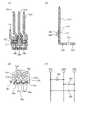
まず、図3から図5を用いてチップコンデンサ18が接続されたコネクタピン31とインナーハウジング部3について説明する。図3は、インナーハウジング部3を省いたコネクタピン31とチップコンデンサ18のみを示している。 First, the
図3(1)〜図3(3)には、各方向から見た場合のコネクタピン31を示す。図3(4)には、コネクタピン31同士を繋ぐチップコンデンサ18の等価回路を示す。第1コネクタピン31оと第4コネクタピン31rは、電源電圧を供給するための電源信号を供給する信号端子ピンであり、電源端子であるリードピン15と接続される。第2コネクタピン31pは、センサ信号を取り出すための信号端子ピンであり、出力端子であるリードピン15と接続される。第3コネクタピン31qは、グランド(Gnd)と接続するための信号端子ピンであり、グランド端子であるリードピン15と接続される。また、電源信号(Vcc)を供給するための信号端子ピンは、センサ信号(Vout)を取り出すための信号端子ピンとグランド(Gnd)と接続するための信号端子ピンとのそれぞれとの間にチップコンデンサ18を取り付けるために、第1コネクタピン31оと第4コネクタピン31rのように両端に2本設けられる。 3 (1) to 3 (3) show the connector pins 31 when viewed from each direction. FIG. 3 (4) shows an equivalent circuit of a
第1コネクタピン31o〜第3コネクタピン31qは、樹脂形成によってインナーハウジング部3の上部3aに埋め込まれる部分(以下、水平部(第1部分)とする)31bと、当該水平部31bに連結され、当該水平部31bと直交して上方に突出する部分(以下、垂直部とする)31cと、からなる略L字状の断面形状を有する(図3(3)の例では第1コネクタピン31oを示す)。第4コネクタピン31rについては、垂直部31cのみを有する略I字状の断面形状を有する(不図示)。 The first connector pins 31o to the third connector pins 31q are connected to a portion (hereinafter referred to as a horizontal portion (first portion)) 31b embedded in the
第1コネクタピン31o〜第3コネクタピン31qの一方の端部31aは、貫通孔31eの周囲を囲むように成形される(図3(2))。なお、第1コネクタピン31o〜第3コネクタピン31qの端部31aは、貫通孔31eの周囲の一部を囲む略半円状の平面形状に成形されてもよいし、貫通孔31eの側壁に達する直線状の平面形状を有し、当該貫通孔31eの側壁の一部に露出されていてもよい(不図示)。 One
また、第1コネクタピン31oの水平部31bは、第1コネクタピン31oの端部31aと、第2コネクタピン31pの水平部31bおよび端部31aと、第3コネクタピン31qの水平部31bおよび端部31aを囲うように設けられ、第4コネクタピン31rと一体化されて接続されている(図3(2))。これにより、第1コネクタピン31oと第4コネクタピン31rとは同電位となる。 Further, the
まず、コネクタピン31に半田や導電性接着剤などの接合部材17によってチップコンデンサ18を取り付ける。例えば、第1コネクタピン31oと第2コネクタピン31pとがチップコンデンサ18aを介して接続されている(図3(1)、図3(2))。例えば、第2コネクタピン31pと第3コネクタピン31qとがチップコンデンサ18bを介して接続されている(図3(1)、図3(2))。例えば、第3コネクタピン31qと第4コネクタピン31rとがチップコンデンサ18cを介して接続されている(図3(1)、図3(2))。このように、コネクタピン31同士は、チップコンデンサ18を介して接続されている(図3(1)、図3(2))。上述したように、第1コネクタピン31oの端部31aが第4コネクタピン31rの垂直部31cと接続されている。このため、各端子間にチップコンデンサ18を取り付けることができる(図3(4))。 First, the
図3の例では、各端子間にチップコンデンサ18を取り付けているが、これに限らない。例えば、第4コネクタピン31rと第3コネクタピン31qとの間のチップコンデンサ18cについては、サージの要求に応じて取り付けるか否かが決定されてもよい。例えば、チップコンデンサ18cが取り付けられる場合、チップコンデンサ18cが取り付けられない場合と比較してEMC(Electromagnetic Cоmpatibility)耐性が向上する。 In the example of FIG. 3, a
次に、コネクタピン31を、インナーハウジング部3の成形用の金型に入れる。そして、その金型に樹脂材料を流し込むことによりインナーハウジング部3とコネクタピン31とを一体成形(インサート成形)する。 Next, the
図4には、インナーハウジング部3の断面を示す。図5には、インナーハウジング部の外観を示す。インナーハウジング部3には、ソケットハウジング部4との接合面に嵌合する凹3dが設けられている(図4,図5(1),図5(2))。 FIG. 4 shows a cross section of the
インナーハウジング部3の上部3aには、第1リードピン15aを貫通させるための貫通孔3bが設けられている(図5(2))。貫通孔3bは、コネクタピン31の貫通孔31e(図3参照)と同じ位置に設けられている。このため、インナーハウジング部3のコネクタピン31が露出している側から見た表面の貫通孔3bは、貫通孔31eと同じである。ただし、後述する図12に示すようにインナーハウジング部3のコネクタピン31が露出している側から見た裏面の貫通孔3bは樹脂によって形成された貫通孔である。また、インナーハウジング部3の上部3aには、コネクタピン31が一体成形されている(図4,図5(1),図5(2))。例えば、インナーハウジング部3からコネクタピン31の垂直部31cの一部が露出されている(図4)。例えば、インナーハウジング部3の上部3aは、コネクタピン31の水平部31bを被覆する。コネクタピン31の一方の端部31aは、インナーハウジング部3の上部3aから露出されている。この、コネクタピン31の一方の端部31aの露出されている部分と第1リードピン15aが溶接される。 A through
また、インナーハウジング部3の上端部3eは、コネクタピン31に取り付けたチップコンデンサ18および接合部材17を被覆する。 Further, the
次に、図6から図11を用いて、収納箱10にリードピンを取り付ける工程から圧力媒体を注入して封止するまでの工程について説明する。 Next, the steps from attaching the lead pin to the
図6に示すように、収納箱10の各貫通孔10bに、それぞれリードピン15を貫通させる。ここでは、収納箱10が略円形状の平面形状を有し、収納箱10の凹部10aの底面の中心を中心とする円周上に貫通孔10bが設けられている場合を例に説明する。複数の孔のうち、1つの孔は圧力媒体であるオイルを注入するための孔10cであり、残りの孔がリードピン15を貫通させる貫通孔10bである。 As shown in FIG. 6, the
次に、収納箱10の貫通孔10bにガラスなどの絶縁性部材16を流し込んでリードピン15と収納箱10とを接合(気密封止)する。次に、収納箱10の凹部10aの底面の、貫通孔10bが設けられていない例えば中心に接着剤51を塗布する。次に、図7に示すように、収納箱10の凹部10aの底面の接着剤51上に、圧力センサチップ11を搭載して接着する。次に、図8に示すように、圧力センサチップ11の各電極とリードピン15とをボンディングワイヤ14により電気的に接続する。次に、図9に示すように、ネジ部2の台座部21上に、ダイアフラム13を挟んで、凹部10a側が下(ネジ部2側)になるように収納箱10を載置し、これらの部材の積層部分を例えばレーザーシーム溶接により接合する。 Next, an insulating
次に、図10に示すように、真空雰囲気下で、収納箱10の孔10cから収納箱10の凹部10aとダイアフラム13とに囲まれた空間にシリコンオイルなどの液体20を注入する。次に、図11に示すように、液体20を注入した孔10cに例えばSUSなどの金属でできた金属球52を押し当てて電圧を加える。これにより、当該孔10cの開口部に金属球52が溶接され(抵抗溶接)、液体20が封止される。次に、一般的な方法により、センサエレメント1の特性調整・トリミングを行う。 Next, as shown in FIG. 10, a liquid 20 such as silicone oil is injected from the
次に、図12から図14を用いて、インナーハウジング部3と収納箱10とを接着する工程について説明する。 Next, a step of adhering the
図12(1)には、インナーハウジング部3のコネクタピン31が露出していない側の底面を示す。また、図12(2)には、収納箱10のリードピン15が露出している側の面を示す。 FIG. 12 (1) shows the bottom surface of the
図12(1)の例では、インナーハウジング部3には、3つの貫通孔3bと、5つの溝3fとを有する。貫通孔3bは、上述したようにコネクタピン31と接続されている。貫通孔3bには第1リードピン15aが貫通されてコネクタピン31と接続される。溝3fは、第1溝3faと第2溝3fbとがある。溝3fには第2リードピン15bが嵌め込まれる。リードピン15の長さが8mm程度である場合、溝3fと第2リードピン15bとが嵌め込まれる長さは2mm以上3mm以下程度である。 In the example of FIG. 12 (1), the
リードピン15の横方向の断面(リードピン15を輪切りに切断した断面)の形状が円形形状であるため、貫通孔3bと第1溝3faの形状は円形形状である。貫通孔3bと第1溝3faの径はφhである。リードピン15の径はφpである。φp≒φhの関係が成り立つ。 Since the cross section of the
第2溝3fbの形状は、第2溝3fbの対辺の長さが長さφpより短くなるような形状であれば、第2溝3fbに第2リードピン15bが嵌め込まれる。また、第2溝3fbの形状は、第2リードピン15bを押し込む力の限界を超えない様な形状である。図12(1)の例では、第2溝3fbの形状は弦と円弧を組み合わせた形状である。なお、第2溝3fbの形状は略六角形形状や略四角形形状などのように多角形の形状であってもよい。例えば第2溝3fbの弧の長さはφh’である。φh’<φpの関係が成り立つ。例えば、第2溝3fbや第2リードピン15bの寸法精度のばらつきを考慮して、φh’をφpよりも5%以上10%以下程度減らしている。なお、φh’=φpであると、第2溝3fbに第2リードピン15bを嵌め込む際に第2リードピン15bが削られるため、精度よく嵌め込むことができない虞があるため、φh’<φpとすることが好ましい。 If the shape of the second groove 3fb is such that the length of the opposite side of the second groove 3fb is shorter than the length φp, the
また、第2溝3fbの数が多いと、第2溝3fbに第2リードピン15bを押し込むための力が大きくなるため、第2リードピン15bを押し込むことができない虞がある。そこで、第2溝3fbの数は1個以上3個以下とすることが好ましい。第2溝3fbの数は、1個よりも2個がよく、2個よりも3個であるとよい。第2溝3fbの数が3個であると、面固定となるため、インナーハウジング部3の浮き上がりを抑制することができる。また、溝3fの形状を第2溝3fbとすることが好ましいが、貫通孔3bの形状が第2溝3fbの形状となっていてもよい。例えば、5本の第2リードピン15bをすべて切断してしまう場合、第2リードピン15bを溝3fに嵌め込めないため、3個の貫通孔3bのうち少なくともいずれかの貫通孔3bの形状を第2溝3fbの形状としてもよい。また、例えば、面固定となるように第2溝3fbの数を3個としたいが、5本の第2リードピン15bのうち3本の第2リードピン15bを切断して2本の第2リードピン15bのみ溝3fに嵌め込めない場合、3個の貫通孔3bのうちの1個の貫通孔3bの形状を第2溝3fbの形状としてもよい。 Further, if the number of the second groove 3fb is large, the force for pushing the
このように、例えば複数の溝3fのうちの一部の溝3fの形状を円形形状から、円形の直径よりも対辺の長さが短くなるような形状に変更することにより、溝3fにリードピン15が噛み込むような構造となる。このため、接着剤28(図1)の熱硬化時のインナーハウジング部3の浮き上がりを抑制することができる。換言すると、接着剤28の熱硬化時に、インナーハウジング部3の底面3cと収納箱10とに隙間が形成されることを抑制することができる。 In this way, for example, by changing the shape of a part of the
次に、図13に示すように、コネクタピン31を一体成形したインナーハウジング部3の貫通孔3bに第1リードピン15aを貫通させ、インナーハウジング部3の溝3fに第2リードピン15bを嵌め込ませることにより、インナーハウジング部3の位置を決定し、熱硬化の接着剤28(図1)でインナーハウジング部3を収納箱10に固定する。例えば、塗布した接着剤28が硬化するまでに、インナーハウジング部3と収納箱10とを高温状態で放置する。この際、第2リードピン15bがインナーハウジング部3の溝3fに嵌め込まれているため、接着剤28の熱硬化時のインナーハウジング部3の浮き上がりを防止することができ、インナーハウジング部3と収納箱10とを押さえ込まなくてもよい。このように、簡易に組み立てることができる。 Next, as shown in FIG. 13, the
このとき、第1リードピン15aは、インナーハウジング部3の上部3aの上面に露出するコネクタピン31とインナーハウジング部3の貫通孔3bで接触する。また、この段階では、コネクタピン31の周囲を覆うソケットハウジング部4が接合されていないため、インナーハウジング部3の上方に、レーザー光53の進入経路上に障害物となる部材は配置されていない。すなわち、ほぼ上方から、第1リードピン15aの上端部とコネクタピン31の一方の端部31aとの接触部を視認可能である。次に、インナーハウジング部3の貫通孔3bに上方から所定の入射角でレーザー光53を照射し、第1リードピン15aの上端部とコネクタピン31の一方の端部31aとの接触部を溶接(接合)する。 At this time, the
図14には、接着した後のインナーハウジング部3と収納箱10との断面を示す。断面は図12(2)に示した断面A−A’の位置の断面である。なお、図14ではネジ部2や圧力センサチップ11などを省略してある。第1リードピン15aはコネクタピン31に溶接される。具体的には、例えば第1リードピン15aの上端部は、貫通孔を貫通し、コネクタピン31の一方の端部31aおよびコネクタピン31の水平部31bと接合されている。一方、第2リードピン15bと溝3fとが嵌合している。また、第2リードピン15bは切断されないため、第2リードピン15bと第1リードピン15aとは同じ長さである。 FIG. 14 shows a cross section of the
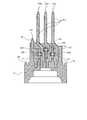
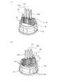
次に、図15を用いて、ソケットハウジング部4について説明する。 Next, the
図15(1)には、ソケットハウジング部4の斜視図を示す。図15(2)には、ソケットハウジング部4の断面図を示す。ソケットハウジング部4は、コネクタピン31の垂直部31cを収容する。ソケットハウジング部4は、インナーハウジング部3と接合する面にインナーハウジング部3の凹3dと嵌合する凸4aが設けられている。 FIG. 15 (1) shows a perspective view of the
また、ソケットハウジング部4は、内部が凹部になっている。ソケットハウジング部4の凹部の底部4bには、貫通孔4cと溝4dとが設けられている。底部4bには、ソケットハウジング部4の内壁に近い部分に溝4dが設けられるため、底部4bの溝4dが設けられる部分は貫通孔4cが設けられている部分よりも厚みがある。各貫通孔4cには、第1コネクタピン31o〜第3コネクタピン31qが貫通される。溝4dには、第4コネクタピン31rが入れられる。また、各貫通孔4cと溝4dとは、インナーハウジング部3の底面3cも含めてコネクタピン31を貫通または入れることが可能な形状となっている。溝4dおよび貫通孔4cの位置によってインナーハウジング部3の位置を決定することができる。 Further, the
次に、図16を用いて、ソケットハウジング部4とインナーハウジング部3とを接合する工程について説明する。 Next, a step of joining the
図16に示すように、接着剤によりソケットハウジング部4とインナーハウジング部3とを接合する。これにより、コネクタピン31の周囲を囲むように、インナーハウジング部3の上部3aの上面にソケットハウジング部4が接合される。このとき、例えば、各貫通孔4cには、それぞれ第1コネクタピン31o〜第3コネクタピン31qが貫通される。溝4dに第4コネクタピン31rを入れ、各貫通孔4cには、それぞれ第1コネクタピン31o〜第3コネクタピン31qを貫通させることにより、インナーハウジング部3とソケットハウジング部4とが接合される。 As shown in FIG. 16, the
その後、ネジ部2の台座部21の下面にオーリング26(図1)を装着することで、図1に示す物理量センサ装置100が完成する。 After that, by mounting the O-ring 26 (FIG. 1) on the lower surface of the
以上、説明したように、本実施の形態1によれば、リードピンを収容するインナーハウジング部の一部の穴の形状を、穴の対辺の長さが当該穴に収容されるリードピンの径よりも短くすることで、一部の穴とリードピンとが嵌合するため、リードピンが配置されたセンサエレメントと、インナーハウジング部とを熱硬化の接着剤によって固定するための熱硬化中に、センサエレメントからのインナーハウジング部の浮き上がりによる隙間の発生を抑制することができる。これにより、熱硬化中にセンサエレメントとインナーハウジング部とを押さえつける工程を行うことなく、センサエレメントとインナーハウジング部との接着を安定させることができ、簡易に組み立てることができる。したがって、接着強度の向上と強度の安定化を図ることができ、物理量センサ装置の製造ばらつきを抑制することができる。 As described above, according to the first embodiment, the shape of a part of the hole of the inner housing portion accommodating the lead pin is set so that the length of the opposite side of the hole is larger than the diameter of the lead pin accommodated in the hole. By shortening, some holes and lead pins are fitted, so that the sensor element on which the lead pins are placed and the inner housing portion are fixed from the sensor element during thermosetting for fixing with a thermosetting adhesive. It is possible to suppress the generation of a gap due to the lifting of the inner housing portion of the. As a result, the adhesion between the sensor element and the inner housing portion can be stabilized without performing the step of pressing the sensor element and the inner housing portion during heat curing, and the assembly can be easily performed. Therefore, the adhesive strength can be improved and the strength can be stabilized, and the manufacturing variation of the physical quantity sensor device can be suppressed.
また、出力端子、電源端子、グランド端子などのように外部と信号を入出力するためのリードピンはインナーハウジング部のコネクタピンとレーザー溶接されるが、そのリードピンに傷が付いていると、レーザー溶接がし難い。そこで、本実施の形態1によれば、形状を変更する穴に収容されるリードピンは、センサの特性調整・トリミングを行うためのリードピンであり、物理量センサ装置の実使用時には使用されない。これにより、出力端子、電源端子、グランド端子などのように外部と信号を入出力されるためのリードピンンに傷を付けることなく、センサエレメントとインナーハウジング部との接着を安定させることができる。 In addition, lead pins for inputting and outputting signals to the outside, such as output terminals, power supply terminals, and ground terminals, are laser welded to the connector pins of the inner housing, but if the lead pins are scratched, laser welding will occur. It's hard to do. Therefore, according to the first embodiment, the lead pin accommodated in the hole for changing the shape is a lead pin for adjusting the characteristics of the sensor and trimming, and is not used in the actual use of the physical quantity sensor device. As a result, it is possible to stabilize the adhesion between the sensor element and the inner housing portion without damaging the lead pins for inputting / outputting signals to / from the outside such as the output terminal, the power supply terminal, and the ground terminal.
また、形状を変更する一部の穴の数は、1個以上3個以下であることが好ましい。これにより、嵌め込み易さを維持しつつ、センサエレメントからのインナーハウジング部の浮き上がりを抑制することができる。特に一部の穴の数が3個であれば、面固定となるため、センサエレメントからのインナーハウジング部の浮き上がりをより抑制することができる。また、例えば、コネクタピンの断面形状が円形形状である場合に、ソケットハウジング部の一部の穴以外の残余の穴の形状は円形形状であり、一部の穴の形状は、多角形や弦と円弧を組み合わせた形状である。 Further, the number of some holes whose shape is changed is preferably 1 or more and 3 or less. As a result, it is possible to suppress the lifting of the inner housing portion from the sensor element while maintaining the ease of fitting. In particular, when the number of some holes is three, the surface is fixed, so that the lifting of the inner housing portion from the sensor element can be further suppressed. Further, for example, when the cross-sectional shape of the connector pin is circular, the shape of the remaining holes other than some holes of the socket housing portion is circular, and the shape of some holes is polygonal or string. It is a shape that combines and arc.
(実施の形態2)
次に、実施の形態2にかかる物理量センサ装置の製造方法について説明する。図17は、実施の形態2にかかる物理量センサ装置の製造途中(組立途中)の状態を示す説明図である。実施の形態2にかかる物理量センサ装置の製造方法が実施の形態1にかかる物理量センサ装置の製造方法と異なる点は、コネクタピン31のチップコンデンサ18を取り付けるための部分が露出された窓部3gが形成されるようにインナーハウジング部3とコネクタピン31とを一体成形し、インナーハウジング部3の窓部3gに露出するコネクタピン31にチップコンデンサ18を取り付けた後に、当該窓部3gを樹脂で埋める点である。(Embodiment 2)
Next, a method of manufacturing the physical quantity sensor device according to the second embodiment will be described. FIG. 17 is an explanatory diagram showing a state during manufacturing (during assembly) of the physical quantity sensor device according to the second embodiment. The difference between the manufacturing method of the physical quantity sensor device according to the second embodiment and the manufacturing method of the physical quantity sensor device according to the first embodiment is that the
具体的には、コネクタピン31を、インナーハウジング部3の成形用の金型に入れる。そして、その金型に樹脂材料を流し込むことによりインナーハウジング部3とコネクタピン31とを一体成形する。これにより、図17に示すように、窓部3gが設けられたインナーハウジング部3の上端部3eが形成される。次に、図17に示すように、窓部3gに露出するコネクタピン31の凹部31fに、接合部材17によってチップコンデンサ18を取り付ける。次に、窓部3gに樹脂部材を流し込むことにより窓部3gを樹脂で埋める。これにより、上述した図5(1)に示したように、コネクタピン31に取り付けたチップコンデンサ18および接合部材17が樹脂によって被覆されたインナーハウジング部3が得られる。 Specifically, the
実施の形態2にかかる物理量センサ装置の製造方法におけるインナーハウジング部3とコネクタピン31とを一体成形する工程と、コネクタピン31にチップコンデンサ18を取り付ける工程と、窓部3gを樹脂で埋める工程とは、実施の形態1にかかる物理量センサ装置の製造方法においてコネクタピン31にチップコンデンサ18を取り付ける工程と、チップコンデンサ18を取り付けた後にインナーハウジング部3とコネクタピン31とを一体成形する工程と、の代わりに行われる。また、実施の形態2にかかる物理量センサ装置の製造方法においてこれらの工程以外の工程については、実施の形態1にかかる物理量センサ装置の製造方法と同様であるため、詳細な説明を省略する。 The step of integrally molding the
以上において本発明は、上述した実施の形態1,2に限らず、本発明の趣旨を逸脱しない範囲で種々変更可能である。例えば、上述した各実施の形態では圧力センサ装置を例に説明しているが、上述した各実施の形態に限らず、例えば、加速度、ジャイロ(角度や角速度)、流量および温度など圧力以外の物理量を検出する物理量センサ装置にも適用可能である。また、上述した各実施の形態では、歪ゲージ式の圧力センサチップを例に説明しているが、半導体ピエゾ抵抗式、静電容量式およびシリコンレゾナント式の圧力センサチップも適用可能である。 In the above, the present invention is not limited to the above-described first and second embodiments, and various modifications can be made without departing from the spirit of the present invention. For example, although the pressure sensor device is described as an example in each of the above-described embodiments, the physical quantities other than pressure such as acceleration, gyro (angle and angular velocity), flow rate, and temperature are not limited to the above-described embodiments. It can also be applied to a physical quantity sensor device that detects. Further, in each of the above-described embodiments, the strain gauge type pressure sensor chip is described as an example, but a semiconductor piezoresistive type, a capacitance type and a silicon resonant type pressure sensor chip can also be applied.
また、例えば、上述した実施の形態1,2では、チップコンデンサがインナーハウジング部のコネクタピンの端部に設けられている例を用いて説明しているが、インナーハウジング部の凹部内にノイズ対策用基板を介してノイズ対策用のチップコンデンサが設けられていてもよい。そして、ノイズ対策用基板には、例えば、第1リードピンおよび第2リードピンの少なくとも一部を貫通させるための貫通孔が設けられている。この貫通孔の周囲に設けられたランド(不図示)に第1リードピンが半田付けされている。ノイズ対策用基板は、貫通孔を貫通する第1リードピンに固定され、収納箱に対する配置(縦方向および横方向)が決定される。また、ノイズ対策用基板の貫通孔に少なくとも一部の第2リードピンを貫通させて、当該第2リードピンによってノイズ対策用基板を固定してもよい。この場合、第2リードピンが貫通する貫通孔の周囲にランドを設けなくてもよい。一部の第2リードピンは、例えば、3本の第2リードピンであることが好ましい。また、チップコンデンサは、ノイズ対策用基板の上面(縦方向に収納箱に対向する面に対して反対側の面)に配置され、配線パターンおよびランドを介して第1リードピンに電気的に接続されている。また、ノイズ対策用基板の貫通孔に貫通されない第2リードピンの上端部は、特性調整・トリミング後に、インナーハウジング部の凹部内に収まる程度の長さに短く切断されていてもよい。 Further, for example, in the above-described first and second embodiments, the chip capacitor is described by using an example in which the chip capacitor is provided at the end of the connector pin of the inner housing portion, but noise countermeasures are provided in the recess of the inner housing portion. A chip capacitor for noise suppression may be provided via the housing board. The noise suppression substrate is provided with, for example, through holes for penetrating at least a part of the first lead pin and the second lead pin. The first lead pin is soldered to a land (not shown) provided around the through hole. The noise suppression substrate is fixed to the first lead pin penetrating the through hole, and the arrangement (vertical direction and horizontal direction) with respect to the storage box is determined. Further, at least a part of the second lead pins may be passed through the through holes of the noise suppression substrate, and the noise suppression substrate may be fixed by the second lead pins. In this case, it is not necessary to provide a land around the through hole through which the second lead pin penetrates. Some second lead pins are preferably, for example, three second lead pins. Further, the chip capacitor is arranged on the upper surface of the noise suppression board (the surface opposite to the surface facing the storage box in the vertical direction), and is electrically connected to the first lead pin via the wiring pattern and the land. ing. Further, the upper end portion of the second lead pin that does not penetrate through the through hole of the noise suppression substrate may be cut short to a length that fits in the recess of the inner housing portion after characteristic adjustment and trimming.
また、例えば、上述した実施の形態1,2では、インナーハウジング部とソケットハウジング部の2つの部材を用いた例を説明した。これは、第1リードピンとコネクタピンとをレーザー溶接する場合に、ソケットハウジング部を取り付ける前に第1リードピンとコネクタピンとのレーザー溶接を行うことにより溶接を容易とするものである。しかし、物理量センサ装置が十分大きく、ソケットハウジング部を取り付けた後に第1リードピンとコネクタピンとのレーザー溶接を行うことができる場合は、インナーハウジング部とソケットハウジング部を一体に樹脂成形することができる。この場合、インナーハウジング部とソケットハウジング部とを一体に成形する際、チップコンデンサを取り付けたコネクタピンをインサート成形することができる。インナーハウジング部とソケットハウジング部とが一体成形されたハウジング部(第1収容部)を有する物理量センサ装置の製造方法では、チップコンデンサを接合部材により取り付けたコネクタピンを、ハウジング部の成形用の金型に入れ、その金型に樹脂部材を流し込むことにより、インナーハウジング部とソケットハウジング部とを合わせたハウジング部とコネクタピンとを一体成形することができる。 Further, for example, in the above-described first and second embodiments, an example using two members, an inner housing portion and a socket housing portion, has been described. In this method, when the first lead pin and the connector pin are laser-welded, the welding is facilitated by performing the laser welding between the first lead pin and the connector pin before attaching the socket housing portion. However, if the physical quantity sensor device is sufficiently large and the first lead pin and the connector pin can be laser-welded after the socket housing portion is attached, the inner housing portion and the socket housing portion can be integrally resin-molded. In this case, when the inner housing portion and the socket housing portion are integrally molded, the connector pin to which the chip capacitor is attached can be insert-molded. In the method of manufacturing a physical quantity sensor device having a housing portion (first accommodating portion) in which an inner housing portion and a socket housing portion are integrally molded, a connector pin to which a chip capacitor is attached by a joining member is attached to a metal for molding the housing portion. By putting it in a mold and pouring a resin member into the mold, the housing portion in which the inner housing portion and the socket housing portion are combined and the connector pin can be integrally molded.
以上のように、本発明にかかる物理量センサ装置の製造方法および物理量センサ装置は、収納箱の凹部側(ダイアフラム側)から圧力を印加するセンサチップを備えた物理量センサ装置に有用であり、特に圧力センサ装置に適している。 As described above, the method for manufacturing a physical quantity sensor device and the physical quantity sensor device according to the present invention are useful for a physical quantity sensor device provided with a sensor chip that applies pressure from the concave side (diaphragm side) of the storage box, and particularly the pressure. Suitable for sensor devices.
1 センサエレメント
2 ネジ部(被測定媒体導入部)
3 インナーハウジング部
3a インナーハウジング部の上部
3b インナーハウジング部の貫通孔
3c インナーハウジング部の上端部の底面
3d インナーハウジング部の上部の外周部の凹凸
3e インナーハウジング部の上端部
3f,3fa,3fb インナーハウジング部の溝
4 ソケットハウジング部
4a ソケットハウジング部の下端部の凹凸
4b ソケットハウジング部の底部
4c ソケットハウジング部の底部の貫通孔
4d ソケットハウジング部の底部の溝
10 収納箱
10a 収納箱の凹部
10b 収納箱の貫通孔
10c 収納箱の孔
11 圧力センサチップ
11a,13 ダイアフラム
12 台座部材
14 ボンディングワイヤ
15,15a,15b リードピン
16 絶縁性部材
17 接合部材
18,18a〜18c チップコンデンサ
20 液体
21 台座部
22 溶接部
23 ネジ部の貫通孔
24 ネジ部の一方の開放端の圧力導入口(導入孔)
25 ネジ部の他方の開放端の開口部
26 オーリング
27 凹み部
28,51 接着剤
31,31o〜31r コネクタピン
31a コネクタピンの端部
31b コネクタピンの水平部
31c コネクタピンの垂直部
31e コネクタピンの貫通孔
31f コネクタピンの凹部
32 インナーハウジング部の凹部
41 ソケットハウジング部に囲まれた空間
52 金属球
53 レーザー光
61 第1の面
62 第2の面
63 ゲージ抵抗
64 制御回路領域
65 パッド部
100 物理量センサ装置1
3
25 Opening at the other open end of the threaded part 26 O-
Claims (12)
Translated fromJapanese前記センサエレメントに前記第1収容部を熱硬化の接着剤によって固定する第1工程を含み、
前記第1収容部の前記各第1端子を収容可能な各穴のうちの一部の穴の断面形状は、当該穴の断面の対辺の長さが当該穴に対応する第1端子の径よりも短いことを特徴とする物理量センサ装置の製造方法。The introduction hole on the pedestal portion provided at one end of the introduction hole of the measurement medium introduction part and the introduction hole for guiding the measurement medium which is the pressure measurement gas or the pressure measurement liquid. The sensor element is sandwiched between the sensor element fixed so as to block the first terminal and the first terminal to be measured is arranged, and the first terminal is accommodated and connected to an external wiring. In a method of manufacturing a physical quantity sensor device including a first accommodating portion in which a second terminal serving as a portion is arranged.
The sensor element includes a first step of fixing the first housing portion with a thermosetting adhesive.
The cross-sectional shape of some of the holes that can accommodate each of the first terminals of the first accommodating portion is such that the length of the opposite side of the cross section of the hole is larger than the diameter of the first terminal corresponding to the hole. A method for manufacturing a physical quantity sensor device, which is characterized by being short.
前記各第1端子は、前記制御回路と前記第2端子とを電気的に接続する第3端子と前記制御回路の調整および/またはトリミング用の第4端子とを有し、
前記一部の穴は、前記第4端子の一部の端子を収容可能な穴であることを特徴とする請求項1〜3のいずれか一つに記載の物理量センサ装置の製造方法。A sensor element and a sensor chip provided with a control circuit electrically connected to the sensor element are arranged on the sensor element.
Each of the first terminals has a third terminal that electrically connects the control circuit and the second terminal, and a fourth terminal for adjusting and / or trimming the control circuit.
The method for manufacturing a physical quantity sensor device according to any one of claims 1 to 3, wherein the partial hole is a hole capable of accommodating a partial terminal of the fourth terminal.
前記各第1端子は、前記制御回路と前記第2端子とを電気的に接続する第3端子と前記制御回路の調整および/またはトリミング用の第4端子とを有し、
前記各穴のうち前記第3端子を収容可能な穴は、貫通孔であり、
前記各穴のうち前記第4端子を収容可能な穴は、溝であり、
前記第2端子は、前記第1収容部に一体化され、前記第1収容部の内部で前記第1収容部の前記貫通孔と接続された第1部分を有し、
前記第1工程では、
前記第3端子を前記第1収容部の前記貫通孔に貫通させ、前記第4端子を前記第1収容部の前記溝に入れることを特徴とする請求項1〜4のいずれか一つに記載の物理量センサ装置の製造方法。A sensor element and a sensor chip provided with a control circuit electrically connected to the sensor element are arranged on the sensor element.
Each of the first terminals has a third terminal that electrically connects the control circuit and the second terminal, and a fourth terminal for adjusting and / or trimming the control circuit.
Of the holes, the hole that can accommodate the third terminal is a through hole.
Of the holes, the hole that can accommodate the fourth terminal is a groove.
The second terminal has a first portion integrated with the first accommodating portion and connected to the through hole of the first accommodating portion inside the first accommodating portion.
In the first step,
The invention according to any one of claims 1 to 4, wherein the third terminal is passed through the through hole of the first accommodating portion, and the fourth terminal is inserted into the groove of the first accommodating portion. Manufacturing method of physical quantity sensor device.
前記被測定媒体導入部との間に前記センサエレメントを挟み込み、かつ前記各第1端子を収容し、外部配線との接続部となる前記第2端子が配置される第2収容部と、前記センサエレメントとの間に前記第2収容部を挟み込みかつ前記第2端子を収容する第3収容部と、からなることを特徴とする請求項1〜5のいずれか一つに記載の物理量センサ装置の製造方法。The first housing unit
A second accommodating portion in which the sensor element is sandwiched between the sensor element to be measured and the first terminal is accommodated and the second terminal serving as a connection portion with an external wiring is arranged, and the sensor. The physical quantity sensor device according to any one of claims 1 to 5, wherein the second accommodating portion is sandwiched between the element and a third accommodating portion for accommodating the second terminal. Production method.
前記台座部上に前記導入孔を塞ぐように固定されたセンサエレメントと、
前記センサエレメントに配置された各第1端子と、
前記被測定媒体導入部との間に前記センサエレメントを挟み込み、かつ前記各第1端子を収容し、前記センサエレメントに固定された第1収容部と、
前記第1収容部に配置されて前記各第1端子のうちの一部の端子に接合された、外部配線との接続部となる第2端子と、
を備え、
前記第1収容部の前記各第1端子を収容可能な各穴のうちの一部の穴の断面形状は、当該穴の断面の対辺の長さが当該穴に対応する第1端子の径よりも短いことを特徴とする物理量センサ装置。A measurement medium introduction unit having an introduction hole for guiding a measurement medium which is a pressure measurement gas or a pressure measurement liquid and having a pedestal portion provided at one end of the introduction hole.
A sensor element fixed on the pedestal portion so as to close the introduction hole,
Each first terminal arranged on the sensor element and
A first accommodating portion in which the sensor element is sandwiched between the sensor element to be measured and the first terminals are accommodated and fixed to the sensor element.
A second terminal, which is arranged in the first accommodating portion and is joined to a part of the terminals of the first terminals, and serves as a connection portion with external wiring.
With
The cross-sectional shape of some of the holes capable of accommodating the first terminals of the first accommodating portion is such that the length of the opposite side of the cross section of the holes is larger than the diameter of the first terminals corresponding to the holes. A physical quantity sensor device characterized by being short.
前記各第1端子は、前記制御回路と前記第2端子とを電気的に接続する第3端子と前記制御回路の調整および/またはトリミング用の第4端子とを有し、
前記一部の穴は、前記第4端子の一部の端子を収容可能な穴であることを特徴とする請求項7〜9のいずれか一つに記載の物理量センサ装置。A sensor element and a sensor chip provided with a control circuit electrically connected to the sensor element are arranged on the sensor element.
Each of the first terminals has a third terminal that electrically connects the control circuit and the second terminal, and a fourth terminal for adjusting and / or trimming the control circuit.
The physical quantity sensor device according to any one of claims 7 to 9, wherein the partial hole is a hole capable of accommodating a partial terminal of the fourth terminal.
前記各第1端子は、前記制御回路と前記第2端子とを電気的に接続する第3端子と前記制御回路の調整および/またはトリミング用の第4端子とを有し、
前記各穴のうち前記第3端子を収容可能な穴は貫通孔であり、
前記各穴のうち前記第4端子を収容可能な穴は溝であり、
前記第2端子は、前記第1収容部に一体化され、前記第1収容部の前記貫通孔に露出された第1部分を有し、
前記第3端子は、前記第1収容部の前記貫通孔を貫通し、前記第1部分で前記第2端子と電気的に接続され、
前記第4端子は、前記第1収容部の前記溝に入れられていることを特徴とする請求項7〜10のいずれか一つに記載の物理量センサ装置。A sensor element and a sensor chip provided with a control circuit electrically connected to the sensor element are arranged on the sensor element.
Each of the first terminals has a third terminal that electrically connects the control circuit and the second terminal, and a fourth terminal for adjusting and / or trimming the control circuit.
Of the holes, the hole that can accommodate the third terminal is a through hole.
Of the holes, the hole that can accommodate the fourth terminal is a groove.
The second terminal has a first portion integrated with the first accommodating portion and exposed to the through hole of the first accommodating portion.
The third terminal penetrates the through hole of the first accommodating portion and is electrically connected to the second terminal at the first portion.
The physical quantity sensor device according to any one of claims 7 to 10, wherein the fourth terminal is formed in the groove of the first accommodating portion.
前記被測定媒体導入部との間に前記センサエレメントを挟み込み、かつ前記各第1端子を収容し、外部配線との接続部となる前記第2端子が配置される第2収容部と、前記センサエレメントとの間に前記第2収容部を挟み込みかつ前記第2端子を収容する第3収容部と、からなることを特徴とする請求項7〜11のいずれか一つに記載の物理量センサ装置。The first housing unit
A second accommodating portion in which the sensor element is sandwiched between the sensor element to be measured and the first terminal is accommodated and the second terminal serving as a connection portion with an external wiring is arranged, and the sensor. The physical quantity sensor device according to any one of claims 7 to 11, further comprising a third accommodating portion that sandwiches the second accommodating portion between the element and accommodating the second terminal.
Priority Applications (2)
| Application Number | Priority Date | Filing Date | Title |
|---|---|---|---|
| JP2017032740AJP6809284B2 (en) | 2017-02-23 | 2017-02-23 | Manufacturing method of physical quantity sensor device and physical quantity sensor device |
| US15/866,028US10852318B2 (en) | 2017-02-23 | 2018-01-09 | Method of manufacturing physical quantity sensor device and physical quantity sensor device |
Applications Claiming Priority (1)
| Application Number | Priority Date | Filing Date | Title |
|---|---|---|---|
| JP2017032740AJP6809284B2 (en) | 2017-02-23 | 2017-02-23 | Manufacturing method of physical quantity sensor device and physical quantity sensor device |
Publications (2)
| Publication Number | Publication Date |
|---|---|
| JP2018136277A JP2018136277A (en) | 2018-08-30 |
| JP6809284B2true JP6809284B2 (en) | 2021-01-06 |
Family
ID=63167654
Family Applications (1)
| Application Number | Title | Priority Date | Filing Date |
|---|---|---|---|
| JP2017032740AActiveJP6809284B2 (en) | 2017-02-23 | 2017-02-23 | Manufacturing method of physical quantity sensor device and physical quantity sensor device |
Country Status (2)
| Country | Link |
|---|---|
| US (1) | US10852318B2 (en) |
| JP (1) | JP6809284B2 (en) |
Families Citing this family (4)
| Publication number | Priority date | Publication date | Assignee | Title |
|---|---|---|---|---|
| WO2016103907A1 (en)* | 2014-12-24 | 2016-06-30 | 株式会社フジクラ | Pressure sensor and pressure sensor module |
| JP7043904B2 (en)* | 2018-03-13 | 2022-03-30 | 富士電機株式会社 | Sensor device and its manufacturing method |
| JP7567472B2 (en)* | 2020-12-28 | 2024-10-16 | 富士電機株式会社 | Semiconductor package, resin molded product, and method for molding resin molded product |
| JP7721910B2 (en) | 2021-02-17 | 2025-08-13 | 富士電機株式会社 | Physical quantity sensor device and method for manufacturing the same |
Family Cites Families (8)
| Publication number | Priority date | Publication date | Assignee | Title |
|---|---|---|---|---|
| US4718278A (en)* | 1986-04-30 | 1988-01-12 | Hi-Stat Manufacturing Co., Inc. | Pressure transducer with improved calibration |
| US5228334A (en)* | 1990-12-28 | 1993-07-20 | Hi-Stat Manufacturing Co., Inc. | Pressure transducer |
| US5343757A (en)* | 1992-05-21 | 1994-09-06 | Fuji Koki Manufacturing Co., Ltd. | Pressure sensor |
| EP0905496A3 (en)* | 1997-09-30 | 1999-10-13 | Matsushita Electric Works, Ltd. | Pressure sensor |
| JP2002107247A (en)* | 2000-09-29 | 2002-04-10 | Matsushita Electric Works Ltd | Semiconductor sensor |
| JP5569454B2 (en)* | 2011-04-01 | 2014-08-13 | 株式会社デンソー | Sensor device |
| CN104126107B (en)* | 2012-02-09 | 2016-08-24 | 富士电机株式会社 | Physical quantity sensor and manufacturing method of physical quantity sensor |
| JP6500691B2 (en)* | 2015-08-12 | 2019-04-17 | 富士電機株式会社 | Physical quantity sensor device and method of manufacturing physical quantity sensor device |
- 2017
- 2017-02-23JPJP2017032740Apatent/JP6809284B2/enactiveActive
- 2018
- 2018-01-09USUS15/866,028patent/US10852318B2/enactiveActive
Also Published As
| Publication number | Publication date |
|---|---|
| US10852318B2 (en) | 2020-12-01 |
| JP2018136277A (en) | 2018-08-30 |
| US20180238928A1 (en) | 2018-08-23 |
Similar Documents
| Publication | Publication Date | Title |
|---|---|---|
| JP6809284B2 (en) | Manufacturing method of physical quantity sensor device and physical quantity sensor device | |
| JP6809285B2 (en) | Manufacturing method of physical quantity sensor device and physical quantity sensor device | |
| CN105424260B (en) | Pressure sensor device and method of manufacturing pressure sensor device | |
| US6131467A (en) | Pressure sensor including a joint for connecting a housing and connector case together | |
| KR100694902B1 (en) | Pressure detector | |
| EP3187848B1 (en) | Pressure sensor assembly | |
| EP1376090A1 (en) | Semiconductor pressure sensor | |
| US10544035B2 (en) | Sensor component having two sensor functions | |
| JP6500691B2 (en) | Physical quantity sensor device and method of manufacturing physical quantity sensor device | |
| US11146893B2 (en) | Sensor system, sensor arrangement, and assembly method using solder for sealing | |
| WO2009087767A1 (en) | Pressure sensor and method for manufacturing the same | |
| US7260992B2 (en) | Pressure sensor, flowmeter electronic component, and method for manufacturing the same | |
| JP2022125386A (en) | Physical quantity sensor device and method for manufacturing physical quantity sensor device | |
| JP3901005B2 (en) | Semiconductor pressure sensor | |
| JP3232598U (en) | Terminal structure and physical quantity sensor device | |
| JP3232486U (en) | Physical quantity sensor device | |
| JP2004309329A (en) | Pressure sensor | |
| CN219870100U (en) | Pressure sensor module and pressure measuring device | |
| JP7567472B2 (en) | Semiconductor package, resin molded product, and method for molding resin molded product | |
| CN222393692U (en) | Pressure sensor | |
| JP4045988B2 (en) | Pressure sensor | |
| JPH1130560A (en) | Pressure sensor | |
| JP2012047626A (en) | Pyroelectric infrared sensor | |
| JP6725852B2 (en) | Semiconductor sensor device | |
| JPH11142272A (en) | Pressure detecting device and its manufacture |
Legal Events
| Date | Code | Title | Description |
|---|---|---|---|
| A621 | Written request for application examination | Free format text:JAPANESE INTERMEDIATE CODE: A621 Effective date:20200114 | |
| A977 | Report on retrieval | Free format text:JAPANESE INTERMEDIATE CODE: A971007 Effective date:20201023 | |
| TRDD | Decision of grant or rejection written | ||
| A01 | Written decision to grant a patent or to grant a registration (utility model) | Free format text:JAPANESE INTERMEDIATE CODE: A01 Effective date:20201110 | |
| A61 | First payment of annual fees (during grant procedure) | Free format text:JAPANESE INTERMEDIATE CODE: A61 Effective date:20201123 | |
| R150 | Certificate of patent or registration of utility model | Ref document number:6809284 Country of ref document:JP Free format text:JAPANESE INTERMEDIATE CODE: R150 | |
| R250 | Receipt of annual fees | Free format text:JAPANESE INTERMEDIATE CODE: R250 | |
| R250 | Receipt of annual fees | Free format text:JAPANESE INTERMEDIATE CODE: R250 |