JP6806553B2 - Imaging device, driving method of imaging device and imaging system - Google Patents
Imaging device, driving method of imaging device and imaging systemDownload PDFInfo
- Publication number
- JP6806553B2 JP6806553B2JP2016243111AJP2016243111AJP6806553B2JP 6806553 B2JP6806553 B2JP 6806553B2JP 2016243111 AJP2016243111 AJP 2016243111AJP 2016243111 AJP2016243111 AJP 2016243111AJP 6806553 B2JP6806553 B2JP 6806553B2
- Authority
- JP
- Japan
- Prior art keywords
- unit
- photoelectric conversion
- period
- charge
- reset
- Prior art date
- Legal status (The legal status is an assumption and is not a legal conclusion. Google has not performed a legal analysis and makes no representation as to the accuracy of the status listed.)
- Active
Links
Images


Classifications
- H—ELECTRICITY
- H10—SEMICONDUCTOR DEVICES; ELECTRIC SOLID-STATE DEVICES NOT OTHERWISE PROVIDED FOR
- H10F—INORGANIC SEMICONDUCTOR DEVICES SENSITIVE TO INFRARED RADIATION, LIGHT, ELECTROMAGNETIC RADIATION OF SHORTER WAVELENGTH OR CORPUSCULAR RADIATION
- H10F39/00—Integrated devices, or assemblies of multiple devices, comprising at least one element covered by group H10F30/00, e.g. radiation detectors comprising photodiode arrays
- H10F39/10—Integrated devices
- H10F39/12—Image sensors
- H10F39/15—Charge-coupled device [CCD] image sensors
- H10F39/151—Geometry or disposition of pixel elements, address lines or gate electrodes
- H—ELECTRICITY
- H04—ELECTRIC COMMUNICATION TECHNIQUE
- H04N—PICTORIAL COMMUNICATION, e.g. TELEVISION
- H04N25/00—Circuitry of solid-state image sensors [SSIS]; Control thereof
- H—ELECTRICITY
- H04—ELECTRIC COMMUNICATION TECHNIQUE
- H04N—PICTORIAL COMMUNICATION, e.g. TELEVISION
- H04N25/00—Circuitry of solid-state image sensors [SSIS]; Control thereof
- H04N25/50—Control of the SSIS exposure
- H04N25/53—Control of the integration time
- H04N25/532—Control of the integration time by controlling global shutters in CMOS SSIS
- H—ELECTRICITY
- H04—ELECTRIC COMMUNICATION TECHNIQUE
- H04N—PICTORIAL COMMUNICATION, e.g. TELEVISION
- H04N25/00—Circuitry of solid-state image sensors [SSIS]; Control thereof
- H04N25/70—SSIS architectures; Circuits associated therewith
- H04N25/76—Addressed sensors, e.g. MOS or CMOS sensors
- H04N25/77—Pixel circuitry, e.g. memories, A/D converters, pixel amplifiers, shared circuits or shared components
- H04N25/771—Pixel circuitry, e.g. memories, A/D converters, pixel amplifiers, shared circuits or shared components comprising storage means other than floating diffusion
- H—ELECTRICITY
- H04—ELECTRIC COMMUNICATION TECHNIQUE
- H04N—PICTORIAL COMMUNICATION, e.g. TELEVISION
- H04N25/00—Circuitry of solid-state image sensors [SSIS]; Control thereof
- H04N25/70—SSIS architectures; Circuits associated therewith
- H04N25/76—Addressed sensors, e.g. MOS or CMOS sensors
- H04N25/78—Readout circuits for addressed sensors, e.g. output amplifiers or A/D converters
- H—ELECTRICITY
- H10—SEMICONDUCTOR DEVICES; ELECTRIC SOLID-STATE DEVICES NOT OTHERWISE PROVIDED FOR
- H10F—INORGANIC SEMICONDUCTOR DEVICES SENSITIVE TO INFRARED RADIATION, LIGHT, ELECTROMAGNETIC RADIATION OF SHORTER WAVELENGTH OR CORPUSCULAR RADIATION
- H10F39/00—Integrated devices, or assemblies of multiple devices, comprising at least one element covered by group H10F30/00, e.g. radiation detectors comprising photodiode arrays
- H10F39/10—Integrated devices
- H10F39/12—Image sensors
- H10F39/18—Complementary metal-oxide-semiconductor [CMOS] image sensors; Photodiode array image sensors
- H—ELECTRICITY
- H10—SEMICONDUCTOR DEVICES; ELECTRIC SOLID-STATE DEVICES NOT OTHERWISE PROVIDED FOR
- H10F—INORGANIC SEMICONDUCTOR DEVICES SENSITIVE TO INFRARED RADIATION, LIGHT, ELECTROMAGNETIC RADIATION OF SHORTER WAVELENGTH OR CORPUSCULAR RADIATION
- H10F39/00—Integrated devices, or assemblies of multiple devices, comprising at least one element covered by group H10F30/00, e.g. radiation detectors comprising photodiode arrays
- H10F39/80—Constructional details of image sensors
- H10F39/803—Pixels having integrated switching, control, storage or amplification elements
Landscapes
- Engineering & Computer Science (AREA)
- Multimedia (AREA)
- Signal Processing (AREA)
- Transforming Light Signals Into Electric Signals (AREA)
- Automatic Focus Adjustment (AREA)
- Solid State Image Pick-Up Elements (AREA)
Description
Translated fromJapanese本発明は、撮像装置、撮像装置の駆動方法及び撮像システムに関する。 The present invention relates to an imaging device, a method of driving the imaging device, and an imaging system.
近年、CMOSイメージセンサにおいて、グローバル電子シャッタ動作により撮像を行うことが提案されている。グローバル電子シャッタ動作は、複数の画素の間で露光期間が一致するように撮像を行う駆動方法であり、動きの速い被写体を撮影する場合でも被写体像がゆがみにくいという利点がある。 In recent years, it has been proposed that a CMOS image sensor performs imaging by operating a global electronic shutter. The global electronic shutter operation is a driving method for taking an image so that the exposure periods match among a plurality of pixels, and has an advantage that the subject image is not easily distorted even when a fast-moving subject is photographed.
特許文献1には、グローバル電子シャッタ機能を備えた撮像装置が記載されている。特許文献1に記載の撮像装置では、電荷保持部に保持されている電荷に基づく前フレームの信号を読み出している間は光電変換部のみに次フレームの電荷を蓄積し、前フレームの信号の読み出し後は光電変換部と電荷保持部とに電荷を蓄積する。このように撮像装置を構成することで、画素面積を拡大することなく画素の飽和電荷量を増加することが可能となる。
しかしながら、電荷保持部を有する撮像装置では、電荷保持部がノイズの発生源の1つとなり得るところ、特許文献1では電荷保持部で生じるノイズやその影響についての検討はなされていなかった。より良質の画像を取得するためには、電荷保持部で生じるノイズを含め、画素信号に重畳する虞のあるノイズ成分を可能な限り低減することが望まれる。 However, in an image pickup apparatus having a charge holding portion, the charge holding portion can be one of the sources of noise, but
本発明の目的は、グローバル電子シャッタ動作において、ノイズやムラを抑制した良質な画像を取得しうる撮像装置及び撮像システムを提供することにある。 An object of the present invention is to provide an image pickup apparatus and an image pickup system capable of acquiring a high-quality image in which noise and unevenness are suppressed in a global electronic shutter operation.
本発明の一観点によれば、光電変換により電荷を生じる光電変換部と、前記光電変換部から転送される前記電荷を保持する保持部と、前記保持部から転送される前記電荷に基づく信号を出力する増幅部と、リセット部と、をそれぞれが有する複数の画素が第1行、第2行を含む複数行にわたって配されており、前記複数の画素のそれぞれは、第1の期間に前記光電変換部が前記電荷を保持し、前記第1の期間の後の第2の期間に、前記電荷を前記光電変換部から前記保持部に転送するように構成され、前記保持部に転送された前記電荷の読み出しが前記第1行で行われた後、前記第2行で行われ、前記リセット部による前記保持部のリセットが前記第1行で行われた後、前記第2行で行われるように更に構成されている撮像装置が提供される。According to one aspect of the present invention, a photoelectric conversion unit that generates an electric charge by photoelectric conversion, a holding unit that holds the electric charge transferred from the photoelectric conversion unit, and a signal based on the electric charge transferred from the holding unit. A plurality of pixels each having an output amplification unit and areset unit arearranged over a plurality of rows including the first row and the second row, and each of the plurality of pixelsis saidto have the photoelectricduring the first period. conversion unitholds the charge,the second period following said first period,is configured topre-Symbol chargeto transfer to the holding portionfrom the photoelectric conversionunit, it is transferred to the holding portion The charge reading is performed in the first line, then in the second line, and the reset unit resets the holding unit in the first line, and then in the second line. An imaging device further configured as described above is provided.
また、本発明の他の一観点によれば、光電変換により電荷を生じる光電変換部と、前記光電変換部から転送される前記電荷を保持する保持部と、前記保持部から転送される前記電荷に基づく信号を出力する増幅部と、リセット部と、をそれぞれが有する複数の画素が第1行、第2行を含む複数行にわたって配されており、前記光電変換部が前記電荷を保持する第1の期間と、前記第1の期間の後の期間であって、前記電荷を前記光電変換部から前記保持部に転送する第2の期間と、を含む露光期間の間に前記光電変換部で生じた電荷に基づく信号を出力する撮像装置の駆動方法であって、前記保持部に転送された前記電荷の読み出しが前記第1行で行われた後、前記第2行で行われ、前記リセット部による前記保持部のリセットが前記第1行で行われた後、前記第2行で行われる撮像装置の駆動方法が提供される。Further, according to another aspect of the present invention, a photoelectric conversion unit that generates an electric charge by photoelectric conversion, a holding unit that holds the electric charge transferred from the photoelectric conversion unit, and the electric charge transferred from the holding unit. an amplification unit for outputting a signal based on a plurality of pixels, each havinga reset unit, afirst row, are arranged in multiple lines comprising a second row, the photoelectric conversion unittohold the charge a first period,a period after the first period, before Symbol the photoelectric conversion during the exposure period and a second period fortransferring chargesin the holding portionfrom the photoelectric conversion portion A method of driving an imaging device that outputs a signal based on the electric charge generated in the unit,wherein the electric charge transferred to the holding unit is read out in the first line and then in the second line. A method for drivingan image pickup apparatus is provided, which isperformed in the second line after the reset unit resets the holding unit in the first line .
本発明によれば、グローバル電子シャッタ機能を備えた撮像装置において、ノイズやムラを抑制した良質な画像を取得することができる。 According to the present invention, in an image pickup apparatus equipped with a global electronic shutter function, it is possible to acquire a high-quality image in which noise and unevenness are suppressed.
以下、本発明の実施形態について図面を用いて説明する。もちろん、本発明に係る実施形態は以下に説明される実施形態のみに限定されない。例えば、以下のいずれかの実施形態の一部の構成を他の実施形態に追加した例や他の実施形態の一部の構成と置換した例も、本発明の実施形態である。 Hereinafter, embodiments of the present invention will be described with reference to the drawings. Of course, the embodiments according to the present invention are not limited to the embodiments described below. For example, an example in which a part of the configuration of any of the following embodiments is added to another embodiment or an example in which a part of the configuration of another embodiment is replaced is also an embodiment of the present invention.
[第1実施形態]
本発明の第1実施形態による撮像装置及びその駆動方法について、図1乃至図4を用いて説明する。図1は、本実施形態による撮像装置の概略構成を示すブロック図である。図2は、本実施形態による撮像装置の画素の構成例を示す回路図である。図3及び図4は、本実施形態による撮像装置の駆動方法を示すタイミングチャートである。[First Embodiment]
The image pickup apparatus according to the first embodiment of the present invention and the driving method thereof will be described with reference to FIGS. 1 to 4. FIG. 1 is a block diagram showing a schematic configuration of an image pickup apparatus according to the present embodiment. FIG. 2 is a circuit diagram showing a configuration example of pixels of the image pickup apparatus according to the present embodiment. 3 and 4 are timing charts showing a method of driving the image pickup apparatus according to the present embodiment.
はじめに、本実施形態による撮像装置の構成について、CMOSイメージセンサを例に挙げ、図1及び図2を用いて説明する。 First, the configuration of the image pickup apparatus according to the present embodiment will be described with reference to FIGS. 1 and 2 by taking a CMOS image sensor as an example.
本実施形態による撮像装置100は、図1に示すように、画素アレイ部10と、垂直走査回路20と、読み出し回路30と、水平走査回路40と、出力回路50と、制御回路60とを有している。 As shown in FIG. 1, the
画素アレイ部10には、複数行及び複数列に渡って配された複数の画素12が設けられている。それぞれの画素12は、入射光をその光量に応じた電荷に変換する光電変換素子を含む。 The
垂直走査回路20は、それぞれの画素12から信号を読み出す際に画素12内の読み出し回路を駆動するための制御信号を、画素アレイの行毎に設けられた制御信号線14を介して画素12に供給する回路部である。画素12から読み出された信号は、画素アレイの列毎に設けられた出力線16を介して読み出し回路30に入力される。 The
読み出し回路30は、画素12から読み出された信号に対して所定の処理、例えば、増幅処理や加算処理等の信号処理を実施する回路部である。読み出し回路30は、例えば、列アンプ、相関二重サンプリング(CDS)回路、加算回路等を含み得る。読み出し回路30は、必要に応じてA/D変換回路等を更に含んでもよい。 The
水平走査回路40は、読み出し回路30において処理された信号を列毎に順次、出力回路50に転送するための制御信号を、読み出し回路30に供給する回路部である。出力回路50は、バッファアンプや差動増幅器などから構成され、水平走査回路40によって選択された列の信号を増幅して出力するための回路部である。 The
制御回路60は、垂直走査回路20、読み出し回路30及び水平走査回路40に、それらの動作やタイミングを制御する制御信号を供給するための回路部である。垂直走査回路20、読み出し回路30及び水平走査回路40に供給する制御信号の一部又は総ては、撮像装置100の外部から供給してもよい。 The
図2は、画素アレイ部10を構成する画素回路の一例を示す回路図である。図2には、画素アレイ部10を構成する画素12のうち、3行×3列に配列された9個の画素12を示しているが、画素アレイ部10を構成する画素12の数は、特に限定されるものではない。 FIG. 2 is a circuit diagram showing an example of a pixel circuit constituting the
複数の画素12の各々は、光電変換部Dと、転送トランジスタM1,M2と、リセットトランジスタM3と、増幅トランジスタM4と、選択トランジスタM5とを含む。光電変換部Dは、例えばフォトダイオードである。光電変換部Dのフォトダイオードは、アノードが接地電圧線に接続され、カソードが転送トランジスタM1のソースに接続されている。転送トランジスタM1のドレインは、転送トランジスタM2のソースに接続されている。転送トランジスタM1のドレインと転送トランジスタM2のソースとの接続ノードに寄生する容量は、電荷の保持部としての機能を備える。図2には、この容量を容量素子(C1)で表している。以後の説明では、この容量素子を、保持部C1と表記することがある。 Each of the plurality of
転送トランジスタM2のドレインは、リセットトランジスタM3のソース及び増幅トランジスタM4のゲートに接続されている。転送トランジスタM2のドレイン、リセットトランジスタM3のソース及び増幅トランジスタM4のゲートの接続ノードは、いわゆる浮遊拡散(フローティングディフュージョン:FD)領域である。FD領域に寄生する容量(浮遊拡散容量)は、電荷の保持部としての機能を備える。図2には、この容量を、FD領域に接続された容量素子(C2)で表している。以後の説明では、FD領域を、保持部C2と表記することがある。リセットトランジスタM3のドレインは、電源電圧線(VRES)に接続されている。増幅トランジスタM4のドレインは、電源電圧線(VDD)に接続されている。なお、リセットトランジスタM3のドレインに供給される電圧(VRES)と増幅トランジスタM4のドレインに供給される電圧(VDD)は、同じであってもよいし、異なっていてもよい。増幅トランジスタM4のソースは、選択トランジスタM5のドレインに接続されている。選択トランジスタM5のソースは、出力線16に接続されている。 The drain of the transfer transistor M2 is connected to the source of the reset transistor M3 and the gate of the amplification transistor M4. The connection node of the drain of the transfer transistor M2, the source of the reset transistor M3, and the gate of the amplification transistor M4 is a so-called floating diffusion (FD) region. The capacitance parasitizing the FD region (floating diffusion capacitance) has a function as a charge holding portion. In FIG. 2, this capacitance is represented by a capacitance element (C2) connected to the FD region. In the following description, the FD region may be referred to as a holding portion C2. The drain of the reset transistor M3 is connected to the power supply voltage line (VRES). The drain of the amplification transistor M4 is connected to the power supply voltage line (VDD). The voltage supplied to the drain of the reset transistor M3 (VRES) and the voltage supplied to the drain of the amplification transistor M4 (VDD) may be the same or different. The source of the amplification transistor M4 is connected to the drain of the selection transistor M5. The source of the selection transistor M5 is connected to the
画素アレイ部10の画素アレイの各行には、行方向(図2において横方向)に延在して、制御信号線14が配されている。各行の制御信号線14は、制御線TX1、制御線TX2、制御線RES、制御線SELを含む。制御線TX1は、行方向に並ぶ画素12の転送トランジスタM1のゲートにそれぞれ接続され、これら画素12に共通の信号線をなしている。制御線TX2は、行方向に並ぶ画素12の転送トランジスタM2のゲートにそれぞれ接続され、これら画素12に共通の信号線をなしている。制御線RESは、行方向に並ぶ画素12のリセットトランジスタM3のゲートにそれぞれ接続され、これら画素12に共通の信号線をなしている。制御線SELは、行方向に並ぶ画素12の選択トランジスタM5のゲートにそれぞれ接続され、これら画素12に共通の信号線をなしている。なお、図2には、各制御線の名称に、対応する行番号をそれぞれ付記している(例えば、TX1(m−1),TX1(m),TX1(m+1))。 A
制御線TX1、制御線TX2、制御線RES、制御線SELは、垂直走査回路20に接続されている。制御線TX1には、垂直走査回路20から、転送トランジスタM1を制御するための駆動パルスである制御信号PTX1が出力される。制御線TX2には、垂直走査回路20から、転送トランジスタM2を制御するための駆動パルスである制御信号PTX2が出力される。制御線RESには、垂直走査回路20から、リセットトランジスタM3を制御するための駆動パルスである制御信号PRESが出力される。制御線SELには、垂直走査回路20から、選択トランジスタM5を制御するための駆動パルスである制御信号PSELが出力される。典型例では、垂直走査回路20からハイレベルの制御信号が出力されると対応するトランジスタがオンとなり、垂直走査回路20からローレベルの制御信号が出力されると対応するトランジスタがオフとなる。これら制御信号は、制御回路60からの所定のタイミング信号に応じて、垂直走査回路20から供給される。垂直走査回路20には、シフトレジスタやアドレスデコーダなどの論理回路が用いられる。 The control line TX1, the control line TX2, the control line RES, and the control line SEL are connected to the
画素アレイ部10の画素アレイの各列には、列方向(図2において縦方向)に延在して、出力線16が配されている。出力線16は、列方向に並ぶ画素12の選択トランジスタM5のソースにそれぞれ接続され、これら画素12に共通の信号線をなしている。なお、画素12の選択トランジスタM5は、省略してもよい。この場合、出力線16は、増幅トランジスタM4のソースに接続される。出力線16には、電流源18が接続されている。 An
光電変換部Dは、入射光をその光量に応じた量の電荷に変換(光電変換)するとともに、生じた電荷を蓄積する。転送トランジスタM1は、光電変換部Dが保持する電荷を保持部C1に転送する。保持部C1は、光電変換部Dで生成された電荷を、光電変換部Dとは異なる場所で保持する。転送トランジスタM2は、保持部C1が保持する電荷を保持部C2に転送する。保持部C2は、保持部C1から転送された電荷を保持するとともに、増幅部の入力ノード(増幅トランジスタM4のゲート)の電圧を、その容量と転送された電荷の量とに応じた電圧に設定する。リセットトランジスタM3は保持部C2を、電圧VRESに応じた所定の電圧にリセットする。選択トランジスタM5は、出力線16に信号を出力する画素12を選択する。増幅トランジスタM4は、ドレインに電圧VDDが供給され、ソースに選択トランジスタM5を介して電流源18からバイアス電流が供給される構成となっており、ゲートを入力ノードとする増幅部(ソースフォロワ回路)を構成する。これにより増幅トランジスタM4は、入射光によって生じた電荷に基づく信号Voutを、出力線16に出力する。なお、図2には、信号Voutに、対応する列番号をそれぞれ付記している(Vout(p−1),Vout(p),Vout(p+1))。 The photoelectric conversion unit D converts the incident light into an amount of electric charge corresponding to the amount of light (photoelectric conversion), and accumulates the generated electric charge. The transfer transistor M1 transfers the electric charge held by the photoelectric conversion unit D to the holding unit C1. The holding unit C1 holds the electric charge generated by the photoelectric conversion unit D at a place different from that of the photoelectric conversion unit D. The transfer transistor M2 transfers the electric charge held by the holding unit C1 to the holding unit C2. The holding unit C2 holds the electric charge transferred from the holding unit C1 and sets the voltage of the input node (gate of the amplification transistor M4) of the amplification unit to a voltage corresponding to the capacity and the amount of the transferred charge. To do. The reset transistor M3 resets the holding unit C2 to a predetermined voltage corresponding to the voltage VRES. The selection transistor M5 selects the
このような構成により、保持部C1が電荷を保持している間に光電変換部Dで生じた電荷は、光電変換部Dに蓄積することができる。これにより、複数の画素12の間で露光期間が一致するような撮像動作、いわゆるグローバル電子シャッタ動作を行うことが可能となる。なお、電子シャッタとは、入射光によって生じた電荷の蓄積を電気的に制御することである。 With such a configuration, the electric charge generated in the photoelectric conversion unit D while the holding unit C1 holds the electric charge can be accumulated in the photoelectric conversion unit D. This makes it possible to perform an imaging operation in which the exposure periods match among the plurality of
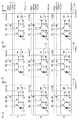
次に、本実施形態による撮像装置の駆動方法について、図3及び図4を用いて説明する。図3は、1フレーム期間における転送トランジスタM1,M2及びリセットトランジスタM3の動作を示すタイミングチャートである。図3には、連続する任意の3行分の駆動パルスを示している。図4は、1水平期間における信号の読み出し動作を示すタイミングチャートである。 Next, a method of driving the image pickup apparatus according to the present embodiment will be described with reference to FIGS. 3 and 4. FIG. 3 is a timing chart showing the operation of the transfer transistors M1 and M2 and the reset transistor M3 in one frame period. FIG. 3 shows drive pulses for any three consecutive rows. FIG. 4 is a timing chart showing a signal reading operation in one horizontal period.
図3中、制御信号PTX1は、転送トランジスタM1のゲートに供給される制御信号である。図3及び図4中、制御信号PTX2は、転送トランジスタM2のゲートに供給される制御信号である。図3及び図4中、制御信号PRESは、リセットトランジスタM3のゲートに供給される制御信号である。図4中、制御信号PSELは、選択トランジスタM5に供給される制御信号である。これら制御信号の符号に付記された(m−1),(m),(m+1)は、行番号を示している。 In FIG. 3, the control signal PTX1 is a control signal supplied to the gate of the transfer transistor M1. In FIGS. 3 and 4, the control signal PTX2 is a control signal supplied to the gate of the transfer transistor M2. In FIGS. 3 and 4, the control signal PRESS is a control signal supplied to the gate of the reset transistor M3. In FIG. 4, the control signal PSEL is a control signal supplied to the selection transistor M5. (M-1), (m), and (m + 1) added to the codes of these control signals indicate line numbers.
図3及び図4に示す各制御信号は、ハイレベルのときに対応するトランジスタがオンとなり、ローレベルのときに対応するトランジスタがオフとなる。各制御信号は、制御回路60による制御のもと垂直走査回路20から供給される。 In each of the control signals shown in FIGS. 3 and 4, the corresponding transistor is turned on at the high level, and the corresponding transistor is turned off at the low level. Each control signal is supplied from the
時刻T1より前の期間には、前フレームの蓄積動作が行われている。時刻T1の直前において、各行の制御信号PTX1はハイレベルであり、各行の制御信号PTX2,PRESはローレベルである。 In the period before the time T1, the accumulation operation of the previous frame is performed. Immediately before time T1, the control signal PTX1 of each line is at a high level, and the control signals PTX2 and PRESS of each line are at a low level.
時刻T1において、垂直走査回路20から総ての行の制御線TX1へと供給される制御信号PTX1をハイレベルからローレベルへと遷移し、総ての行の画素12の転送トランジスタM1をオフにする。これにより、前フレームの露光期間が終了する。前フレームの露光期間の間に各画素12の光電変換部Dで生成された電荷は、時刻T1には総て保持部C1へと転送されている。時刻T1は、前フレームの露光期間の終了時刻であり、次フレームの露光期間の開始時刻でもある。なお、制御信号PTX1は後述する時刻T10までローレベルとし、転送トランジスタM1をオフ状態のまま維持する。 At time T1, the control signal PTX1 supplied from the
時刻T1以降、前フレームの露光期間の間に各画素12の保持部C1に蓄積された電荷を、行単位で順次、保持部C1から保持部C2へと転送する。これにより、保持部C2に転送された電荷の量に応じた増幅部の入力ノード(増幅トランジスタM4のゲート)の電圧に基づく画素信号を、増幅トランジスタM4、選択トランジスタM5及び出力線16を介して、読み出し回路30に出力する。 After the time T1, the electric charges accumulated in the holding unit C1 of each
各行の読み出し動作は、例えば図4に示すタイミングチャートに従って実施する。図4の動作では、画素12の選択、リセット、ノイズ信号の読み出し(N読み)、保持部C1から保持部C2への電荷の転送、光信号の読み出し(S読み)、を順次行う。図3には、図4に示す制御信号のうち、制御信号PRES及び制御信号PTX2が示されている。図4には、第m−1行の画素12からの読み出しを行うときの時刻を記載している。 The read operation of each line is performed according to, for example, the timing chart shown in FIG. In the operation of FIG. 4,
ここで、図3に示す第m−1行の画素12からの読み出し動作を例にして、各行の読み出し動作を説明する。 Here, the read operation of each row will be described by taking the read operation from the
図示しない第m−2行の読み出し動作が完了した後の時刻T3において、垂直走査回路20から制御線SEL(m−1)へと供給される図示しない制御信号PSEL(m−1)がローレベルからハイレベルへと遷移する。これにより、第m−1行の画素12の選択トランジスタM5がオンになり、第m−1行目の画素12が選択状態となる。 At time T3 after the read operation of the m-2 line (not shown) is completed, the control signal PSEL (m-1) (not shown) supplied from the
次いで、時刻T4において、垂直走査回路20から制御線RES(m−1)へと供給される制御信号PRES(m−1)をローレベルからハイレベルへと遷移し、第m−1行目の画素12のリセットトランジスタM3をオンにする。これにより、第m−1行目の画素12の保持部C2を、電圧VRESに応じた所定の電圧にリセットする。 Then, at time T4, the control signal PRESS (m-1) supplied from the
次いで、制御信号PRES(m−1)をハイレベルからローレベルへと遷移した後、保持部C2のリセット電圧に基づく画素信号(ノイズ信号)を、増幅トランジスタM4、選択トランジスタM5及び出力線16を介して読み出し回路30に出力する(N読み)。 Next, after the control signal PRESS (m-1) is transitioned from the high level to the low level, the pixel signal (noise signal) based on the reset voltage of the holding unit C2 is transmitted to the amplification transistor M4, the selection transistor M5, and the
次いで、ノイズ信号を読み出した後の時刻T5において、垂直走査回路20から制御線TX2(m−1)へと供給される制御信号PTX2(m−1)をローレベルからハイレベルへと遷移する。これにより、転送トランジスタM2がオンとなり、第m−1行目の画素12の保持部C1に保持されていた電荷が保持部C2へと転送される。 Next, at time T5 after reading the noise signal, the control signal PTX2 (m-1) supplied from the
次いで、制御信号PTX2(m−1)をハイレベルからローレベルへと遷移した後、保持部C2に転送された電荷の量に基づく画素信号(光信号)を、増幅トランジスタM4、選択トランジスタM5及び出力線16を介して読み出し回路30に出力する(S読み)。なお、画素12からは、ノイズ信号を読み出さず、光信号のみを読み出すようにしてもよい。 Next, after the control signal PTX2 (m-1) is transitioned from the high level to the low level, the pixel signal (optical signal) based on the amount of electric charge transferred to the holding unit C2 is transferred to the amplification transistor M4, the selection transistor M5, and It is output to the
次いで、時刻T7において、制御信号PSEL(m−1)をハイレベルからローレベルへと遷移し、第m−1行の画素12の選択トランジスタM5をオフにして、第m−1行の画素12の選択を解除する。 Next, at time T7, the control signal PSEL (m-1) is transitioned from the high level to the low level, the selection transistor M5 of the
出力線16を介して画素12から出力されたアナログ信号は、出力回路50を介して撮像装置の外部へと出力される。画素12から読み出された信号は、撮像装置内(例えば読み出し回路30)においてAD変換処理を実施した後に出力してもよいし、アナログ信号として撮像装置の外部に出力した後にAD変換処理を実施してもよい。 The analog signal output from the
このようにして、総ての行について同様の読み出し動作を行い、前フレームの露光期間の間に蓄積された電荷に基づく画素信号を、行毎に順次、画素12から読み出し回路30へと出力する。 In this way, the same read operation is performed for all the rows, and the pixel signal based on the charge accumulated during the exposure period of the previous frame is sequentially output from the
総ての行の画素12の画素信号を読み出した後、時刻T9において、総ての行の制御信号PTX2及び制御信号PRESをローレベルからハイレベルと遷移し、転送トランジスタM2及びリセットトランジスタM3をオンにする。これにより、保持部C1を、転送トランジスタM2及びリセットトランジスタM3を介して、電圧VRESに応じた所定の電圧にリセットする。 After reading the pixel signals of the
次いで、総ての行の制御信号PTX2及び制御信号PRESをハイレベルからローレベルへと遷移して保持部C1のリセットを解除した後、時刻T10から時刻T11の期間において、総ての行の制御信号PTX1をローレベルからハイレベルへと遷移する。これにより、時刻T1から時刻T11の期間において光電変換部Dに蓄積された電荷を、光電変換部Dから保持部C1へと転送する。すなわち、光電変換部Dで生成された電荷は、時刻T1から時刻T10の期間においては光電変換部Dのみに蓄積され、時刻T10から時刻T11の期間においては光電変換部D及び保持部C1に蓄積されることになる。 Next, after the control signal PTX2 and the control signal PRESS of all the rows are changed from the high level to the low level and the reset of the holding unit C1 is released, the control of all the rows is controlled during the period from the time T10 to the time T11. The signal PTX1 transitions from low level to high level. As a result, the electric charge accumulated in the photoelectric conversion unit D during the period from the time T1 to the time T11 is transferred from the photoelectric conversion unit D to the holding unit C1. That is, the electric charge generated by the photoelectric conversion unit D is accumulated only in the photoelectric conversion unit D during the period from time T1 to time T10, and is accumulated in the photoelectric conversion unit D and the holding unit C1 during the period from time T10 to time T11. Will be done.
なお、保持部C1のリセットは、必ずしも時刻T9において全行同時に実施する必要はなく、読み出しの終了後、制御信号PTX1がハイレベルとなる時刻T10までの期間であれば、行毎に任意の期間に実施することができる(第3実施形態を参照)。保持部C1のリセットは、光電変換部Dから保持部C1に電荷を転送する時刻T10の直前に実施することが望ましい。 It should be noted that the reset of the holding unit C1 does not necessarily have to be performed at the same time for all lines at time T9, and is an arbitrary period for each line as long as it is a period from the end of reading to the time T10 when the control signal PTX1 becomes a high level. (See third embodiment). It is desirable that the reset of the holding unit C1 is performed immediately before the time T10 when the electric charge is transferred from the photoelectric conversion unit D to the holding unit C1.
このように、本実施形態の駆動方法では、保持部C1に保持されている電荷に基づく信号を読み出した後の時刻T9において、転送トランジスタM2及びリセットトランジスタM3をオンにして、保持部C2側から保持部C1を所定の電圧にリセットする。その後、光電変換部Dに蓄積されている電荷を保持部C1へと転送する。このようにして、光電変換部Dから保持部C1への電荷の転送前に保持部C1をリセットすることにより、例えば暗電流によって時刻T1から時刻T9の期間に保持部C1に発生したノイズ成分を排除することができ、より画質を向上することができる。 As described above, in the driving method of the present embodiment, the transfer transistor M2 and the reset transistor M3 are turned on at the time T9 after reading the signal based on the electric charge held in the holding unit C1, and the transfer transistor M2 and the reset transistor M3 are turned on from the holding unit C2 side. The holding unit C1 is reset to a predetermined voltage. After that, the electric charge accumulated in the photoelectric conversion unit D is transferred to the holding unit C1. In this way, by resetting the holding unit C1 before transferring the electric charge from the photoelectric conversion unit D to the holding unit C1, for example, the noise component generated in the holding unit C1 during the period from the time T1 to the time T9 due to the dark current is generated. It can be eliminated and the image quality can be further improved.
したがって、本実施形態によれば、グローバル電子シャッタ駆動においてノイズを抑制した良質な画像を取得することができる。 Therefore, according to the present embodiment, it is possible to acquire a high-quality image in which noise is suppressed in the global electronic shutter drive.
[第2実施形態]
本発明の第2実施形態による撮像装置及びその駆動方法について、図5乃至図8を用いて説明する。第1実施形態による撮像装置と同様の構成要素には同一の符号を付し、説明を省略し或いは簡潔にする。[Second Embodiment]
The image pickup apparatus according to the second embodiment of the present invention and the driving method thereof will be described with reference to FIGS. 5 to 8. The same components as those of the image pickup apparatus according to the first embodiment are designated by the same reference numerals, and the description thereof will be omitted or simplified.
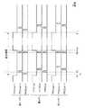
図5は、本実施形態による撮像装置の画素の構成例を示す回路図である。図6は、本実施形態による撮像装置の駆動方法を示すタイミングチャートである。図7は、本実施形態の変形例による撮像装置の駆動方法を示すタイミングチャートである。図8は、本実施形態による撮像装置の動作を模式的に示す図である。 FIG. 5 is a circuit diagram showing a configuration example of pixels of the image pickup apparatus according to the present embodiment. FIG. 6 is a timing chart showing a driving method of the image pickup apparatus according to the present embodiment. FIG. 7 is a timing chart showing a driving method of the image pickup apparatus according to a modified example of the present embodiment. FIG. 8 is a diagram schematically showing the operation of the image pickup apparatus according to the present embodiment.
はじめに、本実施形態による撮像装置の構成について、図5を用いて説明する。
本実施形態による撮像装置は、図5に示すように、各画素12が電荷排出トランジスタM6を更に有する点で、第1実施形態による撮像装置とは異なっている。First, the configuration of the image pickup apparatus according to the present embodiment will be described with reference to FIG.
As shown in FIG. 5, the image pickup apparatus according to the present embodiment is different from the image pickup apparatus according to the first embodiment in that each
電荷排出トランジスタM6のソースは、光電変換部Dを構成するフォトダイオードのカソードと転送トランジスタM1のソースとの接続ノードに接続されている。電荷排出トランジスタM6のドレインは、電源電圧線(VOFD)に接続されている。電荷排出トランジスタM6は、光電変換部Dに蓄積されている電荷をオーバーフロードレインなどの電源ノード(ここでは、電源電圧線VOFD)に排出する役割を有する。なお、電荷排出トランジスタM6のドレインに供給される電圧(VOFD)と電圧VDDや電圧VRESとは、同じであってもよいし、異なっていてもよい。 The source of the charge discharge transistor M6 is connected to a connection node between the cathode of the photodiode constituting the photoelectric conversion unit D and the source of the transfer transistor M1. The drain of the charge discharge transistor M6 is connected to the power supply voltage line (VOFD). The charge discharge transistor M6 has a role of discharging the charge accumulated in the photoelectric conversion unit D to a power supply node (here, power supply voltage line VOFD) such as an overflow drain. The voltage (VOFD) supplied to the drain of the charge discharge transistor M6 and the voltage VDD and the voltage VRES may be the same or different.
画素アレイ部10の画素アレイの各行に配された制御信号線14は、制御線OFGを更に含む。制御線OFGは、行方向に並ぶ画素12の電荷排出トランジスタM6のゲートにそれぞれ接続され、これら画素12に共通の信号線をなしている。制御線OFGは、垂直走査回路20に接続されている。制御線OFGには、垂直走査回路20から、電荷排出トランジスタM6を制御するための駆動パルスである制御信号POFGが出力される。典型例では、垂直走査回路20からハイレベルの制御信号POFGが出力されると対応する電荷排出トランジスタM6がオンとなり、垂直走査回路20からローレベルの制御信号POFGが出力されると対応する電荷排出トランジスタM6がオフとなる。 The
第1実施形態では、露光期間の開始時刻を、転送トランジスタM1をオンからオフに切り替えるタイミングによって制御する。これに対し、本実施形態のように光電変換部Dに接続して電荷排出トランジスタM6が設けられた画素構成では、電荷排出トランジスタM6の駆動タイミングによって露光期間の開始時刻や終了時刻を制御することも可能である。具体的には、電荷排出トランジスタM6がオンの期間に光電変換部Dで生成された電荷は排出され、電荷排出トランジスタM6がオフの期間に光電変換部Dで生成された電荷は蓄積される。したがって、電荷排出トランジスタM6の動作を制御することにより、露光期間の設定の自由度を向上することができる。 In the first embodiment, the start time of the exposure period is controlled by the timing of switching the transfer transistor M1 from on to off. On the other hand, in the pixel configuration in which the charge discharge transistor M6 is provided by connecting to the photoelectric conversion unit D as in the present embodiment, the start time and end time of the exposure period are controlled by the drive timing of the charge discharge transistor M6. Is also possible. Specifically, the charge generated by the photoelectric conversion unit D is discharged while the charge discharge transistor M6 is on, and the charge generated by the photoelectric conversion unit D is accumulated during the period when the charge discharge transistor M6 is off. Therefore, by controlling the operation of the charge discharge transistor M6, the degree of freedom in setting the exposure period can be improved.
次に、本実施形態による撮像装置の駆動方法について、図6を用いて説明する。図6は、1フレーム期間における電荷排出トランジスタM6、転送トランジスタM1,M2及びリセットトランジスタM3の動作を示すタイミングチャートである。 Next, a method of driving the image pickup apparatus according to the present embodiment will be described with reference to FIG. FIG. 6 is a timing chart showing the operations of the charge discharge transistors M6, the transfer transistors M1 and M2, and the reset transistor M3 in one frame period.
図6には、連続する任意の3行分の駆動パルスを示している。図6中、制御信号POFGは、電荷排出トランジスタM6のゲートに供給される制御信号である。図6に示す各制御信号は、ハイレベルのときに対応するトランジスタがオンとなり、ローレベルのときに対応するトランジスタがオフとなる。各制御信号は、制御回路60による制御のもと垂直走査回路20から供給される。 FIG. 6 shows drive pulses for any three consecutive rows. In FIG. 6, the control signal POFG is a control signal supplied to the gate of the charge discharge transistor M6. In each control signal shown in FIG. 6, the corresponding transistor is turned on at the high level, and the corresponding transistor is turned off at the low level. Each control signal is supplied from the
時刻T1より前の期間には、前フレームの蓄積動作が行われている。時刻T1の直前において、各行の制御信号PTX1はハイレベルであり、各行の制御信号POFG,PTX2,PRESはローレベルである。 In the period before the time T1, the accumulation operation of the previous frame is performed. Immediately before the time T1, the control signal PTX1 of each line is at a high level, and the control signals POFG, PTX2, and PRESS of each line are at a low level.
時刻T1において、垂直走査回路20から総ての行の制御線TX1へと供給される制御信号PTX1がハイレベルからローレベルへと遷移し、総ての行の画素12の転送トランジスタM1がオフになる。これにより、前フレームの露光期間が終了する。前フレームの露光期間の間に各画素12の光電変換部Dで生成された電荷は、時刻T1には総て保持部C1へと転送されている。時刻T1は、前フレームの露光期間の終了時刻である。 At time T1, the control signal PTX1 supplied from the
続く時刻T2において、垂直走査回路20から総ての行の制御線OFGへと供給される制御信号POFGをローレベルからハイレベルへと遷移し、総ての行の画素12の電荷排出トランジスタM6をオンにする。これにより、光電変換部Dに蓄積されていた電荷は、電荷排出トランジスタM6を介して排出される。制御信号POFGは、時刻T2から時刻T8までの期間、ハイレベルのままである。この期間の間に光電変換部Dで生成された電荷も、光電変換部Dには蓄積されず、電荷排出トランジスタM6を介して排出される。本実施形態では、制御信号POFGがローレベルとなる時刻T6から、光電変換部Dにおける電荷の蓄積が開始する。時刻T6が、次フレームの露光期間の開始時刻となる。 At the following time T2, the control signal POFG supplied from the
また、時刻T1以降、第1実施形態と同様にして、各行の画素12からの読み出し動作を行単位で順次実行する。 Further, after the time T1, the reading operation from the
総ての行の画素12から信号を読み出した後、時刻T9において、総ての行の制御信号PTX2及び制御信号PRESをローレベルからハイレベルと遷移し、転送トランジスタM2及びリセットトランジスタM3をオンにする。これにより、保持部C1を、転送トランジスタM2及びリセットトランジスタM3を介して、電圧VRESに応じた所定の電圧にリセットする。 After reading the signals from the
次いで、総ての行の制御信号PTX2及び制御信号PRESをハイレベルからローレベルへと遷移して保持部C1のリセットを解除した後、時刻T10から時刻T11の期間において、総ての行の制御信号PTX1をローレベルからハイレベルへと遷移する。これにより、時刻T8から時刻T11の期間において光電変換部Dに蓄積された電荷を、光電変換部Dから保持部C1へと転送する。すなわち、光電変換部Dで生成された電荷は、時刻T8から時刻T10の期間においては光電変換部Dのみに蓄積され、時刻T10から時刻T11の期間においては光電変換部D及び保持部C1に蓄積されることになる。時刻T11において制御信号PTX1がローレベルになることにより露光期間が終了し、時刻T8から時刻T11の期間に光電変換部Dで生成された電荷は、保持部C1にて保持されることになる。 Next, after the control signal PTX2 and the control signal PRESS of all the rows are changed from the high level to the low level and the reset of the holding unit C1 is released, the control of all the rows is controlled during the period from the time T10 to the time T11. The signal PTX1 transitions from low level to high level. As a result, the electric charge accumulated in the photoelectric conversion unit D during the period from time T8 to time T11 is transferred from the photoelectric conversion unit D to the holding unit C1. That is, the electric charge generated by the photoelectric conversion unit D is accumulated only in the photoelectric conversion unit D during the period from time T8 to time T10, and is accumulated in the photoelectric conversion unit D and the holding unit C1 during the period from time T10 to time T11. Will be done. When the control signal PTX1 becomes low level at time T11, the exposure period ends, and the electric charge generated by the photoelectric conversion unit D during the period from time T8 to time T11 is held by the holding unit C1.
なお、保持部C1のリセットは、必ずしも時刻T9において全行同時に実施する必要はなく、読み出しの終了後、制御信号PTX1がハイレベルとなる時刻T10までの期間であれば、行毎に任意の期間に実施することができる。保持部C1のリセットは、光電変換部Dから保持部C1に電荷を転送する時刻T10の直前に実施することが望ましい。 It should be noted that the reset of the holding unit C1 does not necessarily have to be performed at the same time for all lines at time T9, and is an arbitrary period for each line as long as it is a period from the end of reading to the time T10 when the control signal PTX1 becomes a high level. Can be carried out. It is desirable that the reset of the holding unit C1 is performed immediately before the time T10 when the electric charge is transferred from the photoelectric conversion unit D to the holding unit C1.
上述の駆動においてグローバル電子シャッタ動作を行う場合には、総ての行において少なくとも、制御信号POFGをローレベルにするタイミング(ここでは時刻T8)及び制御信号PTX1をローレベルにするタイミング(ここでは時刻T11)を同じにする。 When the global electronic shutter operation is performed in the above-mentioned drive, at least the timing of lowering the control signal POFG (here, time T8) and the timing of lowering the control signal PTX1 (here, time) in all the rows. Make T11) the same.
前述の通り、制御信号POFGがローレベルになるタイミング(ここでは時刻T8)は露光期間の開始時刻を規定するものであり、所望の露光期間に合わせて自由に設定することができる。また、制御信号POFGは、グローバル電子シャッタ動作を行う場合には、総ての行において同じタイミングで駆動される。そのため、図6における時刻T8、すなわち制御信号POFGがローレベルになるタイミングが、一部の行の画素12からの信号の読み出し期間と重なることも起こりうる。このような場合、制御信号POFGの駆動は全行同時であるため、画素アレイの規模によっては、制御信号POFGの駆動によって電源電圧や接地電圧等の電圧が変動し、読み出し中の画素12の信号に影響を与える可能性がある。そのため、制御信号POFGの立下りのタイミング(時刻T8)は、読み出し期間、例えばS読みのタイミング等のアナログ動作期間には実施しないように調整することが望ましい。 As described above, the timing at which the control signal POFG becomes low level (here, time T8) defines the start time of the exposure period, and can be freely set according to the desired exposure period. Further, the control signal POFG is driven at the same timing in all the rows when the global electronic shutter operation is performed. Therefore, the time T8 in FIG. 6, that is, the timing at which the control signal POFG becomes low level may overlap with the reading period of the signal from the
なお、図6に示す駆動例では、時刻T10から時刻T11の期間に制御信号PTX1をハイレベルのまま維持しているが、例えば図7に示す駆動例のように、制御信号PTX1を複数回に分けて駆動するようにしてもよい。この場合、制御信号PTX1がローレベルの期間には光電変換部Dにのみ電荷が蓄積され、制御信号PTX1がハイレベルの期間には光電変換部Dと保持部C1とに電荷が蓄積される。本駆動例においても、最初に制御信号PTX1がハイレベルとなるタイミング(時刻T10)よりも前の時刻T9において、保持部C1,C2が所定の電圧にリセットされればよい。 In the drive example shown in FIG. 6, the control signal PTX1 is maintained at a high level during the period from the time T10 to the time T11. However, as in the drive example shown in FIG. 7, the control signal PTX1 is set a plurality of times. It may be driven separately. In this case, the electric charge is accumulated only in the photoelectric conversion unit D during the low level period of the control signal PTX1, and the electric charge is accumulated in the photoelectric conversion unit D and the holding unit C1 during the high level period of the control signal PTX1. Also in this drive example, the holding units C1 and C2 may be reset to a predetermined voltage at a time T9 before the timing (time T10) when the control signal PTX1 first becomes a high level.
このように、本実施形態の駆動方法では、保持部C1に保持されている電荷に基づく信号を読み出した後の時刻T9において、転送トランジスタM2及びリセットトランジスタM3をオンにして、保持部C2側から保持部C1を所定の電圧にリセットする。その後、光電変換部Dに蓄積されている電荷を保持部C1へと転送する。このようにして、光電変換部Dから保持部C1への電荷の転送前に保持部C1をリセットすることにより、例えば暗電流によって時刻T8から時刻T9の期間に保持部C1に発生したノイズ成分を排除することができ、より画質を向上することができる。 As described above, in the driving method of the present embodiment, the transfer transistor M2 and the reset transistor M3 are turned on at the time T9 after reading the signal based on the electric charge held in the holding unit C1, and the transfer transistor M2 and the reset transistor M3 are turned on from the holding unit C2 side. The holding unit C1 is reset to a predetermined voltage. After that, the electric charge accumulated in the photoelectric conversion unit D is transferred to the holding unit C1. In this way, by resetting the holding unit C1 before transferring the electric charge from the photoelectric conversion unit D to the holding unit C1, for example, the noise component generated in the holding unit C1 during the period from time T8 to time T9 due to the dark current is generated. It can be eliminated and the image quality can be further improved.
したがって、本実施形態によれば、グローバル電子シャッタ駆動においてノイズを抑制した良質な画像を取得することができる。 Therefore, according to the present embodiment, it is possible to acquire a high-quality image in which noise is suppressed in the global electronic shutter drive.
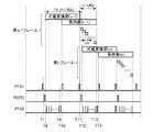
本実施形態による撮像装置のより具体的な動作について、図8を用いて説明する。図8には、第n−1フレーム及び第nフレームにおける動作の概略を示している。図6及び図7の時刻T1〜時刻T11に対応する時刻には、図8においても同一の符号を付している。なお、ここでは1秒間に60フレームの画像を取得する動作(フレームレートが1/60秒)を想定して説明を行うが、フレームレートは特に限定されるものではない。 A more specific operation of the image pickup apparatus according to the present embodiment will be described with reference to FIG. FIG. 8 shows an outline of the operation in the n-1th frame and the nth frame. The times corresponding to the times T1 to T11 in FIGS. 6 and 7 are designated by the same reference numerals in FIG. Here, the description is made assuming an operation of acquiring an image of 60 frames per second (frame rate is 1/60 second), but the frame rate is not particularly limited.
時刻T8において制御信号POFGがハイレベルからローレベルへと制御されることにより、全行同時に光電変換部Dのリセットが解除され、第n−1フレームにおける電荷の蓄積が開始する。また、時刻T12において制御信号POFGがハイレベルからローレベルへと制御されることにより、全行同時に光電変換部Dのリセットが解除され、第nフレームにおける電荷の蓄積が開始する。本実施形態では、時刻T8から時刻T12までの期間が、1フレーム期間に対応する1/60秒となる。 By controlling the control signal POFG from the high level to the low level at time T8, the reset of the photoelectric conversion unit D is released at the same time for all lines, and the charge accumulation in the n-1th frame starts. Further, by controlling the control signal POFG from the high level to the low level at time T12, the reset of the photoelectric conversion unit D is released at the same time for all the lines, and the charge accumulation in the nth frame starts. In the present embodiment, the period from time T8 to time T12 is 1/60 second corresponding to one frame period.
光電変換部Dから保持部C1に電荷を転送するタイミングよりも前の時刻T9に、図示しない制御信号PRESとともに制御信号PTX2をローレベルからハイレベルへと遷移し、保持部C1をリセットする。 At time T9, which is before the timing of transferring the electric charge from the photoelectric conversion unit D to the holding unit C1, the control signal PTX2 is changed from the low level to the high level together with the control signal PRESS (not shown), and the holding unit C1 is reset.
光電変換部Dから保持部C1への電荷の転送は、時刻T10において立ち上がる制御信号PTX1の駆動パルスのタイミングと、時刻T11に立ち下がる制御信号PTX1の駆動パルスのタイミングとにおいて行われる。本駆動例は、図7のタイミングチャートにおいて、時刻T10から時刻T11の間に制御信号PTX1を2回に分けて駆動する場合に相当する。 The transfer of electric charge from the photoelectric conversion unit D to the holding unit C1 is performed at the timing of the drive pulse of the control signal PTX1 rising at time T10 and the timing of the drive pulse of the control signal PTX1 falling at time T11. This drive example corresponds to the case where the control signal PTX1 is driven in two steps between the time T10 and the time T11 in the timing chart of FIG.
第n−1フレームにおいて光電変換部Dで生成された電荷は、時刻T8から時刻T11の期間においては光電変換部Dに蓄積され、時刻T10から時刻T13の期間においては保持部C1に蓄積される。光電変換部Dで生成された電荷は、時刻T10から時刻T11の期間には、光電変換部D及び保持部C1に蓄積されることになる。なお、時刻T13は、第n−1フレームの時刻T9に対応する第nフレームの時刻である。 The electric charge generated by the photoelectric conversion unit D in the n-1th frame is accumulated in the photoelectric conversion unit D during the period from time T8 to time T11, and is accumulated in the holding unit C1 during the period from time T10 to time T13. .. The electric charge generated by the photoelectric conversion unit D will be accumulated in the photoelectric conversion unit D and the holding unit C1 during the period from the time T10 to the time T11. The time T13 is the time of the nth frame corresponding to the time T9 of the n-1th frame.
本駆動例では、時刻T10において立ち上がる制御信号PTX1の駆動パルスのタイミングを、時刻T8と時刻T11との間隔で決まる露光期間の中間付近に設定している。時刻T8から時刻T10までの期間に光電変換部Dに蓄積していた電荷は時刻T10に保持部C1へと転送するため、光電変換部Dに蓄積可能な電荷の量(飽和電荷量)は、画素12の飽和電荷量、すなわち保持部C1の飽和電荷量のおよそ半分でよい。 In this drive example, the timing of the drive pulse of the control signal PTX1 that rises at time T10 is set near the middle of the exposure period determined by the interval between time T8 and time T11. Since the electric charge accumulated in the photoelectric conversion unit D during the period from time T8 to time T10 is transferred to the holding unit C1 at time T10, the amount of charge that can be accumulated in the photoelectric conversion unit D (saturated charge amount) is determined. The saturated charge amount of the
したがって、本構成を適用することで、光電変換部Dの面積は保持部C1の面積のおよそ半分にすることができ、画素12の面積を縮小することが可能になる。時刻T8から時刻T10までの期間を時刻T10から時刻T11までの期間よりも短くすれば、光電変換部Dの飽和電荷量を更に小さくすることも可能である。なお、時刻T3から時刻T4までの期間においては、例えば図6に示す駆動例のように、制御信号PTX1をハイレベルに固定してもよい。 Therefore, by applying this configuration, the area of the photoelectric conversion unit D can be reduced to about half the area of the holding unit C1, and the area of the
時刻T12以降、光電変換部Dでは、第nフレームの蓄積動作を開始する。光電変換部Dで生成された電荷は、次に制御信号PTX1がハイレベルとなる時刻T14までは、光電変換部Dのみに蓄積される。 After time T12, the photoelectric conversion unit D starts the accumulation operation of the nth frame. The electric charge generated by the photoelectric conversion unit D is accumulated only in the photoelectric conversion unit D until the time T14 when the control signal PTX1 becomes the next high level.
時刻T11から時刻T13までの期間には、制御信号PTX2を制御し、第n−1フレームの信号を行毎に順次読み出す。第n−1フレームの信号の読み出し期間は、第nフレームの電荷を光電変換部Dのみで蓄積している期間であり、本駆動例では1フレーム期間の半分、つまり1/120秒となる。全行の信号読み出し動作が完了したのち、時刻T13において保持部C1のリセットを実施し、時刻T14において制御信号PTX1をハイレベルにすることにより、第nフレームの電荷を保持部C1へと転送する。 During the period from time T11 to time T13, the control signal PTX2 is controlled, and the signal of the n-1th frame is sequentially read line by line. The read-out period of the signal of the n-1th frame is a period in which the charge of the nth frame is accumulated only by the photoelectric conversion unit D, and in this driving example, it is half of the one-frame period, that is, 1/120 second. After the signal reading operation of all lines is completed, the holding unit C1 is reset at time T13, and the control signal PTX1 is set to a high level at time T14 to transfer the charge of the nth frame to the holding unit C1. ..
このようにして、保持部C1への電荷の転送回数及び読み出し時間を制御することで、画素12の飽和電荷量を向上しつつ、レイアウト面積を最小化することができる。保持部C1のリセット動作は、光電変換部Dから保持部C1へと電荷の転送を行う最初のタイミングよりも前、つまり本駆動例では時刻T10よりも前の時刻T9に実施すればよい。 By controlling the number of charge transfers to the holding unit C1 and the read time in this way, the layout area can be minimized while improving the saturated charge amount of the
[第3実施形態]
本発明の第3実施形態による撮像装置及びその駆動方法について、図9乃至図11を用いて説明する。第1及び第2実施形態による撮像装置と同様の構成要素には同一の符号を付し、説明を省略し或いは簡潔にする。[Third Embodiment]
The image pickup apparatus according to the third embodiment of the present invention and the driving method thereof will be described with reference to FIGS. 9 to 11. The same components as those of the image pickup apparatus according to the first and second embodiments are designated by the same reference numerals, and the description thereof will be omitted or simplified.
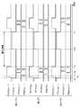
図9及び図10は、本実施形態による撮像装置の駆動方法を示すタイミングチャートである。図11は、本実施形態の変形例による撮像装置の駆動方法を示すタイミングチャートである。 9 and 10 are timing charts showing a method of driving the image pickup apparatus according to the present embodiment. FIG. 11 is a timing chart showing a driving method of the image pickup apparatus according to a modified example of the present embodiment.
本実施形態では、第2実施形態による撮像装置の他の駆動方法を説明する。本実施形態による撮像装置の駆動方法は、保持部C1のリセットを行うタイミングが、第2実施形態による撮像装置の駆動方法とは異なっている。 In this embodiment, another driving method of the image pickup apparatus according to the second embodiment will be described. In the driving method of the imaging device according to the present embodiment, the timing of resetting the holding unit C1 is different from the driving method of the imaging device according to the second embodiment.
すなわち、本実施形態の駆動方法は、図9に示すように、制御信号PTX2及び制御信号PRESにより実施される保持部C1のリセット動作を、行毎に、信号読み出し動作の終了後に実施している点で、第2実施形態の駆動方法とは異なっている。 That is, in the driving method of the present embodiment, as shown in FIG. 9, the reset operation of the holding unit C1 executed by the control signal PTX2 and the control signal PRESS is performed row by line after the signal reading operation is completed. In that respect, it differs from the driving method of the second embodiment.
本実施形態の駆動方法では、各行の読み出し動作を、例えば図10に示すタイミングチャートに従って実施する。図10中、制御信号PSELは、選択トランジスタM5に供給される制御信号である。制御信号PRESは、リセットトランジスタM3に供給される制御信号である。制御信号PTX2は、転送トランジスタM2に供給される制御信号である。図10の動作では、画素12の選択、リセット、ノイズ信号の読み出し(N読み)、保持部C1から保持部C2への電荷の転送、光信号の読み出し(S読み)、保持部C1のリセット、を順次行う。つまり、本実施形態の駆動方法では、1水平期間の間に、信号の読み出しと、保持部C1のリセットとを行う。 In the driving method of the present embodiment, the reading operation of each line is performed according to, for example, the timing chart shown in FIG. In FIG. 10, the control signal PSEL is a control signal supplied to the selection transistor M5. The control signal PRESS is a control signal supplied to the reset transistor M3. The control signal PTX2 is a control signal supplied to the transfer transistor M2. In the operation of FIG. 10,
このように、本実施形態の駆動方法では、図4に示した読み出し動作と同様にして光信号を読み出した後、時刻T7において画素12の選択を解除する前に、時刻T6において、保持部C2を介して保持部C1のリセットを行う。時刻T6において行う保持部C1のリセット動作は、全行一括ではなく選択行の画素12に対してのみ行う点を除き、第2実施形態の駆動方法で時刻T9において行う保持部C1のリセット動作と同様である。 As described above, in the driving method of the present embodiment, after reading the optical signal in the same manner as the reading operation shown in FIG. 4, before deselecting the
上記動作により、総ての行に対して信号の読み出し動作及び保持部C1のリセットを順次行った後、第2実施形態と同様にして、時刻T8以降の信号の蓄積動作を開始する。 By the above operation, the signal reading operation and the reset of the holding unit C1 are sequentially performed for all the rows, and then the signal accumulating operation after the time T8 is started in the same manner as in the second embodiment.
本実施形態の駆動方法においても、第2実施形態の場合と同様、例えば図11に示すように、時刻T10から時刻T11の期間に、制御信号PTX1を複数回に分けて駆動するようにしてもよい。この場合、制御信号PTX1がローレベルの期間には光電変換部Dにのみ電荷が蓄積され、制御信号PTX1がハイレベルの期間には光電変換部Dと保持部C1とに電荷が蓄積される。本駆動例においても、最初に制御信号PTX1がハイレベルとなるタイミング(時刻T10)よりも前の時刻T6において、保持部C1,C2が所定の電圧にリセットされればよい。 Also in the driving method of the present embodiment, as in the case of the second embodiment, for example, as shown in FIG. 11, the control signal PTX1 may be driven in a plurality of times during the period from the time T10 to the time T11. Good. In this case, the electric charge is accumulated only in the photoelectric conversion unit D during the low level period of the control signal PTX1, and the electric charge is accumulated in the photoelectric conversion unit D and the holding unit C1 during the high level period of the control signal PTX1. Also in this drive example, the holding units C1 and C2 may be reset to a predetermined voltage at a time T6 before the timing (time T10) when the control signal PTX1 first becomes a high level.
本実施形態の駆動方法によれば、各行で、保持部C1をリセットしてから、制御信号PTX2を駆動して保持部C1から信号を読み出すまでの期間がほぼ等しくなる。そのため、保持部C1において例えば暗電流等のノイズが発生した場合においても、その発生量が各行でほぼ等しくなり、画面内でムラが発生するのを抑制できる。 According to the driving method of the present embodiment, the period from resetting the holding unit C1 to driving the control signal PTX2 and reading the signal from the holding unit C1 is substantially equal in each line. Therefore, even when noise such as a dark current is generated in the holding unit C1, the amount of noise generated is substantially equal in each row, and it is possible to suppress the occurrence of unevenness in the screen.
このように、本実施形態によれば、グローバル電子シャッタ駆動においてノイズやムラを抑制した良質な画像を取得することができる。 As described above, according to the present embodiment, it is possible to acquire a high-quality image in which noise and unevenness are suppressed in the global electronic shutter drive.
[第4実施形態]
本発明の第4実施形態による撮像システムについて、図12を用いて説明する。第1乃至第3実施形態による撮像装置と同様の構成要素には同一の符号を付し説明を省略し或いは簡潔にする。図12は、本実施形態による撮像システムの構成を示すブロック図である。[Fourth Embodiment]
The imaging system according to the fourth embodiment of the present invention will be described with reference to FIG. The same components as those of the image pickup apparatus according to the first to third embodiments are designated by the same reference numerals, and the description thereof will be omitted or simplified. FIG. 12 is a block diagram showing a configuration of an imaging system according to the present embodiment.
上記第1乃至第3実施形態で述べた撮像装置100は、種々の撮像システムに適用可能である。適用可能な撮像システムの例としては、デジタルスチルカメラ、デジタルカムコーダ、監視カメラ、複写機、ファックス、携帯電話、車載カメラ、観測衛星などが挙げられる。また、レンズなどの光学系と撮像装置とを備えるカメラモジュールも、撮像システムに含まれる。図12には、これらのうちの一例として、デジタルスチルカメラのブロック図を例示している。 The
図12に例示した撮像システム200は、撮像装置100、被写体の光学像を撮像装置100に結像させるレンズ202、レンズ202を通過する光量を可変にするための絞り204、レンズ202の保護のためのバリア206を有する。レンズ202及び絞り204は、撮像装置100に光を集光する光学系である。撮像装置100は、第1乃至第5実施形態で説明した撮像装置100であって、レンズ202により結像された光学像を画像データに変換する。 The
撮像システム200は、また、撮像装置100より出力される出力信号の処理を行う信号処理部208を有する。信号処理部208は、撮像装置100が出力するアナログ信号をデジタル信号に変換するAD変換を行う。また、信号処理部208はその他、必要に応じて各種の補正、圧縮を行って画像データを出力する動作を行う。信号処理部208の一部であるAD変換部は、撮像装置100が設けられた半導体基板に形成されていてもよいし、撮像装置100とは別の半導体基板に形成されていてもよい。また、撮像装置100と信号処理部208とが同一の半導体基板に形成されていてもよい。 The
撮像システム200は、さらに、画像データを一時的に記憶するためのメモリ部210、外部コンピュータ等と通信するための外部インターフェース部(外部I/F部)212を有する。さらに撮像システム200は、撮像データの記録又は読み出しを行うための半導体メモリ等の記録媒体214、記録媒体214に記録又は読み出しを行うための記録媒体制御インターフェース部(記録媒体制御I/F部)216を有する。なお、記録媒体214は、撮像システム200に内蔵されていてもよく、着脱可能であってもよい。 The
さらに撮像システム200は、各種演算とデジタルスチルカメラ全体を制御する全体制御・演算部218、撮像装置100と信号処理部208に各種タイミング信号を出力するタイミング発生部220を有する。ここで、タイミング信号などは外部から入力されてもよく、撮像システム200は少なくとも撮像装置100と、撮像装置100から出力された出力信号を処理する信号処理部208とを有すればよい。 Further, the
撮像装置100は、撮像信号を信号処理部208に出力する。信号処理部208は、撮像装置100から出力される撮像信号に対して所定の信号処理を実施し、画像データを出力する。信号処理部208は、撮像信号を用いて、画像を生成する。 The
第1乃至第3実施形態による撮像装置100を適用することにより、グローバル電子シャッタ駆動においてノイズやムラの少ない良質な画像を取得しうる撮像システムを実現することができる。 By applying the
[第5実施形態]
本発明の第5実施形態による撮像システム及び移動体について、図13を用いて説明する。図13は、本実施形態による撮像システム及び移動体の構成を示す図である。[Fifth Embodiment]
The imaging system and the moving body according to the fifth embodiment of the present invention will be described with reference to FIG. FIG. 13 is a diagram showing a configuration of an imaging system and a moving body according to the present embodiment.
図13(a)は、車戴カメラに関する撮像システムの一例を示したものである。撮像システム300は、撮像装置310を有する。撮像装置310は、上記第1乃至第3実施形態のいずれかに記載の撮像装置100である。撮像システム300は、撮像装置310により取得された複数の画像データに対し、画像処理を行う画像処理部312と、撮像システム300により取得された複数の画像データから視差(視差画像の位相差)の算出を行う視差算出部314を有する。また、撮像システム300は、算出された視差に基づいて対象物までの距離を算出する距離計測部316と、算出された距離に基づいて衝突可能性があるか否かを判定する衝突判定部318と、を有する。ここで、視差算出部314や距離計測部316は、対象物までの距離情報を取得する距離情報取得手段の一例である。すなわち、距離情報とは、視差、デフォーカス量、対象物までの距離等に関する情報である。衝突判定部318はこれらの距離情報のいずれかを用いて、衝突可能性を判定してもよい。距離情報取得手段は、専用に設計されたハードウェアによって実現されてもよいし、ソフトウェアモジュールによって実現されてもよい。また、FPGA(Field Programmable Gate Array)やASIC(Application Specific Integrated circuit)等によって実現されてもよいし、これらの組合せによって実現されてもよい。 FIG. 13A shows an example of an imaging system related to a vehicle-mounted camera. The
撮像システム300は車両情報取得装置320と接続されており、車速、ヨーレート、舵角などの車両情報を取得することができる。また、撮像システム300は、衝突判定部318での判定結果に基づいて、車両に対して制動力を発生させる制御信号を出力する制御装置である制御ECU330が接続されている。また、撮像システム300は、衝突判定部318での判定結果に基づいて、ドライバーへ警報を発する警報装置340とも接続されている。例えば、衝突判定部318の判定結果として衝突可能性が高い場合、制御ECU330はブレーキをかける、アクセルを戻す、エンジン出力を抑制するなどして衝突を回避、被害を軽減する車両制御を行う。警報装置340は音等の警報を鳴らす、カーナビゲーションシステムなどの画面に警報情報を表示する、シートベルトやステアリングに振動を与えるなどしてユーザに警告を行う。 The
本実施形態では、車両の周囲、例えば前方又は後方を撮像システム300で撮像する。図13(b)に、車両前方(撮像範囲350)を撮像する場合の撮像システムを示した。車両情報取得装置320が、上述の第1乃至第3の実施形態に記載した動作を行うように撮像システム300ないしは撮像装置310に指示を送る。撮像装置310の動作は、第1乃至第3の実施形態と同じなので、ここでは説明を省略する。このような構成により、測距の精度をより向上させることができる。 In the present embodiment, the periphery of the vehicle, for example, the front or the rear, is imaged by the
上記では、他の車両と衝突しないように制御する例を説明したが、他の車両に追従して自動運転する制御や、車線からはみ出さないように自動運転する制御などにも適用可能である。さらに、撮像システムは、自車両等の車両に限らず、例えば、船舶、航空機あるいは産業用ロボットなどの移動体(移動装置)に適用することができる。加えて、移動体に限らず、高度道路交通システム(ITS)等、広く物体認識を利用する機器に適用することができる。 In the above, an example of controlling so as not to collide with another vehicle has been described, but it can also be applied to control for automatically driving following other vehicles and control for automatically driving so as not to go out of the lane. .. Further, the imaging system can be applied not only to a vehicle such as a own vehicle but also to a moving body (moving device) such as a ship, an aircraft, or an industrial robot. In addition, it can be applied not only to mobile objects but also to devices that widely use object recognition, such as intelligent transportation systems (ITS).
[変形実施形態]
本発明は、上記実施形態に限らず種々の変形が可能である。[Modification Embodiment]
The present invention is not limited to the above embodiment, and various modifications are possible.
例えば、いずれかの実施形態の一部の構成を他の実施形態に追加した例や、他の実施形態の一部の構成と置換した例も、本発明の実施形態である。 For example, an example in which a part of the configuration of any of the embodiments is added to another embodiment or an example in which a part of the configuration of another embodiment is replaced with another embodiment is also an embodiment of the present invention.
また、上記実施形態では、撮像装置をグローバル電子シャッタ駆動する場合について述べたが、本発明は撮像装置をローリング電子シャッタ駆動する場合においても同様に適用可能である。 Further, in the above embodiment, the case where the image pickup apparatus is driven by the global electronic shutter has been described, but the present invention can be similarly applied to the case where the image pickup apparatus is driven by the rolling electronic shutter.
また、上記実施形態では、画素アレイの総ての行の画素から信号を読み出す場合を例にして説明したが、必ずしも総ての行の総ての画素から信号を読み出す必要はない。画素アレイから出力する信号の数は、出力する画像のフォーマットによって変更されうる。例えば動画の撮影であれば、1フレームに用いられる水平ラインの数だけ信号が出力されればよい。このような実施形態では、撮像装置が備える画素の全部から信号が出力されなくてもよい。 Further, in the above embodiment, the case where the signal is read from the pixels in all the rows of the pixel array has been described as an example, but it is not always necessary to read the signal from all the pixels in all the rows. The number of signals output from the pixel array can be changed depending on the format of the output image. For example, when shooting a moving image, signals may be output as many as the number of horizontal lines used in one frame. In such an embodiment, the signal may not be output from all the pixels included in the image pickup apparatus.
また、第4及び第5実施形態に示した撮像システムは、本発明の撮像装置を適用しうる撮像システム例を示したものであり、本発明の撮像装置を適用可能な撮像システムは図12及び図13に示した構成に限定されるものではない。 Further, the imaging systems shown in the fourth and fifth embodiments show an example of an imaging system to which the imaging apparatus of the present invention can be applied, and the imaging systems to which the imaging apparatus of the present invention can be applied are shown in FIGS. The configuration is not limited to the configuration shown in FIG.
なお、上記実施形態は、何れも本発明を実施するにあたっての具体化の例を示したものに過ぎず、これらによって本発明の技術的範囲が限定的に解釈されてはならないものである。すなわち、本発明はその技術思想、又はその主要な特徴から逸脱することなく、様々な形で実施することができる。 It should be noted that all of the above embodiments merely show examples of embodiment in carrying out the present invention, and the technical scope of the present invention should not be construed in a limited manner by these. That is, the present invention can be implemented in various forms without departing from the technical idea or its main features.
D…光電変換部
M1,M2…転送トランジスタ
M3…リセットトランジスタ
M4…増幅トランジスタ
M5…選択トランジスタ
M6…電荷排出トランジスタ
12…画素
20…垂直走査回路
30…読み出し回路
40…水平走査回路
50…出力回路
60…制御回路
100…撮像装置D ... Photoelectric conversion unit M1, M2 ... Transfer transistor M3 ... Reset transistor M4 ... Amplification transistor M5 ... Selective transistor M6 ...
Claims (11)
Translated fromJapanese前記複数の画素のそれぞれは、第1の期間に前記光電変換部が前記電荷を保持し、前記第1の期間の後の第2の期間に、前記電荷を前記光電変換部から前記保持部に転送するように構成され、
前記保持部に転送された前記電荷の読み出しが前記第1行で行われた後、前記第2行で行われ、
前記リセット部による前記保持部のリセットが前記第1行で行われた後、前記第2行で行われるように更に構成されている
ことを特徴とする撮像装置。A photoelectric conversion unit that generates an electric charge by photoelectric conversion, a holding unit that holds the electric charge transferred from the photoelectric conversion unit, an amplification unit that outputs a signal based on the electric charge transferred from the holding unit, and areset unit. , Each of which has a plurality of pixelsare arranged over a plurality of rows including the first row and the second row .
Wherein each of the plurality of pixels, the photoelectric conversion unitin the firstperiodto hold the charge,the second period following said first period, before Symbol the holding unit chargefrom the photoelectric conversion portionConfigured to transfer to
The reading of the charge transferred to the holding unit is performed in the first line, and then in the second line.
An image pickup apparatus characterized in that thereset portion is further configured tobe reset in the first row and then in the second row .
前記露光期間の終了は、前記複数の画素で同時である
ことを特徴とする請求項1に記載の撮像装置。The start of the exposure period issimultaneous for the plurality of pixels,
The imaging apparatus according to claim 1, wherein the end of the exposure period is simultaneous for theplurality of pixels .
ことを特徴とする請求項1または2に記載の撮像装置。Each of the plurality of pixels, a first transfer transistor for transferring charges of the photoelectric conversion unit to the holding portion, that the charge of the holding portionand a second transfer transistor for transferring to the amplifying section The imaging apparatus according to claim 1 or 2.
ことを特徴とする請求項3記載の撮像装置。The reset unit is connected to the reset transistor to the amplifying unit, a reset of thepre-Symbol holding portion, wherein said reset transistor, and the amplifier unit, to be implemented through the second transfer transistor The imaging device according to claim 3.
ことを特徴とする請求項3又は4記載の撮像装置。The imaging apparatus according to claim 3 or 4, wherein the first transfer transistor is maintained in an off state during the first period.
ことを特徴とする請求項3乃至5のいずれか1項に記載の撮像装置。The imaging apparatus according to any one of claims 3 to 5, wherein the first transfer transistor is turned on a plurality of times during the second period.
露光期間の開始時刻は、前記電荷排出トランジスタをオフにするタイミングによって規定されている
ことを特徴とする請求項1乃至6のいずれか1項に記載の撮像装置。Each of the plurality of pixels further has a charge discharge transistor for discharging the charge of the photoelectric conversion unit.
Start time of theexposure light period, the imaging apparatus according to any one of claims 1 to 6, characterized in that it is defined by the timing for turning off the charge discharging transistor.
前記光電変換部が前記電荷を保持する第1の期間と、前記第1の期間の後の期間であって、前記電荷を前記光電変換部から前記保持部に転送する第2の期間と、を含む露光期間の間に前記光電変換部で生じた電荷に基づく信号を出力する撮像装置の駆動方法であって、
前記保持部に転送された前記電荷の読み出しが前記第1行で行われた後、前記第2行で行われ、
前記リセット部による前記保持部のリセットが前記第1行で行われた後、前記第2行で行われる
ことを特徴とする撮像装置の駆動方法。A photoelectric conversion unit that generates an electric charge by photoelectric conversion, a holding unit that holds the electric charge transferred from the photoelectric conversion unit, an amplification unit that outputs a signal based on the electric charge transferred from the holding unit, and areset unit. , Each of which has a plurality of pixelsare arranged over a plurality of rows including the first row and the second row .
A first period in which the photoelectric conversion unittohold the charge,a period after the first period, a second period fortransferringpre Symbol chargein the holding portionfrom the photoelectric conversion portion A method of driving an image pickup apparatus that outputs a signal based on the electric charge generated in the photoelectric conversion unit during an exposure period including.
The reading of the charge transferred to the holding unit is performed in the first line, and then in the second line.
A method for driving an imaging device,which comprises resetting the holding portion by the reset portion in the first row and then in the second row .
前記露光期間の終了は、前記複数の画素で同時である
ことを特徴とする請求項8に記載の撮像装置の駆動方法。The start of the exposure period is simultaneous for the plurality of pixels,
The method for driving an imaging device according to claim 8, wherein the end of the exposure period is simultaneous for the plurality of pixels.
前記撮像装置の前記画素から出力される前記信号を処理する信号処理部と
を有することを特徴とする撮像システム。The imaging device according to any one of claims 1 to 7.
An imaging system characterized by having a signal processing unit that processes the signal output from the pixel of the imaging device.
請求項1乃至7のいずれか1項に記載の撮像装置と、
前記撮像装置からの信号に基づく視差画像から、対象物までの距離情報を取得する距離情報取得手段と、
前記距離情報に基づいて前記移動体を制御する制御手段と
を有することを特徴とする移動体。It ’s a mobile body,
The imaging device according to any one of claims 1 to 7.
A distance information acquisition means for acquiring distance information to an object from a parallax image based on a signal from the imaging device, and
A moving body having a control means for controlling the moving body based on the distance information.
Priority Applications (2)
| Application Number | Priority Date | Filing Date | Title |
|---|---|---|---|
| JP2016243111AJP6806553B2 (en) | 2016-12-15 | 2016-12-15 | Imaging device, driving method of imaging device and imaging system |
| US15/824,053US10249678B2 (en) | 2016-12-15 | 2017-11-28 | Imaging device, method of driving imaging device, and imaging system |
Applications Claiming Priority (1)
| Application Number | Priority Date | Filing Date | Title |
|---|---|---|---|
| JP2016243111AJP6806553B2 (en) | 2016-12-15 | 2016-12-15 | Imaging device, driving method of imaging device and imaging system |
Publications (2)
| Publication Number | Publication Date |
|---|---|
| JP2018098690A JP2018098690A (en) | 2018-06-21 |
| JP6806553B2true JP6806553B2 (en) | 2021-01-06 |
Family
ID=62562646
Family Applications (1)
| Application Number | Title | Priority Date | Filing Date |
|---|---|---|---|
| JP2016243111AActiveJP6806553B2 (en) | 2016-12-15 | 2016-12-15 | Imaging device, driving method of imaging device and imaging system |
Country Status (2)
| Country | Link |
|---|---|
| US (1) | US10249678B2 (en) |
| JP (1) | JP6806553B2 (en) |
Families Citing this family (9)
| Publication number | Priority date | Publication date | Assignee | Title |
|---|---|---|---|---|
| JP6806553B2 (en)* | 2016-12-15 | 2021-01-06 | キヤノン株式会社 | Imaging device, driving method of imaging device and imaging system |
| JP2019029693A (en)* | 2017-07-25 | 2019-02-21 | キヤノン株式会社 | Imaging device, imaging system, moving object |
| JP7150469B2 (en)* | 2018-05-17 | 2022-10-11 | キヤノン株式会社 | Imaging device and imaging system |
| US10834354B2 (en) | 2018-06-25 | 2020-11-10 | Canon Kabushiki Kaisha | Imaging device, imaging system, movable object, and signal processing device |
| DE112020001187T5 (en)* | 2019-03-11 | 2022-03-17 | Sony Semiconductor Solutions Corporation | IMAGING ELEMENT AND IMAGING DEVICE |
| JP7614742B2 (en) | 2020-05-28 | 2025-01-16 | キヤノン株式会社 | Photoelectric conversion device, photoelectric conversion system, mobile object, and signal processing method |
| JP7649152B2 (en) | 2021-02-04 | 2025-03-19 | キヤノン株式会社 | Photoelectric conversion device and electronic device |
| JP2023042891A (en) | 2021-09-15 | 2023-03-28 | キヤノン株式会社 | Photoelectric conversion device and method of driving the same |
| JP2024073685A (en) | 2022-11-18 | 2024-05-30 | キヤノン株式会社 | Photoelectric conversion device and driving method thereof |
Family Cites Families (35)
| Publication number | Priority date | Publication date | Assignee | Title |
|---|---|---|---|---|
| TW421962B (en) | 1997-09-29 | 2001-02-11 | Canon Kk | Image sensing device using mos type image sensing elements |
| JPH11103418A (en) | 1997-09-29 | 1999-04-13 | Canon Inc | Photoelectric conversion device |
| JPH11261046A (en) | 1998-03-12 | 1999-09-24 | Canon Inc | Solid-state imaging device |
| JP3571909B2 (en) | 1998-03-19 | 2004-09-29 | キヤノン株式会社 | Solid-state imaging device and method of manufacturing the same |
| JP3467013B2 (en) | 1999-12-06 | 2003-11-17 | キヤノン株式会社 | Solid-state imaging device |
| US6800836B2 (en) | 2000-07-10 | 2004-10-05 | Canon Kabushiki Kaisha | Image pickup device, radiation image pickup device and image processing system |
| US6717151B2 (en) | 2000-07-10 | 2004-04-06 | Canon Kabushiki Kaisha | Image pickup apparatus |
| JP4274533B2 (en) | 2003-07-16 | 2009-06-10 | キヤノン株式会社 | Solid-state imaging device and driving method thereof |
| US7423790B2 (en) | 2004-03-18 | 2008-09-09 | Canon Kabushiki Kaisha | Photoelectric conversion apparatus and contact-type image sensor |
| JP4508891B2 (en) | 2005-01-28 | 2010-07-21 | キヤノン株式会社 | PHOTOELECTRIC CONVERSION DEVICE, MULTI-CHIP IMAGE SENSOR, TOUCH TYPE IMAGE SENSOR AND IMAGE READING DEVICE |
| JP4434991B2 (en) | 2005-03-01 | 2010-03-17 | キヤノン株式会社 | Image sensor |
| EP2056593A4 (en)* | 2007-07-18 | 2011-11-30 | Panasonic Corp | VIDEO / AUDIO PROCESSING APPARATUS AND METHOD FOR HOLDING AND RESETTING THE SAME |
| JP5180537B2 (en) | 2007-08-24 | 2013-04-10 | キヤノン株式会社 | Photoelectric conversion device and multichip image sensor |
| EP2037667B1 (en) | 2007-09-14 | 2017-08-23 | Canon Kabushiki Kaisha | Image sensing apparatus and imaging system |
| JP5004775B2 (en) | 2007-12-04 | 2012-08-22 | キヤノン株式会社 | Imaging apparatus and imaging system |
| JP2009151626A (en) | 2007-12-21 | 2009-07-09 | Ricoh Co Ltd | Document management apparatus, document management system, document management method, document management program, and storage medium |
| JP5142749B2 (en) | 2008-02-14 | 2013-02-13 | キヤノン株式会社 | IMAGING DEVICE, IMAGING DEVICE CONTROL METHOD, AND IMAGING SYSTEM |
| JP5268389B2 (en) | 2008-02-28 | 2013-08-21 | キヤノン株式会社 | Solid-state imaging device, driving method thereof, and imaging system |
| JP5161676B2 (en)* | 2008-07-07 | 2013-03-13 | キヤノン株式会社 | Imaging apparatus and imaging system |
| JP5264379B2 (en) | 2008-09-12 | 2013-08-14 | キヤノン株式会社 | IMAGING DEVICE, IMAGING SYSTEM, AND OPERATION METHOD OF IMAGING DEVICE |
| JP5288965B2 (en) | 2008-09-22 | 2013-09-11 | キヤノン株式会社 | Solid-state imaging device and driving method thereof |
| JP5311954B2 (en) | 2008-09-30 | 2013-10-09 | キヤノン株式会社 | Driving method of solid-state imaging device |
| JP5529613B2 (en) | 2009-04-17 | 2014-06-25 | キヤノン株式会社 | Photoelectric conversion device and imaging system |
| JP6045136B2 (en) | 2011-01-31 | 2016-12-14 | キヤノン株式会社 | Photoelectric conversion device |
| JP5956755B2 (en) | 2012-01-06 | 2016-07-27 | キヤノン株式会社 | Solid-state imaging device and imaging system |
| JP2014060519A (en)* | 2012-09-14 | 2014-04-03 | Sony Corp | Solid-state image sensor, control method thereof and electronic apparatus |
| JP6216147B2 (en)* | 2013-04-24 | 2017-10-18 | キヤノン株式会社 | Solid-state imaging device and camera |
| JP5968350B2 (en) | 2014-03-14 | 2016-08-10 | キヤノン株式会社 | Imaging apparatus and imaging system |
| JP6351423B2 (en) | 2014-07-31 | 2018-07-04 | キヤノン株式会社 | Imaging apparatus and imaging system |
| JP6508929B2 (en)* | 2014-12-10 | 2019-05-08 | キヤノン株式会社 | Solid-state imaging device and driving method thereof |
| US9900539B2 (en) | 2015-09-10 | 2018-02-20 | Canon Kabushiki Kaisha | Solid-state image pickup element, and image pickup system |
| JP6451575B2 (en)* | 2015-09-18 | 2019-01-16 | 株式会社ニコン | Imaging device |
| JP6806553B2 (en)* | 2016-12-15 | 2021-01-06 | キヤノン株式会社 | Imaging device, driving method of imaging device and imaging system |
| JP6929114B2 (en)* | 2017-04-24 | 2021-09-01 | キヤノン株式会社 | Photoelectric conversion device and imaging system |
| JP6904772B2 (en)* | 2017-04-26 | 2021-07-21 | キヤノン株式会社 | Solid-state image sensor and its driving method |
- 2016
- 2016-12-15JPJP2016243111Apatent/JP6806553B2/enactiveActive
- 2017
- 2017-11-28USUS15/824,053patent/US10249678B2/enactiveActive
Also Published As
| Publication number | Publication date |
|---|---|
| US10249678B2 (en) | 2019-04-02 |
| JP2018098690A (en) | 2018-06-21 |
| US20180175103A1 (en) | 2018-06-21 |
Similar Documents
| Publication | Publication Date | Title |
|---|---|---|
| JP7303682B2 (en) | Photoelectric conversion device and imaging system | |
| JP6806553B2 (en) | Imaging device, driving method of imaging device and imaging system | |
| JP7258629B2 (en) | Imaging device, imaging system, and imaging device driving method | |
| JP6750876B2 (en) | Solid-state imaging device and driving method thereof | |
| US10645316B2 (en) | Imaging device and method of driving imaging device | |
| JP6740067B2 (en) | Solid-state imaging device and driving method thereof | |
| JP7046551B2 (en) | Solid-state image sensor and image sensor | |
| JP2021019266A (en) | Photoelectric conversion device and imaging system | |
| CN109547715B (en) | Imaging device and driving method, imaging system, and moving object | |
| JP7242262B2 (en) | Photoelectric conversion device and imaging system | |
| US11303829B2 (en) | Imaging device and drive method of imaging device | |
| JP7263080B2 (en) | Imaging device and signal processing device | |
| US11202023B2 (en) | Imaging device and imaging system | |
| JP6929114B2 (en) | Photoelectric conversion device and imaging system | |
| JP7393152B2 (en) | Photoelectric conversion device, imaging system, moving object and exposure control device | |
| JP7299711B2 (en) | Photoelectric conversion device and driving method thereof | |
| JP2019216394A (en) | Imaging apparatus, imaging system, and mobile body | |
| JP6976776B2 (en) | Solid-state image sensor, image sensor, and mobile object | |
| JP2022069132A (en) | Imaging device, imaging system and driving method of imaging device | |
| JP2022051408A (en) | Photoelectric converters, photoelectric conversion systems and mobiles | |
| US11025849B2 (en) | Photoelectric conversion apparatus, signal processing circuit, image capturing system, and moving object | |
| JP2019009672A (en) | Imaging apparatus and driving method thereof | |
| JP2021097382A (en) | Imaging apparatus and imaging system | |
| JP2022089013A (en) | Photoelectric conversion device, photoelectric conversion system, mobile body, semiconductor substrate, driving method of photoelectric conversion device | |
| JP2019036770A (en) | Imaging apparatus and imaging system |
Legal Events
| Date | Code | Title | Description |
|---|---|---|---|
| RD05 | Notification of revocation of power of attorney | Free format text:JAPANESE INTERMEDIATE CODE: A7425 Effective date:20171214 | |
| RD04 | Notification of resignation of power of attorney | Free format text:JAPANESE INTERMEDIATE CODE: A7424 Effective date:20180126 | |
| A621 | Written request for application examination | Free format text:JAPANESE INTERMEDIATE CODE: A621 Effective date:20191025 | |
| A977 | Report on retrieval | Free format text:JAPANESE INTERMEDIATE CODE: A971007 Effective date:20200615 | |
| A131 | Notification of reasons for refusal | Free format text:JAPANESE INTERMEDIATE CODE: A131 Effective date:20200623 | |
| A521 | Request for written amendment filed | Free format text:JAPANESE INTERMEDIATE CODE: A523 Effective date:20200731 | |
| TRDD | Decision of grant or rejection written | ||
| A01 | Written decision to grant a patent or to grant a registration (utility model) | Free format text:JAPANESE INTERMEDIATE CODE: A01 Effective date:20201105 | |
| A61 | First payment of annual fees (during grant procedure) | Free format text:JAPANESE INTERMEDIATE CODE: A61 Effective date:20201204 | |
| R151 | Written notification of patent or utility model registration | Ref document number:6806553 Country of ref document:JP Free format text:JAPANESE INTERMEDIATE CODE: R151 |