JP6806023B2 - Light emitting device - Google Patents
Light emitting deviceDownload PDFInfo
- Publication number
- JP6806023B2 JP6806023B2JP2017191476AJP2017191476AJP6806023B2JP 6806023 B2JP6806023 B2JP 6806023B2JP 2017191476 AJP2017191476 AJP 2017191476AJP 2017191476 AJP2017191476 AJP 2017191476AJP 6806023 B2JP6806023 B2JP 6806023B2
- Authority
- JP
- Japan
- Prior art keywords
- light emitting
- emitting device
- emitting element
- translucent member
- light
- Prior art date
- Legal status (The legal status is an assumption and is not a legal conclusion. Google has not performed a legal analysis and makes no representation as to the accuracy of the status listed.)
- Active
Links
Images


Classifications
- H—ELECTRICITY
- H10—SEMICONDUCTOR DEVICES; ELECTRIC SOLID-STATE DEVICES NOT OTHERWISE PROVIDED FOR
- H10H—INORGANIC LIGHT-EMITTING SEMICONDUCTOR DEVICES HAVING POTENTIAL BARRIERS
- H10H20/00—Individual inorganic light-emitting semiconductor devices having potential barriers, e.g. light-emitting diodes [LED]
- H10H20/80—Constructional details
- H10H20/85—Packages
- H10H20/855—Optical field-shaping means, e.g. lenses
- H—ELECTRICITY
- H01—ELECTRIC ELEMENTS
- H01L—SEMICONDUCTOR DEVICES NOT COVERED BY CLASS H10
- H01L25/00—Assemblies consisting of a plurality of semiconductor or other solid state devices
- H01L25/03—Assemblies consisting of a plurality of semiconductor or other solid state devices all the devices being of a type provided for in a single subclass of subclasses H10B, H10D, H10F, H10H, H10K or H10N, e.g. assemblies of rectifier diodes
- H01L25/04—Assemblies consisting of a plurality of semiconductor or other solid state devices all the devices being of a type provided for in a single subclass of subclasses H10B, H10D, H10F, H10H, H10K or H10N, e.g. assemblies of rectifier diodes the devices not having separate containers
- H01L25/075—Assemblies consisting of a plurality of semiconductor or other solid state devices all the devices being of a type provided for in a single subclass of subclasses H10B, H10D, H10F, H10H, H10K or H10N, e.g. assemblies of rectifier diodes the devices not having separate containers the devices being of a type provided for in group H10H20/00
- H01L25/0753—Assemblies consisting of a plurality of semiconductor or other solid state devices all the devices being of a type provided for in a single subclass of subclasses H10B, H10D, H10F, H10H, H10K or H10N, e.g. assemblies of rectifier diodes the devices not having separate containers the devices being of a type provided for in group H10H20/00 the devices being arranged next to each other
- H—ELECTRICITY
- H10—SEMICONDUCTOR DEVICES; ELECTRIC SOLID-STATE DEVICES NOT OTHERWISE PROVIDED FOR
- H10H—INORGANIC LIGHT-EMITTING SEMICONDUCTOR DEVICES HAVING POTENTIAL BARRIERS
- H10H20/00—Individual inorganic light-emitting semiconductor devices having potential barriers, e.g. light-emitting diodes [LED]
- H10H20/80—Constructional details
- H10H20/84—Coatings, e.g. passivation layers or antireflective coatings
- H—ELECTRICITY
- H10—SEMICONDUCTOR DEVICES; ELECTRIC SOLID-STATE DEVICES NOT OTHERWISE PROVIDED FOR
- H10H—INORGANIC LIGHT-EMITTING SEMICONDUCTOR DEVICES HAVING POTENTIAL BARRIERS
- H10H20/00—Individual inorganic light-emitting semiconductor devices having potential barriers, e.g. light-emitting diodes [LED]
- H10H20/80—Constructional details
- H10H20/85—Packages
- H10H20/851—Wavelength conversion means
- H10H20/8514—Wavelength conversion means characterised by their shape, e.g. plate or foil
- H—ELECTRICITY
- H10—SEMICONDUCTOR DEVICES; ELECTRIC SOLID-STATE DEVICES NOT OTHERWISE PROVIDED FOR
- H10H—INORGANIC LIGHT-EMITTING SEMICONDUCTOR DEVICES HAVING POTENTIAL BARRIERS
- H10H20/00—Individual inorganic light-emitting semiconductor devices having potential barriers, e.g. light-emitting diodes [LED]
- H10H20/80—Constructional details
- H10H20/85—Packages
- H10H20/852—Encapsulations
- H10H20/853—Encapsulations characterised by their shape
- H—ELECTRICITY
- H10—SEMICONDUCTOR DEVICES; ELECTRIC SOLID-STATE DEVICES NOT OTHERWISE PROVIDED FOR
- H10H—INORGANIC LIGHT-EMITTING SEMICONDUCTOR DEVICES HAVING POTENTIAL BARRIERS
- H10H29/00—Integrated devices, or assemblies of multiple devices, comprising at least one light-emitting semiconductor element covered by group H10H20/00
- H10H29/10—Integrated devices comprising at least one light-emitting semiconductor component covered by group H10H20/00
- H10H29/14—Integrated devices comprising at least one light-emitting semiconductor component covered by group H10H20/00 comprising multiple light-emitting semiconductor components
- H10H29/142—Two-dimensional arrangements, e.g. asymmetric LED layout
- F—MECHANICAL ENGINEERING; LIGHTING; HEATING; WEAPONS; BLASTING
- F21—LIGHTING
- F21S—NON-PORTABLE LIGHTING DEVICES; SYSTEMS THEREOF; VEHICLE LIGHTING DEVICES SPECIALLY ADAPTED FOR VEHICLE EXTERIORS
- F21S41/00—Illuminating devices specially adapted for vehicle exteriors, e.g. headlamps
- F21S41/10—Illuminating devices specially adapted for vehicle exteriors, e.g. headlamps characterised by the light source
- F21S41/14—Illuminating devices specially adapted for vehicle exteriors, e.g. headlamps characterised by the light source characterised by the type of light source
- F21S41/141—Light emitting diodes [LED]
- H—ELECTRICITY
- H10—SEMICONDUCTOR DEVICES; ELECTRIC SOLID-STATE DEVICES NOT OTHERWISE PROVIDED FOR
- H10H—INORGANIC LIGHT-EMITTING SEMICONDUCTOR DEVICES HAVING POTENTIAL BARRIERS
- H10H20/00—Individual inorganic light-emitting semiconductor devices having potential barriers, e.g. light-emitting diodes [LED]
- H10H20/80—Constructional details
- H10H20/85—Packages
- H10H20/855—Optical field-shaping means, e.g. lenses
- H10H20/856—Reflecting means
- H—ELECTRICITY
- H10—SEMICONDUCTOR DEVICES; ELECTRIC SOLID-STATE DEVICES NOT OTHERWISE PROVIDED FOR
- H10H—INORGANIC LIGHT-EMITTING SEMICONDUCTOR DEVICES HAVING POTENTIAL BARRIERS
- H10H20/00—Individual inorganic light-emitting semiconductor devices having potential barriers, e.g. light-emitting diodes [LED]
- H10H20/80—Constructional details
- H10H20/85—Packages
- H10H20/857—Interconnections, e.g. lead-frames, bond wires or solder balls
Landscapes
- Engineering & Computer Science (AREA)
- Power Engineering (AREA)
- Microelectronics & Electronic Packaging (AREA)
- Physics & Mathematics (AREA)
- Condensed Matter Physics & Semiconductors (AREA)
- General Physics & Mathematics (AREA)
- Computer Hardware Design (AREA)
- Non-Portable Lighting Devices Or Systems Thereof (AREA)
- Led Device Packages (AREA)
Description
Translated fromJapanese本発明は、発光装置、特にヘッドライト用の発光装置に関する。 The present invention relates to a light emitting device, particularly a light emitting device for a headlight.
発光ダイオード、レーザーダイオード等の半導体発光素子は、各種の光源として利用され、特に近年は、車のヘッドライト用の光源として広く利用されるようになってきている。この車のヘッドライト用の光源は、高輝度であることに加え、例えばランバーシャンと呼ばれる特定の配光分布であることが求められる。このヘッドライト用に好適な発光装置として、特許文献1には、基板の表面に設けられた半導体発光素子と、基板上にて半導体発光素子を囲繞する光反射性の枠体と、半導体発光素子の上面および側面を被覆する透明な蛍光体層とを備えた発光装置が開示されている。そして、その発光装置によれば、光反射性の枠体の内周壁面により反射して枠体の開口部から一方向に光を出射させることにより、自動車の前方側の照度を高めることができ、ヘッドライト用として好適であるとされている。 Semiconductor light emitting devices such as light emitting diodes and laser diodes are used as various light sources, and in recent years, they have been widely used as light sources for car headlights. In addition to having high brightness, the light source for the headlights of this car is required to have a specific light distribution, for example, a lumbar shan. As a light emitting device suitable for this headlight,
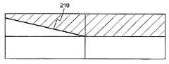
また、車のヘッドライトは、ロービームにした際に上方の光をカットして対向車にまぶしくないようにしつつ路面を照らす必要がある。このロービームにした際に上方の光をカットする境界線は、カットオフライン210と呼ばれ、このカットオフライン210が明瞭でない、すなわち、ロービームにした際にカットオフライン210より上に光が照射されると安全上好ましくない(図14)。そこで、車のヘッドライトは、ロービームにした際にカットオフライン210が明瞭になるように光学系が設計され、ヘッドライト用の光源である発光装置に対しても、カットオフライン210が明瞭になる光学系の設計が可能な輝度特性が求められる。具体的には、発光装置に対しては、例えば、発光面と発光面の外周を囲む光反射性の枠体(被覆部材)との境界が明瞭、すなわち、図13に示すように、その境界を境に外側と内側とで急激に輝度が変化するような特性が求められる。この発光面と発光面の外周を囲む被覆部材との境界を明瞭にするためには、図15に模式的に示すように、発光素子201上に配置する波長変換部材207を大きくして、発光素子201の発光面の外周より波長変換部材207の外周が外側に位置するように、発光素子201上に波長変換部材207を配置して、その発光素子201上に波長変換部材207を囲むように被覆部材を設けることが有効であるとされている。 In addition, the headlights of a car need to illuminate the road surface while cutting off the light above when the low beam is used so as not to dazzle the oncoming vehicle. The boundary line that cuts the upper light when the low beam is set is called the cut-off
しかしながら、発光素子の発光面の外周より蛍光体板の外周が外側に位置するように、発光素子上に蛍光体板(波長変換部材)を配置すると、必然的に発光装置の発光面が大きくなる。発光装置の発光面が大きくなると、ヘッドライトの光学系の構成が大きくなるという課題がある。 However, if the phosphor plate (wavelength conversion member) is arranged on the light emitting element so that the outer periphery of the phosphor plate is located outside the outer periphery of the light emitting surface of the light emitting element, the light emitting surface of the light emitting device inevitably becomes large. .. When the light emitting surface of the light emitting device becomes large, there is a problem that the configuration of the optical system of the headlight becomes large.
そこで、本発明は、ヘッドライトの光源として用いられたときに、簡単でかつ小型の光学系の構成によりカットオフラインを明瞭にできる発光装置を提供することを目的とする。 Therefore, an object of the present invention is to provide a light emitting device capable of clarifying a cut-off line by a simple and compact optical system configuration when used as a light source of a headlight.
以上の目的を達成するために、本発明に係る一実施形態の発光装置は、
基板と、前記基板上に設けられた発光素子と、前記発光素子の発光面である上面に、下面が対向するように設けられた板状の透光性部材と、前記発光素子の側面と透光性部材の側面とを覆う被覆部材と、を備え、
前記発光素子の上面は、互いに対向する第1の辺と第2の辺と互いに対向する第3の辺と第4の辺とを有する矩形形状であり、
前記透光性部材の上面は、互いに対向する第5の辺と第6の辺と互いに対向する第7の辺と第8の辺とを有する矩形形状であり、
前記透光性部材は、上方から平面視したときに、前記第5の辺が前記第1の辺の外側に位置し、前記第6の辺が前記第2の辺の内側に位置するように前記発光素子の上に設けられたことを特徴とする。In order to achieve the above object, the light emitting device of one embodiment according to the present invention is
A substrate, a light emitting element provided on the substrate, a plate-shaped translucent member provided so that a lower surface faces the upper surface of the light emitting surface of the light emitting element, and a side surface and a transparent member of the light emitting element. A covering member that covers the side surface of the optical member,
The upper surface of the light emitting element has a rectangular shape having a first side facing each other, a second side, a third side facing each other, and a fourth side.
The upper surface of the translucent member has a rectangular shape having a fifth side facing each other, a sixth side, a seventh side facing each other, and an eighth side.
The translucent member is such that the fifth side is located outside the first side and the sixth side is located inside the second side when viewed in a plan view from above. It is characterized in that it is provided on the light emitting element.
本発明に係る一実施形態の発光装置は、ヘッドライトの光源として用いられたときに、簡単でかつ小型の光学系の構成によりカットオフラインを明瞭にできる。 When the light emitting device of one embodiment according to the present invention is used as a light source of a headlight, the cut-off line can be clarified by a simple and compact optical system configuration.
本発明者は、ヘッドライトの光源として用いられたときに、簡単でかつ小型の光学系によりカットオフラインを明瞭にできる発光装置を提供するために、鋭意検討した。その結果、発光面が矩形の発光装置において、発光面と発光面の外周を囲む被覆部材との境界のうち、1つの辺の境界において、その境界の外側と内側とで急激に輝度が変化するようにすれば、ヘッドライトの光源として用いられたときに、簡単な光学系の構成によりカットオフラインを明瞭にできることを見いだした。すなわち、矩形の発光面において、1つの辺について輝度が急激に変化する境界とすれば、他の辺の境界において輝度がなだらかに変化してもヘッドライトの光源として用いられたときにカットオフラインを明瞭にできる。本実施形態の発光装置は、以上の知見に基づいてなされたものである。 The present inventor has diligently studied in order to provide a light emitting device capable of clarifying a cut-off line by a simple and compact optical system when used as a light source of a headlight. As a result, in a light emitting device having a rectangular light emitting surface, the brightness changes sharply between the outside and the inside of the boundary of one side of the boundary between the light emitting surface and the covering member surrounding the outer periphery of the light emitting surface. By doing so, it was found that when used as a light source for headlights, the cut-off line can be made clear by a simple optical system configuration. That is, on a rectangular light emitting surface, if the boundary is such that the brightness changes rapidly for one side, the cut-off line is set when the headlight is used as a light source even if the brightness changes gently at the boundary of the other side. Can be clarified. The light emitting device of the present embodiment is made based on the above findings.
具体的には、本実施形態の発光装置では、発光素子の発光面に透光性部材を載置し、透光性部材の周りに被覆部材を設けた構成において、
(1)発光素子の発光面の一つの辺の外側に透光性部材の一つの辺が位置するように発光素子の発光面上に透光性部材を載置して、透光性部材の上記一つの辺と被覆部材の境界で外側と内側とで急激に輝度が変化するようにし、
(2)その一つの辺を除く他の3つの辺のうちのいずれか1つ以上の辺について、発光素子の発光面の一辺の内側に透光性部材の一辺が位置するようにすることにより、内側に配置した分、発光面の面積を小さくしている。
尚、発光素子の発光面の一辺の内側に位置する透光性部材の一辺(発光装置の発光面の一辺)では、その一辺の外側と内側とにおける輝度の変化はなだらかになるが、カットオフラインの明瞭性に対する影響は小さい。
以下、実施形態の発光装置について詳細に説明する。Specifically, in the light emitting device of the present embodiment, a translucent member is placed on the light emitting surface of the light emitting element, and a covering member is provided around the translucent member.
(1) A translucent member is placed on the light emitting surface of the light emitting element so that one side of the translucent member is located outside one side of the light emitting surface of the light emitting element. At the boundary between one side and the covering member, the brightness changes rapidly between the outside and the inside.
(2) For any one or more of the other three sides excluding the one side, one side of the translucent member is located inside one side of the light emitting surface of the light emitting element. , The area of the light emitting surface is reduced by the amount arranged inside.
On one side of the translucent member (one side of the light emitting surface of the light emitting device) located inside one side of the light emitting surface of the light emitting element, the change in brightness between the outside and the inside of the side becomes gentle, but cut-off line. The effect on the clarity of is small.
Hereinafter, the light emitting device of the embodiment will be described in detail.
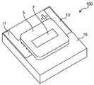
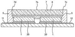
以下、図面を参照しながら本発明に係る実施形態の発光装置について説明する。図1は、本発明に係る実施形態の発光装置の斜視図であり、図2は、実施形態の発光装置の平面図である。また、図3は、図2のA−A線についての断面図であり、図4は、図2のB−B線についての断面図である。 Hereinafter, the light emitting device according to the embodiment of the present invention will be described with reference to the drawings. FIG. 1 is a perspective view of the light emitting device of the embodiment according to the present invention, and FIG. 2 is a plan view of the light emitting device of the embodiment. Further, FIG. 3 is a cross-sectional view taken along the line AA of FIG. 2, and FIG. 4 is a cross-sectional view taken along the line BB of FIG.
実施形態の発光装置100は、
(a)基板10と、
(b)基板10上に設けられた発光素子1と、
(c)発光素子1の発光面である上面に、下面が対向するように設けられた板状の透光性部材7と、
(d)発光素子1の側面と透光性部材7の側面とを覆う被覆部材5と、
を備えている。発光素子1は、図3及び図4に示すように、例えば、導電性接合部材20を介して基板10上にフリップチップ実装されている。尚、図3及び図4における発光素子1は簡略化して示しているが、発光素子1は、例えば、同一面側にp側電極とn側電極とを有してなり、そのp側電極及びn側電極がそれぞれ導電性接合部材20を介して基板10上に設けられた第1電極11又は第2電極12に接続される。透光性部材7は、詳細後述するように、発光素子1の発光面に導光部材40を介して接合される。また、透光性部材7は、発光素子1の光により励起されて、発光素子1が発光する光の波長より長波長の光を発光する蛍光体8を含む。The
(A)
(B) A
(C) A plate-shaped
(D) A covering
Is equipped with. As shown in FIGS. 3 and 4, the
被覆部材5は、例えば、樹脂等からなる母材中に白色顔料を含む反射性部材であり、基板10上において発光素子1の側面、導光部材40の側面及び透光性部材7の側面を被覆している。被覆部材5は、発光素子1及び透光性部材7等の側面を全周にわたって包囲する。また、透光性部材7の上面7s(つまり発光装置100の発光面)と被覆部材5の上面は、実質的に同一面を構成している。以上のように構成された発光装置100は、発光素子1及び透光性部材7から側方に出射される光が被覆部材5によって反射されて上方から出射されるので上方からの光の取り出し効率を高くできる。 The covering
ここで特に、発光装置100において、図2及び図4から理解できるように、透光性部材7を発光素子1上にずらして配置している。このように構成された発光装置100をヘッドライトの光源モジュールとして用いると、簡単でかつ小型の光学系により、配光パターンに明瞭なカットオフラインを有するヘッドライトとできる。 Here, in particular, in the
<発光素子1と透光性部材7の配置>
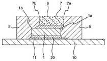
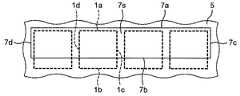
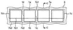
発光素子1の上面は、図2に示すように、互いに対向する第1の辺1aと第2の辺1bと、互いに対向する第3の辺1cと第4の辺1dと、を有する矩形形状である。また、透光性部材7の上面7sは、互いに対向する第5の辺7aと第6の辺7bと、互いに対向する第7の辺7cと第8の辺7dと、を有する矩形形状である。<Arrangement of light emitting
As shown in FIG. 2, the upper surface of the
そして、透光性部材7は、上方から平面視したときに、図2に示すように、第5の辺7aが第1の辺1aの外側に位置し、第6の辺7bが第2の辺1bの内側に位置するように発光素子1の上に設けられる。ここで、実施形態の発光装置は、図2等に示すように複数の発光素子1を含んでおり、透光性部材7は、図2に示すように、透光性部材7の第5の辺7aが2つの発光素子1の第1の辺1aの外側に位置し、第6の辺7bが2つの発光素子1の第2の辺1bの内側に位置するように、2つの発光素子1の上に設けられる。
ここで、本実施形態の発光装置100において、それぞれ第1の辺1a〜第4の辺1dを有する複数の発光素子1を含む場合には、複数の発光素子1は第1の辺1aがそれぞれ同一直線(第1直線)上に位置することが好ましい。さらに、複数の発光素子1は、第1の辺1aがそれぞれ第1直線上に位置し、第2の辺1bが第1直線に平行な第2直線上にそれぞれ位置するように基板10上に配列されていることがより好ましい。
さらに、透光性部材7の上面7sは、実質的に平坦で、透光性部材7の下面に略平行な面であることが好ましい。また、透光性部材7の上面7sに連なる側面のうち、第5の辺7aを介して上面7sに連なる側面は、下面に連なり、かつ、上面7sに略垂直な面であることが好ましい。When the
Here, in the
Further, it is preferable that the
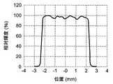
以上のように構成された実施形態の発光装置100は、上方から平面視したときに、透光性部材7の第5の辺7aが発光素子1の第1の辺1aの外側に位置するように、透光性部材7が設けられている。このため、透光性部材7の第5の辺7aに対応する発光面と被覆部材5との境界を境に外側と内側の輝度の変化を急峻にできる(図5に示すグラフにおける左側の相対輝度の立ち上がり部)。これにより、発光装置100をヘッドライトの光源として用いたときに、簡単な構成の光学系によりカットオフラインが明瞭なヘッドライトとできる。 In the
また、実施形態の発光装置100は、上方から平面視したときに、透光性部材7の第6の辺7bが発光素子1の第2の辺1bの内側に位置するように、透光性部材7が発光素子1の上に設けられているので、透光性部材7の上面7sの幅を狭く、言い換えれば、発光装置100の発光面の幅を狭くできる。つまり、発光面の面積を小さくできる。これにより、発光装置100をヘッドライトの光源として用いたときに、光学系を小型にできる。尚、透光性部材7の第6の辺7bが発光素子1の第2の辺1bの内側に位置するように、透光性部材7が発光素子1の上に設けられていると、透光性部材7の第6の辺7bに対応する発光面と被覆部材5との境界の外側と内側の輝度の変化がなだらかになる(図5に示すグラフにおける右側の相対輝度の立ち上がり部)。しかしながら、実施形態の発光装置100は、上方から平面視したときに、透光性部材7の第5の辺7aが発光素子1の第1の辺1aの外側に位置するように、透光性部材7が設けられているので、透光性部材7の第6の辺7bが発光素子1の第2の辺1bの内側に位置することによるカットオフラインの明瞭性に対する影響は少ない。ここで、図5に示す相対輝度のグラフは、図2に示すB−B線についての断面における相対輝度を示している。 Further, the
以上説明したように、実施形態1の発光装置100によれば、発光装置100をヘッドライトの光源として用いることにより、簡単でかつ小型の光学系によりカットオフラインが明瞭なヘッドライトを構成することが可能になる。 As described above, according to the
以上の実施形態の発光装置において、透光性部材7の第7の辺7c及び第8の辺7dがそれぞれ発光素子1の第3の辺1c及び第4の辺1dの外側に位置するように透光性部材7が設けられている。これにより、第7の辺7c及び第8の辺7dを境にして外側と内側との間の輝度の変化を急峻にでき、発光装置100をヘッドライトの光源として用いたときに、より簡単な構成の光学系によりカットオフラインが明瞭なヘッドライトとできる。 In the light emitting device of the above embodiment, the
実施形態の発光装置において、透光性部材7を、第7の辺7c及び第8の辺7dがそれぞれ第3の辺1c及び第4の辺1dの内側に位置するように発光素子1の上に設けてもよい。このようにすると、発光装置100の発光面の面積をより小さくできるので、発光装置100をヘッドライトの光源として用いたときに、光学系をより小型にできる。 In the light emitting device of the embodiment, the
実施形態の発光装置において、透光性部材7は、第7の辺7cが第3の辺1cの内側に位置し、第8の辺7dが第4の辺1dの外側に位置するように発光素子の上に設けられていてもよい。 In the light emitting device of the embodiment, the
以上の実施形態の発光装置では、1つの透光性部材7が複数の発光素子1を覆うように構成した。
しかしながら、実施形態の発光装置はこれに限定されるものではなく、1つの透光性部材7が1つの発光素子1を覆う構成としてもよい。また、後述の変形例で示すように、それぞれ1又は2以上の発光素子1を覆う複数の透光性部材7を設けるようにしてもよい。In the light emitting device of the above embodiment, one
However, the light emitting device of the embodiment is not limited to this, and one
以上の実施形態の発光装置では、透光性部材7を、上方から平面視したときに、第5の辺7aが第1の辺1aの外側に位置し、第6の辺7bが第2の辺1bの内側に位置するように発光素子1の上に設けた。
しかしながら、実施形態の発光装置はこれに限定されるものではなく、透光性部材7は、上方から平面視したときに、第5の辺7aが第1の辺1aに重なるようにし、第6の辺7bが第2の辺1bの内側に位置するように発光素子1の上に設けられていてもよい。In the light emitting device of the above embodiment, when the
However, the light emitting device of the embodiment is not limited to this, and the
以上の実施形態の発光装置は、蛍光体8を含む透光性部材7により構成した。
しかしながら、実施形態の発光装置はこれに限定されるものではなく、蛍光体を含まない透光性部材7により構成するようにしてもよい。The light emitting device of the above embodiment is composed of a
However, the light emitting device of the embodiment is not limited to this, and may be configured by a
変形例1
図6は、本発明に係る変形例1の発光装置の平面図である。
この変形例1の発光装置は、4つの発光素子1を用いて構成した点が図2等に示す発光装置とは異なっている他は実施形態の発光装置と同様である。
以上のように構成された変形例1の発光装置は、実施形態の発光装置と同様の作用効果を有し、図2等に示す発光装置に比較してより輝度を高くできる。
FIG. 6 is a plan view of the light emitting device of the first modification according to the present invention.
The light emitting device of the first modification is the same as the light emitting device of the embodiment except that it is different from the light emitting device shown in FIG. 2 and the like in that it is configured by using four
The light emitting device of the modified example 1 configured as described above has the same function and effect as the light emitting device of the embodiment, and can have higher brightness than the light emitting device shown in FIG. 2 and the like.
変形例2
図7は、本発明に係る変形例2の発光装置の平面図である。また、図8は、変形例2の発光装置の断面図であり、図7におけるC−C線についての断面を示している。
この変形例2の発光装置は、透光性部材7の形状が変形例1の発光装置とは異なっている他は、変形例1の発光装置と同様に構成されている。変形例2の発光装置において、透光性部材7は、変形例2の透光性部材7の上面7s(以下、第1上面という。)の外側に第1上面より下に位置する第2上面を含み、その第2上面が被覆部材5により覆われている。以下、実施形態及び変形例1と相違する点を具体的に説明する。
FIG. 7 is a plan view of the light emitting device of the second modification according to the present invention. Further, FIG. 8 is a cross-sectional view of the light emitting device of the modified example 2, and shows a cross section of the line CC in FIG.
The light emitting device of the modified example 2 is configured in the same manner as the light emitting device of the modified example 1, except that the shape of the
変形例2の発光装置において、透光性部材7は、発光素子1に接合される下面と該下面に対向する上面とを有している。透光性部材7の下面は実質的に平坦な一つの下面で構成されるのに対して、その上面は、第1上面7s1と第2上面7s2との少なくとも2つの上面を有する。第1上面7s1と第2上面7s2とはその間に段差を有する。具体的には、第2上面7s2の下の透光性部材7の厚みが第1上面7s1の下の透光性部材7の厚みより薄くなっている。 In the light emitting device of the second modification, the
変形例2の発光装置において、透光性部材7の第1上面7s1は、第5の辺7aと、第5の辺7aに対向する第6の内側辺7b1とを有する。透光性部材7の第2上面7s2は、第6の内側辺7b1の外側に位置する第6の外側辺7b2を有している。 In the light emitting device of the second modification, the first upper surface 7s1 of the
そして、変形例2の発光装置において、透光性部材7は、上方から平面視したときに、図7及び図8に示すように、(a)第5の辺7aが発光素子1の第1の辺1aの外側に位置し、(b)第6の内側辺7b1が発光素子1の第2の辺1bの内側に位置し、(c)第6の外側辺7b2が発光素子1の第2の辺1bの外側に位置するように、発光素子1の上に設けられる。
なおこの際、透光性部材7の第1上面7s1は、実質的に平坦で、下面に略平行な面であることが好ましく、透光性部材7の第1上面7s1に連なる側面のうち、少なくとも第5の辺7aを介して第1上面7s1に連なる側面は、下面に連なり、かつ、第1上面7s1に略垂直な面であることが好ましい。また、第2上面7s2は、下面に対して略平行な面であってもよいし、下面に対して傾斜する傾斜面であってもよい。Then, in the light emitting device of the second modification, when the
At this time, it is preferable that the first upper surface 7s1 of the
変形例2の発光装置において、被覆部材5は、第1上面7s1を露出させ、第2上面7s2を覆うように設けられる。これにより、透光性部材7の第1上面7s1が発光装置の発光面となる。 In the light emitting device of the second modification, the covering
以上のように構成された変形例2の発光装置は、上方から平面視したときに、透光性部材7の第5の辺7aが発光素子1の第1の辺1aの外側に位置するように、透光性部材7が設けられているので、透光性部材7の第5の辺7aに対応する発光面と被覆部材5との境界の外側と内側の輝度の変化を急峻にできる。これにより、変形例2の発光装置をヘッドライトの光源として用いたときに、簡単な構成の光学系によりカットオフラインが明瞭なヘッドライトとできる。 In the light emitting device of the modified example 2 configured as described above, the
また、変形例2の発光装置は、上方から平面視したときに、透光性部材7の第6の内側辺7b1が発光素子1の第2の辺1bの内側に位置するように、透光性部材7が発光素子1の上に設けられているので、透光性部材7の第1上面7s1の幅を狭く、言い換えれば、発光装置の発光面の幅を狭くでき、発光面の面積を小さくできる。これにより、発光装置100をヘッドライトの光源として用いたときに、光学系を小型にできる。 Further, the light emitting device of the modified example 2 transmits light so that the sixth inner side 7b1 of the
また、変形例2の発光装置において、透光性部材7が蛍光体を含んでいる場合には、つまり、発光装置の所望の発光色が、蛍光体により波長変換された光を含むことにより得られる場合には、透光性部材7の下面が発光素子1の発光面の全体を覆っているので、発光素子から出射された光が透光性部材7を介さずに、外部に漏れ伝わることを防止することができる。 Further, in the light emitting device of the second modification, when the
変形例3
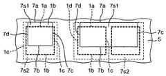
図9は、本発明に係る変形例3の発光装置の平面図である。
この変形例3の発光装置は、3つの発光素子1と2つの透光性部材7を備えている点で実施形態の発光装置とは異なっている。
FIG. 9 is a plan view of the light emitting device of the third modification according to the present invention.
The light emitting device of the third modification is different from the light emitting device of the embodiment in that it includes three light emitting
変形例3の発光装置において、2つの発光素子1の上に1つの透光性部材7が設けられ、1つの発光素子1の上に透光性部材7が設けられている。具体的には、2つのうちの一方の透光性部材7は、上方から平面視したときに、図9に示すように、第5の辺7aが2つの発光素子1の第1の辺1aの外側に位置し、第6の辺7bが2つの発光素子1の第2の辺1bの内側に位置するように2つの発光素子1に跨がって設けられている。
また、2つのうちの他方の透光性部材7は、上方から平面視したときに、図9に示すように、第5の辺7aが1つの発光素子1の第1の辺1aの外側に位置し、第6の辺7bが1つの発光素子1の第2の辺1bの内側に位置するように発光素子1の上に設けられている。
このように、発光装置が複数の発光素子1を有する場合、所望の配光パターンに適した光源として、透光性部材7と、発光素子1の数、間隔、配置密度等を組み合わせることができる。In the light emitting device of the third modification, one
Further, as shown in FIG. 9, the other
As described above, when the light emitting device has a plurality of
変形例3の発光装置において、透光性部材7の第7の辺7c及び第8の辺7dはそれぞれ発光素子1の第3の辺1c及び第4の辺1dの外側に位置するように2つの透光性部材7が設けられている。 In the light emitting device of the third modification, the
以上のように構成された変形例3の発光装置は、発光装置100をヘッドライトの光源として用いたときに、より簡単な構成の光学系により配光パターンのカットオフラインが明瞭なヘッドライトとできる。
また、変形例3の発光装置は、発光面の面積をより小さくできるので、変形例3の発光装置をヘッドライトの光源として用いたときに、光学系をより小型にできる。When the
Further, since the light emitting device of the modified example 3 can have a smaller area of the light emitting surface, the optical system can be made smaller when the light emitting device of the modified example 3 is used as a light source of a headlight.
変形例4
図10は、本発明に係る変形例4の発光装置の平面図である。
この変形例4の発光装置は、変形例3の発光装置において、透光性部材7の第7の辺7c及び第8の辺7dをそれぞれ発光素子1の第3の辺1c及び第4の辺1dの内側に位置するように2つの透光性部材7を設けた以外は変形例3の発光装置と同様に構成されている。
以上のように構成された変形例4の発光装置は、変形例3の発光装置に比較して発光面の面積をより小さくできるので、変形例4の発光装置をヘッドライトの光源として用いたときに、光学系をより小型にできる。
FIG. 10 is a plan view of the light emitting device of the modified example 4 according to the present invention.
In the light emitting device of the modified example 4, the light emitting device of the modified example 3 has the
Since the light emitting device of the modified example 4 configured as described above can have a smaller area of the light emitting surface than the light emitting device of the modified example 3, when the light emitting device of the modified example 4 is used as a light source of the headlight. In addition, the optical system can be made smaller.
変形例5
図11は、本発明に係る変形例5の発光装置の平面図である。
この変形例5の発光装置は、2つの透光性部材7の形状が変形例4の発光装置と異なっている他は、変形例4の発光装置と同様に構成されている。
FIG. 11 is a plan view of the light emitting device of the modified example 5 according to the present invention.
The light emitting device of the modified example 5 is configured in the same manner as the light emitting device of the modified example 4, except that the shapes of the two
具体的には、変形例5の発光装置において、透光性部材7は、変形例4の透光性部材7の上面(第1上面7s1)の外側に第1上面より下に位置する第2上面7s2を含み、その第2上面7s2が被覆部材5により覆われている。また、変形例5の発光装置の透光性部材7において第2上面7s2は、上方から平面視したときに、第5の辺7aを除く3辺を囲むように設けられている。また、変形例5の発光装置において、透光性部材7はそれぞれ発光素子1に接合される実質的に平坦な下面を有している。 Specifically, in the light emitting device of the modified example 5, the
変形例5の発光装置において、透光性部材7の第1上面7s1は、上方からみた平面視において、発光素子1に対して変形例4の発光装置における透光性部材7の上面7sと同様の位置関係になるように配置される。また、透光性部材7はそれぞれ下面が発光素子1の外周の外側に位置するように発光素子1上に設けられる。 In the light emitting device of the modified example 5, the first upper surface 7s1 of the
以上のように構成された変形例5の発光装置は、ヘッドライトの光源として用いたときに、より簡単な構成の光学系によりカットオフラインが明瞭なヘッドライトとできる。
また、変形例5の発光装置は、発光面の面積をより小さくできるので、より高緯度な発光装置とすることが可能になる。また、ヘッドライトの光源として用いたときに、光学系をより小型にできる。When the light emitting device of the modified example 5 configured as described above is used as a light source of a headlight, a headlight having a clear cut-off line can be obtained by an optical system having a simpler configuration.
Further, since the light emitting device of the modified example 5 can have a smaller area of the light emitting surface, it is possible to make the light emitting device at a higher latitude. Further, when used as a light source for a headlight, the optical system can be made smaller.
以上のように構成された変形例5の発光装置は、変形例4の発光装置と同様の作用効果を有し、さらに透光性部材7が蛍光体を含んでいる場合には、透光性部材7が発光素子1の発光面の全体を覆っているので、発光素子1が発光する光を効率良く蛍光体8に照射できる。 The light emitting device of the modified example 5 configured as described above has the same function and effect as the light emitting device of the modified example 4, and further, when the
変形例6
図12は、本発明に係る変形例6の発光装置の平面図である。
この変形例6の発光装置において、透光性部材7は、第1上面7s1の外側に第1上面7s1より下に位置する第2上面7s2を含み、その第2上面7s2が被覆部材5により覆われている。そして、透光性部材7は、上方から平面視したときに、図12に示すように、第5の辺7aが発光素子1の第1の辺1aの外側に位置し、第6の内側辺7b1及び第6の外側辺7b2がいずれも発光素子1の第2の辺1bの内側に位置するように発光素子1の上に設けられている。尚、変形例6の発光装置において、透光性部材7の第7の辺7c及び第8の辺7dはいずれも発光素子1の第3の辺1c及び第4の辺1dの外側に位置する。Modification 6
FIG. 12 is a plan view of the light emitting device of the modified example 6 according to the present invention.
In the light emitting device of the modification 6, the
以上のように構成された変形例6の発光装置は、ヘッドライトの光源として用いたときに、より簡単な構成の光学系によりカットオフラインが明瞭なヘッドライトとできる。
また、変形例6の発光装置は、発光面の面積をより小さくできるので、ヘッドライトの光源として用いたときに、光学系をより小型にできる。When the light emitting device of the modified example 6 configured as described above is used as a light source of a headlight, the headlight having a clear cut-off line can be obtained by an optical system having a simpler configuration.
Further, since the light emitting device of the modified example 6 can have a smaller area of the light emitting surface, the optical system can be made smaller when used as a light source of a headlight.
以下に、本実施形態及び変形例における発光装置の各部材及び構造について説明する。 Hereinafter, each member and structure of the light emitting device in the present embodiment and the modified example will be described.
(基板10)
基板10は、発光素子を配置させるための部材であり、発光素子の電極と外部電極を電気的に接続するための配線を有する。基板10の主な材料としては、絶縁性材料であって、発光素子からの光及び外光が透過しにくい材料が好ましい。例えば、アルミナや窒化アルミニウム等のセラミックス、フェノール樹脂、エポキシ樹脂、ポリイミド樹脂、BTレジン、ポリフタルアミド等の樹脂を挙げることができる。なお、樹脂を用いる場合には、必要に応じて、ガラス繊維、酸化ケイ素、酸化チタン、アルミナ等の無機フィラーを樹脂に混合してもよい。これにより、機械的強度の向上や熱膨張率の低減、光反射率の向上を図ることができる。また、基板10は、金属部材の表面に絶縁性材料を形成したものでもよい。配線は、上記絶縁性材料の上に、所定のパターンで形成される。配線の材料として、金、銀、銅およびアルミニウムから選択された少なくとも一種とすることができる。配線は、めっき、蒸着、スパッタ等によって形成することができる。(Board 10)
The
(発光素子1)
発光素子1としては、発光ダイオードを用いるのが好ましい。発光素子は、任意の波長のものを選択することができる。例えば、青色、緑色の発光素子としては、ZnSeや窒化物系半導体(InXAlYGa1−X−YN、0≦X、0≦Y、X+Y≦1)、GaPを用いたものを用いることができる。また、赤色の発光素子としては、GaAlAs、AlInGaPなどを用いることができる。さらに、これ以外の材料からなる半導体発光素子を用いることもできる。用いる発光素子の組成や発光色、大きさや、個数などは目的に応じて適宜選択することができる。蛍光体を有する発光装置とする場合には、その蛍光体を効率良く励起できる短波長が発光可能な窒化物半導体(InXAlYGa1−X−YN、0≦X、0≦Y、X+Y≦1)が好適に挙げられる。半導体層の材料やその混晶度によって発光波長を種々選択することができる。(Light emitting element 1)
It is preferable to use a light emitting diode as the
実施形態の発光素子は、同一面側に正負の電極を有するものであり、正負の電極が導電性接合部材を介して基板上にフリップチップ実装されている。発光素子は、電極の形成された下面と対向する上面を主な光出射面としている。このような発光素子は、バンプや導電ペーストなどの導電性接合部材を用いて基板上に接続されるため、金属ワイヤなどで接続される発光素子と比較して、電極と基板との接触面積を大きくでき、接続抵抗を低くできる。 The light emitting element of the embodiment has positive and negative electrodes on the same surface side, and the positive and negative electrodes are flip-chip mounted on the substrate via a conductive bonding member. The light emitting element has an upper surface facing the lower surface on which the electrodes are formed as a main light emitting surface. Since such a light emitting element is connected on the substrate by using a conductive bonding member such as a bump or a conductive paste, the contact area between the electrode and the substrate is larger than that of the light emitting element connected by a metal wire or the like. It can be made larger and the connection resistance can be lowered.
発光素子は、例えば、透光性の成長用のサファイア基板上に窒化物半導体層を積層させて形成された発光素子であり、サファイア基板が発光素子1の上面側となり、主な光出射面となる。なお、成長用基板は除去してもよく、例えば、研磨、LLO(Laser Lift Off)等で除去することができる。 The light emitting element is, for example, a light emitting element formed by laminating a nitride semiconductor layer on a sapphire substrate for translucent growth, and the sapphire substrate is on the upper surface side of the
(透光性部材7)
透光性部材7は、発光素子1から出射される光を透過して外部に放出することが可能な材料である。透光性部材7は、光拡散材や、入射された光の少なくとも一部を波長変換可能な蛍光体を含有させてもよい。透光性部材7は、例えば、樹脂、ガラス、無機物等により形成することができる。蛍光体を含有する透光性部材は、例えば、蛍光体の焼結体や、樹脂、ガラス、セラミック又は他の無機物に蛍光体を含有させたもの等が挙げられる。また、樹脂、ガラス、セラミック等の成形体の表面に蛍光体を含有する樹脂層を形成したものでもよい。透光性部材7の厚みは、例えば、50〜300μm程度である。
透光性部材7と発光素子との接合は、例えば後述する導光部材を介して接合することができる。また、透光性部材と発光素子との接合には、圧着、焼結、表面活性化接合、原子拡散接合、水酸基接合による直接接合法を用いてもよい。(Translucent member 7)
The
The
(蛍光体)
透光性部材7に含有させることができる蛍光体としては、発光素子からの発光で励起可能なものが使用される。例えば、青色発光素子又は紫外線発光素子で励起可能な蛍光体としては、セリウムで賦活されたイットリウム・アルミニウム・ガーネット系蛍光体(Ce:YAG);セリウムで賦活されたルテチウム・アルミニウム・ガーネット系蛍光体(Ce:LAG);ユウロピウムおよび/又はクロムで賦活された窒素含有アルミノ珪酸カルシウム系蛍光体(CaO−Al2O3−SiO2);ユウロピウムで賦活されたシリケート系蛍光体((Sr,Ba)2SiO4);βサイアロン蛍光体、CASN系蛍光体、SCASN系蛍光体等の窒化物系蛍光体;KSF系蛍光体(K2SiF6:Mn);硫化物系蛍光体、量子ドット蛍光体などが挙げられる。これらの蛍光体と、青色発光素子又は紫外線発光素子と組み合わせることにより、様々な色の発光装置(例えば白色系の発光装置)を製造することができる。(Fluorescent material)
As the phosphor that can be contained in the
(被覆部材5)
被覆部材5は、発光素子1および透光性部材7の側面を被覆する。被覆部材5は、例えば、光反射率の高い光反射性材料から形成することができる。具体的には、被覆部材5は、発光素子からの光に対する反射率が60%以上、より好ましくは80%又は90%以上である光反射性材料を用いることができる。光反射性材料は、例えば、光反射性物質を含む樹脂からなる。
被覆部材5を構成する母体の樹脂としては、シリコーン樹脂、変性シリコーン樹脂、エポキシ樹脂、変性エポキシ樹脂、アクリル樹脂、また、これらの樹脂を少なくとも一種以上含むハイブリッド樹脂等の樹脂を用いることができ、その樹脂からなる母材に反射性物質を含有させることで形成することができる。光反射性物質としては、Ti、Zr、Nb、Al、Siのいずれかを含む酸化物、または、AlN、MgFなどを用いることができる。好ましくは二酸化チタン(TiO2)を用いる。また、好ましくは、光反射性物質として、母材の樹脂の屈折率と異なる粒子を母材の樹脂中に分散させる。光反射性物質の含有濃度、密度により光の反射量、透過量が異なるため、発光装置の形状、大きさに応じて、適宜濃度、密度を調整することができる。(Coating member 5)
The covering
As the base resin constituting the
(導光部材40)
発光装置は、発光素子1の側面を被覆する導光部材40を備えていてもよい。発光素子1の上面の一部が透光性部材7から露出する場合、導光部材40は、透光性部材7から露出する発光素子の上面を被覆することが好ましい。さらに、導光部材40は、発光素子1から露出する透光性部材7の下面を被覆することが好ましい。なお、導光部材40は発光素子と透光性部材7との間にも介在し、両者を接合するための接着部材としても用いることができる。このような導光部材40を備えることにより、発光素子1の上面及び側面からの出射光が導光部材40の外面で反射し、反射光を透光性部材7へと導光させることができる。(Light guide member 40)
The light emitting device may include a
導光部材40は、取り扱いおよび加工が容易であるという観点から、樹脂材料を用いることが好ましい。樹脂材料としては、シリコーン樹脂、変性シリコーン樹脂、エポキシ樹脂、変性エポキシ樹脂、アクリル樹脂、フッ素樹脂の1種以上を含む樹脂またはハイブリッド樹脂等からなる樹脂材料を用いることができる。導光部材40は、導光部材40を形成するための樹脂材料の粘性、樹脂材料と発光素子1との濡れ性を利用して形成することができる。 It is preferable to use a resin material for the
発光装置は、任意に、保護素子等の別の素子、電子部品等を有していてもよい。これらの素子及び電子部品は、被覆部材5内に埋設されていることが好ましい。 The light emitting device may optionally have another element such as a protective element, an electronic component, or the like. It is preferable that these elements and electronic components are embedded in the covering
1 発光素子
1a 第1の辺1a
1b 第2の辺1b
1c 第3の辺1c
1d 第4の辺1d
5 被覆部材
7 透光性部材
7a 第5の辺7a
7b 第6の辺7b
7b1 第6の内側辺
7b2 第6の外側辺
7c 第7の辺7c
7d 第8の辺7d
7s 上面
7s1 第1上面
7s2 第2上面
8 蛍光体
10 基板
20 導電性接合部材
40 導光部材
100 発光装置1
5 Covering
7b
7b1 6th inner side 7b2 6th
7s upper surface 7s1 first upper surface 7s2 second
Claims (9)
Translated fromJapanese前記基板上に設けられた発光素子と、
前記発光素子の発光面である上面に、下面が対向するように設けられた板状の透光性部材と、
前記発光素子の側面と透光性部材の側面とを覆う被覆部材と、
を備え、
前記発光素子の上面は、互いに対向する第1の辺と第2の辺と互いに対向する第3の辺と第4の辺とを有する矩形形状であり、
前記透光性部材は、
前記被覆部材から露出し、互いに対向する第5の辺と第6の内側辺と互いに対向する第7の辺と第8の辺とを有する矩形形状の第1上面と、
前記第1上面の外側に位置しかつ前記被覆部材に覆われた第2上面と、を有し、
前記透光性部材は、上方から平面視したときに、前記第5の辺が前記第1の辺の外側に位置し、前記第6の内側辺が前記第2の辺の内側に位置し、かつ前記第2上面における第6の内側辺に対向する第6の外側辺が前記第2の辺の外側に位置するように前記発光素子の上に設けられたことを特徴とする発光装置。With the board
The light emitting element provided on the substrate and
A plate-shaped translucent member provided so that the lower surface faces the upper surface, which is the light emitting surface of the light emitting element.
A covering member that covers the side surface of the light emitting element and the side surface of the translucent member,
With
The upper surface of the light emitting element has a rectangular shape having a first side facing each other, a second side, a third side facing each other, and a fourth side.
The translucent member is
A rectangular first upper surface exposed from the covering member and having a fifth side facing each other, a sixth inner side, and a seventh side and an eighth side facing each other.
It has a second upper surface located outside the first upper surface and covered with the covering member.
When the translucent member is viewed in a plan view from above, the fifth side is located outside the first side, and the sixth inner side is located inside the second side. Further, the light emitting device is provided on the light emitting element so that the sixth outer side facing the sixth inner side on the second upper surface is located outside the second side.
前記基板上に設けられた発光素子と、
前記発光素子の発光面である上面に、下面が対向するように設けられた板状の透光性部材と、
前記発光素子の側面と透光性部材の側面とを覆う被覆部材と、
を備え、
前記発光素子の上面は、互いに対向する第1の辺と第2の辺と互いに対向する第3の辺と第4の辺とを有する矩形形状であり、
前記透光性部材は、
前記被覆部材から露出し、互いに対向する第5の辺と第6の内側辺と互いに対向する第7の辺と第8の辺とを有する矩形形状の第1上面と、
前記第1上面の外側に位置しかつ前記被覆部材に覆われた第2上面と、を有し、
前記透光性部材は、上方から平面視したときに、前記第5の辺が前記第1の辺に重なり、前記第6の内側辺が前記第2の辺の内側に位置し、かつ前記第2上面における第6の内側辺に対向する第6の外側辺が前記第2の辺の外側に位置するように前記発光素子の上に設けられたことを特徴とする発光装置。With the board
The light emitting element provided on the substrate and
A plate-shaped translucent member provided so that the lower surface faces the upper surface, which is the light emitting surface of the light emitting element.
A covering member that covers the side surface of the light emitting element and the side surface of the translucent member,
With
The upper surface of the light emitting element has a rectangular shape having a first side facing each other, a second side, a third side facing each other, and a fourth side.
The translucent member is
A rectangular first upper surface exposed from the covering member and having a fifth side facing each other, a sixth inner side, and a seventh side and an eighth side facing each other.
It has a second upper surface located outside the first upper surface and covered with the covering member.
When the translucent member is viewed in a plan view from above, the fifth side overlaps the first side, the sixth inner side is located inside the second side, and the first side is 2. A light emitting device characterized in that a sixth outer side facing the sixth inner side on the upper surface is provided on the light emitting element so as to be located outside the second side.
Priority Applications (10)
| Application Number | Priority Date | Filing Date | Title |
|---|---|---|---|
| JP2017191476AJP6806023B2 (en) | 2017-09-29 | 2017-09-29 | Light emitting device |
| US16/143,363US10770630B2 (en) | 2017-09-29 | 2018-09-26 | Light-emitting device |
| CN202311385541.6ACN117673232A (en) | 2017-09-29 | 2018-09-27 | Light emitting device |
| CN201811130142.4ACN109616567B (en) | 2017-09-29 | 2018-09-27 | Lighting device |
| DE102018123851.7ADE102018123851B4 (en) | 2017-09-29 | 2018-09-27 | Light emitting device |
| KR1020180115946AKR102607320B1 (en) | 2017-09-29 | 2018-09-28 | Light-emitting device |
| US16/939,937US11195979B2 (en) | 2017-09-29 | 2020-07-27 | Light-emitting device |
| US17/499,362US11870017B2 (en) | 2017-09-29 | 2021-10-12 | Light-emitting device |
| US18/522,392US12183861B2 (en) | 2017-09-29 | 2023-11-29 | Light-emitting device |
| US18/963,274US20250098377A1 (en) | 2017-09-29 | 2024-11-27 | Light-emitting device |
Applications Claiming Priority (1)
| Application Number | Priority Date | Filing Date | Title |
|---|---|---|---|
| JP2017191476AJP6806023B2 (en) | 2017-09-29 | 2017-09-29 | Light emitting device |
Related Child Applications (1)
| Application Number | Title | Priority Date | Filing Date |
|---|---|---|---|
| JP2020200935ADivisionJP7044990B2 (en) | 2020-12-03 | 2020-12-03 | Light emitting device |
Publications (2)
| Publication Number | Publication Date |
|---|---|
| JP2019067905A JP2019067905A (en) | 2019-04-25 |
| JP6806023B2true JP6806023B2 (en) | 2020-12-23 |
Family
ID=65728095
Family Applications (1)
| Application Number | Title | Priority Date | Filing Date |
|---|---|---|---|
| JP2017191476AActiveJP6806023B2 (en) | 2017-09-29 | 2017-09-29 | Light emitting device |
Country Status (5)
| Country | Link |
|---|---|
| US (5) | US10770630B2 (en) |
| JP (1) | JP6806023B2 (en) |
| KR (1) | KR102607320B1 (en) |
| CN (2) | CN117673232A (en) |
| DE (1) | DE102018123851B4 (en) |
Families Citing this family (9)
| Publication number | Priority date | Publication date | Assignee | Title |
|---|---|---|---|---|
| JP6484982B2 (en)* | 2014-09-30 | 2019-03-20 | 日亜化学工業株式会社 | Method for manufacturing light emitting device |
| US20200203567A1 (en)* | 2018-12-21 | 2020-06-25 | Lumileds Holding B.V. | Led package with increased contrast ratio |
| JP7271302B2 (en)* | 2019-05-16 | 2023-05-11 | スタンレー電気株式会社 | semiconductor light emitting device |
| JP7267836B2 (en)* | 2019-05-16 | 2023-05-02 | スタンレー電気株式会社 | light emitting device |
| JP7269792B2 (en)* | 2019-05-16 | 2023-05-09 | スタンレー電気株式会社 | light emitting device |
| JP7108196B2 (en) | 2019-12-26 | 2022-07-28 | 日亜化学工業株式会社 | Light-emitting device, method for manufacturing wavelength conversion member, and method for manufacturing light-emitting device |
| EP4310912A1 (en) | 2022-07-21 | 2024-01-24 | Nichia Corporation | Light-emitting device |
| JP7575704B2 (en)* | 2022-07-21 | 2024-10-30 | 日亜化学工業株式会社 | Light-emitting device |
| JP2024085446A (en)* | 2022-12-15 | 2024-06-27 | 日亜化学工業株式会社 | Light-emitting device |
Family Cites Families (25)
| Publication number | Priority date | Publication date | Assignee | Title |
|---|---|---|---|---|
| US20050211991A1 (en)* | 2004-03-26 | 2005-09-29 | Kyocera Corporation | Light-emitting apparatus and illuminating apparatus |
| WO2007034367A1 (en) | 2005-09-19 | 2007-03-29 | Koninklijke Philips Electronics N.V. | Variable color light emitting device and method for controlling the same |
| DE102006005299A1 (en) | 2006-02-06 | 2007-08-09 | Osram Opto Semiconductors Gmbh | Housing for a light-emitting diode component and light-emitting diode component |
| JP5326705B2 (en) | 2009-03-17 | 2013-10-30 | 日亜化学工業株式会社 | Light emitting device |
| WO2010143114A1 (en) | 2009-06-11 | 2010-12-16 | Koninklijke Philips Electronics N.V. | Led illumination device |
| JP2012169189A (en)* | 2011-02-15 | 2012-09-06 | Koito Mfg Co Ltd | Light-emitting module and vehicular lamp |
| JP2013089769A (en) | 2011-10-18 | 2013-05-13 | Koito Mfg Co Ltd | Light emitting module |
| JP2013110199A (en) | 2011-11-18 | 2013-06-06 | Citizen Electronics Co Ltd | Led light-emitting device |
| GB2498977B (en) | 2012-02-01 | 2015-10-07 | Bae Systems Plc | Drilling apparatus and method |
| WO2014076610A1 (en) | 2012-11-16 | 2014-05-22 | Koninklijke Philips N.V. | Led-based lighting device and manufacture thereof |
| TW201434183A (en)* | 2013-02-20 | 2014-09-01 | Lextar Electronics Corp | Light module |
| JP6172455B2 (en) | 2013-10-07 | 2017-08-02 | 豊田合成株式会社 | Light emitting device |
| JP6303805B2 (en) | 2014-05-21 | 2018-04-04 | 日亜化学工業株式会社 | Light emitting device and manufacturing method thereof |
| JP6661964B2 (en) | 2014-10-28 | 2020-03-11 | 日亜化学工業株式会社 | Light emitting device |
| US9601668B2 (en) | 2014-10-28 | 2017-03-21 | Nichia Corporation | Light emitting device |
| TWI722925B (en)* | 2014-12-08 | 2021-03-21 | 荷蘭商露明控股公司 | Wavelength converted semiconductor light emitting device |
| KR102346798B1 (en)* | 2015-02-13 | 2022-01-05 | 삼성전자주식회사 | Semiconductor light emitting device |
| TW201631808A (en) | 2015-02-25 | 2016-09-01 | 隆達電子股份有限公司 | Light-emitting diode chip package |
| JP6065135B2 (en)* | 2015-04-02 | 2017-01-25 | 日亜化学工業株式会社 | Light emitting device |
| JP2016028461A (en) | 2015-11-27 | 2016-02-25 | シチズン電子株式会社 | LED light-emitting device |
| JP6332294B2 (en)* | 2015-11-30 | 2018-05-30 | 日亜化学工業株式会社 | Light emitting device |
| EP3174110B1 (en) | 2015-11-30 | 2020-12-23 | Nichia Corporation | Light emitting device |
| JP6399017B2 (en) | 2016-02-29 | 2018-10-03 | 日亜化学工業株式会社 | Light emitting device |
| JP6196703B1 (en) | 2016-04-14 | 2017-09-13 | レノボ・シンガポール・プライベート・リミテッド | Apparatus, electronic device and method for supplying electric power to electronic device |
| DE102016109308B4 (en)* | 2016-05-20 | 2024-01-18 | OSRAM Opto Semiconductors Gesellschaft mit beschränkter Haftung | RADIATION EMITTING COMPONENT |
- 2017
- 2017-09-29JPJP2017191476Apatent/JP6806023B2/enactiveActive
- 2018
- 2018-09-26USUS16/143,363patent/US10770630B2/enactiveActive
- 2018-09-27CNCN202311385541.6Apatent/CN117673232A/enactivePending
- 2018-09-27CNCN201811130142.4Apatent/CN109616567B/enactiveActive
- 2018-09-27DEDE102018123851.7Apatent/DE102018123851B4/enactiveActive
- 2018-09-28KRKR1020180115946Apatent/KR102607320B1/enactiveActive
- 2020
- 2020-07-27USUS16/939,937patent/US11195979B2/enactiveActive
- 2021
- 2021-10-12USUS17/499,362patent/US11870017B2/enactiveActive
- 2023
- 2023-11-29USUS18/522,392patent/US12183861B2/enactiveActive
- 2024
- 2024-11-27USUS18/963,274patent/US20250098377A1/enactivePending
Also Published As
| Publication number | Publication date |
|---|---|
| CN109616567B (en) | 2023-11-03 |
| US20200357961A1 (en) | 2020-11-12 |
| US20220045246A1 (en) | 2022-02-10 |
| US20250098377A1 (en) | 2025-03-20 |
| US12183861B2 (en) | 2024-12-31 |
| DE102018123851A1 (en) | 2019-04-04 |
| US20190103526A1 (en) | 2019-04-04 |
| DE102018123851B4 (en) | 2021-07-08 |
| CN117673232A (en) | 2024-03-08 |
| KR20190038424A (en) | 2019-04-08 |
| US11870017B2 (en) | 2024-01-09 |
| KR102607320B1 (en) | 2023-11-27 |
| US11195979B2 (en) | 2021-12-07 |
| CN109616567A (en) | 2019-04-12 |
| US10770630B2 (en) | 2020-09-08 |
| JP2019067905A (en) | 2019-04-25 |
| US20240097082A1 (en) | 2024-03-21 |
Similar Documents
| Publication | Publication Date | Title |
|---|---|---|
| JP6806023B2 (en) | Light emitting device | |
| JP6733646B2 (en) | Light emitting device and manufacturing method thereof | |
| JP6668996B2 (en) | Light emitting device and method of manufacturing the same | |
| JP6925100B2 (en) | Light emitting device | |
| US9722156B2 (en) | Light-emitting device | |
| KR20190010478A (en) | Light-emitting device, integrated light-emitting device and light-emitting module | |
| US10991859B2 (en) | Light-emitting device and method of manufacturing the same | |
| JP6156402B2 (en) | Light emitting device | |
| JP7082290B2 (en) | Light emitting device and its manufacturing method | |
| JP2024085446A (en) | Light-emitting device | |
| CN107565009A (en) | Led module | |
| JP7044990B2 (en) | Light emitting device | |
| JP6661964B2 (en) | Light emitting device | |
| US12264791B2 (en) | Light-emitting device | |
| JP7248935B2 (en) | light emitting device | |
| JP7575704B2 (en) | Light-emitting device | |
| JP6989807B2 (en) | Light emitting device and its manufacturing method |
Legal Events
| Date | Code | Title | Description |
|---|---|---|---|
| A621 | Written request for application examination | Free format text:JAPANESE INTERMEDIATE CODE: A621 Effective date:20181030 | |
| A977 | Report on retrieval | Free format text:JAPANESE INTERMEDIATE CODE: A971007 Effective date:20190911 | |
| A131 | Notification of reasons for refusal | Free format text:JAPANESE INTERMEDIATE CODE: A131 Effective date:20191029 | |
| A521 | Request for written amendment filed | Free format text:JAPANESE INTERMEDIATE CODE: A523 Effective date:20191220 | |
| A131 | Notification of reasons for refusal | Free format text:JAPANESE INTERMEDIATE CODE: A131 Effective date:20200602 | |
| A521 | Request for written amendment filed | Free format text:JAPANESE INTERMEDIATE CODE: A523 Effective date:20200730 | |
| TRDD | Decision of grant or rejection written | ||
| A01 | Written decision to grant a patent or to grant a registration (utility model) | Free format text:JAPANESE INTERMEDIATE CODE: A01 Effective date:20201104 | |
| A61 | First payment of annual fees (during grant procedure) | Free format text:JAPANESE INTERMEDIATE CODE: A61 Effective date:20201117 | |
| R150 | Certificate of patent or registration of utility model | Ref document number:6806023 Country of ref document:JP Free format text:JAPANESE INTERMEDIATE CODE: R150 | |
| R250 | Receipt of annual fees | Free format text:JAPANESE INTERMEDIATE CODE: R250 | |
| R250 | Receipt of annual fees | Free format text:JAPANESE INTERMEDIATE CODE: R250 |