JP6801630B2 - Electronic devices, electronic clocks, display control methods, and programs - Google Patents
Electronic devices, electronic clocks, display control methods, and programsDownload PDFInfo
- Publication number
- JP6801630B2 JP6801630B2JP2017213585AJP2017213585AJP6801630B2JP 6801630 B2JP6801630 B2JP 6801630B2JP 2017213585 AJP2017213585 AJP 2017213585AJP 2017213585 AJP2017213585 AJP 2017213585AJP 6801630 B2JP6801630 B2JP 6801630B2
- Authority
- JP
- Japan
- Prior art keywords
- liquid crystal
- light source
- signal
- crystal panel
- common signal
- Prior art date
- Legal status (The legal status is an assumption and is not a legal conclusion. Google has not performed a legal analysis and makes no representation as to the accuracy of the status listed.)
- Active
Links
Images


Classifications
- G—PHYSICS
- G04—HOROLOGY
- G04G—ELECTRONIC TIME-PIECES
- G04G9/00—Visual time or date indication means
- G04G9/0023—Visual time or date indication means by light valves in general
- G04G9/0029—Details
- G04G9/0047—Details electrical, e.g. selection or application of the operating voltage
- G—PHYSICS
- G02—OPTICS
- G02F—OPTICAL DEVICES OR ARRANGEMENTS FOR THE CONTROL OF LIGHT BY MODIFICATION OF THE OPTICAL PROPERTIES OF THE MEDIA OF THE ELEMENTS INVOLVED THEREIN; NON-LINEAR OPTICS; FREQUENCY-CHANGING OF LIGHT; OPTICAL LOGIC ELEMENTS; OPTICAL ANALOGUE/DIGITAL CONVERTERS
- G02F1/00—Devices or arrangements for the control of the intensity, colour, phase, polarisation or direction of light arriving from an independent light source, e.g. switching, gating or modulating; Non-linear optics
- G02F1/01—Devices or arrangements for the control of the intensity, colour, phase, polarisation or direction of light arriving from an independent light source, e.g. switching, gating or modulating; Non-linear optics for the control of the intensity, phase, polarisation or colour
- G02F1/13—Devices or arrangements for the control of the intensity, colour, phase, polarisation or direction of light arriving from an independent light source, e.g. switching, gating or modulating; Non-linear optics for the control of the intensity, phase, polarisation or colour based on liquid crystals, e.g. single liquid crystal display cells
- G02F1/133—Constructional arrangements; Operation of liquid crystal cells; Circuit arrangements
- G02F1/1333—Constructional arrangements; Manufacturing methods
- G02F1/1335—Structural association of cells with optical devices, e.g. polarisers or reflectors
- G02F1/1336—Illuminating devices
- G02F1/133602—Direct backlight
- G02F1/133611—Direct backlight including means for improving the brightness uniformity
- G—PHYSICS
- G04—HOROLOGY
- G04G—ELECTRONIC TIME-PIECES
- G04G21/00—Input or output devices integrated in time-pieces
- G04G21/02—Detectors of external physical values, e.g. temperature
- G—PHYSICS
- G04—HOROLOGY
- G04G—ELECTRONIC TIME-PIECES
- G04G9/00—Visual time or date indication means
- G04G9/08—Visual time or date indication means by building-up characters using a combination of indicating elements, e.g. by using multiplexing techniques
- G04G9/12—Visual time or date indication means by building-up characters using a combination of indicating elements, e.g. by using multiplexing techniques using light valves, e.g. liquid crystals
- G04G9/124—Visual time or date indication means by building-up characters using a combination of indicating elements, e.g. by using multiplexing techniques using light valves, e.g. liquid crystals provided with date indication
- G—PHYSICS
- G09—EDUCATION; CRYPTOGRAPHY; DISPLAY; ADVERTISING; SEALS
- G09G—ARRANGEMENTS OR CIRCUITS FOR CONTROL OF INDICATING DEVICES USING STATIC MEANS TO PRESENT VARIABLE INFORMATION
- G09G3/00—Control arrangements or circuits, of interest only in connection with visual indicators other than cathode-ray tubes
- G09G3/20—Control arrangements or circuits, of interest only in connection with visual indicators other than cathode-ray tubes for presentation of an assembly of a number of characters, e.g. a page, by composing the assembly by combination of individual elements arranged in a matrix no fixed position being assigned to or needed to be assigned to the individual characters or partial characters
- G09G3/34—Control arrangements or circuits, of interest only in connection with visual indicators other than cathode-ray tubes for presentation of an assembly of a number of characters, e.g. a page, by composing the assembly by combination of individual elements arranged in a matrix no fixed position being assigned to or needed to be assigned to the individual characters or partial characters by control of light from an independent source
- G09G3/3406—Control of illumination source
- G—PHYSICS
- G09—EDUCATION; CRYPTOGRAPHY; DISPLAY; ADVERTISING; SEALS
- G09G—ARRANGEMENTS OR CIRCUITS FOR CONTROL OF INDICATING DEVICES USING STATIC MEANS TO PRESENT VARIABLE INFORMATION
- G09G3/00—Control arrangements or circuits, of interest only in connection with visual indicators other than cathode-ray tubes
- G09G3/20—Control arrangements or circuits, of interest only in connection with visual indicators other than cathode-ray tubes for presentation of an assembly of a number of characters, e.g. a page, by composing the assembly by combination of individual elements arranged in a matrix no fixed position being assigned to or needed to be assigned to the individual characters or partial characters
- G09G3/34—Control arrangements or circuits, of interest only in connection with visual indicators other than cathode-ray tubes for presentation of an assembly of a number of characters, e.g. a page, by composing the assembly by combination of individual elements arranged in a matrix no fixed position being assigned to or needed to be assigned to the individual characters or partial characters by control of light from an independent source
- G09G3/36—Control arrangements or circuits, of interest only in connection with visual indicators other than cathode-ray tubes for presentation of an assembly of a number of characters, e.g. a page, by composing the assembly by combination of individual elements arranged in a matrix no fixed position being assigned to or needed to be assigned to the individual characters or partial characters by control of light from an independent source using liquid crystals
- G09G3/3611—Control of matrices with row and column drivers
- G09G3/3648—Control of matrices with row and column drivers using an active matrix
- G09G3/3655—Details of drivers for counter electrodes, e.g. common electrodes for pixel capacitors or supplementary storage capacitors
- G—PHYSICS
- G02—OPTICS
- G02F—OPTICAL DEVICES OR ARRANGEMENTS FOR THE CONTROL OF LIGHT BY MODIFICATION OF THE OPTICAL PROPERTIES OF THE MEDIA OF THE ELEMENTS INVOLVED THEREIN; NON-LINEAR OPTICS; FREQUENCY-CHANGING OF LIGHT; OPTICAL LOGIC ELEMENTS; OPTICAL ANALOGUE/DIGITAL CONVERTERS
- G02F1/00—Devices or arrangements for the control of the intensity, colour, phase, polarisation or direction of light arriving from an independent light source, e.g. switching, gating or modulating; Non-linear optics
- G02F1/01—Devices or arrangements for the control of the intensity, colour, phase, polarisation or direction of light arriving from an independent light source, e.g. switching, gating or modulating; Non-linear optics for the control of the intensity, phase, polarisation or colour
- G02F1/13—Devices or arrangements for the control of the intensity, colour, phase, polarisation or direction of light arriving from an independent light source, e.g. switching, gating or modulating; Non-linear optics for the control of the intensity, phase, polarisation or colour based on liquid crystals, e.g. single liquid crystal display cells
- G02F1/133—Constructional arrangements; Operation of liquid crystal cells; Circuit arrangements
- G02F1/1333—Constructional arrangements; Manufacturing methods
- G02F1/1335—Structural association of cells with optical devices, e.g. polarisers or reflectors
- G02F1/1336—Illuminating devices
- G02F1/133602—Direct backlight
- G02F1/133612—Electrical details
- G—PHYSICS
- G02—OPTICS
- G02F—OPTICAL DEVICES OR ARRANGEMENTS FOR THE CONTROL OF LIGHT BY MODIFICATION OF THE OPTICAL PROPERTIES OF THE MEDIA OF THE ELEMENTS INVOLVED THEREIN; NON-LINEAR OPTICS; FREQUENCY-CHANGING OF LIGHT; OPTICAL LOGIC ELEMENTS; OPTICAL ANALOGUE/DIGITAL CONVERTERS
- G02F2203/00—Function characteristic
- G02F2203/09—Function characteristic transflective
- G—PHYSICS
- G09—EDUCATION; CRYPTOGRAPHY; DISPLAY; ADVERTISING; SEALS
- G09G—ARRANGEMENTS OR CIRCUITS FOR CONTROL OF INDICATING DEVICES USING STATIC MEANS TO PRESENT VARIABLE INFORMATION
- G09G2310/00—Command of the display device
- G09G2310/02—Addressing, scanning or driving the display screen or processing steps related thereto
- G09G2310/0237—Switching ON and OFF the backlight within one frame
- G—PHYSICS
- G09—EDUCATION; CRYPTOGRAPHY; DISPLAY; ADVERTISING; SEALS
- G09G—ARRANGEMENTS OR CIRCUITS FOR CONTROL OF INDICATING DEVICES USING STATIC MEANS TO PRESENT VARIABLE INFORMATION
- G09G2330/00—Aspects of power supply; Aspects of display protection and defect management
- G09G2330/02—Details of power systems and of start or stop of display operation
- G09G2330/021—Power management, e.g. power saving
- G—PHYSICS
- G09—EDUCATION; CRYPTOGRAPHY; DISPLAY; ADVERTISING; SEALS
- G09G—ARRANGEMENTS OR CIRCUITS FOR CONTROL OF INDICATING DEVICES USING STATIC MEANS TO PRESENT VARIABLE INFORMATION
- G09G2340/00—Aspects of display data processing
- G09G2340/04—Changes in size, position or resolution of an image
- G09G2340/0407—Resolution change, inclusive of the use of different resolutions for different screen areas
- G09G2340/0435—Change or adaptation of the frame rate of the video stream
Landscapes
- Physics & Mathematics (AREA)
- General Physics & Mathematics (AREA)
- Engineering & Computer Science (AREA)
- Crystallography & Structural Chemistry (AREA)
- Chemical & Material Sciences (AREA)
- Computer Hardware Design (AREA)
- Theoretical Computer Science (AREA)
- Nonlinear Science (AREA)
- Mathematical Physics (AREA)
- Optics & Photonics (AREA)
- Power Engineering (AREA)
- Liquid Crystal Display Device Control (AREA)
- Control Of Indicators Other Than Cathode Ray Tubes (AREA)
- Liquid Crystal (AREA)
- Electric Clocks (AREA)
Description
Translated fromJapanese本発明は、電子装置、電子時計、表示制御方法、およびプログラムに関する。 The present invention relates to electronic devices, electronic clocks, display control methods, and programs.
例えば、電子時計や携帯型ICレコーダー等の様々な電子装置の表示部には、光半透過型の液晶表示装置が用いられている。光半透過型の液晶表示装置は、液晶パネルと、バックライト用の光源とを内蔵している(例えば、特許文献1参照)。光半透過型の液晶表示装置は、明るい場所では外光を利用して液晶パネルに形成された画像を視認可能な状態にし、暗い場所では光源を点灯させて光源から発せられるバックライトを利用して液晶パネルに形成された画像を視認可能な状態にする。 For example, a translucent liquid crystal display device is used for the display unit of various electronic devices such as an electronic clock and a portable IC recorder. The light transflective liquid crystal display device has a built-in liquid crystal panel and a light source for a backlight (see, for example, Patent Document 1). The translucent liquid crystal display device uses external light to make the image formed on the liquid crystal panel visible in bright places, and turns on the light source in dark places to use the backlight emitted from the light source. The image formed on the liquid crystal panel is made visible.
ところで、特に、電子時計や携帯型ICレコーダー等の、バッテリ駆動型の電子装置では、連続使用可能時間を長期化させるために、表示部での消費電力を低減することが要望されている。そこで、バッテリ駆動型の電子装置では、低消費電力型のTFT(Thin Film Transistor)液晶パネルを搭載した液晶表示装置が用いられつつある。 By the way, in particular, in a battery-powered electronic device such as an electronic clock or a portable IC recorder, it is required to reduce the power consumption in the display unit in order to prolong the continuous usable time. Therefore, in battery-powered electronic devices, liquid crystal display devices equipped with low power consumption type TFT (Thin Film Transistor) liquid crystal panels are being used.
低消費電力型のTFT液晶パネルを搭載した液晶表示装置は、TFT液晶パネルのコモン電極に入力するコモン信号(ただし、「LCDコモン電源入力信号」と称される場合もある)の反転周期を長くして(つまり、コモン信号の周波数を下げて)、コモン信号の低電流化を図ることにより、低消費電力を実現している。 A liquid crystal display device equipped with a low power consumption type TFT liquid crystal panel has a long inversion cycle of a common signal (however, sometimes referred to as an "LCD common power input signal") input to a common electrode of the TFT liquid crystal panel. By doing so (that is, lowering the frequency of the common signal) and reducing the current of the common signal, low power consumption is realized.
しかしながら、このような液晶表示装置は、ある長さ以上にコモン信号の反転周期を長くすると(つまり、ある値以下にコモン信号の周波数を下げると)、コモン信号の反転時に、TFT液晶パネルに反転前に形成された画像のコントラストと反転後に形成された画像のコントラストとの差(以下、「コントラスト差」とする)が増大して、画像のコントラスト差がユーザに視認されてしまうことがあった。そこで、近年では、コモン信号の反転時のコントラスト差をある程度抑制するTFT液晶パネルを搭載した液晶表示装置が開発されている。 However, in such a liquid crystal display device, when the inversion period of the common signal is lengthened beyond a certain length (that is, when the frequency of the common signal is lowered below a certain value), the common signal is inverted to the TFT liquid crystal panel when the common signal is inverted. The difference between the contrast of the previously formed image and the contrast of the image formed after inversion (hereinafter referred to as "contrast difference") may increase, and the contrast difference of the image may be visually recognized by the user. .. Therefore, in recent years, a liquid crystal display device equipped with a TFT liquid crystal panel that suppresses a contrast difference at the time of inverting a common signal to some extent has been developed.
しかしながら、近年開発されたコモン信号の反転時のコントラスト差をある程度抑制するTFT液晶パネルを搭載した液晶表示装置であっても、強い光がTFT液晶パネルに当たった場合に、光によって画像のコントラスト差が強調されてしまい、その結果、依然として画像のコントラスト差がユーザに視認されてしまうことがあった。したがって、電子装置は、このようなTFT液晶パネルを搭載した液晶表示装置を表示部として用いる場合であっても、依然として、光源の点灯時に、TFT液晶パネルに形成された画像のコントラスト差がユーザに視認されることがあった。 However, even in a liquid crystal display device equipped with a TFT liquid crystal panel that suppresses the contrast difference at the time of inversion of a common signal to some extent, which has been developed in recent years, when strong light hits the TFT liquid crystal panel, the contrast difference of the image due to the light. Was emphasized, and as a result, the contrast difference of the image was still visible to the user. Therefore, even when the electronic device uses a liquid crystal display device equipped with such a TFT liquid crystal panel as a display unit, the contrast difference of the image formed on the TFT liquid crystal panel is still noticeable to the user when the light source is turned on. It was sometimes visible.
なお、「強い光がTFT液晶パネルに当たった場合」とは、例えば、液晶表示装置が電子時計の表示部に用いられていて、夜中に、ユーザが時刻を確認するために、バックライト用の光源を点灯して表示部を見る場合等がある。このような場合に、液晶表示装置は、光源から発せられた光(バックライト)でTFT液晶パネルに形成された画像のコントラスト差がユーザに視認される程に強調されてしまい、その結果、ユーザに違和感を与える画像を表示してしまうことがある。 In addition, "when strong light hits the TFT liquid crystal panel" means, for example, that a liquid crystal display device is used for the display unit of an electronic clock, and a backlight is used for the user to check the time in the middle of the night. In some cases, the light source is turned on to see the display unit. In such a case, the liquid crystal display device emphasizes the contrast difference of the image formed on the TFT liquid crystal panel by the light (backlight) emitted from the light source so that the user can visually recognize it, and as a result, the user. An image that gives a sense of discomfort may be displayed.
本発明の課題は、光源の点灯時に、TFT液晶パネルに形成された画像のコントラスト差がユーザに視認されないようにすることである。 An object of the present invention is to prevent the user from visually recognizing the contrast difference of the image formed on the TFT liquid crystal panel when the light source is turned on.
上述した課題を解決するために、本発明の第1の観点に係る電子装置は、TFT液晶パネルと、前記TFT液晶パネルの背面に照射される光を発する光源と、前記TFT液晶パネルのコモン電極に入力されるコモン信号を生成するコモン信号生成部と、を備え、前記コモン信号生成部は、前記光源の未点灯時に、第1の周波数以下となる低周波数での周期的な電圧の反転制御が行われた波形の信号を前記コモン信号として生成し、一方、前記光源の点灯時に、周期的な電圧の反転制御が停止された波形の信号を前記コモン信号として生成することを特徴とする。In order to solve the above-mentioned problems, the electronic device according to the first aspect of the present invention includes a TFT liquid crystal panel, a light source that emits light emitted to the back surface of the TFT liquid crystal panel, and a common electrode of the TFT liquid crystal panel. A common signal generation unit that generates a common signal input to is provided, and the common signal generation unitcontrols periodic voltage inversion at a low frequency that is equal to or lower than the first frequency when the light source is not lit. It is characterized in that the signal of the waveform in which the above is performed is generated as the common signal, while the signal of the waveform in which the periodic voltage inversion control is stopped when the light source is turned on is generated as the common signal .
この電子装置は、光源の未点灯時に、低消費電力に対応した画像表示を行い、一方、光源の点灯時に、コントラスト差の低減に対応した画像表示を行うことができる。そのため、この電子装置は、光源の点灯時に、TFT液晶パネルに形成された画像のコントラスト差がユーザに視認されないようにすることができる。 This electronic device can display an image corresponding to low power consumption when the light source is not lit, and can display an image corresponding to a reduction in contrast difference when the light source is lit. Therefore, this electronic device can prevent the contrast difference of the image formed on the TFT liquid crystal panel from being visually recognized by the user when the light source is turned on.
本発明によれば、光源の点灯時に、TFT液晶パネルに形成された画像のコントラスト差がユーザに視認されないようにすることができる。 According to the present invention, it is possible to prevent the user from visually recognizing the contrast difference of the image formed on the TFT liquid crystal panel when the light source is turned on.
以下、図面を参照して、本発明の実施の形態(以下、「本実施形態」と称する)につき詳細に説明する。なお、各図は、本発明を十分に理解できる程度に、概略的に示してあるに過ぎない。よって、本発明は、図示例のみに限定されるものではない。また、各図において、共通する構成要素や同様な構成要素については、同一の符号を付し、それらの重複する説明を省略する。 Hereinafter, embodiments of the present invention (hereinafter, referred to as “the present embodiment”) will be described in detail with reference to the drawings. In addition, each figure is only shown schematicly to the extent that the present invention can be fully understood. Therefore, the present invention is not limited to the illustrated examples. Further, in each figure, common components and similar components are designated by the same reference numerals, and duplicate description thereof will be omitted.
[実施形態1]
<電子装置の構成>
以下、図1及び図2を参照して、本実施形態1に係る電子装置の構成につき説明する。ここでは、本実施形態1に係る電子装置がバッテリ駆動型の電子時計(例えば、腕時計)であるものとして説明する。図1は、本実施形態1に係る電子装置の一例としての腕時計1の外観を示す概略図である。図2は、腕時計1の内部構成を示すブロック図である。[Embodiment 1]
<Configuration of electronic device>
Hereinafter, the configuration of the electronic device according to the first embodiment will be described with reference to FIGS. 1 and 2. Here, it is assumed that the electronic device according to the first embodiment is a battery-powered electronic clock (for example, a wristwatch). FIG. 1 is a schematic view showing the appearance of a
図1に示すように、本実施形態1に係る電子装置の一例としての腕時計1は、外観構成として、押下操作と回転操作とが可能なロータリースイッチRSWと、押下操作が可能なプッシュスイッチ1SW,2SW,3SW,4SWと、各種情報を表示する表示部11と、を有している。表示部11は、低消費電力型のTFT(Thin Film Transistor)液晶パネルが搭載された液晶表示装置によって構成されている。 As shown in FIG. 1, the
図2に示すように、腕時計1は、内部構成として、各部の動作を制御する制御部2と、各種プログラムや情報が記憶される記憶部3と、他の装置(例えば、スマートフォン等)と通信する通信部4と、GPS衛星から現在地点情報を取得するGPSレシーバ5と、地磁気を検知する磁気センサ6と、時間を計測する計時回路7と、を有している。 As shown in FIG. 2, the
制御部2は、CPU(Central Processing Unit)によって構成され、記憶部3のROM(Read Only Memory)(図示せず)に記憶された制御プログラムを実行する。 The
記憶部3は、ROM(図示せず)とRAM(Radom Access Memory)(図示せず)等で構成され、制御部2に実行される制御プログラムを予め記憶している。 The
通信部4は、無線又は有線で他の装置(例えば、スマートフォン等)と通信する。本実施形態では、通信部4は、BLE(Bluetooth Low Energy)(登録商標)通信機能を有しており、BLE通信機能を利用して他の装置と通信するものとして説明する。 The
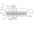
<表示部の構成>
以下、図3及び図4を参照して、表示部11の構成につき説明する。図3は、表示部11の断面構成を示す模式断面図である。図4は、表示部11の回路構成を示す模式回路図である。<Structure of display>
Hereinafter, the configuration of the
図3に示すように、表示部11は、TFT(Thin Film Transistor)液晶パネル21と、光(バックライト)をTFT液晶パネル21の背面に導く導光板27と、TFT液晶パネル21の背面に照射される光(バックライト)を発する光源29と、を備えている。 As shown in FIG. 3, the
TFT液晶パネル21は、上偏光板22と、上ガラス基板23と、液晶層24と、下ガラス基板25と、下偏光板26と、が積層されている。
上偏光板22は、上ガラス基板23の上方に配置された、偏光用の板状部材である。
上ガラス基板23は、液晶層24の上方に配置された、ガラス基板である。
液晶層24は、液晶が封入された層である。
下ガラス基板25は、液晶層24の下方に配置された、ガラス基板である。
下偏光板26は、下ガラス基板25の下方に配置された、偏光用の板状部材である。In the TFT
The upper
The
The
The
The lower
液晶層24は、上ガラス基板23と下ガラス基板25との間に配置されており、シール材28によって封止されている。上ガラス基板23の下面(液晶層24に対向する面)側には、透明電極であるコモン電極23aが配置されている。また、下ガラス基板25の上面(液晶層24に対向する面)側には、透明電極である画素電極25aと、TFT(Thin Film Transistor)25bと、が配置されている。 The
本実施形態では、表示部11のTFT液晶パネル21は、時計ケース1bの内部に収納され、時計ガラス1aで上方をカバーされている。時計ケース1bは、腕時計1の筺体である。時計ガラス1aは、腕時計1のカバー部材である。 In the present embodiment, the TFT
TFT液晶パネル21の下方には、導光板27が配置され、また、導光板27の側方には、バックライト用の光源29が配置されている。光源29は、点灯指示用のスイッチで点灯操作されると、その点灯操作に応答して点灯する。本実施形態では、光源29の点灯指示用のスイッチがプッシュスイッチ4SWであり、光源29の点灯操作がプッシュスイッチ4SWの押下操作であるものとして説明する。そして、光源29は、プッシュスイッチ4SWが押下された場合に、一定時間(例えば、1.5〜3秒間)点灯し、その後に、自動的に消灯する。 A
なお、本実施形態では、1回の点灯操作(1回のプッシュスイッチ4SWの押下操作)における光源29の点灯時間が1.5秒から3秒までの間のいずれかの時間に設定されているとして説明する。しかしながら、1回の点灯操作における光源29の点灯時間はこれに限らない。例えば、点灯時間は、1秒から5秒までの間のいずれかの時間に設定することができる。 In the present embodiment, the lighting time of the
本実施形態に係るTFT液晶パネル21には、低消費電力型のパネルが用いられている。そして、腕時計1は、TFT液晶パネル21のコモン電極23aに入力するコモン信号VCOMの反転周期を長くして(つまり、コモン信号VCOMの周波数を下げて)、コモン信号VCOMの低電流化を図ることにより、低消費電力を実現している。 A low power consumption type panel is used for the TFT
例えば、低消費電力型になっていないTFT液晶パネルでは、コモン信号VCOMの周波数が50〜70Hzの値(例えば、64Hz)になっている。これに対して、低消費電力型になっている本実施形態に係るTFT液晶パネル21では、コモン信号VCOMの周波数が1Hz以下の値(例えば、0.5Hz)になっている。 For example, in a TFT liquid crystal panel that is not a low power consumption type, the frequency of the common signal VCOM is a value of 50 to 70 Hz (for example, 64 Hz). On the other hand, in the TFT
図4に示すように、腕時計1は、表示部11の中に、TFT液晶パネル21と、光源29と、コントローラ31と、信号ドライバ32と、走査ドライバ33と、コモン信号生成部36と、を有している。また、腕時計1は、制御部2の中に検知部37を有している。 As shown in FIG. 4, the
コントローラ31は、水平制御信号を生成して信号ドライバ32に出力するとともに、垂直制御信号を生成して信号ドライバ32に出力する。水平制御信号は、信号ドライバ32の動作を制御する信号である。垂直制御信号は、走査ドライバ33の動作を制御する信号である。 The
また、コントローラ31は、コモン信号生成指示信号を生成して、コモン信号生成部36に出力する。コモン信号生成指示信号は、コモン信号VCOMの生成をコモン信号生成部36に指示する信号である。コモン信号生成部36は、コモン信号生成指示信号に応答してコモン信号VCOMを生成してTFT液晶パネル21のコモン電極23aに出力する。その際に、コモン信号生成部36は、検知部37から後記する停止信号が入力されていなければ、低消費電力に対応したコモン信号VCOMを生成する。一方、コモン信号生成部36は、検知部37から後記する停止信号が入力されていれば、コントラスト差の低減に対応したコモン信号VCOMを生成する。ここで、低消費電力に対応したコモン信号VCOMは、電圧の反転制御が行われた波形の信号である。一方、コントラスト差の低減に対応したコモン信号VCOMは、電圧の反転制御が停止された波形の信号である。 Further, the
信号ドライバ32は、RBG信号をTFT液晶パネル21に出力する。RBG信号は、各画素におけるRBGの階調を表すアナログの電圧信号である。 The
走査ドライバ33は、走査信号(スキャンパルス)を生成してTFT液晶パネル21に出力する。走査信号は、ハイレベル又はローレベルのデジタルの電圧信号である。 The
コモン信号生成部36は、コモン信号VCOMを生成してTFT液晶パネル21のコモン電極23aに出力する。コモン信号VCOMは、ハイレベル又はローレベルのデジタルの電圧信号である。 The common
検知部37は、光源29の点灯操作が検知された場合に、それを検知する機能手段である。検知部37は、光源29の点灯操作が検知された場合に、電圧の反転制御の停止を指示する停止信号を生成してコモン信号生成部36に出力する。この場合に、コモン信号生成部36は、コントラスト差の低減に対応したコモン信号VCOMを生成する。 The
コントローラ31から信号ドライバ32に出力される水平制御信号には、クロック信号や前記したRBG信号、イネーブル信号ENBS等が含まれている。イネーブル信号ENBSは、信号ドライバ32の出力タイミングを制御する信号である。イネーブル信号ENBSは、画像データの水平成分の書き換えを活性化させる水平書き換え活性信号として機能する。 The horizontal control signal output from the
コントローラ31から走査ドライバ33に出力される垂直制御信号には、クロック信号や、イネーブル信号ENBG等が含まれている。イネーブル信号ENBGは、走査ドライバ33の出力タイミングを制御する信号である。イネーブル信号ENBGは、画像データの垂直成分の書き換えを活性化させる垂直書き換え活性信号として機能する。 The vertical control signal output from the
<腕時計の動作>
本実施形態1に係る腕時計1は、光源29の未点灯時と点灯時とで異なる波形のコモン信号VCOMがTFT液晶パネル21のコモン電極23aに入力されるように構成したことを特徴にしている。<Wristwatch operation>
The
以下、図5及び図6を参照して、腕時計1の動作につき説明する。図5は、腕時計1の動作を示す信号波形図である。図6は、腕時計1の動作を示すフローチャートである。 Hereinafter, the operation of the
図5(a)は、光源29の未点灯時における、イネーブル信号ENBG、イネーブル信号ENBS、及びコモン信号VCOMの信号波形を示している。一方、図5(b)は、光源29の点灯時における、イネーブル信号ENBG、イネーブル信号ENBS、及びコモン信号VCOMの信号波形を示している。 FIG. 5A shows the signal waveforms of the enable signal ENBG, the enable signal ENBS, and the common signal VCOM when the
図5(a)に示すように、光源29の未点灯時では、コモン信号VCOMは、ハイレベルとローレベルとが交互に切り替わるように、電圧の反転制御が行われた信号になっている。コモン信号VCOMのハイレベル時間とローレベル時間は、同じになっている。 As shown in FIG. 5A, when the
なお、図5(a)において、時間tcVCOMは、コモン信号VCOMの反転周期を示している。
時間trVCOMは、コモン信号VCOMの立ち上がり時間を示している。
時間tsVCOMは、コモン信号VCOMの立ち上がりが終了してから、TFT液晶パネル21での画像データの書き換えが可能になるまでの設定時間を示している。
時間thVCOMは、TFT液晶パネル21での画像データの書き換えが終了してから、コモン信号VCOMの立ち下がりを開始するまでの設定時間を示している。
時間tfVCOMは、コモン信号VCOMの立ち下がり時間を示している。In FIG. 5A, the time tcVCOM indicates the inversion period of the common signal VCOM.
The time trVCOM indicates the rise time of the common signal VCOM.
The time tsVCOM indicates a set time from the end of the rise of the common signal VCOM to the rewriting of the image data on the TFT
The time thVCOM indicates a set time from the completion of rewriting the image data on the TFT
The time tfVCOM indicates the fall time of the common signal VCOM.
本実施形態では、コモン信号VCOMの反転周期が2秒であるものとして(つまり、コモン信号VCOMの周波数が0.5Hzであるものとして)説明する。 In the present embodiment, it is assumed that the inversion period of the common signal VCOM is 2 seconds (that is, the frequency of the common signal VCOM is 0.5 Hz).
図5(b)に示すように、光源29の点灯時では、コモン信号VCOMは、電圧のハイレベルとローレベルとの反転制御が停止された信号(つまり、0Hzの周波数の信号)になっている。 As shown in FIG. 5B, when the
電圧の反転制御が停止されたコモン信号VCOM(つまり、0Hzの周波数のコモン信号VCOM)は、信号の立ち上がり及び信号の立ち下がりが存在しないため、TFT液晶パネル21に形成された画像のコントラスト差を強調させない信号になっている。 Since the common signal VCOM in which the voltage inversion control is stopped (that is, the common signal VCOM having a frequency of 0 Hz) does not have a signal rise and a signal fall, the contrast difference of the image formed on the TFT
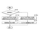
図6に示すように、腕時計1は、表示部11に画像を表示する場合及び表示部11に表示された画像を更新する場合に、ステップS105乃至ステップS125の処理を行う。ここでは、例えば、腕時計1のユーザが、夜中に時刻を確認するために、バックライト用の光源29を点灯させて腕時計1の表示部11に表示された画像を見る場合を想定して説明する。 As shown in FIG. 6, the
まず、検知部37は、光源29の点灯指示用のスイッチであるプッシュスイッチ4SWの状態を監視しており、光源29の点灯操作が検知されたか否かを判定する(ステップS105)。 First, the
ステップS105の判定で、光源29の点灯操作が検知されていない場合(“No”の場合)に、コモン信号生成部36は、ハイレベルとローレベルとが交互に切り替わるように、電圧の反転制御が行われたコモン信号VCOM(図5(a)参照)を生成して、TFT液晶パネル21のコモン電極23aに出力する(ステップS110)。その結果、表示部11は、低消費電力に対応した表示を行う(ステップS115)。 When the lighting operation of the
一方、ステップS105の判定で、光源29の点灯操作が検知された場合(“Yes”の場合)に、コモン信号生成部36は、電圧の反転制御が停止されたコモン信号VCOM(図5(b)参照)を生成して、TFT液晶パネル21のコモン電極23aに出力する(ステップS120)。その結果、表示部11は、コントラスト差低減に対応した表示を行う(ステップS125)。 On the other hand, when the lighting operation of the
なお、本実施形態では、コモン信号VCOMの反転制御の停止時間は、光源29の点灯時間とほぼ同じ時間である1.5〜3秒間(厳密には、若干長い時間)に設定されている。 In the present embodiment, the stop time of the inversion control of the common signal VCOM is set to 1.5 to 3 seconds (strictly speaking, a slightly longer time), which is substantially the same time as the lighting time of the
係る構成において、表示部11のコモン信号生成部36は、光源29の未点灯時に、第1の周波数以下となる低周波数(例えば、1Hz以下となる0.5Hzの周波数)での周期的な電圧の反転制御が行われた信号をコモン信号VCOMとして生成し、一方、光源29の点灯時に、周期的な電圧の反転制御が停止された信号をコモン信号VCOMとして生成する。 In such a configuration, the common
つまり、コモン信号生成部36は、光源29の未点灯時に、低消費電力に対応した波形の信号を生成し、一方、光源29の点灯時に、TFT液晶パネル21に形成された画像のコントラスト差の低減に対応した波形の信号を生成する。 That is, the common
その結果、表示部11は、光源29の未点灯時に、低消費電力に対応した画像表示を行い、一方、光源29の点灯時に、コントラスト差の低減に対応した画像表示を行う。 As a result, the
このような腕時計1は、光源29の点灯時に、光源29から発せられた光(バックライト)でTFT液晶パネル21に形成された画像のコントラスト差が強調されないようにすることができる。そのため、腕時計1は、光源29の点灯時に、TFT液晶パネル21に形成された画像のコントラスト差がユーザに視認されないようにすることができる。その結果、腕時計1は、光源29の点灯時に、ユーザに違和感を与えない画像を表示部11に表示することができる。 In such a
なお、光源29は、一定期間(例えば、6秒)以上連続して点灯すると、輝度が低下することがある。しかしながら、本実施形態では、コモン信号VCOMの反転制御の停止時間がそれよりも短い時間(例えば、1.5〜3秒間)に設定されているため、表示部11に表示される画像は、光源29の輝度の低下による影響を受けることがない。したがって、本実施形態では、表示部11は、コモン信号VCOMの電圧の反転制御を停止しても、光源29の輝度の低下による影響を画像に与えないようにすることができる。 If the
以上の通り、本実施形態1に係る電子装置である腕時計(電子時計)1によれば、光源29の点灯時に、TFT液晶パネル21に形成された画像のコントラスト差がユーザに視認されないようにすることができる。 As described above, according to the wristwatch (electronic clock) 1 which is the electronic device according to the first embodiment, the contrast difference of the image formed on the TFT
[実施形態2]
本実施形態2では、構成自体は前記した実施形態1と同じであるが、コモン信号生成部36の動作が異なる腕時計1を提供する。[Embodiment 2]
In the second embodiment, the
以下、図7及び図8を参照して、本実施形態2の腕時計1の動作につき説明する。図7は、本実施形態2の腕時計1の動作を示す信号波形図である。図8は、本実施形態2の腕時計1の動作を示すフローチャートである。 Hereinafter, the operation of the
ここでは、本実施形態2の動作について、実施形態1と相違する動作を重点的に説明する。したがって、実施形態1と同様の動作(図5及び図6参照)については、前記した実施形態1の動作を本実施形態2の動作に読み替えるものとし、その詳細な説明を省略する。 Here, the operation of the second embodiment will be mainly described as an operation different from that of the first embodiment. Therefore, for the same operation as that of the first embodiment (see FIGS. 5 and 6), the operation of the first embodiment may be replaced with the operation of the second embodiment, and detailed description thereof will be omitted.
図5に示すように、実施形態1では、コモン信号生成部36が、光源29の未点灯時に、1Hz以下の周波数(例えば、0.5Hzの周波数)での電圧の反転制御が行われた信号をコモン信号VCOMとして生成し、一方、光源29の点灯時に、電圧の反転制御が停止された信号をコモン信号VCOMとして生成している。 As shown in FIG. 5, in the first embodiment, the common
これに対し、図7に示すように、本実施形態2では、コモン信号生成部36が、光源29の未点灯時に、1Hz以下の周波数(例えば、0.5Hzの周波数)での電圧の反転制御が行われた信号をコモン信号VCOMとして生成し、一方、光源29の点灯時に、50Hz〜70Hzの周波数(例えば、64Hzの周波数)での電圧の反転制御が行われた信号をコモン信号VCOMとして生成する。 On the other hand, as shown in FIG. 7, in the second embodiment, the common
50Hz〜70Hzの周波数(例えば、64Hzの周波数)での電圧の反転制御が行われたコモン信号VCOMは、信号の立ち上がり及び信号の立ち下がりが画像データの書き換えタイミングに重なり難いため、TFT液晶パネル21に形成された画像のコントラスト差を強調させ難い信号になっている。 In the common signal VCOM in which voltage inversion control is performed at a frequency of 50 Hz to 70 Hz (for example, a frequency of 64 Hz), the rising edge of the signal and the falling edge of the signal do not easily overlap with the rewriting timing of the image data, so that the TFT
図8に示すように、本実施形態2では、実施形態1(図6参照)と同様に、ステップS110の代わりに、ステップS110aの処理を行うとともに、ステップS120の代わりに、ステップS120aの処理を行う点で相違している。 As shown in FIG. 8, in the second embodiment, similarly to the first embodiment (see FIG. 6), the process of step S110a is performed instead of step S110, and the process of step S120a is performed instead of step S120. It differs in what it does.
例えば、本実施形態2では、ステップS110aにおいて、コモン信号生成部36は、第1の周波数以下となる低周波数(例えば、1Hz以下となる0.5Hzの周波数)での電圧の反転制御が行われたコモン信号VCOM(図7(a)参照)を生成して、TFT液晶パネル21のコモン電極23aに出力する。その結果、腕時計1は、ステップS115において、低消費電力に対応した表示を行う。 For example, in the second embodiment, in step S110a, the common
また、本実施形態2では、ステップS120aにおいて、コモン信号生成部36は、第1の周波数より高い第2の周波数以上となる高周波数(例えば、50Hz以上となる64Hzの周波数)での電圧の反転制御が行われたコモン信号VCOM(図7(b)参照)を生成して、TFT液晶パネル21のコモン電極23aに出力する。その結果、腕時計1は、ステップS125において、コントラスト差低減に対応した表示を行う。 Further, in the second embodiment, in step S120a, the common
このような本実施形態2は、実施形態1と同様に、光源29の点灯時に、光源29から発せられた光(バックライト)でTFT液晶パネル21に形成された画像のコントラスト差が強調されないようにすることができる。そのため、本実施形態2は、光源29の点灯時に、TFT液晶パネル21に形成された画像のコントラスト差がユーザに視認されないようにすることができる。 In the second embodiment as in the first embodiment, the contrast difference of the image formed on the TFT
以上の通り、本実施形態2によれば、実施形態1と同様に、光源29の点灯時に、TFT液晶パネル21に形成された画像のコントラスト差がユーザに視認されないようにすることができる。 As described above, according to the second embodiment, it is possible to prevent the user from visually recognizing the contrast difference of the image formed on the TFT
なお、本発明は、前記した実施形態に限定されるものではなく、本発明の要旨を逸脱しない範囲で種々の変更や変形を行うことができる。
例えば、前記した実施形態は、本発明の要旨を分かり易く説明するために詳細に説明したものである。そのため、本発明は、必ずしも説明した全ての構成要素を備えるものに限定されるものではない。また、本発明は、ある構成要素に他の構成要素を追加したり、一部の構成要素を他の構成要素に変更したりすることができる。また、本発明は、一部の構成要素を削除することもできる。The present invention is not limited to the above-described embodiment, and various modifications and modifications can be made without departing from the gist of the present invention.
For example, the above-described embodiment has been described in detail in order to explain the gist of the present invention in an easy-to-understand manner. Therefore, the present invention is not necessarily limited to those including all the components described above. In addition, the present invention can add other components to a certain component, or change some components to other components. In addition, the present invention can also delete some components.
本発明は、腕時計等の電子時計に限らず、表示部での消費電力を低減することが要望されるバッテリ駆動型の電子装置に適用することができる。そのような電子装置としては、腕時計等の電子時計以外に、例えば、ICレコーダーや、体温計、心拍計、満腹計、ビデオカメラ等がある。 The present invention can be applied not only to electronic watches such as wristwatches, but also to battery-powered electronic devices for which it is required to reduce power consumption in the display unit. In addition to electronic clocks such as wristwatches, such electronic devices include, for example, IC recorders, thermometers, heart rate monitors, satiety meters, video cameras, and the like.
以下に、この出願の願書に最初に添付した特許請求の範囲に記載した発明を付記する。付記に記載した請求項の項番は、この出願の願書に最初に添付した特許請求の範囲の通りである。
[付記]
《請求項1》
TFT液晶パネルと、
前記TFT液晶パネルの背面に照射される光を発する光源と、
前記TFT液晶パネルのコモン電極に入力されるコモン信号を生成するコモン信号生成部と、を備え、
前記コモン信号生成部は、前記光源の未点灯時と点灯時とで異なる波形のコモン信号を生成することを特徴とする電子装置。
《請求項2》
請求項1に記載の電子装置において、
前記コモン信号生成部は、前記光源の未点灯時に、第1の周波数以下となる低周波数での周期的な電圧の反転制御が行われた波形の信号を前記コモン信号として生成し、一方、前記光源の点灯時に、周期的な電圧の反転制御が停止された波形の信号を前記コモン信号として生成することを特徴とする電子装置。
《請求項3》
請求項1に記載の電子装置において、
前記コモン信号生成部は、前記光源の未点灯時に、第1の周波数以下となる低周波数での電圧の反転制御が行われた信号を前記コモン信号として生成し、一方、前記光源の点灯時に、前記第1の周波数より高い第2の周波数以上となる高周波数での電圧の反転制御が行われた信号を前記コモン信号として生成することを特徴とする電子装置。
《請求項4》
請求項1から請求項3のいずれか一項に記載の電子装置において、
前記光源の点灯時間は、1秒から5秒までの間のいずれかの時間であることを特徴とする電子装置。
《請求項5》
請求項1から請求項4のいずれか一項に記載の電子装置を備えた電子時計。
《請求項6》
TFT液晶パネルと、前記TFT液晶パネルの背面に照射される光を発する光源と、を備える電子装置の制御部が、前記光源の未点灯時と点灯時とで異なる波形のコモン信号を生成して、前記TFT液晶パネルのコモン電極に出力する工程を含むことを特徴とする表示制御方法。
《請求項7》
TFT液晶パネルと、前記TFT液晶パネルの背面に照射される光を発する光源と、を備える電子装置の制御部に、前記光源の未点灯時と点灯時とで異なる波形のコモン信号を生成させて、前記TFT液晶パネルのコモン電極に出力させる工程を行わせるプログラム。The inventions described in the claims originally attached to the application of this application are added below. The claims in the appendix are as specified in the claims originally attached to the application for this application.
[Additional Notes]
<< Claim 1 >>
TFT liquid crystal panel and
A light source that emits light emitted from the back surface of the TFT liquid crystal panel,
A common signal generation unit that generates a common signal input to the common electrode of the TFT liquid crystal panel is provided.
The common signal generation unit is an electronic device that generates a common signal having different waveforms when the light source is not lit and when the light source is lit.
<< Claim 2 >>
In the electronic device according to
The common signal generation unit generates as the common signal a signal having a waveform in which periodic voltage inversion control is performed at a low frequency lower than the first frequency when the light source is not lit. An electronic device characterized in that when a light source is turned on, a signal having a waveform in which periodic voltage inversion control is stopped is generated as the common signal.
<< Claim 3 >>
In the electronic device according to
The common signal generation unit generates a signal in which voltage inversion control is performed at a low frequency lower than the first frequency when the light source is not lit, as the common signal, while when the light source is lit, the common signal generation unit generates a signal. An electronic device characterized in that a signal in which voltage inversion control is performed at a high frequency higher than the first frequency and higher than the second frequency is generated as the common signal.
<< Claim 4 >>
In the electronic device according to any one of
An electronic device characterized in that the lighting time of the light source is any time between 1 second and 5 seconds.
<< Claim 5 >>
An electronic clock provided with the electronic device according to any one of
<< Claim 6 >>
A control unit of an electronic device including a TFT liquid crystal panel and a light source that emits light emitted from the back surface of the TFT liquid crystal panel generates a common signal having a different waveform when the light source is not lit and when the light source is lit. , A display control method comprising a step of outputting to a common electrode of the TFT liquid crystal panel.
<< Claim 7 >>
A control unit of an electronic device including a TFT liquid crystal panel and a light source that emits light emitted from the back surface of the TFT liquid crystal panel is made to generate a common signal having different waveforms when the light source is not lit and when the light source is lit. , A program for performing a step of outputting to the common electrode of the TFT liquid crystal panel.
1 腕時計(電子装置の一例としての電子時計)
1a 時計ケース(筐体)
1b 時計ガラス(カバー部材)
2 制御部
3 記憶部
4 通信部
5 GPSレシーバ
6 磁気センサ
7 計時回路
11 表示部
21 TFT液晶パネル
22 上偏光板
23 上ガラス基板
23a コモン電極
24 液晶層
25 下ガラス基板
25a 画素電極
25b TFT
26 下偏光板
27 導光板
28 シール材
29 LED(光源)
31 コントローラ
32 信号ドライバ
33 走査ドライバ
36 コモン信号生成部
37 検知部
RSW ロータリーSW
1SW,2SW,3SW,4SW プッシュSW1 Wristwatch (electronic clock as an example of an electronic device)
1a Watch case (housing)
1b Watch glass (cover member)
2
26
31
1SW, 2SW, 3SW, 4SW Push SW
Claims (8)
Translated fromJapanese前記TFT液晶パネルの背面に照射される光を発する光源と、
前記TFT液晶パネルのコモン電極に入力されるコモン信号を生成するコモン信号生成部と、を備え、
前記コモン信号生成部は、前記光源の未点灯時に、第1の周波数以下となる低周波数での周期的な電圧の反転制御が行われた波形の信号を前記コモン信号として生成し、一方、前記光源の点灯時に、周期的な電圧の反転制御が停止された波形の信号を前記コモン信号として生成することを特徴とする電子装置。TFT liquid crystal panel and
A light source that emits light emitted from the back surface of the TFT liquid crystal panel,
A common signal generation unit that generates a common signal input to the common electrode of the TFT liquid crystal panel is provided.
The common signal generation unitgenerates as the common signal a signal having a waveform in which periodic voltage inversion control is performed at a low frequency lower than the first frequency when the light source is not lit. An electronic device characterizedin that when a light source is turned on, a signal having a waveform in which periodic voltage inversion control is stopped is generated as the common signal .
前記TFT液晶パネルの背面に照射される光を発する光源と、 A light source that emits light emitted from the back surface of the TFT liquid crystal panel,
前記TFT液晶パネルのコモン電極に入力されるコモン信号を生成するコモン信号生成部と、を備え、 A common signal generation unit that generates a common signal input to the common electrode of the TFT liquid crystal panel is provided.
前記コモン信号生成部は、前記光源の未点灯時に、第1の周波数以下となる低周波数での電圧の反転制御が行われた信号を前記コモン信号として生成し、一方、前記光源の点灯時に、前記第1の周波数より高い第2の周波数以上となる高周波数での電圧の反転制御が行われた信号を前記コモン信号として生成することを特徴とする電子装置。 The common signal generation unit generates a signal in which voltage inversion control is performed at a low frequency lower than the first frequency when the light source is not lit, as the common signal, while when the light source is lit, the common signal generation unit generates a signal. An electronic device characterized in that a signal in which voltage inversion control is performed at a high frequency higher than the first frequency and higher than the second frequency is generated as the common signal.
前記光源の点灯時間は、1秒から5秒までの間のいずれかの時間であることを特徴とする電子装置。In the electronic device accordingto claim1 or 2 .
An electronic device characterized in that the lighting time of the light source is any time between 1 second and 5 seconds.
Priority Applications (3)
| Application Number | Priority Date | Filing Date | Title |
|---|---|---|---|
| JP2017213585AJP6801630B2 (en) | 2017-11-06 | 2017-11-06 | Electronic devices, electronic clocks, display control methods, and programs |
| US16/180,348US10824117B2 (en) | 2017-11-06 | 2018-11-05 | Electronic device, electronic timepiece, display control method, and storage medium |
| CN201811312826.6ACN109754765B (en) | 2017-11-06 | 2018-11-06 | Electronic device, electronic clock, display control method, and storage medium |
Applications Claiming Priority (1)
| Application Number | Priority Date | Filing Date | Title |
|---|---|---|---|
| JP2017213585AJP6801630B2 (en) | 2017-11-06 | 2017-11-06 | Electronic devices, electronic clocks, display control methods, and programs |
Publications (2)
| Publication Number | Publication Date |
|---|---|
| JP2019086610A JP2019086610A (en) | 2019-06-06 |
| JP6801630B2true JP6801630B2 (en) | 2020-12-16 |
Family
ID=66327211
Family Applications (1)
| Application Number | Title | Priority Date | Filing Date |
|---|---|---|---|
| JP2017213585AActiveJP6801630B2 (en) | 2017-11-06 | 2017-11-06 | Electronic devices, electronic clocks, display control methods, and programs |
Country Status (3)
| Country | Link |
|---|---|
| US (1) | US10824117B2 (en) |
| JP (1) | JP6801630B2 (en) |
| CN (1) | CN109754765B (en) |
Families Citing this family (1)
| Publication number | Priority date | Publication date | Assignee | Title |
|---|---|---|---|---|
| US11676554B2 (en)* | 2021-05-10 | 2023-06-13 | Dell Products L.P. | Optimizing flickering of a liquid crystal display |
Family Cites Families (14)
| Publication number | Priority date | Publication date | Assignee | Title |
|---|---|---|---|---|
| FR2722603B1 (en)* | 1994-07-12 | 1996-09-27 | Sagem | LIQUID CRYSTAL, ACTIVE MATRIX AND FRACTIONAL COUNTER ELECTRODE DISPLAY DEVICE |
| US6545654B2 (en)* | 1996-10-31 | 2003-04-08 | Kopin Corporation | Microdisplay for portable communication systems |
| JP2003280601A (en) | 2002-03-20 | 2003-10-02 | Matsushita Electric Ind Co Ltd | Liquid crystal display |
| TW564390B (en)* | 2002-09-16 | 2003-12-01 | Au Optronics Corp | Driving circuit and method for light emitting device |
| GB2403841B (en)* | 2003-07-07 | 2006-08-09 | Pelikon Ltd | Control of Electroluminescent displays |
| JP2008224924A (en)* | 2007-03-12 | 2008-09-25 | Seiko Epson Corp | Liquid crystal device, driving method thereof, and electronic apparatus |
| JP2010164844A (en)* | 2009-01-16 | 2010-07-29 | Nec Lcd Technologies Ltd | Liquid crystal display device, driving method used for the liquid crystal display device, and integrated circuit |
| US20120086741A1 (en)* | 2009-07-01 | 2012-04-12 | Sharp Kabushiki Kaisha | Image Display Device |
| JP5257346B2 (en) | 2009-12-08 | 2013-08-07 | カシオ計算機株式会社 | Liquid crystal display device, electronic device, liquid crystal display driving device, and liquid crystal display driving method |
| JP2013205688A (en) | 2012-03-29 | 2013-10-07 | Nitto Denko Corp | Liquid crystal display device |
| JP2014048240A (en) | 2012-09-03 | 2014-03-17 | Seiko Instruments Inc | Electronic clock and program |
| WO2014045749A1 (en)* | 2012-09-21 | 2014-03-27 | シャープ株式会社 | Display control system, processor, controller, and display control method |
| KR102073685B1 (en)* | 2013-09-06 | 2020-02-06 | 삼성디스플레이 주식회사 | Liquid crystal display device |
| US20190094590A1 (en)* | 2016-03-07 | 2019-03-28 | Sharp Kabushiki Kaisha | Liquid crystal display device with built-in touch sensor, and drive method therefor |
- 2017
- 2017-11-06JPJP2017213585Apatent/JP6801630B2/enactiveActive
- 2018
- 2018-11-05USUS16/180,348patent/US10824117B2/enactiveActive
- 2018-11-06CNCN201811312826.6Apatent/CN109754765B/enactiveActive
Also Published As
| Publication number | Publication date |
|---|---|
| CN109754765B (en) | 2021-08-24 |
| JP2019086610A (en) | 2019-06-06 |
| US20190137944A1 (en) | 2019-05-09 |
| US10824117B2 (en) | 2020-11-03 |
| CN109754765A (en) | 2019-05-14 |
Similar Documents
| Publication | Publication Date | Title |
|---|---|---|
| US11079835B2 (en) | Display device and method for controlling same | |
| JP6866584B2 (en) | Display device, display control method and program | |
| US10706491B2 (en) | Display device with multi-processor, control method for the same, and storage medium having control program stored thereon | |
| US8044927B2 (en) | Drive method for a display device, drive device, display device, and electronic device | |
| US11048109B2 (en) | Display module, display device, and method for controlling same | |
| JP2019007751A (en) | Wearable device and method for controlling the same | |
| US9564087B2 (en) | Electrophoretic display device, electronic timepiece, and operating method of an electrophoretic display device | |
| JP2008209893A (en) | Display device driving method, driving device, display device, and electronic apparatus | |
| US20150323906A1 (en) | Timepiece and power saving method thereof | |
| JP6801630B2 (en) | Electronic devices, electronic clocks, display control methods, and programs | |
| JP2012189531A (en) | Electronic clock | |
| JP2015137939A (en) | electronic watch | |
| US9411319B1 (en) | Electronic apparatus | |
| JP2015138119A (en) | Arm-attaching electronic apparatus | |
| JP2007047991A (en) | Display device and display method | |
| JP6439827B2 (en) | Display device, control method therefor, and control program | |
| US10783845B2 (en) | Liquid crystal control circuit, electronic timepiece, and liquid crystal control method | |
| JP7187792B2 (en) | ELECTRONIC DEVICE, ELECTRONIC CLOCK, LIQUID CRYSTAL CONTROL METHOD AND PROGRAM | |
| JP2008157889A (en) | Portable information equipment | |
| JP6288425B2 (en) | Watches | |
| JP2008040203A (en) | Electro-optic device and electronic equipment | |
| JP2011166349A (en) | Radio wave receiver, radio wave wrist watch, radio wave receiving equipment, and radio wave receiving control method |
Legal Events
| Date | Code | Title | Description |
|---|---|---|---|
| A621 | Written request for application examination | Free format text:JAPANESE INTERMEDIATE CODE: A621 Effective date:20191017 | |
| A131 | Notification of reasons for refusal | Free format text:JAPANESE INTERMEDIATE CODE: A131 Effective date:20200804 | |
| A521 | Written amendment | Free format text:JAPANESE INTERMEDIATE CODE: A523 Effective date:20201001 | |
| TRDD | Decision of grant or rejection written | ||
| A01 | Written decision to grant a patent or to grant a registration (utility model) | Free format text:JAPANESE INTERMEDIATE CODE: A01 Effective date:20201027 | |
| A61 | First payment of annual fees (during grant procedure) | Free format text:JAPANESE INTERMEDIATE CODE: A61 Effective date:20201109 | |
| R150 | Certificate of patent or registration of utility model | Ref document number:6801630 Country of ref document:JP Free format text:JAPANESE INTERMEDIATE CODE: R150 |