JP6783573B2 - Display device - Google Patents
Display deviceDownload PDFInfo
- Publication number
- JP6783573B2 JP6783573B2JP2016144198AJP2016144198AJP6783573B2JP 6783573 B2JP6783573 B2JP 6783573B2JP 2016144198 AJP2016144198 AJP 2016144198AJP 2016144198 AJP2016144198 AJP 2016144198AJP 6783573 B2JP6783573 B2JP 6783573B2
- Authority
- JP
- Japan
- Prior art keywords
- insulating layer
- display device
- density
- region
- pattern
- Prior art date
- Legal status (The legal status is an assumption and is not a legal conclusion. Google has not performed a legal analysis and makes no representation as to the accuracy of the status listed.)
- Active
Links
Images


Classifications
- H—ELECTRICITY
- H10—SEMICONDUCTOR DEVICES; ELECTRIC SOLID-STATE DEVICES NOT OTHERWISE PROVIDED FOR
- H10K—ORGANIC ELECTRIC SOLID-STATE DEVICES
- H10K77/00—Constructional details of devices covered by this subclass and not covered by groups H10K10/80, H10K30/80, H10K50/80 or H10K59/80
- H10K77/10—Substrates, e.g. flexible substrates
- H10K77/111—Flexible substrates
- H—ELECTRICITY
- H10—SEMICONDUCTOR DEVICES; ELECTRIC SOLID-STATE DEVICES NOT OTHERWISE PROVIDED FOR
- H10K—ORGANIC ELECTRIC SOLID-STATE DEVICES
- H10K50/00—Organic light-emitting devices
- H10K50/80—Constructional details
- H10K50/84—Passivation; Containers; Encapsulations
- H10K50/844—Encapsulations
- H—ELECTRICITY
- H10—SEMICONDUCTOR DEVICES; ELECTRIC SOLID-STATE DEVICES NOT OTHERWISE PROVIDED FOR
- H10K—ORGANIC ELECTRIC SOLID-STATE DEVICES
- H10K59/00—Integrated devices, or assemblies of multiple devices, comprising at least one organic light-emitting element covered by group H10K50/00
- H—ELECTRICITY
- H10—SEMICONDUCTOR DEVICES; ELECTRIC SOLID-STATE DEVICES NOT OTHERWISE PROVIDED FOR
- H10K—ORGANIC ELECTRIC SOLID-STATE DEVICES
- H10K71/00—Manufacture or treatment specially adapted for the organic devices covered by this subclass
- H—ELECTRICITY
- H10—SEMICONDUCTOR DEVICES; ELECTRIC SOLID-STATE DEVICES NOT OTHERWISE PROVIDED FOR
- H10K—ORGANIC ELECTRIC SOLID-STATE DEVICES
- H10K2102/00—Constructional details relating to the organic devices covered by this subclass
- H10K2102/301—Details of OLEDs
- H10K2102/311—Flexible OLED
- H—ELECTRICITY
- H10—SEMICONDUCTOR DEVICES; ELECTRIC SOLID-STATE DEVICES NOT OTHERWISE PROVIDED FOR
- H10K—ORGANIC ELECTRIC SOLID-STATE DEVICES
- H10K59/00—Integrated devices, or assemblies of multiple devices, comprising at least one organic light-emitting element covered by group H10K50/00
- H10K59/80—Constructional details
- H10K59/87—Passivation; Containers; Encapsulations
- H10K59/873—Encapsulations
- Y—GENERAL TAGGING OF NEW TECHNOLOGICAL DEVELOPMENTS; GENERAL TAGGING OF CROSS-SECTIONAL TECHNOLOGIES SPANNING OVER SEVERAL SECTIONS OF THE IPC; TECHNICAL SUBJECTS COVERED BY FORMER USPC CROSS-REFERENCE ART COLLECTIONS [XRACs] AND DIGESTS
- Y02—TECHNOLOGIES OR APPLICATIONS FOR MITIGATION OR ADAPTATION AGAINST CLIMATE CHANGE
- Y02E—REDUCTION OF GREENHOUSE GAS [GHG] EMISSIONS, RELATED TO ENERGY GENERATION, TRANSMISSION OR DISTRIBUTION
- Y02E10/00—Energy generation through renewable energy sources
- Y02E10/50—Photovoltaic [PV] energy
- Y02E10/549—Organic PV cells
- Y—GENERAL TAGGING OF NEW TECHNOLOGICAL DEVELOPMENTS; GENERAL TAGGING OF CROSS-SECTIONAL TECHNOLOGIES SPANNING OVER SEVERAL SECTIONS OF THE IPC; TECHNICAL SUBJECTS COVERED BY FORMER USPC CROSS-REFERENCE ART COLLECTIONS [XRACs] AND DIGESTS
- Y02—TECHNOLOGIES OR APPLICATIONS FOR MITIGATION OR ADAPTATION AGAINST CLIMATE CHANGE
- Y02P—CLIMATE CHANGE MITIGATION TECHNOLOGIES IN THE PRODUCTION OR PROCESSING OF GOODS
- Y02P70/00—Climate change mitigation technologies in the production process for final industrial or consumer products
- Y02P70/50—Manufacturing or production processes characterised by the final manufactured product
Landscapes
- Engineering & Computer Science (AREA)
- Manufacturing & Machinery (AREA)
- Physics & Mathematics (AREA)
- Optics & Photonics (AREA)
- Electroluminescent Light Sources (AREA)
- Devices For Indicating Variable Information By Combining Individual Elements (AREA)
Description
Translated fromJapanese有機エレクトロルミネッセンス(以下、有機ELと呼ぶ。)表示装置は、各画素に発光素子が設けられ、個別に発光を制御することで画像を表示する。発光素子は、一方をアノード、他方をカソードとして区別される一対の電極間に有機EL材料を含む層(以下、「発光層」ともいう)を挟んだ構造を有している。発光層に、カソードから電子が注入され、アノードから正孔が注入されると、電子と正孔が再結合する。これにより放出される余剰なエネルギーによって発光層中の発光分子が励起し、その後脱励起することによって発光する。 In an organic electroluminescence (hereinafter referred to as organic EL) display device, a light emitting element is provided for each pixel, and an image is displayed by individually controlling light emission. The light emitting device has a structure in which a layer containing an organic EL material (hereinafter, also referred to as “light emitting layer”) is sandwiched between a pair of electrodes that are distinguished by one as an anode and the other as a cathode. When electrons are injected from the cathode and holes are injected from the anode into the light emitting layer, the electrons and holes are recombined. The surplus energy emitted by this excites the luminescent molecules in the light emitting layer, and then deexcites them to emit light.
有機EL表示装置においては、発光素子の各々のアノードは画素毎に画素電極として設けられ、カソードは複数の画素に跨がって共通の電位が印加される共通電極として設けられている。有機EL表示装置は、この共通電極の電位に対し、画素電極の電位を画素毎に印加することで、画素の発光を制御している。尚、カソードは各画素毎に設けられてもよく、この場合は必ずしもすべての画素で共通の電位にしなくてもよい。 In the organic EL display device, each anode of the light emitting element is provided as a pixel electrode for each pixel, and the cathode is provided as a common electrode to which a common potential is applied across a plurality of pixels. The organic EL display device controls the light emission of pixels by applying the potential of the pixel electrode to the potential of the common electrode for each pixel. The cathode may be provided for each pixel, and in this case, the potential does not necessarily have to be common to all the pixels.
しかしながら、有機EL表示装置の発光層は、水分が侵入すると容易に劣化し、ダークスポットと呼ばれる非点灯領域が発生してしまうという課題がある。このような課題を解決するため、多くの有機EL表示装置には、水分の侵入を防止するための封止層が設けられている。 However, there is a problem that the light emitting layer of the organic EL display device is easily deteriorated when moisture invades, and a non-lighting region called a dark spot is generated. In order to solve such a problem, many organic EL display devices are provided with a sealing layer for preventing the intrusion of moisture.
例えば特許文献1には、基板と、基板上に形成されたディスプレイ部と、ディスプレイ部と前記ディスプレイ部周辺の非発光領域とを覆い、中央部からエッジ部に行くほど密度及び厚さが増大する封止膜と、を備える有機発光ディスプレイ装置が開示されている。これにより、側面方向の水分や酸素の浸透を防止して有機発光ディスプレイ装置の寿命を延長させうる。 For example, in Patent Document 1, the substrate, the display portion formed on the substrate, the display portion, and the non-light emitting region around the display portion are covered, and the density and thickness increase from the central portion to the edge portion. An organic light emitting display device including a sealing film is disclosed. As a result, it is possible to prevent the permeation of water and oxygen in the lateral direction and extend the life of the organic light emitting display device.
近年、表示領域が折り曲げ可能なフレキシブル表示装置が盛んに開発されている。フレキシブル表示装置に設けられた封止層は、高密度にするとバリア性が高まる反面、折り曲げた際にクラックが生じ易くなるという課題がある。封止層に生じたクラックは水分の侵入経路となり得ることから、表示装置の信頼性が低下してしまう。 In recent years, flexible display devices having a bendable display area have been actively developed. The sealing layer provided in the flexible display device has a problem that cracks are likely to occur when it is bent, while the barrier property is enhanced when the density is increased. Since the cracks generated in the sealing layer can serve as a passage for moisture to enter, the reliability of the display device is lowered.
本発明は、表示装置の折り曲げ時に、封止層にクラックが生じにくく、高い信頼性を有する表示装置を提供することを目的の一つとする。 One of the objects of the present invention is to provide a display device having high reliability in which cracks are less likely to occur in the sealing layer when the display device is bent.
本発明の一実施形態に係る表示装置は、表示領域に複数の画素が配列されたアレイ基板と、前記複数の画素を覆う封止層とを備え、前記封止層は、疎密パターンを有する絶縁層を含み、前記疎密パターンは、低密度領域及び高密度領域を含むパターンであり、前記低密度領域は、前記絶縁層の前記表示領域内の平均密度よりも前記絶縁層の密度が低い領域であり、前記高密度領域は、前記絶縁層の前記表示領域内の平均密度よりも前記絶縁層の密度が高い領域であることを特徴とする。 The display device according to the embodiment of the present invention includes an array substrate in which a plurality of pixels are arranged in a display area and a sealing layer covering the plurality of pixels, and the sealing layer is an insulating having a sparse and dense pattern. The sparse and dense pattern including layers is a pattern including a low density region and a high density region, and the low density region is a region where the density of the insulating layer is lower than the average density in the display region of the insulating layer. The high-density region is characterized in that the density of the insulating layer is higher than the average density of the insulating layer in the display region.
本発明の一実施形態に係る表示装置の製造方法は、表示領域に複数の画素が配列されたアレイ基板を準備し、所定のパターンを有する温度勾配を有する基板保持体に前記アレイ基板を設置し、前記複数の画素上に、前記所定のパターンに対応した疎密パターンを有する無機絶縁層を成膜することを含み、前記疎密パターンは、低密度領域及び高密度領域が繰り返し配置されるパターンであり、前記低密度領域は、前記無機絶縁層の前記表示領域の平均密度よりも前記無機絶縁層の密度が低い領域であり、前記高密度領域は、前記無機絶縁層の前記表示領域の平均密度よりも前記無機絶縁層の密度が高い領域であることを特徴とする。 In the method for manufacturing a display device according to an embodiment of the present invention, an array substrate in which a plurality of pixels are arranged in a display region is prepared, and the array substrate is placed on a substrate holder having a temperature gradient having a predetermined pattern. Including forming an inorganic insulating layer having a sparse and dense pattern corresponding to the predetermined pattern on the plurality of pixels, the sparse and dense pattern is a pattern in which a low density region and a high density region are repeatedly arranged. The low-density region is a region where the density of the inorganic insulating layer is lower than the average density of the display region of the inorganic insulating layer, and the high-density region is higher than the average density of the display region of the inorganic insulating layer. Is also characterized in that it is a region where the density of the inorganic insulating layer is high.
以下、図面を参照して、本発明のいくつかの実施形態に係る表示装置について詳細に説明する。なお、本発明の表示装置は以下の実施形態に限定されることはなく、種々の変形を行ない実施することが可能である。全ての実施形態においては、同じ構成要素には同一符号を付して説明する。また、図面の寸法比率は、説明の都合上、実際の比率とは異なったり、構成の一部が図面から省略されたりする場合がある。 Hereinafter, the display device according to some embodiments of the present invention will be described in detail with reference to the drawings. The display device of the present invention is not limited to the following embodiments, and can be modified in various ways. In all embodiments, the same components are designated by the same reference numerals. Further, the dimensional ratio of the drawing may differ from the actual ratio for convenience of explanation, or a part of the configuration may be omitted from the drawing.
<第1実施形態>
[外観の構成]
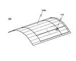
図1は、本実施形態に係る表示装置100の外観の構成を説明する斜視図である。図1を用いて、本実施形態に係る表示装置100の外観の構成について説明する。<First Embodiment>
[Appearance composition]
FIG. 1 is a perspective view illustrating an external configuration of the
本実施形態に係る表示装置100は、アレイ基板102と、対向基板106と、複数の接続端子109とを有している。 The
アレイ基板102は、少なくとも第1基板104及び複数の画素110を有している。 The
第1基板104は、可撓性を有している。可撓性を有する基板の材料としては、具体的な材料は後述するが、樹脂材料が用いられる。第1基板104上には、表示領域104a及び端子領域104bが設けられている。 The
複数の画素110は、第1基板104の表示領域104a内に配列されている。本実施形態においては、複数の画素110は、行列状に配列されている。複数の画素110の各々は、図1には示されていないが、少なくとも選択トランジスタ、駆動トランジスタ及び発光素子を有する画素回路から構成される。 The plurality of
対向基板106は、少なくとも第2基板108を有している。 The facing
第2基板108は、可撓性を有している。可撓性を有する基板としては、第1基板104と同様の基板を用いることができる。第2基板108は、表示領域104aの上面に、第1基板104と対向するように設けられている。第2基板108は表示領域104aを囲むシール材130によって、第1基板104に固定されている。第1基板104に配置された表示領域104aは、第2基板108とシール材130とによって大気に晒されないように封止されている。このような封止構造により、複数の画素110の各々が有する発光素子の劣化を抑制している。 The
対向基板106は、カラーフィルタ、遮光層、偏光板、位相板等を更に有していてもよい。 The facing
カラーフィルタは、複数の画素110の各々に対向した位置に配置される。遮光層(ブラックマトリクスとも呼ばれる)は、複数の画素110の各々を区画する位置に配置される。 The color filter is arranged at a position facing each of the plurality of
偏光板及び位相板は、複数の画素110を覆い、対向基板106側に配置される。偏光板及び位相板は、表示装置100に入射した外光が、画素電極で反射することによる視認性の劣化を抑制するために配置される。 The polarizing plate and the phase plate cover the plurality of
複数の接続端子109は、端子領域104b内に設けられている。複数の端子領域104bは、第1基板104の一端部、且つ第2基板108の外側に配置されている。複数の接続端子109には、映像信号を出力する機器や電源などと表示装置100とを接続する配線基板(図示せず)が配置される。配線基板と接続する複数の接続端子109との接点は、外部に露出している。 The plurality of
以上、本実施形態に係る表示装置100の外観の構成について説明した。次いで、図面を参照して本実施形態に係る表示装置100の詳細な構成について説明する。 The configuration of the appearance of the
[構成の詳細]
図2Aは、本実施形態に係る表示装置100の概略構成を説明する平面図及び断面図である。図2Bは、本実施形態に係る表示装置100を折り曲げた状態を説明する斜視図である。図3は、本実施形態に係る表示装置100の構成を説明する拡大断面図である。後述するが、表示領域は、低密度領域126a及び高密度領域126bを有している。図3において、上段には表示装置100の低密度領域126aの断面図、下段には表示装置100の高密度領域126bの断面図を示している。[Details of configuration]
FIG. 2A is a plan view and a cross-sectional view illustrating a schematic configuration of the
本実施形態に係る表示装置100は、アレイ基板102と、封止層120とを備えている。 The
アレイ基板102は、第1基板104及び複数の画素110を有している。 The
第1基板104は、表示領域140a及び端子領域140bを有している。第1基板104は、本実施形態においては、可撓性を有する基板が用いられる。可撓性を有する基板としては、樹脂材料が用いられる。樹脂材料としては、繰り返し単位にイミド結合を含む高分子材料を用いるのが好ましく、例えば、ポリイミドが用いられる。具体的には、第1基板104として、ポリイミドをシート状に成形したフィルム基板が用いられる。これによって、アレイ基板102は、全体として可撓性を有する。 The
複数の画素110の各々は、第1基板104上の表示領域140aに配列されている。複数の画素110の各々は、少なくとも選択トランジスタ(図示せず)、駆動トランジスタ(図示せず)及び発光素子112を有する画素回路から構成される。 Each of the plurality of
発光素子112としては、自発光型の発光素子112を用いることができ、例えば有機EL発光素子を用いることができる。有機EL発光素子は、画素電極114、共通電極116及び発光層118を有している。 As the
画素電極114は、複数の画素110の各々に対して配置されている。画素電極114の材料としては、発光層118で発生した光を共通電極116側に反射させるために、反射率の高い金属層を含むことが好ましい。反射率の高い金属層としては、例えば銀(Ag)を用いることができる。 The
更に、前述の反射率の高い金属層に加え、透明導電層が積層されてもよい。透明導電層としては、透光性を有し、且つ導電性を有するITO(酸化スズ添加酸化インジウム)やIZO(酸化インジウム・酸化亜鉛)等を用いることが好ましい。また、それらの任意の組み合わせを用いてもよい。 Further, in addition to the above-mentioned metal layer having high reflectance, a transparent conductive layer may be laminated. As the transparent conductive layer, it is preferable to use ITO (tin oxide-added indium oxide), IZO (indium oxide / zinc oxide), etc., which have translucency and conductivity. Moreover, you may use any combination thereof.
本実施例で共通電極116は、複数の画素110に亘って配置されている。共通電極116の材料としては、発光層118で発生した光を透過させるために、透光性を有し、且つ導電性を有するITO(酸化スズ添加酸化インジウム)やIZO(酸化インジウム・酸化亜鉛)等が好ましい。又は、共通電極116として、出射光が透過できる程度の膜厚を有する金属層を用いても良い。なお共通電極は各画素電極毎に個別に形成されることがあってもよい。 In this embodiment, the
発光層118は、画素電極114及び共通電極116に挟持されて配置されている。発光層118の材料としては、電流が供給されると発光する有機EL材料である。有機EL材料としては、低分子系又は高分子系の有機材料を用いることができる。低分子系の有機材料を用いる場合、発光層118は発光性の有機材料に加え、発光性の有機材料を挟持するように正孔注入層や電子注入層、更に正孔輸送層や電子輸送層等を含んで構成される。 The
隣接する2つの画素110間には、バンク128が設けられている。バンク128は、画素電極114の周縁部を覆うように設けられている。 A
バンク128の材料としては、絶縁材料を用いることが好ましい。絶縁材料としては、無機絶縁材料又は有機絶縁材料を用いることができる。無機絶縁材料としては、例えば酸化珪素、窒化珪素、又はそれらの組み合わせ等を用いることができる。有機絶縁材料としては、例えばポリイミド樹脂、アクリル樹脂、又はそれらの組み合わせ等を用いることができる。無機絶縁材料と有機絶縁材料との組み合わせを用いてもよい。 As the material of the
絶縁材料で形成されたバンク128が配置されることによって、画素電極114の端部において、共通電極116と画素電極114とが短絡することを防止することができる。更に、隣接する画素110間を確実に絶縁することができる。 By arranging the
封止層120は、表示領域140aに亘って配置され、複数の画素110を覆っている。 The
本実施形態においては、封止層120は、第1絶縁層122、第2絶縁層124b及び第3絶縁層126を含んでいる。封止層120を構成するこれらの層は、下層から、第1絶縁層122、第2絶縁層124、そして第3絶縁層126の順で積層されている。これらの層について、下層側から順に説明する。 In the present embodiment, the
第1絶縁層122は、封止層120において最下層に配置されている。第1絶縁層122の材料としては、透湿性の低い絶縁材料が好ましい。 The first insulating
第1絶縁層122の具体的な材料としては、無機絶縁層を用いることができる。無機絶縁層の具体的な材料としては、例えば、酸化珪素(SiOx)、窒化珪素(SiNx)、酸化窒化珪素(SiOxNy)、窒化酸化珪素(SiNxOy)、酸化アルミニウム(AlOx)、窒化アルミニウム(AlNx)、酸化窒化アルミニウム(AlOxNy)、窒化酸化アルミニウム(AlNxOy)等の層を使用することができる(x、yは任意)。また、これらの層を積層した構造を使用してもよい。本実施形態においては、第1絶縁層122の材料として窒化珪素を用いる。 As a specific material of the first insulating
第2絶縁層124は、第1絶縁層122の上に配置されている。第2絶縁層124の材料としては、下層に配置された複数の発光素子112やバンク128等に起因する凹凸を平坦化できる絶縁材料が好ましい。そのような凹凸が存在すると、第1絶縁層122の被覆性が十分ではなく、第1絶縁層122に水分の伝搬経路が発生する場合がある。 The second
第2絶縁層124の具体的な材料としては、無機絶縁層又は有機絶縁層を用いることができる。無機絶縁層としては、前述の無機絶縁層を用いることができる。有機絶縁層としては、例えば、アクリル樹脂、エポキシ樹脂等を用いることができる。 As a specific material of the second insulating
本実施形態においては、第2絶縁層124の材料としてはアクリル樹脂を用いる。 In the present embodiment, acrylic resin is used as the material of the second insulating
第3絶縁層126は、第2絶縁層124の上に配置されている。第3絶縁層126の材料としては、透湿性の低い絶縁材料が好ましい。本実施形態においては第2絶縁層124としてアクリル樹脂を用いるが、有機絶縁層は水分の侵入経路となりやすい。そのため、第2絶縁層124に水分が侵入すると、第1絶縁層122に到達し、更に発光層118に侵入してしまうことが懸念される。アクリル樹脂を用いた第2絶縁層124は高い平坦性を有するため、第3絶縁層126は被覆性に優れ、そのため水分の伝搬経路が発生しにくい。 The third
本実施形態においては、第3絶縁層126の材料として窒化珪素を用いる。 In this embodiment, silicon nitride is used as the material of the third insulating
第3絶縁層126は、更に、疎密パターンを有している。ここで、疎密パターンとは、低密度領域126a及び高密度領域126bを含むパターンである。当該パターンは、周期的なパターンであってもよい。低密度領域126aとは、表示領域内に亘って配置された第3絶縁層126の平均密度よりも第3絶縁層126の密度が低い領域である。高密度領域126bとは、表示領域内に亘って配置された第3絶縁層126の平均密度よりも第3絶縁層126の密度が高い領域である。ここで、密度とは、面積密度(単位はatoms/cm2)を意味してもよく、体積密度(単位はatoms/cm3)を意味してもよい。さらに水素含有量が変化する場合も含む。The third
尚、疎密パターンは、低密度領域126a及び高密度領域126bの境界近傍において、それぞれの領域内の局所的な密度分布が、ほぼ階段状に変化する明確なコントラストを有するとは限らない。よって、疎密パターンとは、例えば密度分布が正弦波状に変化する場合も含む。 The sparse and dense pattern does not always have a clear contrast in which the local density distribution in each region changes in a substantially stepwise manner in the vicinity of the boundary between the
本実施形態においては、高密度領域126b内の第3絶縁層126の水素含有量は5at%以上15at%以下、低密度領域126a内の水素含有量は30at%以上である。 In the present embodiment, the hydrogen content of the third insulating
本実施形態においては、疎密パターンは、縦方向に縞状である。低密度領域126a及び高密度領域126bの各々の幅は互いにほぼ等しい。 In this embodiment, the sparse and dense pattern is striped in the vertical direction. The widths of the low-
このような構成を有することによって、表示装置100を折り曲げた際に、低密度領域126aが緩衝層として機能し、高密度領域126bにかかる応力を緩和することができる。これによって、表示装置100を折り曲げた際に封止層120にクラックが生じにくく、信頼性の向上した表示装置100を提供することができる。 With such a configuration, when the
高密度領域126b及び低密度領域126aの各々の幅は、表示装置100の想定される折り曲げの最小曲率半径に基づいて決定すればよい。高密度領域126b及び低密度領域126aの各々の幅が上述の曲率半径に比べて大きすぎると、折り曲げ時に第3絶縁層126に生じる応力が分散されず、第3絶縁層126の低密度領域126aは、緩衝層としての役割を果たさなくなる。その結果、折り曲げ時のクラックへの耐性を向上させることができない。 The width of each of the high-
尚、本実施形態においては、疎密パターンとして縞状の繰り返しパターンは一定周期である。しかし、疎密パターンはこれに限定されるものではない。他の例として、表示領域内に、折り曲げを想定しない平面領域と、折り曲げを想定する屈曲領域が規定されている場合、屈曲領域にのみ疎密パターンを設けても構わない。更に他の例として、屈曲領域及び平面領域の両方に疎密パターンを設けるが、屈曲領域の疎密パターンの周期に対し、平面領域の疎密パターンの周期は、屈曲領域との境界から離れる程大きくなるようにしてもよい。 In the present embodiment, the striped repeating pattern as a sparse and dense pattern has a constant cycle. However, the sparse and dense pattern is not limited to this. As another example, when a flat area that does not assume bending and a bending area that assumes bending are defined in the display area, a sparse and dense pattern may be provided only in the bending area. As yet another example, the sparse and dense pattern is provided in both the bending region and the plane region, but the period of the sparse and dense pattern in the plane region becomes larger as the distance from the boundary with the bending region increases with respect to the period of the sparse and dense pattern in the bending region. It may be.
以上、本実施形態に係る表示装置100の構成について説明した。本実施形態に係る表示装置100の構成によれば、表示装置100の折り曲げへの耐性が向上した表示装置100を提供することができる。 The configuration of the
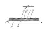
[製造方法]
図4A乃至図4Cは、本実施形態に係る表示装置100の製造方法を説明する断面図である。図4A乃至図4Cを用いて、本実施形態に係る表示装置100の製造方法について詳細に説明する。本実施形態に係る表示装置100の製造方法は、以下の工程を含む。[Production method]
4A to 4C are cross-sectional views illustrating a method of manufacturing the
先ず、第1基板104に複数の画素110が配列されたアレイ基板102を準備する(図4A)。 First, an
第1基板104は、ガラス基板等の支持基板上において、ポリイミド樹脂等をシート状に成形することによって形成された可撓性を有する基板である。そのため、アレイ基板102全体として可撓性を有する。第1基板104上に、複数の画素110を形成する。 The
次いで、複数の画素110を覆う第1絶縁層122及び第2絶縁層124を形成する(図4B)。第1絶縁層122の材料は窒化珪素であり、成膜方法としてはプラズマCVD法又はスパッタリング法を用いることができる。第2絶縁層124はアクリル樹脂であり、成膜方法としては、塗布法又は蒸着法等を用いることができる。 Next, the first insulating
次いで、複数の画素110を覆い、疎密パターン126a、126bを有する第3無機絶縁層を成膜する(図4C)。第3無機絶縁層の成膜装置としては、ロールコータ500を用いることができる。成膜方法としては、例えばプラズマCVD法を用いることができる。 Next, a third inorganic insulating layer having sparse and
図5は、本実施形態に係る表示装置100の製造方法において用いるロールコータ500の構成を説明する概略図である。可撓性を有するアレイ基板102は、成膜室502内において、巻出しロール504から巻付きロール506に搬送される。アレイ基板102は、巻出しロール504と巻付きロール506との間の2つの成膜ロール508を経由する。2つの成膜ロール508の間にプラズマPを発生させ、成膜を行う。これによって、アレイ基板102の搬送とともに、2つの成膜ロール508が最接近する箇所の近傍に成膜材料が堆積される。これによって、アレイ基板102の被成膜面に亘って成膜材料を堆積することができる。 FIG. 5 is a schematic view illustrating the configuration of the
ロールコータ500を用いて本実施形態に係る疎密パターンを有する第3絶縁層126を得るためには、アレイ基板102の搬送速度、所定の疎密パターンが有する縞の間隔によって決定された周期により、成膜条件を動的に変更すればよい。成膜条件とは、例えば、成膜ガス流量、成膜温度、圧力等である。 In order to obtain the third insulating
つまり、アレイ基板102の搬送によって、低密度領域126aに対応する領域が2つの成膜ロール508が最接近する位置の近傍を搬送されている期間と、高密度領域126bに対応する領域が2つの成膜ロール508が最接近する位置の近傍を搬送されている期間とで成膜条件を切り替える。これによって、成膜ロール508の回転軸と同方向の縞状の疎密パターンを有する第3絶縁層126を得ることができる。 That is, there are two regions, one is a period in which the region corresponding to the
次いで、アレイ基板102と対向基板106とを貼り合わせて、図2A及び図2Bに示した本実施形態に係る表示装置100を得ることができる。 Next, the
以上、本実施形態に係る表示装置100の製造方法について説明した。本実施形態に係る表示装置100の製造方法によれば、ロールコータが有する成膜ロール508の回転軸と同方向の縞状の疎密パターンを有する第3絶縁層126を得ることができる。 The manufacturing method of the
<変形例>
本実施形態に係る表示装置100の製造方法の変形例として、プラズマCVD法に替えて、スパッタリング法を用いて第3絶縁層126を形成することができる。<Modification example>
As a modification of the manufacturing method of the
図6は、本実施形態に係る表示装置100の製造方法の変形例において用いるロールコータ600の構成を説明する概略図である。可撓性を有するアレイ基板102は、成膜室602内において、巻出しロール604から巻付きロール606に搬送される。アレイ基板102は、巻出しロール604と巻付きロール606との間の成膜ロール608を経由する。成膜ロール608の一方向には、スパッタリングターゲット610が設置されている。これによって、アレイ基板102の搬送とともに、スパッタリングターゲット610と成膜ロール608とが最接近する箇所の近傍に成膜材料が堆積される。これによって、アレイ基板102の被成膜面に亘って成膜材料を堆積することができる。 FIG. 6 is a schematic view illustrating the configuration of the
ロールコータ600を用いて本実施形態に係る疎密パターンを有する第3絶縁層126を得るためには、アレイ基板102の搬送速度、所定の疎密パターンが有する縞の間隔によって決定された周期により、成膜条件を動的に変更すればよい。成膜条件とは、例えば、成膜ガス流量、成膜温度、圧力等である。 In order to obtain the third insulating
<第2実施形態>
[構成の詳細]
図7は、本実施形態に係る表示装置200の概略構成を説明する断面図である。本実施形態に係る表示装置200は、第1実施形態に係る表示装置100と比べると、封止層120の特に第3絶縁層126の構成のみが異なっている。<Second Embodiment>
[Details of configuration]
FIG. 7 is a cross-sectional view illustrating a schematic configuration of the
封止層120は、第1絶縁層122乃至第3絶縁層126を有し、第3絶縁層126は、複数の絶縁層を含んでいる。第3絶縁層126においては、第1疎密パターンを有する絶縁層及び第2疎密パターンを有する絶縁層が交互に積層されている。 The
第2疎密パターンは、第1疎密パターンを反転したパターンである。つまり、平面構造においては、第2疎密パターンにおける高密度領域126bは、第1疎密パターンにおける低密度領域126aに対応し、第2疎密パターンにおける低密度領域126aは、第1疎密パターンにおける高密度領域126bに対応する。これによって、断面構造においては、隣接する2層の絶縁層において、一方の絶縁層の高密度領域126bは、他方の絶縁層の低密度領域126aに隣接する。 The second sparse and dense pattern is a pattern in which the first sparse and dense pattern is inverted. That is, in the planar structure, the
このような構成を有することによって、アレイ基板102の平面上の任意の箇所の上方には、高密度領域126bが配置された絶縁層が少なくとも1層は存在する。これによって、封止層120に発生し得る水分の経路の内、膜厚方向の経路については、少なくとも1層の高密度領域126bが存在するために遮断される。 By having such a configuration, at least one insulating layer in which the high-
上記の構成に加え、封止層120に発生し得る水分の経路の内、面方向の経路についても遮断される構成とすれば更に好ましい。本実施形態においては、少なくとも最下層の絶縁層の高密度領域126bと、その上層に隣接する絶縁層の高密度領域126bとによって、封止層120の外部から複数の画素110への水分の経路は、膜厚方向及び面方向ともに遮断される。 In addition to the above configuration, it is more preferable to have a configuration in which the path in the plane direction is also blocked among the paths of water that can be generated in the
これによって、封止層120全体としての透湿性が低下する。換言すると、封止層120全体としての防水性が向上する。これによって、信頼性の向上した表示装置200を提供することができる。 As a result, the moisture permeability of the
尚、本実施形態においては、互いに反転の関係にある疎密パターンを積層する態様を示した。しかし、言うまでもなく、上記の作用及び効果を得るには、本実施形態のような封止層120の構成に限られない。 In this embodiment, an embodiment in which sparse and dense patterns having an inversion relationship with each other are laminated is shown. However, needless to say, the above-mentioned actions and effects are not limited to the configuration of the
以上、本実施形態に係る表示装置200の構成について説明した。本実施形態に係る表示装置200の構成によれば、表示装置200の折り曲げへの耐性、及び防水性が向上した表示装置200を提供することができる。 The configuration of the
<第3実施形態>
[構成の詳細]
図8は、本実施形態に係る表示装置300の概略構成を説明する平面図である。本実施形態に係る表示装置300は、第1実施形態に係る表示装置100と比べると、疎密パターンのみが異なっている。つまり、本実施形態に係る表示装置300においては、複数の斑点状の高密度領域126bが、面方向に繰り返し配置されている。つまり、複数の斑点状の高密度領域126bが、面内において、格子状に配置されている。<Third Embodiment>
[Details of configuration]
FIG. 8 is a plan view illustrating a schematic configuration of the display device 300 according to the present embodiment. The display device 300 according to the present embodiment differs from the
また、第1実施形態に係る表示装置100においては、疎密パターンは横方向には有限の繰返し周期を有するが、縦方向には並進対称性を有している。本実施形態に係る表示装置300においては、横方向及び縦方向に有限の繰返し周期を有し、当該周期は両方向で等しい。 Further, in the
このような構成を有することによって、縦方向及び横方向のみならず、他の任意の折り曲げへの耐性が向上する。 By having such a configuration, resistance to not only the vertical direction and the horizontal direction but also any other bending is improved.
尚、本実施形態においては、複数の斑点状の高密度領域126bが、面内において、格子状に配置されている態様について説明した。しかし、これに限られず、種々の変更が可能である。例えば斑点に限らず、他の任意の閉じた曲線であってよい。また、格子状に限らず、互いに角度を有する任意の2方向に対して繰返し周期を有するように配置されていればよい。 In this embodiment, a mode in which a plurality of speckled high-
以上、本実施形態に係る表示装置300の構成について説明した。本実施形態に係る表示装置300の構成によれば、表示装置300の任意の方向の折り曲げへの耐性が向上した表示装置300を提供することができる。 The configuration of the display device 300 according to the present embodiment has been described above. According to the configuration of the display device 300 according to the present embodiment, it is possible to provide the display device 300 having improved resistance to bending of the display device 300 in any direction.
[製造方法]
先ず、図4Aと同様に、第1基板104に複数の画素110が配列されたアレイ基板102を準備する。[Production method]
First, as in FIG. 4A, an
次いで、図4Bと同様に、第1絶縁層122及び第2絶縁層124を形成する。 Next, the first insulating
次いで、アレイ基板102上に第3絶縁層126を形成する。本実施形態においては、基板保持体にアレイ基板102を設置する。疎密パターンを有する第3絶縁層126の成膜においては、基板保持体として、所定のパターンを有する温度勾配を有するものを用いる。 Next, the third insulating
所定のパターンとは、疎密パターンに基づくパターンである。具体的には、基板保持体において、高密度領域126bに対応する領域の温度は、低密度領域126aに対応する領域の温度よりも低くなるように温度勾配を設ける。温度勾配を設けるには、例えば、基板保持体に設置されたヒーターのレイアウトを調整すればよい。成膜方法としては、例えばプラズマCVD法を用いることができる。 The predetermined pattern is a pattern based on a sparse and dense pattern. Specifically, in the substrate holder, a temperature gradient is provided so that the temperature of the region corresponding to the high-
これによって、アレイ基板102の被成膜面が高温であるほど堆積速度が速くなるため、堆積される層の密度が増大し得る。 As a result, the higher the temperature of the surface to be deposited on the
このような温度勾配を設けた状態で、複数の画素110上に、所定のパターンに対応した疎密パターンを有する第3絶縁層126を成膜することができる。 With such a temperature gradient provided, a third
次いで、アレイ基板102と対向基板106とを貼り合わせて、本実施形態に係る表示装置300を得ることができる。 Next, the
以上、本実施形態に係る表示装置300の製造方法について説明した。本実施形態に係る表示装置300の製造方法によれば、任意の疎密パターンを有する第3絶縁層126を得ることができる。 The manufacturing method of the display device 300 according to the present embodiment has been described above. According to the manufacturing method of the display device 300 according to the present embodiment, the third insulating
<第4実施形態>
[構成の詳細]
図9は、本実施形態に係る表示装置400の概略構成を説明する平面図及び断面図である。本実施形態に係る表示装置400は、第2実施形態に係る表示装置200と比べると、疎密パターンのみが異なっている。つまり、本実施形態に係る表示装置400においては、第1疎密パターンは、複数の高密度領域126b及び低密度領域126aが、格子状に繰り返し配置されている。<Fourth Embodiment>
[Details of configuration]
FIG. 9 is a plan view and a cross-sectional view illustrating a schematic configuration of the
このような構成を有することによって、封止層120全体としての透湿性が低下する。換言すると、封止層120全体としての防水性が向上する。更に、縦方向及び横方向のみならず、他の任意の折り曲げへの耐性が向上する。 By having such a configuration, the moisture permeability of the
以上、本実施形態に係る表示装置400の構成について説明した。本実施形態に係る表示装置400の構成によれば、表示装置400の任意の方向の折り曲げへの耐性、及び防水性が向上した表示装置400を提供することができる。 The configuration of the
以上、本発明の好ましい態様を説明した。しかし、これらは単なる例示に過ぎず、本発明の技術的範囲はそれらには限定されない。当業者であれば、本発明の要旨を逸脱することなく、種々の変更が可能であろう。よって、それらの変更も当然に、本発明の技術的範囲に属すると解されるべきである。 The preferred embodiment of the present invention has been described above. However, these are merely examples, and the technical scope of the present invention is not limited thereto. Those skilled in the art will be able to make various changes without departing from the gist of the present invention. Therefore, those changes should, of course, be understood to belong to the technical scope of the present invention.
表示装置・・・100、200、400、400 アレイ基板・・・102 第1基板・・・104 対向基板・・・106 第2基板・・・108 接続端子・・・109 画素・・・110 発光素子・・・112 画素電極・・・114 共通電極・・・116 発光層・・・118 封止層・・・120 第1絶縁層・・・122 第2絶縁層・・・124 第3絶縁層・・・126 低密度領域・・・126a 高密度領域・・・126b バンク・・・128 シール材・・・130 ロールコータ・・・500、600 成膜室・・・502、602 巻出しロール・・・504、604 巻付きロール・・・506、606 成膜ロール・・・508、608 スパッタリングターゲット・・・610 Display device: 100, 200, 400, 400 Array board: 102 First board: 104 Opposing board: 106 Second board: 108 Connection terminal: 109 Pixels: 110 Light emission Element: 112 Pixel electrode: 114 Common electrode: 116 Light emitting layer: 118 Sealing layer: 120 First insulating layer: 122 Second insulating layer: 124 Third insulating layer・ ・ ・ 126 Low density area ・ ・ ・ 126a High density area ・ ・ ・ 126b Bank ・ ・ ・ 128 Sealing material ・ ・ ・ 130 Roll coater ・ ・ ・ 500, 600 Formation chamber ・ ・ ・ 502, 602 Unwinding roll ・ ・ ・504, 604 Winding rolls ... 506, 606 Formation rolls ... 508, 608 Sputtering targets ... 610
Claims (14)
Translated fromJapanese前記複数の画素を覆う封止層とを備え、
前記封止層は、
無機絶縁層であり、凹凸を有する第1の絶縁層と、
有機絶縁層であり、前記第1の絶縁層の上に設けられ、前記第1の絶縁層に接し、前記凹凸を平坦にした平坦面を有する第2の絶縁層と、
無機絶縁層であり、前記第2の絶縁層の平坦面に設けられ、疎密パターンを有する第3の絶縁層と、
を含み、
前記疎密パターンは、低密度領域及び高密度領域を含むパターンであり、
前記低密度領域は、前記第3の絶縁層の前記表示領域内の平均密度よりも前記第3の絶縁層の密度が低い領域であり、
前記高密度領域は、前記第3の絶縁層の前記表示領域内の平均密度よりも前記第3の絶縁層の密度が高い領域であることを特徴とする表示装置。An array substrate that isflexible and has multiple pixels arranged inthe display area,
A sealing layer that covers the plurality of pixels is provided.
The sealing layer is
The first insulating layer, which is an inorganic insulating layer and has irregularities,
A second insulating layer which is an organic insulating layer, is provided on the first insulating layer, is in contact with the first insulating layer, and has a flat surface having flattened irregularities.
An inorganic insulating layer, provided on the flat surface of the second insulating layer,athird insulating layer having a densitypattern,
Including
The sparse and dense pattern is a pattern including a low density region and a high density region.
The low density region is a region in which the density ofthe third insulating layer is lower than the average density ofthe third insulating layer in the display region.
The display device, characterized in that the high-density region is a region in which the density ofthe third insulating layer is higher than the average density ofthe third insulating layer in the display region.
前記第2疎密パターンは、前記第1疎密パターンを反転したパターンであることを特徴とする請求項1に記載の表示装置。In the third insulating layer , an insulating layer having a first sparse and dense pattern and an insulating layer having a second sparse and dense pattern are alternately laminated.
The display device according to claim 1, wherein the second sparse and dense pattern is a pattern obtained by reversing the first sparse and dense pattern.
前記複数の画素を覆う封止層とを備え、
前記封止層は、
無機絶縁層であり、凹凸を有する第1の絶縁層と、
有機絶縁層であり、前記第1の絶縁層の上に設けられ、前記第1の絶縁層に接し、前記凹凸を平坦にした平坦面を有する第2の絶縁層と、
無機絶縁層であり、前記第2の絶縁層の平坦面に設けられ、疎密パターンを有する第3の絶縁層と、
を含む表示装置の製造方法であって、
前記アレイ基板を準備し、
ロールコータを用い、前記第3の絶縁層を成膜することを含み、
前記疎密パターンは、低密度領域及び高密度領域を含むパターンであり、
前記低密度領域は、前記第3の絶縁層の前記表示領域の平均密度よりも前記第3の絶縁層の密度が低い領域であり、
前記高密度領域は、前記第3の絶縁層の前記表示領域の平均密度よりも前記第3の絶縁層の密度が高い領域であることを特徴とする表示装置の製造方法。Anarray substrate that is flexible and has multiple pixels arranged in the display area,
A sealing layer that covers the plurality of pixels is provided.
The sealing layer is
The first insulating layer, which is an inorganic insulating layer and has irregularities,
A second insulating layer which is an organic insulating layer, is provided on the first insulating layer, is in contact with the first insulating layer, and has a flat surface having flattened irregularities.
A third insulating layer which is an inorganic insulating layer and is provided on a flat surface of the second insulating layer and has a sparse and dense pattern.
It is a manufacturing method of a display device including
Preparethe array substrate,
Including formingthe third insulating layer by using a roll coater,
The sparse and dense pattern is a pattern including a low density region and a high density region.
The low-density regions is thethird of thethird region density of the insulating layer is lower than the average density of the display region of the insulating layer,
A method for manufacturing a display device, whereinthe high-density region is a region in which the density ofthe third insulating layer is higher than the average density of the display region ofthe third insulating layer.
前記複数の画素を覆う封止層とを備え、
前記封止層は、
無機絶縁層であり、凹凸を有する第1の絶縁層と、
有機絶縁層であり、前記第1の絶縁層の上に設けられ、前記第1の絶縁層に接し、前記凹凸を平坦にした平坦面を有する第2の絶縁層と、
無機絶縁層であり、前記第2の絶縁層の平坦面に設けられ、疎密パターンを有する第3の絶縁層と、
を含む表示装置の製造方法であって、
前記アレイ基板を準備し、
所定のパターンを有する温度勾配を有する基板保持体に前記アレイ基板を設置し、
前記複数の画素上に、前記所定のパターンに対応した前記疎密パターンを有する第3の絶縁層を成膜することを含み、
前記疎密パターンは、低密度領域及び高密度領域を含むパターンであり、
前記低密度領域は、前記第3の絶縁層の前記表示領域の平均密度よりも前記第3の絶縁層の密度が低い領域であり、
前記高密度領域は、前記第3の絶縁層の前記表示領域の平均密度よりも前記第3の絶縁層の密度が高い領域であることを特徴とする表示装置の製造方法。Anarray substrate that isflexible and has multiple pixels arranged inthe display area,
A sealing layer that covers the plurality of pixels is provided.
The sealing layer is
The first insulating layer, which is an inorganic insulating layer and has irregularities,
A second insulating layer which is an organic insulating layer, is provided on the first insulating layer, is in contact with the first insulating layer, and has a flat surface having flattened irregularities.
A third insulating layer which is an inorganic insulating layer and is provided on a flat surface of the second insulating layer and has a sparse and dense pattern.
It is a manufacturing method of a display device including
Preparethe array substrate,
The array substrate is placed on a substrate holder having a temperature gradient having a predetermined pattern.
On the plurality of pixels, the method comprising depositing athird insulating layer havinga density pattern corresponding to the predetermined pattern,
The sparse and dense pattern is a pattern including a low density region and a high density region.
The low-density regions is thethird of thethird region density of the insulating layer is lower than the average density of the display region of the insulating layer,
A method for manufacturing a display device, whereinthe high-density region is a region in which the density ofthe third insulating layer is higher than the average density of the display region ofthe third insulating layer.
Priority Applications (7)
| Application Number | Priority Date | Filing Date | Title |
|---|---|---|---|
| JP2016144198AJP6783573B2 (en) | 2016-07-22 | 2016-07-22 | Display device |
| US15/608,468US10147905B2 (en) | 2016-07-22 | 2017-05-30 | Display device and method of manufacturing display device |
| US16/178,936US10270060B2 (en) | 2016-07-22 | 2018-11-02 | Display device |
| US16/296,375US10461277B2 (en) | 2016-07-22 | 2019-03-08 | Display device |
| US16/582,283US10741790B2 (en) | 2016-07-22 | 2019-09-25 | Display device |
| US16/920,826US10903450B2 (en) | 2016-07-22 | 2020-07-06 | Display device |
| US17/123,224US11335887B2 (en) | 2016-07-22 | 2020-12-16 | Device |
Applications Claiming Priority (1)
| Application Number | Priority Date | Filing Date | Title |
|---|---|---|---|
| JP2016144198AJP6783573B2 (en) | 2016-07-22 | 2016-07-22 | Display device |
Publications (2)
| Publication Number | Publication Date |
|---|---|
| JP2018014284A JP2018014284A (en) | 2018-01-25 |
| JP6783573B2true JP6783573B2 (en) | 2020-11-11 |
Family
ID=60988151
Family Applications (1)
| Application Number | Title | Priority Date | Filing Date |
|---|---|---|---|
| JP2016144198AActiveJP6783573B2 (en) | 2016-07-22 | 2016-07-22 | Display device |
Country Status (2)
| Country | Link |
|---|---|
| US (6) | US10147905B2 (en) |
| JP (1) | JP6783573B2 (en) |
Families Citing this family (3)
| Publication number | Priority date | Publication date | Assignee | Title |
|---|---|---|---|---|
| JP6783573B2 (en)* | 2016-07-22 | 2020-11-11 | 株式会社ジャパンディスプレイ | Display device |
| CN109671750B (en)* | 2018-12-13 | 2021-04-20 | 云谷(固安)科技有限公司 | Display panel, and preparation method and preparation equipment of display panel |
| JP6814230B2 (en) | 2019-01-11 | 2021-01-13 | 株式会社Joled | Light emitting panel, light emitting device and electronic equipment |
Family Cites Families (29)
| Publication number | Priority date | Publication date | Assignee | Title |
|---|---|---|---|---|
| KR100407413B1 (en)* | 1999-07-19 | 2003-11-28 | 마쯔시다덴기산교 가부시키가이샤 | Reflector, method of fabricating the same, reflective display device comprising reflector, and method of fabricating the same |
| JP5024220B2 (en) | 2008-07-24 | 2012-09-12 | セイコーエプソン株式会社 | ORGANIC ELECTROLUMINESCENT DEVICE, METHOD FOR PRODUCING ORGANIC ELECTROLUMINESCENT DEVICE, ELECTRONIC DEVICE |
| JP2010244697A (en) | 2009-04-01 | 2010-10-28 | Seiko Epson Corp | Organic EL device, method for manufacturing organic EL device, electronic device |
| JP2011204377A (en)* | 2010-03-24 | 2011-10-13 | Sony Corp | Optical function film and method of manufacturing the same, and display device and method of manufacturing the same |
| US8723818B2 (en)* | 2010-09-10 | 2014-05-13 | Atmel Corporation | Touch screen poly layer electrode distribution |
| US11038144B2 (en)* | 2010-12-16 | 2021-06-15 | Samsung Display Co., Ltd. | Organic light-emitting display apparatus |
| US10288254B2 (en)* | 2011-02-25 | 2019-05-14 | 3M Innovative Properties Company | Front-lit reflective display device |
| KR101888222B1 (en)* | 2011-05-13 | 2018-08-13 | 쓰리엠 이노베이티브 프로퍼티즈 컴파니 | Back-lit transmissive display having variable index light extraction layer |
| JP5842008B2 (en)* | 2011-10-24 | 2016-01-13 | パナソニック株式会社 | THIN FILM TRANSISTOR, ORGANIC EL LIGHT EMITTING ELEMENT AND METHOD FOR PRODUCING THIN FILM TRANSISTOR |
| KR20130091206A (en) | 2012-02-07 | 2013-08-16 | 주식회사 엔씰텍 | Apparatus for forming organic material pattern, method for forming organic material pattern, organic light emitting display apparatus and method for organic light emitting display apparatus |
| US9762634B2 (en) | 2012-04-06 | 2017-09-12 | At&T Intellectual Property I, L.P. | System and method to transmit digital broadcast grade video via a cellular data network |
| KR20250009548A (en)* | 2012-05-10 | 2025-01-17 | 가부시키가이샤 한도오따이 에네루기 켄큐쇼 | Semiconductor device |
| TWI492374B (en)* | 2012-12-03 | 2015-07-11 | Au Optronics Corp | Electroluminescent display panel |
| TWI790673B (en)* | 2013-03-07 | 2023-01-21 | 日商半導體能源研究所股份有限公司 | Electronic device |
| US9601718B2 (en)* | 2013-05-24 | 2017-03-21 | Panasonic Corporation | Barrier film, organic el device, flexible substrate, and method for manufacturing barrier film |
| US9293730B2 (en) | 2013-10-15 | 2016-03-22 | Samsung Display Co., Ltd. | Flexible organic light emitting diode display and manufacturing method thereof |
| KR102212764B1 (en) | 2013-10-15 | 2021-02-08 | 삼성디스플레이 주식회사 | Organic light emitting display device and method of manufacturing the same |
| JP2015122248A (en)* | 2013-12-25 | 2015-07-02 | 株式会社ジャパンディスプレイ | Organic EL display device |
| US9818976B2 (en)* | 2014-05-13 | 2017-11-14 | Apple Inc. | Encapsulation layers with improved reliability |
| KR102218649B1 (en)* | 2014-09-16 | 2021-02-23 | 삼성디스플레이 주식회사 | Rollable display device |
| KR102313361B1 (en)* | 2014-11-17 | 2021-10-18 | 삼성디스플레이 주식회사 | Organic light-emitting apparatus, electronic device comprising the same, and the manufacturing method of the organic light-emitting apparatus |
| US9847509B2 (en)* | 2015-01-22 | 2017-12-19 | Industrial Technology Research Institute | Package of flexible environmental sensitive electronic device and sealing member |
| KR102352284B1 (en)* | 2015-02-02 | 2022-01-18 | 삼성디스플레이 주식회사 | Rollable display device |
| KR102427669B1 (en)* | 2015-11-17 | 2022-08-02 | 삼성디스플레이 주식회사 | Flexible display device |
| CN107210384B (en) | 2015-12-31 | 2019-03-15 | 深圳市柔宇科技有限公司 | Encapsulating structure, flexible display screen and encapsulating structure production method |
| JP6692194B2 (en)* | 2016-03-23 | 2020-05-13 | 株式会社ジャパンディスプレイ | Display device |
| US10468434B2 (en)* | 2016-04-08 | 2019-11-05 | Innolux Corporation | Hybrid thin film transistor structure, display device, and method of making the same |
| KR102592564B1 (en)* | 2016-06-13 | 2023-10-23 | 삼성디스플레이 주식회사 | Transistor array panel |
| JP6783573B2 (en)* | 2016-07-22 | 2020-11-11 | 株式会社ジャパンディスプレイ | Display device |
- 2016
- 2016-07-22JPJP2016144198Apatent/JP6783573B2/enactiveActive
- 2017
- 2017-05-30USUS15/608,468patent/US10147905B2/enactiveActive
- 2018
- 2018-11-02USUS16/178,936patent/US10270060B2/enactiveActive
- 2019
- 2019-03-08USUS16/296,375patent/US10461277B2/enactiveActive
- 2019-09-25USUS16/582,283patent/US10741790B2/enactiveActive
- 2020
- 2020-07-06USUS16/920,826patent/US10903450B2/enactiveActive
- 2020-12-16USUS17/123,224patent/US11335887B2/enactiveActive
Also Published As
| Publication number | Publication date |
|---|---|
| US10270060B2 (en) | 2019-04-23 |
| US20200335724A1 (en) | 2020-10-22 |
| US10741790B2 (en) | 2020-08-11 |
| US20200020882A1 (en) | 2020-01-16 |
| JP2018014284A (en) | 2018-01-25 |
| US10461277B2 (en) | 2019-10-29 |
| US10147905B2 (en) | 2018-12-04 |
| US20190074482A1 (en) | 2019-03-07 |
| US20190207158A1 (en) | 2019-07-04 |
| US10903450B2 (en) | 2021-01-26 |
| US20210104703A1 (en) | 2021-04-08 |
| US20180026229A1 (en) | 2018-01-25 |
| US11335887B2 (en) | 2022-05-17 |
Similar Documents
| Publication | Publication Date | Title |
|---|---|---|
| CN106449702B (en) | An organic light-emitting display panel and method of making the same | |
| US9929371B2 (en) | Display device | |
| CN107068715B (en) | Organic light-emitting display panel, organic light-emitting display device and preparation method of organic light-emitting display panel | |
| US6664730B2 (en) | Electrode structure of el device | |
| TWI503043B (en) | Electroluminescent display panel | |
| US10290829B2 (en) | Flexible organic electroluminescent device including sealing layer | |
| JP2018054675A (en) | Display device | |
| US9865843B2 (en) | Display device | |
| JP6640599B2 (en) | Display device | |
| JP6584099B2 (en) | Display device and manufacturing method thereof | |
| US11335887B2 (en) | Device | |
| CN101847652A (en) | Electroluminescent display panel | |
| CN109755410A (en) | Organic light-emitting display panel, preparation method and display device | |
| CN208173590U (en) | OLED flexible display panels and electronic equipment | |
| CN109671751B (en) | Display device, display panel and manufacturing method thereof | |
| JP2016201257A (en) | Method of manufacturing display device | |
| KR100775827B1 (en) | Organic EL device including scan line with uniform resistance | |
| JP2007073345A (en) | Display device | |
| US20180090708A1 (en) | Display device | |
| CN115411077A (en) | Display panels and electronic equipment | |
| JP2018156722A (en) | Organic EL panel | |
| JPWO2014162934A1 (en) | Optical device | |
| JP2015122270A (en) | Light emitting device | |
| WO2013186918A1 (en) | Organic electroluminescence device |
Legal Events
| Date | Code | Title | Description |
|---|---|---|---|
| A621 | Written request for application examination | Free format text:JAPANESE INTERMEDIATE CODE: A621 Effective date:20190325 | |
| A977 | Report on retrieval | Free format text:JAPANESE INTERMEDIATE CODE: A971007 Effective date:20200207 | |
| A131 | Notification of reasons for refusal | Free format text:JAPANESE INTERMEDIATE CODE: A131 Effective date:20200218 | |
| A521 | Request for written amendment filed | Free format text:JAPANESE INTERMEDIATE CODE: A523 Effective date:20200415 | |
| TRDD | Decision of grant or rejection written | ||
| A01 | Written decision to grant a patent or to grant a registration (utility model) | Free format text:JAPANESE INTERMEDIATE CODE: A01 Effective date:20201006 | |
| A61 | First payment of annual fees (during grant procedure) | Free format text:JAPANESE INTERMEDIATE CODE: A61 Effective date:20201022 | |
| R150 | Certificate of patent or registration of utility model | Ref document number:6783573 Country of ref document:JP Free format text:JAPANESE INTERMEDIATE CODE: R150 | |
| R250 | Receipt of annual fees | Free format text:JAPANESE INTERMEDIATE CODE: R250 | |
| R250 | Receipt of annual fees | Free format text:JAPANESE INTERMEDIATE CODE: R250 | |
| S111 | Request for change of ownership or part of ownership | Free format text:JAPANESE INTERMEDIATE CODE: R313113 | |
| R350 | Written notification of registration of transfer | Free format text:JAPANESE INTERMEDIATE CODE: R350 |