JP6783537B2 - Manufacturing method of the connector - Google Patents
Manufacturing method of the connectorDownload PDFInfo
- Publication number
- JP6783537B2 JP6783537B2JP2016060736AJP2016060736AJP6783537B2JP 6783537 B2JP6783537 B2JP 6783537B2JP 2016060736 AJP2016060736 AJP 2016060736AJP 2016060736 AJP2016060736 AJP 2016060736AJP 6783537 B2JP6783537 B2JP 6783537B2
- Authority
- JP
- Japan
- Prior art keywords
- electronic component
- anisotropic conductive
- conductive film
- manufacturing
- connector according
- Prior art date
- Legal status (The legal status is an assumption and is not a legal conclusion. Google has not performed a legal analysis and makes no representation as to the accuracy of the status listed.)
- Active
Links
Images


Classifications
- H—ELECTRICITY
- H01—ELECTRIC ELEMENTS
- H01L—SEMICONDUCTOR DEVICES NOT COVERED BY CLASS H10
- H01L24/00—Arrangements for connecting or disconnecting semiconductor or solid-state bodies; Methods or apparatus related thereto
- H01L24/80—Methods for connecting semiconductor or other solid state bodies using means for bonding being attached to, or being formed on, the surface to be connected
- H01L24/83—Methods for connecting semiconductor or other solid state bodies using means for bonding being attached to, or being formed on, the surface to be connected using a layer connector
- H—ELECTRICITY
- H05—ELECTRIC TECHNIQUES NOT OTHERWISE PROVIDED FOR
- H05K—PRINTED CIRCUITS; CASINGS OR CONSTRUCTIONAL DETAILS OF ELECTRIC APPARATUS; MANUFACTURE OF ASSEMBLAGES OF ELECTRICAL COMPONENTS
- H05K3/00—Apparatus or processes for manufacturing printed circuits
- H05K3/30—Assembling printed circuits with electric components, e.g. with resistor
- H05K3/32—Assembling printed circuits with electric components, e.g. with resistor electrically connecting electric components or wires to printed circuits
- H05K3/321—Assembling printed circuits with electric components, e.g. with resistor electrically connecting electric components or wires to printed circuits by conductive adhesives
- H05K3/323—Assembling printed circuits with electric components, e.g. with resistor electrically connecting electric components or wires to printed circuits by conductive adhesives by applying an anisotropic conductive adhesive layer over an array of pads
- H—ELECTRICITY
- H01—ELECTRIC ELEMENTS
- H01B—CABLES; CONDUCTORS; INSULATORS; SELECTION OF MATERIALS FOR THEIR CONDUCTIVE, INSULATING OR DIELECTRIC PROPERTIES
- H01B13/00—Apparatus or processes specially adapted for manufacturing conductors or cables
- H01B13/0026—Apparatus for manufacturing conducting or semi-conducting layers, e.g. deposition of metal
- H—ELECTRICITY
- H01—ELECTRIC ELEMENTS
- H01L—SEMICONDUCTOR DEVICES NOT COVERED BY CLASS H10
- H01L2224/00—Indexing scheme for arrangements for connecting or disconnecting semiconductor or solid-state bodies and methods related thereto as covered by H01L24/00
- H01L2224/73—Means for bonding being of different types provided for in two or more of groups H01L2224/10, H01L2224/18, H01L2224/26, H01L2224/34, H01L2224/42, H01L2224/50, H01L2224/63, H01L2224/71
- H01L2224/732—Location after the connecting process
- H01L2224/73201—Location after the connecting process on the same surface
- H01L2224/73203—Bump and layer connectors
- H01L2224/73204—Bump and layer connectors the bump connector being embedded into the layer connector
- H—ELECTRICITY
- H01—ELECTRIC ELEMENTS
- H01L—SEMICONDUCTOR DEVICES NOT COVERED BY CLASS H10
- H01L2224/00—Indexing scheme for arrangements for connecting or disconnecting semiconductor or solid-state bodies and methods related thereto as covered by H01L24/00
- H01L2224/80—Methods for connecting semiconductor or other solid state bodies using means for bonding being attached to, or being formed on, the surface to be connected
- H01L2224/83—Methods for connecting semiconductor or other solid state bodies using means for bonding being attached to, or being formed on, the surface to be connected using a layer connector
- H01L2224/83009—Pre-treatment of the layer connector or the bonding area
- H01L2224/83048—Thermal treatments, e.g. annealing, controlled pre-heating or pre-cooling
- H—ELECTRICITY
- H01—ELECTRIC ELEMENTS
- H01L—SEMICONDUCTOR DEVICES NOT COVERED BY CLASS H10
- H01L2224/00—Indexing scheme for arrangements for connecting or disconnecting semiconductor or solid-state bodies and methods related thereto as covered by H01L24/00
- H01L2224/80—Methods for connecting semiconductor or other solid state bodies using means for bonding being attached to, or being formed on, the surface to be connected
- H01L2224/83—Methods for connecting semiconductor or other solid state bodies using means for bonding being attached to, or being formed on, the surface to be connected using a layer connector
- H01L2224/8312—Aligning
- H01L2224/83143—Passive alignment, i.e. self alignment, e.g. using surface energy, chemical reactions, thermal equilibrium
- H—ELECTRICITY
- H01—ELECTRIC ELEMENTS
- H01L—SEMICONDUCTOR DEVICES NOT COVERED BY CLASS H10
- H01L2224/00—Indexing scheme for arrangements for connecting or disconnecting semiconductor or solid-state bodies and methods related thereto as covered by H01L24/00
- H01L2224/80—Methods for connecting semiconductor or other solid state bodies using means for bonding being attached to, or being formed on, the surface to be connected
- H01L2224/83—Methods for connecting semiconductor or other solid state bodies using means for bonding being attached to, or being formed on, the surface to be connected using a layer connector
- H01L2224/832—Applying energy for connecting
- H01L2224/83201—Compression bonding
- H01L2224/83203—Thermocompression bonding, e.g. diffusion bonding, pressure joining, thermocompression welding or solid-state welding
- H—ELECTRICITY
- H05—ELECTRIC TECHNIQUES NOT OTHERWISE PROVIDED FOR
- H05K—PRINTED CIRCUITS; CASINGS OR CONSTRUCTIONAL DETAILS OF ELECTRIC APPARATUS; MANUFACTURE OF ASSEMBLAGES OF ELECTRICAL COMPONENTS
- H05K2201/00—Indexing scheme relating to printed circuits covered by H05K1/00
- H05K2201/01—Dielectrics
- H05K2201/0104—Properties and characteristics in general
- H05K2201/0108—Transparent
Landscapes
- Engineering & Computer Science (AREA)
- Manufacturing & Machinery (AREA)
- Microelectronics & Electronic Packaging (AREA)
- Computer Hardware Design (AREA)
- Power Engineering (AREA)
- Electric Connection Of Electric Components To Printed Circuits (AREA)
- Wire Bonding (AREA)
- Manufacturing Of Electrical Connectors (AREA)
- Combinations Of Printed Boards (AREA)
Description
Translated fromJapanese本発明は、光硬化型の異方性導電フィルムを介して第1の電子部品上に第2の電子部品を接続する接続体の製造方法に関する。 The present invention relates to a method for manufacturing a connector for connecting a second electronic component onto a first electronic component via a photocurable anisotropic conductive film.
従来から、テレビやPCモニタ、携帯電話、携帯型ゲーム機、タブレットPCあるいは車載用モニタ等の各種表示手段として、液晶表示装置が多く用いられている。近年、このような液晶表示装置においては、ファインピッチ化、軽量薄型化等の観点から、液晶駆動用ICを直接液晶表示パネルの基板上に実装するいわゆるCOG(chip on glass)や、液晶駆動回路が形成されたフレキシブル基板を直接液晶表示パネルの基板上に実装するいわゆるFOG(film on glass)が採用されている(例えば特許文献1、2を参照)。 Conventionally, liquid crystal display devices have been widely used as various display means such as televisions, PC monitors, mobile phones, portable game machines, tablet PCs, and in-vehicle monitors. In recent years, in such liquid crystal display devices, so-called COG (chip on glass) in which a liquid crystal driving IC is directly mounted on a substrate of a liquid crystal display panel or a liquid crystal driving circuit is used from the viewpoint of fine pitch, light weight and thinness. A so-called FOG (film on glass) is adopted in which a flexible substrate on which a surface is formed is mounted directly on a substrate of a liquid crystal display panel (see, for example,
例えば熱硬化型の異方性導電フィルムを用いた接続方法は、一般的に熱加圧温度が高く、液晶駆動用IC等の電子部品や透明基板に対する熱衝撃が大きくなる傾向にある。このように透明基板に対する熱衝撃が大きくなると、例えば透明基板の端子部に反りが生じうる。また、異方性導電フィルムが接続された後、常温まで温度が低下する際にも、その温度差に起因してバインダーが収縮し、透明基板の端子部に反りが生じるおそれがある。このように透明基板の端子部に反りが生じる結果、表示ムラや液晶駆動用ICの接続不良が発生するおそれがある。 For example, in the connection method using a thermosetting type anisotropic conductive film, the heat pressurization temperature is generally high, and the thermal impact on electronic components such as liquid crystal driving ICs and transparent substrates tends to be large. When the thermal shock to the transparent substrate becomes large in this way, for example, the terminal portion of the transparent substrate may be warped. Further, even when the temperature drops to room temperature after the anisotropic conductive film is connected, the binder may shrink due to the temperature difference, and the terminal portion of the transparent substrate may warp. As a result of warping of the terminal portion of the transparent substrate in this way, display unevenness and poor connection of the liquid crystal driving IC may occur.
熱硬化型の異方性導電フィルムに代えて、紫外線硬化型の異方性導電フィルムを用いた接続方法も考えられる。紫外線硬化型の異方性導電フィルムを用いた接続方法は、熱硬化型の異方性導電フィルムと比較して、バインダー樹脂を硬化させるために高熱をかける必要がなく、液晶駆動用ICや透明基板に対する熱衝撃による不具合を抑制できる。紫外線硬化型の異方性導電フィルムを用いた低温接続を行うためには、紫外線硬化型の異方性導電フィルムのバインダー樹脂の粘度そのものを下げる必要がある。 A connection method using an ultraviolet curable anisotropic conductive film instead of the thermosetting anisotropic conductive film is also conceivable. Compared with the thermosetting anisotropic conductive film, the connection method using the ultraviolet curable anisotropic conductive film does not require high heat to cure the binder resin, and is transparent to the liquid crystal driving IC. It is possible to suppress defects due to thermal impact on the substrate. In order to perform low temperature connection using an ultraviolet curable anisotropic conductive film, it is necessary to reduce the viscosity itself of the binder resin of the ultraviolet curable anisotropic conductive film.
バインダー樹脂の粘度を下げると、液晶駆動用IC等の電子部品を搭載し、熱圧着手段によって押圧した際や、液晶駆動用ICから熱圧着手段が離間する際に液晶駆動用ICのアライメントずれが発生することが懸念される。このアライメントずれにより、液晶駆動用ICの電極端子と、この電極端子と接続される透明基板の端子部に隣接する端子部とのピッチが狭まってしまい、その結果、導電性粒子を介して短絡する等、接続不良が発生しやすい傾向となる。また、このアライメントずれは電子部品の搭載時にも生じる懸念がある。そのため、接続時にもアライメントずれが発生することは、短絡発生の点からも回避することが求められている。 When the viscosity of the binder resin is lowered, the liquid crystal drive IC is misaligned when an electronic component such as a liquid crystal drive IC is mounted and pressed by a thermocompression bonding means or when the thermocompression bonding means is separated from the liquid crystal drive IC. There is concern that it will occur. Due to this misalignment, the pitch between the electrode terminal of the liquid crystal driving IC and the terminal portion adjacent to the terminal portion of the transparent substrate connected to the electrode terminal is narrowed, and as a result, a short circuit is caused via the conductive particles. Etc., there is a tendency for poor connection to occur. In addition, there is a concern that this misalignment may occur when electronic components are mounted. Therefore, it is required to avoid the occurrence of misalignment even at the time of connection from the viewpoint of short circuit occurrence.
本発明は、上述した課題を解決するものであり、電子部品の接続工程におけるアライメントずれを防止し、接続不良を抑制できる接続体の製造方法を提供することを目的とする。 An object of the present invention is to solve the above-mentioned problems, and to provide a method for manufacturing a connected body capable of preventing an alignment deviation in a connecting process of electronic components and suppressing a connection failure.
上述した課題を解決するために、本発明に係る接続体の製造方法は、第1の電子部品上に、光硬化型の異方性導電フィルムを配置する工程(A)と、異方性導電フィルムを介して、第1の電子部品上に、第2の電子部品を配置する工程(B)と、第2の電子部品側から光照射を行う工程(C)と、加熱ツールで、第2の電子部品側から、第1の電子部品と第2の電子部品とを接続する工程(D)とを有し、工程(D)における第1の電子部品と第2の電子部品とのアライメントズレは、異方性導電フィルムに含有された導電性粒子の粒子径の50%以内である。In order to solve the above-mentioned problems, the method for manufacturing a connector according to the present invention includes a step (A) of arranging a photocurable anisotropic conductive film on a first electronic component and anisotropic conductivity. A step (B) of arranging the second electronic component on the first electronic component via a film, a step (C) of irradiating light from the second electronic component side, and a second heating tool. from the electronic component side,it possesses a step (D) connecting the first electronic component and the second electroniccomponent, misalignment of the first electronic component and the second electronic component in the step (D) Is within 50% of the particle size of the conductive particles contained in the anisotropic conductive film .
本発明によれば、電子部品の接続工程におけるアライメントずれを防止し、接続体の接続不良を抑制することができる。 According to the present invention, it is possible to prevent misalignment in the process of connecting electronic components and suppress poor connection of the connected body.
以下、本発明が適用された接続体の製造方法について、図面を参照しながら詳細に説明する。 Hereinafter, a method for manufacturing a connector to which the present invention is applied will be described in detail with reference to the drawings.
[接続体の製造方法]
本製造方法は、以下の工程(A)、工程(B)、工程(C)、及び工程(D)を有する。
工程(A):第1の電子部品上に、光硬化型の異方性導電フィルムを配置する。
工程(B):異方性導電フィルムを介して、第1の電子部品上に、第2の電子部品を配置する。
工程(C):第2の電子部品側から光照射を行う。
工程(D):加熱ツールで、第2の電子部品側から、第1の電子部品と第2の電子部品とを接続する。[Manufacturing method of connector]
This manufacturing method has the following steps (A), steps (B), steps (C), and steps (D).
Step (A): A photocurable anisotropic conductive film is placed on the first electronic component.
Step (B): The second electronic component is placed on the first electronic component via the anisotropic conductive film.
Step (C): Light irradiation is performed from the second electronic component side.
Step (D): With a heating tool, the first electronic component and the second electronic component are connected from the second electronic component side.
[工程(A)]
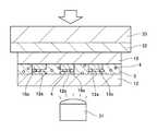
工程(A)では、図1に示すように、第1の電子部品12上に、光硬化型の異方性導電フィルム1を配置(仮貼り)する。第1の電子部品12は、第2の電子部品に接続される電極12aを有する。第1の電子部品12は、例えば、LCDパネルや有機EL(OLED)などのフラットパネルディスプレイ用途、タッチパネル用途などのガラス基板、プリント配線板などが挙げられる。プリント配線板の材質は特に限定されない。プリント配線板の材質は、例えば熱可塑性樹脂などのプラスチックやセラミックなどでもよい。また、ガラス基板も透明性の高いものであれば特に限定されず、熱可塑性樹脂などのプラスチック基板であってもよい。第2の電子部品は特に限定されないが、光照射の光を透過させないものである方が、第2の電子部品の接続前の固定化に適するため好ましい。[Step (A)]
In the step (A), as shown in FIG. 1, a photocurable anisotropic
工程(A)では、例えば図1に示すように、異方性導電フィルム1のバインダー樹脂層3が電極12a側となるように、第1の電子部品12の電極12a上に異方性導電フィルム1を配置する。バインダー樹脂層3を電極12a上に配置した後、剥離フィルム2側からバインダー樹脂層3を例えば熱圧着ツールで加熱及び加圧し、熱圧着ツールを剥離フィルム2から離し、剥離フィルム2をバインダー樹脂層3から剥離する。異方性導電フィルム1の仮貼りは、熱圧着ツールによる加圧及び光照射により行ってもよく、熱加圧と光照射を併用して行ってもよい。 In the step (A), for example, as shown in FIG. 1, the anisotropic conductive film is placed on the
異方性導電フィルム1は、例えば図2に示すように、通常、基材となる剥離フィルム2上に導電性粒子を含有するバインダー樹脂層(接着剤層)3が形成されている。異方性導電フィルムは、ペースト状の異方性導電接着剤と比べて取扱い性に優れる。異方性導電フィルム1は、第1の電子部品12に形成された電極12aと、第2の電子部品18の間にバインダー樹脂層3を介在させることで、第1の電子部品12の電極12aと第2の電子部品18の電極18aとを接続させるために用いられる。異方性導電フィルムの重合型は、カチオン重合型、アニオン重合型、又はラジカル重合型のいずれであってもよい。また、特に支障を来たさなければ、例えばカチオン重合型とラジカル重合型を併用してもよい。また、異方性導電フィルムの重合には、熱と光を併用してもよい。 In the anisotropic
剥離フィルム2としては、異方性導電フィルムにおいて一般に用いられる基材、例えばポリエチレンテレフタレートフィルム等を使用することができる。 As the
バインダー樹脂層3は、バインダー中に導電性粒子4を分散してなるものである。バインダーは、膜形成樹脂、硬化性樹脂、硬化剤、シランカップリング剤等を含有するものであり、通常の異方性導電フィルムに用いられるバインダーを用いることができる。 The
膜形成樹脂としては、例えば平均分子量が10000〜80000程度の樹脂が好ましい。膜形成樹脂としては、フェノキシ樹脂、エポキシ樹脂、変形エポキシ樹脂、ウレタン樹脂等の各種の樹脂が挙げられる。中でも、膜形成状態、接続信頼性等の観点からフェノキシ樹脂が特に好ましい。 As the film-forming resin, for example, a resin having an average molecular weight of about 1000 to 80,000 is preferable. Examples of the film-forming resin include various resins such as phenoxy resin, epoxy resin, deformed epoxy resin, and urethane resin. Of these, phenoxy resin is particularly preferable from the viewpoint of film formation state, connection reliability and the like.
硬化性樹脂としては、特に限定されず、エポキシ樹脂、アクリル樹脂等が挙げられる。エポキシ樹脂としては、特に制限はなく、目的に応じて適宜選択することができる。具体例として、例えば、ナフタレン型エポキシ樹脂、ビフェニル型エポキシ樹脂、フェノールノボラック型エポキシ樹脂、ビスフェノール型エポキシ樹脂、スチルベン型エポキシ樹脂、トリフェノールメタン型エポキシ樹脂、フェノールアラルキル型エポキシ樹脂、ナフトール型エポキシ樹脂、ジシクロペンタジエン型エポキシ樹脂、トリフェニルメタン型エポキシ樹脂等が挙げられる。これらは単独でも、2種以上の組み合わせであってもよい。例えば硬化性樹脂として、エポキシ樹脂とアクリル樹脂とを併用してもよい。 The curable resin is not particularly limited, and examples thereof include an epoxy resin and an acrylic resin. The epoxy resin is not particularly limited and may be appropriately selected depending on the intended purpose. As specific examples, for example, naphthalene type epoxy resin, biphenyl type epoxy resin, phenol novolac type epoxy resin, bisphenol type epoxy resin, stillben type epoxy resin, triphenol methane type epoxy resin, phenol aralkyl type epoxy resin, naphthol type epoxy resin, Examples thereof include a dicyclopentadiene type epoxy resin and a triphenylmethane type epoxy resin. These may be used alone or in combination of two or more. For example, as the curable resin, an epoxy resin and an acrylic resin may be used in combination.
アクリル樹脂としては、特に制限はなく、目的に応じて適宜選択することができ、具体例として、例えば、メチルアクリレート、エチルアクリレート、イソプロピルアクリレート、イソブチルアクリレート、エポキシアクリレート、エチレングリコールジアクリレート、ジエチレングリコールジアクリレート、トリメチロールプロパントリアクリレート、ジメチロールトリシクロデカンジアクリレート、テトラメチレングリコールテトラアクリレート、2−ヒドロキシ−1,3−ジアクリロキシプロパン、2,2−ビス[4−(アクリロキシメトキシ)フェニル]プロパン、2,2−ビス[4−(アクリロキシエトキシ)フェニル]プロパン、ジシクロペンテニルアクリレート、トリシクロデカニルアクリレート、トリス(アクリロキシエチル)イソシアヌレート、ウレタンアクリレート等が挙げられる。これらは単独でも、2種以上の組み合わせであってもよい。 The acrylic resin is not particularly limited and may be appropriately selected depending on the intended purpose. Specific examples thereof include methyl acrylate, ethyl acrylate, isopropyl acrylate, isobutyl acrylate, epoxy acrylate, ethylene glycol diacrylate and diethylene glycol diacrylate. , Trimethylol Propane Triacrylate, Dimethylol Tricyclodecane Diacrylate, Tetramethylene Glycol Tetraacrylate, 2-Hydroxy-1,3-Diacryloxypropane, 2,2-bis [4- (Acryloxymethoxy) Phenyl] Propane , 2,2-Bis [4- (acryloxyethoxy) phenyl] propane, dicyclopentenyl acrylate, tricyclodecanyl acrylate, tris (acryloxyethyl) isocyanurate, urethane acrylate and the like. These may be used alone or in combination of two or more.
硬化剤としては、光硬化型であれば特に制限はなく、目的に応じて適宜選択することができるが、硬化性樹脂がエポキシ樹脂の場合はカチオン系硬化剤が好ましく、アニオン系硬化剤であってもよい。硬化性樹脂がアクリル樹脂の場合はラジカル系硬化剤が好ましい。 The curing agent is not particularly limited as long as it is a photocurable type, and can be appropriately selected depending on the intended purpose. However, when the curable resin is an epoxy resin, a cationic curing agent is preferable, and an anionic curing agent is used. You may. When the curable resin is an acrylic resin, a radical curing agent is preferable.
カチオン系硬化剤としては、特に制限はなく、目的に応じて適宜選択することができ、例えば、スルホニウム塩、オニウム塩等を挙げることができ、これらの中でも、芳香族スルホニウム塩が好ましい。ラジカル系硬化剤としては、特に制限はなく、目的に応じて適宜選択することができ、例えば、有機過酸化物を挙げることができる。 The cationic curing agent is not particularly limited and may be appropriately selected depending on the intended purpose. Examples thereof include sulfonium salts and onium salts. Among these, aromatic sulfonium salts are preferable. The radical-based curing agent is not particularly limited and may be appropriately selected depending on the intended purpose. Examples thereof include organic peroxides.
シランカップリング剤としては、エポキシ系、アミノ系、メルカプト・スルフィド系、ウレイド系等を挙げることができる。シランカップリング剤を添加することにより、有機材料と無機材料との界面における接着性が向上される。 Examples of the silane coupling agent include epoxy-based, amino-based, mercapto-sulfide-based, and ureido-based agents. By adding the silane coupling agent, the adhesiveness at the interface between the organic material and the inorganic material is improved.
導電性粒子4としては、異方性導電フィルムにおいて使用されている公知の何れの導電性粒子を挙げることができる。導電性粒子4としては、例えば、ニッケル、鉄、銅、アルミニウム、錫、鉛、クロム、コバルト、銀、金等の各種金属や金属合金の粒子、金属酸化物、カーボン、グラファイト、ガラス、セラミック、プラスチック等の粒子の表面に金属をコートしたもの、或いは、これらの粒子の表面に更に絶縁薄膜をコートしたもの等が挙げられる。樹脂粒子の表面に金属をコートしたものである場合、樹脂粒子としては、例えば、エポキシ樹脂、フェノール樹脂、アクリル樹脂、アクリロニトリル・スチレン(AS)樹脂、ベンゾグアナミン樹脂、ジビニルベンゼン系樹脂、スチレン系樹脂等の粒子を挙げることができる。導電性粒子は、1種単独で用いてもよいし、2種以上を併用してもよい。 Examples of the
[工程(B)]
工程(B)では、図3に示すように、異方性導電フィルム1を介して、第1の電子部品12上に第2の電子部品18を配置する。第2の電子部品18は、第1の電子部品12と対向する面に電極18aが形成されている。電極18aは、第1の電子部品12の電極12aに対応する間隔で形成されている。電極18aは、例えば金属材料で形成されている。第2の電子部品18としては、例えばフレキシブル基板、テープキャリアパッケージ基板、ICなどが挙げられる。また、ICをフレキシブル基板に実装したCOF(Chip On Film)などであってもよい。[Step (B)]
In the step (B), as shown in FIG. 3, the second
工程(B)では、第2の電子部品18と第1の電子部品12とのアライメントを行うことが好ましい。例えば図3に示すように、各電極12aと各電極18aとがバインダー樹脂層3を介して対向するように、第2の電子部品18を配置する。 In the step (B), it is preferable to align the second
第2の電子部品18上に第1の電子部品12を搭載する際には、一般的に、装置に由来するアライメントズレが発生してしまう傾向にある。従って、接続時に更にアライメントズレが発生することを回避することが望まれる。このような電子部品搭載時のアライメントズレは、例えば第1の電子部品12の電極12a、又は第2の電子部品18の電極18aの短手(幅)に対して5〜10%であることが好ましい。また、工程(D)、すなわち第1の電子部品12と第2の電子部品18とを接続する工程では、さらなるアライメントズレを防止することが求められる。この接続する工程におけるアライメントズレはゼロであることが求められるが、導電性粒子径の50%以内であることが実用上好ましい。接続体としては、電極の短手の10%と導電性粒子径の50%以内のアライメントズレであることが好ましく、電極の短手の5%と導電性粒子径の50%以内のアライメントズレであることがより好ましい。本製造方法では、以下の工程(C)を有することにより、電子部品の接続工程におけるアライメントずれを防止する。 When the first
[工程(C)]
工程(C)では、第2の電子部品18側から光照射を行う。光照射の方法は、例えば図4に示すように、第2の電子部品18側に配置された紫外線照射器31から紫外線を照射する方法が挙げられる。紫外線照射器31としては、LEDランプ、水銀ランプ、メタルハライドランプ等を用いることができる。紫外線が第2の電子部品18及びバインダー樹脂層3に照射されることにより、第2の電子部品18の周縁部のバインダー樹脂層3の硬化が開始されるため、少なくとも第2の電子部品18の周縁部とバインダー樹脂層3とを仮圧着することができる。これにより、例えば後述する工程(D)における第2の電子部品18のアライメントずれを抑制できる。[Step (C)]
In the step (C), light irradiation is performed from the second
工程(C)において照射する積算光量は、第2の電子部品18のアライメントずれを抑制する観点から、例えば200mJ/cm2以上とすることが好ましく、300〜700mJ/cm2とすることがより好ましい。Cumulative amount of light to be irradiated in the step (C) is preferably to be from the viewpoint of suppressing misalignment of the second
[工程(D)]
工程(D)では、加熱ツールで、第2の電子部品18側から、第1の電子部品12と第2の電子部品18とを接続する(本圧着工程)。工程(D)では、例えば図5に示すように、緩衝材32を介して熱圧着ツール30により加熱するとともに、導電性粒子4を第2の電子部品18の電極18a及び電極12aの間で挟持させることが可能となるような圧力で加圧する。熱圧着ツール30による熱加圧温度は、硬化開始前にバインダー樹脂層が溶融したときの粘度(最低溶融粘度)を示す所定の温度に対して±10〜20℃の温度(例えば80℃前後)に設定することが好ましい。これにより、第1の電子部品12の反りを抑制し、熱による第2の電子部品18の損傷を抑制することができる。[Step (D)]
In the step (D), the first
本圧着工程では、第2の電子部品18の電極18aと電極12aとの間からバインダー樹脂が流出するとともに、電極18aと電極12aとの間で導電性粒子4を挟持させる。そして、加熱によりバインダー樹脂が硬化され、図6に示すように、第2の電子部品18が第1の電子部品12上に接続された接続体10が得られる。 In this crimping step, the binder resin flows out from between the
本製造方法では、本圧着工程前に、第2の電子部品18側から光照射を行うことにより、第2の電子部品18の周縁部のバインダー樹脂層3の硬化が開始され、第2の電子部品18の周縁部とバインダー樹脂層3とを仮圧着することができる。また、本圧着工程前に、異方性導電フィルム1のバインダー樹脂の粘度がある程度高められる。そのため、例えば本圧着工程における熱加圧時や熱圧着ツールの離間時に第2の電子部品18のアライメントずれを抑制できる。したがって、アライメントずれによる端子間ショート、例えば電極18aと、電極18aと接続される電極12aに隣接する電極とのピッチが狭まってしまうことにより、導電性粒子4を介して短絡してしまう端子間ショートを抑制できる。特に、ファインピッチ化された電子部品を用いた場合にも同様の効果が得られる。 In this manufacturing method, by irradiating light from the second
なお、本製造方法は、以下に示す工程(E)や、工程(F)をさらに有していてもよい。本製造方法は、例えば工程(A)と工程(B)との間に、図7に示すように、第1の電子部品12上に配置した異方性導電フィルム1全面に対して光(好ましくは紫外線)照射を行う工程(E)をさらに有していてもよい。工程(E)で照射する積算光量は、第2の電子部品18のアライメントずれを抑制する観点、及び工程(D)において接続性を良好にする観点から、大きすぎないことが好ましい。工程(E)における積算光量は、例えば100mJ/cm2未満とすることが好ましく、10〜50mJ/cm2とすることがより好ましい。In addition, this manufacturing method may further include a step (E) and a step (F) shown below. In this manufacturing method, for example, between the step (A) and the step (B), as shown in FIG. 7, light (preferably) is applied to the entire surface of the anisotropic
また、本製造方法は、工程(C)の前後に第2の電子部品18を押圧する工程(F)をさらに有していてもよい。この押圧は、工程(B)において第2の電子部品18を異方性導電フィルム1上に配置する際に行ってもよいし、工程(C)において第2の電子部品18側からの紫外線照射とともに行ってもよい。押圧は、例えば、第2の電子部品18の上面を所定の加熱温度に昇温された熱圧着ツールにより、緩衝材を介して、工程(D)よりも低温、低圧で行うことが好ましい。 Further, the present manufacturing method may further include a step (F) of pressing the second
また、本製造方法は、工程(D)において、例えば図8に示すように、加熱ツールで第1の電子部品12と第2の電子部品18とを接続する際に、光照射を併用してもよい。光照射は、例えば第1の電子部品12側に配置された紫外線照射器31を用いて行うことができる。これにより、バインダー樹脂層3をより効果的に硬化させることができる。工程(D)において光照射を併用する場合、工程(D)における積算光量は、例えば、300〜1200mJ/cm2とすることが好ましい。Further, in the present manufacturing method, in step (D), for example, as shown in FIG. 8, when connecting the first
また、本製造方法は、工程(C)における光照射を工程(A)、すなわち異方性導電フィルム1を配置するときから開始してもよい。 Further, the present manufacturing method may start the light irradiation in the step (C) from the step (A), that is, when the anisotropic
次いで、本技術の実施例について説明する。本実施例では、評価用ICとITOコーティングガラスとを光硬化型の異方性導電フィルムを介して接続した接続体サンプルを得た。そして、得られた接続体サンプルについて、接続初期及び信頼性試験後における導通抵抗値、並びに評価用ICのアライメントずれ量を測定した。なお、本発明は、以下の実施例に限定されるものではない。 Next, examples of the present technology will be described. In this example, a connector sample in which the evaluation IC and the ITO-coated glass were connected via a photocurable anisotropic conductive film was obtained. Then, with respect to the obtained connector sample, the conduction resistance value at the initial stage of connection and after the reliability test, and the amount of misalignment of the evaluation IC were measured. The present invention is not limited to the following examples.
評価素子として、以下の条件の評価用ICを用いた。
外形;1.8mm×20mm
バンプ高さ;15μm
バンプサイズ;30×60μm(最小バンプ間スペース10μm)As the evaluation element, an evaluation IC under the following conditions was used.
External shape: 1.8 mm x 20 mm
Bump height; 15 μm
Bump size: 30 x 60 μm (minimum space between
評価用ICが接続される評価基材として、厚さ0.5mmのITOコーティングガラスを用いた。 An ITO-coated glass having a thickness of 0.5 mm was used as the evaluation base material to which the evaluation IC was connected.
光硬化型の異方性導電フィルムは、以下の方法で得られたものを用いた。下記各成分を酢酸エチル、トルエンにて固形分50%になるように混合溶液を作成し、導電性粒子(AUL704:平均粒子径4μm、積水化学工業株式会社製)を粒子密度が約50,000個/mm2になるように分散させた。
フェノキシ樹脂(YP−50:新日鉄住金化学株式会社製);45質量部
イソシアヌル酸EO変性ジアクリレート(M−215:東亜合成株式会社製);45質量部
シランカップリング剤(KBM−403:信越化学工業株式会社製);2質量部
光ラジカル発生剤(イルガキュア369:BASFジャパン株式会社製);8質量部As the photocurable anisotropic conductive film, the one obtained by the following method was used. A mixed solution was prepared with ethyl acetate and toluene for each of the following components so that the solid content was 50%, and conductive particles (AUL704:
Phenoxy resin (YP-50: manufactured by Nippon Steel & Sumikin Chemical Co., Ltd.); 45 parts by mass of isocyanuric acid EO-modified diacrylate (M-215: manufactured by Toa Synthetic Co., Ltd.); 45 parts by mass of silane coupling agent (KBM-403: Shin-Etsu Chemical Co., Ltd.) (Manufactured by Kogyo Co., Ltd.); 2 parts by mass Photoradical generator (Irgacure 369: manufactured by BASF Japan Co., Ltd.); 8 parts by mass
得られた混合溶液を厚さ50μmのPETフィルム上に塗布し、70℃オーブンにて5分間乾燥し、厚さ20μmのフィルム状に成形した。これにより、光硬化型の異方性導電フィルムを得た。 The obtained mixed solution was applied onto a PET film having a thickness of 50 μm, dried in an oven at 70 ° C. for 5 minutes, and formed into a film having a thickness of 20 μm. As a result, a photocurable anisotropic conductive film was obtained.
[実施例1]
評価基材上に異方性導電フィルムを配置し、この異方性導電フィルムを介して評価基材上に評価用ICを配置した。配置した評価用IC側から、紫外線照射器(ZUV−C30H:オムロン株式会社製)で紫外線を照射し(工程(C))仮圧着を行った。仮圧着後、評価用IC側から熱圧着ツールで熱加圧及び紫外線照射器で紫外線を照射し(工程(D))本圧着を行い、接続体サンプルを得た。[Example 1]
An anisotropic conductive film was placed on the evaluation base material, and an evaluation IC was placed on the evaluation base material via the anisotropic conductive film. Ultraviolet rays were irradiated from the arranged evaluation IC side with an ultraviolet irradiator (ZUV-C30H: manufactured by OMRON Corporation) (step (C)), and temporary crimping was performed. After the temporary crimping, thermocompression bonding was performed from the evaluation IC side with a thermocompression bonding tool and ultraviolet rays were irradiated with an ultraviolet irradiator (step (D)), and the main crimping was performed to obtain a connected sample.
仮圧着時の紫外線照射量は、200mJ/cm2とした。また、本圧着条件は、100℃、80MPa、5秒であり、押圧時には熱圧着ツールと評価用ICの間には緩衝材として厚み50μmのテフロン(登録商標)シートを介した。また、紫外線照射は、熱圧着ツールによる加熱加圧から2秒後に開始し、照射時間は3秒、照度は100mW/cm2とした。本圧着時の紫外線照射は、ガラス基板側から行った。The ultraviolet irradiation amount at the time of temporary crimping was set to 200 mJ / cm2 . The crimping conditions were 100 ° C., 80 MPa, 5 seconds, and a Teflon (registered trademark) sheet having a thickness of 50 μm was used as a cushioning material between the thermocompression bonding tool and the evaluation IC during pressing. The ultraviolet irradiation was started 2 seconds after the heating and pressurization by the thermocompression bonding tool, the irradiation time was 3 seconds, and the illuminance was 100 mW / cm2 . The ultraviolet irradiation during the main crimping was performed from the glass substrate side.
得られた接続体サンプルについて、初期導通抵抗値(Ω)及び信頼性試験後の導通抵抗値(Ω)を測定した。信頼性試験の条件は、温度85℃、相対湿度85%、500時間である。導通抵抗値の測定は、評価用ICのバンプと接続された評価基材の配線にデジタルマルチメータを接続し、4端子法で電流2mAを流したときの抵抗値を測定した。 The initial conduction resistance value (Ω) and the conduction resistance value (Ω) after the reliability test were measured for the obtained connector sample. The conditions of the reliability test are a temperature of 85 ° C., a relative humidity of 85%, and 500 hours. To measure the conduction resistance value, a digital multimeter was connected to the wiring of the evaluation base material connected to the bump of the evaluation IC, and the resistance value when a current of 2 mA was passed by the 4-terminal method was measured.
また、実体顕微鏡を用いて、得られた接続体サンプルのアライメントずれ量(バンプ配列方向、即ちバンプの短手方向)を測定した。なお、評価用IC搭載時のアライメントズレ量は1μm以内であった。接続の前後を確認することで接続時のアライメントズレ量を求めた。接続時のアライメントずれ量の許容範囲は、バンプの短手方向の導電性粒子径の50%以内とした。 In addition, the amount of misalignment (bump arrangement direction, that is, the short side direction of the bump) of the obtained connector sample was measured using a stereomicroscope. The amount of misalignment when the evaluation IC was mounted was within 1 μm. By checking before and after the connection, the amount of misalignment at the time of connection was calculated. The permissible range of the amount of misalignment at the time of connection was set to be within 50% of the diameter of the conductive particles in the lateral direction of the bump.
[実施例2]
仮圧着時の紫外線照射量を600mJ/cm2に変更したこと以外は、実施例1と同様の条件で接続体サンプルを得た。[Example 2]
A connected sample was obtained under the same conditions as in Example 1 except that the ultraviolet irradiation amount at the time of temporary crimping was changed to 600 mJ / cm2 .
[実施例3]
仮圧着時の紫外線照度と照射時間を変更したこと、及び本圧着時に紫外線照射を行わず熱加圧のみを行ったこと以外は、実施例1と同様の条件で接続体サンプルを得た。[Example 3]
A connected sample was obtained under the same conditions as in Example 1 except that the ultraviolet illuminance and irradiation time during temporary crimping were changed, and only thermal pressurization was performed without ultraviolet irradiation during main crimping.
[実施例4]
仮圧着時の紫外線照度と照射時間を変更したこと、及び仮圧着時に評価用IC側から熱圧着ツールで熱加圧を行った後、評価用IC側から紫外線を照射したこと以外は、実施例1と同様の条件で接続体サンプルを得た。仮圧着時の熱加圧条件は、80℃、2MPa、2秒であり、押圧時には熱圧着ツールと評価用ICの間には緩衝材として厚み50μmのテフロン(登録商標)シートを介した。[Example 4]
Examples except that the ultraviolet illuminance and irradiation time at the time of temporary crimping were changed, and that ultraviolet rays were irradiated from the evaluation IC side after performing thermocompression bonding from the evaluation IC side with a thermocompression bonding tool at the time of temporary crimping. A connected sample was obtained under the same conditions as in 1. The thermocompression bonding conditions at the time of temporary crimping were 80 ° C., 2 MPa, and 2 seconds, and at the time of pressing, a Teflon (registered trademark) sheet having a thickness of 50 μm was used as a cushioning material between the thermocompression bonding tool and the evaluation IC.
[実施例5]
仮圧着時の紫外線照度と照射時間を変更したこと、及び仮圧着時に評価用IC側から熱圧着ツールで熱加圧を行った後、評価用IC側から紫外線を照射したこと以外は、実施例3と同様の条件で接続体サンプルを得た。仮圧着時の熱加圧条件は、80℃、2MPa、2秒であり、押圧時には熱圧着ツールと評価用ICの間には緩衝材として厚み50μmのテフロン(登録商標)シートを介した。[Example 5]
Examples except that the ultraviolet illuminance and irradiation time at the time of temporary crimping were changed, and that ultraviolet rays were irradiated from the evaluation IC side after performing thermocompression bonding from the evaluation IC side with a thermocompression bonding tool at the time of temporary crimping. A connector sample was obtained under the same conditions as in 3. The thermocompression bonding conditions at the time of temporary crimping were 80 ° C., 2 MPa, and 2 seconds, and at the time of pressing, a Teflon (registered trademark) sheet having a thickness of 50 μm was used as a cushioning material between the thermocompression bonding tool and the evaluation IC.
[実施例6]
仮圧着時に評価用IC側から紫外線を照射した後に、評価用IC側から熱圧着ツールで熱加圧を行ったこと以外は、実施例1と同様の条件で接続体サンプルを得た。仮圧着時の熱加圧条件は、80℃、2MPa、2秒であり、押圧時には熱圧着ツールと評価用ICの間には緩衝材として厚み50μmのテフロン(登録商標)シートを介した。[Example 6]
A connected sample was obtained under the same conditions as in Example 1 except that after irradiating ultraviolet rays from the evaluation IC side during temporary crimping, heat pressurization was performed from the evaluation IC side with a thermocompression bonding tool. The thermocompression bonding conditions at the time of temporary crimping were 80 ° C., 2 MPa, and 2 seconds, and at the time of pressing, a Teflon (registered trademark) sheet having a thickness of 50 μm was used as a cushioning material between the thermocompression bonding tool and the evaluation IC.
[実施例7]
仮圧着時の紫外線照度と照射時間を変更したこと、及び仮圧着時に評価用IC側から紫外線を照射した後に、評価用IC側から熱圧着ツールで熱加圧を行ったこと以外は、実施例3と同様の条件で接続体サンプルを得た。仮圧着時の熱加圧条件は、80℃、2MPa、2秒であり、押圧時には熱圧着ツールと評価用ICの間には緩衝材として厚み50μmのテフロン(登録商標)シートを介した。[Example 7]
Examples except that the ultraviolet illuminance and irradiation time during temporary crimping were changed, and after irradiating ultraviolet rays from the evaluation IC side during temporary crimping, thermal pressurization was performed from the evaluation IC side with a thermocompression bonding tool. A connected sample was obtained under the same conditions as in 3. The thermocompression bonding conditions at the time of temporary crimping were 80 ° C., 2 MPa, and 2 seconds, and at the time of pressing, a Teflon (registered trademark) sheet having a thickness of 50 μm was used as a cushioning material between the thermocompression bonding tool and the evaluation IC.
[実施例8]
評価基材上に配置した異方性導電フィルム側から、異方性導電フィルム全面に紫外線照射器で紫外線を照射し(工程(E))、紫外線照射後の異方性導電フィルムを介して評価基材上に評価用ICを配置したこと以外は、実施例1と同様の条件で接続体サンプルを得た。[Example 8]
From the anisotropic conductive film side arranged on the evaluation base material, the entire surface of the anisotropic conductive film is irradiated with ultraviolet rays with an ultraviolet irradiator (step (E)), and the evaluation is made through the anisotropic conductive film after the ultraviolet irradiation. A connected sample was obtained under the same conditions as in Example 1 except that the evaluation IC was placed on the base material.
[実施例9]
評価基材上に配置した異方性導電フィルム側から、異方性導電フィルム全面に紫外線照射器で紫外線を照射し、紫外線照射後の異方性導電フィルムを介して評価基材上に評価用ICを配置したこと以外は、実施例3と同様の条件で接続体サンプルを得た。[Example 9]
From the anisotropic conductive film side arranged on the evaluation base material, the entire surface of the anisotropic conductive film is irradiated with ultraviolet rays with an ultraviolet irradiator, and the evaluation base material is evaluated through the anisotropic conductive film after the ultraviolet irradiation. A connected sample was obtained under the same conditions as in Example 3 except that the IC was arranged.
[比較例1]
異方性導電フィルム全面に紫外線を照射する際の積算光量が100mJ/cm2となるように紫外線照射時間を変更したこと以外は、実施例8と同様の条件で行った。[Comparative Example 1]
The same conditions as in Example 8 were carried out except that the ultraviolet irradiation time was changed so that the integrated light amount when irradiating the entire surface of the anisotropic conductive film with ultraviolet rays was 100 mJ / cm2 .
[比較例2]
異方性導電フィルム全面に紫外線を照射する際の積算光量が200mJ/cm2となるように紫外線照射時間を変更したこと以外は、実施例8と同様の条件で行った。[Comparative Example 2]
The same conditions as in Example 8 were carried out except that the ultraviolet irradiation time was changed so that the integrated light amount when irradiating the entire surface of the anisotropic conductive film with ultraviolet rays was 200 mJ / cm2 .

実施例の結果から、電子部品の接続工程におけるアライメントずれを防止することができ、接続体の接続不良を抑制できることが分かった。 From the results of the examples, it was found that the misalignment in the connection process of the electronic components can be prevented and the connection failure of the connected body can be suppressed.
比較例1、2では、得られた接続体サンプルの初期導通抵抗値を測定した際にオーバーレンジが表示された。これは、工程(E)、すなわち異方性導電フィルム全面に紫外線を照射する際の積算光量が大きすぎたため、異方性導電フィルムが本硬化してしまい接続不良が発生したと考えられる。 In Comparative Examples 1 and 2, an overrange was displayed when the initial conduction resistance value of the obtained connector sample was measured. It is considered that this is because the integrated light amount in the step (E), that is, when the entire surface of the anisotropic conductive film is irradiated with ultraviolet rays is too large, the anisotropic conductive film is finally cured and a connection failure occurs.
1 異方性導電フィルム、2 剥離フィルム、3 バインダー樹脂層、4 導電性粒子、10 接続体、12 第1の電子部品、18 第2の電子部品、30 熱圧着ツール、31 紫外線照射器、32 緩衝材1 Anisotropic conductive film, 2 Peeling film, 3 Binder resin layer, 4 Conductive particles, 10 Connectivity, 12 1st electronic component, 18 2nd electronic component, 30 Thermocompression bonding tool, 31 UV irradiator, 32 Cushioning material
Claims (10)
Translated fromJapanese上記異方性導電フィルムを介して、上記第1の電子部品上に、第2の電子部品を配置する工程(B)と、
上記第2の電子部品側から光照射を行う工程(C)と、
加熱ツールで、上記第2の電子部品側から、上記第1の電子部品と上記第2の電子部品とを接続する工程(D)とを有し、
上記工程(D)における上記第1の電子部品と上記第2の電子部品とのアライメントズレ量は、上記異方性導電フィルムに含有された導電性粒子の粒子径の50%以内である、接続体の製造方法。The step (A) of arranging the photocurable anisotropic conductive film on the first electronic component, and
The step (B) of arranging the second electronic component on the first electronic component via the anisotropic conductive film, and
The step (C) of irradiating light from the second electronic component side and
A heating tool, from said second electronic component side,possess a step (D) for connecting the first electronic component and the second electroniccomponent,
The amount of misalignment between the first electronic component and the second electronic component in the step (D) is within 50% of the particle size of the conductive particles contained in the anisotropic conductive film. How to make a body.
Priority Applications (4)
| Application Number | Priority Date | Filing Date | Title |
|---|---|---|---|
| JP2016060736AJP6783537B2 (en) | 2016-03-24 | 2016-03-24 | Manufacturing method of the connector |
| KR1020170017369AKR102665001B1 (en) | 2016-03-24 | 2017-02-08 | Method of manufacturing connector |
| CN201710138673.7ACN107230646B (en) | 2016-03-24 | 2017-03-09 | Method for manufacturing connector |
| HK18104396.2AHK1245501A1 (en) | 2016-03-24 | 2018-04-03 | Method for manufacturing a connector |
Applications Claiming Priority (1)
| Application Number | Priority Date | Filing Date | Title |
|---|---|---|---|
| JP2016060736AJP6783537B2 (en) | 2016-03-24 | 2016-03-24 | Manufacturing method of the connector |
Publications (3)
| Publication Number | Publication Date |
|---|---|
| JP2017175015A JP2017175015A (en) | 2017-09-28 |
| JP2017175015A5 JP2017175015A5 (en) | 2019-04-25 |
| JP6783537B2true JP6783537B2 (en) | 2020-11-11 |
Family
ID=59932480
Family Applications (1)
| Application Number | Title | Priority Date | Filing Date |
|---|---|---|---|
| JP2016060736AActiveJP6783537B2 (en) | 2016-03-24 | 2016-03-24 | Manufacturing method of the connector |
Country Status (4)
| Country | Link |
|---|---|
| JP (1) | JP6783537B2 (en) |
| KR (1) | KR102665001B1 (en) |
| CN (1) | CN107230646B (en) |
| HK (1) | HK1245501A1 (en) |
Families Citing this family (1)
| Publication number | Priority date | Publication date | Assignee | Title |
|---|---|---|---|---|
| CN109637699B (en)* | 2018-12-12 | 2020-05-12 | 武汉华星光电半导体显示技术有限公司 | Method and apparatus for manufacturing anisotropic conductive film |
Family Cites Families (7)
| Publication number | Priority date | Publication date | Assignee | Title |
|---|---|---|---|---|
| CN1314094C (en)* | 2004-02-25 | 2007-05-02 | 友达光电股份有限公司 | Package alignment structure |
| JP4692544B2 (en)* | 2005-04-14 | 2011-06-01 | パナソニック株式会社 | Electronic circuit device and manufacturing method thereof |
| JP5498407B2 (en) | 2011-01-25 | 2014-05-21 | 積水化学工業株式会社 | Method for manufacturing connection structure |
| JP2012175038A (en)* | 2011-02-24 | 2012-09-10 | Sekisui Chem Co Ltd | Method of manufacturing connection structure and anisotropic conductive material |
| JP6133069B2 (en)* | 2013-01-30 | 2017-05-24 | デクセリアルズ株式会社 | Heat curable adhesive film |
| JP5949811B2 (en) | 2014-03-04 | 2016-07-13 | 日立化成株式会社 | Manufacturing method of electronic parts |
| JP6518101B2 (en)* | 2014-03-26 | 2019-05-22 | 積水化学工業株式会社 | PHOTO-CURABLE CONDUCTIVE MATERIAL, CONNECTION STRUCTURE, AND METHOD FOR MANUFACTURING CONNECTION STRUCTURE |
- 2016
- 2016-03-24JPJP2016060736Apatent/JP6783537B2/enactiveActive
- 2017
- 2017-02-08KRKR1020170017369Apatent/KR102665001B1/enactiveActive
- 2017-03-09CNCN201710138673.7Apatent/CN107230646B/enactiveActive
- 2018
- 2018-04-03HKHK18104396.2Apatent/HK1245501A1/enunknown
Also Published As
| Publication number | Publication date |
|---|---|
| JP2017175015A (en) | 2017-09-28 |
| HK1245501A1 (en) | 2018-08-24 |
| CN107230646A (en) | 2017-10-03 |
| CN107230646B (en) | 2023-05-05 |
| KR20170113037A (en) | 2017-10-12 |
| KR102665001B1 (en) | 2024-05-09 |
Similar Documents
| Publication | Publication Date | Title |
|---|---|---|
| JP5972844B2 (en) | Anisotropic conductive film, method for manufacturing anisotropic conductive film, method for manufacturing connected body, and connection method | |
| US10299382B2 (en) | Connection body and connection body manufacturing method | |
| CN105917529B (en) | Connecting body, manufacturing method of connecting body, connecting method, anisotropic conductive adhesive | |
| KR101517323B1 (en) | Connection method, connected-body production method and connected body | |
| WO2013129437A1 (en) | Method for manufacturing connection element, and anisotropic electroconductive adhesive | |
| TW201900812A (en) | Anisotropic conductive adhesive and method of manufacturing the same | |
| JP6679320B2 (en) | Connection body manufacturing method, electronic component connection method | |
| JP5836830B2 (en) | Manufacturing method of connecting body and connecting method | |
| JP5730035B2 (en) | Connection structure manufacturing method, anisotropic conductive connection method, and connection structure | |
| JP6783537B2 (en) | Manufacturing method of the connector | |
| JP6882224B2 (en) | Manufacturing method of connecting body and connecting method of electronic parts | |
| CN104206032B (en) | Manufacturing method of connecting body and connecting method of electronic parts | |
| JP6370562B2 (en) | CONNECTION MANUFACTURING METHOD, FLEXIBLE BOARD CONNECTION METHOD, CONNECTION BODY AND FLEXIBLE SUBSTRATE | |
| JP2017092106A (en) | Anisotropic conductive connection structure and anisotropic conductive connection method | |
| JP6393039B2 (en) | Manufacturing method of connecting body, connecting method and connecting body | |
| WO2015111599A1 (en) | Connection body production method and electronic component connection method | |
| HK1239947A1 (en) | Method for producing connected body, method for connecting electronic component, and connected body | |
| WO2016117613A1 (en) | Method for producing connected body, method for connecting electronic component, and connected body | |
| JP2019140413A (en) | Connection body, manufacturing method of the same, and connection method | |
| JP2015170647A (en) | CONNECTION MANUFACTURING METHOD, ELECTRONIC COMPONENT CONNECTION METHOD, AND CONNECTION BODY |
Legal Events
| Date | Code | Title | Description |
|---|---|---|---|
| A521 | Request for written amendment filed | Free format text:JAPANESE INTERMEDIATE CODE: A523 Effective date:20190313 | |
| A621 | Written request for application examination | Free format text:JAPANESE INTERMEDIATE CODE: A621 Effective date:20190313 | |
| A977 | Report on retrieval | Free format text:JAPANESE INTERMEDIATE CODE: A971007 Effective date:20191220 | |
| A131 | Notification of reasons for refusal | Free format text:JAPANESE INTERMEDIATE CODE: A131 Effective date:20200107 | |
| A521 | Request for written amendment filed | Free format text:JAPANESE INTERMEDIATE CODE: A523 Effective date:20200309 | |
| TRDD | Decision of grant or rejection written | ||
| A01 | Written decision to grant a patent or to grant a registration (utility model) | Free format text:JAPANESE INTERMEDIATE CODE: A01 Effective date:20200923 | |
| A61 | First payment of annual fees (during grant procedure) | Free format text:JAPANESE INTERMEDIATE CODE: A61 Effective date:20201022 | |
| R150 | Certificate of patent or registration of utility model | Ref document number:6783537 Country of ref document:JP Free format text:JAPANESE INTERMEDIATE CODE: R150 | |
| R250 | Receipt of annual fees | Free format text:JAPANESE INTERMEDIATE CODE: R250 | |
| R250 | Receipt of annual fees | Free format text:JAPANESE INTERMEDIATE CODE: R250 | |
| R250 | Receipt of annual fees | Free format text:JAPANESE INTERMEDIATE CODE: R250 |