JP6778553B2 - Atomic layer growth device and atomic layer growth method - Google Patents
Atomic layer growth device and atomic layer growth methodDownload PDFInfo
- Publication number
- JP6778553B2 JP6778553B2JP2016168994AJP2016168994AJP6778553B2JP 6778553 B2JP6778553 B2JP 6778553B2JP 2016168994 AJP2016168994 AJP 2016168994AJP 2016168994 AJP2016168994 AJP 2016168994AJP 6778553 B2JP6778553 B2JP 6778553B2
- Authority
- JP
- Japan
- Prior art keywords
- susceptor
- inert gas
- substrate
- atomic layer
- layer growth
- Prior art date
- Legal status (The legal status is an assumption and is not a legal conclusion. Google has not performed a legal analysis and makes no representation as to the accuracy of the status listed.)
- Active
Links
Images


Classifications
- C—CHEMISTRY; METALLURGY
- C23—COATING METALLIC MATERIAL; COATING MATERIAL WITH METALLIC MATERIAL; CHEMICAL SURFACE TREATMENT; DIFFUSION TREATMENT OF METALLIC MATERIAL; COATING BY VACUUM EVAPORATION, BY SPUTTERING, BY ION IMPLANTATION OR BY CHEMICAL VAPOUR DEPOSITION, IN GENERAL; INHIBITING CORROSION OF METALLIC MATERIAL OR INCRUSTATION IN GENERAL
- C23C—COATING METALLIC MATERIAL; COATING MATERIAL WITH METALLIC MATERIAL; SURFACE TREATMENT OF METALLIC MATERIAL BY DIFFUSION INTO THE SURFACE, BY CHEMICAL CONVERSION OR SUBSTITUTION; COATING BY VACUUM EVAPORATION, BY SPUTTERING, BY ION IMPLANTATION OR BY CHEMICAL VAPOUR DEPOSITION, IN GENERAL
- C23C16/00—Chemical coating by decomposition of gaseous compounds, without leaving reaction products of surface material in the coating, i.e. chemical vapour deposition [CVD] processes
- C23C16/44—Chemical coating by decomposition of gaseous compounds, without leaving reaction products of surface material in the coating, i.e. chemical vapour deposition [CVD] processes characterised by the method of coating
- C23C16/455—Chemical coating by decomposition of gaseous compounds, without leaving reaction products of surface material in the coating, i.e. chemical vapour deposition [CVD] processes characterised by the method of coating characterised by the method used for introducing gases into reaction chamber or for modifying gas flows in reaction chamber
- C23C16/45523—Pulsed gas flow or change of composition over time
- C23C16/45525—Atomic layer deposition [ALD]
- C23C16/45544—Atomic layer deposition [ALD] characterized by the apparatus
- H—ELECTRICITY
- H01—ELECTRIC ELEMENTS
- H01L—SEMICONDUCTOR DEVICES NOT COVERED BY CLASS H10
- H01L21/00—Processes or apparatus adapted for the manufacture or treatment of semiconductor or solid state devices or of parts thereof
- H01L21/67—Apparatus specially adapted for handling semiconductor or electric solid state devices during manufacture or treatment thereof; Apparatus specially adapted for handling wafers during manufacture or treatment of semiconductor or electric solid state devices or components ; Apparatus not specifically provided for elsewhere
- H01L21/683—Apparatus specially adapted for handling semiconductor or electric solid state devices during manufacture or treatment thereof; Apparatus specially adapted for handling wafers during manufacture or treatment of semiconductor or electric solid state devices or components ; Apparatus not specifically provided for elsewhere for supporting or gripping
- H01L21/687—Apparatus specially adapted for handling semiconductor or electric solid state devices during manufacture or treatment thereof; Apparatus specially adapted for handling wafers during manufacture or treatment of semiconductor or electric solid state devices or components ; Apparatus not specifically provided for elsewhere for supporting or gripping using mechanical means, e.g. chucks, clamps or pinches
- H01L21/68714—Apparatus specially adapted for handling semiconductor or electric solid state devices during manufacture or treatment thereof; Apparatus specially adapted for handling wafers during manufacture or treatment of semiconductor or electric solid state devices or components ; Apparatus not specifically provided for elsewhere for supporting or gripping using mechanical means, e.g. chucks, clamps or pinches the wafers being placed on a susceptor, stage or support
- H01L21/68735—Apparatus specially adapted for handling semiconductor or electric solid state devices during manufacture or treatment thereof; Apparatus specially adapted for handling wafers during manufacture or treatment of semiconductor or electric solid state devices or components ; Apparatus not specifically provided for elsewhere for supporting or gripping using mechanical means, e.g. chucks, clamps or pinches the wafers being placed on a susceptor, stage or support characterised by edge profile or support profile
- C—CHEMISTRY; METALLURGY
- C23—COATING METALLIC MATERIAL; COATING MATERIAL WITH METALLIC MATERIAL; CHEMICAL SURFACE TREATMENT; DIFFUSION TREATMENT OF METALLIC MATERIAL; COATING BY VACUUM EVAPORATION, BY SPUTTERING, BY ION IMPLANTATION OR BY CHEMICAL VAPOUR DEPOSITION, IN GENERAL; INHIBITING CORROSION OF METALLIC MATERIAL OR INCRUSTATION IN GENERAL
- C23C—COATING METALLIC MATERIAL; COATING MATERIAL WITH METALLIC MATERIAL; SURFACE TREATMENT OF METALLIC MATERIAL BY DIFFUSION INTO THE SURFACE, BY CHEMICAL CONVERSION OR SUBSTITUTION; COATING BY VACUUM EVAPORATION, BY SPUTTERING, BY ION IMPLANTATION OR BY CHEMICAL VAPOUR DEPOSITION, IN GENERAL
- C23C16/00—Chemical coating by decomposition of gaseous compounds, without leaving reaction products of surface material in the coating, i.e. chemical vapour deposition [CVD] processes
- C23C16/44—Chemical coating by decomposition of gaseous compounds, without leaving reaction products of surface material in the coating, i.e. chemical vapour deposition [CVD] processes characterised by the method of coating
- C23C16/4401—Means for minimising impurities, e.g. dust, moisture or residual gas, in the reaction chamber
- C—CHEMISTRY; METALLURGY
- C23—COATING METALLIC MATERIAL; COATING MATERIAL WITH METALLIC MATERIAL; CHEMICAL SURFACE TREATMENT; DIFFUSION TREATMENT OF METALLIC MATERIAL; COATING BY VACUUM EVAPORATION, BY SPUTTERING, BY ION IMPLANTATION OR BY CHEMICAL VAPOUR DEPOSITION, IN GENERAL; INHIBITING CORROSION OF METALLIC MATERIAL OR INCRUSTATION IN GENERAL
- C23C—COATING METALLIC MATERIAL; COATING MATERIAL WITH METALLIC MATERIAL; SURFACE TREATMENT OF METALLIC MATERIAL BY DIFFUSION INTO THE SURFACE, BY CHEMICAL CONVERSION OR SUBSTITUTION; COATING BY VACUUM EVAPORATION, BY SPUTTERING, BY ION IMPLANTATION OR BY CHEMICAL VAPOUR DEPOSITION, IN GENERAL
- C23C16/00—Chemical coating by decomposition of gaseous compounds, without leaving reaction products of surface material in the coating, i.e. chemical vapour deposition [CVD] processes
- C23C16/44—Chemical coating by decomposition of gaseous compounds, without leaving reaction products of surface material in the coating, i.e. chemical vapour deposition [CVD] processes characterised by the method of coating
- C23C16/455—Chemical coating by decomposition of gaseous compounds, without leaving reaction products of surface material in the coating, i.e. chemical vapour deposition [CVD] processes characterised by the method of coating characterised by the method used for introducing gases into reaction chamber or for modifying gas flows in reaction chamber
- C23C16/45519—Inert gas curtains
- C23C16/45521—Inert gas curtains the gas, other than thermal contact gas, being introduced the rear of the substrate to flow around its periphery
- C—CHEMISTRY; METALLURGY
- C23—COATING METALLIC MATERIAL; COATING MATERIAL WITH METALLIC MATERIAL; CHEMICAL SURFACE TREATMENT; DIFFUSION TREATMENT OF METALLIC MATERIAL; COATING BY VACUUM EVAPORATION, BY SPUTTERING, BY ION IMPLANTATION OR BY CHEMICAL VAPOUR DEPOSITION, IN GENERAL; INHIBITING CORROSION OF METALLIC MATERIAL OR INCRUSTATION IN GENERAL
- C23C—COATING METALLIC MATERIAL; COATING MATERIAL WITH METALLIC MATERIAL; SURFACE TREATMENT OF METALLIC MATERIAL BY DIFFUSION INTO THE SURFACE, BY CHEMICAL CONVERSION OR SUBSTITUTION; COATING BY VACUUM EVAPORATION, BY SPUTTERING, BY ION IMPLANTATION OR BY CHEMICAL VAPOUR DEPOSITION, IN GENERAL
- C23C16/00—Chemical coating by decomposition of gaseous compounds, without leaving reaction products of surface material in the coating, i.e. chemical vapour deposition [CVD] processes
- C23C16/44—Chemical coating by decomposition of gaseous compounds, without leaving reaction products of surface material in the coating, i.e. chemical vapour deposition [CVD] processes characterised by the method of coating
- C23C16/455—Chemical coating by decomposition of gaseous compounds, without leaving reaction products of surface material in the coating, i.e. chemical vapour deposition [CVD] processes characterised by the method of coating characterised by the method used for introducing gases into reaction chamber or for modifying gas flows in reaction chamber
- C23C16/45523—Pulsed gas flow or change of composition over time
- C23C16/45525—Atomic layer deposition [ALD]
- C23C16/45527—Atomic layer deposition [ALD] characterized by the ALD cycle, e.g. different flows or temperatures during half-reactions, unusual pulsing sequence, use of precursor mixtures or auxiliary reactants or activations
- C—CHEMISTRY; METALLURGY
- C23—COATING METALLIC MATERIAL; COATING MATERIAL WITH METALLIC MATERIAL; CHEMICAL SURFACE TREATMENT; DIFFUSION TREATMENT OF METALLIC MATERIAL; COATING BY VACUUM EVAPORATION, BY SPUTTERING, BY ION IMPLANTATION OR BY CHEMICAL VAPOUR DEPOSITION, IN GENERAL; INHIBITING CORROSION OF METALLIC MATERIAL OR INCRUSTATION IN GENERAL
- C23C—COATING METALLIC MATERIAL; COATING MATERIAL WITH METALLIC MATERIAL; SURFACE TREATMENT OF METALLIC MATERIAL BY DIFFUSION INTO THE SURFACE, BY CHEMICAL CONVERSION OR SUBSTITUTION; COATING BY VACUUM EVAPORATION, BY SPUTTERING, BY ION IMPLANTATION OR BY CHEMICAL VAPOUR DEPOSITION, IN GENERAL
- C23C16/00—Chemical coating by decomposition of gaseous compounds, without leaving reaction products of surface material in the coating, i.e. chemical vapour deposition [CVD] processes
- C23C16/44—Chemical coating by decomposition of gaseous compounds, without leaving reaction products of surface material in the coating, i.e. chemical vapour deposition [CVD] processes characterised by the method of coating
- C23C16/458—Chemical coating by decomposition of gaseous compounds, without leaving reaction products of surface material in the coating, i.e. chemical vapour deposition [CVD] processes characterised by the method of coating characterised by the method used for supporting substrates in the reaction chamber
- C23C16/4582—Rigid and flat substrates, e.g. plates or discs
- C23C16/4583—Rigid and flat substrates, e.g. plates or discs the substrate being supported substantially horizontally
- C23C16/4586—Elements in the interior of the support, e.g. electrodes, heating or cooling devices
- H—ELECTRICITY
- H01—ELECTRIC ELEMENTS
- H01L—SEMICONDUCTOR DEVICES NOT COVERED BY CLASS H10
- H01L21/00—Processes or apparatus adapted for the manufacture or treatment of semiconductor or solid state devices or of parts thereof
- H01L21/67—Apparatus specially adapted for handling semiconductor or electric solid state devices during manufacture or treatment thereof; Apparatus specially adapted for handling wafers during manufacture or treatment of semiconductor or electric solid state devices or components ; Apparatus not specifically provided for elsewhere
- H01L21/683—Apparatus specially adapted for handling semiconductor or electric solid state devices during manufacture or treatment thereof; Apparatus specially adapted for handling wafers during manufacture or treatment of semiconductor or electric solid state devices or components ; Apparatus not specifically provided for elsewhere for supporting or gripping
- H01L21/687—Apparatus specially adapted for handling semiconductor or electric solid state devices during manufacture or treatment thereof; Apparatus specially adapted for handling wafers during manufacture or treatment of semiconductor or electric solid state devices or components ; Apparatus not specifically provided for elsewhere for supporting or gripping using mechanical means, e.g. chucks, clamps or pinches
- H01L21/68714—Apparatus specially adapted for handling semiconductor or electric solid state devices during manufacture or treatment thereof; Apparatus specially adapted for handling wafers during manufacture or treatment of semiconductor or electric solid state devices or components ; Apparatus not specifically provided for elsewhere for supporting or gripping using mechanical means, e.g. chucks, clamps or pinches the wafers being placed on a susceptor, stage or support
- H01L21/68785—Apparatus specially adapted for handling semiconductor or electric solid state devices during manufacture or treatment thereof; Apparatus specially adapted for handling wafers during manufacture or treatment of semiconductor or electric solid state devices or components ; Apparatus not specifically provided for elsewhere for supporting or gripping using mechanical means, e.g. chucks, clamps or pinches the wafers being placed on a susceptor, stage or support characterised by the mechanical construction of the susceptor, stage or support
Landscapes
- Chemical & Material Sciences (AREA)
- Engineering & Computer Science (AREA)
- General Chemical & Material Sciences (AREA)
- Chemical Kinetics & Catalysis (AREA)
- Materials Engineering (AREA)
- Mechanical Engineering (AREA)
- Metallurgy (AREA)
- Organic Chemistry (AREA)
- Physics & Mathematics (AREA)
- Condensed Matter Physics & Semiconductors (AREA)
- General Physics & Mathematics (AREA)
- Manufacturing & Machinery (AREA)
- Computer Hardware Design (AREA)
- Microelectronics & Electronic Packaging (AREA)
- Power Engineering (AREA)
- Chemical Vapour Deposition (AREA)
- Container, Conveyance, Adherence, Positioning, Of Wafer (AREA)
Description
Translated fromJapanese本発明は、例えば、基板上に薄膜を形成する原子層成長装置および原子層成長方法に関する。 The present invention relates to, for example, an atomic layer growth apparatus and an atomic layer growth method for forming a thin film on a substrate.
原子層成長技術は、形成される薄膜を構成する元素のガスを基板上に交互に供給し、基板上に原子層単位で薄膜を形成するものであり、薄膜を均一に形成する技術として知られている。また、原子層成長方法は、CVD(Chemical−Vapor−Deposition)法と比較して、段差被覆性や膜厚制御性に優れている。 Atomic layer growth technology is known as a technology for uniformly forming a thin film by alternately supplying gas of elements constituting the thin film to be formed onto a substrate to form a thin film on the substrate in atomic layer units. ing. Further, the atomic layer growth method is superior in step coverage and film thickness controllability as compared with the CVD (Chemical-Vapor-Deposition) method.
原子層成長方法によって薄膜の形成を繰り返し行うと、成膜容器の内壁にも薄膜が付着する。そして、成膜容器の内壁に付着した薄膜の厚さが厚くなると、堆積した薄膜が剥離し、その一部分がパーティクルとなる。したがって、成膜容器の内壁に付着した薄膜を定期的に除去することが必要となる。 When the thin film is repeatedly formed by the atomic layer growth method, the thin film also adheres to the inner wall of the film forming container. Then, when the thickness of the thin film attached to the inner wall of the film forming container becomes thick, the deposited thin film is peeled off and a part thereof becomes particles. Therefore, it is necessary to periodically remove the thin film adhering to the inner wall of the film forming container.
例えば、特開2006−351655号公報(特許文献1)には、防着板を使用し、かつチャンバの内壁に堆積した堆積物を非晶質膜で覆う処理方法および気相成長装置が開示されている。 For example, Japanese Patent Application Laid-Open No. 2006-351655 (Patent Document 1) discloses a treatment method and a vapor phase growth apparatus in which a protective plate is used and the deposits deposited on the inner wall of the chamber are covered with an amorphous film. ing.
また、反応室内に、側壁カバー、床面カバー、上部カバーおよび下部カバーがそれぞれ着脱可能に設けられ、かつサセプタの下面に不活性ガスを流す基板処理装置の構造が、例えば、特開2000−243711号公報(特許文献2)に開示されている。 Further, the structure of the substrate processing apparatus in which the side wall cover, the floor cover, the upper cover and the lower cover are detachably provided in the reaction chamber and the inert gas is flowed to the lower surface of the susceptor is described in, for example, Japanese Patent Application Laid-Open No. 2000-243711. It is disclosed in the publication (Patent Document 2).
また、成膜装置において、基板キャリアに防着部材を取り付けて基板キャリアの表面への膜の付着を防止する旨が、例えば、特開2001−316797号公報(特許文献3)に開示されている。 Further, in the film forming apparatus, for example, Japanese Patent Application Laid-Open No. 2001-316977 (Patent Document 3) discloses that an adhesive member is attached to a substrate carrier to prevent the film from adhering to the surface of the substrate carrier. ..
また、プラズマ処理装置において、処理室内に防着板を設けて基板上以外に絶縁物が付着するのを防ぐ旨が、例えば、特開2014−133927号公報(特許文献4)に開示されている。 Further, in the plasma processing apparatus, for example, Japanese Patent Application Laid-Open No. 2014-133927 (Patent Document 4) discloses that an adhesive plate is provided in the processing chamber to prevent an insulator from adhering to other than on the substrate. ..
原子層成長方法による成膜においては、使用される原料ガス(例えば、TMA:Tri−Methyl−Aluminum)は拡散し易いため、成膜容器内の微細な隙間に容易に侵入して膜を形成する。例えば、成膜室と搬送室とが、ステージストッパーと、ステージもしくはサセプタと、によって区画される原子層成長装置においては、上記区画部分で隙間が生じ、パーティクル発生箇所となり易い。つまり、このような微細な隙間に侵入した原料ガスは、膜及び粉となり、パーティクルの要因となる。 In film formation by the atomic layer growth method, the raw material gas used (for example, TMA: Tri-Methyl-Aluminum) is easily diffused, so that it easily penetrates into minute gaps in the film formation container to form a film. .. For example, in an atomic layer growth apparatus in which a film forming chamber and a transport chamber are partitioned by a stage stopper and a stage or a susceptor, a gap is formed in the compartment and tends to be a particle generation location. That is, the raw material gas that has entered such a fine gap becomes a film and powder, and becomes a factor of particles.
特に、大型のガラス基板に対応した大面積タイプの原子層成長装置においては、基板が大きくなるほどステージも大きくなり、ステージが大きくなるほどステージの平坦度も低下する。その結果、上記区画部分での隙間が増大し、よりパーティクルの発生が顕著となる。 In particular, in a large area type atomic layer growth apparatus corresponding to a large glass substrate, the larger the substrate, the larger the stage, and the larger the stage, the lower the flatness of the stage. As a result, the gap in the compartment is increased, and the generation of particles becomes more remarkable.
その他の課題と新規な特徴は、本明細書の記述および添付図面から明らかになるであろう。 Other challenges and novel features will become apparent from the description and accompanying drawings herein.
一実施の形態による原子層成長装置は、基板に成膜処理が行われる成膜容器と、上記成膜容器内に設置され、上下移動可能なステージと、上記ステージ上に保持され、上記基板を保持するサセプタと、上記ステージの上昇を止め、上記サセプタとの接触により、上記成膜処理が行われる成膜空間と上記基板の搬送が行われる搬送空間とを区画するステージストッパーと、を有する。さらに、上記サセプタは、上記基板を保持する第1サセプタと、上記第1サセプタの周囲に配置された第2サセプタと、を備え、上記第2サセプタ上にサセプタ防着材が設けられている。 The atomic layer growth apparatus according to one embodiment has a film-forming container in which a film-forming process is performed on a substrate, a stage installed in the film-forming container and movable up and down, and a stage held on the stage to hold the substrate. It has a susceptor to be held, and a stage stopper that stops the ascent of the stage and separates the film forming space where the film forming process is performed and the transport space where the substrate is conveyed by contact with the susceptor. Further, the susceptor includes a first susceptor for holding the substrate and a second susceptor arranged around the first susceptor, and a susceptor adhering material is provided on the second susceptor.
また、一実施の形態の原子層成長方法は、(a)ステージ上のサセプタ上に基板を載置する工程、(b)上記(a)工程の後、成膜容器のガス導入部から上記成膜容器内に原料ガスを導入して、上記基板上に上記原料ガスを吸着させる工程、(c)上記(b)工程の後、上記ガス導入部から上記成膜容器内にパージガスを導入して、上記原料ガスを上記成膜容器外に排出する工程、を有する。さらに、(d)上記(c)工程の後、上記ガス導入部から上記成膜容器内に反応ガスを導入して、上記基板上に上記反応ガスを供給し、上記基板の表面に所望の薄膜を形成する工程、(e)上記(d)工程の後、上記ガス導入部から上記成膜容器内にパージガスを導入して、上記反応ガスを上記成膜容器外に排出する工程、を有し、上記(b)〜(e)工程の間、上記成膜容器内に不活性ガスを流す。 Further, the atomic layer growth method of one embodiment consists of (a) a step of placing a substrate on a susceptor on a stage, (b) a step of (a) above, and then a gas introduction portion of a film forming vessel. After the steps of introducing the raw material gas into the membrane container and adsorbing the raw material gas on the substrate, (c) and (b), the purge gas is introduced into the film forming container from the gas introduction section. The step of discharging the raw material gas to the outside of the film forming container. Further, (d) after the step (c), the reaction gas is introduced into the film forming container from the gas introduction section, the reaction gas is supplied onto the substrate, and a desired thin film is formed on the surface of the substrate. (E) After the step (d), there is a step of introducing a purge gas into the film forming container from the gas introducing section and discharging the reaction gas to the outside of the film forming container. During the steps (b) to (e), an inert gas is flowed through the film forming container.
上記一実施の形態によれば、成膜容器内におけるパーティクルの発生を抑制して、基板上に形成される薄膜の膜質を向上させることができる。 According to the above-described embodiment, it is possible to suppress the generation of particles in the film forming container and improve the film quality of the thin film formed on the substrate.
(実施の形態1)
<原子層成長装置の構成>
図1を参照して、本実施の形態の原子層成長装置10の構成を説明する。(Embodiment 1)
<Structure of atomic layer growth device>
The configuration of the atomic
図1は、本実施の形態の原子層成長装置の構造の一例を示す概略構成図である。 FIG. 1 is a schematic configuration diagram showing an example of the structure of the atomic layer growth apparatus of the present embodiment.
本実施の形態1の原子層成長装置10は、基板100に対して原料ガスと反応ガスとを交互に供給し、基板100上に原子層単位で薄膜を形成するものである。その際、反応活性を高めるため、基板100を加熱することができる。本実施の形態1では原料ガスの一例としてTMA(Tri−Methyl−Aluminum)を用い、成膜処理時は、反応活性を高めるため、プラズマを発生させる。本実施の形態1では、プラズマの発生に平行平板電極を用いるが、この方式に限定されるものではない。 The atomic
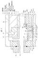
原子層成長装置10に設置された成膜容器(チャンバとも言う)11は、内部で基板100に対して成膜処理を行う容器である。そして、成膜容器11は、インジェクタ21と、排気フランジ31と、平板電極12と、平板電極12の対向電極となるステージ14と、ステージ14上に保持され、かつ基板100を保持する基板保持体であるサセプタ50と、高周波電源16と、を備えている。 The film forming container (also referred to as a chamber) 11 installed in the atomic
平板電極12は、ステージ14と対向して配置されており、成膜空間Sを隔てて基板100の上方に設けられ、平板電極12の側方に配置された絶縁支持体41によって支持されている。絶縁支持体41は、天板42に取り付けられた天板支持部47によって支持されている。そして、絶縁支持体41を保持する天板支持部47の周縁部に、天板支持部47および絶縁支持体41を覆う上部絶縁防着材43を備えている。 The
また、平板電極12のステージ14の方向に露出している面の端部が、平板電極12の端部に相当し、平板電極12の露出している下面側には、導電性の板状の平板電極防着材13が設けられている。 Further, the end portion of the surface of the
ステージ14は、基板100を保持し、かつヒーターを備え、基板100の温度を所望の温度に調整することができる。例えば、原子層成長処理の場合、基板100を50〜200℃に加熱する。成膜容器11は、成膜処理に際し、真空に維持される。そして、高周波電源16が所定の周波数の高周波電流を平板電極12に供給する。 The
なお、ステージ14は上下移動可能な機構を備えており、成膜処理時には、最も上昇した位置で処理が行われる。さらに、ステージ14上には基板100を保持する導電性のサセプタ50が配置されている。したがって、基板100は、サセプタ50上に保持され、高周波電源16が所定の周波数の高周波電流を平板電極12に供給することにより、平板電極12とサセプタ50との間でプラズマが生成される。 The
次に、原料ガス、反応ガス、パージガスが導入されるガス導入部20について説明する。ガス導入部20は、原料ガス、反応ガス、パージガスを、処理過程に従って成膜容器11内に供給するものである。また、インジェクタ21は成膜容器11のガス導入側開口部25に取り付けられており、ガス導入側開口部25に成膜容器11の内側からインジェクタ防着材22が挿入されて、ガス導入側開口部25を囲むように取り付けられる。 Next, the
次に、排気部30について説明する。排気部30は、原料ガス、反応ガス、パージガスを、処理過程に従って成膜容器11から排気するものである。排気フランジ31は成膜容器11のガス排気側開口部33に取り付けられ、ガス排気側開口部33に成膜容器11の内側から排気防着材32が挿入されて、ガス排気側開口部33を囲むように取り付けられる。そして、成膜容器11に導入されたガスは、処理過程に従ってガス導入部20から排気部30に向けて流れる。このガスの流れ方向に沿う方向を以下では側方として説明する。 Next, the
次に、図1〜図3を用いて、サセプタ50およびサセプタ50の周辺の詳細構造について説明する。 Next, the detailed structure of the
図2は図1に示す原子層成長装置における不活性ガス供給路の一例を示す要部拡大断面図、図3は図2に示す不活性ガス供給路の構造の一例を示す部分拡大断面図と拡大平面図である。なお、図2は、図1に示すガス導入部20から排気部30に向けたガス流れ方向に平行なインジェクタ21の保持面から見た場合のサセプタ50の周辺の拡大断面図でもある。 FIG. 2 is an enlarged cross-sectional view of a main part showing an example of the inert gas supply path in the atomic layer growth apparatus shown in FIG. 1, and FIG. 3 is a partially enlarged cross-sectional view showing an example of the structure of the inert gas supply path shown in FIG. It is an enlarged plan view. Note that FIG. 2 is also an enlarged cross-sectional view of the periphery of the
本実施の形態1の原子層成長装置10では、図2に示すように、ステージ14上にサセプタ50が配置されており、基板100はサセプタ50によって保持されている。サセプタ50は、基板100を保持する上部サセプタ52と、上部サセプタ52を支持する下部サセプタ51と、を備えている。さらに、上部サセプタ52は、基板100を保持する保持面52BAを有した上部サセプタ基板保持部(第1サセプタ)52Bと、上部サセプタ基板保持部52Bの周囲に位置し、かつ保持面52BAより低い高さの上部サセプタ周縁部(第2サセプタ)52Aと、を備えている。 In the atomic
また、下部サセプタ51は、ステージ14によって支持され、基板100の保持面52BAよりも高さが低い位置の下部サセプタ周縁部51Aと、上部サセプタ52を保持する下部サセプタ支持部51Bとを有している。なお、ステージストッパー17は、成膜容器11の4つの側壁の内壁11Aに接するように設けられた部材であり、さらに、ステージ14の上昇を止め、かつサセプタ50との接触により、成膜容器11内に、成膜処理が行われる成膜空間Sと、基板100の搬送が行われる図1に示す搬送空間Tと、を区画形成するものである。そして、下部サセプタ支持部51B上には導電性の上部サセプタ52が配置されており、基板100を保持する上部サセプタ基板保持部52Bと、その周囲に配置され、かつ上部サセプタ基板保持部52Bよりも低い高さの面を備えた上部サセプタ周縁部52Aとを有している。なお、少なくとも上部サセプタ周縁部52A上にはサセプタ防着材15が設けられ、本実施の形態1の原子層成長装置10では、下部サセプタ周縁部51Aの一部および上部サセプタ周縁部52A上に、サセプタ防着材15が設けられている。 Further, the
また、上部サセプタ周縁部52Aのステージストッパー17側の側面は、ステージストッパー17の基板側の側面より内側に位置しており、上部サセプタ52と下部サセプタ51は、上部サセプタ周縁部52Aにおいて固定ビス54によって固定されている。 Further, the side surface of the upper susceptor
ここで、上部サセプタ周縁部52Aには、不活性ガスを供給する不活性ガス放出部63が取り付けられている。図3に示すように、不活性ガス放出部63は、上部サセプタ基板保持部52Bを囲むように、例えば枠状に形成されており、上方に向けて不活性ガスを供給する複数の不活性ガス供給口63Aが設けられている。そして、不活性ガス供給口63Aは、下部サセプタ支持部51Bの下部不活性ガス供給路62Aに連通している。 Here, an inert
つまり、外部から不活性ガスを供給する不活性ガス供給路Gがサセプタ50に設けられ、上部サセプタ基板保持部52Bと上部サセプタ周縁部52Aとの間の位置に不活性ガス放出部63が配置され、さらにその不活性ガス放出部63に、不活性ガス供給路Gと連通する不活性ガス供給口63Aが形成されている。 That is, an inert gas supply path G for supplying an inert gas from the outside is provided in the
また、図2に示すように、上部サセプタ基板保持部52Bの側面と、サセプタ防着材15の基板側の側面と、の隙間は、上部サセプタ不活性ガス供給路64を構成しており、また、基板100の下面とサセプタ防着材15の上面との隙間は、不活性ガス排出口65を構成している。すなわち、基板100とサセプタ防着材15との隙間からなる不活性ガス排出口65、および上部サセプタ基板保持部52Bとサセプタ防着材15との隙間からなる上部サセプタ不活性ガス供給路64をそれぞれ介して不活性ガスを成膜空間Sに供給する不活性ガス供給路Gがサセプタ50に形成されている。そして、サセプタ50の不活性ガス供給路Gに不活性ガスを供給する不活性ガス供給部61が成膜容器11に設けられている。 Further, as shown in FIG. 2, the gap between the side surface of the upper susceptor
なお、サセプタ50に形成された不活性ガス供給路Gは、上部サセプタ52に形成された上部不活性ガス供給路62Bと、下部サセプタ51に形成された下部不活性ガス供給路62Aと、からなり、上部不活性ガス供給路62Bと、下部不活性ガス供給路62Aと、が連通されている。 The inert gas supply path G formed in the
以上のように本実施の形態1の原子層成長装置10では、外部から不活性ガスを供給し、かつ上部不活性ガス供給路62Bと下部不活性ガス供給路62Aとからなる不活性ガス供給路Gがサセプタ50に形成されている。そして、成膜容器11に、不活性ガス供給路Gと不活性ガス供給チューブ53を介して接続された不活性ガス通気口66が形成されている。 As described above, in the atomic
なお、成膜容器11の内壁11Aに設けられたステージストッパー17の上面には、ステージストッパー防着材24が設けられ、さらに、インジェクタ防着材22の内壁11A側には、側壁防着材26が設けられている。 A stage
ここで、本実施の形態1の課題の詳細について説明する。 Here, the details of the subject of the first embodiment will be described.
原子層成長方法を用いた成膜処理では、それぞれの工程で、ガスの拡散を一旦待って、次の反応剤のガスを導入する。その際、使用される原料ガス(例えば、TMA)が拡散し易いため、成膜容器内の微細な隙間にも原料ガスは容易に侵入して膜を形成する。例えば、成膜容器内に設置されたステージ14およびサセプタ50やその周囲の部材に形成された微細な隙間に対して原料ガスや反応ガスが侵入し、その微細な隙間に着膜が生じる。そして、この着膜がパーティクルの要因となって基板100上に形成される薄膜の特性を劣化させるという課題が生じる。着膜を抑制したい場合には、ガス進入経路となる流路断面積を小さくし、かつ流路距離を大きくし、さらに不活性ガスをパージする必要がある。しかしながら、装置構造上、ガス進入経路となる流路断面積を小さく、かつ流路を大きくできない場合もある。このような場合、着膜を軽減することは可能であるが、着膜を完全に回避することは困難である。 In the film forming process using the atomic layer growth method, the gas of the next reactant is introduced after waiting for the diffusion of the gas in each step. At that time, since the raw material gas used (for example, TMA) is easily diffused, the raw material gas easily penetrates into the minute gaps in the film forming container to form a film. For example, the raw material gas and the reaction gas invade the fine gaps formed in the
なお、成膜装置のうち、例えば、CVD装置では、ドライエッチングによってチャンバ内の余計な膜を除去している。すなわち、チャンバをばらすことなく、クリーニングガス(例えばNF3等)を流してプラズマを形成することで、余計な膜を除去している。Among the film forming apparatus, for example, in the CVD apparatus, an extra film in the chamber is removed by dry etching. That is, the excess film is removed by forming plasma by flowing a cleaning gas (for example, NF3 or the like) without disassembling the chamber.
ところが、原子層成長装置で使用するアルミナ膜(Al2O3)は、ドライエッチングを実施しようとすると高温処理(例えば、800℃)となり、コストがかかる。However, the alumina film (Al2 O3 ) used in the atomic layer growth apparatus is subjected to high temperature treatment (for example, 800 ° C.) when dry etching is to be performed, which is costly.
また、プラズマを利用し、絶縁膜を形成する原子層成長装置においては、膜の堆積により、区画する部分が絶縁化されるため、サセプタ50とステージストッパー17との間で流れる高周波電流の量が成膜を重ねるごとに変化し、成膜再現性が低下するという問題が生じる。また、ステージストッパー17の近傍は、サセプタ50に流れた高周波電流が集中するため、隙間や凹凸が存在すると、その部分でアーキングが生じやすい。これにより、アーキング源となる防着板の継ぎ目やビスを極力低減することが必要となる。 Further, in an atomic layer growth apparatus that uses plasma to form an insulating film, the partitioning portion is insulated by the deposition of the film, so that the amount of high-frequency current flowing between the susceptor 50 and the
また、原子層成長装置が大きくなると、それだけ防着板の枚数が増加するため、メンテナンスの所要時間も増加するという問題も生じる。成膜容器11のメンテナンスは、成膜容器11の天板42を解放し、成膜容器11の上方から成膜空間Sに手を伸ばして作業を行うことになるが、ステージストッパー17の側方面(側面)およびサセプタ近傍は、メンテナンス時の防着板へのアクセスが悪いため、作業性は著しく悪い。 Further, as the atomic layer growth apparatus becomes larger, the number of protective plates increases accordingly, which causes a problem that the time required for maintenance also increases. For maintenance of the
そこで、原子層成長装置において、そのサセプタ50の近傍の防着板には、防着板の表面以外への着膜が抑制され、かつ防着板の着脱が容易である構造が要求される。 Therefore, in the atomic layer growth apparatus, the protective plate in the vicinity of the
本実施の形態1の原子層成長装置10では、ステージストッパー17の内側の領域において、下部サセプタ周縁部51Aおよび上部サセプタ周縁部52A上に、サセプタ防着材15が設けられている。 In the atomic
次に、サセプタ50の周囲の更なる詳細な構造について説明する。 Next, a more detailed structure around the
原子層成長装置10において、上部サセプタ基板保持部52Bの側面と基板100の側面との距離(距離a)は、0.1mm以上、10mm以下が好適である。距離aが大きいことで、原料ガスおよび反応ガスの不活性ガス排出口65の内側への進入が抑制され、上部サセプタ基板保持部52Bへの着膜を軽減することが可能となる。ただし、距離aが大きいと、基板100の外周部が上部サセプタ基板保持部52Bと接触しない領域が増加するため、基板100の外周部で温度低下が生じる。基板100のエッジエクスクルージョンは、5mmであることが一般的であるため、本実施の形態1では、その値となる5mmを好適値とする。 In the atomic
また、上部サセプタ基板保持部52Bの側面とサセプタ防着材15の基板側の側面との隙間(距離b)は、0.1mm以上、10mm以下が好適である。距離bが小さいことで、原料ガスおよび反応ガスの上部サセプタ不活性ガス供給路64の内側への進入が抑制され、上部サセプタ基板保持部52Bおよび上部サセプタ周縁部52Aへの着膜が軽減される。距離bの値が小さすぎる場合、組み立て精度次第では、上部サセプタ基板保持部52Bの側面とサセプタ防着材15とが干渉する。よって、好適値が必要であり、本実施の形態1では0.5mmとする。 Further, the gap (distance b) between the side surface of the upper susceptor
また、基板100とサセプタ防着材15との水平方向の重なり距離(距離c)は、0.1mm以上、10mm以下が好適である。距離cが大きいことで、原料ガスおよび反応ガスの不活性ガス排出口65の内側への進入が抑制される。しかしながら、距離bの値が小さい場合、組み立て精度次第では、上部サセプタ基板保持部52Bの側面とサセプタ防着材15とが干渉する。その際、距離cは、距離a、bの好適値で決まるため、本実施の形態1では距離cを4.5mmとする。 Further, the horizontal overlapping distance (distance c) between the
また、基板100の下面とサセプタ防着材15の上面との隙間(距離d)は、0.1mm以上、10mm以下が好適である。距離dが小さいことで、原料ガスおよび反応ガスの不活性ガス排出口65の内側への進入が抑制される。距離dの値が小さすぎる場合、組み立て精度次第では、基板100とサセプタ防着材15とが干渉する。よって、好適値が必要であり、本実施の形態1では1mmとする。 The gap (distance d) between the lower surface of the
なお、上部サセプタ周縁部52Aは、その内部に、不活性ガス供給口63Aに連通する上部不活性ガス供給路62Bを有しており、上部不活性ガス供給路62Bの終端は、下部サセプタ51に設けられた下部不活性ガス供給路62Aに接続されている。下部不活性ガス供給路62A、上部不活性ガス供給路62Bは、下部サセプタ51および上部サセプタ52に貫通穴を設け、その間に例えばOリングを介することで、不活性ガス供給口63Aに不活性ガスを供給することができる。下部不活性ガス供給路62Aには、下部サセプタ51の外周側に配置した不活性ガス供給チューブ53が接続されており、不活性ガス供給チューブ53の他端側は、成膜容器11に設けた不活性ガス通気口66に接続されている。そして、不活性ガス通気口66には、成膜容器11の外側に設けられた不活性ガス供給部61が接続されている。 The upper
不活性ガス供給チューブ53は、例えば、ステンレス製チューブ、ベローズフレキシブルチューブ等で構成することができる。基板100を成膜容器11内に搬入または搬出する際にはステージ14が上下動するが、不活性ガス供給チューブ53はその上下動に追従することが必要となる。不活性ガス供給チューブ53も不活性ガス供給路の一部を構成するものである。 The inert
図3に示すように、不活性ガスは、不活性ガス放出部63の不活性ガス供給口63Aにより、上部サセプタ不活性ガス供給路64および不活性ガス排出口65の全周からシャワー供給することが好ましい。図3では不活性ガス供給部61を1か所設けているが、数カ所設けることが好ましい。なお、不活性ガス排出口65は、上部サセプタ基板保持部52Bの周囲で全周に沿って複数個、または全周に亘って連続して形成されていてもよい。 As shown in FIG. 3, the inert gas is supplied by the inert
また、各不活性ガス供給口63Aにおけるシャワー穴の径は1〜3mm径の範囲内であることが好ましく、1mm程度でよい。シャワー穴のピッチは10mm〜200mmピッチであることが好ましい。上部サセプタ周縁部52Aに貫通穴を設けてシャワー穴を形成してもよく、シャワープレートを個別に形成し、上部サセプタ周縁部52Aに取り付けてもよい。 Further, the diameter of the shower hole in each of the inert
また、下部サセプタ51と上部サセプタ52との固定は、例えばビスを使用する。ここで、固定ビス54の位置は、上部サセプタ周縁部52A部であることが好ましい。固定ビス54が上部サセプタ基板保持部52Bに存在する場合は、ビス頭が基板100と干渉する可能性がある。また、ビス頭が上部サセプタ基板保持部52Bの上面よりも低い位置に存在する場合は、このビス頭の部分で基板100と接触することができないため、局所的な温度低下が生じる。 Further, for fixing the
また、図2に示すように、本実施の形態1の不活性ガス排出口65においては、その不活性ガス排出口65を構成する、上部サセプタ基板保持部52Bの側面と基板100の側面との距離(距離a)の値を、基板100の温度均一性の劣化を考慮して5mmとしている。さらに、基板100の下面とサセプタ防着材15の上面との隙間(距離d)の値を、基板100とサセプタ防着材15の干渉を考慮して1mmとしている。しかしながら、原料ガスおよび反応ガスの進入を抑制するための流路幅、流路長が十分でない可能性が高い。 Further, as shown in FIG. 2, in the inert
そこで、不活性ガス供給量を増加させることで、不活性ガス排出口65への原料ガスおよび反応ガスの進入を軽減することは可能であるが、流量を増大させると原料ガスおよび反応ガスのガス均一性に影響を与え、膜厚均一性および膜質均一性が劣化する可能性がある。 Therefore, it is possible to reduce the ingress of the raw material gas and the reaction gas into the inert
したがって、上記隙間での粉の発生や上部サセプタ基板保持部52Bへの着膜を完全に抑制するのは困難である可能性が高いため、上部サセプタ52は容易に脱着可能な構造であることが好ましい。 Therefore, it is highly likely that it is difficult to completely suppress the generation of powder in the gap and the film formation on the upper susceptor
そこで、上部サセプタ周縁部52Aの外周部の端面(側面)は、ステージストッパー17の基板側の端面(側面)よりも成膜空間Sの内側に位置していることが好ましい。ステージストッパー17は成膜容器11に完全に固定されているため、その脱着は容易ではないが、上部サセプタ52がステージストッパー17よりも小さなサイズであれば、ステージストッパー17を取り外すことなく、簡単に上方へ取り外すことが可能となり、成膜容器11のメンテナンス性を向上させることができる。 Therefore, it is preferable that the end surface (side surface) of the outer peripheral portion of the upper susceptor
なお、不活性ガスは、ステージ14の面温度と±10%以内の温度まで加熱された後に不活性ガス供給口63Aから放出され、さらに不活性ガス排出口65を介して排出されることが好ましい。例えば、ステージを100℃に加熱する場合、常温の不活性ガスを供給すると、下部サセプタ51および上部サセプタ52の外周が冷却されるため、基板100の温度分布も低下し、膜厚均一性および膜質均一性が低下する。したがって、下部サセプタ51および上部サセプタ52の温度を一定に保つため、例えば90〜110℃の不活性ガスを供給することが好ましい。 It is preferable that the inert gas is heated to the surface temperature of the
本実施の形態1の原子層成長装置10によれば、ステージ14上に配置されるサセプタ50上にサセプタ防着材15が設けられたことにより、サセプタ50への着膜を抑制することができる。 According to the atomic
具体的には、基板100を保持する上部サセプタ52における上部サセプタ周縁部52Aの上面と、下部サセプタ51の下部サセプタ周縁部51Aの上面とに、サセプタ防着材15が設けられたことにより、上部サセプタ周縁部52Aや下部サセプタ周縁部51Aへの着膜、および上部サセプタ周縁部52Aと下部サセプタ周縁部51Aとの隙間への着膜を抑制することができる。 Specifically, the upper surface of the upper susceptor
特に、原子層成長装置10で使用されるTMA等の原料ガスは、拡散性が強いため、成膜容器11内の種々の隙間に侵入し易いが、サセプタ50がサセプタ防着材15で覆われていることにより、サセプタ50やサセプタ50周辺の隙間への原料ガスの侵入を防ぐことができる。その結果、薄膜や粉等からなるパーティクルの発生を抑制することができる。 In particular, the raw material gas such as TMA used in the atomic
これにより、成膜容器11内におけるパーティクルの発生を抑制して、基板100上に形成される薄膜の膜質を向上させることができる。 As a result, it is possible to suppress the generation of particles in the
また、上部サセプタ52における上部サセプタ周縁部52Aの側面の位置が、ステージストッパー17の基板側の側面の位置より内側に配置されていることにより、上部サセプタ52を容易に着脱することができる。その結果、成膜容器11および上部サセプタ52のメンテナンス作業性を向上させることができる。 Further, since the position of the side surface of the upper susceptor
また、サセプタ50に、下部不活性ガス供給路62Aと上部不活性ガス供給路62Bとからなる不活性ガス供給路Gが形成されていることにより、成膜処理時に、サセプタ防着材15と上部サセプタ基板保持部52Bとの間の隙間、および基板100とサセプタ防着材15との隙間に、それぞれ不活性ガスを流すことができる。 Further, since the inert gas supply path G including the lower inert
これにより、サセプタ防着材15の側面付近への原料ガスの侵入を阻止することができ、サセプタ50への着膜を抑制することができる。その結果、成膜容器11のメンテナンスの頻度を低減して原子層成長装置10の稼働率を向上させることができる。 As a result, it is possible to prevent the raw material gas from entering the vicinity of the side surface of the susceptor
また、サセプタ50に不活性ガス供給路Gが形成されていることにより、ステージ14に不活性ガス供給路を形成する場合と比較して、コストの低減化を図ることができる。さらに、不活性ガス供給路をステージ14に形成する場合には、ステージ14の設計が困難であることに対して、不活性ガス供給路をサセプタ50に形成する方が、ステージ14の設計が容易である。また、サセプタ50に不活性ガス供給路を形成する方が、ステージ14に形成するのに比べて、より自由度を高めることができる。 Further, since the inert gas supply path G is formed in the
<原子層成長方法>
次に、原子層成長装置10を用いた薄膜形成の処理手順(原子層成長方法)を説明する。<Atomic layer growth method>
Next, a thin film formation processing procedure (atomic layer growth method) using the atomic
図4は実施の形態の原子層成長方法の一例を示すフロー図、図5(a)〜(d)は図4に示すフローに沿った薄膜形成の手順の一例を示す基板断面図である。 FIG. 4 is a flow chart showing an example of the atomic layer growth method of the embodiment, and FIGS. 5 (a) to 5 (d) are cross-sectional views of a substrate showing an example of a procedure for forming a thin film along the flow shown in FIG.
まず、図1に示す成膜容器11内に設けられたステージ14上に基板100を載置する。 First, the
次に、原料ガス供給部が成膜容器11の内部に原料ガスを供給する(図4に示すステップs1)。具体的には、図1に示す成膜容器11のガス導入部20に原料ガスを供給する(ステップs1)。原料ガスは、例えば、TMAであり、成膜容器11の内部に供給される。原料ガスは、例えば、0.1秒間、成膜容器11の内部に供給する。図5(a)に示されるように、ステップs1によって、成膜容器11の内部に原料ガス110が供給され、基板100の上に原料ガス110が吸着して、吸着層102が形成される。 Next, the raw material gas supply unit supplies the raw material gas to the inside of the film forming container 11 (step s1 shown in FIG. 4). Specifically, the raw material gas is supplied to the
また、ステップs1において、図2に示す不活性ガス供給部61からも窒素等の不活性ガスFを図1に示す成膜容器11の内部に供給する。具体的には、サセプタ50に形成された不活性ガス供給路Gを介して成膜空間Sに不活性ガスを供給する。本実施の形態1では、ステップs1のみでなく、後述するステップs2〜s4も含めて、常に成膜容器11内に不活性ガスFを供給する。これにより、基板100とサセプタ防着材15の隙間、および上部サセプタ基板保持部52Bとサセプタ防着材15との隙間に、それぞれ原料ガスおよび反応ガスが入り込むのを軽減することが可能となり、上記各隙間への着膜の抑制化を図ることができる。 Further, in step s1, the inert gas F such as nitrogen is also supplied from the inert
次に、原料ガス110の供給を停止し、ガス導入部20からパージガスを供給する(図4に示すステップs2)。パージガスは、成膜容器11の内部に供給される。原料ガス110は、成膜容器11の排気部30から成膜容器11の外部に排出される。 Next, the supply of the
上記パージガスは、例えば、0.1秒間、成膜容器11の内部に供給する。そして、排気部30が成膜容器11の内部の原料ガス110やパージガス112を排気する。排気部30は、例えば、2秒間、成膜容器11の内部の原料ガス110やパージガス112を排気する。図5(b)に示されるように、ステップs2によって、成膜容器11の内部にパージガス112が供給され、基板100の上に吸着していない原料ガス110が成膜容器11からパージされる。その際、不活性ガスFも不活性ガス供給部61から供給する。 The purge gas is supplied to the inside of the
次に、成膜容器11の内部に反応ガスを供給する(図4に示すステップs3)。具体的には、ガス導入部20を通して反応ガスを供給する(ステップs3)。反応ガスは、ガス導入部20の通路を通って、成膜容器11の内部に供給される。反応ガスは、例えば、1秒間、成膜容器11の内部に供給される。図5(c)に示されるように、ステップs3によって、成膜容器11の内部に反応ガス114が供給され、基板100の表面に所望の薄膜層104が形成される。なお、薄膜層104は、一例として、有機ELの保護膜である。また、ステップs3においても不活性ガス供給部61から不活性ガスFを供給する。 Next, the reaction gas is supplied to the inside of the film forming container 11 (step s3 shown in FIG. 4). Specifically, the reaction gas is supplied through the gas introduction unit 20 (step s3). The reaction gas is supplied to the inside of the
次に、反応ガスの供給を停止し、ガス導入部20にパージガスを供給する(図4に示すステップs4)。パージガス112は、成膜容器11の内部に供給される。パージガス112は、排気部30から成膜容器11の外部に排出される。パージガスは、例えば、0.1秒間、成膜容器11の内部に供給される。排気部30が、成膜容器11の内部の反応ガス114やパージガス112を成膜容器11外に排気する。図5(d)に示されるように、ステップs4によって、成膜容器11の内部にパージガス112が供給され、反応ガス114が成膜容器11からパージされる。この時、不活性ガス供給部61から不活性ガスFも供給される。 Next, the supply of the reaction gas is stopped, and the purge gas is supplied to the gas introduction unit 20 (step s4 shown in FIG. 4). The
以上説明したステップs1〜s4により、基板100の上に一原子層分の薄膜層104が形成される。以下、ステップs1〜4を所定回数繰り返すことにより、所望の膜厚の薄膜層104を形成することができる。 By steps s1 to s4 described above, a
以上のように、本実施の形態1の原子層成長装置10では、その成膜処理中(上記ステップs1〜s4の間)、不活性ガス供給部61からサセプタ50に形成された不活性ガス供給路Gを介して成膜容器11内に不活性ガスFが供給される(導入される)。これにより、不活性ガスFが、サセプタ50の側部およびステージ14上の成膜空間Sに供給される。 As described above, in the atomic
詳細には、成膜処理の間、図2に示すように、不活性ガス供給部61から不活性ガスが供給され、基板100とサセプタ防着材15との隙間、および上部サセプタ基板保持部52Bとサセプタ防着材15との隙間のそれぞれに不活性ガスFが流れるため、上部サセプタ基板保持部52Bへの着膜の堆積量を軽減することが可能になる。その結果、成膜容器11内のウェットエッチングによるクリーニング頻度を低減させることができる。 Specifically, during the film forming process, as shown in FIG. 2, the inert gas is supplied from the inert
また、本実施の形態1の原子層成長方法では、成膜処理の間、基板100とサセプタ防着材15との隙間、および上部サセプタ基板保持部52Bとサセプタ防着材15との隙間に、それぞれに不活性ガスFを流し続ける。 Further, in the atomic layer growth method of the first embodiment, during the film forming process, the gap between the
これにより、成膜処理の間、常に成膜容器11内を一定の圧力に維持することができる。成膜容器11内の圧力が変動するとパーティクルが発生し易く、基板100上に形成する薄膜の膜質が悪くなるが、本実施の形態1の原子層成長方法では、成膜処理の間、不活性ガスFを流し続けるため、成膜容器11内の圧力を一定に維持してパーティクルの発生を低減することができる。 As a result, the inside of the
その結果、基板100上に形成される薄膜の膜質を向上させることができる。 As a result, the film quality of the thin film formed on the
また、上記それぞれの隙間に不活性ガスFを流すことにより、上記それぞれの隙間への原料ガス110および反応ガス114の侵入を阻止することができ、ステージストッパー17や各隙間への着膜を抑制することができる。 Further, by flowing the inert gas F through the respective gaps, it is possible to prevent the
ここで、本実施の形態1に示した原子層成長装置10を用いて、370mm×470mmの大面積ガラス基板にAlON薄膜を形成する評価を行ったその結果について説明する。原子層成長装置10における各種値は以下の通りとした。 Here, the result of evaluation of forming an AlON thin film on a large-area glass substrate of 370 mm × 470 mm using the atomic
距離a:5mm、距離b:0.5mm、距離c:4.5mm、距離d:1mm、シャワー穴径:1mm、シャワー穴ピッチ:100mm、ステージ温度:100℃、不活性ガス温度:100℃、不活性ガス流量:500sccmである。 Distance a: 5 mm, Distance b: 0.5 mm, Distance c: 4.5 mm, Distance d: 1 mm, Shower hole diameter: 1 mm, Shower hole pitch: 100 mm, Stage temperature: 100 ° C, Inert gas temperature: 100 ° C, Inert gas flow rate: 500 sccm.
また、液体原料(原料ガス、Al源)としてTMA、反応ガスとして酸素プラズマおよび窒素プラズマを用いた。成膜は図4に示したシーケンスとした。成膜容器11内の圧力は100Paとし、上部不活性ガス供給路62Bおよび下部不活性ガス供給路62Aより不活性ガスFとして窒素1000sccmを供給し、成膜シーケンス中、常時不活性ガスFを供給した。 Further, TMA was used as the liquid raw material (raw material gas, Al source), and oxygen plasma and nitrogen plasma were used as the reaction gas. The film formation was performed in the sequence shown in FIG. The pressure in the
成膜容器11の内部の膜厚が20μmとなるように成膜処理を実施した後、上部サセプタ基板保持部52Bには200nmの着膜が観察されたが、粉の発生は観測されなかった。サセプタ50は、使用する材質と堆積される膜質によるが、本実施の形態1においては、2μmの膜がサセプタ50に堆積された場合にパーティクルを発生することが分かっている。 After the film forming process was performed so that the film thickness inside the
なお、成膜処理中に成膜容器内に不活性ガスを供給しない原子層成長装置では、成膜容器の内部の膜厚が20μmに到達した時点で粉の発生が観察され、その都度ステージストッパーを解体した後、メンテナンスを実施することを必要とした。これに対して、本実施の形態1の原子層成長装置10においては、成膜容器11の内部の膜厚が、上述の不活性ガスを供給しない原子層成長装置と比較して10倍である20μmまでメンテナンスフリーとすることができる。 In the atomic layer growth apparatus that does not supply an inert gas into the film forming container during the film forming process, the generation of powder is observed when the film thickness inside the film forming container reaches 20 μm, and the stage stopper is used each time. It was necessary to carry out maintenance after dismantling. On the other hand, in the atomic
さらに、メンテナンス時は、上部サセプタ52の脱着を容易に行うことができるため、メンテナンス性を著しく向上できることが確認できた。 Further, it was confirmed that the
(実施の形態2)
<原子層成長装置の構成>
図6は実施の形態2の原子層成長装置の構造の一例を示す要部拡大断面図、図7は図6に示す原子層成長装置における不活性ガス供給路の一例を示す要部拡大断面図である。(Embodiment 2)
<Structure of atomic layer growth device>
FIG. 6 is an enlarged cross-sectional view of a main part showing an example of the structure of the atomic layer growth apparatus of the second embodiment, and FIG. 7 is an enlarged sectional view of a main part showing an example of an inert gas supply path in the atomic layer growth apparatus shown in FIG. Is.
本実施の形態2の原子層成長装置10では、下部サセプタ51(下部サセプタ支持部51B)に形成された不活性ガス供給路と、成膜容器11に形成された不活性ガス通気口66と、を繋ぐ不活性ガス供給路がステージストッパー17の内部に形成されている。 In the atomic
ここで、図6および図7を用いて本実施の形態2の原子層成長装置10の要部の構造の特徴について説明すると、実施の形態1の原子層成長装置10と同様に、サセプタ50は、基板100を保持する上部サセプタ基板保持部(第1サセプタ)52Bと、上部サセプタ基板保持部52Bの周囲に配置された上部サセプタ周縁部(第2サセプタ)52Aと、を備えている。そして、上部サセプタ周縁部52A上と、下部サセプタ周縁部51Aの一部の上と、に跨がってサセプタ防着材15が設けられている。 Here, the structural features of the main part of the atomic
さらに、下部サセプタ支持部51Bに形成された下部不活性ガス供給路62Aと連通する不活性ガス供給路として、ステージストッパーガス供給路17Aがステージストッパー17に形成されており、成膜処理中には、下部サセプタ51の下部不活性ガス供給路62Aと、ステージストッパー17の不活性ガス供給路であるステージストッパーガス供給路17Aと、を介して上記不活性ガスが成膜空間Sに供給される。 Further, a stage stopper
すなわち、本実施の形態2の原子層成長装置10では、図7に示すように、下部サセプタ51に形成された下部不活性ガス供給路62Aが、ステージストッパー17に形成されたステージストッパーガス供給路17Aと繋がっており、さらにこのステージストッパーガス供給路17Aが、成膜容器11の不活性ガス通気口66と連通している。したがって、成膜容器11の不活性ガス供給部61から供給された不活性ガスは、ステージストッパー17のステージストッパーガス供給路17Aおよび下部サセプタ51の下部不活性ガス供給路62Aを介して成膜空間Sに供給される。 That is, in the atomic
また、上部サセプタ周縁部52Aと下部サセプタ支持部51Bとは、ステージストッパー17の基板側の側面と基板100の端部との間の位置で、固定ビス54によってねじ固定されている。詳細には、上部サセプタ周縁部52Aは、ステージストッパー17の基板側の側面と、上部サセプタ基板保持部52Bの基板直下の側面との間の位置に配置されており、上部サセプタ周縁部52Aと下部サセプタ支持部51Bとが、ステージストッパー17の基板側の側面と、上部サセプタ基板保持部52Bの基板100の直下の側面と、の間の位置で、固定ビス54によってねじ固定されている。 Further, the upper susceptor
また、原子層成長装置10がプラズマを用いて成膜処理を行うものである場合には、導電性のサセプタ50(下部サセプタ周縁部51A)と、ステージストッパー17とがメタルOリング55を介して電気的に接続されている。つまり、ステージ14と対向する位置に平板電極12が配置され、かつステージ14とサセプタ50とが電気的に接続されており、さらに下部サセプタ51の下部サセプタ周縁部51Aとステージストッパー17との接触部にメタルOリング55が設けられている。これにより、ステージストッパー17と下部サセプタ周縁部51AとがメタルOリング55を介して電気的に接続されている。 When the atomic
なお、本実施の形態2の原子層成長装置10のその他の構造については、実施の形態1の原子層成長装置10と同様のため、その重複説明は省略する。 Since the other structures of the atomic
<原子層成長方法>
以上のような要部構造を備えた原子層成長装置10を用いて成膜処理を実施する。<Atomic layer growth method>
The film formation process is carried out using the atomic
なお、成膜処理の手順は、実施の形態1の図4および図5を用いて説明した手順(原子層成長方法)と同様である。 The procedure of the film forming process is the same as the procedure (atomic layer growth method) described with reference to FIGS. 4 and 5 of the first embodiment.
まず、図6に示す成膜容器11内に設けられたステージ14上に基板100を載置する。 First, the
次に、原料ガス供給部が成膜容器11の内部に原料ガスを供給する(図4に示すステップs1)。具体的には、図6に示す成膜容器11のガス導入部20に原料ガスを供給する(ステップs1)。原料ガスは、例えば、TMAであり、成膜容器11の内部に供給される。原料ガスは、例えば、0.1秒間、成膜容器11の内部に供給する。図5(a)に示されるように、ステップs1によって、成膜容器11の内部に原料ガス110が供給され、基板100の上に原料ガス110が吸着して、吸着層102が形成される。 Next, the raw material gas supply unit supplies the raw material gas to the inside of the film forming container 11 (step s1 shown in FIG. 4). Specifically, the raw material gas is supplied to the
また、ステップs1において、図7に示す不活性ガス供給部61からステージストッパー17のステージストッパーガス供給路17Aを介して窒素等の不活性ガスFを成膜容器11の内部に供給する。本実施の形態2においても、ステップs1のみでなく、後述するステップs2〜s4も含めて、常に成膜容器11内に不活性ガスFを供給する。これにより、基板100とサセプタ防着材15との隙間、および上部サセプタ基板保持部52Bとサセプタ防着材15との隙間に、それぞれ原料ガスが入り込むのを軽減することが可能となり、上記各隙間への着膜の抑制化を図ることができる。 Further, in step s1, the inert gas F such as nitrogen is supplied from the inert
次に、原料ガス110の供給を停止し、ガス導入部20からパージガスを供給する(図4に示すステップs2)。パージガスは、成膜容器11の内部に供給される。原料ガス110は、成膜容器11の排気部30(図1参照)から成膜容器11の外部に排出される。 Next, the supply of the
上記パージガスは、例えば、0.1秒間、成膜容器11の内部に供給する。そして、排気部30が成膜容器11の内部の原料ガス110やパージガス112を排気する。排気部30は、例えば、2秒間、成膜容器11の内部の原料ガス110やパージガス112を排気する。図5(b)に示されるように、ステップs2によって、成膜容器11の内部にパージガス112が供給され、基板100の上に吸着していない原料ガス110が成膜容器11からパージされる。その際、不活性ガスFも不活性ガス供給部61から供給する。 The purge gas is supplied to the inside of the
次に、成膜容器11の内部に反応ガスを供給する(図4に示すステップs3)。具体的には、ガス導入部20を通して反応ガスを供給する(ステップs3)。反応ガスは、ガス導入部20の通路を通って、成膜容器11の内部に供給される。反応ガスは、例えば、1秒間、成膜容器11の内部に供給される。図5(c)に示されるように、ステップs3によって、成膜容器11の内部に反応ガス114が供給され、基板100の表面に所望の薄膜層104が形成される。なお、薄膜層104は、一例として、有機ELの保護膜である。また、ステップs3においても不活性ガス供給部61から不活性ガスFを供給する。 Next, the reaction gas is supplied to the inside of the film forming container 11 (step s3 shown in FIG. 4). Specifically, the reaction gas is supplied through the gas introduction unit 20 (step s3). The reaction gas is supplied to the inside of the
次に、反応ガスの供給を停止し、ガス導入部20にパージガスを供給する(図4に示すステップs4)。パージガス112は、成膜容器11の内部に供給される。パージガス112は、排気部30から成膜容器11の外部に排出される。パージガスは、例えば、0.1秒間、成膜容器11の内部に供給される。排気部30が、成膜容器11の内部の反応ガス114やパージガス112を成膜容器11外に排気する。図5(d)に示されるように、ステップs4によって、成膜容器11の内部にパージガス112が供給され、反応ガス114が成膜容器11からパージされる。この時、不活性ガス供給部61から不活性ガスFも供給される。 Next, the supply of the reaction gas is stopped, and the purge gas is supplied to the gas introduction unit 20 (step s4 shown in FIG. 4). The
以上説明したステップs1〜s4により、基板100の上に一原子層分の薄膜層104が形成される。以下、ステップs1〜s4を所定回数繰り返すことにより、所望の膜厚の薄膜層104を形成することができる。 By steps s1 to s4 described above, a
以上のように、本実施の形態2の原子層成長装置10においても、その成膜処理中(上記ステップs1〜s4の間)、不活性ガス供給部61からステージストッパー17に形成されたステージストッパーガス供給路17Aを介して成膜容器11内に不活性ガスFが供給される(導入される)。これにより、不活性ガスFが、サセプタ50の側部および成膜空間Sに供給される。したがって、上部サセプタ基板保持部52Bへの着膜の堆積量を軽減することが可能になる。その結果、成膜容器11内のウェットエッチングによるクリーニング頻度を低減させることができる。 As described above, also in the atomic
また、本実施の形態2の原子層成長方法においても、成膜処理の間、基板100とサセプタ防着材15との隙間、および上部サセプタ基板保持部52Bとサセプタ防着材15との隙間に、それぞれに不活性ガスFを流し続ける。 Further, also in the atomic layer growth method of the second embodiment, during the film forming process, the gap between the
これにより、実施の形態1と同様に、成膜処理の間、常に成膜容器11内を一定の圧力に維持することができる。成膜容器11内の圧力が変動するとパーティクルが発生し易く、基板100上に形成する薄膜の膜質が悪くなるが、本実施の形態2の原子層成長方法においても、成膜処理の間、不活性ガスFを流し続けるため、成膜容器11内の圧力を一定に維持してパーティクルの発生を低減することができる。 As a result, as in the first embodiment, the inside of the
その結果、基板100上に形成される薄膜の膜質を向上させることができる。 As a result, the film quality of the thin film formed on the
また、上記それぞれの隙間に不活性ガスFを流すことにより、上記それぞれの隙間への原料ガス110および反応ガス114の侵入を阻止することができ、上記各隙間への着膜を抑制することができる。 Further, by flowing the inert gas F through the respective gaps, it is possible to prevent the
また、本実施の形態2の原子層成長装置10では、成膜容器11に固定されたステージストッパー17に、不活性ガス供給路であるステージストッパーガス供給路17Aが形成されている。これにより、下部サセプタ51の下部不活性ガス供給路62Aに、直接ガス配管チューブを繋ぐことを回避することができ、ステージ14の上下動によるガス配管チューブの伸縮による消耗を懸念する必要を無くすことができる。さらに、メタルOリング55によって、ステージストッパー17と下部サセプタ周縁部51Aとの導通を確保するとともに、ステージストッパー17と下部サセプタ周縁部51Aとの接触部をシールすることができる。 Further, in the atomic
また、本実施の形態2の原子層成長装置10においても、上部サセプタ周縁部52Aが、ステージストッパー17の基板側の側面と、上部サセプタ基板保持部52Bの基板直下の側面との間の位置、すなわち、ステージストッパー17の基板側の側面の位置より内側に配置されていることにより、上部サセプタ52を容易に着脱することができる。その結果、成膜容器11および上部サセプタ52のメンテナンスの作業性を向上させることができる。 Further, also in the atomic
以上、本発明者によってなされた発明を実施の形態に基づき具体的に説明したが、本発明はこれまで記載した実施の形態に限定されるものではなく、その要旨を逸脱しない範囲で種々変更可能であることは言うまでもない。 Although the invention made by the present inventor has been specifically described above based on the embodiments, the present invention is not limited to the embodiments described so far, and various modifications can be made without departing from the gist thereof. Needless to say.
例えば、上記実施の形態1および2において説明した原子層成長装置10は、プラズマを用いて成膜処理を行うものであってもよいし、プラズマを用いずに成膜処理を行うものであってもよい。 For example, the atomic
また、上記実施の形態1および2では、基板100上に形成する薄膜の一例が有機ELの保護膜の場合を説明したが、上記薄膜は、例えば、MOSFET(Metal Oxide Semiconductor Field Effect Transistor) のゲート絶縁膜等であってもよい。 Further, in the first and second embodiments, the case where the thin film formed on the
なお、上記実施の形態の説明に際し、実施の形態1と実施の形態2とに分けて説明を行ったが、それらはお互いに無関係なものではない。例えば、実施の形態1と実施の形態2とを組み合わせて適用してもよい。 In the description of the above-described embodiment, the description is divided into the first embodiment and the second embodiment, but they are not unrelated to each other. For example, the first embodiment and the second embodiment may be applied in combination.
10 原子層成長装置
11 成膜容器
14 ステージ
15 サセプタ防着材
17 ステージストッパー
17A ステージストッパーガス供給路
24 ステージストッパー防着材
50 サセプタ
51 下部サセプタ
52 上部サセプタ
52A 上部サセプタ周縁部(第2サセプタ)
52B 上部サセプタ基板保持部(第1サセプタ)
62A 下部不活性ガス供給路
62B 上部不活性ガス供給路
100 基板10 Atomic
52B Upper susceptor board holding part (first susceptor)
62A Lower Inactive
Claims (17)
Translated fromJapanese前記成膜容器内に設置され、上下移動可能なステージと、
前記ステージ上に保持され、前記基板を保持するサセプタと、
前記ステージの上昇を止め、前記サセプタとの接触により、前記成膜処理が行われる成膜空間と、前記基板の搬送が行われる搬送空間と、を区画するステージストッパーと、
を有し、
前記サセプタは、前記基板を保持する第1サセプタと、前記第1サセプタの周囲に配置された第2サセプタと、を備え、
前記第2サセプタは、前記ステージストッパーの基板側の側面と、前記第1サセプタの基板直下の側面との間の位置に配置され、
前記第2サセプタ上にサセプタ防着材が設けられ、
前記サセプタ防着材は、前記第1サセプタの側面と隙間を介して設けられているとともに、前記基板の下面と隙間を介して設けられている、原子層成長装置。A film-forming container on which a film-forming process is performed on the substrate,
A stage that is installed in the film-forming container and can move up and down,
A susceptor held on the stage and holding the substrate,
A stage stopper that stops the ascent of the stage and divides the film forming space in which the film forming process is performed and the transport space in which the substrate is conveyed by contact with the susceptor.
Have,
The susceptor includes a first susceptor for holding the substrate and a second susceptor arranged around the first susceptor.
The second susceptor is arranged at a position between the side surface of the stage stopper on the substrate side and the side surface of the first susceptor directly below the substrate.
A susceptor protective material is provided on the second susceptor.
The atomic layer growth apparatusis provided with the susceptor adhesive material through a gap between the side surface of the first susceptor and the lower surface of the substrate .
前記サセプタは、前記第1サセプタと前記第2サセプタとからなる上部サセプタと、前記上部サセプタを支持する下部サセプタと、を有し、
前記上部サセプタは、前記基板を保持する保持面を有した上部サセプタ基板保持部と、前記上部サセプタ基板保持部の周囲に位置し、かつ前記保持面より低い高さの上部サセプタ周縁部と、を備え、
前記上部サセプタ周縁部上に前記サセプタ防着材が設けられている、原子層成長装置。In the atomic layer growth apparatus according to claim 1,
The susceptor has an upper susceptor including the first susceptor and the second susceptor, and a lower susceptor that supports the upper susceptor.
The upper susceptor includes an upper susceptor substrate holding portion having a holding surface for holding the substrate, and an upper susceptor peripheral portion located around the upper susceptor substrate holding portion and having a height lower than the holding surface. Prepare,
An atomic layer growth apparatus in which the susceptor adhering material is provided on the peripheral edge of the upper susceptor.
前記上部サセプタ周縁部の側面は、前記ステージストッパーの基板側の側面より内側に位置し、
前記上部サセプタと前記下部サセプタは、前記上部サセプタ周縁部において固定されている、原子層成長装置。In the atomic layer growth apparatus according to claim 2,
The side surface of the peripheral edge of the upper susceptor is located inside the side surface of the stage stopper on the substrate side.
An atomic layer growth apparatus in which the upper susceptor and the lower susceptor are fixed at a peripheral portion of the upper susceptor.
前記サセプタは、前記第1サセプタと前記第2サセプタとからなる上部サセプタと、前記上部サセプタを支持する下部サセプタと、を有し、
前記上部サセプタは、前記基板を保持する上部サセプタ基板保持部を有し、
前記基板と前記サセプタ防着材との隙間、および前記上部サセプタ基板保持部と前記サセプタ防着材との隙間をそれぞれ介して不活性ガスを前記成膜空間に供給する不活性ガス供給路が前記サセプタに形成され、
前記不活性ガス供給路に前記不活性ガスを供給する不活性ガス供給部が前記成膜容器に設けられている、原子層成長装置。In the atomic layer growth apparatus according to claim 1,
The susceptor has an upper susceptor including the first susceptor and the second susceptor, and a lower susceptor that supports the upper susceptor.
The upper susceptor has an upper susceptor substrate holding portion for holding the substrate.
The inert gas supply path that supplies the inert gas to the film forming space through the gap between the substrate and the susceptor adhering material and the gap between the upper susceptor substrate holding portion and the susceptor adhering material is described above. Formed on the susceptor
An atomic layer growth apparatus in which an inert gas supply unit that supplies the inert gas to the inert gas supply path is provided in the film forming container.
前記サセプタに形成された前記不活性ガス供給路は、前記上部サセプタに形成された上部不活性ガス供給路と、前記下部サセプタに形成された下部不活性ガス供給路と、からなり、
前記上部不活性ガス供給路と、前記下部不活性ガス供給路と、が連通されている、原子層成長装置。In the atomic layer growth apparatus according to claim 4,
The inert gas supply path formed in the susceptor includes an upper inert gas supply path formed in the upper susceptor and a lower inert gas supply path formed in the lower susceptor.
An atomic layer growth apparatus in which the upper inert gas supply path and the lower inert gas supply path are communicated with each other.
前記基板と前記サセプタ防着材との前記隙間により形成された不活性ガス排出口が、前記上部サセプタ基板保持部の周囲で全周に沿って複数個、または全周に亘って連続して形成されている、原子層成長装置。In the atomic layer growth apparatus according to claim 4,
A plurality of inert gas outlets formed by the gap between the substrate and the susceptor adhering material are formed around the upper susceptor substrate holding portion along the entire circumference or continuously over the entire circumference. Atomic layer growth device.
前記不活性ガスは、前記ステージの面温度と±10%以内の温度で前記不活性ガス排出口から排出される、原子層成長装置。In the atomic layer growth apparatus according to claim 6,
An atomic layer growth apparatus in which the inert gas is discharged from the inert gas outlet at a temperature within ± 10% of the surface temperature of the stage.
外部から不活性ガスを供給する不活性ガス供給路が前記サセプタに設けられ、
前記上部サセプタ基板保持部と前記上部サセプタ周縁部との間の位置に、前記不活性ガス供給路と連通する不活性ガス供給口が形成されている、原子層成長装置。In the atomic layer growth apparatus according to claim 2,
An inert gas supply path for supplying the inert gas from the outside is provided in the susceptor.
An atomic layer growth apparatus in which an inert gas supply port communicating with the inert gas supply path is formed at a position between the upper susceptor substrate holding portion and the peripheral portion of the upper susceptor.
前記不活性ガス供給口は、複数形成されている、原子層成長装置。In the atomic layer growth apparatus according to claim 8,
A plurality of the inert gas supply ports are formed, which is an atomic layer growth apparatus.
前記成膜容器に、前記不活性ガス供給路と接続された不活性ガス通気口が形成されている、原子層成長装置。In the atomic layer growth apparatus according to claim 8,
An atomic layer growth apparatus in which an inert gas vent connected to the inert gas supply path is formed in the film forming container.
前記サセプタは、前記第1サセプタと前記第2サセプタとからなる上部サセプタと、前記上部サセプタを支持する下部サセプタと、を有し、
前記上部サセプタは、前記基板を保持する上部サセプタ基板保持部を有し、
前記基板と前記サセプタ防着材との隙間、および前記上部サセプタ基板保持部と前記サセプタ防着材との隙間をそれぞれ介して不活性ガスを前記成膜空間に供給する不活性ガス供給路が前記サセプタに形成され、
前記不活性ガス供給路に前記不活性ガスを供給する不活性ガス供給部が前記成膜容器に設けられ、
前記ステージストッパーに、前記サセプタの前記不活性ガス供給路と、前記成膜容器の前記不活性ガス供給部と、を繋ぐステージストッパーガス供給路が形成されている、原子層成長装置。In the atomic layer growth apparatus according to claim 1,
The susceptor has an upper susceptor including the first susceptor and the second susceptor, and a lower susceptor that supports the upper susceptor.
The upper susceptor has an upper susceptor substrate holding portion for holding the substrate.
The inert gas supply path that supplies the inert gas to the film forming space through the gap between the substrate and the susceptor adhering material and the gap between the upper susceptor substrate holding portion and the susceptor adhering material is described above. Formed on the susceptor
An inert gas supply unit for supplying the inert gas to the inert gas supply path is provided in the film forming container.
An atomic layer growth apparatus in which a stage stopper gas supply path connecting the inert gas supply path of the susceptor and the inert gas supply section of the film forming container is formed in the stage stopper.
前記ステージと対向する位置に平板電極が配置され、
前記ステージと前記サセプタとが電気的に接続され、
前記ステージストッパーと前記サセプタとがメタルOリングを介して電気的に接続されている、原子層成長装置。In the atomic layer growth apparatus according to claim 11,
A flat plate electrode is arranged at a position facing the stage.
The stage and the susceptor are electrically connected and
An atomic layer growth apparatus in which the stage stopper and the susceptor are electrically connected via a metal O-ring.
前記第2サセプタは、前記ステージストッパーの基板側の側面と、前記第1サセプタの基板直下の側面との間の位置に配置されている、原子層成長装置。In the atomic layer growth apparatus according to claim 11,
The second susceptor is an atomic layer growth apparatus arranged at a position between a side surface of the stage stopper on the substrate side and a side surface of the first susceptor immediately below the substrate.
前記上部サセプタは、前記基板を保持する保持面を有した前記上部サセプタ基板保持部と、前記上部サセプタ基板保持部の周囲に位置し、かつ前記保持面より低い高さの上部サセプタ周縁部と、を備え、
前記上部サセプタ周縁部の側面は、前記ステージストッパーの基板側の側面より内側に位置し、
前記上部サセプタと前記下部サセプタは、前記上部サセプタ周縁部において固定されている、原子層成長装置。In the atomic layer growth apparatus according to claim 11,
The upper susceptor includes an upper susceptor substrate holding portion having a holding surface for holding the substrate, an upper susceptor peripheral portion located around the upper susceptor substrate holding portion and having a height lower than the holding surface. With
The side surface of the peripheral edge of the upper susceptor is located inside the side surface of the stage stopper on the substrate side.
An atomic layer growth apparatus in which the upper susceptor and the lower susceptor are fixed at a peripheral portion of the upper susceptor.
(b)前記(a)工程の後、成膜容器に設けられたガス導入部から前記成膜容器内に原料ガスを導入して、前記基板上に前記原料ガスを吸着させる工程、
(c)前記(b)工程の後、前記ガス導入部から前記成膜容器内にパージガスを導入して、前記原料ガスを前記成膜容器外に排出する工程、
(d)前記(c)工程の後、前記ガス導入部から前記成膜容器内に反応ガスを導入して、前記基板上に前記反応ガスを供給し、前記基板の表面に所望の薄膜を形成する工程、
(e)前記(d)工程の後、前記ガス導入部から前記成膜容器内にパージガスを導入して、前記反応ガスを前記成膜容器外に排出する工程、
を有し、
前記(b)〜(e)工程の間、前記サセプタの側面と前記サセプタに設けられたサセプタ防着材との隙間および前記サセプタ防着材と前記基板との隙間を介して前記成膜容器内に不活性ガスを流す、原子層成長方法。(A) Step of placing the substrate on the susceptor provided on the stage,
(B) After the step (a), a step of introducing a raw material gas into the film forming container from a gas introducing portion provided in the film forming container and adsorbing the raw material gas on the substrate.
(C) After the step (b), a step of introducing a purge gas into the film forming container from the gas introducing portion and discharging the raw material gas to the outside of the film forming container.
(D) After the step (c), a reaction gas is introduced into the film forming container from the gas introduction section, the reaction gas is supplied onto the substrate, and a desired thin film is formed on the surface of the substrate. Process to do,
(E) After the step (d), a step of introducing purge gas into the film forming container from the gas introducing portion and discharging the reaction gas to the outside of the film forming container.
Have,
During the steps (b) to (e), the inside of the film-forming containerpasses through the gap betweenthe side surface of the susceptor and the susceptor adhering material provided on the susceptor and the gap between the susceptor adhering material and the substrate . Atomic layer growth method in which an inert gas is passed through.
前記サセプタに形成された不活性ガス供給路を介して前記成膜容器内に前記不活性ガスを導入し、前記不活性ガスを前記サセプタの側部および前記ステージ上の成膜空間に供給する、原子層成長方法。In the atomic layer growth method according to claim 15,
The inert gas is introduced into the film-forming container via the inert gas supply path formed in the susceptor, and the inert gas is supplied to the side portion of the susceptor and the film-forming space on the stage. Atomic layer growth method.
前記ステージの上昇を止めるステージストッパーに形成されたステージストッパーガス供給路を介して前記成膜容器内に前記不活性ガスを導入し、前記不活性ガスを前記サセプタの側部および前記ステージ上の成膜空間に供給する、原子層成長方法。In the atomic layer growth method according to claim 15,
The inert gas is introduced into the film forming container through the stage stopper gas supply path formed in the stage stopper that stops the ascent of the stage, and the inert gas is formed on the side portion of the susceptor and on the stage. A method of growing an atomic layer that supplies the membrane space.
Priority Applications (5)
| Application Number | Priority Date | Filing Date | Title |
|---|---|---|---|
| JP2016168994AJP6778553B2 (en) | 2016-08-31 | 2016-08-31 | Atomic layer growth device and atomic layer growth method |
| PCT/JP2017/016189WO2018042756A1 (en) | 2016-08-31 | 2017-04-24 | Atomic layer growth apparatus and atomic layer growth method |
| CN201780035099.0ACN109314055B (en) | 2016-08-31 | 2017-04-24 | Atomic layer growth apparatus and atomic layer growth method |
| US16/324,556US11453944B2 (en) | 2016-08-31 | 2017-04-24 | Atomic layer deposition apparatus and atomic layer deposition method |
| TW106117109ATW201821636A (en) | 2016-08-31 | 2017-05-24 | Atomic layer growth apparatus and atomic layer growth method |
Applications Claiming Priority (1)
| Application Number | Priority Date | Filing Date | Title |
|---|---|---|---|
| JP2016168994AJP6778553B2 (en) | 2016-08-31 | 2016-08-31 | Atomic layer growth device and atomic layer growth method |
Publications (2)
| Publication Number | Publication Date |
|---|---|
| JP2018037508A JP2018037508A (en) | 2018-03-08 |
| JP6778553B2true JP6778553B2 (en) | 2020-11-04 |
Family
ID=61301769
Family Applications (1)
| Application Number | Title | Priority Date | Filing Date |
|---|---|---|---|
| JP2016168994AActiveJP6778553B2 (en) | 2016-08-31 | 2016-08-31 | Atomic layer growth device and atomic layer growth method |
Country Status (5)
| Country | Link |
|---|---|
| US (1) | US11453944B2 (en) |
| JP (1) | JP6778553B2 (en) |
| CN (1) | CN109314055B (en) |
| TW (1) | TW201821636A (en) |
| WO (1) | WO2018042756A1 (en) |
Families Citing this family (9)
| Publication number | Priority date | Publication date | Assignee | Title |
|---|---|---|---|---|
| JP5990626B1 (en)* | 2015-05-26 | 2016-09-14 | 株式会社日本製鋼所 | Atomic layer growth equipment |
| JP6054471B2 (en) | 2015-05-26 | 2016-12-27 | 株式会社日本製鋼所 | Atomic layer growth apparatus and exhaust layer of atomic layer growth apparatus |
| JP6054470B2 (en) | 2015-05-26 | 2016-12-27 | 株式会社日本製鋼所 | Atomic layer growth equipment |
| JP6723116B2 (en)* | 2016-08-31 | 2020-07-15 | 株式会社日本製鋼所 | Atomic layer growth apparatus and atomic layer growth method |
| WO2020115962A1 (en)* | 2018-12-03 | 2020-06-11 | 株式会社アルバック | Film forming apparatus and film forming method |
| JP7221120B2 (en)* | 2019-04-17 | 2023-02-13 | 株式会社日本製鋼所 | Deposition equipment |
| JP7407521B2 (en)* | 2019-04-26 | 2024-01-04 | 東京エレクトロン株式会社 | Film-forming method and film-forming equipment |
| CN113308681B (en)* | 2021-05-21 | 2022-01-11 | 北京北方华创微电子装备有限公司 | Carrier device in semiconductor process equipment and semiconductor process equipment |
| CN113430502B (en) | 2021-06-18 | 2022-07-22 | 北京北方华创微电子装备有限公司 | Semiconductor process equipment and mixed air inlet device thereof |
Family Cites Families (24)
| Publication number | Priority date | Publication date | Assignee | Title |
|---|---|---|---|---|
| JPH05304102A (en)* | 1992-04-27 | 1993-11-16 | Sony Corp | Fabrication of semiconductor device |
| DE69331659T2 (en)* | 1993-01-13 | 2002-09-12 | Applied Materials Inc | Process for the deposition of polysilicon layers with an improved uniformity and associated device |
| DE69726308T2 (en)* | 1996-09-30 | 2004-08-26 | Lam Research Corp., Fremont | PLANT FOR REDUCING THE POLYMER - DEPOSITION ON A SUBSTRATE |
| JPH1136076A (en)* | 1997-07-16 | 1999-02-09 | Tokyo Electron Ltd | Cvd deposition apparatus and cvd deposition method |
| JPH1187326A (en)* | 1997-09-11 | 1999-03-30 | Ebara Corp | Vapor phase growth equipment |
| US6296712B1 (en)* | 1997-12-02 | 2001-10-02 | Applied Materials, Inc. | Chemical vapor deposition hardware and process |
| JP2000243711A (en) | 1999-02-24 | 2000-09-08 | Kokusai Electric Co Ltd | Substrate processing equipment |
| JP4540144B2 (en)* | 1999-04-06 | 2010-09-08 | 株式会社アルバック | CVD method and vacuum processing apparatus |
| JP2001316797A (en) | 2000-05-08 | 2001-11-16 | Mitsubishi Electric Corp | Film forming apparatus and deposition prevention member used for film forming apparatus |
| JP4422295B2 (en)* | 2000-05-17 | 2010-02-24 | キヤノンアネルバ株式会社 | CVD equipment |
| KR100502557B1 (en)* | 2000-09-18 | 2005-07-21 | 동경 엘렉트론 주식회사 | Method for film formation of gate insulator, apparatus for film formation of gate insulator, and cluster tool |
| JP4152802B2 (en)* | 2003-05-09 | 2008-09-17 | 日本エー・エス・エム株式会社 | Thin film forming equipment |
| JP4492963B2 (en) | 2005-06-14 | 2010-06-30 | ルネサスエレクトロニクス株式会社 | Thin film deposition method, vapor phase growth apparatus, program |
| CN101243542B (en)* | 2005-08-17 | 2011-02-09 | 应用材料股份有限公司 | Substrate support with weld plate and heater |
| US7589950B2 (en)* | 2006-10-13 | 2009-09-15 | Applied Materials, Inc. | Detachable electrostatic chuck having sealing assembly |
| JP5260023B2 (en)* | 2007-10-19 | 2013-08-14 | 三菱重工業株式会社 | Plasma deposition system |
| KR101111494B1 (en)* | 2008-02-18 | 2012-02-23 | 미쯔이 죠센 가부시키가이샤 | Atomic deposition apparatus and atomic layer deposition method |
| JP5207996B2 (en)* | 2009-01-20 | 2013-06-12 | 東京エレクトロン株式会社 | Substrate mounting table and substrate processing apparatus |
| JP5527166B2 (en)* | 2010-11-05 | 2014-06-18 | 住友電気工業株式会社 | Heating apparatus and vapor phase growth apparatus |
| JP2012175055A (en)* | 2011-02-24 | 2012-09-10 | Mitsui Eng & Shipbuild Co Ltd | Atomic layer deposition device |
| JP5971723B2 (en) | 2013-01-10 | 2016-08-17 | 株式会社日本製鋼所 | Plasma processing apparatus and plasma processing apparatus protective plate |
| US9472443B2 (en)* | 2013-03-14 | 2016-10-18 | Applied Materials, Inc. | Selectively groundable cover ring for substrate process chambers |
| JP5800964B1 (en)* | 2014-07-22 | 2015-10-28 | 株式会社日立国際電気 | Substrate processing apparatus, semiconductor device manufacturing method, and recording medium |
| JP6054470B2 (en)* | 2015-05-26 | 2016-12-27 | 株式会社日本製鋼所 | Atomic layer growth equipment |
- 2016
- 2016-08-31JPJP2016168994Apatent/JP6778553B2/enactiveActive
- 2017
- 2017-04-24WOPCT/JP2017/016189patent/WO2018042756A1/ennot_activeCeased
- 2017-04-24USUS16/324,556patent/US11453944B2/enactiveActive
- 2017-04-24CNCN201780035099.0Apatent/CN109314055B/enactiveActive
- 2017-05-24TWTW106117109Apatent/TW201821636A/enunknown
Also Published As
| Publication number | Publication date |
|---|---|
| TW201821636A (en) | 2018-06-16 |
| US20190177842A1 (en) | 2019-06-13 |
| WO2018042756A1 (en) | 2018-03-08 |
| CN109314055A (en) | 2019-02-05 |
| JP2018037508A (en) | 2018-03-08 |
| US11453944B2 (en) | 2022-09-27 |
| CN109314055B (en) | 2023-05-12 |
Similar Documents
| Publication | Publication Date | Title |
|---|---|---|
| JP6778553B2 (en) | Atomic layer growth device and atomic layer growth method | |
| US10190214B2 (en) | Deposition apparatus and deposition system having the same | |
| US20210130955A1 (en) | Film forming apparatus and film forming method | |
| US10633737B2 (en) | Device for atomic layer deposition | |
| US10519549B2 (en) | Apparatus for plasma atomic layer deposition | |
| TWI691613B (en) | Process kit including flow isolator ring | |
| KR20030081177A (en) | Apparatus and method for single-wafer-processing type cvd | |
| JP6723116B2 (en) | Atomic layer growth apparatus and atomic layer growth method | |
| CN109321894B (en) | Deposition system and method for enhancing cleaning effect | |
| JPH0982653A (en) | CVD equipment | |
| WO2010079753A1 (en) | Plasma processing apparatus | |
| JP6309598B2 (en) | Atomic layer growth equipment | |
| JP2010147201A (en) | Substrate processing device | |
| CN109312460B (en) | Plasma atomic layer growth device and atomic layer growth method | |
| KR20210045795A (en) | Apparatus of plasma atomic layer deposition | |
| TW202502652A (en) | Method for forming graphene film | |
| KR20250054681A (en) | Forming method for silicon carbide film | |
| KR20250011569A (en) | Forming method for carbon containing film | |
| KR20070020903A (en) | Semiconductor manufacturing equipment |
Legal Events
| Date | Code | Title | Description |
|---|---|---|---|
| A621 | Written request for application examination | Free format text:JAPANESE INTERMEDIATE CODE: A621 Effective date:20190212 | |
| A131 | Notification of reasons for refusal | Free format text:JAPANESE INTERMEDIATE CODE: A131 Effective date:20200428 | |
| A521 | Request for written amendment filed | Free format text:JAPANESE INTERMEDIATE CODE: A523 Effective date:20200623 | |
| TRDD | Decision of grant or rejection written | ||
| A01 | Written decision to grant a patent or to grant a registration (utility model) | Free format text:JAPANESE INTERMEDIATE CODE: A01 Effective date:20201006 | |
| A61 | First payment of annual fees (during grant procedure) | Free format text:JAPANESE INTERMEDIATE CODE: A61 Effective date:20201012 | |
| R150 | Certificate of patent or registration of utility model | Ref document number:6778553 Country of ref document:JP Free format text:JAPANESE INTERMEDIATE CODE: R150 | |
| R250 | Receipt of annual fees | Free format text:JAPANESE INTERMEDIATE CODE: R250 | |
| R250 | Receipt of annual fees | Free format text:JAPANESE INTERMEDIATE CODE: R250 | |
| R250 | Receipt of annual fees | Free format text:JAPANESE INTERMEDIATE CODE: R250 |