JP6763087B2 - Tiles for Active Electronically Scanned Array (AESA) - Google Patents
Tiles for Active Electronically Scanned Array (AESA)Download PDFInfo
- Publication number
- JP6763087B2 JP6763087B2JP2019525735AJP2019525735AJP6763087B2JP 6763087 B2JP6763087 B2JP 6763087B2JP 2019525735 AJP2019525735 AJP 2019525735AJP 2019525735 AJP2019525735 AJP 2019525735AJP 6763087 B2JP6763087 B2JP 6763087B2
- Authority
- JP
- Japan
- Prior art keywords
- aesa
- tile
- wafer
- beamformer
- oxide
- Prior art date
- Legal status (The legal status is an assumption and is not a legal conclusion. Google has not performed a legal analysis and makes no representation as to the accuracy of the status listed.)
- Active
Links
Images


Classifications
- H—ELECTRICITY
- H01—ELECTRIC ELEMENTS
- H01L—SEMICONDUCTOR DEVICES NOT COVERED BY CLASS H10
- H01L23/00—Details of semiconductor or other solid state devices
- H01L23/34—Arrangements for cooling, heating, ventilating or temperature compensation ; Temperature sensing arrangements
- H01L23/36—Selection of materials, or shaping, to facilitate cooling or heating, e.g. heatsinks
- H01L23/367—Cooling facilitated by shape of device
- H—ELECTRICITY
- H01—ELECTRIC ELEMENTS
- H01L—SEMICONDUCTOR DEVICES NOT COVERED BY CLASS H10
- H01L23/00—Details of semiconductor or other solid state devices
- H01L23/552—Protection against radiation, e.g. light or electromagnetic waves
- H—ELECTRICITY
- H01—ELECTRIC ELEMENTS
- H01L—SEMICONDUCTOR DEVICES NOT COVERED BY CLASS H10
- H01L23/00—Details of semiconductor or other solid state devices
- H01L23/58—Structural electrical arrangements for semiconductor devices not otherwise provided for, e.g. in combination with batteries
- H01L23/64—Impedance arrangements
- H01L23/66—High-frequency adaptations
- H—ELECTRICITY
- H01—ELECTRIC ELEMENTS
- H01L—SEMICONDUCTOR DEVICES NOT COVERED BY CLASS H10
- H01L24/00—Arrangements for connecting or disconnecting semiconductor or solid-state bodies; Methods or apparatus related thereto
- H01L24/01—Means for bonding being attached to, or being formed on, the surface to be connected, e.g. chip-to-package, die-attach, "first-level" interconnects; Manufacturing methods related thereto
- H01L24/26—Layer connectors, e.g. plate connectors, solder or adhesive layers; Manufacturing methods related thereto
- H01L24/28—Structure, shape, material or disposition of the layer connectors prior to the connecting process
- H01L24/29—Structure, shape, material or disposition of the layer connectors prior to the connecting process of an individual layer connector
- H—ELECTRICITY
- H01—ELECTRIC ELEMENTS
- H01L—SEMICONDUCTOR DEVICES NOT COVERED BY CLASS H10
- H01L24/00—Arrangements for connecting or disconnecting semiconductor or solid-state bodies; Methods or apparatus related thereto
- H01L24/01—Means for bonding being attached to, or being formed on, the surface to be connected, e.g. chip-to-package, die-attach, "first-level" interconnects; Manufacturing methods related thereto
- H01L24/26—Layer connectors, e.g. plate connectors, solder or adhesive layers; Manufacturing methods related thereto
- H01L24/31—Structure, shape, material or disposition of the layer connectors after the connecting process
- H01L24/32—Structure, shape, material or disposition of the layer connectors after the connecting process of an individual layer connector
- H—ELECTRICITY
- H01—ELECTRIC ELEMENTS
- H01L—SEMICONDUCTOR DEVICES NOT COVERED BY CLASS H10
- H01L24/00—Arrangements for connecting or disconnecting semiconductor or solid-state bodies; Methods or apparatus related thereto
- H01L24/73—Means for bonding being of different types provided for in two or more of groups H01L24/10, H01L24/18, H01L24/26, H01L24/34, H01L24/42, H01L24/50, H01L24/63, H01L24/71
- H—ELECTRICITY
- H01—ELECTRIC ELEMENTS
- H01L—SEMICONDUCTOR DEVICES NOT COVERED BY CLASS H10
- H01L25/00—Assemblies consisting of a plurality of semiconductor or other solid state devices
- H01L25/03—Assemblies consisting of a plurality of semiconductor or other solid state devices all the devices being of a type provided for in a single subclass of subclasses H10B, H10D, H10F, H10H, H10K or H10N, e.g. assemblies of rectifier diodes
- H01L25/04—Assemblies consisting of a plurality of semiconductor or other solid state devices all the devices being of a type provided for in a single subclass of subclasses H10B, H10D, H10F, H10H, H10K or H10N, e.g. assemblies of rectifier diodes the devices not having separate containers
- H01L25/065—Assemblies consisting of a plurality of semiconductor or other solid state devices all the devices being of a type provided for in a single subclass of subclasses H10B, H10D, H10F, H10H, H10K or H10N, e.g. assemblies of rectifier diodes the devices not having separate containers the devices being of a type provided for in group H10D89/00
- H01L25/0655—Assemblies consisting of a plurality of semiconductor or other solid state devices all the devices being of a type provided for in a single subclass of subclasses H10B, H10D, H10F, H10H, H10K or H10N, e.g. assemblies of rectifier diodes the devices not having separate containers the devices being of a type provided for in group H10D89/00 the devices being arranged next to each other
- H—ELECTRICITY
- H01—ELECTRIC ELEMENTS
- H01L—SEMICONDUCTOR DEVICES NOT COVERED BY CLASS H10
- H01L25/00—Assemblies consisting of a plurality of semiconductor or other solid state devices
- H01L25/18—Assemblies consisting of a plurality of semiconductor or other solid state devices the devices being of the types provided for in two or more different main groups of the same subclass of H10B, H10D, H10F, H10H, H10K or H10N
- H—ELECTRICITY
- H01—ELECTRIC ELEMENTS
- H01Q—ANTENNAS, i.e. RADIO AERIALS
- H01Q1/00—Details of, or arrangements associated with, antennas
- H01Q1/02—Arrangements for de-icing; Arrangements for drying-out ; Arrangements for cooling; Arrangements for preventing corrosion
- H—ELECTRICITY
- H01—ELECTRIC ELEMENTS
- H01Q—ANTENNAS, i.e. RADIO AERIALS
- H01Q1/00—Details of, or arrangements associated with, antennas
- H01Q1/52—Means for reducing coupling between antennas; Means for reducing coupling between an antenna and another structure
- H01Q1/526—Electromagnetic shields
- H—ELECTRICITY
- H01—ELECTRIC ELEMENTS
- H01Q—ANTENNAS, i.e. RADIO AERIALS
- H01Q21/00—Antenna arrays or systems
- H01Q21/0006—Particular feeding systems
- H01Q21/0025—Modular arrays
- H—ELECTRICITY
- H01—ELECTRIC ELEMENTS
- H01Q—ANTENNAS, i.e. RADIO AERIALS
- H01Q21/00—Antenna arrays or systems
- H01Q21/0006—Particular feeding systems
- H01Q21/0075—Stripline fed arrays
- H—ELECTRICITY
- H01—ELECTRIC ELEMENTS
- H01Q—ANTENNAS, i.e. RADIO AERIALS
- H01Q21/00—Antenna arrays or systems
- H01Q21/06—Arrays of individually energised antenna units similarly polarised and spaced apart
- H01Q21/061—Two dimensional planar arrays
- H—ELECTRICITY
- H01—ELECTRIC ELEMENTS
- H01Q—ANTENNAS, i.e. RADIO AERIALS
- H01Q23/00—Antennas with active circuits or circuit elements integrated within them or attached to them
- H—ELECTRICITY
- H01—ELECTRIC ELEMENTS
- H01Q—ANTENNAS, i.e. RADIO AERIALS
- H01Q3/00—Arrangements for changing or varying the orientation or the shape of the directional pattern of the waves radiated from an antenna or antenna system
- H01Q3/26—Arrangements for changing or varying the orientation or the shape of the directional pattern of the waves radiated from an antenna or antenna system varying the relative phase or relative amplitude of energisation between two or more active radiating elements; varying the distribution of energy across a radiating aperture
- H01Q3/30—Arrangements for changing or varying the orientation or the shape of the directional pattern of the waves radiated from an antenna or antenna system varying the relative phase or relative amplitude of energisation between two or more active radiating elements; varying the distribution of energy across a radiating aperture varying the relative phase between the radiating elements of an array
- H01Q3/34—Arrangements for changing or varying the orientation or the shape of the directional pattern of the waves radiated from an antenna or antenna system varying the relative phase or relative amplitude of energisation between two or more active radiating elements; varying the distribution of energy across a radiating aperture varying the relative phase between the radiating elements of an array by electrical means
- H01Q3/36—Arrangements for changing or varying the orientation or the shape of the directional pattern of the waves radiated from an antenna or antenna system varying the relative phase or relative amplitude of energisation between two or more active radiating elements; varying the distribution of energy across a radiating aperture varying the relative phase between the radiating elements of an array by electrical means with variable phase-shifters
- H—ELECTRICITY
- H01—ELECTRIC ELEMENTS
- H01L—SEMICONDUCTOR DEVICES NOT COVERED BY CLASS H10
- H01L2223/00—Details relating to semiconductor or other solid state devices covered by the group H01L23/00
- H01L2223/58—Structural electrical arrangements for semiconductor devices not otherwise provided for
- H01L2223/64—Impedance arrangements
- H01L2223/66—High-frequency adaptations
- H01L2223/6605—High-frequency electrical connections
- H01L2223/6616—Vertical connections, e.g. vias
- H01L2223/6622—Coaxial feed-throughs in active or passive substrates
- H—ELECTRICITY
- H01—ELECTRIC ELEMENTS
- H01L—SEMICONDUCTOR DEVICES NOT COVERED BY CLASS H10
- H01L2223/00—Details relating to semiconductor or other solid state devices covered by the group H01L23/00
- H01L2223/58—Structural electrical arrangements for semiconductor devices not otherwise provided for
- H01L2223/64—Impedance arrangements
- H01L2223/66—High-frequency adaptations
- H01L2223/6605—High-frequency electrical connections
- H01L2223/6627—Waveguides, e.g. microstrip line, strip line, coplanar line
- H—ELECTRICITY
- H01—ELECTRIC ELEMENTS
- H01L—SEMICONDUCTOR DEVICES NOT COVERED BY CLASS H10
- H01L2223/00—Details relating to semiconductor or other solid state devices covered by the group H01L23/00
- H01L2223/58—Structural electrical arrangements for semiconductor devices not otherwise provided for
- H01L2223/64—Impedance arrangements
- H01L2223/66—High-frequency adaptations
- H01L2223/6661—High-frequency adaptations for passive devices
- H01L2223/6672—High-frequency adaptations for passive devices for integrated passive components, e.g. semiconductor device with passive components only
- H—ELECTRICITY
- H01—ELECTRIC ELEMENTS
- H01L—SEMICONDUCTOR DEVICES NOT COVERED BY CLASS H10
- H01L2223/00—Details relating to semiconductor or other solid state devices covered by the group H01L23/00
- H01L2223/58—Structural electrical arrangements for semiconductor devices not otherwise provided for
- H01L2223/64—Impedance arrangements
- H01L2223/66—High-frequency adaptations
- H01L2223/6661—High-frequency adaptations for passive devices
- H01L2223/6677—High-frequency adaptations for passive devices for antenna, e.g. antenna included within housing of semiconductor device
- H—ELECTRICITY
- H01—ELECTRIC ELEMENTS
- H01L—SEMICONDUCTOR DEVICES NOT COVERED BY CLASS H10
- H01L2224/00—Indexing scheme for arrangements for connecting or disconnecting semiconductor or solid-state bodies and methods related thereto as covered by H01L24/00
- H01L2224/01—Means for bonding being attached to, or being formed on, the surface to be connected, e.g. chip-to-package, die-attach, "first-level" interconnects; Manufacturing methods related thereto
- H01L2224/02—Bonding areas; Manufacturing methods related thereto
- H01L2224/023—Redistribution layers [RDL] for bonding areas
- H01L2224/0237—Disposition of the redistribution layers
- H01L2224/02372—Disposition of the redistribution layers connecting to a via connection in the semiconductor or solid-state body
- H—ELECTRICITY
- H01—ELECTRIC ELEMENTS
- H01L—SEMICONDUCTOR DEVICES NOT COVERED BY CLASS H10
- H01L2224/00—Indexing scheme for arrangements for connecting or disconnecting semiconductor or solid-state bodies and methods related thereto as covered by H01L24/00
- H01L2224/01—Means for bonding being attached to, or being formed on, the surface to be connected, e.g. chip-to-package, die-attach, "first-level" interconnects; Manufacturing methods related thereto
- H01L2224/02—Bonding areas; Manufacturing methods related thereto
- H01L2224/04—Structure, shape, material or disposition of the bonding areas prior to the connecting process
- H01L2224/05—Structure, shape, material or disposition of the bonding areas prior to the connecting process of an individual bonding area
- H01L2224/05001—Internal layers
- H01L2224/05005—Structure
- H01L2224/05008—Bonding area integrally formed with a redistribution layer on the semiconductor or solid-state body, e.g.
- H—ELECTRICITY
- H01—ELECTRIC ELEMENTS
- H01L—SEMICONDUCTOR DEVICES NOT COVERED BY CLASS H10
- H01L2224/00—Indexing scheme for arrangements for connecting or disconnecting semiconductor or solid-state bodies and methods related thereto as covered by H01L24/00
- H01L2224/01—Means for bonding being attached to, or being formed on, the surface to be connected, e.g. chip-to-package, die-attach, "first-level" interconnects; Manufacturing methods related thereto
- H01L2224/02—Bonding areas; Manufacturing methods related thereto
- H01L2224/04—Structure, shape, material or disposition of the bonding areas prior to the connecting process
- H01L2224/05—Structure, shape, material or disposition of the bonding areas prior to the connecting process of an individual bonding area
- H01L2224/05001—Internal layers
- H01L2224/0502—Disposition
- H01L2224/05025—Disposition the internal layer being disposed on a via connection of the semiconductor or solid-state body
- H—ELECTRICITY
- H01—ELECTRIC ELEMENTS
- H01L—SEMICONDUCTOR DEVICES NOT COVERED BY CLASS H10
- H01L2224/00—Indexing scheme for arrangements for connecting or disconnecting semiconductor or solid-state bodies and methods related thereto as covered by H01L24/00
- H01L2224/01—Means for bonding being attached to, or being formed on, the surface to be connected, e.g. chip-to-package, die-attach, "first-level" interconnects; Manufacturing methods related thereto
- H01L2224/02—Bonding areas; Manufacturing methods related thereto
- H01L2224/04—Structure, shape, material or disposition of the bonding areas prior to the connecting process
- H01L2224/05—Structure, shape, material or disposition of the bonding areas prior to the connecting process of an individual bonding area
- H01L2224/0554—External layer
- H01L2224/05575—Plural external layers
- H01L2224/05576—Plural external layers being mutually engaged together, e.g. through inserts
- H—ELECTRICITY
- H01—ELECTRIC ELEMENTS
- H01L—SEMICONDUCTOR DEVICES NOT COVERED BY CLASS H10
- H01L2224/00—Indexing scheme for arrangements for connecting or disconnecting semiconductor or solid-state bodies and methods related thereto as covered by H01L24/00
- H01L2224/01—Means for bonding being attached to, or being formed on, the surface to be connected, e.g. chip-to-package, die-attach, "first-level" interconnects; Manufacturing methods related thereto
- H01L2224/02—Bonding areas; Manufacturing methods related thereto
- H01L2224/04—Structure, shape, material or disposition of the bonding areas prior to the connecting process
- H01L2224/05—Structure, shape, material or disposition of the bonding areas prior to the connecting process of an individual bonding area
- H01L2224/0554—External layer
- H01L2224/05599—Material
- H01L2224/056—Material with a principal constituent of the material being a metal or a metalloid, e.g. boron [B], silicon [Si], germanium [Ge], arsenic [As], antimony [Sb], tellurium [Te] and polonium [Po], and alloys thereof
- H01L2224/05617—Material with a principal constituent of the material being a metal or a metalloid, e.g. boron [B], silicon [Si], germanium [Ge], arsenic [As], antimony [Sb], tellurium [Te] and polonium [Po], and alloys thereof the principal constituent melting at a temperature of greater than or equal to 400°C and less than 950°C
- H01L2224/05624—Aluminium [Al] as principal constituent
- H—ELECTRICITY
- H01—ELECTRIC ELEMENTS
- H01L—SEMICONDUCTOR DEVICES NOT COVERED BY CLASS H10
- H01L2224/00—Indexing scheme for arrangements for connecting or disconnecting semiconductor or solid-state bodies and methods related thereto as covered by H01L24/00
- H01L2224/01—Means for bonding being attached to, or being formed on, the surface to be connected, e.g. chip-to-package, die-attach, "first-level" interconnects; Manufacturing methods related thereto
- H01L2224/02—Bonding areas; Manufacturing methods related thereto
- H01L2224/04—Structure, shape, material or disposition of the bonding areas prior to the connecting process
- H01L2224/05—Structure, shape, material or disposition of the bonding areas prior to the connecting process of an individual bonding area
- H01L2224/0554—External layer
- H01L2224/05599—Material
- H01L2224/056—Material with a principal constituent of the material being a metal or a metalloid, e.g. boron [B], silicon [Si], germanium [Ge], arsenic [As], antimony [Sb], tellurium [Te] and polonium [Po], and alloys thereof
- H01L2224/05638—Material with a principal constituent of the material being a metal or a metalloid, e.g. boron [B], silicon [Si], germanium [Ge], arsenic [As], antimony [Sb], tellurium [Te] and polonium [Po], and alloys thereof the principal constituent melting at a temperature of greater than or equal to 950°C and less than 1550°C
- H01L2224/05647—Copper [Cu] as principal constituent
- H—ELECTRICITY
- H01—ELECTRIC ELEMENTS
- H01L—SEMICONDUCTOR DEVICES NOT COVERED BY CLASS H10
- H01L2224/00—Indexing scheme for arrangements for connecting or disconnecting semiconductor or solid-state bodies and methods related thereto as covered by H01L24/00
- H01L2224/01—Means for bonding being attached to, or being formed on, the surface to be connected, e.g. chip-to-package, die-attach, "first-level" interconnects; Manufacturing methods related thereto
- H01L2224/02—Bonding areas; Manufacturing methods related thereto
- H01L2224/04—Structure, shape, material or disposition of the bonding areas prior to the connecting process
- H01L2224/05—Structure, shape, material or disposition of the bonding areas prior to the connecting process of an individual bonding area
- H01L2224/0554—External layer
- H01L2224/05599—Material
- H01L2224/056—Material with a principal constituent of the material being a metal or a metalloid, e.g. boron [B], silicon [Si], germanium [Ge], arsenic [As], antimony [Sb], tellurium [Te] and polonium [Po], and alloys thereof
- H01L2224/05638—Material with a principal constituent of the material being a metal or a metalloid, e.g. boron [B], silicon [Si], germanium [Ge], arsenic [As], antimony [Sb], tellurium [Te] and polonium [Po], and alloys thereof the principal constituent melting at a temperature of greater than or equal to 950°C and less than 1550°C
- H01L2224/05655—Nickel [Ni] as principal constituent
- H—ELECTRICITY
- H01—ELECTRIC ELEMENTS
- H01L—SEMICONDUCTOR DEVICES NOT COVERED BY CLASS H10
- H01L2224/00—Indexing scheme for arrangements for connecting or disconnecting semiconductor or solid-state bodies and methods related thereto as covered by H01L24/00
- H01L2224/01—Means for bonding being attached to, or being formed on, the surface to be connected, e.g. chip-to-package, die-attach, "first-level" interconnects; Manufacturing methods related thereto
- H01L2224/02—Bonding areas; Manufacturing methods related thereto
- H01L2224/04—Structure, shape, material or disposition of the bonding areas prior to the connecting process
- H01L2224/05—Structure, shape, material or disposition of the bonding areas prior to the connecting process of an individual bonding area
- H01L2224/0554—External layer
- H01L2224/05599—Material
- H01L2224/05686—Material with a principal constituent of the material being a non metallic, non metalloid inorganic material
- H—ELECTRICITY
- H01—ELECTRIC ELEMENTS
- H01L—SEMICONDUCTOR DEVICES NOT COVERED BY CLASS H10
- H01L2224/00—Indexing scheme for arrangements for connecting or disconnecting semiconductor or solid-state bodies and methods related thereto as covered by H01L24/00
- H01L2224/01—Means for bonding being attached to, or being formed on, the surface to be connected, e.g. chip-to-package, die-attach, "first-level" interconnects; Manufacturing methods related thereto
- H01L2224/02—Bonding areas; Manufacturing methods related thereto
- H01L2224/04—Structure, shape, material or disposition of the bonding areas prior to the connecting process
- H01L2224/06—Structure, shape, material or disposition of the bonding areas prior to the connecting process of a plurality of bonding areas
- H01L2224/061—Disposition
- H01L2224/0618—Disposition being disposed on at least two different sides of the body, e.g. dual array
- H01L2224/06181—On opposite sides of the body
- H—ELECTRICITY
- H01—ELECTRIC ELEMENTS
- H01L—SEMICONDUCTOR DEVICES NOT COVERED BY CLASS H10
- H01L2224/00—Indexing scheme for arrangements for connecting or disconnecting semiconductor or solid-state bodies and methods related thereto as covered by H01L24/00
- H01L2224/01—Means for bonding being attached to, or being formed on, the surface to be connected, e.g. chip-to-package, die-attach, "first-level" interconnects; Manufacturing methods related thereto
- H01L2224/02—Bonding areas; Manufacturing methods related thereto
- H01L2224/07—Structure, shape, material or disposition of the bonding areas after the connecting process
- H01L2224/08—Structure, shape, material or disposition of the bonding areas after the connecting process of an individual bonding area
- H01L2224/081—Disposition
- H01L2224/0812—Disposition the bonding area connecting directly to another bonding area, i.e. connectorless bonding, e.g. bumpless bonding
- H01L2224/08135—Disposition the bonding area connecting directly to another bonding area, i.e. connectorless bonding, e.g. bumpless bonding the bonding area connecting between different semiconductor or solid-state bodies, i.e. chip-to-chip
- H01L2224/08145—Disposition the bonding area connecting directly to another bonding area, i.e. connectorless bonding, e.g. bumpless bonding the bonding area connecting between different semiconductor or solid-state bodies, i.e. chip-to-chip the bodies being stacked
- H01L2224/08146—Disposition the bonding area connecting directly to another bonding area, i.e. connectorless bonding, e.g. bumpless bonding the bonding area connecting between different semiconductor or solid-state bodies, i.e. chip-to-chip the bodies being stacked the bonding area connecting to a via connection in the body
- H—ELECTRICITY
- H01—ELECTRIC ELEMENTS
- H01L—SEMICONDUCTOR DEVICES NOT COVERED BY CLASS H10
- H01L2224/00—Indexing scheme for arrangements for connecting or disconnecting semiconductor or solid-state bodies and methods related thereto as covered by H01L24/00
- H01L2224/01—Means for bonding being attached to, or being formed on, the surface to be connected, e.g. chip-to-package, die-attach, "first-level" interconnects; Manufacturing methods related thereto
- H01L2224/10—Bump connectors; Manufacturing methods related thereto
- H01L2224/12—Structure, shape, material or disposition of the bump connectors prior to the connecting process
- H01L2224/13—Structure, shape, material or disposition of the bump connectors prior to the connecting process of an individual bump connector
- H01L2224/13001—Core members of the bump connector
- H01L2224/1302—Disposition
- H01L2224/13024—Disposition the bump connector being disposed on a redistribution layer on the semiconductor or solid-state body
- H—ELECTRICITY
- H01—ELECTRIC ELEMENTS
- H01L—SEMICONDUCTOR DEVICES NOT COVERED BY CLASS H10
- H01L2224/00—Indexing scheme for arrangements for connecting or disconnecting semiconductor or solid-state bodies and methods related thereto as covered by H01L24/00
- H01L2224/01—Means for bonding being attached to, or being formed on, the surface to be connected, e.g. chip-to-package, die-attach, "first-level" interconnects; Manufacturing methods related thereto
- H01L2224/10—Bump connectors; Manufacturing methods related thereto
- H01L2224/12—Structure, shape, material or disposition of the bump connectors prior to the connecting process
- H01L2224/13—Structure, shape, material or disposition of the bump connectors prior to the connecting process of an individual bump connector
- H01L2224/13001—Core members of the bump connector
- H01L2224/1302—Disposition
- H01L2224/13025—Disposition the bump connector being disposed on a via connection of the semiconductor or solid-state body
- H—ELECTRICITY
- H01—ELECTRIC ELEMENTS
- H01L—SEMICONDUCTOR DEVICES NOT COVERED BY CLASS H10
- H01L2224/00—Indexing scheme for arrangements for connecting or disconnecting semiconductor or solid-state bodies and methods related thereto as covered by H01L24/00
- H01L2224/01—Means for bonding being attached to, or being formed on, the surface to be connected, e.g. chip-to-package, die-attach, "first-level" interconnects; Manufacturing methods related thereto
- H01L2224/10—Bump connectors; Manufacturing methods related thereto
- H01L2224/12—Structure, shape, material or disposition of the bump connectors prior to the connecting process
- H01L2224/13—Structure, shape, material or disposition of the bump connectors prior to the connecting process of an individual bump connector
- H01L2224/13001—Core members of the bump connector
- H01L2224/13099—Material
- H01L2224/131—Material with a principal constituent of the material being a metal or a metalloid, e.g. boron [B], silicon [Si], germanium [Ge], arsenic [As], antimony [Sb], tellurium [Te] and polonium [Po], and alloys thereof
- H—ELECTRICITY
- H01—ELECTRIC ELEMENTS
- H01L—SEMICONDUCTOR DEVICES NOT COVERED BY CLASS H10
- H01L2224/00—Indexing scheme for arrangements for connecting or disconnecting semiconductor or solid-state bodies and methods related thereto as covered by H01L24/00
- H01L2224/01—Means for bonding being attached to, or being formed on, the surface to be connected, e.g. chip-to-package, die-attach, "first-level" interconnects; Manufacturing methods related thereto
- H01L2224/10—Bump connectors; Manufacturing methods related thereto
- H01L2224/15—Structure, shape, material or disposition of the bump connectors after the connecting process
- H01L2224/16—Structure, shape, material or disposition of the bump connectors after the connecting process of an individual bump connector
- H01L2224/161—Disposition
- H01L2224/16151—Disposition the bump connector connecting between a semiconductor or solid-state body and an item not being a semiconductor or solid-state body, e.g. chip-to-substrate, chip-to-passive
- H01L2224/16221—Disposition the bump connector connecting between a semiconductor or solid-state body and an item not being a semiconductor or solid-state body, e.g. chip-to-substrate, chip-to-passive the body and the item being stacked
- H01L2224/16225—Disposition the bump connector connecting between a semiconductor or solid-state body and an item not being a semiconductor or solid-state body, e.g. chip-to-substrate, chip-to-passive the body and the item being stacked the item being non-metallic, e.g. insulating substrate with or without metallisation
- H01L2224/16227—Disposition the bump connector connecting between a semiconductor or solid-state body and an item not being a semiconductor or solid-state body, e.g. chip-to-substrate, chip-to-passive the body and the item being stacked the item being non-metallic, e.g. insulating substrate with or without metallisation the bump connector connecting to a bond pad of the item
- H—ELECTRICITY
- H01—ELECTRIC ELEMENTS
- H01L—SEMICONDUCTOR DEVICES NOT COVERED BY CLASS H10
- H01L2224/00—Indexing scheme for arrangements for connecting or disconnecting semiconductor or solid-state bodies and methods related thereto as covered by H01L24/00
- H01L2224/73—Means for bonding being of different types provided for in two or more of groups H01L2224/10, H01L2224/18, H01L2224/26, H01L2224/34, H01L2224/42, H01L2224/50, H01L2224/63, H01L2224/71
- H01L2224/732—Location after the connecting process
- H01L2224/73251—Location after the connecting process on different surfaces
- H—ELECTRICITY
- H01—ELECTRIC ELEMENTS
- H01L—SEMICONDUCTOR DEVICES NOT COVERED BY CLASS H10
- H01L2224/00—Indexing scheme for arrangements for connecting or disconnecting semiconductor or solid-state bodies and methods related thereto as covered by H01L24/00
- H01L2224/80—Methods for connecting semiconductor or other solid state bodies using means for bonding being attached to, or being formed on, the surface to be connected
- H01L2224/80001—Methods for connecting semiconductor or other solid state bodies using means for bonding being attached to, or being formed on, the surface to be connected by connecting a bonding area directly to another bonding area, i.e. connectorless bonding, e.g. bumpless bonding
- H01L2224/808—Bonding techniques
- H01L2224/80894—Direct bonding, i.e. joining surfaces by means of intermolecular attracting interactions at their interfaces, e.g. covalent bonds, van der Waals forces
- H01L2224/80896—Direct bonding, i.e. joining surfaces by means of intermolecular attracting interactions at their interfaces, e.g. covalent bonds, van der Waals forces between electrically insulating surfaces, e.g. oxide or nitride layers
- H—ELECTRICITY
- H01—ELECTRIC ELEMENTS
- H01L—SEMICONDUCTOR DEVICES NOT COVERED BY CLASS H10
- H01L2224/00—Indexing scheme for arrangements for connecting or disconnecting semiconductor or solid-state bodies and methods related thereto as covered by H01L24/00
- H01L2224/80—Methods for connecting semiconductor or other solid state bodies using means for bonding being attached to, or being formed on, the surface to be connected
- H01L2224/80001—Methods for connecting semiconductor or other solid state bodies using means for bonding being attached to, or being formed on, the surface to be connected by connecting a bonding area directly to another bonding area, i.e. connectorless bonding, e.g. bumpless bonding
- H01L2224/809—Methods for connecting semiconductor or other solid state bodies using means for bonding being attached to, or being formed on, the surface to be connected by connecting a bonding area directly to another bonding area, i.e. connectorless bonding, e.g. bumpless bonding with the bonding area not providing any mechanical bonding
- H01L2224/80901—Pressing a bonding area against another bonding area by means of a further bonding area or connector
- H01L2224/80902—Pressing a bonding area against another bonding area by means of a further bonding area or connector by means of a further bonding area
- H—ELECTRICITY
- H01—ELECTRIC ELEMENTS
- H01L—SEMICONDUCTOR DEVICES NOT COVERED BY CLASS H10
- H01L2224/00—Indexing scheme for arrangements for connecting or disconnecting semiconductor or solid-state bodies and methods related thereto as covered by H01L24/00
- H01L2224/93—Batch processes
- H01L2224/94—Batch processes at wafer-level, i.e. with connecting carried out on a wafer comprising a plurality of undiced individual devices
- H—ELECTRICITY
- H01—ELECTRIC ELEMENTS
- H01L—SEMICONDUCTOR DEVICES NOT COVERED BY CLASS H10
- H01L24/00—Arrangements for connecting or disconnecting semiconductor or solid-state bodies; Methods or apparatus related thereto
- H01L24/01—Means for bonding being attached to, or being formed on, the surface to be connected, e.g. chip-to-package, die-attach, "first-level" interconnects; Manufacturing methods related thereto
- H01L24/02—Bonding areas ; Manufacturing methods related thereto
- H01L24/04—Structure, shape, material or disposition of the bonding areas prior to the connecting process
- H01L24/05—Structure, shape, material or disposition of the bonding areas prior to the connecting process of an individual bonding area
- H—ELECTRICITY
- H01—ELECTRIC ELEMENTS
- H01L—SEMICONDUCTOR DEVICES NOT COVERED BY CLASS H10
- H01L24/00—Arrangements for connecting or disconnecting semiconductor or solid-state bodies; Methods or apparatus related thereto
- H01L24/01—Means for bonding being attached to, or being formed on, the surface to be connected, e.g. chip-to-package, die-attach, "first-level" interconnects; Manufacturing methods related thereto
- H01L24/02—Bonding areas ; Manufacturing methods related thereto
- H01L24/04—Structure, shape, material or disposition of the bonding areas prior to the connecting process
- H01L24/06—Structure, shape, material or disposition of the bonding areas prior to the connecting process of a plurality of bonding areas
- H—ELECTRICITY
- H01—ELECTRIC ELEMENTS
- H01L—SEMICONDUCTOR DEVICES NOT COVERED BY CLASS H10
- H01L24/00—Arrangements for connecting or disconnecting semiconductor or solid-state bodies; Methods or apparatus related thereto
- H01L24/01—Means for bonding being attached to, or being formed on, the surface to be connected, e.g. chip-to-package, die-attach, "first-level" interconnects; Manufacturing methods related thereto
- H01L24/02—Bonding areas ; Manufacturing methods related thereto
- H01L24/07—Structure, shape, material or disposition of the bonding areas after the connecting process
- H01L24/08—Structure, shape, material or disposition of the bonding areas after the connecting process of an individual bonding area
- H—ELECTRICITY
- H01—ELECTRIC ELEMENTS
- H01L—SEMICONDUCTOR DEVICES NOT COVERED BY CLASS H10
- H01L24/00—Arrangements for connecting or disconnecting semiconductor or solid-state bodies; Methods or apparatus related thereto
- H01L24/01—Means for bonding being attached to, or being formed on, the surface to be connected, e.g. chip-to-package, die-attach, "first-level" interconnects; Manufacturing methods related thereto
- H01L24/10—Bump connectors ; Manufacturing methods related thereto
- H01L24/12—Structure, shape, material or disposition of the bump connectors prior to the connecting process
- H01L24/13—Structure, shape, material or disposition of the bump connectors prior to the connecting process of an individual bump connector
- H—ELECTRICITY
- H01—ELECTRIC ELEMENTS
- H01L—SEMICONDUCTOR DEVICES NOT COVERED BY CLASS H10
- H01L24/00—Arrangements for connecting or disconnecting semiconductor or solid-state bodies; Methods or apparatus related thereto
- H01L24/01—Means for bonding being attached to, or being formed on, the surface to be connected, e.g. chip-to-package, die-attach, "first-level" interconnects; Manufacturing methods related thereto
- H01L24/10—Bump connectors ; Manufacturing methods related thereto
- H01L24/15—Structure, shape, material or disposition of the bump connectors after the connecting process
- H01L24/16—Structure, shape, material or disposition of the bump connectors after the connecting process of an individual bump connector
- H—ELECTRICITY
- H01—ELECTRIC ELEMENTS
- H01L—SEMICONDUCTOR DEVICES NOT COVERED BY CLASS H10
- H01L24/00—Arrangements for connecting or disconnecting semiconductor or solid-state bodies; Methods or apparatus related thereto
- H01L24/80—Methods for connecting semiconductor or other solid state bodies using means for bonding being attached to, or being formed on, the surface to be connected
- H—ELECTRICITY
- H01—ELECTRIC ELEMENTS
- H01L—SEMICONDUCTOR DEVICES NOT COVERED BY CLASS H10
- H01L24/00—Arrangements for connecting or disconnecting semiconductor or solid-state bodies; Methods or apparatus related thereto
- H01L24/93—Batch processes
- H01L24/94—Batch processes at wafer-level, i.e. with connecting carried out on a wafer comprising a plurality of undiced individual devices
- H—ELECTRICITY
- H01—ELECTRIC ELEMENTS
- H01L—SEMICONDUCTOR DEVICES NOT COVERED BY CLASS H10
- H01L2924/00—Indexing scheme for arrangements or methods for connecting or disconnecting semiconductor or solid-state bodies as covered by H01L24/00
- H01L2924/10—Details of semiconductor or other solid state devices to be connected
- H01L2924/11—Device type
- H01L2924/14—Integrated circuits
- H01L2924/141—Analog devices
- H01L2924/142—HF devices
- H01L2924/1421—RF devices
Landscapes
- Engineering & Computer Science (AREA)
- Microelectronics & Electronic Packaging (AREA)
- Power Engineering (AREA)
- Physics & Mathematics (AREA)
- Computer Hardware Design (AREA)
- Condensed Matter Physics & Semiconductors (AREA)
- General Physics & Mathematics (AREA)
- Electromagnetism (AREA)
- Toxicology (AREA)
- Health & Medical Sciences (AREA)
- Chemical & Material Sciences (AREA)
- Materials Engineering (AREA)
- Semiconductor Integrated Circuits (AREA)
- Testing Or Measuring Of Semiconductors Or The Like (AREA)
- Internal Circuitry In Semiconductor Integrated Circuit Devices (AREA)
- Transceivers (AREA)
- Variable-Direction Aerials And Aerial Arrays (AREA)
Description
Translated fromJapanese本開示は、アクティブ電子走査アレイ用のタイルに関する。 The present disclosure relates to tiles for active electron scanning arrays.
技術的に知られているように、フェイズドアレイアンテナは、互いに既知の距離だけ離間した複数のアクティブ回路を含む。それらアクティブ回路の各々が、複数の位相シフタ回路、増幅器回路、及び/又は他の回路を介して、送信器及び受信器のいずれか又は双方に結合される。一部のケースにおいて、位相シフタ、増幅器回路、及び他の回路(例えば、ミキサ回路)は、いわゆる送信/受信(T/R)モジュールにて提供され、送信器及び/又は受信器の一部であると見なされる。 As is technically known, a phased array antenna comprises a plurality of active circuits separated from each other by a known distance. Each of these active circuits is coupled to one or both of the transmitter and receiver via multiple phase shifter circuits, amplifier circuits, and / or other circuits. In some cases, phase shifters, amplifier circuits, and other circuits (eg, mixer circuits) are provided in so-called transmit / receive (T / R) modules and are part of the transmitter and / or receiver. It is considered to be.
位相シフタ、増幅器及び他の回路(例えば、T/Rモジュール)は、しばしば、正しく動作するために外部電源(たとえば、DC電源)を必要とする。故に、これらの回路は“アクティブ回路”又は“アクティブコンポーネント”として参照される。従って、アクティブ回路を含むフェイズドアレイアンテナは、しばしば、“アクティブフェイズドアレイ”として参照される。アクティブフェイズドアレイレーダは、アクティブ電子走査アレイ(active electronically scanned array;AESA)としても知られている。 Phase shifters, amplifiers and other circuits (eg, T / R modules) often require an external power supply (eg, DC power supply) to operate properly. Therefore, these circuits are referred to as "active circuits" or "active components". Therefore, a phased array antenna containing an active circuit is often referred to as an "active phased array". Active phased array radar is also known as an active electronically scanned array (AESA).
アクティブ回路は、電力を熱の形態で消散する。大量の熱は、アクティブ回路を動作不能にしてしまい得る。故に、アクティブフェイズドアレイは冷却されるべきである。一例において、放熱するために各アクティブ回路に(1つ以上の)ヒートシンクが取り付けられる。 Active circuits dissipate power in the form of heat. A large amount of heat can render the active circuit inoperable. Therefore, the active phased array should be cooled. In one example, each active circuit is fitted with a heat sink (one or more) to dissipate heat.
一態様において、アクティブ電子走査アレイ(AESA)タイルは、ラジエータ(輻射器)構造と、該ラジエータ構造に取り付けられ、無線周波数(RF)マニホールド及びビームフォーマを有した、酸化物接合された半導体ウエハとを含む。酸化物接合されたウエハを通るRF信号経路が、ビームフォーマに向かって伝播する第1部分と、ビームフォーマに対して平行に伝播する第2部分とを有する。 In one aspect, an Active Electronically Scanned Array (AESA) tile comprises a radiator (radiator) structure and an oxide-bonded semiconductor wafer attached to the radiator structure and having a radio frequency (RF) manifold and beamformer. including. The RF signal path through the oxide-bonded wafer has a first portion that propagates toward the beamformer and a second portion that propagates parallel to the beamformer.
上記態様は、以下の特徴のうちの1つ以上を含み得る。酸化物接合されたウエハを通るRF信号経路は、ビームフォーマから遠ざかるように伝播する第3部分を含み得る。RF信号経路は更に、ビームフォーマの中に及びビームフォーマから外に延在する第3経路を含み得る。酸化物接合されたウエハは溶融シリカとし得る。酸化物接合されたウエハは金属ポストを含むことができ、1つのウエハからの金属ポストが、他のウエハの金属ポストに接続され得る。ビームフォーマは、位相シフタ、増幅器、又は特定用途向け集積回路(ASIC)のうちの少なくとも1つを含み得る。ビームフォーマは、シリコンゲルマニウム(SiGe)ウエハ上に製造され得る。ラジエータ構造は、ビームフォーマのための放射線遮蔽を提供し得る。RFマニホールドは、RF信号を伝播し、DC信号を伝播しないとし得る。ビームフォーマは、プリント回路基板への表面実装を可能にするための再配線層を含み得る。ウエハビアによってビームフォーマを通ってPWBから電力、信号、及びRFがルーティングされ得る。酸化物接合された半導体ウエハは、高抵抗率シリコンからなるとし得る。ストリップライン、コプレーナ導波路(CPW)、埋め込みマイクロストリップ、及び同軸RF構造のうちの少なくとも1つを使用してRF信号がルーティングされ得る。当該タイルは、時間遅延構造及びフィルタリング構造を含み得る。60°までの広い走査を可能にするよう、アクティブ素子間隔がλ/2以内に収まる。アクティブ素子の数は、16個から64個までの間である。当該タイルは、N>1として、N×Nアレイのアクティブ素子に拡張可能である。 The above aspect may include one or more of the following features: The RF signal path through the oxide-bonded wafer may include a third portion that propagates away from the beamformer. The RF signal path may further include a third path that extends into and out of the beamformer. The oxide-bonded wafer can be fused silica. Oxide-bonded wafers can include metal posts, and metal posts from one wafer can be connected to metal posts on another wafer. The beamformer may include at least one of a phase shifter, an amplifier, or an application specific integrated circuit (ASIC). The beamformer can be manufactured on a silicon germanium (SiGe) wafer. The radiator structure can provide radiation shielding for the beamformer. The RF manifold may propagate the RF signal and not the DC signal. The beamformer may include a rewiring layer to allow surface mounting on a printed circuit board. Power, signals, and RF can be routed from the PWB through the beamformer by the wafer vias. The oxide-bonded semiconductor wafer may consist of high resistivity silicon. RF signals can be routed using at least one of striplines, coplanar waveguides (CPWs), embedded microstrips, and coaxial RF structures. The tile may include a time delay structure and a filtering structure. The active element spacing is within λ / 2 to allow wide scanning up to 60 °. The number of active elements is between 16 and 64. The tile is expandable to active elements in an N × N array with N> 1.
アクティブ電子走査アレイ(AESA)として使用されるとともに、例えば、より大きなN×N AESAを形成するように拡張可能(スケーラブル)な、ミリ波無線周波数(RF)タイルがここに記載される。このタイルは、ここに記載されるように、ビームフォーミング回路及び放射線遮蔽ラジエータ(輻射器)に直接的にウエハレベル接合される低損失ガラスRFマニホールドを組み込む。 Millimeter-wave radio frequency (RF) tiles that are used as Active Electronically Scanned Arrays (AESA) and are scalable to form, for example, larger NxN AESA are described here. This tile incorporates a low loss glass RF manifold that is wafer level bonded directly to the beamforming circuit and radiation shielding radiator (radiator) as described herein.
技術的に理解されるように、より高い周波数は、アクティブ素子間に、より狭い格子間隔を必要とし、それによって、より小さい空間がアクティブ回路に残される。このことは、広い走査角度のためにλ/2(送信周波数での半波長)間隔が必要とされるとき、更に厳しくなる。ここに記載されるタイル構造は、例えばビアを用いて、信号がZ軸方向に横切ることを可能にし、それによって、例えばKa帯域以上などの、より高い周波数が達成されることを可能にする。プリント回路基板に1つ以上のタイルを取り付けることができ、それが拡張性を可能にする。例えば、このタイルは、高密度のRFパッケージング及び相互接続を提供する。一例において、タイルは、低損失溶融シリカ内のRF専用のマニホールドを含む。一例において、タイルは、シリコンゲルマニウム(SiGe)内のビームフォーマ機能を提供し、そして、熱マネジメントを提供するよう、そのSiGeビームフォーマが冷却剤に近接して配置され得る。一例において、RFラジエータがまた、例えば放射線の影響からの、SiGeビームフォーマの遮蔽をも提供し得る。他の例では、ビームフォーマは、例えば高抵抗率シリコン、炭化ケイ素、ガリウム砒素などの、他の半導体の中に製造されてもよい。他の例では、例えばフィルタリング及び時間遅延などの他の機能がRFマニホールド層に含められてもよい。一例において、時間遅延機能は、信号を遅延させるために、より長い配線長をルーティングする(経路付ける)ことを含む。これら他の機能は、スタックに組み込まれる追加のウエハに付加されてもよい。 As is technically understood, higher frequencies require narrower grid spacing between active elements, which leaves less space in the active circuit. This becomes even more severe when λ / 2 (half wavelength at the transmit frequency) spacing is required for a wide scan angle. The tile structure described herein allows the signal to traverse in the Z-axis direction, for example using vias, thereby allowing higher frequencies to be achieved, for example above the Ka band. One or more tiles can be attached to the printed circuit board, which allows scalability. For example, this tile provides high density RF packaging and interconnection. In one example, the tile comprises an RF dedicated manifold in low loss fused silica. In one example, the tile may be placed in close proximity to the coolant to provide beamformer functionality within silicon germanium (SiGe) and to provide thermal management. In one example, the RF radiator may also provide shielding of the SiGe beamformer, for example from the effects of radiation. In another example, the beamformer may be manufactured in other semiconductors, such as high resistivity silicon, silicon carbide, gallium arsenide. In other examples, other functions such as filtering and time delay may be included in the RF manifold layer. In one example, the time delay function involves routing a longer wire length to delay the signal. These other features may be added to additional wafers built into the stack.
図1を参照するに、AESAは、数多くの用途に使用され得る。例えば、図1に示すように、AESA100のアレイ12が、例えば移動プラットフォームユニット10などの移動式の環境で使用され得る。この例において、AESA100は4×4アレイに配列されている。図1は長方形の形状をしたAESA100を描いているが、AESA100は、円形、三角形、又は任意の多角形の形状であるように構築されてもよい。また、アレイ12は正方形の形状をしているが、アレイは、長方形、円形、三角形、又は任意の多角形の構成であってもよい。さらに、AESA100の数は、1つから任意数までのAESA100とし得る。 With reference to FIG. 1, AESA can be used for a number of applications. For example, as shown in FIG. 1, the
他の用途では、1つ以上のAESA100が、海軍艦艇の側面上、地上構造物上、地上船上、航空船上、宇宙船上などで使用され得る。特定の一例において、AESA100は恒星探査機又は惑星探査機上に配置され得る。ここに示されることになるように、AESA100は、モジュール式でスカラー式のAESAシステムを形成するための“ビルディングブロック”である。特定の一例において、AESA100はミリ波AESAである。 In other applications, one or more AESA 100s may be used on the sides of naval vessels, on ground structures, on ground vessels, on air vessels, on space vessels, and the like. In a particular example, the AESA 100 may be placed on a stellar or planetary probe. As shown herein, the AESA 100 is a "building block" for forming a modular, scalar AESA system. In a particular example, the AESA 100 is a millimeter wave AESA.
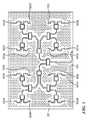
図2を参照するに、特定の一例において、AESA100はタイル200のアレイ(例えば、タイル200の9×9アレイ)を含む。タイル200は、“良品保証タイル(known good tiles)”(KGT)としても知られている。AESA100はまた、冷却板204及びプリント回路基板(PCB)206を含んでいる。一例において、各タイル200がPCB206に取り付けられ、PCB206が冷却板204によって冷却される。各タイル200は、信号を送受信するアクティブ素子222を含んでいる。一例において、アクティブ素子222は8×8アレイに配列される。ここに更に後述するように、タイル200は、酸化物接合(酸化物ボンディング)されたウエハのスタックから製造され、それらが、無線周波数ダイレクトボンドハイブリッド化(radio frequency direct bond hybridization;RF―DBH)及びウエハ貫通ビアを用いて相互接続される。 With reference to FIG. 2, in a particular example, the AESA 100 includes an array of tiles 200 (eg, a 9x9 array of tiles 200). The
図3を参照するに、タイル200は、ウエハ(例えば、ウエハ304a、ウエハ304b、ウエハ304c、及びウエハ304d)、ビームフォーマ312、及びラジエータ/遮蔽構造324を含んでいる。ウエハ304a−304dは酸化物接合されている。例えば、ウエハ304aの酸化物306aがウエハ304bの酸化物306bと接合され、ウエハ304bの酸化物306cがウエハ304cの酸化物306dと接合され、そして、ウエハ304cの酸化物306eがウエハ304dの酸化物306fと接合される。ビームフォーマ312をウエハスタックに接合することにも、酸化物が使用される(例えば、ウエハ304d上の酸化物306gがビームフォーマ312の酸化物306hと接合される)。 With reference to FIG. 3, the
ウエハ304a−304d内にRFマニホールド320が配設されている。特定の一例において、RFマニホールドは、図3に描かれるようにウエハ304a−304dの中央にあるが、図3に示されたもの以外のウエハに置かれてもよい。RFマニホールド320はRFコンバイナ(結合器)/ディバイダ(分配器)として機能する。例えば、64個のアクティブ素子では、マニホールドは64:1のRFコンバイナ/ディバイダである。一例において、ウエハ304a−304d内で、マニホールド320はRF信号のみをルーティングし、特に、ウエハ304a−304d内にDC電力又は制御信号のルーティングは存在しない。マニホールド320はXY平面内で(すなわち、図3の紙面内へと)延在し、マニホールド320の一例が図5にてXY平面内で描かれる。一例において、マニホールド320は、高抵抗率シリコンからなる層を含む。 The
一例において、ウエハ304a−304dは溶融シリカウエハである。特定の一例において、各シリカウエハは100ミクロン厚である。特定の一例において、溶融シリカは低損失の溶融シリカであり、k=3.82であり、損失正接は60GHzで0.0007に等しい。一例において、ウエハ304a−304dは、低損失で高抵抗率のシリコンとし得る。更なる例では、ウエハ304a−304dは、4枚より多い又は少ないウエハとし得る。 In one example, the
タイル200を貫く電気経路を提供するためにビアが使用される。例えば、ウエハ304aはビア(例えば、ビア308a及びビア308b)を含み、ウエハ304bはビア(例えば、ビア308c及びビア308d)を含み、ウエハ304cはビア(例えば、ビア308e、ビア308f、ビア308g、ビア308h、及びビア308i)を含み、そして、ウエハ304dはビア(例えば、ビア308j、ビア308k、ビア308l、ビア308m、及びビア308n)を含む。 Vias are used to provide an electrical path through
ビアは、金属ポストに接続された金属トレースに接続され得る。例えば、ウエハ304aは、金属ポスト313及び金属トレース314を含んでいる。図4にて更に説明するように、金属ポストは、1つのウエハから別の1つのウエハへと電気接続することを提供する。 Vias can be connected to metal traces connected to metal posts. For example,
酸化物接合されたウエハ304a−304dは、電気的な相互接続に使用されるメタライゼーション層を含む。一例において、金属層310aは、ビア308jとビア308kとの間のインターコネクトを提供している。他の一例において、酸化物306dは、ビア308f、ビア308g、及びビア308hの間の電気接続を提供する金属層インターコネクト310bを含んでいる。更なる一例において、酸化物306hは、ビア308mとビア308nとの間の電気接続を提供するインターコネクト310cを含んでいる。ビア308は、ウエハ304の両面の金属を接続し、そのウエハ上の金属パッド間のインターコネクトは、金属ポスト313に示される金属ポストとともに酸化物接合中に作製される。 The oxide-bonded
ビームフォーマ312は、少なくとも1つの制御ASIC(特定用途向け集積回路)(例えば、ASIC340)、増幅器(例えば、増幅器344a及び増幅器344b)、及び位相シフタ(例えば、位相シフタ346a及び位相シフタ346b)を含んでいる。一例において、ビームフォーマ312はシリコンゲルマニウム(SiGe)ウエハ上に製造される。他の例では、ビームフォーマ312はRF減衰及びRFスイッチを提供する。 The
ビームフォーマ312はまた、標準的な表面実装技術を用いたPCB206への取り付けを可能にするために、インターコネクトパッド348bを含む裏面再配線層(RDL)(例えば、RDL348a)を含んでいる。ビームフォーマ312は、はんだバンプ(例えば、はんだバンプ350a−350e)によってPCB206に取り付けられる。一例において、はんだバンプ350aは制御信号を搬送し、はんだバンプ350b、350dはグランドに取り付けられ、はんだバンプ350cはRF信号を搬送し、そして、はんだバンプ350eは電力を搬送する。 The
ラジエータ/遮蔽構造324は、金属インターコネクトによって上記ウエハに接合される。一例において、このインターコネクトははんだバンプとし得る。他の一例において、それはインジウムバンプであってもよい。例えば、ラジエータ/遮蔽構造324は、はんだバンプ380aによってウエハ304aのビア308aに接合され、また、ラジエータ/遮蔽構造324は、はんだバンプ380bによってウエハ304aのビア308bに接合される。一例において、ラジエータ/遮蔽構造324は、ラジエータを通じてRF信号を伝播するとともに、ビームフォーマ312のための放射線シールドを提供するように設計される。一例において、ラジエータは、ウエハスタックへの接続の応力を軽減するために低い膨張係数を持つとともに、正しい放射線遮蔽量を提供するのに十分な厚さの金属で作製される。 The radiator /
特定の一例において、RF信号経路370は、ラジエータ/遮蔽構造324で始まり、接続380b、ウエハ304aのビア308b、ウエハ304bのビア308d、ウエハ304cのビア308i、及びウエハ304dのビア308nを通って続く。RF信号経路370は、増幅器344b及び位相シフタ346bを通り抜けることによってビームフォーマ312内に続く。RF信号は、ウエハ304dのビア308m、ウエハ304cのビア308hを通り抜けることによって、ビームフォーマ312から離れてウエハ304c、304d内に戻るように続く。RF信号経路370は、インターコネクト310b、ウエハ304cのビア308g、ウエハ304dのビア308iを通って続く。RF信号は、ビームフォーマ312内に戻ってビア342を通り、バンプ350cを通ってPCB206へと伝播する。 In a particular example, the
RF経路370は、これらのウエハ内で少なくとも2つの軸の方向に移る。例えば、RF信号経路370は、2つの軸に沿って移る(例えば、それはX軸及びZ軸に沿って移る)。他の例では、信号経路370はY軸(図示せず)の方向にも移り得る。他の例では、RF信号経路は、RF信号経路370とは逆向きに流れ得る。他のRF信号経路は、信号経路370によって限定されない。すなわち、他のRF信号経路及び組み合わせが可能であり、RF信号経路370は、図3において可能な多数のRF信号経路のうちの単なる一例である。 The
図4は、例えば酸化物接合されたウエハ304a−304dが構成されるように酸化物接合される2つのウエハの一例を示している。例えば、ウエハ404aの酸化物406aが、ウエハ404bの酸化物406bに接合される。一例において、酸化物接合は、室温で形成される分子結合である。DBHは、例えば、ウエハ404bのポスト412cに接合されたウエハ404aのポスト412a、及びウエハ404bのポスト412dに接合されたウエハ404aのポスト412bなどの、金属ポストを含む。一例において、ポスト412a−412dは金属で作製される。特定の一例において、ポスト412a−412dは銅ポストである。他の特定の一例において、ポスト412a−412dはニッケルポストである。特定の更なる一例において、ポスト412a−412dはアルミニウムポストである。一例において、ポスト412a−412dは、10ミクロン未満のピッチ能力を有する。 FIG. 4 shows an example of two wafers that are oxide-bonded so as to form, for example, oxide-bonded
ポスト同士が金属トレース層によって接続され得る(例えば、ポスト412cが、金属トレース層414によってポスト412dに接続される)。金属トレース層はビアに接続され得る(例えば、金属トレース層414はビア408に接続される)。一例において、ビア408は、直径において約25ミクロンとし得る。一例において、ビア408は銅ビアとし得る。 The posts may be connected to each other by a metal trace layer (eg, the post 412c is connected to the post 412d by a metal trace layer 414). The metal trace layer can be connected to the via (eg, the
図5は、RFマニホールド320の一例がRFマニホールド520であることを示している。この例において、RFマニホールド520は、16素子(例えば、アクティブ素子522a−522p)用の16:1のRFコンバイナ/ディバイダである。一例において、マニホールド520は、低損失で高抵抗率のシリコンであるウエハ304a−304d内に製造される。 FIG. 5 shows that an example of the
ここに記載したプロセスは、記載した特定の実施形態に限定されるものではない。ここに記載した複数の異なる実施形態の要素を組み合わせて、具体的には上述していない他の実施形態を形成してもよい。ここでは具体的に記載されていない他の実施形態も、以下の請求項の範囲内にある。 The process described herein is not limited to the particular embodiments described. The elements of a plurality of different embodiments described herein may be combined to form other embodiments not specifically described above. Other embodiments not specifically described here are also within the scope of the following claims.
Claims (17)
Translated fromJapanese前記ラジエータ構造に取り付けられ、無線周波数(RF)マニホールド及びビームフォーマを有した、酸化物接合された半導体ウエハと、
を有し、
前記酸化物接合されたウエハを通るRF信号経路が、前記ビームフォーマに向かって伝播する第1部分と、前記ビームフォーマに対して平行に伝播する第2部分とを有する、
アクティブ電子走査アレイ(AESA)タイル。Radiator structure and
An oxide-bonded semiconductor wafer mounted on the radiator structure and having a radio frequency (RF) manifold and a beamformer.
Have,
The RF signal path through the oxide-bonded wafer has a first portion that propagates toward the beamformer and a second portion that propagates parallel to the beamformer.
Active Electronically Scanned Array (AESA) tiles.
1つのウエハからの金属ポストが、他のウエハの金属ポストに接続されている、
請求項1に記載のAESAタイル。The oxide-bonded wafer has a metal post and has a metal post.
A metal post from one wafer is connected to a metal post on another wafer,
The AESA tile according to claim 1.
Applications Claiming Priority (3)
| Application Number | Priority Date | Filing Date | Title |
|---|---|---|---|
| US15/381,286US10541461B2 (en) | 2016-12-16 | 2016-12-16 | Tile for an active electronically scanned array (AESA) |
| US15/381,286 | 2016-12-16 | ||
| PCT/US2017/054836WO2018111386A1 (en) | 2016-12-16 | 2017-10-03 | Tile for an active electronically scanned array (aesa) |
Publications (2)
| Publication Number | Publication Date |
|---|---|
| JP2020502782A JP2020502782A (en) | 2020-01-23 |
| JP6763087B2true JP6763087B2 (en) | 2020-09-30 |
Family
ID=60120186
Family Applications (1)
| Application Number | Title | Priority Date | Filing Date |
|---|---|---|---|
| JP2019525735AActiveJP6763087B2 (en) | 2016-12-16 | 2017-10-03 | Tiles for Active Electronically Scanned Array (AESA) |
Country Status (7)
| Country | Link |
|---|---|
| US (1) | US10541461B2 (en) |
| EP (1) | EP3555961B1 (en) |
| JP (1) | JP6763087B2 (en) |
| KR (1) | KR102193899B1 (en) |
| CN (1) | CN109891674B (en) |
| TW (1) | TWI690970B (en) |
| WO (1) | WO2018111386A1 (en) |
Families Citing this family (23)
| Publication number | Priority date | Publication date | Assignee | Title |
|---|---|---|---|---|
| US20170237180A1 (en) | 2015-09-18 | 2017-08-17 | Anokiwave, Inc. | Laminar Phased Array Antenna |
| US10879608B2 (en)* | 2016-09-13 | 2020-12-29 | The Board Of Regents Of The University Of Oklahoma | Radio frequency scanner |
| US10367256B2 (en)* | 2017-06-26 | 2019-07-30 | Avl Technologies, Inc. | Active electronically steered array for satellite communications |
| US10763566B2 (en)* | 2017-07-20 | 2020-09-01 | Apple Inc. | Millimeter wave transmission line structures |
| US10361485B2 (en) | 2017-08-04 | 2019-07-23 | Raytheon Company | Tripole current loop radiating element with integrated circularly polarized feed |
| US11418971B2 (en)* | 2017-12-24 | 2022-08-16 | Anokiwave, Inc. | Beamforming integrated circuit, AESA system and method |
| US10998640B2 (en) | 2018-05-15 | 2021-05-04 | Anokiwave, Inc. | Cross-polarized time division duplexed antenna |
| WO2019222474A1 (en)* | 2018-05-18 | 2019-11-21 | Raytheon Company | Additive manufactured reactive beamformer |
| US11495877B2 (en)* | 2018-08-17 | 2022-11-08 | Metawave Corporation | Multi-layer, multi-steering antenna system for autonomous vehicles |
| US11121302B2 (en) | 2018-10-11 | 2021-09-14 | SeeQC, Inc. | System and method for superconducting multi-chip module |
| US10840197B2 (en)* | 2018-10-30 | 2020-11-17 | Taiwan Semiconductor Manufacturing Company, Ltd. | Package structure and manufacturing method thereof |
| US11557545B2 (en)* | 2018-12-04 | 2023-01-17 | Qorvo Us, Inc. | Monolithic microwave integrated circuit (MMIC) with embedded transmission line (ETL) ground shielding |
| CN110379799B (en)* | 2019-07-18 | 2020-04-03 | 武汉新芯集成电路制造有限公司 | Chip structure, wafer structure and manufacturing method thereof |
| US11183758B2 (en)* | 2019-07-23 | 2021-11-23 | Rockwell Collins, Inc. | System and method for active electronically scanned array with multi-band multi-beam architecture |
| CN110739537B (en)* | 2019-09-28 | 2021-06-15 | 西南电子技术研究所(中国电子科技集团公司第十研究所) | High-density high-integration millimeter wave tile-type phase-controlled antenna T/R assembly |
| US11049824B2 (en)* | 2019-10-17 | 2021-06-29 | Viasat, Inc. | Antenna apparatus with integrated antenna array and low loss multi-layer interposer |
| US11296424B2 (en)* | 2020-01-21 | 2022-04-05 | Rockwell Collins, Inc. | Bump mounted radiating element architecture |
| CN111740232B (en)* | 2020-08-26 | 2020-11-17 | 成都瑞迪威科技有限公司 | Feed structure of tile-type phased-array antenna and processing method thereof |
| CN112103637B (en)* | 2020-08-30 | 2022-09-02 | 西南电子技术研究所(中国电子科技集团公司第十研究所) | Modularized satellite-borne Ka-frequency-band active phased-array antenna system |
| KR20220141013A (en)* | 2021-04-12 | 2022-10-19 | 삼성전자주식회사 | Antenna structure including phase shifter and electronic device including same |
| KR20220158967A (en) | 2021-05-25 | 2022-12-02 | 삼성전자주식회사 | Antenna module and electronic apparatus comprising the same |
| US12406901B2 (en) | 2021-09-02 | 2025-09-02 | Raytheon Company | Wafer-scale direct bonded array core block for an active electronically steerable array (AESA) |
| US11870142B2 (en) | 2021-09-17 | 2024-01-09 | Raytheon Company | Tile to tile RF grounding |
Family Cites Families (107)
| Publication number | Priority date | Publication date | Assignee | Title |
|---|---|---|---|---|
| US2015028A (en) | 1932-04-12 | 1935-09-17 | Us Ind Alcohol Co | Holder for advertising material |
| US3528050A (en) | 1969-05-02 | 1970-09-08 | Holub Ind Inc | Push-on type grounding clip |
| US4690471A (en) | 1986-05-19 | 1987-09-01 | Motorola, Inc. | RF interconnect with triaxial self-alignment |
| JP2525545Y2 (en) | 1990-06-27 | 1997-02-12 | 日本電業工作株式会社 | Broadband microstrip antenna |
| US5172082A (en) | 1991-04-19 | 1992-12-15 | Hughes Aircraft Company | Multi-octave bandwidth balun |
| JPH0567912A (en) | 1991-04-24 | 1993-03-19 | Matsushita Electric Works Ltd | Flat antenna |
| FR2683952A1 (en) | 1991-11-14 | 1993-05-21 | Dassault Electronique | IMPROVED MICRO-TAPE ANTENNA DEVICE, PARTICULARLY FOR TELEPHONE TRANSMISSIONS BY SATELLITE. |
| US5410281A (en) | 1993-03-09 | 1995-04-25 | Sierra Technologies, Inc. | Microwave high power combiner/divider |
| JPH07106841A (en) | 1993-10-06 | 1995-04-21 | Mitsubishi Electric Corp | Printed dipole antenna |
| US5434575A (en) | 1994-01-28 | 1995-07-18 | California Microwave, Inc. | Phased array antenna system using polarization phase shifting |
| US5455546A (en) | 1994-09-22 | 1995-10-03 | Glenayre Electronics, Inc. | High power radio frequency divider/combiner |
| US5644277A (en) | 1995-02-27 | 1997-07-01 | Hughes Aircraft Company | Three-wire-line vertical interconnect structure for multilevel substrates |
| US5603620A (en) | 1995-08-04 | 1997-02-18 | Delco Electronics Corp. | Integrated printed circuit connector and ground clip assembly |
| AU2567797A (en) | 1996-04-03 | 1997-10-29 | Johan Granholm | Dual polarization antenna array with very low cross polarization and low side lobes |
| US6184832B1 (en) | 1996-05-17 | 2001-02-06 | Raytheon Company | Phased array antenna |
| US5745079A (en) | 1996-06-28 | 1998-04-28 | Raytheon Company | Wide-band/dual-band stacked-disc radiators on stacked-dielectric posts phased array antenna |
| US5880694A (en) | 1997-06-18 | 1999-03-09 | Hughes Electronics Corporation | Planar low profile, wideband, wide-scan phased array antenna using a stacked-disc radiator |
| US5886590A (en) | 1997-09-04 | 1999-03-23 | Hughes Electronics Corporation | Microstrip to coax vertical launcher using fuzz button and solderless interconnects |
| JP3556832B2 (en)* | 1998-05-22 | 2004-08-25 | 三菱電機株式会社 | Phased array antenna |
| US6114997A (en) | 1998-05-27 | 2000-09-05 | Raytheon Company | Low-profile, integrated radiator tiles for wideband, dual-linear and circular-polarized phased array applications |
| JP2000312112A (en) | 1998-09-22 | 2000-11-07 | Matsushita Electric Ind Co Ltd | Patch antenna device |
| US6320542B1 (en) | 1998-09-22 | 2001-11-20 | Matsushita Electric Industrial Co., Ltd. | Patch antenna apparatus with improved projection area |
| US6100775A (en) | 1998-10-15 | 2000-08-08 | Raytheon Company | Vertical interconnect circuit for coplanar waveguides |
| AU2001296876A1 (en) | 2000-09-15 | 2002-03-26 | Raytheon Company | Microelectromechanical phased array antenna |
| US6512487B1 (en) | 2000-10-31 | 2003-01-28 | Harris Corporation | Wideband phased array antenna and associated methods |
| US6429816B1 (en) | 2001-05-04 | 2002-08-06 | Harris Corporation | Spatially orthogonal signal distribution and support architecture for multi-beam phased array antenna |
| US6459415B1 (en) | 2001-05-14 | 2002-10-01 | Eleven Engineering Inc. | Omni-directional planar antenna design |
| US6580402B2 (en) | 2001-07-26 | 2003-06-17 | The Boeing Company | Antenna integrated ceramic chip carrier for a phased array antenna |
| US6867742B1 (en) | 2001-09-04 | 2005-03-15 | Raytheon Company | Balun and groundplanes for decade band tapered slot antenna, and method of making same |
| US20030112200A1 (en) | 2001-12-17 | 2003-06-19 | Alcatel, Radio Frequency Systems, Inc. | Horizontally polarized printed circuit antenna array |
| US6935866B2 (en) | 2002-04-02 | 2005-08-30 | Adc Telecommunications, Inc. | Card edge coaxial connector |
| US6882247B2 (en) | 2002-05-15 | 2005-04-19 | Raytheon Company | RF filtered DC interconnect |
| US7193390B2 (en) | 2002-05-17 | 2007-03-20 | Sony Corporation | Apparatus for connecting secondary battery cells in series and method for controlling secondary battery cells connected in series |
| US6664867B1 (en) | 2002-07-19 | 2003-12-16 | Paratek Microwave, Inc. | Tunable electromagnetic transmission structure for effecting coupling of electromagnetic signals |
| US6686885B1 (en) | 2002-08-09 | 2004-02-03 | Northrop Grumman Corporation | Phased array antenna for space based radar |
| JP4181173B2 (en) | 2002-10-24 | 2008-11-12 | サントル ナシオナル ドゥ ラ ルシェルシェサイアンティフィク(セエヌエールエス) | Multi-beam PBG material antenna |
| US6975267B2 (en) | 2003-02-05 | 2005-12-13 | Northrop Grumman Corporation | Low profile active electronically scanned antenna (AESA) for Ka-band radar systems |
| US7180457B2 (en) | 2003-07-11 | 2007-02-20 | Raytheon Company | Wideband phased array radiator |
| ATE396516T1 (en) | 2003-07-25 | 2008-06-15 | Stichting Astron | DOUBLE POLARIZED ANTENNA ARRANGEMENT AND PROCESS FOR PRODUCTION THEREOF |
| US6856297B1 (en) | 2003-08-04 | 2005-02-15 | Harris Corporation | Phased array antenna with discrete capacitive coupling and associated methods |
| US6876336B2 (en) | 2003-08-04 | 2005-04-05 | Harris Corporation | Phased array antenna with edge elements and associated methods |
| US7315288B2 (en) | 2004-01-15 | 2008-01-01 | Raytheon Company | Antenna arrays using long slot apertures and balanced feeds |
| US6977623B2 (en) | 2004-02-17 | 2005-12-20 | Harris Corporation | Wideband slotted phased array antenna and associated methods |
| US7272880B1 (en) | 2004-05-27 | 2007-09-25 | Lockheed Martin Corporation | Distributed load edge clamp |
| US7012572B1 (en) | 2004-07-16 | 2006-03-14 | Hrl Laboratories, Llc | Integrated ultra wideband element card for array antennas |
| US7113142B2 (en) | 2004-10-21 | 2006-09-26 | The Boeing Company | Design and fabrication methodology for a phased array antenna with integrated feed structure-conformal load-bearing concept |
| US7109942B2 (en) | 2004-10-21 | 2006-09-19 | The Boeing Company | Structurally integrated phased array antenna aperture design and fabrication method |
| US7138952B2 (en) | 2005-01-11 | 2006-11-21 | Raytheon Company | Array antenna with dual polarization and method |
| US7084827B1 (en) | 2005-02-07 | 2006-08-01 | Harris Corporation | Phased array antenna with an impedance matching layer and associated methods |
| JP5088135B2 (en) | 2005-10-18 | 2012-12-05 | 日本電気株式会社 | Vertical signal path, printed circuit board having the same, and semiconductor package having the printed circuit board and a semiconductor element |
| US7358921B2 (en) | 2005-12-01 | 2008-04-15 | Harris Corporation | Dual polarization antenna and associated methods |
| US7221322B1 (en) | 2005-12-14 | 2007-05-22 | Harris Corporation | Dual polarization antenna array with inter-element coupling and associated methods |
| US7411472B1 (en) | 2006-02-01 | 2008-08-12 | Rockwell Collins, Inc. | Low-loss integrated waveguide feed for wafer-scale heterogeneous layered active electronically scanned array |
| US8373597B2 (en) | 2006-08-09 | 2013-02-12 | Spx Corporation | High-power-capable circularly polarized patch antenna apparatus and method |
| US9172145B2 (en)* | 2006-09-21 | 2015-10-27 | Raytheon Company | Transmit/receive daughter card with integral circulator |
| US9019166B2 (en)* | 2009-06-15 | 2015-04-28 | Raytheon Company | Active electronically scanned array (AESA) card |
| US7671696B1 (en)* | 2006-09-21 | 2010-03-02 | Raytheon Company | Radio frequency interconnect circuits and techniques |
| US8279131B2 (en)* | 2006-09-21 | 2012-10-02 | Raytheon Company | Panel array |
| US7489283B2 (en)* | 2006-12-22 | 2009-02-10 | The Boeing Company | Phased array antenna apparatus and methods of manufacture |
| US20080169992A1 (en) | 2007-01-16 | 2008-07-17 | Harris Corporation | Dual-polarization, slot-mode antenna and associated methods |
| EP2372756A1 (en) | 2007-03-13 | 2011-10-05 | Semiconductor Energy Laboratory Co, Ltd. | Semiconductor device and manufacturing method thereof |
| US7948441B2 (en) | 2007-04-12 | 2011-05-24 | Raytheon Company | Low profile antenna |
| US7688265B2 (en) | 2007-09-18 | 2010-03-30 | Raytheon Company | Dual polarized low profile antenna |
| US7579997B2 (en) | 2007-10-03 | 2009-08-25 | The Boeing Company | Advanced antenna integrated printed wiring board with metallic waveguide plate |
| US8031126B2 (en) | 2007-11-13 | 2011-10-04 | Raytheon Company | Dual polarized antenna |
| GB0724684D0 (en) | 2007-12-18 | 2009-01-07 | Bae Systems Plc | Anntenna Feed Module |
| CN201562835U (en) | 2008-09-09 | 2010-08-25 | 莫列斯公司 | Shielding cover and connector component thereof |
| US8706049B2 (en)* | 2008-12-31 | 2014-04-22 | Intel Corporation | Platform integrated phased array transmit/receive module |
| CN102405564B (en) | 2009-02-18 | 2014-09-03 | 莫列斯公司 | Vertical Connectors for Printed Circuit Boards |
| IL197906A (en) | 2009-04-05 | 2014-09-30 | Elta Systems Ltd | Phased array antennas and method for producing them |
| US8325093B2 (en) | 2009-07-31 | 2012-12-04 | University Of Massachusetts | Planar ultrawideband modular antenna array |
| US20110089531A1 (en) | 2009-10-16 | 2011-04-21 | Teledyne Scientific & Imaging, Llc | Interposer Based Monolithic Microwave Integrate Circuit (iMMIC) |
| DE112010002548A5 (en) | 2009-12-17 | 2012-08-23 | Conti Temic Microelectronic Gmbh | CIRCUIT BOARD WITH MULTIPLE COUPLED PLATE LAYERS WITH A BARE-DIE MOUNTING FOR OPERATION AS A GEARBOX CONTROLLER |
| WO2012044219A1 (en)* | 2010-10-01 | 2012-04-05 | Saab Ab | Mounting system for transmitter receiver modules |
| KR20120035394A (en) | 2010-10-05 | 2012-04-16 | 삼성전자주식회사 | Apparatus for system-on-package using vertical transmission line transition and land grid array connection |
| US8542151B2 (en) | 2010-10-21 | 2013-09-24 | Mediatek Inc. | Antenna module and antenna unit thereof |
| US8547275B2 (en)* | 2010-11-29 | 2013-10-01 | Src, Inc. | Active electronically scanned array antenna for hemispherical scan coverage |
| US8928544B2 (en) | 2011-02-21 | 2015-01-06 | Her Majesty The Queen In Right Of Canada As Represented By The Minister Of National Defence | Wideband circularly polarized hybrid dielectric resonator antenna |
| US9112270B2 (en) | 2011-06-02 | 2015-08-18 | Brigham Young Univeristy | Planar array feed for satellite communications |
| US9112262B2 (en) | 2011-06-02 | 2015-08-18 | Brigham Young University | Planar array feed for satellite communications |
| US20130026586A1 (en) | 2011-07-26 | 2013-01-31 | Texas Instruments Incorporated | Cross-loop antenna |
| US8786515B2 (en) | 2011-08-30 | 2014-07-22 | Harris Corporation | Phased array antenna module and method of making same |
| TWI449475B (en) | 2012-01-09 | 2014-08-11 | Novatek Microelectronics Corp | Printed circuit board |
| US8648454B2 (en) | 2012-02-14 | 2014-02-11 | International Business Machines Corporation | Wafer-scale package structures with integrated antennas |
| US8780561B2 (en) | 2012-03-30 | 2014-07-15 | Raytheon Company | Conduction cooling of multi-channel flip chip based panel array circuits |
| US9054410B2 (en) | 2012-05-24 | 2015-06-09 | Commscope Technologies Llc | Dipole strength clip |
| US9537208B2 (en) | 2012-11-12 | 2017-01-03 | Raytheon Company | Dual polarization current loop radiator with integrated balun |
| US10403511B2 (en) | 2013-01-14 | 2019-09-03 | Intel Corporation | Backside redistribution layer patch antenna |
| US8921992B2 (en)* | 2013-03-14 | 2014-12-30 | Raytheon Company | Stacked wafer with coolant channels |
| US9343816B2 (en) | 2013-04-09 | 2016-05-17 | Raytheon Company | Array antenna and related techniques |
| CN105393403B (en) | 2013-07-08 | 2018-06-26 | 高通股份有限公司 | Techniques for Operating Phased Array Antennas in mmWave Radio Modules |
| US9136572B2 (en) | 2013-07-26 | 2015-09-15 | Raytheon Company | Dual stripline tile circulator utilizing thick film post-fired substrate stacking |
| US9437929B2 (en) | 2014-01-15 | 2016-09-06 | Raytheon Company | Dual polarized array antenna with modular multi-balun board and associated methods |
| US9472859B2 (en) | 2014-05-20 | 2016-10-18 | International Business Machines Corporation | Integration of area efficient antennas for phased array or wafer scale array antenna applications |
| CN104332413A (en)* | 2014-05-30 | 2015-02-04 | 中国电子科技集团公司第十研究所 | 3D assembling method for integrally integrating chips of T/R assembly |
| CN104022321B (en)* | 2014-05-30 | 2016-04-20 | 中国电子科技集团公司第二十研究所 | A kind of miniature tile type T/R assembly based on LTCC |
| US9688529B2 (en)* | 2014-06-10 | 2017-06-27 | Qorvo Us, Inc. | Glass wafer assembly |
| US10050351B2 (en) | 2014-06-18 | 2018-08-14 | X-Celeprint Limited | Multilayer printed capacitors |
| TWI577085B (en)* | 2014-10-03 | 2017-04-01 | 雷森公司 | Transmit/receive daughter card with integral circulator and modular scalable radio frequency(rf) circuit card array(cca) |
| US9402301B2 (en) | 2014-12-10 | 2016-07-26 | Raytheon Company | Vertical radio frequency module |
| US10297923B2 (en)* | 2014-12-12 | 2019-05-21 | The Boeing Company | Switchable transmit and receive phased array antenna |
| EP3262711B1 (en) | 2015-02-26 | 2020-11-18 | The Government of the United States of America as represented by the Secretary of the Navy | Planar ultrawideband modular antenna array having improved bandwidth |
| US9490519B2 (en) | 2015-03-19 | 2016-11-08 | James D Lilly | Transmission line transformer antenna |
| CN204857954U (en) | 2015-08-06 | 2015-12-09 | 中国电子科技集团公司第三十八研究所 | A Ka-band wide-angle scanning phased array antenna |
| CN108604732B (en) | 2015-11-17 | 2020-09-08 | 深谷波股份公司 | Self-grounded surface-mountable bowtie antenna assembly, antenna lobe and method of manufacture |
| US10490907B2 (en) | 2016-09-27 | 2019-11-26 | Google Llc | Suppression of surface waves in printed circuit board-based phased-array antennas |
| US10361485B2 (en) | 2017-08-04 | 2019-07-23 | Raytheon Company | Tripole current loop radiating element with integrated circularly polarized feed |
- 2016
- 2016-12-16USUS15/381,286patent/US10541461B2/enactiveActive
- 2017
- 2017-10-03CNCN201780066115.2Apatent/CN109891674B/enactiveActive
- 2017-10-03WOPCT/US2017/054836patent/WO2018111386A1/ennot_activeCeased
- 2017-10-03JPJP2019525735Apatent/JP6763087B2/enactiveActive
- 2017-10-03EPEP17785128.4Apatent/EP3555961B1/enactiveActive
- 2017-10-03KRKR1020197010632Apatent/KR102193899B1/enactiveActive
- 2017-10-17TWTW106135418Apatent/TWI690970B/enactive
Also Published As
| Publication number | Publication date |
|---|---|
| EP3555961B1 (en) | 2021-04-28 |
| CN109891674A (en) | 2019-06-14 |
| CN109891674B (en) | 2021-08-24 |
| WO2018111386A1 (en) | 2018-06-21 |
| KR20190045941A (en) | 2019-05-03 |
| TWI690970B (en) | 2020-04-11 |
| EP3555961A1 (en) | 2019-10-23 |
| JP2020502782A (en) | 2020-01-23 |
| US10541461B2 (en) | 2020-01-21 |
| TW201824330A (en) | 2018-07-01 |
| US20180175476A1 (en) | 2018-06-21 |
| KR102193899B1 (en) | 2020-12-23 |
Similar Documents
| Publication | Publication Date | Title |
|---|---|---|
| JP6763087B2 (en) | Tiles for Active Electronically Scanned Array (AESA) | |
| EP3032651B1 (en) | Switchable transmit and receive phased array antenna | |
| US9985346B2 (en) | Wireless communications package with integrated antennas and air cavity | |
| US8643548B2 (en) | Dual beam dual selectable polarization antenna | |
| Patterson et al. | A 60-GHz active receiving switched-beam antenna array with integrated butler matrix and GaAs amplifiers | |
| US7619567B2 (en) | Integrated phased array antenna | |
| KR102802028B1 (en) | Antenna device having integrated antenna array and low-loss multilayer interposer | |
| JP2017200168A (en) | Scalable planar mounting architecture for active scanning phased array antenna system | |
| WO2019187758A1 (en) | Array antenna | |
| US7411472B1 (en) | Low-loss integrated waveguide feed for wafer-scale heterogeneous layered active electronically scanned array | |
| JP2023546519A (en) | Integrated antenna array with beamformer IC chip with multiple surface boundaries | |
| JP6067445B2 (en) | Radar equipment | |
| TWI765132B (en) | Antenna structure | |
| JP6341983B2 (en) | Radar equipment | |
| US12193151B2 (en) | High-frequency circuit board and antenna module | |
| WO2024206457A1 (en) | Phased array antennas employing antenna element system in package |
Legal Events
| Date | Code | Title | Description |
|---|---|---|---|
| A621 | Written request for application examination | Free format text:JAPANESE INTERMEDIATE CODE: A621 Effective date:20190514 | |
| TRDD | Decision of grant or rejection written | ||
| A01 | Written decision to grant a patent or to grant a registration (utility model) | Free format text:JAPANESE INTERMEDIATE CODE: A01 Effective date:20200811 | |
| A61 | First payment of annual fees (during grant procedure) | Free format text:JAPANESE INTERMEDIATE CODE: A61 Effective date:20200909 | |
| R150 | Certificate of patent or registration of utility model | Ref document number:6763087 Country of ref document:JP Free format text:JAPANESE INTERMEDIATE CODE: R150 | |
| R250 | Receipt of annual fees | Free format text:JAPANESE INTERMEDIATE CODE: R250 | |
| R250 | Receipt of annual fees | Free format text:JAPANESE INTERMEDIATE CODE: R250 |