JP6739185B2 - Storage system and storage control circuit - Google Patents
Storage system and storage control circuitDownload PDFInfo
- Publication number
- JP6739185B2 JP6739185B2JP2016027995AJP2016027995AJP6739185B2JP 6739185 B2JP6739185 B2JP 6739185B2JP 2016027995 AJP2016027995 AJP 2016027995AJP 2016027995 AJP2016027995 AJP 2016027995AJP 6739185 B2JP6739185 B2JP 6739185B2
- Authority
- JP
- Japan
- Prior art keywords
- transistor
- insulating layer
- data
- oxide semiconductor
- storage
- Prior art date
- Legal status (The legal status is an assumption and is not a legal conclusion. Google has not performed a legal analysis and makes no representation as to the accuracy of the status listed.)
- Expired - Fee Related
Links
- 238000003860storageMethods0.000titleclaimsdescription186
- 239000004065semiconductorSubstances0.000claimsdescription162
- 230000006870functionEffects0.000claimsdescription29
- 239000003990capacitorSubstances0.000claimsdescription26
- 230000015572biosynthetic processEffects0.000claimsdescription15
- 239000010410layerSubstances0.000description297
- 239000010408filmSubstances0.000description136
- 239000013078crystalSubstances0.000description53
- 239000007789gasSubstances0.000description38
- 239000011701zincSubstances0.000description38
- 238000000034methodMethods0.000description29
- 239000000758substrateSubstances0.000description26
- 239000012535impuritySubstances0.000description22
- QVGXLLKOCUKJST-UHFFFAOYSA-Natomic oxygenChemical compound[O]QVGXLLKOCUKJST-UHFFFAOYSA-N0.000description21
- 229910052760oxygenInorganic materials0.000description21
- 239000001301oxygenSubstances0.000description21
- 238000010586diagramMethods0.000description19
- IJGRMHOSHXDMSA-UHFFFAOYSA-NAtomic nitrogenChemical compoundN#NIJGRMHOSHXDMSA-UHFFFAOYSA-N0.000description18
- 229910052739hydrogenInorganic materials0.000description15
- 239000001257hydrogenSubstances0.000description15
- XUIMIQQOPSSXEZ-UHFFFAOYSA-NSiliconChemical compound[Si]XUIMIQQOPSSXEZ-UHFFFAOYSA-N0.000description14
- 229910052710siliconInorganic materials0.000description14
- 239000010703siliconSubstances0.000description14
- 229910052751metalInorganic materials0.000description13
- 239000000203mixtureSubstances0.000description13
- 239000011229interlayerSubstances0.000description12
- 238000002173high-resolution transmission electron microscopyMethods0.000description11
- 239000004020conductorSubstances0.000description10
- 238000002955isolationMethods0.000description10
- 239000002184metalSubstances0.000description10
- UFHFLCQGNIYNRP-UHFFFAOYSA-NHydrogenChemical compound[H][H]UFHFLCQGNIYNRP-UHFFFAOYSA-N0.000description9
- 229910052757nitrogenInorganic materials0.000description9
- XKRFYHLGVUSROY-UHFFFAOYSA-NArgonChemical compound[Ar]XKRFYHLGVUSROY-UHFFFAOYSA-N0.000description8
- 229910052782aluminiumInorganic materials0.000description8
- XAGFODPZIPBFFR-UHFFFAOYSA-NaluminiumChemical compound[Al]XAGFODPZIPBFFR-UHFFFAOYSA-N0.000description8
- 239000002356single layerSubstances0.000description8
- VYPSYNLAJGMNEJ-UHFFFAOYSA-NSilicium dioxideChemical compoundO=[Si]=OVYPSYNLAJGMNEJ-UHFFFAOYSA-N0.000description7
- 238000004458analytical methodMethods0.000description7
- 230000000903blocking effectEffects0.000description7
- 230000007547defectEffects0.000description7
- 230000000694effectsEffects0.000description7
- 239000002994raw materialSubstances0.000description7
- 229910052581Si3N4Inorganic materials0.000description6
- 238000000231atomic layer depositionMethods0.000description6
- 150000001875compoundsChemical class0.000description6
- 239000000470constituentSubstances0.000description6
- 238000002003electron diffractionMethods0.000description6
- 150000002431hydrogenChemical class0.000description6
- HQVNEWCFYHHQES-UHFFFAOYSA-Nsilicon nitrideChemical compoundN12[Si]34N5[Si]62N3[Si]51N64HQVNEWCFYHHQES-UHFFFAOYSA-N0.000description6
- 229910052814silicon oxideInorganic materials0.000description6
- RYGMFSIKBFXOCR-UHFFFAOYSA-NCopperChemical compound[Cu]RYGMFSIKBFXOCR-UHFFFAOYSA-N0.000description5
- GYHNNYVSQQEPJS-UHFFFAOYSA-NGalliumChemical compound[Ga]GYHNNYVSQQEPJS-UHFFFAOYSA-N0.000description5
- 230000008859changeEffects0.000description5
- 229910052802copperInorganic materials0.000description5
- 239000010949copperSubstances0.000description5
- 230000007423decreaseEffects0.000description5
- 229910052733galliumInorganic materials0.000description5
- 239000011261inert gasSubstances0.000description5
- 239000000126substanceSubstances0.000description5
- 238000002230thermal chemical vapour depositionMethods0.000description5
- WFKWXMTUELFFGS-UHFFFAOYSA-NtungstenChemical compound[W]WFKWXMTUELFFGS-UHFFFAOYSA-N0.000description5
- 229910052721tungstenInorganic materials0.000description5
- 239000010937tungstenSubstances0.000description5
- OKTJSMMVPCPJKN-UHFFFAOYSA-NCarbonChemical compound[C]OKTJSMMVPCPJKN-UHFFFAOYSA-N0.000description4
- 208000005156DehydrationDiseases0.000description4
- PXHVJJICTQNCMI-UHFFFAOYSA-NNickelChemical compound[Ni]PXHVJJICTQNCMI-UHFFFAOYSA-N0.000description4
- OAICVXFJPJFONN-UHFFFAOYSA-NPhosphorusChemical compound[P]OAICVXFJPJFONN-UHFFFAOYSA-N0.000description4
- XLOMVQKBTHCTTD-UHFFFAOYSA-NZinc monoxideChemical compound[Zn]=OXLOMVQKBTHCTTD-UHFFFAOYSA-N0.000description4
- 229910045601alloyInorganic materials0.000description4
- 239000000956alloySubstances0.000description4
- 229910052786argonInorganic materials0.000description4
- 125000004429atomChemical group0.000description4
- 230000008901benefitEffects0.000description4
- 229910052799carbonInorganic materials0.000description4
- 230000018044dehydrationEffects0.000description4
- 238000006297dehydration reactionMethods0.000description4
- 238000006356dehydrogenation reactionMethods0.000description4
- 229910052735hafniumInorganic materials0.000description4
- VBJZVLUMGGDVMO-UHFFFAOYSA-Nhafnium atomChemical compound[Hf]VBJZVLUMGGDVMO-UHFFFAOYSA-N0.000description4
- 229910052738indiumInorganic materials0.000description4
- 239000012212insulatorSubstances0.000description4
- 229910052746lanthanumInorganic materials0.000description4
- FZLIPJUXYLNCLC-UHFFFAOYSA-Nlanthanum atomChemical compound[La]FZLIPJUXYLNCLC-UHFFFAOYSA-N0.000description4
- 239000000463materialSubstances0.000description4
- 238000005259measurementMethods0.000description4
- PLDDOISOJJCEMH-UHFFFAOYSA-Nneodymium(3+);oxygen(2-)Chemical compound[O-2].[O-2].[O-2].[Nd+3].[Nd+3]PLDDOISOJJCEMH-UHFFFAOYSA-N0.000description4
- 229910052698phosphorusInorganic materials0.000description4
- 239000011574phosphorusSubstances0.000description4
- 239000000523sampleSubstances0.000description4
- 229910052715tantalumInorganic materials0.000description4
- GUVRBAGPIYLISA-UHFFFAOYSA-Ntantalum atomChemical compound[Ta]GUVRBAGPIYLISA-UHFFFAOYSA-N0.000description4
- 229910052727yttriumInorganic materials0.000description4
- VWQVUPCCIRVNHF-UHFFFAOYSA-Nyttrium atomChemical compound[Y]VWQVUPCCIRVNHF-UHFFFAOYSA-N0.000description4
- 229910018137Al-ZnInorganic materials0.000description3
- 229910018573Al—ZnInorganic materials0.000description3
- ZOXJGFHDIHLPTG-UHFFFAOYSA-NBoronChemical compound[B]ZOXJGFHDIHLPTG-UHFFFAOYSA-N0.000description3
- PXGOKWXKJXAPGV-UHFFFAOYSA-NFluorineChemical compoundFFPXGOKWXKJXAPGV-UHFFFAOYSA-N0.000description3
- 229910052779NeodymiumInorganic materials0.000description3
- ATJFFYVFTNAWJD-UHFFFAOYSA-NTinChemical compound[Sn]ATJFFYVFTNAWJD-UHFFFAOYSA-N0.000description3
- RTAQQCXQSZGOHL-UHFFFAOYSA-NTitaniumChemical compound[Ti]RTAQQCXQSZGOHL-UHFFFAOYSA-N0.000description3
- QCWXUUIWCKQGHC-UHFFFAOYSA-NZirconiumChemical compound[Zr]QCWXUUIWCKQGHC-UHFFFAOYSA-N0.000description3
- 229910052796boronInorganic materials0.000description3
- 238000009792diffusion processMethods0.000description3
- AJNVQOSZGJRYEI-UHFFFAOYSA-Ndigallium;oxygen(2-)Chemical compound[O-2].[O-2].[O-2].[Ga+3].[Ga+3]AJNVQOSZGJRYEI-UHFFFAOYSA-N0.000description3
- AXAZMDOAUQTMOW-UHFFFAOYSA-NdimethylzincChemical compoundC[Zn]CAXAZMDOAUQTMOW-UHFFFAOYSA-N0.000description3
- 230000005684electric fieldEffects0.000description3
- 230000005669field effectEffects0.000description3
- 229910052731fluorineInorganic materials0.000description3
- 239000011737fluorineSubstances0.000description3
- 229910001195gallium oxideInorganic materials0.000description3
- 229910052732germaniumInorganic materials0.000description3
- GNPVGFCGXDBREM-UHFFFAOYSA-Ngermanium atomChemical compound[Ge]GNPVGFCGXDBREM-UHFFFAOYSA-N0.000description3
- 229910000449hafnium oxideInorganic materials0.000description3
- WIHZLLGSGQNAGK-UHFFFAOYSA-Nhafnium(4+);oxygen(2-)Chemical compound[O-2].[O-2].[Hf+4]WIHZLLGSGQNAGK-UHFFFAOYSA-N0.000description3
- 125000005843halogen groupChemical group0.000description3
- APFVFJFRJDLVQX-UHFFFAOYSA-Nindium atomChemical compound[In]APFVFJFRJDLVQX-UHFFFAOYSA-N0.000description3
- 239000011777magnesiumSubstances0.000description3
- 238000004519manufacturing processMethods0.000description3
- QEFYFXOXNSNQGX-UHFFFAOYSA-Nneodymium atomChemical compound[Nd]QEFYFXOXNSNQGX-UHFFFAOYSA-N0.000description3
- 230000001151other effectEffects0.000description3
- TWNQGVIAIRXVLR-UHFFFAOYSA-Noxo(oxoalumanyloxy)alumaneChemical compoundO=[Al]O[Al]=OTWNQGVIAIRXVLR-UHFFFAOYSA-N0.000description3
- SIWVEOZUMHYXCS-UHFFFAOYSA-Noxo(oxoyttriooxy)yttriumChemical compoundO=[Y]O[Y]=OSIWVEOZUMHYXCS-UHFFFAOYSA-N0.000description3
- 230000000717retained effectEffects0.000description3
- 239000003381stabilizerSubstances0.000description3
- 238000012916structural analysisMethods0.000description3
- 239000010409thin filmSubstances0.000description3
- 229910052718tinInorganic materials0.000description3
- 229910052719titaniumInorganic materials0.000description3
- 239000010936titaniumSubstances0.000description3
- XCZXGTMEAKBVPV-UHFFFAOYSA-NtrimethylgalliumChemical compoundC[Ga](C)CXCZXGTMEAKBVPV-UHFFFAOYSA-N0.000description3
- XLYOFNOQVPJJNP-UHFFFAOYSA-NwaterSubstancesOXLYOFNOQVPJJNP-UHFFFAOYSA-N0.000description3
- 229910001868waterInorganic materials0.000description3
- 229910052726zirconiumInorganic materials0.000description3
- 229910018120Al-Ga-ZnInorganic materials0.000description2
- CURLTUGMZLYLDI-UHFFFAOYSA-NCarbon dioxideChemical compoundO=C=OCURLTUGMZLYLDI-UHFFFAOYSA-N0.000description2
- ZAMOUSCENKQFHK-UHFFFAOYSA-NChlorine atomChemical compound[Cl]ZAMOUSCENKQFHK-UHFFFAOYSA-N0.000description2
- XEEYBQQBJWHFJM-UHFFFAOYSA-NIronChemical compound[Fe]XEEYBQQBJWHFJM-UHFFFAOYSA-N0.000description2
- FYYHWMGAXLPEAU-UHFFFAOYSA-NMagnesiumChemical compound[Mg]FYYHWMGAXLPEAU-UHFFFAOYSA-N0.000description2
- ZOKXTWBITQBERF-UHFFFAOYSA-NMolybdenumChemical compound[Mo]ZOKXTWBITQBERF-UHFFFAOYSA-N0.000description2
- 229910020833Sn-Al-ZnInorganic materials0.000description2
- 229910020868Sn-Ga-ZnInorganic materials0.000description2
- 238000002441X-ray diffractionMethods0.000description2
- 229910007541Zn OInorganic materials0.000description2
- 230000005540biological transmissionEffects0.000description2
- 238000005229chemical vapour depositionMethods0.000description2
- 229910052801chlorineInorganic materials0.000description2
- 239000000460chlorineSubstances0.000description2
- 238000010894electron beam technologyMethods0.000description2
- 238000005530etchingMethods0.000description2
- -1for exampleChemical compound0.000description2
- YBMRDBCBODYGJE-UHFFFAOYSA-Ngermanium oxideInorganic materialsO=[Ge]=OYBMRDBCBODYGJE-UHFFFAOYSA-N0.000description2
- 238000010438heat treatmentMethods0.000description2
- MRELNEQAGSRDBK-UHFFFAOYSA-Nlanthanum(3+);oxygen(2-)Chemical compound[O-2].[O-2].[O-2].[La+3].[La+3]MRELNEQAGSRDBK-UHFFFAOYSA-N0.000description2
- 229910052749magnesiumInorganic materials0.000description2
- CPLXHLVBOLITMK-UHFFFAOYSA-Nmagnesium oxideInorganic materials[Mg]=OCPLXHLVBOLITMK-UHFFFAOYSA-N0.000description2
- 239000000395magnesium oxideSubstances0.000description2
- AXZKOIWUVFPNLO-UHFFFAOYSA-Nmagnesium;oxygen(2-)Chemical compound[O-2].[Mg+2]AXZKOIWUVFPNLO-UHFFFAOYSA-N0.000description2
- WPBNNNQJVZRUHP-UHFFFAOYSA-Lmanganese(2+);methyl n-[[2-(methoxycarbonylcarbamothioylamino)phenyl]carbamothioyl]carbamate;n-[2-(sulfidocarbothioylamino)ethyl]carbamodithioateChemical compound[Mn+2].[S-]C(=S)NCCNC([S-])=S.COC(=O)NC(=S)NC1=CC=CC=C1NC(=S)NC(=O)OCWPBNNNQJVZRUHP-UHFFFAOYSA-L0.000description2
- 239000011159matrix materialSubstances0.000description2
- 229910052750molybdenumInorganic materials0.000description2
- 239000011733molybdenumSubstances0.000description2
- 239000002159nanocrystalSubstances0.000description2
- 229910052759nickelInorganic materials0.000description2
- PVADDRMAFCOOPC-UHFFFAOYSA-NoxogermaniumChemical compound[Ge]=OPVADDRMAFCOOPC-UHFFFAOYSA-N0.000description2
- BPUBBGLMJRNUCC-UHFFFAOYSA-Noxygen(2-);tantalum(5+)Chemical compound[O-2].[O-2].[O-2].[O-2].[O-2].[Ta+5].[Ta+5]BPUBBGLMJRNUCC-UHFFFAOYSA-N0.000description2
- RVTZCBVAJQQJTK-UHFFFAOYSA-Noxygen(2-);zirconium(4+)Chemical compound[O-2].[O-2].[Zr+4]RVTZCBVAJQQJTK-UHFFFAOYSA-N0.000description2
- 230000002093peripheral effectEffects0.000description2
- BASFCYQUMIYNBI-UHFFFAOYSA-NplatinumChemical compound[Pt]BASFCYQUMIYNBI-UHFFFAOYSA-N0.000description2
- 229910021420polycrystalline siliconInorganic materials0.000description2
- 230000008569processEffects0.000description2
- 238000011084recoveryMethods0.000description2
- 238000004544sputter depositionMethods0.000description2
- 229910001936tantalum oxideInorganic materials0.000description2
- IBEFSUTVZWZJEL-UHFFFAOYSA-NtrimethylindiumChemical compoundC[In](C)CIBEFSUTVZWZJEL-UHFFFAOYSA-N0.000description2
- 229910052725zincInorganic materials0.000description2
- 239000011787zinc oxideSubstances0.000description2
- 229910001928zirconium oxideInorganic materials0.000description2
- 229910052684CeriumInorganic materials0.000description1
- VYZAMTAEIAYCRO-UHFFFAOYSA-NChromiumChemical compound[Cr]VYZAMTAEIAYCRO-UHFFFAOYSA-N0.000description1
- 229910052692DysprosiumInorganic materials0.000description1
- 229910052691ErbiumInorganic materials0.000description1
- 229910052693EuropiumInorganic materials0.000description1
- 229910005555GaZnOInorganic materials0.000description1
- 229910052688GadoliniumInorganic materials0.000description1
- 229910052689HolmiumInorganic materials0.000description1
- 206010021143HypoxiaDiseases0.000description1
- HBBGRARXTFLTSG-UHFFFAOYSA-NLithium ionChemical compound[Li+]HBBGRARXTFLTSG-UHFFFAOYSA-N0.000description1
- 229910052765LutetiumInorganic materials0.000description1
- 229910052777PraseodymiumInorganic materials0.000description1
- KJTLSVCANCCWHF-UHFFFAOYSA-NRutheniumChemical compound[Ru]KJTLSVCANCCWHF-UHFFFAOYSA-N0.000description1
- 229910052772SamariumInorganic materials0.000description1
- 229910000577Silicon-germaniumInorganic materials0.000description1
- BQCADISMDOOEFD-UHFFFAOYSA-NSilverChemical compound[Ag]BQCADISMDOOEFD-UHFFFAOYSA-N0.000description1
- 229910020944Sn-MgInorganic materials0.000description1
- 229910020994Sn-ZnInorganic materials0.000description1
- 229910009069Sn—ZnInorganic materials0.000description1
- 238000003917TEM imageMethods0.000description1
- 229910052771TerbiumInorganic materials0.000description1
- 229910052775ThuliumInorganic materials0.000description1
- 229910052769YtterbiumInorganic materials0.000description1
- HCHKCACWOHOZIP-UHFFFAOYSA-NZincChemical compound[Zn]HCHKCACWOHOZIP-UHFFFAOYSA-N0.000description1
- 229910009369Zn MgInorganic materials0.000description1
- 229910007573Zn-MgInorganic materials0.000description1
- LEVVHYCKPQWKOP-UHFFFAOYSA-N[Si].[Ge]Chemical compound[Si].[Ge]LEVVHYCKPQWKOP-UHFFFAOYSA-N0.000description1
- 230000009471actionEffects0.000description1
- 230000005587bubblingEffects0.000description1
- 229910002092carbon dioxideInorganic materials0.000description1
- 239000001569carbon dioxideSubstances0.000description1
- 239000000969carrierSubstances0.000description1
- 239000012159carrier gasSubstances0.000description1
- GWXLDORMOJMVQZ-UHFFFAOYSA-NceriumChemical compound[Ce]GWXLDORMOJMVQZ-UHFFFAOYSA-N0.000description1
- 238000006243chemical reactionMethods0.000description1
- 229910052804chromiumInorganic materials0.000description1
- 239000011651chromiumSubstances0.000description1
- 229910017052cobaltInorganic materials0.000description1
- 239000010941cobaltSubstances0.000description1
- GUTLYIVDDKVIGB-UHFFFAOYSA-Ncobalt atomChemical compound[Co]GUTLYIVDDKVIGB-UHFFFAOYSA-N0.000description1
- 239000002131composite materialSubstances0.000description1
- 230000008878couplingEffects0.000description1
- 238000010168coupling processMethods0.000description1
- 238000005859coupling reactionMethods0.000description1
- 238000002425crystallisationMethods0.000description1
- 230000008025crystallizationEffects0.000description1
- 238000013500data storageMethods0.000description1
- 238000000151depositionMethods0.000description1
- HQWPLXHWEZZGKY-UHFFFAOYSA-NdiethylzincChemical compoundCC[Zn]CCHQWPLXHWEZZGKY-UHFFFAOYSA-N0.000description1
- 238000007599dischargingMethods0.000description1
- KBQHZAAAGSGFKK-UHFFFAOYSA-Ndysprosium atomChemical compound[Dy]KBQHZAAAGSGFKK-UHFFFAOYSA-N0.000description1
- 238000005516engineering processMethods0.000description1
- UYAHIZSMUZPPFV-UHFFFAOYSA-NerbiumChemical compound[Er]UYAHIZSMUZPPFV-UHFFFAOYSA-N0.000description1
- OGPBJKLSAFTDLK-UHFFFAOYSA-Neuropium atomChemical compound[Eu]OGPBJKLSAFTDLK-UHFFFAOYSA-N0.000description1
- 238000011049fillingMethods0.000description1
- 238000007667floatingMethods0.000description1
- UIWYJDYFSGRHKR-UHFFFAOYSA-Ngadolinium atomChemical compound[Gd]UIWYJDYFSGRHKR-UHFFFAOYSA-N0.000description1
- 229910001385heavy metalInorganic materials0.000description1
- KJZYNXUDTRRSPN-UHFFFAOYSA-Nholmium atomChemical compound[Ho]KJZYNXUDTRRSPN-UHFFFAOYSA-N0.000description1
- 238000003384imaging methodMethods0.000description1
- 229910003437indium oxideInorganic materials0.000description1
- PJXISJQVUVHSOJ-UHFFFAOYSA-Nindium(iii) oxideChemical compound[O-2].[O-2].[O-2].[In+3].[In+3]PJXISJQVUVHSOJ-UHFFFAOYSA-N0.000description1
- 229910052741iridiumInorganic materials0.000description1
- GKOZUEZYRPOHIO-UHFFFAOYSA-Niridium atomChemical compound[Ir]GKOZUEZYRPOHIO-UHFFFAOYSA-N0.000description1
- 229910052742ironInorganic materials0.000description1
- 230000001788irregularEffects0.000description1
- 229910052747lanthanoidInorganic materials0.000description1
- 150000002602lanthanoidsChemical class0.000description1
- 229910001416lithium ionInorganic materials0.000description1
- OHSVLFRHMCKCQY-UHFFFAOYSA-Nlutetium atomChemical compound[Lu]OHSVLFRHMCKCQY-UHFFFAOYSA-N0.000description1
- 230000014759maintenance of locationEffects0.000description1
- 239000013081microcrystalSubstances0.000description1
- 238000002156mixingMethods0.000description1
- 229910021421monocrystalline siliconInorganic materials0.000description1
- 150000004767nitridesChemical class0.000description1
- 239000007800oxidant agentSubstances0.000description1
- 230000001590oxidative effectEffects0.000description1
- 238000006213oxygenation reactionMethods0.000description1
- 230000000737periodic effectEffects0.000description1
- 230000000704physical effectEffects0.000description1
- 238000005268plasma chemical vapour depositionMethods0.000description1
- 229910052697platinumInorganic materials0.000description1
- PUDIUYLPXJFUGB-UHFFFAOYSA-Npraseodymium atomChemical compound[Pr]PUDIUYLPXJFUGB-UHFFFAOYSA-N0.000description1
- 239000010453quartzSubstances0.000description1
- 229910052707rutheniumInorganic materials0.000description1
- KZUNJOHGWZRPMI-UHFFFAOYSA-Nsamarium atomChemical compound[Sm]KZUNJOHGWZRPMI-UHFFFAOYSA-N0.000description1
- VSZWPYCFIRKVQL-UHFFFAOYSA-Nselanylidenegallium;seleniumChemical compound[Se].[Se]=[Ga].[Se]=[Ga]VSZWPYCFIRKVQL-UHFFFAOYSA-N0.000description1
- 238000004098selected area electron diffractionMethods0.000description1
- 229910021332silicideInorganic materials0.000description1
- FVBUAEGBCNSCDD-UHFFFAOYSA-Nsilicide(4-)Chemical compound[Si-4]FVBUAEGBCNSCDD-UHFFFAOYSA-N0.000description1
- 229910052709silverInorganic materials0.000description1
- 239000004332silverSubstances0.000description1
- 230000003068static effectEffects0.000description1
- 229910052712strontiumInorganic materials0.000description1
- CIOAGBVUUVVLOB-UHFFFAOYSA-Nstrontium atomChemical compound[Sr]CIOAGBVUUVVLOB-UHFFFAOYSA-N0.000description1
- JBQYATWDVHIOAR-UHFFFAOYSA-NtellanylidenegermaniumChemical compound[Te]=[Ge]JBQYATWDVHIOAR-UHFFFAOYSA-N0.000description1
- GZCRRIHWUXGPOV-UHFFFAOYSA-Nterbium atomChemical compound[Tb]GZCRRIHWUXGPOV-UHFFFAOYSA-N0.000description1
- FRNOGLGSGLTDKL-UHFFFAOYSA-Nthulium atomChemical compound[Tm]FRNOGLGSGLTDKL-UHFFFAOYSA-N0.000description1
- XOLBLPGZBRYERU-UHFFFAOYSA-Ntin dioxideChemical compoundO=[Sn]=OXOLBLPGZBRYERU-UHFFFAOYSA-N0.000description1
- 229910001887tin oxideInorganic materials0.000description1
- 229910052723transition metalInorganic materials0.000description1
- RGGPNXQUMRMPRA-UHFFFAOYSA-NtriethylgalliumChemical compoundCC[Ga](CC)CCRGGPNXQUMRMPRA-UHFFFAOYSA-N0.000description1
- 229910052720vanadiumInorganic materials0.000description1
- 239000011800void materialSubstances0.000description1
- NAWDYIZEMPQZHO-UHFFFAOYSA-NytterbiumChemical compound[Yb]NAWDYIZEMPQZHO-UHFFFAOYSA-N0.000description1
Images


Classifications
- G—PHYSICS
- G11—INFORMATION STORAGE
- G11C—STATIC STORES
- G11C5/00—Details of stores covered by group G11C11/00
- G11C5/14—Power supply arrangements, e.g. power down, chip selection or deselection, layout of wirings or power grids, or multiple supply levels
- G11C5/141—Battery and back-up supplies
- G—PHYSICS
- G11—INFORMATION STORAGE
- G11C—STATIC STORES
- G11C11/00—Digital stores characterised by the use of particular electric or magnetic storage elements; Storage elements therefor
- G11C11/21—Digital stores characterised by the use of particular electric or magnetic storage elements; Storage elements therefor using electric elements
- G11C11/34—Digital stores characterised by the use of particular electric or magnetic storage elements; Storage elements therefor using electric elements using semiconductor devices
- G11C11/40—Digital stores characterised by the use of particular electric or magnetic storage elements; Storage elements therefor using electric elements using semiconductor devices using transistors
- G11C11/401—Digital stores characterised by the use of particular electric or magnetic storage elements; Storage elements therefor using electric elements using semiconductor devices using transistors forming cells needing refreshing or charge regeneration, i.e. dynamic cells
- G—PHYSICS
- G11—INFORMATION STORAGE
- G11C—STATIC STORES
- G11C7/00—Arrangements for writing information into, or reading information out from, a digital store
- G11C7/10—Input/output [I/O] data interface arrangements, e.g. I/O data control circuits, I/O data buffers
Landscapes
- Engineering & Computer Science (AREA)
- Theoretical Computer Science (AREA)
- Power Engineering (AREA)
- Computer Hardware Design (AREA)
- Microelectronics & Electronic Packaging (AREA)
- General Engineering & Computer Science (AREA)
- General Physics & Mathematics (AREA)
- Physics & Mathematics (AREA)
- Human Computer Interaction (AREA)
- Semiconductor Memories (AREA)
- Dram (AREA)
- Memory System Of A Hierarchy Structure (AREA)
- Memory System (AREA)
- Computer Security & Cryptography (AREA)
Description
Translated fromJapanese本発明の一態様は、ストレージシステム、およびストレージ制御回路に関する。One embodiment of the present invention relates to a storage system and a storage control circuit.
なお本発明の一態様は、上記の技術分野に限定されない。本明細書等で開示する発明の技術分野は、物、方法、または、製造方法に関するものである。または、本発明の一態様は、プロセス、マシン、マニュファクチャ、または、組成物(コンポジション・オブ・マター)に関するものである。そのため、より具体的に本明細書で開示する本発明の一態様の技術分野としては、半導体装置、表示装置、発光装置、蓄電装置、撮像装置、記憶装置、それらの駆動方法、または、それらの製造方法、を一例として挙げることができる。Note that one embodiment of the present invention is not limited to the above technical field. The technical field of the invention disclosed in this specification and the like relates to an object, a method, or a manufacturing method. Alternatively, one embodiment of the present invention relates to a process, a machine, a manufacture, or a composition (composition of matter). Therefore, as a technical field of one embodiment of the present invention disclosed more specifically in this specification, a semiconductor device, a display device, a light-emitting device, a power storage device, an imaging device, a memory device, a driving method thereof, or a method thereof A manufacturing method can be given as an example.
ストレージシステムは、ビッグデータ等の巨大で複雑なデータ集合を収集、管理、あるいは取捨選択するためのシステムである。ストレージシステムにおいて、ストレージにはフラッシュメモリが採用される。フラッシュメモリは、ハードディスクドライブ(HDD)に比べて静音性、耐衝撃性等に優れるため、ストレージへの採用が進んでいる。The storage system is a system for collecting, managing, or selecting a huge and complicated data set such as big data. In the storage system, a flash memory is adopted as the storage. Flash memory is superior to a hard disk drive (HDD) in terms of quietness and impact resistance, so that it is being adopted for storage.
フラッシュメモリは複数の優れた点を有するものの、DRAM(Dynamic Random Access Memory)またはSRAM(Static Random Access Memory)に比べて、データの入出力が遅い。そのため、ストレージシステムでは、データの入出力を行うために一時的にデータを記憶するキャッシュメモリを別途備える(例えば、特許文献1を参照)。キャッシュメモリには、例えばDRAMが採用される。Although a flash memory has a number of advantages, it is slower in data input/output than a DRAM (Dynamic Random Access Memory) or an SRAM (Static Random Access Memory). Therefore, the storage system additionally includes a cache memory that temporarily stores data in order to input/output data (see, for example, Patent Document 1). For example, DRAM is adopted as the cache memory.
DRAMは、瞬停等の電力の供給の遮断があった場合、データが消失する虞がある。そのためストレージシステムでは、データが消失しないようにするため、キャパシタやバッテリーといった蓄電装置を設け、キャッシュメモリからフラッシュメモリへのデータの退避を行う対策が図られている(例えば、特許文献2を参照)。In the DRAM, data may be lost in the case of interruption of power supply such as momentary power failure. Therefore, in the storage system, in order to prevent the data from being lost, a storage device such as a capacitor or a battery is provided to save the data from the cache memory to the flash memory (for example, refer to Patent Document 2). ..
また特許文献3には、ストレージシステムのキャッシュメモリとして、チャネル形成領域に酸化物半導体(Oxide Semiconductor:OS)を有するトランジスタ(以下、OSトランジスタ)を有するメモリセルを有する構成が開示されている。特許文献3において、OSトランジスタを有するメモリセルは、通常のDRAMよりも長い周期でリフレッシュを行ってもデータの保持が可能であることが記載されている。In addition, Patent Document 3 discloses a configuration including a memory cell having a transistor (hereinafter, referred to as an OS transistor) including an oxide semiconductor (OS) in a channel formation region as a cache memory of a storage system. Patent Document 3 describes that a memory cell having an OS transistor can retain data even when refreshed at a longer cycle than a normal DRAM.
上述したように、ストレージシステム、およびストレージ制御回路の構成には、多数の構成が存在する。それぞれの構成には一長一短があり、状況に応じて適当な構成が選択される。従って、新規な構成のストレージシステム、およびストレージ制御回路が提案できれば、選択の自由度を向上させることにつながる。As described above, there are many configurations for the storage system and the storage control circuit. Each configuration has advantages and disadvantages, and an appropriate configuration is selected according to the situation. Therefore, if a storage system and a storage control circuit having a new configuration can be proposed, the degree of freedom in selection can be improved.
そこで本発明の一態様は、新規なストレージシステム、およびストレージ制御回路を提供することを課題の一とする。または、本発明の一態様は、新規な半導体装置、または、新規なシステムを提供することを課題の一とする。Therefore, it is an object of one embodiment of the present invention to provide a novel storage system and a storage control circuit. Alternatively, it is an object of one embodiment of the present invention to provide a novel semiconductor device or a novel system.
またはキャッシュメモリのデータをストレージに退避する構成では、データをリフレッシュする電力に加えて、ストレージにデータを退避に要する電力を確保する必要がある。そのため、大型の蓄電装置が必要になる。Alternatively, in the configuration in which the data in the cache memory is saved in the storage, it is necessary to secure the power required for saving the data in the storage in addition to the power for refreshing the data. Therefore, a large power storage device is required.
そこで本発明の一態様では、電力の供給の停止があっても、ストレージにデータを退避することなくデータの保持が可能な、新規な構成のストレージシステム等を提供することを課題の一とする。または、本発明の一態様は、データの保持に要する電力を削減できる、新規な構成のストレージシステム等を提供することを課題の一とする。Therefore, it is an object of one embodiment of the present invention to provide a storage system or the like having a novel structure in which data can be held without being saved in a storage even when power supply is stopped. .. Alternatively, according to one embodiment of the present invention, it is an object to provide a storage system or the like having a novel structure in which power required to hold data can be reduced.
なお本発明の一態様の課題は、上記列挙した課題に限定されない。上記列挙した課題は、他の課題の存在を妨げるものではない。なお他の課題は、以下の記載で述べる、本項目で言及していない課題である。本項目で言及していない課題は、当業者であれば明細書または図面等の記載から導き出せるものであり、これらの記載から適宜抽出することができる。なお、本発明の一態様は、上記列挙した記載、および/または他の課題のうち、少なくとも一つの課題を解決するものである。Note that the problem of one embodiment of the present invention is not limited to the problems listed above. The issues listed above do not preclude the existence of other issues. The other issues are the ones not mentioned in this item, which will be described below. Problems that are not mentioned in this item can be derived from the description such as the specification or the drawings by those skilled in the art, and can be appropriately extracted from these descriptions. Note that one embodiment of the present invention is to solve at least one of the above description and/or other problems.
本発明の一態様は、ストレージと、ストレージ制御回路と、ホストと、を有するストレージシステムであって、ストレージ制御回路は、コントローラと、キャッシュメモリと、蓄電装置と、を有し、コントローラは、ホストのアクセスに従って、ストレージとホストとの間で入出力するデータを制御する機能を有し、キャッシュメモリは、トランジスタを有し、トランジスタは、オフにすることでデータに応じた電荷を保持する機能を有し、蓄電装置は、外部からの電力の供給が途絶えた状態で、トランジスタをオフにするための電力を供給する機能を有すること、を特徴とするストレージシステムである。One embodiment of the present invention is a storage system including a storage, a storage control circuit, and a host, the storage control circuit includes a controller, a cache memory, and a power storage device, and the controller is the host. Has a function of controlling the data input/output between the storage and the host according to the access of the cache memory, and the cache memory has a transistor, and the transistor has a function of holding electric charge according to the data by being turned off. And a power storage device having a function of supplying power for turning off a transistor in a state where power supply from the outside is interrupted.
本発明の一態様において、トランジスタは、チャネル形成領域に酸化物半導体を有するストレージシステムが好ましい。In one embodiment of the present invention, the transistor is preferably a storage system including an oxide semiconductor in a channel formation region.
本発明の一態様において、トランジスタはキャパシタに電気的に接続され、トランジスタをオフにすることで、キャパシタにデータに応じた電荷を保持する機能を有するストレージシステムが好ましい。In one embodiment of the present invention, a storage system in which a transistor is electrically connected to a capacitor and which has a function of holding charge according to data in the capacitor by turning off the transistor is preferable.
本発明の一態様において、ストレージ制御回路は、タイマーを有し、タイマーの制御によってデータをリフレッシュするストレージシステムが好ましい。In one embodiment of the present invention, the storage control circuit preferably has a timer, and a storage system which refreshes data by controlling the timer is preferable.
本発明の一態様は、コントローラと、キャッシュメモリと、蓄電装置と、を有し、コントローラは、ホストのアクセスに従って、ストレージとホストとの間で入出力するデータを制御する機能を有し、キャッシュメモリは、トランジスタを有し、トランジスタは、オフにすることでデータに応じた電荷を保持する機能を有し、蓄電装置は、外部からの電力の供給が途絶えた状態で、トランジスタをオフにするための電力を供給する機能を有するストレージ制御回路である。One embodiment of the present invention includes a controller, a cache memory, and a power storage device, and the controller has a function of controlling data which is input/output between the storage and the host in accordance with access from the host. The memory has a transistor, the transistor has a function of holding electric charge according to data by turning off, and the power storage device turns off the transistor in a state where power supply from the outside is interrupted. The storage control circuit has a function of supplying electric power for the storage.
本発明の一態様において、トランジスタは、チャネル形成領域に酸化物半導体を有するストレージ制御回路が好ましい。In one embodiment of the present invention, the transistor is preferably a storage control circuit including an oxide semiconductor in a channel formation region.
本発明の一態様において、トランジスタはキャパシタに電気的に接続され、トランジスタをオフにすることで、キャパシタにデータに応じた電荷を保持する機能を有するストレージ制御回路が好ましい。In one embodiment of the present invention, a storage control circuit, in which a transistor is electrically connected to a capacitor and which has a function of holding charge according to data in the capacitor by turning off the transistor, is preferable.
本発明の一態様において、タイマーを有し、タイマーの制御によってデータをリフレッシュするストレージ制御回路が好ましい。In one embodiment of the present invention, a storage control circuit having a timer and refreshing data by controlling the timer is preferable.
なおその他の本発明の一態様については、以下で述べる実施の形態における説明、および図面に記載されている。Note that other aspects of the present invention are described in the description of the embodiment below and the drawings.
本発明の一態様は、新規なストレージシステム、およびストレージ制御回路を提供することができる。または、本発明の一態様は、新規な半導体装置、または、新規なシステムを提供することができる。One embodiment of the present invention can provide a novel storage system and storage control circuit. Alternatively, one embodiment of the present invention can provide a novel semiconductor device or a novel system.
または、本発明の一態様では、電力の供給の停止があっても、ストレージにデータを退避することなくデータの保持が可能な、新規な構成のストレージシステム等を提供することができる。または、本発明の一態様は、データの保持に要する電力を削減できる、新規な構成のストレージシステム等を提供することができる。Alternatively, according to one embodiment of the present invention, it is possible to provide a storage system or the like having a novel structure in which data can be held without being saved in the storage even when power supply is stopped. Alternatively, according to one embodiment of the present invention, it is possible to provide a storage system or the like having a novel structure, which can reduce power required to hold data.
なお本発明の一態様の効果は、上記列挙した効果に限定されない。上記列挙した効果は、他の効果の存在を妨げるものではない。なお他の効果は、以下の記載で述べる、本項目で言及していない効果である。本項目で言及していない効果は、当業者であれば明細書または図面等の記載から導き出せるものであり、これらの記載から適宜抽出することができる。なお、本発明の一態様は、上記列挙した効果、および/または他の効果のうち、少なくとも一つの効果を有するものである。従って本発明の一態様は、場合によっては、上記列挙した効果を有さない場合もある。Note that the effects of one embodiment of the present invention are not limited to the effects listed above. The effects listed above do not prevent the existence of other effects. The other effects are the effects which are not mentioned in this item, which will be described below. The effects not mentioned in this item can be derived from the description in the specification or the drawings by those skilled in the art, and can be appropriately extracted from these descriptions. Note that one embodiment of the present invention has at least one of the effects listed above and/or other effects. Therefore, one embodiment of the present invention may not have the effects listed above in some cases.
以下、実施の形態について図面を参照しながら説明する。但し、実施の形態は多くの異なる態様で実施することが可能であり、趣旨およびその範囲から逸脱することなくその形態および詳細を様々に変更し得ることは当業者であれば容易に理解される。従って、本発明は、以下の実施の形態の記載内容に限定して解釈されるものではない。Hereinafter, embodiments will be described with reference to the drawings. However, it is easily understood by those skilled in the art that the embodiments can be implemented in many different modes, and that the modes and details can be variously changed without departing from the spirit and the scope thereof. .. Therefore, the present invention should not be construed as being limited to the description of the embodiments below.
なお本明細書等において、「第1」、「第2」、「第3」という序数詞は、構成要素の混同を避けるために付したものである。従って、構成要素の数を限定するものではない。また、構成要素の順序を限定するものではない。また例えば、本明細書等の実施の形態の一において「第1」に言及された構成要素が、他の実施の形態、または特許請求の範囲において「第2」に言及された構成要素とすることもありうる。また例えば、本明細書等の実施の形態の一において「第1」に言及された構成要素を、他の実施の形態、または特許請求の範囲において省略することもありうる。Note that in this specification and the like, the ordinal numbers “first”, “second”, and “third” are added to avoid confusion among components. Therefore, the number of components is not limited. Moreover, the order of the components is not limited. Further, for example, a constituent element referred to as “first” in one of the embodiments of the present specification and the like is a constituent element referred to as “second” in another embodiment or in the claims. There is a possibility. Further, for example, a component referred to as “first” in one of the embodiments of the present specification and the like may be omitted in another embodiment or the claims.
なお図面において、同一の要素または同様な機能を有する要素、同一の材質の要素、または同時に形成される要素等には同一の符号を付す場合があり、その繰り返しの説明は省略する場合がある。In the drawings, the same elements, elements having the same function, elements made of the same material, elements formed at the same time, or the like may be denoted by the same reference numerals, and repeated description thereof may be omitted.
(実施の形態1)
本実施の形態では、開示する発明の一態様に係るストレージシステムについて説明する。(Embodiment 1)
In this embodiment, a storage system according to one embodiment of the disclosed invention will be described.
<ストレージシステムのブロック図について>
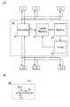
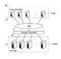
図1(A)には、本発明の一態様であるストレージシステムのブロック図を示す。図1には、ホスト11、ストレージ制御回路12、及びストレージ13を図示している。ストレージ制御回路12は、コントローラ21(図中、Controller と図示)、キャッシュメモリ22(図中、Cache Memory と図示)、蓄電装置23(図中、Battery と図示)及びタイマー24(図中、Timer と図示)を有する。<Regarding the block diagram of the storage system>
FIG. 1A is a block diagram of a storage system which is one embodiment of the present invention. FIG. 1 illustrates the
ホスト11は、ストレージ13に記憶されたデータにアクセスするコンピュータに相当する。ホスト11は、サーバという場合もある。ホスト11同士は、ネットワークで互いに接続されていてもよい。ホスト11からストレージ13へのアクセスによって入出力されるデータは、ストレージ制御回路12を介して行われる。ストレージ13からホスト11へのデータの入出力は、ストレージ制御回路12を介して行われる。The
ストレージ13は、ホスト11から出力されたデータを記憶する。またストレージ13は、ホスト11のアクセスによって必要なデータを出力する。ストレージ13は、ネットワークで互いに接続されていてもよい。ストレージ13は、大容量のデータを記憶することが求められる。ストレージ13は、ハードディスクドライブ(HDD)、あるいはフラッシュメモリを用いることができる。特にフラッシュメモリは、静音性、耐衝撃性に優れ、HDDよりもアクセススピードに優れている点で、好ましい。The
ストレージ13は、フラッシュメモリとすることでデータのアクセススピード、つまりデータの記憶及び出力に要する時間を短くしているものの、DRAMに比べて格段に長い。ストレージシステムでは、ストレージ13のアクセススピードの長さの問題を解決するために、通常キャッシュメモリを設けてデータの記憶及び出力を短くしている。キャッシュメモリは、アクセススピードの短いDRAMが設けられる。Although the
図1(A)においても、ストレージ制御回路12内にキャッシュメモリ22を有する。ホスト11とストレージ13との間でやり取りされるデータは、コントローラ21の制御によってキャッシュメモリに記憶されたのち、ホスト11またはストレージ13に出力される。Also in FIG. 1A, the
キャッシュメモリ22でデータを記憶するためのメモリセルには、データの記憶容量が大きいDRAMが用いられる。DRAMは、上述したようにアクセススピードにも優れており好ましい。しかしながら、DRAMは1秒間に数十回以上のデータのリフレッシュを必要とするため、消費電力が大きい。A DRAM having a large data storage capacity is used as a memory cell for storing data in the
DRAMは、一つのトランジスタと一つのキャパシタで構成される(1T1C)回路である。トランジスタには、チャネル形成領域にシリコンを有するトランジスタ(Siトランジスタ)が用いられる。Siトランジスタは、オフにした際のリーク電流(オフ電流)が大きいため、上述のリフレッシュを行う頻度が多くなる。The DRAM is a (1T1C) circuit including one transistor and one capacitor. As the transistor, a transistor including silicon in a channel formation region (Si transistor) is used. Since the Si transistor has a large leak current (OFF current) when it is turned off, the frequency of the above-described refresh increases.
またDRAMでは、電力の供給が停止する場合、データに応じた電位が維持できず、データが消えてしまう。そのため、スーパーキャパシタを設けて、一時的に電力の供給が停止しても、データをキャッシュメモリからストレージに退避するための電力を確保する構成があり得る。しかし、スーパーキャパシタは充電に時間を要するといった問題が残る。Further, in the DRAM, when the power supply is stopped, the potential corresponding to the data cannot be maintained and the data disappears. Therefore, there may be a configuration in which a supercapacitor is provided to secure the power for saving data from the cache memory to the storage even if the power supply is temporarily stopped. However, the problem that the supercapacitor takes time to charge remains.
本発明の一態様の構成では、キャッシュメモリのデータを記憶するためのトランジスタとして、オフ電流が小さいトランジスタを用いる。具体的には、チャネル形成領域に酸化物半導体を有するトランジスタ(OSトランジスタ)を用いる。OSトランジスタを用いてデータに応じた電位を保持する構成とすることで、リフレッシュする頻度を減らし、消費電力を小さくすることができる。タイマー24は定期的にデータをリフレッシュするタイミングを制御する信号を生成する。例えば一時間ごとに1回パルス信号を出力し、キャッシュメモリ22でリフレッシュを行うよう制御する。In the structure of one embodiment of the present invention, a transistor with low off-state current is used as a transistor for storing data in the cache memory. Specifically, a transistor including an oxide semiconductor in a channel formation region (OS transistor) is used. With the structure in which the potential corresponding to data is held using the OS transistor, the frequency of refreshing can be reduced and power consumption can be reduced. The
また本発明の一態様の構成で、キャッシュメモリ22を有するストレージ制御回路12は、蓄電装置23およびタイマー24を有する。ストレージシステムでは、一時的に電力の供給が停止した場合に、蓄電装置23からキャッシュメモリ22及びタイマー24に電力を供給する。そのため、ストレージ制御回路12の外部からの電力の供給がある場合、蓄電装置23の電力を消費することがない。Further, in the structure of one embodiment of the present invention, the
なお蓄電装置23は、リチウムイオン電池等の二次電池が好ましい。二次電池は、充放電が可能であり、小型化も容易であるため好適である。また、スーパーキャパシタ等とは異なり、放電後にその都度充電することが不要であるため、充電に要する時間を予め設ける必要がない。The
キャッシュメモリ22において、リフレッシュする頻度は、OSトランジスタを用いることで1時間に1回程度の頻度とすることができる。そのため、データをリフレッシュする頻度はDRAMに比べて少ない。従ってリフレッシュするために要する電力は小さくて済むため、蓄電装置23の小型化を図ることができる。なお蓄電装置23の電力は、タイマー24も必要とするが、タイマー24が消費する電力は小さく、小型の蓄電装置23としても問題ない。In the
例えば、蓄電装置23に一次電池、具体的には小型のボタン電池を採用し、電力の供給をすることも可能である。蓄電装置23は、一時間に一回程度といったデータのリフレッシュによる電力消費、及びタイマー24の動作による電力消費を行うことができる電力を供給できればよい。For example, a primary battery, specifically a small button battery, may be adopted as the
なお定期的なリフレッシュを行うことでキャッシュメモリ22にデータを半永久的に保持し続けることができる。この際のリフレッシュの頻度は上述したように非常に少ない。そのため、少ない消費電力でデータを保持し続けることができる。Data can be retained in the
なおキャッシュメモリ22が有するメモリセルの構成は、OSトランジスタを用いてデータに応じた電位を保持できる回路構成であればよい。例えば、DRAMが有するSiトランジスタをOSトランジスタに置き換えた構成とすることができる。Note that the memory cell included in the
図1(B)には、キャッシュメモリ22が有するメモリセル25の回路構成の一例を示す。メモリセル25は、トランジスタMTと、キャパシタCpと、を有する。トランジスタMTは、OSトランジスタを採用することで、ソースとドレインとの間を流れるオフ電流(図中、Ioff)を極めて小さい値にすることができる。そのため、トランジスタMTのゲートに与える信号SGによってトランジスタMTをオフにし続けることで、トランジスタMTとキャパシタCpのノードFNの電荷を保持し続け、データに応じた電位を保持することができる。図1(B)の回路構成は、Siトランジスタを有するDRAMの回路構成と同じであり、データの読み出し及び書き込みのアクセススピードが速いといった利点を有する。FIG. 1B shows an example of a circuit configuration of the
なお図1(B)では、トランジスタとキャパシタを用いてデータに応じた電位を保持するメモリセルの構成を例示的に示したが他の構成でもよい。例えば、OSトランジスタのソース又はドレインの一方と、Siトランジスタのゲートを接続したノードに電荷を保持し、データを保持する構成としてもよい。または、SRAMをベースとした回路構成に、OSトランジスタとキャパシタを追加し、データを退避させてデータを保持する構成としてもよい。Note that FIG. 1B exemplifies a structure of a memory cell in which a transistor and a capacitor are used to hold a potential corresponding to data, but another structure may be used. For example, a structure in which one of the source and the drain of the OS transistor and the gate of the Si transistor are connected to each other to hold electric charge and hold data may be employed. Alternatively, an OS transistor and a capacitor may be added to the circuit configuration based on the SRAM, and data may be saved to retain the data.
<ストレージシステムの動作について>
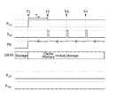
次いで、図1(A)に示したストレージシステムの動作について説明する。ここで図2には動作を説明するために、ストレージシステムの各構成から出力される信号、電力等を模式的に示す。また、図2には、外部からの電力の供給を行う電源26(Power Supplyと図示)を示している。<Operation of storage system>
Next, the operation of the storage system shown in FIG. 1A will be described. Here, in FIG. 2, in order to explain the operation, signals, electric power, etc. output from the respective components of the storage system are schematically shown. Further, FIG. 2 shows a power supply 26 (illustrated as Power Supply) that supplies electric power from the outside.
なお電源26は、蓄電装置23以外の電源のことをいう。例えば商用電源を電源26としてもよい。あるいはストレージシステムに併設された発電機、あるいは蓄電装置23とは別の蓄電装置を電源26としてもよい。なお電源26から供給される電圧は、コンバータ等を介して適切な電圧に変換して供給されることが好ましい。The
図2には、ストレージ13とキャッシュメモリ22との間で入出力されるデータDATAを図示している。また図2では、ホスト11とキャッシュメモリ22との間で入出力されるDATAを図示している。なお図2には、キャッシュメモリ22に入出力されるデータは、コントローラ21を介して行われるように図示している。FIG. 2 shows data DATA input/output between the
また図2では、電源26からストレージ制御回路12に供給される電力をPorgとして示している。また図2では、蓄電装置23からキャッシュメモリ22に供給される電力をPCMとして示している。また図2では、蓄電装置23からタイマー24に供給される電力をPTimとして示している。また図2では、タイマー24からキャッシュメモリ22に供給されるリフレッシュするタイミングを制御する信号をSrefとして示している。Further, in FIG. 2, the power supplied from the
まず電源26からストレージ制御回路12に電力が供給される場合のストレージシステムの動作について、図3にタイミングチャートを示し、説明する。なおタイミングチャートで示す信号及び電力は図2で図示したものである。なお、FNは、図1(B)で説明したノードFNの電位を表しており、図3ではハイレベルを維持することでデータに応じた電位を保持することを表している。First, the operation of the storage system when power is supplied from the
図3のタイミングチャートにおいて時刻T1では、電源26からの電力が供給される。図3では、Porgがハイレベルになることで電力の供給が行われることを表している。そしてストレージ13にあったデータDATAがキャッシュメモリ22に保持され、ホスト11からのアクセスに従ってストレージ13とキャッシュメモリ22の間、あるいはホスト11とキャッシュメモリ22との間で、それぞれ入出力される。ノードFNはデータに応じた電位が保持されたことを表すハイレベルとなる。なお蓄電装置23からキャッシュメモリ22に供給される電力、及び蓄電装置23からタイマー24に供給される電力は、電源26からの電力があるため、消費されない。そのためPCM、PTimをローレベルとし、電力の供給が行われないことを表している。In the timing chart of FIG. 3, power is supplied from the
一定期間、ホスト11とキャッシュメモリ22間、あるいはストレージ13とキャッシュメモリ22間でアクセスがないと、ノードFNの電位が低下する場合がある。そのため、タイマー24は電源26からストレージ制御回路12に供給される電力を利用して、リフレッシュ信号Srefを出力し、時刻T2乃至T4のように定期的にリフレッシュを行うことで、データの半永久的な保持を可能とすることができる。なおリフレッシュするか否かの判断は、タイマー24を用いて期間Tmの長さを測定し、リフレッシュを行う期間、例えば1時間に1回のリフレッシュであれば、Trefreshを1時間に設定し、TmがTrefreshを超えた時点でリフレッシュを行うように制御すればよい。If there is no access between the
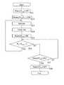
図3で説明したストレージシステムの一連の動作について、図4に示すフローチャートを用いて説明する。A series of operations of the storage system described in FIG. 3 will be described using the flowchart shown in FIG.
まずステップS01では、電源26からストレージ制御回路12への電力の供給を開始する(Power(Porg) ON)。First, in step S01, supply of electric power from the
次いでステップS02では、ホスト11とキャッシュメモリ22間、あるいはストレージ13とキャッシュメモリ22間のデータのアクセスが開始する(DATA Acccess)。Next, in step S02, access to data between the
次いでステップS03では、ノードFNにデータDATAを書き込んでからの期間Tmがリフレッシュする周期に相当するTrefreshを超えたか否かの判断を行う(Tm>Trefresh?)。TmがTrefreshを超えた場合、ステップS04でリフレッシュを行う(Refresh)。TmがTrefreshを超えない場合、ステップS05の判断を行う。Next, in step S03, it is determined whether or not the period Tm from writing the data DATA to the node FN exceeds Trefresh corresponding to therefresh cycle (Tm >Trefresh ?). If Tm exceeds Trefresh , refresh is performed in step S04 (Refresh). When Tm does not exceed Trefresh , the determination in step S05 is performed.
次いでステップS05では、ストレージシステムをシャットダウンするか否かの判断を行う(System Off?)。シャットダウンしない場合は、再度ステップS02を行う。シャットダウンする場合は、キャッシュメモリ22からストレージ13へのデータDATAの退避(転送)をする等を行い、終了する。Next, in step S05, it is determined whether or not to shut down the storage system (System Off?). If it is not shut down, step S02 is performed again. When shutting down, the data DATA is saved (transferred) from the
次いで、電源26からストレージ制御回路12への電力の供給が停止し、その後復帰する場合のストレージシステムの動作について、図5にタイミングチャートを示し、説明する。なおタイミングチャートで示す信号及び電力は図2で図示したものである。なお、FNは、図1(B)で説明したノードFNの電位を表しており、図5ではハイレベルを維持することでデータに応じた電位を保持することを表している。Next, the operation of the storage system when the supply of power from the
図5のタイミングチャートにおいて時刻T6では、電源26からストレージ制御回路12への電力の供給が停止する。図5では、Porgがハイレベルからローレベルになることで電力の供給が停止することを表している。ホスト11とキャッシュメモリ22間、あるいはストレージ13とキャッシュメモリ22間のデータのアクセスは停止し、データDATAはキャッシュメモリ22に保持される。なおデータDATAは、キャッシュメモリ22からストレージ13へのデータDATAの退避(転送)し、バックアップさせてもよい。At time T6 in the timing chart of FIG. 5, the power supply from the
ノードFNは、データに応じた電位が保持されているものの時間の経過とともに電位が低下する。そのため、蓄電装置23は、電力の供給が停止するとともにPCM、PTimをハイレベルとする。そしてデータDATAのリフレッシュと、タイマー24による期間Tmのカウントを開始する。キャッシュメモリ22におけるデータDATAのリフレッシュは、間欠的に行われるため、リフレッシュが完了した後、PCMはローレベルとする。この間欠的なリフレッシュとタイマーの動作は、頻繁に行うリフレッシュの動作と比べて、消費電力が小さい。Although the potential of the node FN is held according to the data, the potential of the node FN decreases with the passage of time. Therefore, the
一定期間、データDATAのリフレッシュがないと、ノードFNの電位が低下する場合がある。そのため、タイマー24は蓄電装置23の電力PTimによって期間Tmを計測し、定期的にリフレッシュが行なわれるようリフレッシュ信号Srefを出力する。図5では、時刻T7、時刻T8のように定期的にリフレッシュを行うことで、データの半永久的な保持を可能とすることができる。リフレッシュを行う場合定期的に電力PCMを消費する。If the data DATA is not refreshed for a certain period, the potential of the node FN may decrease. Therefore, the
また図5のタイミングチャートにおいては、電力の供給を停止している状態から復帰する動作を説明する。この場合、Porgがハイレベルに立ちあがる(時刻T9)。Porgがハイレベルとなることで、PCM、PTimをローレベルとする。そして時刻T10でリフレッシュをした上で、ホスト11とキャッシュメモリ22間、あるいはストレージ13とキャッシュメモリ22間のデータのアクセスを再開すればよい。In the timing chart of FIG. 5, the operation of returning from the state where the power supply is stopped will be described. In this case, Porg rises to the high level (time T9). When Porg becomes high level, PCM and PTim become low level. Then, after refreshing at time T10, access to data between the
図5で説明した、電力の供給を停止している状態とし、その後復帰する場合のストレージシステムの一連の動作について、図6に示すフローチャートを用いて説明する。A series of operations of the storage system described in FIG. 5 when the power supply is stopped and then restored will be described with reference to the flowchart shown in FIG.
まずステップS11では、電力の供給を停止する(Power(Porg) OFF)。First, in step S11, power supply is stopped (Power(Porg )OFF).
次いでステップS12では、蓄電装置23によるキャッシュメモリ22およびタイマー24への電力の供給を開始する(Power(PCM、PTim) ON)。Next, in step S12, power supply from the
次いでステップS13では、データDATAのリフレッシュを行う(Refresh)。このリフレッシュは、蓄電装置23から供給される電力PCMによって行われる。Next, in step S13, the data DATA is refreshed (Refresh). This refresh is performed by the electric power PCM supplied from the
次いでステップS14では、タイマー24による期間Tmの測定を開始する(Timer Set)。なおステップS12、S13、S14は、同時に行われてもよい。Next, in step S14, the measurement of the period Tm by the
次いでステップS15では、ステップS13でリフレッシュが行われたため、蓄電装置23から供給される電力PCMを停止する。(Power(PCM) OFF)。Next, in step S15, since the refresh is performed in step S13, the power PCM supplied from the
次いでステップS16では、ノードFNのデータDATAをリフレッシュしてからの期間Tmがリフレッシュする周期に相当するTrefreshを超えたか否かの判断を行う(Tm>Trefresh?)。TmがTrefreshを超えた場合、ステップS13でリフレッシュを行う(Refresh)。TmがTrefreshを超えない場合、ステップS17の判断を行う。Next, in step S16, it is determined whether or not the period Tm after refreshing the data DATA of the node FN exceeds Trefresh corresponding to therefresh cycle (Tm >Trefresh ?). If Tm exceeds Trefresh , refresh is performed in step S13 (Refresh). When Tm does not exceed Trefresh , the determination in step S17 is performed.
次いでステップS17では、電源26からのストレージシステムへの電力の供給を復帰するか否かの判断を行う(Power(Porg) ON?)。復帰しない場合は、再度ステップS16を行う。復帰する場合は、ステップS18を行う。Next, in step S17, it is determined whether or not the power supply from the
次いでステップS18では、蓄電装置23から供給される電力PTimを停止する。(Power(PTim) OFF)。
<まとめ>
以上説明したように、本実施の形態の構成のストレージシステムは、電力の供給を停止してもデータの保持が可能なストレージシステムとすることができる。またデータの保持に要する電力を削減することができる。本実施の形態の構成のストレージシステムでは、オフ電流の小さいトランジスタを有するメモリセルを用いる。オフ電流が小さいことを利用してデータの保持を図るとともに、1時間に1回程度のリフレッシュを行うことでデータの半永久的な保持を実現することができる。また電力の供給を停止する期間においては、トランジスタをオフにし続けることができる電力を用いて、データの保持を図ることで、データの退避を行う構成に比べて大幅に電力を削減することができる。Next, in step S18, the electric power PTim supplied from the
<Summary>
As described above, the storage system having the configuration of this embodiment can be a storage system that can retain data even when power supply is stopped. In addition, the power required for holding data can be reduced. In the storage system having the structure of this embodiment mode, a memory cell including a transistor whose off-state current is small is used. Data can be held by utilizing the fact that the off-state current is small, and semi-permanent holding of data can be realized by performing refreshing about once per hour. Further, in the period in which the power supply is stopped, power can be retained by using power that can continue to turn off the transistor, so that power can be significantly reduced compared to a structure in which data is saved. ..
(実施の形態2)
本実施の形態では、上記実施の形態1で説明したキャッシュメモリが有するメモリセルに適用可能な回路構成の一例について説明する。(Embodiment 2)
In this embodiment, an example of a circuit structure which can be applied to the memory cell included in the cache memory described in
<OSトランジスタとキャパシタを組み合わせた回路構成>
図7(A)の回路図に示すメモリセルMCは、トランジスタM1と、キャパシタC1を有する。トランジスタM1は、例えばオフ電流の極めて小さいOSトランジスタで構成する。メモリセルMCは、ビット線BL、ワード線WLによって動作する。なおメモリセルMCは、例えばマトリクス状に複数設けられる。<Circuit configuration combining OS transistor and capacitor>
The memory cell MC shown in the circuit diagram of FIG. 7A includes a transistor M1 and a capacitor C1. The transistor M1 is, for example, an OS transistor whose off-state current is extremely low. The memory cell MC operates by the bit line BL and the word line WL. A plurality of memory cells MC are provided in a matrix, for example.
メモリセルMCの書き込み動作、および読み出し動作は、基本的にDRAM(Dynamic Random Access Memory)と同じである。すなわち、ワード線WLで選択したメモリセルMCにビット線BLに与えてデータを書きこむ。また、ワード線WLで選択したメモリセルMCからビット線BLにデータを読み出す。The write operation and the read operation of the memory cell MC are basically the same as those of a DRAM (Dynamic Random Access Memory). That is, the data is written by giving it to the bit line BL to the memory cell MC selected by the word line WL. In addition, data is read from the memory cell MC selected by the word line WL to the bit line BL.
トランジスタM1は、上記したようにオフ電流が極めて小さい。そのためトランジスタM1をオフにすることで、一度キャパシタC1に保持したデータに対応する電荷を保持し続けることができる。従って、Siトランジスタを有するDRAMのメモリセルと異なり、リフレッシュする間隔を長くすることができる。その結果、半導体装置の低消費電力化を図ることができる。The off-state current of the transistor M1 is extremely small as described above. Therefore, by turning off the transistor M1, electric charge corresponding to the data once held in the capacitor C1 can be kept held. Therefore, unlike the memory cell of the DRAM having the Si transistor, the refresh interval can be extended. As a result, low power consumption of the semiconductor device can be achieved.
次に、メモリセルMCの周辺回路の構成を図7(B)に示す。Next, a structure of a peripheral circuit of the memory cell MC is shown in FIG.
図7(B)には、メモリセルMCの周辺回路として、プリチャージ回路Cpre、センスアンプSA、スイッチSWを図示している。また図7(B)には、ビット線BL_1に接続されたメモリセルMC_1、ビット線BL_2に接続されたメモリセルMC_2と、を図示している。ビット線BL_1及びビット線BL_2は、図7(A)のビット線BLに相当する。また、メモリセルMC_1およびメモリセルMC_2は、図7(A)のメモリセルMCに相当する。FIG. 7B shows a precharge circuit Cpre, a sense amplifier SA, and a switch SW as peripheral circuits of the memory cell MC. In addition, FIG. 7B illustrates a memory cell MC_1 connected to the bit line BL_1 and a memory cell MC_2 connected to the bit line BL_2. The bit line BL_1 and the bit line BL_2 correspond to the bit line BL in FIG. 7A. The memory cell MC_1 and the memory cell MC_2 correspond to the memory cell MC in FIG. 7A.
プリチャージ回路Cpreは複数のトランジスタM2を有する。プリチャージ回路Cpreは、ビット線BL_1、BL_2をプリチャージ電位Vpreにプリチャージし、互いに均等な電位にする。プリチャージ回路Cpreは、プリチャージ信号Spreによって制御される。The precharge circuit Cpre has a plurality of transistors M2. The precharge circuit Cpre precharges the bit lines BL_1 and BL_2 to the precharge potential Vpre to make them equal potentials. The precharge circuit Cpre is controlled by the precharge signal Spre.
センスアンプSAは複数のトランジスタM3を有する。センスアンプSAは、ビット線BL_1、BL_2間の電位差を増幅する。センスアンプSAは、電位SP、SNによって、ビット線BL_1、BL_2の電位差を増幅する。The sense amplifier SA has a plurality of transistors M3. The sense amplifier SA amplifies the potential difference between the bit lines BL_1 and BL_2. The sense amplifier SA amplifies the potential difference between the bit lines BL_1 and BL_2 by the potentials SP and SN.
スイッチSWは複数のトランジスタM4を有する。スイッチSWは、信号CSELの制御に従って、センスアンプSAで増幅されたビット線BL_1、BL_2の電位差を、データDout、Dout_bとして読み出し回路に出力する。The switch SW has a plurality of transistors M4. The switch SW outputs the potential difference between the bit lines BL_1 and BL_2 amplified by the sense amplifier SA to the read circuit as data Dout and Dout_b under the control of the signal CSEL.
トランジスタM2、M3、およびM4は、Siトランジスタで構成される。Siトランジスタは、OSトランジスタに比べて電界効果移動度が大きい。そのためプリチャージ回路Cpre、センスアンプSA、スイッチSWの各回路は、良好なスイッチング特性を有せしめることができる。The transistors M2, M3, and M4 are Si transistors. The Si transistor has a larger field effect mobility than the OS transistor. Therefore, each circuit of the precharge circuit Cpre, the sense amplifier SA, and the switch SW can have good switching characteristics.
<OSトランジスタと、Siトランジスタを組み合わせた回路構成>
図8(A)の回路図に示すメモリセルMC_Cは、トランジスタM5と、キャパシタC2と、トランジスタM6を有する。トランジスタM5は、例えばオフ電流の極めて小さいOSトランジスタで構成する。トランジスタM6は、チャネル形成領域にシリコンを有するトランジスタ(Siトランジスタ)で構成する。メモリセルMC_Cは、ビット線BL、書き込みワード線WWL、読み出しワード線RWL、ソース線SLによって動作する。なおメモリセルMC_Cは、例えばマトリクス状に複数設けられる。<Circuit configuration combining OS transistor and Si transistor>
The memory cell MC_C illustrated in the circuit diagram of FIG. 8A includes a transistor M5, a capacitor C2, and a transistor M6. The transistor M5 is formed of, for example, an OS transistor with extremely low off-state current. The transistor M6 is a transistor (Si transistor) having silicon in the channel formation region. The memory cell MC_C operates by the bit line BL, the write word line WWL, the read word line RWL, and the source line SL. Note that the memory cells MC_C are provided in a matrix, for example.
メモリセルMC_Cの書き込み動作は、書き込みワード線WWLを制御して、トランジスタM5を導通状態にする。そしてビット線BLに与えられたデータを、ノードFNに与える。ノードFNに与えたデータに応じた電荷を保持するため、書き込みワード線WWLを制御して、トランジスタM5を非導通状態にする。In the write operation of the memory cell MC_C, the write word line WWL is controlled to make the transistor M5 conductive. Then, the data given to the bit line BL is given to the node FN. In order to retain the charge according to the data given to the node FN, the write word line WWL is controlled so that the transistor M5 is turned off.
メモリセルMC_Cの読み出し動作は、トランジスタM5を非導通状態として、読み出しワード線RWLを制御して行う。ノードFNは、電気的に浮遊状態のため、読み出しワード線RWLの変化に従って、電位が変化する。この変化によって、ノードFNに与えたデータに応じて、トランジスタM6の導通状態を異ならせることができる。このトランジスタM6の導通状態の変化に応じてビット線BLとソース線との間に電流が流れてビット線BLの電位が変化し、データを読み出すことができる。The read operation of the memory cell MC_C is performed by setting the transistor M5 in a non-conducting state and controlling the read word line RWL. Since the node FN is in an electrically floating state, the potential changes as the read word line RWL changes. Due to this change, the conduction state of the transistor M6 can be changed according to the data applied to the node FN. According to the change in the conduction state of the transistor M6, a current flows between the bit line BL and the source line, the potential of the bit line BL changes, and data can be read.
トランジスタM5は、上記したようにオフ電流が極めて小さい。そのためトランジスタM5をオフにすることで、一度キャパシタC2に保持したデータに対応する電荷を保持し続けることができる。また、メモリセルMC_Cは、Siトランジスタを有するDRAMのメモリセルと異なり、データを読み出しても、元のデータは維持される。従って、トランジスタM5を非導通状態に維持することで、不揮発性のメモリセルとして機能させることができる。The off-state current of the transistor M5 is extremely small as described above. Therefore, by turning off the transistor M5, the electric charge corresponding to the data once held in the capacitor C2 can be kept held. Further, the memory cell MC_C is different from the memory cell of the DRAM having the Si transistor in that the original data is maintained even when the data is read. Therefore, by maintaining the transistor M5 in a non-conducting state, it can function as a nonvolatile memory cell.
トランジスタM6は、Siトランジスタで構成される。Siトランジスタは、OSトランジスタに比べて電界効果移動度が大きい。そのためノードFNの電位に応じてビット線BL、ソース線SL間に流れる電流量を増やすことができ、データの読み出し動作におけるビット線の電位の変動を高速で行うことができる。The transistor M6 is composed of a Si transistor. The Si transistor has a larger field effect mobility than the OS transistor. Therefore, the amount of current flowing between the bit line BL and the source line SL can be increased according to the potential of the node FN, and the potential of the bit line in the data reading operation can be changed at high speed.
次いで、図8(A)で示したメモリセルMC_Cとは異なる回路構成について説明する。Next, a circuit structure different from that of the memory cell MC_C illustrated in FIG. 8A will be described.
図8(A)に示すメモリセルMC_Cは、トランジスタM6をpチャネル型のトランジスタとしたが、他の構成でもよい。例えば、図8(B)に示すメモリセルMC_Dのように、nチャネル型のトランジスタとしたトランジスタM6_Aを有する構成としてもよい。In the memory cell MC_C illustrated in FIG. 8A, the transistor M6 is a p-channel transistor, but another structure may be used. For example, the memory cell MC_D illustrated in FIG. 8B may have a structure including the transistor M6_A which is an n-channel transistor.
図8(A)に示すメモリセルMC_Cは、トランジスタM5を書き込みワード線WWLに接続されたトランジスタとしたが、他の構成でもよい。例えば、図8(C)に示すメモリセルMC_Eのように、バックゲートを追加したトランジスタM5_BGとし、バックゲートに配線BGLより電位を与える構成としてもよい。これにより、トランジスタM5_BGの閾値電圧の制御可能な構成とすることができる。In the memory cell MC_C illustrated in FIG. 8A, the transistor M5 is a transistor connected to the write word line WWL, but another structure may be used. For example, like the memory cell MC_E illustrated in FIG. 8C, the transistor M5_BG with an additional back gate may be used and a potential may be applied to the back gate from the wiring BGL. Accordingly, the threshold voltage of the transistor M5_BG can be controlled.
図8(A)に示すメモリセルMC_Cは、ビット線BL、ソース線SL間の電流の流れをトランジスタM6で制御する構成としたが、他の構成でもよい。例えば、図8(D)に示すメモリセルMC_Fのように、ビット線BL、ソース線SL間に、トランジスタM6_B、およびトランジスタM6_Cの複数のトランジスタを設ける構成としてもよい。これにより、ノードFNの電位をキャパシタC2の容量結合によって調整する動作を行うことなく、ビット線BL、ソース線SL間の電流の流れを制御することができる。Although the memory cell MC_C illustrated in FIG. 8A has a structure in which the transistor M6 controls the current flow between the bit line BL and the source line SL, another structure may be used. For example, as in the memory cell MC_F illustrated in FIG. 8D, a plurality of transistors M6_B and M6_C may be provided between the bit line BL and the source line SL. As a result, the flow of current between the bit line BL and the source line SL can be controlled without performing the operation of adjusting the potential of the node FN by the capacitive coupling of the capacitor C2.
なお図8(D)では、トランジスタM6_B、およびトランジスタM6_Cをnチャネル型のトランジスタとしたが、他の構成でもよい。例えば、図8(E)に示すメモリセルMC_Gのように、ビット線BL、ソース線SL間に設ける、トランジスタM6_D、およびトランジスタM6_Eをpチャネル型のトランジスタとしてもよい。Note that although the transistor M6_B and the transistor M6_C are n-channel transistors in FIG. 8D, other structures may be used. For example, like the memory cell MC_G illustrated in FIG. 8E, the transistor M6_D and the transistor M6_E provided between the bit line BL and the source line SL may be p-channel transistors.
図8(A)に示すメモリセルMC_Cは、データを書きこむ動作と、データを読み出す動作で、同じビット線BLを利用して行う構成を示したが、他の構成でもよい。例えば、図8(F)に示すメモリセルMC_Hのように、データを書きこむためのビット線WBL、データを読み出すためのビット線RBLを設ける構成としてもよい。Although the memory cell MC_C illustrated in FIG. 8A has a structure in which the same bit line BL is used for the data writing operation and the data reading operation, another structure may be used. For example, as in the memory cell MC_H illustrated in FIG. 8F, a bit line WBL for writing data and a bit line RBL for reading data may be provided.
次いで、図8(A)で示したメモリセルMC_C(以下、メモリセルMCともいう)を動作させるための駆動回路を含むブロック図の一例を図9に示す。なお図9では、メモリセルがm行n列(m、nは2以上の自然数)に設けられるものとし、(m−1)行目、m行目の(n−1)列目、n列目を図示している。Next, FIG. 9 illustrates an example of a block diagram including a driver circuit for operating the memory cell MC_C illustrated in FIG. 8A (hereinafter also referred to as a memory cell MC). Note that in FIG. 9, memory cells are provided in m rows and n columns (m and n are natural numbers of 2 or more), and the (m−1)th row, the mth row, the (n−1)th column, and the nth column. The eye is illustrated.
図9のブロック図では、m行n列に設けたメモリセルMC(図中、MC[m、n])、が複数設けられたメモリセルアレイ101、行選択ドライバ102、および列選択ドライバ103、を示している。また図9では、書き込みワード線WWL、読み出しワード線RWL、ビット線BL、ソース線SLとして、書き込みワード線WWL[m−1]、読み出しワード線RWL[m−1]、書き込みワード線WWL[m]、読み出しワード線RWL[m]、ビット線BL[n−1]、ビット線BL[n]、ソース線SL[n−1]、およびソース線SL[n]を示している。In the block diagram of FIG. 9, a
行選択ドライバ102は、各行におけるメモリセルMCを選択するための信号を出力する回路である。列選択ドライバ103は、メモリセルMCへのデータ電圧の書き込み、メモリセルMCからのデータ電圧の読み出し、を行うための信号を出力する回路である。行選択ドライバ102および列選択ドライバ103はデコーダ等の回路を有し、各行、各列に信号またはデータ電圧を出力することができる。The
<SRAMをベースにOSトランジスタを組み合わせた回路構成>
図10(A)に示すメモリセルMC_Iは、SRAM、トランジスタM7、キャパシタC3、を有する。SRAMは、トランジスタM8、インバータ回路INVを有する。メモリセルMC_Iは、配線WWLに与える信号の制御によって、SRAMのノードQ,QBのデータをノードFN1、FN2にバックアップし、ノードFN1、FN2からノードQ,QBへのデータのリカバリーを制御する。トランジスタM7を非導通状態にすることで、ノードFN1、FN2にデータに応じた電荷を保持することができる。<Circuit configuration combining OS transistors based on SRAM>
The memory cell MC_I illustrated in FIG. 10A includes an SRAM, a transistor M7, and a capacitor C3. The SRAM has a transistor M8 and an inverter circuit INV. The memory cell MC_I backs up the data of the nodes Q and QB of the SRAM to the nodes FN1 and FN2 and controls the recovery of the data from the nodes FN1 and FN2 to the nodes Q and QB by controlling the signal applied to the wiring WWL. By turning off the transistor M7, electric charge corresponding to data can be held in the nodes FN1 and FN2.
また図10(B)に示すメモリセルMC_Jは、SRAM、トランジスタM9、インバータ回路INV、キャパシタC4、およびトランジスタM10、を有する。メモリセルMC_Jは、配線WWL、配線RENに与える信号の制御によって、SRAMのノードQまたはQBのデータをノードFN3にバックアップし、ノードFN3からノードQまたはQBへのデータのリカバリーを制御する。トランジスタM9を非導通状態にすることで、ノードFN3にデータに応じた電荷を保持することができる。The memory cell MC_J illustrated in FIG. 10B includes an SRAM, a transistor M9, an inverter circuit INV, a capacitor C4, and a transistor M10. The memory cell MC_J backs up the data of the node Q or QB of the SRAM to the node FN3 and controls the recovery of the data from the node FN3 to the node Q or QB by controlling the signals given to the wiring WWL and the wiring REN. By turning off the transistor M9, charge corresponding to data can be held in the node FN3.
以上の説明したストレージシステムのキャッシュメモリのメモリセルには、上記実施の形態の構成を適用可能である。このため、低消費電力化が図られたストレージシステムが実現される。The configurations of the above-described embodiments can be applied to the memory cells of the cache memory of the storage system described above. Therefore, a storage system with low power consumption is realized.
(実施の形態3)
本実施の形態では、実施の形態2で説明したメモリセルが有するトランジスタの断面の構造について、図面を参照して説明する。本実施の形態ではトランジスタとして、Siトランジスタを有する層、およびOSトランジスタを有する層について説明する。また、OSトランジスタが有する酸化物半導体について詳述する。また、OSトランジスタを有する層とSiトランジスタを有する層とを重ねて設けた構成の一例について説明する。(Embodiment 3)
In this embodiment, a structure of a cross section of a transistor included in the memory cell described in
<Siトランジスタを有する層の断面構造について>
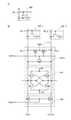
図11(A)は、Siトランジスタを有する層におけるトランジスタの一例を説明するための、上面図である。図11(A)には、トランジスタ200Aを示している。<Regarding Cross-sectional Structure of Layer Having Si Transistor>
FIG. 11A is a top view illustrating an example of a transistor in a layer including a Si transistor. A
図11(B)は、図11(A)に示すトランジスタ200Aの破線A1−A2で示す領域の断面模式図である。なお破線A1−A2で示す領域では、トランジスタ200Aのチャネル長方向における構造を示している。11B is a schematic cross-sectional view of a region of the
図11(C)は、図11(A)に示すトランジスタ200Aの破線A3−A4で示す領域の断面模式図である。なお破線A3−A4で示す領域では、トランジスタ200Aのチャネル幅方向における構造を示している。11C is a schematic cross-sectional view of a region of the
図11(A)では、トランジスタ200Aの半導体層202、およびゲート電極205のレイアウトを示している。半導体層202は、ゲート電極と重なる領域にチャネル形成領域、素子分離層に囲まれる領域に不純物領域が形成される層である。なお以下では、トランジスタ200Aを、pチャネル型のトランジスタであるとして説明する。FIG. 11A shows a layout of the
図11(B)では、基板201、不純物領域202A、202B、素子分離領域203、ゲート絶縁層204、ゲート電極205、および層間絶縁層206を図示している。In FIG. 11B, the
図11(C)では、基板201、素子分離領域203、ゲート絶縁層204、ゲート電極205、および層間絶縁層206を図示している。In FIG. 11C, the
基板201は、例えば、シリコン基板、ゲルマニウム基板、シリコンゲルマニウム基板等を用いることができる。図11(A)乃至(C)では、単結晶シリコン基板を基板200として用いる場合を例示している。なお基板201は、例えば、n型の導電型を付与する不純物を有する半導体基板を用いる。基板201として、p型の導電型を付与する不純物を有する半導体基板を用いてもよい。その場合、トランジスタ200Aとなる領域には、n型の導電型を付与する不純物を有するウェルを配置すればよい。As the
不純物領域202A、202Bは、ソース領域およびドレイン領域としての機能を有する。不純物領域202A、202Bは、例えばp型の導電型を付与する不純物を有する領域である。The
素子分離領域203は、隣接するトランジスタ間を電気的に分離するための領域である。素子分離領域203は、トレンチ分離法(STI法:Shallow Trench Isolation)等を用いて形成することができる。トレンチ分離法は、エッチング等により基板に形成されたトレンチに、酸化珪素などが含まれる絶縁物を埋め込んだ後、当該絶縁物をエッチング等により部分的に除去することで形成される素子分離領域により、トランジスタ間を素子分離させる方法である。The
また、ゲート絶縁層204は、熱酸化膜、酸化シリコン膜、窒化シリコン膜または酸化窒化シリコン膜などの単層または積層構造を用いることができる。The
ゲート電極205は、リンが添加された多結晶シリコンを用いることができる。多結晶シリコンの他に、金属とシリコンの化合物であるシリサイドでもよい。For the
層間絶縁層206は、比誘電率が低く、かつ十分な厚さを有すると好ましい。例えば、比誘電率が3.8程度である酸化シリコン膜を用いればよい。The interlayer insulating
また図11(A)乃至(C)で示した、Siトランジスタを有する層におけるトランジスタとは異なる構成を図12(A)乃至(C)に示す。図12(A)乃至(C)に示すトランジスタ200Bは、図11(A)乃至(C)に示すトランジスタ200AがFin型である場合を示している。トランジスタ200BをFin型とすることにより、実効的なチャネル幅が増大し、それによりトランジスタ200Bのオン特性を向上させることができる。また、ゲート電極の電界の寄与を高くすることができるため、トランジスタ200Bのオフ特性を向上させることができる。In addition, structures different from the transistor in the layer including the Si transistor illustrated in FIGS. 11A to 11C are illustrated in FIGS. A
また図11(A)乃至(C)、または図12(A)乃至(C)で示した、Siトランジスタを有する層におけるトランジスタとは異なる構成を図13(A)乃至(C)に示す。図13(A)乃至(C)に示すトランジスタ200Cは、SOI基板である基板207に設けられた場合を示している。図13(A)乃至(C)には、絶縁層208によって領域209が基板207と分離されている構造を示す。基板207としてSOI基板を用いることによって、パンチスルー現象などを抑制することができるためトランジスタ200Cのオフ特性を向上させることができる。なお、絶縁層208は、基板207を絶縁層化させることによって形成することができる。例えば、絶縁層208としては、酸化シリコンを用いることができる。13A to 13C show different structures from the transistor in the layer including the Si transistor shown in FIGS. 11A to 11C or 12A to 12C. A
<OSトランジスタを有する層の断面構造について>
次いで図14(A)は、OSトランジスタを有する層におけるトランジスタの一例を説明するための、上面図である。図14(A)には、トランジスタ300Aを示している。<Regarding Cross-sectional Structure of Layer Having OS Transistor>
Next, FIG. 14A is a top view for illustrating an example of a transistor in a layer including an OS transistor. A
図14(B)は、図14(A)に示すトランジスタ300Aの破線B1−B2で示す領域の断面模式図である。なお破線B1−B2で示す領域では、トランジスタ300Aのチャネル長方向における構造を示している。14B is a schematic cross-sectional view of a region of the
図14(C)は、図14(A)に示すトランジスタ300Aの破線B3−B4で示す領域の断面模式図である。なお破線B3−B4で示す領域では、トランジスタ300Aのチャネル幅方向における構造を示している。14C is a schematic cross-sectional view of a region indicated by dashed lines B3-B4 of the
図14(A)では、トランジスタ300Aの酸化物半導体層303、酸化物半導体層303に接する配線304A、304B、およびゲート電極306のレイアウトを示している。酸化物半導体層303は、2層の酸化物半導体層303A、303Bが重なった層である。また、ゲート電極306の下層には、酸化物半導体層303Cが重なって設けられている。酸化物半導体層303A乃至303Cは、金属元素の原子数比の異なる酸化物半導体である。なお酸化物半導体層303A及び酸化物半導体層303Cは、絶縁層としての機能を有する場合がある。そのため、酸化物半導体層303A及び酸化物半導体層303Cを、酸化物層、あるいは絶縁層という場合がある。In FIG. 14A, a layout of the
図14(B)では、層間絶縁層301、絶縁層302、酸化物半導体層303A乃至303C、配線304A、304B、ゲート絶縁層305、およびゲート電極306を図示している。In FIG. 14B, the
図14(C)では、層間絶縁層301、絶縁層302、酸化物半導体層303A乃至303C、ゲート絶縁層305、およびゲート電極306を図示している。In FIG. 14C, the
層間絶縁層301は、トランジスタ300Aより下層の絶縁層に接する層間絶縁層である。配線となる導電層が埋め込まれた構成でもよい。The interlayer insulating
絶縁層302は、酸素、水素、水の拡散を防ぐブロッキング効果を有する層である。絶縁層302は、密度が高くて緻密である程、また未結合手が少なく化学的に安定である程、より高いブロッキング効果を示す。酸素、水素、水の拡散を防ぐブロッキング効果を示す絶縁層302として、例えば、酸化アルミニウム、酸化窒化アルミニウム、酸化ガリウム、酸化窒化ガリウム、酸化イットリウム、酸化窒化イットリウム、酸化ハフニウム、酸化窒化ハフニウム等を用いることができる。水素、水の拡散を防ぐブロッキング効果を示す絶縁層302として、例えば、窒化シリコン、窒化酸化シリコン等を用いることができる。The insulating
酸化物半導体層303A乃至303Cは、構成する金属元素の原子数比が異なる酸化物半導体である。酸化物半導体については、後の実施の形態で詳述する。The
ゲート絶縁層305は、加熱により酸素の一部を酸化物半導体層303A乃至303Cに供給する機能を有する絶縁膜であることが望ましい。また、ゲート絶縁層305は、欠陥が少ないことが好ましく、代表的には、ESR測定により得られる、シリコンのダングリングボンドに由来するg=2.001を持つスピンの密度が1×10¹⁸spins/cm3以下であることが好ましい。The
ゲート絶縁層305は、加熱により上記酸素の一部を酸化物半導体層303A乃至303Cに供給する機能を有するため、酸化物であることが望ましく、例えば、酸化アルミニウム、酸化マグネシウム、酸化珪素、酸化窒化珪素、窒化酸化珪素、酸化ガリウム、酸化ゲルマニウム、酸化イットリウム、酸化ジルコニウム、酸化ランタン、酸化ネオジム、酸化ハフニウムおよび酸化タンタルなどを用いることができる。ゲート絶縁層305は、プラズマCVD(Chemical Vapor Deposition)法またはスパッタリング法等により、形成することができる。The
なお、本明細書中において、酸化窒化物は、その組成として、窒素よりも酸素の含有量が多い材料を指し、窒化酸化物は、その組成として、酸素よりも窒素の含有量が多い材料を指す。Note that in this specification, an oxynitride refers to a material whose content of oxygen is higher than that of nitrogen as its composition, and a nitride oxide refers to a material whose content of nitrogen is higher than that of oxygen as its composition. Point to.
ゲート電極306は、例えば、ホウ素、窒素、酸素、フッ素、シリコン、リン、アルミニウム、チタン、クロム、マンガン、コバルト、ニッケル、銅、亜鉛、ガリウム、イットリウム、ジルコニウム、モリブデン、ルテニウム、銀、インジウム、スズ、タンタル、白金、ストロンチウム、イリジウムおよびタングステンを一種以上含む導電体を、単層または積層で用いればよい。例えば、合金や化合物であってもよく、アルミニウムを含む導電体、銅およびチタンを含む導電体、銅およびマンガンを含む導電体、インジウム、スズおよび酸素を含む導電体、チタンおよび窒素を含む導電体などを用いてもよい。The
図14(A)乃至(C)に示すトランジスタ300Aのように、ゲート電極306の電界によって、酸化物半導体層303Bを電気的に取り囲むことができる(導電体から生じる電界によって、半導体を電気的に取り囲むトランジスタの構造を、surrounded channel(s−channel)構造とよぶ。)。そのため、酸化物半導体層303Bの全体(上面、および側面)にチャネルが形成される。s−channel構造では、トランジスタのソース−ドレイン間に大電流を流すことができ、導通時の電流(オン電流)を高くすることができる。As in the
なお図15(A)に示すトランジスタ300Dのように、層間絶縁層301と絶縁層302との間に、バックゲート電極307を設ける構成としてもよい。また図15(B)に示すトランジスタ300Eのように、ゲート絶縁層305および酸化物半導体層303Cがゲート電極306から迫り出した形状としてもよい。また図15(C)に示すトランジスタ300Fのように、ゲート絶縁層305および酸化物半導体層303Cで、酸化物半導体層303A、303B、配線304A、304Bを覆う形状としてもよい。(図15(C)参照。)。Note that as in the
また図16(A)に示すトランジスタ300Gのように、B1−B2断面における配線304A、304Bの端部が、酸化物半導体層303A、303Bと同じであってもよい。また図16(B)に示すトランジスタ300Hのように、ゲート電極306、ゲート絶縁層305および酸化物半導体層303Cが、配線304A、304Bと重なる領域が小さくなるようにしてもよい。図16(C)に示すトランジスタ300Iのように、ゲート絶縁層305および酸化物半導体層303Cで、酸化物半導体層303A、303B、配線304A、304Bの上面および側面を覆う形状としてもよい。Further, as in the
また、図17(A)乃至(C)に示すトランジスタ300Bのように、酸化物半導体層303Cを省略してもよい。図17(A)は上面図の一例である。図17(B)は、図17(A)に示すトランジスタ300Bの破線B1−B2で示す領域の断面模式図である。図17(C)は、図17(A)に示すトランジスタ300Bの破線B3−B4で示す領域の断面模式図である。Alternatively, the
<Siトランジスタを有する層とOSトランジスタを有する層とを積層した断面構造について>
次いで図18では、図11乃至図13で説明したSiトランジスタを有する層と、図14乃至図17で説明したOSトランジスタを有する層と、を積層した際の断面構造の一例について示す。<Regarding the cross-sectional structure in which a layer having a Si transistor and a layer having an OS transistor are stacked>
Next, FIG. 18 illustrates an example of a cross-sectional structure when the layer including the Si transistor described in FIGS. 11 to 13 and the layer including the OS transistor described in FIGS. 14 to 17 are stacked.
図18では、図11(A)に示すトランジスタ200Aと、図15(C)に示すトランジスタ300Fと、を積層した断面模式図の一例である。18 is an example of a schematic cross-sectional view in which the
図18に示す断面模式図では、配線401と、配線402と、絶縁層406と、絶縁層408と、絶縁層410と、絶縁層412と、絶縁層414と、絶縁層416と、絶縁層418と、絶縁層420と、絶縁層422と、絶縁層424と、絶縁層426と、絶縁層428と、絶縁層430と、絶縁層431と、絶縁層432と、絶縁層434と、絶縁層436と、絶縁層438と、絶縁層440と、絶縁層442と、絶縁層444と、絶縁層446と、配線451と、配線452と、配線461と、配線462と、配線463と、を示している。In the schematic cross-sectional view illustrated in FIG. 18, the
なおトランジスタ300Fは、絶縁層420および絶縁層422の開口部に設けられた配線をバックゲート電極307として有する。バックゲート電極を有することで、電気的な特性が安定したトランジスタとすることができる。Note that the
絶縁層406は、層間絶縁層206上に配置する。また、絶縁層408は、絶縁層406上に配置する。また、絶縁層410は、絶縁層408上に配置する。また、絶縁層412は、絶縁層410上に配置する。また、絶縁層414は、絶縁層412上に配置する。また、絶縁層416は、絶縁層414上に配置する。また、絶縁層418は、絶縁層416上に配置する。また、絶縁層420は、絶縁層418上に配置する。また、絶縁層422は、絶縁層420上に配置する。また、絶縁層424は、絶縁層422上に配置する。また、絶縁層426は、絶縁層424上に配置する。また、絶縁層428は、絶縁層426上に配置する。絶縁層418上には、トランジスタ300Fが配置される。The insulating
配線401および配線402は、層間絶縁層206、絶縁層406、絶縁層408、絶縁層410、絶縁層412、絶縁層414、絶縁層416、絶縁層418、絶縁層420、および絶縁層422に設けられた開口部に埋め込まれている。The
絶縁層430は、トランジスタ300Fおよび絶縁層428上に配置する。また、絶縁層431は、絶縁層430上に配置する。また、絶縁層432は、絶縁層430上に配置する。また、絶縁層434は、絶縁層432上に配置する。また、絶縁層436は、絶縁層434上に配置する。また、絶縁層438は、絶縁層436上に配置する。また、絶縁層440は、絶縁層438上に配置する。また、絶縁層442は、絶縁層440上に配置する。また、絶縁層444は、絶縁層442上に配置する。また、絶縁層446は、絶縁層444上に配置する。The insulating
配線451および配線452は、絶縁層424、絶縁層426、絶縁層428、絶縁層430、絶縁層431、絶縁層432、絶縁層434、絶縁層436、絶縁層438に設けられた開口部に埋め込まれている。また配線451および配線452は、絶縁層438および440上に設けられている。また配線461と、配線462と、配線463とは、絶縁層442および444上に設けられ、絶縁層444の開口部に埋め込まれた配線451を介して電気的に接続される。また、絶縁層446には、開口部が設けられ、配線463が露出するよう設けられている。The
絶縁層406、絶縁層408、絶縁層410、絶縁層412、絶縁層414、絶縁層416、絶縁層418、絶縁層420、絶縁層422、絶縁層424、絶縁層426、絶縁層428、絶縁層431、絶縁層432、絶縁層434、絶縁層436、絶縁層438、絶縁層442、絶縁層444、および絶縁層446としては、例えば、ホウ素、炭素、窒素、酸素、フッ素、マグネシウム、アルミニウム、シリコン、リン、塩素、アルゴン、ガリウム、ゲルマニウム、イットリウム、ジルコニウム、ランタン、ネオジム、ハフニウムまたはタンタルを含む絶縁層を、単層で、または積層で用いればよい。例えば、絶縁層418、絶縁層430、および絶縁層440としては、酸化アルミニウム、酸化マグネシウム、酸化シリコン、酸化窒化シリコン、窒化酸化シリコン、窒化シリコン、酸化ガリウム、酸化ゲルマニウム、酸化イットリウム、酸化ジルコニウム、酸化ランタン、酸化ネオジム、酸化ハフニウムまたは酸化タンタルを用いればよい。Insulating
絶縁層406、絶縁層408、絶縁層410、絶縁層412、絶縁層414、絶縁層416、絶縁層418、絶縁層420、絶縁層422、絶縁層424、絶縁層426、絶縁層428、絶縁層430、絶縁層431、絶縁層432、絶縁層434、絶縁層436、絶縁層438、絶縁層440、絶縁層442、絶縁層444、または絶縁層446の一以上は、水素などの不純物および酸素をブロックする機能を有する絶縁層を有することが好ましい。トランジスタ300Fの近傍に、水素などの不純物および酸素をブロックする機能を有する絶縁層を配置することによって、トランジスタ300F電気特性を安定にすることができる。Insulating
水素などの不純物および酸素をブロックする機能を有する絶縁層としては、例えば、ホウ素、炭素、窒素、酸素、フッ素、マグネシウム、アルミニウム、シリコン、リン、塩素、アルゴン、ガリウム、ゲルマニウム、イットリウム、ジルコニウム、ランタン、ネオジム、ハフニウムまたはタンタルを含む絶縁層を、単層で、または積層で用いればよい。Examples of the insulating layer having a function of blocking impurities such as hydrogen and oxygen include boron, carbon, nitrogen, oxygen, fluorine, magnesium, aluminum, silicon, phosphorus, chlorine, argon, gallium, germanium, yttrium, zirconium, and lanthanum. The insulating layer containing neodymium, hafnium, or tantalum may be used as a single layer or as a stacked layer.
配線451および配線452としては、例えば、モリブデン、およびタングステンを一種以上含む導電体を、単層または積層で用いればよい。例えば、合金や化合物であってもよい。As the
配線401および配線402としては、例えば、例えば、銅およびアルミニウムを一種以上含む導電体を、単層または積層で用いればよい。例えば、合金や化合物であってもよい。As the
配線461、配線462、および配線463としては、例えば、例えば、銅およびアルミニウムを一種以上含む導電体を、単層または積層で用いればよい。例えば、合金や化合物であってもよい。As the
本発明の一態様であるストレージシステムのキャッシュメモリのメモリセルには、本実施の形態で説明したトランジスタの断面の構造を適用可能である。The cross-sectional structure of the transistor described in this embodiment can be applied to the memory cell of the cache memory of the storage system which is one embodiment of the present invention.
(実施の形態4)
本実施の形態では、上記実施の形態で説明したOSトランジスタについて説明する。(Embodiment 4)
In this embodiment, the OS transistor described in the above embodiments will be described.
<オフ電流特性について>
OSトランジスタは、酸化物半導体中の不純物濃度を低減し、酸化物半導体を真性または実質的に真性にすることでオフ電流を低くすることができる。ここで、実質的に真性とは、酸化物半導体中のキャリア密度が、8×10¹¹/cm3未満、さらに好ましくは1×1011/cm3未満、さらに好ましくは1×1010/cm3未満であり、1×10−9/cm3以上であることを指す。酸化物半導体において、水素、窒素、炭素、シリコン、および主成分以外の金属元素は不純物となる。例えば、水素および窒素はドナー準位の形成に寄与し、キャリア密度を増大させてしまう。<Off current characteristics>
The off-state current of the OS transistor can be reduced by reducing the concentration of impurities in the oxide semiconductor and making the oxide semiconductor intrinsic or substantially intrinsic. Here, “substantially intrinsic” means that the carrier density in the oxide semiconductor is less than 8×10¹¹ /cm3 , more preferably less than 1×10¹¹ /cm3 , and further preferably 1×10¹⁰ /cm3. It is less than 1×10⁻⁹ /cm3 or more. In the oxide semiconductor, hydrogen, nitrogen, carbon, silicon, and metal elements other than the main component serve as impurities. For example, hydrogen and nitrogen contribute to the formation of donor levels and increase the carrier density.
真性または実質的に真性にした酸化物半導体を用いたトランジスタは、キャリア密度が低いため、閾値電圧がマイナスとなる電気特性になることが少ない。また、当該酸化物半導体を用いたトランジスタは、酸化物半導体のキャリアトラップが少ないため、電気特性の変動が小さく、信頼性の高いトランジスタとなる。また、当該酸化物半導体を用いたトランジスタは、オフ電流を非常に低くすることが可能となる。A transistor including an intrinsic or substantially intrinsic oxide semiconductor has low carrier density and thus rarely has negative threshold voltage. In addition, a transistor including the oxide semiconductor has few carrier traps in the oxide semiconductor; thus, a transistor with high variation in electrical characteristics and high reliability can be obtained. In addition, a transistor including the oxide semiconductor can have extremely low off-state current.
なおオフ電流を低くしたOSトランジスタでは、室温(25℃程度)にてチャネル幅1μmあたりの規格化されたオフ電流が1×10⁻¹⁸A以下、好ましくは1×10⁻²¹A以下、更に好ましくは1×10⁻²⁴A以下、又は85℃にて1×10⁻¹⁵A以下、好ましくは1×10⁻¹⁸A以下、更に好ましくは1×10⁻²¹A以下とすることができる。Note that in an OS transistor with low off-state current, the standardized off-state current per 1 μm channel width at room temperature (about 25° C.) is 1×10⁻¹⁸ A or less, preferably 1×10⁻²¹ A or less, and further preferably Can be 1×10⁻²⁴ A or less, or 1×10⁻¹⁵ A or less at 85° C., preferably 1×10⁻¹⁸ A or less, more preferably 1×10⁻²¹ A or less.
なお酸化物半導体を真性または実質的に真性にすることで小となるオフ電流を検出するためには、比較的サイズの大きいトランジスタを作製し、オフ電流を測定することで、実際に流れるオフ電流を見積もることができる。図19にはサイズの大きいトランジスタとして、チャネル幅Wを1m(1000000μm)、チャネル長Lを3μmとした際に、温度を150℃、125℃、85℃、27℃と変化させた際のチャネル幅W1μmあたりのオフ電流をアレニウスプロットした図を示す。図19に示されるように、オフ電流は3×10⁻²⁶A/μmと極めて小さいことがわかる。なお、昇温してオフ電流を測定したのは、室温では電流が極めて小さいため、測定が困難だったためである。Note that in order to detect a small off-state current by making the oxide semiconductor intrinsic or substantially intrinsic, a transistor with a relatively large size is manufactured and the off-state current is actually measured. Can be estimated. FIG. 19 shows a channel width when the temperature is changed to 150° C., 125° C., 85° C. and 27° C. when the channel width W is set to 1 m (1000000 μm) and the channel length L is set to 3 μm as a large-sized transistor. The figure which carried out the Arrhenius plot of the off current per W1micrometer is shown. As shown in FIG. 19, it can be seen that the off-state current is extremely small, 3×10⁻²⁶ A/μm. The reason why the off-current was measured by raising the temperature was that the measurement was difficult because the current was extremely small at room temperature.
<オフ電流>
本明細書において、特に断りがない場合、オフ電流とは、トランジスタがオフ状態(非導通状態、遮断状態、ともいう)にあるときのドレイン電流をいう。オフ状態とは、特に断りがない場合、nチャネル型トランジスタでは、ゲートとソースの間の電圧Vgsがしきい値電圧Vthよりも低い状態、pチャネル型トランジスタでは、ゲートとソースの間の電圧Vgsがしきい値電圧Vthよりも高い状態をいう。例えば、nチャネル型のトランジスタのオフ電流とは、ゲートとソースの間の電圧Vgsがしきい値電圧Vthよりも低いときのドレイン電流を言う場合がある。<Off current>
Unless otherwise specified, the off-state current in this specification refers to a drain current of a transistor in an off state (also referred to as a non-conduction state or a cutoff state). Unless otherwise specified, the off state is a state in which the voltage Vgs between the gate and the source is lower than the threshold voltage Vth in the n-channel transistor, and the voltage Vgs between the gate and the source in the p-channel transistor. Is higher than the threshold voltage Vth. For example, the off-state current of an n-channel transistor may be a drain current when the voltage Vgs between the gate and the source is lower than the threshold voltage Vth.
トランジスタのオフ電流は、Vgsに依存する場合がある。従ってトランジスタのオフ電流がI以下となるVgsが存在するときに、トランジスタのオフ電流がI以下である、と言う場合がある。トランジスタのオフ電流は、Vgsが所定の値であるときのオフ電流、Vgsが所定の範囲内の値であるときのオフ電流、または、Vgsが十分に低減されたオフ電流が得られる値であるときのオフ電流を指す場合がある。The off-state current of a transistor may depend on Vgs. Therefore, when there is Vgs at which the off-state current of the transistor is lower than or equal to I, the off-state current of the transistor may be lower than or equal to I. The off-state current of a transistor is a value at which an off-state current when Vgs is a predetermined value, an off-state current when Vgs is a value within a predetermined range, or an off-state current when Vgs is sufficiently reduced is obtained. Sometimes refers to the off-state current.
一例として、しきい値電圧Vthが0.5Vであり、Vgsが0.5Vであるときのドレイン電流が1×10⁻⁹Aであり、Vgsが0.1Vにおけるドレイン電流が1×10⁻¹³Aであり、Vgsが−0.5Vにおけるドレイン電流が1×10⁻¹⁹Aであり、Vgsが−0.8Vにおけるドレイン電流が1×10⁻²²Aであるようなnチャネル型トランジスタを想定する。当該トランジスタのドレイン電流は、Vgsが−0.5Vにおいて、または、Vgsが−0.5V乃至−0.8Vの範囲において、1×10⁻¹⁹A以下であるから、当該トランジスタのオフ電流は1×10⁻¹⁹A以下である、と言う場合がある。当該トランジスタのドレイン電流が1×10⁻²²A以下となるVgsが存在するため、当該トランジスタのオフ電流は1×10⁻²²A以下である、と言う場合がある。As an example, when the threshold voltage Vth is 0.5 V, the drain current when Vgs is 0.5 V is 1×10⁻⁹ A, and the drain current when Vgs is 0.1 V is 1×10⁻¹³. It is assumed that the drain current is 1×10⁻¹⁹ A when Vgs is −0.5 V, and the drain current is 1×10⁻²² A when Vgs is −0.8 V. .. The drain current of the transistor is 1×10⁻¹⁹ A or lower at Vgs of −0.5 V or in the range of Vgs of −0.5 V to −0.8 V; therefore, the off-state current of the transistor is 1 It may be said that it is ×10−19 A or less. Since there is Vgs at which the drain current of the transistor is 1×10⁻²² A or lower, the off-state current of the transistor is 1×10⁻²² A or lower in some cases.
本明細書では、チャネル幅Wを有するトランジスタのオフ電流を、チャネル幅Wあたりの値で表す場合がある。また、所定のチャネル幅(例えば1μm)あたりの電流値で表す場合がある。後者の場合、オフ電流の単位は、電流/長さ(例えば、A/μm)で表される場合がある。In this specification, the off-state current of a transistor having a channel width W may be expressed as a value per channel width W. Further, it may be expressed by a current value per a predetermined channel width (for example, 1 μm). In the latter case, the unit of off-current may be represented by current/length (for example, A/μm).
トランジスタのオフ電流は、温度に依存する場合がある。本明細書において、オフ電流は、特に記載がない場合、室温、60℃、85℃、95℃、または125℃におけるオフ電流を表す場合がある。または、当該トランジスタが含まれる半導体装置等の信頼性が保証される温度、または、当該トランジスタが含まれる半導体装置等が使用される温度(例えば、5℃乃至35℃のいずれか一の温度)におけるオフ電流、を表す場合がある。室温、60℃、85℃、95℃、125℃、当該トランジスタが含まれる半導体装置等の信頼性が保証される温度、または、当該トランジスタが含まれる半導体装置等が使用される温度(例えば、5℃乃至35℃のいずれか一の温度)、におけるトランジスタのオフ電流がI以下となるVgsが存在するときに、トランジスタのオフ電流がI以下である、と言う場合がある。The off-state current of a transistor may depend on temperature. In the present specification, off-state current may represent off-state current at room temperature, 60° C., 85° C., 95° C., or 125° C., unless otherwise specified. Alternatively, at a temperature at which reliability of a semiconductor device or the like including the transistor is guaranteed or at a temperature at which the semiconductor device or the like including the transistor is used (for example, any one temperature of 5 °C to 35 °C). Off current may be expressed. Room temperature, 60° C., 85° C., 95° C., 125° C., a temperature at which reliability of a semiconductor device including the transistor is guaranteed, or a temperature at which the semiconductor device including the transistor is used (for example, 5 In some cases, the off-state current of the transistor is less than or equal to I when there is Vgs at which the off-state current of the transistor is less than or equal to I.
トランジスタのオフ電流は、ドレインとソースの間の電圧Vdsに依存する場合がある。本明細書において、オフ電流は、特に記載がない場合、Vdsの絶対値が0.1V、0.8V、1V、1.2V、1.8V,2.5V,3V、3.3V、10V、12V、16V、または20Vにおけるオフ電流を表す場合がある。または、当該トランジスタが含まれる半導体装置等の信頼性が保証されるVds、または、当該トランジスタが含まれる半導体装置等において使用されるVdsにおけるオフ電流、を表す場合がある。Vdsが所定の値であるときに、トランジスタのオフ電流がI以下となるVgsが存在する場合、トランジスタのオフ電流がI以下である、と言うことがある。ここで、所定の値とは、例えば、0.1V、0.8V、1V、1.2V、1.8V,2.5V,3V、3.3V、10V、12V、16V、20V、当該トランジスタが含まれる半導体装置等の信頼性が保証されるVdsの値、または、当該トランジスタが含まれる半導体装置等において使用されるVdsの値である。The off-state current of a transistor may depend on the voltage Vds between the drain and the source. In the present specification, unless otherwise specified, the off-state current has an absolute value of Vds of 0.1 V, 0.8 V, 1 V, 1.2 V, 1.8 V, 2.5 V, 3 V, 3.3 V, 10 V, It may represent off current at 12V, 16V, or 20V. Alternatively, it may represent Vds at which reliability of a semiconductor device or the like including the transistor is guaranteed or off-state current at Vds used in the semiconductor device or the like including the transistor. When there is Vgs at which the off-state current of the transistor is I or less when Vds is a predetermined value, it may be said that the off-state current of the transistor is I or less. Here, the predetermined value means, for example, 0.1V, 0.8V, 1V, 1.2V, 1.8V, 2.5V, 3V, 3.3V, 10V, 12V, 16V, 20V, It is a value of Vds for which the reliability of the included semiconductor device or the like is guaranteed, or a value of Vds used in the semiconductor device or the like including the transistor.
上記オフ電流の説明において、ドレインをソースと読み替えてもよい。つまり、オフ電流は、トランジスタがオフ状態にあるときのソースを流れる電流を言う場合もある。In the above description of the off-state current, the drain may be read as the source. That is, the off-state current may refer to a current flowing through the source when the transistor is off.
本明細書では、オフ電流と同じ意味で、リーク電流と記載する場合がある。In this specification, the term “leakage current” may be used in the same meaning as off-current.
本明細書において、オフ電流とは、例えば、トランジスタがオフ状態にあるときに、ソースとドレインとの間に流れる電流を指す場合がある。In this specification, the off-state current may refer to a current flowing between the source and the drain when the transistor is in an off state, for example.
<酸化物半導体の組成>
なおOSトランジスタの半導体層に用いる酸化物半導体としては、少なくともインジウム(In)又は亜鉛(Zn)を含むことが好ましい。特にIn及びZnを含むことが好ましい。また、それらに加えて、酸素を強く結びつけるスタビライザーを有することが好ましい。スタビライザーとしては、ガリウム(Ga)、スズ(Sn)、ジルコニウム(Zr)、ハフニウム(Hf)及びアルミニウム(Al)の少なくともいずれかを有すればよい。<Composition of oxide semiconductor>
Note that the oxide semiconductor used for the semiconductor layer of the OS transistor preferably contains at least indium (In) or zinc (Zn). It is particularly preferable to contain In and Zn. In addition to them, it is preferable to have a stabilizer that strongly binds oxygen. The stabilizer may have at least one of gallium (Ga), tin (Sn), zirconium (Zr), hafnium (Hf), and aluminum (Al).
また、他のスタビライザーとして、ランタノイドである、ランタン(La)、セリウム(Ce)、プラセオジム(Pr)、ネオジム(Nd)、サマリウム(Sm)、ユウロピウム(Eu)、ガドリニウム(Gd)、テルビウム(Tb)、ジスプロシウム(Dy)、ホルミウム(Ho)、エルビウム(Er)、ツリウム(Tm)、イッテルビウム(Yb)、ルテチウム(Lu)のいずれか一種又は複数種を有してもよい。As other stabilizers, lanthanoids such as lanthanum (La), cerium (Ce), praseodymium (Pr), neodymium (Nd), samarium (Sm), europium (Eu), gadolinium (Gd), and terbium (Tb). , Dysprosium (Dy), holmium (Ho), erbium (Er), thulium (Tm), ytterbium (Yb), and lutetium (Lu).
トランジスタの半導体層に用いる酸化物半導体としては、例えば、酸化インジウム、酸化スズ、酸化亜鉛、In−Zn系酸化物、Sn−Zn系酸化物、Al−Zn系酸化物、Zn−Mg系酸化物、Sn−Mg系酸化物、In−Mg系酸化物、In−Ga系酸化物、In−Ga−Zn系酸化物(IGZOとも表記する)、In−Al−Zn系酸化物、In−Sn−Zn系酸化物、Sn−Ga−Zn系酸化物、Al−Ga−Zn系酸化物、Sn−Al−Zn系酸化物、In−Hf−Zn系酸化物、In−Zr−Zn系酸化物、In−Ti−Zn系酸化物、In−Sc−Zn系酸化物、In−Y−Zn系酸化物、In−La−Zn系酸化物、In−Ce−Zn系酸化物、In−Pr−Zn系酸化物、In−Nd−Zn系酸化物、In−Sm−Zn系酸化物、In−Eu−Zn系酸化物、In−Gd−Zn系酸化物、In−Tb−Zn系酸化物、In−Dy−Zn系酸化物、In−Ho−Zn系酸化物、In−Er−Zn系酸化物、In−Tm−Zn系酸化物、In−Yb−Zn系酸化物、In−Lu−Zn系酸化物、In−Sn−Ga−Zn系酸化物、In−Hf−Ga−Zn系酸化物、In−Al−Ga−Zn系酸化物、In−Sn−Al−Zn系酸化物、In−Sn−Hf−Zn系酸化物、In−Hf−Al−Zn系酸化物等がある。Examples of the oxide semiconductor used for the semiconductor layer of the transistor include indium oxide, tin oxide, zinc oxide, In—Zn-based oxide, Sn—Zn-based oxide, Al—Zn-based oxide, and Zn—Mg-based oxide. , Sn-Mg-based oxide, In-Mg-based oxide, In-Ga-based oxide, In-Ga-Zn-based oxide (also referred to as IGZO), In-Al-Zn-based oxide, In-Sn-. Zn-based oxide, Sn-Ga-Zn-based oxide, Al-Ga-Zn-based oxide, Sn-Al-Zn-based oxide, In-Hf-Zn-based oxide, In-Zr-Zn-based oxide, In-Ti-Zn-based oxide, In-Sc-Zn-based oxide, In-Y-Zn-based oxide, In-La-Zn-based oxide, In-Ce-Zn-based oxide, In-Pr-Zn -Based oxides, In-Nd-Zn-based oxides, In-Sm-Zn-based oxides, In-Eu-Zn-based oxides, In-Gd-Zn-based oxides, In-Tb-Zn-based oxides, In -Dy-Zn oxide, In-Ho-Zn oxide, In-Er-Zn oxide, In-Tm-Zn oxide, In-Yb-Zn oxide, In-Lu-Zn oxide Oxide, In-Sn-Ga-Zn-based oxide, In-Hf-Ga-Zn-based oxide, In-Al-Ga-Zn-based oxide, In-Sn-Al-Zn-based oxide, In-Sn There are -Hf-Zn-based oxides, In-Hf-Al-Zn-based oxides, and the like.
例えば、In:Ga:Zn=1:1:1、In:Ga:Zn=3:1:2、In:Ga:Zn=4:2:3、あるいはIn:Ga:Zn=2:1:3の原子数比のIn−Ga−Zn系酸化物やその組成の近傍の酸化物を用いるとよい。For example, In:Ga:Zn=1:1:1, In:Ga:Zn=3:1:2, In:Ga:Zn=4:2:3, or In:Ga:Zn=2:1:3. It is preferable to use an In—Ga—Zn-based oxide having an atomic number ratio of 1 or an oxide near the composition thereof.
<酸化物半導体中の不純物>
半導体層を構成する酸化物半導体膜に水素が多量に含まれると、酸化物半導体と結合することによって、水素の一部がドナーとなり、キャリアである電子を生じてしまう。これにより、トランジスタの閾値電圧がマイナス方向にシフトしてしまう。そのため、酸化物半導体膜の形成後において、脱水化処理(脱水素化処理)を行い酸化物半導体膜から、水素、又は水分を除去して不純物が極力含まれないように高純度化することが好ましい。<Impurity in oxide semiconductor>
When the oxide semiconductor film included in the semiconductor layer contains a large amount of hydrogen, the hydrogen and the oxide semiconductor are bonded to each other, whereby part of the hydrogen serves as a donor and an electron which is a carrier is generated. This causes the threshold voltage of the transistor to shift in the negative direction. Therefore, after formation of the oxide semiconductor film, dehydration treatment (dehydrogenation treatment) may be performed to remove hydrogen or moisture from the oxide semiconductor film so that the oxide semiconductor film is highly purified so that impurities are not contained as much as possible. preferable.
なお、酸化物半導体膜への脱水化処理(脱水素化処理)によって、酸化物半導体膜から酸素が減少してしまうことがある。よって、酸化物半導体膜への脱水化処理(脱水素化処理)によって増加した酸素欠損を補填するため酸素を酸化物半導体膜に加える処理を行うことが好ましい。Note that oxygen may be reduced from the oxide semiconductor film by the dehydration treatment (dehydrogenation treatment) of the oxide semiconductor film. Therefore, it is preferable to perform treatment for adding oxygen to the oxide semiconductor film in order to fill oxygen vacancies increased by dehydration treatment (dehydrogenation treatment) on the oxide semiconductor film.
このように、酸化物半導体膜は、脱水化処理(脱水素化処理)により、水素又は水分が除去され、加酸素化処理により酸素欠損を補填することによって、i型(真性)化又はi型に限りなく近く実質的にi型(真性)である酸化物半導体膜とすることができる。なお、実質的に真性とは、酸化物半導体膜中にドナーに由来するキャリアが極めて少なく(ゼロに近く)、キャリア密度が8×10¹¹/cm3未満、さらに好ましくは1×1011/cm3未満、さらに好ましくは1×1010/cm3未満であり、1×10−9/cm3以上であることをいう。As described above, the oxide semiconductor film is made i-type (intrinsic) or i-type by removing hydrogen or moisture by dehydration treatment (dehydrogenation treatment) and filling oxygen vacancies by oxygenation treatment. The oxide semiconductor film can be an i-type (intrinsic) oxide film as close as possible. Note that “substantially intrinsic” means that carriers derived from a donor are extremely small (close to zero) in the oxide semiconductor film, the carrier density is less than 8×10¹¹ /cm3 , and more preferably 1×10¹¹ /cm 3.It is less than3 , more preferably less than 1×10¹⁰ /cm3 , and more than 1×10⁻⁹ /cm3 .
<酸化物半導体の構造>
酸化物半導体の構造について説明する。<Structure of oxide semiconductor>
The structure of the oxide semiconductor will be described.
なお本明細書において、「平行」とは、二つの直線が−10°以上10°以下の角度で配置されている状態をいう。したがって、−5°以上5°以下の場合も含まれる。また、「略平行」とは、二つの直線が−30°以上30°以下の角度で配置されている状態をいう。また、「垂直」とは、二つの直線が80°以上100°以下の角度で配置されている状態をいう。したがって、85°以上95°以下の場合も含まれる。また、「略垂直」とは、二つの直線が60°以上120°以下の角度で配置されている状態をいう。In this specification, “parallel” means a state in which two straight lines are arranged at an angle of −10° or more and 10° or less. Therefore, the case of -5° or more and 5° or less is also included. Further, “substantially parallel” means a state in which two straight lines are arranged at an angle of −30° or more and 30° or less. In addition, “vertical” means a state in which two straight lines are arranged at an angle of 80° or more and 100° or less. Therefore, the case of 85° or more and 95° or less is also included. Further, “substantially vertical” means a state in which two straight lines are arranged at an angle of 60° or more and 120° or less.
また、本明細書において、結晶が三方晶または菱面体晶である場合、六方晶系として表す。In this specification, trigonal and rhombohedral crystal systems are included in a hexagonal crystal system.
酸化物半導体膜は、非単結晶酸化物半導体膜と単結晶酸化物半導体膜とに分けられる。または、酸化物半導体は、例えば、結晶性酸化物半導体と非晶質酸化物半導体とに分けられる。The oxide semiconductor film is divided into a non-single crystal oxide semiconductor film and a single crystal oxide semiconductor film. Alternatively, the oxide semiconductor is divided into, for example, a crystalline oxide semiconductor and an amorphous oxide semiconductor.
なお、非単結晶酸化物半導体としては、CAAC−OS(C Axis Aligned Crystalline Oxide Semiconductor)、多結晶酸化物半導体、微結晶酸化物半導体、非晶質酸化物半導体などがある。また、結晶性酸化物半導体としては、単結晶酸化物半導体、CAAC−OS、多結晶酸化物半導体、微結晶酸化物半導体などがある。Note that examples of the non-single-crystal oxide semiconductor include a CAAC-OS (C Axis Aligned Crystalline Oxide Semiconductor), a polycrystalline oxide semiconductor, a microcrystalline oxide semiconductor, and an amorphous oxide semiconductor. As the crystalline oxide semiconductor, a single crystal oxide semiconductor, a CAAC-OS, a polycrystalline oxide semiconductor, a microcrystalline oxide semiconductor, or the like can be given.
まずは、CAAC−OS膜について説明する。First, the CAAC-OS film will be described.
CAAC−OS膜は、c軸配向した複数の結晶部を有する酸化物半導体膜の一つである。The CAAC-OS film is one of oxide semiconductor films including a plurality of c-axis aligned crystal parts.
透過型電子顕微鏡(TEM:Transmission Electron Microscope)によって、CAAC−OS膜の明視野像および回折パターンの複合解析像(高分解能TEM像ともいう。)を観察することで複数の結晶部を確認することができる。一方、高分解能TEM像によっても明確な結晶部同士の境界、即ち結晶粒界(グレインバウンダリーともいう。)を確認することができない。そのため、CAAC−OS膜は、結晶粒界に起因する電子移動度の低下が起こりにくいといえる。Confirming a plurality of crystal parts by observing a composite analysis image (also referred to as a high-resolution TEM image) of a bright field image and a diffraction pattern of the CAAC-OS film with a transmission electron microscope (TEM). You can On the other hand, a clear boundary between crystal parts, that is, a crystal grain boundary (also referred to as a grain boundary) cannot be confirmed by a high-resolution TEM image. Therefore, it can be said that the CAAC-OS film is unlikely to have a decrease in electron mobility due to a crystal grain boundary.
試料面と略平行な方向から、CAAC−OS膜の断面の高分解能TEM像を観察すると、結晶部において、金属原子が層状に配列していることを確認できる。金属原子の各層は、CAAC−OS膜の膜を形成する面(被形成面ともいう。)または上面の凹凸を反映した形状であり、CAAC−OS膜の被形成面または上面と平行に配列する。When a high-resolution TEM image of a cross section of the CAAC-OS film is observed from a direction substantially parallel to the sample surface, it can be confirmed that metal atoms are arranged in a layered manner in the crystal part. Each layer of metal atoms has a shape that reflects unevenness on a surface (also referred to as a formation surface) or a top surface of the CAAC-OS film which is to be formed, and is arranged parallel to the formation surface or the top surface of the CAAC-OS film. ..
一方、試料面と略垂直な方向から、CAAC−OS膜の平面の高分解能TEM像を観察すると、結晶部において、金属原子が三角形状または六角形状に配列していることを確認できる。しかしながら、異なる結晶部間で、金属原子の配列に規則性は見られない。On the other hand, when a high-resolution TEM image of a plane of the CAAC-OS film is observed from a direction substantially perpendicular to the sample surface, it can be confirmed that the metal atoms are arranged in a triangular shape or a hexagonal shape in the crystal part. However, there is no regularity in the arrangement of metal atoms between different crystal parts.
CAAC−OS膜に対し、X線回折(XRD:X−Ray Diffraction)装置を用いて構造解析を行うと、例えばInGaZnO4の結晶を有するCAAC−OS膜のout−of−plane法による解析では、回折角(2θ)が31°近傍にピークが現れる場合がある。このピークは、InGaZnO4の結晶の(009)面に帰属されることから、CAAC−OS膜の結晶がc軸配向性を有し、c軸が被形成面または上面に略垂直な方向を向いていることが確認できる。When the structural analysis of the CAAC-OS film is performed using an X-ray diffraction (XRD: X-Ray Diffraction) apparatus, for example, in the analysis of the CAAC-OS film including InGaZnO4 crystals by the out-of-plane method, A peak may appear near the diffraction angle (2θ) of 31°. Since this peak is assigned to the (009) plane of the InGaZnO4 crystal, the crystal of the CAAC-OS film has c-axis orientation, and the c-axis faces a direction substantially perpendicular to the formation surface or the top surface. Can be confirmed.
なお、InGaZnO4の結晶を有するCAAC−OS膜のout−of−plane法による解析では、2θが31°近傍のピークの他に、2θが36°近傍にもピークが現れる場合がある。2θが36°近傍のピークは、CAAC−OS膜中の一部に、c軸配向性を有さない結晶が含まれることを示している。CAAC−OS膜は、2θが31°近傍にピークを示し、2θが36°近傍にピークを示さないことが好ましい。Note that in the analysis of the CAAC-OS film including an InGaZnO4 crystal by an out-of-plane method, a peak may appear near 2θ of 36° in addition to a peak at 2θ of around 31°. The peak near 2θ of 36° indicates that a part of the CAAC-OS film contains a crystal having no c-axis orientation. The CAAC-OS film preferably has a peak at 2θ of around 31° and no peak at 2θ of around 36°.
CAAC−OS膜は、不純物濃度の低い酸化物半導体膜である。不純物は、水素、炭素、シリコン、遷移金属元素などの酸化物半導体膜の主成分以外の元素である。特に、シリコンなどの、酸化物半導体膜を構成する金属元素よりも酸素との結合力の強い元素は、酸化物半導体膜から酸素を奪うことで酸化物半導体膜の原子配列を乱し、結晶性を低下させる要因となる。また、鉄やニッケルなどの重金属、アルゴン、二酸化炭素などは、原子半径(または分子半径)が大きいため、酸化物半導体膜内部に含まれると、酸化物半導体膜の原子配列を乱し、結晶性を低下させる要因となる。なお、酸化物半導体膜に含まれる不純物は、キャリアトラップやキャリア発生源となる場合がある。The CAAC-OS film is an oxide semiconductor film having a low impurity concentration. The impurity is an element other than the main component of the oxide semiconductor film, such as hydrogen, carbon, silicon, or a transition metal element. In particular, an element such as silicon which has a stronger bonding force with oxygen than a metal element forming the oxide semiconductor film deprives the oxide semiconductor film of oxygen and thus disturbs the atomic arrangement of the oxide semiconductor film, resulting in crystallinity. It becomes a factor to decrease. In addition, heavy metals such as iron and nickel, argon, carbon dioxide, and the like have a large atomic radius (or molecular radius); therefore, when contained in the oxide semiconductor film, the atomic arrangement of the oxide semiconductor film is disturbed and crystallinity is increased. It becomes a factor to decrease. Note that the impurities contained in the oxide semiconductor film might serve as carrier traps or carrier generation sources.
また、CAAC−OS膜は、欠陥準位密度の低い酸化物半導体膜である。例えば、酸化物半導体膜中の酸素欠損は、キャリアトラップとなることや、水素を捕獲することによってキャリア発生源となることがある。The CAAC-OS film is an oxide semiconductor film having a low density of defect states. For example, oxygen vacancies in the oxide semiconductor film might serve as carrier traps or carrier generation sources by trapping hydrogen.
不純物濃度が低く、欠陥準位密度が低い(酸素欠損の少ない)ことを、高純度真性または実質的に高純度真性と呼ぶ。高純度真性または実質的に高純度真性である酸化物半導体膜は、キャリア発生源が少ないため、キャリア密度を低くすることができる。したがって、当該酸化物半導体膜を用いたトランジスタは、しきい値電圧がマイナスとなる電気特性(ノーマリーオンともいう。)になることが少ない。また、高純度真性または実質的に高純度真性である酸化物半導体膜は、キャリアトラップが少ない。そのため、当該酸化物半導体膜を用いたトランジスタは、電気特性の変動が小さく、信頼性の高いトランジスタとなる。なお、酸化物半導体膜のキャリアトラップに捕獲された電荷は、放出するまでに要する時間が長く、あたかも固定電荷のように振る舞うことがある。そのため、不純物濃度が高く、欠陥準位密度が高い酸化物半導体膜を用いたトランジスタは、電気特性が不安定となる場合がある。The low impurity concentration and low defect level density (low oxygen deficiency) are referred to as high-purity intrinsic or substantially high-purity intrinsic. A highly purified intrinsic or substantially highly purified intrinsic oxide semiconductor film has few carrier generation sources and thus can have a low carrier density. Therefore, a transistor including the oxide semiconductor film rarely has negative threshold voltage (is rarely normally on). Further, the highly purified intrinsic or substantially highly purified intrinsic oxide semiconductor film has few carrier traps. Therefore, a transistor including the oxide semiconductor film has high variation in electric characteristics and high reliability. Note that the charge trapped in the carrier traps of the oxide semiconductor film takes a long time to be released, and may behave like fixed charge. Therefore, a transistor including an oxide semiconductor film having a high impurity concentration and a high density of defect states might have unstable electric characteristics.
また、CAAC−OS膜を用いたトランジスタは、可視光や紫外光の照射による電気特性の変動が小さい。In addition, a transistor including a CAAC-OS film has small variation in electric characteristics due to irradiation with visible light or ultraviolet light.
次に、微結晶酸化物半導体膜について説明する。Next, the microcrystalline oxide semiconductor film will be described.
微結晶酸化物半導体膜は、高分解能TEM像において、結晶部を確認することのできる領域と、明確な結晶部を確認することのできない領域と、を有する。微結晶酸化物半導体膜に含まれる結晶部は、1nm以上100nm以下、または1nm以上10nm以下の大きさであることが多い。特に、1nm以上10nm以下、または1nm以上3nm以下の微結晶であるナノ結晶(nc:nanocrystal)を有する酸化物半導体膜を、nc−OS(nanocrystalline Oxide Semiconductor)膜と呼ぶ。また、nc−OS膜は、例えば、高分解能TEM像では、結晶粒界を明確に確認できない場合がある。The microcrystalline oxide semiconductor film has a region where crystal parts can be confirmed and a region where clear crystal parts cannot be confirmed in a high-resolution TEM image. The crystal part included in the microcrystalline oxide semiconductor film is often 1 nm to 100 nm inclusive, or 1 nm to 10 nm inclusive. In particular, an oxide semiconductor film having nanocrystals (nc: nanocrystals) which are microcrystals with a size of 1 nm to 10 nm inclusive, or 1 nm to 3 nm inclusive is referred to as an nc-OS (nanocrystalline Oxide Semiconductor) film. Further, in the nc-OS film, for example, in a high-resolution TEM image, crystal grain boundaries may not be clearly confirmed in some cases.
nc−OS膜は、微小な領域(例えば、1nm以上10nm以下の領域、特に1nm以上3nm以下の領域)において原子配列に周期性を有する。また、nc−OS膜は、異なる結晶部間で結晶方位に規則性が見られない。そのため、膜全体で配向性が見られない。したがって、nc−OS膜は、分析方法によっては、非晶質酸化物半導体膜と区別が付かない場合がある。例えば、nc−OS膜に対し、結晶部よりも大きい径のX線を用いるXRD装置を用いて構造解析を行うと、out−of−plane法による解析では、結晶面を示すピークが検出されない。また、nc−OS膜に対し、結晶部よりも大きいプローブ径(例えば50nm以上)の電子線を用いる電子回折(制限視野電子回折ともいう。)を行うと、ハローパターンのような回折パターンが観測される。一方、nc−OS膜に対し、結晶部の大きさと近いか結晶部より小さいプローブ径の電子線を用いるナノビーム電子回折を行うと、スポットが観測される。また、nc−OS膜に対しナノビーム電子回折を行うと、円を描くように(リング状に)輝度の高い領域が観測される場合がある。また、nc−OS膜に対しナノビーム電子回折を行うと、リング状の領域内に複数のスポットが観測される場合がある。The nc-OS film has periodicity in atomic arrangement in a minute region (for example, a region of 1 nm to 10 nm, particularly 1 nm to 3 nm). In the nc-OS film, no regularity is found in crystal orientation between different crystal parts. Therefore, no orientation is seen in the entire film. Therefore, the nc-OS film may be indistinguishable from the amorphous oxide semiconductor film depending on the analysis method. For example, when a structural analysis is performed on an nc-OS film using an XRD apparatus that uses X-rays having a diameter larger than that of a crystal part, a peak indicating a crystal plane is not detected in the analysis by the out-of-plane method. Further, when electron diffraction (also referred to as selected area electron diffraction) using an electron beam having a probe diameter (eg, 50 nm or more) larger than that of a crystal portion is performed on the nc-OS film, a diffraction pattern such as a halo pattern is observed. To be done. On the other hand, spots are observed when the nc-OS film is subjected to nanobeam electron diffraction using an electron beam having a probe diameter close to or smaller than that of the crystal part. In addition, when nanobeam electron diffraction is performed on the nc-OS film, a region with high luminance may be observed like a circle (in a ring shape). Further, when nanobeam electron diffraction is performed on the nc-OS film, a plurality of spots may be observed in the ring-shaped region.
nc−OS膜は、非晶質酸化物半導体膜よりも規則性の高い酸化物半導体膜である。そのため、nc−OS膜は、非晶質酸化物半導体膜よりも欠陥準位密度が低くなる。ただし、nc−OS膜は、異なる結晶部間で結晶方位に規則性が見られない。そのため、nc−OS膜は、CAAC−OS膜と比べて欠陥準位密度が高くなる。The nc-OS film is an oxide semiconductor film having higher regularity than an amorphous oxide semiconductor film. Therefore, the nc-OS film has a lower density of defect states than the amorphous oxide semiconductor film. However, in the nc-OS film, there is no regularity in crystal orientation between different crystal parts. Therefore, the nc-OS film has a higher density of defect states than the CAAC-OS film.
次に、非晶質酸化物半導体膜について説明する。Next, the amorphous oxide semiconductor film will be described.
非晶質酸化物半導体膜は、膜中における原子配列が不規則であり、結晶部を有さない酸化物半導体膜である。石英のような無定形状態を有する酸化物半導体膜が一例である。The amorphous oxide semiconductor film is an oxide semiconductor film in which atomic arrangement in the film is irregular and which does not have a crystal part. An example is an oxide semiconductor film having an amorphous state such as quartz.
非晶質酸化物半導体膜は、高分解能TEM像において結晶部を確認することができない。In the high-resolution TEM image of the amorphous oxide semiconductor film, crystal parts cannot be found.
非晶質酸化物半導体膜に対し、XRD装置を用いた構造解析を行うと、out−of−plane法による解析では、結晶面を示すピークが検出されない。また、非晶質酸化物半導体膜に対し、電子回折を行うと、ハローパターンが観測される。また、非晶質酸化物半導体膜に対し、ナノビーム電子回折を行うと、スポットが観測されず、ハローパターンが観測される。When structural analysis is performed on the amorphous oxide semiconductor film using an XRD apparatus, a peak indicating a crystal plane is not detected by analysis by the out-of-plane method. In addition, a halo pattern is observed when electron diffraction is performed on the amorphous oxide semiconductor film. When nanobeam electron diffraction is performed on the amorphous oxide semiconductor film, no spot is observed and a halo pattern is observed.
なお、酸化物半導体膜は、nc−OS膜と非晶質酸化物半導体膜との間の物性を示す構造を有する場合がある。そのような構造を有する酸化物半導体膜を、特に非晶質ライク酸化物半導体(a−like OS:amorphous−like Oxide Semiconductor)膜と呼ぶ。Note that the oxide semiconductor film may have a structure having physical properties between the nc-OS film and the amorphous oxide semiconductor film. An oxide semiconductor film having such a structure is particularly called an amorphous-like oxide semiconductor (a-like OS: amorphous-like oxide semiconductor) film.
a−like OS膜は、高分解能TEM像において鬆(ボイドともいう。)が観察される場合がある。また、高分解能TEM像において、明確に結晶部を確認することのできる領域と、結晶部を確認することのできない領域と、を有する。a−like OS膜は、TEMによる観察程度の微量な電子照射によって、結晶化が起こり、結晶部の成長が見られる場合がある。一方、良質なnc−OS膜であれば、TEMによる観察程度の微量な電子照射による結晶化はほとんど見られない。In the high-resolution TEM image of the a-like OS film, a void may be observed. In addition, in the high-resolution TEM image, there is a region where a crystal part can be clearly confirmed and a region where a crystal part cannot be confirmed. The a-like OS film may be crystallized by the irradiation of a small amount of electrons as observed with a TEM, and growth of a crystal part may be observed. On the other hand, in the case of a good quality nc-OS film, almost no crystallization due to a small amount of electron irradiation as observed by TEM is observed.
なお、a−like OS膜およびnc−OS膜の結晶部の大きさの計測は、高分解能TEM像を用いて行うことができる。例えば、InGaZnO4の結晶は層状構造を有し、In−O層の間に、Ga−Zn−O層を2層有する。InGaZnO4の結晶の単位格子は、In−O層を3層有し、またGa−Zn−O層を6層有する、計9層がc軸方向に層状に重なった構造を有する。よって、これらの近接する層同士の間隔は、(009)面の格子面間隔(d値ともいう。)と同程度であり、結晶構造解析からその値は0.29nmと求められている。そのため、高分解能TEM像における格子縞に着目し、格子縞の間隔が0.28nm以上0.30nm以下である箇所においては、それぞれの格子縞がInGaZnO4の結晶のa−b面に対応する。Note that the size of the crystal parts of the a-like OS film and the nc-OS film can be measured using a high-resolution TEM image. For example, a crystal of InGaZnO4 has a layered structure and has two Ga—Zn—O layers between In—O layers. The unit cell of the crystal of InGaZnO4 has a structure in which three In—O layers and six Ga—Zn—O layers are stacked, and a total of nine layers are layered in the c-axis direction. Therefore, the distance between these adjacent layers is about the same as the lattice distance (also referred to as the d value) of the (009) plane, and the value is determined to be 0.29 nm from the crystal structure analysis. Therefore, paying attention to the lattice fringes in the high-resolution TEM image, each lattice fringe corresponds to the ab plane of the InGaZnO4 crystal at the place where the lattice fringe spacing is 0.28 nm or more and 0.30 nm or less.
また、酸化物半導体膜は、構造ごとに密度が異なる場合がある。例えば、ある酸化物半導体膜の組成がわかれば、該組成と同じ組成における単結晶の密度と比較することにより、その酸化物半導体膜の構造を推定することができる。例えば、単結晶の密度に対し、a−like OS膜の密度は78.6%以上92.3%未満となる。また、例えば、単結晶の密度に対し、nc−OS膜の密度およびCAAC−OS膜の密度は92.3%以上100%未満となる。なお、単結晶の密度に対し密度が78%未満となる酸化物半導体膜は、成膜すること自体が困難である。In addition, the oxide semiconductor film may have different density depending on the structure. For example, if the composition of an oxide semiconductor film is known, the structure of the oxide semiconductor film can be estimated by comparison with the density of a single crystal in the same composition. For example, the density of the a-like OS film is 78.6% or more and less than 92.3% of the density of the single crystal. Further, for example, the density of the nc-OS film and the density of the CAAC-OS film are 92.3% or more and less than 100% with respect to the density of the single crystal. Note that it is difficult to form an oxide semiconductor film which has a density of less than 78% with respect to the density of a single crystal.
上記について、具体例を用いて説明する。例えば、In:Ga:Zn=1:1:1[原子数比]を満たす酸化物半導体膜において、菱面体晶構造を有する単結晶InGaZnO4の密度は6.357g/cm3となる。よって、例えば、In:Ga:Zn=1:1:1[原子数比]を満たす酸化物半導体膜において、a−like OS膜の密度は5.0g/cm3以上5.9g/cm3未満となる。また、例えば、In:Ga:Zn=1:1:1[原子数比]を満たす酸化物半導体膜において、nc−OS膜の密度およびCAAC−OS膜の密度は5.9g/cm3以上6.3g/cm3未満となる。The above will be described using a specific example. For example, in an oxide semiconductor film that satisfies In:Ga:Zn=1:1:1 [atomic ratio], the density of single crystal InGaZnO4 having a rhombohedral structure is 6.357 g/cm3 . Therefore, for example, in an oxide semiconductor film that satisfies In:Ga:Zn=1:1:1 [atomic ratio], the density of the a-like OS film is 5.0 g/cm3 or more and less than 5.9 g/cm3. Becomes In addition, for example, in an oxide semiconductor film satisfying In:Ga:Zn=1:1:1 [atomic ratio], the density of the nc-OS film and the density of the CAAC-OS film are 5.9 g/cm3 or more 6 It becomes less than 0.3 g/cm3 .
なお、同じ組成の単結晶が存在しない場合がある。その場合、任意の割合で組成の異なる単結晶を組み合わせることにより、所望の組成の単結晶に相当する密度を算出することができる。所望の組成の単結晶の密度は、組成の異なる単結晶を組み合わせる割合に対して、加重平均を用いて算出すればよい。ただし、密度は、可能な限り少ない種類の単結晶を組み合わせて算出することが好ましい。Note that a single crystal with the same composition may not exist. In that case, a density corresponding to a single crystal having a desired composition can be calculated by combining single crystals having different compositions at an arbitrary ratio. The density of a single crystal having a desired composition may be calculated by using a weighted average for the ratio of combining single crystals having different compositions. However, the density is preferably calculated by combining as few kinds of single crystals as possible.
なお、酸化物半導体膜は、例えば、非晶質酸化物半導体膜、a−like OS膜、微結晶酸化物半導体膜、CAAC−OS膜のうち、二種以上を有する積層膜であってもよい。Note that the oxide semiconductor film may be a stacked film including two or more of an amorphous oxide semiconductor film, an a-like OS film, a microcrystalline oxide semiconductor film, and a CAAC-OS film, for example. ..
以上説明したようにOSトランジスタは、極めて優れたオフ電流特性を実現できる。As described above, the OS transistor can realize extremely excellent off-current characteristics.
(実施の形態5)
上記実施の形態で開示された、導電層や半導体層はスパッタ法により形成することができるが、他の方法、例えば、熱CVD法により形成してもよい。熱CVD法の例としてMOCVD(Metal Organic Chemical Vapor Deposition)法やALD(Atomic Layer Deposition)法を使っても良い。(Embodiment 5)
Although the conductive layer and the semiconductor layer disclosed in the above embodiment can be formed by a sputtering method, they may be formed by another method, for example, a thermal CVD method. As an example of the thermal CVD method, a MOCVD (Metal Organic Chemical Vapor Deposition) method or an ALD (Atomic Layer Deposition) method may be used.
熱CVD法は、プラズマを使わない成膜方法のため、プラズマダメージにより欠陥が生成されることが無いという利点を有する。Since the thermal CVD method is a film forming method that does not use plasma, it has an advantage that defects are not generated due to plasma damage.
熱CVD法は、チャンバー内を大気圧または減圧下とし、原料ガスと酸化剤を同時にチャンバー内に送り、基板近傍または基板上で反応させて基板上に堆積させることで成膜を行ってもよい。In the thermal CVD method, the inside of the chamber may be at atmospheric pressure or reduced pressure, the source gas and the oxidant may be simultaneously sent into the chamber, and the film may be deposited by reacting in the vicinity of the substrate or on the substrate and depositing on the substrate. ..
また、ALD法は、チャンバー内を大気圧または減圧下とし、反応のための原料ガスが順次にチャンバーに導入され、そのガス導入の順序を繰り返すことで成膜を行ってもよい。例えば、それぞれのスイッチングバルブ(高速バルブとも呼ぶ)を切り替えて2種類以上の原料ガスを順番にチャンバーに供給し、複数種の原料ガスが混ざらないように第1の原料ガスと同時またはその後に不活性ガス(アルゴン、或いは窒素など)などを導入し、第2の原料ガスを導入する。なお、同時に不活性ガスを導入する場合には、不活性ガスはキャリアガスとなり、また、第2の原料ガスの導入時にも同時に不活性ガスを導入してもよい。また、不活性ガスを導入する代わりに真空排気によって第1の原料ガスを排出した後、第2の原料ガスを導入してもよい。第1の原料ガスが基板の表面に吸着して第1の単原子層を成膜し、後から導入される第2の原料ガスと反応して、第2の単原子層が第1の単原子層上に積層されて薄膜が形成される。このガス導入順序を制御しつつ所望の厚さになるまで複数回繰り返すことで、段差被覆性に優れた薄膜を形成することができる。薄膜の厚さは、ガス導入順序を繰り返す回数によって調節することができるため、精密な膜厚調節が可能であり、微細なFETを作製する場合に適している。Further, in the ALD method, the inside of the chamber may be under atmospheric pressure or reduced pressure, raw material gases for the reaction may be sequentially introduced into the chamber, and film formation may be performed by repeating the order of introducing the gas. For example, by switching respective switching valves (also called high-speed valves), two or more kinds of raw material gases are sequentially supplied to the chamber, and the first raw material gas is mixed with the first raw material gas or at the same time after that so that plural kinds of raw material gases are not mixed. An active gas (argon, nitrogen, etc.) is introduced, and a second source gas is introduced. When the inert gas is introduced at the same time, the inert gas becomes a carrier gas, and the inert gas may be introduced at the same time when the second source gas is introduced. Further, instead of introducing the inert gas, the second raw material gas may be introduced after exhausting the first raw material gas by vacuum evacuation. The first source gas is adsorbed on the surface of the substrate to form a first monoatomic layer, and reacts with a second source gas introduced later, so that the second monoatomic layer becomes the first monolayer. A thin film is formed by stacking on the atomic layer. By repeating the gas introduction sequence a plurality of times until the desired thickness is achieved, a thin film having excellent step coverage can be formed. Since the thickness of the thin film can be adjusted by the number of times the gas introduction sequence is repeated, it is possible to precisely adjust the film thickness, which is suitable for producing a fine FET.
MOCVD法やALD法などの熱CVD法は、これまでに記載した実施形態に開示された導電膜や半導体膜を形成することができ、例えば、InGaZnOX(X>0)膜を成膜する場合には、トリメチルインジウム、トリメチルガリウム、およびジメチル亜鉛を用いる。なお、トリメチルインジウムの化学式は、In(CH3)3である。また、トリメチルガリウムの化学式は、Ga(CH3)3である。また、ジメチル亜鉛の化学式は、Zn(CH3)2である。また、これらの組み合わせに限定されず、トリメチルガリウムに代えてトリエチルガリウム(化学式Ga(C2H5)3)を用いることもでき、ジメチル亜鉛に代えてジエチル亜鉛(化学式Zn(C2H5)2)を用いることもできる。The thermal CVD method such as the MOCVD method or the ALD method can form the conductive film or the semiconductor film disclosed in the above-described embodiments. For example, when an InGaZnOX (X>0) film is formed. For this, trimethylindium, trimethylgallium, and dimethylzinc are used. The chemical formula of trimethylindium is In(CH3 )3 . The chemical formula of trimethylgallium is Ga(CH3 )3 . The chemical formula of dimethylzinc is Zn(CH3 )2 . Further, without being limited to these combinations, triethylgallium (chemical formula Ga(C2 H5 )3 ) can be used instead of trimethylgallium, and diethyl zinc (chemical formula Zn(C2 H5 )) can be used instead of dimethylzinc.2 ) can also be used.
例えば、ALDを利用する成膜装置によりタングステン膜を成膜する場合には、WF6ガスとB2H6ガスを順次繰り返し導入して初期タングステン膜を形成し、その後、WF6ガスとH2ガスを順次繰り返し導入してタングステン膜を形成する。なお、B2H6ガスに代えてSiH4ガスを用いてもよい。For example, when forming a tungsten film by a film forming apparatus using ALD, WF6 gas and B2 H6 gas are sequentially and repeatedly introduced to form an initial tungsten film, and then WF6 gas and H2 gas are added. A gas is repeatedly introduced in sequence to form a tungsten film. Note that SiH4 gas may be used instead of B2 H6 gas.
例えば、ALDを利用する成膜装置により酸化物半導体膜、例えばInGaZnOX(X>0)膜を成膜する場合には、In(CH3)3ガスとO3ガスを順次繰り返し導入してInO2層を形成し、その後、Ga(CH3)3ガスとO3ガスを順次繰り返し導入してGaO層を形成し、更にその後Zn(CH3)2ガスとO3ガスを順次繰り返し導入してZnO層を形成する。なお、これらの層の順番はこの例に限らない。また、これらのガスを混ぜてInGaO2層やInZnO2層、GaInO層、ZnInO層、GaZnO層などの混合化合物層を形成しても良い。なお、O3ガスに変えてAr等の不活性ガスでバブリングして得られたH2Oガスを用いても良いが、Hを含まないO3ガスを用いる方が好ましい。また、In(CH3)3ガスにかえて、In(C2H5)3ガスを用いても良い。また、Ga(CH3)3ガスにかえて、Ga(C2H5)3ガスを用いても良い。また、Zn(CH3)2ガスを用いても良い。For example, in the case of forming an oxide semiconductor film, for example, an InGaZnOX (X>0) film by a film forming apparatus using ALD, In(CH3 )3 gas and O3 gas are sequentially and repeatedly introduced to introduce InOTwo layers are formed, and then Ga(CH3 )3 gas and O3 gas are sequentially and repeatedly introduced to form a GaO layer, and then Zn(CH3 )2 gas and O3 gas are successively and repeatedly introduced. A ZnO layer is formed. The order of these layers is not limited to this example. Alternatively, a mixed compound layer such as an InGaO2 layer, an InZnO2 layer, a GaInO layer, a ZnInO layer, or a GaZnO layer may be formed by mixing these gases. Incidentally, O3 may be used of H2 O gas obtained by bubbling with an inert gas such as Ar in place of the gas, but better to use an O3 gas containing no H are preferred. Further, In(C2 H5 )3 gas may be used instead of In(CH3 )3 gas. Further, Ga(C2 H5 )3 gas may be used instead of Ga(CH3 )3 gas. Alternatively, Zn(CH3 )2 gas may be used.
(実施の形態6)
本実施の形態では、上述の実施の形態で説明したストレージシステムの応用形態について、図20、図21を用いて説明する。(Embodiment 6)
In this embodiment, an application form of the storage system described in the above embodiments will be described with reference to FIGS. 20 and 21.
図20に示すストレージシステム10では、ホスト11(Host Computerと図示)として複数のサーバ11sbを有する。また、ストレージ13(Storageと図示)として複数の記憶装置13mdを有する。ホスト11とストレージ13とは、ストレージエリアネットワーク14(SAN:Storage Area Network と図示)およびストレージ制御回路12(Storage Controllerと図示)を介して接続されている形態を図示している。なお図20において、ストレージシステム10にホスト11を加えた構成を図示しているが、ストレージ制御回路12と、ストレージ13と、でストレージシステム10とすることもできる。The
図21(A)に示すストレージシステム10Aでは、ホスト11が有するサーバ11sbと、ストレージ13が有する記憶装置13mdが、ストレージ制御回路12を介して1対1に対応する形態を図示している。図21(A)に示すストレージシステム10Aは、所謂DAS(Direct Attached Storage)である。In the
また図21(B)に示すストレージシステム10Bでは、ホスト11が有する複数のサーバ11sbがローカルエリアネットワーク15(LAN:Local Area Network)およびストレージ制御回路12を介してストレージ13が有する記憶装置13mdに接続される形態を図示している。図21(B)に示すストレージシステム10Bは、所謂NAS(Network Attached Storage)である。In the
以上の説明したストレージシステムの各構成には、上記実施の形態の構成を適用可能である。このため、低消費電力化が図られたストレージシステムが実現される。The configurations of the above-described embodiments can be applied to each configuration of the storage system described above. Therefore, a storage system with low power consumption is realized.
(本明細書等の記載に関する付記)
以上の実施の形態、および実施の形態における各構成の説明について、以下に付記する。(Additional notes regarding the description in this specification, etc.)
The above-described embodiment and the description of each configuration in the embodiment will be added below.
<実施の形態で述べた本発明の一態様に関する付記>
各実施の形態に示す構成は、他の実施の形態に示す構成と適宜組み合わせて、本発明の一態様とすることができる。また、1つの実施の形態の中に、複数の構成例が示される場合は、互い構成例を適宜組み合わせることが可能である。<Additional Notes on One Aspect of the Present Invention Described in Embodiments>
The structure described in each embodiment can be combined with a structure described in any of the other embodiments as appropriate to be one embodiment of the present invention. Further, when a plurality of configuration examples are shown in one embodiment, the configuration examples can be appropriately combined with each other.
なお、ある一つの実施の形態の中で述べる内容(一部の内容でもよい)は、その実施の形態で述べる別の内容(一部の内容でもよい)、および/または、一つ若しくは複数の別の実施の形態で述べる内容(一部の内容でもよい)に対して、適用、組み合わせ、または置き換えなどを行うことが出来る。Note that contents described in one embodiment (may be a part of contents) are different contents described in the embodiment (may be a part of contents), and/or one or more contents. The contents described in another embodiment (some contents may be applied) can be applied, combined, or replaced.
なお、実施の形態の中で述べる内容とは、各々の実施の形態において、様々な図を用いて述べる内容、または明細書に記載される文章を用いて述べる内容のことである。Note that the content described in the embodiments refers to the content described using various drawings or the content described in the specification in each embodiment.
なお、ある一つの実施の形態において述べる図(一部でもよい)は、その図の別の部分、その実施の形態において述べる別の図(一部でもよい)、および/または、一つ若しくは複数の別の実施の形態において述べる図(一部でもよい)に対して、組み合わせることにより、さらに多くの図を構成させることが出来る。Note that a diagram (or part of it) described in one embodiment is another part of the diagram, another diagram (or part) described in the embodiment, and/or one or more. More drawings can be configured by combining the drawings (which may be a part) described in another embodiment of 1.
なお、本実施の形態において、本発明の一態様について述べた。または、他の実施の形態において、本発明の一態様について述べる。ただし、本発明の一態様は、これらに限定されない。つまり、本実施の形態および他の実施の形態では、様々な発明の態様が記載されているため、本発明の一態様は、特定の態様に限定されない。例えば、本発明の一態様として、オフ電流が小さいトランジスタとしてOSトランジスタを用いる場合の例を示したが、本発明の一態様は、これに限定されない。例えば、場合によっては、または、状況に応じて、本発明の一態様では、OSトランジスタ以外の、様々な材料を用いてもよい。Note that one embodiment of the present invention is described in this embodiment. Alternatively, one embodiment of the present invention will be described in another embodiment. However, one embodiment of the present invention is not limited to these. That is, in this embodiment and the other embodiments, various aspects of the invention are described; therefore, one aspect of the present invention is not limited to a particular aspect. For example, an example of using an OS transistor as a transistor with low off-state current is described as one embodiment of the present invention; however, one embodiment of the present invention is not limited to this. For example, depending on the case or circumstances, various materials other than the OS transistor may be used in one embodiment of the present invention.
<図面を説明する記載に関する付記>
本明細書等において、「上に」、「下に」などの配置を示す語句は、構成同士の位置関係を、図面を参照して説明するために、便宜上用いている。構成同士の位置関係は、各構成を描写する方向に応じて適宜変化する。そのため、配置を示す語句は、明細書で説明した記載に限定されず、状況に応じて適切に言い換えることができる。<Additional remarks regarding the description of the drawings>
In this specification and the like, terms such as “above” and “below” are used for convenience in order to describe the positional relationship between components with reference to the drawings. The positional relationship between the components changes as appropriate according to the direction in which each component is drawn. Therefore, the term indicating the arrangement is not limited to the description described in the specification, and can be appropriately paraphrased according to the situation.
また、「上」や「下」の用語は、構成要素の位置関係が直上または直下で、かつ、直接接していることを限定するものではない。例えば、「絶縁層A上の電極B」の表現であれば、絶縁層Aの上に電極Bが直接接して形成されている必要はなく、絶縁層Aと電極Bとの間に他の構成要素を含むものを除外しない。In addition, the terms “above” and “below” do not necessarily mean that the positional relationship of the constituent elements is directly above or below and is in direct contact. For example, in the expression “electrode B on insulating layer A”, it is not necessary that the electrode B is formed directly on the insulating layer A, and another structure is provided between the insulating layer A and the electrode B. Do not exclude those that contain elements.
また本明細書等において、ブロック図では、構成要素を機能毎に分類し、互いに独立したブロックとして示している。しかしながら実際の回路等においては、構成要素を機能毎に切り分けることが難しく、一つの回路に複数の機能が係わる場合や、複数の回路にわたって一つの機能が関わる場合があり得る。そのため、ブロック図のブロックは、明細書で説明した構成要素に限定されず、状況に応じて適切に言い換えることができる。Further, in this specification and the like, in the block diagram, the constituent elements are classified by function and shown as independent blocks. However, in an actual circuit or the like, it is difficult to divide the constituent elements by function, and one circuit may have a plurality of functions or a plurality of circuits may have a single function. Therefore, the blocks in the block diagram are not limited to the components described in the specification, and can be rephrased appropriately according to the situation.
また、図面において、大きさ、層の厚さ、または領域は、説明の便宜上任意の大きさに示したものである。よって、必ずしもそのスケールに限定されない。なお図面は明確性を期すために模式的に示したものであり、図面に示す形状または値などに限定されない。例えば、ノイズによる信号、電圧、若しくは電流のばらつき、または、タイミングのずれによる信号、電圧、若しくは電流のばらつきなどを含むことが可能である。Further, in the drawings, the size, the layer thickness, or the region is shown as an arbitrary size for convenience of description. Therefore, it is not necessarily limited to that scale. The drawings are schematically shown for the sake of clarity, and are not limited to the shapes or values shown in the drawings. For example, it may include a signal, voltage, or current variation due to noise, or a signal, voltage, or current variation due to a timing shift.
また、図面において、上面図(平面図、レイアウト図ともいう)や斜視図などにおいて、図面の明確性を期すために、一部の構成要素の記載を省略している場合がある。In addition, in the drawings, in the top view (also referred to as a plan view or a layout view) or a perspective view, description of some components may be omitted for the sake of clarity.
<言い換え可能な記載に関する付記>
本明細書等において、トランジスタの接続関係を説明する際、ソースとドレインとの一方を、「ソースまたはドレインの一方」(または第1電極、または第1端子)と表記し、ソースとドレインとの他方を「ソースまたはドレインの他方」(または第2電極、または第2端子)と表記している。これは、トランジスタのソースとドレインは、トランジスタの構造または動作条件等によって変わるためである。なおトランジスタのソースとドレインの呼称については、ソース(ドレイン)端子や、ソース(ドレイン)電極等、状況に応じて適切に言い換えることができる。<Additional remark regarding the description in other words>
In this specification and the like, when describing a connection relation of a transistor, one of a source and a drain is referred to as “one of a source and a drain” (or a first electrode or a first terminal), and a source and a drain are referred to. The other is referred to as "the other of the source and the drain" (or the second electrode or the second terminal). This is because the source and drain of the transistor change depending on the structure of the transistor, operating conditions, or the like. Note that the names of a source and a drain of a transistor can be appropriately replaced with each other depending on a situation such as a source (drain) terminal and a source (drain) electrode.
また、本明細書等において「電極」や「配線」の用語は、これらの構成要素を機能的に限定するものではない。例えば、「電極」は「配線」の一部として用いられることがあり、その逆もまた同様である。さらに、「電極」や「配線」の用語は、複数の「電極」や「配線」が一体となって形成されている場合なども含む。Further, in this specification and the like, the terms “electrode” and “wiring” do not functionally limit these components. For example, "electrode" may be used as part of "wiring" and vice versa. Furthermore, the terms "electrode" and "wiring" include the case where a plurality of "electrodes" and "wirings" are integrally formed.
また、本明細書等において、電圧と電位は、適宜言い換えることができる。電圧は、基準となる電位からの電位差のことであり、例えば基準となる電位をグラウンド電圧とすると、電圧を電位に言い換えることができる。グラウンド電圧は必ずしも0Vを意味するとは限らない。なお電位は相対的なものであり、基準となる電位によっては、配線等に与える電位を変化させる場合がある。Further, in this specification and the like, voltage and potential can be paraphrased as appropriate. The voltage is a potential difference from a reference potential, and for example, when the reference potential is a ground voltage, the voltage can be paraphrased into a potential. The ground voltage does not always mean 0V. Note that the potentials are relative, and the potential applied to wiring or the like may be changed depending on the reference potential.
なお本明細書等において、「膜」、「層」などの語句は、場合によっては、または、状況に応じて、互いに入れ替えることが可能である。例えば、「導電層」という用語を、「導電膜」という用語に変更することが可能な場合がある。または、例えば、「絶縁膜」という用語を、「絶縁層」という用語に変更することが可能な場合がある。In this specification and the like, the terms “film”, “layer”, and the like can be replaced with each other depending on the case or circumstances. For example, it may be possible to change the term "conductive layer" to the term "conductive film". Alternatively, for example, it may be possible to change the term “insulating film” to the term “insulating layer”.
<語句の定義に関する付記>
以下では、上記実施の形態中で言及しなかった語句の定義について説明する。<Additional notes regarding the definition of terms>
In the following, definitions of terms not mentioned in the above embodiment will be described.
<<スイッチについて>>
本明細書等において、スイッチとは、導通状態(オン状態)、または、非導通状態(オフ状態)になり、電流を流すか流さないかを制御する機能を有するものをいう。または、スイッチとは、電流を流す経路を選択して切り替える機能を有するものをいう。<< About switches >>
In this specification and the like, a switch refers to a switch which is in a conductive state (on state) or a non-conductive state (off state) and has a function of controlling whether or not to flow current. Alternatively, the switch has a function of selecting and switching a path through which current flows.
一例としては、電気的スイッチまたは機械的なスイッチなどを用いることができる。つまり、スイッチは、電流を制御できるものであればよく、特定のものに限定されない。As an example, an electrical switch or a mechanical switch can be used. That is, the switch is not limited to a particular one as long as it can control the current.
電気的なスイッチの一例としては、トランジスタ(例えば、バイポーラトランジスタ、MOSトランジスタなど)、ダイオード(例えば、PNダイオード、PINダイオード、ショットキーダイオード、MIM(Metal Insulator Metal)ダイオード、MIS(Metal Insulator Semiconductor)ダイオード、ダイオード接続のトランジスタなど)、またはこれらを組み合わせた論理回路などがある。Examples of electrical switches include transistors (for example, bipolar transistors, MOS transistors, etc.), diodes (for example, PN diodes, PIN diodes, Schottky diodes, MIM (Metal Insulator Metal) diodes, and MIS (Metal Insulator Semiconductor) diodes. , Diode-connected transistors, etc.), or a combination of these logic circuits.
なお、スイッチとしてトランジスタを用いる場合、トランジスタの「導通状態」とは、トランジスタのソースとドレインが電気的に短絡されているとみなせる状態をいう。また、トランジスタの「非導通状態」とは、トランジスタのソースとドレインが電気的に遮断されているとみなせる状態をいう。なおトランジスタを単なるスイッチとして動作させる場合には、トランジスタの極性(導電型)は特に限定されない。Note that when a transistor is used as a switch, the “conductive state” of the transistor means a state where the source and the drain of the transistor can be regarded as being electrically short-circuited. The “non-conducting state” of a transistor refers to a state in which the source and the drain of the transistor can be considered to be electrically disconnected. Note that when the transistor is operated as a simple switch, the polarity (conductivity type) of the transistor is not particularly limited.
機械的なスイッチの一例としては、デジタルマイクロミラーデバイス(DMD)のように、MEMS(マイクロ・エレクトロ・メカニカル・システム)技術を用いたスイッチがある。そのスイッチは、機械的に動かすことが可能な電極を有し、その電極が動くことによって、導通と非導通とを制御して動作する。An example of a mechanical switch is a switch using MEMS (micro electro mechanical system) technology, such as a digital micromirror device (DMD). The switch has a mechanically movable electrode, and movement of the electrode controls conduction and non-conduction.
<<チャネル長について>>
本明細書等において、チャネル長とは、例えば、トランジスタの上面図において、半導体(またはトランジスタがオン状態のときに半導体の中で電流の流れる部分)とゲートとが重なる領域、またはチャネルが形成される領域における、ソースとドレインとの間の距離をいう。<<About Channel Length>>
In this specification and the like, the channel length means, for example, in a top view of a transistor, a region where a semiconductor (or a portion of a semiconductor in which a current flows) and a gate overlap with each other, or a channel is formed. It is the distance between the source and the drain in the region.
なお、一つのトランジスタにおいて、チャネル長が全ての領域で同じ値をとるとは限らない。即ち、一つのトランジスタのチャネル長は、一つの値に定まらない場合がある。そのため、本明細書では、チャネル長は、チャネルの形成される領域における、いずれか一の値、最大値、最小値または平均値とする。Note that in one transistor, the channel length does not necessarily have the same value in all regions. That is, the channel length of one transistor may not be set to one value. Therefore, in this specification, the channel length is any one value, the maximum value, the minimum value, or the average value in the region where the channel is formed.
<<チャネル幅について>>
本明細書等において、チャネル幅とは、例えば、半導体(またはトランジスタがオン状態のときに半導体の中で電流の流れる部分)とゲート電極とが重なる領域、またはチャネルが形成される領域における、ソースとドレインとが向かい合っている部分の長さをいう。<<About channel width>>
In this specification and the like, the channel width refers to, for example, a source in a region where a semiconductor (or a portion of a semiconductor in which a current flows) and a gate electrode overlap with each other or a region where a channel is formed. The length of the part where the drain and the drain face each other.
なお、一つのトランジスタにおいて、チャネル幅がすべての領域で同じ値をとるとは限らない。即ち、一つのトランジスタのチャネル幅は、一つの値に定まらない場合がある。そのため、本明細書では、チャネル幅は、チャネルの形成される領域における、いずれか一の値、最大値、最小値または平均値とする。Note that in one transistor, the channel width does not necessarily have the same value in all regions. That is, the channel width of one transistor may not be set to one value. Therefore, in this specification, the channel width is any one value, the maximum value, the minimum value, or the average value in the region where the channel is formed.
なお、トランジスタの構造によっては、実際にチャネルの形成される領域におけるチャネル幅(以下、実効的なチャネル幅と呼ぶ。)と、トランジスタの上面図において示されるチャネル幅(以下、見かけ上のチャネル幅と呼ぶ。)と、が異なる場合がある。例えば、立体的な構造を有するトランジスタでは、実効的なチャネル幅が、トランジスタの上面図において示される見かけ上のチャネル幅よりも大きくなり、その影響が無視できなくなる場合がある。例えば、微細かつ立体的な構造を有するトランジスタでは、半導体の側面に形成されるチャネル領域の割合が大きくなる場合がある。その場合は、上面図において示される見かけ上のチャネル幅よりも、実際にチャネルの形成される実効的なチャネル幅の方が大きくなる。Note that, depending on the structure of the transistor, a channel width in a region where a channel is actually formed (hereinafter referred to as an effective channel width) and a channel width shown in a top view of the transistor (hereinafter, an apparent channel width). May be different from. For example, in a transistor having a three-dimensional structure, the effective channel width becomes larger than the apparent channel width shown in the top view of the transistor, and the influence thereof may not be negligible. For example, in a transistor having a fine and three-dimensional structure, the ratio of the channel region formed on the side surface of the semiconductor may be large. In that case, the effective channel width in which the channel is actually formed is larger than the apparent channel width shown in the top view.
ところで、立体的な構造を有するトランジスタにおいては、実効的なチャネル幅の、実測による見積もりが困難となる場合がある。例えば、設計値から実効的なチャネル幅を見積もるためには、半導体の形状が既知という仮定が必要である。したがって、半導体の形状が正確にわからない場合には、実効的なチャネル幅を正確に測定することは困難である。By the way, in a transistor having a three-dimensional structure, it may be difficult to estimate the effective channel width by actual measurement. For example, in order to estimate the effective channel width from the design value, it is necessary to assume that the semiconductor shape is known. Therefore, it is difficult to measure the effective channel width accurately when the shape of the semiconductor is not known accurately.
そこで、本明細書では、トランジスタの上面図において、半導体とゲート電極とが重なる領域における、ソースとドレインとが向かい合っている部分の長さである見かけ上のチャネル幅を、「囲い込みチャネル幅(SCW:Surrounded Channel Width)」と呼ぶ場合がある。また、本明細書では、単にチャネル幅と記載した場合には、囲い込みチャネル幅または見かけ上のチャネル幅を指す場合がある。または、本明細書では、単にチャネル幅と記載した場合には、実効的なチャネル幅を指す場合がある。なお、チャネル長、チャネル幅、実効的なチャネル幅、見かけ上のチャネル幅、囲い込みチャネル幅などは、断面TEM像などを取得して、その画像を解析することなどによって、値を決定することができる。Therefore, in this specification, in a top view of a transistor, an apparent channel width which is a length of a portion where a source and a drain face each other in a region where a semiconductor and a gate electrode overlap with each other is referred to as an “enclosed channel width (SCW)”. : Surrounded Channel Width)". Further, in this specification, when simply described as a channel width, it may indicate an enclosed channel width or an apparent channel width. Alternatively, in this specification, when simply described as a channel width, it may indicate an effective channel width. The channel length, channel width, effective channel width, apparent channel width, enclosing channel width, etc. can be determined by acquiring a cross-sectional TEM image and analyzing the image. it can.
なお、トランジスタの電界効果移動度や、チャネル幅当たりの電流値などを計算して求める場合、囲い込みチャネル幅を用いて計算する場合がある。その場合には、実効的なチャネル幅を用いて計算する場合とは異なる値をとる場合がある。Note that when the field-effect mobility of the transistor, the current value per channel width, or the like is calculated and obtained, the enclosed channel width may be used in some cases. In that case, the value may be different from the value calculated by using the effective channel width.
<<接続について>>
本明細書等において、AとBとが接続されている、とは、AとBとが直接接続されているものの他、電気的に接続されているものを含むものとする。ここで、AとBとが電気的に接続されているとは、AとBとの間で、何らかの電気的作用を有する対象物が存在するとき、AとBとの電気信号の授受を可能とするものをいう。<<About connection>>
In this specification and the like, the phrase “A and B are connected” includes the ones in which A and B are directly connected, and the ones that are electrically connected. Here, “A and B are electrically connected” means that when an object having some electric action exists between A and B, transmission and reception of an electric signal between A and B is possible. And what to say.
なお、例えば、トランジスタのソース(または第1の端子など)が、Z1を介して(または介さず)、Xと電気的に接続され、トランジスタのドレイン(または第2の端子など)が、Z2を介して(または介さず)、Yと電気的に接続されている場合や、トランジスタのソース(または第1の端子など)が、Z1の一部と直接的に接続され、Z1の別の一部がXと直接的に接続され、トランジスタのドレイン(または第2の端子など)が、Z2の一部と直接的に接続され、Z2の別の一部がYと直接的に接続されている場合では、以下のように表現することが出来る。Note that, for example, the source of the transistor (or the first terminal or the like) is electrically connected to X through (or not) Z1, and the drain of the transistor (or the second terminal or the like) is connected to Z2. Via (or without) electrically connecting to Y, or the source of the transistor (or the first terminal, etc.) is directly connected to a part of Z1 and another part of Z1 Is directly connected to X, the drain (or the second terminal, etc.) of the transistor is directly connected to a part of Z2, and another part of Z2 is directly connected to Y. Then, it can be expressed as follows.
例えば、「XとYとトランジスタのソース(または第1の端子など)とドレイン(または第2の端子など)とは、互いに電気的に接続されており、X、トランジスタのソース(または第1の端子など)、トランジスタのドレイン(または第2の端子など)、Yの順序で電気的に接続されている。」と表現することができる。または、「トランジスタのソース(または第1の端子など)は、Xと電気的に接続され、トランジスタのドレイン(または第2の端子など)はYと電気的に接続され、X、トランジスタのソース(または第1の端子など)、トランジスタのドレイン(または第2の端子など)、Yは、この順序で電気的に接続されている」と表現することができる。または、「Xは、トランジスタのソース(または第1の端子など)とドレイン(または第2の端子など)とを介して、Yと電気的に接続され、X、トランジスタのソース(または第1の端子など)、トランジスタのドレイン(または第2の端子など)、Yは、この接続順序で設けられている」と表現することができる。これらの例と同様な表現方法を用いて、回路構成における接続の順序について規定することにより、トランジスタのソース(または第1の端子など)と、ドレイン(または第2の端子など)とを、区別して、技術的範囲を決定することができる。For example, “X and Y, the source (or the first terminal or the like) of the transistor, and the drain (or the second terminal or the like) are electrically connected to each other, and X, the source of the transistor (or the first terminal, or the like). Terminal), the drain of the transistor (or the second terminal, etc.), and Y are electrically connected in this order.” Or “the source of the transistor (or the first terminal or the like) is electrically connected to X, the drain of the transistor (or the second terminal or the like) is electrically connected to Y, and X, the source of the transistor (or the like). Alternatively, the first terminal or the like), the drain of the transistor (or the second terminal, or the like), and Y are electrically connected in this order”. Alternatively, “X is electrically connected to Y through a source (or a first terminal or the like) and a drain (or a second terminal or the like) of the transistor, and X, a source (or a first terminal) of the transistor. Terminal, etc.), the drain of the transistor (or the second terminal, etc.), and Y are provided in this connection order”. The source (or the first terminal or the like) of the transistor and the drain (or the second terminal or the like) are separated from each other by defining the order of connection in the circuit structure using the expression method similar to these examples. Apart from this, the technical scope can be determined.
または、別の表現方法として、例えば、「トランジスタのソース(または第1の端子など)は、少なくとも第1の接続経路を介して、Xと電気的に接続され、前記第1の接続経路は、第2の接続経路を有しておらず、前記第2の接続経路は、トランジスタを介した、トランジスタのソース(または第1の端子など)とトランジスタのドレイン(または第2の端子など)との間の経路であり、前記第1の接続経路は、Z1を介した経路であり、トランジスタのドレイン(または第2の端子など)は、少なくとも第3の接続経路を介して、Yと電気的に接続され、前記第3の接続経路は、前記第2の接続経路を有しておらず、前記第3の接続経路は、Z2を介した経路である。」と表現することができる。または、「トランジスタのソース(または第1の端子など)は、少なくとも第1の接続経路によって、Z1を介して、Xと電気的に接続され、前記第1の接続経路は、第2の接続経路を有しておらず、前記第2の接続経路は、トランジスタを介した接続経路を有し、トランジスタのドレイン(または第2の端子など)は、少なくとも第3の接続経路によって、Z2を介して、Yと電気的に接続され、前記第3の接続経路は、前記第2の接続経路を有していない。」と表現することができる。または、「トランジスタのソース(または第1の端子など)は、少なくとも第1の電気的パスによって、Z1を介して、Xと電気的に接続され、前記第1の電気的パスは、第2の電気的パスを有しておらず、前記第2の電気的パスは、トランジスタのソース(または第1の端子など)からトランジスタのドレイン(または第2の端子など)への電気的パスであり、トランジスタのドレイン(または第2の端子など)は、少なくとも第3の電気的パスによって、Z2を介して、Yと電気的に接続され、前記第3の電気的パスは、第4の電気的パスを有しておらず、前記第4の電気的パスは、トランジスタのドレイン(または第2の端子など)からトランジスタのソース(または第1の端子など)への電気的パスである。」と表現することができる。これらの例と同様な表現方法を用いて、回路構成における接続経路について規定することにより、トランジスタのソース(または第1の端子など)と、ドレイン(または第2の端子など)とを、区別して、技術的範囲を決定することができる。Alternatively, as another expression method, for example, “the source of the transistor (or the first terminal or the like) is electrically connected to X via at least the first connection path, and the first connection path is The second connection path does not have a second connection path, and the second connection path is provided between the source (or the first terminal or the like) of the transistor and the drain (or the second terminal or the like) of the transistor through the transistor. And the first connection path is a path via Z1, and the drain (or the second terminal or the like) of the transistor is electrically connected to Y via at least the third connection path. Connected, the third connection path does not have the second connection path, and the third connection path is a path via Z2.” Alternatively, "the source (or the first terminal or the like) of the transistor is electrically connected to X through at least the first connection path via Z1, and the first connection path is the second connection path. And the second connection path has a connection path via a transistor, and the drain (or the second terminal or the like) of the transistor has at least a third connection path via Z2. , Y, and the third connection path does not have the second connection path.” Or “the source of the transistor (or the first terminal or the like) is electrically connected to X via at least a first electrical path, through Z1, and the first electrical path is a second electrical path; The second electrical path is an electrical path from a source (or a first terminal or the like) of the transistor to a drain (or a second terminal or the like) of the transistor, which has no electrical path; The drain of the transistor (or the second terminal or the like) is electrically connected to Y via at least a third electrical path via Z2, and the third electrical path is a fourth electrical path. And the fourth electrical path is an electrical path from the drain of the transistor (or the second terminal, etc.) to the source of the transistor (or the first terminal, etc.).” can do. By defining the connection path in the circuit configuration using the expression method similar to these examples, the source (or the first terminal or the like) and the drain (or the second terminal or the like) of the transistor can be distinguished from each other. , The technical scope can be determined.
なお、これらの表現方法は、一例であり、これらの表現方法に限定されない。ここで、X、Y、Z1、Z2は、対象物(例えば、装置、素子、回路、配線、電極、端子、導電膜、層、など)であるとする。Note that these expression methods are examples and are not limited to these expression methods. Here, X, Y, Z1, and Z2 are objects (for example, devices, elements, circuits, wirings, electrodes, terminals, conductive films, layers, etc.).
A1−A2 破線
A3−A4 破線
B1−B2 破線
B3−B4 破線
BGL 配線
BL_1 ビット線
BL_2 ビット線
C1 キャパシタ
C2 キャパシタ
C3 キャパシタ
C4 キャパシタ
FN1 ノード
FN3 ノード
MT トランジスタ
M1 トランジスタ
M2 トランジスタ
M3 トランジスタ
M4 トランジスタ
M5 トランジスタ
M5_BG トランジスタ
M6 トランジスタ
M6_A トランジスタ
M6_B トランジスタ
M6_C トランジスタ
M6_D トランジスタ
M6_E トランジスタ
M7 トランジスタ
M8 トランジスタ
M9 トランジスタ
M10 トランジスタ
MC メモリセル
MC_1 メモリセル
MC_2 メモリセル
T1 時刻
T2 時刻
T3 時刻
T4 時刻
T6 時刻
T7 時刻
T9 時刻
T10 時刻
10 ストレージシステム
10A ストレージシステム
10B ストレージシステム
11 ホスト
11md 記憶装置
11sb サーバ
12 ストレージ制御回路
13 ストレージ
14 ストレージエリアネットワーク
15 ローカルエリアネットワーク
21 コントローラ
22 キャッシュメモリ
23 蓄電装置
24 タイマー
25 メモリセル
26 電源
101 メモリセルアレイ
102 行選択ドライバ
103 列選択ドライバ
200 基板
200A トランジスタ
200B トランジスタ
200C トランジスタ
201 基板
202 半導体層
202A 不純物領域
202B 不純物領域
203 素子分離領域
204 ゲート絶縁層
205 ゲート電極
206 層間絶縁層
207 基板
208 絶縁層
209 領域
300A トランジスタ
300B トランジスタ
300D トランジスタ
300E トランジスタ
300F トランジスタ
300G トランジスタ
300H トランジスタ
300I トランジスタ
301 層間絶縁層
302 絶縁層
303 酸化物半導体層
303A 酸化物半導体層
303B 酸化物半導体層
303C 酸化物半導体層
304A 配線
304B 配線
305 ゲート絶縁層
306 ゲート電極
307 バックゲート電極
401 配線
402 配線
406 絶縁層
408 絶縁層
410 絶縁層
412 絶縁層
414 絶縁層
416 絶縁層
418 絶縁層
420 絶縁層
421 絶縁膜
422 絶縁層
424 絶縁層
426 絶縁層
428 絶縁層
430 絶縁層
431 絶縁層
432 絶縁層
434 絶縁層
436 絶縁層
438 絶縁層
440 絶縁層
442 絶縁層
444 絶縁層
446 絶縁層
451 配線
452 配線
461 配線
462 配線
463 配線A1-A2 broken line A3-A4 broken line B1-B2 broken line B3-B4 broken line BGL wiring BL_1 bit line BL_2 bit line C1 capacitor C2 capacitor C3 capacitor C4 capacitor FN1 node FN3 node MT transistor M1 transistor M2 transistor M3 transistor M4 transistor M5 transistor M5_BG transistor M6 transistor M6_A transistor M6_B transistor M6_C transistor M6_D transistor M6_E transistor M7 transistor M8 transistor M9 transistor M10 transistor M10 transistor MC memory cell MC_1 memory cell MC_2 memory cell T1 time T2 time T3 time T4 time T6 time T7 time T9 time T10 storage time T10 storage time System 10B Storage system 11 Host 11md Storage device 11sb Server 12 Storage control circuit 13 Storage 14 Storage area network 15 Local area network 21 Controller 22 Cache memory 23 Power storage device 24 Timer 25 Memory cell 26 Power supply 101 Memory cell array 102 Row selection driver 103 Column selection Driver 200 Substrate 200A Transistor 200B Transistor 200C Transistor 201 Substrate 202 Semiconductor Layer 202A Impurity Region 202B Impurity Region 203 Element Isolation Region 204 Gate Insulating Layer 205 Gate Electrode 206 Interlayer Insulating Layer 207 Substrate 208 Insulating Layer 209 Region 300A Transistor 300B Transistor 300D Transistor 300E Transistor 300F transistor 300G transistor 300H transistor 300I transistor 301 interlayer insulating layer 302 insulating layer 303 oxide semiconductor layer 303A oxide semiconductor layer 303B oxide semiconductor layer 303C oxide semiconductor layer 304A wiring 304B wiring 305 gate insulating layer 306 gate electrode 307 back gate electrode 401 wiring 402 wiring 406 insulating layer 408 insulating layer 410 insulating layer 412 insulating layer 414 insulating layer 416 insulating layer 418 insulating layer 420 insulating layer 421 insulating film 422 insulating layer 424 insulating layer 426 insulating layer 428 insulating layer 430 insulating layer 431 insulating layer 432 Insulating layer 434 Insulating layer 436 Insulating layer 438 Insulating layer 440 Insulating layer 442 Insulating layer 444 Insulating layer 446 Insulating layer 451 Wiring 452 Wiring 461 Wiring 462 Wiring 463 Wiring
Claims (8)
Translated fromJapaneseストレージ制御回路と、
ホストと、
を有するストレージシステムであって、
前記ストレージ制御回路は、コントローラと、キャッシュメモリと、蓄電装置と、を有し、
前記コントローラは、前記ホストのアクセスに従って、前記ストレージと前記ホストとの間で入出力するデータを制御する機能を有し、
前記キャッシュメモリは、トランジスタを有し、
前記トランジスタは、オフにすることで前記データに応じた電荷を保持する機能を有し、
前記蓄電装置は、外部からの電力の供給が途絶えた状態で、前記キャッシュメモリにおいてデータのリフレッシュが行われる期間に、前記キャッシュメモリに電力を供給し、前記キャッシュメモリにおいてデータのリフレッシュが行われない期間に、前記キャッシュメモリに電力を供給しないこと、
を特徴とするストレージシステム。Storage,
A storage control circuit,
Host,
A storage system having
The storage control circuit includes a controller, a cache memory, and a power storage device,
The controller has a function of controlling data input/output between the storage and the host according to access of the host,
The cache memory has a transistor,
The transistor has a function of holding electric charge according to the data when turned off,
The power storage device supplies power to thecache memory during a period in which data is refreshed in the cache memory in a state where power supply from the outside is interrupted, and data is not refreshed in the cache memory. Not supplying power to the cache memory during the period ;
Storage system characterized by.
前記トランジスタは、チャネル形成領域に酸化物半導体を有することを特徴とするストレージシステム。In claim 1,
The storage system, wherein the transistor has an oxide semiconductor in a channel formation region.
前記トランジスタはキャパシタに電気的に接続され、
前記トランジスタをオフにすることで、前記キャパシタに前記データに応じた電荷を保持する機能を有することを特徴とするストレージシステム。In claim 1 or 2,
The transistor is electrically connected to a capacitor,
A storage system having a function of holding electric charge according to the data in the capacitor by turning off the transistor.
ストレージ制御回路は、タイマーを有し、
前記タイマーの制御によって、前記データをリフレッシュすることを特徴とするストレージシステム。In claim 3,
The storage control circuit has a timer,
A storage system characterized in that the data is refreshed under the control of the timer.
キャッシュメモリと、
蓄電装置と、
を有し、
前記コントローラは、ホストのアクセスに従って、ストレージと前記ホストとの間で入出力するデータを制御する機能を有し、
前記キャッシュメモリは、トランジスタを有し、
前記トランジスタは、オフにすることで前記データに応じた電荷を保持する機能を有し、
前記蓄電装置は、外部からの電力の供給が途絶えた状態で、前記キャッシュメモリにおいてデータのリフレッシュが行われる期間に、前記キャッシュメモリに電力を供給し、前記キャッシュメモリにおいてデータのリフレッシュが行われない期間に、前記キャッシュメモリに電力を供給しないこと、
を特徴とするストレージ制御回路。A controller,
Cache memory,
A power storage device,
Have
The controller has a function of controlling data input/output between the storage and the host according to access of the host,
The cache memory has a transistor,
The transistor has a function of holding electric charge according to the data when turned off,
The power storage device supplies power to thecache memory during a period in which data is refreshed in the cache memory in a state where power supply from the outside is interrupted, and data is not refreshed in the cache memory. Not supplying power to the cache memory during the period ;
Storage control circuit characterized by.
前記トランジスタは、チャネル形成領域に酸化物半導体を有することを特徴とするストレージ制御回路。In claim 5,
The storage control circuit, wherein the transistor has an oxide semiconductor in a channel formation region.
前記トランジスタはキャパシタに電気的に接続され、
前記トランジスタをオフにすることで、前記キャパシタに前記データに応じた電荷を保持する機能を有することを特徴とするストレージ制御回路。In Claim 5 or 6,
The transistor is electrically connected to a capacitor,
A storage control circuit having a function of holding charge according to the data in the capacitor by turning off the transistor.
タイマーを有し、
前記タイマーの制御によって前記データをリフレッシュすることを特徴とするストレージ制御回路。In claim 7,
Have a timer,
A storage control circuit for refreshing the data under the control of the timer.
Applications Claiming Priority (2)
| Application Number | Priority Date | Filing Date | Title |
|---|---|---|---|
| JP2015036039 | 2015-02-26 | ||
| JP2015036039 | 2015-02-26 |
Publications (2)
| Publication Number | Publication Date |
|---|---|
| JP2016164778A JP2016164778A (en) | 2016-09-08 |
| JP6739185B2true JP6739185B2 (en) | 2020-08-12 |
Family
ID=56798281
Family Applications (1)
| Application Number | Title | Priority Date | Filing Date |
|---|---|---|---|
| JP2016027995AExpired - Fee RelatedJP6739185B2 (en) | 2015-02-26 | 2016-02-17 | Storage system and storage control circuit |
Country Status (2)
| Country | Link |
|---|---|
| US (1) | US10235289B2 (en) |
| JP (1) | JP6739185B2 (en) |
Families Citing this family (4)
| Publication number | Priority date | Publication date | Assignee | Title |
|---|---|---|---|---|
| US10658395B2 (en) | 2017-03-24 | 2020-05-19 | Semiconductor Energy Laboratory Co., Ltd. | Semiconductor device |
| US10802735B1 (en) | 2019-04-23 | 2020-10-13 | Arbor Company, Lllp | Systems and methods for reconfiguring dual-function cell arrays |
| US10782759B1 (en)* | 2019-04-23 | 2020-09-22 | Arbor Company, Lllp | Systems and methods for integrating batteries with stacked integrated circuit die elements |
| EP4173041B1 (en) | 2020-06-29 | 2025-04-23 | Arbor Company LLLP | Mobile iot edge device using 3d-die stacking re-configurable processor module with 5g processor-independent modem |
Family Cites Families (115)
| Publication number | Priority date | Publication date | Assignee | Title |
|---|---|---|---|---|
| JPS60198861A (en) | 1984-03-23 | 1985-10-08 | Fujitsu Ltd | Thin film transistor |
| JPH0244256B2 (en) | 1987-01-28 | 1990-10-03 | Kagaku Gijutsucho Mukizaishitsu Kenkyushocho | INGAZN2O5DESHIMESARERUROTSUHOSHOKEINOSOJOKOZOOJUSURUKAGOBUTSUOYOBISONOSEIZOHO |
| JPS63210023A (en) | 1987-02-24 | 1988-08-31 | Natl Inst For Res In Inorg Mater | Compound having a hexagonal layered structure represented by InGaZn↓4O↓7 and its manufacturing method |
| JPH0244258B2 (en) | 1987-02-24 | 1990-10-03 | Kagaku Gijutsucho Mukizaishitsu Kenkyushocho | INGAZN3O6DESHIMESARERUROTSUHOSHOKEINOSOJOKOZOOJUSURUKAGOBUTSUOYOBISONOSEIZOHO |
| JPH0244260B2 (en) | 1987-02-24 | 1990-10-03 | Kagaku Gijutsucho Mukizaishitsu Kenkyushocho | INGAZN5O8DESHIMESARERUROTSUHOSHOKEINOSOJOKOZOOJUSURUKAGOBUTSUOYOBISONOSEIZOHO |
| JPH0244262B2 (en) | 1987-02-27 | 1990-10-03 | Kagaku Gijutsucho Mukizaishitsu Kenkyushocho | INGAZN6O9DESHIMESARERUROTSUHOSHOKEINOSOJOKOZOOJUSURUKAGOBUTSUOYOBISONOSEIZOHO |
| JPH0244263B2 (en) | 1987-04-22 | 1990-10-03 | Kagaku Gijutsucho Mukizaishitsu Kenkyushocho | INGAZN7O10DESHIMESARERUROTSUHOSHOKEINOSOJOKOZOOJUSURUKAGOBUTSUOYOBISONOSEIZOHO |
| JPH05251705A (en) | 1992-03-04 | 1993-09-28 | Fuji Xerox Co Ltd | Thin-film transistor |
| JP3479375B2 (en) | 1995-03-27 | 2003-12-15 | 科学技術振興事業団 | Metal oxide semiconductor device in which a pn junction is formed with a thin film transistor made of a metal oxide semiconductor such as cuprous oxide, and methods for manufacturing the same |
| KR100394896B1 (en) | 1995-08-03 | 2003-11-28 | 코닌클리케 필립스 일렉트로닉스 엔.브이. | A semiconductor device including a transparent switching element |
| JP3625598B2 (en) | 1995-12-30 | 2005-03-02 | 三星電子株式会社 | Manufacturing method of liquid crystal display device |
| JPH09244961A (en)* | 1996-03-08 | 1997-09-19 | Mitsubishi Electric Corp | Flash ATA-PC card |
| US5784548A (en)* | 1996-03-08 | 1998-07-21 | Mylex Corporation | Modular mirrored cache memory battery backup system |
| JP4170454B2 (en) | 1998-07-24 | 2008-10-22 | Hoya株式会社 | Article having transparent conductive oxide thin film and method for producing the same |
| JP2000150861A (en) | 1998-11-16 | 2000-05-30 | Tdk Corp | Oxide thin film |
| JP3276930B2 (en) | 1998-11-17 | 2002-04-22 | 科学技術振興事業団 | Transistor and semiconductor device |
| TW460731B (en) | 1999-09-03 | 2001-10-21 | Ind Tech Res Inst | Electrode structure and production method of wide viewing angle LCD |
| JP4089858B2 (en) | 2000-09-01 | 2008-05-28 | 国立大学法人東北大学 | Semiconductor device |
| KR20020038482A (en) | 2000-11-15 | 2002-05-23 | 모리시타 요이찌 | Thin film transistor array, method for producing the same, and display panel using the same |
| JP3997731B2 (en) | 2001-03-19 | 2007-10-24 | 富士ゼロックス株式会社 | Method for forming a crystalline semiconductor thin film on a substrate |
| JP2002289859A (en) | 2001-03-23 | 2002-10-04 | Minolta Co Ltd | Thin film transistor |
| JP4090716B2 (en) | 2001-09-10 | 2008-05-28 | 雅司 川崎 | Thin film transistor and matrix display device |
| JP3925839B2 (en) | 2001-09-10 | 2007-06-06 | シャープ株式会社 | Semiconductor memory device and test method thereof |
| WO2003040441A1 (en) | 2001-11-05 | 2003-05-15 | Japan Science And Technology Agency | Natural superlattice homologous single crystal thin film, method for preparation thereof, and device using said single crystal thin film |
| JP4164562B2 (en) | 2002-09-11 | 2008-10-15 | 独立行政法人科学技術振興機構 | Transparent thin film field effect transistor using homologous thin film as active layer |
| US6807122B2 (en)* | 2001-11-14 | 2004-10-19 | Hitachi, Ltd. | Semiconductor memory device requiring refresh |
| JP4083486B2 (en) | 2002-02-21 | 2008-04-30 | 独立行政法人科学技術振興機構 | Method for producing LnCuO (S, Se, Te) single crystal thin film |
| CN1445821A (en) | 2002-03-15 | 2003-10-01 | 三洋电机株式会社 | Forming method of ZnO film and ZnO semiconductor layer, semiconductor element and manufacturing method thereof |
| JP3933591B2 (en) | 2002-03-26 | 2007-06-20 | 淳二 城戸 | Organic electroluminescent device |
| US7339187B2 (en) | 2002-05-21 | 2008-03-04 | State Of Oregon Acting By And Through The Oregon State Board Of Higher Education On Behalf Of Oregon State University | Transistor structures |
| JP2004022625A (en) | 2002-06-13 | 2004-01-22 | Murata Mfg Co Ltd | Semiconductor device and method of manufacturing the semiconductor device |
| US7105868B2 (en) | 2002-06-24 | 2006-09-12 | Cermet, Inc. | High-electron mobility transistor with zinc oxide |
| US7067843B2 (en) | 2002-10-11 | 2006-06-27 | E. I. Du Pont De Nemours And Company | Transparent oxide semiconductor thin film transistors |
| JP4166105B2 (en) | 2003-03-06 | 2008-10-15 | シャープ株式会社 | Semiconductor device and manufacturing method thereof |
| JP2004273732A (en) | 2003-03-07 | 2004-09-30 | Sharp Corp | Active matrix substrate and manufacturing method thereof |
| JP4108633B2 (en) | 2003-06-20 | 2008-06-25 | シャープ株式会社 | THIN FILM TRANSISTOR, MANUFACTURING METHOD THEREOF, AND ELECTRONIC DEVICE |
| US7262463B2 (en) | 2003-07-25 | 2007-08-28 | Hewlett-Packard Development Company, L.P. | Transistor including a deposited channel region having a doped portion |
| US7282782B2 (en) | 2004-03-12 | 2007-10-16 | Hewlett-Packard Development Company, L.P. | Combined binary oxide semiconductor device |
| US7297977B2 (en) | 2004-03-12 | 2007-11-20 | Hewlett-Packard Development Company, L.P. | Semiconductor device |
| US7145174B2 (en) | 2004-03-12 | 2006-12-05 | Hewlett-Packard Development Company, Lp. | Semiconductor device |
| CN1998087B (en) | 2004-03-12 | 2014-12-31 | 独立行政法人科学技术振兴机构 | Amorphous oxide and thin film transistor |
| US7211825B2 (en) | 2004-06-14 | 2007-05-01 | Yi-Chi Shih | Indium oxide-based thin film transistors and circuits |
| JP2006100760A (en) | 2004-09-02 | 2006-04-13 | Casio Comput Co Ltd | Thin film transistor and manufacturing method thereof |
| US7285501B2 (en) | 2004-09-17 | 2007-10-23 | Hewlett-Packard Development Company, L.P. | Method of forming a solution processed device |
| US7298084B2 (en) | 2004-11-02 | 2007-11-20 | 3M Innovative Properties Company | Methods and displays utilizing integrated zinc oxide row and column drivers in conjunction with organic light emitting diodes |
| US7453065B2 (en) | 2004-11-10 | 2008-11-18 | Canon Kabushiki Kaisha | Sensor and image pickup device |
| AU2005302964B2 (en) | 2004-11-10 | 2010-11-04 | Canon Kabushiki Kaisha | Field effect transistor employing an amorphous oxide |
| EP2453481B1 (en) | 2004-11-10 | 2017-01-11 | Canon Kabushiki Kaisha | Field effect transistor with amorphous oxide |
| KR100953596B1 (en) | 2004-11-10 | 2010-04-21 | 캐논 가부시끼가이샤 | Light emitting device |
| US7829444B2 (en) | 2004-11-10 | 2010-11-09 | Canon Kabushiki Kaisha | Field effect transistor manufacturing method |
| US7791072B2 (en) | 2004-11-10 | 2010-09-07 | Canon Kabushiki Kaisha | Display |
| US7863611B2 (en) | 2004-11-10 | 2011-01-04 | Canon Kabushiki Kaisha | Integrated circuits utilizing amorphous oxides |
| US7579224B2 (en) | 2005-01-21 | 2009-08-25 | Semiconductor Energy Laboratory Co., Ltd. | Method for manufacturing a thin film semiconductor device |
| TWI505473B (en) | 2005-01-28 | 2015-10-21 | Semiconductor Energy Lab | Semiconductor device, electronic device, and method of manufacturing semiconductor device |
| TWI445178B (en) | 2005-01-28 | 2014-07-11 | Semiconductor Energy Lab | Semiconductor device, electronic device, and method of manufacturing semiconductor device |
| US7858451B2 (en) | 2005-02-03 | 2010-12-28 | Semiconductor Energy Laboratory Co., Ltd. | Electronic device, semiconductor device and manufacturing method thereof |
| US7948171B2 (en) | 2005-02-18 | 2011-05-24 | Semiconductor Energy Laboratory Co., Ltd. | Light emitting device |
| US20060197092A1 (en) | 2005-03-03 | 2006-09-07 | Randy Hoffman | System and method for forming conductive material on a substrate |
| US8681077B2 (en) | 2005-03-18 | 2014-03-25 | Semiconductor Energy Laboratory Co., Ltd. | Semiconductor device, and display device, driving method and electronic apparatus thereof |
| US7544967B2 (en) | 2005-03-28 | 2009-06-09 | Massachusetts Institute Of Technology | Low voltage flexible organic/transparent transistor for selective gas sensing, photodetecting and CMOS device applications |
| US7645478B2 (en) | 2005-03-31 | 2010-01-12 | 3M Innovative Properties Company | Methods of making displays |
| US8300031B2 (en) | 2005-04-20 | 2012-10-30 | Semiconductor Energy Laboratory Co., Ltd. | Semiconductor device comprising transistor having gate and drain connected through a current-voltage conversion element |
| JP2006344849A (en) | 2005-06-10 | 2006-12-21 | Casio Comput Co Ltd | Thin film transistor |
| US7402506B2 (en) | 2005-06-16 | 2008-07-22 | Eastman Kodak Company | Methods of making thin film transistors comprising zinc-oxide-based semiconductor materials and transistors made thereby |
| US7691666B2 (en) | 2005-06-16 | 2010-04-06 | Eastman Kodak Company | Methods of making thin film transistors comprising zinc-oxide-based semiconductor materials and transistors made thereby |
| US7507618B2 (en) | 2005-06-27 | 2009-03-24 | 3M Innovative Properties Company | Method for making electronic devices using metal oxide nanoparticles |
| KR100711890B1 (en) | 2005-07-28 | 2007-04-25 | 삼성에스디아이 주식회사 | OLED display and manufacturing method thereof |
| JP2007059128A (en) | 2005-08-23 | 2007-03-08 | Canon Inc | Organic EL display device and manufacturing method thereof |
| JP2007073705A (en) | 2005-09-06 | 2007-03-22 | Canon Inc | Oxide semiconductor channel thin film transistor and method for manufacturing the same |
| JP5116225B2 (en) | 2005-09-06 | 2013-01-09 | キヤノン株式会社 | Manufacturing method of oxide semiconductor device |
| JP4850457B2 (en) | 2005-09-06 | 2012-01-11 | キヤノン株式会社 | Thin film transistor and thin film diode |
| JP4280736B2 (en) | 2005-09-06 | 2009-06-17 | キヤノン株式会社 | Semiconductor element |
| EP1770788A3 (en) | 2005-09-29 | 2011-09-21 | Semiconductor Energy Laboratory Co., Ltd. | Semiconductor device having oxide semiconductor layer and manufacturing method thereof |
| JP5037808B2 (en) | 2005-10-20 | 2012-10-03 | キヤノン株式会社 | Field effect transistor using amorphous oxide, and display device using the transistor |
| CN101577231B (en) | 2005-11-15 | 2013-01-02 | 株式会社半导体能源研究所 | Semiconductor device and method of manufacturing the same |
| TWI292281B (en) | 2005-12-29 | 2008-01-01 | Ind Tech Res Inst | Pixel structure of active organic light emitting diode and method of fabricating the same |
| US7867636B2 (en) | 2006-01-11 | 2011-01-11 | Murata Manufacturing Co., Ltd. | Transparent conductive film and method for manufacturing the same |
| JP4977478B2 (en) | 2006-01-21 | 2012-07-18 | 三星電子株式会社 | ZnO film and method of manufacturing TFT using the same |
| US7576394B2 (en) | 2006-02-02 | 2009-08-18 | Kochi Industrial Promotion Center | Thin film transistor including low resistance conductive thin films and manufacturing method thereof |
| US7977169B2 (en) | 2006-02-15 | 2011-07-12 | Kochi Industrial Promotion Center | Semiconductor device including active layer made of zinc oxide with controlled orientations and manufacturing method thereof |
| KR20070101595A (en) | 2006-04-11 | 2007-10-17 | 삼성전자주식회사 | ZnO TFT |
| TW200739349A (en)* | 2006-04-12 | 2007-10-16 | Giga Byte Tech Co Ltd | Volatile storage device and serial connection type mixed storage device having the same |
| US20070252928A1 (en) | 2006-04-28 | 2007-11-01 | Toppan Printing Co., Ltd. | Structure, transmission type liquid crystal display, reflection type display and manufacturing method thereof |
| JP5028033B2 (en) | 2006-06-13 | 2012-09-19 | キヤノン株式会社 | Oxide semiconductor film dry etching method |
| JP4609797B2 (en) | 2006-08-09 | 2011-01-12 | Nec液晶テクノロジー株式会社 | Thin film device and manufacturing method thereof |
| JP4999400B2 (en) | 2006-08-09 | 2012-08-15 | キヤノン株式会社 | Oxide semiconductor film dry etching method |
| JP4332545B2 (en) | 2006-09-15 | 2009-09-16 | キヤノン株式会社 | Field effect transistor and manufacturing method thereof |
| JP5164357B2 (en) | 2006-09-27 | 2013-03-21 | キヤノン株式会社 | Semiconductor device and manufacturing method of semiconductor device |
| JP4274219B2 (en) | 2006-09-27 | 2009-06-03 | セイコーエプソン株式会社 | Electronic devices, organic electroluminescence devices, organic thin film semiconductor devices |
| US7622371B2 (en) | 2006-10-10 | 2009-11-24 | Hewlett-Packard Development Company, L.P. | Fused nanocrystal thin film semiconductor and method |
| US7772021B2 (en) | 2006-11-29 | 2010-08-10 | Samsung Electronics Co., Ltd. | Flat panel displays comprising a thin-film transistor having a semiconductive oxide in its channel and methods of fabricating the same for use in flat panel displays |
| JP2008140684A (en) | 2006-12-04 | 2008-06-19 | Toppan Printing Co Ltd | Color EL display and manufacturing method thereof |
| KR101303578B1 (en) | 2007-01-05 | 2013-09-09 | 삼성전자주식회사 | Etching method of thin film |
| US8207063B2 (en) | 2007-01-26 | 2012-06-26 | Eastman Kodak Company | Process for atomic layer deposition |
| KR100851215B1 (en) | 2007-03-14 | 2008-08-07 | 삼성에스디아이 주식회사 | Thin film transistor and organic light emitting display device using same |
| US7795613B2 (en) | 2007-04-17 | 2010-09-14 | Toppan Printing Co., Ltd. | Structure with transistor |
| KR101325053B1 (en) | 2007-04-18 | 2013-11-05 | 삼성디스플레이 주식회사 | Thin film transistor substrate and manufacturing method thereof |
| KR20080094300A (en) | 2007-04-19 | 2008-10-23 | 삼성전자주식회사 | Thin film transistors and methods of manufacturing the same and flat panel displays comprising thin film transistors |
| KR101334181B1 (en) | 2007-04-20 | 2013-11-28 | 삼성전자주식회사 | Thin Film Transistor having selectively crystallized channel layer and method of manufacturing the same |
| CN101663762B (en) | 2007-04-25 | 2011-09-21 | 佳能株式会社 | Oxynitride semiconductor |
| KR101345376B1 (en) | 2007-05-29 | 2013-12-24 | 삼성전자주식회사 | Fabrication method of ZnO family Thin film transistor |
| US8202365B2 (en) | 2007-12-17 | 2012-06-19 | Fujifilm Corporation | Process for producing oriented inorganic crystalline film, and semiconductor device using the oriented inorganic crystalline film |
| CN101286086B (en)* | 2008-06-10 | 2010-08-11 | 杭州华三通信技术有限公司 | Hard disk power down protection method, device and hard disk, and hard disk power down protection system |
| JP4623179B2 (en) | 2008-09-18 | 2011-02-02 | ソニー株式会社 | Thin film transistor and manufacturing method thereof |
| JP5451280B2 (en) | 2008-10-09 | 2014-03-26 | キヤノン株式会社 | Wurtzite crystal growth substrate, manufacturing method thereof, and semiconductor device |
| EP2413245B1 (en) | 2009-07-22 | 2017-08-23 | Hitachi, Ltd. | Storage system provided with a plurality of flash packages |
| SG10201406869QA (en) | 2009-10-29 | 2014-12-30 | Semiconductor Energy Lab | Semiconductor device |
| KR102129540B1 (en) | 2010-01-20 | 2020-07-03 | 가부시키가이샤 한도오따이 에네루기 켄큐쇼 | Display device |
| US20110202728A1 (en)* | 2010-02-17 | 2011-08-18 | Lsi Corporation | Methods and apparatus for managing cache persistence in a storage system using multiple virtual machines |
| US9129703B2 (en)* | 2010-08-16 | 2015-09-08 | Semiconductor Energy Laboratory Co., Ltd. | Method for driving semiconductor memory device |
| TWI621121B (en)* | 2011-01-05 | 2018-04-11 | 半導體能源研究所股份有限公司 | Storage component, storage device, and signal processing circuit |
| WO2013051062A1 (en) | 2011-10-05 | 2013-04-11 | Hitachi, Ltd. | Storage system and storage method |
| JP2013229013A (en)* | 2012-03-29 | 2013-11-07 | Semiconductor Energy Lab Co Ltd | Array controller and storage system |
| JP2014178974A (en)* | 2013-03-15 | 2014-09-25 | Nec Casio Mobile Communications Ltd | Electronic equipment, method for controlling the same and program |
| JP6135276B2 (en)* | 2013-04-23 | 2017-05-31 | 富士通株式会社 | Storage device, control device, and control program |
- 2016
- 2016-02-17JPJP2016027995Apatent/JP6739185B2/ennot_activeExpired - Fee Related
- 2016-02-19USUS15/047,769patent/US10235289B2/ennot_activeExpired - Fee Related
Also Published As
| Publication number | Publication date |
|---|---|
| US20160253260A1 (en) | 2016-09-01 |
| US10235289B2 (en) | 2019-03-19 |
| JP2016164778A (en) | 2016-09-08 |
Similar Documents
| Publication | Publication Date | Title |
|---|---|---|
| US9865325B2 (en) | Memory device and semiconductor device | |
| KR102035988B1 (en) | Semiconductor memory device and manufacturing method thereof | |
| JP6736296B2 (en) | Semiconductor device and electronic equipment | |
| US8357963B2 (en) | Semiconductor device | |
| US8848464B2 (en) | Semiconductor device and method of driving semiconductor device | |
| JP5774413B2 (en) | Driving method of semiconductor device | |
| JP2020047949A (en) | Semiconductor device | |
| US8593858B2 (en) | Driving method of semiconductor device | |
| US8467232B2 (en) | Semiconductor device | |
| US9876495B2 (en) | Semiconductor device | |
| JP6739185B2 (en) | Storage system and storage control circuit | |
| JP6885986B2 (en) | Semiconductor device | |
| JP2019220192A (en) | Semiconductor device | |
| US12347491B2 (en) | Memory device | |
| JP2017041877A (en) | Semiconductor device, electronic component, and electronic device |
Legal Events
| Date | Code | Title | Description |
|---|---|---|---|
| A621 | Written request for application examination | Free format text:JAPANESE INTERMEDIATE CODE: A621 Effective date:20190213 | |
| A977 | Report on retrieval | Free format text:JAPANESE INTERMEDIATE CODE: A971007 Effective date:20200221 | |
| A131 | Notification of reasons for refusal | Free format text:JAPANESE INTERMEDIATE CODE: A131 Effective date:20200303 | |
| A521 | Request for written amendment filed | Free format text:JAPANESE INTERMEDIATE CODE: A523 Effective date:20200430 | |
| TRDD | Decision of grant or rejection written | ||
| A01 | Written decision to grant a patent or to grant a registration (utility model) | Free format text:JAPANESE INTERMEDIATE CODE: A01 Effective date:20200630 | |
| A61 | First payment of annual fees (during grant procedure) | Free format text:JAPANESE INTERMEDIATE CODE: A61 Effective date:20200721 | |
| R150 | Certificate of patent or registration of utility model | Ref document number:6739185 Country of ref document:JP Free format text:JAPANESE INTERMEDIATE CODE: R150 | |
| LAPS | Cancellation because of no payment of annual fees |