JP6733255B2 - Optical element, display device, and method for manufacturing optical element - Google Patents
Optical element, display device, and method for manufacturing optical elementDownload PDFInfo
- Publication number
- JP6733255B2 JP6733255B2JP2016063258AJP2016063258AJP6733255B2JP 6733255 B2JP6733255 B2JP 6733255B2JP 2016063258 AJP2016063258 AJP 2016063258AJP 2016063258 AJP2016063258 AJP 2016063258AJP 6733255 B2JP6733255 B2JP 6733255B2
- Authority
- JP
- Japan
- Prior art keywords
- light
- half mirror
- incident
- image light
- image
- Prior art date
- Legal status (The legal status is an assumption and is not a legal conclusion. Google has not performed a legal analysis and makes no representation as to the accuracy of the status listed.)
- Active
Links
- 230000003287optical effectEffects0.000titleclaimsdescription145
- 238000004519manufacturing processMethods0.000titledescription18
- 238000000034methodMethods0.000titledescription16
- 229910052751metalInorganic materials0.000claimsdescription24
- 239000002184metalSubstances0.000claimsdescription24
- 239000010408filmSubstances0.000description73
- 230000000694effectsEffects0.000description15
- 239000000758substrateSubstances0.000description15
- 230000008569processEffects0.000description7
- 101001109993Artemia salina 60S acidic ribosomal protein P2Proteins0.000description6
- 230000009471actionEffects0.000description6
- 230000000052comparative effectEffects0.000description6
- 238000010586diagramMethods0.000description6
- 239000000463materialSubstances0.000description6
- 239000011521glassSubstances0.000description5
- 239000004973liquid crystal related substanceSubstances0.000description5
- 230000007423decreaseEffects0.000description4
- 239000011347resinSubstances0.000description4
- 229920005989resinPolymers0.000description4
- 239000000853adhesiveSubstances0.000description3
- 229910052782aluminiumInorganic materials0.000description3
- XAGFODPZIPBFFR-UHFFFAOYSA-NaluminiumChemical compound[Al]XAGFODPZIPBFFR-UHFFFAOYSA-N0.000description3
- 238000000605extractionMethods0.000description3
- 239000010410layerSubstances0.000description3
- 238000004088simulationMethods0.000description3
- 238000007740vapor depositionMethods0.000description3
- 230000001070adhesive effectEffects0.000description2
- 230000008859changeEffects0.000description2
- 238000005520cutting processMethods0.000description2
- 239000003989dielectric materialSubstances0.000description2
- 238000009826distributionMethods0.000description2
- 230000004907fluxEffects0.000description2
- 210000001747pupilAnatomy0.000description2
- 238000004544sputter depositionMethods0.000description2
- 239000010409thin filmSubstances0.000description2
- 239000012790adhesive layerSubstances0.000description1
- 230000005540biological transmissionEffects0.000description1
- 230000015572biosynthetic processEffects0.000description1
- 239000000470constituentSubstances0.000description1
- 239000006185dispersionSubstances0.000description1
- 210000003128headAnatomy0.000description1
- 238000005286illuminationMethods0.000description1
- 210000003127kneeAnatomy0.000description1
- 238000010030laminatingMethods0.000description1
- 238000012986modificationMethods0.000description1
- 230000004048modificationEffects0.000description1
- 230000001151other effectEffects0.000description1
- 230000002093peripheral effectEffects0.000description1
- 230000001902propagating effectEffects0.000description1
- 210000001525retinaAnatomy0.000description1
- 238000002834transmittanceMethods0.000description1
Images


Classifications
- G—PHYSICS
- G02—OPTICS
- G02B—OPTICAL ELEMENTS, SYSTEMS OR APPARATUS
- G02B27/00—Optical systems or apparatus not provided for by any of the groups G02B1/00 - G02B26/00, G02B30/00
- G02B27/01—Head-up displays
- G02B27/017—Head mounted
- G02B27/0172—Head mounted characterised by optical features
- G—PHYSICS
- G02—OPTICS
- G02B—OPTICAL ELEMENTS, SYSTEMS OR APPARATUS
- G02B27/00—Optical systems or apparatus not provided for by any of the groups G02B1/00 - G02B26/00, G02B30/00
- G02B27/0081—Optical systems or apparatus not provided for by any of the groups G02B1/00 - G02B26/00, G02B30/00 with means for altering, e.g. enlarging, the entrance or exit pupil
- G—PHYSICS
- G02—OPTICS
- G02B—OPTICAL ELEMENTS, SYSTEMS OR APPARATUS
- G02B27/00—Optical systems or apparatus not provided for by any of the groups G02B1/00 - G02B26/00, G02B30/00
- G02B27/10—Beam splitting or combining systems
- G02B27/14—Beam splitting or combining systems operating by reflection only
- G02B27/142—Coating structures, e.g. thin films multilayers
- G—PHYSICS
- G02—OPTICS
- G02B—OPTICAL ELEMENTS, SYSTEMS OR APPARATUS
- G02B27/00—Optical systems or apparatus not provided for by any of the groups G02B1/00 - G02B26/00, G02B30/00
- G02B27/10—Beam splitting or combining systems
- G02B27/14—Beam splitting or combining systems operating by reflection only
- G02B27/145—Beam splitting or combining systems operating by reflection only having sequential partially reflecting surfaces
- G—PHYSICS
- G02—OPTICS
- G02B—OPTICAL ELEMENTS, SYSTEMS OR APPARATUS
- G02B5/00—Optical elements other than lenses
- G—PHYSICS
- G02—OPTICS
- G02B—OPTICAL ELEMENTS, SYSTEMS OR APPARATUS
- G02B6/00—Light guides; Structural details of arrangements comprising light guides and other optical elements, e.g. couplings
- G02B6/0001—Light guides; Structural details of arrangements comprising light guides and other optical elements, e.g. couplings specially adapted for lighting devices or systems
- G02B6/0011—Light guides; Structural details of arrangements comprising light guides and other optical elements, e.g. couplings specially adapted for lighting devices or systems the light guides being planar or of plate-like form
- G02B6/0013—Means for improving the coupling-in of light from the light source into the light guide
- G02B6/0015—Means for improving the coupling-in of light from the light source into the light guide provided on the surface of the light guide or in the bulk of it
- G02B6/002—Means for improving the coupling-in of light from the light source into the light guide provided on the surface of the light guide or in the bulk of it by shaping at least a portion of the light guide, e.g. with collimating, focussing or diverging surfaces
- G—PHYSICS
- G02—OPTICS
- G02B—OPTICAL ELEMENTS, SYSTEMS OR APPARATUS
- G02B6/00—Light guides; Structural details of arrangements comprising light guides and other optical elements, e.g. couplings
- G02B6/0001—Light guides; Structural details of arrangements comprising light guides and other optical elements, e.g. couplings specially adapted for lighting devices or systems
- G02B6/0011—Light guides; Structural details of arrangements comprising light guides and other optical elements, e.g. couplings specially adapted for lighting devices or systems the light guides being planar or of plate-like form
- G02B6/0033—Means for improving the coupling-out of light from the light guide
- G02B6/0035—Means for improving the coupling-out of light from the light guide provided on the surface of the light guide or in the bulk of it
- G—PHYSICS
- G02—OPTICS
- G02B—OPTICAL ELEMENTS, SYSTEMS OR APPARATUS
- G02B27/00—Optical systems or apparatus not provided for by any of the groups G02B1/00 - G02B26/00, G02B30/00
- G02B27/01—Head-up displays
- G02B27/0101—Head-up displays characterised by optical features
- G02B2027/011—Head-up displays characterised by optical features comprising device for correcting geometrical aberrations, distortion
- G—PHYSICS
- G02—OPTICS
- G02B—OPTICAL ELEMENTS, SYSTEMS OR APPARATUS
- G02B27/00—Optical systems or apparatus not provided for by any of the groups G02B1/00 - G02B26/00, G02B30/00
- G02B27/01—Head-up displays
- G02B27/0101—Head-up displays characterised by optical features
- G02B2027/0118—Head-up displays characterised by optical features comprising devices for improving the contrast of the display / brillance control visibility
- G02B2027/012—Head-up displays characterised by optical features comprising devices for improving the contrast of the display / brillance control visibility comprising devices for attenuating parasitic image effects
- G—PHYSICS
- G02—OPTICS
- G02B—OPTICAL ELEMENTS, SYSTEMS OR APPARATUS
- G02B27/00—Optical systems or apparatus not provided for by any of the groups G02B1/00 - G02B26/00, G02B30/00
- G02B27/01—Head-up displays
- G02B27/0101—Head-up displays characterised by optical features
- G02B2027/0123—Head-up displays characterised by optical features comprising devices increasing the field of view
- G02B2027/0125—Field-of-view increase by wavefront division
- G—PHYSICS
- G02—OPTICS
- G02B—OPTICAL ELEMENTS, SYSTEMS OR APPARATUS
- G02B27/00—Optical systems or apparatus not provided for by any of the groups G02B1/00 - G02B26/00, G02B30/00
- G02B27/01—Head-up displays
- G02B27/017—Head mounted
- G02B2027/0178—Eyeglass type
Landscapes
- Physics & Mathematics (AREA)
- General Physics & Mathematics (AREA)
- Optics & Photonics (AREA)
- Optical Elements Other Than Lenses (AREA)
- Devices For Indicating Variable Information By Combining Individual Elements (AREA)
- Lenses (AREA)
Description
Translated fromJapanese本発明は、光学素子、表示装置、および光学素子の製造方法に関する。 The present invention relates to an optical element, a display device, and a method for manufacturing an optical element.
近年、ウェアラブル情報機器の一つとして、ヘッドマウントディスプレイなどの観察者の頭部に装着して使用する方式の画像表示装置が提供されている。また、観察者が画像表示装置を装着した際に、表示素子により生成された画像と観察者の外界の像の双方を同時に視認できる画像表示装置、いわゆるシースルー型の画像表示装置が知られている。例えば下記の特許文献1には、画像生成装置と、回折格子からなる画像取り出しシステムを含む光ガイド部材と、を備えたシースルー型の表示装置システムが開示されている。 2. Description of the Related Art In recent years, as one of wearable information devices, an image display device such as a head-mounted display that is mounted on the head of an observer and used is provided. Further, there is known a so-called see-through type image display device, which allows an observer to visually recognize both the image generated by the display element and the image of the outside world of the observer when the observer wears the image display device. .. For example, Patent Document 1 below discloses a see-through type display device system including an image generation device and a light guide member including an image extraction system including a diffraction grating.
例えば特許文献1の表示装置システムにおいて、観察者の眼の位置が装置の設計通りであれば、均一な画像を視認することができる。ところが、画像表示装置からの射出光に対して眼の位置が平行に移動した場合、回折格子のストライプパターンによって縞状の模様が視認されるという課題がある。また、観察者の眼前に回折格子が存在することと同等になり、外界から到達する光が回折し、外界の像がぼけて見えるという課題がある。 For example, in the display device system of Patent Document 1, if the position of the observer's eyes is as designed for the device, a uniform image can be visually recognized. However, when the position of the eye moves in parallel to the light emitted from the image display device, there is a problem that a striped pattern is visually recognized by the stripe pattern of the diffraction grating. Further, this is equivalent to the presence of a diffraction grating in front of the observer's eyes, and there is a problem in that the light arriving from the outside world is diffracted and the image of the outside world is blurred.
本発明の一つの態様は、上記の課題のうちの少なくとも一つを解決するためになされたものである。すなわち、本発明の一つの態様は、縞状の模様が視認されることを低減できる表示装置を提供することを目的の一つとする。もしくは、本発明の一つの態様は、外界の像がぼけて見えることを低減できる表示装置を提供することを目的の一つとする。また、本発明の一つの態様は、上記の表示装置に用いて好適な光学素子を提供することを目的の一つとする。また、本発明の一つの態様は、上記の光学素子の製造方法を提供することを目的の一つとする。 One aspect of the present invention is made to solve at least one of the above problems. That is, it is an object of one embodiment of the present invention to provide a display device that can reduce the visibility of a striped pattern. Alternatively, it is an object of one embodiment of the present invention to provide a display device that can reduce blurring of an image in the external environment. Another object of one embodiment of the present invention is to provide an optical element suitable for use in the above display device. Another object of one embodiment of the present invention is to provide a method for manufacturing the above optical element.
上記の目的を達成するために、本発明の一つの態様の光学素子は、間隔をおいて互いに平行に設けられ、画像光および外界光の一部を反射させ、前記画像光および前記外界光の他の一部を透過させる複数のハーフミラーと、前記複数のハーフミラーを支持する透光性部材と、を備え、前記透光性部材は、前記画像光および前記外界光を入射させる入射面と、前記画像光および前記外界光を射出させる射出面と、を有し、前記複数のハーフミラーの各々は、前記入射面および前記射出面に対して傾斜して配置されるとともに、傾斜方向に沿って反射率が異なる複数の領域を有することを特徴とする。 In order to achieve the above-mentioned object, an optical element according to one aspect of the present invention is provided in parallel with each other with a gap, reflects a part of the image light and the external light, and reflects the image light and the external light. A plurality of half mirrors that transmit another part, and a translucent member that supports the plurality of half mirrors, wherein the translucent member is an incident surface on which the image light and the external light are incident. And an emission surface that emits the image light and the external light, each of the plurality of half mirrors is arranged to be inclined with respect to the incident surface and the emission surface, and along the inclination direction. And has a plurality of regions having different reflectances.
本発明の一つの態様の光学素子において、複数のハーフミラーの各々は傾斜方向に沿って反射率が異なる複数の領域を有しているため、画像光が少なくとも一部のハーフミラーを透過し、他のハーフミラーで反射して射出される際に、複数のハーフミラーの各々から射出される画像光の強度を均一に近付けることができる。これにより、画像光による縞状の模様を低減することができる。また、外界光の一部が一つのハーフミラーを透過する一方、外界光の他の一部が一つのハーフミラーで反射した後、他のハーフミラーで再度反射して射出される際にも複数のハーフミラーの各々から射出される外界光の強度を均一に近付けることができる。これにより、外界の像のボケを低減することができる。 In the optical element of one aspect of the present invention, each of the plurality of half mirrors has a plurality of regions having different reflectances along the tilt direction, so that the image light passes through at least a part of the half mirrors, When reflected and emitted by another half mirror, the intensities of the image light emitted from each of the plurality of half mirrors can be made to approach uniformly. Thereby, the striped pattern due to the image light can be reduced. Also, while a part of the external light is transmitted through one half mirror, while another part of the external light is reflected by one half mirror and then reflected by another half mirror again, a plurality of external light is emitted. The intensity of the external light emitted from each of the half mirrors can be made uniform close to each other. As a result, blurring of the image in the external world can be reduced.
本発明の一つの態様の光学素子において、前記ハーフミラーと前記射出面とのなす角度が45°以上で90°未満であり、前記ハーフミラーは、前記傾斜方向において前記射出面に近い側に位置し、前記反射率が相対的に高い高反射率領域と、前記傾斜方向において前記高反射率領域よりも前記射出面から遠い側に位置し、前記反射率が前記高反射率領域よりも低い低反射率領域と、を有していてもよい。
この構成によれば、ハーフミラーと射出面とのなす角度が45°以上で90°未満である場合に、複数のハーフミラーの各々から射出される画像光の強度を均一に近付けることができる。これにより、画像光による縞状の模様を低減することができる。In the optical element of one aspect of the present invention, an angle formed by the half mirror and the exit surface is 45° or more and less than 90°, and the half mirror is located on a side closer to the exit surface in the tilt direction. A high reflectance region having a relatively high reflectance and a low reflectance region lower than the high reflectance region, which is located farther from the exit surface than the high reflectance region in the tilt direction. And a reflectance region.
According to this configuration, when the angle formed by the half mirror and the exit surface is 45° or more and less than 90°, the intensities of the image lights emitted from each of the plurality of half mirrors can be made to approach uniformly. Thereby, the striped pattern due to the image light can be reduced.
本発明の一つの態様の光学素子において、前記ハーフミラーと前記射出面とのなす角度が45°未満であり、前記ハーフミラーは、前記傾斜方向において前記射出面に近い側に位置し、前記反射率が相対的に低い低反射率領域と、前記傾斜方向において前記低反射率領域よりも前記射出面から遠い側に位置し、前記反射率が前記低反射率領域よりも高い高反射率領域と、を有していてもよい。
この構成によれば、ハーフミラーと射出面とのなす角度が45°未満である場合に、複数のハーフミラーの各々から射出される外界光の強度を均一に近付けることができる。これにより、外界の像のボケを低減することができる。In the optical element according to one aspect of the present invention, an angle formed by the half mirror and the exit surface is less than 45°, the half mirror is located on a side closer to the exit surface in the tilt direction, and the reflection A low reflectance region having a relatively low reflectance, and a high reflectance region which is located farther from the exit surface than the low reflectance region in the tilt direction, and in which the reflectance is higher than the low reflectance region. , May be included.
According to this configuration, when the angle formed by the half mirror and the exit surface is less than 45°, the intensity of the external light emitted from each of the plurality of half mirrors can be made to approach uniformly. As a result, blurring of the image in the external world can be reduced.
本発明の一つの態様の光学素子において、前記ハーフミラーは金属膜で構成されていてもよい。
この構成によれば、金属膜の膜厚を領域によって異ならせることにより、反射率が異なる複数の領域を形成することができる。In the optical element of one aspect of the present invention, the half mirror may be made of a metal film.
According to this structure, a plurality of regions having different reflectances can be formed by making the film thickness of the metal film different depending on the regions.
本発明の一つの態様の光学素子において、前記ハーフミラーは誘電体多層膜で構成されていてもよい。
この構成によれば、誘電体多層膜の構成を領域によって異ならせることにより、反射率が異なる複数の領域を形成することができる。In the optical element of one aspect of the present invention, the half mirror may be composed of a dielectric multilayer film.
According to this structure, a plurality of regions having different reflectances can be formed by making the structure of the dielectric multilayer film different depending on the regions.
本発明の一つの態様の表示装置は、画像形成装置と、前記画像形成装置で生成された画像光を導光する導光装置と、を備え、前記導光装置は、前記画像光を入射させる入射部と、前記入射部から入射した前記画像光を導光させる導光体と、前記画像光を射出させる射出部と、を備え、前記射出部は、本発明の一つの態様の光学素子を備えていることを特徴とする。
本発明の一つの態様の表示装置は、本発明の一つの態様の光学素子を有する射出部を備えているため、縞状の模様が視認されることを低減できる表示装置を実現することができる。もしくは、外界の像がぼけて見えることを低減できる表示装置を実現することができる。A display device according to one aspect of the present invention includes an image forming device and a light guide device that guides image light generated by the image forming device, and the light guide device allows the image light to enter. An incident part, a light guide for guiding the image light incident from the incident part, and an emission part for emitting the image light are provided, and the emission part is an optical element according to one aspect of the present invention. It is characterized by having.
Since the display device of one embodiment of the present invention includes the emission portion including the optical element of one embodiment of the present invention, it is possible to realize a display device that can reduce the visibility of a striped pattern. .. Alternatively, it is possible to realize a display device that can reduce the appearance of the image in the external environment.
本発明の一つの態様の表示装置において、前記射出部は、前記導光体の視認側の面に設けられていてもよい。
この構成によれば、設計が容易な表示装置を実現することができる。In the display device according to one aspect of the present invention, the emitting section may be provided on a surface of the light guide body on the viewing side.
With this configuration, it is possible to realize a display device that can be easily designed.
本発明の一つの態様の光学素子の製造方法は、透光性基板の一面に、マスクを用いて反射率が異なる複数の領域を有するハーフミラーを形成し、前記ハーフミラーが形成された透光性基板からなる要素板を作製する工程と、複数の前記要素板を、前記ハーフミラーを同じ方向に向けて積層し、前記複数の要素板が積層された積層体を作製する工程と、前記積層体を、前記ハーフミラーの各々が切断面に対して傾斜し、前記複数の領域が傾斜方向に沿って配置されるように切断し、光学素子を作製する工程と、を備えたことを特徴とする。
この構成によれば、画像光による縞状の模様を低減可能な光学素子を製造することができる。もしくは、外界光による像のボケを低減可能な光学素子を製造することができる。A method of manufacturing an optical element according to an aspect of the present invention is a method of forming a half mirror having a plurality of regions having different reflectances using a mask on one surface of a light-transmitting substrate, and the half-mirror forming the light-transmitting substrate. A step of producing an element plate made of a flexible substrate, a step of laminating a plurality of the element plates with the half mirrors facing in the same direction, and a step of producing a laminated body in which the plurality of element plates are laminated, And cutting the body so that each of the half mirrors is tilted with respect to the cut surface and the plurality of regions are arranged along the tilt direction, thereby manufacturing an optical element. To do.
With this configuration, it is possible to manufacture an optical element capable of reducing a striped pattern due to image light. Alternatively, it is possible to manufacture an optical element capable of reducing the blurring of an image due to external light.
[第1実施形態]
以下、本発明の第1実施形態について、図1〜図13を用いて説明する。
第1実施形態の表示装置は、例えばヘッドマウントディスプレイとして用いられるものである。
図1は、第1実施形態の表示装置の平面図である。図2は、導光装置の裏面図である。図3は、導光装置における画像光の光路を示す図である。
なお、以下の各図面においては各構成要素を見やすくするため、構成要素によって寸法の縮尺を異ならせて示すことがある。[First Embodiment]
Hereinafter, the first embodiment of the present invention will be described with reference to FIGS.
The display device of the first embodiment is used as, for example, a head mounted display.
FIG. 1 is a plan view of the display device according to the first embodiment. FIG. 2 is a rear view of the light guide device. FIG. 3 is a diagram showing an optical path of image light in the light guide device.
In addition, in each of the following drawings, in order to make each component easy to see, the scale of dimensions may be different depending on the component.
(導光装置および表示装置の全体構成)
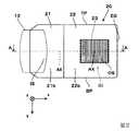
図1に示すように、表示装置100は、画像形成装置10と、導光装置20と、を備える。図1は、図2に示す導光装置20のA−A断面と対応する。
表示装置100は、観察者に虚像としての画像を視認させるとともに、観察者に外界像をシースルーで観察させる。表示装置100において、画像形成装置10と導光装置20とは、観察者の右眼と左眼とに対応して一組ずつ設けられるが、右眼用と左眼用とは左右対称であるため、ここでは左眼用のみを示し、右眼用については図示を省略する。なお、表示装置100は、全体としては、例えば一般の眼鏡のような外観(不図示)を有する。(Overall structure of light guide device and display device)
As shown in FIG. 1, the
The
画像形成装置10は、液晶パネル11と、投射レンズ12と、を備える。液晶パネル11は、光源14からの照明光を空間的に変調し、動画像その他の表示対象となるべき画像光GLを形成する。投射レンズ12は、液晶パネル11上の各点から射出された画像光GLを略平行光線にするコリメートレンズである。投射レンズ12は、ガラスまたはプラスチックで形成され、1枚に限らず、複数枚で構成されていてもよい。投射レンズ12としては、球面レンズに限らず、非球面レンズ、自由曲面レンズ等が用いられてもよい。 The
導光装置20は、平板状の光透過部材を有する。導光装置20は、画像形成装置10で形成された画像光GLを虚像光として観察者の眼EYに向けて射出する一方、外界像を構成する外界光ELを透過させる。導光装置20は、画像光を取り込む入射部21と、主に画像光を導光させる平行導光体22と、画像光GLおよび外界光ELを取り出すための射出部23と、を備える。平行導光体22と入射部21とは、高い光透過性を有する樹脂材料により一体成形されている。第1実施形態の場合、導光装置20を伝播させる画像光GLの光路は、同一回数反射される1種類の光路からなり、複数種類の光路が合成されるものではない。 The
平行導光体22は、観察者の眼EYを基準とする光軸AXに対して傾いて配置されている。平行導光体22の平面22aの法線方向Zは、光軸AXに対して角度κだけ傾いている。これにより、平行導光体22を顔の前面に沿って配置でき、平行導光体22の平面22aの法線は、光軸AXに対して傾きを有する。このように、平行導光体22の平面22aの法線を光軸AXに平行なx方向に対して角度κだけ傾ける場合、光学素子30から射出させる光軸AX上およびその近傍の画像光GL0は、光射出面OSの法線に対して角度κをなす。 The parallel
入射部21は、画像形成装置10からの画像光GLを入射部21内に取り込む光入射面ISと、取り込んだ画像光GLを反射して平行導光体22内に導く反射面RSと、を有する。光入射面ISは、投射レンズ12側に凹の曲面21bから形成されている。曲面21bは、反射面RSで反射された画像光GLを内面側で全反射する機能も有する。 The
反射面RSは、投射レンズ12側に凹の曲面21aから形成されている。反射面RSは、曲面21a上に蒸着法等により成膜されたアルミニウム膜等の金属膜から構成されている。反射面RSは、光入射面ISから入射した画像光GLを反射して光路を折り曲げる。曲面21bは、反射面RSで反射された画像光GLを内側で全反射して光路を折り曲げる。このように、入射部21は、光入射面ISから入射した画像光GLを2回反射させ、光路を折り曲げることにより、画像光GLを平行導光体22の内部に確実に導く。 The reflecting surface RS is formed of a concave
平行導光体22は、y軸に対して平行、かつz軸に対して傾斜した平板状の導光部材であり、導光体とも称される。平行導光体(導光体)22は、光透過性の樹脂材料等により形成され、互いに略平行な一対の平面22a,22bを有する。平面22a,22bは、平行平面であるため、外界像の拡大やフォーカスズレを生じさせることがない。平面22aは、入射部21からの画像光を全反射させる全反射面として機能し、画像光GLを少ない損失で射出部23に導く役割を有する。平面22aは、平行導光体22の外界側に配置されて第1の全反射面として機能し、本明細書中では外界側面とも称する。 The parallel
平面22bは、本明細書中では観察者側面とも称する。平面(観察者側面)22bは、射出部23の一端まで延びている。ここで、平面22bは、平行導光体22と射出部23との境界面IFである(図3参照)。
平行導光体22において、入射部21の反射面RSもしくは光入射面ISで反射された画像光GLは、全反射面である平面22aに入射し、平面22aで全反射され、導光装置20の奥側、すなわち射出部23が設けられた+x側もしくはX側に導かれる。図2に示すように、平行導光体22は、導光装置20の外形のうち、+x側の端面として終端面ESを有する。また、平行導光体22は、±y側の端面として上端面TPおよび下端面BPを有する。 In the parallel
図3に示すように、射出部23は、平行導光体22の奥側(+x側)において、平面22bもしくは境界面IFに沿って板状に構成されている。射出部23は、平行導光体22の外界側の平面(全反射面)22aの領域FRで全反射された画像光GLを通過させる際に、入射した画像光GLを所定の角度で反射して光射出面OS側へ折り曲げる。ここでは、射出部23にこれを透過することなく最初に入射する画像光GLが虚像光としての取出し対象である。つまり、射出部23において光射出面OSの内面で反射される光があっても、これは画像光として利用されない。 As shown in FIG. 3, the
射出部23は、透過性を有する複数のハーフミラーを配列してなる光学素子30を有する。光学素子30の構造については、図4等を参照して後に詳述する。光学素子30は、平行導光体22の観察者側の平面22bに沿って形成されている。 The
導光装置20が以上のような構造を有することから、画像形成装置10から射出され、光入射面ISから導光装置20に入射した画像光GLは、入射部21で複数回の反射によって折り曲げられ、平行導光体22の平面22aの領域FRにおいて全反射されて光軸AXに略沿って進む。+z側の平面22aの領域FRで反射された画像光GLは、射出部23に入射する。 Since the
この際、xy面内において、領域FRの長手方向の幅は、射出部23の長手方向の幅よりも狭い。つまり、画像光GLの光線束が射出部23(または光学素子30)に入射する入射幅は、画像光GLの光線束が領域FRに入射する入射幅よりも広い。このように、画像光GLの光線束が領域FRに入射する入射幅を相対的に狭くすることにより、光路の干渉が生じにくくなり、境界面IFを導光に利用することなく、すなわち、境界面IFで画像光GLを反射させず、領域FRからの画像光GLを射出部23(もしくは光学素子30)に直接入射させることが容易になる。 At this time, in the xy plane, the width in the longitudinal direction of the region FR is smaller than the width in the longitudinal direction of the emitting
射出部23に入射した画像光GLは、射出部23において適度な角度で折り曲げられることで取出し可能な状態となり、最終的に光射出面OSから射出される。光射出面OSから射出された画像光GLは、虚像光として観察者の眼EYに入射する。当該虚像光が観察者の網膜において結像することで、観察者は虚像による画像光GLを認識することができる。 The image light GL that has entered the
ここで、像形成に用いられる画像光GLが射出部23に入射する角度は、光源側の入射部21から離れるに従って大きくなっている。すなわち、射出部23の奥側には、外界側の平面22aに平行なZ方向、または光軸AXに対して傾きの大きな画像光GLが入射して比較的大きな角度で折り曲げられ、射出部23の前側には、Z方向、または光軸AXに対して傾きの小さな画像光GLが入射して比較的小さな角度で折り曲げられる。 Here, the angle at which the image light GL used for image formation is incident on the
(画像光の光路)
以下、画像光の光路について詳しく説明する。
図3に示すように、液晶パネル11の射出面11a上からそれぞれ射出される画像光のうち、破線で示す射出面11aの中央部分から射出される成分を画像光GL0とし、1点鎖線で示す射出面11aの周辺のうち、紙面左側(−xおよび+z側)から射出される成分を画像光GL1とし、2点鎖線で示す射出面11aの周辺のうち、紙面右側(+xおよび−z側)から射出される成分を画像光GL2とする。これらのうち、画像光GL0の光路は光軸AXに沿って延びるものとする。(Optical path of image light)
Hereinafter, the optical path of the image light will be described in detail.
As shown in FIG. 3, among the image lights emitted from the
投射レンズ12を経た画像光GL0,GL1,GL2の主要成分は、導光装置20の光入射面ISからそれぞれ入射した後、入射部21を経て平行導光体22内を通過して射出部23に至る。
具体的には、画像光GL0,GL1,GL2のうち、射出面11aの中央部分から射出された画像光GL0は、入射部21で折り曲げられて平行導光体22内に結合された後、標準反射角θ0で一方の平面22aの領域FRに入射して全反射され、平行導光体22と射出部23(もしくは光学素子30)との境界面IFで反射されずに境界面IFを通過し、射出部23の中央の部分23kに直接的に入射する。画像光GL0は、部分23kにおいて所定の角度で反射され、光射出面OSから光射出面OSを含むXY面に対して傾いた光軸AX方向(Z方向に対して角度κの方向)に平行光束として射出される。The main components of the image lights GL0, GL1, and GL2 that have passed through the
Specifically, of the image lights GL0, GL1, and GL2, the image light GL0 emitted from the central portion of the
射出面11aの一端側(−x側)から射出された画像光GL1は、入射部21で折り曲げられて平行導光体22内に結合された後、最大反射角θ1で平面22aの領域FRに入射して全反射され、平行導光体22と射出部23(もしくは光学素子30)との境界面IFで反射されずに境界面IFを通過し、射出部23のうち、奥側(+x側)の部分23hにおいて所定の角度で反射され、光射出面OSから所定の角度方向に向けて平行光束として射出される。この際の射出角γ1は、入射部21側に戻される角度が相対的に大きくなっている。 The image light GL1 emitted from one end side (−x side) of the
一方、射出面11aの他端側(+x側)から射出された画像光GL2は、入射部21で折り曲げられて平行導光体22内に結合された後、最小反射角θ2で平面22aの領域FRに入射して全反射され、平行導光体22と射出部23(もしくは光学素子30)との境界面IFで反射されずに境界面IFを通過し、射出部23のうち、入口側(−x側)の部分23mにおいて所定の角度で反射され、光射出面OSから所定の角度方向に向けて平行光束として射出される。この際の射出角γ2は、入射部21側に戻される角度が相対的に小さくなっている。 On the other hand, the image light GL2 emitted from the other end side (+x side) of the
なお、画像光GL0,GL1,GL2は、画像光GLの光線全体の一部を代表して説明したものであるが、他の画像光GLを構成する光線成分についても画像光GL0等と同様に導かれ、光射出面OSから射出される。そのため、これらについては図示および説明を省略する。 Note that the image lights GL0, GL1, and GL2 have been described as representatives of a part of the entire light rays of the image light GL, but the light ray components that make up the other image light GL are similar to the image light GL0 and the like. The light is guided and emitted from the light emission surface OS. Therefore, illustration and description of these are omitted.
ここで、入射部21および平行導光体22に用いられる透明樹脂材料の屈折率nの値の一例として、n=1.4とすると、臨界角θcの値はθc≒45.6°となる。画像光GL0,GL1,GL2の反射角θ0,θ1,θ2のうち、最小である反射角θ2を臨界角θcよりも大きな値とすることにより、必要な画像光について全反射条件を満たすものにできる。 Here, assuming that n=1.4 as an example of the value of the refractive index n of the transparent resin material used for the
中央向けの画像光GL0は、仰角φ0(=90°−θ0)で射出部23の部分23kに入射する。周辺向けの画像光GL1は、仰角φ1(=90°−θ1)で射出部23の部分23hに入射する。周辺向けの画像光GL2は、仰角φ2(=90°−θ2)で射出部23の部分23mに入射する。ここで、仰角φ0,φ1,φ2間には、反射角θ0,θ1,θ2の大小関係を反映して、φ2>φ0>φ1の関係が成り立っている。すなわち、光学素子30のハーフミラー31への入射角ι(図4参照)は、仰角φ2に対応する部分23m、仰角φ0に対応する部分23k、仰角φ1に対応する部分23hの順で徐々に小さくなる。換言すれば、ハーフミラー31への入射角ιもしくはハーフミラー31での反射角は、入射部21から離れるに従って小さくなる。 The image light GL0 directed to the center is incident on the
平行導光体22の外界側の平面22aで反射されて射出部23に向かう画像光GLの光線束の全体的な挙動について説明する。
図3に示すように、画像光GLの光線束は、光軸AXを含む断面において、平行導光体22の外界側の領域FRで反射される前後の直進光路P1,P2のいずれかで幅が絞られる。具体的には、画像光GLの光線束は、光軸AXを含む断面において、領域FR近辺、つまり直進光路P1,P2の境界付近で直進光路P1,P2に跨るような位置で全体として幅が絞られてビーム幅が細くなっている。これにより、画像光GLの光線束を射出部23の手前で絞ることになり、横方向の視野角を比較的広くすることが容易になる。
なお、図示の例では、画像光GLの光線束が直進光路P1,P2に跨るような位置で幅が絞られてビーム幅が細くなっているが、直進光路P1,P2のいずれか片側のみで幅が絞られてビーム幅が細くなってもよい。The overall behavior of the light beam bundle of the image light GL that is reflected by the
As shown in FIG. 3, in the cross section including the optical axis AX, the ray bundle of the image light GL has a width in any of the straight optical paths P1 and P2 before and after being reflected by the region FR on the external side of the parallel
In the illustrated example, the beam width of the image light GL is narrowed and narrowed at a position where the light flux of the image light GL straddles the straight-ahead optical paths P1 and P2, but only on one side of the straight-ahead optical paths P1 and P2. The width may be narrowed to narrow the beam width.
(光学素子の構成)
以下、図3〜図5を参照して、射出部23を構成する光学素子30の構成について説明する。
射出部23は、平行導光体22の視認側の面に設けられた光学素子30で構成されている。したがって、射出部23は、平行導光体22と同様に、光軸AXに対して角度κだけ傾いたXY平面に沿って設けられている。光学素子30は、複数のハーフミラー31と、複数の透光性部材32と、を備える。光学素子30は、複数の透光性部材32が、隣り合う2つの透光性部材32の間にそれぞれハーフミラー31を挟持した構成を有する。換言すると、光学素子30は、ハーフミラー31と透光性部材32とが交互に配置された構成を有する。(Structure of optical element)
Hereinafter, the configuration of the
The emitting
図5は、光学素子30を、一対の透光性部材32とハーフミラー31の組毎に分解した状態で示す斜視図である。
図5に示すように、透光性部材32は、長手方向に垂直な断面形状が平行四辺形の柱状の部材である。したがって、透光性部材32は、長手方向に平行に延び、互いに平行な一対の平面を2組有している。これら2組の一対の平面のうち、一方の組の一方の平面が画像光GLおよび外界光ELを入射させる入射面32aであり、一方の組の他方の平面が画像光GLおよび外界光ELを射出させる射出面32bである。また、他方の組の一方の平面に、膜厚が異なる領域31A,31B,31Cを有するハーフミラー31が設けられている。透光性部材32は、例えばガラス、透明樹脂等により構成されている。FIG. 5 is a perspective view showing the
As shown in FIG. 5, the
複数の透光性部材32は、全て同じ形状、同じ寸法に構成されている。そのため、一対の透光性部材32とハーフミラー31からなる組を複数貼り合わせると、複数のハーフミラー31は、互いに平行に配置された形態となる。図4および図5では図示を省略するが、ハーフミラー31の一方の面と隣り合う透光性部材32との間には、接着材層が設けられている。これにより、光学素子30は、全体として矩形板状の部材となる。透光性部材32の入射面32aもしくは射出面32bの法線方向から光学素子30を見ると、細い帯状の複数のハーフミラー31がストライプ状に並べられた構造となる。すなわち、光学素子30は、矩形状のハーフミラー31が平行導光体22の延びる方向、すなわちX方向に所定の間隔(ピッチPT)をおいて複数配列された構成を有する。 The plurality of
なお、図4に示すように、ハーフミラー31の一方の面は平坦な面であり、他方の面は膜厚差分の段差を有する面であるから、厳密に言えば、隣り合うハーフミラー31同士は互いに平行であるとは言いにくい。しかしながら、本発明では、ハーフミラーの少なくとも一方の面が平行であるとき、複数のハーフミラーが互いに平行であるとみなす。ハーフミラーは薄膜で構成され、膜厚差分も僅かであるため、膜厚差分を無視すれば、複数のハーフミラーが互いに平行であると言って差し支えない。 Note that, as shown in FIG. 4, one surface of the
ハーフミラー31は、透光性部材32間に挟まれた反射膜で構成されている。反射膜として、例えばアルミニウム等の反射率が高い金属膜が用いられる。反射膜の厚さは十分に薄いため、ハーフミラー31は、光学素子30に入射した画像光GLおよび外界光ELの一部を反射させ、画像光GLおよび外界光ELの他の一部を透過させる。なお、反射膜として、屈折率が異なる誘電体薄膜が交互に複数層積層された誘電体多層膜が用いられてもよい。 The
ハーフミラー31は、ハーフミラー31の短辺が透光性部材の入射面32aおよび射出面32bに対して傾斜して設けられている。より具体的には、ハーフミラー31は、平行導光体22の外界側に向かって反射面31rが入射部21側を向くように傾斜している。換言すると、ハーフミラー31は、ハーフミラー31の長辺(Y方向)を軸として、平面22a,22bに直交するYZ面を基準として上端(+Z側)が反時計周りに回転する方向に傾斜している。 The
以下、ハーフミラー31の反射面31rと透光性部材32の射出面32bとのなす角度をハーフミラー31の傾斜角度δと定義する。本実施形態において、ハーフミラー31の傾斜角度δは、45°以上、90°未満である。本実施形態では、透光性部材32の屈折率と平行導光体22の屈折率とは等しいが、これらの屈折率は異なっていてもよい。屈折率が異なる場合、屈折率が等しい場合に対してハーフミラー31の傾斜角度δを変更する必要がある。 Hereinafter, the angle formed by the reflecting
ハーフミラー31は、傾斜方向に沿って反射率が異なる複数の領域31A,31B,31Cを有する。図4の例では、反射膜として金属膜を用いており、ハーフミラー31は、傾斜方向に沿って膜厚が異なる複数の領域を有する金属膜で構成される。各領域31A,31B,31Cにおける金属膜の膜厚は、例えば10nm、20nm、30nmである。この例では、ハーフミラー31は、反射率が異なる3つの領域31A,31B,31Cを有するが、領域の数は3に限ることなく、領域の数は2以上であればよい。また、ハーフミラーは、反射率が段階的に異なる領域を有するのではなく、反射率が連続的に異なっていてもよい。反射率が連続的に異なる場合も、ハーフミラーは膜厚が異なる複数の領域を有する、という概念に含まれる。 The
上述したように、反射膜として金属膜を用いた場合、領域によって膜厚を異ならせることにより、反射率を異ならせることが可能である。また、反射膜として誘電体多層膜を用いた場合には、領域によって誘電体多層膜の1層分の膜厚、積層数、誘電体材料のいずれかを異ならせることにより、反射率を異ならせることが可能である。 As described above, when a metal film is used as the reflective film, it is possible to make the reflectance different by making the film thickness different depending on the region. When a dielectric multilayer film is used as the reflective film, the reflectance is changed by changing the thickness of one dielectric multilayer film, the number of layers, or the dielectric material depending on the region. It is possible.
本実施形態のように、ハーフミラー31の傾斜角度δが45°以上で90°未満である場合、傾斜方向において射出面32bに近い側に、反射率が相対的に高い高反射率領域31Aが設けられている。また、傾斜方向において高反射率領域31Aよりも射出面32bから遠い側に、高反射率領域31Aの反射率よりも低い反射率を有する低反射率領域31Cが設けられている。また、高反射率領域31Aと低反射率領域31Cとの間に、高反射率領域31Aの屈折率と低反射率領域31Cの屈折率との間の屈折率を有する中間反射率領域31Bが設けられている。すなわち、入射面32aから射出面32bに向けて、低反射率領域31C、中間反射率領域31B、高反射率領域31Cがこの順に設けられている。 When the inclination angle δ of the
なお、光学素子30におけるハーフミラー31のピッチPTは、0.5mm〜2.0mm程度に設定される。また、図4に示すように、光学素子30においては、ハーフミラー31のピッチが若干広めに設定され、外界光ELの一部がハーフミラー31に入射することなく、光学素子30を透過する。この場合、ハーフミラー31のピッチを適宜調整することにより、外界光ELが光学素子30を直接的に透過することを回避できる。 The pitch PT of the
ハーフミラー31のピッチPTは、厳密には等間隔でなく、可変ピッチで配置されている。より具体的には、光学素子30におけるハーフミラー31のピッチPTは、基準間隔を中心としてランダムに増減するランダムピッチとなっている。このように、光学素子30におけるハーフミラー31をランダムピッチで配置することにより、回折ムラやモアレの発生を抑制することができる。なお、ランダムピッチに限らず、例えば複数段階で増減するピッチを含む所定のピッチパターンを繰り返すものであってもよい。 Strictly speaking, the pitch PT of the
ここで、光学素子30の厚み、即ちハーフミラー31のZ軸方向の厚みTIは、0.7mm〜3.0mm程度に設定される。なお、光学素子30を支持する平行導光体22の厚みは、例えば数mm〜10mm程度、好ましくは4mm〜6mm程度となっている。平行導光体22の厚みが光学素子30の厚みに比較して十分大きいと、光学素子30または境界面IFへの画像光GLの入射角を小さくしやすく、画像光GLが眼EYに取り込まれない位置にあるハーフミラー31での反射を抑えやすい。一方、平行導光体22の厚みを比較的薄くすると、平行導光体22や導光装置20の軽量化を図りやすくなる。 Here, the thickness of the
(光学素子の製造方法)
以下、図6A〜図6C、図7A〜図7B、図8を参照して、光学素子30の製造方法の一例について説明する。
光学素子30の製造方法は、要素板作製工程と、積層体作製工程と、個片化(光学素子作製)工程と、を有する。要素板作製工程は、透光性基板の一面に、マスクを用いて反射率が異なる複数の領域を有するハーフミラーを形成し、ハーフミラーが形成された透光性基板からなる要素板を作製する工程である。積層体作製工程は、複数の要素板を、ハーフミラーを同じ方向に向けて積層し、複数の要素板が積層された積層体を作製する工程である。個片化(光学素子作製)工程は、積層体を、ハーフミラーの各々が切断面に対して傾斜し、ハーフミラーの反射率が異なる複数の領域が傾斜方向に沿って配置されるように切断し、個片化した光学素子を作製する工程である。(Method of manufacturing optical element)
Hereinafter, an example of a method for manufacturing the
The manufacturing method of the
最初に、第1成膜工程として、図6Aに示すように、ガラス板等の透光性基板51を準備し、マスク52を用いた蒸着法、スパッタ法等により、透光性基板51の一面に例えばアルミニウム等の金属膜53aを例えば10nmの膜厚で成膜する。 First, as a first film forming step, as shown in FIG. 6A, a
次に、第2成膜工程として、図6Bに示すように、第1成膜工程で金属膜53aを成膜した領域からマスク52を遠ざける方向(図における左方向)に移動させ、透光性基板51の一面に同一材料の金属膜53bを成膜する。このとき、この工程で新たに露出した透光性基板51の一面に金属膜53bが成膜されるとともに、第1成膜工程で既に成膜された金属膜53aの上にはさらに金属膜53bが積層される。そのため、2段階の膜厚を有する金属膜が形成される。膜厚の差は例えば10nm程度とする。 Next, as a second film forming step, as shown in FIG. 6B, the
次に、第3成膜工程として、図6Cに示すように、第2成膜工程で金属膜53bを成膜した領域からマスク52を遠ざける方向(図における左方向)に移動させ、透光性基板51の一面に同一材料の金属膜53cを成膜する。このとき、この工程で新たに露出した透光性基板51の一面に金属膜53cが成膜され、第2成膜工程で成膜された金属膜53bの上にさらに金属膜53cが積層され、第1成膜工程および第2成膜工程で既に成膜された金属膜53a,53bの上にはさらに金属膜53cが積層される。これにより、3段階の膜厚、すなわち3種類の反射率を有する金属膜53が透光性基板51上に形成された要素板90が作製される。膜厚の差は例えば10nm程度とする。 Next, as a third film forming step, as shown in FIG. 6C, the
また、反射膜として誘電体多層膜を用いる場合には、以下の方法を採用してもよい。
最初に、第1成膜工程として、図7Aに示すように、ガラス板等の透光性基板51を準備し、マスク52を用いた蒸着法、スパッタ法等により、透光性基板51の一面に誘電体多層膜54aを成膜する。When a dielectric multilayer film is used as the reflective film, the following method may be adopted.
First, as a first film forming step, as shown in FIG. 7A, a
次に、第2成膜工程として、図7Bに示すように、第1成膜工程で誘電体多層膜54aを成膜した領域にマスク52を移動させ、第1成膜工程で誘電体多層膜54aを成膜しなかった領域に、第1成膜工程とは異なる誘電体多層膜54bを成膜する。このとき、誘電体多層膜54a,54bの1層分の膜厚、積層数、誘電体材料のいずれかを異ならせればよい。これにより、反射率が異なる領域を有する誘電体多層膜54が透光性基板51上に形成された要素板90Aが作製される。 Next, as a second film forming step, as shown in FIG. 7B, the
次に、図8に示すように、複数の要素板90を接着剤で貼り合わせ、積層体92を作製する。その後、要素板90の一面に対して傾斜した切断線C1、C2に沿って、積層体92を斜めに切断する。これにより、積層体92が個片化され、細長いプリズム状の透光性部材32の間にハーフミラー31が挟持された構造の光学素子30が完成する。 Next, as shown in FIG. 8, a plurality of
さらに光学素子30を平行導光体22に取り付ける際には、図3に示すように、光学素子30を、平行導光体22の視認側の平面22bの所定の位置に接着剤を介して貼り付けた後、接着剤を硬化させて固定する。 Further, when attaching the
(光学素子の作用)
図3、図4等に示すように、複数のハーフミラー31は、例えば48°〜70°程度の傾斜角度δを有し、具体的には、例えば60°の傾斜角度δを有している。ここで、画像光GL0の仰角φ0が例えば30°に設定され、画像光GL1の仰角φ1が例えば22°に設定され、画像光GL2の仰角φ2が例えば38°に設定されているものとする。この場合、画像光GL1と画像光GL2とは、光軸AXを基準として角度γ1=γ2≒12.5°をもって観察者の眼EYに入射する。(Function of optical element)
As shown in FIGS. 3 and 4, the plurality of half mirrors 31 have an inclination angle δ of, for example, about 48° to 70°, and specifically have an inclination angle δ of, for example, 60°. .. Here, it is assumed that the elevation angle φ0 of the image light GL0 is set to, for example, 30°, the elevation angle φ1 of the image light GL1 is set to, for example, 22°, and the elevation angle φ2 of the image light GL2 is set to, for example, 38°. In this case, the image light GL1 and the image light GL2 enter the observer's eye EY at an angle γ1=γ2≈12.5° with respect to the optical axis AX.
これにより、上記画像光GLのうち全反射角度の比較的大きい成分(画像光GL1)を光学素子30のうち−x側の部分23h側に主に入射させ、全反射角度の比較的小さい成分(画像光GL2)を射出部23のうち+x側の部分23m側に主に入射させた場合において、画像光GLを全体として観察者の眼EYに集めるような角度で効率的に取り出すことができる。光学素子30はこのような角度の関係で画像光GLを取り出す構成であるため、導光装置20は、画像光GLを光学素子30において原則として複数回経由させず、1回だけ経由させることができる。そのため、光学素子30は、画像光GLを少ない損失で虚像光として取り出すことができる。 As a result, a component of the image light GL having a relatively large total reflection angle (image light GL1) is mainly incident on the −x
なお、光学素子30の中央側や奥側の部分23k,23h等において、画像光GLのごく一部は、ハーフミラー31を複数回経由(具体的には、1回の反射と1回以上の透過を含む通過)している。この場合、ハーフミラー31の経由回数が複数になるが、複数のハーフミラー31からの反射光が、画像光GLとして観察者の眼EYにそれぞれ入射するため、光量の損失はあまり大きくはならない。 It should be noted that in the
また、光学素子30の中央側や奥側の部分23k,23h等において、画像光GLのうち、平行導光体22の裏側または観察者側(つまり、光射出面OS、境界面IF等)で反射される成分も発生する可能性がある。しかしながら、このような画像光GLは、ハーフミラー31で反射される非利用光GX(図4参照)として光路外に導かれるようになっており、観察者の眼EYに入射することが回避される。なお、ハーフミラー31を通過する非利用光は、外界側の平面22aに再度入射するおそれがある。ところが、ここで全反射された場合、多くは光学素子30の奥側の部分23h、またはさらに奧側の有効領域外に入射させることができ、眼EYに入射するおそれが低減される。 Further, in the
(本実施形態の効果:画像光に対する効果)
以下、本実施形態の光学素子の特有の効果について説明する。
図9は、画像光GLに対する光学素子30の作用を説明するためのモデルを示す図である。ここでは、説明をわかりやすくするため、反射率が異なる2つの領域を有するハーフミラー311〜314を想定する。ハーフミラー311〜314の傾斜角度δは45°以上、90°未満である。
ハーフミラー311〜314の反射率が異なる2つの領域のうち、射出面32bから遠い側の第1領域(低反射率領域)の反射率をpとする。射出面32bに近い側の第2領域(高反射率領域)の反射率をqとする。(Effect of this embodiment: Effect on image light)
The effects peculiar to the optical element of this embodiment will be described below.
FIG. 9 is a diagram showing a model for explaining the action of the
Of the two regions having different reflectances of the half mirrors 311 to 314, the reflectance of the first region (low reflectance region) farther from the
光学素子30の入射面32aに対して仰角φ0で入射する画像光GLを考える。
画像光GLは、入射面32aから入射した後、光学素子30の内部を伝播し、第1のハーフミラー311、第2のハーフミラー312、第3のハーフミラー313、第4のハーフミラー314の順に到達する。第1のハーフミラー311に入射した光のうち、一部の光は、第1のハーフミラー311の第1領域311Aで反射して光路を曲げた後、射出面32bから射出されるとともに、残りの光は、第2のハーフミラー312に向けて進む。Consider the image light GL incident on the
The image light GL, after being incident from the
また、第1のハーフミラー311を透過した光のうち、一部の光は、第2のハーフミラー312の第1領域312Aで反射して光路を曲げた後、射出面32bから射出されるとともに、残りの光は、第3のハーフミラー313に向けて進む。また、第2のハーフミラー312を透過した光のうち、一部の光は、第3のハーフミラー313の第2領域313Bで反射して光路を曲げた後、射出面32bから射出されるとともに、残りの光は、第4のハーフミラー314に向けて進む。また、第3のハーフミラー313を透過した光のうち、一部の光は、第4のハーフミラー314の第2領域314Bで反射して光路を曲げた後、射出面32bから射出される。 In addition, a part of the light transmitted through the
ここで、第1のハーフミラー311から射出される光GLAの相対強度をIAとし、第2のハーフミラー312から射出される光GLBの相対強度をIBとし、第3のハーフミラー313から射出される光GLCの相対強度をICとし、第4のハーフミラー314から射出される光GLDの相対強度をIDとする。なお、光学素子30に入射する画像光GLの強度を1としたときの各射出光GLA、GLB、GLC、GLDの強度を相対強度と定義する。Here, the relative intensity of the light GLA emitted from the
相対強度IA〜IDは、それぞれ以下の(1)〜(4)式で表される。
相対強度IA:IA=p …(1)
相対強度IB:IB=(1−p)×p …(2)
相対強度IC:IC=(1−p)×(1−p)×q …(3)
相対強度ID:ID=(1−p)×(1−p)×(1−q)×q …(4)The relative intensities IA to ID are represented by the following equations (1) to (4), respectively.
Relative intensity IA : IA =p (1)
Relative intensity IB : IB =(1−p)×p (2)
Relative intensity IC : IC =(1−p)×(1−p)×q (3)
Relative intensity ID : ID =(1-p)×(1-p)×(1-q)×q (4)
実施例の一例として、反射率p、反射率qがそれぞれ、p=0.22、q=0.28のハーフミラーを想定する。また、比較例として、p=q=0.25のハーフミラーを想定する。すなわち、比較例は、反射率が一様なハーフミラーである。これらの反射率の値を(1)〜(4)式に代入して、各射出光の相対強度IA〜IDを算出した。その結果を図10に示す。As an example of the embodiment, a half mirror whose reflectance p and reflectance q are p=0.22 and q=0.28 is assumed. As a comparative example, a half mirror with p=q=0.25 is assumed. That is, the comparative example is a half mirror having a uniform reflectance. Substituting these reflectance values into the equations (1) to (4), the relative intensities IA to ID of the respective emitted lights were calculated. The result is shown in FIG.
図10において、符号○で示す点は、実施例における各射出光の相対強度IA〜IDである。符号×で示す点は、比較例における各射出光の相対強度IA〜IDである。図10に示すように、比較例の場合、相対強度IA〜IDの最大値と最小値との差が約0.14であるのに対し、実施例の場合、相対強度IA〜IDの最大値と最小値との差が約0.10であった。このように、射出面(観察者)から遠い側の領域の反射率を相対的に小さく、射出面に近い側の領域の反射率を相対的に大きくすると、反射率が一様な場合に比べて、相対強度IA〜IDの差を低減できることがわかった。In FIG. 10, the points indicated by the symbol ◯ are the relative intensities IA to ID of the respective emitted lights in the example. The points indicated by the symbol x are the relative intensities IA to ID of the respective emitted lights in the comparative example. As shown in FIG. 10, in the case of the comparative example, whereas the difference between the maximum and minimum values of the relative intensitiesI A ~ID is about 0.14, in the embodiment, the relative intensityI A ~I The difference between the maximum value and the minimum value ofD was about 0.10. In this way, when the reflectance of the area far from the exit surface (observer) is relatively small and the reflectance of the area near the exit surface is relatively large, it is compared to the case where the reflectance is uniform. It was found that the difference between the relative intensities IA to ID can be reduced.
ここでは説明を簡単にするため、反射率が異なる2つの領域を有するハーフミラー311〜314の例を挙げたが、反射率が異なる領域の数が3つ以上であった場合であっても同様の結果が得られる。本実施形態のように、反射率が異なる2つ以上の領域を有するハーフミラー31を備えた光学素子30を用いることにより、眼の位置が移動しても、縞状の模様が視認されにくい表示装置100を実現することができる。 Here, for simplification of description, an example of the half mirrors 311 to 314 having two regions having different reflectances has been described, but the same applies even when the number of regions having different reflectances is three or more. The result of is obtained. By using the
なお、反射率が一様であっても、反射率の値を全体的に小さくすれば、相対強度の差は小さくなる。しかしながら、その場合には相対強度の総和が小さくなるため、画像光GLの利用効率が低下し、画像が暗くなるという欠点がある。例えば上記の例でp=q=0.20とした場合、相対強度IA〜IDの最大値と最小値との差は実施例とほぼ同等となるが、相対強度IA〜IDの総和は約0.59となる。一方、実施例の場合、相対強度IA〜IDの総和は約0.68である。したがって、明るい画像を得るためには実施例のハーフミラーを用いることが好ましい。Even if the reflectance is uniform, if the value of the reflectance is made small as a whole, the difference in relative intensity becomes small. However, in that case, the sum of the relative intensities becomes small, so that there is a drawback that the utilization efficiency of the image light GL decreases and the image becomes dark. For example, if the p = q = 0.20 in the above example, the difference between the maximum and minimum values of the relative intensitiesI A ~ID is approximately equal to Example, the relative intensityI A ~ID The total sum is about 0.59. On the other hand, in the case of the example, the total sum of the relative intensities IA to ID is about 0.68. Therefore, it is preferable to use the half mirror of the embodiment in order to obtain a bright image.
さらに、光学素子30の全体に対して詳細なシミュレーションを行った結果を図11に示す。図11の横軸は光学素子の位置(mm)を示し、図11の縦軸は相対強度(a.u.)を示す。光学素子30の位置は、長手方向の中心を0(mm)とし、入射部に近い側の端部の位置を−9(mm)とし、入射部とは反対側の端部の位置を+9(mm)とする。 Further, FIG. 11 shows the result of detailed simulation performed on the entire
図11において、符号Aで示す実線のグラフは実施例における相対強度の分布を示し、符号Bで示す破線のグラフは比較例における相対強度の分布を示す。
図11に示すように、反射率が異なる領域を設けた実施例の場合、反射率が一様な比較例に比べて、相対強度の高低の差が小さくなっていることがわかった。光学素子30のうち、特に入射部21に近い側における効果が顕著であった。In FIG. 11, the solid line graph indicated by reference symbol A shows the relative intensity distribution in the example, and the broken line graph indicated by reference symbol B shows the relative intensity distribution in the comparative example.
As shown in FIG. 11, in the case of the example in which the regions having different reflectances were provided, it was found that the difference in relative intensity was smaller than that in the comparative example having uniform reflectance. The effect of the
(本実施形態の効果:外界光に対する効果)
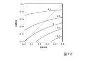
図12は、外界光ELに対する光学素子30の作用を説明するためのモデルを示す図である。ここでは、説明をわかりやすくするため、反射率が異なる2つの領域を有するハーフミラー311,312を想定する。ハーフミラー311,312の傾斜角度δは45°以上、90°未満である。
ハーフミラー311,312の反射率が異なる2つの領域のうち、射出面から遠い側の第1領域の反射率をpとし、射出面に近い側の第2領域の反射率をqとする。(Effect of this embodiment: Effect on external light)
FIG. 12 is a diagram showing a model for explaining the action of the
Of the two regions having different reflectances of the half mirrors 311 and 312, the reflectance of the first region on the side far from the emission surface is p, and the reflectance of the second region on the side closer to the emission surface is q.
外界光ELは、画像光GLとは異なり、光学素子30の入射面32aに対して垂直に近い角度で入射する。また、観察者の瞳に入射する光として、第1のハーフミラー311を透過する光EL1、第1のハーフミラー311で1回反射した光EL12、の2本の光線を考える。
光EL1のうち、一部の光は、入射面32aから入射した後、第1のハーフミラー311に入射する。第1のハーフミラー311に入射した光のうち、一部の光ELaは、第1のハーフミラー311の第1領域311Aを透過して射出面32bから射出される。他の光は、第1のハーフミラー311の第1領域311Aで反射して第2のハーフミラー312の第2領域312Bに向かって進む。Unlike the image light GL, the external light EL is incident on the
Part of the light EL1 enters the
第1のハーフミラー311の第1領域311Aで反射した光EL12は、第2のハーフミラー312の第2領域312Bで反射する。また、第2のハーフミラー312の反射位置には、第2のハーフミラー312に直接入射した光EL2も到達する。そのため、第2のハーフミラー312の反射位置からは、第1のハーフミラー311の第1領域311Aで反射し、さらに第2のハーフミラー312の第2領域312Bで反射した光EL12、および第2のハーフミラー312の第2領域312Bに直接入射して透過した光EL2の双方が射出される。観察者は、これらの光EL12,EL2が合成された光ELbを見ることになる。 The light EL12 reflected by the
ここで、第1のハーフミラー311から射出された光ELaの相対強度をIaとし、第2のハーフミラー312から射出された光ELbの相対強度をIbとする。
相対強度Ia、Ibは、それぞれ以下の(5)、(6)式で表される。
相対強度Ia:Ia=1−p …(5)
相対強度Ib:Ib=(1−q)+p×q …(6)Here, the relative intensity of light emitted ELa from the
The relative intensities Ia and Ib are represented by the following equations (5) and (6), respectively.
Relative intensity Ia : Ia =1−p (5)
Relative intensity Ib : Ib =(1−q)+p×q (6)
これら2つの光の相対強度Ia、Ibの差が大きい場合、微細な明暗の縞模様が形成され、光の回折が生じる。その結果、外界の像がぼけるという問題が発生する。したがって、観察者が鮮明な外界の像を視認するためには、相対強度Ia、Ibの差を小さくする必要がある。When the difference between the relative intensities Ia and Ib of these two lights is large, a fine light and dark stripe pattern is formed, and light diffraction occurs. As a result, the problem that the image of the outside world is blurred occurs. Therefore, in order for the observer to visually recognize a clear image of the outside world, it is necessary to reduce the difference between the relative intensities Ia and Ib .
図13は、反射率pおよび反射率qを種々の値に変化させたときの相対強度Ia、Ibの差を示す図である。図13の横軸は反射率qの値であり、図13の縦軸は反射率pの値である。図13中には、相対強度差が0、±0.3、±0.7のときの5本の曲線を示す。FIG. 13 is a diagram showing the difference between the relative intensities Ia and Ib when the reflectance p and the reflectance q are changed to various values. The horizontal axis of FIG. 13 is the value of reflectance q, and the vertical axis of FIG. 13 is the value of reflectance p. FIG. 13 shows five curves when the relative intensity difference is 0, ±0.3, and ±0.7.
図13に示すように、反射率pと反射率qとの大小関係がp<qを満たす場合、相対強度差の絶対値が小さくなることがわかった。すなわち、光学素子30の射出面32b(観察者)から遠い側の領域の反射率を相対的に小さく、射出面32bに近い側の領域の反射率を相対的に大きくすることにより相対強度差を小さくすることができる。これにより、外界の像のボケを低減することができる。 As shown in FIG. 13, it was found that the absolute value of the relative intensity difference becomes small when the magnitude relation between the reflectance p and the reflectance q satisfies p<q. That is, by making the reflectance of the area of the
(本実施形態の効果のまとめ)
以上述べたように、本実施形態の光学素子30においては、複数のハーフミラー31の各々が傾斜方向に反射率が異なる複数の領域31A,31B,31Cを有し、光学素子30の射出面(観察者)から遠い側に低反射率領域31Cが設けられ、射出面に近い側に高反射率領域31Aが設けられている。これにより、画像光による縞状の模様を低減できる効果、外界の像のボケを低減できる効果、の2つの効果が得られる。したがって、本実施形態の表示装置100は光学素子30を備えたことにより、表示品質が高く、シースルー性に優れた表示装置100を実現することができる。(Summary of effects of this embodiment)
As described above, in the
なお、第1実施形態では、平行導光体22が眼を通る光軸AXに垂直なxy面に対して傾斜しているが、平行導光体22をxy面に平行に配置してもよい。また、入射部21を曲面21a,21bで構成しているが、その一方または双方を平面で構成することもできる。この場合、曲面21bに対応する部分を平行導光体22の平面22bを延長した平面とすることができる。また、入射部21において、光入射面ISから入射させた画像光GLを内面で反射させずに、そのまま平行導光体22に結合する構成とすることもできる。 In the first embodiment, the parallel
さらに、平行導光体22は、完全な平行平板に限らず、若干の湾曲や楔角を持たせることができる。つまり、平行導光体22の平面22a,22bを非球面その他の湾曲面としたり、相互に傾き角を形成したりすることができる。ただし、平面22a,22bを湾曲させた場合、視度や倍率変化が発生するので、湾曲は少ない方が良い。また、平面22a,22b間に傾きを設けた場合、色分散が生じるので、傾き角は小さい方が望ましい。 Further, the parallel
[第2実施形態]
以下、本発明の第2実施形態について、図14および図15を用いて説明する。
第2実施形態の表示装置の基本構成は第1実施形態と同様であり、光学素子の構成が第1実施形態と異なる。そのため、表示装置全体の説明は省略し、光学素子についてのみ説明する。
図14は、第2実施形態の光学素子の断面図である。図14は、第1実施形態における図4に対応している。
図14において、図4と共通の構成要素には同一の符号を付し、説明を省略する。[Second Embodiment]
The second embodiment of the present invention will be described below with reference to FIGS. 14 and 15.
The basic configuration of the display device of the second embodiment is the same as that of the first embodiment, and the configuration of the optical element is different from that of the first embodiment. Therefore, the description of the entire display device will be omitted, and only the optical element will be described.
FIG. 14 is a sectional view of the optical element of the second embodiment. FIG. 14 corresponds to FIG. 4 in the first embodiment.
14, the same components as those of FIG. 4 are designated by the same reference numerals, and the description thereof will be omitted.
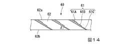
(光学素子の構成)
図14に示すように、第2実施形態の光学素子60は、複数のハーフミラー61と、複数の透光性部材62と、を備える。第2実施形態の光学素子60において、ハーフミラー61の傾斜角度δは、45°未満である。本実施形態のように、ハーフミラー61の傾斜角度δが45°未満である場合、第1実施形態とは逆に、ハーフミラー61の傾斜方向において射出面62bに近い側に、反射率が相対的に低い低反射率領域61Cが設けられている。また、傾斜方向において低反射率領域61Cよりも射出面62bから遠い側に反射率が低反射率領域61Cよりも高い高反射率領域61Aが設けられている。また、低反射率領域61Cと高反射率領域61Aとの間に、低反射率領域61Cの屈折率と高反射率領域61Aの屈折率との間の屈折率を有する中間反射率領域61Bが設けられている。すなわち、光学素子60の入射面62aから射出面62bに向けて、高反射率領域61A、中間反射率領域61B、低反射率領域61Cがこの順に設けられている。
その他の構成は、第1実施形態と同様である。(Structure of optical element)
As shown in FIG. 14, the
Other configurations are similar to those of the first embodiment.
(本実施形態の効果:外界光に対する効果)
以下、本実施形態の光学素子60の特有の効果について説明する。
図15は、外界光ELに対する光学素子60の作用を説明するためのモデルを示す図である。ここでは、説明をわかりやすくするため、反射率が異なる2つの領域を有するハーフミラー611,612を想定する。ハーフミラー611,612の傾斜角度δは、45°未満である。
ハーフミラー611,612の2つの領域のうち、射出面62bから遠い側の第1領域の反射率をpとし、射出面62bに近い側の第2領域の反射率をqとする。(Effect of this embodiment: Effect on external light)
Hereinafter, effects peculiar to the
FIG. 15 is a diagram showing a model for explaining the action of the
Of the two areas of the half mirrors 611 and 612, the reflectance of the first area far from the
観察者の瞳に入射する光として、第1のハーフミラー611を透過した光ELa、第1のハーフミラー611で1回反射した光EL12、の2本の光線を考える。
光EL1のうち、一部の光は、入射面62aから入射した後、第1のハーフミラー611に入射する。第1のハーフミラー611に入射した光のうち、一部の光は、第1のハーフミラー611の第2領域611Bを透過して射出面62bから射出される。他の光は、第1のハーフミラー611の第2領域611Bで反射して第2のハーフミラー612の第1領域612Aに向かって進む。As light entering the observer's pupil, two light rays, a light ELa transmitted through the
A part of the light EL1 enters the
第1のハーフミラー611の第2領域611Bで反射した光は、第2のハーフミラー612の第1領域612Aで反射する。また、第2のハーフミラー612の反射位置には、第2のハーフミラー612に直接入射した光も到達する。そのため、第2のハーフミラー612の反射位置からは、第1のハーフミラー611の第2領域611Bで反射し、さらに第2のハーフミラー612の第1領域612Aで反射した光EL12、および第2のハーフミラー612の第1領域612Aに直接入射して透過した光EL2の双方が射出される。観察者は、これらの光が合成された光を見ることになる。 The light reflected by the
ここで、第1のハーフミラー611から射出された光ELaの相対強度をIAとし、第2のハーフミラー612から射出されたELbの相対強度をIBとする。
相対強度IA、IBは、それぞれ以下の(7)、(8)式で表される。
相対強度IA:IA=1−q …(7)
相対強度IB:IB=(1−p)+q×p …(8)Here, the relative intensity of the light ELa emitted from the
The relative intensities IA and IB are expressed by the following equations (7) and (8), respectively.
Relative intensity IA : IA =1-q (7)
Relative intensity IB : IB =(1−p)+q×p (8)
これら2つの光の相対強度IA、IBの差が大きい場合、微細な明暗の縞模様が形成され、光の回折が生じる。その結果、外界の像がぼけるという問題が発生する。したがって、観察者が鮮明な外界の像を視認するためには、相対強度Ia、Ibの差を小さくする必要がある。本実施形態の場合、反射率pと反射率qとの大小関係がp>qを満たす場合、相対強度差が小さくなる。すなわち、光学素子60の射出面62b(観察者)から遠い側の領域の反射率を相対的に大きく、射出面62bに近い側の領域の反射率を相対的に小さくすることにより相対強度差を小さくすることができる。このように、本実施形態の光学素子60を備えた表示装置によれば、外界の像のボケを低減することができる。When the difference between the relative intensities IA and IB of these two lights is large, a fine light-dark stripe pattern is formed, and light diffraction occurs. As a result, the problem that the image of the outside world is blurred occurs. Therefore, in order for the observer to visually recognize a clear image of the outside world, it is necessary to reduce the difference between the relative intensities Ia and Ib . In the case of the present embodiment, when the magnitude relationship between the reflectance p and the reflectance q satisfies p>q, the relative intensity difference becomes small. That is, by making the reflectance of the area of the
なお、本発明の技術範囲は上記実施形態に限定されるものではなく、本発明の趣旨を逸脱しない範囲において種々の変更を加えることが可能である。
例えば上記実施形態では、光学素子が複数の透光性部材を有する構成としたが、一つの透光性部材を有する構成としてもよい。その場合、例えば透光性部材の一面を鋸歯状とし、鋸歯を構成する複数の傾斜面にハーフミラーが設けられた構成としてもよい。The technical scope of the present invention is not limited to the above-described embodiment, and various modifications can be made without departing from the spirit of the present invention.
For example, in the above-described embodiment, the optical element has a plurality of translucent members, but it may have a single translucent member. In that case, for example, one surface of the translucent member may have a sawtooth shape, and a plurality of inclined surfaces forming the sawtooth may be provided with half mirrors.
その他、光学素子および表示装置に構成する各構成要素の数、形状、材料等の各部の具体的な構成については、上記実施形態に限ることなく、適宜変更が可能である。例えば画像形成装置として、上記の液晶表示装置の他、有機EL装置、レーザー光源とMEMSスキャナーとの組合せ等を用いてもよい。 In addition, the specific configuration of each part such as the number, shape, and material of each constituent element of the optical element and the display device is not limited to the above-described embodiment, and can be appropriately changed. For example, as the image forming apparatus, an organic EL device, a combination of a laser light source and a MEMS scanner, or the like may be used in addition to the above liquid crystal display device.
10…画像形成装置、20…導光装置、21…入射部、22…平行導光体(導光体)、23…射出部、30,60…光学素子、31…ハーフミラー、31A,61A…高反射率領域(領域)、31B,61B…中間反射率領域(領域)、31C,61C…低反射率領域(領域)、32…透光性部材、32a…入射面、32b…射出面、51…透光性部材、52…マスク、90…要素板、92…積層体、100…表示装置。 10... Image forming device, 20... Light guide device, 21... Incident part, 22... Parallel light guide (light guide), 23... Ejection part, 30, 60... Optical element, 31... Half mirror, 31A, 61A... High reflectance region (region), 31B, 61B... Intermediate reflectance region (region), 31C, 61C... Low reflectance region (region), 32... Translucent member, 32a... Incident surface, 32b... Exit surface, 51 ... translucent member, 52... mask, 90... element plate, 92... laminated body, 100... display device.
Claims (6)
Translated fromJapanese前記画像形成装置で生成された画像光を導光する導光装置と、を備え、
前記導光装置は、前記画像光を入射させる入射部と、前記入射部から入射した前記画像光を導光させる導光体と、前記画像光を射出させる光学素子と、を有し、
前記光学素子は、間隔をおいて互いに平行に設けられ、前記画像光および外界光の一部を反射させ、前記画像光および前記外界光の他の一部を透過させる複数のハーフミラーと、前記複数のハーフミラーを支持する透光性部材と、を備え、
前記透光性部材は、前記画像光および前記外界光を入射させる入射面と、前記画像光および前記外界光を射出させる射出面と、を有し、
前記複数のハーフミラーの各々は、前記入射面および前記射出面に対して傾斜し、かつ、前記射出面とのなす角度が45°未満であり、
前記ハーフミラーは、傾斜方向において前記射出面に近い側に位置し、反射率が相対的に低い低反射率領域と、前記傾斜方向において前記低反射率領域よりも前記射出面から遠い側に位置し、前記反射率が前記低反射率領域よりも高い高反射率領域と、を有することを特徴とする表示装置。An image forming apparatus,
A light guide device for guiding the image light generated by the image forming apparatus ,
The light guide device includes an incident unit that allows the image light to enter, a light guide that guides the image light that is incident from the incident unit, and an optical element that emits the image light.
The optical element is arranged in parallel to each other at a distance, by reflecting a part ofthe image light and external light, and a plurality of half mirrors for transmitting another part of the image light and the external light, the A translucent member supporting a plurality of half mirrors,
The translucent member has an incident surface on which the image light and the external light are incident, and an emission surface on which the image light and the external light are emitted.
Each of the plurality of half mirrors is inclinedwith respectto the incident surface and the exit surface, and an angle formed with the exit surface is less than 45°,
The half mirror is located on the side closer to the exit surface in the tilting direction, and is located on the side farther from the exit surface than the low reflectance area in the tilting direction, and the low reflectance area in the tilting direction. And a high reflectance region in which the reflectance is higher than the low reflectance region .
前記画像形成装置で生成された画像光を導光する導光装置と、を備え、
前記導光装置は、前記画像光を入射させる入射部と、前記入射部から入射した前記画像光を導光させる導光体と、前記画像光を射出させる光学素子と、を有し、
前記光学素子は、間隔をおいて互いに平行に設けられ、前記画像光および外界光の一部を反射させ、前記画像光および前記外界光の他の一部を透過させる第1のハーフミラーおよび第2のハーフミラーと、前記第1のハーフミラーおよび前記第2のハーフミラーを支持する透光性部材と、を備え、
前記透光性部材は、前記画像光および前記外界光を入射させる入射面と、前記画像光および前記外界光を射出させる射出面と、を有し、
前記第1のハーフミラーおよび前記第2のハーフミラーの各々は、前記入射面および前記射出面に対して傾斜し、かつ、前記射出面とのなす角度が45°以上で90°未満であり、
前記第1のハーフミラーは、傾斜方向において前記射出面に近い側に位置し、反射率が相対的に高い第1の高反射率領域と、前記傾斜方向において前記高反射率領域よりも前記射出面から遠い側に位置し、前記反射率が前記高反射率領域よりも低い第1の低反射率領域と、を有し、
前記第2のハーフミラーは、傾斜方向において前記射出面に近い側に位置し、前記反射率が相対的に高い第2の高反射率領域と、前記傾斜方向において前記高反射率領域よりも前記射出面から遠い側に位置し、前記反射率が前記高反射率領域よりも低い第2の低反射率領域と、を有し、
第2の低反射領域は、第1の高反射領域よりも前記反射率が低いことを特徴とする表示装置。An image forming apparatus,
A light guide device for guiding the image light generated by the image forming apparatus ,
The light guide device includes an incident unit that allows the image light to enter, a light guide that guides the image light that is incident from the incident unit, and an optical element that emits the image light.
The optical element is provided in parallel with each other with a space, and reflects a part of the image light and the external light and transmits a part of the image light and the external light. Two half mirrors and a translucent member supporting the first half mirror and the second half mirror ,
The translucent member has an incident surface on which the image light and the external light are incident, and an emission surface on which the image light and the external light are emitted.
Each of the first half mirror and the second half mirror is inclined with respect to the incident surface and the exit surface, and an angle formed with the exit surface is 45° or more and less than 90°,
The first half mirror is located on a side closer to the exit surface in the tilt direction, and has a first high reflectance region having a relatively high reflectance, and the first half mirror has a higher reflectance in the tilt direction than the high reflectance region. A first low reflectance region located on a side farther from the surface, the reflectance being lower than the high reflectance region,
The second half mirror is located on a side closer to the exit surface in the tilt direction, and has a second high reflectance region in which the reflectance is relatively high, and the second half mirror in the tilt direction is higher than the high reflectance region. A second low reflectance region which is located on a side far from the exit surface and in which the reflectance is lower than the high reflectance region,
The display device, wherein the second low reflection region has a lower reflectance than the first high reflection region.
前記全反射面は、反射により前記画像光を前記透光性部材の前記入射面に導くことを特徴とする請求項3に記載の表示装置。The display device according to claim 3, wherein the total reflection surface guides the image light to the incident surface of the translucent member by reflection.
Priority Applications (4)
| Application Number | Priority Date | Filing Date | Title |
|---|---|---|---|
| JP2016063258AJP6733255B2 (en) | 2016-03-28 | 2016-03-28 | Optical element, display device, and method for manufacturing optical element |
| US15/451,812US10095035B2 (en) | 2016-03-28 | 2017-03-07 | Optical element, display device, and manufacturing method for optical element |
| CN201710141362.6ACN107238926B (en) | 2016-03-28 | 2017-03-10 | Optical element, display device, and manufacturing method of optical element |
| EP17163299.5AEP3236305A1 (en) | 2016-03-28 | 2017-03-28 | Optical element, display device, and manufacturing method for optical element |
Applications Claiming Priority (1)
| Application Number | Priority Date | Filing Date | Title |
|---|---|---|---|
| JP2016063258AJP6733255B2 (en) | 2016-03-28 | 2016-03-28 | Optical element, display device, and method for manufacturing optical element |
Publications (2)
| Publication Number | Publication Date |
|---|---|
| JP2017181537A JP2017181537A (en) | 2017-10-05 |
| JP6733255B2true JP6733255B2 (en) | 2020-07-29 |
Family
ID=58448453
Family Applications (1)
| Application Number | Title | Priority Date | Filing Date |
|---|---|---|---|
| JP2016063258AActiveJP6733255B2 (en) | 2016-03-28 | 2016-03-28 | Optical element, display device, and method for manufacturing optical element |
Country Status (4)
| Country | Link |
|---|---|
| US (1) | US10095035B2 (en) |
| EP (1) | EP3236305A1 (en) |
| JP (1) | JP6733255B2 (en) |
| CN (1) | CN107238926B (en) |
Families Citing this family (10)
| Publication number | Priority date | Publication date | Assignee | Title |
|---|---|---|---|---|
| US11513352B2 (en)* | 2017-09-29 | 2022-11-29 | Lumus Ltd. | Augmented reality display |
| US11656460B2 (en)* | 2017-11-29 | 2023-05-23 | Letinar Co., Ltd | Method of manufacturing optical device with first and second optical elements having reflective units |
| JPWO2019111926A1 (en)* | 2017-12-07 | 2020-12-10 | キヤノン株式会社 | Display device and head-mounted display |
| WO2019111927A1 (en)* | 2017-12-07 | 2019-06-13 | キヤノン株式会社 | Display device and head mounted display |
| JP7076995B2 (en)* | 2017-12-07 | 2022-05-30 | キヤノン株式会社 | Display device and head-mounted display |
| JP7046582B2 (en) | 2017-12-07 | 2022-04-04 | キヤノン株式会社 | Display device and head-mounted display |
| JP2019109434A (en)* | 2017-12-20 | 2019-07-04 | セイコーエプソン株式会社 | Display unit |
| CN110161612B (en)* | 2018-02-13 | 2021-03-30 | 华为技术有限公司 | Optical waveguide device, near-eye display apparatus, and terminal |
| KR102487248B1 (en)* | 2018-09-17 | 2023-01-11 | 엘지디스플레이 주식회사 | Stereoscopic reflection pattern, backlight unit, display device |
| CN114779478A (en)* | 2022-06-21 | 2022-07-22 | 北京亮亮视野科技有限公司 | Layered stacked array optical waveguide and head-mounted device |
Family Cites Families (18)
| Publication number | Priority date | Publication date | Assignee | Title |
|---|---|---|---|---|
| US2384209A (en)* | 1940-07-13 | 1945-09-04 | Thomas W Sukumlyn | Method of producing optical wedges |
| JPS6019101A (en) | 1983-07-13 | 1985-01-31 | Hoya Corp | Beam splitter |
| ATE473464T1 (en)* | 2000-06-05 | 2010-07-15 | Lumus Ltd | OPTICAL BEAM EXPANDER WITH SUBSTRATE LIGHT WAVE GUIDE |
| ITTO20020625A1 (en) | 2002-07-17 | 2004-01-19 | Fiat Ricerche | LIGHT GUIDE FOR "HEAD-MOUNTED" OR "HEAD-UP" TYPE DISPLAY DEVICES |
| IL157837A (en)* | 2003-09-10 | 2012-12-31 | Yaakov Amitai | Substrate-guided optical device particularly for three-dimensional displays |
| IL162572A (en) | 2004-06-17 | 2013-02-28 | Lumus Ltd | High brightness optical device |
| JP5633406B2 (en)* | 2011-02-04 | 2014-12-03 | セイコーエプソン株式会社 | Virtual image display device |
| JP5686011B2 (en)* | 2011-03-22 | 2015-03-18 | セイコーエプソン株式会社 | Image relay optical system and virtual image display device including the same |
| JP5790187B2 (en)* | 2011-06-16 | 2015-10-07 | ソニー株式会社 | Display device |
| US8917453B2 (en) | 2011-12-23 | 2014-12-23 | Microsoft Corporation | Reflective array waveguide |
| IL219907A (en)* | 2012-05-21 | 2017-08-31 | Lumus Ltd | Head-mounted display eyeball tracker integrated system |
| JP5806992B2 (en)* | 2012-09-14 | 2015-11-10 | 株式会社東芝 | Display device |
| JP6510160B2 (en)* | 2012-10-22 | 2019-05-08 | セイコーエプソン株式会社 | Optical device and image display device |
| JP6225657B2 (en)* | 2013-11-15 | 2017-11-08 | セイコーエプソン株式会社 | OPTICAL ELEMENT, IMAGE DISPLAY DEVICE, AND MANUFACTURING METHOD THEREOF |
| JP5978247B2 (en)* | 2014-05-21 | 2016-08-24 | 株式会社東芝 | Display device |
| KR20170030594A (en)* | 2014-08-18 | 2017-03-17 | 세이코 엡슨 가부시키가이샤 | Light guide device and virtual image display apparatus |
| JP5817904B1 (en) | 2014-12-04 | 2015-11-18 | 大日本印刷株式会社 | Light guide plate, display device |
| CN104656258B (en)* | 2015-02-05 | 2017-06-16 | 上海理湃光晶技术有限公司 | The nearly optics of the eye display device of the adjustable curved surface waveguide of diopter |
- 2016
- 2016-03-28JPJP2016063258Apatent/JP6733255B2/enactiveActive
- 2017
- 2017-03-07USUS15/451,812patent/US10095035B2/enactiveActive
- 2017-03-10CNCN201710141362.6Apatent/CN107238926B/enactiveActive
- 2017-03-28EPEP17163299.5Apatent/EP3236305A1/ennot_activeWithdrawn
Also Published As
| Publication number | Publication date |
|---|---|
| US20170276945A1 (en) | 2017-09-28 |
| JP2017181537A (en) | 2017-10-05 |
| CN107238926A (en) | 2017-10-10 |
| CN107238926B (en) | 2021-09-07 |
| EP3236305A1 (en) | 2017-10-25 |
| US10095035B2 (en) | 2018-10-09 |
Similar Documents
| Publication | Publication Date | Title |
|---|---|---|
| JP6733255B2 (en) | Optical element, display device, and method for manufacturing optical element | |
| JP5760465B2 (en) | Virtual image display device | |
| CN107167919B (en) | Light guide device and virtual image display device | |
| JP5720290B2 (en) | Virtual image display device | |
| JP5879886B2 (en) | Virtual image display device and manufacturing method thereof | |
| JP5633406B2 (en) | Virtual image display device | |
| JP6409401B2 (en) | Light guide device and virtual image display device | |
| US10191287B2 (en) | Optical element and display device | |
| TW202212884A (en) | A method for producing a light-guide optical element | |
| KR20170030594A (en) | Light guide device and virtual image display apparatus | |
| WO2005088384A1 (en) | Image display optical system and image display apparatus | |
| JP2013061593A (en) | Virtual image display device and method for manufacturing virtual image display device | |
| CN107861243B (en) | Optical Components and Display Devices | |
| JP2018109738A (en) | Optical element and display device | |
| JP2017003845A (en) | Light guide device and virtual image display device | |
| JP2017049511A (en) | Light guide device and virtual image display device | |
| CN107870426B (en) | Optical Components and Display Devices | |
| JP2017161564A (en) | Light guide device and virtual image display device | |
| JP5754154B2 (en) | Virtual image display device | |
| JP2013061594A (en) | Virtual image display device and method for manufacturing virtual image display device | |
| CN117836700A (en) | Display device | |
| JP2018055085A (en) | Optical element and display device | |
| JP2017161563A (en) | Light guide device and virtual image display device |
Legal Events
| Date | Code | Title | Description |
|---|---|---|---|
| RD05 | Notification of revocation of power of attorney | Free format text:JAPANESE INTERMEDIATE CODE: A7425 Effective date:20180907 | |
| RD03 | Notification of appointment of power of attorney | Free format text:JAPANESE INTERMEDIATE CODE: A7423 Effective date:20181119 | |
| A621 | Written request for application examination | Free format text:JAPANESE INTERMEDIATE CODE: A621 Effective date:20190313 | |
| A131 | Notification of reasons for refusal | Free format text:JAPANESE INTERMEDIATE CODE: A131 Effective date:20200107 | |
| A521 | Request for written amendment filed | Free format text:JAPANESE INTERMEDIATE CODE: A523 Effective date:20200220 | |
| TRDD | Decision of grant or rejection written | ||
| A01 | Written decision to grant a patent or to grant a registration (utility model) | Free format text:JAPANESE INTERMEDIATE CODE: A01 Effective date:20200609 | |
| A61 | First payment of annual fees (during grant procedure) | Free format text:JAPANESE INTERMEDIATE CODE: A61 Effective date:20200622 | |
| R150 | Certificate of patent or registration of utility model | Ref document number:6733255 Country of ref document:JP Free format text:JAPANESE INTERMEDIATE CODE: R150 |