JP6723484B1 - LED display and method of manufacturing LED display - Google Patents
LED display and method of manufacturing LED displayDownload PDFInfo
- Publication number
- JP6723484B1 JP6723484B1JP2019569976AJP2019569976AJP6723484B1JP 6723484 B1JP6723484 B1JP 6723484B1JP 2019569976 AJP2019569976 AJP 2019569976AJP 2019569976 AJP2019569976 AJP 2019569976AJP 6723484 B1JP6723484 B1JP 6723484B1
- Authority
- JP
- Japan
- Prior art keywords
- layer
- led
- substrate
- gate electrode
- semiconductor channel
- Prior art date
- Legal status (The legal status is an assumption and is not a legal conclusion. Google has not performed a legal analysis and makes no representation as to the accuracy of the status listed.)
- Active
Links
Images


Landscapes
- Devices For Indicating Variable Information By Combining Individual Elements (AREA)
- Thin Film Transistor (AREA)
- Led Devices (AREA)
Abstract
Translated fromJapaneseDescription
Translated fromJapanese本発明は、LEDディスプレイ、及びLEDディスプレイの製造方法に関する。The present invention relates to an LED displayand a method formanufacturing the LED display .
有機エレクトロルミネッセンス(EL)ディスプレイは、液晶ディスプレイのコントラスト比よりも高いコントラスト比を有する。このため、近年においては、有機ELディスプレイが普及しつつある。有機ELディスプレイは、有機発光ダイオード(OLED)ディスプレイとも呼ばれる。 Organic electroluminescent (EL) displays have a higher contrast ratio than that of liquid crystal displays. Therefore, in recent years, organic EL displays have become popular. Organic EL displays are also called organic light emitting diode (OLED) displays.
有機ELディスプレイの発光材料は、有機物である。一方、有機物を構成する原子間の結合は、弱い。このため、有機ディスプレイELは、十分な長期信頼性及び寿命を有さず、車載用ディスプレイ、産業用ディスプレイ等の十分な長期信頼性及び寿命を有することが求められるディスプレイとして実用することが困難である。 The light emitting material of the organic EL display is an organic material. On the other hand, the bond between the atoms forming the organic substance is weak. Therefore, the organic display EL does not have sufficient long-term reliability and life, and it is difficult to put the organic display EL into practical use as a display required to have sufficient long-term reliability and life such as an in-vehicle display and an industrial display. is there.
有機ELディスプレイのこれらの問題を解決するために、トランジスタを備える駆動回路が基板上に形成され、微小な発光ダイオード(LED)チップが駆動回路上に実装されるマイクロLEDディスプレイの開発が行われている。 In order to solve these problems of the organic EL display, a micro LED display in which a drive circuit including a transistor is formed on a substrate and a minute light emitting diode (LED) chip is mounted on the drive circuit has been developed. There is.
マイクロLEDディスプレイは、多数の微小なLEDチップが基板上に配列される構造を有する。このため、マイクロLEDディスプレイは、高精細化が困難であるという問題を有する。また、マイクロLEDディスプレイは、多数の工程を経て製造される。このため、マイクロLEDディスプレイは、低コスト化が困難であるという問題を有する。 The micro LED display has a structure in which a large number of minute LED chips are arranged on a substrate. Therefore, the micro LED display has a problem that it is difficult to achieve high definition. Also, the micro LED display is manufactured through a number of processes. Therefore, the micro LED display has a problem that it is difficult to reduce the cost.
一方、近年においては、成膜技術が進歩しており、LEDに備えられるLED層をスパッタリングにより形成することが可能になりつつある。例えば、グラフェン層上にLED層を形成することにより、LED層をスパッタリングにより形成することが可能になりつつある。 On the other hand, in recent years, the film forming technology has advanced, and it is becoming possible to form the LED layer included in the LED by sputtering. For example, it is becoming possible to form the LED layer by sputtering by forming the LED layer on the graphene layer.
LED層をスパッタリングにより形成することには、大きな面積を有するLED層を形成することができるという利点がある。このため、LED層をスパッタリングにより形成することが可能になった場合は、高い性能を有するようになりつつある、金属酸化物からなる半導体チャネル層を備える酸化物薄膜トランジスタ(酸化物TFT)、又は低温ポリシリコンからなる半導体チャネル層を備える低温ポリシリコン薄膜トランジスタ(低温ポリシリコンTFT)を備える駆動回路とLEDとを組み合わせることが可能になる。これにより、大きな面積を有し、高精細であり、高い信頼性を有し、長い寿命を有し、低コストであるLEDディスプレイを得ることができる。 Forming the LED layer by sputtering has the advantage that an LED layer having a large area can be formed. For this reason, when it becomes possible to form the LED layer by sputtering, an oxide thin film transistor (oxide TFT) having a semiconductor channel layer made of a metal oxide, which has a high performance, or a low temperature It is possible to combine an LED with a drive circuit having a low temperature polysilicon thin film transistor (low temperature polysilicon TFT) having a semiconductor channel layer made of polysilicon. This makes it possible to obtain an LED display having a large area, high definition, high reliability, long life, and low cost.
特許文献1に記載された半導体発光装置110においては、第1トランジスタ20が、第1発光領域10から見て、支持基板40の厚さ方向と平行をなす方向に配置される(段落0007及び0012並びに図1)。また、第1ゲート電極G1が、第1発光領域10から第1アモルファス半導体層21へ向かう光を部分的に遮光すると考えられる(段落0010及び図1)。 In the semiconductor light emitting device 110 described in Patent Document 1, the first transistor 20 is arranged in a direction parallel to the thickness direction of the support substrate 40 when viewed from the first light emitting region 10 (paragraphs 0007 and 0012). And Figure 1). Further, it is considered that the first gate electrode G1 partially blocks light traveling from the first light emitting region 10 to the first amorphous semiconductor layer 21 (paragraph 0010 and FIG. 1).
特許文献2に記載された半導体発光装置1においては、制御トランジスタ60が、半導体発光素子100から見て、シリコン基板11の厚さ方向と垂直をなす方向とシリコン基板11の厚さ方向と平行をなす方向との中間の斜め上方向に配置される(段落0011及び0014並びに図1)。また、遮光膜50が、半導体発光素子100から制御トランジスタ60方向に出射した光を遮光する(段落0024)。 In the semiconductor light emitting device 1 described in Patent Document 2, the control transistor 60, when viewed from the semiconductor light emitting element 100, is parallel to the direction perpendicular to the thickness direction of the
非特許文献1に記載されたフルカラーInGaN系発光ダイオードにおいては、多層グラフェンバッファ層を用いることにより、向上した結晶品質を有するGaN膜がアモルファスSiO2上にパルススパッタリング堆積法により成長させられる。用いられる多層グラフェンバッファ層は、Ni箔上にCVDにより成長させた多層グラフェンバッファ層をアモルファス溶融シリカ基板上に転写することにより得られる。In the full-color InGaN-based light-emitting diode described in Non-Patent Document 1, a GaN film having improved crystal quality is grown on amorphous SiO2 by pulse sputtering deposition by using a multilayer graphene buffer layer. The multilayer graphene buffer layer used is obtained by transferring the multilayer graphene buffer layer grown on a Ni foil by CVD onto an amorphous fused silica substrate.
非特許文献2に記載されたマイクロディスプレイにおいては、シリコンTFTが、LEDから見て、LED基板の厚さ方向と垂直をなす水平方向に配置される(図4)。また、ソースが、LEDからシリコンTFTへ向かう光を部分的に遮光すると考えられる(図4)。 In the microdisplay described in Non-Patent Document 2, silicon TFTs are arranged in the horizontal direction perpendicular to the thickness direction of the LED substrate when viewed from the LED (FIG. 4). It is also believed that the source partially blocks the light going from the LED to the silicon TFT (FIG. 4).
金属酸化物又は低温ポリシリコンからなる半導体チャネル層に光が照射された場合、又は当該半導体チャネル層に光が照射され当該半導体チャネル層の温度が上昇した場合は、当該半導体チャネル層の電気的特性が変化する。また、金属酸化物からなる半導体チャネル層に光が照射された場合は、当該半導体チャネル層を備える酸化物TFTの寿命が短くなる。 When the semiconductor channel layer made of metal oxide or low temperature polysilicon is irradiated with light, or when the semiconductor channel layer is irradiated with light and the temperature of the semiconductor channel layer rises, the electrical characteristics of the semiconductor channel layer Changes. When the semiconductor channel layer made of a metal oxide is irradiated with light, the life of the oxide TFT having the semiconductor channel layer is shortened.
このため、LEDディスプレイにおいて酸化物TFT又は低温ポリシリコンTFTを備える駆動回路とLEDとが組み合わされた場合は、LEDにより発せられた光が半導体チャネル層に照射され、十分な長期信頼性及び寿命を得ることができなくなる場合がある。 Therefore, when the LED is combined with the drive circuit including the oxide TFT or the low-temperature polysilicon TFT in the LED display, the light emitted by the LED is applied to the semiconductor channel layer, and the long-term reliability and the lifetime are sufficiently long. You may not be able to get it.
この問題は、特許文献1及び2並びに非特許文献2に記載された技術によっては、十分に解決することができない。また、この問題は、半導体チャネル層が金属酸化物及び低温ポリシリコン以外の材料からなる場合にも生じうる。 This problem cannot be sufficiently solved by the techniques described in Patent Documents 1 and 2 and Non-Patent Document 2. This problem can also occur when the semiconductor channel layer is made of a material other than metal oxide and low temperature polysilicon.
本発明は、この問題に鑑みてなされた。本発明が解決しようとする課題は、LEDディスプレイの長期信頼性及び寿命を向上することである。 The present invention has been made in view of this problem. The problem to be solved by the present invention is to improve long-term reliability and life of an LED display.
LEDディスプレイは、薄膜トランジスタ、LED及び遮光膜を備える。LEDは、LED層を備える。薄膜トランジスタ及びLED層は、基板上に配置される。薄膜トランジスタは、LEDを駆動する。遮光膜は、LED層の側面上に配置され、LED層の側面から漏洩する光を遮る。薄膜トランジスタは、ゲート電極及び半導体チャネル層を備える。半導体チャネル層は、ゲート電極上に配置される。ゲート電極は、基板の厚さ方向から平面視された場合に、半導体チャネル層の全体に重なり、半導体チャネル層より大きい。
遮光膜は、ゲート電極を構成する材料と同じ材料により構成され、ゲート電極が配置される層と同じ層に配置される。
又は、LED層は、基板の厚さ方向から平面視された場合に複数の辺を有する多角形状の平面形状を有し複数の辺を構成する複数の側面を有し、遮光膜は、複数の側面の全部の上に配置され、複数の側面から漏洩する光を遮る。
又は、薄膜トランジスタは、ソース電極と、ドレイン電極と、を備え、遮光膜は、ソース電極及びドレイン電極を構成する材料と同じ材料により構成され、ソース電極及びドレイン電極が配置される層と同じ層に配置される。
又は、LED層は、基板の厚さ方向から平面視された場合に複数の辺を有する多角形状の平面形状を有し複数の辺を構成する複数の側面を有し、遮光膜は、複数の側面に含まれる、ひとつの側面を除く残余の側面の全部の上に配置され、残余の側面から漏洩する光を遮り、ひとつの側面は、遮光膜が配置されない領域を有する。
又は、薄膜トランジスタは、ゲート電極及びLED層を覆うゲート絶縁膜を備え、半導体チャネル層は、ゲート絶縁膜を介してゲート電極上に配置される。
又は、薄膜トランジスタは、下地膜及び保護膜を備え、ゲート電極は、下地膜上に配置され、保護膜は、下地膜を構成する材料と同じ材料により構成され、下地膜が配置される層と同じ層に配置される。
本発明は、LEDディスプレイの製造方法にも向けられる。
The LED display includes a thin film transistor, an LED and a light shielding film. The LED comprises an LED layer. The thin film transistor and the LED layer are disposed on the substrate. The thin film transistor drives the LED. The light shielding film is disposed on the side surface of the LED layer and blocks light leaking from the side surface of the LED layer. The thin film transistor includes a gate electrode and a semiconductor channel layer. The semiconductor channel layer is arranged on the gate electrode. The gate electrode overlaps the entire semiconductor channel layer and is larger than the semiconductor channel layer when viewed in a plan view from the thickness direction of the substrate.
The light-shielding film is made of the same material as that of the gate electrode, and is arranged in the same layer as the layer in which the gate electrode is arranged.
Alternatively, the LED layer has a plurality of side surfaces that form a plurality of sides and have a polygonal planar shape having a plurality of sides when viewed in a plan view from the thickness direction of the substrate, and the light shielding film has a plurality of side surfaces. It is placed on all sides and blocks light leaking from multiple sides.
Alternatively, the thin film transistor includes a source electrode and a drain electrode, and the light-blocking film is formed using the same material as the material forming the source electrode and the drain electrode, and is formed in the same layer as the layer in which the source electrode and the drain electrode are arranged. Will be placed.
Alternatively, the LED layer has a plurality of side surfaces that form a plurality of sides and have a polygonal planar shape having a plurality of sides when viewed in a plan view from the thickness direction of the substrate, and the light shielding film has a plurality of side surfaces. It is arranged on all of the remaining side surfaces except one side surface included in the side surface, blocks light leaking from the remaining side surface, and one side surface has a region where the light shielding film is not arranged.
Alternatively, the thin film transistor includes a gate insulating film that covers the gate electrode and the LED layer, and the semiconductor channel layer is disposed on the gate electrode via the gate insulating film.
Alternatively, the thin film transistor includes a base film and a protective film, the gate electrode is provided over the base film, the protective film is made of the same material as the material for the base film, and is the same as the layer in which the base film is provided. Arranged in layers.
The invention is also directed to a method of manufacturing an LED display.
本発明によれば、LED層により発せられLED層の側面から漏洩する光が遮光膜により遮光される。また、LED層により発せられ基板に反射され半導体チャネル層に向かう迷光がゲート電極により遮光される。これらにより、LED層により発せられる光が半導体チャネル層に照射されることを抑制することができる。これにより、LEDディスプレイの長期信頼性及び寿命を向上することができる。 According to the present invention, the light emitted from the LED layer and leaking from the side surface of the LED layer is blocked by the light shielding film. In addition, stray light emitted by the LED layer and reflected by the substrate toward the semiconductor channel layer is blocked by the gate electrode. With these, it is possible to prevent the semiconductor channel layer from being irradiated with the light emitted from the LED layer. Thereby, the long-term reliability and life of the LED display can be improved.
本発明の目的、特徴、局面及び利点は、以下の詳細な説明と添付図面とによって、より明白となる。 The objects, features, aspects and advantages of the present invention will become more apparent by the following detailed description and the accompanying drawings.
1 実施の形態1
1.1 LEDディスプレイの概略
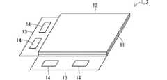
図1は、実施の形態1の発光ダイオード(LED)ディスプレイを模式的に図示する斜視図である。図2は、実施の形態1のLEDディスプレイに備えられるアレイ基板、周辺回路搭載タブ及び周辺回路集積チップを模式的に図示する平面図である。Embodiment 1
1.1 Outline of LED Display FIG. 1 is a perspective view schematically showing the light emitting diode (LED) display according to the first embodiment. FIG. 2 is a plan view schematically showing an array substrate, a peripheral circuit mounting tab, and a peripheral circuit integrated chip included in the LED display of the first embodiment.
図1に図示される実施の形態1のLEDディスプレイ1は、アレイ基板11、対向基板12、周辺回路搭載タブ13及び周辺回路集積チップ14を備える。 The LED display 1 according to the first embodiment illustrated in FIG. 1 includes an
対向基板12は、アレイ基板11に対向する。周辺回路搭載タブ13は、アレイ基板11に接続される。周辺回路集積チップ14は、周辺回路搭載タブ13上に搭載される。 The
周辺回路集積チップ14は、図示されない集積回路を備える。集積回路は、周辺回路を構成する。周辺回路は、映像信号を発生させる。 The peripheral circuit integrated
周辺回路搭載タブ13は、図示されない配線パターンを備える。配線パターンは、周辺回路に電気的に接続される。配線パターンは、発生させられた映像信号を伝送し、伝送した映像信号をアレイ基板11に供給する。 The peripheral
アレイ基板11は、図2に図示されるように、複数の画素101を備える。複数の画素101は、マトリクス状に配列される。複数の画素101に含まれる各画素は、発光ダイオード(LED)及び薄膜トランジスタ(TFT)を備える。TFTは、供給された映像信号にしたがってLEDを駆動する。これにより、各画素101の発光状態が制御され、供給された映像信号に応じた映像がアレイ基板11に表示される。 The
対向基板12は、図示されないブラックマトリックス、外光反射防止膜等を備える。 The
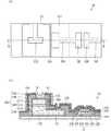
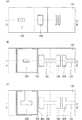
1.2 各画素の構造の概略
図3は、実施の形態1のLEDディスプレイに備えられる各画素を模式的に図示する図である。図3(a)は、平面図である。図3(b)は、断面図である。図3(b)は、図3(a)に描かれた切断線A−Aの位置における断面を図示する。図3においては、下述するエッチングストッパ層、ソース電極、ドレイン電極、ソース配線、ドレイン配線及びコモン配線上に配置される要素の図示が省略されている。例えば、色変換層、上部保護膜、平坦化膜等の要素の図示が省略されている。また、図3においては、複数のTFTを備えLEDに流れる電流を制御する回路の要素のうち、LEDに最近接する回路最終段のTFT以外の要素の図示が省略されている。1.2 Outline of Structure of Each Pixel FIG. 3 is a diagram schematically illustrating each pixel included in the LED display according to the first embodiment. FIG. 3A is a plan view. FIG. 3B is a sectional view. FIG. 3B illustrates a cross section at the position of the cutting line AA drawn in FIG. In FIG. 3, the elements arranged on the etching stopper layer, the source electrode, the drain electrode, the source wiring, the drain wiring, and the common wiring described below are omitted. For example, the illustration of elements such as the color conversion layer, the upper protective film, and the flattening film is omitted. Further, in FIG. 3, among the elements of the circuit which includes a plurality of TFTs and controls the current flowing through the LED, the elements other than the TFT at the final stage of the circuit closest to the LED are not shown.
各画素101は、図3に図示されるように、ガラス基板111、グラフェン層112、バッファ層113、n型窒化ガリウム(GaN)層114、発光層115、p型窒化ガリウム(GaN)層116、第1のパッド電極118、透明導電膜119、第2のパッド電極120、保護膜121、下地膜122、ゲート電極123、遮光膜124、ゲート絶縁膜125、半導体チャネル層126、エッチングストッパ層127、ソース電極128、ドレイン電極129、ソース配線130、ドレイン配線131及びコモン配線132を備える。 Each
n型GaN層114、発光層115及びp型GaN層116は、LED層140を構成する。第1のパッド電極118、透明導電膜119、第2のパッド電極120及びLED層140は、LED150を構成する。LED150は、無機LEDである。 The n-
下地膜122、ゲート電極123、ゲート絶縁膜125、半導体チャネル層126、ソース電極128及びドレイン電極129は、TFT151を構成する。 The
LED150及びTFT151は、ガラス基板111上に配置される。 The
LED層140は、LED150が光を発する際に再結合する電子及び正孔が存在する層である。LED層140は、窒化ガリウム(GaN)系材料又は窒化インジウム(InN)系材料からなる堆積層114,115及び116を備える。堆積層114,115及び116は、望ましくはスパッタリング法、パルスレーザー堆積法等により形成される。 The LED layer 140 is a layer in which electrons and holes are recombined when the
LED層140は、グラフェン層112上に配置される。また、LED層140の最下部層114は、窒化ガリウム(GaN)系材料からなる。この構造によれば、高い結晶性を有するLED層140を得ることができる。この点については、アレイ基板11の製造についての説明の中で再び言及する。 The LED layer 140 is disposed on the
TFT151は、逆スタガ型の構造を有する。TFT151は、LED層140から見て、ガラス基板111の厚さ方向と垂直をなす水平方向に配置される。これにより、TFT151を作製した後にLED150を作製しなければならないという制約が解消し、LED150を作製した後にTFT151を作製することができる。 The
1.3 各画素を構成する要素
ガラス基板111は、ガラス基板111上に配置されるグラフェン層112、バッファ層113、n型GaN層114、発光層115、p型GaN層116、第1のパッド電極118、透明導電膜119、第2のパッド電極120、保護膜121、下地膜122、ゲート電極123、遮光膜124、ゲート絶縁膜125、半導体チャネル層126、エッチングストッパ層127、ソース電極128、ドレイン電極129、ソース配線130、ドレイン配線131及びコモン配線132を支持する。ガラス基板111は、ガラスからなる。ガラス基板111がガラス以外の絶縁体からなる絶縁体基板に置き換えられてもよい。例えば、ガラス基板111がセラミックスからなるセラミックス基板等に置き換えられてもよい。1.3 Elements Constituting Each Pixel The
グラフェン層112は、ガラス基板111上に配置される。グラフェン層112は、グラフェンからなる。グラフェン層112は、結晶格子整合層として機能する。グラフェン層112が、グラフェン以外の六方晶系炭素物質からなる六方晶系炭素物質層に置き換えられてもよい。例えば、グラフェン層112が、グラファイトからなるグラファイト層に置き換えられてもよい。 The
バッファ層113は、グラフェン層112上に配置される。バッファ層113は、望ましくは窒化金属からなり、さらに望ましくは窒化アルミニウム(AlN)からなる。 The
n型GaN層114は、バッファ層113上に配置される。n型GaN層114は、n型GaNからなる。n型GaN層114が、n型GaN以外のn型半導体からなるn型半導体層に置き換えられてもよい。 The n-
発光層115は、n型GaN層114上に配置される。発光層115は、多重量子井戸ダブルへテロ構造を有する。発光層115は、極薄層の積層体及びp型窒化アルミニウムガリウム(AlGaN)層を備える。p型AlGaN層は、極薄層の積層体上に配置される。極薄層の積層体は、6組のペア層を備える。6組のペア層の各々は、n型窒化ガリウム(GaN)層及び窒化インジウムガリウム(InGaN)層を備える。6組のペア層の各々において、InGaN層は、n型GaN層上に配置される。n型GaN層は、n型GaNからなる。InGaN層は、InGaNからなる。InGaNは、窒化インジウム(InN)及び窒化ガリウム(GaN)の複合窒化物である。p型AlGaN層は、p型AlGaNからなる。p型AlGaNは、窒化アルミニウム(AlN)及び窒化ガリウム(GaN)の複合窒化物、並びにそれに添加される極微量のマグネシウム(Mg)からなる。発光層115によれば、LED150の発光効率を向上することができる。発光層115が上述した構造と異なる構造を有する発光層に置き換えられてもよい。 The
p型GaN層116は、発光層115上に配置される。これにより、発光層115は、n型GaN層114とp型GaN層116とに挟まれる。p型GaN層116は、p型GaNからなる。p型GaNは、窒化ガリウム(GaN)及びそれに添加される極微量のマグネシウム(Mg)からなる。p型GaN層116が、p型GaN以外のp型半導体からなるp型半導体層に置き換えられてもよい。 The p-
第1のパッド電極118は、n型GaN層114上に配置される。第1のパッド電極118は、導電体からなり、望ましくは、主に金(Au)及びパラジウム(Pd)からなる金−パラジウム合金からなる。第1のパッド電極118によれば、n型GaN層114をソース電極128に電気的に接続することができ、発光層115からn型GaN層114及び第1のパッド電極118を順次に経由してソース配線130まで電流を安定的に流すことができる。 The
透明導電膜119は、p型GaN層116上に配置される。透明導電膜119は、p型GaN層116の上面の全面を覆う。透明導電膜119は、わずかな厚さしか有しない。透明導電膜119は、導電体からなり、望ましくは、パラジウム(Pd)合金からなる。透明導電膜119によれば、p型GaN層116を経由して発光層115に均一に電流を流することができ、LED150の発光ムラを抑制することができる。 The transparent
第2のパッド電極120は、透明導電膜119上に配置される。第2のパッド電極120は、導電体からなり、望ましくは、主に金(Au)及びパラジウム(Pd)からなる金−パラジウム合金からなる。第2のパッド電極120によれば、透明導電膜119がわずかな厚さしか有しない場合であっても、p型GaN層116及び透明導電膜119をコモン配線132に電気的に接続することができ、コモン配線132から第2のパッド電極120、透明導電膜119及びp型GaN層116を順次に経由して発光層115まで電流を安定的に流すことができる。 The
保護膜121は、第1のパッド電極118及び第2のパッド電極120が配置される部分を除いてLED層140を覆う。保護膜121は、絶縁体からなり、望ましくは、酸化珪素(SiO2)又は窒化珪素(Si3N4)からなる。保護膜121は、パッシベーション膜等とも呼ばれる。保護膜121は、単層膜及び多層膜のいずれであってもよい。多層膜は、酸化珪素からなる膜、及び窒化珪素からなる膜からなる二層膜等である。保護膜121によれば、汚染物、水分等の外来物に弱いLED層140に外来物が侵入することを阻害することができ、LED層140が外来物により劣化することを抑制することができる。The
下地膜122は、ガラス基板111上に配置される。下地膜122は、絶縁体からなり、望ましくは、酸化珪素(SiO2)又は窒化珪素(Si3N4)からなる。下地膜122は、単層膜及び多層膜のいずれであってもよい。多層膜は、酸化珪素からなる膜、及び窒化珪素からなる膜からなる二層膜等である。The
保護膜121及び下地膜122は、同じ材料により構成される。また、保護膜121及び下地膜122は、同じ層に配置される。これにより、保護膜121及び下地膜122を同時に形成することができ、LEDディスプレイ1の生産性を向上することができる。保護膜121及び下地膜122が同じ層に配置されるため、保護膜121と下地膜122との間には他の層は挟まれない。また、保護膜121及び下地膜122の一方は、保護膜121及び下地膜122の他方から連続する。また、保護膜121及び下地膜122は、共通の隣接層であるゲート絶縁膜125に接触する。 The
ゲート電極123は、下地膜122上に配置される。ゲート電極123は、ガラス基板111の厚さ方向から平面視された場合に、半導体チャネル層126の全体に重なり、半導体チャネル層126より大きい。ゲート電極123は、導電体からなり、望ましくは、アルミニウム(Al)合金からなる。アルミニウム合金は、アルミニウム及びそれに添加される極微量のアルミニウム以外の元素からなる。ゲート電極123によれば、LED層140により発せられガラス基板111に反射され半導体チャネル層126に向かう迷光がゲート電極123により遮光される。 The
遮光膜124は、LED層140の側面140s上に配置される。遮光膜124は、導電体からなり、望ましくは、金属又は合金からなり、さらに望ましくは、アルミニウム(Al)合金からなる。アルミニウム合金は、アルミニウム及びそれに添加される極微量のアルミニウム以外の元素からなる。遮光膜124によれば、LED層140により発せられLED層140の側面140sから漏洩する光が遮光膜124により遮光される。 The
ゲート電極123及び遮光膜124は、同じ材料により構成される。また、ゲート電極123及び遮光膜124は、同じ層に配置される。これにより、ゲート電極123及び遮光膜124を同時に形成することができ、LEDディスプレイ1の生産性を向上することができる。ゲート電極123及び遮光膜124が同じ層に配置されるため、ゲート電極123と遮光膜124との間には他の層は挟まれない。また、ゲート電極123及び遮光膜124の一方は、ゲート電極123及び遮光膜124の他方から連続する。また、ゲート電極123及び遮光膜124は、共通の層であるゲート絶縁膜125に接触する。 The
ゲート絶縁膜125は、ゲート電極123を覆う。ゲート絶縁膜125は、絶縁体からなり、望ましくは、酸化珪素(SiO2)又は窒化珪素(Si3N4)からなる。ゲート絶縁膜125は、単層膜及び多層膜のいずれであってもよい。多層膜は、酸化珪素からなる膜、及び窒化珪素からなる膜からなる二層膜等である。The
半導体チャネル層126は、ゲート絶縁膜125上に配置され、ゲート絶縁膜125を介してゲート電極123上に配置される。半導体チャネル層126は、半導体からなり、望ましくは、低温ポリシリコン又は金属酸化物からなる。金属酸化物は、インジウム(In)、ガリウム(Ga)及び亜鉛(Zn)の複合酸化物等である。 The
エッチングストッパ層127は、半導体チャネル層126を覆う。エッチングストッパ層127は、絶縁体からなり、望ましくは、酸化珪素(SiO2)又は窒化珪素(Si3N4)からなる。エッチングストッパ層127は、単層膜及び多層膜のいずれであってもよい。多層膜は、酸化珪素からなる膜、及び窒化珪素からなる膜からなる二層膜等である。The
ソース電極128及びドレイン電極129は、半導体チャネル層126上に配置される。ソース電極128及びドレイン電極129は、導電体からなり、望ましくは、モリブデン(Mo)合金からなる。モリブデン合金は、モリブデン及びそれに添加される極微量のモリブデン以外の元素からなる。 The
ソース配線130及びドレイン配線131は、それぞれ、ソース電極128及びドレイン電極129から連続する。これにより、ソース配線130及びドレイン配線131は、それぞれ、ソース電極128及びドレイン電極129に電気的に接続される。ソース配線130の一部は、第1のパッド電極118上に配置され第1のパッド電極118に接触する。これにより、ソース配線130は、第1のパッド電極118に電気的に接続される。ソース配線130及びドレイン配線131は、導電体からなり、望ましくは、モリブデン(Mo)合金からなる。 The
コモン配線132の一部は、第2のパッド電極120上に配置され第2のパッド電極120に接触する。これにより、コモン配線132は、第2のパッド電極120に電気的に接続される。また、第2のパッド電極120にコモン電位が与えられる。 A part of the
アレイ基板11が、コモン配線132を構成する材料と同じ材料により構成されコモン配線132が配置される層と同じ層に配置される回路配線を備えてもよい。当該回路配線は、コモン配線132と同時に形成することができる。 The
1.4 LEDディスプレイの動作
TFT151がLED150を駆動した場合は、コモン配線132、第2のパッド電極120、透明導電膜119、p型GaN層116、発光層115、n型GaN層114、第1のパッド電極118、ソース配線130及びソース電極128を順次に経由して電流が流れる。また、n型GaN層114から発光層115に電子が注入され、p型GaN層116から発光層115に正孔が注入され、発光層115において正孔と電子とが再結合する。これにより、発光層115から可視領域又は紫外領域の光が発せられる。発せられた光は、あらゆる方向に向かう。1.4 Operation of LED Display When the
1.5 LED層により発せられる光の遮光
半導体チャネル層126に光が照射された場合、又は半導体チャネル層126に光が照射され半導体チャネル層126の温度が上昇した場合は、半導体チャネル層126の電気的特性が変化する場合があり、半導体チャネル層126の寿命が短くなる場合がある。1.5 Blocking of Light Emitted by LED Layer When the
しかし、LEDディスプレイ1においては、LED層140により発せられLED層140の側面140sから漏洩する光が遮光膜124により遮光される。また、LED層140により発せられガラス基板111に反射され半導体チャネル層126に向かう迷光がゲート電極123により遮光される。これらにより、LED層140により発せられる光が半導体チャネル層126に照射されることを抑制することができる。これにより、LEDディスプレイ1の長期信頼性及び寿命を向上することができる。 However, in the LED display 1, light emitted by the LED layer 140 and leaking from the
1.6 遮光膜が配置される側面
LED層140は、ガラス基板111の厚さ方向から平面視された場合に4個の辺を有する四角形状の平面形状を有し、4個の辺をそれぞれ構成する4個の側面を有する。また、LEDディスプレイ1においては、4個の側面の全部の上に遮光膜124が形成される。これにより、LED層140の側面140sのほぼ全体が遮光膜124に覆われ、LED層140の側面140sから漏洩する光が効果的に遮光される。このこと、及びゲート電極123が半導体チャネル層126の全体に重なり半導体チャネル層126より大きいことにより、LEDディスプレイ1においては、LED層140により発せられた光が半導体チャネル層126に照射されることをほぼ完全に防ぐことができる。1.6 Side Surface on Which Light-Shielding Film is Arranged The LED layer 140 has a quadrangular planar shape having four sides when viewed in a plan view from the thickness direction of the
LEDディスプレイ1においては、ゲート絶縁膜125及びエッチングストッパ層127により遮光膜124がコモン配線132から隔てられるため、4個の側面の全部の上に遮光膜124が形成された場合であっても、遮光膜124がコモン配線132と導通することなくコモン配線132を引き出すことができる。 In the LED display 1, since the light-shielding
LED層140が四角形状の平面形状以外の多角形状の平面形状を有する場合も含めて一般的に言えば、LED層140は、ガラス基板111の厚さ方向から平面視された場合に複数の辺を有する多角形状の形状を有し、複数の辺をそれぞれ構成する複数の側面を有する。また、遮光膜124は、複数の側面の全部の上に形成される。 Generally speaking, including the case where the LED layer 140 has a polygonal planar shape other than the quadrangular planar shape, the LED layer 140 has a plurality of sides when viewed in plan from the thickness direction of the
1.7 アレイ基板の製造の概略
アレイ基板が製造される際には、LED150が作製された後にTFT151が作製される。これにより、TFT151に備えられる半導体チャネル層126が、LED150に備えられるn型GaN層114、発光層115及びp型GaN層116を形成する際の高温に晒されることを回避することができ、当該高温に耐えることができない半導体チャネル層126が当該高温により劣化することを抑制することができる。1.7 Outline of manufacture of array substrate When the array substrate is manufactured, the
図4、図6及び図8は、実施の形態1のLEDディスプレイの製造の途上で作製されるアレイ基板の中間品を模式的に図示する平面図である。図5、図7及び図9は、実施の形態1のLEDディスプレイの製造の途上で作製されるアレイ基板の中間品を模式的に図示する断面図である。図5、図7及び図9は、図4、図6及び図8に描かれた切断線A−Aの位置における断面を図示する。 FIG. 4, FIG. 6 and FIG. 8 are plan views schematically showing an intermediate product of an array substrate manufactured during the manufacture of the LED display of the first embodiment. 5, 7 and 9 are cross-sectional views schematically showing an intermediate product of an array substrate manufactured during the manufacture of the LED display of the first embodiment. 5, 7, and 9 illustrate cross-sections at the location of the section line AA depicted in FIGS. 4, 6, and 8.
1.7.1 基板の洗浄
アレイ基板11が製造される際には、まず、図5(a)に図示されるガラス基板111が必要に応じて洗浄される。ガラス基板111が洗浄される際には、酸溶液、アルカリ容器、有機溶媒等によりガラス基板111が洗浄される。1.7.1 Cleaning of Substrate When the
1.7.2 グラフェン層の形成
続いて、図5(a)に図示されるグラフェン層112xがガラス基板111上に形成される。1.7.2 Formation of Graphene Layer Subsequently, the
グラフェン層112xがガラス基板111上に形成される際には、グラフェン層112xがニッケル基板上に形成され、ニッケル基板上に形成されたグラフェン層112xがガラス基板111上に転写される。グラフェン層112xは、化学気相成長(CVD)法等によりニッケル基板上に形成される。 When the
グラフェン層112xによれば、グラフェン層112x上に、図5(a)に図示される良好な結晶性を有するバッファ層113xを低温で形成することができる。また、バッファ層113x上に、図5(a)に図示される良好な結晶性を有するn型GaN層114x、発光層115x及びp型GaN層116xを低温で形成することができる。例えば、良好な結晶性を有するn型GaN層114x、発光層115x及びp型GaN層116xをスパッタリング法、パルスレーザー堆積法等により低温で形成することができる。これにより、発光層115xから得られる発光層115にその機能を発揮させるのに必要な結晶性をn型GaN層114x、発光層115x及びp型GaN層116xに付与することができる。 According to the
1.7.3 バッファ層の形成
続いて、図5(a)に図示されるバッファ層113xがグラフェン層112x上に形成される。1.7.3 Formation of Buffer Layer Subsequently, the
バッファ層113xは、有機金属化学気相成長(MOCVD)法、パルスレーザー堆積法、スパッタリング法等により形成される。バッファ層113xが形成される際には、ある程度の結晶の乱れも考慮してバッファ層113xの結晶性が厳密に制御される。形成されるバッファ層113xは、例えば50nmの厚さを有する。 The
バッファ層113xによれば、バッファ層113x上に形成されるn型GaN層114xとの良好な結晶格子整合を実現することができる。 According to the
1.7.4 n型GaN層の形成
続いて、図5(a)に図示されるn型GaN層114xがバッファ層113x上に形成される。1.7.4 Formation of n-type GaN layer Subsequently, the n-type GaN layer 114x illustrated in FIG. 5A is formed on the
n型GaN層114xは、大きな面積を有する層を形成することができる方法で形成される。例えば、n型GaN層114xは、スパッタリング法、パルスレーザー堆積法等により形成される。形成されるn型GaN層114xは、例えば、1000nmの厚さを有する。n型GaN層114xは、望ましくは、ガラス基板111が許容する温度の範囲内で高い温度で形成され、さらに望ましくは、500℃以上で形成される。 The n-type GaN layer 114x is formed by a method capable of forming a layer having a large area. For example, the n-type GaN layer 114x is formed by a sputtering method, a pulse laser deposition method, or the like. The formed n-type GaN layer 114x has a thickness of 1000 nm, for example. The n-type GaN layer 114x is preferably formed at a high temperature within a temperature range allowed by the
1.7.5 発光層の形成
続いて、図5(a)に図示される発光層115xがn型GaN層114x上に形成される。1.7.5 Formation of Light Emitting Layer Subsequently, the
発光層115xが形成される際には、発光層115xを構成するn型GaN層、InGaN層及びp型AlGaN層が大きな面積を有する層を形成することができる方法で形成される。例えば、発光層115xを構成するn型GaN層、InGaN層及びp型AlGaN層がスパッタリング法、パルスレーザー堆積法等により形成される。形成されるn型GaN層は、例えば、13.5nmの厚さを有する。形成されるInGaN層は、例えば、2.5nmの厚さを有する。形成されるp型AlGaN層は、例えば、20nmの厚さを有する。 When the
1.7.6 p型GaN層の形成
続いて、図4(a)及び図5(a)に図示されるp型GaN層116xが発光層115x上に形成される。1.7.6 Formation of p-type GaN layer Subsequently, the p-
p型GaN層116xは、大きな面積を有する層を形成することができる方法で形成される。例えば、p型GaN層116xは、スパッタリング法、パルスレーザー堆積法等により形成される。形成されるp型GaN層116xは、例えば、600nmの厚さを有する。 The p-
p型GaN層116xが形成された直後においては、図4(a)及び図5(a)に図示されるように、グラフェン層112x、バッファ層113x、n型GaN層114x及びp型GaN層116xが各画素101の全面に渡って配置されており、TFT151を形成することができる場所が存在しない。 Immediately after the p-
1.7.7 グラフェン層、バッファ層、n型GaN層、発光層及びp型GaN層のパターニング
続いて、図4(b)及び図5(b)に図示されるように、グラフェン層112x、バッファ層113x、n型GaN層114x、発光層115x及びp型GaN層116xがパターニングされる。これにより、パターニングされたグラフェン層112、バッファ層113、n型GaN層114y、発光層115y及びp型GaN層116yが形成される。また、TFT151を形成することができる場所が確保される。1.7.7 Patterning of graphene layer, buffer layer, n-type GaN layer, light-emitting layer and p-type GaN layer Next, as shown in FIGS. 4B and 5B, the
グラフェン層112x、バッファ層113x、n型GaN層114x、発光層115x及びp型GaN層116xがパターニングされる際には、レジストが塗布されてレジスト膜が形成され、形成されたレジスト膜に対して写真製版プロセスが実行されてレジストマスクが形成される。続いて、形成されたレジストマスクを用いてグラフェン層112x、バッファ層113x、n型GaN層114x、発光層115x及びp型GaN層116xがエッチングされる。グラフェン層112x、バッファ層113x、n型GaN層114x、発光層115x及びp型GaN層116xは、リアクティブイオンエッチング等によりエッチングされる。グラフェン層112x、バッファ層113x、n型GaN層114x、発光層115x及びp型GaN層116xがリアクティブイオンエッチングによりエッチングされる際には、塩素系ガス等がエッチングガスとして用いられる。また、ガラス基板111へのダメージを最小限に抑制するために、エッチング時間が精密に制御される。続いて、レジストマスクが除去される。レジストマスクが除去される際には、中間品を酸素プラズマに暴露させるアッシング処理、中間品をレジスト剥離液に浸漬するレジスト剥離等が行われる。続いて、中間品が必要に応じて洗浄される。 When the
グラフェン層112x、バッファ層113x、n型GaN層114x、発光層115x及びp型GaN層116xがパターニングされた直後においては、図4(b)及び図5(b)に図示されるように、n型GaN層114yの上面の全面が発光層115y及びp型GaN層116yに覆われている。このため、第1のパッド電極118を形成することができる場所が存在しない。 Immediately after the
1.7.8 発光層及びp型GaN層のパターニング、並びにn型GaN層の上部の除去
続いて、図4(c)及び図5(c)に図示されるように、発光層115y及びp型GaN層116yがさらにパターニングされる。また、n型GaN層114yの上部が除去される。これにより、発光層115、p型GaN層116及びn型GaN層114が形成される。また、n型GaN層114の上面の一部が露出させられ、第1のパッド電極118を形成することができる場所が確保される。1.7.8 Patterning of Light Emitting Layer and p-type GaN Layer, and Removal of Top of n-type GaN Layer Subsequently, as shown in FIGS. 4(c) and 5(c), the light emitting layers 115y and 115y are formed. The
発光層115y及びp型GaN層116yがパターニングされる際には、発光層115y及びp型GaN層116yが完全にエッチングされる。また、n型GaN層114yの上部が除去される際には、n型GaN層114yがハーフエッチングされる。n型GaN層114yがハーフエッチングされる際には、レジストが塗布されてレジスト膜が形成され、形成されたレジスト膜に対して写真製版プロセスが実行されてレジストマスクが形成される。続いて、レジストマスクを用いてn型GaN層114yの上部がエッチングされる。n型GaN層114yの上部は、リアクティブイオンエッチング等によりエッチングされる。n型GaN層114yの上部がリアクティブイオンエッチングによりエッチングされる際には、塩素系ガス等がエッチングガスとして用いられる。続いて、レジストマスクが除去される。レジストマスクが除去される際には、中間品を酸素プラズマに暴露させるアッシング処理、中間品をレジスト剥離液に浸漬するレジスト剥離等が行われる。続いて、中間品が必要に応じて洗浄される。n型GaN層114のハーフエッチングされた部分は、例えば、400nmの厚さを有する。 When the light emitting layer 115y and the p-
1.7.9 透明導電膜の形成
続いて、図4(d)及び図5(d)に図示されるように、透明導電膜119がp型GaN層116上に形成される。1.7.9 Formation of Transparent Conductive Film Subsequently, as shown in FIGS. 4D and 5D, the transparent
透明導電膜119が形成される際には、各画素101の全面に渡る透明導電膜が形成され、形成された透明導電膜がパターニングされる。 When the transparent
透明導電膜は、スパッタリング法等により形成される。透明導電膜がスパッタリング法により形成される際には、アルゴン(Ar)ガス等がスパッタリングガスとして用いられる。また、中間品が、例えば、150℃に加熱される。形成される透明導電膜は、例えば、3nmの厚さを有する。 The transparent conductive film is formed by a sputtering method or the like. When the transparent conductive film is formed by the sputtering method, argon (Ar) gas or the like is used as the sputtering gas. Further, the intermediate product is heated to, for example, 150°C. The formed transparent conductive film has a thickness of 3 nm, for example.
透明導電膜がパターニングされる際には、レジストが塗布されてレジスト膜が形成され、形成されたレジスト膜に対して写真製版プロセスが実行されてレジストマスクが形成される。続いて、レジストマスクを用いて透明導電膜がエッチングされる。透明導電膜は、ウエットエッチング等によりエッチングされる。続いて、レジストマスクが除去される。レジストマスクが除去される際には、中間品を酸素プラズマに暴露させるアッシング処理、中間品をレジスト剥離液に浸漬するレジスト剥離等が行われる。 When the transparent conductive film is patterned, a resist is applied to form a resist film, and a photolithography process is performed on the formed resist film to form a resist mask. Then, the transparent conductive film is etched using the resist mask. The transparent conductive film is etched by wet etching or the like. Then, the resist mask is removed. When the resist mask is removed, an ashing process for exposing the intermediate product to oxygen plasma, a resist stripping process for immersing the intermediate product in a resist stripping solution, and the like are performed.
1.7.10 第1のパッド電極及び第2のパッド電極の形成
続いて、図6(a)及び図7(a)に図示されるように、第1のパッド電極118がn型GaN層114上に形成される。また、第2のパッド電極120が透明導電膜119上に形成される。第1のパッド電極118及び第2のパッド電極120が形成される際には、各画素101の全面に渡る導電膜が形成され、形成された導電膜がパターニングされる。1.7.10 Formation of First Pad Electrode and Second Pad Electrode Subsequently, as shown in FIGS. 6A and 7A, the
導電膜は、スパッタリング法等により形成される。導電膜がスパッタリング法により形成される際には、アルゴン(Ar)ガス等がスパッタリングガスとして用いられる。また、中間品が、例えば、150℃に加熱される。形成される導電膜は、例えば、15nmの厚さを有する。 The conductive film is formed by a sputtering method or the like. When the conductive film is formed by the sputtering method, argon (Ar) gas or the like is used as the sputtering gas. Further, the intermediate product is heated to, for example, 150°C. The formed conductive film has a thickness of 15 nm, for example.
導電膜がパターニングされる際には、レジストが塗布されてレジスト膜が形成され、形成されたレジスト膜に対して写真製版プロセスが実行されてレジストマスクが形成される。続いて、レジストマスクを用いて導電膜がエッチングされる。導電膜は、ウエットエッチング等によりエッチングされる。続いて、レジストマスクが除去される。レジストマスクが除去される際には、中間品を酸素プラズマに暴露させるアッシング処理、中間品をレジスト剥離液に浸漬するレジスト剥離等が行われる。 When the conductive film is patterned, a resist is applied to form a resist film, and a photolithography process is performed on the formed resist film to form a resist mask. Then, the conductive film is etched using the resist mask. The conductive film is etched by wet etching or the like. Then, the resist mask is removed. When the resist mask is removed, an ashing process for exposing the intermediate product to oxygen plasma, a resist stripping process for immersing the intermediate product in a resist stripping solution, and the like are performed.
1.7.11 保護膜及び下地膜の形成
続いて、図6(b)及び図7(b)に図示されるように、保護膜121がLED層140に重ねて形成される。また、下地膜122がガラス基板111上に形成される。保護膜121及び下地膜122が形成される際には、各画素101の全面に渡る絶縁膜が形成され、形成された絶縁膜がパターニングされる。絶縁膜がパターニングされることにより、第1のパッド電極118及び第2のパッド電極120を露出させる開口が絶縁膜に形成される。1.7.11 Formation of Protective Film and Base Film Subsequently, as shown in FIGS. 6B and 7B, the
絶縁膜は、プラズマCVD法等により形成される。絶縁膜が酸化珪素(SiO2)からなり絶縁膜がプラズマCVD法により形成される際には、シラン(SiH4)ガス及び一酸化二窒素(N2О)ガスからなる混合ガス等が原料ガスとして用いられる。また、中間品が、例えば、300℃に加熱される。形成される絶縁膜は、例えば、400nmの厚さを有する。The insulating film is formed by the plasma CVD method or the like. When the insulating film is formed of silicon oxide (SiO2 ) and the insulating film is formed by the plasma CVD method, a mixed gas of silane (SiH4 ) gas and dinitrogen monoxide (N2 O) gas is used as a source gas. Used as. Further, the intermediate product is heated to, for example, 300°C. The formed insulating film has a thickness of 400 nm, for example.
絶縁膜がパターニングされる際には、レジストが塗布されてレジスト膜が形成され、形成されたレジスト膜に対して写真製版プロセスが実行されてレジストマスクが形成される。続いて、レジストマスクを用いて絶縁膜がエッチングされる。絶縁膜は、リアクティブイオンエッチング等によりエッチングされる。絶縁膜がリアクティブイオンエッチングによりエッチングされる際には、三弗化メタン(CHF3)ガス及び酸素(O2)ガスからなる混合ガス等がエッチングガスとして用いられる。続いて、レジストマスクが除去される。レジストマスクが除去される際には、中間品を酸素プラズマに暴露させるアッシング処理、中間品をレジスト剥離液に浸漬するレジスト剥離等が行われる。続いて、中間品が必要に応じて洗浄される。When the insulating film is patterned, a resist is applied to form a resist film, and a photolithography process is performed on the formed resist film to form a resist mask. Then, the insulating film is etched using the resist mask. The insulating film is etched by reactive ion etching or the like. When the insulating film is etched by reactive ion etching, a mixed gas of methane trifluoride (CHF3 ) gas and oxygen (O2 ) gas is used as an etching gas. Then, the resist mask is removed. When the resist mask is removed, an ashing process for exposing the intermediate product to oxygen plasma, a resist stripping process for immersing the intermediate product in a resist stripping solution, and the like are performed. Subsequently, the intermediate product is washed if necessary.
1.7.12 ゲート電極及び遮光膜の形成
続いて、図6(c)及び図7(c)に図示されるように、ゲート電極123が下地膜122上に形成され、遮光膜124がLED層140の側面140s上に形成される。1.7.12 Formation of Gate Electrode and Light Shielding Film Subsequently, as illustrated in FIGS. 6C and 7C, the
ゲート電極123及び遮光膜124が形成される際には、各画素101の全面に渡る導電膜が形成され、形成された導電膜がパターニングされる。 When the
導電膜は、スパッタリング法等により形成される。導電膜がスパッタリング法により形成される際には、アルゴン(Ar)ガス等がスパッタリングガスとして用いられる。また、中間品が、例えば、150℃に加熱される。形成される導電膜は、例えば、200nmの厚さを有する。 The conductive film is formed by a sputtering method or the like. When the conductive film is formed by the sputtering method, argon (Ar) gas or the like is used as the sputtering gas. Further, the intermediate product is heated to, for example, 150°C. The formed conductive film has a thickness of 200 nm, for example.
導電膜がパターニングされる際には、レジストが塗布されてレジスト膜が形成され、形成されたレジスト膜に対して写真製版プロセスが実行されてレジストマスクが形成される。続いて、レジストマスクを用いて導電膜がエッチングされる。導電膜は、ウエットエッチング等によりエッチングされる。導電膜がウエットエッチングによりエッチングされる際には、リン酸(Phosphoric acid)、硝酸(Acetic acid)及び酢酸(Nitric acid)を含む溶液がエッチング溶液として用いられる。当該溶液は、PAN溶液とも呼ばれる。続いて、レジストマスクが除去される。レジストマスクが除去される際には、中間品を酸素プラズマに暴露させるアッシング処理、中間品をレジスト剥離液に浸漬するレジスト剥離等が行われる。続いて、中間品が必要に応じて洗浄される。 When the conductive film is patterned, a resist is applied to form a resist film, and a photolithography process is performed on the formed resist film to form a resist mask. Then, the conductive film is etched using the resist mask. The conductive film is etched by wet etching or the like. When the conductive film is etched by wet etching, a solution containing phosphoric acid (Phosphoric acid), nitric acid (Acetic acid) and acetic acid (Nitric acid) is used as an etching solution. The solution is also called a PAN solution. Then, the resist mask is removed. When the resist mask is removed, an ashing process for exposing the intermediate product to oxygen plasma, a resist stripping process for immersing the intermediate product in a resist stripping solution, and the like are performed. Subsequently, the intermediate product is washed if necessary.
遮光膜124は、図6(c)に図示されるように、LED層140の側面140sを構成する4個の側面の全部の上に配置される。 As shown in FIG. 6C, the
1.7.13 ゲート絶縁膜の形成
続いて、図6(d)及び図7(d)に図示されるように、ゲート絶縁膜125がゲート電極123に重ねて形成される。1.7.13 Formation of Gate Insulating Film Subsequently, as shown in FIGS. 6D and 7D, the
ゲート絶縁膜125が形成される際には、各画素101の全面に渡る絶縁膜が形成され、形成された絶縁膜がパターニングされる。絶縁膜がパターニングされることにより、第1のパッド電極118及び第2のパッド電極120を露出させる開口が絶縁膜に形成される。 When the
絶縁膜は、プラズマCVD法等により形成される。絶縁膜が酸化珪素(SiO2)からなり絶縁膜がプラズマCVD法により形成される際には、シラン(SiH4)ガス及び一酸化二窒素(N2О)ガスからなる混合ガス等が原料ガスとして用いられる。また、中間品が、例えば、300℃に加熱される。形成される絶縁膜は、例えば、200nmの厚さを有する。The insulating film is formed by the plasma CVD method or the like. When the insulating film is formed of silicon oxide (SiO2 ) and the insulating film is formed by the plasma CVD method, a mixed gas of silane (SiH4 ) gas and dinitrogen monoxide (N2 O) gas is used as a source gas. Used as. Further, the intermediate product is heated to, for example, 300°C. The formed insulating film has a thickness of 200 nm, for example.
絶縁膜がパターニングされる際には、レジストが塗布されてレジスト膜が形成され、形成されたレジスト膜に対して写真製版プロセスが実行されてレジストマスクが形成される。続いて、レジストマスクを用いて絶縁膜がエッチングされる。絶縁膜は、リアクティブイオンエッチング等によりエッチングされる。絶縁膜がリアクティブイオンエッチングによりエッチングされる際には、三弗化メタン(CHF3)ガス及び酸素(O2)ガスからなる混合ガス等がエッチングガスとして用いられる。続いて、レジストマスクが除去される。レジストマスクが除去される際には、中間品を酸素プラズマに暴露させるアッシング処理、中間品をレジスト剥離液に浸漬するレジスト剥離等が行われる。続いて、中間品が必要に応じて洗浄される。When the insulating film is patterned, a resist is applied to form a resist film, and a photolithography process is performed on the formed resist film to form a resist mask. Then, the insulating film is etched using the resist mask. The insulating film is etched by reactive ion etching or the like. When the insulating film is etched by reactive ion etching, a mixed gas of methane trifluoride (CHF3 ) gas and oxygen (O2 ) gas is used as an etching gas. Then, the resist mask is removed. When the resist mask is removed, an ashing process for exposing the intermediate product to oxygen plasma, a resist stripping process for immersing the intermediate product in a resist stripping solution, and the like are performed. Subsequently, the intermediate product is washed if necessary.
1.7.14 半導体チャネル層の形成
続いて、図8(a)及び図9(a)に図示されるように、半導体チャネル層126がゲート絶縁膜125上に形成される。1.7.14 Formation of Semiconductor Channel Layer Subsequently, as shown in FIGS. 8A and 9A, the
半導体チャネル層126が形成される際には、各画素101の全面に渡る半導体膜が形成され、形成された半導体膜がパターニングされる。 When the
半導体膜は、スパッタリング法等により形成される。半導体膜がスパッタリング法により形成され半導体チャネル層126がインジウム(In)、ガリウム(Ga)及び亜鉛(Zn)の複合酸化物からなる場合は、InGaZnOターゲット等がスパッタリングターゲットとして用いられる。InGaZnOターゲットは、例えば、組成式In2O3・Ga2O3・(ZnO)2により表される組成を有するスパッタリングターゲットである。InGaZnOターゲットにおけるインジウム(In)、ガリウム(Ga)、亜鉛(Zn)及び酸素(O)の原子組成比In:Ga:Zn:Oは、例えば、1:1:1:4である。また、半導体膜がスパッタリング法により形成される場合は、アルゴン(Ar)ガス及び酸素(O2)ガスからなる混合ガス等がスパッタリングガスとして用いられる。アルゴンガス及び酸素ガスからなる混合ガスにおけるアルゴンガスの分圧と酸素ガスの分圧との分圧比は、例えば、100:10である。また、半導体膜がスパッタリング法により形成される場合は、中間品が、例えば、250℃に加熱される。形成される半導体層は、例えば、40nmの厚さを有する。The semiconductor film is formed by a sputtering method or the like. In the case where the semiconductor film is formed by a sputtering method and the
半導体膜がパターニングされる際には、レジストが塗布されてレジスト膜が形成され、形成されたレジスト膜に対して写真製版プロセスが実行されてレジストマスクが形成される。続いて、レジストマスクを用いて半導体膜がエッチングされる。半導体膜がエッチングされる際には、半導体膜がウエットエッチングされる。半導体膜がウエットエッチングされる際には、水及び5重量%のシュウ酸を含むシュウ酸系溶液等がエッチング溶液として用いられる。続いて、レジストマスクが除去される。レジストマスクが除去される際には、中間品を酸素プラズマに暴露させるアッシング処理、中間品をレジスト剥離液に浸漬するレジスト剥離等が行われる。続いて、中間品が必要に応じて洗浄される。 When the semiconductor film is patterned, a resist is applied to form a resist film, and a photolithography process is performed on the formed resist film to form a resist mask. Then, the semiconductor film is etched using the resist mask. When the semiconductor film is etched, the semiconductor film is wet-etched. When the semiconductor film is wet-etched, an oxalic acid-based solution containing water and 5% by weight of oxalic acid is used as an etching solution. Then, the resist mask is removed. When the resist mask is removed, an ashing process for exposing the intermediate product to oxygen plasma, a resist stripping process for immersing the intermediate product in a resist stripping solution, and the like are performed. Subsequently, the intermediate product is washed if necessary.
図8(a)及び図9(a)に図示されるように、ゲート電極123は、ガラス基板111の厚さ方向から平面視された場合に、半導体チャネル層126の全体に重なり、半導体チャネル層126より大きい。これにより、LED層140により発せられガラス基板111に反射されゲート電極123上に配置される半導体チャネル層126に向かう迷光がゲート電極123により遮光される。 As illustrated in FIGS. 8A and 9A, the
1.7.15 エッチングストッパ層の形成
続いて、図8(b)及び図9(b)に図示されるように、エッチングストッパ層127が半導体チャネル層126に重ねて形成される。1.7.15 Formation of Etching Stopper Layer Subsequently, as shown in FIGS. 8B and 9B, an
エッチングストッパ層127が形成される際には、各画素101の全面に渡る絶縁膜が形成され、形成された絶縁膜がパターニングされる。絶縁膜がパターニングされることにより、第1のパッド電極118の、ソース配線130が接続される部分、第2のパッド電極120の、コモン配線132が接続される部分、並びに半導体チャネル層126の、ドレイン電極129及びソース電極128が接続される部分を露出させる開口が絶縁膜に形成される。 When the
絶縁膜は、プラズマCVD法等により形成される。絶縁膜が酸化珪素(SiO2)からなり絶縁膜がプラズマCVD法により形成される際には、シラン(SiH4)ガス及び一酸化二窒素(N2О)ガスからなる混合ガス等が原料ガスとして用いられる。また、中間品が、例えば、300℃に加熱される。形成される絶縁膜は、例えば、200nmの厚さを有する。The insulating film is formed by the plasma CVD method or the like. When the insulating film is formed of silicon oxide (SiO2 ) and the insulating film is formed by the plasma CVD method, a mixed gas of silane (SiH4 ) gas and dinitrogen monoxide (N2 O) gas is used as a source gas. Used as. Further, the intermediate product is heated to, for example, 300°C. The formed insulating film has a thickness of 200 nm, for example.
絶縁膜がパターニングされる際には、レジストが塗布されてレジスト膜が形成され、形成されたレジスト膜に対して写真製版プロセスが実行されてレジストマスクが形成される。続いて、レジストマスクを用いて絶縁膜がエッチングされる。絶縁膜は、リアクティブイオンエッチング等によりエッチングされる。絶縁膜がリアクティブイオンエッチングによりエッチングされる際には、三弗化メタン(CHF3)ガス及び酸素(O2)ガスからなる混合ガス等がエッチングガスとして用いられる。続いて、レジストマスクが除去される。レジストマスクが除去される際には、中間品を酸素プラズマに暴露させるアッシング処理、中間品をレジスト剥離液に浸漬するレジスト剥離等が行われる。続いて、中間品が必要に応じて洗浄される。When the insulating film is patterned, a resist is applied to form a resist film, and a photolithography process is performed on the formed resist film to form a resist mask. Then, the insulating film is etched using the resist mask. The insulating film is etched by reactive ion etching or the like. When the insulating film is etched by reactive ion etching, a mixed gas of methane trifluoride (CHF3 ) gas and oxygen (O2 ) gas is used as an etching gas. Then, the resist mask is removed. When the resist mask is removed, an ashing process for exposing the intermediate product to oxygen plasma, a resist stripping process for immersing the intermediate product in a resist stripping solution, and the like are performed. Subsequently, the intermediate product is washed if necessary.
エッチングストッパ層127は、ソース電極128、ドレイン電極129、ソース配線130及びドレイン配線131が形成される際に用いられるエッチング溶液が半導体チャネル層126に接触することを抑制するエッチングストッパとなり、当該エッチング溶液により半導体チャネル層126が腐食することを抑制することに寄与する。 The
1.7.16 ソース電極、ドレイン電極、ソース配線及びドレイン配線の形成
続いて、図8(c)及び図9(c)に図示されるように、ソース電極128、ドレイン電極129、ソース配線130及びドレイン配線131が形成される。1.7.16 Formation of Source Electrode, Drain Electrode, Source Wiring, and Drain Wiring Subsequently, as illustrated in FIGS. 8C and 9C, the
ソース電極128、ドレイン電極129、ソース配線130及びドレイン配線131が形成される際には、各画素101の全面に渡る導電膜が形成され、形成された導電膜がパターニングされる。 When the
導電膜は、スパッタリング法等により形成される。形成される導電膜は、例えば、200nmの厚さを有する。 The conductive film is formed by a sputtering method or the like. The formed conductive film has a thickness of 200 nm, for example.
導電膜がパターニングされる際には、レジストが塗布されてレジスト膜が形成され、形成されたレジスト膜に対して写真製版プロセスが実行されてレジストマスクが形成される。続いて、レジストマスクを用いて導電膜がエッチングされる。導電膜は、ウエットエッチング等によりエッチングされる。導電膜がウエットエッチングによりエッチングされる際には、PAN溶液がエッチング溶液として用いられる。続いて、レジストマスクが除去される。レジストマスクが除去される際には、中間品を酸素プラズマに暴露させるアッシング処理、中間品をレジスト剥離液に浸漬するレジスト剥離等が行われる。続いて、中間品が必要に応じて洗浄される。この間、半導体チャネル層126は、エッチングストッパ層127によりPAN溶液及びレジスト剥離液から保護される。 When the conductive film is patterned, a resist is applied to form a resist film, and a photolithography process is performed on the formed resist film to form a resist mask. Then, the conductive film is etched using the resist mask. The conductive film is etched by wet etching or the like. When the conductive film is etched by wet etching, the PAN solution is used as the etching solution. Then, the resist mask is removed. When the resist mask is removed, an ashing process for exposing the intermediate product to oxygen plasma, a resist stripping process for immersing the intermediate product in a resist stripping solution, and the like are performed. Subsequently, the intermediate product is washed if necessary. During this time, the
1.7.17 コモン配線の形成
続いて、図8(d)及び図9(d)に図示されるように、コモン配線132が形成される。1.7.17 Formation of Common Wiring Subsequently, as shown in FIGS. 8D and 9D, the
コモン配線132が形成される際には、各画素101の全面に渡る導電膜が形成され、形成された導電膜がパターニングされる。 When the
導電膜は、スパッタリング法等により形成される。導電膜がスパッタリング法により形成される際には、アルゴン(Ar)ガス等がスパッタリングガスとして用いられる。また、中間品が、例えば、150℃に加熱される。形成される導電膜は、例えば、200nmの厚さを有し、50μΩcm以下の比抵抗値を有し、2×10⁴S/cm以上の導電率を有する。The conductive film is formed by a sputtering method or the like. When the conductive film is formed by the sputtering method, argon (Ar) gas or the like is used as the sputtering gas. Further, the intermediate product is heated to, for example, 150°C. The formed conductive film has a thickness of, for example, 200 nm, a specific resistance value of 50 μΩcm or less, and a conductivity of 2×10⁴ S/cm or more.
導電膜がパターニングされる際には、レジストが塗布されてレジスト膜が形成され、形成されたレジスト膜に対して写真製版プロセスが実行されてレジストマスクが形成される。続いて、レジストマスクを用いて導電膜がエッチングされる。導電膜は、ウエットエッチング等によりエッチングされる。導電膜がウエットエッチングによりエッチングされる際には、PAN溶液がエッチング溶液として用いられる。続いて、レジストマスクが除去される。レジストマスクが除去される際には、中間品を酸素プラズマに暴露させるアッシング処理、中間品をレジスト剥離液に浸漬するレジスト剥離等が行われる。続いて、中間品が必要に応じて洗浄される。 When the conductive film is patterned, a resist is applied to form a resist film, and a photolithography process is performed on the formed resist film to form a resist mask. Then, the conductive film is etched using the resist mask. The conductive film is etched by wet etching or the like. When the conductive film is etched by wet etching, the PAN solution is used as the etching solution. Then, the resist mask is removed. When the resist mask is removed, an ashing process for exposing the intermediate product to oxygen plasma, a resist stripping process for immersing the intermediate product in a resist stripping solution, and the like are performed. Subsequently, the intermediate product is washed if necessary.
コモン配線132が形成されるのと同時に、コモン配線132以外の回路配線が形成されてもよい。ドレイン電極129の上に、低い電気抵抗を有する材料からなる回路配線及びTFT151以外のTFTにより回路が形成されてもよい。コモン配線132が形成されるのと同時に、複数のTFTにそれぞれ備えられる複数のソースを互いに電気的に接続する配線、複数のTFTにそれぞれ備えられる複数のドレインを互いに電気的に接続する配線等が形成されてもよい。 At the same time that the
1.7.18 アレイ基板の完成
上述した工程の後に、色変換層、上部保護膜、平坦化膜等の要素が必要に応じて形成され、アレイ基板11が完成させられる。1.7.18 Completion of Array Substrate After the steps described above, elements such as a color conversion layer, an upper protective film, and a flattening film are formed as needed, and the
2 実施の形態2
図1は、実施の形態2のLEDディスプレイを模式的に図示する斜視図でもある。図2は、実施の形態2のLEDディスプレイに備えられるアレイ基板、周辺回路搭載タブ及び周辺回路集積チップを模式的に図示する平面図でもある。Second Embodiment
FIG. 1 is also a perspective view schematically illustrating the LED display according to the second embodiment. FIG. 2 is also a plan view schematically showing an array substrate, a peripheral circuit mounting tab, and a peripheral circuit integrated chip included in the LED display according to the second embodiment.
図10は、実施の形態2のLEDディスプレイに備えられる各画素を模式的に図示する図である。図10(a)は、平面図である。図10(b)は、断面図である。図10(b)は、図10(a)に描かれた切断線B−Bの位置における断面を図示する。 FIG. 10 is a diagram schematically illustrating each pixel included in the LED display according to the second embodiment. FIG. 10A is a plan view. FIG.10(b) is sectional drawing. FIG. 10B illustrates a cross section at the position of the cutting line BB drawn in FIG.
実施の形態2のLEDディスプレイ2は、実施の形態1のLEDディスプレイ1と主に下記の相違点で相違する。 The LED display 2 of the second embodiment differs from the LED display 1 of the first embodiment mainly in the following differences.
実施の形態1のLEDディスプレイ1においては、ゲート電極123及び遮光膜124が、同じ材料により構成され、同じ層に配置される。これに対して、実施の形態2のLEDディスプレイ2においては、ソース電極128、ソース配線130、ドレイン電極129、ドレイン配線131及び遮光膜124が、同じ材料により構成され、同じ層に配置される。 In the LED display 1 of the first embodiment, the
以下では、上記の相違点に関連して実施の形態2のLEDディスプレイ2において採用される構成が説明される。説明されない点については、実施の形態1のLEDディスプレイ1において採用される構成と同様の構成が実施の形態2のLEDディスプレイ2においても採用される。 Hereinafter, the configuration adopted in the LED display 2 of the second embodiment will be described in relation to the above differences. Regarding the points not described, the same configuration as that adopted in the LED display 1 of the first embodiment is also adopted in the LED display 2 of the second embodiment.
遮光膜124は、LED層140の側面140s上に配置される。遮光膜124は、導電体からなり、望ましくは、金属又は合金からなり、さらに望ましくは、アルミニウム(Al)合金からなる。アルミニウム合金は、アルミニウム及びそれに添加される極微量のアルミニウム以外の元素からなる。遮光膜124によれば、LED層140により発せられLED層140の側面140sから漏洩する光が遮光膜124により遮光される。 The
ソース電極128、ドレイン電極129、ソース配線130、ドレイン配線131及び遮光膜124は、同じ材料により構成される。また、ソース電極128、ドレイン電極129、ソース配線130、ドレイン配線131及び遮光膜124は、同じ層に配置される。これにより、ソース電極128、ドレイン電極129、ソース配線130、ドレイン配線131及び遮光膜124を同時に形成することができ、LEDディスプレイ2の生産性を向上することができる。 The
LED層140は、ガラス基板111の厚さ方向から平面視された場合に4個の辺を有する四角形状の平面形状を有し、4個の辺をそれぞれ構成する4個の側面を有する。また、LEDディスプレイ1においては、4個の側面に含まれる、1個の側面を除く残余の側面の全部の上に遮光膜124が形成される。これにより、LED層140の側面140sの大部分が遮光膜124に覆われ、LED層140の側面140sから漏洩する光が効果的に遮光される。このこと、及びゲート電極123が半導体チャネル層126の全体に重なり半導体チャネル層126より大きいことにより、LEDディスプレイ2においては、LED層140により発せられた光が半導体チャネル層126に照射されることをほぼ完全に防ぐことができる。 The LED layer 140 has a quadrangular planar shape having four sides when viewed in a plan view from the thickness direction of the
4個の側面に含まれる1個の側面の上には、遮光膜124が完全には形成されず、当該1個の側面は、遮光膜124が配置されない領域を有する。当該領域は、コモン配線132の引き出しに用いられる。このようにされるのは、LEDディスプレイ2においては、LEDディスプレイ1と異なり、ゲート絶縁膜125及びエッチングストッパ層127により遮光膜124がコモン配線132から隔てられないためである。 The
半導体チャネル層126が酸化物半導体からなる場合は、酸化物半導体に接触するソース電極128及びドレイン電極129は、酸化物半導体との導通を安定して確保するために、望ましくは、高い耐酸化性を有する安定した合金からなる。ソース電極128及びドレイン電極129が高い耐酸化性を有する安定した合金からなる場合は、遮光膜124、ソース配線130及びドレイン配線131も高い耐酸化性を有する安定した合金からなる。このため、遮光膜124が、使用時に発生しやすい腐食現象等に対して強くなり、遮光膜124の長期信頼性が向上し、遮光膜124の遮光特性を長期間にわたって安定して維持することができる。 When the
図4、図6(a)及び図6(b)は、実施の形態2のLEDディスプレイの製造の途上で作製されるアレイ基板の中間品を模式的に図示する平面図でもある。図5、図7(a)及び図7(b)は、実施の形態2のLEDディスプレイの製造の途上で作製されるアレイ基板の中間品を模式的に図示する断面図でもある。 FIG. 4, FIG. 6A, and FIG. 6B are also plan views schematically showing an intermediate product of the array substrate manufactured during the manufacturing of the LED display according to the second embodiment. FIG. 5, FIG. 7A and FIG. 7B are also cross-sectional views schematically showing an intermediate product of the array substrate manufactured during the manufacture of the LED display according to the second embodiment.
図11、図13及び図15は、実施の形態2のLEDディスプレイの製造の途上で作製されるアレイ基板の中間品を模式的に図示する平面図である。図12、図14及び図16は、実施の形態2のLEDディスプレイの製造の途上で作製されるアレイ基板の中間品を模式的に図示する断面図である。図12、図14及び図16は、図11、図13及び図15に描かれた切断線B−Bの位置における断面を図示する。 11, FIG. 13 and FIG. 15 are plan views schematically showing an intermediate product of an array substrate manufactured in the process of manufacturing the LED display according to the second embodiment. 12, FIG. 14 and FIG. 16 are cross-sectional views schematically showing an intermediate product of an array substrate manufactured in the process of manufacturing the LED display according to the second embodiment. 12, 14 and 16 illustrate cross-sections at the section line B-B depicted in FIGS. 11, 13 and 15.
アレイ基板11が製造される際には、保護膜121及び下地膜122が形成されるのに続いて、図11及び図12に図示されるように、各画素101の全面に渡る導電膜123xが形成される。 When the
導電膜123xは、スパッタリング法等により形成される。導電膜123xがスパッタリング法により形成される際には、アルゴン(Ar)ガス等がスパッタリングガスとして用いられる。また、中間品が、例えば、150℃に加熱される。形成される導電膜は、例えば、200nmの厚さを有する。 The
続いて、図13(a)及び図14(a)に図示されるように、形成された導電膜123xがパターニングされる。これにより、ゲート電極123が形成される。ただし、実施の形態1と異なり、ゲート電極123が形成されるのと同時に遮光膜124は形成されない。 Subsequently, as shown in FIGS. 13A and 14A, the formed
導電膜123xがパターニングされる際には、レジストが塗布されてレジスト膜が形成され、形成されたレジスト膜に対して写真製版プロセスが実行されてレジストマスクが形成される。続いて、レジストマスクを用いて導電膜がエッチングされる。導電膜は、ウエットエッチング等によりエッチングされる。導電膜がウエットエッチングによりエッチングされる際には、PAN溶液がエッチング溶液として用いられる。続いて、レジストマスクが除去される。レジストマスクが除去される際には、中間品を酸素プラズマに暴露させるアッシング処理、中間品をレジスト剥離液に浸漬するレジスト剥離等が行われる。続いて、中間品が必要に応じて洗浄される。 When the
続いて、図13(b)及び図14(b)に図示されるように、ゲート絶縁膜125がゲート電極123に重ねて形成される。 Subsequently, as illustrated in FIGS. 13B and 14B, the
ゲート絶縁膜125が形成される際には、実施の形態1と同様に、各画素101の全面に渡る絶縁膜が形成され、形成された絶縁膜がパターニングされる。絶縁膜がパターニングされることにより、第1のパッド電極118及び第2のパッド電極120を露出させる開口が絶縁膜に形成される。 When the
続いて、図13(c)及び図14(c)に図示されるように、半導体チャネル層126がゲート絶縁膜125上に形成される。 Subsequently, as illustrated in FIGS. 13C and 14C, the
半導体チャネル層126が形成される際には、実施の形態1と同様に、各画素101の全面に渡る半導体膜が形成され、形成された半導体膜がパターニングされる。 When the
続いて、図15(a)及び図16(a)に図示されるように、エッチングストッパ層127が半導体チャネル層126に重ねて形成される。 Subsequently, as shown in FIGS. 15A and 16A, the
エッチングストッパ層127が形成される際には、実施の形態1と同様に、各画素101の全面に渡る絶縁膜が形成され、形成された絶縁膜がパターニングされる。 When the
続いて、図15(b)及び図16(b)に図示されるように、ソース電極128、ドレイン電極129、ソース配線130、ドレイン配線131及び遮光膜124が形成される。 Subsequently, as illustrated in FIGS. 15B and 16B, the
ソース電極128、ドレイン電極129、ソース配線130、ドレイン配線131及び遮光膜124が形成される際には、各画素101の全面に渡る導電膜が形成され、形成された導電膜がパターニングされる。 When the
導電膜は、スパッタリング法等により形成される。導電膜がスパッタリング法により形成される際には、アルゴン(Ar)ガス等がスパッタリングガスとして用いられる。また、導電膜が、例えば、150℃に加熱される。形成される導電膜は、例えば、200nmの厚さを有する単層膜である。 The conductive film is formed by a sputtering method or the like. When the conductive film is formed by the sputtering method, argon (Ar) gas or the like is used as the sputtering gas. Further, the conductive film is heated to 150° C., for example. The formed conductive film is, for example, a single layer film having a thickness of 200 nm.
導電膜がパターニングされる際には、レジストが塗布されてレジスト膜が形成され、形成されたレジスト膜に対して写真製版プロセスが実行されてレジストマスクが形成される。続いて、レジストマスクを用いて導電膜がエッチングされる。導電膜は、ウエットエッチング等によりエッチングされる。導電膜がウエットエッチングによりエッチングされる際には、PAN溶液がエッチング溶液として用いられる。続いて、レジストマスクが除去される。レジストマスクが除去される際には、中間品を酸素プラズマに暴露させるアッシング処理、中間品をレジスト剥離液に浸漬するレジスト剥離等が行われる。続いて、中間品が必要に応じて洗浄される。この間、半導体チャネル層126は、エッチングストッパ層127によりPAN溶液及びレジスト剥離液から保護される。 When the conductive film is patterned, a resist is applied to form a resist film, and a photolithography process is performed on the formed resist film to form a resist mask. Then, the conductive film is etched using the resist mask. The conductive film is etched by wet etching or the like. When the conductive film is etched by wet etching, the PAN solution is used as the etching solution. Then, the resist mask is removed. When the resist mask is removed, an ashing process for exposing the intermediate product to oxygen plasma, a resist stripping process for immersing the intermediate product in a resist stripping solution, and the like are performed. Subsequently, the intermediate product is washed if necessary. During this time, the
遮光膜124は、図6(c)に図示されるように、LED層140の側面140sを構成する4個の側面に含まれる、1個の側面を除く残余の側面の全部の上に遮光膜124が形成される。また、4個の側面に含まれる1個の側面の上には、遮光膜124が完全には形成されず、当該1個の側面は、遮光膜124が配置されない領域を有する。 As shown in FIG. 6C, the light-shielding
続いて、図15(c)及び図16(c)に図示されるように、コモン配線132が形成される。 Subsequently, as shown in FIGS. 15C and 16C, the
コモン配線132が形成される際には、実施の形態1と同様に、各画素101の全面に渡る導電膜が形成され、形成された導電膜がパターニングされる。 When the
上述した工程の後に、色変換層、上部保護膜、平坦化膜等の要素が必要に応じて形成され、アレイ基板11が完成させられる。 After the steps described above, elements such as a color conversion layer, an upper protective film, a flattening film are formed as needed, and the
なお、本発明は、その発明の範囲内において、各実施の形態を自由に組み合わせたり、各実施の形態を適宜、変形、省略することが可能である。 It should be noted that, in the present invention, the respective embodiments can be freely combined, or the respective embodiments can be appropriately modified or omitted within the scope of the invention.
この発明は詳細に説明されたが、上記した説明は、すべての局面において、例示であって、この発明がそれに限定されるものではない。例示されていない無数の変形例が、この発明の範囲から外れることなく想定され得るものと解される。 Although the present invention has been described in detail, the above description is an example in all aspects, and the present invention is not limited thereto. It is understood that innumerable variants not illustrated can be envisaged without departing from the scope of the invention.
1,2 LEDディスプレイ、11 アレイ基板、101 画素、111 ガラス基板、112 グラフェン層、114 n型GaN層、115 発光層、116 p型GaN層、121 保護膜、122 下地膜、123 ゲート電極、124 遮光膜、125 ゲート絶縁膜、126 半導体チャネル層、128 ソース電極、129 ドレイン電極、130 ソース配線、131 ドレイン配線、132 コモン配線、140 LED層、150 LED、151 TFT。 1, 2 LED display, 11 array substrate, 101 pixel, 111 glass substrate, 112 graphene layer, 114 n-type GaN layer, 115 light emitting layer, 116 p-type GaN layer, 121 protective film, 122 base film, 123 gate electrode, 124 Light-shielding film, 125 gate insulating film, 126 semiconductor channel layer, 128 source electrode, 129 drain electrode, 130 source wiring, 131 drain wiring, 132 common wiring, 140 LED layer, 150 LED, 151 TFT.
Claims (23)
Translated fromJapanese前記基板上に配置される薄膜トランジスタと、
前記基板上に配置され側面を有するLED層を備え、前記薄膜トランジスタにより駆動されるLEDと、
前記側面上に配置され、前記側面から漏洩する光を遮る遮光膜と、
を備え、
前記薄膜トランジスタは、
ゲート電極と、
前記ゲート電極上に配置される半導体チャネル層と、
を備え、
前記ゲート電極は、前記基板の厚さ方向から平面視された場合に、前記半導体チャネル層の全体に重なり、前記半導体チャネル層より大きく、
前記遮光膜は、前記ゲート電極を構成する材料と同じ材料により構成され、前記ゲート電極が配置される層と同じ層に配置される
LEDディスプレイ。Board,
A thin film transistor arranged on the substrate;
An LED layer disposed on the substrate and having a side surface, the LED driven by the thin film transistor;
A light-shielding film that is disposed on the side surface and blocks light leaking from the side surface;
Equipped with
The thin film transistor is
A gate electrode,
A semiconductor channel layer disposed on the gate electrode,
Equipped with
The gate electrode overlaps the entire semiconductor channel layer when viewed in a plan view from the thickness direction of the substrate, and is larger than the semiconductor channel layer,
In the LED display, the light-shielding film is made of the same material as that of the gate electrode and is arranged in the same layer as the layer in which the gate electrode is arranged.
前記基板上に配置される薄膜トランジスタと、
前記基板上に配置され前記基板の厚さ方向から平面視された場合に複数の辺を有する多角形状の平面形状を有し前記複数の辺を構成する複数の側面を有するLED層を備え、前記薄膜トランジスタにより駆動されるLEDと、
前記複数の側面の全部の上に配置され、前記複数の側面から漏洩する光を遮る遮光膜と、
を備え、
前記薄膜トランジスタは、
ゲート電極と、
前記ゲート電極上に配置される半導体チャネル層と、
を備え、
前記ゲート電極は、前記基板の厚さ方向から平面視された場合に、前記半導体チャネル層の全体に重なり、前記半導体チャネル層より大きい
LEDディスプレイ。Board,
A thin film transistor arranged on the substrate;
An LED layer having a plurality of side surfaces having a polygonal planar shape having a plurality of sides when viewed in a plan view from a thickness direction of the substrate and arranged on the substrate; An LED driven by a thin film transistor,
A light-shielding film that is disposed on all of the plurality of side surfaces and blocks light leaking from the plurality of side surfaces,
Equipped with
The thin film transistor is
A gate electrode,
A semiconductor channel layer disposed on the gate electrode,
Equipped with
In the LED display, the gate electrode overlaps the entire semiconductor channel layer when viewed in a plan view from the thickness direction of the substrate and is larger than the semiconductor channel layer.
前記基板上に配置される薄膜トランジスタと、
前記基板上に配置され側面を有するLED層を備え、前記薄膜トランジスタにより駆動されるLEDと、
前記側面上に配置され、前記側面から漏洩する光を遮る遮光膜と、
を備え、
前記薄膜トランジスタは、
ゲート電極と、
前記ゲート電極上に配置される半導体チャネル層と、
ソース電極と、
ドレイン電極と、
を備え、
前記ゲート電極は、前記基板の厚さ方向から平面視された場合に、前記半導体チャネル層の全体に重なり、前記半導体チャネル層より大きく、
前記遮光膜は、前記ソース電極及び前記ドレイン電極を構成する材料と同じ材料により構成され、前記ソース電極及び前記ドレイン電極が配置される層と同じ層に配置される
LEDディスプレイ。Board,
A thin film transistor arranged on the substrate;
An LED layer disposed on the substrate and having a side surface, the LED driven by the thin film transistor;
A light-shielding film that is disposed on the side surface and blocks light leaking from the side surface;
Equipped with
The thin film transistor is
A gate electrode,
A semiconductor channel layer disposed on the gate electrode,
A source electrode,
A drain electrode,
Equipped with
The gate electrode overlaps the entire semiconductor channel layer when viewed in a plan view from the thickness direction of the substrate, and is larger than the semiconductor channel layer,
In the LED display, the light shielding film is made of the same material as the material of the source electrode and the drain electrode, and is arranged in the same layer as the layer in which the source electrode and the drain electrode are arranged.
前記基板上に配置される薄膜トランジスタと、
前記基板上に配置され前記基板の厚さ方向から平面視された場合に複数の辺を有する多角形状の平面形状を有し前記複数の辺を構成する複数の側面を有するLED層を備え、前記薄膜トランジスタにより駆動されるLEDと、
前記複数の側面に含まれる、ひとつの側面を除く残余の側面の全部の上に配置され、前記残余の側面から漏洩する光を遮る遮光膜と、
を備え、
前記薄膜トランジスタは、
ゲート電極と、
前記ゲート電極上に配置される半導体チャネル層と、
を備え、
前記ゲート電極は、前記基板の厚さ方向から平面視された場合に、前記半導体チャネル層の全体に重なり、前記半導体チャネル層より大きく、
前記ひとつの側面は、前記遮光膜が配置されない領域を有する
LEDディスプレイ。Board,
A thin film transistor arranged on the substrate;
An LED layer having a plurality of side surfaces having a polygonal planar shape having a plurality of sides when viewed in a plan view from a thickness direction of the substrate and arranged on the substrate; An LED driven by a thin film transistor,
A light-shielding film, which is included in the plurality of side surfaces, is disposed on all of the remaining side surfaces except one side surface, and blocks light leaking from the remaining side surfaces,
Equipped with
The thin film transistor is
A gate electrode,
A semiconductor channel layer disposed on the gate electrode,
Equipped with
The gate electrode overlaps the entire semiconductor channel layer when viewed in a plan view from the thickness direction of the substrate, and is larger than the semiconductor channel layer,
The one side surface is an LED display having a region where the light shielding film is not arranged.
前記基板上に配置される薄膜トランジスタと、
前記基板上に配置され側面を有するLED層を備え、前記薄膜トランジスタにより駆動されるLEDと、
前記側面上に配置され、前記側面から漏洩する光を遮る遮光膜と、
を備え、
前記薄膜トランジスタは、
ゲート電極と、
前記ゲート電極及び前記LED層を覆うゲート絶縁膜と、
前記ゲート絶縁膜を介して前記ゲート電極上に配置される半導体チャネル層と、
を備え、
前記ゲート電極は、前記基板の厚さ方向から平面視された場合に、前記半導体チャネル層の全体に重なり、前記半導体チャネル層より大きい
LEDディスプレイ。Board,
A thin film transistor arranged on the substrate;
An LED layer disposed on the substrate and having a side surface, the LED driven by the thin film transistor;
A light-shielding film that is disposed on the side surface and blocks light leaking from the side surface;
Equipped with
The thin film transistor is
A gate electrode,
A gate insulating film covering the gate electrode and the LED layer,
A semiconductor channel layer disposed on the gate electrode via the gate insulating film,
Equipped with
In the LED display, the gate electrode overlaps the entire semiconductor channel layer when viewed in a plan view from the thickness direction of the substrate and is larger than the semiconductor channel layer.
前記基板上に配置される薄膜トランジスタと、
前記基板上に配置され側面を有するLED層を備え、前記薄膜トランジスタにより駆動されるLEDと、
前記側面上に配置され、前記側面から漏洩する光を遮る遮光膜と、
を備え、
前記薄膜トランジスタは、
下地膜と、
前記下地膜上に配置されるゲート電極と、
前記ゲート電極上に配置される半導体チャネル層と、
を備え、
前記ゲート電極は、前記基板の厚さ方向から平面視された場合に、前記半導体チャネル層の全体に重なり、前記半導体チャネル層より大きく、
前記LED層を覆い、前記下地膜を構成する材料と同じ材料により構成され、前記下地膜が配置される層と同じ層に配置される保護膜をさらに備える
LEDディスプレイ。Board,
A thin film transistor arranged on the substrate;
An LED layer disposed on the substrate and having a side surface, the LED driven by the thin film transistor;
A light-shielding film that is disposed on the side surface and blocks light leaking from the side surface;
Equipped with
The thin film transistor is
A base film,
A gate electrode disposed on the base film,
A semiconductor channel layer disposed on the gate electrode,
Equipped with
The gate electrode overlaps the entire semiconductor channel layer when viewed in a plan view from the thickness direction of the substrate, and is larger than the semiconductor channel layer,
The LED display further comprising a protective film which covers the LED layer and is made of the same material as that of the base film and is disposed in the same layer as the layer in which the base film is disposed.
請求項2、5又は6のLEDディスプレイ。The LED display according to claim 2, 5 or 6, wherein the light-shielding film is made of the same material as that of the gate electrode and is arranged in the same layer as the layer in which the gate electrode is arranged.
前記遮光膜は、前記ソース電極及び前記ドレイン電極を構成する材料と同じ材料により構成され、前記ソース電極及び前記ドレイン電極が配置される層と同じ層に配置される
請求項4、5又は6のLEDディスプレイ。The thin film transistor further includes a source electrode and a drain electrode,
7. The light shielding film is made of the same material as that of the source electrode and the drain electrode, and is arranged in the same layer as the layer in which the source electrode and the drain electrode are arranged. LED display.
前記遮光膜は、前記複数の側面の全部の上に配置される
請求項1、5又は6のLEDディスプレイ。The LED layer has a polygonal planar shape having a plurality of sides when viewed in a plan view from the thickness direction of the substrate, and has a plurality of side surfaces forming the plurality of sides,
The LED display according to claim 1, 5 or 6, wherein the light shielding film is disposed on all of the plurality of side surfaces.
前記遮光膜は、前記複数の側面に含まれる、ひとつの側面を除く残余の側面の全部の上に配置され、
前記ひとつの側面は、前記遮光膜が配置されない領域を有する
請求項3、5又は6のLEDディスプレイ。The LED layer has a polygonal planar shape having a plurality of sides when viewed in a plan view from the thickness direction of the substrate, and has a plurality of side surfaces forming the plurality of sides,
The light-shielding film is disposed on all of the remaining side surfaces included in the plurality of side surfaces except one side surface,
The LED display according to claim 3, 5 or 6, wherein the one side surface has a region where the light shielding film is not arranged.
前記ゲート電極は、前記下地膜上に配置され、
前記LED層を覆い、前記下地膜を構成する材料と同じ材料により構成され、前記下地膜が配置される層と同じ層に配置される保護膜をさらに備える
請求項1から10までのいずれかのLEDディスプレイ。The thin film transistor further includes a base film,
The gate electrode is disposed on the base film,
The protective film which covers the LED layer and is made of the same material as that of the base film and is arranged in the same layer as the layer in which the base film is arranged. LED display.
請求項1から11までのいずれかのLEDディスプレイ。The LED display according to claim 1, further comprising an etching stopper layer that covers the semiconductor channel layer and the LED layer.
請求項1から12までのいずれかのLEDディスプレイ。13. The LED display according to claim 1, wherein the thin film transistor has an inverted staggered structure.
請求項1から13までのいずれかのLEDディスプレイ。The LED display according to any one of claims 1 to 13, wherein the thin film transistor is arranged in a direction perpendicular to a thickness direction of the substrate when viewed from the LED layer.
請求項1から14までのいずれかのLEDディスプレイ。The LED display according to claim 1, wherein the LED layer comprises a deposited layer made of a gallium nitride-based material or an indium nitride-based material.
前記LED層は、前記グラフェン層上に配置され窒化ガリウム系材料からなる最下部層を備える
請求項1から15までのいずれかのLEDディスプレイ。Further comprising a graphene layer,
The LED display according to any one of claims 1 to 15, wherein the LED layer includes a bottom layer formed on the graphene layer and made of a gallium nitride-based material.
請求項1から16までのいずれかのLEDディスプレイ。The LED display according to claim 1, wherein the semiconductor channel layer is made of a metal oxide.
b) 工程a)の後に、前記LEDを駆動する薄膜トランジスタを前記基板上に形成する工程と、
c) 前記側面から漏洩する光を遮る遮光膜を前記側面上に形成する工程と、
を備え、
工程b)は、
b-1) 工程c)と同時に、ゲート電極を前記基板上に形成する工程と、
b-2) 前記基板の厚さ方向から平面視された場合に前記ゲート電極が半導体チャネル層の全体に重なり前記半導体チャネル層より大きくなるように前記半導体チャネル層を前記ゲート電極上に形成する工程と、
を備える
LEDディスプレイの製造方法。a) forming an LED on the substrate comprising an LED layer having side surfaces;
b) after step a), forming a thin film transistor for driving the LED on the substrate,
c) forming a light-shielding film on the side surface that blocks light leaking from the side surface,
Equipped with
Step b) is
b-1) simultaneously with step c), a step of forming a gate electrode on the substrate,
b-2) a step of forming the semiconductor channel layer on the gate electrode so that the gate electrode overlaps the entire semiconductor channel layer and is larger than the semiconductor channel layer when viewed in plan from the thickness direction of the substrate When,
An LED display manufacturing method comprising:
b) 工程a)の後に、前記LEDを駆動する薄膜トランジスタを前記基板上に形成する工程と、
c) 前記複数の側面の全部の上に前記複数の側面から漏洩する光を遮る遮光膜を形成する工程と、
を備え、
工程b)は、
b-1) ゲート電極を前記基板上に形成する工程と、
b-2) 前記基板の厚さ方向から平面視された場合に前記ゲート電極が半導体チャネル層の全体に重なり前記半導体チャネル層より大きくなるように前記半導体チャネル層を前記ゲート電極上に形成する工程と、
を備える
LEDディスプレイの製造方法。a) forming an LED on a substrate having an LED layer having a polygonal planar shape having a plurality of sides when viewed from the thickness direction of the substrate and having a plurality of side surfaces forming the plurality of sides The process of
b) after step a), forming a thin film transistor for driving the LED on the substrate,
c) forming a light-shielding film that blocks light leaking from the plurality of side surfaces on all of the plurality of side surfaces,
Equipped with
Step b) is
b-1) a step of forming a gate electrode on the substrate,
b-2) a step of forming the semiconductor channel layer on the gate electrode so that the gate electrode overlaps the entire semiconductor channel layer and is larger than the semiconductor channel layer when viewed in plan from the thickness direction of the substrate When,
An LED display manufacturing method comprising:
b) 工程a)の後に、前記LEDを駆動する薄膜トランジスタを前記基板上に形成する工程と、
c) 前記側面から漏洩する光を遮る遮光膜を前記側面上に形成する工程と、
を備え、
工程b)は、
b-1) ゲート電極を前記基板上に形成する工程と、
b-2) 前記基板の厚さ方向から平面視された場合に前記ゲート電極が半導体チャネル層の全体に重なり前記半導体チャネル層より大きくなるように前記半導体チャネル層を前記ゲート電極上に形成する工程と、
b-3) 工程c)と同時に、ソース電極及びドレイン電極を前記半導体チャネル層上に形成する工程と、
を備える
LEDディスプレイの製造方法。a) forming an LED on the substrate comprising an LED layer having side surfaces;
b) after step a), forming a thin film transistor for driving the LED on the substrate,
c) forming a light-shielding film on the side surface that blocks light leaking from the side surface,
Equipped with
Step b) is
b-1) a step of forming a gate electrode on the substrate,
b-2) forming the semiconductor channel layer wherein as the gate electrode is larger than the semiconductor channel layer overlaps the entiresemiconductor channel layer when it is viewed from the thickness direction of the substrate on the gate electrode When,
b-3) simultaneously with step c), a step of forming a source electrode and a drain electrode on the semiconductor channel layer,
An LED display manufacturing method comprising:
b) 工程a)の後に、前記LEDを駆動する薄膜トランジスタを前記基板上に形成する工程と、
c) 前記複数の側面に含まれる、ひとつの側面を除く残余の側面の全部の上に、残余の側面から漏洩する光を遮る遮光膜を、前記ひとつの側面が前記遮光膜が配置されない領域を有するように形成する工程と、
を備え、
工程b)は、
b-1) ゲート電極を前記基板上に形成する工程と、
b-2) 前記基板の厚さ方向から平面視された場合に前記ゲート電極が半導体チャネル層の全体に重なり前記半導体チャネル層より大きくなるように前記半導体チャネル層を前記ゲート電極上に形成する工程と、
LEDディスプレイの製造方法。a) forming an LED on a substrate having an LED layer having a polygonal planar shape having a plurality of sides when viewed from the thickness direction of the substrate and having a plurality of side surfaces forming the plurality of sides The process of
b) after step a), forming a thin film transistor for driving the LED on the substrate,
c) A light-shielding film that blocks light leaking from the remaining side surface on all of the remaining side surfaces except one side surface included in the plurality of side surfaces, and the one side surface is a region where the light-shielding film is not disposed. Forming to have
Equipped with
Step b) is
b-1) a step of forming a gate electrode on the substrate,
b-2) forming the semiconductor channel layer wherein as the gate electrode is larger than the semiconductor channel layer overlaps the entiresemiconductor channel layer when it is viewed from the thickness direction of the substrate on the gate electrode When,
Manufacturing method of LED display.
b) 工程a)の後に、前記LEDを駆動する薄膜トランジスタを前記基板上に形成する工程と、
c) 前記側面から漏洩する光を遮る遮光膜を前記側面上に形成する工程と、
を備え、
工程b)は、
b-1) ゲート電極を前記基板上に形成する工程と、
b-2) 前記ゲート電極及び前記LED層に重ねてゲート絶縁膜を形成する工程と、
b-3) 前記基板の厚さ方向から平面視された場合に前記ゲート電極が半導体チャネル層の全体に重なり前記半導体チャネル層より大きくなり前記半導体チャネル層が前記ゲート絶縁膜を介して前記ゲート電極上に配置されるように前記半導体チャネル層を前記ゲート電極上に形成する工程と、
を備える
LEDディスプレイの製造方法。a) forming an LED on the substrate comprising an LED layer having side surfaces;
b) after step a), forming a thin film transistor for driving the LED on the substrate,
c) forming a light-shielding film on the side surface that blocks light leaking from the side surface,
Equipped with
Step b) is
b-1) a step of forming a gate electrode on the substrate,
b-2) a step of forming a gate insulating film on the gate electrode and the LED layer,
b-3) The gate electrode overlaps the entire semiconductor channel layer and is larger than the semiconductor channel layer when viewed in a plan view from the thickness direction of the substrate, and the semiconductor channel layer has the gate electrode via the gate insulating film. Forming the semiconductor channel layer on the gate electrode so as to be disposed above;
An LED display manufacturing method comprising:
b) 工程a)の後に、前記LEDを駆動する薄膜トランジスタを前記基板上に形成する工程と、
c) 前記側面から漏洩する光を遮る遮光膜を前記側面上に形成する工程と、
を備え、
工程b)は、
b-1) 前記LED層に重ねて保護膜を形成し、前記保護膜を形成するのと同時に、下地膜を基板上に形成する工程と、
b-2) 前記下地膜上にゲート電極を前記基板上に形成する工程と、
b-3) 前記基板の厚さ方向から平面視された場合に前記ゲート電極が半導体チャネル層の全体に重なり前記半導体チャネル層より大きくなるように前記半導体チャネル層を前記ゲート電極上に形成する工程と、
を備える
LEDディスプレイの製造方法。a) forming an LED on the substrate comprising an LED layer having side surfaces;
b) after step a), forming a thin film transistor for driving the LED on the substrate,
c) forming a light-shielding film on the side surface that blocks light leaking from the side surface,
Equipped with
Step b) is
b-1) a step of forming a protective film on the LED layer and forming the protective film, and at the same time ,forming a base film on the substrate;
b-2) a step of forming a gate electrode on the substrate on the base film,
b-3) a step of forming the semiconductor channel layer on the gate electrode so that the gate electrode overlaps the entire semiconductor channel layer and is larger than the semiconductor channel layer when viewed in plan from the thickness direction of the substrate When,
An LED display manufacturing method comprising:
Applications Claiming Priority (3)
| Application Number | Priority Date | Filing Date | Title |
|---|---|---|---|
| JP2019048396 | 2019-03-15 | ||
| JP2019048396 | 2019-03-15 | ||
| PCT/JP2019/033459WO2020188851A1 (en) | 2019-03-15 | 2019-08-27 | Led display |
Publications (2)
| Publication Number | Publication Date |
|---|---|
| JP6723484B1true JP6723484B1 (en) | 2020-07-15 |
| JPWO2020188851A1 JPWO2020188851A1 (en) | 2021-04-01 |
Family
ID=71523916
Family Applications (1)
| Application Number | Title | Priority Date | Filing Date |
|---|---|---|---|
| JP2019569976AActiveJP6723484B1 (en) | 2019-03-15 | 2019-08-27 | LED display and method of manufacturing LED display |
Country Status (1)
| Country | Link |
|---|---|
| JP (1) | JP6723484B1 (en) |
Cited By (2)
| Publication number | Priority date | Publication date | Assignee | Title |
|---|---|---|---|---|
| JPWO2024053198A1 (en)* | 2022-09-06 | 2024-03-14 | ||
| JP2024537366A (en)* | 2021-10-19 | 2024-10-10 | 高麗大学校産学協力団 | Light-emitting element-thin film transistor integration structure |
Citations (5)
| Publication number | Priority date | Publication date | Assignee | Title |
|---|---|---|---|---|
| JP2003037268A (en)* | 2001-07-24 | 2003-02-07 | Minolta Co Ltd | Semiconductor device and method of manufacturing the same |
| JP2009141221A (en)* | 2007-12-07 | 2009-06-25 | Sony Corp | METHOD OF MANUFACTURING ZnO SEMICONDUCTOR FILM, ZnO SEMICONDUCTOR FILM, AND SEMICONDUCTOR DEVICE USING THE SAME |
| JP2015015321A (en)* | 2013-07-03 | 2015-01-22 | 高槻電器工業株式会社 | Semiconductor light emitting device and manufacturing method thereof |
| US20170170373A1 (en)* | 2015-12-15 | 2017-06-15 | Innolux Corporation | Light-emitting diode and display device manufactured from the light-emitting diode |
| CN108011012A (en)* | 2017-11-08 | 2018-05-08 | 友达光电股份有限公司 | Element substrate and method for manufacturing the same |
- 2019
- 2019-08-27JPJP2019569976Apatent/JP6723484B1/enactiveActive
Patent Citations (5)
| Publication number | Priority date | Publication date | Assignee | Title |
|---|---|---|---|---|
| JP2003037268A (en)* | 2001-07-24 | 2003-02-07 | Minolta Co Ltd | Semiconductor device and method of manufacturing the same |
| JP2009141221A (en)* | 2007-12-07 | 2009-06-25 | Sony Corp | METHOD OF MANUFACTURING ZnO SEMICONDUCTOR FILM, ZnO SEMICONDUCTOR FILM, AND SEMICONDUCTOR DEVICE USING THE SAME |
| JP2015015321A (en)* | 2013-07-03 | 2015-01-22 | 高槻電器工業株式会社 | Semiconductor light emitting device and manufacturing method thereof |
| US20170170373A1 (en)* | 2015-12-15 | 2017-06-15 | Innolux Corporation | Light-emitting diode and display device manufactured from the light-emitting diode |
| CN108011012A (en)* | 2017-11-08 | 2018-05-08 | 友达光电股份有限公司 | Element substrate and method for manufacturing the same |
Cited By (4)
| Publication number | Priority date | Publication date | Assignee | Title |
|---|---|---|---|---|
| JP2024537366A (en)* | 2021-10-19 | 2024-10-10 | 高麗大学校産学協力団 | Light-emitting element-thin film transistor integration structure |
| JP7716801B2 (en) | 2021-10-19 | 2025-08-01 | 高麗大学校産学協力団 | Light-emitting element-thin film transistor integration structure |
| JPWO2024053198A1 (en)* | 2022-09-06 | 2024-03-14 | ||
| WO2024053198A1 (en)* | 2022-09-06 | 2024-03-14 | 株式会社ジャパンディスプレイ | Method for inspecting luminescent elements |
Also Published As
| Publication number | Publication date |
|---|---|
| JPWO2020188851A1 (en) | 2021-04-01 |
Similar Documents
| Publication | Publication Date | Title |
|---|---|---|
| WO2020188851A1 (en) | Led display | |
| US8981359B2 (en) | Organic light emitting diode display device and method of fabricating the same | |
| KR101223487B1 (en) | Transparent electrode and organic light emitting diode device including the transparent electrode and method of manufacturing the same | |
| USRE48032E1 (en) | Thin-film semiconductor substrate, light-emitting panel, and method of manufacturing the thin-film semiconductor substrate | |
| KR101968115B1 (en) | Array substrate and method of fabricating the same | |
| US8415659B2 (en) | Organic light emitting diode display device and method of fabricating the same | |
| CN112913019B (en) | Display device and method of manufacturing the same | |
| US9659967B2 (en) | Thin-film transistor and display device having the same | |
| US20080197342A1 (en) | Display device and method of manufacturing the same | |
| JP7152448B2 (en) | display device | |
| US8766285B2 (en) | Self-luminous display and method of manufacturing the same | |
| CN102110706B (en) | Organic light emitting display and manufacture method thereof | |
| US20210126154A1 (en) | Display device and method of fabricating the same | |
| CN110164918B (en) | Organic light emitting display device | |
| KR20180078941A (en) | Light emitting diode device for active matrix displays and manufacturing method thereof | |
| CN112447786B (en) | Light-emitting diode display panel, method for making the same, and light-emitting diode display device | |
| TW201526210A (en) | Organic light emitting display device | |
| JP6723484B1 (en) | LED display and method of manufacturing LED display | |
| CN111403489A (en) | Thin film transistor, display substrate and manufacturing method thereof | |
| KR102172972B1 (en) | Thin film transistor and method for fabricating the same | |
| KR102047745B1 (en) | Organic Light Emitting Diode Display Device And Method Of Fabricating The Same | |
| WO2021166067A1 (en) | Thin film transistor substrate and display device | |
| KR102022886B1 (en) | Organic Light Emitting Device | |
| KR20100123535A (en) | Method of fabricating array substrate | |
| KR100685423B1 (en) | Organic light emitting display device and manufacturing method thereof |
Legal Events
| Date | Code | Title | Description |
|---|---|---|---|
| A521 | Request for written amendment filed | Free format text:JAPANESE INTERMEDIATE CODE: A523 Effective date:20191217 | |
| A621 | Written request for application examination | Free format text:JAPANESE INTERMEDIATE CODE: A621 Effective date:20191217 | |
| A871 | Explanation of circumstances concerning accelerated examination | Free format text:JAPANESE INTERMEDIATE CODE: A871 Effective date:20191217 | |
| A975 | Report on accelerated examination | Free format text:JAPANESE INTERMEDIATE CODE: A971005 Effective date:20200115 | |
| A131 | Notification of reasons for refusal | Free format text:JAPANESE INTERMEDIATE CODE: A131 Effective date:20200204 | |
| A521 | Request for written amendment filed | Free format text:JAPANESE INTERMEDIATE CODE: A523 Effective date:20200312 | |
| TRDD | Decision of grant or rejection written | ||
| A01 | Written decision to grant a patent or to grant a registration (utility model) | Free format text:JAPANESE INTERMEDIATE CODE: A01 Effective date:20200526 | |
| A61 | First payment of annual fees (during grant procedure) | Free format text:JAPANESE INTERMEDIATE CODE: A61 Effective date:20200623 | |
| R150 | Certificate of patent or registration of utility model | Ref document number:6723484 Country of ref document:JP Free format text:JAPANESE INTERMEDIATE CODE: R150 | |
| R250 | Receipt of annual fees | Free format text:JAPANESE INTERMEDIATE CODE: R250 | |
| R250 | Receipt of annual fees | Free format text:JAPANESE INTERMEDIATE CODE: R250 | |
| R250 | Receipt of annual fees | Free format text:JAPANESE INTERMEDIATE CODE: R250 |