JP6720527B2 - Amplifying circuit, optical module and amplifying method - Google Patents
Amplifying circuit, optical module and amplifying methodDownload PDFInfo
- Publication number
- JP6720527B2 JP6720527B2JP2015255425AJP2015255425AJP6720527B2JP 6720527 B2JP6720527 B2JP 6720527B2JP 2015255425 AJP2015255425 AJP 2015255425AJP 2015255425 AJP2015255425 AJP 2015255425AJP 6720527 B2JP6720527 B2JP 6720527B2
- Authority
- JP
- Japan
- Prior art keywords
- amplifier
- signal
- pass filter
- circuit
- frequency
- Prior art date
- Legal status (The legal status is an assumption and is not a legal conclusion. Google has not performed a legal analysis and makes no representation as to the accuracy of the status listed.)
- Expired - Fee Related
Links
Images


Classifications
- H—ELECTRICITY
- H04—ELECTRIC COMMUNICATION TECHNIQUE
- H04B—TRANSMISSION
- H04B10/00—Transmission systems employing electromagnetic waves other than radio-waves, e.g. infrared, visible or ultraviolet light, or employing corpuscular radiation, e.g. quantum communication
- H04B10/60—Receivers
- H04B10/61—Coherent receivers
- H—ELECTRICITY
- H03—ELECTRONIC CIRCUITRY
- H03F—AMPLIFIERS
- H03F1/00—Details of amplifiers with only discharge tubes, only semiconductor devices or only unspecified devices as amplifying elements
- H03F1/08—Modifications of amplifiers to reduce detrimental influences of internal impedances of amplifying elements
- H03F1/083—Modifications of amplifiers to reduce detrimental influences of internal impedances of amplifying elements in transistor amplifiers
- H—ELECTRICITY
- H03—ELECTRONIC CIRCUITRY
- H03F—AMPLIFIERS
- H03F3/00—Amplifiers with only discharge tubes or only semiconductor devices as amplifying elements
- H03F3/04—Amplifiers with only discharge tubes or only semiconductor devices as amplifying elements with semiconductor devices only
- H03F3/08—Amplifiers with only discharge tubes or only semiconductor devices as amplifying elements with semiconductor devices only controlled by light
- H—ELECTRICITY
- H03—ELECTRONIC CIRCUITRY
- H03F—AMPLIFIERS
- H03F3/00—Amplifiers with only discharge tubes or only semiconductor devices as amplifying elements
- H03F3/45—Differential amplifiers
- H03F3/45071—Differential amplifiers with semiconductor devices only
- H03F3/45076—Differential amplifiers with semiconductor devices only characterised by the way of implementation of the active amplifying circuit in the differential amplifier
- H03F3/45475—Differential amplifiers with semiconductor devices only characterised by the way of implementation of the active amplifying circuit in the differential amplifier using IC blocks as the active amplifying circuit
- H—ELECTRICITY
- H04—ELECTRIC COMMUNICATION TECHNIQUE
- H04B—TRANSMISSION
- H04B10/00—Transmission systems employing electromagnetic waves other than radio-waves, e.g. infrared, visible or ultraviolet light, or employing corpuscular radiation, e.g. quantum communication
- H04B10/60—Receivers
- H04B10/66—Non-coherent receivers, e.g. using direct detection
- H04B10/69—Electrical arrangements in the receiver
- H04B10/693—Arrangements for optimizing the preamplifier in the receiver
- H—ELECTRICITY
- H03—ELECTRONIC CIRCUITRY
- H03F—AMPLIFIERS
- H03F2200/00—Indexing scheme relating to amplifiers
- H03F2200/165—A filter circuit coupled to the input of an amplifier
- H—ELECTRICITY
- H03—ELECTRONIC CIRCUITRY
- H03F—AMPLIFIERS
- H03F2203/00—Indexing scheme relating to amplifiers with only discharge tubes or only semiconductor devices as amplifying elements covered by H03F3/00
- H03F2203/45—Indexing scheme relating to differential amplifiers
- H03F2203/45528—Indexing scheme relating to differential amplifiers the FBC comprising one or more passive resistors and being coupled between the LC and the IC
- H—ELECTRICITY
- H03—ELECTRONIC CIRCUITRY
- H03F—AMPLIFIERS
- H03F2203/00—Indexing scheme relating to amplifiers with only discharge tubes or only semiconductor devices as amplifying elements covered by H03F3/00
- H03F2203/45—Indexing scheme relating to differential amplifiers
- H03F2203/45544—Indexing scheme relating to differential amplifiers the IC comprising one or more capacitors, e.g. coupling capacitors
- H—ELECTRICITY
- H03—ELECTRONIC CIRCUITRY
- H03F—AMPLIFIERS
- H03F2203/00—Indexing scheme relating to amplifiers with only discharge tubes or only semiconductor devices as amplifying elements covered by H03F3/00
- H03F2203/45—Indexing scheme relating to differential amplifiers
- H03F2203/45568—Indexing scheme relating to differential amplifiers the IC comprising one or more diodes as shunt to the input leads
- H—ELECTRICITY
- H03—ELECTRONIC CIRCUITRY
- H03F—AMPLIFIERS
- H03F2203/00—Indexing scheme relating to amplifiers with only discharge tubes or only semiconductor devices as amplifying elements covered by H03F3/00
- H03F2203/45—Indexing scheme relating to differential amplifiers
- H03F2203/45594—Indexing scheme relating to differential amplifiers the IC comprising one or more resistors, which are not biasing resistor
Landscapes
- Engineering & Computer Science (AREA)
- Power Engineering (AREA)
- Physics & Mathematics (AREA)
- Electromagnetism (AREA)
- Computer Networks & Wireless Communication (AREA)
- Signal Processing (AREA)
- Amplifiers (AREA)
Description
Translated fromJapanese本発明は、増幅回路、光モジュールおよび増幅方法に関する。 The present invention relates to an amplifier circuit, an optical module and an amplification method.
従来、光受信回路などにおいて、電気信号を増幅する増幅回路が用いられている。たとえば、入力端子に受光素子が接続された反転増幅器の出力電圧を入力端子に帰還する帰還回路が知られている(たとえば、下記特許文献1参照。)。 Conventionally, an amplifier circuit that amplifies an electric signal has been used in an optical receiver circuit or the like. For example, there is known a feedback circuit that feeds back an output voltage of an inverting amplifier having a light receiving element connected to an input terminal to the input terminal (for example, see
しかしながら、上述した従来技術では、増幅回路が他の回路とAC(Alternating Current:交流)結合される構成において、AC結合によりハイパスフィルタが形成され、低域の遮断周波数が生じるという問題がある。 However, in the above-described conventional technique, in a configuration in which the amplifier circuit is AC (Alternating Current) coupled with another circuit, there is a problem that a high-pass filter is formed by AC coupling and a cutoff frequency in a low frequency band is generated.
低域の遮断周波数が生じると、信号の低周波成分が減衰することによりサグが発生する。また、低域の遮断周波数を高くするためにAC結合のコンデンサ容量を大きくすると、装置が大型化する。 When the cutoff frequency in the low frequency band occurs, the sag occurs due to the attenuation of the low frequency component of the signal. If the AC coupling capacitor capacity is increased in order to increase the cutoff frequency in the low frequency range, the device becomes large.
1つの側面では、本発明は、AC結合のコンデンサ容量を大きくしなくても低域の遮断周波数を低くすることができる増幅回路、光モジュールおよび増幅方法を提供することを目的とする。 In one aspect, it is an object of the present invention to provide an amplifier circuit, an optical module, and an amplification method that can reduce the cutoff frequency in the low frequency range without increasing the AC coupling capacitor capacity.
上述した課題を解決し、目的を達成するため、本発明の一側面によれば、AC(Alternating Current:交流)結合により他回路と接続された増幅回路であって、前記他回路から入力された信号を増幅して出力する、または入力された信号を増幅して前記他回路へ出力する増幅器と、前記増幅器から出力された信号を前記増幅器の入力に正帰還させる帰還回路と、前記帰還回路によって前記増幅器の入力へ正帰還する信号の高周波成分を減衰させるローパスフィルタであって、自増幅回路と前記AC結合により形成されるハイパスフィルタとの組み合わせにおける低域の遮断周波数が、前記ハイパスフィルタにおける低域の遮断周波数より低くなるように高域の遮断周波数が設定されたローパスフィルタと、を備え、前記ローパスフィルタの高域の遮断周波数は、前記ローパスフィルタからの出力信号が前記ローパスフィルタへの入力信号に対して3dB以上減衰する周波数範囲の下限に設定され、前記ハイパスフィルタの低域の遮断周波数は、前記ハイパスフィルタからの出力信号が前記ハイパスフィルタへの入力信号に対して3dB以上減衰する周波数範囲の上限に設定され、前記帰還回路は、前記増幅器から出力された信号を、前記信号のループ利得が1より小さくなるように前記増幅器の入力に正帰還させ、前記増幅器の利得Aと、前記帰還回路の帰還率βとの積A・βが0<A・β<1であることを要件とする。In order to solve the above-mentioned problems and achieve the object, according to one aspect of the present invention, an amplifier circuit connected to another circuit by AC (Alternating Current) coupling, which is input from the other circuit. An amplifier that amplifies and outputs a signal, or amplifies an input signal and outputs the amplified signal to the other circuit, a feedback circuit that positively feeds back the signal output from the amplifier to the input of the amplifier, and the feedback circuit A low-pass filter for attenuating a high-frequency component of a signal positively fed back to the input of the amplifier, wherein a low cutoff frequency in a combination of a self-amplification circuit and a high-pass filter formed by the AC coupling is low in the high-pass filter. A low-pass filter in which a high-frequency cut-off frequency is set to be lower than the high-frequency cut-off frequency, and the high-frequency cut-off frequency of the low-pass filter is an output signal from the low-pass filter input to the low-pass filter. The lower cutoff frequency of the high pass filter is set to the lower limit of the frequency range in which the signal is attenuated by 3 dB or more, and the output signal from the high pass filter is a frequency in which the output signal is attenuated by 3 dB or more with respect to the input signal to the high pass filter. Thefeedback circuit is set to the upper limit of the range, and thefeedback circuit positively feeds back the signal output from the amplifier to the input of the amplifier so that the loop gain of the signal is less than 1, and the gain A of the amplifier and It is required thatthe product A·β of the feedback ratio β of the feedback circuit is 0<A·β<1 .
本発明の一側面によれば、AC結合のコンデンサ容量を大きくしなくても低域の遮断周波数を低くすることができるという効果を奏する。 According to one aspect of the present invention, it is possible to reduce the cutoff frequency in the low frequency range without increasing the capacity of the AC coupling capacitor.
以下に図面を参照して、本発明にかかる増幅回路、光モジュールおよび増幅方法の実施の形態を詳細に説明する。 Hereinafter, embodiments of an amplifier circuit, an optical module, and an amplification method according to the present invention will be described in detail with reference to the drawings.
(実施の形態)
(実施の形態にかかる増幅回路)
図1は、実施の形態にかかる増幅回路の一例を示す図である。実施の形態にかかる増幅回路110は、増幅回路110の前段の回路との間でAC結合されている。たとえば、増幅回路110の前段の回路と増幅回路110との間には直列にコンデンサが設けられている。このため、図1に示すように、増幅回路110の入力にはAC結合によるHPF(High Pass Filter:ハイパスフィルタ)101が形成される。増幅回路110は、合成部111と、増幅器112(A)と、LPF(Low Pass Filter:ローパスフィルタ)113と、帰還回路114(β)と、を備える。(Embodiment)
(Amplification circuit according to the embodiment)
FIG. 1 is a diagram illustrating an example of an amplifier circuit according to an embodiment. The
合成部111には、増幅回路110の前段の回路から出力された信号(In)がHPF101を介して入力される。合成部111は、HPF101を介して入力された信号と、帰還回路114から出力された信号と、を同相で合成する。そして、合成部111は、合成した信号を増幅器112へ出力する。 The signal (In) output from the circuit preceding the
増幅器112は、合成部111から出力された信号を利得Aにより増幅する。利得Aは、たとえば1より大きい利得である(A>1)。増幅器112は、増幅した信号を出力する。増幅器112から出力された信号(Out)は、増幅回路110の後段へ出力されるとともにLPF113へ入力される。 The
LPF113は、増幅器112から出力された信号のうちの所定の低周波成分のみを抽出する。すなわち、LPF113は、増幅器112から出力された信号のうちの所定の高周波成分のみを減衰させる。そして、LPF113は、抽出した低周波成分の信号を帰還回路114へ出力する。 The
たとえば、LPF113は、高域(高周波側)の遮断周波数が、HPF101における低域(低周波側)の遮断周波数とほぼ同じ(同等)となる周波数特性を有する(たとえば図6参照)。LPF113の高域の遮断周波数(高域遮断周波数)は、LPF113からの出力信号がLPF113への入力信号に対して3[dB]以上減衰する周波数範囲の下限である。HPF101の低域の遮断周波数(低域遮断周波数)は、HPF101からの出力信号がHPF101への入力信号に対して3[dB]以上減衰する周波数範囲の上限である。 For example, the
帰還回路114は、LPF113から出力された信号を帰還率(利得)βにより減衰させる。帰還率βは、たとえば1より小さい帰還率である(β<1)。帰還回路114は、減衰させた信号を合成部111へ出力する。帰還回路114により、増幅器112の入出力間に正帰還をかけることができる。これにより、増幅回路110における低域の遮断周波数を低くすることができる。 The
増幅器112の利得Aと、帰還回路114の帰還率βと、の積であるA・βが、正帰還における信号のループ利得となる。増幅器112の利得Aおよび帰還回路114の帰還率βは、0<A・β<1となるように設計される。これにより、信号のループ利得(A・β)を1より小さくし、正帰還による発振を抑制することができる。帰還回路114および合成部111により、増幅器112から出力された信号を、信号のループ利得が1より小さくなるように増幅器112の入力に正帰還させる帰還回路を実現することができる。 The product of the gain A of the
このように、増幅回路110は、帰還回路114および合成部111によって増幅器112の入力へ正帰還する信号の高周波成分を減衰させるLPF113を設けた構成である。これにより、AC結合により形成されるHPF101および増幅回路110の組み合わせにおける低域の遮断周波数を、HPF101における低域の遮断周波数より低くすることができる。このため、AC結合のコンデンサ容量を大きくしなくても低域の遮断周波数を低くすることができる。したがって、装置の大型化を抑制しつつ、AC結合によって信号の低周波成分が減衰することによるサグの発生を抑制することができる。 As described above, the
また、帰還回路114および合成部111による正帰還のループ利得(閉ループ利得)を1より小さくすることで、帰還回路114および合成部111の正帰還による発振を抑制することができる。これにより、増幅回路110の動作を安定させることができる。 Further, by making the loop gain (closed loop gain) of the positive feedback by the
(実施の形態にかかる増幅回路における伝達関数)
実施の形態にかかる増幅回路110における伝達関数について説明する。増幅回路110と接続されたHPF101の伝達関数H_H(s)は、たとえば下記(1)式により表すことができる。ω_HはHPF101における低域の遮断角周波数である。(Transfer Function in Amplifier Circuit According to Embodiment)
The transfer function in the

LPF113の伝達関数H_L(s)は、たとえば下記(2)式により表すことができる。ω_LはLPF113における高域の遮断角周波数である。 The transfer function H_L(s) of the
増幅回路110の伝達関数H_Prop(s)は、たとえば下記(3)式により表すことができる。Aは増幅器112における利得Aである。βは帰還回路114における帰還率(利得)βである。 The transfer function H_Prop(s) of the
また、HPF101および増幅回路110の組み合わせの伝達関数をH_All(s)とする。伝達関数H_All(s)は、HPF101の伝達関数H_H(s)と増幅回路110の伝達関数H_Prop(s)との積である。したがって、上記(1)〜(3)により、伝達関数H_All(s)は、たとえば下記(4)式により表すことができる。 Further, the transfer function of the combination of the
したがって、LPF113における高域の遮断角周波数ω_Lと、HPF101における低域の遮断角周波数ω_Hと、を同じ(ω_L=ω_H)にすると、伝達関数H_All(s)は、たとえば下記(5)式により表すことができる。 Therefore, if the high-frequency cutoff angular frequency ω_L of the
定性的な理解を容易にするために、仮にA・β=1とすると、伝達関数H_All(s)は、上記(5)式よりH_All(s)=Aとなる。すなわち周波数特性が平坦になる。ただし、上述のように増幅回路110は、発振条件が満たされないように、A・β<1となるように設計される。したがって、A・β<1を満たす範囲内でA・βが1に近づくように(たとえばA・β=0.9となるように)増幅回路110を設計することにより、発振を抑制しつつ周波数特性を平坦にすることができる。 In order to facilitate qualitative understanding, if A·β=1, the transfer function H_All(s) is H_All(s)=A from the above equation (5). That is, the frequency characteristic becomes flat. However, as described above, the
(実施の形態にかかる増幅回路におけるA・βによる周波数特性の変化)
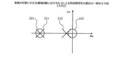
図2〜図5は、実施の形態にかかる増幅回路におけるA・βによる周波数特性の変化の一例を示す図である。図2〜図5のそれぞれは、横軸が実軸(Re)、縦軸が虚軸(Im)を示す複素平面である。また、図2〜図5は、それぞれA・β=1、A・β=0.9、A・β=0.8、A・β=0.7の場合における、HPF101および増幅回路110の組み合わせの周波数特性を、極211,212(×)および零点221,222(○)により示している。(Change in frequency characteristics due to A/β in the amplifier circuit according to the embodiment)
2 to 5 are diagrams showing an example of changes in frequency characteristics due to A.beta. in the amplifier circuit according to the embodiment. Each of FIGS. 2 to 5 is a complex plane in which the horizontal axis represents the real axis (Re) and the vertical axis represents the imaginary axis (Im). 2 to 5 show combinations of the
たとえば図2に示すように、A・β=1である場合は、極211,212および零点221,222がそれぞれ実軸上で重なり、互いに打ち消し合う。このため、HPF101および増幅回路110の組み合わせの周波数特性が平坦になる。また、図3〜図5に示すように、A・βが1より小さくなるほど、極212が実軸上で負の方向に移動し、零点222とのずれが大きくなる。このため、A・βが小さくなるほど、HPF101および増幅回路110の組み合わせの周波数特性が平坦でなくなる。 For example, as shown in FIG. 2, when A.beta.=1, the
(実施の形態にかかるHPFとLPFの遮断周波数)
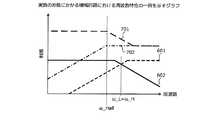
図6は、実施の形態にかかるHPFとLPFの遮断周波数の一例を示すグラフである。図6において、横軸は周波数を示し、縦軸は利得を示す。周波数特性601は、HPF101における周波数に対する利得の特性を示す。周波数特性602は、LPF113における周波数に対する利得の特性を示す。(Cutting frequency of HPF and LPF according to the embodiment)
FIG. 6 is a graph showing an example of cutoff frequencies of the HPF and the LPF according to the embodiment. In FIG. 6, the horizontal axis represents frequency and the vertical axis represents gain. The frequency characteristic 601 shows the characteristic of the gain with respect to the frequency in the
HPF101の低域の遮断角周波数ω_Hは、たとえば周波数特性601において利得が−3[dB]以下となる周波数範囲の上限の周波数である。LPF113の高域の遮断角周波数ω_Lは、周波数特性602において利得が−3[dB]以下となる周波数範囲の下限の周波数である。図6に示す例ではω_H=ω_Lとなっている。 The low-frequency cutoff angular frequency ω_H of the
(実施の形態にかかる増幅回路における周波数特性)
図7は、実施の形態にかかる増幅回路における周波数特性の一例を示すグラフである。図7において、図6に示した部分と同様の部分については同一の符号を付して説明を省略する。周波数特性701は、増幅回路110における周波数に対する利得の特性を示す。周波数特性702は、HPF101および増幅回路110を合わせた構成における周波数に対する利得の特性を示す。(Frequency characteristics in the amplifier circuit according to the embodiment)
FIG. 7 is a graph showing an example of frequency characteristics in the amplifier circuit according to the embodiment. 7, the same parts as those shown in FIG. 6 are designated by the same reference numerals, and the description thereof will be omitted. The frequency characteristic 701 shows the characteristic of the gain with respect to the frequency in the
増幅回路110の周波数特性701は、スロープ部分においてHPF101の周波数特性601と逆の特性となる。また、HPF101および増幅回路110を合わせた構成の周波数特性702における低域の遮断角周波数をω_Hallとすると、遮断角周波数ω_Hallは、HPF101の周波数特性601の低域の遮断角周波数ω_Hより低くなる。すなわち、増幅回路110を低周波数側に広帯域化することができる。 The
(実施の形態にかかる増幅回路を適用したTIA装置)
図8は、実施の形態にかかる増幅回路を適用したTIA装置の一例を示す図である。図8に示す光モジュール800は、フォトダイオード801と、コンデンサ802と、抵抗803と、TIA装置810と、を備える光モジュールである。実施の形態にかかる増幅回路110は、たとえば図8に示すTIA装置810に適用することができる。(TIA device to which the amplifier circuit according to the embodiment is applied)
FIG. 8 is a diagram showing an example of a TIA device to which the amplifier circuit according to the embodiment is applied. The
フォトダイオード801は、受光パワーに応じた電気信号を出力する受光素子である。TIA装置810は、フォトダイオード801から出力される電流信号を電圧信号に変換する。たとえば、TIA装置810は、フォトダイオード801のアノードに対して、コンデンサ802(C)を介して接続されている。コンデンサ802により、フォトダイオード801とTIA装置810との間はAC結合となっている。抵抗803(R)は、一端がフォトダイオード801のアノードとコンデンサ802との間に接続され、他端が接地されている。 The
TIA装置810は、ベース接地型TIA811と、エミッタフォロワ812と、出力端子813(out)と、LPF814と、帰還回路815と、バイアス部816(Vbias)と、を備える。 The
ベース接地型TIA811は、ベース接地型のTIA(Transimpedance Amplifier:インピーダンス変換増幅器)であって、図1に示した増幅器112に対応する構成である。たとえば、ベース接地型TIA811は、抵抗811a(R)と、バイポーラトランジスタ811bと、抵抗811c(R)と、電圧源811d(VCC)と、を備える。 The grounded-
抵抗811aは、一端がコンデンサ802とバイポーラトランジスタ811bとの間に接続され、他端が接地されている。バイポーラトランジスタ811bは、エミッタがコンデンサ802に接続され、ベースがバイアス部816に接続され、コレクタが抵抗811cおよびエミッタフォロワ812に接続されている。 The resistor 811a has one end connected between the
抵抗811cは、一端がバイポーラトランジスタ811bのコレクタおよびエミッタフォロワ812に接続され、他端が電圧源811dに接続されている。これにより、フォトダイオード801から出力された電流信号が電圧信号Vbに変換されてエミッタフォロワ812へ出力される。ベース接地型TIA811における利得が図1に示した増幅器112の利得Aに相当する。 The resistor 811c has one end connected to the collector and emitter follower 812 of the
エミッタフォロワ812は、バイポーラトランジスタ812aと、電圧源812b(VCC)と、抵抗812c(R)と、を備える。バイポーラトランジスタ812aは、ベースがベース接地型TIA811に接続され、コレクタが電圧源812bに接続され、エミッタがLPF814および出力端子813に接続されている。抵抗812cは、一端がバイポーラトランジスタ812aのエミッタとLPF814との間に接続され、他端が接地されている。 The emitter follower 812 includes a
出力端子813は、エミッタフォロワ812におけるバイポーラトランジスタ812aのエミッタとLPF814との間に接続されている。これにより、フォトダイオード801によって検出された光パワーを示す信号(電圧信号)を出力端子813から出力することができる。 The
LPF814は、図1に示したLPF113に対応する構成である。また、LPF814は、エミッタフォロワ812から出力された信号(電圧信号)のうちの所定の低周波成分のみを抽出し、抽出した低周波成分の信号を帰還回路815へ出力する。 The
帰還回路815は、利得部815a(G)と、帰還抵抗815b(Rf)と、を備える。利得部815aは、LPF814から出力された信号に所定の利得を与え、利得を与えた信号を帰還抵抗815bへ出力する。帰還抵抗815bは、利得部815aから出力された信号を電圧信号から電流信号に変換する。そして、帰還抵抗815bは、電流信号に変換した信号を、ベース接地型TIA811におけるバイポーラトランジスタ811bのエミッタへ入力することにより正帰還させる。帰還回路815における帰還率(利得)が図1に示した帰還回路114の帰還率(利得)βに相当する。 The
バイアス部816は、一端がバイポーラトランジスタ811bのベースに接続され、他端が接地されている。 The
図8に示すTIA装置810は、ベース接地型TIA811における利得Aと、帰還回路815における帰還率βと、の積A・βが0<A・β<1となるように設計される。これにより、正帰還における発振を抑制することができる。 The
また、LPF814の高域の遮断周波数は、コンデンサ802により形成されるハイパスフィルタの低域の遮断周波数と同等の(たとえば同じ)周波数とする。これにより、コンデンサ802の容量値を大きくしなくても、コンデンサ802およびTIA装置810の組み合わせにおける低域の遮断周波数を低くすることができる。このため、たとえば出力端子813から出力される信号におけるサグを抑制することができる。 Further, the cutoff frequency in the high band of the
図8に示したように、図1に示した増幅器112は、たとえば、トランジスタのベースを接地するベース接地のトランジスタ増幅回路(たとえばベース接地型TIA811)に適用することができる。また、このトランジスタ増幅回路(たとえばベース接地型TIA811)には、トランジスタ増幅回路によって増幅された信号を出力するエミッタフォロワ812が接続されていてもよい。 As shown in FIG. 8, the
また、図1に示した帰還回路114は、増幅器112から出力された信号を増幅する増幅部(たとえば利得部815a)と、増幅器112から出力された信号を通過させる抵抗(帰還抵抗815b)と、を含む構成とすることができる。 Further, the
(実施の形態にかかる増幅回路を適用した差動トランスインピーダンスアンプ)
図9は、実施の形態にかかる増幅回路を適用した差動トランスインピーダンスアンプの一例を示す図である。図9において、図8に示した部分と同様の部分については同一の符号を付して説明を省略する。図9に示す光モジュール900は、フォトダイオード801と、コンデンサ901a,901bと、抵抗902a,902b(R)と、差動トランスインピーダンスアンプ910と、を備える光モジュールである。(Differential transimpedance amplifier to which the amplifier circuit according to the embodiment is applied)
FIG. 9 is a diagram showing an example of a differential transimpedance amplifier to which the amplifier circuit according to the embodiment is applied. 9, the same parts as those shown in FIG. 8 are designated by the same reference numerals and the description thereof will be omitted. The
実施の形態にかかる増幅回路110は、たとえば図9に示す差動トランスインピーダンスアンプ910に適用することができる。図9に示す例では、差動トランスインピーダンスアンプ910は、フォトダイオード801から出力される差動の電流信号を電圧信号に変換する。たとえば、差動トランスインピーダンスアンプ910は、フォトダイオード801のカソードに対してコンデンサ901aを介して接続され、フォトダイオード801のアノードに対してコンデンサ901bを介して接続される。 The
抵抗902aは、一端がフォトダイオード801のカソードとコンデンサ901aとの間に接続され、他端が接地されている。抵抗902bは、一端がフォトダイオード801のアノードとコンデンサ901bとの間に接続され、他端が接地されている。コンデンサ901a,901bにより、フォトダイオード801と差動トランスインピーダンスアンプ910との間はAC結合となっている。 The
差動トランスインピーダンスアンプ910は、差動増幅器911と、出力端子912a,912bと、抵抗913a,913bと、LPF914a,914bと、利得部915a,915bと、抵抗916a,916bと、を備える。 The
差動増幅器911は、正の入力端子(+)および負の入力端子(−)を有し、図1に示した増幅器112に対応する構成である。差動増幅器911の正の入力端子(+)は、コンデンサ901aを介してフォトダイオード801のカソードと接続されている。差動増幅器911の負の入力端子(−)は、コンデンサ901bを介してフォトダイオード801のアノードと接続されている。 The
差動増幅器911は、正の入力端子(+)および負の入力端子(−)から入力された各信号を差動増幅し、差動増幅により得られた正転信号および反転信号を出力する。差動増幅器911からの正転信号は、出力端子912aから出力(Outp)されるとともに、抵抗913aおよびLPF914aへ入力される。差動増幅器911からの反転信号は、出力端子912bから出力(Outn)されるとともに、抵抗913bおよびLPF914bへ入力される。差動増幅器911における利得が図1に示した増幅器112の利得Aに相当する。 The
抵抗913aは、差動増幅器911からの正転信号を電圧信号から電流信号に変換し、変換した正転信号を差動増幅器911の正の入力端子(+)へフィードバックする。抵抗913bは、差動増幅器911からの反転信号を電圧信号から電流信号に変換し、変換した反転信号を差動増幅器911の負の入力端子(−)へフィードバックする。 The
LPF914a,914bは、図1に示したLPF113に対応する構成である。LPF914aは、差動増幅器911からの正転信号のうちの所定の低周波成分のみを抽出し、抽出した低周波成分の正転信号を利得部915aへ出力する。LPF914bは、差動増幅器911からの反転信号のうちの所定の低周波成分のみを抽出し、抽出した低周波成分の反転信号を利得部915bへ出力する。 The
利得部915a,915bおよび抵抗916a,916bは、図1に示した帰還回路114に対応する構成である。利得部915a,915bおよび抵抗916a,916bにおける帰還率(利得)が図1に示した帰還回路114の帰還率(利得)βに相当する。 The
利得部915aは、LPF914aから出力された正転信号に所定の利得を与え、利得を与えた正転信号を、抵抗916aへ出力する。抵抗916aは、LPF914aから出力された正転信号を電圧信号から電流信号に変換し、変換した正転信号を差動増幅器911の負の入力端子(−)へフィードバックする。 The
利得部915bは、LPF914bから出力された反転信号に所定の利得を与え、利得を与えた反転信号を、抵抗916bへ出力する。抵抗916bは、LPF914bから出力された反転信号を電圧信号から電流信号に変換し、変換した反転信号を差動増幅器911の正の入力端子(+)へフィードバックする。 The
図9に示す差動トランスインピーダンスアンプ910は、差動増幅器911における利得Aと、利得部915a,915bおよび抵抗916a,916bにおける帰還率βと、の積A・βが0<A・β<1となるように設計される。これにより、正帰還における発振を抑制することができる。 In the
また、LPF914a,914bの高域の遮断周波数は、コンデンサ901a,901bにより形成されるハイパスフィルタの低域の遮断周波数と同等の(たとえば同じ)周波数とする。これにより、コンデンサ901a,901bの容量値を大きくしなくても、コンデンサ901a,901bおよび差動トランスインピーダンスアンプ910の組み合わせにおける低域の遮断周波数を低くすることができる。このため、たとえば出力端子912a,912bから出力される信号におけるサグを抑制することができる。 Further, the high-frequency cutoff frequency of the
図9に示したように、増幅回路110は、たとえば差動増幅器911に適用することができる。この場合に、帰還回路114は、差動増幅器911の正転出力を差動増幅器911の入力に正帰還させる第1帰還回路と、差動増幅器911の反転出力を差動増幅器911の入力に正帰還させる第2帰還回路と、を含む構成とすることができる。この場合の第1帰還回路は、たとえば図9に示した利得部915aおよび抵抗916aである。また、第2帰還回路は、たとえば図9に示した利得部915bおよび抵抗916bである。 As shown in FIG. 9, the
(実施の形態にかかる増幅回路を適用した光インターコネクトシステム)
図10は、実施の形態にかかる増幅回路を適用した光インターコネクトシステムの一例を示す図である。実施の形態にかかる増幅回路110は、たとえば図10に示す光インターコネクトシステム1000に適用することができる。光インターコネクトシステム1000は、第1装置1010と第2装置1050との間のデータ伝送に光通信を行う光インターコネクトのシステムである。第1装置1010および第2装置1050のそれぞれは、たとえばCPU(Central Processing Unit:中央処理装置)などのプロセッサである。(Optical interconnect system to which the amplifier circuit according to the embodiment is applied)
FIG. 10 is a diagram showing an example of an optical interconnect system to which the amplifier circuit according to the embodiment is applied. The
図10に示すように、光インターコネクトシステム1000は、第1装置1010と、送信器1020と、光伝送路1030と、受信器1040と、第2装置1050と、を含む。第1装置1010は、第2装置1050へ伝送するデータを示す電気信号を生成し、生成した電気信号を送信器1020へ出力する。 As shown in FIG. 10, the
送信器1020は、発光素子駆動回路1021と、発光素子1022と、を備える光モジュールである。発光素子駆動回路1021は、第1装置1010から出力された電気信号を増幅することにより、発光素子1022を駆動する電気信号(駆動信号)を生成する。そして、発光素子駆動回路1021は、生成した電気信号を発光素子1022へ出力する。発光素子1022は、発光素子駆動回路1021から出力された電気信号に応じた光を発振し、発振した光を光信号として光伝送路1030へ出射する。発光素子1022には、たとえばLD(Laser Diode)を用いることができる。 The
光伝送路1030は、送信器1020から出射された光信号を伝播させて受信器1040へ出射する。光伝送路1030には、たとえば光ファイバなどの導波路を用いることができる。また、光伝送路1030は、光を伝播させる空間であってもよい。 The
受信器1040は、光電変換回路1041と、低雑音増幅回路1042と、イコライザ/リミットアンプ1043と、識別回路1044と、を備える光モジュールである。光電変換回路1041は、光伝送路1030から出射された光信号を電気信号に変換し、変換した電気信号を低雑音増幅回路1042へ出力する受光素子である。光電変換回路1041には、たとえばPD(Photo Diode)を用いることができる。 The
低雑音増幅回路1042は、光電変換回路1041から出力された電気信号を低雑音で増幅し、増幅した電気信号をイコライザ/リミットアンプ1043へ出力する。また、光電変換回路1041と低雑音増幅回路1042との接続は、コンデンサを介した接続、すなわちAC結合になっている。 The low-noise amplifier circuit 1042 amplifies the electric signal output from the photoelectric conversion circuit 1041 with low noise, and outputs the amplified electric signal to the equalizer/
実施の形態にかかる増幅回路110は、たとえば低雑音増幅回路1042に適用することができる。これにより、光電変換回路1041と低雑音増幅回路1042との間のAC結合のコンデンサ容量を大きくしなくても、低域の遮断周波数を低くすることができる。このため、たとえば低雑音増幅回路1042からイコライザ/リミットアンプ1043へ出力される信号におけるサグを抑制することができる。 The
イコライザ/リミットアンプ1043は、低雑音増幅回路1042から出力された電気信号の等化処理や増幅を行い、等化処理や増幅を行った電気信号を識別回路1044へ出力する。識別回路1044は、イコライザ/リミットアンプ1043から出力された電気信号の識別再生を行い、識別再生により得られた信号(データ)を第2装置1050へ出力する。第2装置1050は、受信器1040から出力された信号に基づく処理を行う。 The equalizer/
(実施の形態にかかる増幅回路における周波数特性のシミュレーション結果)
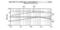
図11〜図13は、実施の形態にかかる増幅回路における周波数特性のシミュレーション結果の一例を示すグラフである。図11〜図13において、図7に示した部分と同様の部分については同一の符号を付して説明を省略する。図11〜図13においては、それぞれA・β=0.7、A・β=0.8、A・β=0.9とした場合における周波数特性601,602,701,702を示している。(Result of Simulation of Frequency Characteristics in Amplifier Circuit According to Embodiment)
11 to 13 are graphs showing examples of simulation results of frequency characteristics in the amplifier circuit according to the embodiment. 11 to 13, the same parts as those shown in FIG. 7 are designated by the same reference numerals, and the description thereof will be omitted. 11 to 13
上述のように、周波数特性601,602は、それぞれHPF101およびLPF113の周波数特性である。周波数特性701は、増幅回路110の周波数特性を示す。周波数特性702は、HPF101および増幅回路110の組み合わせの周波数特性を示す。 As described above, the
また、図11〜図13に示す例では、HPF101の周波数特性601の低域の遮断角周波数ω_Hと、LPF113の周波数特性602の高域の遮断角周波数ω_Lと、をともに628[Mrad/s]としている。 Further, in the examples shown in FIGS. 11 to 13, both the cutoff angular frequency ω_H in the low frequency range of the
図11の周波数特性702に示すように、A・β=0.7とした場合におけるHPF101および増幅回路110の組み合わせの低域の遮断角周波数ω_Hallは188[Mrad/s]となっている。図12の周波数特性702に示すように、A・β=0.8とした場合におけるHPF101および増幅回路110の組み合わせの低域の遮断角周波数ω_Hallは126[Mrad/s]となっている。図13の周波数特性702に示すように、A・β=0.9とした場合におけるHPF101および増幅回路110の組み合わせの低域の遮断角周波数ω_Hallは62.8[Mrad/s]となっている。 As shown by the frequency characteristic 702 in FIG. 11, the low cutoff angular frequency ω_Hall of the combination of the
図11〜図13に示すように、増幅回路110によれば、HPF101および増幅回路110の組み合わせの低域の遮断角周波数ω_Hallを、HPF101だけの低域の遮断角周波数ω_H(628[Mrad/s])より低くすることができる。たとえば、A・β=0.9とすることで、HPF101および増幅回路110の組み合わせの低域の遮断角周波数ω_Hallを、HPF101だけの低域の遮断角周波数ω_H(628[Mrad/s])の1/10の62.8[Mrad/s]にできる。 As shown in FIGS. 11 to 13, according to the
これにより、HPF101(AC結合部)のコンデンサの容量値を大きくしなくても、HPF101および増幅回路110の組み合わせの低域の遮断角周波数ω_Hallを低くすることができる。 As a result, the low cutoff angular frequency ω_Hall of the combination of the
(増幅回路の出力信号におけるサグ)
図14は、増幅回路の出力信号におけるサグの一例を示す参考図である。図14において、横軸は時間を示し、縦軸は電圧(V)を示す。出力波形1400は、たとえばAC結合によって低域の遮断角周波数が高くなっている増幅回路から出力される信号の波形である。低域の遮断角周波数が高い増幅回路に対して、同じ符号が長期間連続する信号を入力すると、同じ符号が長期間連続する信号が低周波成分として遮断されることによるサグが発生する(たとえばサグ1401)。このため、たとえば増幅回路の後段の回路によって電気信号の値(0または1)を識別する際に誤りが生じる場合がある。(Sag in the output signal of the amplifier circuit)
FIG. 14 is a reference diagram showing an example of sag in the output signal of the amplifier circuit. In FIG. 14, the horizontal axis represents time and the vertical axis represents voltage (V). The
これに対して、増幅回路110によれば、上述したように低域の遮断角周波数ω_Hallを低くすることができるため、サグを抑制することができる。このため、増幅回路110の後段の回路によって電気信号の値(0または1)を識別する際の誤りを抑制することができる。 On the other hand, according to the
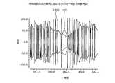
(増幅回路の出力信号のアイパターン)
図15は、増幅回路の出力信号のアイパターンの一例を示す参考図である。図15において、横軸は時間を示し、縦軸は電圧(V)を示す。アイパターン1500は、低域の遮断角周波数が高い増幅回路から出力される信号のアイパターンである。アイパターン1500に示すように、低域の遮断角周波数が高い増幅回路から出力される信号は、サグによってアイ開口が狭くなる。(Eye pattern of output signal of amplifier circuit)
FIG. 15 is a reference diagram showing an example of the eye pattern of the output signal of the amplifier circuit. In FIG. 15, the horizontal axis represents time and the vertical axis represents voltage (V). The
(実施の形態にかかる増幅回路の出力信号のアイパターン)
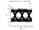
図16は、実施の形態にかかる増幅回路の出力信号のアイパターンの一例を示す図である。図16において、横軸は時間を示し、縦軸は電圧(V)を示す。アイパターン1600は、実施の形態にかかる増幅回路110から出力される信号のアイパターンである。アイパターン1600に示すように、増幅回路110から出力される信号は、サグが抑制されるため、アイ開口が広くなる。このように、増幅回路110によれば、出力信号の品質を向上させることができる。(Eye pattern of the output signal of the amplifier circuit according to the embodiment)
FIG. 16 is a diagram showing an example of the eye pattern of the output signal of the amplifier circuit according to the embodiment. In FIG. 16, the horizontal axis represents time and the vertical axis represents voltage (V). The
(実施の形態にかかる増幅回路の他の例)
図17は、実施の形態にかかる増幅回路の他の例を示す図である。図17において、図1に示した部分と同様の部分については同一の符号を付して説明を省略する。図17に示すように、実施の形態にかかる増幅回路110は、増幅回路110の後段の回路との間でAC結合された構成であってもよい。たとえば、増幅回路110の後段の回路と増幅回路110との間には直列にコンデンサが設けられている。このため、図17に示すように、増幅回路110の出力にはAC結合によるHPF101が形成される。(Another Example of Amplifier Circuit According to Embodiment)
FIG. 17 is a diagram illustrating another example of the amplifier circuit according to the embodiment. 17, the same parts as those shown in FIG. 1 are designated by the same reference numerals and the description thereof will be omitted. As shown in FIG. 17, the
たとえば上記(4)式に示したように、HPF101および増幅回路110の組み合わせの周波数特性は、HPF101の周波数特性601と、増幅回路110の周波数特性701と、を乗算した特性となる。したがって、図17に示すHPF101および増幅回路110の組み合わせの周波数特性は、図1に示したHPF101および増幅回路110の組み合わせの周波数特性と同じになる。このため、図17に示す構成においても、図1に示した構成と同様に、AC結合のコンデンサ容量を大きくしなくても低域の遮断周波数を低くすることができる。 For example, as shown in the equation (4), the frequency characteristic of the combination of the
図17に示した増幅回路110は、たとえば図10に示した発光素子駆動回路1021と発光素子1022がAC結合により接続されている場合に、発光素子駆動回路1021に適用することができる。これにより、発光素子1022へ出力される電気信号におけるサグを抑制することができる。 The
このように、実施の形態にかかる増幅回路110は、帰還回路114および合成部111によって増幅器112の入力へ正帰還する信号の高周波成分を減衰させるLPF113を設けた構成である。これにより、AC結合により形成されるHPF101および増幅回路110の組み合わせにおける低域の遮断周波数を、HPF101における低域の遮断周波数より低くすることができる。 As described above, the
このため、AC結合のコンデンサ容量を大きくしなくても低域の遮断周波数を低くすることができる。したがって、装置の大型化を抑制しつつ、AC結合によって信号の低周波成分が減衰することによるサグの発生を抑制することができる。 Therefore, it is possible to lower the cutoff frequency in the low frequency range without increasing the capacity of the AC coupling capacitor. Therefore, it is possible to suppress the occurrence of sag due to the attenuation of the low frequency component of the signal due to the AC coupling while suppressing the increase in size of the device.
また、帰還回路114および合成部111による正帰還のループ利得を1より小さくすることで、帰還回路114および合成部111の正帰還による発振を抑制することができる。これにより、増幅回路110の動作を安定させることができる。 Further, by making the loop gain of the positive feedback by the
また、上述した実施の形態においては、LPF113の高域の遮断周波数がHPF101の低域の遮断周波数とほぼ同じである構成について説明したが、LPF113の高域の遮断周波数はHPF101の低域の遮断周波数と同じ周波数に限らない。 Further, in the above-described embodiment, the high-frequency cutoff frequency of the
すなわち、LPF113の高域の遮断周波数は、HPF101および増幅回路110の組み合わせにおける低域の遮断周波数が、HPF101における低域の遮断周波数より低くなる範囲で設定すればよい。これにより、AC結合の構成において低域の遮断周波数を低くすることができる。 That is, the high cutoff frequency of the
また、LPF113を帰還回路114の前段に設ける構成について説明したが、LPF113を帰還回路114の後段に設ける構成、すなわちLPF113を帰還回路114と合成部111との間に設ける構成としてもよい。 Further, although the configuration in which the
以上説明したように、増幅回路、光モジュールおよび増幅方法によれば、AC結合のコンデンサ容量を大きくしなくても低域の遮断周波数を低くすることができる。 As described above, according to the amplifying circuit, the optical module, and the amplifying method, the cutoff frequency in the low frequency band can be lowered without increasing the capacitance of the AC coupling capacitor.
たとえば、AC結合により接続された増幅回路において、増幅回路の入出力間に、AC結合による低域遮断周波数と同等の遮断周波数を備えるLPFと、帰還回路と、が直列接続され、ループ利得<1の条件で正帰還をかける構成とする。これにより、AC結合のコンデンサ容量を大きくしなくても、低域の遮断周波数を低くすることができる。 For example, in an amplifier circuit connected by AC coupling, an LPF having a cutoff frequency equivalent to the low cutoff frequency by AC coupling and a feedback circuit are connected in series between the input and output of the amplifier circuit, and a loop gain <1. The positive feedback is applied under the condition of. As a result, the cutoff frequency in the low frequency range can be lowered without increasing the capacity of the AC coupling capacitor.
上述した各実施の形態に関し、さらに以下の付記を開示する。 The following supplementary notes will be disclosed regarding the above-described embodiments.
(付記1)AC(Alternating Current:交流)結合により他回路と接続された増幅回路であって、
前記他回路から入力された信号を増幅して出力する、または入力された信号を増幅して前記他回路へ出力する増幅器と、
前記増幅器から出力された信号を前記増幅器の入力に正帰還させる帰還回路と、
前記帰還回路によって前記増幅器の入力へ正帰還する信号の高周波成分を減衰させるローパスフィルタであって、自増幅回路と前記AC結合により形成されるハイパスフィルタとの組み合わせにおける低域の遮断周波数が、前記ハイパスフィルタにおける低域の遮断周波数より低くなるように高域の遮断周波数が設定されたローパスフィルタと、
を備えることを特徴とする増幅回路。(Supplementary Note 1) An amplifier circuit connected to another circuit by AC (Alternating Current) coupling,
An amplifier for amplifying and outputting a signal input from the other circuit, or for amplifying an input signal and outputting the amplified signal to the other circuit,
A feedback circuit for positively feeding back the signal output from the amplifier to the input of the amplifier;
A low pass filter for attenuating a high frequency component of a signal positively fed back to the input of the amplifier by the feedback circuit, wherein a low cutoff frequency in a combination of a self amplifying circuit and a high pass filter formed by the AC coupling is A low-pass filter in which the high-frequency cutoff frequency is set to be lower than the low-frequency cutoff frequency in the high-pass filter,
An amplification circuit comprising:
(付記2)前記ローパスフィルタの高域の遮断周波数は、前記ハイパスフィルタにおける低域の遮断周波数と同等であることを特徴とする付記1に記載の増幅回路。(Supplementary Note 2) The amplifier circuit according to
(付記3)前記帰還回路は、前記増幅器から出力された信号を、前記信号のループ利得が1より小さくなるように前記増幅器の入力に正帰還させることを特徴とする付記1または2に記載の増幅回路。(Additional remark 3) The feedback circuit positively feeds back the signal output from the amplifier to the input of the amplifier so that the loop gain of the signal becomes smaller than 1. Amplifier circuit.
(付記4)前記増幅器は、前記信号を増幅するベース接地のトランジスタ増幅回路を含むことを特徴とする付記1〜3のいずれか一つに記載の増幅回路。(Supplementary Note 4) The amplifier circuit according to any one of
(付記5)前記増幅器は、前記トランジスタ増幅回路によって増幅された前記信号を出力するエミッタフォロワを含むことを特徴とする付記4に記載の増幅回路。(Supplementary note 5) The amplifier circuit according to
(付記6)前記帰還回路は、前記増幅器から出力された信号を増幅する増幅部と、前記増幅器から出力された信号を通過させる抵抗と、を含むことを特徴とする付記1〜5のいずれか一つに記載の増幅回路。(Supplementary Note 6) The feedback circuit includes an amplification unit that amplifies a signal output from the amplifier, and a resistor that allows a signal output from the amplifier to pass therethrough. The amplifier circuit according to one.
(付記7)前記増幅器は差動増幅器であり、
前記帰還回路は、前記差動増幅器の正転出力を前記差動増幅器の入力に正帰還させる第1帰還回路と、前記差動増幅器の反転出力を前記差動増幅器の入力に正帰還させる第2帰還回路と、を含む、
ことを特徴とする付記1〜6のいずれか一つに記載の増幅回路。(Supplementary Note 7) The amplifier is a differential amplifier,
The feedback circuit includes a first feedback circuit that positively feeds back a normal output of the differential amplifier to an input of the differential amplifier, and a second feedback circuit that feeds back an inverted output of the differential amplifier to an input of the differential amplifier. Including a feedback circuit,
The amplifier circuit according to any one of
(付記8)受光パワーに応じた電気信号を出力する受光素子と、
AC(Alternating Current:交流)結合により前記受光素子と接続され、前記受光素子からの信号を増幅して出力する増幅器と、
前記増幅器から出力された信号を、前記信号のループ利得が1より小さくなるように前記増幅器の入力に正帰還させる帰還回路と、
前記帰還回路によって前記増幅器の入力へ正帰還する信号の高周波成分を減衰させるローパスフィルタであって、自増幅回路と前記AC結合により形成されるハイパスフィルタとの組み合わせにおける低域の遮断周波数が、前記ハイパスフィルタにおける低域の遮断周波数より低くなるように高域の遮断周波数が設定されたローパスフィルタと、
を備えることを特徴とする光モジュール。(Supplementary Note 8) A light receiving element that outputs an electric signal according to received light power,
An amplifier that is connected to the light receiving element by AC (Alternating Current) coupling and that amplifies and outputs a signal from the light receiving element,
A feedback circuit for positively feeding back the signal output from the amplifier to the input of the amplifier so that the loop gain of the signal becomes less than 1.
A low pass filter for attenuating a high frequency component of a signal positively fed back to the input of the amplifier by the feedback circuit, wherein a low cutoff frequency in a combination of a self amplifying circuit and a high pass filter formed by the AC coupling is A low-pass filter in which the high-frequency cutoff frequency is set to be lower than the low-frequency cutoff frequency in the high-pass filter,
An optical module comprising:
(付記9)入力された電気信号に応じた光を出射する発光素子と、
AC(Alternating Current:交流)結合により前記発光素子と接続され、入力された信号を増幅して前記発光素子へ出力する増幅器と、
前記増幅器から出力された信号を、前記信号のループ利得が1より小さくなるように前記増幅器の入力に正帰還させる帰還回路と、
前記帰還回路によって前記増幅器の入力へ正帰還する信号の高周波成分を減衰させるローパスフィルタであって、自増幅回路と前記AC結合により形成されるハイパスフィルタとの組み合わせにおける低域の遮断周波数が、前記ハイパスフィルタにおける低域の遮断周波数より低くなるように高域の遮断周波数が設定されたローパスフィルタと、
を備えることを特徴とする光モジュール。(Supplementary Note 9) A light emitting element that emits light according to an input electric signal,
An amplifier that is connected to the light emitting element by AC (Alternating Current) coupling and amplifies an input signal and outputs the amplified signal to the light emitting element.
A feedback circuit for positively feeding back the signal output from the amplifier to the input of the amplifier so that the loop gain of the signal becomes less than 1.
A low pass filter for attenuating a high frequency component of a signal positively fed back to the input of the amplifier by the feedback circuit, wherein a low cutoff frequency in a combination of a self amplifying circuit and a high pass filter formed by the AC coupling is A low-pass filter in which the high-frequency cutoff frequency is set to be lower than the low-frequency cutoff frequency in the high-pass filter,
An optical module comprising:
(付記10)AC(Alternating Current:交流)結合により他回路と接続された増幅回路であって、前記他回路から入力された信号を増幅して出力する、または入力された信号を増幅して前記他回路へ出力する増幅器を備える増幅回路による増幅方法において、
前記増幅器から出力された信号を、前記信号のループ利得が1より小さくなるように前記増幅器の入力に正帰還させ、
自増幅回路と前記AC結合により形成されるハイパスフィルタとの組み合わせにおける低域の遮断周波数が、前記ハイパスフィルタにおける低域の遮断周波数より低くなるように高域の遮断周波数が設定されたローパスフィルタにより、前記増幅器の入力へ正帰還する前記信号の高周波成分を減衰させる、
ことを特徴とする増幅方法。(Supplementary note 10) An amplifier circuit connected to another circuit by AC (Alternating Current) coupling, which amplifies and outputs a signal input from the other circuit, or amplifies an input signal and outputs the signal. In an amplification method using an amplification circuit including an amplifier that outputs to another circuit,
The signal output from the amplifier is positively fed back to the input of the amplifier so that the loop gain of the signal is less than 1.
A low-pass filter in which a high-frequency cutoff frequency is set so that a low-frequency cutoff frequency in a combination of a self-amplification circuit and a highpass filter formed by the AC coupling is lower than a low-frequency cutoff frequency in the highpass filter. Attenuating high frequency components of the signal that are positively fed back to the input of the amplifier,
An amplification method characterized by the above.
101 HPF
110 増幅回路
111 合成部
112 増幅器
113,814,914a,914b LPF
114,815 帰還回路
211,212 極
221,222 零点
601,602,701,702 周波数特性
800,900 光モジュール
801 フォトダイオード
802,901a,901b コンデンサ
803,811a,811c,812c,902a,902b,913a,913b,916a,916b 抵抗
810 TIA装置
811 ベース接地型TIA
811b,812a バイポーラトランジスタ
811d,812b 電圧源
812 エミッタフォロワ
813,912a,912b 出力端子
815a,915a,915b 利得部
815b 帰還抵抗
816 バイアス部
910 差動トランスインピーダンスアンプ
911 差動増幅器
1000 光インターコネクトシステム
1010 第1装置
1020 送信器
1021 発光素子駆動回路
1022 発光素子
1030 光伝送路
1040 受信器
1041 光電変換回路
1042 低雑音増幅回路
1043 イコライザ/リミットアンプ
1044 識別回路
1050 第2装置
1400 出力波形
1401 サグ
1500,1600 アイパターン101 HPF
110
114,815 Feedback circuit 211,212 Pole 221,222 Zero point 601,602,701,702 Frequency characteristic 800,900
811b, 812a
Claims (6)
Translated fromJapanese前記他回路から入力された信号を増幅して出力する、または入力された信号を増幅して前記他回路へ出力する増幅器と、
前記増幅器から出力された信号を前記増幅器の入力に正帰還させる帰還回路と、
前記帰還回路によって前記増幅器の入力へ正帰還する信号の高周波成分を減衰させるローパスフィルタであって、自増幅回路と前記AC結合により形成されるハイパスフィルタとの組み合わせにおける低域の遮断周波数が、前記ハイパスフィルタにおける低域の遮断周波数より低くなるように高域の遮断周波数が設定されたローパスフィルタと、を備え、
前記ローパスフィルタの高域の遮断周波数は、前記ローパスフィルタからの出力信号が前記ローパスフィルタへの入力信号に対して3dB以上減衰する周波数範囲の下限に設定され、前記ハイパスフィルタの低域の遮断周波数は、前記ハイパスフィルタからの出力信号が前記ハイパスフィルタへの入力信号に対して3dB以上減衰する周波数範囲の上限に設定され、
前記帰還回路は、前記増幅器から出力された信号を、前記信号のループ利得が1より小さくなるように前記増幅器の入力に正帰還させ、前記増幅器の利得Aと、前記帰還回路の帰還率βとの積A・βが0<A・β<1であることを特徴とする増幅回路。An amplifier circuit connected to another circuit by AC (Alternating Current) coupling,
An amplifier for amplifying and outputting a signal input from the other circuit, or for amplifying an input signal and outputting the amplified signal to the other circuit,
A feedback circuit for positively feeding back the signal output from the amplifier to the input of the amplifier;
A low pass filter for attenuating a high frequency component of a signal positively fed back to the input of the amplifier by the feedback circuit, wherein a low cutoff frequency in a combination of a self amplifying circuit and a high pass filter formed by the AC coupling is A low pass filter having a high cutoff frequency set to be lower than the low cutoff frequency in the high pass filter,
The high cutoff frequency of the low pass filter is set to the lower limit of the frequency range in which the output signal from the low pass filter is attenuated by 3 dB or more with respect to the input signal to the low pass filter, and the low cutoff frequency of the high pass filter is set. Is set to the upper limit of the frequency range in which the output signal from the high-pass filter is attenuated by 3 dB or more with respect to the input signal to the high-pass filter,
The feedback circuit positively feeds back the signal output from the amplifier to the input of the amplifier so that the loop gain of the signal becomes less than 1, and the gain A of the amplifier and the feedback ratio β of the feedback circuit are set. An amplifier circuit characterized in thatthe product A·β of 0<A·β<1 .
AC(Alternating Current:交流)結合により前記受光素子と接続され、前記受光素子からの信号を増幅して出力する増幅器と、
前記増幅器から出力された信号を前記増幅器の入力に正帰還させる帰還回路と、
前記帰還回路によって前記増幅器の入力へ正帰還する信号の高周波成分を減衰させるローパスフィルタであって、自増幅回路と前記AC結合により形成されるハイパスフィルタとの組み合わせにおける低域の遮断周波数が、前記ハイパスフィルタにおける低域の遮断周波数より低くなるように高域の遮断周波数が設定されたローパスフィルタと、を備え、
前記ローパスフィルタの高域の遮断周波数は、前記ローパスフィルタからの出力信号が前記ローパスフィルタへの入力信号に対して3dB以上減衰する周波数範囲の下限に設定され、前記ハイパスフィルタの低域の遮断周波数は、前記ハイパスフィルタからの出力信号が前記ハイパスフィルタへの入力信号に対して3dB以上減衰する周波数範囲の上限に設定され、
前記帰還回路は、前記増幅器から出力された信号を、前記信号のループ利得が1より小さくなるように前記増幅器の入力に正帰還させ、前記増幅器の利得Aと、前記帰還回路の帰還率βとの積A・βが0<A・β<1であることを特徴とする光モジュール。A light receiving element that outputs an electric signal according to the light receiving power,
An amplifier that is connected to the light receiving element by AC (Alternating Current) coupling and that amplifies and outputs a signal from the light receiving element,
A feedback circuit for positively feeding back the signal output from the amplifier to the input of the amplifier;
A low pass filter for attenuating a high frequency component of a signal positively fed back to the input of the amplifier by the feedback circuit, wherein a low cutoff frequency in a combination of a self amplifying circuit and a high pass filter formed by the AC coupling is A low pass filter having a high cutoff frequency set to be lower than the low cutoff frequency in the high pass filter,
The high cutoff frequency of the low pass filter is set to the lower limit of the frequency range in which the output signal from the low pass filter is attenuated by 3 dB or more with respect to the input signal to the low pass filter, and the low cutoff frequency of the high pass filter is set. Is set to the upper limit of the frequency range in which the output signal from the high-pass filter is attenuated by 3 dB or more with respect to the input signal to the high-pass filter,
The feedback circuit positively feeds back the signal output from the amplifier to the input of the amplifier so that the loop gain of the signal becomes less than 1, and the gain A of the amplifier and the feedback ratio β of the feedback circuit are set. An optical module characterized in thatthe product A·β of 0<A·β<1 .
AC(Alternating Current:交流)結合により前記発光素子と接続され、入力された信号を増幅して前記発光素子へ出力する増幅器と、
前記増幅器から出力された信号を前記増幅器の入力に正帰還させる帰還回路と、
前記帰還回路によって前記増幅器の入力へ正帰還する信号の高周波成分を減衰させるローパスフィルタであって、自増幅回路と前記AC結合により形成されるハイパスフィルタとの組み合わせにおける低域の遮断周波数が、前記ハイパスフィルタにおける低域の遮断周波数より低くなるように高域の遮断周波数が設定されたローパスフィルタと、を備え、
前記ローパスフィルタの高域の遮断周波数は、前記ローパスフィルタからの出力信号が前記ローパスフィルタへの入力信号に対して3dB以上減衰する周波数範囲の下限に設定され、前記ハイパスフィルタの低域の遮断周波数は、前記ハイパスフィルタからの出力信号が前記ハイパスフィルタへの入力信号に対して3dB以上減衰する周波数範囲の上限に設定され、
前記帰還回路は、前記増幅器から出力された信号を、前記信号のループ利得が1より小さくなるように前記増幅器の入力に正帰還させ、前記増幅器の利得Aと、前記帰還回路の帰還率βとの積A・βが0<A・β<1であることを特徴とする光モジュール。A light emitting element that emits light according to an input electric signal,
An amplifier that is connected to the light emitting element by AC (Alternating Current) coupling and amplifies an input signal and outputs the amplified signal to the light emitting element.
A feedback circuit for positively feeding back the signal output from the amplifier to the input of the amplifier;
A low pass filter for attenuating a high frequency component of a signal positively fed back to the input of the amplifier by the feedback circuit, wherein a low cutoff frequency in a combination of a self amplifying circuit and a high pass filter formed by the AC coupling is A low pass filter having a high cutoff frequency set to be lower than the low cutoff frequency in the high pass filter,
The high cutoff frequency of the low pass filter is set to the lower limit of the frequency range in which the output signal from the low pass filter is attenuated by 3 dB or more with respect to the input signal to the low pass filter, and the low cutoff frequency of the high pass filter is set. Is set to the upper limit of the frequency range in which the output signal from the high-pass filter is attenuated by 3 dB or more with respect to the input signal to the high-pass filter,
The feedback circuit positively feeds back the signal output from the amplifier to the input of the amplifier so that the loop gain of the signal becomes less than 1, and the gain A of the amplifier and the feedback ratio β of the feedback circuit are set. An optical module characterized in thatthe product A·β of 0<A·β<1 .
前記増幅器から出力された信号を前記増幅器の入力に正帰還させ、
自増幅回路と前記AC結合により形成されるハイパスフィルタとの組み合わせにおける低域の遮断周波数が、前記ハイパスフィルタにおける低域の遮断周波数より低くなるように高域の遮断周波数が設定されたローパスフィルタにより、前記増幅器の入力へ正帰還する前記信号の高周波成分を減衰させ、
前記ローパスフィルタの高域の遮断周波数は、前記ローパスフィルタからの出力信号が前記ローパスフィルタへの入力信号に対して3dB以上減衰する周波数範囲の下限に設定し、前記ハイパスフィルタの低域の遮断周波数は、前記ハイパスフィルタからの出力信号が前記ハイパスフィルタへの入力信号に対して3dB以上減衰する周波数範囲の上限に設定し、
前記帰還回路は、前記増幅器から出力された信号を、前記信号のループ利得が1より小さくなるように前記増幅器の入力に正帰還させ、前記増幅器の利得Aと、前記帰還回路の帰還率βとの積A・βが0<A・β<1であることを特徴とする増幅方法。An amplifier circuit connected to another circuit by AC (Alternating Current) coupling, which amplifies and outputs a signal input from the other circuit, or amplifies the input signal and outputs to the other circuit In an amplification method using an amplification circuit including an amplifier,
Positively feedback the signal output from the amplifier to the input of the amplifier,
A low-pass filter in which a high-frequency cutoff frequency is set so that a low-frequency cutoff frequency in a combination of a self-amplification circuit and a highpass filter formed by the AC coupling is lower than a low-frequency cutoff frequency in the highpass filter. Attenuating a high frequency component of the signal that is positively fed back to the input of the amplifier,
The high cutoff frequency of the low pass filter is set to the lower limit of the frequency range in which the output signal from the low pass filter is attenuated by 3 dB or more with respect to the input signal to the low pass filter, and the low cutoff frequency of the high pass filter is set. Is set to the upper limit of the frequency range in which the output signal from the high pass filter is attenuated by 3 dB or more with respect to the input signal to the high pass filter,
The feedback circuit positively feeds back the signal output from the amplifier to the input of the amplifier so that the loop gain of the signal becomes less than 1, and the gain A of the amplifier and the feedback ratio β of the feedback circuit are set. The amplification method is characterized in thatthe product A·β of 0<A·β<1 .
Priority Applications (2)
| Application Number | Priority Date | Filing Date | Title |
|---|---|---|---|
| JP2015255425AJP6720527B2 (en) | 2015-12-25 | 2015-12-25 | Amplifying circuit, optical module and amplifying method |
| US15/366,399US10171051B2 (en) | 2015-12-25 | 2016-12-01 | Amplification circuit, optical module, and amplification method |
Applications Claiming Priority (1)
| Application Number | Priority Date | Filing Date | Title |
|---|---|---|---|
| JP2015255425AJP6720527B2 (en) | 2015-12-25 | 2015-12-25 | Amplifying circuit, optical module and amplifying method |
Publications (2)
| Publication Number | Publication Date |
|---|---|
| JP2017118466A JP2017118466A (en) | 2017-06-29 |
| JP6720527B2true JP6720527B2 (en) | 2020-07-08 |
Family
ID=59086842
Family Applications (1)
| Application Number | Title | Priority Date | Filing Date |
|---|---|---|---|
| JP2015255425AExpired - Fee RelatedJP6720527B2 (en) | 2015-12-25 | 2015-12-25 | Amplifying circuit, optical module and amplifying method |
Country Status (2)
| Country | Link |
|---|---|
| US (1) | US10171051B2 (en) |
| JP (1) | JP6720527B2 (en) |
Families Citing this family (5)
| Publication number | Priority date | Publication date | Assignee | Title |
|---|---|---|---|---|
| JP6720527B2 (en)* | 2015-12-25 | 2020-07-08 | 富士通株式会社 | Amplifying circuit, optical module and amplifying method |
| US11349576B2 (en)* | 2019-06-28 | 2022-05-31 | Adtran, Inc. | Systems and methods for communicating high speed signals in a communication device |
| US10944599B2 (en)* | 2019-06-28 | 2021-03-09 | Adtran, Inc. | Systems and methods for communicating high speed signals in a communication device |
| US11811375B2 (en)* | 2021-04-07 | 2023-11-07 | Cisco Technology, Inc. | Differential transimpedance amplifier employing asymmetric signal paths |
| US20240146252A1 (en)* | 2022-10-31 | 2024-05-02 | Cisco Technology, Inc. | Baseline wander differential tia with resistive feedforward ac coupling path |
Family Cites Families (15)
| Publication number | Priority date | Publication date | Assignee | Title |
|---|---|---|---|---|
| DE68925434T2 (en)* | 1988-04-25 | 1996-11-14 | Yamaha Corp | Electroacoustic drive circuit |
| JPH05327370A (en) | 1992-05-18 | 1993-12-10 | Toshiba Corp | Input circuit |
| US5392001A (en)* | 1994-02-28 | 1995-02-21 | Hewlett-Packard Company | Capacitively-coupled amplifier with improved low frequency response |
| JPH0846444A (en) | 1994-07-27 | 1996-02-16 | Oki Electric Ind Co Ltd | Feedback amplifier circuit |
| JPH08163181A (en)* | 1994-11-30 | 1996-06-21 | Sharp Corp | Information reproduction circuit |
| JP4471598B2 (en)* | 2003-07-16 | 2010-06-02 | Okiセミコンダクタ株式会社 | Light emitting element driving device |
| JP2006013252A (en)* | 2004-06-28 | 2006-01-12 | Hitachi Cable Ltd | Laser diode control method, control circuit, and optical transmitter |
| US7113016B2 (en)* | 2004-12-11 | 2006-09-26 | Muchip Co., Ltd | Device for DC offset cancellation |
| JP4354473B2 (en)* | 2006-09-07 | 2009-10-28 | 株式会社半導体理工学研究センター | Capacitive feedback chopper amplifier circuit |
| GB2446844B (en)* | 2006-12-05 | 2011-05-25 | Wolfson Microelectronics Plc | Callibration circuit and asociated method |
| JP2008182529A (en) | 2007-01-25 | 2008-08-07 | Toshiba Corp | Optical receiving circuit and optical coupling device |
| US8787776B2 (en)* | 2010-06-04 | 2014-07-22 | The Governing Council Of The University Of Toronto | Optical receiver with monolithically integrated photodetector |
| EP2445113B1 (en)* | 2010-10-22 | 2016-08-31 | ST-Ericsson SA | Reconfigurable wide-band radio receiver with positive feed-back translational loop |
| JP6425271B2 (en)* | 2013-03-27 | 2018-11-21 | 日本電気株式会社 | Optical receiver circuit |
| JP6720527B2 (en)* | 2015-12-25 | 2020-07-08 | 富士通株式会社 | Amplifying circuit, optical module and amplifying method |
- 2015
- 2015-12-25JPJP2015255425Apatent/JP6720527B2/ennot_activeExpired - Fee Related
- 2016
- 2016-12-01USUS15/366,399patent/US10171051B2/enactiveActive
Also Published As
| Publication number | Publication date |
|---|---|
| US20170187341A1 (en) | 2017-06-29 |
| JP2017118466A (en) | 2017-06-29 |
| US10171051B2 (en) | 2019-01-01 |
Similar Documents
| Publication | Publication Date | Title |
|---|---|---|
| JP6720527B2 (en) | Amplifying circuit, optical module and amplifying method | |
| US9025971B2 (en) | Optical receiving circuit | |
| CN102946233B (en) | Use the high sensitivity optical receiver of high-gain amplifier and equalizing circuit | |
| JP5138990B2 (en) | Preamplifier and optical receiver | |
| JP5459424B2 (en) | Signal amplifier for optical receiver circuit | |
| US20110318015A1 (en) | Amplifier with offset compensator and optical receiver implemented with the same | |
| US8405461B2 (en) | Light receiving circuit with differential output | |
| JPH11239027A (en) | Equilibrium light receiver having complementary hbt common base push-pull pre-amplifier | |
| KR102194972B1 (en) | Optical reception circuit, optical reception device, and optical transmission system | |
| JP5954118B2 (en) | Light emitting element driving circuit and light emitting device | |
| JP2001217657A (en) | Preamplifier for optical communication | |
| JP2017152776A (en) | Light receiving circuit | |
| JP5635474B2 (en) | Transimpedance amplifier | |
| US9231532B2 (en) | Amplifier circuit | |
| US9509259B2 (en) | Amplifier | |
| US20130202316A1 (en) | Optoelectronic device for differential photoreception, with automatic compensation of phase and amplitude imbalances | |
| CN103840887A (en) | Light detection device for improving sensitivity of light receiver | |
| US7477109B2 (en) | Process and temperature-compensated transimpedance amplifier | |
| JP2021040207A (en) | Transimpedance amplifier | |
| US7183859B2 (en) | Power supply rejection for high bandwidth transimpedance amplifier circuits (TIAs) | |
| KR101054388B1 (en) | Transimpedance Amplifier for Optical Receiver | |
| JP2008306614A (en) | Transimpedance amplifier | |
| KR100641048B1 (en) | Transimpedance amplifier | |
| JP2007053194A (en) | Photodetector amplifier and optical disk apparatus | |
| JP2013157806A (en) | Signal amplification circuit |
Legal Events
| Date | Code | Title | Description |
|---|---|---|---|
| A621 | Written request for application examination | Free format text:JAPANESE INTERMEDIATE CODE: A621 Effective date:20180912 | |
| A977 | Report on retrieval | Free format text:JAPANESE INTERMEDIATE CODE: A971007 Effective date:20190426 | |
| A131 | Notification of reasons for refusal | Free format text:JAPANESE INTERMEDIATE CODE: A131 Effective date:20190514 | |
| A521 | Request for written amendment filed | Free format text:JAPANESE INTERMEDIATE CODE: A523 Effective date:20190711 | |
| A131 | Notification of reasons for refusal | Free format text:JAPANESE INTERMEDIATE CODE: A131 Effective date:20191224 | |
| A521 | Request for written amendment filed | Free format text:JAPANESE INTERMEDIATE CODE: A523 Effective date:20200220 | |
| TRDD | Decision of grant or rejection written | ||
| A01 | Written decision to grant a patent or to grant a registration (utility model) | Free format text:JAPANESE INTERMEDIATE CODE: A01 Effective date:20200519 | |
| A61 | First payment of annual fees (during grant procedure) | Free format text:JAPANESE INTERMEDIATE CODE: A61 Effective date:20200601 | |
| R150 | Certificate of patent or registration of utility model | Ref document number:6720527 Country of ref document:JP Free format text:JAPANESE INTERMEDIATE CODE: R150 | |
| LAPS | Cancellation because of no payment of annual fees |