JP6712188B2 - Composition for forming resist underlayer film and pattern forming method using the same - Google Patents
Composition for forming resist underlayer film and pattern forming method using the sameDownload PDFInfo
- Publication number
- JP6712188B2 JP6712188B2JP2016105420AJP2016105420AJP6712188B2JP 6712188 B2JP6712188 B2JP 6712188B2JP 2016105420 AJP2016105420 AJP 2016105420AJP 2016105420 AJP2016105420 AJP 2016105420AJP 6712188 B2JP6712188 B2JP 6712188B2
- Authority
- JP
- Japan
- Prior art keywords
- group
- film
- resist
- pattern
- layer film
- Prior art date
- Legal status (The legal status is an assumption and is not a legal conclusion. Google has not performed a legal analysis and makes no representation as to the accuracy of the status listed.)
- Active
Links
- IZPJOOYXHRCLTK-UHFFFAOYSA-NCC(C)(Cc(cc1)ccc1O)C(C)(c1cc(O)ccc1-1)c2cc(O)ccc2-c2c-1c(ccc(O)c1)c1c1cc(O)ccc21Chemical compoundCC(C)(Cc(cc1)ccc1O)C(C)(c1cc(O)ccc1-1)c2cc(O)ccc2-c2c-1c(ccc(O)c1)c1c1cc(O)ccc21IZPJOOYXHRCLTK-UHFFFAOYSA-N0.000description1
- CZSRLZINBYZZEC-UHFFFAOYSA-NCCc1cc(C2(c3ccccc3-c3c2cccc3)c(cc2C)cc(C)c2O)cc(C)c1OChemical compoundCCc1cc(C2(c3ccccc3-c3c2cccc3)c(cc2C)cc(C)c2O)cc(C)c1OCZSRLZINBYZZEC-UHFFFAOYSA-N0.000description1
- FNTAAXOJTYIQHV-UHFFFAOYSA-NCOCc(cc1c2c(cc(COC)c(O)c3COC)c3c(c(COC)c(c(COC)c3)O)c3c2c(cc(COC)c(O)c2COC)c2c1c1COC)c1OChemical compoundCOCc(cc1c2c(cc(COC)c(O)c3COC)c3c(c(COC)c(c(COC)c3)O)c3c2c(cc(COC)c(O)c2COC)c2c1c1COC)c1OFNTAAXOJTYIQHV-UHFFFAOYSA-N0.000description1
Images


Classifications
- G—PHYSICS
- G03—PHOTOGRAPHY; CINEMATOGRAPHY; ANALOGOUS TECHNIQUES USING WAVES OTHER THAN OPTICAL WAVES; ELECTROGRAPHY; HOLOGRAPHY
- G03F—PHOTOMECHANICAL PRODUCTION OF TEXTURED OR PATTERNED SURFACES, e.g. FOR PRINTING, FOR PROCESSING OF SEMICONDUCTOR DEVICES; MATERIALS THEREFOR; ORIGINALS THEREFOR; APPARATUS SPECIALLY ADAPTED THEREFOR
- G03F7/00—Photomechanical, e.g. photolithographic, production of textured or patterned surfaces, e.g. printing surfaces; Materials therefor, e.g. comprising photoresists; Apparatus specially adapted therefor
- G03F7/004—Photosensitive materials
- G03F7/09—Photosensitive materials characterised by structural details, e.g. supports, auxiliary layers
- G03F7/11—Photosensitive materials characterised by structural details, e.g. supports, auxiliary layers having cover layers or intermediate layers, e.g. subbing layers
- C—CHEMISTRY; METALLURGY
- C07—ORGANIC CHEMISTRY
- C07C—ACYCLIC OR CARBOCYCLIC COMPOUNDS
- C07C39/00—Compounds having at least one hydroxy or O-metal group bound to a carbon atom of a six-membered aromatic ring
- C07C39/02—Compounds having at least one hydroxy or O-metal group bound to a carbon atom of a six-membered aromatic ring monocyclic with no unsaturation outside the aromatic ring
- C—CHEMISTRY; METALLURGY
- C07—ORGANIC CHEMISTRY
- C07C—ACYCLIC OR CARBOCYCLIC COMPOUNDS
- C07C43/00—Ethers; Compounds having groups, groups or groups
- C07C43/02—Ethers
- C07C43/20—Ethers having an ether-oxygen atom bound to a carbon atom of a six-membered aromatic ring
- C—CHEMISTRY; METALLURGY
- C07—ORGANIC CHEMISTRY
- C07D—HETEROCYCLIC COMPOUNDS
- C07D303/00—Compounds containing three-membered rings having one oxygen atom as the only ring hetero atom
- C07D303/02—Compounds containing oxirane rings
- C07D303/12—Compounds containing oxirane rings with hydrocarbon radicals, substituted by singly or doubly bound oxygen atoms
- C—CHEMISTRY; METALLURGY
- C09—DYES; PAINTS; POLISHES; NATURAL RESINS; ADHESIVES; COMPOSITIONS NOT OTHERWISE PROVIDED FOR; APPLICATIONS OF MATERIALS NOT OTHERWISE PROVIDED FOR
- C09D—COATING COMPOSITIONS, e.g. PAINTS, VARNISHES OR LACQUERS; FILLING PASTES; CHEMICAL PAINT OR INK REMOVERS; INKS; CORRECTING FLUIDS; WOODSTAINS; PASTES OR SOLIDS FOR COLOURING OR PRINTING; USE OF MATERIALS THEREFOR
- C09D161/00—Coating compositions based on condensation polymers of aldehydes or ketones; Coating compositions based on derivatives of such polymers
- C09D161/20—Condensation polymers of aldehydes or ketones with only compounds containing hydrogen attached to nitrogen
- C09D161/22—Condensation polymers of aldehydes or ketones with only compounds containing hydrogen attached to nitrogen of aldehydes with acyclic or carbocyclic compounds
- G—PHYSICS
- G03—PHOTOGRAPHY; CINEMATOGRAPHY; ANALOGOUS TECHNIQUES USING WAVES OTHER THAN OPTICAL WAVES; ELECTROGRAPHY; HOLOGRAPHY
- G03F—PHOTOMECHANICAL PRODUCTION OF TEXTURED OR PATTERNED SURFACES, e.g. FOR PRINTING, FOR PROCESSING OF SEMICONDUCTOR DEVICES; MATERIALS THEREFOR; ORIGINALS THEREFOR; APPARATUS SPECIALLY ADAPTED THEREFOR
- G03F1/00—Originals for photomechanical production of textured or patterned surfaces, e.g., masks, photo-masks, reticles; Mask blanks or pellicles therefor; Containers specially adapted therefor; Preparation thereof
- G03F1/68—Preparation processes not covered by groups G03F1/20 - G03F1/50
- G03F1/80—Etching
- G—PHYSICS
- G03—PHOTOGRAPHY; CINEMATOGRAPHY; ANALOGOUS TECHNIQUES USING WAVES OTHER THAN OPTICAL WAVES; ELECTROGRAPHY; HOLOGRAPHY
- G03F—PHOTOMECHANICAL PRODUCTION OF TEXTURED OR PATTERNED SURFACES, e.g. FOR PRINTING, FOR PROCESSING OF SEMICONDUCTOR DEVICES; MATERIALS THEREFOR; ORIGINALS THEREFOR; APPARATUS SPECIALLY ADAPTED THEREFOR
- G03F7/00—Photomechanical, e.g. photolithographic, production of textured or patterned surfaces, e.g. printing surfaces; Materials therefor, e.g. comprising photoresists; Apparatus specially adapted therefor
- G03F7/0002—Lithographic processes using patterning methods other than those involving the exposure to radiation, e.g. by stamping
- G—PHYSICS
- G03—PHOTOGRAPHY; CINEMATOGRAPHY; ANALOGOUS TECHNIQUES USING WAVES OTHER THAN OPTICAL WAVES; ELECTROGRAPHY; HOLOGRAPHY
- G03F—PHOTOMECHANICAL PRODUCTION OF TEXTURED OR PATTERNED SURFACES, e.g. FOR PRINTING, FOR PROCESSING OF SEMICONDUCTOR DEVICES; MATERIALS THEREFOR; ORIGINALS THEREFOR; APPARATUS SPECIALLY ADAPTED THEREFOR
- G03F7/00—Photomechanical, e.g. photolithographic, production of textured or patterned surfaces, e.g. printing surfaces; Materials therefor, e.g. comprising photoresists; Apparatus specially adapted therefor
- G03F7/004—Photosensitive materials
- G03F7/0048—Photosensitive materials characterised by the solvents or agents facilitating spreading, e.g. tensio-active agents
- G—PHYSICS
- G03—PHOTOGRAPHY; CINEMATOGRAPHY; ANALOGOUS TECHNIQUES USING WAVES OTHER THAN OPTICAL WAVES; ELECTROGRAPHY; HOLOGRAPHY
- G03F—PHOTOMECHANICAL PRODUCTION OF TEXTURED OR PATTERNED SURFACES, e.g. FOR PRINTING, FOR PROCESSING OF SEMICONDUCTOR DEVICES; MATERIALS THEREFOR; ORIGINALS THEREFOR; APPARATUS SPECIALLY ADAPTED THEREFOR
- G03F7/00—Photomechanical, e.g. photolithographic, production of textured or patterned surfaces, e.g. printing surfaces; Materials therefor, e.g. comprising photoresists; Apparatus specially adapted therefor
- G03F7/004—Photosensitive materials
- G03F7/039—Macromolecular compounds which are photodegradable, e.g. positive electron resists
- G03F7/0392—Macromolecular compounds which are photodegradable, e.g. positive electron resists the macromolecular compound being present in a chemically amplified positive photoresist composition
- G03F7/0397—Macromolecular compounds which are photodegradable, e.g. positive electron resists the macromolecular compound being present in a chemically amplified positive photoresist composition the macromolecular compound having an alicyclic moiety in a side chain
- G—PHYSICS
- G03—PHOTOGRAPHY; CINEMATOGRAPHY; ANALOGOUS TECHNIQUES USING WAVES OTHER THAN OPTICAL WAVES; ELECTROGRAPHY; HOLOGRAPHY
- G03F—PHOTOMECHANICAL PRODUCTION OF TEXTURED OR PATTERNED SURFACES, e.g. FOR PRINTING, FOR PROCESSING OF SEMICONDUCTOR DEVICES; MATERIALS THEREFOR; ORIGINALS THEREFOR; APPARATUS SPECIALLY ADAPTED THEREFOR
- G03F7/00—Photomechanical, e.g. photolithographic, production of textured or patterned surfaces, e.g. printing surfaces; Materials therefor, e.g. comprising photoresists; Apparatus specially adapted therefor
- G03F7/004—Photosensitive materials
- G03F7/075—Silicon-containing compounds
- G03F7/0752—Silicon-containing compounds in non photosensitive layers or as additives, e.g. for dry lithography
- G—PHYSICS
- G03—PHOTOGRAPHY; CINEMATOGRAPHY; ANALOGOUS TECHNIQUES USING WAVES OTHER THAN OPTICAL WAVES; ELECTROGRAPHY; HOLOGRAPHY
- G03F—PHOTOMECHANICAL PRODUCTION OF TEXTURED OR PATTERNED SURFACES, e.g. FOR PRINTING, FOR PROCESSING OF SEMICONDUCTOR DEVICES; MATERIALS THEREFOR; ORIGINALS THEREFOR; APPARATUS SPECIALLY ADAPTED THEREFOR
- G03F7/00—Photomechanical, e.g. photolithographic, production of textured or patterned surfaces, e.g. printing surfaces; Materials therefor, e.g. comprising photoresists; Apparatus specially adapted therefor
- G03F7/004—Photosensitive materials
- G03F7/09—Photosensitive materials characterised by structural details, e.g. supports, auxiliary layers
- G03F7/091—Photosensitive materials characterised by structural details, e.g. supports, auxiliary layers characterised by antireflection means or light filtering or absorbing means, e.g. anti-halation, contrast enhancement
- G—PHYSICS
- G03—PHOTOGRAPHY; CINEMATOGRAPHY; ANALOGOUS TECHNIQUES USING WAVES OTHER THAN OPTICAL WAVES; ELECTROGRAPHY; HOLOGRAPHY
- G03F—PHOTOMECHANICAL PRODUCTION OF TEXTURED OR PATTERNED SURFACES, e.g. FOR PRINTING, FOR PROCESSING OF SEMICONDUCTOR DEVICES; MATERIALS THEREFOR; ORIGINALS THEREFOR; APPARATUS SPECIALLY ADAPTED THEREFOR
- G03F7/00—Photomechanical, e.g. photolithographic, production of textured or patterned surfaces, e.g. printing surfaces; Materials therefor, e.g. comprising photoresists; Apparatus specially adapted therefor
- G03F7/004—Photosensitive materials
- G03F7/09—Photosensitive materials characterised by structural details, e.g. supports, auxiliary layers
- G03F7/094—Multilayer resist systems, e.g. planarising layers
- G—PHYSICS
- G03—PHOTOGRAPHY; CINEMATOGRAPHY; ANALOGOUS TECHNIQUES USING WAVES OTHER THAN OPTICAL WAVES; ELECTROGRAPHY; HOLOGRAPHY
- G03F—PHOTOMECHANICAL PRODUCTION OF TEXTURED OR PATTERNED SURFACES, e.g. FOR PRINTING, FOR PROCESSING OF SEMICONDUCTOR DEVICES; MATERIALS THEREFOR; ORIGINALS THEREFOR; APPARATUS SPECIALLY ADAPTED THEREFOR
- G03F7/00—Photomechanical, e.g. photolithographic, production of textured or patterned surfaces, e.g. printing surfaces; Materials therefor, e.g. comprising photoresists; Apparatus specially adapted therefor
- G03F7/16—Coating processes; Apparatus therefor
- G03F7/168—Finishing the coated layer, e.g. drying, baking, soaking
- G—PHYSICS
- G03—PHOTOGRAPHY; CINEMATOGRAPHY; ANALOGOUS TECHNIQUES USING WAVES OTHER THAN OPTICAL WAVES; ELECTROGRAPHY; HOLOGRAPHY
- G03F—PHOTOMECHANICAL PRODUCTION OF TEXTURED OR PATTERNED SURFACES, e.g. FOR PRINTING, FOR PROCESSING OF SEMICONDUCTOR DEVICES; MATERIALS THEREFOR; ORIGINALS THEREFOR; APPARATUS SPECIALLY ADAPTED THEREFOR
- G03F7/00—Photomechanical, e.g. photolithographic, production of textured or patterned surfaces, e.g. printing surfaces; Materials therefor, e.g. comprising photoresists; Apparatus specially adapted therefor
- G03F7/20—Exposure; Apparatus therefor
- G03F7/2002—Exposure; Apparatus therefor with visible light or UV light, through an original having an opaque pattern on a transparent support, e.g. film printing, projection printing; by reflection of visible or UV light from an original such as a printed image
- G—PHYSICS
- G03—PHOTOGRAPHY; CINEMATOGRAPHY; ANALOGOUS TECHNIQUES USING WAVES OTHER THAN OPTICAL WAVES; ELECTROGRAPHY; HOLOGRAPHY
- G03F—PHOTOMECHANICAL PRODUCTION OF TEXTURED OR PATTERNED SURFACES, e.g. FOR PRINTING, FOR PROCESSING OF SEMICONDUCTOR DEVICES; MATERIALS THEREFOR; ORIGINALS THEREFOR; APPARATUS SPECIALLY ADAPTED THEREFOR
- G03F7/00—Photomechanical, e.g. photolithographic, production of textured or patterned surfaces, e.g. printing surfaces; Materials therefor, e.g. comprising photoresists; Apparatus specially adapted therefor
- G03F7/20—Exposure; Apparatus therefor
- G03F7/2051—Exposure without an original mask, e.g. using a programmed deflection of a point source, by scanning, by drawing with a light beam, using an addressed light or corpuscular source
- G03F7/2053—Exposure without an original mask, e.g. using a programmed deflection of a point source, by scanning, by drawing with a light beam, using an addressed light or corpuscular source using a laser
- G—PHYSICS
- G03—PHOTOGRAPHY; CINEMATOGRAPHY; ANALOGOUS TECHNIQUES USING WAVES OTHER THAN OPTICAL WAVES; ELECTROGRAPHY; HOLOGRAPHY
- G03F—PHOTOMECHANICAL PRODUCTION OF TEXTURED OR PATTERNED SURFACES, e.g. FOR PRINTING, FOR PROCESSING OF SEMICONDUCTOR DEVICES; MATERIALS THEREFOR; ORIGINALS THEREFOR; APPARATUS SPECIALLY ADAPTED THEREFOR
- G03F7/00—Photomechanical, e.g. photolithographic, production of textured or patterned surfaces, e.g. printing surfaces; Materials therefor, e.g. comprising photoresists; Apparatus specially adapted therefor
- G03F7/26—Processing photosensitive materials; Apparatus therefor
- G03F7/30—Imagewise removal using liquid means
- G03F7/32—Liquid compositions therefor, e.g. developers
- G03F7/322—Aqueous alkaline compositions
- G—PHYSICS
- G03—PHOTOGRAPHY; CINEMATOGRAPHY; ANALOGOUS TECHNIQUES USING WAVES OTHER THAN OPTICAL WAVES; ELECTROGRAPHY; HOLOGRAPHY
- G03F—PHOTOMECHANICAL PRODUCTION OF TEXTURED OR PATTERNED SURFACES, e.g. FOR PRINTING, FOR PROCESSING OF SEMICONDUCTOR DEVICES; MATERIALS THEREFOR; ORIGINALS THEREFOR; APPARATUS SPECIALLY ADAPTED THEREFOR
- G03F7/00—Photomechanical, e.g. photolithographic, production of textured or patterned surfaces, e.g. printing surfaces; Materials therefor, e.g. comprising photoresists; Apparatus specially adapted therefor
- G03F7/26—Processing photosensitive materials; Apparatus therefor
- G03F7/36—Imagewise removal not covered by groups G03F7/30 - G03F7/34, e.g. using gas streams, using plasma
- G—PHYSICS
- G03—PHOTOGRAPHY; CINEMATOGRAPHY; ANALOGOUS TECHNIQUES USING WAVES OTHER THAN OPTICAL WAVES; ELECTROGRAPHY; HOLOGRAPHY
- G03F—PHOTOMECHANICAL PRODUCTION OF TEXTURED OR PATTERNED SURFACES, e.g. FOR PRINTING, FOR PROCESSING OF SEMICONDUCTOR DEVICES; MATERIALS THEREFOR; ORIGINALS THEREFOR; APPARATUS SPECIALLY ADAPTED THEREFOR
- G03F7/00—Photomechanical, e.g. photolithographic, production of textured or patterned surfaces, e.g. printing surfaces; Materials therefor, e.g. comprising photoresists; Apparatus specially adapted therefor
- G03F7/26—Processing photosensitive materials; Apparatus therefor
- G03F7/40—Treatment after imagewise removal, e.g. baking
- H—ELECTRICITY
- H01—ELECTRIC ELEMENTS
- H01L—SEMICONDUCTOR DEVICES NOT COVERED BY CLASS H10
- H01L21/00—Processes or apparatus adapted for the manufacture or treatment of semiconductor or solid state devices or of parts thereof
- H01L21/02—Manufacture or treatment of semiconductor devices or of parts thereof
- H01L21/027—Making masks on semiconductor bodies for further photolithographic processing not provided for in group H01L21/18 or H01L21/34
- H01L21/0271—Making masks on semiconductor bodies for further photolithographic processing not provided for in group H01L21/18 or H01L21/34 comprising organic layers
- H01L21/0273—Making masks on semiconductor bodies for further photolithographic processing not provided for in group H01L21/18 or H01L21/34 comprising organic layers characterised by the treatment of photoresist layers
- H01L21/0274—Photolithographic processes
- H01L21/0276—Photolithographic processes using an anti-reflective coating
- H—ELECTRICITY
- H01—ELECTRIC ELEMENTS
- H01L—SEMICONDUCTOR DEVICES NOT COVERED BY CLASS H10
- H01L21/00—Processes or apparatus adapted for the manufacture or treatment of semiconductor or solid state devices or of parts thereof
- H01L21/02—Manufacture or treatment of semiconductor devices or of parts thereof
- H01L21/027—Making masks on semiconductor bodies for further photolithographic processing not provided for in group H01L21/18 or H01L21/34
- H01L21/033—Making masks on semiconductor bodies for further photolithographic processing not provided for in group H01L21/18 or H01L21/34 comprising inorganic layers
- H01L21/0332—Making masks on semiconductor bodies for further photolithographic processing not provided for in group H01L21/18 or H01L21/34 comprising inorganic layers characterised by their composition, e.g. multilayer masks, materials
- H—ELECTRICITY
- H01—ELECTRIC ELEMENTS
- H01L—SEMICONDUCTOR DEVICES NOT COVERED BY CLASS H10
- H01L21/00—Processes or apparatus adapted for the manufacture or treatment of semiconductor or solid state devices or of parts thereof
- H01L21/02—Manufacture or treatment of semiconductor devices or of parts thereof
- H01L21/04—Manufacture or treatment of semiconductor devices or of parts thereof the devices having potential barriers, e.g. a PN junction, depletion layer or carrier concentration layer
- H01L21/18—Manufacture or treatment of semiconductor devices or of parts thereof the devices having potential barriers, e.g. a PN junction, depletion layer or carrier concentration layer the devices having semiconductor bodies comprising elements of Group IV of the Periodic Table or AIIIBV compounds with or without impurities, e.g. doping materials
- H01L21/30—Treatment of semiconductor bodies using processes or apparatus not provided for in groups H01L21/20 - H01L21/26
- H01L21/31—Treatment of semiconductor bodies using processes or apparatus not provided for in groups H01L21/20 - H01L21/26 to form insulating layers thereon, e.g. for masking or by using photolithographic techniques; After treatment of these layers; Selection of materials for these layers
- H01L21/3105—After-treatment
- H01L21/311—Etching the insulating layers by chemical or physical means
- H01L21/31105—Etching inorganic layers
- H01L21/31111—Etching inorganic layers by chemical means
- H01L21/31116—Etching inorganic layers by chemical means by dry-etching
- H—ELECTRICITY
- H01—ELECTRIC ELEMENTS
- H01L—SEMICONDUCTOR DEVICES NOT COVERED BY CLASS H10
- H01L21/00—Processes or apparatus adapted for the manufacture or treatment of semiconductor or solid state devices or of parts thereof
- H01L21/02—Manufacture or treatment of semiconductor devices or of parts thereof
- H01L21/04—Manufacture or treatment of semiconductor devices or of parts thereof the devices having potential barriers, e.g. a PN junction, depletion layer or carrier concentration layer
- H01L21/18—Manufacture or treatment of semiconductor devices or of parts thereof the devices having potential barriers, e.g. a PN junction, depletion layer or carrier concentration layer the devices having semiconductor bodies comprising elements of Group IV of the Periodic Table or AIIIBV compounds with or without impurities, e.g. doping materials
- H01L21/30—Treatment of semiconductor bodies using processes or apparatus not provided for in groups H01L21/20 - H01L21/26
- H01L21/31—Treatment of semiconductor bodies using processes or apparatus not provided for in groups H01L21/20 - H01L21/26 to form insulating layers thereon, e.g. for masking or by using photolithographic techniques; After treatment of these layers; Selection of materials for these layers
- H01L21/3105—After-treatment
- H01L21/311—Etching the insulating layers by chemical or physical means
- H01L21/31127—Etching organic layers
- H01L21/31133—Etching organic layers by chemical means
- H01L21/31138—Etching organic layers by chemical means by dry-etching
- H—ELECTRICITY
- H01—ELECTRIC ELEMENTS
- H01L—SEMICONDUCTOR DEVICES NOT COVERED BY CLASS H10
- H01L21/00—Processes or apparatus adapted for the manufacture or treatment of semiconductor or solid state devices or of parts thereof
- H01L21/02—Manufacture or treatment of semiconductor devices or of parts thereof
- H01L21/04—Manufacture or treatment of semiconductor devices or of parts thereof the devices having potential barriers, e.g. a PN junction, depletion layer or carrier concentration layer
- H01L21/18—Manufacture or treatment of semiconductor devices or of parts thereof the devices having potential barriers, e.g. a PN junction, depletion layer or carrier concentration layer the devices having semiconductor bodies comprising elements of Group IV of the Periodic Table or AIIIBV compounds with or without impurities, e.g. doping materials
- H01L21/30—Treatment of semiconductor bodies using processes or apparatus not provided for in groups H01L21/20 - H01L21/26
- H01L21/31—Treatment of semiconductor bodies using processes or apparatus not provided for in groups H01L21/20 - H01L21/26 to form insulating layers thereon, e.g. for masking or by using photolithographic techniques; After treatment of these layers; Selection of materials for these layers
- H01L21/3105—After-treatment
- H01L21/311—Etching the insulating layers by chemical or physical means
- H01L21/31144—Etching the insulating layers by chemical or physical means using masks
Landscapes
- Physics & Mathematics (AREA)
- General Physics & Mathematics (AREA)
- Engineering & Computer Science (AREA)
- Chemical & Material Sciences (AREA)
- Organic Chemistry (AREA)
- Power Engineering (AREA)
- Condensed Matter Physics & Semiconductors (AREA)
- Manufacturing & Machinery (AREA)
- Computer Hardware Design (AREA)
- Microelectronics & Electronic Packaging (AREA)
- Structural Engineering (AREA)
- Architecture (AREA)
- Spectroscopy & Molecular Physics (AREA)
- General Chemical & Material Sciences (AREA)
- Chemical Kinetics & Catalysis (AREA)
- Inorganic Chemistry (AREA)
- Optics & Photonics (AREA)
- Life Sciences & Earth Sciences (AREA)
- Materials Engineering (AREA)
- Wood Science & Technology (AREA)
- Materials For Photolithography (AREA)
- Exposure Of Semiconductors, Excluding Electron Or Ion Beam Exposure (AREA)
- Photosensitive Polymer And Photoresist Processing (AREA)
- Exposure And Positioning Against Photoresist Photosensitive Materials (AREA)
- Phenolic Resins Or Amino Resins (AREA)
Description
Translated fromJapanese本発明は、半導体素子等の製造工程における微細加工に用いられる反射防止膜材料として有効なレジスト下層膜形成用組成物及びこれを用いた遠紫外線、KrFエキシマレーザー光(248nm)、ArFエキシマレーザー光(193nm)、F2レーザー光(157nm)、Kr2レーザー光(146nm)、Ar2レーザー光(126nm)、軟X線(EUV、13.5nm)、電子線(EB)、X線等の露光に好適なレジストパターン形成方法に関するものである。The present invention relates to a composition for forming a resist underlayer film which is effective as an antireflection film material used for microfabrication in the manufacturing process of semiconductor devices and the like, and far ultraviolet rays, KrF excimer laser light (248 nm), ArF excimer laser light using the composition. (193 nm), F2 laser light (157 nm), Kr2 laser light (146 nm), Ar2 laser light (126 nm), soft X-ray (EUV, 13.5 nm), electron beam (EB), X-ray exposure, etc. The present invention relates to a suitable resist pattern forming method.
近年、LSIの高集積化と高速度化に伴い、パターンルールの微細化が求められている中、現在汎用技術として用いられている光露光を用いたリソグラフィーにおいては、用いられる光源に対して如何により微細かつ高精度なパターン加工を行うかについて種々の技術開発が行われている。 In recent years, as finer pattern rules are required with higher integration and higher speed of LSIs, in lithography using optical exposure, which is currently used as a general-purpose technique, it is difficult to determine which light source is used. Therefore, various technical developments have been made regarding whether to perform fine and highly accurate pattern processing.
レジストパターン形成の際に使用するリソグラフィー用の光源として、水銀灯のg線(436nm)もしくはi線(365nm)を光源とする光露光が広く用いられており、更なる微細化のための手段として、露光光を短波長化する方法が有効とされてきた。このため、64MビットDRAM加工方法の量産プロセスには、露光光源としてi線(365nm)に代わって短波長のKrFエキシマレーザー(248nm)が利用された。しかし、さらに微細な加工技術(加工寸法が0.13μm以下)を必要とする集積度1G以上のDRAMの製造には、より短波長の光源が必要とされ、特にArFエキシマレーザー(193nm)を用いたリソグラフィーが検討されてきている。 As a light source for lithography used in forming a resist pattern, light exposure using a g-line (436 nm) or i-line (365 nm) of a mercury lamp as a light source is widely used, and as a means for further miniaturization, A method of shortening the wavelength of exposure light has been effective. Therefore, in the mass production process of the 64 Mbit DRAM processing method, a short wavelength KrF excimer laser (248 nm) was used as an exposure light source instead of the i-line (365 nm). However, in order to manufacture a DRAM with a degree of integration of 1 G or more, which requires a finer processing technique (processing dimension is 0.13 μm or less), a light source with a shorter wavelength is required, and especially an ArF excimer laser (193 nm) is used. The existing lithography has been studied.
典型的なレジストパターン形成方法として用いられる単層レジスト法は、パターン線幅に対するパターンの高さの比(アスペクト比)が大きくなると現像時に現像液の表面張力によりパターン倒れを起こすことは良く知られている。そこで、段差基板上に高アスペクト比のパターンを形成するにはドライエッチング特性の異なる膜を積層させてパターンを形成する多層レジスト法が優れることが知られており、ケイ素系感光性ポリマーによるレジスト層と、炭素と水素及び酸素を主構成元素とする有機系ポリマー、例えばノボラック系ポリマーによる下層を組み合わせた2層レジスト法(特許文献1)や、単層レジスト法に用いられる有機系感光性ポリマーによるレジスト層とケイ素系ポリマーあるいはケイ素系CVD膜による中間層と有機系ポリマーによる下層を組み合わせた3層レジスト法(特許文献2)が開発されてきている。 It is well known that the single-layer resist method used as a typical resist pattern forming method causes a pattern collapse due to the surface tension of a developing solution at the time of development when the ratio of the pattern height to the pattern line width (aspect ratio) becomes large. ing. Therefore, in order to form a pattern with a high aspect ratio on a stepped substrate, it is known that a multilayer resist method in which films having different dry etching characteristics are laminated to form a pattern is excellent. And an organic polymer mainly composed of carbon, hydrogen and oxygen, for example, a two-layer resist method combining a lower layer of a novolac polymer (Patent Document 1) and an organic photosensitive polymer used in a single-layer resist method. A three-layer resist method (Patent Document 2) has been developed in which a resist layer and a silicon-based polymer or an intermediate layer formed of a silicon-based CVD film and a lower layer formed of an organic polymer are combined.
上述の多層レジスト法の下層膜は、直上のケイ素系材料層をハードマスクとして酸素ガスによるドライエッチングによるパターン形成を行うため、炭素と水素及び酸素を主構成元素とする有機系ポリマーが用いられるが、同時に被加工基板のドライエッチングを行う際のエッチング耐性や、被加工基板上に高い平坦性を持つ膜の形成が可能な成膜性、また使用法によっては露光時の反射防止機能が要求される。例えば特許文献2は2層あるいは3層レジスト法用の下層膜材料に関する技術であるが、このような下層膜を用いることにより、高精度な下層膜パターンの形成が可能であると共に、被加工基板のエッチング条件に対して高いエッチング耐性を確保することができる。 Since the lower layer film of the above-mentioned multilayer resist method is used for pattern formation by dry etching with oxygen gas using the silicon-based material layer immediately above as a hard mask, an organic polymer having carbon, hydrogen and oxygen as main constituent elements is used. At the same time, it is required to have etching resistance when performing dry etching on the substrate to be processed, film formability capable of forming a film with high flatness on the substrate to be processed, and antireflection function during exposure depending on the usage. It For example,
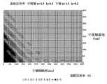
ここで、図2にレジスト中間層膜のk値(消衰係数)を変化させたときの基板反射率を示す。
レジスト中間層膜のk値として0.2以下の低い値と、適切な膜厚設定によって、1%以下の十分な反射防止効果を得ることができる。Here, FIG. 2 shows the substrate reflectance when the k value (extinction coefficient) of the resist intermediate layer film is changed.
By setting the k value of the resist intermediate layer film to a low value of 0.2 or less and setting the film thickness appropriately, a sufficient antireflection effect of 1% or less can be obtained.
図3及び図4は、下層膜のk値が0.2の場合と0.6の場合の、中間層と下層の膜厚を変化させたときの反射率変化を示す。レジスト下層膜のk値が高い方(0.6の場合(図4))が、より薄膜で反射を1%以下に抑えることができる。レジスト下層膜のk値が0.2の場合(図3)、膜厚250nmでは反射を1%にするためにレジスト中間層膜の膜厚を厚くしなければならない。レジスト中間層膜の膜厚を上げると、レジスト中間層膜を加工するときのドライエッチング時に最上層のレジストに対する負荷が大きく、好ましいことではない。図3及び図4は、露光装置のレンズのNAが0.85のドライ露光の場合の反射であるが、3層プロセスの中間層のn値(屈折率)、k値と膜厚を最適化することによって、下層膜のk値によらずに1%以下の反射率にすることができることが示されている。 FIGS. 3 and 4 show changes in reflectance when the film thicknesses of the intermediate layer and the lower layer are changed when the k value of the lower layer film is 0.2 and 0.6. The higher the k value of the resist underlayer film (when it is 0.6 (FIG. 4)), the reflection can be suppressed to 1% or less with a thinner film. When the k value of the resist underlayer film is 0.2 (FIG. 3), the film thickness of the resist intermediate layer film must be increased in order to make
ところが、液浸リソグラフィーによって投影レンズのNAが1.0を超え、レジストだけでなくレジストの下の反射防止膜に入射する光の角度が浅くなってきている。反射防止膜は、膜自体の吸収だけでなく、光の干渉効果による打ち消しの作用を用いて反射を抑えている。斜めの光は光の干渉効果が小さくなるため、反射が増大する。 However, due to the immersion lithography, the NA of the projection lens exceeds 1.0, and the angle of light entering not only the resist but also the antireflection film under the resist is becoming shallow. The antireflection film not only absorbs the film itself, but also suppresses reflection by using the canceling action due to the interference effect of light. Since the oblique light has a smaller light interference effect, reflection increases.
3層プロセスの膜の中で光の干渉作用を用いて反射防止を行っているのは中間層である。下層膜は干渉作用を用いるには十分に厚いために干渉効果による打ち消し合いによる反射防止効果はない。下層膜表面からの反射を抑える必要があり、そのためにはk値を0.6より小さく、n値を上層の中間層に近い値にしなければならない。k値が小さすぎて透明性が高すぎると、基板からの反射も生じてくるため、液浸露光のNA1.3の場合、k値は0.25〜0.48程度が最適となる。n値は中間層、下層共にレジストのn値1.7に近い値が目標値となる。特に好ましいn値・k値の組合せはn/k=1.50/0.30〜0.35程度とされている。 In the film of the three-layer process, it is the intermediate layer that performs antireflection by using the interference effect of light. Since the lower layer film is thick enough to use the interference effect, there is no antireflection effect due to cancellation due to the interference effect. It is necessary to suppress reflection from the surface of the lower layer film, and for that purpose, the k value must be smaller than 0.6 and the n value must be close to the upper intermediate layer. If the k value is too small and the transparency is too high, reflection from the substrate also occurs. Therefore, in the case of NA1.3 for immersion exposure, the optimum k value is about 0.25 to 0.48. The target value of the n value is close to the resist n value of 1.7 for both the intermediate layer and the lower layer. A particularly preferable combination of n value and k value is about n/k=1.50/0.30 to 0.35.
加工線幅の縮小に伴い、下層膜をマスクに被加工基板をエッチングするときに下層膜がよれたり曲がったりする現象が起きる事が報告されている(非特許文献1)。CVDで作成したアモルファスカーボン(以後「CVD−C」とする)膜は、膜中の水素原子を極めて少なくすることができ、よれ防止には非常に有効であることは、一般的によく知られている。 It has been reported that when the processing line width is reduced, a phenomenon in which the lower layer film is twisted or bent occurs when the substrate to be processed is etched using the lower layer film as a mask (Non-Patent Document 1). It is generally well known that an amorphous carbon (hereinafter referred to as “CVD-C”) film formed by CVD can extremely reduce the number of hydrogen atoms in the film and is very effective in preventing the kinking. ing.
しかしながら、下地の被加工基板に段差がある場合、下層膜によって段差を平坦化させる必要がある。下層膜を平坦化させることによって、その上に成膜する中間層やフォトレジストの膜厚変動を抑え、リソグラフィーのフォーカスマージンを拡大することができる。
メタンガス、エタンガス、アセチレンガス等を原料に用いたCVD−C膜は、段差をフラットに埋め込むことが困難である。一方、下層膜をスピンコーティングによって形成した場合、基板の凹凸を埋め込むことができる長所がある。However, when the underlying substrate to be processed has a step, it is necessary to flatten the step by the lower layer film. By flattening the lower layer film, it is possible to suppress fluctuations in the film thickness of the intermediate layer and the photoresist formed thereon, and to expand the focus margin of lithography.
In the CVD-C film using methane gas, ethane gas, acetylene gas, etc. as a raw material, it is difficult to bury the steps flat. On the other hand, when the lower layer film is formed by spin coating, there is an advantage that irregularities of the substrate can be embedded.
このように、CVD−C膜は段差の埋め込み特性が悪く、またCVD装置の価格と装置フットプリント面積の占有により導入が困難な場合がある。スピンコート法で成膜可能な下層膜材料でよれの問題を解決することができれば、プロセスと装置の簡略化のメリットは大きい。
そのため、反射防止膜としての最適なn、k値と埋め込み特性、優れたパターン曲がり耐性を有し、エッチング中のよれが生じない下層膜材料及び下層膜を形成するための方法が求められている。As described above, the CVD-C film has a poor step-filling property, and it may be difficult to introduce the CVD-C film due to the cost of the CVD apparatus and the footprint of the apparatus. If the problem of the twist can be solved by the lower layer film material that can be formed by the spin coating method, the merit of simplification of the process and the device is great.
Therefore, there is a demand for a method for forming an underlayer film material and an underlayer film that have optimum n and k values as an antireflection film, burying characteristics, excellent pattern bending resistance, and do not cause wrinkling during etching. ..
本発明は上記事情に鑑みなされたもので、特には3層レジストプロセス用下層膜として反射率を低減でき、パターン曲がり耐性が高く、特には60nmよりも細い高アスペクトラインにおけるエッチング後のラインの倒れやよれの発生がない下層膜を形成できるレジスト下層膜形成用組成物、及びこれを用いたパターン形成方法を提供することを目的とする。 The present invention has been made in view of the above circumstances, and in particular, as a lower layer film for a three-layer resist process, the reflectance can be reduced, the pattern bending resistance is high, and particularly, the line collapse after etching in a high aspect line thinner than 60 nm. An object of the present invention is to provide a composition for forming a resist underlayer film which can form an underlayer film free from kinking, and a pattern forming method using the same.
上記課題を解決するため、本発明は、下記一般式(1)で示される化合物及び該化合物の縮合体のいずれかもしくは両方と、有機溶剤とを含有するレジスト下層膜形成用組成物を提供する。
このようなものを用いて形成されたレジスト下層膜であれば、反射率を低減でき、パターン曲がり耐性が高く、特には60nmよりも細い高アスペクトラインにおけるエッチング後のラインの倒れやよれの発生がないものとなる。 A resist underlayer film formed using such a material can reduce the reflectance and has high resistance to pattern bending, and in particular, the occurrence of line collapse or wrinkling after etching in a high aspect line thinner than 60 nm. There will be nothing.
このとき、前記縮合体として、前記一般式(1)で示される化合物の1種以上に対して、下記一般式(2−1)で示される化合物、下記一般式(2−2)で示される化合物、トリオキサン、パラホルムアルデヒド、フルオレノンから選択される1種以上を作用させることにより得られる縮合体を含有するものであることが好ましい。
このようなレジスト下層膜形成用組成物であれば、本発明の効果をより一層向上させることができる。 With such a resist underlayer film forming composition, the effects of the present invention can be further improved.
またこのとき、前記縮合体として、さらに、下記一般式(3−1)、(3−2)、(3−3)、(3−4)、(3−5)で示される化合物のうちから選択される1種以上を作用させることにより得られる縮合体を含有するものであることが好ましい。
このようなものを組み合わせることで、n値、k値及びエッチング耐性を制御することができる。 By combining such materials, the n value, k value and etching resistance can be controlled.
またこのとき、前記レジスト下層膜形成用組成物が、前記縮合体に含まれる水素原子の一部をグリシジル基に置換した縮合体を含有することが好ましい。 At this time, it is preferable that the resist underlayer film forming composition contains a condensate in which a part of hydrogen atoms contained in the condensate is replaced with a glycidyl group.
このように、本発明のレジスト下層膜形成用組成物は、前記縮合体に含まれる水素原子の一部をグリシジル基に置換した縮合体を含有することもできる。 Thus, the composition for forming a resist underlayer film of the present invention may contain a condensate in which a part of hydrogen atoms contained in the condensate is replaced with a glycidyl group.
またこのとき、前記レジスト下層膜形成用組成物が、前記一般式(1)で示される化合物、該化合物の縮合体、該縮合体に含まれる水素原子の一部をグリシジル基に置換した縮合体のうちから選択される2種以上を含有することが好ましい。 At this time, the composition for forming a resist underlayer film is a compound represented by the general formula (1), a condensate of the compound, or a condensate in which a part of hydrogen atoms contained in the condensate is replaced with a glycidyl group. It is preferable to contain two or more selected from the above.
このようなレジスト下層膜形成用組成物を用いて形成されるレジスト下層膜であれば、特に短波長の露光に対して、優れた反射防止膜として機能し、即ち透明性が高く、最適なn値、k値を有し、さらに基板加工時におけるパターン曲がり耐性に優れたものとなる。 A resist underlayer film formed using such a resist underlayer film forming composition functions as an excellent antireflection film particularly for exposure to short wavelengths, that is, it has high transparency and has an optimum n value. Value and k value, and further has excellent resistance to pattern bending during substrate processing.
またこのとき、前記レジスト下層膜形成用組成物が、架橋剤又は酸発生剤もしくはこれらの両方を含有するものであることが好ましい。 At this time, it is preferable that the resist underlayer film forming composition contains a crosslinking agent, an acid generator, or both of them.
このように、本発明のレジスト下層膜形成用組成物が、さらに架橋剤又は酸発生剤もしくはこれらの両方を含有することで、基板等への塗布後にベーク等により、レジスト下層膜内での架橋反応を促進することができる。従って、このようなレジスト下層膜は、レジスト上層膜とのインターミキシングの恐れが少なく、レジスト上層膜への低分子成分の拡散が少ないものとなる。 Thus, the composition for forming a resist underlayer film of the present invention further contains a cross-linking agent or an acid generator, or both of them, so that the resist under-layer film is cross-linked by baking after coating onto a substrate or the like. The reaction can be accelerated. Therefore, such a resist lower layer film has less risk of intermixing with the resist upper layer film, and less diffusion of low molecular components into the resist upper layer film.
また、本発明では、被加工体上に前記レジスト下層膜形成用組成物を用いてレジスト下層膜を形成し、該レジスト下層膜の上にケイ素原子を含有するレジスト中間層膜材料を用いてレジスト中間層膜を形成し、該レジスト中間層膜の上にフォトレジスト組成物のレジスト上層膜材料を用いてレジスト上層膜を形成し、該レジスト上層膜に回路パターンを形成し、該パターンが形成されたレジスト上層膜をマスクにしてレジスト中間層膜をエッチングし、該パターンが形成されたレジスト中間層膜をマスクにしてレジスト下層膜をエッチングし、さらに、該パターンが形成されたレジスト下層膜をマスクにして被加工体をエッチングして該被加工体にパターンを形成するパターン形成方法を提供する。 Further, in the present invention, a resist underlayer film is formed on the object to be processed by using the resist underlayer film forming composition, and a resist intermediate layer film material containing a silicon atom is formed on the resist underlayer film. An intermediate layer film is formed, a resist upper layer film is formed on the resist intermediate layer film using a resist upper layer film material of a photoresist composition, a circuit pattern is formed on the resist upper layer film, and the pattern is formed. The resist intermediate layer film is etched using the resist upper layer film as a mask, the resist intermediate layer film having the pattern is used as a mask, the resist lower layer film is etched, and the resist lower layer film having the pattern is masked There is provided a pattern forming method for forming a pattern on an object to be processed by etching the object to be processed.
このように、本発明のレジスト下層膜形成用組成物を用いてパターン形成を行うと、被加工体にレジスト上層膜のパターンを高精度で転写、形成することが可能になる。 As described above, when a pattern is formed using the composition for forming a resist lower layer film of the present invention, it becomes possible to transfer and form a pattern of a resist upper layer film on a workpiece with high accuracy.
また、本発明では、被加工体上に前記レジスト下層膜形成用組成物を用いてレジスト下層膜を形成し、該レジスト下層膜の上にケイ素原子を含有するレジスト中間層膜材料を用いてレジスト中間層膜を形成し、該レジスト中間層膜の上に有機反射防止膜(BARC)を形成し、該BARC上にフォトレジスト組成物のレジスト上層膜材料を用いてレジスト上層膜を形成して4層レジスト膜とし、該レジスト上層膜に回路パターンを形成し、該パターンが形成されたレジスト上層膜をマスクにしてBARC膜とレジスト中間層膜をエッチングし、該パターンが形成されたレジスト中間膜をマスクにしてレジスト下層膜をエッチングし、さらに、該パターンが形成されたレジスト下層膜をマスクにして被加工体をエッチングして該被加工体にパターンを形成するパターン形成方法を提供する。 Further, in the present invention, a resist underlayer film is formed on the object to be processed by using the resist underlayer film forming composition, and a resist intermediate layer film material containing a silicon atom is formed on the resist underlayer film. An intermediate layer film is formed, an organic antireflection film (BARC) is formed on the resist intermediate layer film, and a resist upper layer film of a photoresist composition is used to form a resist upper layer film on the BARC. As a layer resist film, a circuit pattern is formed on the resist upper layer film, the BARC film and the resist intermediate layer film are etched using the resist upper layer film having the pattern as a mask, and the resist intermediate film having the pattern is formed. Provided is a pattern forming method for etching a resist underlayer film using a mask, and further for etching a processed object using the resist underlayer film having the pattern formed as a mask to form a pattern on the processed object.
このように、本発明のパターン形成方法では、レジスト中間層膜とレジスト上層膜の間にBARCを形成することができる。 As described above, according to the pattern forming method of the present invention, BARC can be formed between the resist intermediate layer film and the resist upper layer film.
また、本発明では、被加工体上に前記レジスト下層膜形成用組成物を用いてレジスト下層膜を形成し、該レジスト下層膜の上にケイ素酸化膜、ケイ素窒化膜、ケイ素酸化窒化膜から選ばれる無機ハードマスク中間層膜を形成し、該無機ハードマスク中間層膜の上にフォトレジスト組成物のレジスト上層膜材料を用いてレジスト上層膜を形成して、該レジスト上層膜に回路パターンを形成し、該パターンが形成されたレジスト上層膜をマスクにして無機ハードマスク中間層膜をエッチングし、該パターンが形成された無機ハードマスク中間層膜をマスクにしてレジスト下層膜をエッチングし、さらに、該パターンが形成されたレジスト下層膜をマスクにして被加工体をエッチングして該被加工体にパターンを形成するパターン形成方法を提供する。 Further, in the present invention, a resist underlayer film is formed on the object to be processed using the resist underlayer film forming composition, and a silicon oxide film, a silicon nitride film, or a silicon oxynitride film is selected on the resist underlayer film. Forming an inorganic hard mask intermediate layer film, forming a resist upper layer film on the inorganic hard mask intermediate layer film using a resist upper layer film material of a photoresist composition, and forming a circuit pattern on the resist upper layer film. Then, the inorganic hard mask intermediate layer film is etched by using the resist upper layer film having the pattern as a mask, and the resist lower layer film is etched by using the inorganic hard mask intermediate layer film having the pattern as a mask. Provided is a pattern forming method for forming a pattern on an object to be processed by etching the object to be processed using the resist underlayer film on which the pattern is formed as a mask.
このように、本発明のパターン形成方法では、無機ハードマスク中間層膜を用いた場合にも、本発明のレジスト下層膜形成用組成物を用いてパターンを形成することにより、高精度で被加工体にパターンを形成することができる。 As described above, in the pattern forming method of the present invention, even when an inorganic hard mask intermediate layer film is used, a pattern is formed by using the resist underlayer film forming composition of the present invention, so that it is processed with high accuracy. Patterns can be formed on the body.
さらに、本発明では、被加工体上に前記レジスト下層膜形成用組成物を用いてレジスト下層膜を形成し、該レジスト下層膜の上にケイ素酸化膜、ケイ素窒化膜、ケイ素酸化窒化膜から選ばれる無機ハードマスク中間層膜を形成し、該無機ハードマスク中間層膜の上に有機反射防止膜(BARC)を形成し、該BARC上にフォトレジスト組成物のレジスト上層膜材料を用いてレジスト上層膜を形成して4層レジスト膜とし、該レジスト上層膜に回路パターンを形成し、該パターンが形成されたレジスト上層膜をマスクにしてBARC膜と無機ハードマスク中間層膜をエッチングし、該パターンが形成された無機ハードマスク中間層膜をマスクにしてレジスト下層膜をエッチングし、さらに、該パターンが形成されたレジスト下層膜をマスクにして被加工体をエッチングして該被加工体にパターンを形成するパターン形成方法を提供する。 Further, in the present invention, a resist underlayer film is formed on the object to be processed using the composition for forming a resist underlayer film, and a silicon oxide film, a silicon nitride film, or a silicon oxynitride film is selected on the resist underlayer film. Forming an inorganic hard mask intermediate layer film, forming an organic antireflection film (BARC) on the inorganic hard mask intermediate layer film, and using a resist upper layer film material of a photoresist composition on the BARC. A film is formed into a four-layer resist film, a circuit pattern is formed on the resist upper layer film, and the BARC film and the inorganic hard mask intermediate layer film are etched using the resist upper layer film on which the pattern is formed as a mask to form the pattern. The resist underlayer film is etched by using the formed inorganic hard mask intermediate layer film as a mask, and the object is etched by using the resist underlayer film having the pattern formed as a mask to form a pattern on the object. A pattern forming method for forming is provided.
このように、ハードマスク中間層膜の上にBARCを形成すれば、2層の反射防止膜によって、1.0を超える高NAの液浸露光においても反射を抑えることが可能となる。また、ハードマスク中間層膜上のフォトレジストパターンの裾引きを低減させる効果もある。 As described above, when BARC is formed on the hard mask intermediate layer film, the two-layer antireflection film can suppress the reflection even in the immersion exposure with a high NA exceeding 1.0. It also has the effect of reducing the bottoming of the photoresist pattern on the hard mask intermediate layer film.
このとき、前記無機ハードマスク中間層膜を、CVD法又はALD法によって形成することができる。
このように、無機ハードマスク中間層膜を、CVD法又はALD法により形成することにより、エッチング耐性を高くすることができる。At this time, the inorganic hard mask intermediate layer film can be formed by a CVD method or an ALD method.
As described above, by forming the inorganic hard mask intermediate layer film by the CVD method or the ALD method, the etching resistance can be increased.
また、前記レジスト上層膜のパターン形成方法を、波長が10nm以上300nm以下の光リソグラフィー、電子線による直接描画、ナノインプリンティング又はこれらの組み合わせによるパターン形成とすることができる。 The pattern formation method of the resist upper layer film may be pattern formation by photolithography having a wavelength of 10 nm or more and 300 nm or less, direct writing with an electron beam, nanoimprinting, or a combination thereof.
このように、波長が10nm以上300nm以下の光リソグラフィー、電子線による直接描画、ナノインプリンティング又はこれらの組み合わせにより、レジスト上層膜にパターンを形成することができる。 Thus, the pattern can be formed on the resist upper layer film by photolithography with a wavelength of 10 nm or more and 300 nm or less, direct writing with an electron beam, nanoimprinting, or a combination thereof.
また、前記パターン形成方法における現像方法を、アルカリ現像又は有機溶剤による現像とすることができる。
このように、本発明では、アルカリ現像又は有機溶剤による現像を適用することができる。Further, the developing method in the pattern forming method may be alkali developing or organic solvent developing.
Thus, in the present invention, alkali development or development with an organic solvent can be applied.
また、前記被加工体として、半導体装置基板、又は半導体装置基板に、金属膜、金属炭化膜、金属酸化膜、金属窒化膜、金属酸化炭化膜、及び金属酸化窒化膜のいずれかが成膜されたものを用いることが好ましい。
この場合、前記金属として、ケイ素、チタン、タングステン、ハフニウム、ジルコニウム、クロム、ゲルマニウム、銅、銀、金、アルミニウム、インジウム、ガリウム、ヒ素、パラジウム、鉄、タンタル、イリジウム、モリブデン又はこれらの合金を用いることができる。As the workpiece, a semiconductor device substrate, or any one of a metal film, a metal carbide film, a metal oxide film, a metal nitride film, a metal oxycarbide film, and a metal oxynitride film is formed on the semiconductor device substrate. It is preferable to use the one.
In this case, as the metal, silicon, titanium, tungsten, hafnium, zirconium, chromium, germanium, copper, silver, gold, aluminum, indium, gallium, arsenic, palladium, iron, tantalum, iridium, molybdenum or an alloy thereof is used. be able to.
このように、本発明では、前記被加工体及び前記金属として、上記のようなものを用いることができる。 As described above, in the present invention, the above-mentioned objects can be used as the workpiece and the metal.
上述のように、本発明のレジスト下層膜形成用組成物を用いて形成したレジスト下層膜であれば、反射率を低減でき、即ち反射防止膜としての最適なn値、k値を有し、かつ、強固なものとなり、基板加工時におけるパターン曲がり耐性に優れ、特には60nmよりも細い高アスペクトラインにおけるエッチング後のラインの倒れやよれの発生がないものとなる。
また、本発明のパターン形成方法であれば、被加工体にレジスト上層膜のパターンを高精度で転写、形成することが可能になる。As described above, the resist underlayer film formed using the composition for forming a resist underlayer film of the present invention can reduce the reflectance, that is, has the optimum n value and k value as an antireflection film, In addition, it becomes strong and has excellent resistance to pattern bending during substrate processing, and in particular, there is no occurrence of tipping or wrinkling of lines after etching in high aspect lines thinner than 60 nm.
Further, according to the pattern forming method of the present invention, it becomes possible to transfer and form the pattern of the resist upper layer film on the object to be processed with high accuracy.
上述のように、パターン曲がり耐性が高く、特には60nmよりも細い高アスペクトラインにおけるエッチング後のラインの倒れやよれの発生がない多層レジストプロセス用下層膜を形成できるレジスト下層膜形成用組成物、及びこれを用いたパターン形成方法が求められていた。 As described above, a composition for forming a resist underlayer film, which has a high pattern bending resistance, and is capable of forming an underlayer film for a multilayer resist process without occurrence of line collapse or wrinkling after etching particularly in a high aspect line thinner than 60 nm, And the pattern formation method using this was calculated|required.
本発明者らは、上記課題について鋭意検討を重ねた結果、剛直な構造を有するジベンゾクリセン骨格を含有する化合物やその縮合体を含有するレジスト下層膜形成用組成物から得られるレジスト下層膜は、エッチング後のラインの倒れやよれの発生が見られないだけでなく、適切な反射制御可能な光学特性を有することを見出し、本発明を完成させた。 The present inventors have conducted extensive studies on the above problems, and a resist underlayer film obtained from a resist underlayer film-forming composition containing a compound containing a dibenzochrysene skeleton having a rigid structure or a condensate thereof is The present invention has been completed by finding that not only the occurrence of line collapse and wrinkling after etching is not observed, but also that the film has suitable reflection controllable optical characteristics.
即ち、本発明は、下記一般式(1)で示される化合物及び該化合物の縮合体のいずれかもしくは両方と、有機溶剤とを含有するレジスト下層膜形成用組成物である。
以下、本発明の実施の形態について説明するが、本発明はこれらに限定されるものではない。 Hereinafter, embodiments of the present invention will be described, but the present invention is not limited thereto.
本発明のレジスト下層膜形成用組成物は、下記一般式(1)で示される化合物及び該化合物の縮合体のいずれかもしくは両方を含有する。
ここで、上記一般式(1)で示される化合物としては、具体的には下記のものを挙げることができる。
また、本発明のレジスト下層膜形成用組成物は、前記縮合体として、前記一般式(1)で示される化合物の1種以上に対して、下記一般式(2−1)で示される化合物、下記一般式(2−2)で示される化合物、トリオキサン、パラホルムアルデヒド、フルオレノンから選択される1種以上を作用させることにより得られる縮合体を含有するものであることが好ましい。
ここで、一般式(2−1)で示されるアルデヒド化合物としては、具体的には、ホルムアルデヒド、フルフリルアルデヒド、ベンズアルデヒド、ナフトアルデヒド、p−ヒドロキシベンズアルデヒド、特開2012−098431号公報、特開2012−118300号公報、特開2012−145897号公報に記載されているものを例示できる。 Here, as the aldehyde compound represented by the general formula (2-1), specifically, formaldehyde, furfuryl aldehyde, benzaldehyde, naphthaldehyde, p-hydroxybenzaldehyde, JP 2012-098431 A, JP 2012 A and JP 2012 A are disclosed. Examples include those described in JP-A-118300 and JP 2012-145897.
また、上記一般式(2−1)の等価体を使用することもできる。例えば、上記一般式(2−1)の等価体としては、下記一般式
又は、ホルミル基のα−炭素原子に水素原子が結合している場合は、
等を例示できる。例えば、トリオキサンやパラホルムアルデヒドはホルムアルデヒドの等価体である。Further, an equivalent body of the above general formula (2-1) can also be used. For example, as an equivalent body of the above general formula (2-1),
Alternatively, when a hydrogen atom is bonded to the α-carbon atom of the formyl group,
Etc. can be illustrated. For example, trioxane and paraformaldehyde are formaldehyde equivalents.
ここで、一般式(2−2)で示される化合物としては、具体的には以下の化合物を例示できる。
また、本発明のレジスト下層膜形成用組成物は、前記縮合体として、さらに、下記一般式(3−1)、(3−2)、(3−3)、(3−4)、(3−5)で示される化合物のうちから選択される1種以上を作用させることにより得られる縮合体を含有するものであることが好ましい。
上記一般式(3−1)で示される化合物としては、例えば、1−メチルナフタレン、2−メチルナフタレン、1,3−ジメチルナフタレン、1,5−ジメチルナフタレン、1,7−ジメチルナフタレン、2,7−ジメチルナフタレン、2−ビニルナフタレン、2,6−ジビニルナフタレン、アセナフテン、アセナフチレン、アントラセン、1−メトキシナフタレン、2−メトキシナフタレン、1,4−ジメトキシナフタレン、2,7−ジメトキシナフタレン、1−ナフトール、2−ナフトール、2−メチル−1−ナフトール、4−メトキシ−1−ナフトール、7−メトキシ−2−ナフトール、1,2−ジヒドロキシナフタレン、1,3−ジヒドロキシナフタレン、2,3−ジヒドロキシナフタレン、1,4−ジヒドロキシナフタレン、1,5−ジヒドロキシナフタレン、1,6−ジヒドロキシナフタレン、2,6−ジヒドロキシナフタレン、1,7−ジヒドロキシナフタレン、2,7−ジヒドロキシナフタレン、1,8−ジヒドロキシナフタレン、5−アミノ−1−ナフトール、2−メトキシカルボニル−1−ナフトール、1−(4−ヒドロキシフェニル)ナフタレン、6−(4−ヒドロキシフェニル)−2−ナフトール、6−(シクロヘキシル)−2−ナフトール、1,1’−ビ−2,2’−ナフトール、6,6’−ビ−2,2’−ナフトール、9,9−ビス(6−ヒドロキシ−2−ナフチル)フルオレン、6−ヒドロキシ−2−ビニルナフタレン、1−ヒドロキシメチルナフタレン、2−ヒドロキシメチルナフタレン、1−グリシドキシナフタレン、2−グリシドキシナフタレン、1,3−ジグリシドキシナフタレン、1,5−ジグリシドキシナフタレン、1,7−ジグリシドキシナフタレン、2,7−ジグリシドキシナフタレン等を挙げることができる。 Examples of the compound represented by the general formula (3-1) include 1-methylnaphthalene, 2-methylnaphthalene, 1,3-dimethylnaphthalene, 1,5-dimethylnaphthalene, 1,7-dimethylnaphthalene, 2, 7-dimethylnaphthalene, 2-vinylnaphthalene, 2,6-divinylnaphthalene, acenaphthene, acenaphthylene, anthracene, 1-methoxynaphthalene, 2-methoxynaphthalene, 1,4-dimethoxynaphthalene, 2,7-dimethoxynaphthalene, 1-naphthol , 2-naphthol, 2-methyl-1-naphthol, 4-methoxy-1-naphthol, 7-methoxy-2-naphthol, 1,2-dihydroxynaphthalene, 1,3-dihydroxynaphthalene, 2,3-dihydroxynaphthalene, 1,4-dihydroxynaphthalene, 1,5-dihydroxynaphthalene, 1,6-dihydroxynaphthalene, 2,6-dihydroxynaphthalene, 1,7-dihydroxynaphthalene, 2,7-dihydroxynaphthalene, 1,8-dihydroxynaphthalene, 5 -Amino-1-naphthol, 2-methoxycarbonyl-1-naphthol, 1-(4-hydroxyphenyl)naphthalene, 6-(4-hydroxyphenyl)-2-naphthol, 6-(cyclohexyl)-2-naphthol, 1 ,1'-bi-2,2'-naphthol, 6,6'-bi-2,2'-naphthol, 9,9-bis(6-hydroxy-2-naphthyl)fluorene, 6-hydroxy-2-vinyl Naphthalene, 1-hydroxymethylnaphthalene, 2-hydroxymethylnaphthalene, 1-glycidoxynaphthalene, 2-glycidoxynaphthalene, 1,3-diglycidoxynaphthalene, 1,5-diglycidoxynaphthalene, 1,7- Examples thereof include diglycidoxynaphthalene and 2,7-diglycidoxynaphthalene.
上記一般式(3−2)で示される化合物としては、例えば、トルエン、o−キシレン、m−キシレン、p−キシレン、クメン、インダン、インデン、メシチレン、ビフェニール、フルオレン、フェノール、アニソール、o−クレゾール、m−クレゾール、p−クレゾール、2,3−ジメチルフェノール、2,5−ジメチルフェノール、3,4−ジメチルフェノール、3,5−ジメチルフェノール、2,4−ジメチルフェノール、2,6−ジメチルフェノール、2,3,5−トリメチルフェノール、3,4,5−トリメチルフェノール、2−t−ブチルフェノール、3−t−ブチルフェノール、4−t−ブチルフェノール、レゾルシノール、2−メチルレゾルシノール、4−メチルレゾルシノール、5−メチルレゾルシノール、カテコール、4−t−ブチルカテコール、2−メトキシフェノール、3−メトキシフェノール、2−プロピルフェノール、3−プロピルフェノール、4−プロピルフェノール、2−イソプロピルフェノール、3−イソプロピルフェノール、4−イソプロピルフェノール、2−メトキシ−5−メチルフェノール、2−t−ブチル−5−メチルフェノール、4−フェニルフェノール、トリチルフェノール、ピロガロール、チモール、フェニルグリシジルエーテル、4−フルオロフェノール、3,4−ジフルオロフェノール、4−トリフルオロメチルフェノール、4−クロロフェノール、9,9−ビス(4−ヒドロキシフェニル)フルオレン、スチレン、4−t−ブトキシスチレン、4−アセトキシスチレン、4−メトキシスチレン、ジビニルベンゼン、ベンジルアルコール等を挙げることができる。 Examples of the compound represented by the general formula (3-2) include toluene, o-xylene, m-xylene, p-xylene, cumene, indane, indene, mesitylene, biphenyl, fluorene, phenol, anisole and o-cresol. , M-cresol, p-cresol, 2,3-dimethylphenol, 2,5-dimethylphenol, 3,4-dimethylphenol, 3,5-dimethylphenol, 2,4-dimethylphenol, 2,6-dimethylphenol , 2,3,5-trimethylphenol, 3,4,5-trimethylphenol, 2-t-butylphenol, 3-t-butylphenol, 4-t-butylphenol, resorcinol, 2-methylresorcinol, 4-methylresorcinol, 5 -Methylresorcinol, catechol, 4-t-butylcatechol, 2-methoxyphenol, 3-methoxyphenol, 2-propylphenol, 3-propylphenol, 4-propylphenol, 2-isopropylphenol, 3-isopropylphenol, 4- Isopropylphenol, 2-methoxy-5-methylphenol, 2-t-butyl-5-methylphenol, 4-phenylphenol, tritylphenol, pyrogallol, thymol, phenylglycidyl ether, 4-fluorophenol, 3,4-difluorophenol , 4-trifluoromethylphenol, 4-chlorophenol, 9,9-bis(4-hydroxyphenyl)fluorene, styrene, 4-t-butoxystyrene, 4-acetoxystyrene, 4-methoxystyrene, divinylbenzene, benzyl alcohol. Etc. can be mentioned.
上記一般式(3−3)で示される化合物としては、具体的には、下記のものを例示できる。
上記一般式(3−4)で示される化合物としては、具体的には、下記のものを例示できる。
上記一般式(3−5)で示される化合物としては、具体的には、下記のものを例示できる。
なお、上記一般式(3−1)、(3−2)、(3−3)、(3−4)、(3−5)で示される化合物は、それぞれ単独で使用してもよいし、n値、k値及びエッチング耐性を制御するため、2種類以上を組み合わせて上記一般式(1)で示される化合物の1種以上に対して作用させてもよい。また、これらを上記一般式(2−1)で示される化合物、上記一般式(2−2)で示される化合物、トリオキサン、パラホルムアルデヒド、フルオレノンから選択される1種以上とともに、上記一般式(1)で示される化合物の1種以上に対して作用させてもよい。 The compounds represented by the general formulas (3-1), (3-2), (3-3), (3-4) and (3-5) may be used alone, In order to control the n value, k value and etching resistance, two or more kinds may be combined and acted on one or more compounds represented by the general formula (1). Further, these are combined with one or more compounds selected from the compound represented by the general formula (2-1), the compound represented by the general formula (2-2), trioxane, paraformaldehyde, and fluorenone, together with the general formula (1 ), and may act on one or more compounds represented by
また、本発明のレジスト下層膜形成用組成物は、前記縮合体に含まれる水素原子の一部をグリシジル基に置換した縮合体を含有することができる。 Further, the resist underlayer film forming composition of the present invention may contain a condensate in which a part of hydrogen atoms contained in the condensate is replaced with a glycidyl group.
さらに、本発明のレジスト下層膜形成用組成物は、前記一般式(1)で示される化合物、該化合物の縮合体、該縮合体に含まれる水素原子の一部をグリシジル基に置換した縮合体のうちから選択される2種以上を含有することが好ましい。 Furthermore, the composition for forming a resist underlayer film of the present invention is a compound represented by the general formula (1), a condensate of the compound, or a condensate in which a part of hydrogen atoms contained in the condensate is replaced with a glycidyl group. It is preferable to contain two or more selected from the above.
上記のような原料を使用して重縮合反応で得られる縮合体は、通常、無溶媒又は溶媒中で酸又は塩基を触媒として用いて、室温又は必要に応じて冷却又は加熱下で得ることができる。 The condensate obtained by the polycondensation reaction using the raw materials as described above can be usually obtained without solvent or in a solvent using an acid or a base as a catalyst at room temperature or under cooling or heating as necessary. it can.
用いられる溶媒としては、具体的には、メタノール、エタノール、イソプロピルアルコール、ブタノール、エチレングリコール、プロピレングリコール、ジエチレングリコール、グリセロール、メチルセロソルブ、エチルセロソルブ、ブチルセロソルブ、プロピレングリコールモノメチルエーテル等のアルコール類、ジエチルエーテル、ジブチルエーテル、ジエチレングリコールジエチルエーテル、ジエチレングリコールジメチルエーテル、テトラヒドロフラン、1,4−ジオキサン等のエーテル類、塩化メチレン、クロロフォルム、ジクロロエタン、トリクロロエチレン等の塩素系溶剤類、ヘキサン、ヘプタン、ベンゼン、トルエン、キシレン、クメン等の炭化水素類、アセトニトリル等のニトリル類、アセトン、エチルメチルケトン、イソブチルメチルケトン等のケトン類、酢酸エチル、酢酸n−ブチル、プロピレングリコールメチルエーテルアセテート等のエステル類、γ−ブチロラクトン等のラクトン類、ジメチルスルホキシド、N,N−ジメチルホルムアミド、ヘキサメチルホスホリックトリアミド等の非プロトン性極性溶媒類が例示でき、これらを単独あるいは2種類以上を混合して用いることができる。これらの溶媒は、反応原料100質量部に対して0〜2,000質量部の範囲で使用できる。 As the solvent used, specifically, alcohols such as methanol, ethanol, isopropyl alcohol, butanol, ethylene glycol, propylene glycol, diethylene glycol, glycerol, methyl cellosolve, ethyl cellosolve, butyl cellosolve, propylene glycol monomethyl ether, diethyl ether, Ethers such as dibutyl ether, diethylene glycol diethyl ether, diethylene glycol dimethyl ether, tetrahydrofuran, 1,4-dioxane, chlorinated solvents such as methylene chloride, chloroform, dichloroethane, trichloroethylene, hexane, heptane, benzene, toluene, xylene, cumene, etc. Hydrocarbons, nitriles such as acetonitrile, ketones such as acetone, ethyl methyl ketone and isobutyl methyl ketone, esters such as ethyl acetate, n-butyl acetate and propylene glycol methyl ether acetate, lactones such as γ-butyrolactone, Aprotic polar solvents such as dimethyl sulfoxide, N,N-dimethylformamide and hexamethylphosphoric triamide can be exemplified, and these can be used alone or in combination of two or more kinds. These solvents can be used in the range of 0 to 2,000 parts by mass with respect to 100 parts by mass of the reaction raw material.
用いられる酸触媒としては、塩酸、臭化水素酸、硫酸、硝酸、リン酸、ヘテロポリ酸等の無機酸類、シュウ酸、トリフルオロ酢酸、メタンスルホン酸、ベンゼンスルホン酸、p−トルエンスルホン酸、トリフルオロメタンスルホン酸等の有機酸類、三塩化アルミニウム、アルミニウムエトキシド、アルミニウムイソプロポキシド、三フッ化ホウ素、三塩化ホウ素、三臭化ホウ素、四塩化錫、四臭化錫、二塩化ジブチル錫、ジブチル錫ジメトキシド、ジブチル錫オキシド、四塩化チタン、四臭化チタン、チタン(IV)メトキシド、チタン(IV)エトキシド、チタン(IV)イソプロポキシド、酸化チタン(IV)等のルイス酸類を用いることができる。 Examples of the acid catalyst used include inorganic acids such as hydrochloric acid, hydrobromic acid, sulfuric acid, nitric acid, phosphoric acid, and heteropoly acid, oxalic acid, trifluoroacetic acid, methanesulfonic acid, benzenesulfonic acid, p-toluenesulfonic acid, trifluoric acid. Organic acids such as methanesulfonic acid, aluminum trichloride, aluminum ethoxide, aluminum isopropoxide, boron trifluoride, boron trichloride, boron tribromide, tin tetrachloride, tin tetrabromide, dibutyltin dichloride, dibutyl Lewis acids such as tin dimethoxide, dibutyltin oxide, titanium tetrachloride, titanium tetrabromide, titanium (IV) methoxide, titanium (IV) ethoxide, titanium (IV) isopropoxide, and titanium (IV) oxide can be used. ..
用いられる塩基触媒としては、具体的には、水酸化ナトリウム、水酸化カリウム、水酸化バリウム、炭酸ナトリウム、炭酸水素ナトリウム、炭酸カリウム、水素化リチウム、水素化ナトリウム、水素化カリウム、水素化カルシウム等の無機塩基類、メチルリチウム、n−ブチルリチウム、塩化メチルマグネシウム、臭化エチルマグネシウム等のアルキル金属類、ナトリウムメトキシド、ナトリウムエトキシド、カリウムt−ブトキシド等のアルコキシド類、トリエチルアミン、ジイソプロピルエチルアミン、N,N−ジメチルアニリン、ピリジン、4−ジメチルアミノピリジン等の有機塩基類を用いることができる。 Specific examples of the base catalyst used include sodium hydroxide, potassium hydroxide, barium hydroxide, sodium carbonate, sodium hydrogen carbonate, potassium carbonate, lithium hydride, sodium hydride, potassium hydride and calcium hydride. Inorganic bases, alkyllithium such as methyllithium, n-butyllithium, methylmagnesium chloride and ethylmagnesium bromide, alkoxides such as sodium methoxide, sodium ethoxide and potassium t-butoxide, triethylamine, diisopropylethylamine, N. , N-dimethylaniline, pyridine, 4-dimethylaminopyridine, and other organic bases can be used.
触媒の使用量は、原料に対して0.001〜100重量%、好ましくは0.005〜50重量%の範囲である。反応温度は−50℃から溶媒の沸点程度が好ましく、室温から100℃がさらに好ましい。 The amount of the catalyst used is in the range of 0.001 to 100% by weight, preferably 0.005 to 50% by weight, based on the raw materials. The reaction temperature is preferably -50°C to the boiling point of the solvent, more preferably room temperature to 100°C.
重縮合反応方法としては、上記の原料となる化合物及び触媒を一括で仕込む方法や、触媒存在下で上記の原料となる化合物を滴下していく方法がある。 As the polycondensation reaction method, there are a method in which the compound as the raw material and the catalyst are charged all at once, and a method in which the compound as the raw material is dropped in the presence of the catalyst.
重縮合反応終了後、系内に存在する未反応原料、触媒等を除去するために、反応釜の温度を130〜230℃にまで上昇させ、1〜50mmHg程度で揮発分を除去する方法や適切な溶媒や水を加えて、縮合体を分画する方法、縮合体を良溶媒に溶解後、貧溶媒中で再沈する方法等、得られた反応生成物の性質により使い分けることができる。 After completion of the polycondensation reaction, in order to remove unreacted raw materials, catalysts, etc. existing in the system, the temperature of the reaction kettle is raised to 130 to 230° C., and a volatile component is removed at about 1 to 50 mmHg. A method of fractionating the condensate by adding a different solvent or water, a method of dissolving the condensate in a good solvent and then reprecipitating in a poor solvent can be used depending on the properties of the obtained reaction product.
このようにして得られた縮合体のポリスチレン換算の分子量は、重量平均分子量(Mw)が500〜500,000、特に1,000〜100,000であることが好ましい。分子量分散度は1.2〜20の範囲内が好ましく用いられるが、モノマー成分、オリゴマー成分又は分子量(Mw)1,000以下の低分子量体をカットすると、ベーク中の揮発成分を抑えることによりベークカップ周辺の汚染や揮発成分の落下による表面欠陥の発生を防ぐことができる。 The polystyrene-equivalent molecular weight of the thus obtained condensate has a weight average molecular weight (Mw) of 500 to 500,000, and particularly preferably 1,000 to 100,000. The molecular weight dispersity is preferably in the range of 1.2 to 20, but when a monomer component, an oligomer component, or a low molecular weight substance having a molecular weight (Mw) of 1,000 or less is cut, the volatile component in the bake is suppressed to prevent baking. It is possible to prevent the occurrence of surface defects due to contamination around the cup and dropping of volatile components.
また、この縮合体には、縮合芳香族、あるいは脂環族の置換基を導入することができる。
ここで導入可能な置換基としては、具体的には下記に挙げることができる。Further, a condensed aromatic or alicyclic substituent can be introduced into this condensate.
Specific examples of the substituent that can be introduced here include the following.
これらの中で、波長248nm露光用には、多環芳香族基、例えばアントラセンメチル基、ピレンメチル基が最も好ましく用いられる。波長193nmでの透明性向上のためには脂環構造を持つものや、ナフタレン構造を持つものが好ましく用いられる。一方、波長157nmにおいてベンゼン環は透明性が向上するウィンドウがあるため、吸収波長をずらして吸収を上げることが好ましい。フラン環はベンゼン環よりも吸収が短波長化して157nmの吸収が若干向上するが、効果は小さい。ナフタレン環やアントラセン環、ピレン環は吸収波長が長波長化することによって吸収が増大し、これらの芳香族環はエッチング耐性も向上する効果もあり、好ましく用いられる。 Of these, polycyclic aromatic groups such as anthracenemethyl group and pyrenemethyl group are most preferably used for exposure at a wavelength of 248 nm. In order to improve transparency at a wavelength of 193 nm, those having an alicyclic structure or those having a naphthalene structure are preferably used. On the other hand, at the wavelength of 157 nm, the benzene ring has a window for improving the transparency, so it is preferable to shift the absorption wavelength to increase the absorption. The absorption of the furan ring is shorter than that of the benzene ring, and the absorption at 157 nm is slightly improved, but the effect is small. The naphthalene ring, the anthracene ring, and the pyrene ring are preferably used because the absorption wavelength increases and the absorption increases, and these aromatic rings also have the effect of improving etching resistance.
置換基の導入方法としては、縮合体に上記置換基の結合位置がヒドロキシ基になっているアルコールを酸触媒存在下、芳香族親電子置換反応機構で水酸基やアルキル基のオルソ位又はパラ位に導入する方法が挙げられる。酸触媒は、塩酸、硝酸、硫酸、ギ酸、シュウ酸、酢酸、メタンスルホン酸、n−ブタンスルホン酸、カンファースルホン酸、トシル酸、トリフルオロメタンスルホン酸等の酸性触媒を用いることができる。これらの酸性触媒の使用量は、反応前の縮合体100質量部に対して0.001〜20質量部である。置換基の導入量は、縮合体中のモノマーユニット1モルに対して0〜0.8モルの範囲である。 As a method for introducing a substituent, an alcohol in which the bonding position of the above-mentioned substituent is a hydroxy group in the condensate is present in the presence of an acid catalyst in the ortho-position or para-position of a hydroxyl group or an alkyl group by an aromatic electrophilic substitution reaction mechanism. The method of introducing is mentioned. As the acid catalyst, an acidic catalyst such as hydrochloric acid, nitric acid, sulfuric acid, formic acid, oxalic acid, acetic acid, methanesulfonic acid, n-butanesulfonic acid, camphorsulfonic acid, tosylic acid or trifluoromethanesulfonic acid can be used. The amount of these acidic catalysts used is 0.001 to 20 parts by mass with respect to 100 parts by mass of the condensate before the reaction. The introduced amount of the substituent is in the range of 0 to 0.8 mol with respect to 1 mol of the monomer unit in the condensate.
さらに、本発明のレジスト下層膜形成用組成物には、別のポリマーをブレンドすることもできる。ブレンド用ポリマーとしては、前記一般式(3−1)、(3−2)、(3−3)、(3−4)、(3−5)で示される化合物を原料とし、組成の異なるポリマーや公知のノボラック樹脂等を例示できる。これらは、本発明のレジスト下層膜形成用組成物と混合することで、スピンコーティングの成膜性や、段差基板での埋め込み特性を向上させる役割を持つ。また、炭素密度が高くエッチング耐性の高い材料を選ぶこともできる。 Further, another polymer may be blended with the composition for forming a resist underlayer film of the present invention. As the polymer for blending, a polymer having a different composition from the compounds represented by the general formulas (3-1), (3-2), (3-3), (3-4) and (3-5) as a raw material Examples thereof include known novolac resins and the like. By mixing these with the composition for forming a resist underlayer film of the present invention, they have the role of improving the film forming property of spin coating and the filling property on a stepped substrate. It is also possible to select a material having a high carbon density and a high etching resistance.
ブレンドに用いることのできる公知のノボラック樹脂としては、具体的には、フェノール、o−クレゾール、m−クレゾール、p−クレゾール、2,3−ジメチルフェノール、2,5−ジメチルフェノール、3,4−ジメチルフェノール、3,5−ジメチルフェノール、2,4−ジメチルフェノール、2,6−ジメチルフェノール、2,3,5−トリメチルフェノール、3,4,5−トリメチルフェノール、2−t−ブチルフェノール、3−t−ブチルフェノール、4−t−ブチルフェノール、2−フェニルフェノール、3−フェニルフェノール、4−フェニルフェノール、3,5−ジフェニルフェノール、2−ナフチルフェノール、3−ナフチルフェノール、4−ナフチルフェノール、4−トリチルフェノール、レゾルシノール、2−メチルレゾルシノール、4−メチルレゾルシノール、5−メチルレゾルシノール、カテコール、4−t−ブチルカテコール、2−メトキシフェノール、3−メトキシフェノール、2−プロピルフェノール、3−プロピルフェノール、4−プロピルフェノール、2−イソプロピルフェノール、3−イソプロピルフェノール、4−イソプロピルフェノール、2−メトキシ−5−メチルフェノール、2−t−ブチル−5−メチルフェノール、ピロガロール、チモール、イソチモール、4,4’−(9H−フルオレン−9−イリデン)ビスフェノール、2,2’ジメチル−4,4’−(9H−フルオレン−9−イリデン)ビスフェノール、2,2’ジアリル−4,4’−(9H−フルオレン−9−イリデン)ビスフェノール、2,2’ジフルオロ−4,4’−(9H−フルオレン−9−イリデン)ビスフェノール、2,2’ジフェニル−4,4’−(9H−フルオレン−9−イリデン)ビスフェノール、2,2’ジメトキシ−4,4’−(9H−フルオレン−9−イリデン)ビスフェノール、2,3,2’,3’−テトラヒドロ−(1,1’)−スピロビインデン−6,6’−ジオール、3,3,3’,3’−テトラメチル−2,3,2’,3’−テトラヒドロ−(1,1’)−スピロビインデン−6,6’−ジオール、3,3,3’,3’,4,4’−ヘキサメチル−2,3,2’,3’−テトラヒドロ−(1,1’)−スピロビインデン−6,6’−ジオール、2,3,2’,3’−テトラヒドロ−(1,1’)−スピロビインデン−5,5’−ジオール、5,5’−ジメチル−3,3,3’,3’−テトラメチル−2,3,2’,3’−テトラヒドロ−(1,1’)−スピロビインデン−6,6’−ジオール、1−ナフトール、2−ナフトール、2−メチル−1−ナフトール、4−メトキシ−1−ナフトール、7−メトキシ−2−ナフトール、1,5−ジヒドロキシナフタレン、1,7−ジヒドロキシナフタレン、2,6−ジヒドロキシナフタレン等のジヒドロキシナフタレン、3−ヒドロキシ−ナフタレン−2−カルボン酸メチル、ヒドロキシインデン、ヒドロキシアントラセン、ビスフェノール、トリスフェノール等とホルムアルデヒドとの脱水縮合物、ポリスチレン、ポリビニルナフタレン、ポリビニルアントラセン、ポリビニルカルバゾール、ポリインデン、ポリアセナフチレン、ポリノルボルネン、ポリシクロデセン、ポリテトラシクロドデセン、ポリノルトリシクレン、ポリ(メタ)アクリレート及びこれらの共重合体等を挙げることができる。 As the known novolac resin that can be used for blending, specifically, phenol, o-cresol, m-cresol, p-cresol, 2,3-dimethylphenol, 2,5-dimethylphenol, 3,4- Dimethylphenol, 3,5-dimethylphenol, 2,4-dimethylphenol, 2,6-dimethylphenol, 2,3,5-trimethylphenol, 3,4,5-trimethylphenol, 2-t-butylphenol, 3- t-butylphenol, 4-t-butylphenol, 2-phenylphenol, 3-phenylphenol, 4-phenylphenol, 3,5-diphenylphenol, 2-naphthylphenol, 3-naphthylphenol, 4-naphthylphenol, 4-trityl Phenol, resorcinol, 2-methylresorcinol, 4-methylresorcinol, 5-methylresorcinol, catechol, 4-t-butylcatechol, 2-methoxyphenol, 3-methoxyphenol, 2-propylphenol, 3-propylphenol, 4- Propylphenol, 2-isopropylphenol, 3-isopropylphenol, 4-isopropylphenol, 2-methoxy-5-methylphenol, 2-t-butyl-5-methylphenol, pyrogallol, thymol, isothymol, 4,4'-( 9H-fluorene-9-ylidene)bisphenol, 2,2'dimethyl-4,4'-(9H-fluorene-9-ylidene)bisphenol, 2,2'diallyl-4,4'-(9H-fluorene-9- Ylidene)bisphenol, 2,2'difluoro-4,4'-(9H-fluorene-9-ylidene)bisphenol, 2,2'diphenyl-4,4'-(9H-fluorene-9-ylidene)bisphenol, 2, 2'dimethoxy-4,4'-(9H-fluorene-9-ylidene)bisphenol, 2,3,2',3'-tetrahydro-(1,1')-spirobiindene-6,6'-diol, 3,3,3',3'-tetramethyl-2,3,2',3'-tetrahydro-(1,1')-spirobiindene-6,6'-diol, 3,3,3', 3',4,4'-hexamethyl-2,3,2',3'-tetrahydro-(1,1')-spirobiindene-6,6'-diol, 2,3,2',3'- Tetrahydro-(1,1')-spirobiindene-5,5'-diol, 5,5'-dimethyl-3,3,3' ,3'-Tetramethyl-2,3,2',3'-tetrahydro-(1,1')-spirobiindene-6,6'-diol, 1-naphthol, 2-naphthol, 2-methyl-1 -Naphthol, 4-methoxy-1-naphthol, 7-methoxy-2-naphthol, 1,5-dihydroxynaphthalene, 1,7-dihydroxynaphthalene, dihydroxynaphthalene such as 2,6-dihydroxynaphthalene, 3-hydroxy-naphthalene- Dehydrated condensate of methyl 2-carboxylate, hydroxyindene, hydroxyanthracene, bisphenol, trisphenol, etc. and formaldehyde, polystyrene, polyvinylnaphthalene, polyvinylanthracene, polyvinylcarbazole, polyindene, polyacenaphthylene, polynorbornene, polycyclodecene, Examples thereof include polytetracyclododecene, polynortricyclene, poly(meth)acrylate and copolymers thereof.
さらに、ノルトリシクレン共重合体、水素添加ナフトールノボラック樹脂、ナフトールジシクロペンタジエン共重合体、フェノールジシクロペンタジエン共重合体、フルオレンビスフェノールノボラック、アセナフチレン共重合体、インデン共重合体、フェノール基を有するフラーレン、ビスフェノール化合物及びこのノボラック樹脂、ジビスフェノール化合物及びこのノボラック樹脂、アダマンタンフェノール化合物のノボラック樹脂、ヒドロキシビニルナフタレン共重合体、ビスナフトール化合物及びこのノボラック樹脂、ROMPポリマー、トリシクロペンタジエン共重合物に示される樹脂化合物、フラーレン類樹脂化合物等をブレンドすることもできる。 Furthermore, nortricyclene copolymer, hydrogenated naphthol novolac resin, naphthol dicyclopentadiene copolymer, phenol dicyclopentadiene copolymer, fluorene bisphenol novolac, acenaphthylene copolymer, indene copolymer, fullerene having a phenol group, bisphenol Compound and its novolak resin, dibisphenol compound and its novolak resin, adamantane phenol compound novolak resin, hydroxyvinylnaphthalene copolymer, bisnaphthol compound and resin compound shown in this novolak resin, ROMP polymer and tricyclopentadiene copolymer It is also possible to blend a fullerene type resin compound or the like.
上記ブレンド用化合物又はブレンド用ポリマーの配合量は、上記一般式(1)で示される化合物及び該化合物の縮合体もしくはこれらの両方100重量部に対して0〜1000重量部、好ましくは0〜500重量部である。 The compounding amount of the compound for blending or the polymer for blending is 0 to 1000 parts by weight, preferably 0 to 500 parts by weight with respect to 100 parts by weight of the compound represented by the general formula (1) and a condensate of the compound or both. Parts by weight.
本発明のレジスト下層膜形成用組成物には架橋剤を添加することができる。本発明で使用可能な架橋剤としては、特開2007−199653号公報中の(0055)〜(0060)段落に記載されている材料を挙げることができる。 A crosslinking agent may be added to the composition for forming a resist underlayer film of the present invention. Examples of the crosslinking agent that can be used in the present invention include the materials described in paragraphs (0055) to (0060) of JP-A 2007-199653.
本発明においては、熱による架橋反応をさらに促進させるための酸発生剤を添加することができる。酸発生剤は熱分解によって酸を発生するものや、光照射によって酸を発生するものがあるが、いずれのものも添加することができる。具体的には、特開2007−199653号公報中の(0061)〜(0085)段落に記載されている材料を添加することができる。 In the present invention, an acid generator for further promoting the crosslinking reaction by heat can be added. The acid generator includes one that generates an acid by thermal decomposition and one that generates an acid by light irradiation, and any of them can be added. Specifically, the materials described in paragraphs (0061) to (0085) of JP-A 2007-199653 can be added.
さらに、本発明のレジスト下層膜形成用組成物には、保存安定性を向上させるための塩基性化合物を配合することができる。塩基性化合物は、酸発生剤より微量に発生した酸が架橋反応を進行させるのを防ぐための、酸に対するクエンチャーの役割を果たす。
このような塩基性化合物としては、具体的には特開2007−199653号公報中の(0086)〜(0090)段落に記載されている材料を添加することができる。Further, the composition for forming a resist underlayer film of the present invention may contain a basic compound for improving storage stability. The basic compound plays a role of a quencher for the acid to prevent the acid generated in a trace amount from the acid generator from proceeding the crosslinking reaction.
As such a basic compound, specifically, the materials described in paragraphs (0086) to (0090) of JP-A-2007-199653 can be added.
また、本発明のレジスト下層膜形成用組成物は有機溶剤を含む。本発明において使用可能な有機溶剤としては、上記の化合物やその縮合体、酸発生剤、架橋剤、その他添加剤等が溶解するものであれば特に制限はない。具体的には、シクロヘキサノン、メチル−2−アミルケトン等のケトン類;3−メトキシブタノール、3−メチル−3−メトキシブタノール、1−メトキシ−2−プロパノール、1−エトキシ−2−プロパノール等のアルコール類;プロピレングリコールモノメチルエーテル、エチレングリコールモノメチルエーテル、プロピレングリコールモノエチルエーテル、エチレングリコールモノエチルエーテル、ジプロピレングリコールモノメチルエーテル、ジエチレングリコールモノメチルエーテル、ジプロピレングリコールモノエチルエーテル、ジエチレングリコールモノエチルエーテル、トリプロピレングリコールモノメチルエーテル、トリエチレングリコールモノメチルエーテル、トリプロピレングリコールモノエチルエーテル、トリエチレングリコールモノエチルエーテル、プロピレングリコールジメチルエーテル、ジエチレングリコールジメチルエーテル、ジプロピレングリコールジメチルエーテル、トリエチレングリコールジメチルエーテル、トリプロピレングリコールジメチルエーテル等のエーテル類;プロピレングリコールモノメチルエーテルアセテート、プロピレングリコールモノエチルエーテルアセテート、乳酸エチル、ピルビン酸エチル、酢酸ブチル、3−メトキシプロピオン酸メチル、3−エトキシプロピオン酸エチル、酢酸t−ブチル、プロピオン酸t−ブチル、プロピレングリコールモノt−ブチルエーテルアセテート等のエステル類等を添加することができる。 The resist underlayer film forming composition of the present invention contains an organic solvent. The organic solvent that can be used in the present invention is not particularly limited as long as it can dissolve the above compound, a condensate thereof, an acid generator, a crosslinking agent, other additives and the like. Specifically, ketones such as cyclohexanone and methyl-2-amyl ketone; alcohols such as 3-methoxybutanol, 3-methyl-3-methoxybutanol, 1-methoxy-2-propanol and 1-ethoxy-2-propanol. Propylene glycol monomethyl ether, ethylene glycol monomethyl ether, propylene glycol monoethyl ether, ethylene glycol monoethyl ether, dipropylene glycol monomethyl ether, diethylene glycol monomethyl ether, dipropylene glycol monoethyl ether, diethylene glycol monoethyl ether, tripropylene glycol monomethyl ether Ethers such as, triethylene glycol monomethyl ether, tripropylene glycol monoethyl ether, triethylene glycol monoethyl ether, propylene glycol dimethyl ether, diethylene glycol dimethyl ether, dipropylene glycol dimethyl ether, triethylene glycol dimethyl ether, tripropylene glycol dimethyl ether; propylene glycol monomethyl ether Ether acetate, propylene glycol monoethyl ether acetate, ethyl lactate, ethyl pyruvate, butyl acetate, methyl 3-methoxypropionate, ethyl 3-ethoxypropionate, t-butyl acetate, t-butyl propionate, propylene glycol monot- Esters such as butyl ether acetate can be added.
さらに、本発明のレジスト下層膜形成用組成物には、スピンコーティングにおける塗布性を向上させるために界面活性剤を添加することもできる。界面活性剤としては、特開2008−111103号公報中の(0165)〜(0166)段落に記載のものを用いることができる。 Further, a surfactant may be added to the composition for forming a resist underlayer film of the present invention in order to improve coatability in spin coating. As the surfactant, those described in paragraphs (0165) to (0166) of JP-A-2008-111103 can be used.
本発明では、上記のようなレジスト下層膜形成用組成物を用いたパターン形成方法として、被加工体上に上述の本発明のレジスト下層膜形成用組成物を用いてレジスト下層膜を形成し、該レジスト下層膜の上にケイ素原子を含有するレジスト中間層膜材料を用いてレジスト中間層膜を形成し、該レジスト中間層膜の上にフォトレジスト組成物のレジスト上層膜材料を用いてレジスト上層膜を形成し、該レジスト上層膜に回路パターンを形成し、該パターンが形成されたレジスト上層膜をマスクにしてレジスト中間層膜をエッチングし、該パターンが形成されたレジスト中間層膜をマスクにしてレジスト下層膜をエッチングし、さらに、該パターンが形成されたレジスト下層膜をマスクにして被加工体をエッチングして該被加工体にパターンを形成するパターン形成方法を提供する。 In the present invention, as a pattern forming method using the composition for forming a resist underlayer film as described above, a resist underlayer film is formed on a workpiece using the composition for forming a resist underlayer film of the present invention, A resist intermediate layer film containing a silicon atom-containing resist intermediate layer film is formed on the resist underlayer film, and a resist upper layer film material of a photoresist composition is used on the resist intermediate layer film to form a resist upper layer. A film is formed, a circuit pattern is formed on the resist upper layer film, the resist intermediate layer film is etched using the resist upper layer film on which the pattern is formed as a mask, and the resist intermediate layer film on which the pattern is formed is used as a mask. A pattern forming method is provided in which a resist underlayer film is etched to form a pattern on the object to be processed by etching the object to be processed using the resist underlayer film having the pattern as a mask.
本発明のレジスト下層膜形成用組成物を用いたレジスト下層膜形成方法としては、上記のレジスト下層膜形成用組成物を、フォトレジストと同様にスピンコート法等で被加工基板上にコーティングする方法が挙げられる。スピンコート法等を用いることで、良好な埋め込み特性を得ることができる。スピンコート後、溶媒を蒸発し、レジスト上層膜やレジスト中間層膜とのミキシング防止のため、架橋反応を促進させるためにベークを行う。ベークは100℃を超え、600℃以下の範囲内で行い、10〜600秒、好ましくは10〜300秒の範囲内で行う。ベーク温度は、より好ましくは150℃以上500℃以下であり、さらに好ましくは180℃以上400℃以下である。デバイスダメージやウェハーの変形への影響を考えると、リソグラフィーのウェハープロセスでの加熱できる温度の上限は600℃以下、好ましくは500℃以下である。 As the method for forming a resist underlayer film using the composition for forming a resist underlayer film of the present invention, a method of coating the above composition for forming a resist underlayer film on a substrate to be processed by a spin coating method or the like like a photoresist Is mentioned. Good embedding characteristics can be obtained by using the spin coating method or the like. After spin coating, the solvent is evaporated, and baking is performed to promote the crosslinking reaction in order to prevent mixing with the resist upper layer film and the resist intermediate layer film. The baking is performed at a temperature of higher than 100° C. and lower than or equal to 600° C. for 10 to 600 seconds, preferably 10 to 300 seconds. The baking temperature is more preferably 150°C or higher and 500°C or lower, and further preferably 180°C or higher and 400°C or lower. Considering the influence on device damage and wafer deformation, the upper limit of the temperature that can be heated in the wafer process of lithography is 600° C. or lower, preferably 500° C. or lower.
ベーク中の雰囲気としては空気中でも構わないが、酸素を低減させるためにN2、Ar、He等の不活性ガスを封入しておくことは、レジスト下層膜の酸化を防止するために好ましい。酸化を防止するためには酸素濃度をコントロールする必要があり、好ましくは1,000ppm以下、より好ましくは100ppm以下である。ベーク中のレジスト下層膜の酸化を防止すると、吸収が増大したりエッチング耐性が低下したりすることがないため好ましい。The atmosphere during baking may be air, but it is preferable to enclose an inert gas such as N2 , Ar, or He in order to reduce oxygen in order to prevent oxidation of the resist underlayer film. In order to prevent oxidation, it is necessary to control the oxygen concentration, which is preferably 1,000 ppm or less, more preferably 100 ppm or less. It is preferable to prevent oxidation of the resist underlayer film during baking, because absorption does not increase and etching resistance does not decrease.
なお、このレジスト下層膜の厚さは適宜選定されるが、30〜20,000nm、特に50〜15,000nmとすることが好ましい。レジスト下層膜を作製した後、3層プロセスの場合はその上にケイ素を含有するレジスト中間層膜、ケイ素を含まないレジスト上層膜(単層レジスト膜)を形成することができる。 The thickness of the resist underlayer film is appropriately selected, but is preferably 30 to 20,000 nm, particularly 50 to 15,000 nm. After forming the resist lower layer film, in the case of a three-layer process, a resist intermediate layer film containing silicon and a resist upper layer film containing no silicon (single layer resist film) can be formed thereon.
このような3層プロセスのケイ素含有レジスト中間層膜としてはポリシロキサンベースの中間層膜が好ましく用いられる。このケイ素含有レジスト中間層膜に反射防止膜としての効果を持たせることによって、反射を抑えることができる。具体的には、特開2004−310019号公報、同2007−302873号公報、同2009−126940号公報等に示される組成物から得られるケイ素含有レジスト中間層膜を挙げることができる。特に193nm露光用としては、レジスト下層膜として芳香族基を多く含み基板エッチング耐性が高い材料を用いると、k値が高くなり、基板反射が高くなるが、レジスト中間層膜で反射を抑えることによって基板反射を0.5%以下にすることができる。 A polysiloxane-based intermediate layer film is preferably used as the silicon-containing resist intermediate layer film in such a three-layer process. Reflection can be suppressed by providing the silicon-containing resist intermediate layer film with an effect as an antireflection film. Specific examples thereof include silicon-containing resist intermediate layer films obtained from the compositions disclosed in JP-A-2004-310019, JP-A-2007-302873, and JP-A-2009-126940. Particularly for 193 nm exposure, when a material containing a large amount of aromatic groups and having high substrate etching resistance is used as the resist underlayer film, the k value becomes high and the substrate reflection becomes high, but by suppressing the reflection at the resist intermediate layer film, Substrate reflection can be 0.5% or less.
レジスト下層膜の上に無機ハードマスク中間層膜を形成する場合は、CVD法又はALD法等で、ケイ素酸化膜、ケイ素窒化膜、ケイ素酸化窒化膜(SiON膜)等を形成することができる。 When the inorganic hard mask intermediate layer film is formed on the resist underlayer film, a silicon oxide film, a silicon nitride film, a silicon oxynitride film (SiON film) or the like can be formed by the CVD method or the ALD method.
これらレジスト中間層膜や無機ハードマスク中間層膜の上にレジスト上層膜としてフォトレジスト膜を形成しても良いが、レジスト中間層膜や無機ハードマスク中間層膜の上に有機反射防止膜(BARC)をスピンコートで形成して、その上にフォトレジスト膜を形成して4層レジスト膜としても良い。
無機ハードマスク中間層膜としてSiON膜を用いた場合、SiON膜とBARC膜の2層の反射防止膜によって1.0を超える高NAの液浸露光においても反射を抑えることが可能となる。BARCを形成するもう一つのメリットとしては、SiON直上でのフォトレジストパターンの裾引きを低減させる効果があることである。Although a photoresist film may be formed as a resist upper layer film on the resist intermediate layer film or the inorganic hard mask intermediate layer film, an organic antireflection film (BARC) may be formed on the resist intermediate layer film or the inorganic hard mask intermediate layer film. ) May be formed by spin coating, and a photoresist film may be formed thereon to form a four-layer resist film.
When the SiON film is used as the inorganic hard mask intermediate layer film, the reflection can be suppressed even by immersion exposure with a high NA exceeding 1.0 due to the two-layer antireflection film of the SiON film and the BARC film. Another advantage of forming BARC is that it has the effect of reducing the bottoming of the photoresist pattern directly above SiON.
3層レジスト膜におけるレジスト上層膜は、ポジ型でもネガ型でもどちらでもよく、通常用いられているフォトレジスト組成物と同じものを用いることができる。上記フォトレジスト組成物によりレジスト上層膜を形成する場合、上記レジスト下層膜を形成する場合と同様に、スピンコート法が好ましく用いられる。フォトレジスト組成物をスピンコート後、プリベークを行うが、60〜180℃で10〜300秒の範囲が好ましい。その後常法に従い、露光を行い、ポストエクスポジュアーベーク(PEB)、現像を行い、レジストパターンを得る。なお、レジスト上層膜の厚さは特に制限されないが、30〜500nm、特に50〜400nmが好ましい。
また、露光光としては、波長300nm以下の高エネルギー線、具体的には248nm、193nm、157nmのエキシマレーザー、146nmのKr2レーザー光、126nmのAr2レーザー光、3〜20nmの軟X線、電子ビーム、X線等を挙げることができる。The resist upper layer film in the three-layer resist film may be either a positive type or a negative type, and the same photoresist composition as normally used can be used. When the resist upper layer film is formed from the photoresist composition, the spin coating method is preferably used as in the case of forming the resist lower layer film. The photoresist composition is spin-coated and then prebaked, preferably at 60 to 180° C. for 10 to 300 seconds. Then, according to a conventional method, exposure is performed, post exposure bake (PEB) and development are performed to obtain a resist pattern. The thickness of the resist upper layer film is not particularly limited, but is preferably 30 to 500 nm, particularly preferably 50 to 400 nm.
Further, as the exposure light, high energy rays having a wavelength of 300 nm or less, specifically, 248 nm, 193 nm, 157 nm excimer laser, 146 nm Kr2 laser light, 126 nm Ar2 laser light, 3 to 20 nm soft X-ray, An electron beam, an X-ray, etc. can be mentioned.
前記レジスト上層膜のパターン形成方法としては、波長が10nm以上300nm以下の光リソグラフィー、電子線による直接描画、ナノインプリンティング又はこれらの組み合わせによりパターン形成を行うことができる。 As a method for forming the pattern of the resist upper layer film, pattern formation can be performed by photolithography having a wavelength of 10 nm or more and 300 nm or less, direct writing with an electron beam, nanoimprinting, or a combination thereof.
また、このようなパターン形成方法における現像方法としては、アルカリ現像又は有機溶剤による現像を挙げることができる。 Further, examples of the developing method in such a pattern forming method include alkali developing and developing with an organic solvent.
次に、得られたレジストパターンをマスクにしてエッチングを行う。3層プロセスにおけるレジスト中間層膜、特に無機ハードマスク中間層膜のエッチングは、フロン系のガスを用いてレジストパターンをマスクにして行う。次いでレジスト中間層膜パターン、特に無機ハードマスク中間層膜パターンをマスクにして酸素ガス又は水素ガスを用いてレジスト下層膜のエッチング加工を行う。 Next, etching is performed using the obtained resist pattern as a mask. The etching of the resist intermediate layer film, especially the inorganic hard mask intermediate layer film in the three-layer process is performed using a fluorocarbon gas with the resist pattern as a mask. Then, the resist underlayer film is etched using oxygen gas or hydrogen gas with the resist intermediate layer film pattern, particularly the inorganic hard mask intermediate layer film pattern, as a mask.
次の被加工基板のエッチングも、常法によって行うことができ、例えば基板がSiO2、SiN、シリカ系低誘電率絶縁膜であればフロン系ガスを主体としたエッチング、p−SiやAl、Wでは塩素系、臭素系ガスを主体としたエッチングを行う。基板加工をフロン系ガスでエッチングした場合、3層プロセスのケイ素含有中間層膜は基板加工と同時に剥離される。塩素系、臭素系ガスで基板をエッチングした場合は、ケイ素含有中間層膜の剥離は基板加工後にフロン系ガスによるドライエッチング剥離を別途行う必要がある。Etching of the next substrate to be processed can also be performed by a conventional method. For example, if the substrate is SiO2 , SiN, or a silica-based low dielectric constant insulating film, etching mainly using a fluorocarbon gas, p-Si or Al, In W, etching mainly using chlorine-based gas and bromine-based gas is performed. When the substrate processing is etched with a fluorocarbon gas, the silicon-containing intermediate layer film in the three-layer process is peeled off at the same time as the substrate processing. When the substrate is etched with a chlorine-based or bromine-based gas, the silicon-containing intermediate layer film must be peeled off separately by dry etching peeling with a fluorocarbon gas after the substrate is processed.
本発明のレジスト下層膜形成用組成物を用いて形成したレジスト下層膜は、これら被加工基板のエッチング耐性に優れる特徴がある。
なお、被加工基板としては、半導体装置基板、又は半導体装置基板に、被加工層として、金属膜、金属炭化膜、金属酸化膜、金属窒化膜、金属酸化炭化膜、及び金属酸化窒化膜のいずれかが成膜されたもの等を用いることができる。The resist underlayer film formed by using the composition for forming a resist underlayer film of the present invention is characterized by excellent etching resistance of these substrates to be processed.
The substrate to be processed is a semiconductor device substrate, or any one of a metal film, a metal carbide film, a metal oxide film, a metal nitride film, a metal oxycarbide film, and a metal oxynitride film as a layer to be processed on the semiconductor device substrate. It is possible to use a film or the like having a film formed thereon.
基板としては、特に限定されるものではなく、Si、α−Si、p−Si、SiO2、SiN、SiON、W、TiN、Al等で被加工層と異なる材質のものが用いられる。The substrate is not particularly limited, and a material such as Si, α-Si, p-Si, SiO2 , SiN, SiON, W, TiN, or Al that is different from the layer to be processed is used.
被加工層を構成する金属としては、ケイ素、チタン、タングステン、ハフニウム、ジルコニウム、クロム、ゲルマニウム、銅、銀、金、アルミニウム、インジウム、ガリウム、ヒ素、パラジウム、鉄、タンタル、イリジウム、モリブデン又はこれらの合金を用いることができる。このような金属を含む被加工層としては、例えば、Si、SiO2、SiON、SiN、p−Si、α−Si、W、W−Si、Al、Cu、Al−Si等種々のLow−k膜及びそのストッパー膜が用いられ、通常50〜10,000nm、特に100〜5,000nm厚さに形成し得る。The metal constituting the layer to be processed, silicon, titanium, tungsten, hafnium, zirconium, chromium, germanium, copper, silver, gold, aluminum, indium, gallium, arsenic, palladium, iron, tantalum, iridium, molybdenum or these Alloys can be used. Examples of the processed layer containing such a metal include various low-k layers such as Si, SiO2 , SiON, SiN, p-Si, α-Si, W, W-Si, Al, Cu, and Al-Si. A film and a stopper film thereof are used, and can be formed usually in a thickness of 50 to 10,000 nm, particularly 100 to 5,000 nm.
3層プロセスの一例について図1を用いて具体的に説明すると、下記の通りである。 An example of the three-layer process will be specifically described with reference to FIG. 1 as follows.
3層プロセスの場合、図1(A)に示したように、基板1の上に積層された被加工層2上に本発明のレジスト下層膜形成用組成物を用いてレジスト下層膜3を形成した後、レジスト中間層膜4を形成し、その上にレジスト上層膜5を形成する。 In the case of the three-layer process, as shown in FIG. 1(A), a resist
次に、図1(B)に示したように、レジスト上層膜の所用部分6を露光し、PEB及び現像を行ってレジストパターン5aを形成する(図1(C))。この得られたレジストパターン5aをマスクとし、CF系ガスを用いてレジスト中間層膜4をエッチング加工してレジスト中間層膜パターン4aを形成する(図1(D))。レジストパターン5aを除去後、この得られたレジスト中間層膜パターン4aをマスクとしてレジスト下層膜3を酸素プラズマエッチングし、レジスト下層膜パターン3aを形成する(図1(E))。さらにレジスト中間層膜パターン4aを除去後、レジスト下層膜パターン3aをマスクに被加工層2をエッチング加工して、基板にパターン2aを形成するものである(図1(F))。 Next, as shown in FIG. 1B, the required portion 6 of the resist upper layer film is exposed, PEB and developed are performed to form a resist pattern 5a (FIG. 1C). Using the obtained resist pattern 5a as a mask, the resist
無機ハードマスク中間層膜を用いる場合、レジスト中間層膜4が無機ハードマスク中間層膜であり、BARCを敷く場合はレジスト中間層膜4とレジスト上層膜5との間にBARC層を設ける。BARCのエッチングはレジスト中間層膜4のエッチングに先立って連続して行われる場合もあるし、BARCだけのエッチングを行ってからエッチング装置を変える等してレジスト中間層膜4のエッチングを行うこともできる。 When the inorganic hard mask intermediate layer film is used, the resist
以下、合成例、実施例、及び比較例を示して本発明を具体的に説明するが、本発明はこれらによって限定されるものではない。
なお、ポリマーの分子量、分散度の測定法は具体的に下記の方法により行った。ゲルパーミエーションクロマトグラフィー(GPC)分析によりポリスチレン換算の重量平均分子量(Mw)、数平均分子量(Mn)を求め、分散度(Mw/Mn)を求めた。Hereinafter, the present invention will be specifically described with reference to Synthesis Examples, Examples, and Comparative Examples, but the present invention is not limited thereto.
The molecular weight and dispersity of the polymer were measured by the following methods. The polystyrene equivalent weight average molecular weight (Mw) and number average molecular weight (Mn) were determined by gel permeation chromatography (GPC) analysis, and the dispersity (Mw/Mn) was determined.
[(A−1)〜(A−13)の合成]
以下のように化合物(A−1)〜(A−13)を合成した。[Synthesis of (A-1) to (A-13)]
Compounds (A-1) to (A-13) were synthesized as follows.
(合成例1)化合物(A−1)の合成
GPCにより分子量(Mw)、分散度(Mw/Mn)を求めた。
(A−1): Mw3,120、Mw/Mn2.25(Synthesis Example 1) Synthesis of compound (A-1)
The molecular weight (Mw) and the degree of dispersion (Mw/Mn) were determined by GPC.
(A-1): Mw3,120, Mw/Mn2.25
(合成例2)化合物(A−2)の合成
GPCにより分子量(Mw)、分散度(Mw/Mn)を求めた。
(A−2): Mw2,650、Mw/Mn1.92(Synthesis example 2) Synthesis of compound (A-2)
The molecular weight (Mw) and the degree of dispersion (Mw/Mn) were determined by GPC.
(A-2): Mw2,650, Mw/Mn1.92
(合成例3)化合物(A−3)の合成
1HNMRにより求めたヒドロキシフェニルメチル基の置換数は、3,6,11,14−テトラヒドロキシジベンゾクリセン1分子当り4.0であった。(Synthesis Example 3) Synthesis of compound (A-3)
The substitution number of the hydroxyphenylmethyl group determined by1 HNMR was 4.0 per molecule of 3,6,11,14-tetrahydroxydibenzochrysene.
(合成例4)化合物(A−4)の合成
(合成例5)化合物(A−5)の合成
(合成例6)化合物(A−6)の合成
(合成例7)化合物(A−7)の合成
GPCにより分子量(Mw)、分散度(Mw/Mn)を求めた。
(A−7): Mw4,320、Mw/Mn2.72(Synthesis Example 7) Synthesis of compound (A-7)
The molecular weight (Mw) and the degree of dispersion (Mw/Mn) were determined by GPC.
(A-7): Mw4,320, Mw/Mn2.72
(合成例8)化合物(A−8)の合成
GPCにより分子量(Mw)、分散度(Mw/Mn)を求めた。
(A−8): Mw3,640、Mw/Mn2.32(Synthesis Example 8) Synthesis of compound (A-8)
The molecular weight (Mw) and the degree of dispersion (Mw/Mn) were determined by GPC.
(A-8): Mw3,640, Mw/Mn2.32
(合成例9)化合物(A−9)の合成
GPCにより分子量(Mw)、分散度(Mw/Mn)を求めた。
(A−9): Mw3,210、Mw/Mn2.53(Synthesis example 9) Synthesis of compound (A-9)
The molecular weight (Mw) and the degree of dispersion (Mw/Mn) were determined by GPC.
(A-9): Mw3,210, Mw/Mn2.53
(合成例10)化合物(A−10)の合成
(合成例11)化合物(A−11)の合成
(合成例12)化合物(A−12)の合成
GPCにより分子量(Mw)、分散度(Mw/Mn)を求めた。
(A−12): Mw4,210、Mw/Mn2.86(Synthesis example 12) Synthesis of compound (A-12)
The molecular weight (Mw) and the degree of dispersion (Mw/Mn) were determined by GPC.
(A-12): Mw4,210, Mw/Mn2.86
(合成例13)化合物(A−13)の合成
GPCにより分子量(Mw)、分散度(Mw/Mn)を求めた。
(A−13): Mw3,210、Mw/Mn2.72(Synthesis Example 13) Synthesis of compound (A-13)
The molecular weight (Mw) and the degree of dispersion (Mw/Mn) were determined by GPC.
(A-13): Mw3,210, Mw/Mn2.72
実施例及び比較例では、表1及び表2に示される合成例1〜13で合成した化合物(A−1)〜(A−13)、及び化合物(R−1)〜(R−3)を用いた。
化合物(R−1)
化合物(R−2)
化合物(R−3)
[レジスト下層膜形成用組成物の調製]
(実施例及び比較例)
上記化合物(A−1)〜(A−13)、(R−1)〜(R−3)、架橋剤(CR−1)、酸発生剤(AG−1)、及び有機溶剤を、FC−4430(住友スリーエム(株)製)0.1質量%を含む溶媒中に表3に示す割合で溶解させ、0.1μmのフッ素樹脂製のフィルターで濾過することによってレジスト下層膜形成用組成物(UDL−1〜23、比較UDL−1〜3)をそれぞれ調製した。
(Examples and comparative examples)
The compounds (A-1) to (A-13), (R-1) to (R-3), the cross-linking agent (CR-1), the acid generator (AG-1), and the organic solvent were mixed with FC- 4430 (manufactured by Sumitomo 3M Limited) was dissolved in a solvent containing 0.1% by mass at a ratio shown in Table 3 and filtered through a 0.1 μm fluororesin filter to form a resist underlayer film forming composition ( UDL-1 to 23 and comparative UDL-1 to 3) were prepared, respectively.
以下に、酸発生剤(AG−1)、架橋剤(CR−1)を示す。
[光学特性測定及びハードネス測定]
(実施例1−1〜1−23、比較例1−1〜1−3)
上記で調製したレジスト下層膜形成用組成物(UDL−1〜23、比較UDL−1〜3)をシリコン基板上に塗布し、表4に記載の条件でベークしてそれぞれ膜厚200nmの塗布膜を形成した。これらの膜につき、J.A.ウーラム社の入射角度可変の分光エリプソメータ(VASE)により波長193nmにおける光学特性(n,k)を測定し、その結果を表4に示す。さらに、東陽テクニカ社製ナノインデンターSA2型装置でナノインデンテーション試験を行い、上記塗布膜のハードネスを測定し、その結果も表4に示す。[Optical characteristic measurement and hardness measurement]
(Examples 1-1 to 1-23, Comparative examples 1-1 to 1-3)
The resist underlayer film-forming composition prepared above (UDL-1 to 23, comparative UDL-1 to 3) was applied on a silicon substrate and baked under the conditions shown in Table 4 to obtain a coating film having a thickness of 200 nm. Formed. For these membranes, see J. A. The optical characteristics (n, k) at a wavelength of 193 nm were measured by a spectroscopic ellipsometer (VASE) with variable incident angle manufactured by Woollam Co., and the results are shown in Table 4. Furthermore, a nanoindentation test was performed using a Nanoindenter SA2 type device manufactured by Toyo Technica, and the hardness of the coating film was measured, and the results are also shown in Table 4.
表4に示されるように、実施例1−1〜1−23では、レジスト下層膜のn値(屈折率)が約1.5であり、k値(消光係数)が0.25〜0.49の範囲内にあることから光学特性の目標値を満たしており、3層レジスト用の下層膜として、特に200nm以上の膜厚で十分な反射防止効果を発揮するものと考えられる。 As shown in Table 4, in Examples 1-1 to 1-23, the n value (refractive index) of the resist underlayer film was about 1.5, and the k value (extinction coefficient) was 0.25 to 0. Since it is within the range of 49, the target value of the optical characteristics is satisfied, and it is considered that a sufficient antireflection effect is exhibited as an underlayer film for a three-layer resist, particularly at a film thickness of 200 nm or more.
また、ハードネスについては、実施例1−1〜1−23と比較例1−1〜1−3の結果より、レジスト下層膜形成用組成物としてUDL−1〜23を用いた場合では、比較UDL−1〜3を用いた場合に比べてハードネスの値が大きくなり、より緻密で強度の高い膜を形成していることが示唆された。特に、比較例1−1〜1−3と比べると、化合物(R−1)〜(R−3)と樹脂構造に同じ繰り返し単位を導入した実施例1−7,1−8,1−12、及び化合物(R−1)〜(R−3)とを組み合わせた実施例1−16〜1−18はハードネスが増加していることが分かり、ジベンゾクリセン構造を導入することにより強固な膜が形成できることが確認できた。 Regarding the hardness, from the results of Examples 1-1 to 1-23 and Comparative examples 1-1 to 1-3, in the case of using UDL-1 to 23 as the resist underlayer film forming composition, the comparative UDL was used. The value of the hardness was larger than that in the case of using -1 to 3 and it was suggested that a denser and stronger film was formed. In particular, compared with Comparative Examples 1-1 to 1-3, Examples 1-7, 1-8, 1-12 in which the same repeating unit was introduced into the resin structure as the compounds (R-1) to (R-3). , And Examples 1-16 to 1-18 in which the compounds (R-1) to (R-3) were combined, it was found that the hardness was increased, and a strong film was formed by introducing the dibenzochrysene structure. It was confirmed that it could be formed.
[パターンエッチング試験]
(実施例2−1〜2−23、比較例2−1〜2−3)
レジスト下層膜形成用組成物(UDL−1〜23、比較UDL−1〜3)を、膜厚200nmのSiO2膜が形成された直径300mmSiウェハー基板上に塗布して、表7に示す焼成温度で膜厚200nmのレジスト下層膜を形成した。その上にケイ素含有レジスト中間層膜材料(SOG−1)を塗布して220℃で60秒間ベークして膜厚35nmのレジスト中間層膜を形成し、レジスト上層膜材料(ArF用SLレジスト溶液)を塗布し、105℃で60秒間ベークして膜厚100nmのレジスト上層膜を形成した。さらに、レジスト上層膜に液浸保護膜(TC−1)を塗布し90℃で60秒間ベークし膜厚50nmの保護膜を形成した。上層レジストとしては、表5に示す組成のポリマー、酸発生剤、塩基性化合物をFC−430(住友スリーエム(株)製)0.1質量%を含む溶媒中に溶解させ、0.1μmのフッ素樹脂製のフィルターで濾過することによって調製した。[Pattern etching test]
(Examples 2-1 to 2-23, Comparative examples 2-1 to 2-3)
The resist underlayer film forming composition (UDL-1 to 23, comparative UDL-1 to 3) was applied on a 300 mm diameter Si wafer substrate on which a SiO2 film having a thickness of 200 nm was formed, and the baking temperature shown in Table 7. To form a resist underlayer film having a film thickness of 200 nm. A silicon-containing resist intermediate layer material (SOG-1) is applied thereon and baked at 220° C. for 60 seconds to form a resist intermediate layer film having a film thickness of 35 nm, and a resist upper layer film material (SL resist solution for ArF) And was baked at 105° C. for 60 seconds to form a resist upper layer film having a film thickness of 100 nm. Further, a liquid immersion protection film (TC-1) was applied to the resist upper layer film and baked at 90° C. for 60 seconds to form a protection film having a film thickness of 50 nm. As the upper layer resist, a polymer having the composition shown in Table 5, an acid generator, and a basic compound were dissolved in a solvent containing 0.1% by mass of FC-430 (manufactured by Sumitomo 3M Limited), and 0.1 μm of fluorine was added. It was prepared by filtering with a resin filter.
ケイ素含有レジスト中間層膜材料(SOG−1)としては、以下のポリマーを溶剤に溶解させたものを用いた。
液浸保護膜(TC−1)としては、表6に示す組成でポリマーを有機溶剤中に溶解させ、0.1μmのフッ素樹脂製のフィルターで濾過することによって調製した。
保護膜ポリマー
分子量(Mw)=8,800
分散度(Mw/Mn)=1.69
Molecular weight (Mw)=8,800
Dispersity (Mw/Mn)=1.69
次いで、ArF液浸露光装置((株)ニコン製;NSR−S610C,NA1.30、σ0.98/0.65、35度ダイポールs偏光照明、6%ハーフトーン位相シフトマスク)で露光量を変えながら露光し、100℃で60秒間ベーク(PEB)し、2.38質量%テトラメチルアンモニウムヒドロキシド(TMAH)水溶液で30秒間現像し、ピッチ100nmでレジスト線幅を50nmから30nmまでのポジ型のラインアンドスペースパターンを得た。 Then, the exposure amount is changed by an ArF immersion exposure device (manufactured by Nikon Corporation; NSR-S610C, NA1.30, σ0.98/0.65, 35 degree dipole s polarized illumination, 6% halftone phase shift mask). While exposing, baking at 100° C. for 60 seconds (PEB), developing with a 2.38 mass% tetramethylammonium hydroxide (TMAH) aqueous solution for 30 seconds, and using a positive type resist line width from 50 nm to 30 nm at a pitch of 100 nm. Got a line and space pattern.
次いで、東京エレクトロン製エッチング装置Teliusを用いてドライエッチングによりレジストパターンをマスクにしてケイ素含有レジスト中間層膜の加工を行い、得られたケイ素含有レジスト中間層膜パターンをマスクにしてレジスト下層膜の加工を行い、得られたレジスト下層膜パターンをマスクにしてSiO2膜の加工を行った。Then, the silicon-containing resist intermediate layer film is processed using the resist pattern as a mask by dry etching using an etching device Telius manufactured by Tokyo Electron, and the resist underlayer film is processed by using the obtained silicon-containing resist intermediate layer film pattern as a mask. Then, the SiO2 film was processed using the obtained resist underlayer film pattern as a mask.
エッチング条件は下記に示す通りである。
レジストパターンのケイ素含有レジスト中間層膜への転写条件。
チャンバー圧力 10.0Pa
RFパワー 1,500W
CF4ガス流量 15sccm
O2ガス流量 75sccm
時間 15secThe etching conditions are as shown below.
Conditions for transferring the resist pattern to the silicon-containing resist intermediate layer film.
Chamber pressure 10.0Pa
RF power 1,500W
CF4
O2 gas flow rate 75 sccm
ケイ素含有レジスト中間層膜パターンのレジスト下層膜への転写条件。
チャンバー圧力 2.0Pa
RFパワー 500W
Arガス流量 75sccm
O2ガス流量 45sccm
時間 120secConditions for transferring the silicon-containing resist intermediate layer film pattern to the resist underlayer film.
Chamber pressure 2.0Pa
RF power 500W
Ar gas flow rate 75 sccm
O2 gas flow rate 45 sccm
Time 120sec
レジスト下層膜パターンのSiO2膜への転写条件。
チャンバー圧力 2.0Pa
RFパワー 2,200W
C5F12ガス流量 20sccm
C2F6ガス流量 10sccm
Arガス流量 300sccm
O260sccm
時間 90secConditions for transferring the resist underlayer film pattern to the SiO2 film.
Chamber pressure 2.0Pa
RF power 2,200W
C5 F12 gas flow rate 20 sccm
C2 F6
Ar
O2 60sccm
Time 90 sec
パターン断面を(株)日立製作所製電子顕微鏡(S−4700)にて観察し、形状を比較し、表7に示す。 The cross section of the pattern is observed with an electron microscope (S-4700) manufactured by Hitachi, Ltd., and the shapes are compared with each other.
本発明のレジスト下層膜形成用組成物であるUDL−1〜23を用いて形成されるレジスト下層膜は、表4に示される通り液浸リソグラフィー用3層レジストの下層膜として実用に適するn値・k値を有しており、表7に示されるパターン評価において現像後のレジスト形状は良好であった。これに対し、比較例2−2(比較UDL−2)は現像後のレジスト形状不良のため、エッチング評価に進むことができなかった。原因としては、比較UDL−2のn値・k値の組合せが最適値を外れているために反射防止効果が不十分であった可能性が考えられる。 The resist underlayer film formed using UDL-1 to 23, which is the composition for forming a resist underlayer film of the present invention, has an n value suitable for practical use as an underlayer film for a three-layer resist for immersion lithography as shown in Table 4. -Has a k value, and in the pattern evaluation shown in Table 7, the resist shape after development was good. On the other hand, Comparative Example 2-2 (Comparative UDL-2) could not proceed to etching evaluation because of the resist shape defect after development. The cause may be that the antireflection effect was insufficient because the combination of the n value and the k value of the comparative UDL-2 was out of the optimum value.
また、表7に示すように、本発明のレジスト下層膜形成用組成物であるUDL−1〜23を用いた場合は、現像後のレジスト形状、酸素エッチング後、基板加工エッチング後のレジスト下層膜の形状とも良好であった。露光により作られたレジスト線幅に従って、基板転写後のパターン寸法も変化し、比較UDL−1、比較UDL−3においては40nm程度の線幅でパターンよれが発生したが、本発明のレジスト下層膜形成用組成物であるUDL−1〜23を用いた場合はパターン寸法35nm以下までよれがなく、高いよれ耐性を有することが判明した。
本発明のレジスト下層膜形成用組成物を用いて形成されるレジスト下層膜のように、ハードネスが0.60GPaより高くなるような緻密な膜を形成できるレジスト下層膜を使用することにより、高いよれ耐性を得られることが示唆される。Further, as shown in Table 7, when UDL-1 to 23, which are the composition for forming a resist underlayer film of the present invention, were used, the resist shape after development, the resist underlayer film after oxygen etching, and the substrate processing etching were used. The shape was also good. The pattern dimension after substrate transfer also changed according to the resist line width created by exposure, and in the comparative UDL-1 and comparative UDL-3, pattern deviation occurred at a line width of about 40 nm, but the resist underlayer film of the present invention It was found that when the forming compositions UDL-1 to 23 were used, there was no waviness up to a pattern size of 35 nm or less, and high wobble resistance.
By using a resist underlayer film capable of forming a dense film having a hardness higher than 0.60 GPa, such as a resist underlayer film formed by using the composition for forming a resist underlayer film of the present invention, high deviation can be obtained. It is suggested that tolerance can be obtained.
以上のように、本発明のレジスト下層膜形成用組成物を用いて得られるレジスト下層膜は、十分な反射防止効果を与える好適な光学特性を有し、かつ、エッチング時のよれ耐性に優れており、超微細かつ高精度なパターン加工のための多層レジストプロセス、特に3層レジストプロセス用下層膜として極めて有用である。 As described above, the resist underlayer film obtained by using the composition for forming a resist underlayer film of the present invention has suitable optical properties that give a sufficient antireflection effect, and is excellent in wrinkle resistance during etching. Therefore, it is extremely useful as a lower layer film for a multi-layer resist process for pattern processing with ultra-fine and high precision, especially for a three-layer resist process.
なお、本発明は、上記実施形態に限定されるものではない。上記実施形態は、例示であり、本発明の特許請求の範囲に記載された技術的思想と実質的に同一な構成を有し、同様な作用効果を奏するものは、いかなるものであっても本発明の技術的範囲に包含される。 The present invention is not limited to the above embodiment. The above-described embodiment is an exemplification, has substantially the same configuration as the technical idea described in the scope of the claims of the present invention, and has the same operational effect It is included in the technical scope of the invention.
1…基板、 2…被加工層、 2a…基板に形成されるパターン、
3…レジスト下層膜、 3a…レジスト下層膜パターン、
4…レジスト中間層膜(無機ハードマスク中間層膜)、
4a…レジスト中間層膜パターン(無機ハードマスク中間層膜パターン)、
5…レジスト上層膜、 5a…レジストパターン、 6…所用部分。1... Substrate, 2... Layer to be processed, 2a... Pattern formed on substrate,
3... Resist underlayer film, 3a... Resist underlayer film pattern,
4... Resist intermediate layer film (inorganic hard mask intermediate layer film),
4a... Resist intermediate layer film pattern (inorganic hard mask intermediate layer film pattern),
5... Resist upper layer film, 5a... Resist pattern, 6... Required portion.
Claims (15)
Translated fromJapaneseApplications Claiming Priority (2)
| Application Number | Priority Date | Filing Date | Title |
|---|---|---|---|
| JP2015139659 | 2015-07-13 | ||
| JP2015139659 | 2015-07-13 |
Publications (2)
| Publication Number | Publication Date |
|---|---|
| JP2017021329A JP2017021329A (en) | 2017-01-26 |
| JP6712188B2true JP6712188B2 (en) | 2020-06-17 |
Family
ID=57775771
Family Applications (1)
| Application Number | Title | Priority Date | Filing Date |
|---|---|---|---|
| JP2016105420AActiveJP6712188B2 (en) | 2015-07-13 | 2016-05-26 | Composition for forming resist underlayer film and pattern forming method using the same |
Country Status (4)
| Country | Link |
|---|---|
| US (1) | US9857686B2 (en) |
| JP (1) | JP6712188B2 (en) |
| KR (1) | KR102004027B1 (en) |
| TW (1) | TWI620028B (en) |
Families Citing this family (37)
| Publication number | Priority date | Publication date | Assignee | Title |
|---|---|---|---|---|
| US9958781B2 (en)* | 2015-04-24 | 2018-05-01 | Jsr Corporation | Method for film formation, and pattern-forming method |
| JP6714492B2 (en)* | 2015-12-24 | 2020-06-24 | 信越化学工業株式会社 | Organic film forming compound, organic film forming composition, organic film forming method, and pattern forming method |
| JP6714493B2 (en) | 2015-12-24 | 2020-06-24 | 信越化学工業株式会社 | Organic film forming compound, organic film forming composition, organic film forming method, and pattern forming method |
| KR101770749B1 (en)* | 2016-01-11 | 2017-08-23 | 최상준 | A Composition of Anti-Reflective Hardmask |
| JP6977272B2 (en) | 2017-02-08 | 2021-12-08 | 凸版印刷株式会社 | Exterior materials for power storage devices and power storage devices |
| KR101775586B1 (en)* | 2017-02-15 | 2017-09-11 | 동우 화인켐 주식회사 | Composition for hard mask |
| KR102349937B1 (en)* | 2017-03-27 | 2022-01-10 | 동우 화인켐 주식회사 | Composition for hard mask |
| JP6853716B2 (en)* | 2017-03-31 | 2021-03-31 | 信越化学工業株式会社 | Resist underlayer film material, pattern forming method, and resist underlayer film forming method |
| US11506980B2 (en)* | 2017-04-25 | 2022-11-22 | Nissan Chemical Corporation | Resist underlayer film forming composition using a fluorene compound |
| US10514605B2 (en)* | 2017-08-04 | 2019-12-24 | International Business Machines Corporation | Resist multilayer film-attached substrate and patterning process |
| JP6726142B2 (en)* | 2017-08-28 | 2020-07-22 | 信越化学工業株式会社 | Organic film forming composition, semiconductor device manufacturing substrate, organic film forming method, pattern forming method, and polymer |
| JP6940335B2 (en)* | 2017-08-30 | 2021-09-29 | 信越化学工業株式会社 | Organic film forming composition, semiconductor device manufacturing substrate, organic film forming method, pattern forming method, and polymer |
| JP6894364B2 (en)* | 2017-12-26 | 2021-06-30 | 信越化学工業株式会社 | Organic film forming composition, semiconductor device manufacturing substrate, organic film forming method, and pattern forming method |
| CN109988325B (en)* | 2018-01-03 | 2021-01-26 | 中国科学院化学研究所 | A large area ultrathin high crystalline two-dimensional conjugated polymer film and its preparation method and application |
| US11248086B2 (en)* | 2018-05-01 | 2022-02-15 | Tokyo Ohka Kogyo Co., Ltd. | Hard-mask forming composition and method for manufacturing electronic component |
| CN112166379B (en)* | 2018-05-25 | 2025-04-01 | 日产化学株式会社 | Composition for forming resist underlayer film using cyclic carbonyl compound |
| US11320738B2 (en)* | 2018-06-27 | 2022-05-03 | Taiwan Semiconductor Manufacturing Co., Ltd. | Pattern formation method and material for manufacturing semiconductor devices |
| US11650503B2 (en) | 2018-08-02 | 2023-05-16 | Tokyo Ohka Kogyo Co., Ltd. | Hard mask-forming composition and method for manufacturing electronic component |
| EP3928348A1 (en)* | 2019-02-22 | 2021-12-29 | Merck Patent GmbH | Spin-on compositions comprising an inorganic oxide component and an alkynyloxy substituted spin-on carbon component useful as hard masks and filling materials with improved shelf life |
| CN110041286B (en)* | 2019-05-10 | 2021-03-19 | 福建泓光半导体材料有限公司 | Hard mask monomer, composition and pattern forming method |
| US20200379347A1 (en)* | 2019-05-31 | 2020-12-03 | Rohm And Haas Electronic Materials Llc | Resist underlayer compositions and pattern formation methods using such compositions |
| JP2021008411A (en)* | 2019-06-28 | 2021-01-28 | Dic株式会社 | Hydroxy compound, composition, cured product and laminate |
| JP7375347B2 (en)* | 2019-06-28 | 2023-11-08 | Dic株式会社 | Epoxy compounds, compositions, cured products and laminates |
| CN112768342B (en)* | 2019-11-02 | 2022-03-22 | 长鑫存储技术有限公司 | Semiconductor structure and forming method thereof |
| JPWO2021112194A1 (en)* | 2019-12-04 | 2021-06-10 | ||
| CN111341497B (en)* | 2020-03-13 | 2021-06-08 | 浙江大学 | Preparation method of silver nanowire-MXene composite transparent conductive film |
| US20220066321A1 (en)* | 2020-08-31 | 2022-03-03 | Rohm And Haas Electronic Materials Llc | Underlayer compositions and patterning methods |
| US11762294B2 (en) | 2020-08-31 | 2023-09-19 | Rohm And Haas Electronic Materials Llc | Coating composition for photoresist underlayer |
| JP7541939B2 (en)* | 2021-02-15 | 2024-08-29 | 信越化学工業株式会社 | Material for forming organic film, substrate for manufacturing semiconductor device, method for forming organic film, method for forming pattern, and compound for forming organic film |
| KR20240025531A (en)* | 2021-06-24 | 2024-02-27 | 제이에스알 가부시끼가이샤 | Method and composition for manufacturing semiconductor substrates |
| CA3222923A1 (en) | 2021-07-02 | 2023-01-05 | Daniel Bachman | Trilayer photoresist system and method for patterning organic devices |
| JP7663200B2 (en)* | 2021-07-09 | 2025-04-16 | 大阪ガスケミカル株式会社 | Dibenzo[g,p]chrysene-based diol compound, polyester resin, and method for producing the same |
| US12062547B2 (en) | 2021-09-08 | 2024-08-13 | Nanya Technology Corporation | Method of fabricating semiconductor device and patterning semiconductor structure |
| JP7540986B2 (en)* | 2021-10-08 | 2024-08-27 | 信越化学工業株式会社 | Organic film forming material, pattern forming method and compound |
| KR102396715B1 (en)* | 2021-10-21 | 2022-05-13 | 이근수 | Process of preparing hardmask film including metal and forming resist pattern |
| WO2025142433A1 (en)* | 2023-12-28 | 2025-07-03 | 日産化学株式会社 | Resist underlayer film formation composition |
| CN119431747B (en)* | 2024-11-11 | 2025-07-22 | 南京工业大学 | Photoetched luminous conjugated polymer, preparation method and application |
Family Cites Families (34)
| Publication number | Priority date | Publication date | Assignee | Title |
|---|---|---|---|---|
| US4829090A (en)* | 1983-05-17 | 1989-05-09 | Burroughs Wellcome Co. | Chrysene derivatives |
| DE3561155D1 (en)* | 1984-02-10 | 1988-01-21 | Ciba-Geigy Ag | |
| JP2657740B2 (en) | 1992-10-08 | 1997-09-24 | 日本電信電話株式会社 | Positive resist material |
| JP4369203B2 (en) | 2003-03-24 | 2009-11-18 | 信越化学工業株式会社 | Antireflection film material, substrate having antireflection film, and pattern forming method |
| JP4355943B2 (en) | 2003-10-03 | 2009-11-04 | 信越化学工業株式会社 | Photoresist underlayer film forming material and pattern forming method |
| US7303855B2 (en) | 2003-10-03 | 2007-12-04 | Shin-Etsu Chemical Co., Ltd. | Photoresist undercoat-forming material and patterning process |
| JP4659678B2 (en) | 2005-12-27 | 2011-03-30 | 信越化学工業株式会社 | Photoresist underlayer film forming material and pattern forming method |
| DE602007000498D1 (en) | 2006-04-11 | 2009-03-12 | Shinetsu Chemical Co | Silicon-containing, film-forming composition, silicon-containing film, silicon-containing, film-carrying substrate and structuring method |
| JP4716037B2 (en) | 2006-04-11 | 2011-07-06 | 信越化学工業株式会社 | Silicon-containing film forming composition, silicon-containing film, silicon-containing film-forming substrate, and pattern forming method using the same |
| JP4826805B2 (en)* | 2006-08-30 | 2011-11-30 | 信越化学工業株式会社 | Photoresist underlayer film material, photoresist underlayer film substrate, and pattern forming method |
| JP4858714B2 (en) | 2006-10-04 | 2012-01-18 | 信越化学工業株式会社 | Polymer compound, resist material, and pattern forming method |
| KR101116963B1 (en) | 2006-10-04 | 2012-03-14 | 신에쓰 가가꾸 고교 가부시끼가이샤 | Polymer, Resist Composition, and Patterning Process |
| US8334338B2 (en)* | 2007-05-23 | 2012-12-18 | Jsr Corporation | Composition for forming resist lower layer film |
| JP4793592B2 (en) | 2007-11-22 | 2011-10-12 | 信越化学工業株式会社 | Metal oxide-containing film forming composition, metal oxide-containing film, metal oxide-containing film-forming substrate, and pattern forming method using the same |
| KR101414278B1 (en)* | 2009-11-13 | 2014-07-02 | 제일모직 주식회사 | Polymer for under-layer of resist, polymer composition, under-layer composition of resist, of patterning device using same |
| KR101344794B1 (en)* | 2009-12-31 | 2014-01-16 | 제일모직주식회사 | Aromatic ring-containing polymer for resist underlayer and resist underlayer composition including same |
| US8394911B2 (en)* | 2010-02-03 | 2013-03-12 | Dic Corporation | Phenol resin composition, production method therefor, curable resin composition, cured product thereof, and printed circuit board |
| JP5920588B2 (en)* | 2010-10-14 | 2016-05-18 | 日産化学工業株式会社 | Lithographic resist underlayer film forming composition comprising a resin containing a polyether structure |
| JP5266294B2 (en) | 2010-11-01 | 2013-08-21 | 信越化学工業株式会社 | Resist underlayer film material and pattern forming method using the same |
| JP5266299B2 (en) | 2010-12-01 | 2013-08-21 | 信越化学工業株式会社 | Resist underlayer film material and pattern forming method using the same |
| WO2012077640A1 (en)* | 2010-12-09 | 2012-06-14 | 日産化学工業株式会社 | Composition for forming resist underlayer film containing hydroxyl group-containing carbazole novolac resin |
| KR101432605B1 (en)* | 2010-12-16 | 2014-08-21 | 제일모직주식회사 | Hardmask composition and method of forming patterns and semiconductor integrated circuit device including the patterns |
| JP5485188B2 (en) | 2011-01-14 | 2014-05-07 | 信越化学工業株式会社 | Resist underlayer film material and pattern forming method using the same |
| JP5859420B2 (en)* | 2012-01-04 | 2016-02-10 | 信越化学工業株式会社 | Resist underlayer film material, method for producing resist underlayer film material, and pattern forming method using the resist underlayer film material |
| JP6094767B2 (en)* | 2012-03-27 | 2017-03-15 | 日産化学工業株式会社 | Resist underlayer film forming composition containing phenylindole-containing novolak resin |
| JP5939520B2 (en)* | 2012-03-29 | 2016-06-22 | 黒金化成株式会社 | Novel compound and polymer using the same |
| US9469777B2 (en)* | 2012-08-21 | 2016-10-18 | Nissan Chemical Industries, Ltd. | Resist underlayer film forming composition that contains novolac resin having polynuclear phenol |
| CN104812729B (en)* | 2012-12-26 | 2017-05-10 | 第一毛织株式会社 | Monomer, hard mask composition comprising same and method for forming pattern using same |
| KR101667788B1 (en)* | 2013-12-31 | 2016-10-19 | 제일모직 주식회사 | Hardmask composition, and method of forming patterns using the hardmask composition |
| KR20150079199A (en)* | 2013-12-31 | 2015-07-08 | 제일모직주식회사 | Hardmask composition, method of forming patterns using the hardmask composition and semiconductor integrated circuit device including the patterns |
| US9334357B2 (en)* | 2014-04-30 | 2016-05-10 | Rohm And Haas Electronic Materials Llc | Aromatic resins for underlayers |
| CN106462072B (en)* | 2014-05-08 | 2020-03-06 | 三菱瓦斯化学株式会社 | Film-forming material for lithography, film-forming composition for lithography, film for lithography, pattern forming method, and purification method |
| KR101747229B1 (en)* | 2014-07-15 | 2017-06-14 | 삼성에스디아이 주식회사 | Hardmask composition and method of forming patterns using the hardmask composition |
| US20170137663A9 (en)* | 2015-03-03 | 2017-05-18 | Jsr Corporation | Composition for resist underlayer film formation, resist underlayer film, and production method of patterned substrate |
- 2016
- 2016-05-26JPJP2016105420Apatent/JP6712188B2/enactiveActive
- 2016-06-10USUS15/178,982patent/US9857686B2/enactiveActive
- 2016-07-12KRKR1020160088102Apatent/KR102004027B1/enactiveActive
- 2016-07-12TWTW105121837Apatent/TWI620028B/enactive
Also Published As
| Publication number | Publication date |
|---|---|
| KR102004027B1 (en) | 2019-07-25 |
| JP2017021329A (en) | 2017-01-26 |
| US9857686B2 (en) | 2018-01-02 |
| TW201710795A (en) | 2017-03-16 |
| TWI620028B (en) | 2018-04-01 |
| US20170017156A1 (en) | 2017-01-19 |
| KR20170008179A (en) | 2017-01-23 |
Similar Documents
| Publication | Publication Date | Title |
|---|---|---|
| JP6712188B2 (en) | Composition for forming resist underlayer film and pattern forming method using the same | |
| JP5336306B2 (en) | Resist underlayer film forming method, pattern forming method using the same, and resist underlayer film material | |
| JP5485188B2 (en) | Resist underlayer film material and pattern forming method using the same | |
| JP5859420B2 (en) | Resist underlayer film material, method for producing resist underlayer film material, and pattern forming method using the resist underlayer film material | |
| JP5385006B2 (en) | Resist underlayer film material and pattern forming method using the same | |
| KR101715952B1 (en) | Resist underlayer film composition and patterning process using the same | |
| JP5653880B2 (en) | Resist underlayer film forming material and pattern forming method | |
| EP2461214B1 (en) | Resist underlayer film composition and patterning process using the same | |
| JP5118073B2 (en) | Resist underlayer film forming method and pattern forming method using the same | |
| JP5485185B2 (en) | Resist underlayer film material and pattern forming method using the same | |
| JP5085569B2 (en) | Resist underlayer film forming method and pattern forming method using the same | |
| JP6196190B2 (en) | Multilayer film forming method and pattern forming method |
Legal Events
| Date | Code | Title | Description |
|---|---|---|---|
| A621 | Written request for application examination | Free format text:JAPANESE INTERMEDIATE CODE: A621 Effective date:20180524 | |
| A977 | Report on retrieval | Free format text:JAPANESE INTERMEDIATE CODE: A971007 Effective date:20190513 | |
| A131 | Notification of reasons for refusal | Free format text:JAPANESE INTERMEDIATE CODE: A131 Effective date:20190521 | |
| A521 | Written amendment | Free format text:JAPANESE INTERMEDIATE CODE: A523 Effective date:20190618 | |
| A131 | Notification of reasons for refusal | Free format text:JAPANESE INTERMEDIATE CODE: A131 Effective date:20191023 | |
| A521 | Written amendment | Free format text:JAPANESE INTERMEDIATE CODE: A523 Effective date:20191209 | |
| TRDD | Decision of grant or rejection written | ||
| A01 | Written decision to grant a patent or to grant a registration (utility model) | Free format text:JAPANESE INTERMEDIATE CODE: A01 Effective date:20200512 | |
| A61 | First payment of annual fees (during grant procedure) | Free format text:JAPANESE INTERMEDIATE CODE: A61 Effective date:20200529 | |
| R150 | Certificate of patent or registration of utility model | Ref document number:6712188 Country of ref document:JP Free format text:JAPANESE INTERMEDIATE CODE: R150 |