JP6711108B2 - Cable connection board - Google Patents
Cable connection boardDownload PDFInfo
- Publication number
- JP6711108B2 JP6711108B2JP2016087330AJP2016087330AJP6711108B2JP 6711108 B2JP6711108 B2JP 6711108B2JP 2016087330 AJP2016087330 AJP 2016087330AJP 2016087330 AJP2016087330 AJP 2016087330AJP 6711108 B2JP6711108 B2JP 6711108B2
- Authority
- JP
- Japan
- Prior art keywords
- layer
- substrate
- cable
- signal layer
- solder joint
- Prior art date
- Legal status (The legal status is an assumption and is not a legal conclusion. Google has not performed a legal analysis and makes no representation as to the accuracy of the status listed.)
- Expired - Fee Related
Links
Images


Classifications
- H—ELECTRICITY
- H01—ELECTRIC ELEMENTS
- H01R—ELECTRICALLY-CONDUCTIVE CONNECTIONS; STRUCTURAL ASSOCIATIONS OF A PLURALITY OF MUTUALLY-INSULATED ELECTRICAL CONNECTING ELEMENTS; COUPLING DEVICES; CURRENT COLLECTORS
- H01R12/00—Structural associations of a plurality of mutually-insulated electrical connecting elements, specially adapted for printed circuits, e.g. printed circuit boards [PCB], flat or ribbon cables, or like generally planar structures, e.g. terminal strips, terminal blocks; Coupling devices specially adapted for printed circuits, flat or ribbon cables, or like generally planar structures; Terminals specially adapted for contact with, or insertion into, printed circuits, flat or ribbon cables, or like generally planar structures
- H01R12/50—Fixed connections
- H01R12/51—Fixed connections for rigid printed circuits or like structures
- H01R12/53—Fixed connections for rigid printed circuits or like structures connecting to cables except for flat or ribbon cables
- H—ELECTRICITY
- H05—ELECTRIC TECHNIQUES NOT OTHERWISE PROVIDED FOR
- H05K—PRINTED CIRCUITS; CASINGS OR CONSTRUCTIONAL DETAILS OF ELECTRIC APPARATUS; MANUFACTURE OF ASSEMBLAGES OF ELECTRICAL COMPONENTS
- H05K1/00—Printed circuits
- H05K1/02—Details
- H05K1/0213—Electrical arrangements not otherwise provided for
- H05K1/0237—High frequency adaptations
- H05K1/025—Impedance arrangements, e.g. impedance matching, reduction of parasitic impedance
- H—ELECTRICITY
- H01—ELECTRIC ELEMENTS
- H01R—ELECTRICALLY-CONDUCTIVE CONNECTIONS; STRUCTURAL ASSOCIATIONS OF A PLURALITY OF MUTUALLY-INSULATED ELECTRICAL CONNECTING ELEMENTS; COUPLING DEVICES; CURRENT COLLECTORS
- H01R4/00—Electrically-conductive connections between two or more conductive members in direct contact, i.e. touching one another; Means for effecting or maintaining such contact; Electrically-conductive connections having two or more spaced connecting locations for conductors and using contact members penetrating insulation
- H01R4/02—Soldered or welded connections
- H—ELECTRICITY
- H05—ELECTRIC TECHNIQUES NOT OTHERWISE PROVIDED FOR
- H05K—PRINTED CIRCUITS; CASINGS OR CONSTRUCTIONAL DETAILS OF ELECTRIC APPARATUS; MANUFACTURE OF ASSEMBLAGES OF ELECTRICAL COMPONENTS
- H05K1/00—Printed circuits
- H05K1/18—Printed circuits structurally associated with non-printed electric components
- H05K1/182—Printed circuits structurally associated with non-printed electric components associated with components mounted in the printed circuit board, e.g. insert mounted components [IMC]
- H05K1/184—Components including terminals inserted in holes through the printed circuit board and connected to printed contacts on the walls of the holes or at the edges thereof or protruding over or into the holes
- H—ELECTRICITY
- H05—ELECTRIC TECHNIQUES NOT OTHERWISE PROVIDED FOR
- H05K—PRINTED CIRCUITS; CASINGS OR CONSTRUCTIONAL DETAILS OF ELECTRIC APPARATUS; MANUFACTURE OF ASSEMBLAGES OF ELECTRICAL COMPONENTS
- H05K3/00—Apparatus or processes for manufacturing printed circuits
- H05K3/30—Assembling printed circuits with electric components, e.g. with resistor
- H05K3/32—Assembling printed circuits with electric components, e.g. with resistor electrically connecting electric components or wires to printed circuits
- H05K3/34—Assembling printed circuits with electric components, e.g. with resistor electrically connecting electric components or wires to printed circuits by soldering
- H—ELECTRICITY
- H01—ELECTRIC ELEMENTS
- H01R—ELECTRICALLY-CONDUCTIVE CONNECTIONS; STRUCTURAL ASSOCIATIONS OF A PLURALITY OF MUTUALLY-INSULATED ELECTRICAL CONNECTING ELEMENTS; COUPLING DEVICES; CURRENT COLLECTORS
- H01R12/00—Structural associations of a plurality of mutually-insulated electrical connecting elements, specially adapted for printed circuits, e.g. printed circuit boards [PCB], flat or ribbon cables, or like generally planar structures, e.g. terminal strips, terminal blocks; Coupling devices specially adapted for printed circuits, flat or ribbon cables, or like generally planar structures; Terminals specially adapted for contact with, or insertion into, printed circuits, flat or ribbon cables, or like generally planar structures
- H01R12/70—Coupling devices
- H01R12/7005—Guiding, mounting, polarizing or locking means; Extractors
- H01R12/7011—Locking or fixing a connector to a PCB
- H01R12/707—Soldering or welding
- H—ELECTRICITY
- H01—ELECTRIC ELEMENTS
- H01R—ELECTRICALLY-CONDUCTIVE CONNECTIONS; STRUCTURAL ASSOCIATIONS OF A PLURALITY OF MUTUALLY-INSULATED ELECTRICAL CONNECTING ELEMENTS; COUPLING DEVICES; CURRENT COLLECTORS
- H01R13/00—Details of coupling devices of the kinds covered by groups H01R12/70 or H01R24/00 - H01R33/00
- H01R13/648—Protective earth or shield arrangements on coupling devices, e.g. anti-static shielding
- H01R13/658—High frequency shielding arrangements, e.g. against EMI [Electro-Magnetic Interference] or EMP [Electro-Magnetic Pulse]
- H01R13/6581—Shield structure
- H—ELECTRICITY
- H01—ELECTRIC ELEMENTS
- H01R—ELECTRICALLY-CONDUCTIVE CONNECTIONS; STRUCTURAL ASSOCIATIONS OF A PLURALITY OF MUTUALLY-INSULATED ELECTRICAL CONNECTING ELEMENTS; COUPLING DEVICES; CURRENT COLLECTORS
- H01R13/00—Details of coupling devices of the kinds covered by groups H01R12/70 or H01R24/00 - H01R33/00
- H01R13/648—Protective earth or shield arrangements on coupling devices, e.g. anti-static shielding
- H01R13/658—High frequency shielding arrangements, e.g. against EMI [Electro-Magnetic Interference] or EMP [Electro-Magnetic Pulse]
- H01R13/6591—Specific features or arrangements of connection of shield to conductive members
- H01R13/6594—Specific features or arrangements of connection of shield to conductive members the shield being mounted on a PCB and connected to conductive members
- H01R13/6595—Specific features or arrangements of connection of shield to conductive members the shield being mounted on a PCB and connected to conductive members with separate members fixing the shield to the PCB
- H—ELECTRICITY
- H01—ELECTRIC ELEMENTS
- H01R—ELECTRICALLY-CONDUCTIVE CONNECTIONS; STRUCTURAL ASSOCIATIONS OF A PLURALITY OF MUTUALLY-INSULATED ELECTRICAL CONNECTING ELEMENTS; COUPLING DEVICES; CURRENT COLLECTORS
- H01R24/00—Two-part coupling devices, or either of their cooperating parts, characterised by their overall structure
- H01R24/38—Two-part coupling devices, or either of their cooperating parts, characterised by their overall structure having concentrically or coaxially arranged contacts
- H01R24/40—Two-part coupling devices, or either of their cooperating parts, characterised by their overall structure having concentrically or coaxially arranged contacts specially adapted for high frequency
- H01R24/50—Two-part coupling devices, or either of their cooperating parts, characterised by their overall structure having concentrically or coaxially arranged contacts specially adapted for high frequency mounted on a PCB [Printed Circuit Board]
- H—ELECTRICITY
- H01—ELECTRIC ELEMENTS
- H01R—ELECTRICALLY-CONDUCTIVE CONNECTIONS; STRUCTURAL ASSOCIATIONS OF A PLURALITY OF MUTUALLY-INSULATED ELECTRICAL CONNECTING ELEMENTS; COUPLING DEVICES; CURRENT COLLECTORS
- H01R43/00—Apparatus or processes specially adapted for manufacturing, assembling, maintaining, or repairing of line connectors or current collectors or for joining electric conductors
- H01R43/02—Apparatus or processes specially adapted for manufacturing, assembling, maintaining, or repairing of line connectors or current collectors or for joining electric conductors for soldered or welded connections
- H01R43/0256—Apparatus or processes specially adapted for manufacturing, assembling, maintaining, or repairing of line connectors or current collectors or for joining electric conductors for soldered or welded connections for soldering or welding connectors to a printed circuit board
- H—ELECTRICITY
- H05—ELECTRIC TECHNIQUES NOT OTHERWISE PROVIDED FOR
- H05K—PRINTED CIRCUITS; CASINGS OR CONSTRUCTIONAL DETAILS OF ELECTRIC APPARATUS; MANUFACTURE OF ASSEMBLAGES OF ELECTRICAL COMPONENTS
- H05K1/00—Printed circuits
- H05K1/02—Details
- H05K1/0213—Electrical arrangements not otherwise provided for
- H05K1/0216—Reduction of cross-talk, noise or electromagnetic interference
- H05K1/0218—Reduction of cross-talk, noise or electromagnetic interference by printed shielding conductors, ground planes or power plane
- H—ELECTRICITY
- H05—ELECTRIC TECHNIQUES NOT OTHERWISE PROVIDED FOR
- H05K—PRINTED CIRCUITS; CASINGS OR CONSTRUCTIONAL DETAILS OF ELECTRIC APPARATUS; MANUFACTURE OF ASSEMBLAGES OF ELECTRICAL COMPONENTS
- H05K2201/00—Indexing scheme relating to printed circuits covered by H05K1/00
- H05K2201/10—Details of components or other objects attached to or integrated in a printed circuit board
- H05K2201/10227—Other objects, e.g. metallic pieces
- H05K2201/10356—Cables
Landscapes
- Engineering & Computer Science (AREA)
- Microelectronics & Electronic Packaging (AREA)
- Manufacturing & Machinery (AREA)
- Coupling Device And Connection With Printed Circuit (AREA)
- Structures For Mounting Electric Components On Printed Circuit Boards (AREA)
- Structure Of Printed Boards (AREA)
Description
Translated fromJapanese本発明は、ケーブル接続基板に関する。 The present invention relates to a cable connection board.
従来、信号配線が実装された基板にケーブルを接続する場合があり、基板にケーブルを接続する構造が種々提案されている(例えば、特許文献1、特許文献2参照)。 Conventionally, a cable may be connected to a board on which signal wiring is mounted, and various structures for connecting the cable to the board have been proposed (for example, refer to Patent Document 1 and Patent Document 2).
ところで、昨今、電気伝送を用い、例えば、25Gbps以上の高速伝送を実現するための研究開発が進められている。基板にケーブルを接続する場合、半田接合が行われるケーブルとコネクタコンタクトとの端末処理部や、コネクタ同士の嵌合部においてインピーダンスの不整合が発生することがある。例えば、基板内にスタブが形成されていたり、スルーホールが形成されていたりするとインピーダンスの不整合が生じやすい。インピーダンスの不整合は、電気伝送における高速伝送の妨げになると考えられる。特許文献1や特許文献2は、いずれも、高速伝送を想定しておらず、高速伝送を実現する基板として採用しようとすると、改善の余地を有していた。 By the way, in recent years, research and development have been advanced to realize high-speed transmission of, for example, 25 Gbps or more using electric transmission. When a cable is connected to a board, impedance mismatch may occur at the terminal processing section between the cable and the connector contact where soldering is performed, or at the fitting section between the connectors. For example, if a stub is formed in the substrate or a through hole is formed, impedance mismatching is likely to occur. Impedance mismatch is considered to hinder high-speed transmission in electrical transmission. Neither Patent Document 1 nor Patent Document 2 assumes high-speed transmission, and there is room for improvement when it is adopted as a substrate that realizes high-speed transmission.
1つの側面では、本明細書開示のケーブル接続基板は、ケーブルの基板への接合部におけるインピーダンスの不整合を解消することを課題とする。 In one aspect, the cable connection board disclosed herein aims to eliminate impedance mismatch at the junction of the cable to the board.
本明細書開示のケーブル接続基板は、基板内に配置されている信号層と、前記基板内に前記信号層を挟む状態で配置されている第1層及び第2層と、前記基板に接続され、前記基板の第1面側に延びるケーブルと、前記ケーブルが備える外部導体と前記第1層とを接合する第1半田接合部と、前記基板内において、前記ケーブルが備える内部導体の先端部と前記信号層とを接合する第2半田接合部と、を、備える。 A cable connection board disclosed in the present specification is connected to a signal layer arranged in the board, a first layer and a second layer arranged in the board with the signal layer sandwiched therebetween, and connected to the board. A cable extending to the first surface side of the board, a first solder joint for joining an outer conductor of the cable and the first layer, and a tip of an inner conductor of the cable in the board. A second solder joint portion that joins the signal layer.
本明細書開示のケーブル接合基板によれば、ケーブルの基板への接合部におけるインピーダンスの不整合を解消することを課題とする。 According to the cable joint substrate disclosed in the present specification, it is an object to eliminate impedance mismatch at a joint portion of a cable to the substrate.
以下、本発明の実施形態について、添付図面を参照しつつ説明する。ただし、図面中、各部の寸法、比率等は、実際のものと完全に一致するようには図示されていない場合がある。また、図面によっては、説明の都合上、実際には存在する構成要素が省略されていたり、寸法が実際よりも誇張されて描かれていたりする場合がある。 Embodiments of the present invention will be described below with reference to the accompanying drawings. However, in the drawings, the dimensions, ratios, etc. of the respective parts may not be shown to be completely the same as the actual ones. Further, depending on the drawings, for the sake of explanation, there may be cases where actually existing constituent elements are omitted or the dimensions are drawn more exaggerated than they actually are.
(第1実施形態)
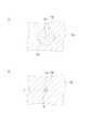
図1乃至図5を参照しつつ、第1実施形態のケーブル接続基板について説明する。図1は第1実施形態のケーブル接続基板の概略構成を模式的に示す説明図である。図2は第1実施形態の基板の概略構成を模式的に示す説明図である。図3(A)は第1層の主要部を示す説明図であり、図3(B)は信号層の主要部を示す説明図であり、図3(C)は第2層の主要部を示す説明図である。図4(A)は基板の第1面側に設けられた第1開口部の周囲を示す説明図であり、図4(B)は基板の第2面側に設けられた第2開口部の周囲を示す説明図である。図5はケーブルの先端部を示す説明図である。なお、図1や図2は、断面図であり、各部材にハッチンが施されている。一方、図3(A)〜図4(B)は断面図ではないが、説明を分かり易くするために、図3(A)〜図4(B)に表わされた各部材には、部材毎に図1や図2に表わされている部材と共通のハッチングが施されている。(First embodiment)
The cable connection substrate of the first embodiment will be described with reference to FIGS. 1 to 5. FIG. 1 is an explanatory diagram schematically showing a schematic configuration of the cable connection board of the first embodiment. FIG. 2 is an explanatory diagram schematically showing the schematic configuration of the substrate of the first embodiment. 3A is an explanatory view showing the main part of the first layer, FIG. 3B is an explanatory view showing the main part of the signal layer, and FIG. 3C is a main part of the second layer. It is an explanatory view shown. FIG. 4A is an explanatory view showing the periphery of the first opening provided on the first surface side of the substrate, and FIG. 4B is the illustration of the second opening provided on the second surface side of the substrate. It is an explanatory view showing the circumference. FIG. 5 is an explanatory view showing the tip of the cable. 1 and 2 are cross-sectional views, and each member is hatched. On the other hand, although FIGS. 3(A) to 4(B) are not cross-sectional views, in order to make the description easy to understand, the members shown in FIGS. 3(A) to 4(B) are The hatching common to the members shown in FIGS. 1 and 2 is given for each.
図1を参照すると、ケーブル接続基板1は、基板10と、この基板10に接続されているケーブル20を備える。本実施形態のケーブル接続基板1は、基板10にケーブル20がコネクタレスで接続されている。図2を参照すると、基板10は、第1面10aと、この第1面10aの裏面側となる第2面10bを備えている。また、基板10には、その内部に少なくとも信号層13と、この信号層13を挟む状態で第1層11及び第2層12とが配置されている。第1層11は、基板10において、信号層13と第1面10aとの間に配置されている。第2層12は、基板10において、信号層13と第2面10bとの間に配置されている。 Referring to FIG. 1, the cable connection board 1 includes a
図3(A)を参照すると、第1層11は、開口部11aを備えている。図3(B)を参照すると、信号層13は、帯状部分の端部に円形状部を備え、さらに、その円形状部の中心部分に接続孔13aを備えている。接続孔13aの周囲は、後に詳述するようにランド13bとなる。図3(C)を参照すると、第2層12は、開口部12aを備えている。 Referring to FIG. 3A, the
本実施形態における第1層11は、基板グランド層であり、第2層12は、基板電源層となっている。ただし、これらの層は、これらの機能に限定されるものではなく、他の機能を有する層であってもよい。例えば、第1層11と第2層12の双方が、基板グランド層であってもよい。 In the present embodiment, the
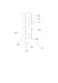
図2を参照すると、基板10の第1面10aには、第1開口部10a1が設けられている。このように、最表面層のレジスト開口を行うことで、ランド11bが露出した状態となっている。ランド11bは、開口部11aの周囲に形成されている。基板10には、第1開口部10a1の中心部に挿通孔10cが設けられている。図4(A)を参照すると、第1開口部10a1の内側にランド11bが露出しており、ランド11bの内側に挿通孔10cが設けられた状態となっている。挿通孔の内周壁面は、信号層13が有する接続孔13aの内周壁面と面一となっている。このような挿通孔10cには、後に詳説するように、ケーブル20の内部導体21が挿入される。これにより、内部導体21が信号層13まで到達できる。 Referring to FIG. 2, the first opening 10a1 is provided on the
図2を参照すると、基板10の第2面10bには、第2開口部10dが設けられている。第2開口部10dは、第2面10b側から信号層13に到達している空間を形成している。第2開口部10dの直径は、第1開口部10a1よりも小さい。第2開口部10dは、第2面10b側からルータ加工を施すことによって穿設されている。図4(B)を参照すると、第2開口部10dは、信号層13まで到達することで、ケーブル20が接続されていない状態の基板10において、ランド13bを第2開口部10d内に露出させている。 Referring to FIG. 2, the
図5を参照すると、ケーブル20は、同軸ケーブルである。ケーブル20は、中心部に内部導体21を備え、その周囲に絶縁体22を備える。そして、絶縁体22の周囲に外部導体23を備える。このようなケーブル20は、基板10の第1面10a側から基板10の内部に向かって挿し込まれる。そして、外部導体23と第1層11とを接合する第1半田接合部31と、基板10内において、内部導体21の先端部と信号層13とを接合する第2半田接合部32とによって、ケーブル20が基板10に接合される。これにより、ケーブル20は、コネクタレスで基板10に接続され、基板10の第1面10a側に延びた状態となる。 Referring to FIG. 5, the
ここで、第1半田接合部31について、説明する。第1半田接合部31は、ランド11bにおいて、第1層11と外部導体23とを半田により接合する。図5を参照すると、外部導体23は、外周壁面23aと先端面23bとを有する。そして、図1を参照すると、外部導体23の先端面23bがランド11bに密着させられている。外部導体23の先端面23bが密着させられているランド11bには、半田が盛られ、第1半田接合部31が形成されている。第1半田接合部31は、ランド11bと外部導体23の外周壁面23aとに密着している。このように外部導体23を第1層11に直接接合することで、外部導体23と第1層11との接合箇所におけるインピーダンスの不整合を解消することができる。また、第1半田接合部31は、ケーブル20の周囲を固定することになるので、ケーブル20の実装強度を向上させることができる。 Here, the 1st solder
つぎに、第2半田接合部32について、説明する。第2半田接合部32は、基板10内において、内部導体21の先端部と信号層13とを接合する。図5を参照すると、内部導体21は、外周壁面21aと先端面21bとを有する。ここで、図1を参照すると、内部導体21の絶縁体22から露出した部分の長さは、内部導体21を接続孔13aに挿し込んだ状態において、先端面21bが信号層13空間側の面を形成するランド13b(信号層13の空間内に位置する面)と面一となるように調整されている。これは、スタブが形成されないようにするための配慮である。第2半田接合部32は、ランド13bと先端面21bを覆うように設けられている。内部導体21は、その外周壁面21aが接続孔13aの内周面と接触すること、及び、第2半田接合部32を介することで、信号層13との導通している。このように内部導体21を信号層13に直接接合することで、内部導体21と信号層13との接合箇所におけるインピーダンスの不整合を解消することができる。 Next, the second solder
このように、本実施形態のケーブル接続基板1によれば、ケーブル20を直接第1層11及び信号層13に接合しているため、ケーブル側と基板側の特性インピーダンスを一致させることが可能となる。すなわち、一般的なコネクタを用いたケーブルと基板との接続と比較して、インピーダンス不整合の一因となるコネクタ接点とケーブルとの接点を排除することができる。また、コネクタを装備する場合、基板の裏面側に、コンタクト半田付け部が形成される。このように基板の表面から突出して形成されるコンタクト半田付け部もインピーダンス不整合の一因となるが、本実施形態では、このようなコンタクト半田付け部も排除することができる。この際、ケーブル20の内部導体21、外部導体23、第1層11及び信号層13の材質を適宜選択することで、より効果的にインピーダンスの不整合を解消することができる。このように、ケーブル20の基板10への接続部におけるインピーダンスの不整合が解消されると、高速伝送に有利となる。 As described above, according to the cable connection board 1 of the present embodiment, since the
さらに、本実施形態のケーブル接続基板1によれば、コネクタを用いない構造であり、コネクタ実装領域が不要となるため、高密度実装に対応しやすくなる。また、本実施形態のケーブル接続基板1は、ケーブル20を直接基板10に接続しているため、隣接信号系統との漏話(クロストーク)が抑制される。また、本実施形態のケーブル接続基板1によれば、内部導体21が基板10内で信号層13と接合しているので、外来ノイズに対する遮蔽性が高く、放射ノイズ(EMI:Electro-Magnetic Interference)による電磁妨害の抑制ともなる。 Further, according to the cable connection board 1 of the present embodiment, since the structure does not use a connector and a connector mounting area is unnecessary, it is easy to support high-density mounting. Further, in the cable connection board 1 of the present embodiment, the
(第2実施形態)
つぎに、図6を参照しつつ、第2実施形態について説明する。第2実施形態のケーブル接続基板50が第1実施形態のケーブル接続基板1と異なる点は、ケーブル接続基板50が誘電体35を備えている点である。第2実施形態の他の構成は、第1実施形態と異なるところがないので、共通する構成要素については、図面中、同一の参照番号を付し、その詳細な説明は省略する。(Second embodiment)
Next, a second embodiment will be described with reference to FIG. The
誘電体35は、基板10の第2面10b側に第2開口部10dとして形成された空間内に配置されている第2半田接合部32を封止している。このように、誘電体35によって第2半田接合部32を封止することで、第2半田接合部32、ひいては、信号層13と内部導体21との接合部と大気との接触を回避することができる。この結果、ノイズの低減を図ることができる。 The dielectric 35 seals the second solder
なお、本実施形態の誘電体35は、第2面10bと面一となるように第2開口部10dを埋めているが、誘電体35により第2半田接合部32を封止できていれば、必ずしも、第2面10bと面一になっていなくてもよい。 Although the dielectric 35 of the present embodiment fills the
第2実施形態のケーブル接続基板50によれば、第1実施形態のケーブル接続基板1と同様の効果を発揮することができると共に、第2半田接合部32が封止されたことによるノイズの低減を図ることができる。 According to the
以上本発明の好ましい実施形態について詳述したが、本発明は係る特定の実施形態に限定されるものではなく、特許請求の範囲に記載された本発明の要旨の範囲内において、種々の変形、変更が可能である。 Although the preferred embodiments of the present invention have been described in detail above, the present invention is not limited to the specific embodiments, and various modifications within the scope of the gist of the present invention described in the claims. It can be changed.
1、50 ケーブル接続基板
10 基板
10a 第1面
10a1 第1開口部
10b 第2面
10c 挿通孔
10d 第2開口部
11 第1層
11b ランド
12 第2層
13 信号層
13a 接続孔
20 ケーブル
21 内部導体
22 絶縁体
23 外部導体
31 第1半田接合部
32 第2半田接合部
35 誘電体1, 50
Claims (3)
Translated fromJapanese外部導体と内部導体とを備えた同軸ケーブルであって、前記基板に接続され、前記基板の第1面側に延びるケーブルと、
前記ケーブルが備える前記外部導体と前記第1層とを接合する第1半田接合部と、
前記基板内において、前記ケーブルが備える前記内部導体の先端部と前記信号層とを接合する第2半田接合部と、
を、備え、
前記第1層は、前記信号層と前記第1面との間に配置されるとともに、前記基板の前記第1面側に形成された開口部内に露出したランドを備え、
前記信号層は、前記内部導体が接続される接続孔を備え、
前記第1半田接合部は、前記外部導体の先端面を前記第1層が備える前記ランドに密着させた状態で前記外部導体と前記第1層とを接合しており、
前記第2半田接合部は、外周壁面を前記接続孔の内周面に接触させた状態で前記接続孔に挿し込まれている前記内部導体と前記信号層とを接合している
ケーブル接続基板。A signal layer disposed in the substrate, and a first layer and a second layer disposed in the substrate with the signal layer interposed therebetween,
A coaxial cable including an outer conductor and an inner conductor, the cable being connected to the substrate and extending to the first surface side of the substrate,
A first solder joints joining the first layer andthe outer conductor said cable comprises,
In the substrate, a second solder joint that joins a front end portion ofthe inner conductor the cable and a said signal layer,
Is equipped with
The first layer is disposed between the signal layer and the first surface, andincludes a land exposed in an opening formed on the first surface side of the substrate,
The signal layer includes a connection hole to which the inner conductor is connected,
The first solder joint section joins the outer conductor and the first layer in a state where the tip end surface of the outer conductor is in close contact with the land provided in the first layer,
The second solder joint portion joins the signal conductor with the internal conductor inserted into the connection hole with the outer peripheral wall surface in contact with the inner peripheral surface of the connection hole. Cable connection board.
前記第2半田接合部は、前記空間内に配置されており、
前記空間内に配置され、前記第2半田接合部を封止する誘電体を備える請求項1に記載のケーブル接続基板。The substrate has a space reaching the signal layer from a second surface side which is a back surface side of the first surface,
The second solder joint portion is arranged in the space,
The cable connection board according to claim 1, further comprising a dielectric material that is disposed in the space and seals the second solder joint portion.
前記内部導体の先端面は、前記信号層の前記空間側の面と面一とされている請求項1または2に記載のケーブル接続基板。The substrate has a space reaching the signal layer from a second surface side which is a back surface side of the first surface,
The cable connection board according to claim 1 or 2, wherein a front end surface of the inner conductor is flush with a surface of the signal layer on the space side.
Priority Applications (2)
| Application Number | Priority Date | Filing Date | Title |
|---|---|---|---|
| JP2016087330AJP6711108B2 (en) | 2016-04-25 | 2016-04-25 | Cable connection board |
| US15/486,378US10111319B2 (en) | 2016-04-25 | 2017-04-13 | Cable connection board |
Applications Claiming Priority (1)
| Application Number | Priority Date | Filing Date | Title |
|---|---|---|---|
| JP2016087330AJP6711108B2 (en) | 2016-04-25 | 2016-04-25 | Cable connection board |
Publications (2)
| Publication Number | Publication Date |
|---|---|
| JP2017199726A JP2017199726A (en) | 2017-11-02 |
| JP6711108B2true JP6711108B2 (en) | 2020-06-17 |
Family
ID=60090561
Family Applications (1)
| Application Number | Title | Priority Date | Filing Date |
|---|---|---|---|
| JP2016087330AExpired - Fee RelatedJP6711108B2 (en) | 2016-04-25 | 2016-04-25 | Cable connection board |
Country Status (2)
| Country | Link |
|---|---|
| US (1) | US10111319B2 (en) |
| JP (1) | JP6711108B2 (en) |
Families Citing this family (2)
| Publication number | Priority date | Publication date | Assignee | Title |
|---|---|---|---|---|
| US10490915B2 (en) | 2017-06-07 | 2019-11-26 | Mitas Electronics, Llc | Gaussian chamber cable direct connector |
| CN113395819A (en)* | 2020-03-13 | 2021-09-14 | 华为技术有限公司 | Cable assembly, signal transmission structure and electronic equipment |
Family Cites Families (9)
| Publication number | Priority date | Publication date | Assignee | Title |
|---|---|---|---|---|
| US4701491A (en) | 1986-10-27 | 1987-10-20 | Dow Corning Corporation | Silicone extrusion stock |
| US5046966A (en)* | 1990-10-05 | 1991-09-10 | International Business Machines Corporation | Coaxial cable connector assembly |
| US5199879A (en)* | 1992-02-24 | 1993-04-06 | International Business Machines Corporation | Electrical assembly with flexible circuit |
| JPH0621613A (en)* | 1992-07-01 | 1994-01-28 | Hitachi Constr Mach Co Ltd | Structure of wiring board and coaxial cable connection |
| JPH0637412A (en)* | 1992-07-15 | 1994-02-10 | Fujitsu Ltd | Printed wiring board |
| JPH0766516A (en)* | 1993-08-31 | 1995-03-10 | Ibiden Co Ltd | Printed-wiring board and through hole making method in the same |
| US6541711B1 (en)* | 2000-05-22 | 2003-04-01 | Cisco Technology, Inc. | Isolated ground circuit board apparatus |
| JP2006222386A (en)* | 2005-02-14 | 2006-08-24 | Toshiba Corp | Printed wiring boards, printed circuit boards, electronic equipment |
| JP5506737B2 (en) | 2011-05-27 | 2014-05-28 | 株式会社日立製作所 | Signal transmission circuit |
- 2016
- 2016-04-25JPJP2016087330Apatent/JP6711108B2/ennot_activeExpired - Fee Related
- 2017
- 2017-04-13USUS15/486,378patent/US10111319B2/ennot_activeExpired - Fee Related
Also Published As
| Publication number | Publication date |
|---|---|
| US10111319B2 (en) | 2018-10-23 |
| US20170311435A1 (en) | 2017-10-26 |
| JP2017199726A (en) | 2017-11-02 |
Similar Documents
| Publication | Publication Date | Title |
|---|---|---|
| JP6658263B2 (en) | Board and cable connection board | |
| CN209417411U (en) | Endoscope device and its cable assembly | |
| JP6853655B2 (en) | Connection structure between board and connector and board | |
| JP6430160B2 (en) | Optical module and optical module manufacturing method | |
| WO2011076138A1 (en) | Connector, circuit board with connector, and connecting construction for circuit board | |
| CN103579871B (en) | Radio frequency connector | |
| CN111312663A (en) | pipe socket | |
| TWI806146B (en) | High speed transmission cable and cable end connector with high speed transmission cable | |
| JP6711108B2 (en) | Cable connection board | |
| TW202037014A (en) | Electrical connector and connector device | |
| US7145083B2 (en) | Reducing or eliminating cross-talk at device-substrate interface | |
| TWI446664B (en) | Cable connector assembly | |
| TWI806435B (en) | Connector cable | |
| JP6060759B2 (en) | Differential signal transmission cable connection structure and cable connector assembly | |
| TWI689949B (en) | Circuit board assembly with high-speed wire | |
| CN101093923A (en) | connector structure | |
| US20220077556A1 (en) | Transmission line and electronic device | |
| JP2015159372A (en) | Transmission line structure, housing, and electronic apparatus | |
| JP2014002852A (en) | Structure of connection between differential pair transmission cable and connector | |
| CN206412558U (en) | Micro-coaxial wire cable assembly and the web camera with the micro-coaxial wire cable assembly | |
| CN110418497A (en) | PCB board splicing structure and antenna device | |
| CN206574874U (en) | Electric connector and the mating electrical connector coordinated with it | |
| TWI606658B (en) | Cable connector, carrier module thereof, and method for assembling the same | |
| TWI885471B (en) | Electrical connector cable assembly | |
| JP3229385U (en) | Flexible flat cable structure |
Legal Events
| Date | Code | Title | Description |
|---|---|---|---|
| A621 | Written request for application examination | Free format text:JAPANESE INTERMEDIATE CODE: A621 Effective date:20190115 | |
| A131 | Notification of reasons for refusal | Free format text:JAPANESE INTERMEDIATE CODE: A131 Effective date:20190924 | |
| A977 | Report on retrieval | Free format text:JAPANESE INTERMEDIATE CODE: A971007 Effective date:20190919 | |
| A521 | Request for written amendment filed | Free format text:JAPANESE INTERMEDIATE CODE: A523 Effective date:20191121 | |
| A131 | Notification of reasons for refusal | Free format text:JAPANESE INTERMEDIATE CODE: A131 Effective date:20200107 | |
| A521 | Request for written amendment filed | Free format text:JAPANESE INTERMEDIATE CODE: A523 Effective date:20200303 | |
| TRDD | Decision of grant or rejection written | ||
| A01 | Written decision to grant a patent or to grant a registration (utility model) | Free format text:JAPANESE INTERMEDIATE CODE: A01 Effective date:20200428 | |
| A61 | First payment of annual fees (during grant procedure) | Free format text:JAPANESE INTERMEDIATE CODE: A61 Effective date:20200511 | |
| R150 | Certificate of patent or registration of utility model | Ref document number:6711108 Country of ref document:JP Free format text:JAPANESE INTERMEDIATE CODE: R150 | |
| LAPS | Cancellation because of no payment of annual fees |