JP6706805B2 - Semiconductor laser device - Google Patents
Semiconductor laser deviceDownload PDFInfo
- Publication number
- JP6706805B2 JP6706805B2JP2017523099AJP2017523099AJP6706805B2JP 6706805 B2JP6706805 B2JP 6706805B2JP 2017523099 AJP2017523099 AJP 2017523099AJP 2017523099 AJP2017523099 AJP 2017523099AJP 6706805 B2JP6706805 B2JP 6706805B2
- Authority
- JP
- Japan
- Prior art keywords
- layer
- strain
- refractive index
- composition
- cladding
- Prior art date
- Legal status (The legal status is an assumption and is not a legal conclusion. Google has not performed a legal analysis and makes no representation as to the accuracy of the status listed.)
- Active
Links
Images


Classifications
- H—ELECTRICITY
- H01—ELECTRIC ELEMENTS
- H01S—DEVICES USING THE PROCESS OF LIGHT AMPLIFICATION BY STIMULATED EMISSION OF RADIATION [LASER] TO AMPLIFY OR GENERATE LIGHT; DEVICES USING STIMULATED EMISSION OF ELECTROMAGNETIC RADIATION IN WAVE RANGES OTHER THAN OPTICAL
- H01S5/00—Semiconductor lasers
- H01S5/20—Structure or shape of the semiconductor body to guide the optical wave ; Confining structures perpendicular to the optical axis, e.g. index or gain guiding, stripe geometry, broad area lasers, gain tailoring, transverse or lateral reflectors, special cladding structures, MQW barrier reflection layers
- H01S5/22—Structure or shape of the semiconductor body to guide the optical wave ; Confining structures perpendicular to the optical axis, e.g. index or gain guiding, stripe geometry, broad area lasers, gain tailoring, transverse or lateral reflectors, special cladding structures, MQW barrier reflection layers having a ridge or stripe structure
- H01S5/2205—Structure or shape of the semiconductor body to guide the optical wave ; Confining structures perpendicular to the optical axis, e.g. index or gain guiding, stripe geometry, broad area lasers, gain tailoring, transverse or lateral reflectors, special cladding structures, MQW barrier reflection layers having a ridge or stripe structure comprising special burying or current confinement layers
- H01S5/2206—Structure or shape of the semiconductor body to guide the optical wave ; Confining structures perpendicular to the optical axis, e.g. index or gain guiding, stripe geometry, broad area lasers, gain tailoring, transverse or lateral reflectors, special cladding structures, MQW barrier reflection layers having a ridge or stripe structure comprising special burying or current confinement layers based on III-V materials
- H—ELECTRICITY
- H01—ELECTRIC ELEMENTS
- H01S—DEVICES USING THE PROCESS OF LIGHT AMPLIFICATION BY STIMULATED EMISSION OF RADIATION [LASER] TO AMPLIFY OR GENERATE LIGHT; DEVICES USING STIMULATED EMISSION OF ELECTROMAGNETIC RADIATION IN WAVE RANGES OTHER THAN OPTICAL
- H01S5/00—Semiconductor lasers
- H01S5/20—Structure or shape of the semiconductor body to guide the optical wave ; Confining structures perpendicular to the optical axis, e.g. index or gain guiding, stripe geometry, broad area lasers, gain tailoring, transverse or lateral reflectors, special cladding structures, MQW barrier reflection layers
- H01S5/22—Structure or shape of the semiconductor body to guide the optical wave ; Confining structures perpendicular to the optical axis, e.g. index or gain guiding, stripe geometry, broad area lasers, gain tailoring, transverse or lateral reflectors, special cladding structures, MQW barrier reflection layers having a ridge or stripe structure
- H—ELECTRICITY
- H01—ELECTRIC ELEMENTS
- H01S—DEVICES USING THE PROCESS OF LIGHT AMPLIFICATION BY STIMULATED EMISSION OF RADIATION [LASER] TO AMPLIFY OR GENERATE LIGHT; DEVICES USING STIMULATED EMISSION OF ELECTROMAGNETIC RADIATION IN WAVE RANGES OTHER THAN OPTICAL
- H01S5/00—Semiconductor lasers
- H01S5/30—Structure or shape of the active region; Materials used for the active region
- H01S5/32—Structure or shape of the active region; Materials used for the active region comprising PN junctions, e.g. hetero- or double- heterostructures
- H01S5/3201—Structure or shape of the active region; Materials used for the active region comprising PN junctions, e.g. hetero- or double- heterostructures incorporating bulkstrain effects, e.g. strain compensation, strain related to polarisation
- H—ELECTRICITY
- H01—ELECTRIC ELEMENTS
- H01S—DEVICES USING THE PROCESS OF LIGHT AMPLIFICATION BY STIMULATED EMISSION OF RADIATION [LASER] TO AMPLIFY OR GENERATE LIGHT; DEVICES USING STIMULATED EMISSION OF ELECTROMAGNETIC RADIATION IN WAVE RANGES OTHER THAN OPTICAL
- H01S5/00—Semiconductor lasers
- H01S5/30—Structure or shape of the active region; Materials used for the active region
- H01S5/32—Structure or shape of the active region; Materials used for the active region comprising PN junctions, e.g. hetero- or double- heterostructures
- H01S5/3211—Structure or shape of the active region; Materials used for the active region comprising PN junctions, e.g. hetero- or double- heterostructures characterised by special cladding layers, e.g. details on band-discontinuities
- G—PHYSICS
- G03—PHOTOGRAPHY; CINEMATOGRAPHY; ANALOGOUS TECHNIQUES USING WAVES OTHER THAN OPTICAL WAVES; ELECTROGRAPHY; HOLOGRAPHY
- G03B—APPARATUS OR ARRANGEMENTS FOR TAKING PHOTOGRAPHS OR FOR PROJECTING OR VIEWING THEM; APPARATUS OR ARRANGEMENTS EMPLOYING ANALOGOUS TECHNIQUES USING WAVES OTHER THAN OPTICAL WAVES; ACCESSORIES THEREFOR
- G03B21/00—Projectors or projection-type viewers; Accessories therefor
- G03B21/14—Details
- G03B21/20—Lamp housings
- G03B21/2006—Lamp housings characterised by the light source
- G03B21/2033—LED or laser light sources
- H—ELECTRICITY
- H01—ELECTRIC ELEMENTS
- H01S—DEVICES USING THE PROCESS OF LIGHT AMPLIFICATION BY STIMULATED EMISSION OF RADIATION [LASER] TO AMPLIFY OR GENERATE LIGHT; DEVICES USING STIMULATED EMISSION OF ELECTROMAGNETIC RADIATION IN WAVE RANGES OTHER THAN OPTICAL
- H01S2301/00—Functional characteristics
- H01S2301/17—Semiconductor lasers comprising special layers
- H01S2301/173—The laser chip comprising special buffer layers, e.g. dislocation prevention or reduction
- H—ELECTRICITY
- H01—ELECTRIC ELEMENTS
- H01S—DEVICES USING THE PROCESS OF LIGHT AMPLIFICATION BY STIMULATED EMISSION OF RADIATION [LASER] TO AMPLIFY OR GENERATE LIGHT; DEVICES USING STIMULATED EMISSION OF ELECTROMAGNETIC RADIATION IN WAVE RANGES OTHER THAN OPTICAL
- H01S5/00—Semiconductor lasers
- H01S5/20—Structure or shape of the semiconductor body to guide the optical wave ; Confining structures perpendicular to the optical axis, e.g. index or gain guiding, stripe geometry, broad area lasers, gain tailoring, transverse or lateral reflectors, special cladding structures, MQW barrier reflection layers
- H01S5/2004—Confining in the direction perpendicular to the layer structure
- H01S5/2009—Confining in the direction perpendicular to the layer structure by using electron barrier layers
- H—ELECTRICITY
- H01—ELECTRIC ELEMENTS
- H01S—DEVICES USING THE PROCESS OF LIGHT AMPLIFICATION BY STIMULATED EMISSION OF RADIATION [LASER] TO AMPLIFY OR GENERATE LIGHT; DEVICES USING STIMULATED EMISSION OF ELECTROMAGNETIC RADIATION IN WAVE RANGES OTHER THAN OPTICAL
- H01S5/00—Semiconductor lasers
- H01S5/30—Structure or shape of the active region; Materials used for the active region
- H01S5/305—Structure or shape of the active region; Materials used for the active region characterised by the doping materials used in the laser structure
- H01S5/3054—Structure or shape of the active region; Materials used for the active region characterised by the doping materials used in the laser structure p-doping
- H01S5/3063—Structure or shape of the active region; Materials used for the active region characterised by the doping materials used in the laser structure p-doping using Mg
- H—ELECTRICITY
- H01—ELECTRIC ELEMENTS
- H01S—DEVICES USING THE PROCESS OF LIGHT AMPLIFICATION BY STIMULATED EMISSION OF RADIATION [LASER] TO AMPLIFY OR GENERATE LIGHT; DEVICES USING STIMULATED EMISSION OF ELECTROMAGNETIC RADIATION IN WAVE RANGES OTHER THAN OPTICAL
- H01S5/00—Semiconductor lasers
- H01S5/30—Structure or shape of the active region; Materials used for the active region
- H01S5/34—Structure or shape of the active region; Materials used for the active region comprising quantum well or superlattice structures, e.g. single quantum well [SQW] lasers, multiple quantum well [MQW] lasers or graded index separate confinement heterostructure [GRINSCH] lasers
- H01S5/3403—Structure or shape of the active region; Materials used for the active region comprising quantum well or superlattice structures, e.g. single quantum well [SQW] lasers, multiple quantum well [MQW] lasers or graded index separate confinement heterostructure [GRINSCH] lasers having a strained layer structure in which the strain performs a special function, e.g. general strain effects, strain versus polarisation
- H01S5/3406—Structure or shape of the active region; Materials used for the active region comprising quantum well or superlattice structures, e.g. single quantum well [SQW] lasers, multiple quantum well [MQW] lasers or graded index separate confinement heterostructure [GRINSCH] lasers having a strained layer structure in which the strain performs a special function, e.g. general strain effects, strain versus polarisation including strain compensation
- H—ELECTRICITY
- H01—ELECTRIC ELEMENTS
- H01S—DEVICES USING THE PROCESS OF LIGHT AMPLIFICATION BY STIMULATED EMISSION OF RADIATION [LASER] TO AMPLIFY OR GENERATE LIGHT; DEVICES USING STIMULATED EMISSION OF ELECTROMAGNETIC RADIATION IN WAVE RANGES OTHER THAN OPTICAL
- H01S5/00—Semiconductor lasers
- H01S5/30—Structure or shape of the active region; Materials used for the active region
- H01S5/34—Structure or shape of the active region; Materials used for the active region comprising quantum well or superlattice structures, e.g. single quantum well [SQW] lasers, multiple quantum well [MQW] lasers or graded index separate confinement heterostructure [GRINSCH] lasers
- H01S5/343—Structure or shape of the active region; Materials used for the active region comprising quantum well or superlattice structures, e.g. single quantum well [SQW] lasers, multiple quantum well [MQW] lasers or graded index separate confinement heterostructure [GRINSCH] lasers in AIIIBV compounds, e.g. AlGaAs-laser, InP-based laser
- H01S5/34333—Structure or shape of the active region; Materials used for the active region comprising quantum well or superlattice structures, e.g. single quantum well [SQW] lasers, multiple quantum well [MQW] lasers or graded index separate confinement heterostructure [GRINSCH] lasers in AIIIBV compounds, e.g. AlGaAs-laser, InP-based laser with a well layer based on Ga(In)N or Ga(In)P, e.g. blue laser
Landscapes
- Physics & Mathematics (AREA)
- Condensed Matter Physics & Semiconductors (AREA)
- General Physics & Mathematics (AREA)
- Electromagnetism (AREA)
- Optics & Photonics (AREA)
- Geometry (AREA)
- Semiconductor Lasers (AREA)
- Led Devices (AREA)
Description
Translated fromJapanese本開示は、高出力の光源に関し、特に窒化物半導体よりなる発光素子に関する。 The present disclosure relates to a high-output light source, and more particularly to a light emitting device made of a nitride semiconductor.
従来、大画面の画像を効率的に得るための一形態として、映像信号に応じた画像を形成する小型の液晶パネル等の空間光変調素子を、ランプなどの光源からの光で照明し、投射レンズによってその光学像をスクリーン上に拡大投射する投射型画像表示装置としてプロジェクタが広く用いられている。このようなプロジェクタなどの投射型画像表示装置においては、可視光の波長帯域で高い発光効率が得られる超高圧水銀ランプで光源を構成することが一般的である。 Conventionally, as one mode for efficiently obtaining an image on a large screen, a spatial light modulator such as a small liquid crystal panel that forms an image according to a video signal is illuminated with light from a light source such as a lamp and projected. BACKGROUND ART A projector is widely used as a projection type image display device for enlarging and projecting an optical image on a screen by a lens. In such a projection-type image display device such as a projector, it is common to configure the light source with an ultra-high pressure mercury lamp that can obtain high luminous efficiency in the wavelength band of visible light.
これに対して、昨今、プロジェクタの光源に高圧水銀ランプではなく、半導体素子であるLED(Light Emitting Diode)が用いられている。LEDプロジェクタは消費電力が低く、静音性が高く、ランプ寿命が長いといった特徴があり、本体サイズも小型になる。 On the other hand, in recent years, an LED (Light Emitting Diode), which is a semiconductor element, is used as a light source of a projector instead of a high pressure mercury lamp. The LED projector has features such as low power consumption, high noise reduction, and long lamp life, and the main body size becomes small.
しかしながら、LEDは発光層である活性層における自然放出光を利用しているために輝度が十分とはいえない。このため、光源にワット級(すなわち1W以上)の大出力が可能な半導体レーザにより蛍光体を励起し、可視域の光に対して十分な輝度を得ることが可能なレーザプロジェクタが注目されている。 However, the LED does not have sufficient brightness because it utilizes the spontaneous emission light from the active layer, which is the light emitting layer. For this reason, a laser projector that can excite a phosphor with a semiconductor laser capable of a large output of watt class (that is, 1 W or more) as a light source and obtain sufficient brightness for light in the visible region is drawing attention. ..
一般式がIn1−x−yGaxAlyN(0≦x≦1、0≦y≦1)で表される窒化物系材料を用いた半導体レーザ(窒化物系半導体レーザ)は、可視光から紫外光まで発光可能であり、上記レーザプロジェクタの光源として好適である。General formulaIn 1-x-y Ga x Al y N (0 ≦ x ≦ 1,0 ≦ y ≦ 1) semiconductor laser using a nitride-based material expressed with (nitride semiconductor laser) visible It can emit light from light to ultraviolet light, and is suitable as a light source for the laser projector.
例えば、窒化物系半導体レーザで青色、緑色光の光源を形成し、AlGaInP系材料を用いたレーザを赤色光源とすれば、小型低消費電力のレーザプロジェクタを実現することができる。 For example, when a blue light source and a green light source are formed with a nitride semiconductor laser and a laser using an AlGaInP material is used as a red light source, a compact and low power consumption laser projector can be realized.
ここで、プロジェクタ光源に使用される半導体レーザには、ワット級の大出力動作のみならず、50℃以上の高温動作時においても10000時間以上の長期動作が要望されている。 Here, the semiconductor laser used for the projector light source is required to have a long-term operation of 10,000 hours or more even at a high temperature operation of 50° C. or more, as well as a large output operation of a watt class.
これに対し、例えば、図11に示す特許文献1にかかる従来の発明において発振波長430nm帯の窒化物系青色レーザに関する技術(第1の従来技術)が開示されている。 On the other hand, for example, in the conventional invention according to
この従来の発明においては、GaN基板101上に、Al0.05Ga0.95Nバッファ層102、n型コンタクト層103、クラック防止層104、n型クラッド層105、n型光ガイド層106、n側第1窒化物半導体層131b、多重量子井戸活性層107、p型電子閉じ込め層108、p側第1窒化物半導体層131a、p型光ガイド層109、p型クラッド層110、およびp型コンタクト層111よりなる積層構造にリッジストライプを形成することにより発振波長448nmにおいてレーザ発振を得ている。n型コンタクト層103は、SiドープAl0.05Ga0.95Nからなる。クラック防止層104は、In0.06Ga0.94Nからなり厚さ0.15μmである。n型クラッド層105は、厚さ2.5nmのアンドープAl0.05Ga0.95Nと厚さ2.5nmのSiドープGaNとからなる組み合わせを200回繰り返した超格子である。n型光ガイド層106は、アンドープのGaNからなり、厚さ0.1μmである。n側第1窒化物半導体層131bは、厚さ50nmのSiドープのIn0.05Ga0.95Nからなる。多重量子井戸活性層107は、厚さ13nmのアンドープのIn0.05Ga0.95Nの障壁層が3層とアンドープのIn0.32Ga0.68Nよりなる厚さ2.5nmの井戸層が2層とからなる。p型電子閉じ込め層108は、厚さ10nmのMgドープAl0.3Ga0.7N層からなる。p側第1窒化物半導体層131aは、厚さ50nmのMgドープIn0.05Ga0.95N層からなる。p型光ガイド層109は、厚さ0.15μmのアンドープのGaNからなる。p型クラッド層110は、厚さ2.5nmのアンドープAl0.05Ga0.95Nと厚さ2.5nmのMgドープGaNとからなる組み合わせを90回繰り返した厚さ0.45μmの超格子である。p型コンタクト層111は、厚さ15nmのMgドープのp型GaN層からなる。In this conventional invention, Al0.05 Ga0.95 N
図11に示す従来構造においては、n型クラッド層105とp型クラッド層110により、多重量子井戸活性層への垂直方向(本願において、基板の法線方向を垂直方向と呼ぶ。また、レーザ共振器端面に平行で基板の法線方向に垂直な方向を水平方向と呼ぶ。)の光閉じ込めを行い、p型クラッド層110に形成したリッジにより水平方向の光閉じ込めを行い、レーザ発振を可能としている。 In the conventional structure shown in FIG. 11, the n-
また、従来の発明においては、p型電子閉じ込め層108とp型クラッド層110との間に備えた、厚さ50nmのMgドープIn0.05Ga0.95N層よりなる第1窒化物半導体層131aと厚さ0.15μmのアンドープのGaNよりなるp型光ガイド層109とにより、光分布の活性層への垂直方向の光閉じ込め率を増大している。Further, in the conventional invention, the first nitride semiconductor formed of the Mg-doped In0.05 Ga0.95 N layer having a thickness of 50 nm provided between the p-type
また、p型電子閉じ込め層108により、活性層に注入した電子がp型クラッド層へ漏れるキャリアオーバーフローを低減している。 Further, the p-type
この構造において、量子井戸活性層に厚さ2.5nm、In組成0.32のInGaNウェル層を2層用いることで、温度特性の向上とレーザ発振しきい電流値の低減を図った波長448nmの青色レーザを実現している。 In this structure, by using two InGaN well layers having a thickness of 2.5 nm and an In composition of 0.32 for the quantum well active layer, a wavelength of 448 nm for improving temperature characteristics and reducing the laser oscillation threshold current value is obtained. Realizes a blue laser.
なお、以下3元混晶であるAlxGa1−xN(0<x<1)をAlGaN、InyGa1−yN(0<y<1)をInGaN、4元混晶であるInyAlxGa1−x−yN(0<x<1、0<y<1)をInAlGaNと表記することがある。In the following, Alx Ga1-x N (0<x<1) which is a ternary mixed crystal is AlGaN, Iny Ga1-y N (0<y<1) is InGaN, and quaternary mixed crystal Iny Al x Ga 1-x- y N a (0 <x <1,0 <y <1) is sometimes referred to as InAlGaN.
プロジェクタ光源に使用される半導体レーザ素子には、ワット級の大出力動作のみならず、50℃以上の高温動作時においても10000時間以上の長期動作が要望されている。従って、波長445nm帯の青色域、及び、波長530nm帯の緑色域において、高温、高出力動作可能な半導体レーザを実現する必要がある。 A semiconductor laser device used for a projector light source is required to have a long-term operation of 10,000 hours or more even at a high temperature operation of 50° C. or more, as well as a large output operation of a watt class. Therefore, it is necessary to realize a semiconductor laser capable of operating at high temperature and high output in the blue region of the wavelength band of 445 nm and the green region of the wavelength band of 530 nm.
ここで、発振波長が405nmの青紫色域から530nmの青色域へと長波長化するに伴い、活性層に広く用いられるInGaN層と、クラッド層に広く用いられるAlGaN層との屈折率差が小さくなる。このため、クラッド層にAlGaN材料を用いた窒化物系レーザにおいては、波長405nm帯の青紫色レーザに対して長波長の発振波長445nm帯の青色レーザ、さらに長波長の発振波長530nm帯の緑色レーザのように、波長が長い発振波長域の窒化物レーザは、垂直方向の光閉じ込めが小さくなるという課題がある。 Here, as the oscillation wavelength becomes longer from the blue-violet region of 405 nm to the blue region of 530 nm, the difference in refractive index between the InGaN layer widely used for the active layer and the AlGaN layer widely used for the cladding layer becomes small. Become. Therefore, in the nitride-based laser using the AlGaN material for the clad layer, a blue laser having a long wavelength of 445 nm and a green laser having a long wavelength of 530 nm are used for a blue-violet laser having a wavelength of 405 nm. As described above, the nitride laser in the oscillation wavelength region having a long wavelength has a problem that the optical confinement in the vertical direction becomes small.
この課題を解決するためには、クラッド層に用いるAlGaN層のAl組成を0.1以上に高くすれば良いが、この場合、AlGaN層と活性層に用いるInGaN層の熱膨張係数の差が大きくなり、クラックや格子欠陥が発生してしまう。 In order to solve this problem, the Al composition of the AlGaN layer used for the cladding layer may be increased to 0.1 or more. In this case, the difference in thermal expansion coefficient between the AlGaN layer and the InGaN layer used for the active layer is large. And cracks and lattice defects will occur.
本開示は、上記課題を解決するためになされたものであり、波長445nm帯のレーザにおいて、クラックの発生を抑制するためにInGaNバッファ層を用いた構造において、ΔNの低下、光閉じ込め係数の低下を抑制可能なレーザを実現することを目的とする。 The present disclosure has been made in order to solve the above problems, and in a laser having a wavelength of 445 nm, in a structure using an InGaN buffer layer to suppress generation of cracks, a decrease in ΔN and a decrease in optical confinement coefficient. The objective is to realize a laser that can suppress
上記課題を解決するために、本開示の発光素子は、GaN基板と、GaN基板上に形成された、第1導電型のInxGa1−xN(0.01≦x≦0.03)よりなる第1歪補正層と、第1歪補正層の上に形成された、第1導電型のIn1−a−bGaaAlbNからなり、かつ(a/0.98)+(b/0.8)≧1、(a/1.02)+(b/0.85)≦1、(a/1.03)+(b/0.68)≧1の関係を有する第1低屈折率層と、第1低屈折率層の上に形成された、第1導電型のAlzGa1−zN(0.03≦z≦0.06)からなり、かつ第1低屈折率層よりも屈折率の高い第1クラッド層と、第1クラッド層の上に形成された活性層と、を備えている。In order to solve the above problems, a light emitting device according to the present disclosure includes a GaN substrate and a first conductivity type Inx Ga1-x N (0.01≦x≦0.03) formed on the GaN substrate. And a first strain correction layer formed of In1-a-b Gaa Alb N formed on the first strain correction layer, and (a/0.98)+( b/0.8)≧1, (a/1.02)+(b/0.85)≦1, and (a/1.03)+(b/0.68)≧1 A low refractive index layer and a first conductivity type Alz Ga1-z N (0.03≦z≦0.06) formed on the first low refractive index layer and having a first low refractive index The first clad layer has a higher refractive index than the refractive index layer, and an active layer formed on the first clad layer.
上記構成において、(a/0.98)+(b/0.8)≧1、(a/1.02)+(b/0.85)≦1、(a/1.03)+(b/0.68)≧1の関係を有することにより、第1導電型のIn1−a−bGaaAlbNからなる第1低屈折率層は、Al組成が0.06のAlGaNよりも屈折率が低く、かつ、GaNとの格子定数の差を、Al組成が0.1のAlGaNとGaNとの間の格子定数の差よりも小さくすることができる。さらに第1導電型のAlzGa1−zNからなる第1クラッド層のAl組成zの範囲を、0.03≦z≦0.06とすることで、第1低屈折率層の屈折率は、第1クラッド層の屈折率よりも低くすることが可能となる。その結果、垂直方向の光分布が、屈折率の低い第1低屈折率層で減衰するため、屈折率の高い第1歪補正層の影響を受けにくくなり、ΔNの低下を抑制することができる。また、第1低屈折率層により、垂直方向の光分布のGaN基板方向への拡がりが抑制されるため、光閉じ込め係数が小さくなるのを防止することができる。In the above structure, (a/0.98)+(b/0.8)≧1, (a/1.02)+(b/0.85)≦1, (a/1.03)+(b /0.68)≧1 so that the first low-refractive-index layer made of thefirst- conductivity-type In1-a-b Gaa Alb N is better than AlGaN having an Al composition of 0.06. The difference in the lattice constant from GaN, which has a low refractive index, can be made smaller than the difference in the lattice constant between AlGaN and GaN having an Al composition of 0.1. Further, by setting the range of the Al composition z of the first clad layer made of the first conductivity type Alz Ga1-z N to 0.03≦z≦0.06, the refractive index of the first low refractive index layer is set. Can be lower than the refractive index of the first cladding layer. As a result, the light distribution in the vertical direction is attenuated in the first low-refractive index layer having a low refractive index, so that it is less affected by the first distortion correction layer having a high refractive index, and the decrease in ΔN can be suppressed. .. Further, since the first low refractive index layer suppresses the spread of the vertical light distribution in the GaN substrate direction, it is possible to prevent the light confinement coefficient from decreasing.
本開示の発光素子は、さらに、活性層の上に形成され、第2導電型の AltGa1−tN(0≦t≦1)からなり、かつGaN基板より活性層へ向う方向に凸となるリッジ部を有する第2クラッド層と、を備えることが好ましい。The light emitting device of the present disclosure is further formed on the active layer, is made of a second conductivity type Alt Ga1-t N (0≦t≦1), and is convex in a direction from the GaN substrate toward the active layer. And a second cladding layer having a ridge portion that becomes
本開示の発光素子は、さらに、第1歪補正層のIn組成xの範囲を、0.01≦x≦0.03とすることが好ましい。この好ましい構成によれば、圧縮性の歪がかかる第1歪補正層の上に結晶成長した第1クラッド層、第2クラッド層で生じる引っ張り性の歪を補償できるため、GaN基板上に形成したダブルへテロ構造の全体の平均的な歪の大きさが低減し、クラックの発生を抑制することができる。 In the light emitting device of the present disclosure, it is preferable that the In composition x of the first strain correction layer has a range of 0.01≦x≦0.03. According to this preferable configuration, the tensile strain generated in the first clad layer and the second clad layer, which are crystal-grown on the first strain correction layer to which compressive strain is applied, can be compensated, so that the strain is formed on the GaN substrate. The average magnitude of strain in the entire double hetero structure is reduced, and the occurrence of cracks can be suppressed.
この結果、クラックの発生を抑制しつつ、ΔNの低下、光閉じ込め係数の低下を抑制することができる。 As a result, it is possible to suppress the occurrence of cracks and the decrease of ΔN and the light confinement coefficient.
本開示の発光素子は、さらに、第1歪補正層の層厚が0.1μm以上かつ0.2μm以下であることが好ましい。この好ましい構成によれば、第1歪補正層で格子欠陥が生じるのを抑制でき、第1クラッド層および第2クラッド層で生じる引っ張り性の応力を補償でき、クラックの発生を抑制することができる。 In the light emitting device of the present disclosure, it is preferable that the layer thickness of the first strain correction layer is 0.1 μm or more and 0.2 μm or less. According to this preferable configuration, it is possible to suppress the occurrence of lattice defects in the first strain correction layer, compensate for the tensile stress generated in the first cladding layer and the second cladding layer, and suppress the occurrence of cracks. ..
本開示の発光素子は、さらに、第1低屈折率層は、第1導電型のAlbGa1−bN (0.06≦b≦0.1)より形成されていることが好ましい。In the light emitting device of the present disclosure, it is preferable that the first low refractive index layer is further formed of a first conductivity type Alb Ga1-b N (0.06≦b≦0.1).
本開示の発光素子は、さらに、第1低屈折率層の層厚は10nm以上かつ100nm以下であることが好ましい。この好ましい構成によれば、第1低屈折率層の層厚を10nm以上かつ100nm以下とすることにより、発光素子の動作電圧の増大を防止でき、ΔNの低下と光閉じ込め係数の低下とを抑制することができる。 In the light emitting device of the present disclosure, the layer thickness of the first low refractive index layer is preferably 10 nm or more and 100 nm or less. According to this preferable configuration, by increasing the layer thickness of the first low-refractive index layer to 10 nm or more and 100 nm or less, it is possible to prevent an increase in the operating voltage of the light emitting element, and suppress a decrease in ΔN and a light confinement coefficient. can do.
本開示の発光素子の好ましい構成は、さらに、第1低屈折率層が、平均原子組成がIn1−a−bGaaAlbNの単一量子井戸構造または多重量子井戸である。A preferable configuration of the light emitting device of the present disclosure is that the first low refractive index layer further has a single quantum well structure or a multiple quantum well structure having an average atomic composition of In1-a-b Gaa Alb N.
この好ましい構成とすることで、多重量子井戸低屈折率層を構成する各層の層厚を臨界層厚以下とすることで、第1低屈折率層での格子欠陥の発生を抑制することが可能となる。この結果、素子の長期動作における信頼性が向上する。 With this preferable configuration, it is possible to suppress the occurrence of lattice defects in the first low-refractive-index layer by making the layer thickness of each layer forming the multiple quantum well low-refractive-index layer below the critical layer thickness. Becomes As a result, the reliability of the device in long-term operation is improved.
本開示の発光素子は、さらに、第1クラッド層において、z≦0.04であることが好ましい。 In the light emitting device of the present disclosure, z≦0.04 is preferable in the first cladding layer.
本開示の発光素子は、さらに、第1クラッド層において、層厚が1μm以下であり、かつ0.03≦z≦0.04であることが好ましい。の好ましい構成によれば、層全体の平均歪を圧縮性の歪とすることが可能となる。この場合、活性層に注入されたキャリアのオーバーフローが抑制されるため、発光素子の高温動作特性が向上し、動作電流値が小さくなる。そのため、発光素子の長期動作に関する信頼性が向上する。 In the light emitting device of the present disclosure, it is preferable that the first cladding layer has a layer thickness of 1 μm or less and 0.03≦z≦0.04. According to the preferable configuration of, the average strain of the entire layer can be made the compressive strain. In this case, overflow of the carriers injected into the active layer is suppressed, so that the high temperature operation characteristics of the light emitting element are improved and the operation current value is reduced. Therefore, the reliability of the light emitting element for long-term operation is improved.
本開示の発光素子は、さらに、GaN基板と、第1歪補正層との間には、GaN基板より第1導電型のAlsGa1−sN(0<s≦0.01)よりなる第2歪補正層を備えていることが好ましい。この好ましい構成とすること、すなわちAlsGa1−sNよりなる第2歪補正層のAl組成を0.01以下とすることにより、第2歪補正層の臨界層厚を300nm以上とすることができ、GaN基板との格子不整合による格子欠陥の発生を抑制することが可能となる。The light emitting device of the present disclosure further includes, between the GaN substrate and the first strain correction layer, Als Ga1-s N (0<s≦0.01) of a first conductivity type than the GaN substrate. It is preferable to include a second distortion correction layer. With this preferable configuration, that is, by setting the Al composition of the second strain correction layer made of Als Ga1 -s N to 0.01 or less, the critical layer thickness of the second strain correction layer is set to 300 nm or more. Therefore, it is possible to suppress the occurrence of lattice defects due to lattice mismatch with the GaN substrate.
本開示の発光素子は、さらに、第2歪補正層と第1歪補正層との間に第1導電型のGaNよりなる中間層が順次形成されたことが好ましい。この好ましい構成によれば、第2歪補正層の上にGaNよりなる中間層を備えることにより結晶性を回復させることができる。そしてその上に第1歪補正層を形成することで、第1歪補正層を形成しても、引っ張り性の歪が生じる第2歪補正層と、圧縮性の歪が生じる第1歪補正層とで、歪を補償することができるため、中間層と第1歪補正層との界面での格子欠陥の発生を抑制することが可能となる。この結果、素子の長期動作信頼性の劣化を防止することが可能となる。 In the light emitting device of the present disclosure, it is preferable that an intermediate layer made of GaN of the first conductivity type is sequentially formed between the second strain correction layer and the first strain correction layer. According to this preferable configuration, the crystallinity can be restored by providing the intermediate layer made of GaN on the second strain correction layer. Then, by forming the first strain correction layer on the first strain correction layer, even if the first strain correction layer is formed, the second strain correction layer that produces tensile strain and the first strain correction layer that produces compressive strain Since the strain can be compensated by, the occurrence of lattice defects at the interface between the intermediate layer and the first strain correction layer can be suppressed. As a result, it is possible to prevent deterioration of long-term operation reliability of the device.
本開示の発光素子は、さらに、活性層と、第2クラッド層との間に、第2導電型のAlhGa1−hN(0<h≦1)よりなる電子障壁層を備えることが好ましい。The light emitting device of the present disclosure may further include an electron barrier layer made of a second conductivity type Alh Ga1-h N (0<h≦1) between the active layer and the second cladding layer. preferable.
本開示の発光素子は、さらに、電子障壁層は、圧縮歪を有することが好ましい。 Further, in the light emitting device of the present disclosure, the electron barrier layer preferably has compressive strain.
本開示の発光素子は、さらに、第2クラッド層は、圧縮歪を有することが好ましい。 Further, in the light emitting device of the present disclosure, it is preferable that the second cladding layer has compressive strain.
本開示の発光素子は、さらに、活性層は、InfGa1−fN(0<f≦1)よりなるウェル層と、AlgGa1−gN(0≦g≦1)よりなるバリア層とを少なくとも1層含む量子井戸であることが好ましい。Light-emitting device of the present disclosure further, the activelayer, Inf Ga 1-f N and (0 <f ≦ 1) from become welllayer, Al g Ga 1-g N (0 ≦ g ≦ 1) from consisting barrier And a quantum well including at least one layer.
本開示の発光素子は、さらに、活性層は、ウェル層を少なくとも2層含む、多重量子井戸であることが好ましい。 In the light emitting device of the present disclosure, it is preferable that the active layer is a multiple quantum well including at least two well layers.
本開示の発光素子は、さらに、活性層は、2重量子井戸または3重量子井戸であることが好ましい。 Further, in the light emitting device of the present disclosure, the active layer is preferably a double quantum well or a triple quantum well.
本開示の発光素子は、さらに、活性層の特性波長は445nm以上であることが好ましい。 In the light emitting device of the present disclosure, the characteristic wavelength of the active layer is preferably 445 nm or more.
本開示の発光素子により、波長445nm帯以上の長波長のレーザにおいて、クラックの発生を抑制するためにInGaNバッファ層を用いた構造において、ΔNの低下、光閉じ込め係数の低下を抑制できる。 With the light emitting device of the present disclosure, it is possible to suppress a decrease in ΔN and a decrease in optical confinement coefficient in a structure using an InGaN buffer layer for suppressing generation of cracks in a laser having a long wavelength of 445 nm band or longer.
この結果、長期信頼性動作に優れ、高温動作時において温度特性に優れた発光波長445nm帯以上の長波長帯のワット級の窒化物系ワット級レーザを実現できる。 As a result, it is possible to realize a watt-class nitride-based watt-class laser having a long-wavelength band of an emission wavelength of 445 nm or more, which has excellent long-term reliability and excellent temperature characteristics during high-temperature operation.
(本発明の基礎となった知見)
本発明者らは、背景技術の欄において記載した発光素子に関し、以下の問題が生じることを見出した。(Findings that form the basis of the present invention)
The present inventors have found that the following problems occur in the light emitting device described in the background art section.
プロジェクタ光源に使用される半導体レーザ素子には、ワット級の大出力動作のみならず、50℃以上の高温動作時においても10000時間以上の長期動作が要望されている。従って、波長445nm帯の青色域及び、波長530nm帯の緑色域において、高温、高出力動作可能な半導体レーザを実現する必要がある。 A semiconductor laser device used for a projector light source is required to have a long-term operation of 10,000 hours or more even at a high temperature operation of 50° C. or more, as well as a large output operation of a watt class. Therefore, it is necessary to realize a semiconductor laser capable of operating at high temperature and high output in the blue region of the wavelength of 445 nm and the green region of the wavelength of 530 nm.
ここで、発振波長が405nmの青紫色域から530nmの青色域へと長波長化するに伴い、活性層に広く用いられるInGaN層と、クラッド層に広く用いられるAlGaN層との屈折率差が小さくなる。このため、クラッド層にAlGaN材料を用いた窒化物系レーザにおいては、波長405nm帯の青紫色レーザに対して長波長の発振波長445nm帯の青色レーザ、さらに長波長の発振波長530nm帯の緑色レーザのように、波長が長い発振波長域の窒化物レーザは、垂直方向の光閉じ込めが小さくなるという課題がある。 Here, as the oscillation wavelength becomes longer from the blue-violet region of 405 nm to the blue region of 530 nm, the difference in refractive index between the InGaN layer widely used for the active layer and the AlGaN layer widely used for the cladding layer becomes small. Become. Therefore, in the nitride-based laser using the AlGaN material for the clad layer, a blue laser having a long wavelength of 445 nm and a green laser having a long wavelength of 530 nm are used for a blue-violet laser having a wavelength of 405 nm. As described above, the nitride laser in the oscillation wavelength region having a long wavelength has a problem that the optical confinement in the vertical direction becomes small.
この課題を解決するためには、クラッド層に用いるAlGaN層のAl組成を0.1以上に高くすれば良いが、この場合、AlGaN層と活性層に用いるInGaN層の熱膨張係数の差が大きくなり、クラックや格子欠陥が発生してしまう。さらに、p型AlGaNクラッド層が高抵抗化し、素子の動作電圧が増大してしまう。このため、クラックの発生を抑制するためには、クラッド層にAlGaN層を用いる場合、Al組成は0.1程度以上に高めることは困難である。また、Al組成が0.05から0.1の間のAlGaN層をクラッド層に用いたとしても、p型AlGaN層の抵抗が高くなりやすく、動作電圧の増大を招いてしまう。動作電圧が増大すると素子がレーザ発振した場合における素子の自己発熱が増大し、温度特性が劣化してしまう。 In order to solve this problem, the Al composition of the AlGaN layer used for the cladding layer may be increased to 0.1 or more. In this case, the difference in thermal expansion coefficient between the AlGaN layer and the InGaN layer used for the active layer is large. And cracks and lattice defects will occur. Furthermore, the p-type AlGaN cladding layer has a high resistance, and the operating voltage of the device increases. Therefore, in order to suppress the occurrence of cracks, it is difficult to increase the Al composition to about 0.1 or more when using an AlGaN layer for the cladding layer. Further, even if an AlGaN layer having an Al composition of 0.05 to 0.1 is used for the cladding layer, the resistance of the p-type AlGaN layer is likely to be high, which causes an increase in operating voltage. When the operating voltage increases, the self-heating of the device increases when the device oscillates, and the temperature characteristics deteriorate.
また、波長405nm帯の青紫色レーザに対して、所望の発振波長を得るためには量子井戸活性層におけるInGaNウェル層のIn組成は0.07程度であったが、発振波長445nm帯の青色レーザにおいてはInGaNウェル層のIn組成は0.15程度以上が必要となる。さらに、発振波長530nm帯の緑色レーザにおいてはInGaNウェル層のIn組成が0.3程度以上である高In組成のInGaN層が必要となる。InGaN層において、In組成が高くなると、GaN基板との格子不整合が大きくなるのみならず、InGaN層を構成するInNとGaNの安定なIII族−V族原子間距離が異なるために結晶内部に蓄積される内部歪エネルギーが大きくなる。この内部歪エネルギーを低減するために、高In組成のInGaN層においてはIn組成の高い領域と低い領域に組成が分離する組成分離が生じやすくなる。InGaN層を成長する温度である800℃付近の温度では、In組成が0.15付近以上の高In組成となると熱力学的に不安定となり、組成分離が生じやすくなる。組成分離が生じると、ウェル層内でバンドギャップエネルギーの面内分布にバラツキが生じ、バンドギャップ波長の小さい部分はIn組成が高く格子欠陥が生じやすいのみならず、レーザ発振光に対し、光吸収中心となり、発振しきい電流値や電流−光出力特性における外部微分効率(以下、スロープ効率)の低下を招くことになる。この結果、動作電流値が大きくなり、温度特性の劣化をもたらすことになり、実用上重大な支障をきたすことになる。 Further, in order to obtain a desired oscillation wavelength with respect to a blue-violet laser having a wavelength of 405 nm, the In composition of the InGaN well layer in the quantum well active layer was about 0.07, but a blue laser having an oscillation wavelength of 445 nm band was used. In, the In composition of the InGaN well layer must be about 0.15 or more. Further, in a green laser having an oscillation wavelength of 530 nm band, an InGaN layer having a high In composition, in which the In composition of the InGaN well layer is about 0.3 or more, is required. When the In composition in the InGaN layer is high, not only the lattice mismatch with the GaN substrate becomes large, but also the stable III-V group interatomic distance between InN and GaN forming the InGaN layer is different from each other. The internal strain energy accumulated increases. In order to reduce this internal strain energy, in the InGaN layer having a high In composition, composition separation in which the composition is separated into a high In composition region and a low In composition region is likely to occur. At a temperature near 800° C. at which the InGaN layer is grown, if the In composition becomes a high In composition of about 0.15 or more, it becomes thermodynamically unstable and composition separation easily occurs. When the composition separation occurs, the in-plane distribution of the bandgap energy varies in the well layer, and the portion having a small bandgap wavelength has a high In composition and is likely to have a lattice defect. At the center, the oscillation threshold current value and the external differential efficiency (hereinafter referred to as slope efficiency) in the current-optical output characteristics are reduced. As a result, the operating current value becomes large and the temperature characteristics are deteriorated, which causes a serious problem in practical use.
そこで、組成分離や格子不整合による格子欠陥の発生を抑制するために、高In組成のウェル層の層厚を3nm以下に薄くしてInGaNウェル層の体積を小さくし、その上に成長する障壁層にはGaNないしは、GaNとの格子不整合が小さいIn組成0.05程度以下のInGaN層を10nm程度以上成長し結晶性の回復を行うことが効果的である。このような構成とすれば、薄いウェル層の上下が、GaN層ないし、GaN層に格子定数が近いInGaNで挟まれる構造となり、InGaN層に格子欠陥が生じる臨界層厚を超えることなく、InGaNウェル層の組成分離をある程度抑制することが可能となる。これは、障壁層とウェル層との界面で発生するウェル層と障壁層間の格子不整合による歪エネルギーにより高In組成層であっても、組成分離を生じない方が熱力学に安定となるためである。この様に、高In組成のInGaNウェル層の層厚は3nm程度以下と薄くする必要がある。 Therefore, in order to suppress the occurrence of lattice defects due to composition separation and lattice mismatch, the layer thickness of the well layer having a high In composition is reduced to 3 nm or less to reduce the volume of the InGaN well layer, and the barrier grown on the well layer is reduced. It is effective to recover the crystallinity by growing GaN or an InGaN layer having an In composition of about 0.05 or less, which has a small lattice mismatch with GaN, by about 10 nm or more. With this structure, the thin well layer has a structure in which the upper and lower sides of the thin well layer are sandwiched between GaN layers or InGaN having a lattice constant close to that of the GaN layer, and the InGaN layer does not exceed the critical layer thickness where lattice defects occur. It is possible to suppress the compositional separation of layers to some extent. This is because thermodynamics is more stable if composition separation does not occur due to strain energy generated at the interface between the barrier layer and the well layer due to lattice mismatch between the well layer and the barrier layer, even if the composition ratio is high. Is. As described above, the InGaN well layer having a high In composition needs to be as thin as about 3 nm or less.
この場合、ウェル層の厚さが薄いため活性層への光の閉じ込め係数がなおさら低下してしまうことになる。従って、光閉じ込め係数を増大させるためには、前述のように、クラッド層に用いるAlGaN層のAl組成を0.1以上に可能な限り高くすれば良いが、この場合、AlGaN層と活性層に用いるInGaN層の格子定数の差が大きくなり、クラックや格子欠陥が発生してしまう。 In this case, since the well layer is thin, the light confinement coefficient in the active layer is further reduced. Therefore, in order to increase the optical confinement coefficient, as described above, the Al composition of the AlGaN layer used for the cladding layer may be set as high as possible to 0.1 or higher. The difference in lattice constant between the InGaN layers used becomes large, and cracks and lattice defects occur.
以上のように、波長445nm帯から530nm帯の窒化物系レーザにおいては、InGaN活性層とAlGaNクラッドの屈折率差を大きくすることが困難であり、さらに、ウェル層の層厚は3nm以下の薄い層厚とする必要があるため、垂直方向の光閉じ込め係数が1%程度と非常に小さい値となってしまう。光閉じ込め係数が小さいと、活性層における動作キャリア密度が大きくなり、高温高出力動作時において、活性層からp型クラッド層へのキャリアのオーバーフローが増大し、温度特性の劣化や電流−光出力特性における光出力の熱飽和レベルの低下を招くことになる。 As described above, it is difficult to increase the difference in refractive index between the InGaN active layer and the AlGaN cladding in the nitride-based laser having a wavelength of 445 nm to 530 nm, and the well layer has a small thickness of 3 nm or less. Since it is necessary to make the layer thickness, the light confinement coefficient in the vertical direction becomes a very small value of about 1%. When the optical confinement coefficient is small, the operating carrier density in the active layer becomes large, and the overflow of carriers from the active layer to the p-type cladding layer increases at the time of high-temperature and high-power operation, resulting in deterioration of temperature characteristics and current-optical output characteristics. In this case, the thermal saturation level of the light output in the above will be reduced.
光の閉じ込め係数を増大させるべくAlGaNクラッド層のAl組成を高くするとクラックや格子欠陥が生じやすく、素子の長期動作信頼性上、重大な支障をきたすことになる。 If the Al composition of the AlGaN cladding layer is increased to increase the light confinement coefficient, cracks and lattice defects are likely to occur, which causes a serious problem in terms of long-term operation reliability of the device.
ここで、本発明では、基板の法線方向を垂直方向、共振器端面の面内において、基板の法線方向と垂直な方向を水平方向と呼ぶことにする。 Here, in the present invention, the normal direction of the substrate is referred to as a vertical direction, and the direction perpendicular to the normal direction of the substrate in the plane of the resonator end face is referred to as a horizontal direction.
クラックの発生を防止するためには、特許文献2に示す従来の構造(第2の従来技術)では、図12に示すように、GaNよりなるフリースタンディングの基板201と、基板上に形成されたn型AlxGa1−xN(0≦x≦0.1)よりなる第1バッファ層202と、第1バッファ層上に形成されたn型InyGa1−yN(0<y≦0.1)よりなる第2バッファ層203と、第2バッファ層上にn側クラッド層204、活性層206、p側クラッド層209を順次備えた構造としている。この構成により、バッファ層の機能を、再成長界面からの転位の発生を抑制する第1バッファ層202と、クラックの発生を抑制する第2バッファ層203とに分けることで、フリースタンディングの基板201上に高品質のAlGaN層を成長させ、電気特性の優れた窒化物半導体素子を得ることができることが開示されている。In order to prevent the occurrence of cracks, in the conventional structure (second prior art) disclosed in
しかしながら、この構造において、第2バッファ層202は屈折率が他の層と比較して相対的に高いため、第2バッファ層202と活性層206間の層厚が薄いと、導波路に閉じ込められる光分布は屈折率の高い第2バッファ層202の影響を受け、第2バッファ層202のある基板側に垂直方向の光分布が偏ってしまう。 However, in this structure, the refractive index of the
このようになると、リッジ内外の実効屈折率差(ΔN)が低下し、光分布の水平方向の閉じ込め機構が弱くなり、電流−光出力特性が非線形となるキンクが生じたり、動作電流値が高くなるという課題が生じる。この場合、垂直方向光分布が第2バッファ層202まで広がらないように、第2バッファ層202と活性層間206のn側クラッド層204の層厚を厚くするか、基板と活性層間のn側クラッド層のAl組成を高くして垂直方向の光閉じ込めを強くすれば良いが、このようにすると、n側クラッド層204での応力が大きくなり、クラックが生じやすくなる。あるいは、p側クラッド層209のAl組成をn側クラッド層204のAl組成よりも低く設定し、p側クラッド層209の屈折率を相対的にn側クラッド層204よりも高くして、垂直方向光分布を相対的にp型層寄りとする方法も考えられるが、活性層206における光閉じ込め係数が小さくなり、温度特性が劣化してしまう。 In this case, the effective refractive index difference (ΔN) inside and outside the ridge is reduced, the horizontal confinement mechanism of the light distribution is weakened, a kink occurs in which the current-light output characteristic becomes non-linear, and the operating current value is high. The problem arises that In this case, the thickness of the n-side clad
このため、InGaNバッファ層を用いた従来の波長445nm帯のレーザにおいては、n側クラッド層の層厚が薄くして、n側クラッド層でのクラックの発生を抑制すると、ΔNの低下、光閉じ込め係数の低下を招き、電流−光出力特性が線形性に優れ、温度特性も優れたレーザを実現することが困難であった。 Therefore, in the conventional laser of wavelength 445 nm band using the InGaN buffer layer, if the layer thickness of the n-side cladding layer is made small to suppress the occurrence of cracks in the n-side cladding layer, the ΔN is reduced and the optical confinement is suppressed. It has been difficult to realize a laser having a good coefficient of current-light output characteristics and excellent temperature characteristics, since the coefficient is lowered.
本開示は、上記課題を解決するためになされたものであり、波長445nm帯のレーザにおいて、クラックの発生を抑制するためにInGaNバッファ層を用いた構造において、ΔNの低下、光閉じ込め係数の低下を抑制可能なレーザを実現することを目的とする。 The present disclosure has been made in order to solve the above problems, and in a laser having a wavelength of 445 nm, in a structure using an InGaN buffer layer to suppress generation of cracks, a decrease in ΔN and a decrease in optical confinement coefficient. The objective is to realize a laser that can suppress
以下、本開示にかかる発明の実施の形態について図面を参照しながら、説明を行う。 Hereinafter, embodiments of the invention according to the present disclosure will be described with reference to the drawings.
(第1の実施形態)
(1−1 素子構造)
本開示の第1の実施形態に係る発光素子の構造に関する断面図を図1に示す。図1に示す発光素子は、主面をc面((0001)面)とするGaN基板11上に、InGaNよりなり層厚が0.1μmであるn型の第1歪補正層12、層厚が0.05μmであるn型のAlGaNよりなる第1低屈折率層13、n型のAlGaNよりなる第1クラッド層14、層厚が0.2μmであるN型のGaNよりなる光ガイド層15、InGaN系材料からなる多重量子井戸の活性層16、層厚が20nmであり、Al組成が0.2であるAlGaNよりなるp型の電子障壁層17、p型のAlGaNよりなる第2クラッド層18、層厚が0.1μmであるp型のGaNよりなるコンタクト層19、発光光に対して透明なSiO2よりなる電流ブロック層20、p側電極22、及び、n側電極21が形成されてなる。この発光素子は、半導体レーザ装置である。第2クラッド層18にはリッジ18aが形成されているが、このリッジ18aの底部の幅(W)は8.0μmである。また、リッジ18aは、GaN基板11より離れるにつれて幅が狭くなっている。なお、p側電極22は、NiとPtとAuとの積層構造よりなり、N側電極21は、TiとAlとの積層構造よりなる。(First embodiment)
(1-1 element structure)
A cross-sectional view of the structure of the light emitting device according to the first embodiment of the present disclosure is shown in FIG. The light emitting device shown in FIG. 1 has an n-type first
第2クラッド層18は、リッジ18aの上部と活性層16までの距離を0.7μmとし、リッジ18aの下端部と活性層16との距離をdp(0.05μm)としている。なお、n型のドーパントとしてはSiが用いられており、n型半導体層には1018cm−3程度のSiが添加されている。また、p型のドーパントとしてはMgが用いられ、p型半導体層には1019cm−3程度のMgが添加されている。In the second clad
なお、電子障壁層17は、活性層16に閉じ込められた電子が第2クラッド層18へあふれる(キャリアオーバーフロー)のを抑制するために設けられる。 The
本開示の第1の実施形態に係る発光素子は、リッジストライプの半導体レーザ装置であり、リッジ18aは図1の紙面に垂直な方向に沿って延び、その長さは1000μmである。また、発光素子の前端面(図示せず)には低反射率(AR)コートがなされ、後端面(図示せず)には高反射率(HR)コートがなされている。前端面及び後端面は、ともにリッジ18aの延びる方向に垂直であり、前端面と後端面との間で共振器を形成している。 The light emitting device according to the first embodiment of the present disclosure is a semiconductor laser device having a ridge stripe, and the
本開示の第1の実施形態に係る発光素子の発光波長は、445nmである。 The emission wavelength of the light emitting device according to the first embodiment of the present disclosure is 445 nm.
(1−2 第1クラッド層14および第2クラッド層18のAl組成の検討)
ここで、第1クラッド層14及び第2クラッド層18のAl組成を大きくすると、活性層16と第1クラッド層14との間の屈折率差、および活性層16と第2クラッド層18との間の屈折率差を大きくすることができ、活性層16に垂直な方向に光を強く閉じ込めることが可能となり、発振しきい電流値を小さくすることが可能となる。しかしながらAlGaNとGaNとの格子定数の差のために、第1クラッド層14および第2クラッド層18のAl組成を大きくしすぎると格子欠陥が生じ信頼性の低下につながる。さらに、Al組成を高めると、p型不純物の活性化率の低下により、第2クラッド層18の抵抗が大きくなり、発光素子の直列抵抗の増大につながる。そのため、第1クラッド層14および第2クラッド層18のAl組成の上限は0.1以下、より好ましくは0.05以下ということになる。(1-2 Investigation of Al composition of first clad
Here, when the Al composition of the first clad
一方、波長445nm帯以上の長波長帯では、活性層16とAlGaN材料との間の屈折率差が小さくなり、垂直方向の光閉じ込め係数が低下する。このため、第1クラッド層14および第2クラッド層18のAl組成を可能な限り高めて、垂直方向の光閉じ込め係数を増大させる必要がある。特に波長445nm帯およびそれよりも長波長の領域では、InGaN層とAlGaN層との屈折率を大きくすることが波長405nm帯よりも難しく、垂直方向光閉じ込め係数を大きくすることが困難である。垂直方向の光閉じ込め係数を大きくするためには、第1クラッド層14および第2クラッド層18のAl組成を0.03以上にしなければならない。 On the other hand, in the long wavelength band of 445 nm or more, the difference in the refractive index between the
従って、第1クラッド層14および第2クラッド層18のAl組成は0.03以上とすることが好ましく、Al組成の上限として0.1以下、より好ましくは0.05以下であることが好ましい。 Therefore, the Al composition of the first clad
(1−3 活性層16のウェル層数の検討)
発光素子の活性層16として、ウェル(井戸)層が単一または複数である量子井戸構造が用いられる。波長が445nmのレーザ発振を得るためには、ウェル層のIn組成を0.15程度とする必要がある。しかしながら、In組成が0.15であるInGaNとGaNと間の格子不整合は約1.6%であり、ウェル層厚を3nmより厚くすると、ウェル層の臨界層厚を大きく上回り格子欠陥が生じてしまう。格子欠陥は、光吸収中心となり、発光素子の発振しきい電流値や動作電流値の増大を招き、信頼性の低下につながるため、極力その発生を抑制する必要がある。従って、ウェル層の厚さは3nm以下とするのが好ましい。(1-3 Examination of the number of well layers of active layer 16)
As the
一方、ウェル層厚が薄いと、発光素子の垂直方向の光閉じ込め係数が低下する。そこで、ウェル層の層厚を多くする必要がある。ところが、ウェル層の層数が4層以上となると、各ウェル層の動作キャリア密度にばらつきが生じやすくなり、各ウェル層の最大利得を与える利得ピーク波長がばらついてしまう。この結果、発振しきい電流値が増大してしまう。また、ウェル層の間にある障壁層の層数も多くなるため、発光素子の直列抵抗の増大や、ピエゾ効果による障壁層の電位ポテンシャルの傾きの影響が増大し、動作電圧が増大してしまう。この結果、ウェル層数を多くしすぎると、発振しきい電流値が大きくなり、かつ動作電圧が高い発光素子となってしまう。この結果、発光素子の温度特性が劣化してしまう。 On the other hand, when the well layer is thin, the light confinement coefficient in the vertical direction of the light emitting element is lowered. Therefore, it is necessary to increase the layer thickness of the well layer. However, when the number of well layers is four or more, the operating carrier density of each well layer tends to vary, and the gain peak wavelength that gives the maximum gain of each well layer also varies. As a result, the oscillation threshold current value increases. Further, since the number of barrier layers between the well layers also increases, the series resistance of the light emitting element increases and the influence of the potential potential gradient of the barrier layers due to the piezo effect increases, and the operating voltage increases. .. As a result, if the number of well layers is too large, the oscillation threshold current value becomes large and the operating voltage becomes high. As a result, the temperature characteristics of the light emitting element deteriorate.
また、ウェル層数が1すなわち単一量子井戸構造では光閉じ込め係数が小さくなり、動作キャリア密度が増大するため、キャリアオーバーフローが増大し、電流―光出力特性において熱飽和する光出力が低下してしまう。従って、ウェル層厚が3nm以下の薄いウェル層であっても、ウェル層数は2層備えた2重量子井戸(Double Quantum Well、DQW)構造、または3層備えた3重量子井戸(Triple Quantum Well、TQW)構造とする必要がある。 Further, in the case where the number of well layers is one, that is, in the single quantum well structure, the optical confinement coefficient becomes small and the operating carrier density increases, so that carrier overflow increases, and the optical output that is thermally saturated in the current-optical output characteristics decreases. I will end up. Therefore, even if the well layer is a thin well layer having a thickness of 3 nm or less, the number of well layers is a double quantum well (DQW) structure having two layers, or a triple quantum well having three layers (triple quantum well). Well, TQW) structure is required.
本開示の第1の実施形態の発光素子における活性層16は、厚さ3nm、In組成0.15のInGaNよりなるウェル層を2層備え、バリア層としてGaNとした2重量子井戸構造としている。 The
(1−4 第1歪補正層12の導入)
波長445nm帯およびそれよりも長波長の領域では、InGaN層とAlGaN層の屈折率を大きくすることが波長405nm帯よりも難しく、垂直方向光閉じ込め係数を大きくすることが困難である。垂直方向の光閉じ込め係数を大きくするためには、第1クラッド層14および第2クラッド層18のAl組成を0.03以上にしなければならない。この場合、第1クラッド層14の層厚が1.5μm程度となると、GaN基板11と第1クラッド層14との間の格子定数の差により、格子欠陥やクラックが発生しやすくなってしまう。(1-4 Introduction of the first distortion correction layer 12)
In the wavelength range of 445 nm and longer wavelengths, it is more difficult to increase the refractive index of the InGaN layer and the AlGaN layer than in the wavelength of 405 nm band, and it is difficult to increase the vertical optical confinement coefficient. In order to increase the optical confinement coefficient in the vertical direction, the Al composition of the
この問題を解決するために、本開示の第1の実施形態にかかる発光素子においては、GaN基板11上にInGaNからなる圧縮性の歪を有する第1歪補正層12を備えている。この結果、第1クラッド層14で生じる引っ張り性の歪を補償できるため、GaN基板11上に結晶成長したエピタキシャル層全体の平均的な歪を小さくすることが可能となり、クラックや格子欠陥の発生を抑制することができる。 In order to solve this problem, the light emitting device according to the first embodiment of the present disclosure includes the first
(1−5 ΔNの検討)
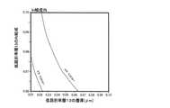
しかしながら、第1歪補正層12の屈折率は、第1クラッド層14の屈折率よりも大きいため、垂直方向の光分布は、図2に示すように、第1歪補正層12によりGaN基板11側へ広がりやすくなる。この結果、リッジ18a内部の光分布及びリッジ外部の光分布の形状が同じ形状となり、リッジ18a内外の実効屈折率差(ΔN)が低下してしまう。ΔNが低下すると、リッジストライプの内外を導波する光分布が、リッジ18aの外側の活性層16で受ける吸収損失の影響が大きくなり、発振しきい値が増大してしまう。さらに、ストライプ内外を導波可能な高次モードの最高次数が小さくなり、導波光のモード数が減るため、各次数のモード間の干渉の影響が大きくなり、電流−光出力特性が非線形性となるキンクが生じやすくなる。この結果、動作電流値が大きくなり、温度特性が低下する。これを防止するためには、3×10⁻³以上の大きさのΔNが必要である。なお、図2において、縦軸は活性層16における光強度を1としたときの光強度(任意単位)の対数を示し、横軸はGaN基板11の表面より少し下側を原点として半導体層の積層方向に沿って測定した各半導体層の位置を表す。図2における番号は、各半導体層の存在位置を示している。図2の縦軸において1E−05は、1×10−5を表す。(1-5 Study of ΔN)
However, since the refractive index of the first
逆に、ΔNを大きくすると、リッジ内部の垂直方向の光分布を第2クラッド層18寄りにする必要がある。この場合、p型の不純物濃度を通常1×1018cm−3以上に大きくしているため、p型不純物によるフリーキャリアの吸収損失の影響を受け、導波路損失が増大し、電流−光出力特性における単位電流あたりの光出力変化(スロープ効率)が低下し、温度特性が低下する。On the contrary, when ΔN is increased, the light distribution in the vertical direction inside the ridge needs to be closer to the
従って、スロープ効率の低下を伴わずに、線形性の良好な電流−光出力特性を得るためには、ΔNを3×10⁻³から6×10⁻³の範囲にする必要がある。Therefore, in order to obtain the current-light output characteristics with good linearity without lowering the slope efficiency, ΔN needs to be in the range of 3×10⁻³ to 6×10⁻³ .
(1−6 第1低屈折率層13のAl組成の検討)
前述のように、第1歪補正層12の影響により、第1クラッド層14の層厚が薄くなるとΔNが低下する。ΔNの低下を抑制するために、本発明の第1の実施の形態にかかる発光素子では、第1クラッド層14よりも屈折率が小さい第1低屈折率層13を備えている。(1-6 Examination of Al composition of first low refractive index layer 13)
As described above, due to the influence of the first
ここで、第1低屈折率層13のΔNに及ぼす影響を見積もるために、第1低屈折率層13に厚さ0.1μmのAlGaNを用いた場合における第1低屈折率層13のAl組成に対するΔNの依存性の計算結果を図3に示す。計算では、第1クラッド層14の層厚を1μm、1.5μm、2μmとし、第1歪補正層12のIn組成を4%としている。 Here, in order to estimate the influence on the ΔN of the first low
図3に示すように、第1クラッド層14の層厚が薄くなるほどΔNの低下が大きいことがわかる。特に、第1クラッド層14の層厚が1μmとなっても、ΔNを3×10⁻³以上とするためには、Al組成0.05以上、つまり、第1クラッド層14のAl組成よりも少なとも0.015以上大きいAl組成を有するAlGaN層を用いる必要があることがわかる。さらに、ΔNを3.5×10⁻³以上とするためには、Al組成が0.06以上、つまり、第1クラッド層14のAl組成よりも少なとも0.025以上大きいAl組成を有するAlGaN層を用いる必要があることがわかる。As shown in FIG. 3, it can be seen that the decrease in ΔN is greater as the layer thickness of the
図4A、図4Bに、第1歪補正層のIn組成をそれぞれ4%、3%とした場合におけるΔNの第1低屈折率層13の組成および層厚依存性の計算結果を示す。図4Bに示すように、第1歪補正層12のIn組成を3%とした場合は、ΔNは、第1低屈折率層13の組成、層厚にあまり依存しないが、第1歪補正層12のIn組成が4%の場合は、ΔNは、第1低屈折率層13の組成、層厚に大きく依存することがわかる。従って、ΔNの第1歪補正層12の影響を受けないようにするためには、第1歪補正層12のIn組成を3%以下とすればよいことがわかる。さらに、第1低屈折率層13のAl組成を0.06から0.1、層厚を10nmから100nmまでの間に設定すれば、4×10⁻³以上のΔNを実現できることがわかる。本発明の第1の実施形態では、第1歪補正層12のIn組成を0.02、第1低屈折率層13の組成を、第1クラッド層14のAl組成より0.025高い0.06、第1クラッド層14の層厚を0.05μmとして、第1クラッド層14の層厚が1μmとなっても、ΔNの防止を抑制可能としている。なお、第1低屈折率層13のAl組成が大きいほど第1低屈折率層13の屈折率を小さくすることができるので活性層16に対する光閉じ込め率を大きくすることができてΔNを大きくすることができるが、反面GaN基板11との格子定数差が大きくなるので第1低屈折率層13の結晶性を悪化させることになる。そのため、第1低屈折率層13のAl組成は、0.1以下であることが好ましい。4A and 4B show the calculation results of the composition and layer thickness dependence of ΔN of the first low
すなわち、第1低屈折率層は、n型のAlbGa1−bN(0.06≦b≦0.1)より形成されていることが好ましい。That is, it is preferable that the first low refractive index layer is formed of n-type Alb Ga1-b N (0.06≦b≦0.1).
また、ΔNの観点から、第1低屈折率層13の層厚は、10nm以上かつ100nm以下であることが好ましい。 From the viewpoint of ΔN, the layer thickness of the first low
以上をまとめると、本開示の第1の実施形態にかかる発光素子の構造パラメータは、表1のようになる。 In summary, the structural parameters of the light emitting device according to the first embodiment of the present disclosure are as shown in Table 1.

なお、活性層16として、ウェル層を層厚が3nmのIn0.15Ga0.85Nとし、バリア層を層厚が3nmのGaNとし、2重量子井戸構造を採用した。As the
第1歪補正層12、第1低屈折率層13、第1クラッド層14および第2クラッド層18のIn組成、Al組成および層厚をパラメータとして検討した。 The In composition, Al composition and layer thickness of the first
(1−7 第1歪補正層12と歪の影響との関係)
次に、第1歪補正層12が、発光素子の各層に及ぼす歪の影響について説明する。(1-7 Relationship between first
Next, the influence of strain exerted on each layer of the light emitting element by the first
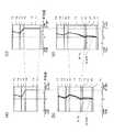
図5および図6に、本開示の第1の実施形態にかかる発光素子の、積層方向に沿った各点の平均歪量の計算結果を比較して示す。なお、図5および図6において、活性層16は積層方向に拡大している。 FIG. 5 and FIG. 6 show comparison results of calculation of the average strain amount at each point along the stacking direction of the light emitting device according to the first embodiment of the present disclosure. 5 and 6, the
なお、検討した第1歪補正層12、第1低屈折率層13、第1クラッド層14および第2クラッド層18のパラメータは、表2、表3のようになる。なお、表2および表3に示す各層を除く層のパラメータは、表1に同じである。 The parameters of the first
本開示の第1の実施形態にかかる発光素子において、第1歪補正層12、第1低屈折率層13が無い場合の構造とし、第1クラッド層14の層厚を1μm、Al組成を0.035とし、第2クラッド層18の層厚を0.7μm、Al組成を0.035とした場合に、第1歪補正層のIn組成を0.01、0.02、0.03とした場合における積層方向の各点の平均歪量の計算結果を図5の(a)に示す。積層方向のある点における平均歪量(Eequ(Z))とは、GaN基板11上に形成された構造における積層方向のある点Zまでの各層の層厚を考慮した歪の平均値のことであり、(式1)で与えられる。 The light emitting device according to the first embodiment of the present disclosure has a structure in which the first
ここで、e(z’)とは、Z方向(積層方向)の点z’における歪のことである。図5の(a)に示すように、第1歪補正層12、第1低屈折率層13が無い場合、第1クラッド層14には均一に8×10⁻⁴程度の引っ張り性の歪がかかり、InGaN系材料の圧縮性の歪のかかる活性層16の領域で平均歪量が補償されて低減し、引っ張り性の歪の生じる第2クラッド層18で再び引っ張り性の歪が増大していることがわかる。この計算結果から、第1歪補正層12、第1低屈折率層13が無い場合、第1クラッド層14に相対的に大きな歪がかかり、第1クラッド層14にクラックや格子欠陥が生じやすいことがわかる。Here, e(z′) is a strain at a point z′ in the Z direction (stacking direction). As shown in FIG. 5A, when the first
本開示にかかる発光素子において、第1歪補正層12の層厚を0.1μmとし、第1低屈折率層13の組成を第1クラッド層のAl組成よりも0.025高い0.06、第1低屈折率層13の層厚を0.05μm、第1クラッド層14の層厚を1μmとし、第2クラッド層18の層厚を0.7μmとした場合に、第1歪補正層12のIn組成を0.01、0.02、0.03とした場合における積層方向の各点の平均歪量の計算結果を図5の(b)に示す。 In the light emitting device according to the present disclosure, the layer thickness of the first
図5の(b)に示すように、第1歪補正層12により、第1クラッド層14に生じる平均歪は、図5の(a)に示す発光素子に対し、第1クラッド層14に生じる平均歪が低減されることがわかる。 As shown in FIG. 5B, the average strain generated in the
これは、第1歪補正層12の圧縮性の歪により、第1クラッド層14の引っ張り性の歪が補償されて低減するためである。この結果、第1歪補正層12のIn組成を0.01から0.03に設定することにより、第1クラッド層14に生じる歪を低減することが可能であることがわかる。 This is because the compressive strain of the first
図5の(c)、図5の(d)はそれぞれ、図5の(a)、図5の(b)の発光素子に対し、第1クラッド層14の層厚を1.5μmとした場合の計算結果を示す。第1クラッド層14の層厚を1.5μmとしても、図5の(b)に示す結果と同様に、第1歪補正層12の圧縮性の歪により、第1クラッド層14の引っ張り性の歪が補償されて低減されることがわかる。 5C and 5D show the case where the thickness of the
図5の(a)から図5の(d)の結果より、第1クラッド層14の層厚が1.0μmから1.5μmまでの範囲で、第1歪補正層12のIn組成を0.01から0.03までの間に設定することにより、第1クラッド層14に生じる歪を低減することが可能であることがわかる。 From the results of (a) to (d) of FIG. 5, the In composition of the first
本開示にかかる発光素子において、第1歪補正層12、第1低屈折率層13が無い場合の構造とし、第1クラッド層14の層厚を1μm、Al組成を0.06とし、第2クラッド層18の層厚を0.7μm、Al組成を0.06とした場合に、第1歪補正層のIn組成を0.01、0.02、0.03とした場合における積層方向の各点の平均歪量の計算結果を図6の(a)に示す。 In the light emitting device according to the present disclosure, a structure without the first
図6の(a)に示すように、第1歪補正層12、第1低屈折率層13が無い場合、第1クラッド層14には均一に1.4×10⁻³程度の歪がかかり、InGaN系材料の圧縮性の歪のかかる活性層16の領域で平均歪量が補償されて低減し、引っ張り性の歪の生じる第2クラッド層18で再び、引っ張り性の歪が増大していることがわかる。この計算結果から、第1歪補正層12、第1低屈折率層13が無い場合、第1クラッド層14に相対的に大きな歪がかかり、第1クラッド層14にクラックや格子欠陥が生じやすいことがわかる。As shown in (a) of FIG. 6, when the first
本開示の第1の実施形態にかかる発光素子において、第1歪補正層12の層厚を0.1μmとし、第1低屈折率層13の組成を第1クラッド層14のAl組成よりも0.025高い0.085、第1低屈折率層13の層厚を0.05μm、第1クラッド層14の層厚を1μmとし、第2クラッド層18の層厚を0.7μmとした場合に、第1歪補正層12のIn組成を0.01、0.02、0.03とした場合における積層方向の各点の平均歪量の計算結果を図6の(b)に示す。 In the light emitting device according to the first embodiment of the present disclosure, the layer thickness of the first
図6の(b)に示すように、第1歪補正層12により、第1クラッド層14に生じる平均歪は、図6の(a)に示す構造に対し、第1クラッド層14に生じる平均歪が低減されることがわかる。 As shown in FIG. 6B, the average strain generated in the
これは、第1歪補正層12の圧縮性の歪により、第1クラッド層14の引っ張り性の歪が補償されて低減するためである。この結果、第1歪補正層12のIn組成を0.01から0.03までの間に設定することにより、第1クラッド層14に生じる歪を低減することが可能であることがわかる。 This is because the compressive strain of the first
図6の(c)、図6の(d)にはそれぞれ、図6の(a)、図6の(b)の構造に対し、第1クラッド層14の層厚を1.5μmとした場合の計算結果を示す。第1クラッド層14の層厚を1.5μmとしても、図6の(b)に示す結果と同様に、第1歪補正層12の圧縮性の歪により、第1クラッド層14の引っ張り性の歪が補償されて低減されることがわかる。 6(c) and 6(d), respectively, in the case where the layer thickness of the
図6の(a)から図6の(d)の結果より、第1クラッド層14の層厚が1.0μmから1.5μmの範囲で、第1歪補正層12のIn組成を0.01から0.03までの間に設定することにより、第1クラッド層14に生じる歪を低減することが可能であることがわかる。 From the results of (a) to (d) of FIG. 6, the In composition of the first
第1歪補正層12の層厚を0.1μmとしているが、この層厚を増加すれば、第1クラッド層14で生じる引っ張り性の歪の補償効果が大きく、第1クラッド層14で生じる引っ張り性の歪の低減効果が大きくなる。 Although the layer thickness of the first
しかしながら、第1歪補正層12をあまりに厚くすると、第1歪補正層12でGaN基板11との格子定数の差で生じる格子欠陥が発生し、結晶性が低下する。実際に、第1歪補正層12の層厚が0.3μmを超えると、第1歪補正層12において格子欠陥が発生しやすくなる。 However, if the first
一方、第1歪補正層の層厚が0.1μmより小さいと第1クラッド層14および第2クラッド層18で生じる引っ張り性の応力を補償する効果が小さくなる。 On the other hand, if the layer thickness of the first strain correction layer is smaller than 0.1 μm, the effect of compensating the tensile stress generated in the
このため、第1歪補正層12で格子欠陥を生じさせずに、第1クラッド層14で生じる引っ張り性の歪の低減効果を得るためには、第1歪補正層12の層厚を0.1μm以上かつ0.3μm以下の間に設定すればよい。 Therefore, in order to obtain the effect of reducing the tensile strain generated in the
(1−8 電子障壁層17および第2クラッド層18にかかる歪の検討)
発光素子が動作するとき、発光素子には熱が発生する。そのとき、活性層16に注入される電子が熱により励起され、電子障壁層17および第2クラッド層18へ電子が流れ出す、いわゆるキャリアオーバーフローという現象が起きやすくなる。(1-8 Investigation of strain applied to
When the light emitting device operates, heat is generated in the light emitting device. At that time, the so-called carrier overflow phenomenon in which the electrons injected into the
ここで、電子障壁層17および第2クラッド層18に圧縮性の歪が付加されると、電子障壁層17および第2クラッド層18のバンドギャップエネルギーが大きくなり、電子障壁層17および第2クラッド層18の電子に対する障壁高さが高くなる。この電子に対する障壁高さが高くなることにより、キャリアオーバーフローを低減することができる。このため、発光素子の高温動作時の発振しきい値や動作電流値が低減し、発光素子の長期動作の信頼性を向上させることができる。 Here, if compressive strain is applied to the
図5の(b)に示すように、第1歪補正層12の層厚が0.1μm、第1クラッド層14の層厚が1μmの場合、第1歪補正層12の効果により、GaN基板11上に形成した層全体の平均歪量は、ほぼ0となっている。このとき、電子障壁層17および第2クラッド層18には圧縮性の歪がかかることになる。すなわち、図5の(b)に示す発光素子においては、キャリアオーバーフローを低減でき、結果として発光素子の長期動作の信頼性を向上させることができる。 As shown in FIG. 5B, when the thickness of the first
なお、第1クラッド層14は層全体に対し引っ張り歪を与えるので、図5の(b)に示す発光素子について第1クラッド層14の層厚を1μm以下とすることにより層全体の平均歪を圧縮性の歪とすることができ、電子障壁層17および第2クラッド層18に圧縮性の歪を付加することができる。 Since the
一方、図6の(b)に示すように、第1クラッド層のAl組成が0.06の場合、層全体の平均歪は引っ張り歪となり、電子障壁層17および第2クラッド層18には引っ張り性の歪が付加されている。この場合は、発光素子のキャリアオーバーフローの低減には好ましくない。従って、層全体の平均歪を圧縮性の歪として電子障壁層17および第2クラッド層18に圧縮性の歪を付加するために、第1クラッド層のAl組成を0.04以下とするのが好ましい。 On the other hand, as shown in FIG. 6B, when the Al composition of the first cladding layer is 0.06, the average strain of the entire layer becomes tensile strain, and the tensile strain is exerted on the
なお、上述のように、垂直方向の光閉じ込め係数を大きくするためには、第1クラッド層14および第2クラッド層18のAl組成を0.03以上にすることが好ましいので、第1クラッド層のAl組成としては、0.03以上かつ0.04以下であることが好ましいのである。 As described above, in order to increase the optical confinement coefficient in the vertical direction, it is preferable that the Al composition of the
(1−9 第1低屈折率層13の材料の検討)
第1低屈折率層13は、AlGaN材料に限らなくとも、Al組成が0.06のAlGaN層よりも小さい屈折率を有するInGaAlNでああってもよい。(1-9 Study on Material of First Low Refractive Index Layer 13)
The first low
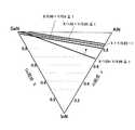
図7にIn1−X−YAlYGaXN(0≦X≦1、0≦Y≦1)に関する組成図を示す。ここでX=a、Y=bとすると、図7においてFIG. 7 shows a composition diagram regarding In1-X-Y AlY GaX N (0≦X≦1, 0≦Y≦1). If X=a and Y=b, then in FIG.
また、
例えば、第1低屈折率層13としてIn0.02Al0.12Ga0.86Nを用いることができる。In0.02Al0.12Ga0.86Nは、(式1)を満たし、かつ(式2)をほぼ満たすので好適である。For example, In0.02 Al0.12 Ga0.86 N can be used as the first low
また、第1低屈折率層13として例えば厚さが5nmのIn0.02Al0.12Ga0.86Nを1層以上、厚さが3nmのIn0.04Al0.24Ga0.72Nを2層以上交互に形成し、単一量子井戸構造または多重量子井戸構造としてもよい。なお、この単一量子井戸構造または多重量子井戸構造を構成する各層の層厚は、上記に限られないことはいうまでもない。As the first low
以上をまとめると、本開示の発光素子は、以下のような構成が好ましいのである。 In summary, the light emitting device of the present disclosure preferably has the following configuration.
すなわち、発光素子として、GaN基板11と、このGaN基板11上に形成された、第1導電型(n型)のInxGa1−xN(0<x≦1)よりなる第1歪補正層12と、この第1歪補正層の上に形成された、第1導電型(n型)のIn1−a−bGaaAlbNからなり、かつ(a/0.98)+(b/0.8)≧1、(a/1.02)+(b/0.85)≦1および(a/1.03)+(b/0.68)≧ 1の関係を有する第1低屈折率層13と、を備えている。そして、この第1低屈折率層13の上に形成された、第1導電型のAlzGa1−zN(0.03≦z≦0.06)からなり、かつ第1低屈折率層よりも屈折率の高い第1クラッド層14と、この第1クラッド層の上に形成された活性層16と、を備えている。That is, as the light emitting element, the
なお、活性層16の上に形成され、第2導電型(p型)の AltGa1−tN(0≦t≦1)からなり、かつGaN基板11より活性層へ向う方向に凸となるリッジ部18aを有する第2クラッド層18を備えていてもよい。In addition, it is formed on the
なお、ここで第1低屈折率層13として、平均の原子組成が上記(式3)〜(式5)を満たすIn1−a−bGaaAlbN層を有する多層構造であってもよく、In1−a−bGaaAlbN層を薄くして量子効果を有する層としてもよい。また、第1低屈折率層として、単一量子井戸構造または2重以上の多重量子井戸構造であってもよい。Here, even if the first low-
(第2の実施形態)
(2−1 素子構造)
本開示の第2の実施形態に係る発光素子は、図8に示すように、図1に示す第1の実施形態に係る発光素子において、GaN基板11と第1歪補正層12との間に、第2歪補正層32および中間層33を備えた構造としている。この構造において、第2歪補正層32はAlGaN材料からなり、Al組成は0.01以下のAl組成を有するAlGaN層としている。また、中間層33はGaN層からなる。この中間層33は、第2歪補正層32上に直接第第1歪補正層12を積層する場合よりも、第1歪補正層12の基板11側での界面で生じる応力を低減することができる。その結果、第2歪補正層32上に直接第1歪補正層12を形成した場合よりも、第1歪補正層12で生じる格子欠陥の発生を抑制することができる。(Second embodiment)
(2-1 Element structure)
As shown in FIG. 8, the light emitting device according to the second embodiment of the present disclosure is the same as the light emitting device according to the first embodiment shown in FIG. 1 between the
第2の実施形態に係る発光素子の、第1歪補正層12からコンタクト層19に至るまでの各半導体層、電流ブロック層20、n側電極21およびp側電極22の構成は、第1の実施形態に係る発光素子と同じである。また、リッジストライプ構造についても第1の実施形態に係る発光素子と同じである。 In the light emitting device according to the second embodiment, each of the semiconductor layers from the first
すなわち、本開示の第2の実施形態に係る発光素子は、第1の実施形態に開示された発光素子に対し、さらに、GaN基板11と、第1歪補正層12との間に、GaN基板11側より第1導電型(n型)のAlsGa1−sN(0<s≦0.01)よりなる第2歪補正層32を備え、さらに第2歪補正層32と第1歪補正層12との間に第1導電型(n型)のGaNよりなる中間層33を有しているのである。That is, the light emitting device according to the second embodiment of the present disclosure is different from the light emitting device disclosed in the first embodiment in that a GaN substrate is provided between the
本開示の第2の実施形態にかかる発光素子の構造パラメータは、表4のようになる。 Table 4 shows the structural parameters of the light emitting device according to the second embodiment of the present disclosure.
図9および図10に、本開示の第2の実施形態にかかる発光素子の、積層方向に沿った各点の平均歪量の計算結果を比較して示す。なお、図9および図10において、活性層16は積層方向に拡大している。なお、検討した第1歪補正層12、第1低屈折率層13、第1クラッド層14および第2クラッド層18のパラメータは、表5、表6のようになる。なお、表5および表6に示す各層を除く層のパラメータは、表4に同じである。 9 and 10 show comparisons of calculation results of the average strain amount at each point along the stacking direction of the light emitting device according to the second embodiment of the present disclosure. In FIGS. 9 and 10, the
また、本開示の第2の実施形態に係る発光素子の発光波長は、445nmである。 The emission wavelength of the light emitting device according to the second embodiment of the present disclosure is 445 nm.
第2歪補正層32、第1低屈折率層13、第1クラッド層14および第2クラッド層18のIN組成、Al組成および層厚をパラメータとして検討した。 The IN composition, Al composition and layer thickness of the second
(2−2 第1歪補正層12と歪の影響との関係)
図9の(a)に、図8に示す本開示の第2の実施形態にかかる発光素子において、第2歪補正層32、中間層33、第1歪補正層12、第1低屈折率層13が無い場合の構造とし、第1クラッド層14の層厚を1μm、Al組成を0.035とし、AlGaN第2クラッド層18の層厚を0.7μm、Al組成を0.035とした場合における積層方向の各点の平均歪量の計算結果を示す。(2-2 Relationship between first
9A, in the light emitting device according to the second embodiment of the present disclosure shown in FIG. 8, the second
図9の(a)に示すように、第2歪補正層32、中間層33、第1歪補正層12、第1低屈折率層13が無い場合、第1クラッド層14には均一に8×10⁻⁴程度の引っ張り性の歪がかかり、InGaN系材料の圧縮性の歪のかかる活性層16の領域で平均歪量が補償されて低減し、引っ張り性の歪の生じる第2クラッド層18で再び引っ張り性の歪が増大していることがわかる。この計算結果から、第1歪補正層12、第1低屈折率層13が無い場合、第1クラッド層14に相対的に大きな歪がかかり、第1クラッド層14にクラックや格子欠陥が生じやすいことがわかる。As shown in FIG. 9A, when the second
図9の(b)に、第2の実施形態にかかる構造において、第2歪補正層32の層厚を1.0μm、Al組成を0.01と0.005、中間層33の層厚を0.1μm、第1歪補正層12の層厚を0.1μmとし、第1低屈折率層13の組成を第1クラッド層14のAl組成よりも0.025高い0.06、第1低屈折率層13の層厚を0.05μm、第1クラッド層14の層厚を1μmとし、AlGaN第2クラッド層18の層厚を0.7μmとした場合に、第1歪補正層12のIn組成を0.02とした場合における積層方向の各点の平均歪量の計算結果を示す。 9B, in the structure according to the second embodiment, the layer thickness of the second
図9(b)に示すように、第2歪補正層32のAl組成が0.005、0.01のいずれの場合においても、第1クラッド層14に生じる平均歪は、図5の(b)に示す発光素子に対し、さらに低減されることがわかる。 As shown in FIG. 9B, when the Al composition of the second
より具体的に述べると、図9の(b)に示す発光素子において層全体の歪は最大でも4×10⁻⁴であり、図5の(b)に示す発光素子と比べて1/5程度の歪量となっている。特に第1歪補正層12および第1低屈折率層13においては歪がほぼ0となっている。このことから、図9の(b)に示す発光素子について、第1歪補正層12および第1低屈折率層13での格子欠陥の発生を抑制することができることがわかる。More specifically, in the light emitting element shown in FIG. 9B, the strain of the entire layer is 4×10⁻⁴ at the maximum, which is about 1/5 of that of the light emitting element shown in FIG. 5B. Is the amount of distortion. In particular, the strain is almost 0 in the first
また、図9の(b)に示す発光素子において、第1クラッド層14の引っ張り性の歪量は図5の(b)に示す発光素子における第1クラッド層14の引っ張り性の歪量よりも小さい。 Further, in the light emitting device shown in FIG. 9B, the tensile strain amount of the
これらは、弱い引っ張り性の歪を有する第2歪補正層32を用いることにより、第1歪補正層12の圧縮性の歪、第1クラッド層14の引っ張り性の歪の平均歪が低減されるためである。 By using the second
このことから、図9の(b)に示す発光素子について、第1歪補正層12、第1低屈折率層13および第1クラッド層14での格子欠陥の発生を抑制できることがわかる。 From this, it is understood that in the light emitting device shown in FIG. 9B, the occurrence of lattice defects in the first
図9の(c)、図9の(d)にはそれぞれ、図9の(a)、図9の(b)の構造に対し、第1クラッド層14の層厚を1.5μmとした場合の計算結果を示す。第1クラッド層14の層厚を1.5μmとしても、図9の(b)に示す結果と同様に、弱い引っ張り性の歪を有する第2歪補正層32を用いることにより、第1歪補正層12の圧縮性の歪、第1クラッド層14の引っ張り性の歪の平均歪が低減されていることがわかる。 9C and 9D show the case where the layer thickness of the
図9の(b)、図9の(d)に示す構造では、第1歪補正層12の層厚を0.1μmとしているが、この層厚が増加すれば、第1クラッド層14で生じる引っ張り性の歪の補償効果が大きくなり、第1クラッド層14で生じる引っ張り性の歪の低減効果が大きくなる。 In the structures shown in (b) of FIG. 9 and (d) of FIG. 9, the layer thickness of the first
しかしながら、第1歪補正層12の層厚をあまりに厚くすると、第1歪補正層12でGaN基板11との格子定数の差で生じる格子欠陥が発生し、結晶性が低下する。このため、第1歪補正層12で格子欠陥を生じさせずに、第1クラッド層14で生じる引っ張り性の歪の低減効果を得るためには、第1歪補正層12の層厚を0.1μmから0.3μmまでの範囲に設定すればよい。 However, if the layer thickness of the first
(2−3 電子障壁層17および第2クラッド層18にかかる歪の検討)
図9の(b)に示すように、第1歪補正層12の層厚が0.1μm、第1クラッド層14の層厚が1μmの場合、第1歪補正層12の効果により、GaN基板11上に形成した層全体の平均歪量は、ほぼ0となっている。このとき、電子障壁層17には圧縮性の歪が付加されることになる。すなわち、図9の(b)に示す発光素子においては、キャリアオーバーフローを低減でき、結果として発光素子の長期動作信頼性を向上させることができる。(2-3 Investigation of strain applied to
As shown in FIG. 9B, when the layer thickness of the first
なお、第1クラッド層14は層全体に対し引っ張り歪を与えるので、図9の(b)に示す発光素子について第1クラッド層14の層厚を1μm以下とすることにより層全体の平均歪を圧縮性の歪とすることができ、電子障壁層17および第2クラッド層18に圧縮性の歪を付加することができる。 Since the first clad
一方、図10の(b)に示すように、第1クラッド層のAl組成が0.06の場合、層全体の平均歪は引っ張り歪となり、電子障壁層17および第2クラッド層18には引っ張り歪が生じている。この場合は、発光素子のキャリアオーバーフローの低減には好ましくない。従って、層全体の平均歪を圧縮性の歪として電子障壁層17および第2クラッド層18に圧縮性の歪を付加するために、第1クラッド層のAl組成を0.04以下とするのが好ましい。 On the other hand, as shown in FIG. 10B, when the Al composition of the first cladding layer is 0.06, the average strain of the entire layer becomes tensile strain, and the
(2−4 第1クラッド層14にかかる歪の検討)
図10の(a)に、図8に示す本開示の第2の実施形態にかかる発光素子において、第2歪補正層32、中間層33、第1歪補正層12、第1低屈折率層13が無い場合の構造とし、第1クラッド層14の層厚を1μm、Al組成を0.06とし第2クラッド層18の層厚を0.7μm、Al組成を0.06とした場合における積層方向の各点の平均歪量の計算結果を示す。(2-4 Examination of strain applied to the first cladding layer 14)
10A, in the light emitting device according to the second embodiment of the present disclosure shown in FIG. 8, the second
図10の(a)に示すように、第2歪補正層32、中間層33、第1歪補正層12、第1低屈折率層13が無い場合、N型第1クラッド層14には均一に1.4×10⁻³程度の引っ張り性の歪がかかり、INGaN系材料の圧縮性の歪のかかる活性層16の領域で平均歪量が補償されて低減し、引っ張り性の歪の生じる第2クラッド層18で再び引っ張り性の歪が増大していることがわかる。この計算結果から、第1歪補正層12、第1低屈折率層13が無い場合、第1クラッド層14に相対的に大きな歪がかかり、第1クラッド層14にクラックや格子欠陥が生じやすいことがわかる。As shown in (a) of FIG. 10, when the second
図10の(b)に、本開示の第2の実施形態にかかる発光素子において、第2歪補正層32の層厚を1.0μm、Al組成を0.01と0.005、中間層33の層厚を0.1μm、第1歪補正層12の層厚を0.1μmとし、第1低屈折率層13の組成を第1クラッド層14のAl組成よりも0.025高い0.085、第1低屈折率層13の層厚を0.05μm、第1クラッド層14の層厚を1μmとし、AlGaN第2クラッド層18の層厚を0.7μmとした場合に、第1歪補正層のIn組成を0.01、0.02、0.03とした場合における積層方向の各点の平均歪量の計算結果を示す。 10B, in the light emitting device according to the second embodiment of the present disclosure, the layer thickness of the second
図10の(b)に示すように、第2歪補正層32のAl組成が0.005、0.01のいずれの場合においても、第1クラッド層14に生じる平均歪は、図6の(b)に示す構造に対し、さらに低減されることがわかる。 As shown in FIG. 10B, when the Al composition of the second
これは、弱い引っ張り性の歪を有する第2歪補正層32を用いることにより、第1歪補正層12の圧縮性の歪、第1クラッド層14の引っ張り性の歪の平均歪が低減されるためである。 By using the second
図10の(c)、図10の(d)にはそれぞれ、図10の(a)、図10の(b)の構造に対し、第1クラッド層14の層厚を1.5μmとした場合の計算結果を示す。第1クラッド層14の層厚を1.5μmとしても、図10の(b)に示す結果と同様に、弱い引っ張り性の歪を有する第2歪補正層32を用いることにより、第1歪補正層12の圧縮性の歪、第1クラッド層14の引っ張り性の歪の平均歪が低減されていることがわかる。 10(c) and 10(d) show the case where the layer thickness of the
図9の(a)から図9の(d)、図10の(a)から図10の(d)の結果より、第1クラッド層と第2クラッド層のAl組成が0.035から0.06の範囲、第1クラッド層14の層厚が1.0μmから1.5μmの範囲で、第2歪補正層32のAl組成を0.005から0.01に設定することにより、第1クラッド層14に生じる歪を低減することが可能であることがわかる。 From the results of FIGS. 9A to 9D and FIGS. 10A to 10D, the Al compositions of the first cladding layer and the second cladding layer are 0.035 to 0. 06, the layer thickness of the
なお、上記第1および第2の実施形態において、活性層16にあるウェル層のIn組成や層厚は上記に限定されず、バリア層の組成や層厚も上記に限定されない。発光素子の発光波長に応じ、活性層16にあるウェル層のIn組成や層厚、バリア層の組成や層厚を適宜選択することができる。 In addition, in the first and second embodiments, the In composition and the layer thickness of the well layer in the
特に、ウェル層のIn組成を0.15より大きくすることにより、発光波長を445nmより大きくすることができ、青色や緑色といった発光を得ることができる。例えば、ウェル層にIn0.3Ga0.7Nを用いれば、発光波長を530nmとすることができる。In particular, by setting the In composition of the well layer to be larger than 0.15, the emission wavelength can be made larger than 445 nm, and blue or green light emission can be obtained. For example, if In0.3 Ga0.7 N is used for the well layer, the emission wavelength can be set to 530 nm.
また、上記第1および第2の実施形態において、第1クラッド層14および第2クラッド層のAl組成を等しくしているが、必ずしもその必要はなく、第1クラッド層14と第2クラッド層のAl組成が異なっていてもよい。 Further, in the first and second embodiments, the Al compositions of the
また、上記第1および第2の実施形態において、発光素子の層構造を、GaN基板11のc面上に形成しているが、c面上に限らず、c面より傾いた面すなわちGaNのオフ基板の上に発光素子の層構造を形成してもよく、m面、r面またはa面を主面とするGaN基板の上に発光素子の層構造を形成してもよい。 Further, in the first and second embodiments, the layer structure of the light emitting element is formed on the c-plane of the
上記第1及び第2の実施形態において、半導体レーザ素子関して議論したが、LED素子に対しても本開示に係る技術は適用可能であり、クラックや格子欠陥の発生が抑制された、青色や青色よりも長波長帯のLED素子を実現することができる。 In the first and second embodiments, the semiconductor laser device was discussed, but the technology according to the present disclosure can be applied to the LED device, and the generation of cracks and lattice defects is suppressed. It is possible to realize an LED element having a wavelength band longer than that of blue.
本開示に係る発明によれば、波長445nm帯以上の発光素子において、1ワット以上の超高出力動作可能な温度特性に優れ、長期信頼性を保証できるワット級の光源を実現する。特に、プロジェクタ光源用に用いられるワット級の光源に利用することができる。なお、プロジェクタ光源用に限らず、例えば車載ヘッドランプ用の光源としても利用することができるし、競技場の照明用光源としても利用することができる。 According to the invention of the present disclosure, a watt-class light source that is excellent in temperature characteristics capable of operating at an ultrahigh output of 1 watt or more and has long-term reliability can be realized in a light emitting element having a wavelength of 445 nm or more. In particular, it can be used for a watt-class light source used for a projector light source. The light source can be used not only as a light source for a projector light source but also as, for example, a light source for an on-vehicle headlamp, or as a light source for illuminating a stadium.
11 GaN基板
12 第1歪補正層
13 第1低屈折率層
14 第1クラッド層
15 光ガイド層
16 活性層
17 電子障壁層
18 第2クラッド層
19 コンタクト層
20 電流ブロック層
21 n側電極
22 p側電極
32 第2歪補正層
33 中間層11
Claims (17)
Translated fromJapanese前記GaN基板上に形成された、第1導電型のInxGa1−xN(0<x≦1)よりなる第1歪補正層と、
前記第1歪補正層の上に形成された、第1導電型のIn1−a−bGaaAlbNからなり、かつ
(a/0.98)+(b/0.8)≧1
(a/1.02)+(b/0.85)≦1
(a/1.03)+(b/0.68)≧1
の関係を有する第1低屈折率層と、
前記第1低屈折率層の上に形成された、第1導電型のAlzGa1−zN(0.03≦z≦0.06)からなり、かつ前記第1低屈折率層よりも屈折率の高い第1クラッド層と、
前記第1クラッド層の上に形成された活性層と、
前記GaN基板と、前記第1歪補正層との間に形成された、前記GaN基板より第1導電型の不純物濃度が高いAlsGa1−sN(0<s≦0.01)よりなる第2歪補正層と、を備えている、
半導体レーザ装置。A GaN substrate,
A first strain correction layer made of Inx Ga1-x N (0<x≦1) of the first conductivity type formed on the GaN substrate;
It is made of In1-a-b Gaa Alb N of the first conductivity type formed on the first strain correction layer, and (a/0.98)+(b/0.8)≧1.
(A/1.02)+(b/0.85)≦1
(A/1.03)+(b/0.68)≧1
A first low refractive index layer having a relationship of
A first conductivity type Alz Ga1-z N (0.03≦z≦0.06) formed on the first low refractive index layer, and more than the first low refractive index layer. A first cladding layer having a high refractive index,
An active layer formed on the first cladding layer,
It is made of AlsGa1-sN (0<s≦0.01), whichis formed between the GaN substrate and the first strain correction layer and has a higher impurity concentration of the first conductivity type than the GaN substrate.A second distortion correction layer ,
Semiconductor laser device .
前記活性層の上に形成され、第2導電型の AltGa1−tN(0≦t≦1)からなり、かつ前記GaN基板より前記活性層へ向う方向に凸となるリッジ部を有する第2クラッド層と、を備えている、
請求項1に記載の半導体レーザ装置。further,
A ridge portion is formed on the active layer, is made of a second conductivity type Alt Ga1-t N (0≦t≦1), and has a convex shape in a direction from the GaN substrate toward the active layer. A second clad layer,
Thesemiconductor laser device according to claim 1.
請求項1または2に記載の半導体レーザ装置。The In composition x of the first strain correction layer has a range of 0.01≦x≦0.03,
Thesemiconductor laser device according to claim 1.
請求項1から3のいずれか1項に記載の半導体レーザ装置。The layer thickness of the first strain correction layer is 0.1 μm or more and 0.3 μm or less,
Thesemiconductor laser device according to claim 1.
請求項1から4のいずれか1項に記載の半導体レーザ装置。The first low refractive index layer is formed of a first conductivity type Alb Ga1-b N (0.06≦b≦0.1).
Thesemiconductor laser device according to claim 1.
請求項1から5のいずれか1項に記載の半導体レーザ装置。The layer thickness of the first low refractive index layer is 10 nm or more and 100 nm or less,
Thesemiconductor laser device according to claim 1.
請求項1から4のいずれか1項に記載の半導体レーザ装置。The first low refractive index layer is a multi-quantum well having an average atomic composition of In1-a-b Gaa Alb N.
Thesemiconductor laser device according to claim 1.
請求項1から6のいずれか1項に記載の半導体レーザ装置。In the first cladding layer, z≦0.04,
Thesemiconductor laser device according to claim 1.
請求項8に記載の半導体レーザ装置。In the first cladding layer, the layer thickness is 1 μm or less, and 0.03≦z≦0.04.
Thesemiconductor laser device according to claim 8.
前記第2歪補正層と前記第1歪補正層との間に形成された、第1導電型のGaNよりなる中間層を備える、
請求項1に記載の半導体レーザ装置。further,
An intermediate layer made of GaN of the first conductivity type is provided between the second strain correction layer and the first strain correction layer.
Thesemiconductor laser device according to claim1 .
前記活性層と、前記第2クラッド層との間に、第2導電型のAlhGa1−hN(0<h≦1)よりなる電子障壁層を備える、
請求項2に記載の半導体レーザ装置。further,
Comprising said active layer, between the second cladding layer, an electron barrier layer made of the second conductivity typeAl h Ga 1-h N ( 0 <h ≦ 1),
Thesemiconductor laser device according to claim 2.
請求項11に記載の半導体レーザ装置。The average strain of the entire layer formed between the upper surface of the GaN substrate and the upper surface of the electron barrier layer is compressible,
Thesemiconductor laser device according to claim11 .
請求項11に記載の半導体レーザ装置。The average strain of the entire layer formed between the upper surface of the GaN substrate and the upper surface of the second cladding layer is compressive,
Thesemiconductor laser device according to claim11 .
請求項1から10のいずれか1項に記載の半導体レーザ装置。The activelayer, In f Ga 1-f N (0 <f ≦ 1) and a well layer madeof, Al g Ga 1-g N (0 ≦ g ≦ 1) quantum comprising at least one layer and a barrier layer made of Is a well,
The semiconductor laser device according to any one of claims 110.
請求項14に記載の半導体レーザ装置。The active layer is a multiple quantum well including at least two well layers.
Thesemiconductor laser device according to claim14 .
請求項15に記載の半導体レーザ装置。The active layer is a double quantum well or a triple quantum well,
Thesemiconductor laser device according to claim15 .
請求項14から16のいずれか1項に記載の半導体レーザ装置。The characteristic wavelength of the active layer is 445 nm or more,
Thesemiconductor laser device accordingto claim14 .
Applications Claiming Priority (3)
| Application Number | Priority Date | Filing Date | Title |
|---|---|---|---|
| JP2015116141 | 2015-06-08 | ||
| JP2015116141 | 2015-06-08 | ||
| PCT/JP2016/002523WO2016199363A1 (en) | 2015-06-08 | 2016-05-25 | Light emitting element |
Publications (2)
| Publication Number | Publication Date |
|---|---|
| JPWO2016199363A1 JPWO2016199363A1 (en) | 2018-03-22 |
| JP6706805B2true JP6706805B2 (en) | 2020-06-10 |
Family
ID=57503771
Family Applications (1)
| Application Number | Title | Priority Date | Filing Date |
|---|---|---|---|
| JP2017523099AActiveJP6706805B2 (en) | 2015-06-08 | 2016-05-25 | Semiconductor laser device |
Country Status (4)
| Country | Link |
|---|---|
| US (1) | US10164408B2 (en) |
| JP (1) | JP6706805B2 (en) |
| CN (1) | CN107615602B (en) |
| WO (1) | WO2016199363A1 (en) |
Families Citing this family (6)
| Publication number | Priority date | Publication date | Assignee | Title |
|---|---|---|---|---|
| JP6831375B2 (en)* | 2016-05-13 | 2021-02-17 | ヌヴォトンテクノロジージャパン株式会社 | Nitride-based light emitting device |
| JP7150705B2 (en)* | 2017-05-01 | 2022-10-11 | ヌヴォトンテクノロジージャパン株式会社 | Nitride light emitting device |
| EP3780302B9 (en)* | 2018-03-30 | 2025-02-26 | Nuvoton Technology Corporation Japan | Semiconductor light emitting element |
| DE102018129051A1 (en)* | 2018-11-19 | 2020-05-20 | Osram Opto Semiconductors Gmbh | Edge emitting semiconductor laser |
| JP7447028B2 (en)* | 2019-01-30 | 2024-03-11 | ヌヴォトンテクノロジージャパン株式会社 | semiconductor light emitting device |
| CN115088149B (en)* | 2020-02-13 | 2024-12-17 | 三菱电机株式会社 | Semiconductor laser device |
Family Cites Families (13)
| Publication number | Priority date | Publication date | Assignee | Title |
|---|---|---|---|---|
| US6144683A (en)* | 1998-01-07 | 2000-11-07 | Xerox Corporation | Red, infrared, and blue stacked laser diode array by wafer fusion |
| JP4291960B2 (en) | 2001-03-09 | 2009-07-08 | 日亜化学工業株式会社 | Nitride semiconductor device |
| JP4229625B2 (en)* | 2002-03-22 | 2009-02-25 | シャープ株式会社 | Nitride semiconductor layer and nitride semiconductor device including the same |
| JP3644446B2 (en)* | 2002-08-09 | 2005-04-27 | 松下電器産業株式会社 | Nitride semiconductor device |
| JP4442093B2 (en)* | 2002-12-24 | 2010-03-31 | 日亜化学工業株式会社 | Manufacturing method of nitride semiconductor laminated substrate |
| JP2006080374A (en)* | 2004-09-10 | 2006-03-23 | Sharp Corp | Nitride semiconductor manufacturing apparatus and nitride semiconductor laser device |
| JP4788138B2 (en) | 2004-12-10 | 2011-10-05 | 日亜化学工業株式会社 | Nitride semiconductor device |
| US7646798B2 (en)* | 2006-12-28 | 2010-01-12 | Nichia Corporation | Nitride semiconductor laser element |
| JP4978454B2 (en)* | 2006-12-28 | 2012-07-18 | 日亜化学工業株式会社 | Nitride semiconductor laser device |
| KR102085919B1 (en)* | 2009-11-05 | 2020-03-06 | 더 리전츠 오브 더 유니버시티 오브 캘리포니아 | Semipolar {20-21} III-nitride laser diodes with etched mirrors |
| US8853669B2 (en)* | 2010-10-26 | 2014-10-07 | The Regents Of The University Of California | Limiting strain relaxation in III-nitride hetero-structures by substrate and epitaxial layer patterning |
| US20130100978A1 (en)* | 2011-10-24 | 2013-04-25 | The Regents Of The University Of California | Hole blocking layer for the prevention of hole overflow and non-radiative recombination at defects outside the active region |
| CN104319631B (en)* | 2014-09-28 | 2017-04-26 | 北京大学东莞光电研究院 | Method for preparing GaN-based laser and GaN-based laser |
- 2016
- 2016-05-25WOPCT/JP2016/002523patent/WO2016199363A1/ennot_activeCeased
- 2016-05-25JPJP2017523099Apatent/JP6706805B2/enactiveActive
- 2016-05-25CNCN201680032473.7Apatent/CN107615602B/enactiveActive
- 2017
- 2017-12-05USUS15/832,248patent/US10164408B2/enactiveActive
Also Published As
| Publication number | Publication date |
|---|---|
| CN107615602A (en) | 2018-01-19 |
| CN107615602B (en) | 2020-05-01 |
| US20180109076A1 (en) | 2018-04-19 |
| US10164408B2 (en) | 2018-12-25 |
| WO2016199363A1 (en) | 2016-12-15 |
| JPWO2016199363A1 (en) | 2018-03-22 |
Similar Documents
| Publication | Publication Date | Title |
|---|---|---|
| JP6706805B2 (en) | Semiconductor laser device | |
| JP3433038B2 (en) | Semiconductor light emitting device | |
| KR100837404B1 (en) | Semiconductor photoelectric device | |
| JP6255939B2 (en) | Nitride semiconductor laser device | |
| JP6941771B2 (en) | Semiconductor light emitting device | |
| JP2016111353A (en) | NITRIDE LASER DIODE HAVING ENGINEERING HETEROGENEOUS ALLOY COMPOSITION IN n-CLAD LAYER | |
| WO2011013621A1 (en) | Nitride-semiconductor laser diode | |
| JPH11298090A (en) | Nitride semiconductor device | |
| US9214789B2 (en) | Semiconductor light emitting element | |
| JPWO2019187583A1 (en) | Semiconductor light emitting element | |
| CN103956653A (en) | Method for reducing electron leakage of GaN-base blue-violet light end emission laser | |
| JP2010528489A (en) | GaN laser formed on AlN substrate and method of manufacturing the same | |
| JP2005302784A (en) | Semiconductor light emitting device and manufacturing method thereof | |
| JP4750238B2 (en) | Semiconductor light emitting device | |
| WO2017017928A1 (en) | Nitride semiconductor laser element | |
| JP2019041102A (en) | Laser diode | |
| JPH09266351A (en) | AlInGaN semiconductor light emitting device | |
| JP4962391B2 (en) | Group III nitride semiconductor laser | |
| JP2002261393A (en) | Nitride semiconductor device | |
| US20100238963A1 (en) | Gallium nitride based semiconductor laser device | |
| JP4254373B2 (en) | Nitride semiconductor device | |
| JP2006324690A (en) | Semiconductor laser, semiconductor light emitting device, and manufacturing method thereof | |
| JP5229128B2 (en) | Semiconductor light emitting device | |
| JP4683972B2 (en) | Semiconductor laser device and application system including the same | |
| CN101958511B (en) | Group III nitride semiconductor laser diode |
Legal Events
| Date | Code | Title | Description |
|---|---|---|---|
| A621 | Written request for application examination | Free format text:JAPANESE INTERMEDIATE CODE: A621 Effective date:20181221 | |
| A131 | Notification of reasons for refusal | Free format text:JAPANESE INTERMEDIATE CODE: A131 Effective date:20190910 | |
| A521 | Request for written amendment filed | Free format text:JAPANESE INTERMEDIATE CODE: A523 Effective date:20191111 | |
| TRDD | Decision of grant or rejection written | ||
| A01 | Written decision to grant a patent or to grant a registration (utility model) | Free format text:JAPANESE INTERMEDIATE CODE: A01 Effective date:20200414 | |
| A61 | First payment of annual fees (during grant procedure) | Free format text:JAPANESE INTERMEDIATE CODE: A61 Effective date:20200424 | |
| R151 | Written notification of patent or utility model registration | Ref document number:6706805 Country of ref document:JP Free format text:JAPANESE INTERMEDIATE CODE: R151 |