Movatterモバイル変換


[0]ホーム

URL:


JP6696521B2 - Light emitting device and manufacturing method thereof - Google Patents

Light emitting device and manufacturing method thereof
Download PDF

Info

Publication number
JP6696521B2
JP6696521B2JP2018033162AJP2018033162AJP6696521B2JP 6696521 B2JP6696521 B2JP 6696521B2JP 2018033162 AJP2018033162 AJP 2018033162AJP 2018033162 AJP2018033162 AJP 2018033162AJP 6696521 B2JP6696521 B2JP 6696521B2
Authority
JP
Japan
Prior art keywords
light emitting
reflecting member
emitting device
light
reflecting
Prior art date
Legal status (The legal status is an assumption and is not a legal conclusion. Google has not performed a legal analysis and makes no representation as to the accuracy of the status listed.)
Active
Application number
JP2018033162A
Other languages
Japanese (ja)
Other versions
JP2018195800A (en
Inventor
忠昭 池田
忠昭 池田
啓 橋本
啓 橋本
Current Assignee (The listed assignees may be inaccurate. Google has not performed a legal analysis and makes no representation or warranty as to the accuracy of the list.)
Nichia Corp
Original Assignee
Nichia Corp
Priority date (The priority date is an assumption and is not a legal conclusion. Google has not performed a legal analysis and makes no representation as to the accuracy of the date listed.)
Filing date
Publication date
Application filed by Nichia CorpfiledCriticalNichia Corp
Priority to KR1020180052117ApriorityCriticalpatent/KR102512356B1/en
Priority to CN201810445461.8Aprioritypatent/CN108878625B/en
Priority to US15/977,580prioritypatent/US10431724B2/en
Publication of JP2018195800ApublicationCriticalpatent/JP2018195800A/en
Priority to US16/545,770prioritypatent/US10700248B2/en
Application grantedgrantedCritical
Publication of JP6696521B2publicationCriticalpatent/JP6696521B2/en
Activelegal-statusCriticalCurrent
Anticipated expirationlegal-statusCritical

Links

Images

Classifications

Landscapes

Description

Translated fromJapanese

本開示は、発光装置及び発光装置の製造方法に関する。  The present disclosure relates to a light emitting device and a method for manufacturing the light emitting device.

発光装置として、例えば、特許文献1,2には、発光素子の周囲に被覆部材を設ける構成が開示されている。  As a light emitting device, for example, Patent Documents 1 and 2 disclose configurations in which a covering member is provided around a light emitting element.

特開2013−219397号公報JP, 2013-219397, A特開2016−219743号公報JP, 2016-219743, A

しかしながら、上記特許文献1、2に開示された発光装置は、さらに光取り出し効率の高いものが求められている。  However, the light emitting devices disclosed in Patent Documents 1 and 2 are required to have higher light extraction efficiency.

そこで、本開示に係る実施形態は、光取り出し効率が高い発光装置及びその発光装置の製造方法を提供することを課題とする。  Therefore, it is an object of an embodiment according to the present disclosure to provide a light emitting device with high light extraction efficiency and a method for manufacturing the light emitting device.

本開示の実施形態に係る発光装置は、矩形の基板と、前記基板上に実装された発光素子と、前記発光素子の周囲に間隔を空けて囲むように設けた反射部材と、前記反射部材内の発光素子を覆うように前記反射部材の内側に充填された導光部材と、前記導光部材上に設けられた透光性部材と、を備え、前記反射部材は、前記発光素子の側面に対向して設けられた第1反射部材と、前記第1反射部材の外側に位置し前記発光素子を包囲して設けられた第2反射部材とを有し、前記第1反射部材は、前記透光性部材に向かって対向する間隔が拡がるように傾斜する傾斜面あるいは曲面の内側面を有し、前記第2反射部材は、前記透光性部材の側面と、前記第1反射部材の外側面とを覆い、前記第2反射部材の上面は前記透光性部材の上面と同一平面である構成とした。  A light emitting device according to an embodiment of the present disclosure includes a rectangular substrate, a light emitting element mounted on the substrate, a reflecting member provided so as to surround the light emitting element with a space, and the inside of the reflecting member. A light guide member filled inside the reflection member so as to cover the light emitting element, and a translucent member provided on the light guide member, wherein the reflection member is provided on a side surface of the light emitting element. The first reflecting member is provided opposite to the first reflecting member, and the second reflecting member is provided outside the first reflecting member so as to surround the light emitting element. The first reflecting member includes the transparent member. The second reflecting member has an inner surface of an inclined surface or a curved surface that is inclined so as to widen the interval facing the light-transmitting member, and the second reflecting member has a side surface of the light-transmitting member and an outer surface of the first reflecting member. And the upper surface of the second reflecting member is flush with the upper surface of the translucent member.

また、本開示の他の実施形態に係る発光装置の製造方法は、基板上に複数の発光素子を配列する工程と、前記発光素子の間に、前記発光素子から離間する第1反射部材を設ける工程と、前記発光素子を覆い、第1反射部材と接する導光部材を設ける工程と、前記導光部材と前記第1反射部材の上に透光性部材を設ける工程と、前記透光性部材と前記第1反射部材の一部を除去し第1溝を形成する工程と、前記第1溝内に、前記透光性部材と前記第1反射部材と接する第2反射部材を設ける工程と、前記第2反射部材を切断して個片化する工程と、を含むこととした。  Further, a method for manufacturing a light emitting device according to another embodiment of the present disclosure includes a step of arranging a plurality of light emitting elements on a substrate, and a first reflecting member provided between the light emitting elements and separated from the light emitting elements. A step of providing a light guide member that covers the light emitting element and is in contact with the first reflection member, a step of providing a light transmissive member on the light guide member and the first reflection member, and the light transmissive member And a step of removing a part of the first reflective member to form a first groove, and a step of providing a second reflective member in contact with the translucent member and the first reflective member in the first groove, And a step of cutting the second reflecting member into individual pieces.

本開示の実施形態に係る発光装置によれば、反射部材、透光性部材で囲まれた領域を導光部材で満たしているため、光取り出し効率が高く、また、第1反射部材の間隔が広がるような傾斜する内側面により、より多くの光を広範囲に伝播できる。
本開示の実施形態に係る発光装置の製造方法によれば、第1反射部材の内側面に傾斜を形成し、第2反射部材で装置の外壁を形成し、また、導光部材で発光素子の周りを満たす発光装置を容易に製造することができる。
According to the light emitting device according to the embodiment of the present disclosure, the region surrounded by the reflective member and the translucent member is filled with the light guide member, so that the light extraction efficiency is high and the interval between the first reflective members is large. Due to the sloping inner surface that spreads, more light can be propagated over a wide range.
According to the method for manufacturing a light emitting device according to the embodiment of the present disclosure, the inner surface of the first reflective member is inclined, the outer wall of the device is formed by the second reflective member, and the light guide member is used for forming the light emitting element. A light emitting device that fills the surroundings can be easily manufactured.

第1実施形態に係る発光装置を、発光面側から見た斜視図である。It is the perspective view which looked at the light-emitting device concerning a 1st embodiment from the light-emitting side.第1実施形態に係る発光装置を、電極側から見た斜視図である。It is the perspective view which looked at the light-emitting device concerning a 1st embodiment from the electrode side.第1実施形態に係る発光装置を、その長手方向に平行で、かつ、発光面に垂直な面で切断して断面を示す斜視図である。FIG. 3 is a perspective view showing a cross section of the light emitting device according to the first embodiment taken along a plane parallel to the longitudinal direction thereof and perpendicular to the light emitting surface.第1実施形態に係る発光装置を、その長手方向に平行で、かつ、発光面に平行な面で切断して示す断面図である。It is sectional drawing which cut | disconnects and shows the light-emitting device which concerns on 1st Embodiment in the surface parallel to the longitudinal direction and the light-emitting surface.第1実施形態に係る発光装置を、その短手方向に平行で、かつ、発光面に垂直な面で切断して示す断面図である。It is sectional drawing which cuts and shows the light-emitting device which concerns on 1st Embodiment by the surface parallel to the lateral direction and perpendicular | vertical to a light-emitting surface.本発明の第1実施形態に係る発光装置の製造方法の一例を示すフローチャートである。6 is a flowchart showing an example of a method for manufacturing the light emitting device according to the first embodiment of the invention.図4のフローチャートにおける発光素子を配列する工程を説明するための一部を省略した状態の基板の平面図である。FIG. 5 is a plan view of the substrate with a part omitted for explaining the step of arranging the light emitting elements in the flowchart of FIG. 4.図4のフローチャートにおける、第1反射部材を設ける工程を説明するための断面図である。FIG. 5 is a cross-sectional view for explaining a step of providing a first reflecting member in the flowchart of FIG. 4.図4のフローチャートにおける、導光部材を設ける工程を説明するための断面図である。FIG. 5 is a cross-sectional view for explaining a step of providing a light guide member in the flowchart of FIG. 4.図4のフローチャートにおける、除去する工程を説明するための断面図である。It is sectional drawing for demonstrating the removal process in the flowchart of FIG.図4のフローチャートにおける、透光性部材を設ける工程を説明するための断面図である。FIG. 5 is a cross-sectional view for explaining a step of providing a translucent member in the flowchart of FIG. 4.図4のフローチャートにおける、第1溝を形成する工程及び第2溝を形成する工程を説明するための断面図である。FIG. 5 is a cross-sectional view for explaining a step of forming a first groove and a step of forming a second groove in the flowchart of FIG. 4.図4のフローチャートにおける、第2反射部材を設ける工程を説明するための断面図である。FIG. 5 is a cross-sectional view for explaining a step of providing a second reflecting member in the flowchart of FIG. 4.図4のフローチャートにおける、個片化する工程を説明するための断面図である。It is sectional drawing for demonstrating the process of dividing into pieces in the flowchart of FIG.図4のフローチャートにおける、第1溝を形成する工程及び第2溝を形成する工程を説明するための平面図である。FIG. 6 is a plan view for explaining a step of forming a first groove and a step of forming a second groove in the flowchart of FIG. 4.図4のフローチャートにおける、第2反射部材を設ける工程を説明するための平面図である。FIG. 5 is a plan view for explaining a step of providing a second reflecting member in the flowchart of FIG. 4.図4のフローチャートにおける、個片化する工程を説明するための平面図である。FIG. 5 is a plan view for explaining a step of dividing into pieces in the flowchart of FIG. 4.第2実施形態に係る発光装置を模式的に示す断面図である。It is sectional drawing which shows the light-emitting device which concerns on 2nd Embodiment typically.第2実施形態に係る発光装置の製造工程を説明するための断面図である。FIG. 6 is a cross-sectional view for explaining a manufacturing process of the light emitting device according to the second embodiment.第3実施形態に係る発光装置を模式的に示す断面図である。It is sectional drawing which shows the light-emitting device which concerns on 3rd Embodiment typically.第4実施形態に係る発光装置を模式的に示す断面図である。It is sectional drawing which shows the light-emitting device concerning 4th Embodiment typically.第5実施形態に係る発光装置を模式的に示す断面図である。It is sectional drawing which shows the light-emitting device which concerns on 5th Embodiment typically.第6実施形態に係る発光装置を模式的に示す断面図である。It is sectional drawing which shows the light-emitting device which concerns on 6th Embodiment typically.本発明に係る実施形態の変形例を示す発光装置の第1反射部材を部分的に示す断面図である。It is sectional drawing which shows partially the 1st reflective member of the light-emitting device which shows the modification of embodiment which concerns on this invention.本発明に係る実施形態の他の変形例を示す発光装置の第1反射部材を部分的に示す断面図である。It is sectional drawing which shows partially the 1st reflective member of the light-emitting device which shows the other modification of embodiment which concerns on this invention.

以下、実施形態に係る発光装置及びその製造方法について説明する。なお、以下の説明において参照する図面は、本実施形態を概略的に示したものであるため、各部材のスケールや間隔、位置関係などが誇張、あるいは、部材の一部の図示が省略されている場合がある。また、以下の説明では、同一の名称及び符号については原則として同一若しくは同質の部材を示しており、詳細説明を適宜省略することとする。さらに、図5A〜図5H及び図6A〜図6Cあるいは図8では、全体の一部のみを部分的に取り出して示している。各図において、発光装置10から照射される中心的な光の照射方向Brは、矢印で示されている。なお、以下の説明において、発光装置10から放射される光の照射方向Brを上、その逆方向を下として説明する。  Hereinafter, the light emitting device according to the embodiment and the method for manufacturing the same will be described. It should be noted that the drawings referred to in the following description schematically show the present embodiment, and therefore scales, intervals, positional relationships, etc. of each member are exaggerated, or a part of the members is not shown. There is a case. Further, in the following description, the same name and reference numeral basically indicate the same or the same member, and detailed description thereof will be appropriately omitted. Further, in FIG. 5A to FIG. 5H and FIG. 6A to FIG. 6C or FIG. 8, only a part of the whole is partially extracted and shown. In each drawing, the irradiation direction Br of the central light emitted from thelight emitting device 10 is indicated by an arrow. In the following description, the irradiation direction Br of the light emitted from thelight emitting device 10 will be described as the upper direction and the opposite direction as the lower direction.

<発光装置>
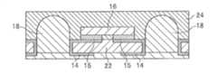
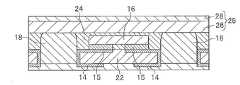
図1及び図3A〜図3Cに示すように、発光装置10は、矩形の基板22と、基板22上に実装された発光素子16と、発光素子16を覆う導光部材24と、導光部材24上に設けられた透光性部材25と、透光性部材25及び導光部材24の周囲に発光素子16を囲むように設けた反射部材17と、素子電極15と、配線14とを備えている。この発光装置10は、発光面12である透光性部材25を介して光を照射するものである。図に示した例では、この透光性部材25は、蛍光体層26及びその上に積層された透光層28を含んでいる。尚、本発明において蛍光体層26は必ずしも必須ではない。以下の説明は透光性部材25が蛍光体層26を含む場合を例として説明する。また、反射部材17は、発光素子16の側面に対向して設けられた第1反射部材18と、第1反射部材18の外側に位置し発光素子16を包囲して設けられた第2反射部材20とを有している。
以下、各構成について順次説明する。
<Light emitting device>
As shown in FIGS. 1 and 3A to 3C, thelight emitting device 10 includes arectangular substrate 22, alight emitting element 16 mounted on thesubstrate 22, alight guide member 24 that covers thelight emitting element 16, and a light guide member. 24, atranslucent member 25 provided on thereflective member 24, areflective member 17 provided around thetranslucent member 25 and thelight guide member 24 so as to surround thelight emitting element 16, anelement electrode 15, and awiring 14. ing. Thelight emitting device 10 irradiates light through the lighttransmissive member 25 which is thelight emitting surface 12. In the example shown in the figure, thetranslucent member 25 includes aphosphor layer 26 and atranslucent layer 28 laminated thereon. Thephosphor layer 26 is not always essential in the present invention. In the following description, the case where thetranslucent member 25 includes thephosphor layer 26 will be described as an example. Further, the reflectingmember 17 is provided with a first reflectingmember 18 provided to face the side surface of thelight emitting element 16, and a second reflecting member provided outside the first reflectingmember 18 and surrounding thelight emitting element 16. 20 and 20.
Hereinafter, each configuration will be sequentially described.

図3A〜図3Cに示すように、発光素子16は、透光性基板と、半導体層と、素子電極15と、を備えている。この発光素子16は、その上面視形状が、矩形、特に、長辺と短辺をもつ長方形状であることが好ましい。また、発光素子16は、その他の形状であってもよく、例えば六角形状であれば発光効率を高めることもできる。発光素子16は、同一面側に正負(p,n)電極を有することが好ましい。また、発光素子16は1つの発光装置10中に1個でもよいし、複数個含まれてもよい。なお、複数の発光素子16を含む場合は、直列又は並列に接続することができる。  As shown in FIGS. 3A to 3C, thelight emitting element 16 includes a translucent substrate, a semiconductor layer, and anelement electrode 15. It is preferable that thelight emitting element 16 has a rectangular shape in a top view, particularly a rectangular shape having a long side and a short side. Further, thelight emitting element 16 may have other shapes, for example, a hexagonal shape can enhance the light emission efficiency. Thelight emitting element 16 preferably has positive and negative (p, n) electrodes on the same surface side. Further, onelight emitting device 16 may be provided in onelight emitting device 10, or a plurality of light emittingdevices 16 may be included. When a plurality oflight emitting elements 16 are included, they can be connected in series or in parallel.

なお、透光性基板は、通常、半導体発光素子を製造する際に用いられるものであればよく、具体的には、サファイア基板が使用される。また、半導体層は、半導体層の積層体、即ち少なくともn型半導体層とp型半導体層を含み、また活性層をその間に介することが好ましい。半導体層は、その半導体材料として、波長変換物質を効率良く励起できる短波長の光を発光可能な材料である、窒化物半導体を用いることが好ましい。窒化物半導体は、主として一般式InAlGa1−x−yN(0≦x、0≦y、x+y≦1)で表される。さらに、素子電極15は、同一面側に形成されている。素子電極15は、実装が可能な金属材料である必要があるが、電気的な接続を可能とする導電部材であれば、金属の種類を特に限定する必要はない。この素子電極15は、後記する基板22と接合部材を介して接合される。Note that the translucent substrate may be any one that is usually used when manufacturing a semiconductor light emitting device, and specifically, a sapphire substrate is used. Further, it is preferable that the semiconductor layer includes a stacked body of semiconductor layers, that is, at least an n-type semiconductor layer and a p-type semiconductor layer, and an active layer interposed therebetween. As the semiconductor material of the semiconductor layer, it is preferable to use a nitride semiconductor, which is a material capable of emitting short-wavelength light capable of efficiently exciting the wavelength conversion substance. Nitride semiconductor is represented by mainly general formulaIn x Al y Ga 1-x -y N (0 ≦ x, 0 ≦ y, x + y ≦ 1). Further, thedevice electrodes 15 are formed on the same surface side. Theelement electrode 15 needs to be a mountable metal material, but the kind of metal is not particularly limited as long as it is a conductive member that enables electrical connection. Theelement electrode 15 is joined to thesubstrate 22 described later via a joining member.

接合部材は、発光素子16の素子電極15と、基板22の配線14との間に介在するように設ければよい。例えば、基板22の配線14において発光素子16を載置する領域に設けてもよく、又は、発光素子16の素子電極15側に設けてもよく、あるいは、その両方に設けてもよい。接合部材は、導電性の液状又はペースト状で、粘度等に応じてポッティング法、印刷法、転写法等の方法から適宜選択することができる。  The joining member may be provided so as to be interposed between theelement electrode 15 of thelight emitting element 16 and thewiring 14 of thesubstrate 22. For example, thewiring 14 of thesubstrate 22 may be provided in a region where thelight emitting element 16 is mounted, or may be provided on theelement electrode 15 side of thelight emitting element 16, or both of them. The joining member is a conductive liquid or paste and can be appropriately selected from methods such as a potting method, a printing method and a transfer method depending on the viscosity and the like.

基板22は、少なくとも、配線14及び配線を保持する基体と、により構成される。
配線14は、基体の少なくとも上面(前面)に形成され、基体の内部及び/又は側面及び/又は下面(後面)にも形成されていてもよい。配線14は、例えば、銅あるいは銅合金で形成することができる。また、基体は、リジッド基板であれば、樹脂若しくは繊維強化樹脂、セラミックス、ガラス、金属、紙などを用いて構成することができる。基材は、特に発光素子の線膨張係数に近い物性を有する基材を使用することが好ましい。
Thesubstrate 22 includes at least thewiring 14 and a base body that holds the wiring.
Thewiring 14 is formed on at least the upper surface (front surface) of the base, and may also be formed inside and / or on the side surface and / or on the lower surface (rear surface) of the base. Thewiring 14 can be formed of, for example, copper or a copper alloy. Further, the base can be made of resin or fiber reinforced resin, ceramics, glass, metal, paper or the like as long as it is a rigid substrate. As the base material, it is particularly preferable to use a base material having physical properties close to the linear expansion coefficient of the light emitting element.

導光部材24は、反射部材17で囲まれた領域を充填するように設けられ、基板22に搭載される発光素子16を封止する部材である。導光部材24としては、発光素子16が発する光の波長に対して良好な透光性を有し、封止部材として耐候性、耐光性及び耐熱性の良好な材料が好ましい。発光素子16の側面に導光部材24を設けることで、発光素子16の側面からの光を、より効率よく透光性部材25に導く。このことにより、光の損失を抑制して、発光装置10の光取り出し効率を向上できる。  Thelight guide member 24 is a member that is provided so as to fill the region surrounded by thereflection member 17 and seals thelight emitting element 16 mounted on thesubstrate 22. As thelight guide member 24, it is preferable to use a material having a good light-transmitting property with respect to the wavelength of the light emitted by thelight emitting element 16 and a sealing member having a good weather resistance, light resistance and heat resistance. By providing thelight guide member 24 on the side surface of thelight emitting element 16, the light from the side surface of thelight emitting element 16 is guided to thetranslucent member 25 more efficiently. As a result, the loss of light can be suppressed and the light extraction efficiency of thelight emitting device 10 can be improved.

導光部材24の材料としては、例えば、熱可塑性樹脂や熱硬化性樹脂が挙げられる。熱可塑性樹脂としては、例えば、ポリフタルアミド樹脂、液晶ポリマー、ポリブチレンテレフタレート(PBT)、不飽和ポリエステルなどを用いることができる。また、熱硬化性樹脂としては、例えば、エポキシ樹脂、変性エポキシ樹脂、シリコーン樹脂、変性シリコーン樹脂などを用いることができる。Examples of the material of thelight guide member 24 include thermoplastic resin and thermosetting resin. As the thermoplastic resin, for example, polyphthalamide resin, liquid crystal polymer, polybutylene terephthalate (PBT), unsaturated polyester and the like can be used. As the thermosetting resin, for example, an epoxy resin, a modified epoxy resin, a silicone resin, a modified silicone resin, or the like can be used.

反射部材17は、発光装置の側壁を構成し、発光素子16からの光を反射して発光面12から外部に取り出すものである。この反射部材17は、第1反射部材18と、第2反射部材20とを備えている。反射部材17は、第1反射部材18と第2反射部材20とにより光の取り出し効率を高めるものである。
反射部材17は、前方への光取り出し効率の観点から、発光素子の発光ピーク波長における光反射率が、70%以上であることが好ましく、80%以上であることがより好ましく、90%以上であることがよりいっそう好ましい。さらに、反射部材17は、白色であることが好ましい。よって、反射部材17は、母材中に白色顔料を含有してなることが好ましい。
Thereflection member 17 constitutes a side wall of the light emitting device, reflects the light from thelight emitting element 16 and takes it out from thelight emitting surface 12. The reflectingmember 17 includes a first reflectingmember 18 and a second reflectingmember 20. The reflectingmember 17 enhances the light extraction efficiency by the first reflectingmember 18 and the second reflectingmember 20.
From the viewpoint of forward light extraction efficiency, the reflectingmember 17 preferably has a light reflectance at the emission peak wavelength of the light emitting element of 70% or more, more preferably 80% or more, and 90% or more. It is even more preferred to be present. Furthermore, the reflectingmember 17 is preferably white. Therefore, the reflectingmember 17 preferably contains the white pigment in the base material.

反射部材17の母材は、樹脂を用いることができ、例えばシリコーン樹脂、エポキシ樹脂、フェノール樹脂、ポリカーボネート樹脂、アクリル樹脂、又はこれらの変性樹脂が挙げられる。なかでも、シリコーン樹脂及び変性シリコーン樹脂は、耐熱性及び耐光性に優れ、好ましい。具体的なシリコーン樹脂としては、ジメチルシリコーン樹脂、フェニル−メチルシリコーン樹脂、ジフェニルシリコーン樹脂が挙げられる。また、反射部材の母材は、上記樹脂中に各種のフィラーを含有してもよい。このフィラーとしては、酸化珪素、酸化アルミニウム、酸化ジルコニウム、酸化亜鉛などが挙げられる。フィラーは、これらのうちの1種、又はこれらのうちの2種以上を組み合わせて用いることができる。特に、熱膨張係数の小さい酸化珪素が好ましい。また、フィラーとして、ナノ粒子を用いることで、発光素子の青色光のレイリー散乱を含む散乱を増大させ、波長変換物質の使用量を低減することもできる。なお、ナノ粒子とは、粒径が1nm以上100nm以下の粒子とする。また、本明細書における「粒径」は、例えば、D50で定義される。A resin can be used for the base material of the reflectingmember 17, and examples thereof include silicone resin, epoxy resin, phenol resin, polycarbonate resin, acrylic resin, and modified resins thereof. Among them, the silicone resin and the modified silicone resin are preferable because they are excellent in heat resistance and light resistance. Specific silicone resins include dimethyl silicone resin, phenyl-methyl silicone resin, and diphenyl silicone resin. Further, the base material of the reflecting member may contain various fillers in the resin. Examples of the filler include silicon oxide, aluminum oxide, zirconium oxide, zinc oxide and the like. The filler may be used alone or in combination of two or more. In particular, silicon oxide having a small coefficient of thermal expansion is preferable. Further, by using nanoparticles as the filler, it is possible to increase scattering including blue Rayleigh scattering of the light emitting element and reduce the amount of the wavelength conversion substance used. Note that the nanoparticles are particles having a particle size of 1 nm or more and 100 nm or less. Further, the “particle size” in the present specification is defined by, for example, D50 .

白色顔料は、酸化チタン、酸化亜鉛、酸化マグネシウム、炭酸マグネシウム、水酸化マグネシウム、炭酸カルシウム、水酸化カルシウム、珪酸カルシウム、珪酸マグネシウム、チタン酸バリウム、硫酸バリウム、水酸化アルミニウム、酸化アルミニウム、酸化ジルコニウムのうちの1種、又はこれらのうちの2種以上を組み合わせて用いることができる。白色顔料の形状は、特に限定されず、不定形若しくは破砕状でもよく、流動性の観点では球状が好ましい。また、白色顔料の粒径は、例えば0.1μm以上0.5μm以下程度が挙げられ、光反射や被覆の効果を高めるためには小さい程好ましい。反射部材中の白色顔料の含有量は、適宜選択でき、光反射性及び液状時における粘度などの観点から、例えば10wt%以上80wt%以下が好ましく、20wt%以上70wt%以下がより好ましく、30wt%以上60wt%以下がよりいっそう好ましい。なお、「wt%」は、重量パーセントであり、第1反射部材18又は第2反射部材20の全重量に対する当該材料の重量の比率を表す。  White pigments include titanium oxide, zinc oxide, magnesium oxide, magnesium carbonate, magnesium hydroxide, calcium carbonate, calcium hydroxide, calcium silicate, magnesium silicate, barium titanate, barium sulfate, aluminum hydroxide, aluminum oxide and zirconium oxide. One of them can be used, or two or more of these can be used in combination. The shape of the white pigment is not particularly limited, and may be indefinite or crushed, and spherical is preferable from the viewpoint of fluidity. Further, the particle size of the white pigment is, for example, about 0.1 μm or more and 0.5 μm or less, and the smaller the better in order to enhance the effect of light reflection and coating. The content of the white pigment in the reflecting member can be appropriately selected, and from the viewpoint of light reflectivity and viscosity in a liquid state, for example, 10 wt% or more and 80 wt% or less is preferable, 20 wt% or more and 70 wt% or less is more preferable, and 30 wt% Above 60 wt% is even more preferable. In addition, "wt%" is a weight percentage and represents the ratio of the weight of the material to the total weight of the first reflectingmember 18 or the second reflectingmember 20.

第1反射部材18は、上面視において長辺と短辺を有する発光素子16を用いる場合は、発光素子16の短辺に対向する位置に設けられている。この第1反射部材18は、透光性部材25に向かって対向する間隔が拡がるように傾斜する傾斜面あるいは曲面の内側面19を有している。言い換えれば、一対の第1反射部材18のそれぞれは、それらの間の距離が照射方向Brに向かって徐々に拡がるように傾斜する傾斜面あるいは曲面の内側面19を有している。また、第1反射部材18の外側面は、第2反射部材20の内側面に当接した状態で設けられている。そして、第1反射部材18の上端部は、蛍光体層26の下面に当接した状態で設けられている。さらに、第1反射部材18は、基板22の短辺に対向する基板側面に当接し、第1反射部材18の下面が、基板22の下面と同一平面になるように設けられている。なお、第2反射部材20が設けられている位置では、第2反射部材20の下端に第1反射部材18の一部が入り込んで、第2反射部材20の下端が第1反射部材18の下端よりも高い位置になっている。第1反射部材18は、一例として、後記する第2反射部材20と同じ光反射性材料を使用している。  When using thelight emitting element 16 having a long side and a short side in a top view, the first reflectingmember 18 is provided at a position facing the short side of thelight emitting element 16. The first reflectingmember 18 has aninner surface 19 that is an inclined surface or a curved surface that is inclined so as to widen the interval facing thetranslucent member 25. In other words, each of the pair of first reflectingmembers 18 has aninner surface 19 that is an inclined surface or a curved surface that is inclined so that the distance between them gradually increases in the irradiation direction Br. The outer side surface of the first reflectingmember 18 is provided in contact with the inner side surface of the second reflectingmember 20. The upper end of the first reflectingmember 18 is provided in contact with the lower surface of thephosphor layer 26. Further, the first reflectingmember 18 is provided so as to abut on a side surface of thesubstrate 22 facing the short side of thesubstrate 22, and the lower surface of the first reflectingmember 18 is flush with the lower surface of thesubstrate 22. At the position where the second reflectingmember 20 is provided, a part of the first reflectingmember 18 enters the lower end of the second reflectingmember 20, and the lower end of the second reflectingmember 20 is the lower end of the first reflectingmember 18. It is in a higher position than. The first reflectingmember 18 uses, for example, the same light reflecting material as that of the second reflectingmember 20 described later.

第2反射部材20は、第1反射部材18及び発光素子16を囲むように設けられている。第2反射部材20は、発光装置10の側壁を形成している。第2反射部材20は、その上端部を透光性部材25の上面と同一平面になるように設け、透光性部材25の側面を覆っている。また、図3Cに示すように、第2反射部材20は、基板22の長手方向における周縁上面に当接するように設けられている。第2反射部材20の厚みはどのようなものでもよいが、図3A等では、第2反射部材20は、第1反射部材18に対して厚みが半分以下になるように設定されている。第2反射部材20は、第1反射部材18の厚みと同じか薄いほうがより好ましい。第2反射部材20を薄くすることで、発光面12を広くとることができ、取り出した光を広範囲に伝播できる。
第2反射部材20は、後記する製造方法の手順により先に第1反射部材18が設置された後に、第1反射部材18に設けた溝に充填されることで製造される。第2反射部材20は、第1反射部材18の厚みよりも薄くなるように設定されている第2反射部材20の材料と第1反射部材18の材料とは同じでも異なっていてもよい。ここでは、同じ材料として一例を説明しているので、例えば、上記で述べた反射部材を用いられることが好ましい。
The second reflectingmember 20 is provided so as to surround the first reflectingmember 18 and thelight emitting element 16. The second reflectingmember 20 forms a side wall of thelight emitting device 10. Thesecond reflection member 20 is provided such that its upper end portion is flush with the upper surface of thetranslucent member 25 and covers the side surface of thetranslucent member 25. Further, as shown in FIG. 3C, the second reflectingmember 20 is provided so as to contact the upper surface of the peripheral edge of thesubstrate 22 in the longitudinal direction. The thickness of the secondreflective member 20 may be any, but in FIG. 3A and the like, the thickness of the secondreflective member 20 is set to be half or less than that of the firstreflective member 18. It is more preferable that the thickness of the second reflectingmember 20 is equal to or smaller than that of the first reflectingmember 18. By making the second reflectingmember 20 thin, thelight emitting surface 12 can be made wide, and the extracted light can be propagated in a wide range.
The second reflectingmember 20 is manufactured by first installing the first reflectingmember 18 and then filling the groove provided in the first reflectingmember 18 by the procedure of the manufacturing method described below. The material of the second reflectingmember 20 and the material of the first reflectingmember 18 that are set to be thinner than the thickness of the first reflectingmember 18 may be the same or different. Since one example is described here as the same material, it is preferable to use the reflecting member described above, for example.

このような構成により、第1反射部材18及び第2反射部材20は、発光素子16及び蛍光体からの光の吸収を抑制できる。また、第1反射部材18及び第2反射部材20は、発光素子16及び蛍光体からの光を反射し、発光面12へ導く役割を果たす。第2反射部材20の厚みを薄くすることで、発光装置10の上面に発光面12を可能な限り広く取ることができ、光取り出し効率が改善される。  With such a configuration, the first reflectingmember 18 and the second reflectingmember 20 can suppress absorption of light from thelight emitting element 16 and the phosphor. Further, the first reflectingmember 18 and the second reflectingmember 20 play a role of reflecting the light from thelight emitting element 16 and the phosphor and guiding it to thelight emitting surface 12. By reducing the thickness of the second reflectingmember 20, thelight emitting surface 12 can be made as wide as possible on the upper surface of thelight emitting device 10, and the light extraction efficiency is improved.

蛍光体層26は、第1反射部材18と導光部材24との上面に設けられている。この蛍光体層26は、発光素子16からの光を波長変換するものである。例えば、発光素子16が青色光を発し、蛍光体層26は、蛍光体である波長変換物質が青色光の一部を例えば、黄色光に変換する。これにより、これらの光が混色した光(例えば白色光)を発光装置10から出射させることができる。なお、蛍光体層26に含有させる波長変換物質は複数種類でもよく、波長変換物質に代えて、又は加えて、上記の反射部材の母材と同様のフィラーを含有してもよい。  Thephosphor layer 26 is provided on the upper surfaces of the first reflectingmember 18 and thelight guide member 24. Thephosphor layer 26 converts the wavelength of light from thelight emitting element 16. For example, thelight emitting element 16 emits blue light, and thephosphor layer 26 converts a part of blue light into, for example, yellow light by the wavelength conversion substance which is a phosphor. Thereby, light (for example, white light) obtained by mixing these lights can be emitted from thelight emitting device 10. A plurality of types of wavelength conversion substances may be contained in thephosphor layer 26, and instead of or in addition to the wavelength conversion substance, a filler similar to the base material of the above-mentioned reflection member may be contained.

また、蛍光体層26は、含有する波長変換物質(蛍光体)として、当該分野で公知のものを使用することができる。例えば、緑〜黄色に発光するセリウムで賦活されたイットリウム・アルミニウム・ガーネット(YAG)系蛍光体、緑色に発光するセリウムで賦活されたルテチウム・アルミニウム・ガーネット(LAG)系蛍光体、緑〜赤色に発光するユーロピウム及び/又はクロムで賦活された窒素含有アルミノ珪酸カルシウム(CaO−Al−SiO)系蛍光体、青〜赤色に発光するユーロピウムで賦活されたシリケート((Sr,Ba)SiO)系蛍光体、緑色に発光するβサイアロン蛍光体、赤色に発光するCaAlSiN:Euで表されるCASN系又は(Sr,Ca)AlSiN:Euで表されるSCASN系蛍光体などの窒化物系蛍光体、赤色に発光するKSiF:Mn(KSF)系蛍光体、赤色に発光する硫化物系蛍光体などが挙げられる。Further, as the wavelength conversion substance (phosphor) contained in thephosphor layer 26, one known in the art can be used. For example, cerium-activated yttrium-aluminum-garnet (YAG) -based phosphor that emits green to yellow, cerium-activated lutetium-aluminum-garnet (LAG) -based phosphor that emits green, and green to red. europium and / or chromium activated nitrogen containing calcium aluminosilicate(CaO-Al 2 O 3 -SiO 2) based phosphor emits light, activated with europium emits blue to red silicate ((Sr,Ba) 2 SiO4 ) -based phosphors, β-sialon phosphors that emit green light, CASN-based phosphors that emit red, CaAlSiN3 : Eu, or SCASN-based phosphors that represent (Sr, Ca) AlSiN3 : Eu. Examples thereof include a nitride-based phosphor, a K2 SiF6 : Mn (KSF) -based phosphor that emits red light, and a sulfide-based phosphor that emits red light.

透光層28は、蛍光体層26からの光及び発光素子16からの光ならびに反射部材17からの光を透過して外部に取り出す。また、透光層28の上面を発光面12とする。透光層28は、蛍光体層26に当接して、かつ、その周側面を第2反射部材20に当接した状態で設けられている。透光層28の上面と第2反射部材20の上面とは同一平面となるように形成されている。透光層28は、透光性を有し、封止部材として耐候性、耐光性及び耐熱性の良好な材料が好ましい。  Thelight transmitting layer 28 transmits the light from thephosphor layer 26, the light from thelight emitting element 16 and the light from the reflectingmember 17, and takes them out to the outside. In addition, the upper surface of thetransparent layer 28 is thelight emitting surface 12. Thetranslucent layer 28 is provided in contact with thephosphor layer 26 and its peripheral side surface in contact with the second reflectingmember 20. The upper surface of thelight transmitting layer 28 and the upper surface of the second reflectingmember 20 are formed so as to be flush with each other. It is preferable that the light-transmittinglayer 28 has a light-transmitting property and that the sealing member is made of a material having good weather resistance, light resistance, and heat resistance.

なお、ここで述べる「透光性」とは、発光素子の発光ピーク波長における光透過率が、好ましくは60%以上であること、より好ましくは70%以上であること、よりいっそう好ましくは80%以上であることを言う。透光層28の母材は、シリコーン樹脂、エポキシ樹脂、フェノール樹脂、ポリカーボネート樹脂、アクリル樹脂、又はこれらの変性樹脂を用いることができる。透光層28の母材は、ガラスでもよい。なかでも、透光層28の母材は、シリコーン樹脂及び変性シリコーン樹脂は、耐熱性及び耐光性に優れ、好ましい。具体的なシリコーン樹脂としては、ジメチルシリコーン樹脂、フェニル−メチルシリコーン樹脂、ジフェニルシリコーン樹脂が挙げられる。透光性部材25は、これらの母材のうちの1種、若しくはこれらの母材のうちの2種以上を積層して構成することができる。また、透光層28の母材は、上記樹脂若しくはガラス中に上記の第1反射部材18及び第2反射部材20の母材と同様のフィラーを含有してもよい。The term "translucency" as used herein means that the light transmittance of the light emitting element at the emission peak wavelength is preferably 60% or more, more preferably 70% or more, and even more preferably 80%. Say that is above. As the base material of thetranslucent layer 28, silicone resin, epoxy resin, phenol resin, polycarbonate resin, acrylic resin, or modified resin thereof can be used. The base material of thetransparent layer 28 may be glass. Among them, the base material of the light-transmittinglayer 28 is preferably a silicone resin or a modified silicone resin, which is excellent in heat resistance and light resistance. Specific silicone resins include dimethyl silicone resin, phenyl-methyl silicone resin, and diphenyl silicone resin. Thetranslucent member 25 can be configured by one of these base materials or by laminating two or more of these base materials. The base material of thetranslucent layer 28 may contain the same filler as the base material of the first reflectingmember 18 and the second reflectingmember 20 in the resin or glass.

発光装置10は、以上のように構成されているので、発光素子16から光が照射されると、導光部材24を透過して透光性部材25(蛍光体層26及び透光層28)を通過し発光面12から外部に取り出される。また、発光素子16からの光の一部は、第1反射部材18の傾斜面あるいは湾曲の内側面19により発光面12側に取り出され易くなる。また、第2反射部材20は、蛍光体層26及び透光層28の側面を覆っていることで、第2反射部材20により反射して光が、発光面12から取り出されることになる。  Since thelight emitting device 10 is configured as described above, when the light is emitted from thelight emitting element 16, thelight transmitting member 25 transmits the light transmitting member 25 (thephosphor layer 26 and the light transmitting layer 28). And is taken out from thelight emitting surface 12. In addition, a part of the light from thelight emitting element 16 is easily extracted to thelight emitting surface 12 side by the inclined surface or the curvedinner side surface 19 of the first reflectingmember 18. Further, since the second reflectingmember 20 covers the side surfaces of thephosphor layer 26 and thelight transmitting layer 28, the light is reflected by the second reflectingmember 20 and the light is extracted from thelight emitting surface 12.

なお、第1反射部材18は、所要の厚み(例えば、基板22と同等かそれ以上の厚み)があり、基板22と共に発光装置10の枠体を形成して発光装置全体の強度を維持している。そして、第1反射部材18の上端部よりも上に蛍光体層26及び透光層28を配置することで、発光装置10の上面に発光面12を可能な限り広く取ることができる。さらに、第1反射部材18の上部に傾斜面又は湾曲の内側面19が形成されていることで、発光素子16からの光を発光面12から取り出し易くなる。したがって、発光装置10は、光取り出し効率が改善され、色調ムラも緩和される。  The first reflectingmember 18 has a required thickness (for example, equal to or more than the substrate 22), and forms the frame of thelight emitting device 10 together with thesubstrate 22 to maintain the strength of the entire light emitting device. There is. By disposing thephosphor layer 26 and thetranslucent layer 28 above the upper end portion of the first reflectingmember 18, thelight emitting surface 12 can be as wide as possible on the upper surface of thelight emitting device 10. Further, since the inclined surface or the curvedinner side surface 19 is formed on the upper portion of the first reflectingmember 18, the light from thelight emitting element 16 can be easily extracted from thelight emitting surface 12. Therefore, in thelight emitting device 10, the light extraction efficiency is improved and the unevenness of color tone is alleviated.

<発光装置の製造方法>
次に、第1実施形態に係る発光装置の製造方法について以下に説明する。
図4に示すように、発光装置の製造方法は、発光素子16を配列する工程S101と、第1反射部材18を設ける工程S102と、導光部材24を設ける工程S103と、透光性部材25を設ける工程S105と、第1溝32を形成する工程S106と、第2反射部材20を設ける工程S108と、個片化する工程S109を含む手順で行われる。なお、発光装置の製造方法では、導光部材24を設ける工程S103の後に除去する工程S104を行うこととしてもよく、さらに、第1溝32を形成する工程S106の次に第2溝34を形成する工程S107を行うこととしてもよい。以下各工程について説明する。
<Method of manufacturing light emitting device>
Next, a method for manufacturing the light emitting device according to the first embodiment will be described below.
As shown in FIG. 4, in the method for manufacturing the light emitting device, the step S101 of arranging thelight emitting elements 16, the step S102 of providing the first reflectingmember 18, the step S103 of providing thelight guide member 24, and thetranslucent member 25. Is performed in a procedure including a step S105 of providing thefirst groove 32, a step S106 of forming thefirst groove 32, a step S108 of providing the second reflectingmember 20, and a step S109 of dividing into individual pieces. In the method for manufacturing the light emitting device, the removing step S104 may be performed after the step S103 of providing thelight guide member 24, and thesecond groove 34 is formed after the step S106 of forming thefirst groove 32. The step S107 of performing may be performed. Each step will be described below.

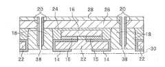
最初に、図4及び図5Aに示すように、発光素子16を配列する工程S101では、配線14が形成された基板22上に複数の発光素子16を配列する。発光素子16を配列する場合には、接合部材を介してフリップチップ実装で行われることが好ましい。発光素子16は、行方向及び列方向に複数が所定の間隔を空けて配列される。配列された発光素子16は、列側の間隔が行側の間隔よりも大きくなるように配置されている。また、基板22は、列側に貫通穴22aが形成されている。貫通穴22aは、行方向、詳細には、発光素子16の短辺に対向する位置に連続して形成され、基板22の周縁には形成されていない。また、基板22は、その裏面に粘着シート30が貼り付けられた状態で作業が行われる。  First, as shown in FIGS. 4 and 5A, in step S101 of arranging thelight emitting elements 16, the plurality oflight emitting elements 16 are arranged on thesubstrate 22 on which thewiring 14 is formed. When thelight emitting elements 16 are arranged, it is preferable that thelight emitting elements 16 are mounted by flip chip mounting via a joining member. A plurality of thelight emitting elements 16 are arranged at predetermined intervals in the row direction and the column direction. The arrayedlight emitting elements 16 are arranged such that the spacing on the column side is larger than the spacing on the row side. Further, thesubstrate 22 has throughholes 22a formed on the row side. The through holes 22 a are continuously formed in the row direction, specifically, at a position facing the short side of thelight emitting element 16, and are not formed in the peripheral edge of thesubstrate 22. In addition, the work is performed with theadhesive sheet 30 attached to the back surface of thesubstrate 22.

第1反射部材18を設ける工程S102では、基板22上に行方向及び列方向に配列された発光素子16において、列方向に並ぶ発光素子16の列間に第1反射部材18を設ける。言い換えると、図5Aにおいて、列方向に形成された貫通穴22a内に第1反射部材18を設ける。詳細には、図5Bに示すように、基板22の上に搭載された発光素子16の短辺に対向する両側に、第1反射部材18が設けられる。
この第1反射部材18は、予め粘度が調整されており、貫通穴22a内に入り込んだ状態で、基板22の上面若しくはそれ以上の高さを維持するように、発光素子16から離間して設けられる。基板22には、第1反射部材18が設けられる領域に沿って貫通穴22aが予め設けられ、基板22の下面側に、貫通穴22aの開口を塞ぐように粘着シート30で塞がれている。そのため、第1反射部材18の下面は、基板22の下面と同一平面となるように形成される。また、第1反射部材18の上部には、表面張力や粘性により傾斜面あるいは曲面となる部分が形成される。第1反射部材18は、発光素子16の上端よりも高くなるように設けられる。なお、第1反射部材18を設けるときに所定の形状、高さとなるようにガイドを基板上に配置した状態とし、第1反射部材18が硬化したら配置したガイドを除去することとしてもよい。第1反射部材18は、トランスファ成形、射出成形、圧縮成形、ポッティングなどにより形成することができる。
In the step S102 of providing the first reflectingmember 18, in thelight emitting elements 16 arranged in the row direction and the column direction on thesubstrate 22, the first reflectingmember 18 is provided between the columns of thelight emitting elements 16 arranged in the column direction. In other words, in FIG. 5A, the first reflectingmember 18 is provided in the throughhole 22a formed in the column direction. Specifically, as shown in FIG. 5B, the first reflectingmember 18 is provided on both sides of thelight emitting element 16 mounted on thesubstrate 22 so as to face the short side.
The first reflectingmember 18 has a viscosity adjusted in advance, and is provided separately from thelight emitting element 16 so as to maintain the height of the upper surface of thesubstrate 22 or higher while being in the throughhole 22a. Be done. Thesubstrate 22 is provided with a throughhole 22a in advance along a region where the first reflectingmember 18 is provided, and the lower surface of thesubstrate 22 is covered with anadhesive sheet 30 so as to close the opening of the throughhole 22a. .. Therefore, the lower surface of the first reflectingmember 18 is formed so as to be flush with the lower surface of thesubstrate 22. Further, on the upper part of the first reflectingmember 18, a portion which becomes an inclined surface or a curved surface due to surface tension and viscosity is formed. The first reflectingmember 18 is provided so as to be higher than the upper end of thelight emitting element 16. In addition, when the first reflectingmember 18 is provided, the guide may be placed on the substrate so as to have a predetermined shape and height, and the placed guide may be removed when the first reflectingmember 18 is cured. The first reflectingmember 18 can be formed by transfer molding, injection molding, compression molding, potting, or the like.

次に、図4及び図5Cに示すように、導光部材を設ける工程S103では、第1反射部材18と発光素子16との間の空間、及び、発光素子16同士の空間が導光部材24で満たされるように充填される。ここでは、導光部材24は、第1反射部材18及び発光素子16が埋まる高さまで充填して硬化させる。なお、導光部材24は、硬化させるときに、熱硬化性樹脂である場合には加熱、紫外線硬化性樹脂であるときには紫外線の照射を積極的に行うことが好ましい。充填方法としては、トランスファ成形、射出成形、圧縮形成、ポッティング等が挙げられる。  Next, as shown in FIGS. 4 and 5C, in the step S103 of providing the light guide member, the space between the first reflectingmember 18 and thelight emitting element 16 and the space between thelight emitting elements 16 are thelight guide member 24. Is filled so that it is filled with. Here, thelight guide member 24 is filled and cured to a height at which the first reflectingmember 18 and thelight emitting element 16 are filled. When thelight guide member 24 is cured, it is preferable to positively perform heating when it is a thermosetting resin and irradiation of ultraviolet rays when it is an ultraviolet curing resin. Examples of the filling method include transfer molding, injection molding, compression molding, potting and the like.

図4及び図5Dに示すように、除去する工程S104では、発光素子16の上方に導光部材24が位置するように残し、第1反射部材18の上部の一部が除去される高さまで導光部材24と第1反射部材18とが平坦になるよう除去される。なお、除去するときには砥石による研磨、円盤状の回転刃、鉋等で導光部材24及び第1反射部材18とが除去されることとしてもよい。  As shown in FIGS. 4 and 5D, in the removing step S104, thelight guide member 24 is left above thelight emitting element 16 and is guided to a height at which a part of the upper portion of the first reflectingmember 18 is removed. Thelight member 24 and the first reflectingmember 18 are removed so as to be flat. In addition, when removing, thelight guide member 24 and the first reflectingmember 18 may be removed by polishing with a grindstone, a disk-shaped rotary blade, a plane, or the like.

その後、図4及び図5Eに示すように、透光性部材を設ける工程S105では、予め蛍光体を含有する蛍光体層26になるシート部材と、透光層28となるシート部材とを重ねた透光性部材25であるシート部材を、透光性の接合部材を介して、導光部材24及び第1反射部材18の上面に設けられる。なお、図5Eにおいて、蛍光体層26のシート部材は、透光層28のシート部材よりも厚く形成されているがこれに限らない。蛍光体層26と透光層28は、同じ厚さでもいいし、透光層28が蛍光体層26より厚く形成されてもよい。また、上記ではシート状の透光性部材25を使用しているが、これには限らない。液状の透光性部材25を噴霧しても形成してもいいし、印刷等で形成してもよい。  Thereafter, as shown in FIG. 4 and FIG. 5E, in the step S105 of providing the translucent member, the sheet member which becomes thephosphor layer 26 containing the phosphor in advance and the sheet member which becomes thetranslucent layer 28 are superposed. The sheet member that is thetranslucent member 25 is provided on the upper surfaces of thelight guide member 24 and the first reflectingmember 18 via the translucent joining member. 5E, the sheet member of thephosphor layer 26 is formed thicker than the sheet member of thetranslucent layer 28, but the present invention is not limited to this. Thephosphor layer 26 and thetranslucent layer 28 may have the same thickness, or thetranslucent layer 28 may be formed thicker than thephosphor layer 26. Further, although the sheet-shapedtranslucent member 25 is used in the above, the present invention is not limited to this. The liquidtranslucent member 25 may be sprayed or formed, or may be formed by printing or the like.

続いて、図4、図5F及び図6Aに示すように、第1溝32を形成する工程S106では、第1反射部材18の中心を通るように、透光性部材25(蛍光体層26及びその上に積層された透光層28)と第1反射部材18の一部を除去して所定溝幅の第1溝32が、円盤状の回転刃等よりダイシングされ、形成される。ここで、第1溝32の深さは、透光性部材25を貫通し、第1溝32の先端が第1反射部材18内にあるのがよい。次工程である第1溝32内に第2反射部材20を設ける工程S108において、透光性部材25の側面すべてを第2反射部材20で覆うことができる。これにより、個片化する工程S109で個片化した時に、透光性部材25側面からの色漏れを防止できる。  Subsequently, as shown in FIG. 4, FIG. 5F, and FIG. 6A, in step S106 of forming thefirst groove 32, the translucent member 25 (thephosphor layer 26 and By removing a part of the transparent layer 28) and the first reflectingmember 18 laminated thereon, thefirst groove 32 having a predetermined groove width is formed by dicing with a disc-shaped rotary blade or the like. Here, the depth of thefirst groove 32 is preferably such that it penetrates thetransparent member 25 and the tip of thefirst groove 32 is inside the first reflectingmember 18. In step S108 of providing the second reflectingmember 20 in thefirst groove 32, which is the next step, all the side surfaces of thetranslucent member 25 can be covered with the second reflectingmember 20. This prevents color leakage from the side surface of thetranslucent member 25 when individualized in the step S109 of individualizing.

第1溝32は、第1反射部材18の中心を移動しながら回転するブレードを用いた加工装置により行われる。なお、第1溝32を形成する場合には、基板22を載置しているテーブルをX方向及びX方向に直交するY方向に移動させ加工装置は、固定して加工作業を行うことや、テーブルは固定して加工装置を移動して加工作業を行うことのどちらであってもよい。また、ここでは、第1溝32に直交する方向である行方向に、第2溝を形成する工程S107を行っている。第2溝34は、2次元的に配列された多数の発光素子16の行間に対して形成される。なお、第2溝34は透光性部材25と導光部材24を貫通して基板22まで到達するように形成されることが好ましい。これにより、次工程である第2反射部材を設ける工程S108において、行間側の導光部材24全体が第2反射部材20で覆われ、導光部材24からの外部への色抜けを防止できる。Thefirst groove 32 is formed by a processing device that uses a blade that rotates while moving along the center of the first reflectingmember 18. When forming thefirst groove 32, the table on which thesubstrate 22 is placed is moved in the X direction and the Y direction orthogonal to the X direction, and the processing device is fixed to perform the processing operation. The table may be fixed and the processing device may be moved to perform the processing operation. Further, here, the step S107 of forming the second groove is performed in the row direction which is a direction orthogonal to thefirst groove 32. Thesecond groove 34 is formed between rows of the plurality oflight emitting elements 16 arranged two-dimensionally. Thesecond groove 34 is preferably formed so as to penetrate thetranslucent member 25 and thelight guide member 24 and reach thesubstrate 22. As a result, in the next step of providing the second reflecting member S108, the entirelight guide member 24 on the inter-row side is covered with the second reflectingmember 20, and color loss from thelight guide member 24 to the outside can be prevented.

そして、図4、図5G及び図6Bに示すように、第2反射部材を設ける工程S108では、第1溝32内、及び第2溝34内に第2反射部材20がトランスファ成形、射出成形、圧縮成形、ポッティング等で充填される。第2反射部材20は、一例として、第1反射部材18と同じ材料で形成されている。なお、ここでは、第2反射部材20が硬化した後に、透光層28のシート部材及び第2反射部材20の厚みを調整するために除去加工を行っている。ここでは、透光層28が平坦で所定の厚みになるように除去加工が行われる。  Then, as shown in FIGS. 4, 5G, and 6B, in the step S108 of providing the second reflecting member, the second reflectingmember 20 is transferred into thefirst groove 32 and thesecond groove 34 by transfer molding, injection molding, Filled by compression molding, potting, etc. The second reflectingmember 20 is formed of the same material as the first reflectingmember 18, for example. In addition, here, after the secondreflective member 20 is cured, a removal process is performed in order to adjust the thickness of the sheet member of thetranslucent layer 28 and the secondreflective member 20. Here, the removal processing is performed so that thelight transmitting layer 28 is flat and has a predetermined thickness.

最後に、図4、図5H及び図6Cに示すように、個片化する工程S109では、第2反射部材20の中心を行列方向に加工装置により、粘着シート30に到達するまで円盤状の回転刃、超音波カッターの切断刃、押し切り型のカッター等でダイシングして、切溝38を形成する。個片化する工程S109は、第1溝32及び第2溝34を形成したときよりも幅の狭いブレードが使用されて加工作業が行われる。個片化されることにより1つ1つの発光装置10が粘着シート30に接着している状態となっている。そして、粘着シート30を剥がすことにより、個々の発光装置10となる。
なお、発光装置10では、第1反射部材18が、基板22と同一位置に下面が位置するように構成されている。そのため、このような発光装置10の構成では、反射部材17の部分を円盤状の回転刃、超音波カッターの切断刃、押し切り型のカッター等でダイシングすることで個片化することとなり、基板22の切断をすることがなく、個片化を容易にすることができる。
Lastly, as shown in FIGS. 4, 5H, and 6C, in the step S109 of dividing into pieces, the center of the second reflectingmember 20 is rotated in a disk shape by a processing device until theadhesive sheet 30 is reached. A cuttinggroove 38 is formed by dicing with a blade, a cutting blade of an ultrasonic cutter, a push-cut type cutter, or the like. In the step S109 of dividing into individual pieces, a working operation is performed by using a blade having a width narrower than that when thefirst groove 32 and thesecond groove 34 are formed. The individuallight emitting devices 10 are bonded to theadhesive sheet 30 by being separated into individual pieces. Then, theadhesive sheet 30 is peeled off to form the individuallight emitting devices 10.
In thelight emitting device 10, the first reflectingmember 18 is configured such that the lower surface is located at the same position as thesubstrate 22. Therefore, in such a configuration of thelight emitting device 10, the portion of thereflection member 17 is diced by a disk-shaped rotary blade, a cutting blade of an ultrasonic cutter, a push-cut type cutter, or the like to be diced into individual pieces. It is possible to facilitate individualization without cutting.

<第2実施形態>
次に、発光装置の第2実施形態について図7及び図8を中心に説明する。なお、第1実施形態と同じ構成については同じ符号を付して説明を適宜省略する。
図7に示すように、発光装置10Aは、基板22上の第1反射部材18と発光素子16の間の領域に第3反射部材36を発光素子16の長辺及び/もしくは短辺に対向して設けている。第3反射部材36は、第1反射部材18の内側面に接し透光性部材25に向かって対向する間隔が拡がるように傾斜する傾斜面あるいは曲面の内側面を有している。言い換えれば第3反射部材36のそれぞれは、第1反射部材18の内側面に接し、対向する間の距離が照射方向Brに向かって徐々に拡がるように傾斜する傾斜面あるいは曲面の内側面を有している。
この第3反射部材36は、発光素子16の高さよりも低くなるように設けられている。そして、第3反射部材36は、発光素子16から離間するように設けられている。第3反射部材36は、第1反射部材18及び第2反射部材20と同じ材料で形成されることや、あるいは、異なる材料で形成されることとしてもよい。第3反射部材36を設けることにより、基板22の上面での光の吸収が減少するとともに光が発光面12へ適切に導かれて、光取り出し効率をさらに改善することができる。
<Second Embodiment>
Next, a second embodiment of the light emitting device will be described focusing on FIGS. 7 and 8. The same components as those in the first embodiment are designated by the same reference numerals and description thereof will be omitted as appropriate.
As shown in FIG. 7, in thelight emitting device 10A, the third reflectingmember 36 is provided on thesubstrate 22 in a region between the first reflectingmember 18 and thelight emitting element 16 so as to face the long side and / or the short side of thelight emitting element 16. Are provided. The third reflectingmember 36 has an inclined or curved inner surface that is in contact with the inner surface of the first reflectingmember 18 and widens the interval facing thetranslucent member 25. In other words, each of the third reflectingmembers 36 has an inclined surface or an inner surface of a curved surface that is in contact with the inner surface of the first reflectingmember 18 and is inclined so that the distance between the third reflectingmembers 36 gradually increases in the irradiation direction Br. is doing.
The third reflectingmember 36 is provided so as to be lower than the height of thelight emitting element 16. The third reflectingmember 36 is provided so as to be separated from thelight emitting element 16. The third reflectingmember 36 may be made of the same material as the first reflectingmember 18 and the second reflectingmember 20, or may be made of a different material. By providing the third reflectingmember 36, the absorption of light on the upper surface of thesubstrate 22 is reduced and the light is appropriately guided to thelight emitting surface 12, so that the light extraction efficiency can be further improved.

発光装置10Aは、図4で示す各工程の内、第1反射部材を設ける工程S102を行った後で、導光部材を設ける工程S103を行う前に、第3反射部材を設ける工程を行うことにより製造される。すなわち、図8に示すように、第3反射部材を設ける工程は、第1反射部材18の内側に列方向に沿って第3反射部材36を設けている。第3反射部材36は、予め設定された粘度に調整され、発光面12に向かって傾斜面あるいは曲面を形成することとなる。第3反射部材を設ける工程を行った後には、導光部材を設ける工程S103を行い、その後の工程は、図4に示す通りとなる。  Among the steps shown in FIG. 4, thelight emitting device 10A performs the step of providing the third reflecting member after performing the step S102 of providing the first reflecting member and before performing the step S103 of providing the light guide member. Manufactured by. That is, as shown in FIG. 8, in the step of providing the third reflecting member, the third reflectingmember 36 is provided inside the first reflectingmember 18 along the column direction. The third reflectingmember 36 is adjusted to have a preset viscosity and forms an inclined surface or a curved surface toward thelight emitting surface 12. After performing the step of providing the third reflecting member, step S103 of providing the light guide member is performed, and the subsequent steps are as shown in FIG.

次に、図9から図12を参照して第3実施形態から第6実施形態について説明する。なお、既に説明した同じ部品には同じ符号を付して説明を適宜省略する。
<第3実施形態>
図9に示すように、発光装置10Bでは、第1反射部材の下面と基板2の下面とは同一平面になるように形成される。詳細には、基板22の下面となる配線14の下端が第1反射部材18と同一平面となるように形成される。なお、既に説明した他の実施形態においても基板22の下面が第1反射部材18と同一平面として形成することが好ましい。これにより、発光装置は、実装時に安定し、傾きにくくなり実装精度を上げることができる。
なお、配線14は、基板22の下面側において、一方と他方の長さを変えて設定されてもよい。配線14の長短が極性を示すことで、発光装置10Bを外部の装置に接続するときに間違いを防止し易くなる。
Next, the third to sixth embodiments will be described with reference to FIGS. 9 to 12. In addition, the same reference numerals are given to the same components that have already been described, and description thereof will be appropriately omitted.
<Third Embodiment>
As shown in FIG. 9, in thelight emitting device 10B, the lower surface of the first reflecting member and the lower surface of the substrate 2 are formed so as to be flush with each other. Specifically, the lower end of thewiring 14, which is the lower surface of thesubstrate 22, is formed so as to be flush with the first reflectingmember 18. In addition, also in the other embodiments already described, it is preferable that the lower surface of thesubstrate 22 is formed on the same plane as the first reflectingmember 18. Thus, the light emitting device is stable during mounting, it is possible to increase the actualSoTadashi degree hardly slope.
Thewiring 14 may be set on the lower surface side of thesubstrate 22 by changing the lengths of one side and the other side. Since the length of thewiring 14 indicates the polarity, it becomes easy to prevent an error when thelight emitting device 10B is connected to an external device.

<第4実施形態>
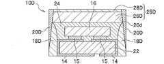
図10に示すように、発光装置10Cでは、配線14について、基板22に貫通穴を形成して作成するビア114を介する構成としてもよい。ビア114は、基板22の厚み方向に形成した貫通穴の内周面に設けた円筒形状の内壁面配線114aと、内壁面配線114a内に設けた充填部材114bとを備えている。ビア114の内壁面配線114aは、既に説明した配線14と同様の部材を使用することができる。そして、内壁面配線114aは、基板22の上面の配線14を介して素子電極15に導通するとともに、基板22の下面に形成された配線14に接続する。また、ビア114の充填部材114bは、例えば、エポキシ樹脂等の絶縁性部材が充填されることで形成される。なお、充填部材114bは、基板22の厚みの寸法よりも長い寸法に形成されている。そして、配線14は、予め基板22の上面及び下面の所定範囲に設けられ充填部材114bの上下端において周囲に位置し内壁面配線114aに導通するベース配線14aと、このベース配線14aに対面し充填部材114bを覆うとともに素子電極15に導通する接続配線14bにより形成されている。なお、配線14は、基板22の上面側及び下面側において、素子電極15に対応してそれぞれ独立するように設けられ、内壁面配線114aにより対向する上下の配線14が導通するように形成されている。
なお、発光装置10Cでは、第1反射部材18の下面が、基板22の上面に接するように設置されている。そして、第1反射部材18の上面は、発光素子16の上面よりも高い位置になるように形成されている。また、発光装置10Cは、第2反射部材20が基板22の厚み方向の中央側から透光性部材25の上面までの範囲に形成されている。
<Fourth Embodiment>
As shown in FIG. 10, in thelight emitting device 10C, thewiring 14 may be configured to include a via 114 formed by forming a through hole in thesubstrate 22. The via 114 includes a cylindrical innerwall surface wiring 114a provided on the inner peripheral surface of a through hole formed in the thickness direction of thesubstrate 22 and a fillingmember 114b provided in the innerwall surface wiring 114a. For the innerwall surface wiring 114a of the via 114, the same member as thewiring 14 already described can be used. Then, the inner wall surface wiring 114 a is electrically connected to theelement electrode 15 via thewiring 14 on the upper surface of thesubstrate 22 and connected to thewiring 14 formed on the lower surface of thesubstrate 22. The fillingmember 114b of thevia 114 is formed by filling an insulating member such as epoxy resin. The fillingmember 114b is formed to have a dimension longer than the thickness of thesubstrate 22. Thewiring 14 is provided in a predetermined range on the upper surface and the lower surface of thesubstrate 22 in advance and is located around the upper and lower ends of the fillingmember 114b and is electrically connected to the innerwall surface wiring 114a. It is formed by theconnection wiring 14b which covers themember 114b and is electrically connected to theelement electrode 15. Thewirings 14 are provided independently on the upper surface side and the lower surface side of thesubstrate 22 corresponding to theelement electrodes 15, and are formed such that the upper andlower wirings 14 facing each other are electrically connected by the innerwall surface wiring 114a. There is.
In thelight emitting device 10C, the lower surface of the first reflectingmember 18 is installed so as to contact the upper surface of thesubstrate 22. The upper surface of the first reflectingmember 18 is formed so as to be higher than the upper surface of thelight emitting element 16. Further, in thelight emitting device 10C, the second reflectingmember 20 is formed in a range from the center side in the thickness direction of thesubstrate 22 to the upper surface of thetranslucent member 25.

<第5実施形態>
図11に示すように、発光装置10Dは、第2反射部材20Dが透光性部材25Dに向かって対向する間隔が狭くなるように傾斜する傾斜面20dを有するように形成されている。第2反射部材20Dは、例えば、第1反射部材18Dの高さ方向の中段から透光性部材25Dの上面まで、断面形状が三角形に形成される。第2反射部材20Dが形成されることで、第1反射部材18Dは、第2反射部材20Dと対面する部分が傾斜面となる。また、蛍光体層26D及び透光層28Dは、第2反射部材20Dが形成されることで、断面形状が台形となる。なお、第2反射部材20Dは、透光性部材25Dの上部側面を所定の厚みに形成することができるので、発光装置10Dが他の部品に接触すること等による透光性部材25Dの破損の抑制をより向上させることができる。
なお、発光装置10Dを製造する場合には、図5Fを参照すると、第2反射部材20Dを設けるための第1溝32を断面形状がV字形状にすることで形成できる。なお、第2反射部材20Dは、透光性部材25D側の厚みが大きく、基板22側に向かうにしたがって厚みが小さくなるように設定されていれば、断面形状は台形や三角形あるいは階段状であってもよい。
<Fifth Embodiment>
As shown in FIG. 11, thelight emitting device 10D is formed so as to have aninclined surface 20d that is inclined so that the interval at which the second reflectingmember 20D faces thetranslucent member 25D becomes narrow. The second reflectingmember 20D has, for example, a triangular cross-sectional shape from the middle step in the height direction of the first reflectingmember 18D to the upper surface of thetranslucent member 25D. By forming the second reflectingmember 20D, the first reflectingmember 18D has an inclined surface at a portion facing the second reflectingmember 20D. Further, thefluorescent material layer 26D and thetranslucent layer 28D have a trapezoidal cross-sectional shape due to the formation of the second reflectingmember 20D. Since the second reflectingmember 20D can have the upper side surface of thetranslucent member 25D formed to have a predetermined thickness, damage to thetranslucent member 25D due to contact of thelight emitting device 10D with another component or the like can be prevented. The suppression can be further improved.
When manufacturing thelight emitting device 10D, referring to FIG. 5F, thefirst groove 32 for providing the second reflectingmember 20D can be formed by forming the V-shaped cross section. The second reflectingmember 20D has a trapezoidal shape, a triangular shape, or a step shape in cross section as long as the second reflectingmember 20D is set to have a large thickness on thetransparent member 25D side and a thickness that decreases toward thesubstrate 22 side. May be.

<第6実施形態>
図12に示すように、発光装置10Eは、第4実施形態で示す発光装置10Cにおいて、発光素子16を複数(図面では2つ)備えるように形成されている。発光装置10Eでは、設けられている2つの発光素子16を同時に点灯及び消灯の動作を行わせるために、配線14の一方のベース配線14aが、互いに導通するように導通配線14cにより接続されるように形成されている。なお、他の実施形態の発光装置であっても、発光装置10Eと同様に複数の発光素子16を備える構成としてもよい。
<Sixth Embodiment>
As shown in FIG. 12, thelight emitting device 10E is formed so as to include a plurality of light emitting elements 16 (two in the drawing) in thelight emitting device 10C shown in the fourth embodiment. In thelight emitting device 10E, onebase wiring 14a of thewiring 14 is connected by theconduction wiring 14c so as to be electrically connected to each other in order to simultaneously turn on and off the twolight emitting elements 16 provided. Is formed in. Note that the light emitting device of another embodiment may have a configuration including a plurality oflight emitting elements 16 as in thelight emitting device 10E.

さらに、以上説明した第1実施形態〜第6実施形態において、第2反射部材20,20Dは、第1反射部材18、18Dと比較して、部材の強度を大きくする、あるいは、部材の硬度を大きくすることがより好ましい。つまり、第2反射部材20,20Dの部分は、外部の他の部品、例えば、導光板と接触し易いため、過度な負荷が加わっても、部材強度あるは部材硬度が大きいことで、変形や欠けの破損を抑制することができる。ここで、部材の硬度を大きくする場合は、第1反射部材及び第2反射部材のベースの樹脂が同じであっても、例えば、含有する酸化チタン等の含有材料の添加量を変えることで硬度を大きくできる。また、同じシリコーン樹脂を使用する場合であっても、硬度の異なるものを選択して、硬度の高いシリコーン樹脂を第2反射部材20,20Dとして使用する。さらに、第2反射部材20,20Dと、第1反射部材18、18Dと、を異なる樹脂にすることで、硬度を変えることができる。例えば、シリコーン樹脂を第1反射部材18、18Dに使用し、シリコーン樹脂よりも一般的に硬度が大きなエポキシ樹脂を第2反射部材20,20Dに使用する。  Further, in the first to sixth embodiments described above, the second reflectingmembers 20 and 20D increase the strength of the members or increase the hardness of the members as compared with the first reflectingmembers 18 and 18D. It is more preferable to increase the size. In other words, since the second reflectingmembers 20 and 20D easily come into contact with other external components, for example, the light guide plate, even if an excessive load is applied, the member strength or the member hardness is large, which may cause deformation or deformation. It is possible to suppress breakage of the chip. Here, when increasing the hardness of the member, even if the base resin of the first reflecting member and the second reflecting member are the same, for example, the hardness can be changed by changing the addition amount of the contained material such as titanium oxide. Can be increased. Even when the same silicone resin is used, those having different hardnesses are selected and the silicone resin having high hardness is used as the second reflectingmembers 20 and 20D. Further, the hardness can be changed by using different resins for the second reflectingmembers 20 and 20D and the first reflectingmembers 18 and 18D. For example, a silicone resin is used for the first reflectingmembers 18 and 18D, and an epoxy resin that is generally harder than the silicone resin is used for the second reflectingmembers 20 and 20D.

また、部材の強度が大きい場合とは、例えば、ベースとなる樹脂が同じシリコーン樹脂の場合、引張り強度を比較して引張り強度が大きなシリコーン樹脂を言う。さらに、部材の強度が大きい場合とは、例えば、ベースとなる樹脂が同じエポキシ樹脂の場合、曲げ強度を比較して曲げ強度が大きなエポキシ樹脂を言う。なお、樹脂の種類が異なる場合は、例えば、一方がシリコーン樹脂で他方がエポキシ樹脂であるときには、曲げ強度と引張り強度とにおいて一方の強度に換算して比較することで強度の大小を判定することとする。
なお、部材の硬度あるいは部材の強度を判定する場合には、JIS等、公知の測定方法により測定することで判定することができる。また、部材の強度は、変形や破壊に対する抵抗力をいうものである。
Further, when the strength of the member is high, for example, in the case where the base resin is the same silicone resin, the tensile strength is compared and the tensile strength is high. Further, when the strength of the member is high, for example, when the base resin is the same epoxy resin, the bending strength is compared and the epoxy resin having a large bending strength is referred to. When the types of resin are different, for example, when one is a silicone resin and the other is an epoxy resin, it is possible to determine the magnitude of the strength by converting and comparing one of the bending strength and the tensile strength. And
The hardness of the member or the strength of the member can be determined by a known measurement method such as JIS. Further, the strength of a member refers to the resistance to deformation and breakage.

<変形例について>
なお、各実施形態では、基板22に貫通穴22aを形成して第1反射部材18の下面と基板22の下面を同一平面とすることとして説明したが、図13Aに示すように、第1反射部材18の一部の下面が基板22の下面と同一平面となるように形成してもよい。ここでは、第1反射部材18の左右の端部が基板22の上面に当接した状態で、第1反射部材18の中央の端部が基板22の下面と同一平面となるように設けるようにしている。このように第1反射部材18の下面を基板22の貫通穴22aの内外とすることで、基板22と第1反射部材18との接合面積を多くして密着力を向上させることができる。
<About modification>
In each of the embodiments, the throughhole 22a is formed in thesubstrate 22 so that the lower surface of the first reflectingmember 18 and the lower surface of thesubstrate 22 are flush with each other. However, as shown in FIG. The lower surface of a part of themember 18 may be formed so as to be flush with the lower surface of thesubstrate 22. Here, the left and right ends of the first reflectingmember 18 are in contact with the upper surface of thesubstrate 22, and the central end of the first reflectingmember 18 is provided so as to be flush with the lower surface of thesubstrate 22. ing. By thus setting the lower surface of the first reflectingmember 18 inside and outside the throughhole 22a of thesubstrate 22, the bonding area between thesubstrate 22 and the first reflectingmember 18 can be increased and the adhesion can be improved.

また、図13Bに示すように、基板22に貫通穴22aを形成することなく、第1反射部材18を基板22の上面に設置することとしてもよい。このように基板22の上面に第1反射部材18を設ける構成にすることで、第1反射部材18の材料の使用量を基板22に貫通穴22aを形成する場合よりも減らすことができる。  Further, as shown in FIG. 13B, the first reflectingmember 18 may be installed on the upper surface of thesubstrate 22 without forming the throughhole 22 a in thesubstrate 22. By providing the first reflectingmember 18 on the upper surface of thesubstrate 22 as described above, the amount of the material of the first reflectingmember 18 used can be reduced as compared with the case where the throughhole 22 a is formed in thesubstrate 22.

さらに、第1反射部材18と第2反射部材20の材料を変える構成としてもよい。また、第1反射部材18と、第2反射部材20と、第3反射部材36とをそれぞれ異なる反射材料としてもよい。反射材料を変えることで、例えば、光の取り出し効率を調整することがし易くなる。  Further, the materials of the first reflectingmember 18 and the second reflectingmember 20 may be changed. Further, the first reflectingmember 18, the second reflectingmember 20, and the third reflectingmember 36 may be made of different reflecting materials. By changing the reflective material, for example, it becomes easy to adjust the light extraction efficiency.

また、透光性部材25は、蛍光体層26と、透光層28とを備える構成として説明したが、透光層28のみで使用することや、あるいは、蛍光体層26で使用する構成としてもよい。
そして、蛍光体層26に使用される波長変換物質(蛍光体)としては、前記したもの以外でも、当該分野で公知のものを使用することができる。さらに、蛍光体層26は、一層のみを設けることだけではなく、複数の層として設けることとしてもよい。そして、蛍光体層は、複数の層として設ける場合には、蛍光体層ごとに波長変換物質を変えて設けるようにしてもよい。
Further, although thetranslucent member 25 has been described as having a structure including thephosphor layer 26 and thetranslucent layer 28, it may be used only in thetranslucent layer 28 or as a structure used in thephosphor layer 26. Good.
Further, as the wavelength conversion substance (phosphor) used for thephosphor layer 26, other than those described above, those known in the art can be used. Further, thephosphor layer 26 may be provided not only as a single layer but also as a plurality of layers. When the phosphor layers are provided as a plurality of layers, the wavelength conversion substance may be changed for each phosphor layer.

第1反射部材18は、発光素子を囲むように設けられていてもよい。言い換えると、発光素子16の全側面に一定の距離を離して設けられていてもよい。この第1反射部材18は、透光性部材25に向かって対向する間隔が拡がるように傾斜する傾斜面あるいは曲面の内側面を有する。これにより、発光素子16からの光が第1反射部材18によりさらに発光面から取り出しやすくなり、光取り出し効率が改善される。
この場合、行方向の貫通穴22aのように、列方向にも貫通穴が形成されている基板を準備することで実現可能となる。
The first reflectingmember 18 may be provided so as to surround the light emitting element. In other words, it may be provided on all side surfaces of thelight emitting element 16 with a certain distance. The first reflectingmember 18 has an inclined surface or an inner surface of a curved surface that is inclined so as to widen the interval facing thetranslucent member 25. Thereby, the light from thelight emitting element 16 is more easily extracted from the light emitting surface by the first reflectingmember 18, and the light extraction efficiency is improved.
In this case, it can be realized by preparing a substrate having through holes formed in the column direction as well as the throughholes 22a in the row direction.

なお、発光装置の製造方法において、第1反射部材18の一部及び導光部材24の一部を除去するように除去する工程S104を行うことなく、次の透光性部材を設ける工程S105を行っても構わない。除去する工程S104を行わない場合には、導光部材24を第1反射部材18の上端までの高さになるように充填することが好ましい。
そして、第2溝を形成する工程S107は、行うことなく、第1溝32のみで個片化する工程S109まで作業を行っても構わない。その場合には、第2溝34が形成される部分に後で発光素子16からの光を反射することができる反射板を表裏側面に設けることとしても構わない。
In the method for manufacturing a light emitting device, the following step S105 of providing a light transmissive member is performed without performing step S104 of removing a part of the first reflectingmember 18 and a part of thelight guide member 24. You can go. When the removing step S104 is not performed, it is preferable that thelight guide member 24 is filled to a height up to the upper end of the first reflectingmember 18.
Then, without performing the step S107 of forming the second groove, the work may be performed up to the step S109 of singulating only thefirst groove 32. In that case, reflectors capable of reflecting light from thelight emitting element 16 later may be provided on the front and back side surfaces in the portion where thesecond groove 34 is formed.

10,10A〜10D 発光装置
12 発光面
14 配線
14a ベース配線
14b 接続配線
14c 導通配線
15 素子電極
16 発光素子
17 反射部材
18 第1反射部材
19 内側面
20 第2反射部材
22 基板
24 導光部材
25 透光性部材
26 蛍光体層
28 透光層
30 粘着シート
32 第1溝
34 第2溝
36 第3反射部材
38 切溝
S101 発光素子を配列する工程
S102 第1反射部材を設ける工程
S103 導光部材を設ける工程
S104 除去する工程
S105 透光性部材を設ける工程
S106 第1溝を形成する工程
S107 第2溝を形成する工程
S108 第2反射部材を設ける工程
S109 個片化する工程
Br 照射方向
10, 10A to 10DLight emitting device 12Light emitting surface 14Wiring14a Base wiring14b Connection wiring14c Conductive wiring 15Element electrode 16Light emitting element 17Reflective member 18 Firstreflective member 19Inner side surface 20 Secondreflective member 22Substrate 24Light guide member 25Light transmissive member 26Fluorescent material layer 28Light transmissive layer 30Adhesive sheet 32First groove 34Second groove 36 Thirdreflective member 38 Cut groove S101 Step of arranging light emitting elements S102 Step of providing first reflective member S103 Light guide member Step of providing S104 Step of removing S105 Step of providing a transparent member S106 Step of forming a first groove S107 Step of forming a second groove S108 Step of providing a second reflecting member S109 Step of separating into pieces Br Irradiation direction

Claims (17)

Translated fromJapanese
上面視で長辺及び短辺を有する矩形の基板と、
前記基板上に実装された発光素子と、
前記発光素子の周囲に間隔を空けて囲むように設けた反射部材と、
前記反射部材内の発光素子を覆うように前記反射部材の内側に充填された導光部材と、
前記導光部材上に設けられた透光性部材と、を備え、
前記反射部材は、前記発光素子の側面に対向して前記基板の短辺側に設けられた第1反射部材と、前記第1反射部材の外側に前記第1反射部材と界面を介して位置し前記発光素子を包囲して設けられた第2反射部材とを有し、
前記第1反射部材は、前記導光部材の側面と前記基板の短辺側の側面を覆い、前記透光性部材に向かって対向する間隔が拡がるように傾斜する傾斜面あるいは曲面の内側面を有し、
前記第2反射部材は、前記基板の短辺側において、前記透光性部材の側面と前記第1反射部材の外側面とを覆い、かつ、前記基板の長辺側において、前記透光性部材の側面と前記基板の側面とを覆うように設けられており、前記第2反射部材の上面は前記透光性部材の上面と同一平面であり、
前記第2反射部材は、前記導光部材の対向する位置において前記第1反射部材の厚みよりも薄く形成されている発光装置。
A rectangular substrate having a long side and a short side in a top view,
A light emitting device mounted on the substrate,
A reflecting member provided so as to surround the light emitting element with a space therebetween,
A light guide member filled inside the reflective member so as to cover the light emitting element in the reflective member,
A translucent member provided on the light guide member,
The reflecting member is disposed on the short side of the substrate so as to face the side surface of the light emitting device,and is positioned outsidethe first reflecting member via the interface with the first reflecting member. A second reflective member surrounding the light emitting element,
The first reflecting member covers the side surface of the light guide member and the side surface on the short side of the substrate, and has an inner surface of an inclined surface or a curved surface that is inclined so as to widen the interval facing the translucent member. Have,
The second reflective member covers the side surface of the translucent member and the outer surface of the first reflective member on the short side of the substrate, and the translucent member on the long side of the substrate. Is provided so as to cover the side surface of the substrate and the side surface of the substrate, and the upper surface of the second reflecting member is flush with the upper surface of the translucent member.
The light emitting device in which the second reflecting member is formed thinner than the thickness of the first reflecting member at a position facing the light guide member.
前記第1反射部材の下面と前記基板の下面とは同一平面にある請求項1に記載の発光装置。  The light emitting device according to claim 1, wherein the lower surface of the first reflecting member and the lower surface of the substrate are flush with each other. 前記第1反射部材の少なくとも一部は前記基板の上面に配置される請求項1又は請求項2に記載の発光装置。  The light emitting device according to claim 1, wherein at least a part of the first reflecting member is disposed on the upper surface of the substrate. 前記透光性部材は、前記第1反射部材の上端部よりも上に位置する請求項1から請求項3のいずれか一項に記載の発光装置。  The light-emitting device according to claim 1, wherein the translucent member is located above an upper end portion of the first reflective member. 前記第2反射部材は、前記透光性部材に向かって対向する間隔が狭くなるように傾斜する傾斜面を有する、請求項1から請求項4のいずれか一項に記載の発光装置。  The light emitting device according to claim 1, wherein the second reflecting member has an inclined surface that is inclined so that a space facing the translucent member is narrowed. 前記第1反射部材の材料と前記第2反射部材の材料とは同じである請求項1から請求項5のいずれか一項に記載の発光装置。  The light emitting device according to claim 1, wherein the material of the first reflecting member and the material of the second reflecting member are the same. 前記第1反射部材の材料と前記第2反射部材の材料とが異なっている請求項1から請求項5のいずれか一項に記載の発光装置。  The light emitting device according to claim 1, wherein a material of the first reflecting member and a material of the second reflecting member are different from each other. 前記第2反射部材の強度は、前記第1反射部材の強度より大きい、請求項1から請求項7のいずれか一項に記載の発光装置。  The light emitting device according to claim 1, wherein the intensity of the second reflective member is higher than the intensity of the first reflective member. 前記第2反射部材の硬度は、前記第1反射部材の硬度より大きい、請求項1から請求項7のいずれか一項に記載の発光装置。  The light emitting device according to claim 1, wherein the hardness of the second reflecting member is higher than the hardness of the first reflecting member. 前記透光性部材は、蛍光体層とその上に積層された透光層を含む請求項1から請求項9のいずれか一項に記載の発光装置。  The light-emitting device according to claim 1, wherein the translucent member includes a phosphor layer and a translucent layer stacked on the phosphor layer. 前記反射部材は、前記第1反射部材の内側面に接し前記透光性部材に向かって対向する間隔が拡がるように傾斜する傾斜面あるいは曲面の内側面を有する第3反射部材をさらに備える請求項1から請求項10のいずれか一項に記載の発光装置。  The reflection member further comprises a third reflection member having an inner surface of an inclined surface or a curved surface which is in contact with the inner surface of the first reflection member and inclines so as to widen a gap facing the translucent member. The light emitting device according to any one of claims 1 to 10. 基板上に複数の発光素子を配列する工程と、
前記発光素子の間に、前記発光素子から離間する第1反射部材を設ける工程と、
前記発光素子を覆い、第1反射部材と接する導光部材を設ける工程と、
前記導光部材と前記第1反射部材の上に透光性部材を設ける工程と、
前記透光性部材と前記第1反射部材の一部を除去し第1溝を形成する工程と、
前記第1溝内に、前記透光性部材と前記第1反射部材と接する第2反射部材を設ける工程と、
前記第2反射部材を切断して個片化する工程と、を含む発光装置の製造方法。
Arranging a plurality of light emitting elements on the substrate,
A step of providing a first reflecting member separated from the light emitting element between the light emitting elements;
Providing a light guide member that covers the light emitting element and is in contact with the first reflecting member;
Providing a translucent member on the light guide member and the first reflecting member,
Removing a part of the translucent member and the first reflective member to form a first groove;
Providing a second reflective member in contact with the translucent member and the first reflective member in the first groove;
And a step of cutting the second reflective member into individual pieces, and manufacturing the light emitting device.
前記発光素子は行方向及び列方向に配列されており、前記第1反射部材を設ける工程は列方向に並ぶ前記発光素子の列間のみに設ける工程である請求項12に記載の発光装置の製造方法。  The manufacturing of the light emitting device according to claim 12, wherein the light emitting elements are arranged in a row direction and a column direction, and the step of providing the first reflecting member is a step of providing only between the columns of the light emitting elements arranged in the column direction. Method. 前記第2反射部材を設ける工程の前に、行方向に並ぶ前記発光素子の行間の前記導光部材と前記透光性部材の一部を除去し第2溝を形成する工程を備え、
前記第2反射部材を設ける工程は、前記第2溝内に前記透光性部材と前記導光部材と接する前記第2反射部材を設ける工程を含む請求項13に記載の発光装置の製造方法。
Before the step of providing the second reflecting member, a step of removing a part of the light guide member and the translucent member between rows of the light emitting elements arranged in a row direction to form a second groove,
The method of manufacturing a light emitting device according to claim 13, wherein the step of providing the second reflecting member includes the step of providing the second reflecting member in contact with the light transmissive member and the light guide member in the second groove.
前記透光性部材を設ける工程は、前記導光部材を前記第1反射部材の上面を覆うように設ける工程であり、前記透光性部材を設ける工程の前に、前記第1反射部材の一部及び前記導光部材の一部を除去し、前記発光素子の上方に前記導光部材を残す工程をさらに含む請求項12から請求項14のいずれか一項に記載の発光装置の製造方法。  The step of providing the light transmissive member is a step of providing the light guide member so as to cover an upper surface of the first reflective member, and the step of providing the light transmissive member is performed before the step of providing the translucent member. 15. The method for manufacturing a light emitting device according to claim 12, further comprising a step of removing a portion of the light guide member and the light guide member, and leaving the light guide member above the light emitting element. 前記基板は貫通穴を有し、前記貫通穴に前記第1反射部材の一部を形成する工程を含む請求項12から請求項15のいずれか一項に記載の発光装置の製造方法。  The method for manufacturing a light emitting device according to claim 12, further comprising a step of forming a part of the first reflective member in the through hole, the substrate having a through hole. 前記導光部材を設ける工程の前に、前記基板上に前記第1反射部材の内側面に接し前記透光性部材に向かって対向する間隔が広がるように傾斜する傾斜面あるいは曲面の内側面を有する第3反射部材を設ける工程をさらに含む請求項12から請求項16のいずれか一項に記載の発光装置の製造方法。  Prior to the step of providing the light guide member, an inner surface of an inclined surface or a curved surface that is in contact with the inner surface of the first reflecting member and inclines so as to widen an interval facing toward the translucent member is formed on the substrate. 17. The method for manufacturing a light emitting device according to claim 12, further comprising the step of providing the third reflecting member having.
JP2018033162A2017-05-122018-02-27 Light emitting device and manufacturing method thereofActiveJP6696521B2 (en)

Priority Applications (4)

Application NumberPriority DateFiling DateTitle
KR1020180052117AKR102512356B1 (en)2017-05-122018-05-04Light emitting device and method for manufacturing the same
CN201810445461.8ACN108878625B (en)2017-05-122018-05-10 Light emitting device and manufacturing method thereof
US15/977,580US10431724B2 (en)2017-05-122018-05-11Light emitting device and method of manufacturing same
US16/545,770US10700248B2 (en)2017-05-122019-08-20Method of manufacturing light emitting device

Applications Claiming Priority (2)

Application NumberPriority DateFiling DateTitle
JP20170960142017-05-12

Publications (2)

Publication NumberPublication Date
JP2018195800A JP2018195800A (en)2018-12-06
JP6696521B2true JP6696521B2 (en)2020-05-20

Family

ID=64568971

Family Applications (1)

Application NumberTitlePriority DateFiling Date
JP2018033162AActiveJP6696521B2 (en)2017-05-122018-02-27 Light emitting device and manufacturing method thereof

Country Status (2)

CountryLink
JP (1)JP6696521B2 (en)
KR (1)KR102512356B1 (en)

Families Citing this family (2)

* Cited by examiner, † Cited by third party
Publication numberPriority datePublication dateAssigneeTitle
US11681090B2 (en)*2019-05-302023-06-20Nichia CorporationLight emitting module and method of manufacturing same
JP7196813B2 (en)*2019-10-142022-12-27豊田合成株式会社 Light emitting device and manufacturing method thereof

Family Cites Families (13)

* Cited by examiner, † Cited by third party
Publication numberPriority datePublication dateAssigneeTitle
JP4174366B2 (en)*2003-04-232008-10-29京セラ株式会社 Light emitting element storage package and light emitting device
JP4606302B2 (en)*2005-01-272011-01-05京セラ株式会社 Light emitting device
JP2007103511A (en)*2005-09-302007-04-19Kyocera Corp Light emitting device
US8552444B2 (en)*2007-11-192013-10-08Panasonic CorporationSemiconductor light-emitting device and manufacturing method of the same
JP5701523B2 (en)*2010-06-222015-04-15日東電工株式会社 Semiconductor light emitting device
JP6102273B2 (en)*2013-01-182017-03-29日亜化学工業株式会社 Light emitting device and manufacturing method thereof
JP5799988B2 (en)2013-07-242015-10-28日亜化学工業株式会社 Light emitting device
JP6589259B2 (en)*2014-06-202019-10-16日亜化学工業株式会社 Light emitting element and light emitting device using the same
JP2016058614A (en)*2014-09-112016-04-21パナソニックIpマネジメント株式会社 Light emitting device and lighting device
JP6424738B2 (en)2015-05-262018-11-21日亜化学工業株式会社 Light emitting device and method of manufacturing light emitting device
JP6458671B2 (en)*2015-07-142019-01-30日亜化学工業株式会社 Method for manufacturing light emitting device
JP6217711B2 (en)*2015-08-212017-10-25日亜化学工業株式会社 Method for manufacturing light emitting device
JP6500255B2 (en)*2015-10-152019-04-17豊田合成株式会社 Method of manufacturing light emitting device

Also Published As

Publication numberPublication date
KR102512356B1 (en)2023-03-20
JP2018195800A (en)2018-12-06
KR20180124738A (en)2018-11-21

Similar Documents

PublicationPublication DateTitle
CN109860381B (en)Light emitting device and method of manufacturing the same
US11424384B2 (en)Light-emitting device and method of manufacturing the same
JP6278101B2 (en) Light emitting device
JP6554914B2 (en) Light emitting device and manufacturing method thereof
JP6438648B2 (en) Semiconductor light emitting device and manufacturing method thereof
JP6699634B2 (en) Method for manufacturing light emitting device
JP6205897B2 (en) Light emitting device and manufacturing method thereof
KR20170114919A (en)Method of manufacturing light-emitting device
JP6493053B2 (en) Light emitting device
JP7111939B2 (en) Light emitting device and manufacturing method thereof
US10700248B2 (en)Method of manufacturing light emitting device
JP6265227B2 (en) Light distribution member manufacturing method, light emitting device manufacturing method, light distribution member, and light emitting device
CN106159068A (en) Manufacturing method of light distribution member, manufacturing method of light emitting device, light distribution member, and light emitting device
CN114326204A (en)Light emitting module and planar light source
JP6623577B2 (en) Light emitting device manufacturing method
JP6696521B2 (en) Light emitting device and manufacturing method thereof
JP7157359B2 (en) Method for manufacturing light emitting device
JP2019208038A (en)Light-emitting device and manufacturing method of the same
TW202034416A (en)Method of manufacturing light emitting device
JP7277865B2 (en) Planar light source and manufacturing method thereof
JP6669292B2 (en) Light emitting device and method of manufacturing the same
JP7153184B2 (en) light emitting device
JP7744597B2 (en) Light emitting device and manufacturing method thereof
KR20240145425A (en)Light emitting device and method of manufacturing the same
JP2024090979A (en) Light emitting device and light emitting module

Legal Events

DateCodeTitleDescription
A621Written request for application examination

Free format text:JAPANESE INTERMEDIATE CODE: A621

Effective date:20181001

A977Report on retrieval

Free format text:JAPANESE INTERMEDIATE CODE: A971007

Effective date:20190710

A131Notification of reasons for refusal

Free format text:JAPANESE INTERMEDIATE CODE: A131

Effective date:20190716

A521Request for written amendment filed

Free format text:JAPANESE INTERMEDIATE CODE: A523

Effective date:20190830

A131Notification of reasons for refusal

Free format text:JAPANESE INTERMEDIATE CODE: A131

Effective date:20200107

A521Request for written amendment filed

Free format text:JAPANESE INTERMEDIATE CODE: A523

Effective date:20200305

TRDDDecision of grant or rejection written
A01Written decision to grant a patent or to grant a registration (utility model)

Free format text:JAPANESE INTERMEDIATE CODE: A01

Effective date:20200324

A61First payment of annual fees (during grant procedure)

Free format text:JAPANESE INTERMEDIATE CODE: A61

Effective date:20200406

R150Certificate of patent or registration of utility model

Ref document number:6696521

Country of ref document:JP

Free format text:JAPANESE INTERMEDIATE CODE: R150

R250Receipt of annual fees

Free format text:JAPANESE INTERMEDIATE CODE: R250

R250Receipt of annual fees

Free format text:JAPANESE INTERMEDIATE CODE: R250

R250Receipt of annual fees

Free format text:JAPANESE INTERMEDIATE CODE: R250


[8]ページ先頭

©2009-2025 Movatter.jp