JP6693441B2 - Electronic device and manufacturing method thereof - Google Patents
Electronic device and manufacturing method thereofDownload PDFInfo
- Publication number
- JP6693441B2 JP6693441B2JP2017034684AJP2017034684AJP6693441B2JP 6693441 B2JP6693441 B2JP 6693441B2JP 2017034684 AJP2017034684 AJP 2017034684AJP 2017034684 AJP2017034684 AJP 2017034684AJP 6693441 B2JP6693441 B2JP 6693441B2
- Authority
- JP
- Japan
- Prior art keywords
- molded body
- electronic component
- resin
- resin molded
- resin member
- Prior art date
- Legal status (The legal status is an assumption and is not a legal conclusion. Google has not performed a legal analysis and makes no representation as to the accuracy of the status listed.)
- Expired - Fee Related
Links
- 238000004519manufacturing processMethods0.000titleclaimsdescription18
- 229920005989resinPolymers0.000claimsdescription238
- 239000011347resinSubstances0.000claimsdescription238
- 239000007788liquidSubstances0.000claimsdescription42
- 239000000463materialSubstances0.000claimsdescription41
- 230000001070adhesive effectEffects0.000claimsdescription19
- 239000000853adhesiveSubstances0.000claimsdescription18
- 239000011800void materialSubstances0.000claimsdescription11
- 238000000465mouldingMethods0.000claimsdescription10
- 239000000126substanceSubstances0.000claimsdescription10
- 238000009736wettingMethods0.000claimsdescription6
- 239000004020conductorSubstances0.000claimsdescription5
- 238000000034methodMethods0.000description26
- -1polyethylene terephthalatePolymers0.000description12
- 238000010586diagramMethods0.000description8
- 238000001746injection mouldingMethods0.000description8
- 238000007641inkjet printingMethods0.000description5
- RYGMFSIKBFXOCR-UHFFFAOYSA-NCopperChemical compound[Cu]RYGMFSIKBFXOCR-UHFFFAOYSA-N0.000description4
- BQCADISMDOOEFD-UHFFFAOYSA-NSilverChemical compound[Ag]BQCADISMDOOEFD-UHFFFAOYSA-N0.000description4
- 150000001450anionsChemical class0.000description4
- 238000005452bendingMethods0.000description4
- 230000008859changeEffects0.000description4
- 229910052751metalInorganic materials0.000description4
- 239000002184metalSubstances0.000description4
- 230000008569processEffects0.000description4
- 229910052709silverInorganic materials0.000description4
- 239000004332silverSubstances0.000description4
- 239000004593EpoxySubstances0.000description3
- 239000004676acrylonitrile butadiene styreneSubstances0.000description3
- 230000008602contractionEffects0.000description3
- 238000005530etchingMethods0.000description3
- 238000010438heat treatmentMethods0.000description3
- 229920000139polyethylene terephthalatePolymers0.000description3
- 239000005020polyethylene terephthalateSubstances0.000description3
- QGZKDVFQNNGYKY-UHFFFAOYSA-OAmmoniumChemical compound[NH4+]QGZKDVFQNNGYKY-UHFFFAOYSA-O0.000description2
- PXHVJJICTQNCMI-UHFFFAOYSA-NNickelChemical compound[Ni]PXHVJJICTQNCMI-UHFFFAOYSA-N0.000description2
- 239000004734Polyphenylene sulfideSubstances0.000description2
- PPBRXRYQALVLMV-UHFFFAOYSA-NStyreneChemical compoundC=CC1=CC=CC=C1PPBRXRYQALVLMV-UHFFFAOYSA-N0.000description2
- XECAHXYUAAWDEL-UHFFFAOYSA-Nacrylonitrile butadiene styreneChemical compoundC=CC=C.C=CC#N.C=CC1=CC=CC=C1XECAHXYUAAWDEL-UHFFFAOYSA-N0.000description2
- 229920000122acrylonitrile butadiene styrenePolymers0.000description2
- 239000003990capacitorSubstances0.000description2
- 150000001768cationsChemical class0.000description2
- 229910052802copperInorganic materials0.000description2
- 239000010949copperSubstances0.000description2
- 239000011889copper foilSubstances0.000description2
- 230000007547defectEffects0.000description2
- 239000003822epoxy resinSubstances0.000description2
- UHESRSKEBRADOO-UHFFFAOYSA-Nethyl carbamate;prop-2-enoic acidChemical compoundOC(=O)C=C.CCOC(N)=OUHESRSKEBRADOO-UHFFFAOYSA-N0.000description2
- 239000011521glassSubstances0.000description2
- 238000002347injectionMethods0.000description2
- 239000007924injectionSubstances0.000description2
- 239000002608ionic liquidSubstances0.000description2
- 229920000647polyepoxidePolymers0.000description2
- 239000003505polymerization initiatorSubstances0.000description2
- 229920000069polyphenylene sulfidePolymers0.000description2
- 150000003839saltsChemical class0.000description2
- 229910000679solderInorganic materials0.000description2
- 239000000758substrateSubstances0.000description2
- RWSOTUBLDIXVET-UHFFFAOYSA-OsulfoniumChemical compound[SH3+]RWSOTUBLDIXVET-UHFFFAOYSA-O0.000description2
- 229910016467AlCl 4Inorganic materials0.000description1
- 229910017008AsF 6Inorganic materials0.000description1
- 229910020366ClO 4Inorganic materials0.000description1
- RWSOTUBLDIXVET-UHFFFAOYSA-NDihydrogen sulfideChemical classSRWSOTUBLDIXVET-UHFFFAOYSA-N0.000description1
- RAXXELZNTBOGNW-UHFFFAOYSA-OImidazoliumChemical compoundC1=C[NH+]=CN1RAXXELZNTBOGNW-UHFFFAOYSA-O0.000description1
- 229920000877Melamine resinPolymers0.000description1
- 239000004698PolyethyleneSubstances0.000description1
- 239000004642PolyimideSubstances0.000description1
- 229910018286SbF 6Inorganic materials0.000description1
- QYKIQEUNHZKYBP-UHFFFAOYSA-NVinyl etherChemical compoundC=COC=CQYKIQEUNHZKYBP-UHFFFAOYSA-N0.000description1
- 150000003863ammonium saltsChemical class0.000description1
- 230000004888barrier functionEffects0.000description1
- 230000008901benefitEffects0.000description1
- 230000015572biosynthetic processEffects0.000description1
- 230000036772blood pressureEffects0.000description1
- 230000000694effectsEffects0.000description1
- 229920001971elastomerPolymers0.000description1
- 239000000806elastomerSubstances0.000description1
- 238000005516engineering processMethods0.000description1
- 239000003365glass fiberSubstances0.000description1
- 230000036541healthEffects0.000description1
- XMBWDFGMSWQBCA-UHFFFAOYSA-Nhydrogen iodideChemical classIXMBWDFGMSWQBCA-UHFFFAOYSA-N0.000description1
- 230000010354integrationEffects0.000description1
- MGFYSGNNHQQTJW-UHFFFAOYSA-NiodoniumChemical compound[IH2+]MGFYSGNNHQQTJW-UHFFFAOYSA-N0.000description1
- 150000002500ionsChemical class0.000description1
- 230000001678irradiating effectEffects0.000description1
- JDSHMPZPIAZGSV-UHFFFAOYSA-NmelamineChemical compoundNC1=NC(N)=NC(N)=N1JDSHMPZPIAZGSV-UHFFFAOYSA-N0.000description1
- 230000004048modificationEffects0.000description1
- 238000012986modificationMethods0.000description1
- 229910052759nickelInorganic materials0.000description1
- 150000004714phosphonium saltsChemical class0.000description1
- 125000005498phthalate groupChemical class0.000description1
- 238000007747platingMethods0.000description1
- 229920000515polycarbonatePolymers0.000description1
- 239000004417polycarbonateSubstances0.000description1
- 229920000728polyesterPolymers0.000description1
- 229920000573polyethylenePolymers0.000description1
- 229920001721polyimidePolymers0.000description1
- 229920006124polyolefin elastomerPolymers0.000description1
- 239000011148porous materialSubstances0.000description1
- 238000007639printingMethods0.000description1
- JUJWROOIHBZHMG-UHFFFAOYSA-OpyridiniumChemical compoundC1=CC=[NH+]C=C1JUJWROOIHBZHMG-UHFFFAOYSA-O0.000description1
- 230000009467reductionEffects0.000description1
- 230000000630rising effectEffects0.000description1
- 238000007650screen-printingMethods0.000description1
- 150000003342seleniumChemical class0.000description1
- 239000011669seleniumSubstances0.000description1
- 229910052711seleniumInorganic materials0.000description1
- 238000000926separation methodMethods0.000description1
- 230000035939shockEffects0.000description1
- 239000003381stabilizerSubstances0.000description1
- 229910052723transition metalInorganic materials0.000description1
- 150000003624transition metalsChemical class0.000description1
- 239000002699waste materialSubstances0.000description1
- XLYOFNOQVPJJNP-UHFFFAOYSA-NwaterSubstancesOXLYOFNOQVPJJNP-UHFFFAOYSA-N0.000description1
Images


Classifications
- B—PERFORMING OPERATIONS; TRANSPORTING
- B29—WORKING OF PLASTICS; WORKING OF SUBSTANCES IN A PLASTIC STATE IN GENERAL
- B29C—SHAPING OR JOINING OF PLASTICS; SHAPING OF MATERIAL IN A PLASTIC STATE, NOT OTHERWISE PROVIDED FOR; AFTER-TREATMENT OF THE SHAPED PRODUCTS, e.g. REPAIRING
- B29C45/00—Injection moulding, i.e. forcing the required volume of moulding material through a nozzle into a closed mould; Apparatus therefor
- B29C45/14—Injection moulding, i.e. forcing the required volume of moulding material through a nozzle into a closed mould; Apparatus therefor incorporating preformed parts or layers, e.g. injection moulding around inserts or for coating articles
- B29C45/14639—Injection moulding, i.e. forcing the required volume of moulding material through a nozzle into a closed mould; Apparatus therefor incorporating preformed parts or layers, e.g. injection moulding around inserts or for coating articles for obtaining an insulating effect, e.g. for electrical components
- B29C45/14647—Making flat card-like articles with an incorporated IC or chip module, e.g. IC or chip cards
- B—PERFORMING OPERATIONS; TRANSPORTING
- B29—WORKING OF PLASTICS; WORKING OF SUBSTANCES IN A PLASTIC STATE IN GENERAL
- B29C—SHAPING OR JOINING OF PLASTICS; SHAPING OF MATERIAL IN A PLASTIC STATE, NOT OTHERWISE PROVIDED FOR; AFTER-TREATMENT OF THE SHAPED PRODUCTS, e.g. REPAIRING
- B29C45/00—Injection moulding, i.e. forcing the required volume of moulding material through a nozzle into a closed mould; Apparatus therefor
- B29C45/14—Injection moulding, i.e. forcing the required volume of moulding material through a nozzle into a closed mould; Apparatus therefor incorporating preformed parts or layers, e.g. injection moulding around inserts or for coating articles
- B29C45/14639—Injection moulding, i.e. forcing the required volume of moulding material through a nozzle into a closed mould; Apparatus therefor incorporating preformed parts or layers, e.g. injection moulding around inserts or for coating articles for obtaining an insulating effect, e.g. for electrical components
- B29C45/14655—Injection moulding, i.e. forcing the required volume of moulding material through a nozzle into a closed mould; Apparatus therefor incorporating preformed parts or layers, e.g. injection moulding around inserts or for coating articles for obtaining an insulating effect, e.g. for electrical components connected to or mounted on a carrier, e.g. lead frame
- B—PERFORMING OPERATIONS; TRANSPORTING
- B29—WORKING OF PLASTICS; WORKING OF SUBSTANCES IN A PLASTIC STATE IN GENERAL
- B29C—SHAPING OR JOINING OF PLASTICS; SHAPING OF MATERIAL IN A PLASTIC STATE, NOT OTHERWISE PROVIDED FOR; AFTER-TREATMENT OF THE SHAPED PRODUCTS, e.g. REPAIRING
- B29C45/00—Injection moulding, i.e. forcing the required volume of moulding material through a nozzle into a closed mould; Apparatus therefor
- B29C45/14—Injection moulding, i.e. forcing the required volume of moulding material through a nozzle into a closed mould; Apparatus therefor incorporating preformed parts or layers, e.g. injection moulding around inserts or for coating articles
- B29C45/14827—Injection moulding, i.e. forcing the required volume of moulding material through a nozzle into a closed mould; Apparatus therefor incorporating preformed parts or layers, e.g. injection moulding around inserts or for coating articles using a transfer foil detachable from the insert
- H—ELECTRICITY
- H01—ELECTRIC ELEMENTS
- H01C—RESISTORS
- H01C1/00—Details
- H01C1/02—Housing; Enclosing; Embedding; Filling the housing or enclosure
- H01C1/034—Housing; Enclosing; Embedding; Filling the housing or enclosure the housing or enclosure being formed as coating or mould without outer sheath
- H—ELECTRICITY
- H01—ELECTRIC ELEMENTS
- H01C—RESISTORS
- H01C1/00—Details
- H01C1/14—Terminals or tapping points or electrodes specially adapted for resistors; Arrangements of terminals or tapping points or electrodes on resistors
- H—ELECTRICITY
- H01—ELECTRIC ELEMENTS
- H01C—RESISTORS
- H01C17/00—Apparatus or processes specially adapted for manufacturing resistors
- H01C17/006—Apparatus or processes specially adapted for manufacturing resistors adapted for manufacturing resistor chips
- H—ELECTRICITY
- H01—ELECTRIC ELEMENTS
- H01G—CAPACITORS; CAPACITORS, RECTIFIERS, DETECTORS, SWITCHING DEVICES, LIGHT-SENSITIVE OR TEMPERATURE-SENSITIVE DEVICES OF THE ELECTROLYTIC TYPE
- H01G13/00—Apparatus specially adapted for manufacturing capacitors; Processes specially adapted for manufacturing capacitors not provided for in groups H01G4/00 - H01G11/00
- H01G13/003—Apparatus or processes for encapsulating capacitors
- H—ELECTRICITY
- H01—ELECTRIC ELEMENTS
- H01G—CAPACITORS; CAPACITORS, RECTIFIERS, DETECTORS, SWITCHING DEVICES, LIGHT-SENSITIVE OR TEMPERATURE-SENSITIVE DEVICES OF THE ELECTROLYTIC TYPE
- H01G2/00—Details of capacitors not covered by a single one of groups H01G4/00-H01G11/00
- H01G2/10—Housing; Encapsulation
- H01G2/103—Sealings, e.g. for lead-in wires; Covers
- H—ELECTRICITY
- H01—ELECTRIC ELEMENTS
- H01L—SEMICONDUCTOR DEVICES NOT COVERED BY CLASS H10
- H01L21/00—Processes or apparatus adapted for the manufacture or treatment of semiconductor or solid state devices or of parts thereof
- H01L21/02—Manufacture or treatment of semiconductor devices or of parts thereof
- H01L21/04—Manufacture or treatment of semiconductor devices or of parts thereof the devices having potential barriers, e.g. a PN junction, depletion layer or carrier concentration layer
- H01L21/50—Assembly of semiconductor devices using processes or apparatus not provided for in a single one of the groups H01L21/18 - H01L21/326 or H10D48/04 - H10D48/07 e.g. sealing of a cap to a base of a container
- H01L21/56—Encapsulations, e.g. encapsulation layers, coatings
- H01L21/565—Moulds
- H—ELECTRICITY
- H01—ELECTRIC ELEMENTS
- H01L—SEMICONDUCTOR DEVICES NOT COVERED BY CLASS H10
- H01L21/00—Processes or apparatus adapted for the manufacture or treatment of semiconductor or solid state devices or of parts thereof
- H01L21/02—Manufacture or treatment of semiconductor devices or of parts thereof
- H01L21/04—Manufacture or treatment of semiconductor devices or of parts thereof the devices having potential barriers, e.g. a PN junction, depletion layer or carrier concentration layer
- H01L21/50—Assembly of semiconductor devices using processes or apparatus not provided for in a single one of the groups H01L21/18 - H01L21/326 or H10D48/04 - H10D48/07 e.g. sealing of a cap to a base of a container
- H01L21/56—Encapsulations, e.g. encapsulation layers, coatings
- H01L21/568—Temporary substrate used as encapsulation process aid
- H—ELECTRICITY
- H01—ELECTRIC ELEMENTS
- H01L—SEMICONDUCTOR DEVICES NOT COVERED BY CLASS H10
- H01L23/00—Details of semiconductor or other solid state devices
- H01L23/28—Encapsulations, e.g. encapsulating layers, coatings, e.g. for protection
- H01L23/31—Encapsulations, e.g. encapsulating layers, coatings, e.g. for protection characterised by the arrangement or shape
- H01L23/3107—Encapsulations, e.g. encapsulating layers, coatings, e.g. for protection characterised by the arrangement or shape the device being completely enclosed
- H01L23/3135—Double encapsulation or coating and encapsulation
- H—ELECTRICITY
- H01—ELECTRIC ELEMENTS
- H01L—SEMICONDUCTOR DEVICES NOT COVERED BY CLASS H10
- H01L23/00—Details of semiconductor or other solid state devices
- H01L23/28—Encapsulations, e.g. encapsulating layers, coatings, e.g. for protection
- H01L23/31—Encapsulations, e.g. encapsulating layers, coatings, e.g. for protection characterised by the arrangement or shape
- H01L23/3157—Partial encapsulation or coating
- H01L23/3185—Partial encapsulation or coating the coating covering also the sidewalls of the semiconductor body
- H—ELECTRICITY
- H01—ELECTRIC ELEMENTS
- H01L—SEMICONDUCTOR DEVICES NOT COVERED BY CLASS H10
- H01L24/00—Arrangements for connecting or disconnecting semiconductor or solid-state bodies; Methods or apparatus related thereto
- H01L24/01—Means for bonding being attached to, or being formed on, the surface to be connected, e.g. chip-to-package, die-attach, "first-level" interconnects; Manufacturing methods related thereto
- H01L24/02—Bonding areas ; Manufacturing methods related thereto
- H01L24/04—Structure, shape, material or disposition of the bonding areas prior to the connecting process
- H01L24/05—Structure, shape, material or disposition of the bonding areas prior to the connecting process of an individual bonding area
- H—ELECTRICITY
- H05—ELECTRIC TECHNIQUES NOT OTHERWISE PROVIDED FOR
- H05K—PRINTED CIRCUITS; CASINGS OR CONSTRUCTIONAL DETAILS OF ELECTRIC APPARATUS; MANUFACTURE OF ASSEMBLAGES OF ELECTRICAL COMPONENTS
- H05K1/00—Printed circuits
- H05K1/18—Printed circuits structurally associated with non-printed electric components
- H—ELECTRICITY
- H05—ELECTRIC TECHNIQUES NOT OTHERWISE PROVIDED FOR
- H05K—PRINTED CIRCUITS; CASINGS OR CONSTRUCTIONAL DETAILS OF ELECTRIC APPARATUS; MANUFACTURE OF ASSEMBLAGES OF ELECTRICAL COMPONENTS
- H05K3/00—Apparatus or processes for manufacturing printed circuits
- B—PERFORMING OPERATIONS; TRANSPORTING
- B29—WORKING OF PLASTICS; WORKING OF SUBSTANCES IN A PLASTIC STATE IN GENERAL
- B29C—SHAPING OR JOINING OF PLASTICS; SHAPING OF MATERIAL IN A PLASTIC STATE, NOT OTHERWISE PROVIDED FOR; AFTER-TREATMENT OF THE SHAPED PRODUCTS, e.g. REPAIRING
- B29C45/00—Injection moulding, i.e. forcing the required volume of moulding material through a nozzle into a closed mould; Apparatus therefor
- B29C45/0053—Injection moulding, i.e. forcing the required volume of moulding material through a nozzle into a closed mould; Apparatus therefor combined with a final operation, e.g. shaping
- B29C2045/0079—Injection moulding, i.e. forcing the required volume of moulding material through a nozzle into a closed mould; Apparatus therefor combined with a final operation, e.g. shaping applying a coating or covering
- B—PERFORMING OPERATIONS; TRANSPORTING
- B29—WORKING OF PLASTICS; WORKING OF SUBSTANCES IN A PLASTIC STATE IN GENERAL
- B29C—SHAPING OR JOINING OF PLASTICS; SHAPING OF MATERIAL IN A PLASTIC STATE, NOT OTHERWISE PROVIDED FOR; AFTER-TREATMENT OF THE SHAPED PRODUCTS, e.g. REPAIRING
- B29C45/00—Injection moulding, i.e. forcing the required volume of moulding material through a nozzle into a closed mould; Apparatus therefor
- B29C45/14—Injection moulding, i.e. forcing the required volume of moulding material through a nozzle into a closed mould; Apparatus therefor incorporating preformed parts or layers, e.g. injection moulding around inserts or for coating articles
- B29C2045/1486—Details, accessories and auxiliary operations
- B—PERFORMING OPERATIONS; TRANSPORTING
- B29—WORKING OF PLASTICS; WORKING OF SUBSTANCES IN A PLASTIC STATE IN GENERAL
- B29C—SHAPING OR JOINING OF PLASTICS; SHAPING OF MATERIAL IN A PLASTIC STATE, NOT OTHERWISE PROVIDED FOR; AFTER-TREATMENT OF THE SHAPED PRODUCTS, e.g. REPAIRING
- B29C45/00—Injection moulding, i.e. forcing the required volume of moulding material through a nozzle into a closed mould; Apparatus therefor
- B29C45/0053—Injection moulding, i.e. forcing the required volume of moulding material through a nozzle into a closed mould; Apparatus therefor combined with a final operation, e.g. shaping
- B—PERFORMING OPERATIONS; TRANSPORTING
- B29—WORKING OF PLASTICS; WORKING OF SUBSTANCES IN A PLASTIC STATE IN GENERAL
- B29L—INDEXING SCHEME ASSOCIATED WITH SUBCLASS B29C, RELATING TO PARTICULAR ARTICLES
- B29L2031/00—Other particular articles
- B29L2031/34—Electrical apparatus, e.g. sparking plugs or parts thereof
- H—ELECTRICITY
- H01—ELECTRIC ELEMENTS
- H01L—SEMICONDUCTOR DEVICES NOT COVERED BY CLASS H10
- H01L2224/00—Indexing scheme for arrangements for connecting or disconnecting semiconductor or solid-state bodies and methods related thereto as covered by H01L24/00
- H01L2224/01—Means for bonding being attached to, or being formed on, the surface to be connected, e.g. chip-to-package, die-attach, "first-level" interconnects; Manufacturing methods related thereto
- H01L2224/02—Bonding areas; Manufacturing methods related thereto
- H01L2224/023—Redistribution layers [RDL] for bonding areas
- H01L2224/0231—Manufacturing methods of the redistribution layers
- H01L2224/02311—Additive methods
- H—ELECTRICITY
- H01—ELECTRIC ELEMENTS
- H01L—SEMICONDUCTOR DEVICES NOT COVERED BY CLASS H10
- H01L2224/00—Indexing scheme for arrangements for connecting or disconnecting semiconductor or solid-state bodies and methods related thereto as covered by H01L24/00
- H01L2224/01—Means for bonding being attached to, or being formed on, the surface to be connected, e.g. chip-to-package, die-attach, "first-level" interconnects; Manufacturing methods related thereto
- H01L2224/02—Bonding areas; Manufacturing methods related thereto
- H01L2224/023—Redistribution layers [RDL] for bonding areas
- H01L2224/0235—Shape of the redistribution layers
- H01L2224/02351—Shape of the redistribution layers comprising interlocking features
- H—ELECTRICITY
- H01—ELECTRIC ELEMENTS
- H01L—SEMICONDUCTOR DEVICES NOT COVERED BY CLASS H10
- H01L2224/00—Indexing scheme for arrangements for connecting or disconnecting semiconductor or solid-state bodies and methods related thereto as covered by H01L24/00
- H01L2224/01—Means for bonding being attached to, or being formed on, the surface to be connected, e.g. chip-to-package, die-attach, "first-level" interconnects; Manufacturing methods related thereto
- H01L2224/02—Bonding areas; Manufacturing methods related thereto
- H01L2224/023—Redistribution layers [RDL] for bonding areas
- H01L2224/0237—Disposition of the redistribution layers
- H01L2224/02379—Fan-out arrangement
- H—ELECTRICITY
- H01—ELECTRIC ELEMENTS
- H01L—SEMICONDUCTOR DEVICES NOT COVERED BY CLASS H10
- H01L2224/00—Indexing scheme for arrangements for connecting or disconnecting semiconductor or solid-state bodies and methods related thereto as covered by H01L24/00
- H01L2224/01—Means for bonding being attached to, or being formed on, the surface to be connected, e.g. chip-to-package, die-attach, "first-level" interconnects; Manufacturing methods related thereto
- H01L2224/02—Bonding areas; Manufacturing methods related thereto
- H01L2224/04—Structure, shape, material or disposition of the bonding areas prior to the connecting process
- H01L2224/04105—Bonding areas formed on an encapsulation of the semiconductor or solid-state body, e.g. bonding areas on chip-scale packages
- H—ELECTRICITY
- H01—ELECTRIC ELEMENTS
- H01L—SEMICONDUCTOR DEVICES NOT COVERED BY CLASS H10
- H01L2224/00—Indexing scheme for arrangements for connecting or disconnecting semiconductor or solid-state bodies and methods related thereto as covered by H01L24/00
- H01L2224/93—Batch processes
- H01L2224/95—Batch processes at chip-level, i.e. with connecting carried out on a plurality of singulated devices, i.e. on diced chips
- H01L2224/96—Batch processes at chip-level, i.e. with connecting carried out on a plurality of singulated devices, i.e. on diced chips the devices being encapsulated in a common layer, e.g. neo-wafer or pseudo-wafer, said common layer being separable into individual assemblies after connecting
- H—ELECTRICITY
- H01—ELECTRIC ELEMENTS
- H01L—SEMICONDUCTOR DEVICES NOT COVERED BY CLASS H10
- H01L23/00—Details of semiconductor or other solid state devices
- H01L23/28—Encapsulations, e.g. encapsulating layers, coatings, e.g. for protection
- H01L23/31—Encapsulations, e.g. encapsulating layers, coatings, e.g. for protection characterised by the arrangement or shape
- H01L23/3107—Encapsulations, e.g. encapsulating layers, coatings, e.g. for protection characterised by the arrangement or shape the device being completely enclosed
- H—ELECTRICITY
- H01—ELECTRIC ELEMENTS
- H01L—SEMICONDUCTOR DEVICES NOT COVERED BY CLASS H10
- H01L24/00—Arrangements for connecting or disconnecting semiconductor or solid-state bodies; Methods or apparatus related thereto
- H01L24/01—Means for bonding being attached to, or being formed on, the surface to be connected, e.g. chip-to-package, die-attach, "first-level" interconnects; Manufacturing methods related thereto
- H01L24/02—Bonding areas ; Manufacturing methods related thereto
- H—ELECTRICITY
- H01—ELECTRIC ELEMENTS
- H01L—SEMICONDUCTOR DEVICES NOT COVERED BY CLASS H10
- H01L2924/00—Indexing scheme for arrangements or methods for connecting or disconnecting semiconductor or solid-state bodies as covered by H01L24/00
- H01L2924/15—Details of package parts other than the semiconductor or other solid state devices to be connected
- H01L2924/181—Encapsulation
- H01L2924/1815—Shape
Landscapes
- Engineering & Computer Science (AREA)
- Microelectronics & Electronic Packaging (AREA)
- Power Engineering (AREA)
- Manufacturing & Machinery (AREA)
- Computer Hardware Design (AREA)
- Physics & Mathematics (AREA)
- Condensed Matter Physics & Semiconductors (AREA)
- General Physics & Mathematics (AREA)
- Mechanical Engineering (AREA)
- Encapsulation Of And Coatings For Semiconductor Or Solid State Devices (AREA)
- Structures Or Materials For Encapsulating Or Coating Semiconductor Devices Or Solid State Devices (AREA)
- Structures For Mounting Electric Components On Printed Circuit Boards (AREA)
Description
Translated fromJapanese本技術は、電子部品が樹脂成形体に埋設された電子装置およびその製造方法に関する。 The present technology relates to an electronic device in which an electronic component is embedded in a resin molded body and a manufacturing method thereof.
近年、携帯用電子機器、小型センサ、または健康機器(電子体温計、血圧計など)を、薄型、軽量、小型、かつ高耐水性のウエアラブルな製品として低コストで実現する需要が高まっている。 In recent years, there has been an increasing demand for realizing portable electronic devices, small sensors, or health devices (electronic thermometers, blood pressure monitors, etc.) as thin, lightweight, small, highly water-resistant and wearable products at low cost.
通常、このような電子機器は、受動部品(抵抗、コンデンサ等)、能動部品(LSI(Large-Scale Integration)、IC(Integrated Circuit)等)、電源装置(電池等)、表示装置(LED(Light Emitting Diode)等)、その他の電子部品(センサ、スイッチ等)を、プリント回路基板上に実装することによって構築されている。従来、このようなプリント回路基板は、ガラス繊維によって強化されたエポキシ樹脂製の板(ガラスエポキシ基板)上、またはポリイミド製のシート(フレキシブルプリント基板)上に積層された銅箔をエッチングすることによって配線回路を形成する方法によって製造される。さらに、この基板上の配線回路に、はんだ、導電性接着剤、または金属ワイヤ等を用いることによって、電子部品が実装される。 Usually, such electronic devices include passive components (resistors, capacitors, etc.), active components (LSI (Large-Scale Integration), IC (Integrated Circuit), etc.), power supply devices (batteries, etc.), display devices (LED (Light), etc.). Emitting Diode)) and other electronic components (sensors, switches, etc.) are mounted on the printed circuit board. Conventionally, such a printed circuit board is manufactured by etching a copper foil laminated on a glass fiber reinforced epoxy resin plate (glass epoxy substrate) or a polyimide sheet (flexible printed circuit board). It is manufactured by a method of forming a wiring circuit. Further, an electronic component is mounted on the wiring circuit on the board by using solder, a conductive adhesive, a metal wire, or the like.
しかし、ガラスエポキシ基板またはフレキシブルプリント基板に積層された銅箔をエッチングすることによって配線回路が形成される従来のプリント回路基板は、材料費および加工費等のコストが高い。エッチング加工による廃液が環境に与える負荷も大きい。さらに、はんだ、導電性接着剤、または金属ワイヤ等を用いた電子部品の実装にもコストがかかる。 However, a conventional printed circuit board in which a wiring circuit is formed by etching a copper foil laminated on a glass epoxy board or a flexible printed board has high costs such as material cost and processing cost. The waste liquid from the etching process also has a large impact on the environment. In addition, mounting electronic components using solder, a conductive adhesive, a metal wire, or the like is expensive.
このようなプリント回路基板上に複数の電子部品を実装するためには、各電子部品間に一定距離以上のスペースを設ける必要があるので、基板自体が大型化する課題がある。さらに、プリント基板を樹脂製筐体などの構造部品に取り付ける際、基板−構造部品間にある程度のスペースを要するので、製品の厚みが増したり、あるいは製品の小型化に限界が生じたりする。 In order to mount a plurality of electronic components on such a printed circuit board, it is necessary to provide a space of a certain distance or more between the electronic components, so that there is a problem that the board itself becomes large. Further, when the printed circuit board is attached to a structural part such as a resin housing, a certain amount of space is required between the substrate and the structural part, which increases the thickness of the product or limits the miniaturization of the product.
以上のように、電子機器の薄型、小型化、および低コスト化を実現するためには、従来の常用されていたプリント回路基板を使わずに済む電子部品の組み立て方法が必要である。 As described above, in order to realize thinness, miniaturization, and cost reduction of electronic devices, a method of assembling electronic components that does not require a conventionally used printed circuit board is required.
特開平7−66570号公報(特許文献1)、特開2004−111502号公報(特許文献2)および特開2010−272756号公報(特許文献3)には、このようなプリント回路基板を不要とする電子機器を実現するための技術が開示されている。具体的には、電子部品を電極が露出するように樹脂成形体に埋設し、電極に接続する配線を樹脂成形体に形成する技術が開示されている。しかしながら、電極を構成する金属と樹脂成形体とは一般に互いに異なる熱膨張率を有する。そのため、膨張または収縮の形状変化が樹脂成形体に生じると、樹脂成形体と金属製の電極との間に亀裂が生じ、配線における当該亀裂に重畳する箇所に断線が生じる可能性がある。 Japanese Patent Laid-Open No. 7-66570 (Patent Document 1), Japanese Patent Laid-Open No. 2004-111502 (Patent Document 2) and Japanese Patent Laid-Open No. 2010-272756 (Patent Document 3) do not require such a printed circuit board. A technique for realizing an electronic device that operates is disclosed. Specifically, a technique is disclosed in which an electronic component is embedded in a resin molded body so that the electrodes are exposed and wirings connected to the electrodes are formed in the resin molded body. However, the metal forming the electrode and the resin molded body generally have different coefficients of thermal expansion. Therefore, when a shape change of expansion or contraction occurs in the resin molded body, a crack may occur between the resin molded body and the metal electrode, and a disconnection may occur in a portion of the wiring that overlaps with the crack.
こうした従来の課題を解決する方法として、特開2016−201521号公報(特許文献4)には、樹脂成形体における電子部品の周囲に溝を形成し、溝内を通過するように配線を設ける技術が開示されている。 As a method for solving such a conventional problem, Japanese Unexamined Patent Application Publication No. 2016-201521 (Patent Document 4) discloses a technique in which a groove is formed around an electronic component in a resin molded body and wiring is provided so as to pass through the groove. Is disclosed.
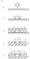
図5は、特開2016−201521号公報に開示されている回路構造体100を示す図である。図5(a)には回路構造体100の平面図が示され、図5(b)には平面図のX−X線に沿った矢視断面図が示される。回路構造体100は、電子部品110と、電子部品110を埋設する樹脂成形体120と、電子部品110の電極111,112にそれぞれ接続された配線140,141とを備える。樹脂成形体120における電子部品110の周囲に溝130が形成される。配線140,141は、溝130内を通過するように液体状の導電インクを塗布して形成される。これにより、樹脂成形体120における配線140,141の下部に膨張が生じても、それに追随して溝130が広がる。このとき、配線140,141に形成された凹部142,143が広がる。これにより配線の断線発生を生じ難くすることができる。 FIG. 5 is a diagram showing a
しかしながら、特開2016−201521号公報に開示されている回路構造体100では、溝130が適正なサイズより大きくなってしまうと、以下の問題が生じる。 However, in the
図6は、適正なサイズよりも大きい溝130が形成された回路構造体100を示す図である。図6(a)には回路構造体の平面図が示され、図6(b)には平面図のX−X線に沿った矢視断面図が示される。溝130が大きくなると、溝130の底面と電子部品110の電極111,112との間の段差が大きくなり、溝130内の配線140aと電極111上の配線140bとが断線する。同様に、溝130内の配線141aと電極112上の配線141bとが断線する。さらに、溝130内の導電インクの流動によって、溝130を通過する配線140a,141aに細線部144,145がそれぞれ生じ、断線が起こりやすくなる。これらの問題は、溝130に供給される導電インクの塗布量を多くすれば解消できるが、大量の導電インクが電子部品110周囲に沿って流れ、配線140,141を短絡させる短絡回路146が形成される可能性がある。 FIG. 6 is a diagram showing the
本発明は、上記の問題点に着目してなされたもので、樹脂成形体に埋設された電子部品に接続する配線の断線が生じ難い電子装置およびその製造方法を提供することを目的としている。 The present invention has been made in view of the above problems, and an object of the present invention is to provide an electronic device in which disconnection of a wiring connected to an electronic component embedded in a resin molded body does not easily occur, and a manufacturing method thereof.
ある局面に従うと、電子装置は、電極を有する電子部品と、電極が露出するように電子部品を埋設する樹脂成形体と、樹脂成形体と電子部品との間に介在し、樹脂成形体から露出する樹脂部材と、樹脂成形体および樹脂部材の上に形成され、電極と接続する配線とを備える。 According to one aspect, an electronic device includes an electronic component having an electrode, a resin molded body in which the electronic component is embedded so that the electrode is exposed, and the electronic component interposed between the resin molded body and the electronic component and exposed from the resin molded body. And a wiring formed on the resin molded body and the resin member and connected to the electrodes.
好ましくは、樹脂部材の熱膨張率は、樹脂成形体の熱膨張率よりも小さく、かつ、電極の熱膨張率よりも大きい。 Preferably, the coefficient of thermal expansion of the resin member is smaller than the coefficient of thermal expansion of the resin molded body and larger than the coefficient of thermal expansion of the electrode.
好ましくは、樹脂部材の曲げ弾性率は、1300MPa以下である。
好ましくは、樹脂部材は、内部に空隙を有する。電子装置は、空隙内に形成され、配線と電極とに接続する導電路をさらに備える。Preferably, the flexural modulus of the resin member is 1300 MPa or less.
Preferably, the resin member has a void inside. The electronic device further includes a conductive path formed in the void and connected to the wiring and the electrode.
別の局面に従うと、上記の電子装置の製造方法は、接着性の液状層が表面に塗布されたシート上に電子部品を配置し、電子部品の側面に沿った液状層の濡れ上がりによって、電子部品の周囲に濡れ上がり部を形成する第1工程と、濡れ上がり部を硬化させて樹脂部材を形成する第2工程と、樹脂部材を形成した後に、シートにおける電子部品の配置面に樹脂材料を射出して、樹脂成形体を成形する第3工程と、樹脂成形体と電子部品との間に樹脂部材が残るように、シートを樹脂成形体から剥離する第4工程と、樹脂成形体および樹脂部材の上に配線を形成する第5工程とを備える。 According to another aspect, the method for manufacturing an electronic device described above, the electronic component is arranged on a sheet having an adhesive liquid layer applied to the surface, and the liquid layer is wetted along the side surface of the electronic component to produce an electronic component. A first step of forming a wetted portion around the component, a second step of curing the wetted portion to form a resin member, and after forming the resin member, apply a resin material to the placement surface of the electronic component on the sheet. A third step of injecting and molding a resin molded body, a fourth step of peeling the sheet from the resin molded body so that the resin member remains between the resin molded body and the electronic component, and the resin molded body and the resin. A fifth step of forming wiring on the member.
好ましくは、液状層は揮発性物質を含み、第2工程において濡れ上がり部を硬化させるときに揮発性物質を揮発させることにより、樹脂部材の内部に空隙を形成する。第5工程において、配線を構成する導電材料を空隙内に浸透させることにより、樹脂部材の内部に配線と電極とに接続する導電路を形成する。 Preferably, the liquid layer contains a volatile substance, and when the wetted portion is cured in the second step, the volatile substance is volatilized to form a void inside the resin member. In the fifth step, a conductive material that forms the wiring is permeated into the voids to form a conductive path that connects the wiring and the electrode inside the resin member.
別の局面に従うと、上記の電子装置の製造方法は、接着性の液状層が表面に塗布されたシート上に電子部品を配置し、電子部品の側面に沿った液状層の濡れ上がりによって、電子部品の周囲に濡れ上がり部を形成する第1工程と、濡れ上がり部を硬化させる第2工程と、シートにおける電子部品の配置面に第1樹脂材料を射出することにより、電子部品を埋設した樹脂成形体を成形する第3工程と、シートおよび濡れ上がり部を樹脂成形体から剥離することにより、樹脂成形体における電子部品の周囲に濡れ上がり部の形状に応じた溝を形成する第4工程と、溝を埋めるように第2樹脂材料を供給し、第2樹脂材料を硬化させて樹脂部材を形成する第5工程と、樹脂成形体および樹脂部材の上に配線を形成する第6工程とを備える。 According to another aspect, the method for manufacturing an electronic device described above, the electronic component is arranged on a sheet having an adhesive liquid layer applied to the surface, and the liquid layer is wetted along the side surface of the electronic component to produce an electronic component. A resin in which the electronic component is embedded by injecting a first resin material onto the surface of the sheet on which the electronic component is arranged, a first step of forming a wetted portion around the component, a second step of curing the wet portion. A third step of molding the molded body, and a fourth step of peeling the sheet and the wetted portion from the resin molded body to form a groove around the electronic component in the resin molded body in accordance with the shape of the wetted portion. A fifth step of supplying a second resin material so as to fill the groove and curing the second resin material to form a resin member, and a sixth step of forming wiring on the resin molded body and the resin member. Prepare
好ましくは、第2樹脂材料は揮発性物質を含み、第5工程において第2樹脂材料を硬化させるときに揮発性物質を揮発させることにより、樹脂部材の内部に空隙を形成する。第6工程において、配線を構成する導電材料を空隙内に浸透させることにより、樹脂部材の内部に配線と電極とに接続する導電路を形成する。 Preferably, the second resin material contains a volatile substance, and when the second resin material is cured in the fifth step, the volatile substance is volatilized to form a void inside the resin member. In the sixth step, the conductive material forming the wiring is infiltrated into the void to form a conductive path connecting the wiring and the electrode inside the resin member.
本開示によれば、樹脂成形体に埋設された電子部品に接続する配線の断線が生じ難い。 According to the present disclosure, disconnection of the wiring connected to the electronic component embedded in the resin molded body is unlikely to occur.
本発明の実施の形態について、図面を参照しながら詳細に説明する。なお、図中の同一または相当部分については、同一符号を付してその説明は繰返さない。また、以下で説明する各実施の形態または変形例は、適宜選択的に組み合わされてもよい。 Embodiments of the present invention will be described in detail with reference to the drawings. It should be noted that the same or corresponding parts in the drawings are designated by the same reference numerals and description thereof will not be repeated. In addition, the respective embodiments or modified examples described below may be selectively combined as appropriate.
<実施の形態1>
(電子装置の構造)
図1は、実施の形態1に係る電子装置1の概略的な構成を示す図である。図1(a)には電子装置1の平面図が示され、図1(b)には平面図のX−X線に沿った矢視断面図が示される。図1には、電子装置1における、1つの電子部品10の周辺を示す一部分が示される。<
(Structure of electronic device)
FIG. 1 is a diagram showing a schematic configuration of the
図1に示されるように、電子装置1は、電子部品10と、樹脂成形体20と、樹脂部材30と、配線40,41とを備えている。 As shown in FIG. 1, the
電子部品10は、受動部品(抵抗、コンデンサ等)、能動部品(LSI、IC等)、電源装置(電池等)、表示装置(LED等)、センサ、スイッチ等から選択される部品である。以下では、電極11,12を有するチップ型の電子部品10を例として説明する。図1には、1つの電子部品10のみが示されているが、電子装置1が備える電子部品10の個数は、1個に限定されず、複数であってもよい。さらに、電子部品10の種類も特に限定されない。The
電子部品10の電極11,12は、たとえば銅(熱膨張率1.7×10⁻⁵/K)または銀(熱膨張率1.9×10−5/K)を主成分とし、ニッケルメッキおよび錫メッキが施されて構成される。The
樹脂成形体20は、板状であり、ポリカーボネイト(PC)(熱膨張率5.6×10⁻⁵/K)またはアクリロニトリルブタジエンスチレン(ABS)(熱膨張率6〜13×10−5/K)等の樹脂からなる。なお、樹脂成形体20の形状は、特に限定されるものではない。樹脂成形体20の材質は、他の種類の樹脂であってもよい。The resin molded
樹脂成形体20は、その上表面21の端部から所定距離(後述する樹脂部材30の幅よりも大きい距離)だけ離れた位置に、電子部品10を埋設して固定する。樹脂成形体20は、上表面21から電極11,12が露出するように電子部品10を埋設する。 The resin molded
樹脂部材30は、電子部品10の周囲に形成され、電子部品10と樹脂成形体20との間に介在する。樹脂部材30は、樹脂成形体20の上表面21から露出する。樹脂部材30の上表面31は、電子部品10における樹脂成形体20から露出した電極11,12の表面と、樹脂成形体20の上表面21と、略同一平面上にある。ここで、上表面31と電極11,12の表面と上表面21とが略同一平面上にあるとは、上表面31と電極11,12の表面との間の段差、および上表面31と上表面21との間の段差が、その上に形成される配線40,41が切断しない程度に所定値より小さいことを意味する。 The
樹脂部材30を構成する樹脂材については特に限定されるものではなく、電子装置1が適用される製品および電子装置1の周囲の環境などに応じて適宜選択された材料によって構成される。たとえば、温度変化が激しい環境下で使用される電子装置1である場合、樹脂部材30は、樹脂成形体20の熱膨張率よりも小さく、かつ、電極11,12の熱膨張率よりも大きい熱膨張率を有する樹脂材で構成されることが好ましい。たとえば、ABSの熱膨張率6〜13×10−5/Kよりも小さく、かつ、電極11,12を構成する銅または銀の熱膨張率1.7〜1.9×10−5/Kよりも大きい熱膨張率3〜5×10−5/Kのエポキシ系、メラミン系の樹脂材により樹脂部材30が構成される。The resin material forming the
あるいは、機械的な負荷を受ける可能性が高い電子装置1である場合、樹脂部材30は、曲げ弾性率20〜1300MPaの弾性を有するエラストマー(たとえば、ポリエステル系、スチレン系、オレフィン系のエラストマー)またはウレタンアクリレート等により構成されることが好ましい。曲げ弾性率は、JIS K7171に従って測定される。 Alternatively, in the case of the
配線40,41は、樹脂成形体20の上表面21および樹脂部材30の上表面31の上に形成され、電子部品10の電極11,12にそれぞれ接続される。配線40は、樹脂部材30の上表面31を通過する形態で電極11に接続され、配線41は、樹脂部材30の上表面31を通過する形態で電極12に接続される。配線40,41の他端は、たとえば電子装置1における図示しない他の電子部品の電極に接続される。これにより、電子部品10は、他の電子部品と電気的かつ機能的に接続される。 The
配線40,41は、たとえばインクジェット印刷法を用いて液状の導電性インク(たとえば、銀(Ag)ナノインク)を噴射することにより、容易に形成することができる。インクジェット印刷法は、液状のインクをノズルから噴射し、インクを噴射対象面上に堆積させる印刷方式である。配線40,41は、Ag以外の材質からなっていてもよいし、他の方法で形成されてもよく、太さおよび厚み等は特に限定されるものではない。 The
(電子装置の製造方法)
図2を参照して、実施の形態1の電子装置1の製造方法について説明する。図2は、実施の形態1の電子装置1の製造方法の一例を説明する図である。(Method of manufacturing electronic device)
A method of manufacturing the
(i)濡れ上がり部形成工程
図2(a)に示されるように、まず、電子部品10を仮固定するためのシート50を用意する。シート50としては、紫外線を透過できる透明性と、後で説明する剥離時の工程を確実にできるようにする柔軟性とを有している材料が好ましく、たとえば、ポリエチレンテレフタレート(PET)、ポリエチレンナフタレート(PEN)、ポリフェニレンサルファイド(PPS)等を用いることができる。本実施形態ではシート50はたとえば50μmの厚さのPETシートである。(I) Wet-up portion forming step As shown in FIG. 2A, first, a
シート50の片面に、接着性の液状層60が塗布されている。液状層60としては、硬化時間が短いものが好ましく、たとえば、紫外線硬化型の接着剤を用いることができる。紫外線硬化型の接着剤は、紫外線が照射されると硬化し、シート50と電子部品10とを接着する。そのため、紫外線を接着剤が塗布されている表面から照射した場合は、電子部品10自身が接着剤に紫外線が照射されるのを阻害する障壁となり、硬化(接着)が不十分となってしまう可能性がある。そのため、シート50に紫外線を透過する材料を用い、シート50の接着剤が塗布されていない表面から紫外線を照射することで、接着剤を十分に硬化させ、電子部品10を短時間で確実にシート50に固定する。本実施形態での液状層60は、たとえば曲げ弾性率47MPaのウレタンアクリレートである。 An
シート50における液状層60が塗布された表面に、電子部品10を位置合わせして配置する。具体的には、電子部品10を、シート50における、樹脂成形体20の上表面21の端部から所定距離だけ離れた位置に対応する位置に配置する。このとき、液状層60は、その表面張力によって電子部品10の側面を濡れ上がる。これにより、電子部品10の周囲に濡れ上がり部61が形成される。 The
濡れ上がり部61の形状(幅および高さ)は、電子部品10の形状、大きさ、材質、および液状層60の材質、表面張力に応じて決まる。液状層60の表面張力を調整すれば、所望の高さの濡れ上がり部61を形成することができる。 The shape (width and height) of the wet-up
(ii)濡れ上がり部硬化工程
濡れ上がり部61の形成後、シート50における電子部品10配置面の反対側の面から1000〜3000mJ/cm2の紫外線を照射する。この結果、液状層60が硬化することによって、電子部品10がシート50に接着固定される。このとき濡れ上がり部61も硬化され、紫外線の照射後もその形状を維持する。濡れ上がり部61は、後の工程を経て電子部品10周辺部の樹脂部材30として使用される。(Ii) Wetting-up portion curing step After forming the wetting-up
(iii)射出成形工程
シート50に電子部品10を仮固定した後、成形型の内部にシート50を配置する。この成形型は、電子部品10が埋設された樹脂成形体20を射出成形するための金型である。シート50における電子部品10が仮固定された面の裏面が、成形型の内面に接するように、シート50を成形型の内部に配置する。この状態で、ABS等の樹脂材料を、成形型温度80℃、射出樹脂温度180℃、かつ射出圧力20kg/cm2の条件で射出する。これにより、図2(c)に示されるように、電子部品10および濡れ上がり部61を埋設した樹脂成形体20が成形される。(Iii) Injection Molding Step After the
(iv)剥離工程
次に図2(d)に示されるように、射出成形工程によって得られた樹脂成形体20からシート50を剥離することによって、樹脂成形体20におけるシート50に対向していた上表面21から電子部品10の電極11,12を露出させる。このとき、仮固定工程において形成された濡れ上がり部61は、シート50から分離し、樹脂成形体20と電子部品10との間に残され、樹脂部材30となる。濡れ上がり部61をシート50から分離するには、電子部品10あるいは樹脂成形体20の材料と接着特性の良好な材料を液状層60として選択することで容易に実現可能である。この結果、電子部品10と電子部品10の周囲に配置された樹脂部材30とを埋設した樹脂成形体20が形成される。(Iv) Peeling Step Next, as shown in FIG. 2D, the
(v)配線形成工程
最後に図2(e)に示されるように、樹脂成形体20の表面から露出する電極11,12と接続する配線40,41を、樹脂成形体20の上表面21および樹脂部材30の上表面31の上に形成する。たとえば、配線40,41の材料である液状の導電性インク(たとえば、銀ナノインク)を噴射する方法(たとえばインクジェット印刷法)を用いて配線40,41が形成される。このとき、インクジェットヘッドの噴出口が樹脂部材30上を通過するようにインクジェットヘッドを移動する。これにより、配線40,41は、樹脂部材30を通過するように形成される。より詳細には、配線40,41は、樹脂成形体20における上表面21および樹脂部材30における上表面31を連続的に覆うように形成される。本工程により、電子部品10が樹脂成形体20に埋設された電子装置1が完成する。(V) Wiring forming step Finally, as shown in FIG. 2E, the
配線40,41は、インクジェット印刷法の代わりに、スクリーン印刷法またはディスペンサによる方法を用いて形成されてもよい。さらに、電子装置1において、配線40,41を覆うレジスト層が形成されてもよい。 The
(利点)
以上のように、本実施の形態1の電子装置1は、電極11,12を有する電子部品10と、電極11,12が露出するように電子部品10を埋設する樹脂成形体20と、樹脂成形体20と電子部品10との間に介在し、樹脂成形体20から露出する樹脂部材30と、樹脂成形体20および樹脂部材30の上に形成され、電極11,12とそれぞれ接続する配線40,41とを備える。(advantage)
As described above, the
上記の構成によれば、配線40,41は、樹脂部材30を通過して電極11,12に接続する。樹脂部材30が存在することにより、樹脂成形体20と電子部品10との間に大きな溝が形成されている場合と比較して、配線40,41の断線を抑制することができる。 According to the above configuration, the
樹脂部材30の熱膨張率は、樹脂成形体20の熱膨張率よりも小さく、かつ、電極11,12の熱膨張率よりも大きいことが好ましい。これにより、電子装置1の周囲の温度変化によって樹脂成形体20に膨張または収縮の形状変化が生じたとしても、樹脂成形体20と電子部品10との間に介在する樹脂部材30によって、配線40,41にかかる応力が分散される。その結果、配線40,41の断線の発生を生じ難くすることができる。 The coefficient of thermal expansion of the
樹脂部材30の曲げ弾性率は、1300MPa以下であることが好ましい。曲げ弾性率が1300MPa以下であることにより、樹脂成形体20と電子部品10との間を広げるような機械的負荷が電子装置1に加わった場合であっても、樹脂部材30が樹脂成形体20に追従して伸び、配線40,41にかかる応力が分散される。その結果、配線40,41の断線の発生を生じ難くすることができる。さらに、樹脂部材30の曲げ弾性率は、20MPa以上であることが好ましい。曲げ弾性率が20MPa未満であると樹脂部材30の硬度(硬さ)が小さくなりすぎて、表面に形成される配線40,41にクラック等の欠陥が生じやすくなる。しかしながら、樹脂部材30の曲げ弾性率を20MPa以上とすることにより、このような欠陥の発生を抑制することができる。 The bending elastic modulus of the
本実施の形態1の電子装置1の製造方法は、濡れ上がり部形成工程(第1工程)と、濡れ上がり部硬化工程(第2工程)と、射出成形工程(第3工程)と、剥離工程(第4工程)と、配線形成工程(第5工程)とを備える。濡れ上がり部形成工程では、接着性の液状層60が表面に塗布されたシート50上に電極11,12を有する電子部品10を配置し、電子部品10の側面に沿った液状層60の濡れ上がりによって、電子部品10の周囲に濡れ上がり部61を形成する。濡れ上がり部硬化工程では、濡れ上がり部61を硬化させて樹脂部材30を形成する。射出成形工程では、樹脂部材30を形成した後に、シート50における電子部品10の配置面に樹脂材料を射出して、電子部品10を埋設した樹脂成形体20を成形する。剥離工程では、樹脂成形体20と電子部品10との間に樹脂部材30が残るように、シート50を樹脂成形体20から剥離する。配線形成工程では、樹脂成形体20および樹脂部材30の上に、電極11,12とそれぞれ接続する配線40,41を形成する。 The method of manufacturing the
上記の構成によれば、樹脂成形体20と電子部品10との間に樹脂部材30が介在した電子装置1が容易に製造される。配線40,41は、樹脂部材30を通過して電極11,12に接続する。樹脂部材30が存在することにより、樹脂成形体20と電子部品10との間に大きな溝が形成されている場合と比較して、配線40,41の断線を抑制することができる。 According to the above configuration, the
<実施の形態2>
実施の形態2に係る電子装置について以下に説明する。図3は、実施の形態2に係る電子装置1aを示す断面図である。図3に示されるように、電子装置1aは、樹脂部材30の代わりに樹脂部材32を備えるとともに、樹脂部材32の内部の空隙内に形成された多数の導電路42,43を備える点で、実施の形態1の電子装置1と相違する。<Second Embodiment>
The electronic device according to the second embodiment will be described below. FIG. 3 is a cross-sectional view showing the
樹脂部材32は、内部に多数の空隙を有する多孔質の樹脂体である。空隙には、樹脂部材32内の孔および亀裂が含まれる。樹脂部材32の形成方法は、実施の形態1における樹脂部材30の形成方法(図2(a)〜図2(c)参照)と同様である。ただし、シート50に塗布される液状層として、揮発性液体を含む接着性の材料を用い、液状層を光硬化させる際に熱処理を行なって、揮発性液体を揮発させる。揮発性液体としては、当該熱処理によって揮発する液体(たとえば、ビニルエーテルなど)が用いられる。 The
液状層としては、たとえば、エポキシ樹脂30質量%、ビニルエーテル化合物50質量%、イオン液体10質量%、残部10質量%になるように配合されたインク材を用いる。残部には、光カチオン重合開始剤および安定化剤などが含まれる。 As the liquid layer, for example, an ink material is used which is mixed so that the epoxy resin is 30% by mass, the vinyl ether compound is 50% by mass, the ionic liquid is 10% by mass, and the balance is 10% by mass. The balance contains a photocationic polymerization initiator and a stabilizer.
イオン液体は、陰イオンと陽イオンとからなり、常温(たとえば25℃)で液体である非高分子物質である。陽イオンとしては、イミダゾリウムイオンなどの環状アミジンイオン、ピリジニウムイオン、アンモニウムイオン、スルホニウムイオン、ホスホニウムイオン等が挙げられる。陰イオンとしては、CnH2n+1COO−、CnF2n+1COO−、NO3−、CnF2n+1SO3−、(CnF2n+1SO2)2N−、(CnF2n+1SO2)3C−、PO42−、AlCl4−、Al2Cl7−、ClO4−、BF4−、PF6−、AsF6−、SbF6−等が挙げられる。The ionic liquid is a non-polymeric substance composed of anions and cations and is a liquid at room temperature (for example, 25 ° C.). Examples of the cation include cyclic amidine ion such as imidazolium ion, pyridinium ion, ammonium ion, sulfonium ion, phosphonium ion and the like. Theanion, C n H 2n + 1 COO -, C n F 2n + 1 COO -, NO 3 -, C n F 2n + 1 SO 3 -, (C n F 2n + 1 SO 2) 2 N -, (C n F 2n + 1 SO 2 )3 C− , PO42− , AlCl4− , Al2 Cl7− , ClO4− , BF4− , PF6− , AsF6− , SbF6− and the like.
光カチオン重合開始剤としては、公知の材料を使用することができ、たとえば、スルホニウム塩(スルホニウムイオンとアニオンとの塩)、ヨードニウム塩(ヨードニウムイオンとアニオンとの塩)、セレニウム塩(セレニウムイオンとアニオンとの塩)、アンモニウム塩(アンモニウムイオンとアニオンとの塩)、ホスホニウム塩(ホスホニウムイオンとアニオンとの塩)、遷移金属錯体イオンとアニオンとの塩等を用いることができる。 As the photocationic polymerization initiator, known materials can be used, for example, sulfonium salt (salt of sulfonium ion and anion), iodonium salt (salt of iodonium ion and anion), selenium salt (selenium ion and Anion salt), ammonium salt (ammonium ion and anion salt), phosphonium salt (phosphonium ion and anion salt), transition metal complex ion and anion salt and the like can be used.
上記の液状層を光硬化させ、かつ、熱処理する際に、内部の揮発性液体(ビニルエーテル化合物)が揮発し、当該揮発性液体の体積に相当する孔、あるいは、体積収縮による多数の亀裂が濡れ上がり部61に生じ、多数の空隙を有する樹脂部材32が形成される。 When the above liquid layer is photo-cured and heat-treated, the volatile liquid (vinyl ether compound) inside volatilizes, and the pores corresponding to the volume of the volatile liquid or many cracks due to volume contraction get wet. The
導電路42,43は、樹脂部材32内の空隙内に形成される。導電路42は、配線40と電極11とに接続される。導電路43は、配線41と電極12とに接続される。 The
導電路42,43は、配線40,41と同時に形成される。具体的には、実施の形態1の(v)配線形成工程と同様の工程において、樹脂部材32上に液状の導電性インクを噴射して、配線40,41を形成する。このとき、毛細管現象によって導電性インクの一部が樹脂部材32内の空隙に浸透し、電極11または電極12に到達する。これにより、樹脂部材32の空隙内に、配線40と電極11とに接続された導電路42と、配線41と電極12とに接続された導電路43とが形成される。 The
導電性インクの一部は、網目状に形成された樹脂部材32内の空隙に浸透する。そのため、配線40と電極11とは多数の経路によって接続される。当該多数の経路の各々が導電路42を構成する。よって、配線40と電極11とに間には多数の導電路42が形成される。同様に、配線41と電極12とに間には多数の導電路43が形成される。 A part of the conductive ink penetrates into the voids in the
配線40,41における樹脂部材32上の部分には、樹脂部材32に浸透した導電性インクの体積に相当する凹部44,45が形成される。凹部44,45による抵抗上昇の影響が許容できない場合には、樹脂部材32上への導電性インクの供給量を適宜増加すればよい。
樹脂成形体20に何らかの原因(熱衝撃、周囲温度の変化、機械的負荷等)によって膨張または収縮の形状変化が生じ、配線40,41に亀裂が発生する可能性がある。このとき、樹脂部材32の一部にまで亀裂が進行したとしても、樹脂部材32内の多数の導電路42,43のうち、亀裂が生じていない部分を通る導電路42,43によって、配線40,41と電極11,12との間のそれぞれの電気的接続が維持される。これにより、配線40,41と電極11,12とのそれぞれの接続信頼性を向上させることができる。 There is a possibility that the resin molded
<実施の形態3>
上記の実施の形態1では、濡れ上がり部61を樹脂成形体20側に残すようにシート50を樹脂成形体20から剥離することにより、電子部品10と樹脂成形体20との間に介在する樹脂部材30を形成した。これに対し、本実施の形態3では、濡れ上がり部61とともにシート50を樹脂成形体20から剥離することにより形成された電子部品10の周囲の溝を埋めるように樹脂部材30を形成する。本実施の形態3に係る電子装置は、実施の形態1に係る電子装置1と同様の構成を有する。<Third Embodiment>
In the above-described first embodiment, the
図2および図4を参照して、実施の形態3に係る電子装置の製造方法について説明する。図4は、実施の形態3に係る電子装置の製造方法を説明するための図である。 A method of manufacturing the electronic device according to the third embodiment will be described with reference to FIGS. 2 and 4. FIG. 4 is a diagram for explaining the method of manufacturing the electronic device according to the third embodiment.
まず、図2(a)〜図2(c)に示されるように、実施の形態1の(i)濡れ上がり部形成工程〜(iii)射出成形工程を行なうことにより、電子部品10および濡れ上がり部61を埋設した樹脂成形体20が成形される。ただし、濡れ上がり部61を構成する接着性の液状層60の材料として、シート50との接着力が実施の形態1の材料よりも強く、かつ、樹脂成形体20との接着力が実施の形態1の材料よりも弱い材料が選択される。 First, as shown in FIGS. 2 (a) to 2 (c), the
(iv)剥離工程
次に、射出成形工程によって得られた樹脂成形体20からシート50を剥離することによって、樹脂成形体20におけるシート50に対向していた上表面21から電子部品10の電極11,12を露出させる。このとき、図4(a)に示されるように、仮固定工程において形成された濡れ上がり部61は、シート50とともに、樹脂成形体20から剥離する。これにより、樹脂成形体20における電子部品10の周囲に、濡れ上がり部61の形状に応じた溝70が形成される。(Iv) Peeling Step Next, by peeling the
(v)樹脂部材形成工程
次に、電子部品10の周囲の溝70を埋めるように樹脂材を供給して、溝70の形状に沿った樹脂部材30を形成する。樹脂部材30の樹脂材料としては、実施の形態1の液状層60の材料を用いることができる。樹脂材は、実施の形態1の(v)配線形成工程と同様にインクジェット印刷法を用いて溝70に供給され、紫外線照射または熱処理によって硬化される。(V) Resin Member Forming Step Next, a resin material is supplied so as to fill the
樹脂部材30は、溝70からはみ出して形成されてもよいが、電極11,12の全体を覆うことがないように形成される。 The
最後に、樹脂成形体20の表面から露出する電極11,12と接続する配線40,41を、樹脂成形体20の上表面21および樹脂部材30の上に形成する。この工程は、実施の形態1の(v)配線形成工程と同様であるため、詳細な説明を省略する。 Finally, the
以上のように、本実施の形態3の電子装置の製造方法は、実施の形態1の(i)濡れ上がり部形成工程〜(iii)射出成形工程および(v)配線形成工程に加えて、剥離工程と、樹脂部材形成工程とを備える。剥離工程では、シート50および濡れ上がり部61を樹脂成形体20から剥離することにより、樹脂成形体20における電子部品10の周囲に濡れ上がり部61の形状に応じた溝70を形成する。樹脂部材形成工程では、溝70を埋めるように樹脂部材30を形成する。これにより、樹脂成形体20と電子部品10との間に樹脂部材30が介在し、樹脂部材30を通過するように形成された配線40,41を備える電子装置を容易に製造することができる。 As described above, the electronic device manufacturing method according to the third embodiment includes peeling in addition to the steps (i) wetted portion forming step to (iii) injection molding step and (v) wiring forming step of the first embodiment. And a resin member forming step. In the peeling step, the
樹脂部材形成工程において、電子部品10の周囲の溝70に供給される樹脂材料として、実施の形態2の液状層と同様に、揮発性物質を含む材料を用いてもよい。これにより、実施の形態2と同様に、内部に空隙を有する樹脂部材32を形成することができる。その後、配線形成工程において、配線40,41を構成する導電材料を空隙内に浸透させることにより、樹脂部材32の内部に、配線40と電極11とに接続する導電路42と、配線41と電極12とに接続する導電路43とを形成することができる。 In the resin member forming step, as the resin material supplied to the
今回開示された実施の形態はすべての点で例示であって制限的なものではないと考えられるべきである。本発明の範囲は、上記した説明ではなく、特許請求の範囲によって示され、特許請求の範囲と均等の意味および範囲内でのすべての変更が含まれることが意図される。 The embodiments disclosed this time are to be considered as illustrative in all points and not restrictive. The scope of the present invention is shown not by the above description but by the claims, and is intended to include meanings equivalent to the claims and all modifications within the scope.
1,1a 電子装置、10,110 電子部品、11,12,111,112 電極、20,120 樹脂成形体、21,31 上表面、30,32 樹脂部材、40,41,140,140a,140b,141,141a,141b 配線、42,43 導電路、44,45,142,143 凹部、50 シート、60 液状層、61 濡れ上がり部、70,130 溝、100 回路構造体、144,145 細線部、146 短絡回路。 1,1a electronic device, 10,110 electronic component, 11,12,111,112 electrode, 20,120 resin molded body, 21,31 upper surface, 30,32 resin member, 40,41,140,140a, 140b, 141, 141a, 141b Wiring, 42, 43 Conductive path, 44, 45, 142, 143 Recessed part, 50 sheet, 60 Liquid layer, 61 Wetting part, 70, 130 groove, 100 Circuit structure, 144, 145 Fine line part, 146 short circuit.
Claims (6)
Translated fromJapanese前記電極が露出するように前記電子部品を埋設する樹脂成形体と、
前記樹脂成形体と前記電子部品との間に介在し、前記樹脂成形体から露出する樹脂部材と、
前記樹脂成形体および前記樹脂部材の上に形成され、前記電極と接続する配線とを備え、
前記樹脂部材の熱膨張率は、前記樹脂成形体の熱膨張率よりも小さく、かつ、前記電極の熱膨張率よりも大きい、電子装置。An electronic component having an electrode,
A resin molded body in which the electronic component is embedded so that the electrodes are exposed;
A resin member interposed between the resin molded body and the electronic component and exposed from the resin molded body,
Wherein formed on the resin molded body and the resin member,e Bei wiring and for connecting with saidelectrode,
An electronic device in which thecoefficient of thermal expansion of the resin member is smaller than the coefficient of thermal expansion of the resin molded body and is larger than the coefficient of thermal expansion of the electrode .
前記電極が露出するように前記電子部品を埋設する樹脂成形体と、
前記樹脂成形体と前記電子部品との間に介在し、前記樹脂成形体から露出する樹脂部材と、
前記樹脂成形体および前記樹脂部材の上に形成され、前記電極と接続する配線とを備える電子装置であって、
前記樹脂部材は、内部に空隙を有し、
前記電子装置は、前記空隙内に形成され、前記配線と前記電極とに接続する導電路をさらに備える、電子装置。An electronic component having an electrode,
A resin molded body in which the electronic component is embedded so that the electrodes are exposed;
A resin member interposed between the resin molded body and the electronic component and exposed from the resin molded body,
An electronic device provided on the resin molded body and the resin member, comprising: a wiring connected to the electrode,
The resin member has a void inside,
The electronic device is formed in the gap, further comprising a conductive path for connecting the wiring to saidelectrode, electronic device.
前記電極が露出するように前記電子部品を埋設する樹脂成形体と、
前記樹脂成形体と前記電子部品との間に介在し、前記樹脂成形体から露出する樹脂部材と、
前記樹脂成形体および前記樹脂部材の上に形成され、前記電極と接続する配線とを備える電子装置の製造方法であって、
接着性の液状層が表面に塗布されたシート上に前記電子部品を配置し、前記電子部品の側面に沿った前記液状層の濡れ上がりによって、前記電子部品の周囲に濡れ上がり部を形成する第1工程と、
前記濡れ上がり部を硬化させて前記樹脂部材を形成する第2工程と、
前記樹脂部材を形成した後に、前記シートにおける前記電子部品の配置面に樹脂材料を射出して、前記樹脂成形体を成形する第3工程と、
前記樹脂成形体と前記電子部品との間に前記樹脂部材が残るように、前記シートを前記樹脂成形体から剥離する第4工程と、
前記樹脂成形体および前記樹脂部材の上に前記配線を形成する第5工程とを備える、電子装置の製造方法。An electronic component having an electrode,
A resin molded body in which the electronic component is embedded so that the electrodes are exposed;
A resin member interposed between the resin molded body and the electronic component and exposed from the resin molded body,
A method of manufacturing an electronic device,comprising: a resin molded body and a wiring formed on the resin member, the wiring connecting to the electrodes ,
Arranging the electronic component on a sheet coated with an adhesive liquid layer on the surface, by the wetting of the liquid layer along the side surface of the electronic component, to form a wet portion around the electronic component 1 step,
A second step of curing the wet-up portion to form the resin member;
A third step of molding the resin molded body by injecting a resin material onto the surface of the sheet on which the electronic component is arranged after forming the resin member,
A fourth step of peeling the sheet from the resin molded body so that the resin member remains between the resin molded body and the electronic component;
And a fifth step of forming the wiring on the resin molded body and the resin member.
前記第2工程において前記濡れ上がり部を硬化させるときに前記揮発性物質を揮発させることにより、前記樹脂部材の内部に空隙を形成し、
前記第5工程において、前記配線を構成する導電材料を前記空隙内に浸透させることにより、前記樹脂部材の内部に前記配線と前記電極とに接続する導電路を形成する、請求項3に記載の電子装置の製造方法。The liquid layer contains a volatile substance,
Forming voids inside the resin member by volatilizing the volatile substance when curing the wet-up portion in the second step,
In the fifth step, by impregnating a conductive material constituting the wiring inside the gap, to form a conductive path to be connected to said said wire electrode in the interior of the resin member, as claimed in claim3 Electronic device manufacturing method.
前記電極が露出するように前記電子部品を埋設する樹脂成形体と、
前記樹脂成形体と前記電子部品との間に介在し、前記樹脂成形体から露出する樹脂部材と、
前記樹脂成形体および前記樹脂部材の上に形成され、前記電極と接続する配線とを備える電子装置の製造方法であって、
接着性の液状層が表面に塗布されたシート上に前記電子部品を配置し、前記電子部品の側面に沿った前記液状層の濡れ上がりによって、前記電子部品の周囲に濡れ上がり部を形成する第1工程と、
前記濡れ上がり部を硬化させる第2工程と、
前記シートにおける前記電子部品の配置面に第1樹脂材料を射出することにより、前記電子部品を埋設した樹脂成形体を成形する第3工程と、
前記シートおよび前記濡れ上がり部を前記樹脂成形体から剥離することにより、前記樹脂成形体における前記電子部品の周囲に前記濡れ上がり部の形状に応じた溝を形成する第4工程と、
前記溝を埋めるように第2樹脂材料を供給し、前記第2樹脂材料を硬化させて前記樹脂部材を形成する第5工程と、
前記樹脂成形体および前記樹脂部材の上に前記配線を形成する第6工程とを備える、電子装置の製造方法。An electronic component having an electrode,
A resin molded body in which the electronic component is embedded so that the electrodes are exposed;
A resin member interposed between the resin molded body and the electronic component and exposed from the resin molded body,
A method of manufacturing an electronic device,comprising: a resin molded body and a wiring formed on the resin member, the wiring connecting to the electrodes ,
Arranging the electronic component on a sheet coated with an adhesive liquid layer on the surface, by wetting of the liquid layer along the side surface of the electronic component, to form a wet portion around the electronic component 1 step,
A second step of curing the wet-up portion,
A third step of molding a resin molded body in which the electronic component is embedded by injecting a first resin material onto a surface of the sheet on which the electronic component is arranged;
A fourth step of forming a groove corresponding to the shape of the wetting portion around the electronic component in the resin molding by peeling the sheet and the wetting portion from the resin molding,
A fifth step of supplying a second resin material so as to fill the groove and curing the second resin material to form the resin member;
And a sixth step of forming the wiring on the resin molded body and the resin member.
前記第5工程において前記第2樹脂材料を硬化させるときに前記揮発性物質を揮発させることにより、前記樹脂部材の内部に空隙を形成し、
前記第6工程において、前記配線を構成する導電材料を前記空隙内に浸透させることにより、前記樹脂部材の内部に前記配線と前記電極とに接続する導電路を形成する、請求項5に記載の電子装置の製造方法。The second resin material includes a volatile substance,
In the fifth step, when the second resin material is cured, the volatile substance is volatilized to form a void inside the resin member,
In the sixth step, by impregnating a conductive material constituting the wiring inside the gap, to form a conductive path to be connected to said said wire electrode in the interior of the resin member, according to claim5 Electronic device manufacturing method.
Priority Applications (6)
| Application Number | Priority Date | Filing Date | Title |
|---|---|---|---|
| JP2017034684AJP6693441B2 (en) | 2017-02-27 | 2017-02-27 | Electronic device and manufacturing method thereof |
| US16/464,704US10618206B2 (en) | 2017-02-27 | 2017-11-16 | Resin-molded electronic device with disconnect prevention |
| EP17897410.1AEP3589089B1 (en) | 2017-02-27 | 2017-11-16 | Electronic device and method for manufacturing same |
| CN201780072787.4ACN110024493B (en) | 2017-02-27 | 2017-11-16 | Electronic device and method for manufacturing the same |
| PCT/JP2017/041269WO2018154879A1 (en) | 2017-02-27 | 2017-11-16 | Electronic device and method for manufacturing same |
| TW106141187ATWI657723B (en) | 2017-02-27 | 2017-11-27 | Electronic device and manufacturing method thereof |
Applications Claiming Priority (1)
| Application Number | Priority Date | Filing Date | Title |
|---|---|---|---|
| JP2017034684AJP6693441B2 (en) | 2017-02-27 | 2017-02-27 | Electronic device and manufacturing method thereof |
Publications (3)
| Publication Number | Publication Date |
|---|---|
| JP2018142573A JP2018142573A (en) | 2018-09-13 |
| JP2018142573A5 JP2018142573A5 (en) | 2019-04-11 |
| JP6693441B2true JP6693441B2 (en) | 2020-05-13 |
Family
ID=63254260
Family Applications (1)
| Application Number | Title | Priority Date | Filing Date |
|---|---|---|---|
| JP2017034684AExpired - Fee RelatedJP6693441B2 (en) | 2017-02-27 | 2017-02-27 | Electronic device and manufacturing method thereof |
Country Status (6)
| Country | Link |
|---|---|
| US (1) | US10618206B2 (en) |
| EP (1) | EP3589089B1 (en) |
| JP (1) | JP6693441B2 (en) |
| CN (1) | CN110024493B (en) |
| TW (1) | TWI657723B (en) |
| WO (1) | WO2018154879A1 (en) |
Family Cites Families (50)
| Publication number | Priority date | Publication date | Assignee | Title |
|---|---|---|---|---|
| GB2133499B (en)* | 1982-11-16 | 1985-10-09 | Honda Motor Co Ltd | Shafts incorporating fibre-reinforced plastics |
| JPS60257546A (en)* | 1984-06-04 | 1985-12-19 | Mitsubishi Electric Corp | Semiconductor device and its manufacturing method |
| JPH0752762B2 (en)* | 1985-01-07 | 1995-06-05 | 株式会社日立製作所 | Semiconductor resin package |
| JPS6331149A (en)* | 1986-07-25 | 1988-02-09 | Fujitsu Ltd | semiconductor equipment |
| US4993895A (en)* | 1990-01-08 | 1991-02-19 | Edward Nordstrom | Apparatus for retaining a tile in a secure position to prevent rotation while an opening is drilled through the tile |
| JP2794262B2 (en) | 1993-08-30 | 1998-09-03 | 国際電気株式会社 | Electronic circuit package |
| JP2973792B2 (en)* | 1993-09-21 | 1999-11-08 | 富士電機株式会社 | Resin-sealed semiconductor device |
| JP2848357B2 (en)* | 1996-10-02 | 1999-01-20 | 日本電気株式会社 | Semiconductor device mounting method and its mounting structure |
| JP3509507B2 (en)* | 1997-11-10 | 2004-03-22 | 松下電器産業株式会社 | Mounting structure and mounting method of electronic component with bump |
| JP2000012744A (en)* | 1998-06-19 | 2000-01-14 | Fujitsu Ltd | Semiconductor device and manufacturing method thereof |
| US6258191B1 (en)* | 1998-09-16 | 2001-07-10 | International Business Machines Corporation | Method and materials for increasing the strength of crystalline ceramic |
| JP3844936B2 (en)* | 1999-03-26 | 2006-11-15 | 富士通株式会社 | Semiconductor device |
| US6481819B2 (en)* | 2000-07-10 | 2002-11-19 | Canon Kabushiki Kaisha | Ink jet recording head and recording apparatus having recording element substrates with different liquid ejection systems |
| JP2002151551A (en)* | 2000-11-10 | 2002-05-24 | Hitachi Ltd | Flip-chip mounting structure, semiconductor device therewith and mounting method |
| JP2002170853A (en)* | 2000-12-01 | 2002-06-14 | Nec Corp | Flip chip mounting method |
| JP4248157B2 (en)* | 2000-12-15 | 2009-04-02 | イビデン株式会社 | Multilayer printed wiring board |
| US6835592B2 (en)* | 2002-05-24 | 2004-12-28 | Micron Technology, Inc. | Methods for molding a semiconductor die package with enhanced thermal conductivity |
| JP2003347741A (en)* | 2002-05-30 | 2003-12-05 | Taiyo Yuden Co Ltd | Composite multilayer substrate and module using the same |
| JP3906767B2 (en)* | 2002-09-03 | 2007-04-18 | 株式会社日立製作所 | Electronic control unit for automobile |
| JP2004111502A (en) | 2002-09-17 | 2004-04-08 | Matsushita Electric Ind Co Ltd | Exterior parts and portable electronic devices |
| JP2005064479A (en)* | 2003-07-31 | 2005-03-10 | Sanyo Electric Co Ltd | Circuit module |
| JP2005056916A (en)* | 2003-08-05 | 2005-03-03 | Toyota Industries Corp | Circuit board |
| KR100510556B1 (en)* | 2003-11-11 | 2005-08-26 | 삼성전자주식회사 | Semiconductor package having ultra thin thickness and method for manufacturing the same |
| JP2006100752A (en)* | 2004-09-30 | 2006-04-13 | Sanyo Electric Co Ltd | Circuit arrangement and its manufacturing method |
| JP2006165252A (en)* | 2004-12-07 | 2006-06-22 | Shinko Electric Ind Co Ltd | Method of manufacturing substrate with built-in chip |
| US7442581B2 (en)* | 2004-12-10 | 2008-10-28 | Freescale Semiconductor, Inc. | Flexible carrier and release method for high volume electronic package fabrication |
| JP5164362B2 (en) | 2005-11-02 | 2013-03-21 | キヤノン株式会社 | Semiconductor embedded substrate and manufacturing method thereof |
| US7426117B2 (en)* | 2005-12-21 | 2008-09-16 | Xerox Corporation | Chip on a board |
| TWI325644B (en)* | 2007-01-03 | 2010-06-01 | Chipmos Technologies Inc | Chip package and manufacturing thereof |
| JP5543086B2 (en)* | 2008-06-25 | 2014-07-09 | ピーエスフォー ルクスコ エスエイアールエル | Semiconductor device and manufacturing method thereof |
| DE102008054104A1 (en)* | 2008-10-31 | 2010-05-06 | Herbert Kannegiesser Gmbh | Method and device for treating the exhaust air from heated laundry machines |
| JP2010114221A (en) | 2008-11-05 | 2010-05-20 | Seiko Epson Corp | Electronic apparatus, and method of manufacturing the same |
| US8525041B2 (en)* | 2009-02-20 | 2013-09-03 | Ibiden Co., Ltd. | Multilayer wiring board and method for manufacturing the same |
| JP5359550B2 (en) | 2009-05-22 | 2013-12-04 | オムロン株式会社 | Manufacturing method of electronic component mounting apparatus |
| JP5582597B2 (en)* | 2009-09-30 | 2014-09-03 | セイコーインスツル株式会社 | Electronic circuit components and electronic equipment |
| JP5250524B2 (en)* | 2009-10-14 | 2013-07-31 | ルネサスエレクトロニクス株式会社 | Semiconductor device and manufacturing method thereof |
| DE102009058764A1 (en)* | 2009-12-15 | 2011-06-16 | Fraunhofer-Gesellschaft zur Förderung der angewandten Forschung e.V. | Method for producing an electronic assembly and electronic assembly |
| JP2012094592A (en)* | 2010-10-25 | 2012-05-17 | Elpida Memory Inc | Semiconductor device and method of manufacturing the same |
| DE112011103926B4 (en)* | 2010-11-25 | 2018-03-08 | Mitsubishi Electric Corporation | Semiconductor device |
| US8735739B2 (en)* | 2011-01-13 | 2014-05-27 | Ibiden Co., Ltd. | Wiring board and method for manufacturing the same |
| JP2012204831A (en)* | 2011-03-23 | 2012-10-22 | Ibiden Co Ltd | Electronic component built-in wiring board and manufacturing method of the same |
| JP5441956B2 (en)* | 2011-05-26 | 2014-03-12 | 三菱電機株式会社 | Resin-sealed electronic control device and manufacturing method thereof |
| JP5853106B2 (en)* | 2012-11-09 | 2016-02-09 | 株式会社日立製作所 | Junction structure and manufacturing method thereof |
| JP2014107431A (en)* | 2012-11-28 | 2014-06-09 | Ibiden Co Ltd | Electronic component built-in wiring board, and manufacturing method for electronic component built-in wiring board |
| JP6334962B2 (en)* | 2014-03-05 | 2018-05-30 | 新光電気工業株式会社 | WIRING BOARD AND WIRING BOARD MANUFACTURING METHOD |
| JP6354285B2 (en)* | 2014-04-22 | 2018-07-11 | オムロン株式会社 | Resin structure in which electronic component is embedded and method for manufacturing the same |
| JP6500572B2 (en)* | 2015-04-14 | 2019-04-17 | オムロン株式会社 | Circuit structure |
| KR102494332B1 (en)* | 2015-07-15 | 2023-02-02 | 삼성전기주식회사 | Electronic Component Package |
| JP6711098B2 (en)* | 2016-04-15 | 2020-06-17 | オムロン株式会社 | Heat dissipation structure of semiconductor device |
| JP6648626B2 (en)* | 2016-04-27 | 2020-02-14 | オムロン株式会社 | Electronic device and method of manufacturing the same |
- 2017
- 2017-02-27JPJP2017034684Apatent/JP6693441B2/ennot_activeExpired - Fee Related
- 2017-11-16USUS16/464,704patent/US10618206B2/ennot_activeExpired - Fee Related
- 2017-11-16CNCN201780072787.4Apatent/CN110024493B/ennot_activeExpired - Fee Related
- 2017-11-16WOPCT/JP2017/041269patent/WO2018154879A1/ennot_activeCeased
- 2017-11-16EPEP17897410.1Apatent/EP3589089B1/ennot_activeNot-in-force
- 2017-11-27TWTW106141187Apatent/TWI657723B/ennot_activeIP Right Cessation
Also Published As
| Publication number | Publication date |
|---|---|
| CN110024493A (en) | 2019-07-16 |
| EP3589089A1 (en) | 2020-01-01 |
| US20190322015A1 (en) | 2019-10-24 |
| EP3589089B1 (en) | 2022-03-09 |
| JP2018142573A (en) | 2018-09-13 |
| TWI657723B (en) | 2019-04-21 |
| TW201832626A (en) | 2018-09-01 |
| EP3589089A4 (en) | 2020-12-30 |
| CN110024493B (en) | 2022-02-18 |
| US10618206B2 (en) | 2020-04-14 |
| WO2018154879A1 (en) | 2018-08-30 |
Similar Documents
| Publication | Publication Date | Title |
|---|---|---|
| JP5093353B2 (en) | Manufacturing method of component built-in module and component built-in module | |
| CN106257965B (en) | Flexible Printed Circuit Board | |
| JP2007165888A (en) | Printed-circuit substrate in which electron devices are built, and its manufacturing method | |
| KR20090130727A (en) | Electronic component embedded printed circuit board and manufacturing method | |
| JP4158714B2 (en) | Method for manufacturing electronic component mounted substrate | |
| JP5454681B2 (en) | Module substrate and manufacturing method thereof | |
| JP6693441B2 (en) | Electronic device and manufacturing method thereof | |
| TWI677266B (en) | Circuit structure and production method thereof | |
| KR20120130639A (en) | Double layer fpcb and manufacting method thereof | |
| WO2019026319A1 (en) | Electronic device and manufacturing method thereof | |
| KR20130033851A (en) | Multi layer pcb and manufacturing method thereof | |
| KR20130046716A (en) | The printed circuit board and the method for manufacturing the same | |
| JP6658935B2 (en) | Circuit structure | |
| WO2020188955A1 (en) | Electronic module, electronic device, and manufacturing methods therefor | |
| JP5561683B2 (en) | Component built-in board | |
| KR20140076090A (en) | Printed circuit board and manufacturing method thereof | |
| KR20090060551A (en) | Method for manufacturing printed circuit board embedded semiconductor device | |
| JP2008282953A (en) | Wiring board manufacturing method | |
| JP2009192997A (en) | Display panel, display panel manufacturing method, and display panel device | |
| KR20130076497A (en) | Printed circuit board including metal pattern including a seed layer and a plating layer, and method for manufacturing the same | |
| KR20110018683A (en) | Embedded Circuit Boards and Methods of Manufacturing Embedded Circuit Boards |
Legal Events
| Date | Code | Title | Description |
|---|---|---|---|
| A521 | Request for written amendment filed | Free format text:JAPANESE INTERMEDIATE CODE: A523 Effective date:20190228 | |
| A621 | Written request for application examination | Free format text:JAPANESE INTERMEDIATE CODE: A621 Effective date:20190228 | |
| TRDD | Decision of grant or rejection written | ||
| A01 | Written decision to grant a patent or to grant a registration (utility model) | Free format text:JAPANESE INTERMEDIATE CODE: A01 Effective date:20200317 | |
| A61 | First payment of annual fees (during grant procedure) | Free format text:JAPANESE INTERMEDIATE CODE: A61 Effective date:20200330 | |
| R150 | Certificate of patent or registration of utility model | Ref document number:6693441 Country of ref document:JP Free format text:JAPANESE INTERMEDIATE CODE: R150 | |
| LAPS | Cancellation because of no payment of annual fees |