Movatterモバイル変換


[0]ホーム

URL:


JP6681054B2 - Information gathering device - Google Patents

Information gathering device
Download PDF

Info

Publication number
JP6681054B2
JP6681054B2JP2018529321AJP2018529321AJP6681054B2JP 6681054 B2JP6681054 B2JP 6681054B2JP 2018529321 AJP2018529321 AJP 2018529321AJP 2018529321 AJP2018529321 AJP 2018529321AJP 6681054 B2JP6681054 B2JP 6681054B2
Authority
JP
Japan
Prior art keywords
light emitting
substrate
circuit
flexible
divided
Prior art date
Legal status (The legal status is an assumption and is not a legal conclusion. Google has not performed a legal analysis and makes no representation as to the accuracy of the status listed.)
Active
Application number
JP2018529321A
Other languages
Japanese (ja)
Other versions
JPWO2018135662A1 (en
Inventor
寛子 高橋
寛子 高橋
高野 正人
正人 高野
佳代子 南條
佳代子 南條
Current Assignee (The listed assignees may be inaccurate. Google has not performed a legal analysis and makes no representation or warranty as to the accuracy of the list.)
Dai Nippon Printing Co Ltd
Original Assignee
Dai Nippon Printing Co Ltd
Priority date (The priority date is an assumption and is not a legal conclusion. Google has not performed a legal analysis and makes no representation as to the accuracy of the date listed.)
Filing date
Publication date
Application filed by Dai Nippon Printing Co LtdfiledCriticalDai Nippon Printing Co Ltd
Publication of JPWO2018135662A1publicationCriticalpatent/JPWO2018135662A1/en
Priority to JP2020049457ApriorityCriticalpatent/JP6965955B2/en
Application grantedgrantedCritical
Publication of JP6681054B2publicationCriticalpatent/JP6681054B2/en
Activelegal-statusCriticalCurrent
Anticipated expirationlegal-statusCritical

Links

Images

Classifications

Landscapes

Description

Translated fromJapanese

本発明は、ボタンの押圧情報を記憶して、記憶された情報を外部に伝送するインタフェース機能を備えた情報収集装置に関する。  The present invention relates to an information collecting device having an interface function of storing button press information and transmitting the stored information to the outside.

紙などの折り畳み可能なシート材に通信機能を内蔵させて、ある限られた期間だけ外部との無線通信を行い、その期間が終了すると、廃棄することを前提した装置が提案されている(特許文献1参照)。  A device is proposed in which a foldable sheet material such as paper has a built-in communication function, wireless communication with the outside is performed for a limited period of time, and when the period ends, the device is discarded (Patent Reference 1).

この特許文献1に開示された使い捨て式自己充足型測定装置は、センサを含むデータ入力・試料採取部分とデータ取得部分とを、印字可能で折り畳み可能なシート材で密封したものである。この装置では、シート材として、紙などの安価で廃棄が容易な材料を用いることを想定している。  The disposable self-contained measuring device disclosed inPatent Document 1 has a data input / sample collection portion including a sensor and a data acquisition portion sealed with a printable and foldable sheet material. In this device, it is assumed that a sheet material such as paper that is inexpensive and easily discarded is used as the sheet material.

また、特許文献1には、シート材に、音声要素と視覚表示器等の付加的手段を設けてもよいことが記載されている。  Patent Document 1 describes that a sheet material may be provided with additional means such as an audio element and a visual display.

さらに、特許文献2には、患者が自分自身の健康状態を記録して表示可能な携帯装置が開示されている。  Further,Patent Document 2 discloses a portable device that allows a patient to record and display his / her own health condition.

特許5074193号公報Japanese Patent No. 5074193特許3250810号公報Japanese Patent No. 3250810

特許文献1では、紙等のシート材に、使用者に選択押下させるための複数のボタンを配置しているが、シート材で形成されたボタンは、押下しても、押下したという感覚がほとんど得られないため、ボタンの押下が正しく認識されたかどうかがわからず不安になるという問題がある。  InPatent Document 1, a plurality of buttons for allowing the user to select and press are arranged on a sheet material such as paper. However, even if a button formed of a sheet material is pressed, it almost feels pressed. Since it cannot be obtained, there is a problem that it is uncertain whether the button press is correctly recognized.

特許文献1は、視覚表示器を設けることを示唆しているが、この視覚表示器を何の目的にどのように使用するのかについては、何ら明らかにされていない。  Patent Document 1 suggests that a visual indicator is provided, but nothing is disclosed about what purpose and how this visual indicator is used.

また、特許文献2には、入力された値を表示可能にする例が開示されているが、特許文献2は物理的なボタンを備えた携帯装置を念頭に置いており、シート材にボタンを設けた場合の上述した問題とその解決策については何ら開示も示唆もない。  Further,Patent Document 2 discloses an example in which an input value can be displayed. However,Patent Document 2 keeps in mind a portable device equipped with a physical button and attaches the button to a sheet material. There is no disclosure or suggestion of the above-mentioned problem and its solution when it is provided.

本発明は、上述した課題に鑑みてなされたものであり、シート材からなる回路基板に形成されたボタンを選択押下した際の押圧確認手段を有するとともに、この押圧確認手段を容易に設置することができる情報収集装置を提供することを目的とする。  The present invention has been made in view of the above-mentioned problems, and has a pressing confirmation means for selectively pressing a button formed on a circuit board made of a sheet material, and easily installs the pressing confirmation means. It is an object of the present invention to provide an information collecting device capable of

本発明は、基板と、この基板上の導電回路とを含む回路基板と、前記回路基板上に設けられ、使用者が押圧可能な複数のボタンと、前記回路基板上に設けられ、前記ボタンに接続された通信モジュールとを備え、前記通信モジュールは使用者が押圧した前記ボタンの押圧情報を記憶する記憶部と、前記記憶部に記憶された情報を外部へ出力する出力インターフェース部とを有し、前記回路基板上に前記通信モジュールに接続されたフレキシブル確認回路を設け、前記フレキシブル確認回路はフレキシブル基材と、前記フレキシブル基材上に設けられ、前記ボタンが押圧された際に押圧確認を行う押圧確認手段と、前記フレキシブル基材上に設けられ、前記通信モジュールと前記押圧確認手段とを接続する導電部とを有することを特徴とする情報収集装置である。  The present invention provides a circuit board including a circuit board and a conductive circuit on the circuit board, a plurality of buttons provided on the circuit board and pressable by a user, and provided on the circuit board. A communication module connected to the communication module, the communication module having a storage unit that stores information about the pressing of the button pressed by the user, and an output interface unit that outputs the information stored in the storage unit to the outside. A flexible confirmation circuit connected to the communication module is provided on the circuit board, and the flexible confirmation circuit is provided on a flexible base material and the flexible base material, and performs press confirmation when the button is pressed. Information which is characterized by having a press confirmation means and a conductive portion which is provided on the flexible base material and which connects the communication module and the press confirmation means. It is a collection device.

本発明は、前記押圧確認手段は発光部を含むことを特徴とする情報収集装置である。  The present invention is the information collecting device, wherein the pressing confirmation means includes a light emitting portion.

本発明は、前記押圧確認手段はLED発光部を含むことを特徴とする情報収集装置である。  The present invention is the information collecting device, wherein the pressing confirmation means includes an LED light emitting portion.

本発明は、前記押圧確認手段は振動子を含むことを特徴とする情報収集装置である。  The present invention is the information collecting apparatus, wherein the pressing confirmation means includes a vibrator.

本発明は、前記押圧確認手段は発光部と振動子を含むことを特徴とする情報収集装置である。  The present invention is the information collecting device, wherein the pressing confirmation means includes a light emitting portion and a vibrator.

本発明は、前記基板は互いに折り畳まれる複数の分割基板を有し、前記フレキシブル確認回路は一方の分割基板上に設けられ、他の分割基板は前記フレキシブル確認回路上に重ね合わされるとともに、他方の分割基板に前記発光部を露出させる発光部用窓が設けられていることを特徴とする情報収集装置である。  In the present invention, the substrate includes a plurality of divided substrates that are folded together, the flexible confirmation circuit is provided on one divided substrate, and the other divided substrate is superposed on the flexible confirmation circuit, and the other divided substrate The information collecting device is characterized in that a light emitting portion window for exposing the light emitting portion is provided on the divided substrate.

本発明は、前記他方の分割基板に、前記発光部用窓を覆って拡散フィルムが貼り付けられていることを特徴とする情報収集装置である。  The present invention is the information collecting device, wherein a diffusion film is attached to the other divided substrate so as to cover the window for the light emitting unit.

本発明は、前記拡散フィルムは前記他方の分割基材のうち、前記一方の分割基板側の面に貼り付けられていることを特徴とする情報収集装置である。  The present invention is the information collecting device, wherein the diffusion film is attached to a surface of the other divided substrate on the side of the one divided substrate.

本発明は、前記基板は互いに折り畳まれる複数の分割基板を有し、前記フレキシブル確認回路は一方の分割基板上に設けられ、他の分割基板は前記フレキシブル確認回路上重ね合わされるとともに、前記一方の分割基板のうち前記発光部に対応する部分に、前記発光部を露出させる追加発光部用窓が設けられていることを特徴とする情報収集装置である。  In the present invention, the substrate has a plurality of divided substrates that are folded together, the flexible confirmation circuit is provided on one divided substrate, and the other divided substrate is overlapped on the flexible confirmation circuit, and the one of the divided substrates is overlapped. The information collecting device is characterized in that an additional light emitting window for exposing the light emitting portion is provided in a portion of the divided substrate corresponding to the light emitting portion.

本発明は、前記一方の分割基板に、前記追加発光部用窓を覆って追加拡散フィルムが貼り付けられていることを特徴とする情報収集装置である。  The present invention is the information collecting device, wherein an additional diffusion film is attached to the one of the divided substrates so as to cover the additional light emitting window.

図1は本発明の第1の実施形態に係る情報記録装置の外観図。FIG. 1 is an external view of an information recording apparatus according to the first embodiment of the present invention.図2は図1の情報記録装置の展開図。FIG. 2 is a development view of the information recording apparatus of FIG.図3は通信モジュールの概略構成を示すブロック図。FIG. 3 is a block diagram showing a schematic configuration of a communication module.図4はASICの内部構成の一例を示すブロック図。FIG. 4 is a block diagram showing an example of an internal configuration of the ASIC.図5は服薬記録カードの元となる紙基板を展開した図。FIG. 5 is an expanded view of a paper substrate serving as a base of a medication recording card.図6Aはフレキシブル回路コネクタを示す平面図。FIG. 6A is a plan view showing a flexible circuit connector.図6Bはフレキシブル回路コネクタを示す側面図。FIG. 6B is a side view showing the flexible circuit connector.図7Aはフレキシブル回路コネクタを示す側断面図。FIG. 7A is a side sectional view showing a flexible circuit connector.図7Bはフレキシブル回路コネクタを示す側断面図。FIG. 7B is a side sectional view showing the flexible circuit connector.図8はフレキシブル確認回路と通信モジュールの接続関係を示す図。FIG. 8 is a diagram showing a connection relationship between a flexible confirmation circuit and a communication module.図9は本発明の第2の実施の形態に係る情報記録装置の要部拡大図。FIG. 9 is an enlarged view of a main part of the information recording device according to the second embodiment of the present invention.図10は第2の実施の形態の拡散フィルムを示す側断面図。FIG. 10 is a side sectional view showing the diffusion film according to the second embodiment.図11は本発明の変形例による情報記録装置の外観図。FIG. 11 is an external view of an information recording device according to a modification of the present invention.

<本発明の第1の実施の形態>
以下、本発明の第1の実施の形態について、詳細に説明する。
本実施形態は、患者が薬を服用した日時と服用後の具合を記録する情報記録装置(回路装置ともいう)であって、図1はその外観図である。図1の情報記録装置は、シート状の服薬記録カードからなり、折り畳み式になっていて、展開すると図2のような情報入力面2が現れる。情報記録装置1としての服薬記録カードは後述する紙基板30と、紙基板30上に設けられた導電回路18Aと、この導電回路18Aに回路コネクタ90を介して接続された無線送信可能な通信モジュール10とを備えている(図3および図5参照)。
<First Embodiment of the Present Invention>
Hereinafter, the first embodiment of the present invention will be described in detail.
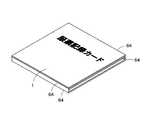
The present embodiment is an information recording device (also referred to as a circuit device) for recording the date and time when a patient takes a medicine and the condition after the medicine is taken, and FIG. 1 is an external view thereof. The information recording device shown in FIG. 1 is composed of a sheet-shaped medication recording card and is of a foldable type. When expanded, aninformation input surface 2 as shown in FIG. 2 appears. A medication recording card as theinformation recording device 1 includes apaper substrate 30 described later, aconductive circuit 18A provided on thepaper substrate 30, and a wireless transmission communication module connected to theconductive circuit 18A via acircuit connector 90. And 10 (see FIGS. 3 and 5).

このうち紙基板30と、この紙基板30上に設けられた導電回路18Aとにより、回路基板70が構成されている。なお、回路コネクタ90は必ずしも設ける必要はなく、また回路コネクタ90はフレキシブルなコネクタでも堅固なコネクタであってもよい。  Of these, thepaper board 30 and theconductive circuit 18A provided on thepaper board 30 constitute acircuit board 70. Thecircuit connector 90 does not always need to be provided, and thecircuit connector 90 may be a flexible connector or a rigid connector.

服薬記録カードからなる情報記録装置1について更に述べる。服薬記録カードは使用者、例えば患者が病院での診察を終えて、処方箋に基づいて薬の調合が終わった段階で患者に渡されるものである。この服薬記録カードでは、患者が薬を服用した後に、患者自ら選択ボタンを押圧して、体の具合を記録できるようにしている。  Theinformation recording device 1 including a medication recording card will be further described. The medication record card is given to the patient, for example, at the stage when the user, for example, the patient has completed the consultation at the hospital and has finished preparing the medicine based on the prescription. With this medication record card, after the patient has taken the medication, the patient himself / herself presses the selection button so that the physical condition of the patient can be recorded.

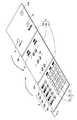
図2の服薬記録カードの情報入力面2は3面構成であり、第1面2aにはスタートボタン3と取り消しボタン4が設けられ、第2面2bには患者が服用すべき薬(錠剤)5が配置され、第3面2cには患者の症状の度合いを入力するための選択ボタンが配置されている。第1面2aの裏面側が図1の「服薬記録カード」と記載された面である。  Theinformation input surface 2 of the medication recording card of FIG. 2 has a three-sided configuration, a start button 3 and a cancel button 4 are provided on afirst surface 2a, and a medicine (tablet) to be taken by a patient is provided on a second surface 2b. 5, and a selection button for inputting the degree of the symptom of the patient is arranged on thethird surface 2c. The back side of thefirst surface 2a is the surface described as "medication recording card" in FIG.

第3面2cには、薬の効用に関連する複数の症状が記載されている。図2の例では、(1)症状1、(2)症状2、(3)症状3、(4)症状4および(5)症状5の計5種類の症状が記載され、各症状ごとに、3通りの度合い(重度、中度、軽度)から一つを選択可能になっている。患者は、まず、5種類の症状に対応する選択ボタン6a〜6eからなる第1ボタン列6のいずれかを押圧して、特定の症状を選択した後に、引き続いて、その症状の度合いに対応する選択ボタン7a〜7cからなる第2ボタン列7のいずれかを押圧する。これにより、患者は、薬を服用した後に特定の症状の度合いを入力できる。患者は、必ずしも5種類の症状のすべてに回答する必要はなく、一部の症状のみに回答してもよい。  Thethird surface 2c describes a plurality of symptoms related to the effect of the drug. In the example of FIG. 2, a total of five types of symptoms (1)symptom 1, (2)symptom 2, (3) symptom 3, (4) symptom 4 and (5) symptom 5 are described, and for each symptom, One of three levels (severe, medium, and mild) can be selected. The patient first presses any one of the first button rows 6 including theselection buttons 6a to 6e corresponding to the five types of symptoms to select a specific symptom, and subsequently, corresponds to the degree of the symptom. One of thesecond button rows 7 including theselection buttons 7a to 7c is pressed. This allows the patient to enter the degree of a particular symptom after taking the drug. The patient does not necessarily need to respond to all five symptoms, but may respond to only some of the symptoms.

第1ボタン列6を構成する各選択ボタン6a〜6eは図2のX方向に沿って配置され、第2ボタン列7を構成する各選択ボタンは、第1ボタン列6に略平行にY方向に沿って複数列にわたって配置されている。  Theselection buttons 6a to 6e forming the first button row 6 are arranged along the X direction in FIG. 2, and the selection buttons forming thesecond button row 7 are arranged substantially parallel to the first button row 6 in the Y direction. Are arranged over a plurality of rows.

なお、第3面2cに記載された症状とその度合いは、あくまで一例にすぎず、薬の種類によって任意に変更して構わない。  Note that the symptoms and their degrees described on thethird surface 2c are only examples, and may be arbitrarily changed depending on the type of the medicine.

患者は、服薬記録カードの使用を開始するときに、スタートボタン3を押圧する。その後、患者は、第2面2bに配置された錠剤5のケース5aを指で押し込んで、第2面2bの下面側から薬を取り出して、服用する。そして、服用後の症状の度合いに該当する選択ボタン6、7を押圧する。  The patient presses the start button 3 when starting to use the medication recording card. Thereafter, the patient pushes thecase 5a of the tablet 5 arranged on thesecond surface 2b with a finger, takes out the medicine from the lower surface side of thesecond surface 2b, and takes the medicine. Then, the user presses theselection buttons 6 and 7 corresponding to the degree of the symptom after taking the drug.

患者が押圧したスタートボタン3、取り消しボタン4、錠剤5の各ケースおよび各選択ボタン6、7の情報は、服薬記録カード内に内蔵された通信モジュール10に自動的に記憶される仕組みになっている。  The information of the start button 3, the cancel button 4, the case of the tablet 5, and theselection buttons 6, 7 pressed by the patient is automatically stored in thecommunication module 10 built in the medication recording card. I have.

図3は上述した無線通信可能な通信モジュール10の概略構成を示すブロック図である。図3の通信モジュール10は、樹脂基板11の上に実装されたICチップとしてのASIC(Application Specific Integrated Circuit)12と、水晶振動子13と、ボタン電池14と、スピーカ15と、樹脂基板11の長辺に沿って形成される複数のパッド16と、樹脂基板11の外縁部に沿って形成されるアンテナパターン17aと、樹脂基板11上に形成される導電パターン17bとを有する。  FIG. 3 is a block diagram showing a schematic configuration of thecommunication module 10 capable of wireless communication described above. Thecommunication module 10 shown in FIG. 3 includes an ASIC (Application Specific Integrated Circuit) 12 as an IC chip mounted on aresin substrate 11, acrystal unit 13, abutton battery 14, aspeaker 15, and aresin substrate 11. It has a plurality ofpads 16 formed along the long side, anantenna pattern 17a formed along the outer edge of theresin substrate 11, and aconductive pattern 17b formed on theresin substrate 11.

図3は通信モジュール10の内部構成を機能化したブロック図であり、実際の各回路部品やパターンの配置やサイズ、形状、個数は任意に変更可能である。  FIG. 3 is a block diagram in which the internal configuration of thecommunication module 10 is functionalized, and the arrangement, size, shape, and number of actual circuit components and patterns can be arbitrarily changed.

図4はASIC12の内部構成の一例を示すブロック図である。図4のASIC12は、患者が押圧したスタートボタン3、取り消しボタン4、錠剤5の各ケースおよび各選択ボタンの情報を時刻情報とともに時系列で記憶する記憶部21と、記憶部21に押圧情報を記憶する制御を行う制御部22と、不図示のホストコンピュータとの間で無線通信を行う無線通信部(出力インターフェース部)23とを有する。  FIG. 4 is a block diagram showing an example of the internal configuration of theASIC 12. TheASIC 12 of FIG. 4 stores a start button 3, a cancel button 4, a case of the tablet 5, and information of each of the selection buttons pressed by the patient in a time-series manner together with time information, and press information to thestorage unit 21. Thecontrol unit 22 includes acontrol unit 22 that performs control to store the information and a wireless communication unit (output interface unit) 23 that performs wireless communication with a host computer (not illustrated).

また制御部22は、患者がボタンを押圧した際、その押圧された情報を後述するフレキシブル確認回路100のLED発光部102を駆動させて発光させる。  Further, when the patient presses the button, thecontrol unit 22 drives the LEDlight emitting unit 102 of theflexible confirmation circuit 100, which will be described later, to emit the pressed information.

記憶部21は、患者が押圧したボタンを特定する情報と、そのボタンが押圧された時刻情報とを組にして記憶する。取り消しボタン4は、取り消しボタン4が押圧される直前に押圧されたボタンの情報を取り消すことを意図したものである。ホストコンピュータは、記憶部21に取り消しボタン4の押圧を特定する情報と、そのボタンが押圧された時刻情報とが記憶されている場合は、取り消しボタン4の直前に押圧されたボタンの情報を取り消す。  Thestorage unit 21 stores information specifying the button pressed by the patient and information on the time at which the button was pressed as a set. The cancel button 4 is intended to cancel the information of the button pressed immediately before the cancel button 4 is pressed. The host computer cancels the information of the button pressed immediately before the cancel button 4 when the information specifying the press of the cancel button 4 and the time information when the button was pressed are stored in thestorage unit 21. .

無線通信部23は、ホストコンピュータとの間で、いわゆるNFC(Near Field Communication、近接無線通信)やBluetooth(登録商標)等の非接触通信を行って、情報の送受を行う。無線通信部23が無線通信に用いる方式や周波数帯域は特に制限されるものではなく、例えば13.56MHzの帯域でISO14443に準拠した無線方式で無線通信を行い、Bluetoothの場合は規格で定めた周波数(例えば2.4GHz)で無線通信を行う。  Thewireless communication unit 23 transmits and receives information to and from a host computer by performing non-contact communication such as so-called Near Field Communication (NFC) or Bluetooth (registered trademark). The method and frequency band used by thewireless communication unit 23 for wireless communication are not particularly limited. For example, wireless communication is performed by a wireless method based on ISO14443 in a 13.56 MHz band, and in the case of Bluetooth, the frequency specified by the standard is used. (For example, 2.4 GHz).

NFCでは、規格上電力の送受もできるため、電池なしで通信モジュール10を駆動することも原理的には可能である。ただし、本実施形態の通信モジュール10は、スピーカ15も備えており、電力の消費量が比較的大きいため、ボタン電池14を搭載している。  In NFC, electric power can be transmitted and received according to the standard, so that it is possible in principle to drive thecommunication module 10 without a battery. However, thecommunication module 10 of the present embodiment is also provided with thespeaker 15 and consumes a relatively large amount of power.

次に、本実施形態に係る服薬記録カードの具体的構造について説明する。上述した服薬記録カード1は、1枚の紙基板を縦方向に三等分して折り畳んだ三層構造であり、その表面に図2に示す情報入力面2が現れるようにしている。これをさらに後述する折曲線64に沿って横方向に三等分して折り畳むと図1に示す構造になる。以下では、大元の1枚の紙基板に形成される導電パターンについて説明する。  Next, a specific structure of the medication recording card according to the present embodiment will be described. Themedication recording card 1 described above has a three-layer structure in which one paper substrate is vertically divided into three equal parts and folded, and theinformation input surface 2 shown in FIG. 2 appears on the surface thereof. When this is further folded into three equal parts in the lateral direction along afolding line 64, which will be described later, the structure shown in FIG. 1 is obtained. Hereinafter, the conductive pattern formed on one original paper substrate will be described.

図5は服薬記録カードの元となる紙基板30を展開した図である。図5の紙基板30を縦方向に延びる折り目61で三等分に分割した各分割基板30a、30b、30cには、それぞれ異なる導電パターン18や切り欠き等が設けられる。なお、これら3つの分割基板30a〜30cは、折り目61で折り曲げ可能とされており、物理的に切り離されるものではない。また、各分割基板30a、30b、30cは上述のように折曲線64を有し、各分割基板30a、30b、30cは横方向に延びる各々の折曲線64を介して三等分に折り畳まれる。図5において、便宜上、各分割基板30a、30b、30cには2本の単一の折曲線64が設けられているが単一の折曲線64の代わりに一対の平行する折曲線64、64を設けてもよい(図1参照)。  FIG. 5 is an expanded view of thepaper substrate 30 that is the basis of the medication record card. Differentconductive patterns 18 and cutouts are provided on each of the dividedsubstrates 30a, 30b, and 30c obtained by dividing thepaper substrate 30 of FIG. Note that these three dividedsubstrates 30a to 30c are bendable atfolds 61 and are not physically separated. Further, each of the dividedsubstrates 30a, 30b, 30c has thefolding line 64 as described above, and each of the dividedsubstrates 30a, 30b, 30c is folded into three equal parts via each of the laterally extending folding lines 64. In FIG. 5, for convenience, each of the dividedsubstrates 30a, 30b, 30c is provided with two single folding curves 64, but instead of thesingle folding curve 64, a pair of parallel folding curves 64, 64 are provided. It may be provided (see FIG. 1).

図5の中央の分割基板30bは、最下層に配置されて導電パターン18が形成される最下層基板30bである。その右側の分割基板30cは、主に切り欠き62とミシン目63を有し、最下層基板30bの上に配置される中間層基板30cである。最下層基板30bの左側の分割基板30aは、スイッチ接点の導通/遮断を行う導電パターン38を有し、中間層基板30cの上に配置される最上層基板30aである。  The dividedsubstrate 30b in the center of FIG. 5 is thelowermost layer substrate 30b arranged on the lowermost layer and having theconductive pattern 18 formed thereon. The dividedsubstrate 30c on the right side is anintermediate layer substrate 30c mainly having anotch 62 and aperforation 63 and arranged on thelowermost substrate 30b. The dividedsubstrate 30a on the left side of thelowermost layer substrate 30b is theuppermost layer substrate 30a, which has theconductive pattern 38 for connecting / disconnecting the switch contacts and is arranged on theintermediate layer substrate 30c.

後述するように、三等分された最下層基板30bに中間層基板30cを折り畳んで熱圧着した後に、その上に錠剤5を収納するケース5a含む成形シートを載せ、その上に最上層基板30aを折り畳んで熱圧着することにより、図2の構造が得られる。したがって、図5に示す最上層基板30aの裏面側が、図2に示す情報入力面2になる。  As will be described later, after folding theintermediate layer substrate 30c on thelowermost layer substrate 30b divided into three parts and thermocompression bonding, a molding sheet containing acase 5a for storing the tablets 5 is placed thereon, and theuppermost layer substrate 30a is placed thereon. The structure of FIG. 2 is obtained by folding and thermocompression bonding. Therefore, the back side of theuppermost substrate 30a shown in FIG. 5 becomes theinformation input surface 2 shown in FIG.

最下層基板30bの上に中間層基板30cを折り畳んで熱圧着する前に、最下層基板30bに通信モジュール10が接合され、その上に最上層基板30aが熱圧着される。このように、通信モジュール10は、最下層基板30bと最上層基板30aの間に挟み込まれる。これにより、最下層基板30bの表面に形成された導電パターン18と通信モジュール10は、服薬記録カードの完成状態では、外見に現れない。同様に、最上層基板30a上の導電パターンも、中間層基板30cの上に折り畳まれて熱圧着されるため、外見に現れない。  Before folding and thermocompression bonding theintermediate layer substrate 30c on thelowermost substrate 30b, thecommunication module 10 is joined to thelowermost substrate 30b, and theuppermost substrate 30a is thermocompressed thereon. In this way, thecommunication module 10 is sandwiched between thelowermost layer substrate 30b and theuppermost layer substrate 30a. As a result, theconductive pattern 18 and thecommunication module 10 formed on the surface of thelowermost substrate 30b do not appear in the finished state of the medication recording card. Similarly, the conductive pattern on theuppermost layer substrate 30a does not appear on the outside because it is folded and thermocompression-bonded on theintermediate layer substrate 30c.

次に、最下層基板30bの表面に形成された導電パターン18について図5を用いて説明する。図5の導電パターン18は、三等分された第1〜第3面2a〜2cからなる情報入力面2に対応した第1〜第3パターン面30b1〜30b3を有する。  Next, theconductive pattern 18 formed on the surface of thelowermost substrate 30b will be described with reference to FIG. Theconductive pattern 18 of FIG. 5 has first to third pattern surfaces 30b1 to 30b3 corresponding to theinformation input surface 2 composed of the first tothird surfaces 2a to 2c divided into three equal parts.

第1パターン面30b1は、スタートボタン3に対応したスイッチ接点31と、取り消しボタン4に対応したスイッチ接点32とを有する。第2パターン面30b2は、錠剤5の各ケースに対応した計6つのスイッチ接点33を有する。第3パターン面30b3は、患者の症状および症状の程度を選択する各選択ボタンに対応した計15個のスイッチ接点34〜37を有する。  The first pattern surface 30b1 has aswitch contact 31 corresponding to the start button 3 and aswitch contact 32 corresponding to the cancel button 4. The second pattern surface 30b2 has a total of sixswitch contacts 33 corresponding to each case of the tablet 5. The third pattern surface 30b3 has a total of 15switch contacts 34 to 37 corresponding to each selection button for selecting the symptom and the degree of the symptom of the patient.

これらスイッチ接点31〜37のうち、錠剤5の各ケースに5a対応した計6つのスイッチ接点33は初期状態で導通しており、それ以外の全てのスイッチ接点31、32、34〜37は初期状態で遮断されている。  Of theseswitch contacts 31 to 37, a total of sixswitch contacts 33 corresponding to eachcase 5a of the tablet 5 are conductive in the initial state, and allother switch contacts 31, 32, 34 to 37 are in the initial state. Is shut off by

錠剤5の各ケース5aに対応したスイッチ接点33は、ケース5aを押圧して錠剤5を取り出す際に物理的に破断されて、電気的導通が遮断される。それ以外のスイッチ接点31、32、34〜37は、対応するボタンを押圧したときに、情報入力面2の裏面側に設けられた円形の導電パターン38が対応するスイッチ接点に接触して、押圧している間だけ一時的に導通する。  Theswitch contacts 33 corresponding to eachcase 5a of the tablet 5 are physically broken when thecase 5a is pressed and the tablet 5 is taken out, and the electrical conduction is cut off. Theother switch contacts 31, 32, 34 to 37 are pressed when the corresponding button is pressed, and the circularconductive pattern 38 provided on the back side of theinformation input surface 2 comes into contact with the corresponding switch contact. Conduction only temporarily during the operation.

このように、スイッチ接点31〜37の中には、初期状態で電気的に導通しているものと、電気的に遮断されているものとがある。各スイッチ接点を物理的に破断するか、各スイッチ接点に別の導電パターンを接触させることにより、スイッチ接点の状態を切り替えることができる。  As described above, some of theswitch contacts 31 to 37 are electrically conductive in an initial state and some are electrically disconnected. The state of the switch contacts can be switched by physically breaking each switch contact or bringing another conductive pattern into contact with each switch contact.

図5に示す各スイッチ接点31〜37の一端は、導電パターン18を介して第1パターン面30b1上の端子部39の対応する端子に接続され、他端はいずれも導電パターン18を介して接地端子に接続されている。端子部39には、スイッチ接点の総数分の端子が設けられ、これに加えて、端子部39の両端側には接地端子が設けられている。接地端子から延びる導電パターン(以下、接地パターン18a)は、第1〜第3パターン面30b3の外縁に沿って、他の導電パターンとスイッチ接点を取り囲むように形成されている。  One end of each of theswitch contacts 31 to 37 shown in FIG. 5 is connected to the corresponding terminal of theterminal portion 39 on the first pattern surface 30b1 via theconductive pattern 18, and the other ends are all grounded via theconductive pattern 18. It is connected to the terminal.Terminals 39 are provided with terminals for the total number of switch contacts, and in addition, ground terminals are provided on both ends of the terminal 39. A conductive pattern (hereinafter,ground pattern 18a) extending from the ground terminal is formed along the outer edges of the first to third pattern surfaces 30b3 so as to surround other conductive patterns and switch contacts.

この接地パターン18aは、ノイズの低減を図るために、他の導電パターンよりも太く形成されている。  Theground pattern 18a is formed thicker than the other conductive patterns in order to reduce noise.

ここで上述した導電パターン18と接地パターン18aとにより、導電回路18Aが構成される。また導電回路18Aに端子部39が接続される。また紙基板30と、紙基板30上に形成された導電回路18Aとにより通信モジュール10が接合される前の回路基板70が構成される。  Here, theconductive pattern 18 and theground pattern 18a form aconductive circuit 18A. Further, theterminal portion 39 is connected to theconductive circuit 18A. Further, thecircuit board 70 before thecommunication module 10 is joined is constituted by thepaper board 30 and theconductive circuit 18A formed on thepaper board 30.

このように、すべてのスイッチ接点が、対応する端子と接地パターン18aとの間に接続されている。したがって、いずれかのスイッチ接点の状態が変化すると、その変化した情報が、専用の端子を介して通信モジュール10に伝達されることになる。通信モジュール10内の記憶部21は、接点の状態が変化したスイッチ接点を特定する情報と、すなわち押圧された選択ボタンまたは破断位置を特定する情報と、接点の状態が変化した時刻情報とを記憶する。  Thus, all the switch contacts are connected between the corresponding terminals and theground pattern 18a. Therefore, when the state of any of the switch contacts changes, the changed information is transmitted to thecommunication module 10 via the dedicated terminal. Thestorage unit 21 in thecommunication module 10 stores information for specifying a switch contact whose contact state has changed, that is, information for specifying a pressed selection button or a break position, and time information for a change in the contact state. I do.

第3パターン面30b3上の各スイッチ接点は、X方向に沿って配置される第1ボタン列に対応する第1スイッチ接点列34と、第1ボタン列に略平行にY方向に沿って配置される複数の第2ボタン列に対応する複数の第2スイッチ接点列35〜37とにグループ分けされている。  Each switch contact on the third pattern surface 30b3 is arranged along the Y direction substantially parallel to the firstswitch contact row 34 corresponding to the first button row arranged along the X direction. Are grouped into a plurality of secondswitch contact rows 35 to 37 corresponding to the plurality of second button rows.

第2スイッチ接点列35〜37のそれぞれにおける計5個のスイッチ接点の一端側はいずれも共通の端子に接続され、他端側はいずれも接地端子に接続されており、これら5個のスイッチ接点は並列接続されている。図5の例では、計5個のスイッチ接点が並列接続された第2スイッチ接点列35〜37が計3個設けられている。  One end of each of the five switch contacts in each of the secondswitch contact rows 35 to 37 is connected to a common terminal, and the other end is connected to a ground terminal. Are connected in parallel. In the example of FIG. 5, a total of three secondswitch contact rows 35 to 37 in which a total of five switch contacts are connected in parallel are provided.

並列接続された各スイッチ接点列35〜37内のどのスイッチ接点の状態が変化しても、その状態変化情報は同じ端子を介して通信モジュール10に伝達されるため、通信モジュール10では、どのスイッチ接点が変化したのかをその情報だけでは特定できない。そこで、本実施形態では、第2スイッチ接点列35〜37内のスイッチ接点の状態を変化させる前に、第1スイッチ接点列34内のスイッチ接点の状態を変化させるようにルール化することで、第2スイッチ接点列35〜37内のどのスイッチ接点の状態が変化したかを特定している。  Even if the state of any switch contact in each of theswitch contact rows 35 to 37 connected in parallel changes, the state change information is transmitted to thecommunication module 10 through the same terminal. Whether or not the contact has changed cannot be specified by the information alone. Therefore, in the present embodiment, before changing the state of the switch contacts in the secondswitch contact row 35 to 37, a rule is formed so that the state of the switch contacts in the firstswitch contact row 34 is changed. Which of the switch contacts in the secondswitch contact rows 35 to 37 has changed has been specified.

より具体的には、まず第1スイッチ接点列34内のいずれかのスイッチ接点の状態を変化させて、このスイッチ接点のX方向位置を検出する。そして、同じX方向位置にある第2スイッチ接点列35〜37内の計3個のスイッチ接点を選択候補として決定する。次に、これら3個のスイッチ接点の中で、状態が変化したものがあれば、そのスイッチ接点の情報を通信モジュール10に伝達する。  More specifically, first, the state of any of the switch contacts in the firstswitch contact row 34 is changed to detect the position of the switch contact in the X direction. Then, a total of three switch contacts in the secondswitch contact rows 35 to 37 located at the same X direction position are determined as selection candidates. Next, if any of these three switch contacts has changed state, the information of the switch contact is transmitted to thecommunication module 10.

このように、第1スイッチ接点列34内のスイッチ接点の状態変化情報と、第2スイッチ接点列35〜37内のスイッチ接点の状態変化情報とを組み合わせることで、第2スイッチ接点列35〜37内の特定のスイッチ接点の状態を正しく通信モジュール10に伝達することができる。  As described above, by combining the state change information of the switch contacts in the firstswitch contact row 34 with the state change information of the switch contacts in the secondswitch contact rows 35 to 37, the secondswitch contact rows 35 to 37 are combined. The state of the specific switch contact in thecommunication module 10 can be transmitted to thecommunication module 10 correctly.

複数のスイッチ接点を並列接続して、一端側を共通の端子に接続することは、端子部39内の端子の総数と導電パターン18の数を削減できることから、特にパターン面積が限られている場合に有効である。第2スイッチ接点列35〜37内の複数のスイッチ接点を並列接続しても、第2スイッチ接点列35〜37と平行に配置された第1スイッチ接点列34内のスイッチ接点の状態と組み合わせることで、第2スイッチ接点列35〜37内の特定のスイッチ接点の状態を正確に特定できるため、実用上の問題は起きない。
このように、本実施形態に係る服薬記録カード1は、スタートボタン3や各種の選択ボタンの他に、直前のボタン操作を取り消すための取り消しボタン4を具備するため、ボタンの誤操作による誤った情報が取消情報なく通信モジュール10に伝達されるおそれがなくなり、通信モジュール10およびホストコンピュータに伝達される情報の信頼性が向上する。
When a plurality of switch contacts are connected in parallel and one end side is connected to a common terminal, the total number of terminals in theterminal portion 39 and the number ofconductive patterns 18 can be reduced. Therefore, especially when the pattern area is limited. Is effective for. Even if a plurality of switch contacts in the secondswitch contact rows 35 to 37 are connected in parallel, the plurality of switch contacts are combined with the state of the switch contacts in the firstswitch contact row 34 arranged in parallel with the secondswitch contact rows 35 to 37. Thus, since the state of the specific switch contact in the secondswitch contact row 35 to 37 can be accurately specified, no practical problem occurs.
As described above, themedication recording card 1 according to the present embodiment includes the cancel button 4 for canceling the immediately preceding button operation in addition to the start button 3 and various selection buttons, so that erroneous information due to erroneous operation of the button is provided. Is not transmitted to thecommunication module 10 without cancellation information, and the reliability of the information transmitted to thecommunication module 10 and the host computer is improved.

ところで、上述のように各分割基板30a、30b、30cは、横方向に延びる各々の折曲線64を介して三等分に折り畳まれる。  By the way, as described above, the dividedsubstrates 30a, 30b, 30c are folded into three equal parts via therespective folding lines 64 extending in the lateral direction.

このうち最下層基板30bには、導電パターン18と接地パターン18aとからなる導電回路18Aが設けられている。また最下層基板30bの折曲線64近傍には、折曲線64を介して最下層基板30bを繰り返し折り曲げた場合でも、導電回路18Aが破断したり破損することを防止するため、フレキシブル回路コネクタ80A、80Bが設けられている。  Aconductive circuit 18A including aconductive pattern 18 and aground pattern 18a is provided on thelowermost layer substrate 30b. Further, in the vicinity of thefolding line 64 of thelowermost layer substrate 30b, even when thelowermost layer substrate 30b is repeatedly folded through thefolding line 64, in order to prevent theconductive circuit 18A from being broken or damaged, theflexible circuit connector 80A, 80B is provided.

具体的には最下層基板30bは、横方向に延びる2本の折曲線64を介して三等分に折り畳まれるが、この場合、最下層基板30bは2本の折曲線64により、第1基板91と第2基板92と第3基板95とに区画され、第1基板91と第2基板92との間に折曲線64を跨いでフレキシブル回路コネクタ80Aが設けられ、第2基板92と第3基板95との間に折曲線64を跨いでフレキシブル回路コネクタ80Bが設けられている。  Specifically, thelowermost layer substrate 30b is folded into three equal parts through twofolding lines 64 extending in the lateral direction. In this case, thelowermost layer substrate 30b is bent by the twofolding lines 64 to form the first substrate. 91, thesecond substrate 92, and thethird substrate 95, and theflexible circuit connector 80A is provided between thefirst substrate 91 and thesecond substrate 92 across thefolding curve 64, and thesecond substrate 92 and thethird substrate 95 are provided. Aflexible circuit connector 80B is provided across thefold line 64 between itself and thesubstrate 95.

フレキシブル回路コネクタ80A、80Bは、略同様の構造をもつため、ここではフレキシブル回路コネクタ80Aについて図6Aおよび図6Bにより説明する。  Since theflexible circuit connectors 80A and 80B have substantially the same structure, theflexible circuit connector 80A will be described here with reference to FIGS. 6A and 6B.

図6Aおよび図6Bに示すように、導電回路18Aのうち第1基板91上の導電回路は、第1導電回路93となっており、第2基板92上の第2導電回路94となっている。  As shown in FIGS. 6A and 6B, the conductive circuit on thefirst substrate 91 of theconductive circuit 18A is the firstconductive circuit 93 and the secondconductive circuit 94 on thesecond substrate 92. .

フレキシブル回路コネクタ80Aは最下層基板30bのうち、折曲線64を介して連結された第1基板91と第2基板92との間に折曲線64を跨いで設けられ、第1基板91側の第1導電回路93と第2基板92側の第2導電回路94とを接続するものである。この場合、第1基板91上の第1導電回路93と第2基板92上の第2導電回路94は互いに離間し、フレキシブル回路コネクタ80Aを設けることにより、初めて導通するようになっている。しかしながら、フレキシブル回路コネクタ80Aがない場合でも、第1基板91上の第1導電回路93と第2基板92上の第2導電回路94を接続しておいてもよい。この場合、フレキシブル回路コネクタ80Aは、第1導電回路93と第2導電回路94が切断した際のバックアップ回路として機能する。  Theflexible circuit connector 80A is provided on thelowermost layer substrate 30b between thefirst substrate 91 and thesecond substrate 92, which are connected to each other via thefolding line 64, across thefolding line 64, and is located on thefirst substrate 91 side. The oneconductive circuit 93 is connected to the secondconductive circuit 94 on thesecond substrate 92 side. In this case, the firstconductive circuit 93 on thefirst substrate 91 and the secondconductive circuit 94 on thesecond substrate 92 are separated from each other and theflexible circuit connector 80A is provided so that the firstconductive circuit 93 and the secondconductive circuit 94 are electrically connected. However, even if theflexible circuit connector 80A is not provided, the firstconductive circuit 93 on thefirst substrate 91 and the secondconductive circuit 94 on thesecond substrate 92 may be connected. In this case, theflexible circuit connector 80A functions as a backup circuit when the firstconductive circuit 93 and the secondconductive circuit 94 are disconnected.

次にフレキシブル回路コネクタ80Aについて更に述べる。  Next, theflexible circuit connector 80A will be further described.

図5、図6Aおよび図6Bに示すように、フレキシブル回路コネクタ80Aは、絶縁性基材81と、絶縁性基材81の一側に設けられた一側端子部83と、絶縁性基材81の他側に設けられた他側端子部84と、これら一側端子部83と他側端子部84とを接続する複数の導電部(導電インキ)82とを有する。  As shown in FIGS. 5, 6A, and 6B, theflexible circuit connector 80A includes an insulatingbase material 81, a one-side terminal portion 83 provided on one side of the insulatingbase material 81, and an insulatingbase material 81. The otherside terminal portion 84 provided on the other side, and a plurality of conductive portions (conductive ink) 82 connecting the oneside terminal portion 83 and the otherside terminal portion 84.

この場合、導電部82は一側端子部83から他側端子部84まで直線状に延びている。  In this case, theconductive portion 82 extends linearly from the oneside terminal portion 83 to the otherside terminal portion 84.

また一側端子部83および他側端子部84上には、ヒートシール時に異方導電性能を発現する異方導電性接着剤87が設けられている。  An anisotropic conductive adhesive 87 that exhibits anisotropic conductive performance during heat sealing is provided on the oneterminal 83 and theother terminal 84.

ところで、一側端子部83は第1基板91上の第1導電回路93に接続される端子部であり、他側端子部84は第2基板92上の第2導電回路94に接続される端子部である。  By the way, the one-side terminal portion 83 is a terminal portion connected to the firstconductive circuit 93 on thefirst substrate 91, and the other-side terminal portion 84 is a terminal connected to the secondconductive circuit 94 on thesecond substrate 92. It is a department.

また絶縁性基材81上には、一側端子部83と一側端子部83上の異方導電性接着剤87、他側端子部84と他側端子部84上の異方導電性接着剤87を露出させ、導電部82上を覆ってアクリルからなる絶縁層88が設けられている。  Further, on the insulatingbase material 81, the one-side terminal portion 83 and the anisotropic conductive adhesive 87 on the one-side terminal portion 83, and the other-side terminal portion 84 and the anisotropic conductive adhesive on the other-side terminal portion 84. An insulatinglayer 88 made of acrylic is provided to expose 87 and cover theconductive portion 82.

絶縁層88の材質としては、特に限定はなく、ビニル系、ゴム系などの材料を使用できる。また、図7Aに示すように、フレキシブル回路コネクタ80の絶縁層88として、異方導電性接着剤製のものを使用することもできる。  The material of the insulatinglayer 88 is not particularly limited, and a vinyl-based or rubber-based material can be used. As shown in FIG. 7A, the insulatinglayer 88 of the flexible circuit connector 80 may be made of an anisotropic conductive adhesive.

図7Aにおいて、導電部82上に同一の異方導電性接着剤を印刷することにより、異方導電性接着剤からなり異方導電性能を発現する予定となる異方導電性能発現予定部87aと、異方導電性能を発現しない異方導電性接着剤製の絶縁層88とを同時に形成することができ、製造効率の向上を図ることができる。  In FIG. 7A, by printing the same anisotropic conductive adhesive on theconductive portion 82, an anisotropic conductiveperformance developing portion 87a made of an anisotropic conductive adhesive and exhibiting anisotropic conductive performance is provided. In addition, the insulatinglayer 88 made of an anisotropic conductive adhesive which does not exhibit anisotropic conductive performance can be formed at the same time, and the production efficiency can be improved.

図7Bに示すように、フレキシブル回路コネクタ80Aを第1導電回路93または第2導電回路94にヒートシールする際、異方導電性接着剤からなる異方導電性能発現予定部87aがヒートシールされて、異方導電性能を発現する異方導電性能発現部87bに変わる。図7Bにおいて、絶縁層88は、異方導電性接着剤からなるが、異方導電性能は発現していない。  As shown in FIG. 7B, when theflexible circuit connector 80A is heat-sealed to the firstconductive circuit 93 or the secondconductive circuit 94, the anisotropic conductiveperformance exhibiting portion 87a made of an anisotropic conductive adhesive is heat-sealed. , The anisotropic conductiveperformance developing portion 87b that develops the anisotropic conductive performance. In FIG. 7B, the insulatinglayer 88 is made of an anisotropic conductive adhesive, but does not exhibit anisotropic conductive performance.

なお、フレキシブル回路コネクタ80の絶縁性基材81は、柔軟性基材、例えばポリエチレンテレフタレートまたはポリブチレンテレフタレート製の基材からなる。そしてフレキシブル回路コネクタ80は一側端子部83および他側端子部84を下方に向けて、一側端子部83と第1基板91の第1導電回路93を接続させ、他側端子部84と第2基板92の第2導電回路94とを接続させて、第1導電回路93と第2導電回路94とを接続する(図6Aおよび図6B参照)。  The insulatingbase material 81 of the flexible circuit connector 80 is made of a flexible base material such as polyethylene terephthalate or polybutylene terephthalate. The flexible circuit connector 80 directs the one-side terminal portion 83 and the other-side terminal portion 84 downward to connect the one-side terminal portion 83 and the firstconductive circuit 93 of thefirst substrate 91, and the other-side terminal portion 84 and the firstconductive circuit 93. The secondconductive circuit 94 of thesecond substrate 92 is connected to connect the firstconductive circuit 93 and the second conductive circuit 94 (see FIGS. 6A and 6B).

このように最下層基板30bの第1基板91と第2基板92との間に折曲線64を跨いで、第1導電回路93と第2導電回路94を接続してフレキシブル回路コネクタ80Aを設けることにより、最下層基板30bを折曲線64を介して繰り返し折り曲げたり拡げたりした場合であっても、フレキシブル回路コネクタ80Aが破断することはない。このことにより、第1基板91の第1導電回路93と第2基板92の第2導電回路94との間で、破断したり破損することなく、常に安定的に第1導電回路93と第2導電回路94との間の導通を得ることができる。  In this way, theflexible circuit connector 80A is provided by connecting the firstconductive circuit 93 and the secondconductive circuit 94 across thefolding curve 64 between thefirst substrate 91 and thesecond substrate 92 of thelowermost layer substrate 30b. Therefore, even when thelowermost layer substrate 30b is repeatedly bent or expanded through thefolding curve 64, theflexible circuit connector 80A does not break. As a result, the firstconductive circuit 93 of thefirst substrate 91 and the secondconductive circuit 94 of thesecond substrate 92 are not stably broken or damaged, and the firstconductive circuit 93 and the secondconductive circuit 93 are always stable. Conduction with theconductive circuit 94 can be obtained.

また上述のように、紙基板30のうち分割基板30bに、通信モジュール10が配置されるが、この分割基板30bと通信モジュール10との間にフレキシブル確認回路100が介在される(図5参照)。このフレキシブル確認回路100はいずれかのボタン、例えばスタートボタン3、取り消しボタン4、錠剤5のケース5a、選択ボタン6および選択ボタン7のいずれかのボタンが押圧された際に、この押圧確認を行うLED発光部102等の押圧確認手段を含む。図5において、このLED発光部102は通信モジュール10の右端から手前側へ露出している。  As described above, thecommunication module 10 is arranged on the dividedboard 30b of thepaper board 30, and theflexible confirmation circuit 100 is interposed between the dividedboard 30b and the communication module 10 (see FIG. 5). . Theflexible confirmation circuit 100 confirms the press when any one of the buttons, for example, the start button 3, the cancel button 4, thecase 5a of the tablet 5, the select button 6 and theselect button 7 is pressed. A pressing confirmation means such as the LEDlight emitting unit 102 is included. In FIG. 5, the LEDlight emitting unit 102 is exposed from the right end of thecommunication module 10 to the front side.

具体的には、図5および図8に示すように、フレキシブル確認回路100はビニル系、ゴム系の材料からなる絶縁性のフレキシブル基材101と、このフレキシブル基材101上に実装されたLED発光部102と、フレキシブル基材101上に設けられ、LED発光部102と通信モジュール10とを接続するとともに、線状に形成された導電部103とを有する。  Specifically, as shown in FIGS. 5 and 8, theflexible confirmation circuit 100 includes an insulatingflexible base material 101 made of a vinyl-based or rubber-based material, and an LED light emitting device mounted on theflexible base material 101. It has aportion 102 and aconductive portion 103 which is provided on theflexible base material 101, connects the LEDlight emitting portion 102 and thecommunication module 10, and is formed in a linear shape.

ここで、図8は分割基板30bに配置される通信モジュールの裏面と、この通信モジュール10の裏面上に取付けられたフレキシブル確認回路100とを示す。  Here, FIG. 8 shows the back surface of the communication module arranged on the dividedsubstrate 30b, and theflexible confirmation circuit 100 mounted on the back surface of thecommunication module 10.

そしてフレキシブル確認回路100のLED発光部102は、紙基板30のうち分割基板30aに形成された発光部用窓105を介して外方へ露出する。そしてLED発光部102は、ボタン3、4、5a、6および7のうちいずれかのボタンが患者により押圧された際、通信モジュール10の制御部22により発光して発光部用窓105から発光状態を外方へ現わすようになっている。  The LEDlight emitting portion 102 of theflexible confirmation circuit 100 is exposed to the outside through the light emittingportion window 105 formed on the dividedsubstrate 30a of thepaper substrate 30. When one of thebuttons 3, 4, 5a, 6 and 7 is pressed by the patient, the LEDlight emitting unit 102 emits light by thecontrol unit 22 of thecommunication module 10 and emits light from the light emittingunit window 105. To the outside.

このようにLED発光部102は、ボタンが押圧された際に押圧確認を行う押圧確認手段として機能するが、このような押圧確認手段として他の押圧確認手段、例えば他の発光部を用いてもよく、発光部以外に押圧確認手段としては振動を発生させる振動子を用いてもよい。さらに、押圧確認手段として、発光部と振動子を組み合わせてもよい。  As described above, the LEDlight emitting unit 102 functions as a pressing confirmation unit that confirms pressing when a button is pressed, but other pressing confirming units, such as another light emitting unit, may be used as such a pressing confirming unit. Alternatively, a vibrator that generates vibration may be used as the pressing confirmation means other than the light emitting unit. Further, a light emitting unit and a vibrator may be combined as the pressing confirmation means.

ところでLED発光部102としては、例えばチップ状のLED素子を用いることができ、LED発光部102の電源は通信モジュール10内のボタン電池から供給される。  Incidentally, for example, a chip-shaped LED element can be used as the LEDlight emitting unit 102, and power of the LEDlight emitting unit 102 is supplied from a button battery in thecommunication module 10.

次に、紙基板30に対してフレキシブル確認回路100を設置する方法について図5および図8により説明する。  Next, a method of installing theflexible confirmation circuit 100 on thepaper substrate 30 will be described with reference to FIGS.

まずフレキシブル基材101上に印刷等により線状の導電部103が形成され、この導電部103の一側端部(図8の左側端部)に、チップ状のLED素子からなるLED発光部102が導電性接着剤等により実装される。このようにしてフレキシブル基材101と、導電部103と、LED発光部102とを有するフレキシブル確認回路100が構成される。  First, a linearconductive portion 103 is formed on aflexible base material 101 by printing or the like, and one end (the left end in FIG. 8) of theconductive portion 103 is provided with an LEDlight emitting portion 102 including a chip-shaped LED element. Is mounted with a conductive adhesive or the like. In this way, theflexible confirmation circuit 100 including theflexible base material 101, theconductive portion 103, and the LEDlight emitting portion 102 is configured.

次に、このようにして構成されたフレキシブル確認回路100は、導電部103およびLED発光部102を通信モジュール10側へ向けて、通信モジュール10の裏面に取付けられる。本実施形態においては、フレキシブル確認回路100は、通信モジュール10のスピーカ端子部に接続されている。この場合、スタートボタン3、取り消しボタン4、錠剤5のケース5a、選択ボタン6および選択ボタン7のいずれかのボタンが押圧された際にスピーカからブザー音が鳴るように設定しておくことで、ブザー音に連動してLED発光部102が発光する。また、ボタン毎にブザー音を変えておくとLEDの発光も変化する為、発光状態でどのボタンが押されたか視覚的に確認することが可能になる。  Next, theflexible confirmation circuit 100 thus configured is mounted on the back surface of thecommunication module 10 with theconductive part 103 and the LEDlight emitting part 102 facing thecommunication module 10 side. In the present embodiment, theflexible confirmation circuit 100 is connected to the speaker terminal of thecommunication module 10. In this case, when any one of the start button 3, the cancel button 4, thecase 5a of the tablet 5, the select button 6, and theselect button 7 is pressed, the buzzer sounds from the speaker so that the buzzer sounds. The LEDlight emitting unit 102 emits light in conjunction with the buzzer sound. Further, if the buzzer sound is changed for each button, the light emission of the LED also changes, so that it is possible to visually confirm which button has been pressed in the light emitting state.

このとき、通信モジュール10は、フレキシブル確認回路100の導電部103の他側端部(図8の右側端部)に導電性接着剤を用いて接続される。  At this time, thecommunication module 10 is connected to the other end (the right end in FIG. 8) of theconductive portion 103 of theflexible confirmation circuit 100 using a conductive adhesive.

このように予めフレキシブル確認回路100と通信モジュール10とを接続しておき、互いに接続された通信モジュール10とフレキシブル確認回路は、その後、紙基板30の分割基板30b上に載置される。  As described above, theflexible confirmation circuit 100 and thecommunication module 10 are connected in advance, and thecommunication module 10 and the flexible confirmation circuit connected to each other are then mounted on the dividedsubstrate 30b of thepaper substrate 30.

この際、通信モジュール10は分割基板30b上に設けられた導電回路18Aに、回路コネクタ90を介して接続される。  At this time, thecommunication module 10 is connected to theconductive circuit 18A provided on the dividedsubstrate 30b via thecircuit connector 90.

使用に際して、患者(使用者)がいずれかのボタン、例えばスタートボタン3、取り消しボタン4、錠剤5のケース5a、選択ボタン6および選択ボタン7のうちいずれかのボタンを押圧した際、通信モジュール10の制御部22により、フレキシブル確認回路100のLED発光部102を発光させる。このときLED発光部102の発光状態は、発光部用窓105から外方へ現れる。このことにより、患者は、自らがいずれかのボタンを押圧したことを直ちに確認することができる。  In use, when the patient (user) presses any one of the buttons, for example, the start button 3, the cancel button 4, thecase 5 a of the tablet 5, the select button 6 and theselect button 7, thecommunication module 10 Thecontrol unit 22 causes the LEDlight emitting unit 102 of theflexible confirmation circuit 100 to emit light. At this time, the light emitting state of the LEDlight emitting unit 102 appears outward from the light emittingunit window 105. This allows the patient to immediately confirm that he or she has pressed any of the buttons.

一般に紙基板30に設けられたボタン3、4、5a、6、7を押圧した場合、この押圧したという感覚はボタンから得ることはできない。このためボタン3、4、5a、6、7を押圧しても押圧したか否か不安になることも考えられるが、本実施の形態によれば、ボタン3、4、5a、6、7を押圧した場合、患者は直ちに発光部用窓105を介してLED発光部102の発光状態を確認することができるため、ボタンを押圧したことを直ちに確認することができる。  Generally, when thebuttons 3, 4, 5a, 6, and 7 provided on thepaper substrate 30 are pressed, the feeling of the pressing cannot be obtained from the buttons. For this reason, even if thebuttons 3, 4, 5 a, 6, and 7 are pressed, it may be unclear whether or not thebuttons 3, 4, 5 a, 6, and 7 are pressed. When the button is pressed, the patient can immediately confirm the light emitting state of the LEDlight emitting unit 102 through the light emittingunit window 105, and thus can immediately confirm that the button is pressed.

また、フレキシブル確認回路100は、予めフレキシブル基材101上にLED発光部102を実装することにより得られ、このようにして得られたフレキシブル確認回路100を通信モジュール10に簡単に接続することができる。またフレキシブル確認回路100が接続された通信モジュール10は、紙基板30の分割基板30b上に設けられた導電回路18Aに回路コネクタ90を介して接続されるため、紙基板30にて対して通信モジュール10およびフレキシブル確認回路100を容易かつ簡単に取り付けることができる。  Also, theflexible confirmation circuit 100 is obtained by mounting the LEDlight emitting unit 102 on theflexible base material 101 in advance, and theflexible confirmation circuit 100 thus obtained can be easily connected to thecommunication module 10. . Further, since thecommunication module 10 to which theflexible confirmation circuit 100 is connected is connected to theconductive circuit 18A provided on the dividedsubstrate 30b of thepaper substrate 30 via thecircuit connector 90, the communication module is connected to thepaper substrate 30. 10 and theflexible confirmation circuit 100 can be attached easily and easily.

すなわち、フレキシブル確認回路100を用いることなく、紙基板30の分割基板30b上にLED発光部を設け、このLED発光部と通信モジュールを別個の導電線に接続することも考えられるが、導電線の引き回し作業、あるいは導電部と通信モジュールおよびLED発光部との接続作業を紙基板30上で実行する必要があり、接続作業は煩雑である。  That is, it is conceivable that an LED light emitting unit is provided on the dividedsubstrate 30b of thepaper substrate 30 without using theflexible confirmation circuit 100, and the LED light emitting unit and the communication module are connected to separate conductive lines. It is necessary to carry out the wiring work or the connection work of the conductive part and the communication module and the LED light emitting part on thepaper substrate 30, and the connection work is complicated.

これに対して本実施の形態によれば、予めフレキシブル確認回路100と通信モジュール10とを接続しておき、紙基板30に対して互いに接続された通信モジュール10およびフレキシブル確認回路100を取り付けるため、通信モジュール10およびフレキシブル確認回路100を容易かつ簡単に紙基板30に対して取付けることができる。  On the other hand, according to the present embodiment, since theflexible confirmation circuit 100 and thecommunication module 10 are connected in advance and thecommunication module 10 and theflexible confirmation circuit 100 connected to each other are attached to thepaper substrate 30, Thecommunication module 10 and theflexible confirmation circuit 100 can be easily and easily attached to thepaper substrate 30.

本実施形態にかかる情報収集装置は、服薬記録カードに限らず、種々の目的(例えば、糖尿病治療経過記録カード、リウマチ用治療経過記録カード、疼痛・服薬記録カードなど)に適用可能である。用途も、必ずしも医療目的でなくてもなく、生活記録、アンケート収集など、何らかの情報を記録して、記録した情報を無線通信でホストコンピュータに送信可能なものであれば、どのような用途に用いてもよい。  The information collecting apparatus according to the present embodiment is applicable to various purposes (for example, diabetes treatment progress recording card, rheumatism treatment progress recording card, pain / medication recording card, etc.) as well as the medication recording card. It is not necessarily used for medical purposes, and it can be used for any purpose that records any information, such as living records and questionnaire collection, and that can transmit the recorded information to the host computer via wireless communication. You may.

<第2の実施の形態>
次に図9乃至図11により本発明の第2の実施の形態について述べる。
図9乃至図11に示す第2の実施の形態は、紙基板30の分割基板30aに形成された発光部用窓105を覆って、分割基板30aに拡散フィルム110を設けたものである。
<Second Embodiment>
Next, a second embodiment of the present invention will be described with reference to FIGS.
The second embodiment shown in FIGS. 9 to 11 is one in which adiffusion film 110 is provided on the dividedsubstrate 30a so as to cover the light emittingportion window 105 formed on the dividedsubstrate 30a of thepaper substrate 30.

図9乃至図11に示す第2の実施の形態において、図1乃至図8に示す第1の実施の形態と同一部分には同一符号を付して詳細な説明は省略する。  In the second embodiment shown in FIGS. 9 to 11, the same parts as those in the first embodiment shown in FIGS. 1 to 8 are designated by the same reference numerals and detailed description thereof will be omitted.

すなわち、図9および図10に示すように、紙基板30のうち分割基板(一方の基板ともいう)30bに、通信モジュール10が配置される。この分割基板30bと通信モジュール10との間に、フレキシブル確認回路100が介在される(図9参照)。このフレキシブル確認回路100はいずれかのボタン、例えばスタートボタン3、取り消しボタン4、錠剤5のケース5a、選択ボタン6および選択ボタン7のいずれかのボタンが押圧された際に、この押圧確認を行うLED発光部102等の押圧確認手段を含む。図9において、このLED発光部102は通信モジュール10の右端から手前側へ露出している。  That is, as shown in FIGS. 9 and 10, thecommunication module 10 is arranged on the divided substrate (also referred to as one substrate) 30b of thepaper substrate 30. Theflexible confirmation circuit 100 is interposed between the dividedboard 30b and the communication module 10 (see FIG. 9). Theflexible confirmation circuit 100 confirms the press when any one of the buttons, for example, the start button 3, the cancel button 4, thecase 5a of the tablet 5, the select button 6 and theselect button 7 is pressed. A pressing confirmation means such as the LEDlight emitting unit 102 is included. In FIG. 9, the LEDlight emitting unit 102 is exposed from the right end of thecommunication module 10 to the front side.

具体的には、図8および図9に示すように、フレキシブル確認回路100はビニル系、ゴム系の材料からなる絶縁性のフレキシブル基材101と、このフレキシブル基材1010上に実装されたLED発光部102と、フレキシブル基材101上に設けられ、LED発光部102と通信モジュール10とを接続するとともに、線状に形成された導電部103とを有する。  Specifically, as shown in FIGS. 8 and 9, theflexible confirmation circuit 100 includes an insulatingflexible base material 101 made of vinyl-based or rubber-based material, and LED light emission mounted on the flexible base material 1010. Thesection 102 and theconductive section 103 which is provided on theflexible base material 101, connects the LEDlight emitting section 102 and thecommunication module 10, and is formed in a linear shape.

ここで、図8は分割基板30bに配置される通信モジュールの裏面と、この通信モジュール10の裏面上に取付けられたフレキシブル確認回路100とを示す。  Here, FIG. 8 shows the back surface of the communication module arranged on the dividedsubstrate 30b, and theflexible confirmation circuit 100 mounted on the back surface of thecommunication module 10.

そしてフレキシブル確認回路100のLED発光部102は、紙基板30のうち分割基板30aに形成された発光部用窓105および後述する拡散フィルム110を介して外方へ露出する。そしてLED発光部102は、ボタン3、4、5a、6および7のうちいずれかのボタンが患者により押圧された際、通信モジュール10の制御部22により発光して発光部用窓105から発光状態を外方へ現わすようになっている(図2参照)。  The LEDlight emitting portion 102 of theflexible confirmation circuit 100 is exposed to the outside through the light emittingportion window 105 formed on the dividedsubstrate 30a of thepaper substrate 30 and thediffusion film 110 described later. Then, when any one of thebuttons 3, 4, 5a, 6 and 7 is pressed by the patient, the LEDlight emitting unit 102 emits light by thecontrol unit 22 of thecommunication module 10 and emits light from the light emittingunit window 105. To the outside (see FIG. 2).

ところでLED発光部102としては、例えばチップ状のLED素子を用いることができ、LED発光部102の電源は通信モジュール10内のボタン電池から供給される。  Incidentally, for example, a chip-shaped LED element can be used as the LEDlight emitting unit 102, and power of the LEDlight emitting unit 102 is supplied from a button battery in thecommunication module 10.

また図9に示すように、紙基板30の分割基板(他方の基板)30aに、分割基板30aに形成された発光部用窓105を覆って上述のように、拡散フィルム110が貼り付けられている。図9において、拡散フィルム110は分割基板30aの分割基板(一方の基板)30b側の面に貼り付けられている。  Further, as shown in FIG. 9, thediffusion film 110 is attached to the divided substrate (the other substrate) 30a of thepaper substrate 30 so as to cover thelight emitting window 105 formed in the dividedsubstrate 30a as described above. There is. In FIG. 9, thediffusion film 110 is attached to the surface of the dividedsubstrate 30a on the divided substrate (one substrate) 30b side.

このような拡散フィルム110は、図10に示すように、PET(ポリエチレンテレフタレート)製の透明基材111と、透明基材111上に設けられたシリカ粒子等の光を拡散する光拡散粒子113と、この光拡散粒子113を保持するバインダ112とを有し、拡散フィルム110は透明基材111を分割基板30a側に向けて粘着剤114により分割基板30aに貼り付けられている。  As shown in FIG. 10, such adiffusion film 110 includes atransparent base material 111 made of PET (polyethylene terephthalate), andlight diffusion particles 113 such as silica particles provided on thetransparent base material 111 for diffusing light. Thediffusion film 110 is attached to the dividedsubstrate 30a with an adhesive 114 with thetransparent base material 111 facing the dividedsubstrate 30a side.

この拡散フィルム110は基材111上に光拡散粒子113とバインダ112とを有するインキをコーティングし、乾燥させることにより得られる。  Thediffusion film 110 is obtained by coating thesubstrate 111 with an ink having thelight diffusion particles 113 and thebinder 112 and drying the ink.

使用に際して、患者(使用者)がいずれかのボタン、例えばスタートボタン3、取り消しボタン4、錠剤5のケース5a、選択ボタン6および選択ボタン7のうちいずれかのボタンを押圧した際(図2参照)、通信モジュール10の制御部22により、フレキシブル確認回路100のLED発光部102を発光させる。このときLED発光部102の発光状態は、発光部用窓105および拡散フィルム110を介して外方へ現れる。このことにより、患者は、自らがいずれかのボタンを押圧したことを直ちに確認することができる。  In use, when the patient (user) presses any one of the buttons, for example, the start button 3, the cancel button 4, thecase 5a of the tablet 5, the selection button 6 and the selection button 7 (see FIG. 2). ), Thecontrol unit 22 of thecommunication module 10 causes the LEDlight emitting unit 102 of theflexible confirmation circuit 100 to emit light. At this time, the light emitting state of the LEDlight emitting unit 102 appears outward through the light emittingunit window 105 and thediffusion film 110. This allows the patient to immediately confirm that he or she has pressed any of the buttons.

一般に紙基板30に設けられたボタン3、4、5a、6、7を押圧した場合、この押圧したという感覚はボタンから得ることはできない。このためボタン3、4、5a、6、7を押圧しても押圧したか否か不安になることも考えられるが、本実施の形態によれば、ボタン3、4、5a、6、7を押圧した場合、患者は直ちに発光部用窓105を介してLED発光部102の発光状態を確認することができるため、ボタンを押圧したことを直ちに確認することができる。  Generally, when thebuttons 3, 4, 5a, 6, and 7 provided on thepaper substrate 30 are pressed, the feeling of the pressing cannot be obtained from the buttons. For this reason, even if thebuttons 3, 4, 5 a, 6, and 7 are pressed, it may be unclear whether or not thebuttons 3, 4, 5 a, 6, and 7 are pressed. When the button is pressed, the patient can immediately confirm the light emitting state of the LEDlight emitting unit 102 through the light emittingunit window 105, and thus can immediately confirm that the button is pressed.

この場合、LED発光部102からの光は拡散フィルム110を通って発光部用窓105から外方へ放出される。この際、LED発光部102からの光は拡散フィルム110により拡散されて外方へ出ていくことになる。このため使用者が発光部用窓105を斜めからみたり、あるいは発光部用窓105を離してみた場合であっても視認性良くLED発光部102からの光を確実に確認することができる。  In this case, the light from the LEDlight emitting portion 102 passes through thediffusion film 110 and is emitted outward from the light emittingportion window 105. At this time, the light from the LEDlight emitting unit 102 is diffused by thediffusion film 110 and goes out. Therefore, even when the user looks at the light emittingportion window 105 obliquely or separates the light emittingportion window 105, the light from the LEDlight emitting portion 102 can be surely confirmed with good visibility.

次に本実施の形態の変形例について述べる。上記実施の形態において、紙基板30の分割基板(一方の基板)30bと通信モジュール10との間にフレキシブル確認回路100が介在され、フレキシブル確認回路100のLED発光部102を通信モジュール10の右端から手前側へ露出させる例を示したが(図9参照)、これに限らずLED発光部102が図9において分割基板30bの裏面側(奥側)へ向くようフレキシブル確認回路100を設けてもよい。  Next, a modified example of the present embodiment will be described. In the above embodiment, theflexible confirmation circuit 100 is interposed between the divided substrate (one substrate) 30b of thepaper substrate 30 and thecommunication module 10, and the LEDlight emitting unit 102 of theflexible confirmation circuit 100 is arranged from the right end of thecommunication module 10. Although the example of exposing to the front side is shown (see FIG. 9), the invention is not limited to this, and theflexible confirmation circuit 100 may be provided so that the LEDlight emitting unit 102 faces the back side (back side) of the dividedsubstrate 30b in FIG. .

この場合、分割基板30bに、LED発光部102からの光を通過させる追加発光部用窓105Aを設ける(図9および図11参照)。また分割基板30bに追加発光部用窓105Aを覆って拡散フィルム110を設けてもよい。  In this case, thesplit substrate 30b is provided with an additional light emittingunit window 105A that allows light from the LEDlight emitting unit 102 to pass therethrough (see FIGS. 9 and 11). Further, thediffusion film 110 may be provided on the dividedsubstrate 30b so as to cover the additional light emittingunit window 105A.

図9および図11に示す変形例において、服薬記録カード1の紙基板30を縦方向に三等分して折り畳み、これをさらに折曲線64に沿って横方向に三等分して折り畳む。このように紙基板30を図11に示すように小さく折り畳んだ場合であっても、追加発光部用窓105Aを介してLED発光部102からの光を外部から確認することができる。  In the modification shown in FIG. 9 and FIG. 11, thepaper substrate 30 of themedication recording card 1 is folded in three in the vertical direction and further folded in three in the lateral direction along thefolding line 64. Thus, even when thepaper substrate 30 is folded small as shown in FIG. 11, the light from the LEDlight emitting portion 102 can be confirmed from the outside through the additional light emittingportion window 105A.

1 服薬記録カード
2 情報入力面
3 スタートボタン
4 取り消しボタン
5 薬(錠剤)
5a ケース
6(6a〜6e) 選択ボタン
7(7a〜7c) 選択ボタン
10 通信モジュール
11 樹脂基板
12 ASIC
13 水晶振動子
14 ボタン電池
15 スピーカ
16 パッド
17 アンテナパターン
18 導電パターン
18A 導電回路
18a 接地パターン
30 紙基板
30a、30b、30c 分割基板
30b1 第1パターン面
30b2 第2パターン面
30b3 第3パターン面
31〜37 スイッチ接点
39 端子部
61 折り目
62 孔(切り欠き)
63 ミシン目
64 折曲線
70 回路基板
80 フレキシブル回路コネクタ
90 回路コネクタ
100 フレキシブル確認回路
101 フレキシブル基材
102 LED発光部
103 導電部
110 拡散フィルム
111 透明基材
112 バインダ
113 光拡散粒子
1medication record card 2 information input surface 3 start button 4 cancel button 5 medicine (tablet)
5a Case 6 (6a to 6e) Select button 7 (7a to 7c)Select button 10Communication module 11Resin board 12 ASIC
13crystal oscillator 14button battery 15speaker 16 pad 17antenna pattern 18conductive pattern 18Aconductive circuit18a ground pattern 30paper substrate 30a, 30b, 30c divided substrate 30b1 first pattern surface 30b2 second pattern surface 30b3third pattern surface 31 to 37Switch Contact 39Terminal 61Fold 62 Hole (Notch)
63Perforations 64 Foldedcurve 70 Circuit board 80Flexible circuit connector 90Circuit connector 100Flexible confirmation circuit 101Flexible base material 102 LEDlight emitting part 103Conductive part 110Diffusion film 111Transparent base material 112Binder 113 Light diffusing particles

Claims (10)

Translated fromJapanese
基板と、この基板上の導電回路とを含む回路基板と、
前記回路基板上に設けられ、使用者が押圧可能な複数のボタンと、
前記回路基板上に設けられ、前記ボタンに接続された通信モジュールとを備え、
前記通信モジュールは使用者が押圧した前記ボタンの押圧情報を記憶する記憶部と、前記記憶部に記憶された情報を外部へ出力する出力インターフェース部とを有し、
前記回路基板上に前記通信モジュールに接続されたフレキシブル確認回路を設け、
前記フレキシブル確認回路は前記回路基板上に前記回路基板と別体に設けられたフレキシブル基材と、前記フレキシブル基材上に設けられ、前記ボタンが押圧された際に押圧確認を行う押圧確認手段と、前記フレキシブル基材上に設けられ、前記通信モジュールと前記押圧確認手段とを接続する導電部とを有することを特徴とする情報収集装置。
A circuit board including a board and a conductive circuit on the board;
A plurality of buttons provided on the circuit board and pressable by the user,
A communication module provided on the circuit board and connected to the button,
The communication module has a storage unit that stores pressing information of the button pressed by the user, and an output interface unit that outputs the information stored in the storage unit to the outside,
Providing a flexible confirmation circuit connected to the communication module on the circuit board,
The flexible confirmation circuit isa flexible base materialprovided on the circuit board separately from the circuit board, and a press confirmation means provided on the flexible base material for performing press confirmation when the button is pressed. An information collecting device, comprising: a conductive portion which is provided on the flexible base material and which connects the communication module and the pressing confirmation means.
前記押圧確認手段は発光部を含むことを特徴とする請求項1記載の情報収集装置。  The information collecting apparatus according to claim 1, wherein the pressing confirmation means includes a light emitting unit. 前記押圧確認手段はLED発光部を含むことを特徴とする請求項2記載の情報収集装置。  The information collecting apparatus according to claim 2, wherein the pressing confirmation means includes an LED light emitting unit. 前記押圧確認手段は振動子を含むことを特徴とする請求項1記載の情報収集装置。  The information collecting apparatus according to claim 1, wherein the pressing confirmation means includes a vibrator. 前記押圧確認手段は発光部と振動子を含むことを特徴とする請求項1記載の情報収集装置。  The information collecting apparatus according to claim 1, wherein the pressing confirmation unit includes a light emitting unit and a vibrator. 前記基板は互いに折り畳まれる複数の分割基板を有し、
前記フレキシブル確認回路は一方の分割基板上に設けられ、他の分割基板は前記フレキシブル確認回路上に重ね合わされるとともに、
他方の分割基板に前記発光部を露出させる発光部用窓が設けられていることを特徴とする請求項2記載の情報収集装置。
The substrate has a plurality of divided substrates that are folded together,
The flexible confirmation circuit is provided on one of the divided substrates, and the other divided substrate is superposed on the flexible confirmation circuit,
3. The information collecting device according to claim 2, wherein the other divided substrate is provided with a light emitting portion window that exposes the light emitting portion.
前記他方の分割基板に、前記発光部用窓を覆って拡散フィルムが貼り付けられていることを特徴とする請求項6記載の情報収集装置。  7. The information collecting device according to claim 6, wherein a diffusion film is attached to the other divided substrate so as to cover the window for the light emitting unit. 前記拡散フィルムは前記他方の分割基材のうち、前記一方の分割基板側の面に貼り付けられていることを特徴とする請求項7記載の情報収集装置。  The information collecting device according to claim 7, wherein the diffusion film is attached to a surface of the other divided base material on the side of the one divided substrate. 前記基板は互いに折り畳まれる複数の分割基板を有し、
前記フレキシブル確認回路は一方の分割基板上に設けられ、他の分割基板は前記フレキシブル確認回路上に重ね合わされるとともに、
前記一方の分割基板のうち前記発光部に対応する部分に、前記発光部を露出させる追加発光部用窓が設けられていることを特徴とする請求項2または3記載の情報収集装置。
The substrate has a plurality of divided substrates that are folded together,
The flexible confirmation circuit is provided on one of the divided substrates, and the other divided substrate is superposed on the flexible confirmation circuit,
4. The information collecting apparatus according to claim 2, wherein a window for an additional light emitting unit that exposes the light emitting unit is provided in a portion of the one divided substrate corresponding to the light emitting unit.
前記一方の分割基板に、前記追加発光部用窓を覆って追加拡散フィルムが貼り付けられていることを特徴とする請求項9記載の情報収集装置。  The information collecting apparatus according to claim 9, wherein an additional diffusion film is attached to the one of the divided substrates so as to cover the additional light emitting window.
JP2018529321A2017-01-232018-01-22 Information gathering deviceActiveJP6681054B2 (en)

Priority Applications (1)

Application NumberPriority DateFiling DateTitle
JP2020049457AJP6965955B2 (en)2017-01-232020-03-19 Information gathering device

Applications Claiming Priority (3)

Application NumberPriority DateFiling DateTitle
JP20170097842017-01-23
PCT/JP2018/001818WO2018135662A1 (en)2017-01-232018-01-22Information collection device

Related Child Applications (1)

Application NumberTitlePriority DateFiling Date
JP2020049457ADivisionJP6965955B2 (en)2017-01-232020-03-19 Information gathering device

Publications (2)

Publication NumberPublication Date
JPWO2018135662A1 JPWO2018135662A1 (en)2019-01-24
JP6681054B2true JP6681054B2 (en)2020-04-15

Family

ID=62908951

Family Applications (2)

Application NumberTitlePriority DateFiling Date
JP2018529321AActiveJP6681054B2 (en)2017-01-232018-01-22 Information gathering device
JP2020049457AActiveJP6965955B2 (en)2017-01-232020-03-19 Information gathering device

Family Applications After (1)

Application NumberTitlePriority DateFiling Date
JP2020049457AActiveJP6965955B2 (en)2017-01-232020-03-19 Information gathering device

Country Status (2)

CountryLink
JP (2)JP6681054B2 (en)
WO (1)WO2018135662A1 (en)

Families Citing this family (1)

* Cited by examiner, † Cited by third party
Publication numberPriority datePublication dateAssigneeTitle
US20230185382A1 (en)*2020-07-132023-06-15Reciprocal Labs CorporationUniversal sensor allowing configuration of inputs for gathering patient feedback

Family Cites Families (5)

* Cited by examiner, † Cited by third party
Publication numberPriority datePublication dateAssigneeTitle
DE19614255C1 (en)*1996-04-111997-09-18Falk Von Dr Med Zitzewitz Device for registering mental values
WO2006040106A1 (en)*2004-10-112006-04-20Cypak AbA single use, self-contained assay device for quantitative and qualitative measurements
CA2775546A1 (en)*2012-04-252013-10-25Intelligent Devices Inc.A disposable content use monitoring package with indicator and method of making same
JP6146651B2 (en)*2013-01-292017-06-14大日本印刷株式会社 Tablet storage device and tablet management device
JP6461456B2 (en)*2013-05-272019-01-30大日本印刷株式会社 Information collection device

Also Published As

Publication numberPublication date
JPWO2018135662A1 (en)2019-01-24
JP6965955B2 (en)2021-11-10
JP2020102262A (en)2020-07-02
WO2018135662A1 (en)2018-07-26

Similar Documents

PublicationPublication DateTitle
CN104067298B (en)Information collection apparatus
JP6743532B2 (en) Flexible circuit connector, circuit device and information recording device
JP6461456B2 (en) Information collection device
JP6681054B2 (en) Information gathering device
JP2012120619A (en)Portable information transmitter and substance information management system equipped therewith
JP7108968B2 (en) Information gathering device
JP7108970B2 (en) Wiring board, wiring device and information recording device
JP2014144101A (en)Tablet storage device and tablet management device
JP7151274B2 (en) Wiring board, wiring device and information recording device
JP7275516B2 (en) Wiring board, wiring device, information recording device, and usage thereof
JP2020057669A (en) Wiring board, wiring device and information recording device
JP6705244B2 (en) Flexible circuit connector, circuit device and information recording device
JP7091980B2 (en) Information recording device
JP6862754B2 (en) Circuit boards, circuit devices and information recording devices
JP6569960B2 (en) Information collection device
JP7112662B2 (en) Circuit board, circuit device and information recording device
JP6972841B2 (en) Molded sheet storage board, circuit equipment and information recording equipment
JP7118605B2 (en) FLEXIBLE CIRCUIT BOARD, FLEXIBLE CIRCUIT DEVICE AND INFORMATION RECORDING DEVICE
JP6422632B2 (en) Information collection device
JP2017220378A (en)Sheet type switch, circuit device, and information recording device
JP6443776B2 (en) Tablet management device
JP2017117841A (en) Paper substrate for conductive circuit, paper substrate with conductive circuit, and sheet-like information recording apparatus
JP2017035515A (en) Tablet storage device and tablet management device

Legal Events

DateCodeTitleDescription
A621Written request for application examination

Free format text:JAPANESE INTERMEDIATE CODE: A621

Effective date:20180606

A131Notification of reasons for refusal

Free format text:JAPANESE INTERMEDIATE CODE: A131

Effective date:20190820

A521Request for written amendment filed

Free format text:JAPANESE INTERMEDIATE CODE: A523

Effective date:20191011

TRDDDecision of grant or rejection written
A01Written decision to grant a patent or to grant a registration (utility model)

Free format text:JAPANESE INTERMEDIATE CODE: A01

Effective date:20200221

A61First payment of annual fees (during grant procedure)

Free format text:JAPANESE INTERMEDIATE CODE: A61

Effective date:20200305

R150Certificate of patent or registration of utility model

Ref document number:6681054

Country of ref document:JP

Free format text:JAPANESE INTERMEDIATE CODE: R150


[8]ページ先頭

©2009-2025 Movatter.jp