JP6677449B2 - Driving method of semiconductor device - Google Patents
Driving method of semiconductor deviceDownload PDFInfo
- Publication number
- JP6677449B2 JP6677449B2JP2015045474AJP2015045474AJP6677449B2JP 6677449 B2JP6677449 B2JP 6677449B2JP 2015045474 AJP2015045474 AJP 2015045474AJP 2015045474 AJP2015045474 AJP 2015045474AJP 6677449 B2JP6677449 B2JP 6677449B2
- Authority
- JP
- Japan
- Prior art keywords
- transistor
- circuit
- drain
- source
- logic element
- Prior art date
- Legal status (The legal status is an assumption and is not a legal conclusion. Google has not performed a legal analysis and makes no representation as to the accuracy of the status listed.)
- Expired - Fee Related
Links
- 239000004065semiconductorSubstances0.000titleclaimsdescription261
- 238000000034methodMethods0.000titleclaimsdescription56
- 239000003990capacitorSubstances0.000claimsdescription35
- 230000006870functionEffects0.000description53
- 230000015572biosynthetic processEffects0.000description47
- 230000015654memoryEffects0.000description46
- 239000011701zincSubstances0.000description46
- 239000000758substrateSubstances0.000description41
- 239000013078crystalSubstances0.000description38
- 238000004549pulsed laser depositionMethods0.000description26
- 230000002349favourable effectEffects0.000description24
- 229910052751metalInorganic materials0.000description20
- QVGXLLKOCUKJST-UHFFFAOYSA-Natomic oxygenChemical compound[O]QVGXLLKOCUKJST-UHFFFAOYSA-N0.000description19
- 239000012535impuritySubstances0.000description19
- 229910052760oxygenInorganic materials0.000description19
- 239000001301oxygenSubstances0.000description19
- 239000002184metalSubstances0.000description16
- 239000007789gasSubstances0.000description14
- 238000002955isolationMethods0.000description11
- XUIMIQQOPSSXEZ-UHFFFAOYSA-NSiliconChemical compound[Si]XUIMIQQOPSSXEZ-UHFFFAOYSA-N0.000description10
- 230000008859changeEffects0.000description10
- 239000010410layerSubstances0.000description10
- 229910052710siliconInorganic materials0.000description10
- 239000010703siliconSubstances0.000description10
- XKRFYHLGVUSROY-UHFFFAOYSA-NArgonChemical compound[Ar]XKRFYHLGVUSROY-UHFFFAOYSA-N0.000description8
- 230000008878couplingEffects0.000description8
- 238000010168coupling processMethods0.000description8
- 238000005859coupling reactionMethods0.000description8
- 230000005669field effectEffects0.000description8
- 229910052738indiumInorganic materials0.000description8
- 239000000843powderSubstances0.000description8
- 230000008054signal transmissionEffects0.000description8
- 238000004544sputter depositionMethods0.000description8
- 238000010438heat treatmentMethods0.000description7
- IJGRMHOSHXDMSA-UHFFFAOYSA-NAtomic nitrogenChemical compoundN#NIJGRMHOSHXDMSA-UHFFFAOYSA-N0.000description6
- XLOMVQKBTHCTTD-UHFFFAOYSA-NZinc monoxideChemical compound[Zn]=OXLOMVQKBTHCTTD-UHFFFAOYSA-N0.000description6
- 239000000969carrierSubstances0.000description6
- 238000005530etchingMethods0.000description6
- 229910052733galliumInorganic materials0.000description6
- 125000004429atomChemical group0.000description5
- AJNVQOSZGJRYEI-UHFFFAOYSA-Ndigallium;oxygen(2-)Chemical compound[O-2].[O-2].[O-2].[Ga+3].[Ga+3]AJNVQOSZGJRYEI-UHFFFAOYSA-N0.000description5
- 229910001195gallium oxideInorganic materials0.000description5
- 239000001257hydrogenSubstances0.000description5
- 229910052739hydrogenInorganic materials0.000description5
- APFVFJFRJDLVQX-UHFFFAOYSA-Nindium atomChemical compound[In]APFVFJFRJDLVQX-UHFFFAOYSA-N0.000description5
- 230000007257malfunctionEffects0.000description5
- XLYOFNOQVPJJNP-UHFFFAOYSA-NwaterSubstancesOXLYOFNOQVPJJNP-UHFFFAOYSA-N0.000description5
- 229910001868waterInorganic materials0.000description5
- 229910020994Sn-ZnInorganic materials0.000description4
- 229910009069Sn—ZnInorganic materials0.000description4
- 238000004458analytical methodMethods0.000description4
- 229910052786argonInorganic materials0.000description4
- 230000007547defectEffects0.000description4
- 230000000694effectsEffects0.000description4
- 150000002431hydrogenChemical class0.000description4
- 239000000203mixtureSubstances0.000description4
- 238000003860storageMethods0.000description4
- 229910018137Al-ZnInorganic materials0.000description3
- 229910018573Al—ZnInorganic materials0.000description3
- OKTJSMMVPCPJKN-UHFFFAOYSA-NCarbonChemical compound[C]OKTJSMMVPCPJKN-UHFFFAOYSA-N0.000description3
- MYMOFIZGZYHOMD-UHFFFAOYSA-NDioxygenChemical compoundO=OMYMOFIZGZYHOMD-UHFFFAOYSA-N0.000description3
- 102100040844Dual specificity protein kinase CLK2Human genes0.000description3
- GYHNNYVSQQEPJS-UHFFFAOYSA-NGalliumChemical compound[Ga]GYHNNYVSQQEPJS-UHFFFAOYSA-N0.000description3
- 101000749291Homo sapiens Dual specificity protein kinase CLK2Proteins0.000description3
- 229910052581Si3N4Inorganic materials0.000description3
- VYPSYNLAJGMNEJ-UHFFFAOYSA-NSilicium dioxideChemical compoundO=[Si]=OVYPSYNLAJGMNEJ-UHFFFAOYSA-N0.000description3
- 238000003917TEM imageMethods0.000description3
- 229910052783alkali metalInorganic materials0.000description3
- 150000001340alkali metalsChemical class0.000description3
- 229910052782aluminiumInorganic materials0.000description3
- XAGFODPZIPBFFR-UHFFFAOYSA-NaluminiumChemical compound[Al]XAGFODPZIPBFFR-UHFFFAOYSA-N0.000description3
- 229910052799carbonInorganic materials0.000description3
- 239000004020conductorSubstances0.000description3
- 238000000151depositionMethods0.000description3
- 230000008021depositionEffects0.000description3
- 238000009792diffusion processMethods0.000description3
- 229910001882dioxygenInorganic materials0.000description3
- 230000005684electric fieldEffects0.000description3
- 239000011521glassSubstances0.000description3
- 239000012212insulatorSubstances0.000description3
- 238000004519manufacturing processMethods0.000description3
- 238000005259measurementMethods0.000description3
- 229910052757nitrogenInorganic materials0.000description3
- 239000002245particleSubstances0.000description3
- HQVNEWCFYHHQES-UHFFFAOYSA-Nsilicon nitrideChemical compoundN12[Si]34N5[Si]62N3[Si]51N64HQVNEWCFYHHQES-UHFFFAOYSA-N0.000description3
- 229910052814silicon oxideInorganic materials0.000description3
- 229910052725zincInorganic materials0.000description3
- 239000011787zinc oxideSubstances0.000description3
- CURLTUGMZLYLDI-UHFFFAOYSA-NCarbon dioxideChemical compoundO=C=OCURLTUGMZLYLDI-UHFFFAOYSA-N0.000description2
- 229910052684CeriumInorganic materials0.000description2
- 229910002601GaNInorganic materials0.000description2
- JMASRVWKEDWRBT-UHFFFAOYSA-NGallium nitrideChemical compound[Ga]#NJMASRVWKEDWRBT-UHFFFAOYSA-N0.000description2
- 229910052779NeodymiumInorganic materials0.000description2
- 229910000577Silicon-germaniumInorganic materials0.000description2
- 229910020833Sn-Al-ZnInorganic materials0.000description2
- 229910020868Sn-Ga-ZnInorganic materials0.000description2
- QCWXUUIWCKQGHC-UHFFFAOYSA-NZirconiumChemical compound[Zr]QCWXUUIWCKQGHC-UHFFFAOYSA-N0.000description2
- LEVVHYCKPQWKOP-UHFFFAOYSA-N[Si].[Ge]Chemical compound[Si].[Ge]LEVVHYCKPQWKOP-UHFFFAOYSA-N0.000description2
- 229910052784alkaline earth metalInorganic materials0.000description2
- 150000001342alkaline earth metalsChemical class0.000description2
- 238000000231atomic layer depositionMethods0.000description2
- 230000000903blocking effectEffects0.000description2
- GWXLDORMOJMVQZ-UHFFFAOYSA-NceriumChemical compound[Ce]GWXLDORMOJMVQZ-UHFFFAOYSA-N0.000description2
- 238000005229chemical vapour depositionMethods0.000description2
- 239000011651chromiumSubstances0.000description2
- 239000000470constituentSubstances0.000description2
- 239000010949copperSubstances0.000description2
- -1for exampleChemical compound0.000description2
- 229910052732germaniumInorganic materials0.000description2
- GNPVGFCGXDBREM-UHFFFAOYSA-Ngermanium atomChemical compound[Ge]GNPVGFCGXDBREM-UHFFFAOYSA-N0.000description2
- 229910052735hafniumInorganic materials0.000description2
- VBJZVLUMGGDVMO-UHFFFAOYSA-Nhafnium atomChemical compound[Hf]VBJZVLUMGGDVMO-UHFFFAOYSA-N0.000description2
- 229910000449hafnium oxideInorganic materials0.000description2
- WIHZLLGSGQNAGK-UHFFFAOYSA-Nhafnium(4+);oxygen(2-)Chemical compound[O-2].[O-2].[Hf+4]WIHZLLGSGQNAGK-UHFFFAOYSA-N0.000description2
- 230000001788irregularEffects0.000description2
- 229910052746lanthanumInorganic materials0.000description2
- FZLIPJUXYLNCLC-UHFFFAOYSA-Nlanthanum atomChemical compound[La]FZLIPJUXYLNCLC-UHFFFAOYSA-N0.000description2
- MRELNEQAGSRDBK-UHFFFAOYSA-Nlanthanum(3+);oxygen(2-)Chemical compound[O-2].[O-2].[O-2].[La+3].[La+3]MRELNEQAGSRDBK-UHFFFAOYSA-N0.000description2
- 239000000463materialSubstances0.000description2
- 230000005012migrationEffects0.000description2
- 238000013508migrationMethods0.000description2
- 229910021421monocrystalline siliconInorganic materials0.000description2
- QEFYFXOXNSNQGX-UHFFFAOYSA-Nneodymium atomChemical compound[Nd]QEFYFXOXNSNQGX-UHFFFAOYSA-N0.000description2
- PLDDOISOJJCEMH-UHFFFAOYSA-Nneodymium(3+);oxygen(2-)Chemical compound[O-2].[O-2].[O-2].[Nd+3].[Nd+3]PLDDOISOJJCEMH-UHFFFAOYSA-N0.000description2
- 230000003647oxidationEffects0.000description2
- 238000007254oxidation reactionMethods0.000description2
- TWNQGVIAIRXVLR-UHFFFAOYSA-Noxo(oxoalumanyloxy)alumaneChemical compoundO=[Al]O[Al]=OTWNQGVIAIRXVLR-UHFFFAOYSA-N0.000description2
- SIWVEOZUMHYXCS-UHFFFAOYSA-Noxo(oxoyttriooxy)yttriumChemical compoundO=[Y]O[Y]=OSIWVEOZUMHYXCS-UHFFFAOYSA-N0.000description2
- 230000009467reductionEffects0.000description2
- 230000004044responseEffects0.000description2
- 238000001004secondary ion mass spectrometryMethods0.000description2
- 229910010271silicon carbideInorganic materials0.000description2
- HBMJWWWQQXIZIP-UHFFFAOYSA-Nsilicon carbideChemical compound[Si+]#[C-]HBMJWWWQQXIZIP-UHFFFAOYSA-N0.000description2
- 239000002356single layerSubstances0.000description2
- 239000003381stabilizerSubstances0.000description2
- 238000002230thermal chemical vapour depositionMethods0.000description2
- 239000010936titaniumSubstances0.000description2
- 229910052727yttriumInorganic materials0.000description2
- VWQVUPCCIRVNHF-UHFFFAOYSA-Nyttrium atomChemical compound[Y]VWQVUPCCIRVNHF-UHFFFAOYSA-N0.000description2
- 229910052726zirconiumInorganic materials0.000description2
- VUFNLQXQSDUXKB-DOFZRALJSA-N2-[4-[4-[bis(2-chloroethyl)amino]phenyl]butanoyloxy]ethyl (5z,8z,11z,14z)-icosa-5,8,11,14-tetraenoateChemical compoundCCCCC\C=C/C\C=C/C\C=C/C\C=C/CCCC(=O)OCCOC(=O)CCCC1=CC=C(N(CCCl)CCCl)C=C1VUFNLQXQSDUXKB-DOFZRALJSA-N0.000description1
- 229910018120Al-Ga-ZnInorganic materials0.000description1
- VYZAMTAEIAYCRO-UHFFFAOYSA-NChromiumChemical compound[Cr]VYZAMTAEIAYCRO-UHFFFAOYSA-N0.000description1
- RYGMFSIKBFXOCR-UHFFFAOYSA-NCopperChemical compound[Cu]RYGMFSIKBFXOCR-UHFFFAOYSA-N0.000description1
- 229910052692DysprosiumInorganic materials0.000description1
- 229910052691ErbiumInorganic materials0.000description1
- 229910052693EuropiumInorganic materials0.000description1
- 229910052688GadoliniumInorganic materials0.000description1
- 229910052689HolmiumInorganic materials0.000description1
- UFHFLCQGNIYNRP-UHFFFAOYSA-NHydrogenChemical compound[H][H]UFHFLCQGNIYNRP-UHFFFAOYSA-N0.000description1
- 229910052765LutetiumInorganic materials0.000description1
- ZOKXTWBITQBERF-UHFFFAOYSA-NMolybdenumChemical compound[Mo]ZOKXTWBITQBERF-UHFFFAOYSA-N0.000description1
- 229910052777PraseodymiumInorganic materials0.000description1
- 229910052772SamariumInorganic materials0.000description1
- 229910020944Sn-MgInorganic materials0.000description1
- 229910052771TerbiumInorganic materials0.000description1
- 229910052775ThuliumInorganic materials0.000description1
- ATJFFYVFTNAWJD-UHFFFAOYSA-NTinChemical compound[Sn]ATJFFYVFTNAWJD-UHFFFAOYSA-N0.000description1
- RTAQQCXQSZGOHL-UHFFFAOYSA-NTitaniumChemical compound[Ti]RTAQQCXQSZGOHL-UHFFFAOYSA-N0.000description1
- 238000002441X-ray diffractionMethods0.000description1
- 229910052769YtterbiumInorganic materials0.000description1
- 229910009369Zn MgInorganic materials0.000description1
- 229910007573Zn-MgInorganic materials0.000description1
- 230000002411adverseEffects0.000description1
- 238000003491arrayMethods0.000description1
- 230000008901benefitEffects0.000description1
- 230000005540biological transmissionEffects0.000description1
- 239000001569carbon dioxideSubstances0.000description1
- 229910002092carbon dioxideInorganic materials0.000description1
- 238000006243chemical reactionMethods0.000description1
- 239000000460chlorineSubstances0.000description1
- 229910052801chlorineInorganic materials0.000description1
- 229910052804chromiumInorganic materials0.000description1
- 238000011109contaminationMethods0.000description1
- 229910052802copperInorganic materials0.000description1
- 238000002425crystallisationMethods0.000description1
- 230000008025crystallizationEffects0.000description1
- 230000006866deteriorationEffects0.000description1
- KBQHZAAAGSGFKK-UHFFFAOYSA-Ndysprosium atomChemical compound[Dy]KBQHZAAAGSGFKK-UHFFFAOYSA-N0.000description1
- UYAHIZSMUZPPFV-UHFFFAOYSA-NerbiumChemical compound[Er]UYAHIZSMUZPPFV-UHFFFAOYSA-N0.000description1
- OGPBJKLSAFTDLK-UHFFFAOYSA-Neuropium atomChemical compound[Eu]OGPBJKLSAFTDLK-UHFFFAOYSA-N0.000description1
- 238000002474experimental methodMethods0.000description1
- 229910052731fluorineInorganic materials0.000description1
- 239000011737fluorineSubstances0.000description1
- UIWYJDYFSGRHKR-UHFFFAOYSA-Ngadolinium atomChemical compound[Gd]UIWYJDYFSGRHKR-UHFFFAOYSA-N0.000description1
- YBMRDBCBODYGJE-UHFFFAOYSA-Ngermanium oxideInorganic materialsO=[Ge]=OYBMRDBCBODYGJE-UHFFFAOYSA-N0.000description1
- KJZYNXUDTRRSPN-UHFFFAOYSA-Nholmium atomChemical compound[Ho]KJZYNXUDTRRSPN-UHFFFAOYSA-N0.000description1
- 229910003437indium oxideInorganic materials0.000description1
- PJXISJQVUVHSOJ-UHFFFAOYSA-Nindium(iii) oxideChemical compound[O-2].[O-2].[O-2].[In+3].[In+3]PJXISJQVUVHSOJ-UHFFFAOYSA-N0.000description1
- 238000009413insulationMethods0.000description1
- 230000010354integrationEffects0.000description1
- 229910052747lanthanoidInorganic materials0.000description1
- 150000002602lanthanoidsChemical class0.000description1
- OHSVLFRHMCKCQY-UHFFFAOYSA-Nlutetium atomChemical compound[Lu]OHSVLFRHMCKCQY-UHFFFAOYSA-N0.000description1
- 239000011777magnesiumSubstances0.000description1
- 239000000395magnesium oxideSubstances0.000description1
- CPLXHLVBOLITMK-UHFFFAOYSA-Nmagnesium oxideInorganic materials[Mg]=OCPLXHLVBOLITMK-UHFFFAOYSA-N0.000description1
- AXZKOIWUVFPNLO-UHFFFAOYSA-Nmagnesium;oxygen(2-)Chemical compound[O-2].[Mg+2]AXZKOIWUVFPNLO-UHFFFAOYSA-N0.000description1
- 229910044991metal oxideInorganic materials0.000description1
- 150000004706metal oxidesChemical class0.000description1
- 239000013081microcrystalSubstances0.000description1
- 238000002156mixingMethods0.000description1
- 229910052750molybdenumInorganic materials0.000description1
- 239000011733molybdenumSubstances0.000description1
- 239000002159nanocrystalSubstances0.000description1
- PVADDRMAFCOOPC-UHFFFAOYSA-NoxogermaniumChemical compound[Ge]=OPVADDRMAFCOOPC-UHFFFAOYSA-N0.000description1
- BPUBBGLMJRNUCC-UHFFFAOYSA-Noxygen(2-);tantalum(5+)Chemical compound[O-2].[O-2].[O-2].[O-2].[O-2].[Ta+5].[Ta+5]BPUBBGLMJRNUCC-UHFFFAOYSA-N0.000description1
- RVTZCBVAJQQJTK-UHFFFAOYSA-Noxygen(2-);zirconium(4+)Chemical compound[O-2].[O-2].[Zr+4]RVTZCBVAJQQJTK-UHFFFAOYSA-N0.000description1
- 238000005268plasma chemical vapour depositionMethods0.000description1
- PUDIUYLPXJFUGB-UHFFFAOYSA-Npraseodymium atomChemical compound[Pr]PUDIUYLPXJFUGB-UHFFFAOYSA-N0.000description1
- 230000008569processEffects0.000description1
- KZUNJOHGWZRPMI-UHFFFAOYSA-Nsamarium atomChemical compound[Sm]KZUNJOHGWZRPMI-UHFFFAOYSA-N0.000description1
- 230000000087stabilizing effectEffects0.000description1
- 238000012916structural analysisMethods0.000description1
- 239000000126substanceSubstances0.000description1
- 229910052715tantalumInorganic materials0.000description1
- GUVRBAGPIYLISA-UHFFFAOYSA-Ntantalum atomChemical compound[Ta]GUVRBAGPIYLISA-UHFFFAOYSA-N0.000description1
- 229910001936tantalum oxideInorganic materials0.000description1
- JBQYATWDVHIOAR-UHFFFAOYSA-NtellanylidenegermaniumChemical compound[Te]=[Ge]JBQYATWDVHIOAR-UHFFFAOYSA-N0.000description1
- GZCRRIHWUXGPOV-UHFFFAOYSA-Nterbium atomChemical compound[Tb]GZCRRIHWUXGPOV-UHFFFAOYSA-N0.000description1
- FRNOGLGSGLTDKL-UHFFFAOYSA-Nthulium atomChemical compound[Tm]FRNOGLGSGLTDKL-UHFFFAOYSA-N0.000description1
- XOLBLPGZBRYERU-UHFFFAOYSA-Ntin dioxideChemical compoundO=[Sn]=OXOLBLPGZBRYERU-UHFFFAOYSA-N0.000description1
- 229910001887tin oxideInorganic materials0.000description1
- 229910052719titaniumInorganic materials0.000description1
- WFKWXMTUELFFGS-UHFFFAOYSA-NtungstenChemical compound[W]WFKWXMTUELFFGS-UHFFFAOYSA-N0.000description1
- 229910052721tungstenInorganic materials0.000description1
- 239000010937tungstenSubstances0.000description1
- NAWDYIZEMPQZHO-UHFFFAOYSA-NytterbiumChemical compound[Yb]NAWDYIZEMPQZHO-UHFFFAOYSA-N0.000description1
- 229910001928zirconium oxideInorganic materials0.000description1
Images


Classifications
- H—ELECTRICITY
- H03—ELECTRONIC CIRCUITRY
- H03K—PULSE TECHNIQUE
- H03K19/00—Logic circuits, i.e. having at least two inputs acting on one output; Inverting circuits
- H03K19/0175—Coupling arrangements; Interface arrangements
- H03K19/0185—Coupling arrangements; Interface arrangements using field effect transistors only
- H03K19/018507—Interface arrangements
- H—ELECTRICITY
- H03—ELECTRONIC CIRCUITRY
- H03K—PULSE TECHNIQUE
- H03K19/00—Logic circuits, i.e. having at least two inputs acting on one output; Inverting circuits
- H03K19/02—Logic circuits, i.e. having at least two inputs acting on one output; Inverting circuits using specified components
- H03K19/08—Logic circuits, i.e. having at least two inputs acting on one output; Inverting circuits using specified components using semiconductor devices
- H03K19/094—Logic circuits, i.e. having at least two inputs acting on one output; Inverting circuits using specified components using semiconductor devices using field-effect transistors
- H03K19/0944—Logic circuits, i.e. having at least two inputs acting on one output; Inverting circuits using specified components using semiconductor devices using field-effect transistors using MOSFET or insulated gate field-effect transistors, i.e. IGFET
Landscapes
- Engineering & Computer Science (AREA)
- Computer Hardware Design (AREA)
- Physics & Mathematics (AREA)
- Computing Systems (AREA)
- General Engineering & Computer Science (AREA)
- Mathematical Physics (AREA)
- Power Engineering (AREA)
- Logic Circuits (AREA)
- Thin Film Transistor (AREA)
- Semiconductor Integrated Circuits (AREA)
- Design And Manufacture Of Integrated Circuits (AREA)
- Dram (AREA)
Description
Translated fromJapanese本明細書や図面等で開示する発明の一態様における技術分野は、物、方法、または、製造方法である。または、プロセス、マシン、マニュファクチャ、または、組成物(コンポジション・オブ・マター)である。具体的には、半導体装置及びその駆動方法である。さらに具体的には、プログラマブルロジックデバイス及びその駆動方法である。 The technical field of one embodiment of the invention disclosed in this specification, drawings, and the like is an object, a method, or a manufacturing method. Alternatively, it is a process, a machine, a manufacture, or a composition (composition of matter). Specifically, it is a semiconductor device and a driving method thereof. More specifically, it is a programmable logic device and a driving method thereof.
ASIC(Application Specific Integrated Circuit)は、製造時に全ての回路が固定されてしまう回路であるのに対し、プログラマブルロジックデバイス(Programmable Logic Device:以下、本明細書において「PLD」と呼ぶことがある。)は、出荷後にユーザが所望の回路構成を設定し、機能させることができるデバイスである。なお、本明細書において説明するPLDは、論理規模が小さいSPLD(Simple PLD)、論理規模が中程度のCPLD(Complex PLD)、論理規模が大きいFPGA(Field Programmable Gate Array)を全て範疇に含むものとする。 An ASIC (Application Specific Integrated Circuit) is a circuit in which all circuits are fixed at the time of manufacturing, whereas a programmable logic device (hereinafter, may be referred to as “PLD” in this specification). Is a device that allows a user to set a desired circuit configuration and make it function after shipment. Note that the PLD described in this specification includes in its category all SPLDs (Simple PLDs) having a small logical scale, CPLDs (Complex PLDs) having a medium logical scale, and FPGAs (Field Programmable Gate Arrays) having a large logical scale. .
一般的に、PLDは、アレイ状の複数のロジックエレメント(Logic Element:以下、本明細書において「LE」と呼ぶことがある。)と、LE間の導通状態を制御する回路(スイッチ)と、を有する。LE各々の機能を変更することで、PLDの機能を変更することができる。また、LE間の導通状態を制御する回路によってLE間の接続を変更することでも、PLDの機能を変更することができる。 In general, a PLD includes a plurality of logic elements (Logic Element: hereinafter, sometimes referred to as “LE” in this specification), a circuit (switch) for controlling a conduction state between LEs, Having. By changing the function of each LE, the function of the PLD can be changed. The function of the PLD can also be changed by changing the connection between the LEs by a circuit that controls the conduction state between the LEs.
LE間の導通状態を制御する回路は、コンフィギュレーションデータを格納することができるコンフィギュレーションメモリを搭載している。 The circuit that controls the conduction state between the LEs includes a configuration memory that can store configuration data.
PLDとして、複数の組のコンフィギュレーションデータを格納することができるコンフィギュレーションメモリを搭載し、PLDの動作中にコンフィギュレーションデータを別の組に切り替える、所謂マルチコンテキスト方式の機能を有するPLDが知られている。マルチコンテキスト方式の機能を有するPLDは、選択されたコンフィギュレーションデータに応じた動作を行なうが、当該動作の間に、非選択のコンフィギュレーションデータを書き換える、所謂、動的再構成が可能という特徴を有する。下記の特許文献1には、動的再構成が可能なPLDが開示されている。 2. Description of the Related Art A PLD having a configuration memory capable of storing a plurality of sets of configuration data and switching a configuration data to another set during operation of the PLD, which has a function of a so-called multi-context method, is known as a PLD. ing. The PLD having the function of the multi-context method performs an operation according to the selected configuration data. During the operation, the PLD rewrites unselected configuration data, that is, a so-called dynamic reconfiguration is possible. Have.
特許文献1では、コンフィギュレーションメモリを少ないトランジスタ数で構成する不揮発性メモリにより形成し、コンフィギュレーションメモリの配置面積を削減したPLDについて開示されているが、PLDの動作遅延を抑制したPLDについては十分な開示がなされていない。
上述したような技術的背景のもと、本発明の一態様は、新規の半導体装置の駆動方法を提供することを課題とする。または、新規の半導体装置の駆動方法を可能とする、新規の半導体装置を提供することを課題とする。より具体的には、PLDにおける動作遅延を抑制する駆動方法の提供を課題とする。または、PLDにおける動作遅延の抑制を可能とする、新規のPLDを提供することを課題とする。 In view of the above technical background, an object of one embodiment of the present invention is to provide a novel method for driving a semiconductor device. Another object is to provide a novel semiconductor device which enables a novel method for driving a semiconductor device. More specifically, it is an object to provide a driving method for suppressing an operation delay in a PLD. Alternatively, it is an object to provide a new PLD capable of suppressing an operation delay in the PLD.
また、本発明の一態様の課題は、上記列挙した課題に限定されない。上記列挙した課題は、他の課題の存在を妨げるものではない。なお、他の課題とは、以下の記載で述べる、本項目で言及していない課題である。本項目で言及していない課題は、当業者であれば明細書または図面などの記載から導き出せるものであり、これらの記載から適宜抽出することができる。なお、本発明の一態様は、上記列挙した記載、および他の課題の少なくとも一つの課題を解決するものである。なお、本発明の一態様は、上記列挙した記載、および他の課題について、全ての課題を解決する必要はない。The object of one embodiment of the present invention is not limited to the above objects. The tasks listed above do not disturb the existence of other tasks. The other issues are issues not described in this item, which will be described in the following description. Issues not mentioned in this section can be derived from descriptions in the specification or drawings by those skilled in the art, and can be appropriately extracted from these descriptions. Note that one embodiment of the present invention solves at least one of the above-described description and other problems. Note that it is not necessary for one embodiment of the present invention to solve all the problems described above and other problems.
また、本発明の一態様の課題は、下記列挙する構成とは異なる構成(例えば、後述する実施の形態に記載された構成)で解決できる場合もある。従って、本発明は、下記列挙する構成を必ずしも含まなくてよい。 In addition, the object of one embodiment of the present invention can be solved in some cases by a structure different from the structures listed below (eg, a structure described in an embodiment described later). Therefore, the present invention does not necessarily include the configurations listed below.
本発明の一態様は、動的再構成を行うことが可能な半導体装置の新規の駆動方法である。 One embodiment of the present invention is a novel driving method of a semiconductor device capable of performing dynamic reconfiguration.
具体的には、本発明の一態様は、動的再構成を行う期間において、LE間の導通状態を制御する回路に入力される信号(すなわち、LEの出力信号)を強制的に低レベル(以下、ローレベル、Low、”L”レベルという場合がある)とするとともに、書き換え対象となるコンフィギュレーションメモリに高レベル(以下、ハイレベル、High、”H”レベルという場合がある)の信号を書き込む期間を設ける。その後、強制的に”L”レベルとしていたLEの出力信号を解除し、書き換え対象となるコンフィギュレーションメモリに所望のデータを書き込んで、コンフィギュレーションを完了させる。 Specifically, according to one embodiment of the present invention, during a period in which dynamic reconfiguration is performed, a signal input to a circuit that controls a conduction state between LEs (that is, an output signal of the LE) is forcibly set to a low level ( Hereinafter, a low-level signal, a low-level signal, and a low-level signal are sometimes referred to as “L” level, and a high-level signal (hereinafter, sometimes referred to as a high-level signal, high level, or “H” level) is supplied to the configuration memory to be rewritten. A writing period is provided. Thereafter, the output signal of the LE which has been forcibly set to the “L” level is released, and desired data is written to the configuration memory to be rewritten, thereby completing the configuration.
なお、本明細書において、LE間の導通状態を制御する回路の入力信号が”L”レベルのときに、書き換え対象となるコンフィギュレーションメモリに”H”レベルの信号を書き込むことを、「好条件のコンフィギュレーションを行う」と呼ぶことがある。 Note that in this specification, when an input signal of a circuit for controlling a conduction state between LEs is at an “L” level, writing an “H” level signal to a configuration memory to be rewritten is referred to as “good condition”. Perform the configuration. "
また、「好条件のコンフィギュレーション」と対をなすものとして、LE間の導通状態を制御する回路の入力信号が”H”レベルのときに、書き換え対象となるコンフィギュレーションメモリに”H”レベルの信号を書き込むことを、「悪条件のコンフィギュレーションを行う」と呼ぶことがある。 Further, as a pair with “configuration under favorable conditions”, when the input signal of the circuit for controlling the conduction state between the LEs is at “H” level, the configuration memory to be rewritten has “H” level. Writing a signal may be referred to as "performing a configuration under adverse conditions."
本発明の一態様に係る半導体装置の駆動方法は、第1のロジックエレメントと、第2のロジックエレメントと、前記第1のロジックエレメント及び前記第2のロジックエレメント間の導通状態を制御する機能を有する第1の回路と、を有し、前記第1の回路は、第2の回路と、第3の回路と、を有し、前記第2の回路は、第1のトランジスタと、第2のトランジスタと、第3のトランジスタと、第1の容量素子と、を有し、前記第1のトランジスタのソースまたはドレインの一方は、第1の配線と電気的に接続され、前記第1のトランジスタのソースまたはドレインの他方は、前記第1の容量素子の一方の電極及び前記第2のトランジスタのゲートと電気的に接続され、前記第2のトランジスタのソースまたはドレインの一方は、前記第1のロジックエレメントと電気的に接続され、前記第2のトランジスタのソースまたはドレインの他方は、前記第3のトランジスタのソースまたはドレインの一方と電気的に接続され、前記第3のトランジスタのソースまたはドレインの他方は、前記第2のロジックエレメントと電気的に接続され、前記第1のトランジスタは、チャネル形成領域に酸化物半導体を含み、前記第3の回路は、第4のトランジスタと、第5のトランジスタと、第6のトランジスタと、第2の容量素子と、を有し、前記第4のトランジスタのソースまたはドレインの一方は、前記第1の配線と電気的に接続され、前記第4のトランジスタのソースまたはドレインの他方は、前記第2の容量素子の一方の電極及び前記第5のトランジスタのゲートと電気的に接続され、前記第5のトランジスタのソースまたはドレインの一方は、前記第1のロジックエレメントと電気的に接続され、前記第5のトランジスタのソースまたはドレインの他方は、前記第6のトランジスタのソースまたはドレインの一方と電気的に接続され、前記第6のトランジスタのソースまたはドレインの他方は、前記第2のロジックエレメントと電気的に接続され、前記第4のトランジスタは、チャネル形成領域に酸化物半導体を含み、前記第2の回路は、前記第1のロジックエレメント及び前記第2のロジックエレメント間の導通状態を制御するコンフィギュレーションデータを格納することができる機能を有し、前記第3の回路は、前記第1のロジックエレメント及び前記第2のロジックエレメント間の導通状態を制御するコンフィギュレーションデータを格納することができる機能を有する半導体装置の駆動方法である。そして、前記第2の回路に格納されているコンフィギュレーションデータに基づいて、前記第1のロジックエレメント及び前記第2のロジックエレメント間の導通状態を制御する第1の期間を有し、前記第1の期間において、前記第3の回路にコンフィギュレーションデータを書き込む第2の期間を有し、前記第2の期間において、前記第6のトランジスタを非導通状態とするとともに、前記第4のトランジスタを導通状態とする第3の期間を有し、前記第3の期間において、前記第5のトランジスタのソースまたはドレインの一方にLの信号を入力するとともに、前記第1の配線を介して前記第4のトランジスタのソースまたはドレインの一方にHの信号を入力し、前記第3の期間において、第1のロジックエレメントに入力されるクロック信号の供給を止めることを特徴とする。 A method for driving a semiconductor device according to one embodiment of the present invention has a function of controlling a first logic element, a second logic element, and a conduction state between the first logic element and the second logic element. Having a first circuit, wherein the first circuit has a second circuit and a third circuit, and wherein the second circuit has a first transistor and a second transistor. A transistor, a third transistor, and a first capacitor; one of a source and a drain of the first transistor is electrically connected to a first wiring; The other of the source and the drain is electrically connected to one electrode of the first capacitor and the gate of the second transistor. One of the source and the drain of the second transistor is connected to the first transistor. A second transistor, which is electrically connected to the first transistor or the third transistor, and the other of the source and the drain of the third transistor is electrically connected to one of the source and the drain of the third transistor. The other is electrically connected to the second logic element, the first transistor includes an oxide semiconductor in a channel formation region, and the third circuit includes a fourth transistor and a fifth transistor , A sixth transistor, and a second capacitor; one of a source and a drain of the fourth transistor is electrically connected to the first wiring; The other of the source and the drain is electrically connected to one electrode of the second capacitor and the gate of the fifth transistor. One of a source and a drain of the fifth transistor is electrically connected to the first logic element, and the other of a source and a drain of the fifth transistor is connected to one of a source and a drain of the sixth transistor. Electrically connected, the other of the source or the drain of the sixth transistor is electrically connected to the second logic element, the fourth transistor includes an oxide semiconductor in a channel formation region, The second circuit has a function of storing configuration data for controlling a conduction state between the first logic element and the second logic element, and the third circuit has a function of storing the first logic element and the second logic element. For controlling a conduction state between the logic element and the second logic element This is a method for driving a semiconductor device having a function of storing application data. A first period for controlling a conduction state between the first logic element and the second logic element based on configuration data stored in the second circuit; A second period during which configuration data is written to the third circuit in the third period. The sixth transistor is turned off and the fourth transistor is turned on during the second period. A third signal period, and in the third period, an L signal is input to one of a source and a drain of the fifth transistor, and the fourth signal is input to the fourth transistor via the first wiring. An H signal is input to one of a source and a drain of the transistor, and the clock input to the first logic element is input in the third period. Wherein the stopping the supply of the signal.
また、本発明の一態様に係る半導体装置の駆動方法において、前記第1のロジックエレメントは、ルックアップテーブルと、レジスタと、AND回路と、を有し、前記AND回路は、第1の入力端子と、第2の入力端子と、を有し、前記レジスタは、前記ルックアップテーブルからの出力信号が入力され、前記第1の入力端子は、前記レジスタからの出力信号が入力され、前記第3の期間において、前記第2の入力端子にLの信号を入力することを特徴とする。 In the method for driving a semiconductor device according to one embodiment of the present invention, the first logic element includes a look-up table, a register, and an AND circuit, and the AND circuit has a first input terminal. And a second input terminal, wherein the register receives an output signal from the look-up table, the first input terminal receives an output signal from the register, and the third input terminal During this period, an L-level signal is input to the second input terminal.
また、本発明の一態様に係る半導体装置の駆動方法は、第1のロジックエレメントと、第2のロジックエレメントと、前記第1のロジックエレメント及び前記第2のロジックエレメント間の導通状態を制御する機能を有する第1の回路と、第4の回路と、を有し、前記第1の回路は、第2の回路と、第3の回路と、を有し、前記第2の回路は、第1のトランジスタと、第2のトランジスタと、第3のトランジスタと、第1の容量素子と、を有し、前記第1のトランジスタのソースまたはドレインの一方は、第1の配線と電気的に接続され、前記第1のトランジスタのソースまたはドレインの他方は、前記第1の容量素子の一方の電極及び前記第2のトランジスタのゲートと電気的に接続され、前記第2のトランジスタのソースまたはドレインの一方は、前記第1のロジックエレメントと電気的に接続され、前記第2のトランジスタのソースまたはドレインの他方は、前記第3のトランジスタのソースまたはドレインの一方と電気的に接続され、前記第3のトランジスタのソースまたはドレインの他方は、前記第4の回路と電気的に接続され、前記第1のトランジスタは、チャネル形成領域に酸化物半導体を含み、前記第3の回路は、第4のトランジスタと、第5のトランジスタと、第6のトランジスタと、第2の容量素子と、を有し、前記第4のトランジスタのソースまたはドレインの一方は、前記第1の配線と電気的に接続され、前記第4のトランジスタのソースまたはドレインの他方は、前記第2の容量素子の一方の電極及び前記第5のトランジスタのゲートと電気的に接続され、前記第5のトランジスタのソースまたはドレインの一方は、前記第1のロジックエレメントと電気的に接続され、前記第5のトランジスタのソースまたはドレインの他方は、前記第6のトランジスタのソースまたはドレインの一方と電気的に接続され、前記第6のトランジスタのソースまたはドレインの他方は、前記第4の回路と電気的に接続され、前記第4のトランジスタは、チャネル形成領域に酸化物半導体を含み、前記第4の回路は、前記第2のロジックエレメントと電気的に接続され、前記第4の回路は、第7のトランジスタと、インバータと、を有し、前記第7のトランジスタのソースまたはドレインの一方は、前記第3のトランジスタのソースまたはドレインの他方、前記第6のトランジスタのソースまたはドレインの他方、及び前記インバータの入力端子と電気的に接続され、前記第7のトランジスタのソースまたはドレインの他方は、第2の配線と電気的に接続され、前記第7のトランジスタのゲートは、前記インバータの出力端子と電気的に接続され、前記インバータの入力端子は、前記第2のロジックエレメントと電気的に接続され、前記第2の回路は、前記第1のロジックエレメント及び前記第2のロジックエレメント間の導通状態を制御するコンフィギュレーションデータを格納することができる機能を有し、前記第3の回路は、前記第1のロジックエレメント及び前記第2のロジックエレメント間の導通状態を制御するコンフィギュレーションデータを格納することができる機能を有する半導体装置の駆動方法である。そして、前記第2の回路に格納されているコンフィギュレーションデータに基づいて、前記第1のロジックエレメント及び前記第2のロジックエレメント間の導通状態を制御する第1の期間を有し、前記第1の期間において、前記第3の回路にコンフィギュレーションデータを書き込む第2の期間を有し、前記第2の期間において、前記第6のトランジスタを非導通状態とするとともに、前記第4のトランジスタを導通状態とする第3の期間を有し、前記第3の期間において、前記第5のトランジスタのソースまたはドレインの一方にLの信号を入力するとともに、前記第1の配線を介して前記第4のトランジスタのソースまたはドレインの一方にHの信号を入力し、前記第3の期間において、前記第3のトランジスタを非導通状態とすることを特徴とする。 In addition, a driving method of a semiconductor device according to one embodiment of the present invention controls a first logic element, a second logic element, and a conduction state between the first logic element and the second logic element. A first circuit having a function and a fourth circuit, wherein the first circuit has a second circuit and a third circuit, and the second circuit has a third circuit; A first transistor, a second transistor, a third transistor, and a first capacitor, and one of a source and a drain of the first transistor is electrically connected to a first wiring. The other of the source and the drain of the first transistor is electrically connected to one electrode of the first capacitor and the gate of the second transistor, and the source or the drain of the second transistor is provided. One is electrically connected to the first logic element, and the other of a source and a drain of the second transistor is electrically connected to one of a source and a drain of the third transistor. The other of the source and the drain of the transistor is electrically connected to the fourth circuit, the first transistor includes an oxide semiconductor in a channel formation region, and the third circuit includes a fourth transistor And a fifth transistor, a sixth transistor, and a second capacitor; one of a source and a drain of the fourth transistor is electrically connected to the first wiring; The other of the source and the drain of the fourth transistor is electrically connected to one electrode of the second capacitor and the gate of the fifth transistor. One of the source and the drain of the fifth transistor is electrically connected to the first logic element, and the other of the source and the drain of the fifth transistor is connected to the source or the drain of the sixth transistor. Electrically connected to one, the other of the source or the drain of the sixth transistor is electrically connected to the fourth circuit, the fourth transistor including an oxide semiconductor in a channel formation region; The fourth circuit is electrically connected to the second logic element, and the fourth circuit has a seventh transistor and an inverter, and has a source or a drain of the seventh transistor. One is the other of the source or drain of the third transistor, the other of the source or drain of the sixth transistor, And the other of the source and the drain of the seventh transistor is electrically connected to a second wiring, and the gate of the seventh transistor is connected to the output of the inverter. And an input terminal of the inverter is electrically connected to the second logic element, and the second circuit is connected between the first logic element and the second logic element. The third circuit has a function of storing configuration data for controlling a conduction state, and the third circuit stores configuration data for controlling a conduction state between the first logic element and the second logic element. This is a method for driving a semiconductor device having a function of being stored. A first period for controlling a conduction state between the first logic element and the second logic element based on configuration data stored in the second circuit; A second period during which configuration data is written to the third circuit in the third period. The sixth transistor is turned off and the fourth transistor is turned on during the second period. A third signal period, and in the third period, an L signal is input to one of a source and a drain of the fifth transistor, and the fourth signal is input to the fourth transistor via the first wiring. An H signal is input to one of a source and a drain of the transistor, and the third transistor is turned off in the third period. The features.
また、本発明の一態様は、動的再構成を行うことが可能なPLDの新規の駆動方法の開発にあたって生まれた、新規のPLDである。 Further, one embodiment of the present invention is a novel PLD born in developing a novel driving method of a PLD capable of performing dynamic reconfiguration.
具体的には、本発明の一態様に係る半導体装置は、第1のロジックエレメントと、第2のロジックエレメントと、前記第1のロジックエレメント及び前記第2のロジックエレメント間の導通状態を制御する機能を有する第1の回路と、第4の回路と、を有し、前記第4の回路は、前記第1の回路と電気的に接続されているとともに、前記第2のロジックエレメントと電気的に接続されていることを特徴とする。 Specifically, a semiconductor device according to one embodiment of the present invention controls a first logic element, a second logic element, and a conduction state between the first logic element and the second logic element. A first circuit having a function, and a fourth circuit, wherein the fourth circuit is electrically connected to the first circuit and electrically connected to the second logic element. Is connected to the terminal.
さらに具体的には、本発明の一態様に係る半導体装置は、第1のロジックエレメントと、第2のロジックエレメントと、第1の回路と、第4の回路と、を有する。前記第1の回路は、前記第1のロジックエレメント及び前記第4の回路間の導通状態を制御する機能を有する。また、前記第1の回路は、第2の回路と、第3の回路と、を有する。前記第2の回路は、第1のトランジスタと、第2のトランジスタと、第3のトランジスタと、第1の容量素子と、を有し、前記第1のトランジスタのソースまたはドレインの一方は、第1の配線と電気的に接続され、前記第1のトランジスタのソースまたはドレインの他方は、前記第1の容量素子の一方の電極及び前記第2のトランジスタのゲートと電気的に接続され、前記第2のトランジスタのソースまたはドレインの一方は、前記第4の回路と電気的に接続され、前記第2のトランジスタのソースまたはドレインの他方は、前記第3のトランジスタのソースまたはドレインの一方と電気的に接続され、前記第3のトランジスタのソースまたはドレインの他方は、前記第1のロジックエレメントと電気的に接続されている。前記第3の回路は、第4のトランジスタと、第5のトランジスタと、第6のトランジスタと、第2の容量素子と、を有し、前記第4のトランジスタのソースまたはドレインの一方は、前記第1の配線と電気的に接続され、前記第4のトランジスタのソースまたはドレインの他方は、前記第2の容量素子の一方の電極及び前記第5のトランジスタのゲートと電気的に接続され、前記第5のトランジスタのソースまたはドレインの一方は、前記第4の回路と電気的に接続され、前記第5のトランジスタのソースまたはドレインの他方は、前記第6のトランジスタのソースまたはドレインの一方と電気的に接続され、前記第6のトランジスタのソースまたはドレインの他方は、前記第1のロジックエレメントと電気的に接続されている。前記第4の回路は、前記第2のロジックエレメントと電気的に接続されている。 More specifically, a semiconductor device according to one embodiment of the present invention includes a first logic element, a second logic element, a first circuit, and a fourth circuit. The first circuit has a function of controlling a conduction state between the first logic element and the fourth circuit. Further, the first circuit has a second circuit and a third circuit. The second circuit includes a first transistor, a second transistor, a third transistor, and a first capacitor, and one of a source and a drain of the first transistor is One of the source and the drain of the first transistor, and the other of the source and the drain of the first transistor is electrically connected to one electrode of the first capacitor and the gate of the second transistor; One of the source and the drain of the second transistor is electrically connected to the fourth circuit, and the other of the source and the drain of the second transistor is electrically connected to one of the source and the drain of the third transistor. And the other of the source and the drain of the third transistor is electrically connected to the first logic element. The third circuit includes a fourth transistor, a fifth transistor, a sixth transistor, and a second capacitor, and one of a source and a drain of the fourth transistor is The other of a source and a drain of the fourth transistor is electrically connected to one electrode of the second capacitor and a gate of the fifth transistor; One of a source and a drain of the fifth transistor is electrically connected to the fourth circuit, and the other of the source and the drain of the fifth transistor is electrically connected to one of a source and a drain of the sixth transistor. And the other of the source and the drain of the sixth transistor is electrically connected to the first logic element. The fourth circuit is electrically connected to the second logic element.
また、本発明の一態様に係る半導体装置において、前記第4の回路は、第7のトランジスタと、第8のトランジスタと、第9のトランジスタと、インバータと、を有する。そして、前記第7のトランジスタのソースまたはドレインの一方は、第2の配線と電気的に接続され、前記第7のトランジスタのソースまたはドレインの他方は、前記第2のトランジスタのソースまたはドレインの一方、前記第5のトランジスタのソースまたはドレインの一方、前記第8のトランジスタのソースまたはドレインの一方、前記第9のトランジスタのソースまたはドレインの一方、及び前記インバータの入力端子と電気的に接続され、前記第8のトランジスタのソースまたはドレインの他方は、第3の配線と電気的に接続され、前記第8のトランジスタのゲートは、前記インバータの出力端子と電気的に接続され、前記第9のトランジスタのソースまたはドレインの他方は、前記第2のロジックエレメントと電気的に接続され、前記第9のトランジスタのゲートは、第4の配線と電気的に接続されていることを特徴とする。 In the semiconductor device according to one embodiment of the present invention, the fourth circuit includes a seventh transistor, an eighth transistor, a ninth transistor, and an inverter. One of a source and a drain of the seventh transistor is electrically connected to a second wiring, and the other of the source and the drain of the seventh transistor is one of a source and a drain of the second transistor. One of a source or a drain of the fifth transistor, one of a source or a drain of the eighth transistor, one of a source or a drain of the ninth transistor, and an input terminal of the inverter, The other of the source and the drain of the eighth transistor is electrically connected to a third wiring, and the gate of the eighth transistor is electrically connected to an output terminal of the inverter. The other of the source or the drain is electrically connected to the second logic element, Serial gate of the ninth transistor is characterized in that it is connected fourth wiring electrically.
また、本発明の一態様に係る半導体装置において、前記第4の回路は、前記第1のロジックエレメント及び前記第2のロジックエレメント間の導通状態を非接続とすることができる機能を有することを特徴とする。 In the semiconductor device according to one embodiment of the present invention, the fourth circuit has a function of disconnecting a conduction state between the first logic element and the second logic element. Features.
また、本発明の一態様に係る半導体装置において、前記第1のトランジスタ及び前記第4のトランジスタは、酸化物半導体層を有することを特徴とする。 In the semiconductor device according to one embodiment of the present invention, the first transistor and the fourth transistor each include an oxide semiconductor layer.
また、本発明の一態様に係る半導体装置において、前記第2の配線は、第1の電位を前記第7のトランジスタのソースまたはドレインの他方に供給する機能を有する。また、前記第3の配線は、前記第1の電位よりも高い第2の電位を前記第8のトランジスタのソースまたはドレインの他方に供給する機能を有する。また、前記第9のトランジスタがオフとなっている期間において、前記第7のトランジスタがオンとなる期間を有する。 In the semiconductor device according to one embodiment of the present invention, the second wiring has a function of supplying a first potential to the other of the source and the drain of the seventh transistor. Further, the third wiring has a function of supplying a second potential higher than the first potential to the other of the source and the drain of the eighth transistor. The period in which the ninth transistor is off includes a period in which the seventh transistor is on.
なお、トランジスタが有するソースとドレインは、トランジスタのチャネル型及び各電極に与えられる電位の高低によって、その呼び方が入れ替わる。一般的に、nチャネル型のトランジスタでは、低い電位が与えられる電極がソースと呼ばれ、高い電位が与えられる電極がドレインと呼ばれる。また、pチャネル型のトランジスタでは、低い電位が与えられる電極がドレインと呼ばれ、高い電位が与えられる電極がソースと呼ばれる。本明細書では、便宜上、ソースとドレインとが固定されているものと仮定して、トランジスタの接続関係を説明する場合があるが、実際には上記電位の関係に従ってソースとドレインの呼び方が入れ替わる。したがって、本明細書中では、ソースとドレインは特に特定せず、第1の電極(または第1端子)、第2の電極(または第2端子)と記述することがある。例えば、第1の電極がソースである場合には、第2の電極はドレインを指し、逆に第1の電極がドレインである場合には、第2の電極はソースを指すものとする。 Note that the terms “source” and “drain” of a transistor are interchanged depending on the channel type of the transistor and the level of potential applied to each electrode. In general, in an n-channel transistor, an electrode to which a low potential is applied is called a source, and an electrode to which a high potential is applied is called a drain. In a p-channel transistor, an electrode to which a low potential is applied is called a drain, and an electrode to which a high potential is applied is called a source. In this specification, for the sake of convenience, the connection relation between transistors may be described on the assumption that the source and the drain are fixed, but the terms “source” and “drain” are actually interchanged according to the above potential relation. . Therefore, in this specification, a source and a drain are not particularly specified, and may be described as a first electrode (or a first terminal) and a second electrode (or a second terminal). For example, when the first electrode is a source, the second electrode indicates a drain. Conversely, when the first electrode is a drain, the second electrode indicates a source.
また、本明細書において、「AとBとが接続されている」と記載する場合は、AとBとが電気的に接続されている場合(つまり、AとBとの間に別の素子や別の回路を挟んで接続されている場合)と、AとBとが直接接続されている場合(つまり、AとBとの間に別の素子や別の回路を挟まずに接続されている場合)を共に含むものとする。また、「電気的に接続されている」とは、電流、電圧または電位が供給可能、または伝送可能な回路構成であると見なすこともできる。したがって、電流、電圧または電位が供給可能、または伝送可能であるように、配線、抵抗、ダイオード、トランジスタなどの回路素子を介して間接的に接続されている回路構成も、その範疇に含む。 Further, in this specification, a description that “A and B are connected” means that A and B are electrically connected (that is, another element is connected between A and B). Or A and B are directly connected (that is, they are connected without interposing another element or another circuit between A and B). Are included). Further, “electrically connected” can be regarded as a circuit configuration to which current, voltage, or potential can be supplied or transmitted. Therefore, a circuit configuration indirectly connected via a circuit element such as a wiring, a resistor, a diode, or a transistor so that current, voltage, or potential can be supplied or transmitted is included in the category.
また、本明細書及び図面において、電位「VDD」、電位「VSS」と記載することがある。VDDは、基準電位よりも高い電位(高電位)を指し、VSSは、基準電位よりも低い電位(低電位)を指すものとする。なお、基準電位は、任意に設定できる。 In this specification and the drawings, the potential may be referred to as “VDD” and the potential may be referred to as “VSS”. VDD indicates a potential (high potential) higher than the reference potential, and VSS indicates a potential (low potential) lower than the reference potential. Note that the reference potential can be set arbitrarily.
本発明の一態様により、新規の半導体装置及びその駆動方法を提供することができる。 According to one embodiment of the present invention, a novel semiconductor device and a driving method thereof can be provided.
また、本発明の一態様により、動的再構成を行う際に、容量結合による電荷保持ノードの昇圧効果(ブースティング効果)を利用することにより、PLDにおける動作遅延を抑制することができる。 Further, according to one embodiment of the present invention, when performing dynamic reconfiguration, an operation delay in a PLD can be suppressed by using a boosting effect of a charge holding node due to capacitive coupling.
また、本発明の一態様により、好条件のコンフィギュレーションが行なわれたかどうかをモニターする必要が無いという効果を奏する。 Further, according to one embodiment of the present invention, it is not necessary to monitor whether favorable configuration has been performed.
また、本発明の一態様により、PLDにおける動作遅延の抑制を可能とする、新規のPLDを提供することができる。 Further, according to one embodiment of the present invention, a novel PLD that can suppress operation delay in a PLD can be provided.
本発明の一態様に係る実施の形態及び実施例について、図面を用いて詳細に説明する。但し、本発明は以下の説明に限定されず、本発明の趣旨及びその範囲から逸脱することなくその形態及び詳細を様々に変更しうることは当業者であれば容易に理解される。従って、実施の形態及び実施例の記載内容に限定して解釈されるものではない。なお、以下に説明する本発明の一態様において、同じ物を指し示す符号は異なる図面間において共通とする。 Embodiments and examples according to one embodiment of the present invention will be described in detail with reference to the drawings. However, the present invention is not limited to the following description, and it is easily understood by those skilled in the art that the form and details can be variously changed without departing from the spirit and scope of the present invention. Therefore, the present invention is not construed as being limited to the description of the embodiments and examples. Note that in one embodiment of the present invention described below, reference numerals indicating the same items are common in different drawings.
また、以下に説明する実施の形態及び実施例それぞれにおいて、特に断りがない限り、本明細書に記載されている他の実施形態及び実施例と適宜組み合わせて実施することが可能である。 Further, in each of the embodiments and examples described below, unless otherwise specified, the present invention can be implemented in appropriate combination with the other embodiments and examples described in this specification.
(実施の形態1)
本発明の一態様に係る半導体装置及びその駆動方法について、図1乃至図4を用いて説明する。(Embodiment 1)
A semiconductor device according to one embodiment of the present invention and a method for driving the semiconductor device will be described with reference to FIGS.
図1に本発明の一態様における半導体装置の回路構成を示す。 FIG. 1 illustrates a circuit configuration of a semiconductor device according to one embodiment of the present invention.
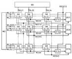
図1に示すPLDは、n個(n:2以上の整数)のロジックエレメントLE(ロジックエレメントLE21乃至ロジックエレメントLE2n)、n2個の回路SW(回路SW21−21乃至回路SW2n−2n)、ビットドライバBD、ワードドライバWDを有する。The PLD illustrated in FIG. 1 includes n (n: an integer equal to or greater than 2) logic elements LE (logic elements LE21 to LE2n), ntwo circuits SW (circuits SW21-21 to SW2n-2n), and bits. It has a driver BD and a word driver WD.
ロジックエレメントLEは、内部にコンフィギュレーションメモリを有し、当該コンフィギュレーションメモリに格納されたコンフィギュレーションデータに基づき、入力信号に対して特定の出力信号を出力する機能を有する。 The logic element LE has a configuration memory therein and has a function of outputting a specific output signal in response to an input signal based on configuration data stored in the configuration memory.
回路SWは、ロジックエレメントLE間の導通状態を制御する機能を有する。回路SWは、有している機能の性質上、「スイッチ」と表現することもできる。また、図1においては、n個のロジックエレメントLEに対し、n2個の回路SWを有する構成としているが、本発明はこれに限定されない。すなわち、1個のロジックエレメントLEそれぞれが自己を含めたn個のロジックエレメントLE全てと導通させる構成にする必要がないのであれば、n2個未満の回路SWを有する構成とすることもできる。例えば、1個のロジックエレメントLEそれぞれがm個(m:1以上かつn未満の整数)の回路SWと導通させることができればよいのであれば、m×n個の回路SWを有する構成とすることができる。The circuit SW has a function of controlling a conduction state between the logic elements LE. The circuit SW can also be expressed as a “switch” due to the nature of the functions it has. Although FIG. 1 shows a configuration in which n logic elements LE include n2 circuits SW, the present invention is not limited to this. That is, each one of the logic elements LE is if it is not necessary to configure to conduct the n-number of logic elements LE all, including self, it may be configured with n2 fewer than the circuit SW. For example, if it is only necessary that each of the one logic element LE can conduct with m (m: an integer of 1 or more and less than n) circuits, a configuration having m × n circuits SW is adopted. Can be.
ビットドライバBD、ワードドライバWDは、ロジックエレメントLE及び回路SWのコンフィギュレーションを制御する機能を有し、信号線WLにより選択されたコンフィギュレーションメモリに、信号線BL21乃至信号線BL2nの電位に応じたコンフィギュレーションデータを格納することができる。 The bit driver BD and the word driver WD have a function of controlling the configuration of the logic element LE and the circuit SW. The bit driver BD and the word driver WD store the configuration memory selected by the signal line WL in accordance with the potentials of the signal lines BL21 to BL2n. Configuration data can be stored.
図1に示す構成においては、回路SWは、2種類の信号線WLの一方により選択されたコンフィギュレーションメモリに、信号線BLの電位に応じたコンフィギュレーションデータを書き込むことにより、コンフィギュレーションを行なうことができる。例えば、回路SW21−22は、2種類の信号線WL(WL22[0]、WL22[1])により選択されたコンフィギュレーションメモリに、信号線BL21の電位に応じたコンフィギュレーションデータを書き込むことにより、コンフィギュレーションを行なうことができる。 In the configuration shown in FIG. 1, the circuit SW performs configuration by writing configuration data corresponding to the potential of the signal line BL to a configuration memory selected by one of the two types of signal lines WL. Can be. For example, the circuit SW21-22 writes configuration data corresponding to the potential of the signal line BL21 to the configuration memory selected by the two types of signal lines WL (WL22 [0], WL22 [1]). Configuration can be performed.
図2に回路SW21−22の回路構成を示す。なお、ここでは図1における回路SW21−22を代表例として説明するが、他の回路SWも同様に説明することができる。 FIG. 2 shows a circuit configuration of the circuits SW21-22. Here, the circuits SW21 to 22 in FIG. 1 will be described as a representative example, but other circuits SW can be similarly described.
回路SW21−22は、回路SW21−22a及び回路SW21−22bを有し、ロジックエレメントLE21及びロジックエレメントLE22間の導通状態を制御する機能(換言すれば、ロジックエレメントLE21及びロジックエレメントLE22間の導通または非導通を選択する機能)を有する。 The circuit SW21-22 includes a circuit SW21-22a and a circuit SW21-22b, and has a function of controlling a conduction state between the logic element LE21 and the logic element LE22 (in other words, a function of controlling conduction between the logic element LE21 and the logic element LE22. Function to select non-conduction).
回路SW21−22a(回路SW21−22b)は、トランジスタM21a(トランジスタM21b)、トランジスタM22a(トランジスタM22b)、トランジスタM23a(トランジスタM23b)、及び容量素子C21(容量素子C22)を有する。回路SW21−22a(回路SW21−22b)は、信号線WL22[0](信号線WL22[1])によりトランジスタM21a(トランジスタM21b)が導通状態となるとき、容量素子C21(容量素子C22)に信号線BL21に対応するコンフィギュレーションデータを書き込む。そして、ノードSN21(ノードSN22)に格納されたコンフィギュレーションデータに応じて、トランジスタM22a(トランジスタM22b)の導通、非導通が制御される。また、信号CONTEXT[0](信号CONTEXT[1])により、トランジスタM23a(トランジスタM23b)の導通、非導通を制御することで、回路SW21−22a(回路SW21−22b)は、ロジックエレメントLE21及びロジックエレメントLE22間の導通状態を制御することができる。また、トランジスタM22a(トランジスタM22b)のソースまたはドレインの一方は、ノードND21Oの電位を与える配線を介してロジックエレメントLE21と電気的に接続され、トランジスタM23a(トランジスタM23b)のソースまたはドレインの一方はノードND22Iの電位を与える配線を介してロジックエレメントLE22と電気的に接続されている。 The circuit SW21-22a (the circuit SW21-22b) includes the transistor M21a (the transistor M21b), the transistor M22a (the transistor M22b), the transistor M23a (the transistor M23b), and the capacitor C21 (the capacitor C22). The circuit SW21-22a (circuit SW21-22b) supplies a signal to the capacitor C21 (capacitor C22) when the transistor M21a (transistor M21b) is turned on by the signal line WL22 [0] (signal line WL22 [1]). The configuration data corresponding to the line BL21 is written. Then, conduction or non-conduction of the transistor M22a (transistor M22b) is controlled according to the configuration data stored in the node SN21 (node SN22). Further, by controlling the conduction or non-conduction of the transistor M23a (transistor M23b) by the signal CONTEXT [0] (signal CONTEXT [1]), the circuit SW21-22a (circuit SW21-22b) causes the logic element LE21 and the logic The conduction state between the elements LE22 can be controlled. One of a source and a drain of the transistor M22a (the transistor M22b) is electrically connected to the logic element LE21 through a wiring which supplies a potential of the node ND210, and one of a source and a drain of the transistor M23a (the transistor M23b) is a node. It is electrically connected to the logic element LE22 via a wiring for giving the potential of ND22I.
なお、回路SWは、ノードSN21及びノードSN22の電位を保持することで、コンフィギュレーションメモリとして振る舞うことができる。このため、トランジスタM21a及びトランジスタM21bとして、オフ電流が極めて小さいトランジスタを用いるのが好ましい。具体的には、チャネル形成領域に酸化物半導体を有するトランジスタを用いることが好ましい。 Note that the circuit SW can operate as a configuration memory by holding the potentials of the nodes SN21 and SN22. Therefore, it is preferable to use transistors with extremely low off-state current as the transistors M21a and M21b. Specifically, a transistor including an oxide semiconductor in a channel formation region is preferably used.
図3にロジックエレメントLE21の回路構成を示す。なお、ここでは図1におけるロジックエレメントLE21を代表例として説明するが、他のロジックエレメントLEも同様に説明することができる。 FIG. 3 shows a circuit configuration of the logic element LE21. Here, the logic element LE21 in FIG. 1 will be described as a representative example, but the other logic elements LE can be similarly described.
ロジックエレメントLE21は、ルックアップテーブル201(以下、本明細書において「LUT」と呼ぶことがある。)、記憶装置202、レジスタ203(以下、本明細書において「REGISTER」と呼ぶことがある。)、AND回路204(論理積回路)を有する。 The logic element LE21 includes a look-up table 201 (hereinafter, sometimes referred to as “LUT” in this specification), a
ルックアップテーブル201は、記憶装置202に設定された真理値表に基づき、配線を介して入力される4つの信号(dataA、dataB、dataC、dataD)に応じた特定の値を出力する機能を有する。なお、ルックアップテーブル201が4つの信号に応じた特定の出力値を出力する機能を有するとしてここでは説明したが、必ずしもこの構成には限定されない。すなわち、ルックアップテーブル201に入力される信号の数は4個のみに限定されるものではなく、k個(k:1以上の整数)でもよい。また、真理値表は、信号CONTEXT[0]または信号CONTEXT[1]を記憶装置202に入力することにより、自由に設定することができる。 The lookup table 201 has a function of outputting a specific value according to four signals (dataA, dataB, dataC, and dataD) input via wiring based on a truth table set in the
レジスタ203は、ルックアップテーブル201からの出力値を保持する機能を有する。また、レジスタ203で保持する値は、クロック信号CLK2に同期して変化する。AND回路204は、レジスタ203の出力と、配線を介して入力される信号SWITCHとの論理積を出力する機能を有する。すなわち、信号SWITCHが”L”レベルであるとき、AND回路204の出力は、レジスタ203の出力に依存せず、”L”レベルの電位となる。また、信号SWITCHが”H”レベルであるとき、AND回路204の出力は、レジスタ203の出力値がそのまま出力される。このように、信号SWITCHを”L”レベルとすることにより、ロジックエレメントLE21の出力を強制的に”L”レベルとすることができる。 The
回路SW21−22は、ロジックエレメントLE21及びロジックエレメントLE22間の導通状態を制御する機能を有する。そして、回路SW21−22は、ロジックエレメントLE21からの入力された信号を受けるとともに、ロジックエレメントLE22に信号を出力する機能を有する。また、回路SW21−22は、配線を介して信号CONTEXT[0]及び信号CONTEXT[1]が入力される構成を有しており、信号CONTEXT[0]及び信号CONTEXT[1]を制御することにより、第一のコンフィギュレーションデータセットに基づく回路構成(回路SW21−22a)と、第二のコンフィギュレーションデータセットに基づく回路構成(回路SW21−22b)とを瞬時に変更することができる。 The circuits SW21-22 have a function of controlling conduction between the logic elements LE21 and LE22. The circuit SW21-22 has a function of receiving a signal input from the logic element LE21 and outputting a signal to the logic element LE22. Further, the circuit SW21-22 has a configuration in which the signal CONTEXT [0] and the signal CONTEXT [1] are input via wiring, and controls the signal CONTEXT [0] and the signal CONTEXT [1] by controlling the signal CONTEXT [0] and the signal CONTEXT [1]. The circuit configuration based on the first configuration data set (circuit SW21-22a) and the circuit configuration based on the second configuration data set (circuit SW21-22b) can be instantaneously changed.
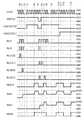
図4に図1乃至図3に示す回路のタイミングチャートを示す。 FIG. 4 shows a timing chart of the circuits shown in FIGS.
なお、図4に示すタイミングチャートは、図2における回路SW21−22aに第一のコンフィギュレーションデータセットのコンフィギュレーションを行い、その後第一のコンフィギュレーションデータセットに基づく回路構成により、半導体装置(チップ)が動作している最中に、図2における回路SW21−22bに第二のコンフィギュレーションデータセットの動的再構成を行なう場合を想定したものである。しかしながら、回路SW21−22aと回路SW21−22bは同一の構成を有しているので、逆の場合も同様に動作させることができる。 In the timing chart shown in FIG. 4, the first configuration data set is configured in the circuits SW21-22a in FIG. 2, and then the semiconductor device (chip) is configured by a circuit configuration based on the first configuration data set. 2 is assumed to be dynamically reconfigured in the second configuration data set in the circuits SW21-22b in FIG. However, since the circuits SW21-22a and SW21-22b have the same configuration, the same operation can be performed in the opposite case.
図4において、時刻T0から時刻T3の間に、第一のコンフィギュレーションデータセットに対して初期のコンフィギュレーションを行なう。まず、時刻T0から時刻T1の間、すなわち回路SW21−22への入力信号に相当するノードND21Oの電位(ロジックエレメントLE21と、トランジスタM22a(M22b)のソースまたはドレインの一方とを電気的に接続する配線の電位)が”L”レベルの間に、信号線WL21[0]に”H”レベルの信号を与え、信号線BL21に”H”レベルの信号を与えることで、回路SW21−21aに対して好条件のコンフィギュレーションが行われる。次に、時刻T1から時刻T2の間、すなわち、ノードND21Oの電位が”L”レベルの間に、信号線WL22[0]に”H”レベルの信号を与え、信号線BL21に”H”レベルの信号を与えることで、容量素子C21に”H”レベルに相当するコンフィギュレーションデータを書き込む。その後、信号線WL22[0]に”L”レベルの信号を、信号線BL21に”L”レベルの信号を与え、トランジスタM21aを非導通とすることで、ノードSN21のコンフィギュレーションデータを格納する。従って、回路SW21−22aに対して好条件のコンフィギュレーションが行われる。最後に、時刻T2から時刻T3の間で、残りのコンフィギュレーションメモリに、所望のコンフィギュレーションデータを書き込む。 In FIG. 4, an initial configuration is performed on the first configuration data set between time T0 and time T3. First, between the time T0 and the time T1, that is, the potential of the node ND210 corresponding to the input signal to the circuit SW21-22 (the logic element LE21 is electrically connected to one of the source and the drain of the transistor M22a (M22b)). When the potential of the wiring) is at the “L” level, an “H” level signal is applied to the signal line WL21 [0] and an “H” level signal is applied to the signal line BL21, whereby the circuit SW21-21a is supplied to the circuit SW21-21a. Configuration under favorable conditions. Next, an “H” level signal is applied to the signal line WL22 [0] during a period from the time T1 to the time T2, that is, while the potential of the node ND210 is “L” level, and an “H” level is applied to the signal line BL21. , The configuration data corresponding to the “H” level is written to the capacitive element C21. After that, an “L” level signal is supplied to the signal line WL22 [0] and an “L” level signal is supplied to the signal line BL21, so that the transistor M21a is turned off, so that the configuration data of the node SN21 is stored. Therefore, configuration under favorable conditions is performed on the circuits SW21-22a. Finally, the desired configuration data is written to the remaining configuration memory between time T2 and time T3.
時刻T3にて、信号CONTEXT[0]を”H”レベルにすることで、トランジスタM23aは導通する。時刻T4にて、ノードND21Oが”L”レベルの電位から”H”レベルの電位に変化すると、トランジスタM22aのゲート容量を介した容量結合により、ノードSN21の電位は昇圧される。従って、ノードND22Iの電位は速やかに”H”レベルとなる。すなわち、回路SW21−22を介した、ロジックエレメントLE21及びロジックエレメントLE22間の信号伝達速度は向上する。 At a time T3, the signal CONTEXT [0] is set to the “H” level, so that the transistor M23a is turned on. At the time T4, when the potential of the node ND21O changes from the “L” level potential to the “H” level potential, the potential of the node SN21 is boosted by capacitive coupling via the gate capacitance of the transistor M22a. Therefore, the potential of the node ND22I quickly becomes the “H” level. That is, the signal transmission speed between the logic elements LE21 and LE22 via the circuits SW21-22 is improved.
次に、時刻T5から時刻T9の間に、第二のコンフィギュレーションデータセットの動的再構成を行なう。まず、時刻T5にて、レジスタ203に入力されるクロック信号CLK2の供給を止める。その後、AND回路204に入力される信号SWITCHを”L”レベルとすることにより、ロジックエレメントLE21の出力(ノードND21Iの電位)を強制的に”L”レベルとする。次に、信号線WL22[1]を”H”レベルとして、信号線BL21を介してノードSN22に”H”レベルの信号を書き込む。時刻T5から時刻T6の間において、このような駆動方法を用いることで、回路SW21−22bに好条件のコンフィギュレーションを行うことができる。なお、回路SWに対して好条件のコンフィギュレーションを行うタイミングは、回路SW21−22bだけでなく、第二のコンフィギュレーションデータセットに対応する全ての回路SW(すなわち、回路SW21−21b乃至回路SW2n−2nbの全部でn2個ある回路SW)に対して同時に行っている。このため、第二のコンフィギュレーションデータセットに対応する全ての回路SWに対して正しいコンフィギュレーションデータを書き込む期間(時刻T6から時刻T9の間)に比較して、極めて短い時間で好条件のコンフィギュレーションを行うことができる。Next, the dynamic reconfiguration of the second configuration data set is performed between time T5 and time T9. First, at time T5, the supply of the clock signal CLK2 input to the
ここで、時刻T5から時刻T6の期間において、ノードND21Oの電位を強制的に”L”レベルとすることで、回路SW21−22の出力先であるロジックエレメントLE22のデータが変わってしまうことが懸念されるようにみえるが、本実施の形態では、レジスタ203に入力されるクロック信号CLK2の供給を止めることにより、時刻T5から時刻T6の期間中、ロジックエレメントLE22のデータが変わらないようにしている。このため、データの変動により、ロジックエレメントLE22が意図しない論理演算を行うこと(ロジックエレメントLE22の誤動作)を防止できる。 Here, during the period from time T5 to time T6, by forcibly setting the potential of the node ND21O to the “L” level, there is a concern that the data of the logic element LE22 that is the output destination of the circuit SW21-22 may change. However, in this embodiment, the supply of the clock signal CLK2 input to the
次に、時刻T6から時刻T9の間に、第二のコンフィギュレーションデータセットに対応する全ての回路SWに対して、正しいコンフィギュレーションデータを書き込む。まず、時刻T6から時刻T7の期間中においては、信号線WL21[1]に”H”レベルの信号を与え、信号線BL21乃至信号線BL2nを介して回路SW21−21b乃至回路SW2n−21bのコンフィギュレーションメモリに正しいコンフィギュレーションデータを書き込む。例えば、図4においては、回路SW21−21bのコンフィギュレーションメモリに”H”レベルの信号が、回路SW22−21bのコンフィギュレーションメモリに”L”レベルの信号が格納される。 Next, between time T6 and time T9, correct configuration data is written to all circuits SW corresponding to the second configuration data set. First, during a period from time T6 to time T7, an “H” level signal is supplied to the signal line WL21 [1], and the configuration of the circuits SW21-21b to SW2n-21b is performed via the signal lines BL21 to BL2n. Write the correct configuration data to the configuration memory. For example, in FIG. 4, an "H" level signal is stored in the configuration memory of the circuit SW21-21b, and an "L" level signal is stored in the configuration memory of the circuit SW22-21b.
時刻T7から時刻T8の期間中においては、信号線WL22[1]に”H”レベルの信号を与え、信号線BL21乃至信号線BL2nを介して回路SW21−22b乃至回路SW2n−22bのコンフィギュレーションメモリに正しいコンフィギュレーションデータを書き込む。例えば、図4においては、回路SW21−22bのコンフィギュレーションメモリに”H”レベルの信号が、回路SW22−22bのコンフィギュレーションメモリに”L”レベルの信号が格納される。 During the period from the time T7 to the time T8, an “H” level signal is supplied to the signal line WL22 [1], and the configuration memories of the circuits SW21-22b to SW2n-22b are transmitted through the signal lines BL21 to BL2n. Write the correct configuration data to For example, in FIG. 4, an "H" level signal is stored in the configuration memory of the circuit SW21-22b, and an "L" level signal is stored in the configuration memory of the circuit SW22-22b.
ここで回路SW21−22bに着目すると、時刻T7から時刻T8の間、すなわち、ノードND21Oの電位が”H”レベルのときに、信号線WL22[1]に”H”レベルの信号が、信号線BL21に”H”レベルの信号が与えられている。すなわち、悪条件のコンフィギュレーションが行われている。しかしながら、本実施の形態においては、時刻T5から時刻T6の間に、好条件のコンフィギュレーションを行ない、ノードSN22の電位は、VDDとなっている。そして、時刻T6から時刻T7の間で、ノードND21Oの電位が”L”レベルから”H”レベルに切り替わる際に、トランジスタM22bのゲート容量を介した容量結合により、ノードSN22の電位が例えば2VDD程度まで昇圧されている。すなわち、時刻T7から時刻T8の間において、トランジスタM21bは、信号線WL22[1]を介してゲートに”H”レベルの信号が、信号線BL21を介してソースに”H”レベルの信号が与えられている。したがって、ゲート−ソース間電圧が0Vとなり、トランジスタM21bは非導通となり、ノードSN21の電位は昇圧された電位(例えば2VDD程度の電位)を維持することができる。この結果、回路SW21−22bを介した信号伝達速度は向上した状態を維持し、回路SW21−22bの動作遅延を抑制することができる。 Here, focusing on the circuit SW21-22b, between the time T7 and the time T8, that is, when the potential of the node ND210 is at the “H” level, the signal of the “H” level is applied to the signal line WL22 [1]. An “H” level signal is given to BL21. That is, the configuration under the bad condition is performed. However, in the present embodiment, the configuration under favorable conditions is performed between the time T5 and the time T6, and the potential of the node SN22 is VDD. Then, when the potential of the node ND21O switches from the “L” level to the “H” level between the time T6 and the time T7, the potential of the node SN22 becomes, for example, about 2VDD due to capacitive coupling via the gate capacitance of the transistor M22b. It has been boosted up. That is, between the time T7 and the time T8, the transistor M21b applies an “H” level signal to the gate via the signal line WL22 [1] and an “H” level signal to the source via the signal line BL21. Have been. Therefore, the voltage between the gate and the source becomes 0 V, the transistor M21b is turned off, and the potential of the node SN21 can be maintained at a boosted potential (for example, a potential of about 2VDD). As a result, the signal transmission speed via the circuits SW21-22b is maintained in an improved state, and the operation delay of the circuits SW21-22b can be suppressed.
時刻T8から時刻T9の期間においては、時刻T6から時刻T7の期間、及び時刻T7から時刻T8の期間と同様にして、残りのコンフィギュレーションメモリに所望のコンフィギュレーションデータを書き込む。 During the period from time T8 to time T9, desired configuration data is written to the remaining configuration memory in the same manner as the period from time T6 to time T7 and the period from time T7 to time T8.
次に、時刻T10から時刻T11の間に、選択するコンフィギュレーションデータセットを入れ替える。すなわち、時刻T10において、信号CONTEXT[0]を”L”レベルとし、信号CONTEXT[1]を”H”レベルとすることにより、第二のコンフィギュレーションデータセットが選択される。 Next, the configuration data set to be selected is exchanged between time T10 and time T11. That is, at time T10, the signal CONTEXT [0] is set to the “L” level and the signal CONTEXT [1] is set to the “H” level, whereby the second configuration data set is selected.
時刻T12に、ノードND21Oを”H”レベルの電位から”L”レベルの電位へ変化させる。このとき、トランジスタM22bのゲート容量を介した容量結合により、ノードSN22の電位はVDDまで降圧されるが、トランジスタM22bのゲート・ソース間電圧はVDDであるため、ノードND22Iの電位は速やかに”L”レベルとなる。 At the time T12, the potential of the node ND210 is changed from the “H” level potential to the “L” level potential. At this time, the potential of the node SN22 drops to VDD due to capacitive coupling via the gate capacitance of the transistor M22b. However, since the gate-source voltage of the transistor M22b is VDD, the potential of the node ND22I quickly becomes “L”. "Level.
時刻T13に、ノードND21Oを”L”レベルの電位から”H”レベルの電位へ変化させる。このとき、トランジスタM22bのゲート容量を介した容量結合により、ノードSN22の電位は昇圧される。従って、ノードND22Iの電位は速やかに”H”レベルとなる。すなわち、回路SW21−22bを介したノードND21OとノードND22I間の信号伝達速度は向上する。 At the time T13, the potential of the node ND210 is changed from the “L” level potential to the “H” level potential. At this time, the potential of the node SN22 is boosted by capacitive coupling via the gate capacitance of the transistor M22b. Therefore, the potential of the node ND22I quickly becomes the “H” level. That is, the signal transmission speed between the nodes ND21O and ND22I via the circuits SW21-22b is improved.
以上説明したように、本実施の形態で説明した半導体装置の駆動方法は、第1のコンフィギュレーションメモリに保持されたコンフィギュレーションデータに基づく回路構成により半導体装置(チップ)が動作している最中に、第2のコンフィギュレーションメモリの動的再構成を行なう場合において、第2のコンフィギュレーションメモリに正しいコンフィギュレーションデータを書き込む期間とは別に、全ての第2のコンフィギュレーションメモリに好条件のコンフィギュレーションを行う期間(好条件のコンフィギュレーションデータを書き込む期間)を設けている点に特徴を有する。このような駆動方法を採用することにより、正しいコンフィギュレーションデータを書き込む条件に依らず、回路SWの動作速度の遅延を抑制できる。 As described above, in the method for driving a semiconductor device described in this embodiment, the semiconductor device (chip) is operating with a circuit configuration based on the configuration data held in the first configuration memory. In addition, when performing dynamic reconfiguration of the second configuration memory, apart from the period in which correct configuration data is written to the second configuration memory, all the second configuration memories have favorable conditions. (A period for writing configuration data under favorable conditions). By employing such a driving method, it is possible to suppress a delay in the operation speed of the circuit SW regardless of a condition for writing correct configuration data.
(実施の形態2)
本発明の一態様に係る半導体装置及びその駆動方法について、図2、図3、図5乃至図7を用いて説明する。(Embodiment 2)
A semiconductor device according to one embodiment of the present invention and a method for driving the semiconductor device will be described with reference to FIGS.
本実施の形態で説明する半導体装置の駆動方法は、好条件のコンフィギュレーションを行う期間を設けるという点において実施の形態1で説明した駆動方法と共通しているが、好条件のコンフィギュレーションを行う際に考慮しなければならないロジックエレメントLEのデータの変動による誤動作を防止する方法に関して相違しているので、特にこの点について詳細に説明する。 The driving method of a semiconductor device described in this embodiment is common to the driving method described in
図5に、本発明の一態様におけるPLDの回路構成を示す。 FIG. 5 illustrates a circuit configuration of a PLD according to one embodiment of the present invention.
図5に示す回路は、図1に示す回路と比較して、回路ST21乃至回路ST2n(n:2以上の整数)を有している点で相違するが、その他の構成は図1に示す回路と共通の回路を有しているので、共通部分については説明を省略する。 The circuit shown in FIG. 5 is different from the circuit shown in FIG. 1 in that it has circuits ST21 to ST2n (n: an integer of 2 or more), but other configurations are the same as those shown in FIG. Therefore, the description of the common part is omitted.
回路ST2nは、回路SW21−2n乃至回路SW2n−2nと、ロジックエレメントLE2nとの間に設けられている。すなわち、回路ST2nは、回路SW21−2n乃至回路SW2n−2nと電気的に接続されているとともに、ロジックエレメントLE2nと電気的に接続されている。また、回路ST2nは、回路SW21−2n乃至回路SW2n−2nから出力された信号が入力され、ロジックエレメントLE2nに信号を出力することができる機能を有する。また、回路ST2nは、回路SW21−2n乃至回路SW2n−2nから出力された信号(データ)を保持することができる機能を有する。 The circuit ST2n is provided between the circuits SW21-2n to SW2n-2n and the logic element LE2n. That is, the circuit ST2n is electrically connected to the circuits SW21-2n to SW2n-2n, and is also electrically connected to the logic element LE2n. The circuit ST2n has a function of receiving signals output from the circuits SW21-2n to SW2n-2n and outputting a signal to the logic element LE2n. Further, the circuit ST2n has a function of holding signals (data) output from the circuits SW21-2n to SW2n-2n.
図6に、本発明の一態様における回路ST22の具体的な回路構成の一例を示す。 FIG. 6 illustrates an example of a specific circuit configuration of the circuit ST22 in one embodiment of the present invention.
回路ST22は、トランジスタM24と、インバータ21と、を有する。そして、トランジスタM24のソースまたはドレインの一方は、回路SW21−22、及びインバータ21の入力端子と電気的に接続され、トランジスタM24のソースまたはドレインの他方は、配線と電気的に接続され、トランジスタM24のゲートは、インバータ21の出力端子と電気的に接続され、インバータ21の入力端子は、ロジックエレメントLE22と電気的に接続されている。また、トランジスタM24のソースまたはドレインの他方と電気的に接続されている配線には、基準電位よりも高い電位(高電位、またはVDD)が与えられている。なお、ノードND22Iには、回路SW22−22乃至回路SW2n−22も接続しているが、図6では省略している。 The circuit ST22 has a transistor M24 and an
図7に図2、図3、図5、図6に示す回路のタイミングチャートを示す。 FIG. 7 shows a timing chart of the circuits shown in FIGS. 2, 3, 5, and 6.
なお、図7に示すタイミングチャートは、実施の形態1と同様に、図2における回路SW21−22aに第一のコンフィギュレーションデータセットのコンフィギュレーションを行い、その後第一のコンフィギュレーションデータセットに基づく回路構成により、半導体装置(チップ)が動作している最中に、図2における回路SW21−22bに第二のコンフィギュレーションデータセットの動的再構成を行なう場合を想定したものである。 Note that the timing chart shown in FIG. 7 shows that the circuit SW21-22a in FIG. 2 performs the configuration of the first configuration data set and then performs the circuit based on the first configuration data set, as in the first embodiment. With this configuration, it is assumed that dynamic reconfiguration of the second configuration data set is performed in the circuits SW21-22b in FIG. 2 while the semiconductor device (chip) is operating.
図7に示すタイミングチャート、実施の形態1で説明した図4に示すタイミングチャートと比較すると、時刻T5から時刻T6の期間中の動作が相違しているが、その他の期間においては同様であるため、ここでは時刻T5から時刻T6の期間中の動作についてのみ説明し、その他の期間の動作については、実施の形態1における説明を援用する。 Compared with the timing chart shown in FIG. 7 and the timing chart shown in FIG. 4 described in
時刻T5から時刻T6の期間は、全ての回路SWに対して好条件のコンフィギュレーションを行う期間に相当する。まず、時刻T5にて、信号CONTEXT[0]を”L”レベルとして、トランジスタM23aを非導通状態(オフ状態)とする。その後、図3に示すAND回路204に入力される信号SWITCHを”L”レベルとすることにより、ロジックエレメントLE21の出力(ノードND21Iの電位)を強制的に”L”レベルとする。次に、信号線WL22[1]を”H”レベルとして、信号線BL21を介してノードSN22に”H”レベルの信号を書き込む。 The period from the time T5 to the time T6 corresponds to a period during which the configuration under favorable conditions is performed for all the circuits SW. First, at a time T5, the signal CONTEXT [0] is set to the “L” level, so that the transistor M23a is turned off (off). Thereafter, the signal SWITCH input to the AND
本実施の形態においては、回路SW21−22aの出力先にST22を有しているため、トランジスタM23aを非導通状態(オフ状態)としても、回路SW21−22aの出力データを保持することができる。したがって、ノードND21Oの電位が強制的に”L”レベルとなっている期間を有する時刻T5から時刻T6の期間中においても、ロジックエレメントLE22が意図しない論理演算を行うこと(ロジックエレメントLE22の誤動作)を防止できる。 In this embodiment, since the output destination of the circuit SW21-22a is the ST22, the output data of the circuit SW21-22a can be held even when the transistor M23a is turned off (off state). Therefore, even during the period from time T5 to time T6 having the period in which the potential of the node ND21O is forcibly at the “L” level, the logic element LE22 performs an unintended logical operation (malfunction of the logic element LE22). Can be prevented.
次に、時刻T6にて、信号CONTEXT[0]を”H”レベルとした後、全ての回路STに対して、正しいコンフィギュレーションデータを書き込んでいく。時刻T6以降の動作については、実施の形態1での説明を援用する。 Next, at time T6, after the signal CONTEXT [0] is set to the “H” level, correct configuration data is written to all the circuits ST. For the operation after the time T6, the description in
以上説明したように、本実施の形態で説明した半導体装置の駆動方法は、好条件のコンフィギュレーションを行う期間において、信号CONTEXT[0]を”L”レベルとするとともに、回路SW21−22の出力先とロジックエレメントLE22との間に回路ST22を設けているため、ロジックエレメントLE22が意図しない論理演算を行うこと(ロジックエレメントLE22の誤動作)を防止できる。 As described above, in the method for driving the semiconductor device described in this embodiment, the signal CONTEXT [0] is set to the “L” level and the output of the circuits SW21 to 22 during the period in which the configuration under favorable conditions is performed. Since the circuit ST22 is provided between the logic element LE22 and the logic element LE22, it is possible to prevent the logic element LE22 from performing an unintended logical operation (malfunction of the logic element LE22).
(実施の形態3)
本発明の一態様に係る半導体装置及びその駆動方法について、図13乃至図16を用いて説明する。(Embodiment 3)
A semiconductor device according to one embodiment of the present invention and a method for driving the semiconductor device will be described with reference to FIGS.
図13に、本発明の一態様における半導体装置の回路構成を示す。 FIG. 13 illustrates a circuit configuration of a semiconductor device according to one embodiment of the present invention.
図13に示すPLDは、n個(n:2以上の整数)のロジックエレメントLE(ロジックエレメントLE31乃至ロジックエレメントLE3n)、n2個の回路SW(回路SW31−31乃至回路SW3n−3n)、ビットドライバBD、ワードドライバWD、及びn個の回路ST(回路ST31乃至回路ST3n)を有する。The PLD illustrated in FIG. 13 includes n (n: an integer equal to or greater than 2) logic elements LE (logic elements LE31 to LE3n), ntwo circuits SW (circuits SW31-31 to SW3n-3n), and bits. It includes a driver BD, a word driver WD, and n circuits ST (circuits ST31 to ST3n).
ロジックエレメントLEは、内部にコンフィギュレーションメモリを有し、当該コンフィギュレーションメモリに格納されたコンフィギュレーションデータに基づき、入力信号に対して特定の出力信号を出力する機能を有する。 The logic element LE has a configuration memory therein and has a function of outputting a specific output signal in response to an input signal based on configuration data stored in the configuration memory.
回路SWは、ロジックエレメントLE間の導通状態を制御する機能を有する。回路SWは、有している機能の性質上、「スイッチ」と表現することもできる。また、図13においては、n個のロジックエレメントLEに対し、n2個の回路SWを有する構成としているが、本発明はこれに限定されない。すなわち、1個のロジックエレメントLEそれぞれが自己を含めたn個のロジックエレメントLE全てと導通させる構成にする必要がないのであれば、n2個未満の回路SWを有する構成とすることもできる。例えば、1個のロジックエレメントLEそれぞれがm個(m:1以上かつn未満の整数)の回路SWと導通させることができればよいのであれば、m×n個の回路SWを有する構成とすることができる。The circuit SW has a function of controlling a conduction state between the logic elements LE. The circuit SW can also be expressed as a “switch” due to the nature of the functions it has. Although FIG. 13 illustrates a configuration in which n logic elements LE include n2 circuits SW, the present invention is not limited to this. That is, each one of the logic elements LE is if it is not necessary to configure to conduct the n-number of logic elements LE all, including self, it may be configured with n2 fewer than the circuit SW. For example, if it is only necessary that each of the one logic element LE can conduct with m (m: an integer of 1 or more and less than n) circuits, a configuration having m × n circuits SW is adopted. Can be.
ビットドライバBD、ワードドライバWDは、ロジックエレメントLE及び回路SWのコンフィギュレーションを制御する機能を有し、信号線WLにより選択されたコンフィギュレーションメモリに、信号線BL31乃至信号線BL3nの電位に応じたコンフィギュレーションデータを格納することができる。 The bit driver BD and the word driver WD have a function of controlling the configuration of the logic element LE and the circuit SW, and store the configuration in the configuration memory selected by the signal line WL in accordance with the potentials of the signal lines BL31 to BL3n. Configuration data can be stored.
回路STは、ノードND31I乃至ノードND3nIの電位を強制的に”L”レベルとすることができる機能を有する。すなわち、回路STは、2つのロジックエレメント間の導通状態を非接続とすることができる機能を有する。回路STは、このような機能を有している性質上、「リセット回路」と表現することもできる。 The circuit ST has a function of forcibly setting the potentials of the nodes ND31I to ND3nI to “L” level. That is, the circuit ST has a function capable of disconnecting the conduction state between the two logic elements. The circuit ST can also be expressed as a “reset circuit” because of the property having such a function.
図13に示す構成においては、回路SWは、2種類の信号線WLの一方により選択されたコンフィギュレーションメモリに、信号線BLの電位に応じたコンフィギュレーションデータを書き込むことにより、コンフィギュレーションを行なうことができる。例えば、回路SW31−32は、2種類の信号線WL(WL32[0]、WL32[1])により選択されたコンフィギュレーションメモリに、信号線BL31の電位に応じたコンフィギュレーションデータを書き込むことにより、コンフィギュレーションを行なうことができる。 In the configuration shown in FIG. 13, the circuit SW performs configuration by writing configuration data corresponding to the potential of the signal line BL to a configuration memory selected by one of the two types of signal lines WL. Can be. For example, the circuits SW31-32 write configuration data corresponding to the potential of the signal line BL31 to the configuration memory selected by the two types of signal lines WL (WL32 [0] and WL32 [1]). Configuration can be performed.
図14に回路SW31−32の回路構成を示す。なお、ここでは図13における回路SW31−32を代表例として説明するが、他の回路SWも同様に説明することができる。 FIG. 14 shows the circuit configuration of the circuits SW31-SW32. Here, the circuits SW31-32 in FIG. 13 will be described as a representative example, but the other circuits SW can be similarly described.
回路SW31−32は、回路SW31−32a及び回路SW31−32bを有し、ロジックエレメントLE31及び回路ST32間の導通状態を制御する機能(換言すれば、ロジックエレメントLE31及び回路ST32間の導通または非導通を選択する機能)を有する。 The circuits SW31-32 include circuits SW31-32a and circuits SW31-32b, and have a function of controlling the conduction state between the logic element LE31 and the circuit ST32 (in other words, the conduction or non-conduction between the logic element LE31 and the circuit ST32). Function to select the
回路SW31−32a(回路SW31−32b)はトランジスタM31a(トランジスタM31b)、トランジスタM32a(トランジスタM32b)、トランジスタM33a(トランジスタM33b)、及び容量素子C31(容量素子C32)を有する。回路SW31−32a(回路SW31−32b)は、信号線WL32[0](WL32[1])によりトランジスタM31a(トランジスタM31b)が導通状態となるとき、容量素子C31(容量素子C32)に信号線BL31に対応するコンフィギュレーションデータを書き込む。そして、ノードSN31(ノードSN32)に格納されたコンフィギュレーションデータに応じて、トランジスタM32a(トランジスタM32b)の導通、非導通が制御される。また、トランジスタM32a(トランジスタM32b)のソースまたはドレインの一方は、ノードND32I(配線)を介して回路ST32と電気的に接続され、回路ST32は、ロジックエレメントLE32と電気的に接続され、トランジスタM32a(トランジスタM32b)のソースまたはドレインの他方は、トランジスタM33a(トランジスタM33b)のソースまたはドレインの一方と電気的に接続され、トランジスタM33a(トランジスタM33b)のソースまたはドレインの他方は、ノードND31O(配線)を介してロジックエレメントLE31と電気的に接続されている。また、配線を介してゲートに与えられる信号CONTEXT[0](信号CONTEXT[1])によってトランジスタM33a(トランジスタM33b)の導通、非導通を制御することで、回路SW31−32a(回路SW31−32b)は、ロジックエレメントLE31及び回路ST32間の導通状態を制御することができる。 The circuit SW31-32a (circuit SW31-32b) includes a transistor M31a (transistor M31b), a transistor M32a (transistor M32b), a transistor M33a (transistor M33b), and a capacitor C31 (capacitor C32). When the transistor M31a (transistor M31b) is turned on by the signal line WL32 [0] (WL32 [1]), the circuit SW31-32a (circuit SW31-32b) connects the signal line BL31 to the capacitor C31 (capacitor C32). Write the configuration data corresponding to. Then, conduction or non-conduction of the transistor M32a (transistor M32b) is controlled according to the configuration data stored in the node SN31 (node SN32). One of a source and a drain of the transistor M32a (transistor M32b) is electrically connected to the circuit ST32 through a node ND32I (wiring). The circuit ST32 is electrically connected to the logic element LE32, and is connected to the transistor M32a ( The other of the source and the drain of the transistor M32b) is electrically connected to one of the source and the drain of the transistor M33a (the transistor M33b). The other of the source and the drain of the transistor M33a (the transistor M33b) is connected to the node ND31O (wiring). It is electrically connected to the logic element LE31 via the power supply. In addition, by controlling conduction / non-conduction of the transistor M33a (transistor M33b) by a signal CONTEXT [0] (signal CONTEXT [1]) given to a gate via a wiring, the circuits SW31 to 32a (circuits SW31 to 32b) are controlled. Can control the conduction state between the logic element LE31 and the circuit ST32.
なお、回路SWは、ノードSN31及びノードSN32の電位を保持することで、コンフィギュレーションメモリとして振る舞うことができる。このため、トランジスタM31a及びトランジスタM31bとして、オフ電流が極めて小さいトランジスタを用いるのが好ましい。具体的には、チャネル形成領域に酸化物半導体を有するトランジスタを用いることが好ましい。 Note that the circuit SW can operate as a configuration memory by holding the potentials of the nodes SN31 and SN32. Therefore, it is preferable to use transistors with extremely low off-state current as the transistors M31a and M31b. Specifically, a transistor including an oxide semiconductor in a channel formation region is preferably used.
図15に回路ST32の回路構成を示す。なお、ここでは図13における回路ST32を代表例として説明するが、他の回路STも同様に説明することができる。 FIG. 15 shows a circuit configuration of the circuit ST32. Here, the circuit ST32 in FIG. 13 is described as a representative example, but the other circuits ST can be similarly described.
回路ST32は、トランジスタM34、トランジスタM35、トランジスタM36、及びインバータINV31を有する。また、回路ST32は、ノードND32Iの電位を”H”レベルで安定させる、または”L”レベルにリセットする機能を有する。ここで、ノードND32Iの電位が”H”レベルの場合、インバータINV31及びトランジスタM35を介して、ノードND32Iには”H”レベルの電位に相当するVDDが供給されるため、”H”レベルの電位を保持(安定)させることができる。また、ノードND32Iの電位を強制的に”L”レベルとしたいときは、信号線RESET3に”H”レベルの電位を与えてトランジスタM34を導通させることで、ノードND32Iの電位を強制的に”L”レベルとさせることができる。また、信号線LEkeepに”L”レベルの電位を与えてトランジスタM36を非導通とさせることで、ロジックエレメントLE32内部のデータが変化することを抑制できる。 The circuit ST32 includes a transistor M34, a transistor M35, a transistor M36, and an inverter INV31. The circuit ST32 has a function of stabilizing the potential of the node ND32I at “H” level or resetting it to “L” level. Here, when the potential of the node ND32I is at the “H” level, VDD corresponding to the potential of the “H” level is supplied to the node ND32I via the inverter INV31 and the transistor M35. Can be held (stable). When the potential of the node ND32I is forcibly set to the “L” level, an “H” level potential is applied to the signal line RESET3 to turn on the transistor M34, thereby forcibly setting the potential of the node ND32I to the “L” level. "Level. Further, by applying an “L” level potential to the signal line LEkeep to make the transistor M36 non-conductive, a change in data inside the logic element LE32 can be suppressed.
図16に図13乃至図15に示す回路のタイミングチャートを示す。 FIG. 16 shows a timing chart of the circuits shown in FIGS.
なお、図16に示すタイミングチャートは、図14における回路SW31−32aに第一のコンフィギュレーションデータセットのコンフィギュレーションを行い、その後第一のコンフィギュレーションデータセットに基づく回路構成により、半導体装置(チップ)が動作している(アクティブとなっている)最中に、図14における回路SW31−32bに第二のコンフィギュレーションデータセットの動的再構成を行なう場合を想定したものである。しかしながら、回路SW31−32aと回路SW31−32bは同一の構成を有しているので、逆の場合も同様に動作させることができる。 In the timing chart shown in FIG. 16, the first configuration data set is configured in the circuits SW31 to 32a in FIG. 14, and then the semiconductor device (chip) is configured by a circuit configuration based on the first configuration data set. It is assumed that the dynamic reconfiguration of the second configuration data set is performed in the circuits SW31 to 32b in FIG. 14 while the is operating (active). However, since the circuits SW31-32a and SW31-32b have the same configuration, the same operation can be performed in the opposite case.
図16において、時刻T0から時刻T3の間に、第一のコンフィギュレーションデータセットに対して初期のコンフィギュレーションを行なう。まず、時刻T0から時刻T1の間、すなわち回路SW31−32の出力信号に相当するノードND32Iの電位(トランジスタM32a(M32b)のソースまたはドレインの一方と、回路ST32とを電気的に接続する配線の電位)が”L”レベルの間に、信号線WL31[0]に”H”レベルの信号を与え、信号線BL31に”H”レベルの信号を与えることで、回路SW31−31aに対して好条件のコンフィギュレーションが行われる。次に、時刻T1から時刻T2の間、すなわち、ノードND32Iの電位が”L”レベルの間に、信号線WL32[0]に”H”レベルの信号を与え、信号線BL31に”H”レベルの信号を与えることで、容量素子C31に”H”レベルに相当するコンフィギュレーションデータを書き込む。その後、信号線WL32[0]に”L”レベルの信号を、信号線BL31に”L”レベルの信号を与え、トランジスタM31aを非導通とすることで、ノードSN31のコンフィギュレーションデータを格納する。従って、回路SW31−32aに対して好条件のコンフィギュレーションが行われる。最後に、時刻T2から時刻T3の間で、残りのコンフィギュレーションメモリに、所望のコンフィギュレーションデータを書き込む。 In FIG. 16, an initial configuration is performed on the first configuration data set between time T0 and time T3. First, between the time T0 and the time T1, that is, the potential of the node ND32I corresponding to the output signal of the circuit SW31-32 (the potential of one of the source and the drain of the transistor M32a (M32b) and the wiring electrically connecting the circuit ST32). By supplying a signal at the “H” level to the signal line WL31 [0] and a signal at the “H” level to the signal line BL31 while the potential (potential) is at the “L” level, it is favorable for the circuits SW31 to 31a. The configuration of the condition is performed. Next, an “H” level signal is supplied to the signal line WL32 [0] during a period from time T1 to time T2, that is, while the potential of the node ND32I is at “L” level, and “H” level is applied to the signal line BL31. , The configuration data corresponding to the “H” level is written to the capacitive element C31. After that, an “L” level signal is applied to the signal line WL32 [0] and an “L” level signal is applied to the signal line BL31, so that the transistor M31a is turned off, so that the configuration data of the node SN31 is stored. Therefore, the configuration under favorable conditions is performed on the circuits SW31-32a. Finally, the desired configuration data is written to the remaining configuration memory between time T2 and time T3.
時刻T3にて、信号CONTEXT[0]の電位を”H”レベルにすることで、トランジスタM33aは導通する。時刻T4にて、ノードND31Oが”L”レベルの電位から”H”レベルの電位に変化すると、トランジスタM32aのゲート容量を介した容量結合により、ノードSN31の電位は昇圧される。従って、ノードND32Iの電位は速やかに”H”レベルとなる。すなわち、回路SW31−32を介した、ロジックエレメントLE31及びロジックエレメントLE32間の信号伝達速度は向上する。 At the time T3, the potential of the signal CONTEXT [0] is set to “H” level, so that the transistor M33a is turned on. At the time T4, when the potential of the node ND31O changes from the “L” level potential to the “H” level potential, the potential of the node SN31 is boosted by capacitive coupling via the gate capacitance of the transistor M32a. Therefore, the potential of the node ND32I quickly becomes the “H” level. That is, the signal transmission speed between the logic elements LE31 and LE32 via the circuits SW31-32 is improved.
次に、時刻T5から時刻T9の間に、第二のコンフィギュレーションデータセットの動的再構成を行なう。まず、時刻T5から時刻T6の間に、信号CONTEXT[0]を”L”レベルとする。また、信号線LEkeepの電位を”L”レベル、信号線RESET3の電位を”H”レベルとすることで、ノードND32Iの電位を強制的に”L”レベルとすることができる。次に、信号線WL32[1]を”H”レベルとして、信号線BL31を介してノードSN32に”H”レベルの信号を書き込む。このような駆動方法を用いることで、回路SW31−32bに好条件のコンフィギュレーションを行うことができる。なお、回路SWに対して好条件のコンフィギュレーションを行うタイミングは、回路SW31−32bだけでなく、第二のコンフィギュレーションデータセットに対応する全ての回路SW(すなわち、回路SW31−31b乃至回路SW3n−3nbの全部でn2個ある回路SW)に対して同時に行っている。このため、第二のコンフィギュレーションデータセットに対応する全ての回路SWに対して正しいコンフィギュレーションデータを書き込む期間(時刻T6から時刻T9の間)に比較して、極めて短い時間で好条件のコンフィギュレーションを行うことができる。Next, the dynamic reconfiguration of the second configuration data set is performed between time T5 and time T9. First, the signal CONTEXT [0] is set to the “L” level between the time T5 and the time T6. Further, by setting the potential of the signal line LEkeep to “L” level and the potential of the signal line RESET3 to “H” level, the potential of the node ND32I can be forcibly set to “L” level. Next, the signal line WL32 [1] is set to the “H” level, and an “H” level signal is written to the node SN32 via the signal line BL31. By using such a driving method, configuration under favorable conditions can be performed on the circuits SW31 to 32b. In addition, the timing of performing the favorable configuration for the circuit SW is not limited to the circuits SW31 to 32b, but also to all the circuits SW corresponding to the second configuration data set (that is, the circuits SW31 to 31b to SW3n-). This is performed simultaneously for all n2 circuits SW) of 3 nb. For this reason, compared to the period (from time T6 to time T9) in which correct configuration data is written to all the circuits SW corresponding to the second configuration data set, the configuration under favorable conditions is extremely short. It can be performed.
ここで、時刻T5から時刻T6の期間において、ノードND32Iの電位を強制的に”L”レベルとすることで、回路SW31−32の出力先であるロジックエレメントLE32のデータが変わってしまうことが懸念されるようにみえるが、本実施の形態では、信号線LEkeepの電位を”L”レベルとし、回路ST32におけるトランジスタM36を非導通とさせることで、時刻T5から時刻T6の期間中、ロジックエレメントLE32のデータが変わらないようにしている。このため、データの変動により、ロジックエレメントLE32が意図しない論理演算を行うこと(ロジックエレメントLE32の誤動作)を防止できる。 Here, during the period from the time T5 to the time T6, there is a concern that the data of the logic element LE32, which is the output destination of the circuit SW31-32, is changed by forcibly setting the potential of the node ND32I to the “L” level. In this embodiment, the potential of the signal line LEkeep is set to the “L” level, and the transistor M36 in the circuit ST32 is turned off, so that the logic element LE32 during the period from the time T5 to the time T6. Data is not changed. Therefore, it is possible to prevent the logic element LE32 from performing an unintended logical operation (malfunction of the logic element LE32) due to a change in data.
また、時刻T5から時刻T6の期間において、ノードND31Oの電位は”H”レベルであるため、ロジックエレメントLE31から、トランジスタM34を介して、貫通電流が流れることが危惧されるが、信号CONTEXT[0]を”L”レベルとすることで、全ての回路SWは非導通となり、過剰な電流が流れるのを抑制できる。その後、信号線RESET3の電位を”L”レベルとし、信号CONTEXT[0]及び、信号LEkeepを”H”レベルとすることで、ノードND32Iの電位を強制的に”L”レベルの電位としていたのを解除し、時刻T5における信号を再度読み込むことができる。 In the period from the time T5 to the time T6, the potential of the node ND31O is at the “H” level. Therefore, a through current may flow from the logic element LE31 via the transistor M34. However, the signal CONTEXT [0] Is set to the “L” level, all the circuits SW are turned off, and an excessive current can be suppressed from flowing. Thereafter, the potential of the signal line RESET3 is set to the “L” level, the signal CONTEXT [0] and the signal LEkeep are set to the “H” level, thereby forcibly setting the potential of the node ND32I to the “L” level. And the signal at time T5 can be read again.
次に、時刻T6から時刻T9の間に、第二のコンフィギュレーションデータセットに対応する全ての回路SWに対して、正しいコンフィギュレーションデータを書き込む。まず、時刻T6から時刻T7の期間中においては、信号線WL31[1]に”H”レベルの信号を与え、信号線BL31乃至信号線BL3nを介して回路SW31−31b乃至回路SW3n−31bのコンフィギュレーションメモリに正しいコンフィギュレーションデータを書き込む。例えば、図16においては、回路SW31−31bのコンフィギュレーションメモリに”H”レベルの信号が格納される。ここで、回路SW31−31bのコンフィギュレーションは、ノードND32Iの電位が”H”レベルの期間に行なわれているが、時刻T5から時刻T6の間に、好条件のコンフィギュレーションを行なっているため、回路SW31−31bを介した信号伝達速度は向上した状態を維持することができる。 Next, between time T6 and time T9, correct configuration data is written to all circuits SW corresponding to the second configuration data set. First, during a period from time T6 to time T7, an “H” level signal is supplied to the signal line WL31 [1], and the configuration of the circuits SW31-31b to SW3n-31b is performed via the signal lines BL31 to BL3n. Write the correct configuration data to the configuration memory. For example, in FIG. 16, an “H” level signal is stored in the configuration memory of the circuits SW31 to 31b. Here, the configuration of the circuits SW31 to 31b is performed during the period when the potential of the node ND32I is at the “H” level, but the configuration under favorable conditions is performed between the time T5 and the time T6. The signal transmission speed via the circuits SW31-31b can be maintained in an improved state.
時刻T7から時刻T8の期間中においては、信号線WL32[1]に”H”レベルの信号を与え、信号線BL31乃至信号線BL3nを介して回路SW31−32b乃至回路SW3n−32bのコンフィギュレーションメモリに正しいコンフィギュレーションデータを書き込む。例えば、図16においては、回路SW31−32bのコンフィギュレーションメモリに”H”レベルの信号が、回路SW32−32bのコンフィギュレーションメモリに”L”レベルの信号が格納される。ここで、回路SW31−32bのコンフィギュレーションメモリは、時刻T5から時刻T6の間に好条件のコンフィギュレーションが行なわれているため、コンフィギュレーションデータの変化は起こらない。 During the period from the time T7 to the time T8, an “H” level signal is supplied to the signal line WL32 [1], and the configuration memories of the circuits SW31-32b to SW3n-32b are transmitted through the signal lines BL31 to BL3n. Write the correct configuration data to For example, in FIG. 16, an "H" level signal is stored in the configuration memory of the circuits SW31-32b, and an "L" level signal is stored in the configuration memory of the circuits SW32-32b. Here, in the configuration memories of the circuits SW31 to 32b, since the configuration under favorable conditions is performed between the time T5 and the time T6, the configuration data does not change.
時刻T8から時刻T9の期間中においては、時刻T6から時刻T7の期間、及び時刻T7から時刻T8の期間と同様にして、残りのコンフィギュレーションメモリに所望のコンフィギュレーションデータを書き込む。以上のように、本実施の形態においては、時刻T5から時刻T6の間に、第二のコンフィギュレーションデータセットに対応する全ての回路SWにおいて好条件のコンフィギュレーションを行っているため、時刻T6から時刻T9の期間で、所望のコンフィギュレーションデータを書き込む際に、ノードND32Iの電位に依らず、信号伝達速度の低下を抑制することができる。 During the period from time T8 to time T9, desired configuration data is written to the remaining configuration memory in the same manner as the period from time T6 to time T7 and the period from time T7 to time T8. As described above, in the present embodiment, the configuration under favorable conditions is performed in all the circuits SW corresponding to the second configuration data set between the time T5 and the time T6. When desired configuration data is written in the period of time T9, a reduction in signal transmission speed can be suppressed regardless of the potential of the node ND32I.
次に、時刻T10から時刻T11の間に、選択するコンフィギュレーションデータセットを入れ替える。すなわち、時刻T10において、信号CONTEXT[0]を”L”レベルとし、信号CONTEXT[1]を”H”レベルとすることにより、第二のコンフィギュレーションデータセットが選択される。 Next, the configuration data set to be selected is exchanged between time T10 and time T11. That is, at time T10, the signal CONTEXT [0] is set to the “L” level and the signal CONTEXT [1] is set to the “H” level, whereby the second configuration data set is selected.
時刻T12に、ノードND31Oを”H”レベルの電位から”L”レベルの電位へ変化させる。このとき、トランジスタM32bのゲート容量を介した容量結合により、ノードSN32の電位はVDDまで降圧されるが、トランジスタM32bのゲート・ソース間電圧はVDDであるため、ノードND32Iの電位は速やかに”L”レベルとなる。 At the time T12, the potential of the node ND31O is changed from the “H” level potential to the “L” level potential. At this time, the potential of the node SN32 drops to VDD due to capacitive coupling via the gate capacitance of the transistor M32b. However, since the voltage between the gate and the source of the transistor M32b is VDD, the potential of the node ND32I quickly becomes “L”. "Level.
時刻T13に、ノードND31Oを”L”レベルの電位から”H”レベルの電位へ変化させる。このとき、トランジスタM32bのゲート容量を介した容量結合により、ノードSN32の電位は昇圧される。従って、ノードND32Iの電位は速やかに”H”レベルとなる。すなわち、回路SW31−32bを介したノードND31OとノードND32I間の信号伝達速度は向上する。 At the time T13, the potential of the node ND31O is changed from the “L” level potential to the “H” level potential. At this time, the potential of the node SN32 is boosted by capacitive coupling via the gate capacitance of the transistor M32b. Therefore, the potential of the node ND32I quickly becomes the “H” level. That is, the signal transmission speed between the nodes ND31O and ND32I via the circuits SW31-32b is improved.
以上説明したように、本実施の形態で説明した半導体装置の駆動方法は、第1のコンフィギュレーションメモリに保持されたコンフィギュレーションデータに基づく回路構成により半導体装置(チップ)が動作している最中に、第2のコンフィギュレーションメモリの動的再構成を行なう場合において、第2のコンフィギュレーションメモリに正しいコンフィギュレーションデータを書き込む期間とは別に、全ての第2のコンフィギュレーションメモリに好条件のコンフィギュレーションを行う期間(好条件のコンフィギュレーションデータを書き込む期間)を設けている点に特徴を有する。このような駆動方法を採用することにより、正しいコンフィギュレーションデータを書き込む条件に依らず、回路SWの動作速度の遅延を抑制できる。 As described above, in the method for driving a semiconductor device described in this embodiment, the semiconductor device (chip) is operating with a circuit configuration based on the configuration data held in the first configuration memory. In addition, when performing dynamic reconfiguration of the second configuration memory, apart from the period in which correct configuration data is written to the second configuration memory, all the second configuration memories have favorable conditions. (A period for writing configuration data under favorable conditions). By employing such a driving method, it is possible to suppress a delay in the operation speed of the circuit SW regardless of a condition for writing correct configuration data.
また、回路SWの動作速度の遅延の抑制を実現可能とする、新規の半導体装置を提供することができる。 Further, it is possible to provide a novel semiconductor device that can suppress a delay in the operation speed of the circuit SW.
(実施の形態4)
本実施の形態では、本発明の一態様の半導体装置の構成の一例について、図面を参照しながら説明する。(Embodiment 4)
In this embodiment, an example of a structure of a semiconductor device of one embodiment of the present invention will be described with reference to drawings.
図8に、図2で示した回路SW21−22の断面構造の一部を示す。図8におけるトランジスタ23の構造は、たとえば、図2におけるトランジスタM21a、トランジスタM21bに適用することができる。また、図8におけるトランジスタ22の構造は、たとえば、図2におけるトランジスタM22a、トランジスタM22bに適用することができる。 FIG. 8 shows a part of the cross-sectional structure of the circuit SW21-22 shown in FIG. The structure of the
図8において、破線A1−A2で示す領域では、トランジスタ22及びトランジスタ23のチャネル長方向における断面構造を示しており、破線A3−A4で示す領域では、トランジスタ22及びトランジスタ23のチャネル幅方向における断面構造を示している。ただし、本実施の形態では、トランジスタ22のチャネル長方向とトランジスタ23のチャネル長方向とが概略一致している構成(概略平行な構成)を示しているが、必ずしも一致していなくともよい。 8, a region indicated by a broken line A1-A2 shows a cross-sectional structure of the
ここで、トランジスタのチャネル長方向とは、ソース(ソース領域またはソース電極)及びドレイン(ドレイン領域またはドレイン電極)間において、キャリアが移動する方向を指し、チャネル幅方向は、基板と水平な面内において、チャネル長方向に対して垂直の方向を指すものとする。 Here, the channel length direction of a transistor refers to a direction in which carriers move between a source (a source region or a source electrode) and a drain (a drain region or a drain electrode), and the channel width direction is in a plane horizontal to the substrate. , The direction perpendicular to the channel length direction.
また、図8において、トランジスタ22はチャネル形成領域に酸化物半導体を含み、トランジスタ23はチャネル形成領域に単結晶の半導体を含む構成を示している。図8においては、基板400として単結晶の基板を用いることにより、トランジスタ23のチャネル形成領域に単結晶の半導体を含む構成としているが、絶縁層を介して単結晶の基板上に設けられた単結晶の半導体層(代表的には、SOI基板)にチャネル形成領域が設けられた構成とすることもできる。 8 illustrates a structure in which the
基板400は、例えば、シリコン基板、ゲルマニウム基板、シリコンゲルマニウム基板等を用いることができる。図8では、単結晶シリコン基板を基板400として用いる場合を例示している。 As the
トランジスタ23は、素子分離法により電気的に分離されている。素子分離法は、選択酸化法(LOCOS法:Local Oxidation of Silicon法)、トレンチ分離法(STI法:Shallow Trench Isolation)等を用いることができる。図8では、トレンチ分離法を用いてトランジスタ23を電気的に分離する場合を例示している。具体的に、図8では、エッチング等により基板400に形成されたトレンチに、酸化珪素などが含まれる絶縁物を埋め込んだ後、当該絶縁物をエッチング等により部分的に除去することで形成される素子分離領域401により、トランジスタ23を素子分離させている。 The
トレンチ以外の領域に存在する基板400の凸部には、トランジスタ23の不純物領域402及び不純物領域403と、不純物領域402及び不純物領域403に挟まれたチャネル形成領域404とが設けられている。さらに、トランジスタ23は、チャネル形成領域404を覆う絶縁膜405と、絶縁膜405を間に挟んでチャネル形成領域404と重なるゲート電極406とを有する。 An
トランジスタ23では、チャネル形成領域404における凸部の側部及び上部と、ゲート電極406とが絶縁膜405を間に挟んで重なることで、チャネル形成領域404の側部と上部を含めた広い範囲においてキャリアが流れる。そのため、基板400上におけるトランジスタ23の占有面積を小さく抑えつつ、トランジスタ23におけるキャリアの移動量を増加させることができる。その結果、トランジスタ23は、オン電流が大きくなると共に、電界効果移動度が高められる。特に、チャネル形成領域404における凸部のチャネル幅方向の長さ(チャネル幅)をW、チャネル形成領域404における凸部の膜厚をTとすると、チャネル幅Wに対する膜厚Tの比(アスペクト比)が高い場合、キャリアが流れる範囲はより広くなるため、トランジスタ23のオン電流をより大きくすることができ、電界効果移動度もより高められる。バルクの半導体基板を用いたトランジスタ23の場合、アスペクト比は0.5以上であることが望ましく、1以上であることがより望ましい。 In the
トランジスタ23の上方には、絶縁膜411が設けられている。絶縁膜411には開口部が設けられている。この開口部には、不純物領域402、不純物領域403とそれぞれ電気的に接続されている導電膜412、導電膜413と、ゲート電極406と電気的に接続されている導電膜414と、が設けられている。 An insulating
導電膜412は、絶縁膜411上に形成された導電膜416と電気的に接続されており、導電膜413は、絶縁膜411上に形成された導電膜417に電気的に接続されており、導電膜414は、絶縁膜411上に形成された導電膜418と電気的に接続されている。 The
導電膜416乃至導電膜418の上方には、絶縁膜420が設けられている。そして、絶縁膜420の上方には、酸素、水素、または水の拡散を防止する効果(ブロッキング効果)を有する絶縁膜421が設けられている。絶縁膜421は、密度が高くて緻密である程、また未結合手が少なく化学的に安定である程、より高いブロッキング効果を示す。酸素、水素、または水の拡散を防止する効果を有する絶縁膜としては、例えば、酸化アルミニウム、酸化窒化アルミニウム、酸化ガリウム、酸化窒化ガリウム、酸化イットリウム、酸化窒化イットリウム、酸化ハフニウム、酸化窒化ハフニウム等を用いることができる。また、水素、または水の拡散を防止する絶縁膜としては、例えば、窒化シリコン、窒化酸化シリコン等を用いることができる。 An insulating
絶縁膜421の上方には絶縁膜422が設けられており、絶縁膜422の上方には、トランジスタ22が設けられている。 An insulating
トランジスタ22は、絶縁膜422上に、酸化物半導体を含む半導体膜430と、半導体膜430と電気的に接続された導電膜432及び導電膜433と、半導体膜430を覆うゲート絶縁膜431と、ゲート絶縁膜431を間に挟んで半導体膜430と重なるゲート電極434と、を有する。ここで、導電膜432及び導電膜433は、ソース電極またはドレイン電極としての機能を有する。また、絶縁膜420乃至絶縁膜422には開口部が設けられており、この開口部において導電膜433は導電膜418と電気的に接続されている。 The
なお、図8においては、ゲート絶縁膜431を間に挟んで半導体膜430と重なるゲート電極434を有するトランジスタ22を示しているが、本発明はこの構成に限定されない。すなわち、トランジスタ22は、ゲート電極434を有するとともに、絶縁膜422を間に挟んで半導体膜430と重なるゲート電極をさらに有する構成(すなわち、一対のゲート電極を有する構成)とすることもできる。 Note that FIG. 8 illustrates the
トランジスタ22が一対のゲート電極を有している場合、一方のゲート電極には導通状態または非導通状態を制御するための信号が与えられ、他方のゲート電極には、電位が他の電極または配線から与えられる構成とすることもできる。この場合、一対のゲート電極に、同じ高さの電位が与えられていても良いし、他方のゲート電極にのみ接地電位などの固定の電位が与えられていても良い。他方のゲート電極に与える電位の高さを制御することで、トランジスタの閾値電圧を制御することができる。 In the case where the
また、図8では、トランジスタ22がゲート電極434に対応した一つのチャネル形成領域を有する構造(シングルゲート構造)を例示しているが、互いに電気的に接続された複数のゲート電極を有し、複数のチャネル形成領域を有する構造(マルチゲート構造)とすることもできる。 FIG. 8 illustrates the structure in which the
また、図8に示すように、トランジスタ22は、半導体膜430として、絶縁膜422上において酸化物半導体膜430a乃至酸化物半導体膜430cが順に積層された構造を例示しているが、半導体膜430として単層の酸化物半導体膜を有する構造とすることもできる。 As illustrated in FIG. 8, the
次に、酸化物半導体膜にチャネル形成領域を有するトランジスタ22の構成の一例について、図9を用いながら説明する。 Next, an example of a structure of the
図9(A)は、トランジスタ22の上面図を示したものである。なお、図9(A)では、トランジスタ22のレイアウトを明確にするために、各種の絶縁膜を省略している。また、図9(A)に示した上面図の、破線A1−A2における断面図を図9(B)に示し、破線A3−A4における断面図を図9(C)に示す。 FIG. 9A illustrates a top view of the
図9に示すように、トランジスタ22は、絶縁表面97に形成された絶縁膜91上において順に積層された酸化物半導体膜92a及び酸化物半導体膜92bと、酸化物半導体膜92bに電気的に接続され、ソース電極またはドレイン電極としての機能を有する導電膜93及び導電膜94と、酸化物半導体膜92b、導電膜93及び導電膜94上の酸化物半導体膜92cと、ゲート絶縁膜としての機能を有し、なおかつ酸化物半導体膜92c上に位置する絶縁膜95と、ゲート電極としての機能を有し、なおかつ絶縁膜95上において酸化物半導体膜92a乃至酸化物半導体膜92cと重なる導電膜96と、を有する。なお、絶縁表面97は、ガラス基板や半導体基板などの表面であってもよいし、ガラス基板や半導体基板上に半導体素子が形成された素子基板の表面であってもよい。 As shown in FIG. 9, the
次に、酸化物半導体膜にチャネル形成領域を有するトランジスタ22の構成の他の一例について、図10を用いながら説明する。 Next, another example of the structure of the
図10(A)は、トランジスタ22の上面図を示したものである。なお、図10(A)では、トランジスタ22のレイアウトを明確にするために、各種の絶縁膜を省略している。また、図10(A)に示した上面図の、破線A1−A2における断面図を図10(B)に示し、破線A3−A4における断面図を図10(C)に示す。 FIG. 10A is a top view of the
図10に示すように、トランジスタ22は、絶縁膜91上において順に積層された酸化物半導体膜92a乃至酸化物半導体膜92cと、酸化物半導体膜92cに電気的に接続され、ソース電極またはドレイン電極としての機能を有する導電膜93及び導電膜94と、ゲート絶縁膜としての機能を有し、なおかつ酸化物半導体膜92c、導電膜93及び導電膜94上に位置する絶縁膜95と、ゲート電極としての機能を有し、なおかつ絶縁膜95上において酸化物半導体膜92a乃至酸化物半導体膜92cと重なる導電膜96とを有する。 As illustrated in FIG. 10, the
このように、図9及び図10では、酸化物半導体膜92a乃至酸化物半導体膜92cという積層構造を有するトランジスタ22の構成を例示している。 9 and 10 illustrate the structure of the
酸化物半導体膜92a乃至酸化物半導体膜92cが順に積層されている半導体膜をトランジスタ22が有する場合、酸化物半導体膜92a及び酸化物半導体膜92cは、酸化物半導体膜92bを構成する金属元素の少なくとも1つを構成要素に含み、伝導帯下端のエネルギーが酸化物半導体膜92bよりも0.05eV以上、0.07eV以上、0.1eV以上または0.15eV以上、かつ2eV以下、1eV以下、0.5eV以下または0.4eV以下、真空準位に近い酸化物膜である。また、酸化物半導体膜92bは、少なくともインジウムを含むと、キャリア移動度が高くなるため好ましい。 In the case where the
上記構成の半導体膜をトランジスタ22が有する場合、ゲート電極に電圧を印加することで、半導体膜に電界が加わると、半導体膜のうち、伝導帯下端のエネルギーが小さい酸化物半導体膜92bにチャネル領域が形成される。即ち、酸化物半導体膜92bと絶縁膜95との間に酸化物半導体膜92cが設けられていることによって、絶縁膜95と離隔している酸化物半導体膜92bに、チャネル領域を形成することができる。 In the case where the
また、酸化物半導体膜92cは、酸化物半導体膜92bを構成する金属元素の少なくとも1つをその構成要素に含むため、酸化物半導体膜92bと酸化物半導体膜92cの界面では、界面散乱が起こりにくい。従って、当該界面においてキャリアの動きが阻害されにくく、トランジスタ22の電界効果移動度が高くなるという効果を奏する。 In addition, since the
また、酸化物半導体膜92bと酸化物半導体膜92aの界面に界面準位が形成されると、界面近傍の領域にもチャネル領域が形成されるために、トランジスタ22の閾値電圧が変動してしまう。しかし、酸化物半導体膜92aは、酸化物半導体膜92bを構成する金属元素の少なくとも1つをその構成要素に含むため、酸化物半導体膜92bと酸化物半導体膜92aの界面には、界面準位が形成されにくい。よって、上記構成により、トランジスタ22の閾値電圧等の電気的特性のばらつきを、低減することができる。 In addition, when an interface state is formed at the interface between the
また、酸化物半導体膜間に不純物が存在することによって、各膜の界面にキャリアの流れを阻害する界面準位が形成されることがないよう、複数の酸化物半導体膜を積層させることが望ましい。積層された酸化物半導体膜の膜間に不純物が存在していると、酸化物半導体膜間における伝導帯下端のエネルギーの連続性が失われ、界面近傍において、キャリアがトラップされるか、あるいは再結合により消滅してしまうからである。膜間における不純物を低減させることで、主成分である一の金属を少なくとも共に有する複数の酸化物半導体膜を、単に積層させるよりも、連続接合(ここでは特に伝導帯下端のエネルギーが各膜の間で連続的に変化するU字型の井戸構造を有している状態)が形成されやすくなる。 In addition, it is preferable that a plurality of oxide semiconductor films be stacked so that an interface state which inhibits carrier flow is not formed at an interface between the films due to the presence of impurities between the oxide semiconductor films. . When impurities exist between the stacked oxide semiconductor films, the continuity of energy at the bottom of the conduction band between the oxide semiconductor films is lost, and carriers are trapped or regenerated near the interface. This is because they disappear due to bonding. By reducing impurities between the films, a plurality of oxide semiconductor films each having at least one metal as a main component are continuously bonded (here, the energy at the bottom of the conduction band is particularly low in each film) rather than simply stacking. (A state having a U-shaped well structure that continuously changes between them) is easily formed.
連続接合を形成するためには、ロードロック室を備えたマルチチャンバー方式の成膜装置(スパッタリング装置)を用いて各膜を大気に触れさせることなく連続して積層することが必要となる。スパッタリング装置における各チャンバーは、酸化物半導体にとって不純物となる水等を可能な限り除去すべくクライオポンプのような吸着式の真空排気ポンプを用いて高真空排気(5×10⁻⁷Pa以上かつ1×10⁻⁴Pa以下の程度まで)とすることが好ましい。または、ターボ分子ポンプとコールドトラップを組み合わせて排気系からチャンバー内に気体が逆流しないようにしておくことが好ましい。In order to form a continuous junction, it is necessary to use a multi-chamber type film forming apparatus (sputtering apparatus) having a load lock chamber and to continuously stack the films without exposure to the atmosphere. Each chamber in the sputtering apparatus is evacuated to a high vacuum (5 × 10⁻⁷ Pa or higher and 1 × 10⁻⁷ Pa or higher) using an adsorption-type vacuum exhaust pump such as a cryopump in order to remove water and the like that are impurities in the oxide semiconductor as much as possible. × 10−4 Pa or less). Alternatively, it is preferable that a turbo molecular pump and a cold trap be combined so that gas does not flow backward from the exhaust system into the chamber.
高純度の真性な酸化物半導体を得るためには、各チャンバー内を高真空排気するのみならず、スパッタリングに用いるガスの高純度化も重要である。上記ガスとして用いる酸素ガスやアルゴンガスの露点を、−40℃以下、好ましくは−80℃以下、より好ましくは−100℃以下とし、使用するガスの高純度化を図ることで、酸化物半導体膜に水分等が取り込まれることを可能な限り防ぐことができる。具体的に、酸化物半導体膜92bがIn−M−Zn酸化物(Mは、Ga(ガリウム)、Y(イットリウム)、Zr(ジルコニウム)、La(ランタン)、Ce(セリウム)、またはNd(ネオジム)を表す)の場合、酸化物半導体膜92bを成膜するために用いるターゲットにおいて、金属元素の原子数比をIn:M:Zn=x1:y1:z1とすると、x1/y1は、1/3以上かつ6以下、さらには1以上かつ6以下であって、z1/y1は、1/3以上かつ6以下、さらには1以上かつ6以下であることが好ましい。なお、z1/y1を1以上かつ6以下とすることで、酸化物半導体膜92bとしてCAAC−OS膜が形成されやすくなる。ターゲットの金属元素の原子数比の代表例としては、In:M:Zn=1:1:1、In:M:Zn=3:1:2等がある。In order to obtain a high-purity intrinsic oxide semiconductor, it is important not only to evacuate each chamber to high vacuum but also to increase the purity of a gas used for sputtering. The dew point of oxygen gas or argon gas used as the above gas is set at -40 ° C or lower, preferably -80 ° C or lower, more preferably -100 ° C or lower, and the oxide semiconductor film is highly purified. It is possible to prevent moisture and the like from being taken into the device as much as possible. Specifically, the
具体的に、酸化物半導体膜92a、酸化物半導体膜92cがIn−M−Zn酸化物の場合、酸化物半導体膜92a、酸化物半導体膜92cを成膜するために用いるターゲットにおいて、金属元素の原子数比をIn:M:Zn=x2:y2:z2とすると、x2/y2<x1/y1であって、z2/y2は、1/3以上かつ6以下、さらには1以上かつs6以下であることが好ましい。なお、z2/y2を1以上かつ6以下とすることで、酸化物半導体膜92a、酸化物半導体膜92cとしてCAAC−OS膜が形成されやすくなる。ターゲットの金属元素の原子数比の代表例としては、In:M:Zn=1:3:2、In:M:Zn=1:3:4、In:M:Zn=1:3:6、In:M:Zn=1:3:8等がある。Specifically, in the case where the
なお、酸化物半導体膜92a及び酸化物半導体膜92cの厚さは、3nm以上かつ100nm以下、好ましくは3nm以上かつ50nm以下とする。また、酸化物半導体膜92bの厚さは、3nm以上かつ200nm以下、好ましくは3nm以上かつ100nm以下であり、さらに好ましくは3nm以上かつ50nm以下である。 Note that the thickness of the
3層構造の半導体膜において、酸化物半導体膜92a乃至酸化物半導体膜92cは、非晶質または結晶質の両方の形態を取りうる。ただし、チャネル領域が形成される酸化物半導体膜92bが結晶質であることにより、トランジスタ22に安定した電気的特性を付与することができるため、酸化物半導体膜92bは結晶質であることが好ましい。 In the three-layer semiconductor film, each of the
なお、チャネル形成領域とは、トランジスタ22の半導体膜のうち、ゲート電極と重なり、かつソース電極とドレイン電極に挟まれる領域を意味する。また、チャネル領域とは、チャネル形成領域において、電流が主として流れる領域をいう。 Note that a channel formation region refers to a region of the semiconductor film of the
例えば、酸化物半導体膜92a及び酸化物半導体膜92cとして、スパッタリング法により形成したIn−Ga−Zn酸化物膜を用いる場合、酸化物半導体膜92a及び酸化物半導体膜92cの成膜には、In−Ga−Zn酸化物(In:Ga:Zn=1:3:2[原子数比])であるターゲットを用いることができる。成膜条件は、例えば、成膜ガスとしてアルゴンガスを30sccm、酸素ガスを15sccm用い、圧力0.4Paとし、基板温度を200℃とし、DC電力0.5kWとすればよい。 For example, when an In—Ga—Zn oxide film formed by a sputtering method is used as the
また、酸化物半導体膜92bをCAAC−OS膜とする場合、酸化物半導体膜92bの成膜には、In−Ga−Zn酸化物(In:Ga:Zn=1:1:1[原子数比])を含む多結晶ターゲットを用いることが好ましい。成膜条件は、例えば、成膜ガスとしてアルゴンガスを30sccm、酸素ガスを15sccm用い、圧力を0.4Paとし、基板の温度300℃とし、DC電力0.5kWとすることができる。 In the case where the
なお、酸化物半導体膜92a乃至92cは、スパッタリング法により形成することができるが、他の方法、例えば、熱CVD法により形成してもよい。熱CVD法の例としてMOCVD(Metal Organic Chemical Vapor Deposition)法やALD(Atomic Layer Deposition)法を使っても良い。 Note that the
なお、電子供与体(ドナー)となる水分または水素などの不純物が低減され、なおかつ酸素欠損が低減されることにより高純度化された酸化物半導体(purified Oxide Semiconductor)は、キャリア発生源が少ないため、i型(真性半導体)又はi型に限りなく近くすることができる。そのため、高純度化された酸化物半導体膜にチャネル形成領域を有するトランジスタは、オフ電流が著しく小さく、信頼性が高い。そして、当該酸化物半導体膜にチャネル形成領域が形成されるトランジスタは、閾値電圧がプラスとなる電気的特性(ノーマリーオフ特性ともいう。)になりやすい。 Note that an oxide semiconductor (purified oxide semiconductor) which is reduced in impurities such as moisture or hydrogen serving as an electron donor and has reduced oxygen vacancies has a small number of carrier generation sources. , I-type (intrinsic semiconductor) or i-type. Therefore, a transistor including a channel formation region in a highly purified oxide semiconductor film has extremely low off-state current and high reliability. Then, a transistor in which a channel formation region is formed in the oxide semiconductor film tends to have positive threshold voltage (also referred to as normally-off characteristics).
具体的に、高純度化された酸化物半導体膜にチャネル形成領域を有するトランジスタのオフ電流が小さいことは、様々な実験により証明できる。例えば、チャネル幅が1×106μmでチャネル長が10μmの素子であっても、ソース電極とドレイン電極間の電圧(ドレイン電圧)が1Vから10Vの範囲において、オフ電流が、半導体パラメータアナライザの測定限界以下、すなわち1×10⁻¹³A以下という特性を得ることができる。この場合、トランジスタのチャネル幅で規格化したオフ電流は、100zA/μm以下であることが分かる。また、容量素子とトランジスタとを接続して、容量素子に流入または容量素子から流出する電荷を当該トランジスタで制御する回路を用いて、オフ電流の測定を行った。当該測定では、高純度化された酸化物半導体膜を上記トランジスタのチャネル形成領域に用い、容量素子の単位時間あたりの電荷量の推移から当該トランジスタのオフ電流を測定した。その結果、トランジスタのソース電極とドレイン電極間の電圧が3Vの場合に、数十yA/μmという、さらに小さいオフ電流が得られることが分かった。従って、高純度化された酸化物半導体膜をチャネル形成領域に用いたトランジスタは、オフ電流が、シリコンを用いたトランジスタに比べて著しく小さい。Specifically, various experiments can prove low off-state current of a transistor including a channel formation region in a highly purified oxide semiconductor film. For example, even in an element having a channel width of 1 × 106 μm and a channel length of 10 μm, when the voltage (drain voltage) between the source electrode and the drain electrode is in the range of 1 V to 10 V, the off-state current of the semiconductor parameter analyzer A characteristic of less than the measurement limit, that is, 1 × 10⁻¹³ A or less can be obtained. In this case, the off-state current normalized by the channel width of the transistor is 100 zA / μm or less. In addition, off-state current was measured using a circuit in which a capacitor and a transistor were connected and charge flowing into or out of the capacitor was controlled by the transistor. In the measurement, a highly purified oxide semiconductor film was used for a channel formation region of the transistor, and the off-state current of the transistor was measured from a change in the amount of charge of the capacitor per unit time. As a result, it was found that when the voltage between the source electrode and the drain electrode of the transistor was 3 V, an even smaller off-state current of several tens of yA / μm was obtained. Therefore, a transistor including a highly purified oxide semiconductor film for a channel formation region has significantly lower off-state current than a transistor including silicon.
また、高純度化された酸化物半導体膜を用いたトランジスタは、−25℃から150℃までの極めて広い温度範囲において、オフ電流の変動がほとんどないという特徴を有する。このように、高純度化された酸化物半導体膜を用いたトランジスタは、シリコンを用いたトランジスタと比較して、オフ電流が著しく小さく、かつ温度依存性が極めて小さいという有利な効果を奏する。本発明の一態様においては、このような特徴を有するトランジスタを図2に示すトランジスタM21aやトランジスタM21bに用いているため、コンフィギュレーションメモリを極めて広い温度範囲において不揮発性とすることができる。 Further, a transistor including a highly purified oxide semiconductor film has a feature in that there is almost no change in off-state current in an extremely wide temperature range from -25 ° C to 150 ° C. Thus, a transistor including a highly purified oxide semiconductor film has an advantageous effect of significantly lower off-state current and extremely low temperature dependence, as compared with a transistor including silicon. In one embodiment of the present invention, a transistor having such characteristics is used for the transistor M21a and the transistor M21b illustrated in FIG. 2, so that the configuration memory can be nonvolatile over an extremely wide temperature range.
なお、本明細書において高純度化された酸化物半導体膜とは、真性フェルミレベルとの差が0.5eVより小さいフェルミレベルを有することをいう。この場合、酸化物半導体膜のキャリア密度は、1×10¹⁷/cm3未満(好ましくは、1×1015/cm3未満、より好ましくは1×1013/cm3未満)である。Note that in this specification, a highly purified oxide semiconductor film has a Fermi level whose difference from an intrinsic Fermi level is smaller than 0.5 eV. In this case, the carrier density of the oxide semiconductor film is lower than 1 × 10¹⁷ / cm3 (preferably, lower than 1 × 10¹⁵ / cm3 , more preferably, lower than 1 × 10¹³ / cm3 ).
また、半導体膜として酸化物半導体膜を用いる場合、少なくともインジウム(In)または亜鉛(Zn)を含むことが好ましい。また、これに加えて、酸化物半導体を用いたトランジスタの電気的特性のばらつきを減らすためのスタビライザーとして、ガリウム(Ga)、スズ(Sn)、ハフニウム(Hf)、アルミニウム(Al)、もしくはジルコニウム(Zr)から選ばれた1種または複数種の元素を含むことが好ましい。 In the case where an oxide semiconductor film is used as the semiconductor film, it is preferable that the oxide semiconductor film contain at least indium (In) or zinc (Zn). In addition, as a stabilizer for reducing variation in electric characteristics of a transistor including an oxide semiconductor, gallium (Ga), tin (Sn), hafnium (Hf), aluminum (Al), or zirconium ( It preferably contains one or more elements selected from Zr).
酸化物半導体の中でもIn−Ga−Zn酸化物、In−Sn−Zn酸化物などは、炭化シリコン、窒化ガリウム、または酸化ガリウムとは異なり、スパッタリング法や湿式法により電気的特性の優れたトランジスタを作製することが可能であり、量産性に優れるといった利点がある。また、炭化シリコン、窒化ガリウム、または酸化ガリウムとは異なり、上記In−Ga−Zn酸化物は、ガラス基板上に、電気的特性の優れたトランジスタを作製することが可能である。また、基板の大型化にも対応が可能である。 Among oxide semiconductors, In-Ga-Zn oxide, In-Sn-Zn oxide, and the like, unlike silicon carbide, gallium nitride, or gallium oxide, have a transistor with excellent electrical characteristics by a sputtering method or a wet method. It can be manufactured, and has an advantage of excellent mass productivity. Further, unlike silicon carbide, gallium nitride, or gallium oxide, the above In—Ga—Zn oxide enables a transistor with excellent electric characteristics to be manufactured over a glass substrate. Further, it is possible to cope with an increase in the size of the substrate.
また、他のスタビライザーとして、ランタノイドである、ランタン(La)、セリウム(Ce)、プラセオジム(Pr)、ネオジム(Nd)、サマリウム(Sm)、ユウロピウム(Eu)、ガドリニウム(Gd)、テルビウム(Tb)、ジスプロシウム(Dy)、ホルミウム(Ho)、エルビウム(Er)、ツリウム(Tm)、イッテルビウム(Yb)、ルテチウム(Lu)のいずれか一種または複数種を含んでいてもよい。 Other stabilizers include lanthanoids such as lanthanum (La), cerium (Ce), praseodymium (Pr), neodymium (Nd), samarium (Sm), europium (Eu), gadolinium (Gd), and terbium (Tb). , Dysprosium (Dy), holmium (Ho), erbium (Er), thulium (Tm), ytterbium (Yb), and lutetium (Lu).
例えば、酸化物半導体として、酸化インジウム、酸化ガリウム、酸化スズ、酸化亜鉛、In−Zn酸化物、Sn−Zn酸化物、Al−Zn酸化物、Zn−Mg酸化物、Sn−Mg酸化物、In−Mg酸化物、In−Ga酸化物、In−Ga−Zn酸化物(IGZOとも表記する)、In−Al−Zn酸化物、In−Sn−Zn酸化物、Sn−Ga−Zn酸化物、Al−Ga−Zn酸化物、Sn−Al−Zn酸化物、In−Hf−Zn酸化物、In−La−Zn酸化物、In−Pr−Zn酸化物、In−Nd−Zn酸化物、In−Ce−Zn酸化物、In−Sm−Zn酸化物、In−Eu−Zn酸化物、In−Gd−Zn酸化物、In−Tb−Zn酸化物、In−Dy−Zn酸化物、In−Ho−Zn酸化物、In−Er−Zn酸化物、In−Tm−Zn酸化物、In−Yb−Zn酸化物、In−Lu−Zn酸化物、In−Sn−Ga−Zn酸化物、In−Hf−Ga−Zn酸化物、In−Al−Ga−Zn酸化物、In−Sn−Al−Zn酸化物、In−Sn−Hf−Zn酸化物、In−Hf−Al−Zn酸化物を用いることができる。 For example, as an oxide semiconductor, indium oxide, gallium oxide, tin oxide, zinc oxide, In—Zn oxide, Sn—Zn oxide, Al—Zn oxide, Zn—Mg oxide, Sn—Mg oxide, In -Mg oxide, In-Ga oxide, In-Ga-Zn oxide (also referred to as IGZO), In-Al-Zn oxide, In-Sn-Zn oxide, Sn-Ga-Zn oxide, Al -Ga-Zn oxide, Sn-Al-Zn oxide, In-Hf-Zn oxide, In-La-Zn oxide, In-Pr-Zn oxide, In-Nd-Zn oxide, In-Ce -Zn oxide, In-Sm-Zn oxide, In-Eu-Zn oxide, In-Gd-Zn oxide, In-Tb-Zn oxide, In-Dy-Zn oxide, In-Ho-Zn Oxide, In-Er-Zn oxide, In- m-Zn oxide, In-Yb-Zn oxide, In-Lu-Zn oxide, In-Sn-Ga-Zn oxide, In-Hf-Ga-Zn oxide, In-Al-Ga-Zn oxide , An In-Sn-Al-Zn oxide, an In-Sn-Hf-Zn oxide, or an In-Hf-Al-Zn oxide can be used.
なお、例えば、In−Ga−Zn酸化物とは、InとGaとZnを含む酸化物という意味であり、InとGaとZnの比率は問わない。また、InとGaとZn以外の金属元素を含んでいてもよい。In−Ga−Zn酸化物は、無電界時の抵抗が十分に高くオフ電流を十分に小さくすることが可能であり、また、移動度も高い。 Note that, for example, an In—Ga—Zn oxide means an oxide containing In, Ga, and Zn, and there is no limitation on the ratio of In: Ga: Zn. Further, a metal element other than In, Ga, and Zn may be included. The In-Ga-Zn oxide has sufficiently high resistance in the absence of an electric field, can have sufficiently low off-state current, and has high mobility.
例えば、In−Sn−Zn酸化物では比較的容易に高い移動度が得られる。しかしながら、In−Ga−Zn酸化物でも、バルク内欠陥密度を低減することにより移動度を上げることができる。 For example, high mobility can be obtained relatively easily with an In—Sn—Zn oxide. However, even with an In—Ga—Zn oxide, mobility can be increased by reducing the defect density in the bulk.
また、トランジスタ22において、ソース電極及びドレイン電極に用いられる導電性材料によっては、ソース電極及びドレイン電極中の金属が、酸化物半導体膜から酸素を引き抜くことがある。この場合、酸化物半導体膜のうち、ソース電極及びドレイン電極に接する領域が、酸素欠損の形成によりn型化される。n型化された領域は、ソース領域またはドレイン領域として機能するため、酸化物半導体膜とソース電極及びドレイン電極との間におけるコンタクト抵抗を下げることができる。よって、n型化された領域が形成されることで、トランジスタ22の移動度及びオン電流を高めることができ、それにより、トランジスタ22を用いた半導体装置の高速動作を実現することができる。 In the
高速動作が実現する酸化物半導体膜を有するトランジスタは、図8のトランジスタ23として使用することができる。このようにトランジスタ23も酸化物半導体膜を有する場合、トランジスタ23は、トランジスタ22と同層に形成するとよい。すなわち、共通の出発膜を酸化物半導体層として、エッチングしたものを用いて、トランジスタ22と、トランジスタ23を構成することができる。なお酸化物半導体膜を有するトランジスタ23上に、酸化物半導体膜を有するトランジスタ22を形成する場合、集積度を高めることができる。 A transistor including an oxide semiconductor film which achieves high-speed operation can be used as the
また本発明の一態様は、信号伝達速度を向上させることができるため、n型化された領域を有さない酸化物半導体膜を有するトランジスタであっても、図8のトランジスタ23に適用することができる。 In addition, one embodiment of the present invention can improve the signal transmission speed; therefore, even when a transistor including an oxide semiconductor film without an n-type region is used as the
なお、ソース電極及びドレイン電極中の金属による酸素の引き抜きは、ソース電極及びドレイン電極をスパッタリング法などにより形成する際に起こりうるし、ソース電極及びドレイン電極を形成した後に行われる加熱処理によっても起こりうる。また、n型化される領域は、酸素と結合し易い導電性材料をソース電極及びドレイン電極に用いることで、より形成されやすくなる。上記導電性材料としては、例えば、アルミニウム(Al)、クロム(Cr)、銅(Cu)、タンタル(Ta)、チタン(Ti)、モリブデン(Mo)、タングステン(W)などが挙げられる。 Note that oxygen can be extracted by a metal in the source electrode and the drain electrode when the source electrode and the drain electrode are formed by a sputtering method or the like, or can be generated by heat treatment performed after the source electrode and the drain electrode are formed. . The n-type region is more easily formed by using a conductive material which is easily bonded to oxygen for the source electrode and the drain electrode. Examples of the conductive material include aluminum (Al), chromium (Cr), copper (Cu), tantalum (Ta), titanium (Ti), molybdenum (Mo), and tungsten (W).
複数の積層された酸化物半導体膜を有する半導体膜をトランジスタ22に用いる場合、n型化される領域は、チャネル領域となる酸化物半導体膜92bにまで達していることが、トランジスタ22の移動度及びオン電流を高め、半導体装置の高速動作を実現する上で好ましい。 In the case where a semiconductor film including a plurality of stacked oxide semiconductor films is used for the
絶縁膜91は、加熱により上記酸素の一部を酸化物半導体膜92a乃至酸化物半導体膜92cに供給する機能を有する絶縁膜であることが望ましい。また、絶縁膜91は、欠陥が少ないことが好ましく、代表的には、ESR測定により得られる、シリコンのダングリングボンドに由来するg=2.001を持つスピンの密度が1×10¹⁸spins/cm3以下であることが好ましい。The insulating
絶縁膜91は、加熱により上記酸素の一部を酸化物半導体膜92a乃至酸化物半導体膜92cに供給する機能を有するため、酸化物であることが望ましく、例えば、酸化アルミニウム、酸化マグネシウム、酸化珪素、酸化窒化珪素、窒化酸化珪素、酸化ガリウム、酸化ゲルマニウム、酸化イットリウム、酸化ジルコニウム、酸化ランタン、酸化ネオジム、酸化ハフニウムおよび酸化タンタルなどを用いることができる。絶縁膜91は、プラズマCVD(Chemical Vapor Deposition)法またはスパッタリング法等により、形成することができる。 The insulating
なお、本明細書中において、酸化窒化物は、その組成として、窒素よりも酸素の含有量が多い材料を指し、窒化酸化物は、その組成として、酸素よりも窒素の含有量が多い材料を指す。 Note that in this specification, oxynitride refers to a material having a higher oxygen content than nitrogen as its composition, and nitrided oxide refers to a material having a higher nitrogen content than oxygen as its composition. Point.
なお、図9及び図10に示すトランジスタ22は、チャネル領域が形成される酸化物半導体膜92bの端部のうち、導電膜93及び導電膜94とは重ならない端部、言い換えると、導電膜93及び導電膜94が位置する領域とは異なる領域に位置する端部と、導電膜96とが、重なる構成を有する。酸化物半導体膜92bの端部は、当該端部を形成するためのエッチングでプラズマに曝されるときに、エッチングガスから生じた塩素ラジカル、フッ素ラジカル等が、酸化物半導体を構成する金属元素と結合しやすい。よって、酸化物半導体膜の端部では、当該金属元素と結合していた酸素が脱離しやすい状態にあるため、酸素欠損が形成され、n型化しやすいやすいと考えられる。しかし、図9及び図10に示すトランジスタ22では、導電膜93及び導電膜94とは重ならない酸化物半導体膜92bの端部と、導電膜96とが重なるため、導電膜96の電位を制御することにより、当該端部にかかる電界を制御することができる。よって、酸化物半導体膜92bの端部を介して導電膜93と導電膜94の間に流れる電流を、導電膜96に与える電位によって制御することができる。本明細書においては、このようなトランジスタ22の構造を、Surrounded Channel(S−Channel)構造とよぶ。 Note that in the
具体的に、S−Channel構造の場合、トランジスタ22がオフとなるような電位を導電膜96に与えたときは、当該端部を介して導電膜93と導電膜94の間に流れるオフ電流を小さく抑えることができる。そのため、トランジスタ22では、大きなオン電流を得るためにチャネル長を短くし、その結果、酸化物半導体膜92bの端部における導電膜93と導電膜94の間の長さが短くなっても、トランジスタ22のオフ電流を小さく抑えることができる。よって、トランジスタ22は、チャネル長を短くすることで、オンのときには大きいオン電流を得ることができ、オフのときにはオフ電流を小さく抑えることができる。 Specifically, in the case of the S-Channel structure, when a potential at which the
また、具体的に、S−Channel構造の場合、トランジスタ22がオンとなるような電位を導電膜96に与えたときは、当該端部を介して導電膜93と導電膜94の間に流れる電流を大きくすることができる。当該電流は、トランジスタ22の電界効果移動度とオン電流の増大に寄与する。そして、酸化物半導体膜92bの端部と、導電膜96とが重なることで、酸化物半導体膜92bにおいてキャリアの流れる領域が、絶縁膜95に近い酸化物半導体膜92bの界面近傍のみでなく、酸化物半導体膜92bの広い範囲においてキャリアが流れるため、トランジスタ22におけるキャリアの移動量が増加する。この結果、トランジスタ22のオン電流が大きくなる共に、電界効果移動度が高くなり、代表的には電界効果移動度が10cm2/V・s以上、さらには20cm2/V・s以上となる。なお、ここでの電界効果移動度は、酸化物半導体膜の物性値としての移動度の近似値ではなく、トランジスタの飽和領域における電流駆動力の指標であり、見かけ上の電界効果移動度である。Specifically, in the case of the S-Channel structure, when a potential that turns on the
以下では、酸化物半導体膜の構造について説明する。 The structure of the oxide semiconductor film is described below.
本明細書において、「平行」とは、二つの直線が−10°以上10°以下の角度で配置されている状態をいう。従って、−5°以上5°以下の場合も含まれる。また、「略平行」とは、二つの直線が−30°以上30°以下の角度で配置されている状態をいう。また、「垂直」とは、二つの直線が80°以上100°以下の角度で配置されている状態をいう。従って、85°以上95°以下の場合も含まれる。また、「略垂直」とは、二つの直線が60°以上120°以下の角度で配置されている状態をいう。 In this specification, “parallel” refers to a state where two straight lines are arranged at an angle of −10 ° or more and 10 ° or less. Therefore, a case where the angle is −5 ° or more and 5 ° or less is also included. Further, “substantially parallel” refers to a state in which two straight lines are arranged at an angle of −30 ° or more and 30 ° or less. “Vertical” means a state in which two straight lines are arranged at an angle of 80 ° or more and 100 ° or less. Therefore, the case where the angle is 85 ° or more and 95 ° or less is also included. The term “substantially perpendicular” refers to a state in which two straight lines are arranged at an angle of 60 ° or more and 120 ° or less.
また、本明細書において、結晶が三方晶または菱面体晶である場合、六方晶系として表す。 In this specification, when the crystal is a trigonal or rhombohedral, it is represented as a hexagonal system.
酸化物半導体膜は、単結晶酸化物半導体膜と非単結晶酸化物半導体膜とに大別される。非単結晶酸化物半導体膜とは、非晶質酸化物半導体膜、微結晶酸化物半導体膜、多結晶酸化物半導体膜、CAAC−OS(C Axis Aligned Crystalline Oxide Semiconductor)膜などをいう。 An oxide semiconductor film is roughly classified into a single crystal oxide semiconductor film and a non-single-crystal oxide semiconductor film. The non-single-crystal oxide semiconductor film refers to an amorphous oxide semiconductor film, a microcrystalline oxide semiconductor film, a polycrystalline oxide semiconductor film, a CA Axis-Aligned Crystal Oxide Semiconductor (CAAC-OS) film, or the like.
非晶質酸化物半導体膜は、膜中における原子配列が不規則であり、結晶成分を有さない酸化物半導体膜である。微小領域においても結晶部を有さず、膜全体が完全な非晶質構造の酸化物半導体膜が典型である。 An amorphous oxide semiconductor film is an oxide semiconductor film in which the atomic arrangement in the film is irregular and has no crystalline component. A typical example is an oxide semiconductor film which does not have a crystal part even in a minute region and has a completely amorphous structure as a whole.
微結晶酸化物半導体膜は、例えば、1nm以上10nm未満の大きさの微結晶(ナノ結晶ともいう。)を含む。従って、微結晶酸化物半導体膜は、非晶質酸化物半導体膜よりも原子配列の規則性が高い。そのため、微結晶酸化物半導体膜は、非晶質酸化物半導体膜よりも欠陥準位密度が低いという特徴がある。 The microcrystalline oxide semiconductor film includes, for example, microcrystal (also referred to as nanocrystal) having a size of greater than or equal to 1 nm and less than 10 nm. Therefore, the microcrystalline oxide semiconductor film has higher atomic order than an amorphous oxide semiconductor film. Thus, a microcrystalline oxide semiconductor film has a lower density of defect states than an amorphous oxide semiconductor film.
CAAC−OS膜は、複数の結晶部を有する酸化物半導体膜の一つであり、ほとんどの結晶部は、一辺が100nm未満の立方体内に収まる大きさである。従って、CAAC−OS膜に含まれる結晶部は、一辺が10nm未満、5nm未満または3nm未満の立方体内に収まる大きさの場合も含まれる。CAAC−OS膜は、微結晶酸化物半導体膜よりも欠陥準位密度が低いという特徴がある。CAAC−OS膜を透過型電子顕微鏡(TEM:Transmission Electron Microscope)によって観察すると、結晶部同士の明確な境界、即ち結晶粒界(グレインバウンダリーともいう。)を確認することができない。そのため、CAAC−OS膜は、結晶粒界に起因する電子移動度の低下が起こりにくいといえる。 The CAAC-OS film is one of oxide semiconductor films having a plurality of crystal parts, and most of the crystal parts fit in a cube whose one side is less than 100 nm. Therefore, the crystal part included in the CAAC-OS film includes a crystal part whose one side is smaller than 10 nm, smaller than 5 nm, or smaller than 3 nm. The CAAC-OS film has a lower density of defect states than the microcrystalline oxide semiconductor film. When the CAAC-OS film is observed with a transmission electron microscope (TEM), clear boundaries between crystal parts, that is, crystal grain boundaries (also referred to as grain boundaries) cannot be found. Therefore, in the CAAC-OS film, a reduction in electron mobility due to crystal grain boundaries does not easily occur.
CAAC−OS膜を、試料面と略平行な方向からTEMによって観察(断面TEM観察)すると、結晶部において、金属原子が層状に配列していることを確認できる。金属原子の各層は、CAAC−OS膜の膜を形成する面(被形成面ともいう。)または上面の凹凸を反映した形状であり、CAAC−OS膜の被形成面または上面と平行に配列する。 When the CAAC-OS film is observed with a TEM (a cross-sectional TEM image) from a direction substantially parallel to the sample surface, it can be confirmed that metal atoms are arranged in a layer in a crystal part. Each layer of metal atoms has a shape on which the surface of the CAAC-OS film is formed (also referred to as a formation surface) or the shape of an upper surface and a lower surface of the CAAC-OS film, and is arranged in parallel with the formation surface or the upper surface of the CAAC-OS film. .
一方、CAAC−OS膜を、試料面と略垂直な方向からTEMによって観察(平面TEM観察)すると、結晶部において、金属原子が三角形状または六角形状に配列していることを確認できる。しかしながら、異なる結晶部間で、金属原子の配列に規則性は見られない。 On the other hand, when the CAAC-OS film is observed with a TEM (plane TEM observation) in a direction substantially perpendicular to the sample surface, it can be confirmed that metal atoms are arranged in a triangular or hexagonal shape in the crystal part. However, there is no regularity in the arrangement of metal atoms between different crystal parts.
断面TEM観察および平面TEM観察より、CAAC−OS膜の結晶部は配向性を有していることがわかる。 From the cross-sectional TEM image and the planar TEM image, it is found that the crystal part of the CAAC-OS film has an orientation.
CAAC−OS膜に対し、X線回折(XRD:X−Ray Diffraction)装置を用いて構造解析を行うと、例えばInGaZnO4の結晶を有するCAAC−OS膜のout−of−plane法による解析では、回折角(2θ)が31°近傍にピークが現れる場合がある。このピークは、InGaZnO4の結晶の(009)面に帰属されることから、CAAC−OS膜の結晶がc軸配向性を有し、c軸が被形成面または上面に略垂直な方向を向いていることが確認できる。When structural analysis is performed on the CAAC-OS film using an X-ray diffraction (XRD) apparatus, for example, in an analysis of a CAAC-OS film including a crystal of InGaZnO4 by an out-of-plane method, A peak may appear when the diffraction angle (2θ) is around 31 °. Since this peak is attributed to the (009) plane of the crystal of InGaZnO4, the crystal of the CAAC-OS film has c-axis orientation and the c-axis is oriented substantially perpendicular to the formation surface or the upper surface. Can be confirmed.
一方、CAAC−OS膜に対し、c軸に略垂直な方向からX線を入射させるin−plane法による解析では、2θが56°近傍にピークが現れる場合がある。このピークは、InGaZnO4の結晶の(110)面に帰属される。InGaZnO4の単結晶酸化物半導体膜であれば、2θを56°近傍に固定し、試料面の法線ベクトルを軸(φ軸)として試料を回転させながら分析(φスキャン)を行うと、(110)面と等価な結晶面に帰属されるピークが6本観察される。これに対し、CAAC−OS膜の場合は、2θを56°近傍に固定してφスキャンした場合でも、明瞭なピークが現れない。On the other hand, in the analysis by the in-plane method in which X-rays enter the CAAC-OS film in a direction substantially perpendicular to the c-axis, a peak sometimes appears when 2θ is around 56 °. This peak is attributed to the (110) plane of the InGaZnO4 crystal. In the case of a single crystal oxide semiconductor film of InGaZnO4 , when 2θ is fixed to around 56 ° and analysis (φ scan) is performed while rotating the sample around the normal vector of the sample surface as an axis (φ axis), Six peaks belonging to a crystal plane equivalent to the (110) plane are observed. On the other hand, in the case of the CAAC-OS film, a clear peak does not appear even when φ scan is performed with 2θ fixed at about 56 °.
以上のことから、CAAC−OS膜では、異なる結晶部間ではa軸およびb軸の配向は不規則であるが、c軸配向性を有し、かつc軸が被形成面または上面の法線ベクトルに平行な方向を向いていることがわかる。従って、前述の断面TEM観察で確認された層状に配列した金属原子の各層は、結晶のab面に平行な面である。 From the above, in the CAAC-OS film, the orientations of the a-axis and the b-axis are irregular between different crystal parts, but the c-axis has a c-axis orientation and the c-axis is a normal to a formation surface or an upper surface. It can be seen that the direction is parallel to the vector. Therefore, each layer of metal atoms arranged in a layered manner confirmed by the cross-sectional TEM observation is a plane parallel to the ab plane of the crystal.
なお、結晶部は、CAAC−OS膜を成膜した際、または加熱処理などの結晶化処理を行った際に形成される。上述したように、結晶のc軸は、CAAC−OS膜の被形成面または上面の法線ベクトルに平行な方向に配向する。従って、例えば、CAAC−OS膜の形状をエッチングなどによって変化させた場合、結晶のc軸がCAAC−OS膜の被形成面または上面の法線ベクトルと平行にならないこともある。 Note that the crystal part is formed when a CAAC-OS film is formed or when crystallization treatment such as heat treatment is performed. As described above, the c-axis of the crystal is oriented in a direction parallel to a normal vector of a formation surface or an upper surface of the CAAC-OS film. Therefore, for example, when the shape of the CAAC-OS film is changed by etching or the like, the c-axis of the crystal may not be parallel to the normal vector of the formation surface or the upper surface of the CAAC-OS film.
また、CAAC−OS膜中の結晶化度が均一でなくてもよい。例えば、CAAC−OS膜の結晶部が、CAAC−OS膜の上面近傍からの結晶成長によって形成される場合、上面近傍の領域は、被形成面近傍の領域よりも結晶化度が高くなることがある。また、CAAC−OS膜に不純物を添加する場合、不純物が添加された領域の結晶化度が変化し、部分的に結晶化度の異なる領域が形成されることもある。 Further, the degree of crystallinity in the CAAC-OS film is not necessarily uniform. For example, in the case where the crystal part of the CAAC-OS film is formed by crystal growth from the vicinity of the top surface of the CAAC-OS film, the region near the top surface may have higher crystallinity than the region near the formation surface. is there. In the case where an impurity is added to the CAAC-OS film, crystallinity of a region to which the impurity is added changes and a region having a partially different crystallinity may be formed in some cases.
なお、InGaZnO4の結晶を有するCAAC−OS膜のout−of−plane法による解析では、2θが31°近傍のピークの他に、2θが36°近傍にもピークが現れる場合がある。2θが36°近傍のピークは、CAAC−OS膜中の一部に、c軸配向性を有さない結晶が含まれることを示している。CAAC−OS膜は、2θが31°近傍にピークを示し、2θが36°近傍にピークを示さないことが好ましい。Note that in analysis of a CAAC-OS film including an InGaZnO4 crystal by an out-of-plane method, a peak sometimes appears when 2θ is around 36 ° in addition to a peak when 2θ is around 31 °. A peak at 2θ of around 36 ° indicates that a crystal having no c-axis orientation is included in part of the CAAC-OS film. It is preferable that in the CAAC-OS film, a peak appear when 2θ is around 31 ° and no peak appear when 2θ is around 36 °.
CAAC−OS膜を用いたトランジスタは、可視光や紫外光の照射による電気的特性の変動が小さい。よって、当該トランジスタは、信頼性が高い。 In a transistor using the CAAC-OS film, change in electrical characteristics due to irradiation with visible light or ultraviolet light is small. Therefore, the transistor has high reliability.
なお、酸化物半導体膜は、例えば、非晶質酸化物半導体膜、微結晶酸化物半導体膜、CAAC−OS膜のうち、二種以上を有する積層膜であってもよい。 Note that the oxide semiconductor film may be a stacked film including two or more of an amorphous oxide semiconductor film, a microcrystalline oxide semiconductor film, and a CAAC-OS film, for example.
また、CAAC−OS膜を成膜するために、以下の条件を適用することが好ましい。 In addition, in order to form the CAAC-OS film, the following conditions are preferably applied.
成膜時の不純物混入を低減することで、不純物によって結晶状態が崩れることを抑制できる。例えば、処理室内に存在する不純物濃度(水素、水、二酸化炭素、及び窒素など)を低減すればよい。また、成膜ガス中の不純物濃度を低減すればよい。具体的には、露点が−80℃以下、好ましくは−100℃以下である成膜ガスを用いる。 By reducing impurity contamination during film formation, the crystal state can be prevented from being broken by impurities. For example, the concentration of impurities (such as hydrogen, water, carbon dioxide, and nitrogen) present in the treatment chamber may be reduced. Further, the concentration of impurities in the deposition gas may be reduced. Specifically, a deposition gas having a dew point of -80 ° C or lower, preferably -100 ° C or lower is used.
また、成膜時の基板加熱温度を高めることで、基板到達後にスパッタリング粒子のマイグレーションが起こる。具体的には、基板加熱温度を100℃以上740℃以下、好ましくは200℃以上500℃以下として成膜する。成膜時の基板加熱温度を高めることで、スパッタリング粒子が基板に到達した場合、基板上でマイグレーションが起こり、スパッタリング粒子の平らな面が基板に付着する。 In addition, by increasing the substrate heating temperature during film formation, migration of sputtered particles occurs after reaching the substrate. Specifically, the film is formed at a substrate heating temperature of 100 ° C. to 740 ° C., preferably 200 ° C. to 500 ° C. When the sputtered particles reach the substrate by increasing the substrate heating temperature during film formation, migration occurs on the substrate, and a flat surface of the sputtered particles adheres to the substrate.
また、成膜ガス中の酸素割合を高め、電力を最適化することで成膜時のプラズマダメージを軽減すると好ましい。成膜ガス中の酸素割合は、30体積%以上、好ましくは100体積%とする。 In addition, it is preferable that plasma damage at the time of film formation be reduced by increasing the proportion of oxygen in the film formation gas and optimizing power. The proportion of oxygen in the deposition gas is higher than or equal to 30% by volume, preferably 100% by volume.
ターゲットの一例として、In−Ga−Zn酸化物ターゲットについて以下に示す。 As an example of the target, an In-Ga-Zn oxide target is described below.
InOX粉末、GaOY粉末及びZnOZ粉末を所定のmol数比で混合し、加圧処理後、1000℃以上1500℃以下の温度で加熱処理をすることで多結晶であるIn−Ga−Zn酸化物ターゲットとする。なお、X、Y及びZは任意の正数である。ここで、所定のmol数比は、例えば、InOX粉末、GaOY粉末及びZnOZ粉末が、2:2:1、8:4:3、3:1:1、1:1:1、4:2:3、2:1:3または3:1:2である。なお、粉末の種類、及びその混合するmol数比は、作製するターゲットによって適宜変更すればよい。特に、In、Ga、Znのmol数比が2:1:3のターゲットを用いて作製されたCAAC−OS膜は、一定の範囲におけるCAAC−OSの回折パターンが観測される領域の割合(CAAC化率ともいう)を高くすることができるので、当該CAAC−OS膜にチャネル形成領域を有するトランジスタの周波数特性(f特)を高めることができる。The InOX powder, the GaOY powder, and the ZnOZ powder are mixed at a predetermined mole ratio, pressurized, and then heat-treated at a temperature of 1000 ° C. or more and 1500 ° C. or less, so that polycrystalline In—Ga—Zn An oxide target is used. Note that X, Y and Z are arbitrary positive numbers. Here, the predetermined molar ratio is such that, for example, InOX powder, GaOY powder and ZnOZ powder are 2: 2: 1, 8: 4: 3, 3: 1 :: 1, 1: 1: 1, 4 : 2: 3, 2: 1: 3 or 3: 1: 2. Note that the kind of powder and the molar ratio for mixing powder may be changed as appropriate depending on the target to be manufactured. In particular, in a CAAC-OS film manufactured using a target in which the molar ratio of In, Ga, and Zn is 2: 1: 3, the proportion of a region where a CAAC-OS diffraction pattern is observed in a certain range (CAAC Can be increased, so that the frequency characteristics (frequency characteristics) of a transistor including a channel formation region in the CAAC-OS film can be increased.
なお、アルカリ金属は酸化物半導体を構成する元素ではないため、不純物である。アルカリ土類金属も、酸化物半導体を構成する元素ではない場合において、不純物となる。特に、アルカリ金属のうちNaは、酸化物半導体膜に接する絶縁膜が酸化物である場合、当該絶縁膜中に拡散してNa+となる。また、Naは、酸化物半導体膜内において、酸化物半導体を構成する金属と酸素の結合を分断する、或いは、その結合中に割り込む。その結果、例えば、閾値電圧がマイナス方向にシフトすることによるノーマリオン化、移動度の低下等の、トランジスタの電気的特性の劣化が起こり、加えて、特性のばらつきも生じる。具体的に、二次イオン質量分析法によるNa濃度の測定値は、5×10¹⁶/cm3以下、好ましくは1×1016/cm3以下、更に好ましくは1×1015/cm3以下とするとよい。同様に、Li濃度の測定値は、5×1015/cm3以下、好ましくは1×1015/cm3以下とするとよい。同様に、K濃度の測定値は、5×1015/cm3以下、好ましくは1×1015/cm3以下とするとよい。Note that the alkali metal is an impurity because it is not an element included in the oxide semiconductor. The alkaline earth metal also becomes an impurity when it is not an element included in the oxide semiconductor. In particular, Na among alkali metals diffuses into the insulating film to become Na+ when the insulating film in contact with the oxide semiconductor film is an oxide. In the oxide semiconductor film, Na splits a bond between oxygen and a metal included in the oxide semiconductor or interrupts the bond. As a result, for example, electrical characteristics of the transistor are degraded such as a normally-on state and a decrease in mobility due to a shift of the threshold voltage in the negative direction, and in addition, characteristics are also varied. Specifically, the measured value of the Na concentration by secondary ion mass spectrometry is 5 × 10¹⁶ / cm3 or less, preferably 1 × 10¹⁶ / cm3 or less, more preferably 1 × 10¹⁵ / cm3 or less. Good to do. Similarly, the measured value of the Li concentration is preferably 5 × 10¹⁵ / cm3 or less, more preferably 1 × 10¹⁵ / cm3 or less. Similarly, the measured value of the K concentration is preferably 5 × 10¹⁵ / cm3 or less, more preferably 1 × 10¹⁵ / cm3 or less.
また、インジウムを含む金属酸化物が用いられている場合に、酸素との結合エネルギーがインジウムよりも大きいシリコンや炭素が、インジウムと酸素の結合を切断し、酸素欠損を形成することがある。そのため、シリコンや炭素が酸化物半導体膜に混入していると、アルカリ金属やアルカリ土類金属の場合と同様に、トランジスタの電気的特性の劣化が起こりやすい。よって、酸化物半導体膜中におけるシリコンや炭素の濃度は低いことが望ましい。具体的に、二次イオン質量分析法によるC濃度の測定値、またはSi濃度の測定値は、1×10¹⁸/cm3以下とするとよい。上記構成により、トランジスタの電気的特性の劣化を防ぐことができ、半導体装置の信頼性を高めることができる。In the case where a metal oxide containing indium is used, silicon or carbon whose binding energy to oxygen is higher than that of indium may cut a bond between indium and oxygen to form oxygen vacancies. Therefore, when silicon or carbon is mixed in the oxide semiconductor film, the electrical characteristics of the transistor are likely to deteriorate as in the case of an alkali metal or an alkaline earth metal. Therefore, it is desirable that the concentration of silicon or carbon in the oxide semiconductor film be low. Specifically, the measured value of the C concentration or the measured value of the Si concentration by the secondary ion mass spectrometry is preferably 1 × 10¹⁸ / cm3 or less. With the above structure, deterioration of electrical characteristics of the transistor can be prevented, and reliability of the semiconductor device can be improved.
(実施の形態5)
本実施の形態では、本発明の一態様の半導体装置の構成の一例について、図面を参照しながら説明する。特に、実施の形態4で説明した半導体装置の構成と相違する点について詳細に説明する。(Embodiment 5)
In this embodiment, an example of a structure of a semiconductor device of one embodiment of the present invention will be described with reference to drawings. In particular, points different from the structure of the semiconductor device described in Embodiment 4 will be described in detail.
図11に、図2で示した回路SW21−22の断面構造の一部を示す。図11におけるトランジスタ23の構造は、たとえば、図2におけるトランジスタM21a、トランジスタM21bに適用することができる。また、図11におけるトランジスタ22の構造は、たとえば、図2におけるトランジスタM22a、トランジスタM22bに適用することができる。 FIG. 11 shows a part of the cross-sectional structure of the circuit SW21-22 shown in FIG. The structure of the
トランジスタ23の構造については、図8におけるトランジスタ23の構造と共通している部分が多いため、ここでは概略のみ説明する。 Since the structure of the
トランジスタ23が形成される半導体基板601は、例えば、シリコン基板、ゲルマニウム基板、シリコンゲルマニウム基板等を用いることができる。図11では、単結晶シリコン基板を半導体基板601として用いる場合を例示している。 As the
また、トランジスタ23は、素子分離法により電気的に分離されている。図11では、トレンチ分離法を用いてトランジスタ23を電気的に分離する場合を例示している。具体的に、図11では、半導体基板601にエッチング等によりトレンチを形成した後、酸化珪素などを含む絶縁物を当該トレンチに埋め込むことで形成される素子分離領域610により、トランジスタ23を素子分離させる場合を例示している。 The
トランジスタ23上には、絶縁膜611が設けられている。絶縁膜611には開口部が設けられている。この開口部には、トランジスタ23のソース及びドレインとそれぞれ電気的に接続されている導電膜625及び導電膜626と、トランジスタ23のゲートと電気的に接続されている導電膜627と、が形成されている。 An insulating
導電膜625は、絶縁膜611上に設けられた導電膜634と電気的に接続されている。導電膜626は、絶縁膜611上に設けられた導電膜635と電気的に接続されている。導電膜627は、絶縁膜611上に設けられた導電膜636と電気的に接続されている。 The
導電膜634乃至導電膜635上には、絶縁膜612が設けられている。絶縁膜612には開口部が設けられている。この開口部には、導電膜636と電気的に接続された導電膜637が形成されている。そして、導電膜637は、絶縁膜612上に形成された導電膜651と電気的に接続されている。 An insulating
導電膜651上には、絶縁膜613が設けられている。絶縁膜613には開口部が設けられており、この開口部には、導電膜651と電気的に接続された導電膜652が設けられている。そして、導電膜652は、絶縁膜613上に設けられた導電膜653と電気的に接続されている。また、絶縁膜613上には、導電膜644が設けられている。 An insulating
導電膜653及び導電膜644上には絶縁膜661が設けられている。絶縁膜661上には、トランジスタ22が設けられている。 An insulating
トランジスタ22は、酸化物半導体を含む半導体膜701と、半導体膜701上の、ソースまたはドレインとして機能する導電膜721及び導電膜722と、半導体膜701、導電膜721及び導電膜722上のゲート絶縁膜662と、ゲート絶縁膜662上に位置し、導電膜721と導電膜722の間において半導体膜701と重なっているゲート電極731と、を有する。なお、導電膜722は、絶縁膜661に設けられた開口部において、導電膜653と電気的に接続されている。 The
半導体膜701は、導電膜721と重なる領域と、ゲート電極731と重なる領域(チャネル形成領域)との間に、領域710を有する。同様に、半導体膜701は、導電膜722と重なる領域と、ゲート電極731と重なる領域との間に、領域711を有する。領域710及び領域711は、アルゴン等の希ガス、p型の導電型を付与する元素、またはn型の導電型を付与する元素を含んでいることが好ましい。これらの元素を含む領域710及び領域711は、ゲート電極731と重なる領域(チャネル形成領域)よりも抵抗率を下げることができるためである。 The
トランジスタ22上には、絶縁膜663が設けられている。 An insulating
なお、図11においては、ゲート絶縁膜662を間に挟んで半導体膜701と重なるゲート電極731を有するトランジスタ22を示しているが、本発明はこの構成に限定されない。すなわち、トランジスタ22は、ゲート電極731を有するとともに、絶縁膜661を間に挟んで半導体膜701と重なるゲート電極をさらに有する構成(すなわち、一対のゲート電極を有する構成)とすることもできる。 Note that FIG. 11 illustrates the
トランジスタ22が一対のゲート電極を有している場合、一方のゲート電極には導通状態または非導通状態を制御するための信号が与えられ、他方のゲート電極には、電位が他の電極または配線から与えられる構成とすることもできる。この場合、一対のゲート電極に、同じ高さの電位が与えられていても良いし、他方のゲート電極にのみ接地電位などの固定の電位が与えられていても良い。他方のゲート電極に与える電位の高さを制御することで、トランジスタの閾値電圧を制御することができる。 In the case where the
また、図11では、トランジスタ22がゲート電極731に対応した一つのチャネル形成領域を有する構造(シングルゲート構造)を例示しているが、互いに電気的に接続された複数のゲート電極を有し、複数のチャネル形成領域を有する構造(マルチゲート構造)とすることもできる。 FIG. 11 illustrates the structure in which the
また、図11に示すように、トランジスタ22は、半導体膜701として、絶縁膜661上において単層の酸化物半導体膜を有する構造を例示しているが、複数の酸化物半導体膜が順に積層された構造とすることもできる。 Further, as illustrated in FIG. 11, the
(実施の形態6)
本発明の一態様に係る半導体装置は、表示機器、パーソナルコンピュータ、記録媒体を備えた画像再生装置(代表的にはDVD:Digital Versatile Disc等の記録媒体を再生し、その画像を表示しうるディスプレイを有する装置)に用いることができる。その他に、本発明の一態様に係る半導体装置を用いることができる電子機器として、携帯電話機、携帯型を含むゲーム機、携帯情報端末、電子書籍端末、ビデオカメラ、デジタルスチルカメラ等のカメラ、ゴーグル型ディスプレイ(ヘッドマウントディスプレイ)、ナビゲーションシステム、音響再生装置(カーオーディオ、デジタルオーディオプレイヤー等)、複写機、ファクシミリ、プリンタ、プリンタ複合機、現金自動預け入れ払い機(ATM)、自動販売機、医療機器などが挙げられる。これら電子機器の具体例を図12に示す。(Embodiment 6)
A semiconductor device according to one embodiment of the present invention includes a display device, a personal computer, and an image reproducing device including a recording medium (typically, a display capable of reproducing a recording medium such as a DVD: Digital Versatile Disc and displaying an image thereof). Device having the same). In addition, electronic devices that can use the semiconductor device according to one embodiment of the present invention include cameras such as mobile phones, game machines including portable devices, portable information terminals, electronic book terminals, video cameras, digital still cameras, and goggles. Type display (head-mounted display), navigation system, sound reproduction device (car audio, digital audio player, etc.), copier, facsimile, printer, multifunction printer, automatic teller machine (ATM), vending machine, medical equipment And the like. FIG. 12 shows specific examples of these electronic devices.
図12(A)は携帯型ゲーム機であり、筐体5001、筐体5002、表示部5003、表示部5004、マイクロホン5005、スピーカー5006、操作キー5007、スタイラス5008等を有する。本発明の一態様にかかる半導体装置は、携帯型ゲーム機に搭載された各種集積回路として用いることができる。 FIG. 12A illustrates a portable game machine including a
図12(B)は携帯情報端末であり、第1筐体5601、第2筐体5602、第1表示部5603、第2表示部5604、接続部5605、操作キー5606等を有する。本発明の一態様にかかる半導体装置は、携帯情報端末に搭載された各種集積回路として用いることができる。ここで、第1表示部5603は第1筐体5601に設けられており、第2表示部5604は第2筐体5602に設けられている。第1筐体5601と第2筐体5602とは、接続部5605により接続されており、第1筐体5601と第2筐体5602とのなす角度は、接続部5605により変更が可能である。また、第1表示部5603における映像を、接続部5605における第1筐体5601と第2筐体5602とのなす角度に従って、切り替える構成としても良い。また、第1表示部5603及び第2表示部5604の少なくとも一方に、位置入力装置としての機能が付加された表示装置を用いるようにしても良い。なお、位置入力装置としての機能は、表示装置にタッチパネルを設けることで付加することができる。また、位置入力装置としての機能は、フォトセンサとも呼ばれる光電変換素子を表示装置の画素部に設けることでも、付加することができる。 FIG. 12B illustrates a portable information terminal including a
図12(C)はノート型パーソナルコンピュータであり、筐体5401、表示部5402、キーボード5403、ポインティングデバイス5404等を有する。本発明の一態様にかかる半導体装置は、ノート型パーソナルコンピュータに搭載された各種集積回路として用いることができる。 FIG. 12C illustrates a laptop personal computer, which includes a
図12(D)は電気冷凍冷蔵庫であり、筐体5301、冷蔵室用の扉5302、冷凍室用の扉5303等を有する。本発明の一態様にかかる半導体装置は、電気冷凍冷蔵庫に搭載された各種集積回路として用いることができる。 FIG. 12D illustrates an electric refrigerator-freezer including a
図12(E)はビデオカメラであり、第1筐体5801、第2筐体5802、表示部5803、操作キー5804、レンズ5805、接続部5806等を有する。本発明の一態様にかかる半導体装置は、ビデオカメラに搭載された各種集積回路として用いることができる。ここで、操作キー5804及びレンズ5805は第1筐体5801に設けられており、表示部5803は第2筐体5802に設けられている。そして、第1筐体5801と第2筐体5802とは、接続部5806により接続されており、第1筐体5801と第2筐体5802とのなす角度は、接続部5806により変更が可能である。表示部5803における映像を、接続部5806における第1筐体5801と第2筐体5802との間の角度に従って切り替える構成としても良い。 FIG. 12E illustrates a video camera, which includes a
図12(F)は普通自動車であり、車体5101、車輪5102、ダッシュボード5103、ライト5104等を有する。本発明の一態様にかかる半導体装置は、普通自動車に搭載された各種集積回路として用いることができる。 FIG. 12F illustrates a normal automobile including a
なお、本明細書等において、例えば、トランジスタのソース(又は第1の端子など)が、Z1を介して(又は介さず)、Xと電気的に接続され、トランジスタのドレイン(又は第2の端子など)が、Z2を介して(又は介さず)、Yと電気的に接続されている場合や、トランジスタのソース(又は第1の端子など)が、Z1の一部と直接的に接続され、Z1の別の一部がXと直接的に接続され、トランジスタのドレイン(又は第2の端子など)が、Z2の一部と直接的に接続され、Z2の別の一部がYと直接的に接続されている場合では、以下のように表現することが出来る。 Note that in this specification and the like, for example, a source (or a first terminal) of a transistor is electrically connected to X through a Z1 (or not), and a drain (or a second terminal) of the transistor is connected. Is electrically connected to Y via (or not through) Z2, or the source (or first terminal or the like) of the transistor is directly connected to part of Z1, Another part of Z1 is directly connected to X, the drain (or the second terminal, etc.) of the transistor is directly connected to one part of Z2, and another part of Z2 is directly connected to Y Can be expressed as follows.
例えば、「XとYとトランジスタのソース(又は第1の端子など)とドレイン(又は第2の端子など)とは、互いに電気的に接続されており、X、トランジスタのソース(又は第1の端子など)、トランジスタのドレイン(又は第2の端子など)、Yの順序で電気的に接続されている。」と表現することができる。または、「トランジスタのソース(又は第1の端子など)は、Xと電気的に接続され、トランジスタのドレイン(又は第2の端子など)はYと電気的に接続され、X、トランジスタのソース(又は第1の端子など)、トランジスタのドレイン(又は第2の端子など)、Yは、この順序で電気的に接続されている」と表現することができる。または、「Xは、トランジスタのソース(又は第1の端子など)とドレイン(又は第2の端子など)とを介して、Yと電気的に接続され、X、トランジスタのソース(又は第1の端子など)、トランジスタのドレイン(又は第2の端子など)、Yは、この接続順序で設けられている」と表現することができる。これらの例と同様な表現方法を用いて、回路構成における接続の順序について規定することにより、トランジスタのソース(又は第1の端子など)と、ドレイン(又は第2の端子など)とを、区別して、技術的範囲を決定することができる。なお、これらの表現方法は、一例であり、これらの表現方法に限定されない。ここで、X、Y、Z1、Z2は、対象物(例えば、装置、素子、回路、配線、電極、端子、導電膜、層、など)であるとする。 For example, “X and Y, a source (or a first terminal or the like) of a transistor, and a drain (or a second terminal or the like) are electrically connected to each other. Terminals, etc.), the drain of the transistor (or the second terminal, or the like), and Y are electrically connected in this order. " Or, "the source (or the first terminal or the like) of the transistor is electrically connected to X, the drain (or the second terminal or the like) of the transistor is electrically connected to Y, X is the source (or the source of the transistor). Or the first terminal), the drain of the transistor (or the second terminal), and Y are electrically connected in this order. " Alternatively, "X is electrically connected to Y through a source (or a first terminal or the like) and a drain (or a second terminal or the like) of a transistor, and X is a source (or a first terminal or the like) of the transistor. Terminals), the drain of the transistor (or the second terminal), and Y are provided in this connection order. " By specifying the order of connection in the circuit configuration using the same expression method as in these examples, the source (or the first terminal or the like) and the drain (or the second terminal or the like) of the transistor are distinguished from each other. Alternatively, the technical scope can be determined. In addition, these expression methods are examples, and are not limited to these expression methods. Here, X, Y, Z1, and Z2 are objects (for example, devices, elements, circuits, wirings, electrodes, terminals, conductive films, layers, and the like).
LE21 ロジックエレメント
LE22 ロジックエレメント
LE2n ロジックエレメント
LE31 ロジックエレメント
LE32 ロジックエレメント
LE3n ロジックエレメント
SW21−21 回路
SW21−21a 回路
SW21−21b 回路
SW21−22 回路
SW21−22a 回路
SW21−22b 回路
SW21−2n 回路
SW22−21b 回路
SW22−22 回路
SW22−22b 回路
SW2n−21b 回路
SW2n−22 回路
SW2n−22b 回路
SW2n−2n 回路
SW2n−2nb 回路
SW31−31 回路
SW31−31a 回路
SW31−31b 回路
SW31−32 回路
SW31−32a 回路
SW31−32b 回路
SW3n−31b 回路
SW3n−32b 回路
SW3n−3n 回路
SW3n−3nb 回路
M21a トランジスタ
M21b トランジスタ
M22a トランジスタ
M22b トランジスタ
M23a トランジスタ
M23b トランジスタ
M24 トランジスタ
M31a トランジスタ
M31b トランジスタ
M32a トランジスタ
M32b トランジスタ
M33a トランジスタ
M33b トランジスタ
M34 トランジスタ
M35 トランジスタ
M36 トランジスタ
C21 容量素子
C22 容量素子
C31 容量素子
C32 容量素子
ST21 回路
ST22 回路
ST2n 回路
ST31 回路
ST32 回路
ST3n 回路
INV31 インバータ
21 インバータ
22 トランジスタ
23 トランジスタ
91 絶縁膜
92a 酸化物半導体膜
92b 酸化物半導体膜
92c 酸化物半導体膜
93 導電膜
94 導電膜
95 絶縁膜
96 導電膜
97 絶縁表面
201 ルックアップテーブル
202 記憶装置
203 レジスタ
204 AND回路
400 基板
401 素子分離領域
402 不純物領域
403 不純物領域
404 チャネル形成領域
405 絶縁膜
406 ゲート電極
411 絶縁膜
412 導電膜
413 導電膜
414 導電膜
416 導電膜
417 導電膜
418 導電膜
420 絶縁膜
421 絶縁膜
422 絶縁膜
430 半導体膜
430a 酸化物半導体膜
430c 酸化物半導体膜
431 ゲート絶縁膜
432 導電膜
433 導電膜
434 ゲート電極
601 半導体基板
610 素子分離領域
611 絶縁膜
612 絶縁膜
613 絶縁膜
625 導電膜
626 導電膜
627 導電膜
634 導電膜
635 導電膜
636 導電膜
637 導電膜
644 導電膜
651 導電膜
652 導電膜
653 導電膜
661 絶縁膜
662 ゲート絶縁膜
663 絶縁膜
701 半導体膜
710 領域
711 領域
721 導電膜
722 導電膜
731 ゲート電極
5001 筐体
5002 筐体
5003 表示部
5004 表示部
5005 マイクロホン
5006 スピーカー
5007 操作キー
5008 スタイラス
5101 車体
5102 車輪
5103 ダッシュボード
5104 ライト
5301 筐体
5302 扉
5303 扉
5401 筐体
5402 表示部
5403 キーボード
5404 ポインティングデバイス
5601 筐体
5602 筐体
5603 表示部
5604 表示部
5605 接続部
5606 操作キー
5801 筐体
5802 筐体
5803 表示部
5804 操作キー
5805 レンズ
5806 接続部LE21 Logic element LE22 Logic element LE2n Logic element LE31 Logic element LE32 Logic element LE3n Logic element SW21-21 Circuit SW21-21a Circuit SW21-21b Circuit SW21-22 Circuit SW21-22a Circuit SW21-22b Circuit SW21-2n Circuit SW22-21b Circuit SW22-22 Circuit SW22-22b Circuit SW2n-21b Circuit SW2n-22 Circuit SW2n-22b Circuit SW2n-2n Circuit SW2n-2nb Circuit SW31-31 Circuit SW31-31a Circuit SW31-31b Circuit SW31-32 Circuit SW31-32a Circuit SW31- 32b Circuit SW3n-31b Circuit SW3n-32b Circuit SW3n-3n Circuit SW3n-3nb Circuit M21a Transistor M21b Transistor M22a Transistor M22b Transistor M23a Transistor M23b Transistor M24 Transistor M31a Transistor M31b Transistor M32a Transistor M32b Transistor M33a Transistor M33b Transistor M34 Transistor M35 Transistor M36 Transistor C21 Capacitor C22 Capacitor C31 Capacitor C31 Capacitor ST22 n Circuit ST32 circuit ST3n circuit INV31 inverter 21 inverter 22 transistor 23 transistor 91 insulating film 92a oxide semiconductor film 92b oxide semiconductor film 92c oxide semiconductor film 93 conductive film 94 conductive film 95 insulating film 96 conductive film 97 insulating surface 201 Cable 202 storage device 203 register 204 AND circuit 400 substrate 401 element isolation region 402 impurity region 403 impurity region 404 channel formation region 405 insulating film 406 gate electrode 411 insulating film 412 conductive film 413 conductive film 414 conductive film 416 conductive film 417 conductive film 418 Conductive film 420 insulating film 421 insulating film 422 insulating film 430 semiconductor film 430a oxide semiconductor film 430c oxide semiconductor film 431 gate insulating film 432 conductive film 433 conductive film 434 gate electrode 601 semiconductor substrate 610 element isolation region 611 insulating film 612 insulating film 613 insulating film 625 conductive film 626 conductive film 627 conductive film 634 conductive film 635 conductive film 636 conductive film 637 conductive film 644 conductive film 651 conductive film 652 conductive film 653 conductive film 661 insulating film 662 gate insulating film 663 insulation Edge film 701 Semiconductor film 710 Region 711 Region 721 Conductive film 722 Conductive film 731 Gate electrode 5001 Housing 5002 Housing 5003 Display unit 5004 Display unit 5005 Microphone 5006 Speaker 5007 Operation key 5008 Stylus 5101 Body 5102 Wheel 5103 Dashboard 5104 Light 5301 Case Body 5302 door 5303 door 5401 housing 5402 display unit 5403 keyboard 5404 pointing device 5601 housing 5602 housing 5603 display unit 5604 display unit 5605 connection unit 5606 operation keys 5801 housing 5802 housing 5803 display unit 5804 operation keys 5805 lens 5806 connection Department
Claims (3)
Translated fromJapanese前記第1の回路は、第2の回路と、第3の回路と、を有し、
前記第2の回路は、第1乃至第3のトランジスタと、第1の容量素子と、を有し、
前記第3の回路は、第4乃至第6のトランジスタと、第2の容量素子と、を有し、
前記第1のトランジスタのソースまたはドレインの一方は、前記第1の配線と電気的に接続され、
前記第1のトランジスタのソースまたはドレインの他方は、前記第1の容量素子の一方の電極及び前記第2のトランジスタのゲートと電気的に接続され、
前記第2のトランジスタのソースまたはドレインの一方は、前記第1のロジックエレメントと電気的に接続され、
前記第2のトランジスタのソースまたはドレインの他方は、前記第3のトランジスタのソースまたはドレインの一方と電気的に接続され、
前記第3のトランジスタのソースまたはドレインの他方は、前記第2のロジックエレメントと電気的に接続され、
前記第4のトランジスタのソースまたはドレインの一方は、前記第1の配線と電気的に接続され、
前記第4のトランジスタのソースまたはドレインの他方は、前記第2の容量素子の一方の電極及び前記第5のトランジスタのゲートと電気的に接続され、
前記第5のトランジスタのソースまたはドレインの一方は、前記第1のロジックエレメントと電気的に接続され、
前記第5のトランジスタのソースまたはドレインの他方は、前記第6のトランジスタのソースまたはドレインの一方と電気的に接続され、
前記第6のトランジスタのソースまたはドレインの他方は、前記第2のロジックエレメントと電気的に接続され、
前記第1の回路は、前記第1のロジックエレメント及び前記第2のロジックエレメント間の導通状態を制御する機能を有し、
前記第2の回路は、前記第1のロジックエレメント及び前記第2のロジックエレメント間の導通状態を制御する第1のコンフィギュレーションデータを格納することができる機能を有し、
前記第3の回路は、前記第1のロジックエレメント及び前記第2のロジックエレメント間の導通状態を制御する第2のコンフィギュレーションデータを格納することができる機能を有する半導体装置の駆動方法であって、
前記第2の回路に格納されている前記第1のコンフィギュレーションデータに基づいて、前記第1のロジックエレメント及び前記第2のロジックエレメント間の導通状態を制御する第1の期間を有し、
前記第1の期間において、前記第3の回路に前記第2のコンフィギュレーションデータを書き込む第2の期間を有し、
前記第2の期間において、前記第6のトランジスタを非導通状態とするとともに、前記第4のトランジスタを導通状態とする第3の期間を有し、
前記第3の期間において、前記第5のトランジスタのソースまたはドレインの一方に低レベルの信号を入力するとともに、前記第1の配線を介して前記第4のトランジスタのソースまたはドレインの一方に高レベルの信号を入力し、
前記第3の期間において、前記第2のロジックエレメントに入力されるクロック信号の供給を止め、
前記第3の期間の後、前記第3の回路に前記第2のコンフィギュレーションデータの書き込みを行い、
前記第3の期間の後、クロック信号の供給を再開する半導体装置の駆動方法。A first logic element, a second logic element, a first circuit, and a first wiring;
The first circuit has a second circuit and a third circuit,
The second circuit includes first to third transistors and a first capacitor,
The third circuit has fourth to sixth transistors and a second capacitor,
One of a source and a drain of the first transistor is electrically connected to the first wiring,
The other of the source and the drain of the first transistor is electrically connected to one electrode of the first capacitor and the gate of the second transistor,
One of a source and a drain of the second transistor is electrically connected to the first logic element,
The other of the source and the drain of the second transistor is electrically connected to one of the source and the drain of the third transistor,
The other of the source and the drain of the third transistor is electrically connected to the second logic element,
One of a source and a drain of the fourth transistor is electrically connected to the first wiring,
The other of the source and the drain of the fourth transistor is electrically connected to one electrode of the second capacitor and the gate of the fifth transistor,
One of a source and a drain of the fifth transistor is electrically connected to the first logic element,
The other of the source and the drain of the fifth transistor is electrically connected to one of the source and the drain of the sixth transistor,
The other of the source and the drain of the sixth transistor is electrically connected to the second logic element,
The first circuit has a function of controlling a conduction state between the first logic element and the second logic element,
The second circuit has a function of storing first configuration data for controlling a conduction state between the first logic element and the second logic element,
The third circuit is a method of driving a semiconductor device having a function of storing second configuration data for controlling a conduction state between the first logic element and the second logic element. ,
A first period for controlling a conduction state between the first logic element and the second logic element based on the first configuration data stored in the second circuit;
The first period includes a second period for writing the second configuration data to the third circuit,
The second period includes a third period in which the sixth transistor is turned off and the fourth transistor is turned on,
In the third period, a low-level signal is input to one of a source and a drain of the fifth transistor, and a high-level signal is input to one of the source and the drain of the fourth transistor via the first wiring. Input the signal of
In the third period, supply of a clock signal input to the second logic element is stopped,
After the third period,it has the row writing of the second configuration data to the thirdcircuit,
A method for driving a semiconductor device, in whichsupply of a clock signal is restarted after the third period .
前記第1のロジックエレメントは、ルックアップテーブルと、レジスタと、AND回路と、を有し、
前記AND回路は、第1の入力端子と、第2の入力端子と、を有し、
前記レジスタには、前記ルックアップテーブルからの出力信号が入力され、
前記第1の入力端子には、前記レジスタからの出力信号が入力され、
前記第3の期間において、前記第2の入力端子には、低レベルの信号が入力される半導体装置の駆動方法。In claim 1,
The first logic element has a look-up table, a register, and an AND circuit,
The AND circuit has a first input terminal and a second input terminal,
An output signal from the lookup table is input to the register,
An output signal from the register is input to the first input terminal,
In the third period, wherein the second input terminal, the driving method of thesemi-conductor device low-level signalthat is input.
前記第1の回路は、第2の回路と、第3の回路と、を有し、
前記第2の回路は、第1のトランジスタと、第2のトランジスタと、第3のトランジスタと、第1の容量素子と、を有し、
前記第3の回路は、第4のトランジスタと、第5のトランジスタと、第6のトランジスタと、第2の容量素子と、を有し、
前記第4の回路は、第7のトランジスタと、インバータと、を有し、
前記第1のトランジスタのソースまたはドレインの一方は、前記第1の配線と電気的に接続され、
前記第1のトランジスタのソースまたはドレインの他方は、前記第1の容量素子の一方の電極及び前記第2のトランジスタのゲートと電気的に接続され、
前記第2のトランジスタのソースまたはドレインの一方は、前記第1のロジックエレメントと電気的に接続され、
前記第2のトランジスタのソースまたはドレインの他方は、前記第3のトランジスタのソースまたはドレインの一方と電気的に接続され、
前記第3のトランジスタのソースまたはドレインの他方は、前記第4の回路と電気的に接続され、
前記第4のトランジスタのソースまたはドレインの一方は、前記第1の配線と電気的に接続され、
前記第4のトランジスタのソースまたはドレインの他方は、前記第2の容量素子の一方の電極及び前記第5のトランジスタのゲートと電気的に接続され、
前記第5のトランジスタのソースまたはドレインの一方は、前記第1のロジックエレメントと電気的に接続され、
前記第5のトランジスタのソースまたはドレインの他方は、前記第6のトランジスタのソースまたはドレインの一方と電気的に接続され、
前記第6のトランジスタのソースまたはドレインの他方は、前記第4の回路と電気的に接続され、
前記第4の回路は、前記第2のロジックエレメントと電気的に接続され、
前記第7のトランジスタのソースまたはドレインの一方は、前記第3のトランジスタのソースまたはドレインの他方、前記第6のトランジスタのソースまたはドレインの他方、及び前記インバータの入力端子と電気的に接続され、
前記第7のトランジスタのソースまたはドレインの他方は、前記第2の配線と電気的に接続され、
前記第7のトランジスタのゲートは、前記インバータの出力端子と電気的に接続され、
前記インバータの入力端子は、前記第2のロジックエレメントと電気的に接続され、
前記第1の回路は、前記第1のロジックエレメント及び前記第2のロジックエレメント間の導通状態を制御する機能を有し
前記第2の回路は、前記第1のロジックエレメント及び前記第2のロジックエレメント間の導通状態を制御する第1のコンフィギュレーションデータを格納することができる機能を有し、
前記第3の回路は、前記第1のロジックエレメント及び前記第2のロジックエレメント間の導通状態を制御する第2のコンフィギュレーションデータを格納することができる機能を有する半導体装置の駆動方法であって、
前記第2の回路に格納されている前記第1のコンフィギュレーションデータに基づいて、前記第1のロジックエレメント及び前記第2のロジックエレメント間の導通状態を制御する第1の期間を有し、
前記第1の期間において、前記第3の回路に前記第2のコンフィギュレーションデータを書き込む第2の期間を有し、
前記第2の期間において、前記第6のトランジスタを非導通状態とするとともに、前記第4のトランジスタを導通状態とする第3の期間を有し、
前記第3の期間において、前記第5のトランジスタのソースまたはドレインの一方に低レベルの信号を入力するとともに、前記第1の配線を介して前記第4のトランジスタのソースまたはドレインの一方に高レベルの信号を入力し、
前記第3の期間において、前記第2のロジックエレメントに入力されるクロック信号の供給を止め、
前記第3の期間の後、前記第3の回路に前記第2のコンフィギュレーションデータの書き込みを行い、
前記第3の期間の後、クロック信号の供給を再開する半導体装置の駆動方法。A first logic element, a second logic element, a first circuit, a fourth circuit, a first wiring, and a second wiring;
The first circuit has a second circuit and a third circuit,
The second circuit includes a first transistor, a second transistor, a third transistor, and a first capacitor,
The third circuit includes a fourth transistor, a fifth transistor, a sixth transistor, and a second capacitor,
The fourth circuit has a seventh transistor and an inverter,
One of a source and a drain of the first transistor is electrically connected to the first wiring,
The other of the source and the drain of the first transistor is electrically connected to one electrode of the first capacitor and the gate of the second transistor,
One of a source and a drain of the second transistor is electrically connected to the first logic element,
The other of the source and the drain of the second transistor is electrically connected to one of the source and the drain of the third transistor,
The other of the source and the drain of the third transistor is electrically connected to the fourth circuit,
One of a source and a drain of the fourth transistor is electrically connected to the first wiring,
The other of the source and the drain of the fourth transistor is electrically connected to one electrode of the second capacitor and the gate of the fifth transistor,
One of a source and a drain of the fifth transistor is electrically connected to the first logic element,
The other of the source and the drain of the fifth transistor is electrically connected to one of the source and the drain of the sixth transistor,
The other of the source and the drain of the sixth transistor is electrically connected to the fourth circuit,
The fourth circuit is electrically connected to the second logic element,
One of the source and the drain of the seventh transistor is electrically connected to the other of the source or the drain of the third transistor, the other of the source or the drain of the sixth transistor, and the input terminal of the inverter;
The other of the source and the drain of the seventh transistor is electrically connected to the second wiring,
A gate of the seventh transistor is electrically connected to an output terminal of the inverter;
An input terminal of the inverter is electrically connected to the second logic element;
The first circuit has a function of controlling a conduction state between the first logic element and the second logic element. The second circuit includes a function of controlling the first logic element and the second logic. A function of storing first configuration data for controlling a conduction state between elements;
The third circuit is a method of driving a semiconductor device having a function of storing second configuration data for controlling a conduction state between the first logic element and the second logic element. ,
A first period for controlling a conduction state between the first logic element and the second logic element based on the first configuration data stored in the second circuit;
The first period includes a second period for writing the second configuration data to the third circuit,
The second period includes a third period in which the sixth transistor is turned off and the fourth transistor is turned on,
In the third period, a low-level signal is input to one of a source and a drain of the fifth transistor, and a high-level signal is input to one of the source and the drain of the fourth transistor via the first wiring. Input the signal of
In the third period, supply of a clock signal input to the second logic element is stopped,
After the third period,it has the row writing of the second configuration data to the thirdcircuit,
A method for driving a semiconductor device, in whichsupply of a clock signal is restarted after the third period .
Priority Applications (1)
| Application Number | Priority Date | Filing Date | Title |
|---|---|---|---|
| JP2015045474AJP6677449B2 (en) | 2014-03-13 | 2015-03-09 | Driving method of semiconductor device |
Applications Claiming Priority (5)
| Application Number | Priority Date | Filing Date | Title |
|---|---|---|---|
| JP2014050500 | 2014-03-13 | ||
| JP2014050500 | 2014-03-13 | ||
| JP2014051645 | 2014-03-14 | ||
| JP2014051645 | 2014-03-14 | ||
| JP2015045474AJP6677449B2 (en) | 2014-03-13 | 2015-03-09 | Driving method of semiconductor device |
Publications (3)
| Publication Number | Publication Date |
|---|---|
| JP2015188213A JP2015188213A (en) | 2015-10-29 |
| JP2015188213A5 JP2015188213A5 (en) | 2018-04-19 |
| JP6677449B2true JP6677449B2 (en) | 2020-04-08 |
Family
ID=54070123
Family Applications (1)
| Application Number | Title | Priority Date | Filing Date |
|---|---|---|---|
| JP2015045474AExpired - Fee RelatedJP6677449B2 (en) | 2014-03-13 | 2015-03-09 | Driving method of semiconductor device |
Country Status (2)
| Country | Link |
|---|---|
| US (1) | US9385720B2 (en) |
| JP (1) | JP6677449B2 (en) |
Families Citing this family (4)
| Publication number | Priority date | Publication date | Assignee | Title |
|---|---|---|---|---|
| JP6541376B2 (en) | 2014-03-13 | 2019-07-10 | 株式会社半導体エネルギー研究所 | Method of operating programmable logic device |
| KR20180081732A (en) | 2015-11-13 | 2018-07-17 | 가부시키가이샤 한도오따이 에네루기 켄큐쇼 | Semiconductor devices, electronic parts, and electronic devices |
| JP6917168B2 (en) | 2016-04-01 | 2021-08-11 | 株式会社半導体エネルギー研究所 | Semiconductor device |
| WO2018069787A1 (en)* | 2016-10-14 | 2018-04-19 | Semiconductor Energy Laboratory Co., Ltd. | Semiconductor device, broadcasting system, and electronic device |
Family Cites Families (120)
| Publication number | Priority date | Publication date | Assignee | Title |
|---|---|---|---|---|
| JPS60198861A (en) | 1984-03-23 | 1985-10-08 | Fujitsu Ltd | Thin film transistor |
| JPH0244256B2 (en) | 1987-01-28 | 1990-10-03 | Kagaku Gijutsucho Mukizaishitsu Kenkyushocho | INGAZN2O5DESHIMESARERUROTSUHOSHOKEINOSOJOKOZOOJUSURUKAGOBUTSUOYOBISONOSEIZOHO |
| JPH0244260B2 (en) | 1987-02-24 | 1990-10-03 | Kagaku Gijutsucho Mukizaishitsu Kenkyushocho | INGAZN5O8DESHIMESARERUROTSUHOSHOKEINOSOJOKOZOOJUSURUKAGOBUTSUOYOBISONOSEIZOHO |
| JPH0244258B2 (en) | 1987-02-24 | 1990-10-03 | Kagaku Gijutsucho Mukizaishitsu Kenkyushocho | INGAZN3O6DESHIMESARERUROTSUHOSHOKEINOSOJOKOZOOJUSURUKAGOBUTSUOYOBISONOSEIZOHO |
| JPS63210023A (en) | 1987-02-24 | 1988-08-31 | Natl Inst For Res In Inorg Mater | Compound having a hexagonal layered structure represented by InGaZn↓4O↓7 and its manufacturing method |
| JPH0244262B2 (en) | 1987-02-27 | 1990-10-03 | Kagaku Gijutsucho Mukizaishitsu Kenkyushocho | INGAZN6O9DESHIMESARERUROTSUHOSHOKEINOSOJOKOZOOJUSURUKAGOBUTSUOYOBISONOSEIZOHO |
| JPH0244263B2 (en) | 1987-04-22 | 1990-10-03 | Kagaku Gijutsucho Mukizaishitsu Kenkyushocho | INGAZN7O10DESHIMESARERUROTSUHOSHOKEINOSOJOKOZOOJUSURUKAGOBUTSUOYOBISONOSEIZOHO |
| JPH05251705A (en) | 1992-03-04 | 1993-09-28 | Fuji Xerox Co Ltd | Thin-film transistor |
| JP3479375B2 (en) | 1995-03-27 | 2003-12-15 | 科学技術振興事業団 | Metal oxide semiconductor device in which a pn junction is formed with a thin film transistor made of a metal oxide semiconductor such as cuprous oxide, and methods for manufacturing the same |
| KR100394896B1 (en) | 1995-08-03 | 2003-11-28 | 코닌클리케 필립스 일렉트로닉스 엔.브이. | A semiconductor device including a transparent switching element |
| JP3625598B2 (en) | 1995-12-30 | 2005-03-02 | 三星電子株式会社 | Manufacturing method of liquid crystal display device |
| US5859544A (en)* | 1996-09-05 | 1999-01-12 | Altera Corporation | Dynamic configurable elements for programmable logic devices |
| JP4170454B2 (en) | 1998-07-24 | 2008-10-22 | Hoya株式会社 | Article having transparent conductive oxide thin film and method for producing the same |
| JP2000150861A (en) | 1998-11-16 | 2000-05-30 | Tdk Corp | Oxide thin film |
| JP3276930B2 (en) | 1998-11-17 | 2002-04-22 | 科学技術振興事業団 | Transistor and semiconductor device |
| TW460731B (en) | 1999-09-03 | 2001-10-21 | Ind Tech Res Inst | Electrode structure and production method of wide viewing angle LCD |
| JP4089858B2 (en) | 2000-09-01 | 2008-05-28 | 国立大学法人東北大学 | Semiconductor device |
| KR20020038482A (en) | 2000-11-15 | 2002-05-23 | 모리시타 요이찌 | Thin film transistor array, method for producing the same, and display panel using the same |
| US6978386B2 (en)* | 2000-12-28 | 2005-12-20 | Ge Fanuc Automation North America, Inc. | Method and apparatus for regulating current for programmable logic controllers |
| JP3997731B2 (en) | 2001-03-19 | 2007-10-24 | 富士ゼロックス株式会社 | Method for forming a crystalline semiconductor thin film on a substrate |
| JP2002289859A (en) | 2001-03-23 | 2002-10-04 | Minolta Co Ltd | Thin film transistor |
| JP3925839B2 (en) | 2001-09-10 | 2007-06-06 | シャープ株式会社 | Semiconductor memory device and test method thereof |
| JP4090716B2 (en) | 2001-09-10 | 2008-05-28 | 雅司 川崎 | Thin film transistor and matrix display device |
| JP4164562B2 (en) | 2002-09-11 | 2008-10-15 | 独立行政法人科学技術振興機構 | Transparent thin film field effect transistor using homologous thin film as active layer |
| WO2003040441A1 (en) | 2001-11-05 | 2003-05-15 | Japan Science And Technology Agency | Natural superlattice homologous single crystal thin film, method for preparation thereof, and device using said single crystal thin film |
| JP4083486B2 (en) | 2002-02-21 | 2008-04-30 | 独立行政法人科学技術振興機構 | Method for producing LnCuO (S, Se, Te) single crystal thin film |
| CN1445821A (en) | 2002-03-15 | 2003-10-01 | 三洋电机株式会社 | Forming method of ZnO film and ZnO semiconductor layer, semiconductor element and manufacturing method thereof |
| JP3933591B2 (en) | 2002-03-26 | 2007-06-20 | 淳二 城戸 | Organic electroluminescent device |
| US7339187B2 (en) | 2002-05-21 | 2008-03-04 | State Of Oregon Acting By And Through The Oregon State Board Of Higher Education On Behalf Of Oregon State University | Transistor structures |
| JP2004022625A (en) | 2002-06-13 | 2004-01-22 | Murata Mfg Co Ltd | Semiconductor device and method of manufacturing the semiconductor device |
| US7105868B2 (en) | 2002-06-24 | 2006-09-12 | Cermet, Inc. | High-electron mobility transistor with zinc oxide |
| US7067843B2 (en) | 2002-10-11 | 2006-06-27 | E. I. Du Pont De Nemours And Company | Transparent oxide semiconductor thin film transistors |
| JP4166105B2 (en) | 2003-03-06 | 2008-10-15 | シャープ株式会社 | Semiconductor device and manufacturing method thereof |
| JP2004273732A (en) | 2003-03-07 | 2004-09-30 | Sharp Corp | Active matrix substrate and manufacturing method thereof |
| JP4108633B2 (en) | 2003-06-20 | 2008-06-25 | シャープ株式会社 | THIN FILM TRANSISTOR, MANUFACTURING METHOD THEREOF, AND ELECTRONIC DEVICE |
| US7262463B2 (en) | 2003-07-25 | 2007-08-28 | Hewlett-Packard Development Company, L.P. | Transistor including a deposited channel region having a doped portion |
| US7297977B2 (en) | 2004-03-12 | 2007-11-20 | Hewlett-Packard Development Company, L.P. | Semiconductor device |
| CN1998087B (en) | 2004-03-12 | 2014-12-31 | 独立行政法人科学技术振兴机构 | Amorphous oxide and thin film transistor |
| US7282782B2 (en) | 2004-03-12 | 2007-10-16 | Hewlett-Packard Development Company, L.P. | Combined binary oxide semiconductor device |
| US7145174B2 (en) | 2004-03-12 | 2006-12-05 | Hewlett-Packard Development Company, Lp. | Semiconductor device |
| US7211825B2 (en) | 2004-06-14 | 2007-05-01 | Yi-Chi Shih | Indium oxide-based thin film transistors and circuits |
| ITMI20041675A1 (en)* | 2004-08-30 | 2004-11-30 | St Microelectronics Srl | SWITCHING BLOCK AND RELATED SWITCHING MATRIX, IN PARTICULAR FOR FPGA ARCHITECTURES. |
| JP2006100760A (en) | 2004-09-02 | 2006-04-13 | Casio Comput Co Ltd | Thin film transistor and manufacturing method thereof |
| US7285501B2 (en) | 2004-09-17 | 2007-10-23 | Hewlett-Packard Development Company, L.P. | Method of forming a solution processed device |
| US7129747B1 (en)* | 2004-10-15 | 2006-10-31 | Xilinx, Inc. | CPLD with fast logic sharing between function blocks |
| US7298084B2 (en) | 2004-11-02 | 2007-11-20 | 3M Innovative Properties Company | Methods and displays utilizing integrated zinc oxide row and column drivers in conjunction with organic light emitting diodes |
| EP2453481B1 (en) | 2004-11-10 | 2017-01-11 | Canon Kabushiki Kaisha | Field effect transistor with amorphous oxide |
| US7829444B2 (en) | 2004-11-10 | 2010-11-09 | Canon Kabushiki Kaisha | Field effect transistor manufacturing method |
| AU2005302964B2 (en) | 2004-11-10 | 2010-11-04 | Canon Kabushiki Kaisha | Field effect transistor employing an amorphous oxide |
| US7863611B2 (en) | 2004-11-10 | 2011-01-04 | Canon Kabushiki Kaisha | Integrated circuits utilizing amorphous oxides |
| KR100953596B1 (en) | 2004-11-10 | 2010-04-21 | 캐논 가부시끼가이샤 | Light emitting device |
| US7453065B2 (en) | 2004-11-10 | 2008-11-18 | Canon Kabushiki Kaisha | Sensor and image pickup device |
| US7791072B2 (en) | 2004-11-10 | 2010-09-07 | Canon Kabushiki Kaisha | Display |
| US7579224B2 (en) | 2005-01-21 | 2009-08-25 | Semiconductor Energy Laboratory Co., Ltd. | Method for manufacturing a thin film semiconductor device |
| TWI505473B (en) | 2005-01-28 | 2015-10-21 | Semiconductor Energy Lab | Semiconductor device, electronic device, and method of manufacturing semiconductor device |
| TWI445178B (en) | 2005-01-28 | 2014-07-11 | Semiconductor Energy Lab | Semiconductor device, electronic device, and method of manufacturing semiconductor device |
| US7858451B2 (en) | 2005-02-03 | 2010-12-28 | Semiconductor Energy Laboratory Co., Ltd. | Electronic device, semiconductor device and manufacturing method thereof |
| US7948171B2 (en) | 2005-02-18 | 2011-05-24 | Semiconductor Energy Laboratory Co., Ltd. | Light emitting device |
| US20060197092A1 (en) | 2005-03-03 | 2006-09-07 | Randy Hoffman | System and method for forming conductive material on a substrate |
| US8681077B2 (en) | 2005-03-18 | 2014-03-25 | Semiconductor Energy Laboratory Co., Ltd. | Semiconductor device, and display device, driving method and electronic apparatus thereof |
| US7544967B2 (en) | 2005-03-28 | 2009-06-09 | Massachusetts Institute Of Technology | Low voltage flexible organic/transparent transistor for selective gas sensing, photodetecting and CMOS device applications |
| US7645478B2 (en) | 2005-03-31 | 2010-01-12 | 3M Innovative Properties Company | Methods of making displays |
| US8300031B2 (en) | 2005-04-20 | 2012-10-30 | Semiconductor Energy Laboratory Co., Ltd. | Semiconductor device comprising transistor having gate and drain connected through a current-voltage conversion element |
| JP2006344849A (en) | 2005-06-10 | 2006-12-21 | Casio Comput Co Ltd | Thin film transistor |
| US7691666B2 (en) | 2005-06-16 | 2010-04-06 | Eastman Kodak Company | Methods of making thin film transistors comprising zinc-oxide-based semiconductor materials and transistors made thereby |
| US7402506B2 (en) | 2005-06-16 | 2008-07-22 | Eastman Kodak Company | Methods of making thin film transistors comprising zinc-oxide-based semiconductor materials and transistors made thereby |
| US7507618B2 (en) | 2005-06-27 | 2009-03-24 | 3M Innovative Properties Company | Method for making electronic devices using metal oxide nanoparticles |
| KR100711890B1 (en) | 2005-07-28 | 2007-04-25 | 삼성에스디아이 주식회사 | OLED display and manufacturing method thereof |
| JP2007059128A (en) | 2005-08-23 | 2007-03-08 | Canon Inc | Organic EL display device and manufacturing method thereof |
| JP2007073705A (en) | 2005-09-06 | 2007-03-22 | Canon Inc | Oxide semiconductor channel thin film transistor and method for manufacturing the same |
| JP5116225B2 (en) | 2005-09-06 | 2013-01-09 | キヤノン株式会社 | Manufacturing method of oxide semiconductor device |
| JP4850457B2 (en) | 2005-09-06 | 2012-01-11 | キヤノン株式会社 | Thin film transistor and thin film diode |
| JP4280736B2 (en) | 2005-09-06 | 2009-06-17 | キヤノン株式会社 | Semiconductor element |
| EP1770788A3 (en) | 2005-09-29 | 2011-09-21 | Semiconductor Energy Laboratory Co., Ltd. | Semiconductor device having oxide semiconductor layer and manufacturing method thereof |
| JP5037808B2 (en) | 2005-10-20 | 2012-10-03 | キヤノン株式会社 | Field effect transistor using amorphous oxide, and display device using the transistor |
| CN101577231B (en) | 2005-11-15 | 2013-01-02 | 株式会社半导体能源研究所 | Semiconductor device and method of manufacturing the same |
| TWI292281B (en) | 2005-12-29 | 2008-01-01 | Ind Tech Res Inst | Pixel structure of active organic light emitting diode and method of fabricating the same |
| US7867636B2 (en) | 2006-01-11 | 2011-01-11 | Murata Manufacturing Co., Ltd. | Transparent conductive film and method for manufacturing the same |
| JP4977478B2 (en) | 2006-01-21 | 2012-07-18 | 三星電子株式会社 | ZnO film and method of manufacturing TFT using the same |
| US7576394B2 (en) | 2006-02-02 | 2009-08-18 | Kochi Industrial Promotion Center | Thin film transistor including low resistance conductive thin films and manufacturing method thereof |
| US7977169B2 (en) | 2006-02-15 | 2011-07-12 | Kochi Industrial Promotion Center | Semiconductor device including active layer made of zinc oxide with controlled orientations and manufacturing method thereof |
| KR20070101595A (en) | 2006-04-11 | 2007-10-17 | 삼성전자주식회사 | ZnO TFT |
| US20070252928A1 (en) | 2006-04-28 | 2007-11-01 | Toppan Printing Co., Ltd. | Structure, transmission type liquid crystal display, reflection type display and manufacturing method thereof |
| JP5028033B2 (en) | 2006-06-13 | 2012-09-19 | キヤノン株式会社 | Oxide semiconductor film dry etching method |
| JP4999400B2 (en) | 2006-08-09 | 2012-08-15 | キヤノン株式会社 | Oxide semiconductor film dry etching method |
| JP4609797B2 (en) | 2006-08-09 | 2011-01-12 | Nec液晶テクノロジー株式会社 | Thin film device and manufacturing method thereof |
| JP4332545B2 (en) | 2006-09-15 | 2009-09-16 | キヤノン株式会社 | Field effect transistor and manufacturing method thereof |
| JP5164357B2 (en) | 2006-09-27 | 2013-03-21 | キヤノン株式会社 | Semiconductor device and manufacturing method of semiconductor device |
| JP4274219B2 (en) | 2006-09-27 | 2009-06-03 | セイコーエプソン株式会社 | Electronic devices, organic electroluminescence devices, organic thin film semiconductor devices |
| US7622371B2 (en) | 2006-10-10 | 2009-11-24 | Hewlett-Packard Development Company, L.P. | Fused nanocrystal thin film semiconductor and method |
| US7772021B2 (en) | 2006-11-29 | 2010-08-10 | Samsung Electronics Co., Ltd. | Flat panel displays comprising a thin-film transistor having a semiconductive oxide in its channel and methods of fabricating the same for use in flat panel displays |
| JP2008140684A (en) | 2006-12-04 | 2008-06-19 | Toppan Printing Co Ltd | Color EL display and manufacturing method thereof |
| KR101303578B1 (en) | 2007-01-05 | 2013-09-09 | 삼성전자주식회사 | Etching method of thin film |
| US8207063B2 (en) | 2007-01-26 | 2012-06-26 | Eastman Kodak Company | Process for atomic layer deposition |
| KR100851215B1 (en) | 2007-03-14 | 2008-08-07 | 삼성에스디아이 주식회사 | Thin film transistor and organic light emitting display device using same |
| US7795613B2 (en) | 2007-04-17 | 2010-09-14 | Toppan Printing Co., Ltd. | Structure with transistor |
| KR101325053B1 (en) | 2007-04-18 | 2013-11-05 | 삼성디스플레이 주식회사 | Thin film transistor substrate and manufacturing method thereof |
| KR20080094300A (en) | 2007-04-19 | 2008-10-23 | 삼성전자주식회사 | Thin film transistors and methods of manufacturing the same and flat panel displays comprising thin film transistors |
| KR101334181B1 (en) | 2007-04-20 | 2013-11-28 | 삼성전자주식회사 | Thin Film Transistor having selectively crystallized channel layer and method of manufacturing the same |
| CN101663762B (en) | 2007-04-25 | 2011-09-21 | 佳能株式会社 | Oxynitride semiconductor |
| KR101345376B1 (en) | 2007-05-29 | 2013-12-24 | 삼성전자주식회사 | Fabrication method of ZnO family Thin film transistor |
| US8202365B2 (en) | 2007-12-17 | 2012-06-19 | Fujifilm Corporation | Process for producing oriented inorganic crystalline film, and semiconductor device using the oriented inorganic crystalline film |
| JP4623179B2 (en) | 2008-09-18 | 2011-02-02 | ソニー株式会社 | Thin film transistor and manufacturing method thereof |
| JP5451280B2 (en) | 2008-10-09 | 2014-03-26 | キヤノン株式会社 | Wurtzite crystal growth substrate, manufacturing method thereof, and semiconductor device |
| SG10201406869QA (en) | 2009-10-29 | 2014-12-30 | Semiconductor Energy Lab | Semiconductor device |
| MY187143A (en) | 2010-01-20 | 2021-09-03 | Semiconductor Energy Lab | Semiconductor device |
| US9673823B2 (en) | 2011-05-18 | 2017-06-06 | Semiconductor Energy Laboratory Co., Ltd. | Semiconductor device and method of driving semiconductor device |
| JP5820336B2 (en) | 2011-05-20 | 2015-11-24 | 株式会社半導体エネルギー研究所 | Semiconductor device |
| US9654107B2 (en)* | 2012-04-27 | 2017-05-16 | Semiconductor Energy Laboratory Co., Ltd. | Programmable LSI |
| WO2013164958A1 (en)* | 2012-05-02 | 2013-11-07 | Semiconductor Energy Laboratory Co., Ltd. | Programmable logic device |
| WO2013176199A1 (en) | 2012-05-25 | 2013-11-28 | Semiconductor Energy Laboratory Co., Ltd. | Programmable logic device and semiconductor device |
| JP6377317B2 (en) | 2012-05-30 | 2018-08-22 | 株式会社半導体エネルギー研究所 | Programmable logic device |
| KR102107591B1 (en)* | 2012-07-18 | 2020-05-07 | 가부시키가이샤 한도오따이 에네루기 켄큐쇼 | Memory element and programmable logic device |
| TWI591966B (en) | 2012-10-17 | 2017-07-11 | 半導體能源研究所股份有限公司 | Programmable logic device and method for driving programmable logic device |
| KR102112364B1 (en) | 2012-12-06 | 2020-05-18 | 가부시키가이샤 한도오따이 에네루기 켄큐쇼 | Semiconductor device |
| TWI611419B (en) | 2012-12-24 | 2018-01-11 | 半導體能源研究所股份有限公司 | Programmable logic device and semiconductor device |
| US8952723B2 (en) | 2013-02-13 | 2015-02-10 | Semiconductor Energy Laboratory Co., Ltd. | Programmable logic device and semiconductor device |
| JP6272713B2 (en)* | 2013-03-25 | 2018-01-31 | 株式会社半導体エネルギー研究所 | Programmable logic device and semiconductor device |
| TW201513128A (en) | 2013-07-05 | 2015-04-01 | Semiconductor Energy Lab | Semiconductor device |
| JP6625328B2 (en)* | 2014-03-06 | 2019-12-25 | 株式会社半導体エネルギー研究所 | Method for driving semiconductor device |
- 2015
- 2015-03-09JPJP2015045474Apatent/JP6677449B2/ennot_activeExpired - Fee Related
- 2015-03-10USUS14/643,288patent/US9385720B2/ennot_activeExpired - Fee Related
Also Published As
| Publication number | Publication date |
|---|---|
| JP2015188213A (en) | 2015-10-29 |
| US9385720B2 (en) | 2016-07-05 |
| US20150263734A1 (en) | 2015-09-17 |
Similar Documents
| Publication | Publication Date | Title |
|---|---|---|
| JP6445243B2 (en) | Semiconductor device | |
| US9761736B2 (en) | Semiconductor device and method for manufacturing semiconductor device | |
| JP6661280B2 (en) | Storage device and semiconductor device | |
| JP6625328B2 (en) | Method for driving semiconductor device | |
| US9312349B2 (en) | Semiconductor device and method for manufacturing semiconductor device | |
| JP7384983B2 (en) | semiconductor equipment | |
| US9722615B2 (en) | Method for operating programmable logic device | |
| JP6498932B2 (en) | Semiconductor device | |
| JP6677449B2 (en) | Driving method of semiconductor device | |
| JP6298657B2 (en) | Semiconductor device | |
| US9419622B2 (en) | Semiconductor device | |
| JP2014176041A (en) | Semiconductor device |
Legal Events
| Date | Code | Title | Description |
|---|---|---|---|
| A521 | Request for written amendment filed | Free format text:JAPANESE INTERMEDIATE CODE: A523 Effective date:20180306 | |
| A621 | Written request for application examination | Free format text:JAPANESE INTERMEDIATE CODE: A621 Effective date:20180306 | |
| A977 | Report on retrieval | Free format text:JAPANESE INTERMEDIATE CODE: A971007 Effective date:20181031 | |
| A131 | Notification of reasons for refusal | Free format text:JAPANESE INTERMEDIATE CODE: A131 Effective date:20181106 | |
| A601 | Written request for extension of time | Free format text:JAPANESE INTERMEDIATE CODE: A601 Effective date:20181226 | |
| A521 | Request for written amendment filed | Free format text:JAPANESE INTERMEDIATE CODE: A523 Effective date:20190228 | |
| A131 | Notification of reasons for refusal | Free format text:JAPANESE INTERMEDIATE CODE: A131 Effective date:20190723 | |
| A521 | Request for written amendment filed | Free format text:JAPANESE INTERMEDIATE CODE: A523 Effective date:20190920 | |
| TRDD | Decision of grant or rejection written | ||
| A01 | Written decision to grant a patent or to grant a registration (utility model) | Free format text:JAPANESE INTERMEDIATE CODE: A01 Effective date:20200225 | |
| A61 | First payment of annual fees (during grant procedure) | Free format text:JAPANESE INTERMEDIATE CODE: A61 Effective date:20200313 | |
| R150 | Certificate of patent or registration of utility model | Ref document number:6677449 Country of ref document:JP Free format text:JAPANESE INTERMEDIATE CODE: R150 | |
| R250 | Receipt of annual fees | Free format text:JAPANESE INTERMEDIATE CODE: R250 | |
| LAPS | Cancellation because of no payment of annual fees |