JP6674482B2 - Semiconductor device - Google Patents
Semiconductor deviceDownload PDFInfo
- Publication number
- JP6674482B2 JP6674482B2JP2018004370AJP2018004370AJP6674482B2JP 6674482 B2JP6674482 B2JP 6674482B2JP 2018004370 AJP2018004370 AJP 2018004370AJP 2018004370 AJP2018004370 AJP 2018004370AJP 6674482 B2JP6674482 B2JP 6674482B2
- Authority
- JP
- Japan
- Prior art keywords
- layer
- insulating layer
- oxide semiconductor
- oxide
- oxygen
- Prior art date
- Legal status (The legal status is an assumption and is not a legal conclusion. Google has not performed a legal analysis and makes no representation as to the accuracy of the status listed.)
- Active
Links
Images


Classifications
- H—ELECTRICITY
- H10—SEMICONDUCTOR DEVICES; ELECTRIC SOLID-STATE DEVICES NOT OTHERWISE PROVIDED FOR
- H10D—INORGANIC ELECTRIC SEMICONDUCTOR DEVICES
- H10D30/00—Field-effect transistors [FET]
- H10D30/60—Insulated-gate field-effect transistors [IGFET]
- H10D30/67—Thin-film transistors [TFT]
- H10D30/6704—Thin-film transistors [TFT] having supplementary regions or layers in the thin films or in the insulated bulk substrates for controlling properties of the device
- H—ELECTRICITY
- H01—ELECTRIC ELEMENTS
- H01L—SEMICONDUCTOR DEVICES NOT COVERED BY CLASS H10
- H01L21/00—Processes or apparatus adapted for the manufacture or treatment of semiconductor or solid state devices or of parts thereof
- H01L21/02—Manufacture or treatment of semiconductor devices or of parts thereof
- H01L21/02104—Forming layers
- H01L21/02107—Forming insulating materials on a substrate
- H01L21/02225—Forming insulating materials on a substrate characterised by the process for the formation of the insulating layer
- H01L21/0226—Forming insulating materials on a substrate characterised by the process for the formation of the insulating layer formation by a deposition process
- H01L21/02263—Forming insulating materials on a substrate characterised by the process for the formation of the insulating layer formation by a deposition process deposition from the gas or vapour phase
- H01L21/02266—Forming insulating materials on a substrate characterised by the process for the formation of the insulating layer formation by a deposition process deposition from the gas or vapour phase deposition by physical ablation of a target, e.g. sputtering, reactive sputtering, physical vapour deposition or pulsed laser deposition
- H—ELECTRICITY
- H10—SEMICONDUCTOR DEVICES; ELECTRIC SOLID-STATE DEVICES NOT OTHERWISE PROVIDED FOR
- H10D—INORGANIC ELECTRIC SEMICONDUCTOR DEVICES
- H10D30/00—Field-effect transistors [FET]
- H10D30/01—Manufacture or treatment
- H10D30/021—Manufacture or treatment of FETs having insulated gates [IGFET]
- H10D30/031—Manufacture or treatment of FETs having insulated gates [IGFET] of thin-film transistors [TFT]
- H—ELECTRICITY
- H10—SEMICONDUCTOR DEVICES; ELECTRIC SOLID-STATE DEVICES NOT OTHERWISE PROVIDED FOR
- H10D—INORGANIC ELECTRIC SEMICONDUCTOR DEVICES
- H10D30/00—Field-effect transistors [FET]
- H10D30/60—Insulated-gate field-effect transistors [IGFET]
- H10D30/67—Thin-film transistors [TFT]
- H10D30/6729—Thin-film transistors [TFT] characterised by the electrodes
- H10D30/673—Thin-film transistors [TFT] characterised by the electrodes characterised by the shapes, relative sizes or dispositions of the gate electrodes
- H—ELECTRICITY
- H10—SEMICONDUCTOR DEVICES; ELECTRIC SOLID-STATE DEVICES NOT OTHERWISE PROVIDED FOR
- H10D—INORGANIC ELECTRIC SEMICONDUCTOR DEVICES
- H10D30/00—Field-effect transistors [FET]
- H10D30/60—Insulated-gate field-effect transistors [IGFET]
- H10D30/67—Thin-film transistors [TFT]
- H10D30/674—Thin-film transistors [TFT] characterised by the active materials
- H10D30/6755—Oxide semiconductors, e.g. zinc oxide, copper aluminium oxide or cadmium stannate
- H—ELECTRICITY
- H10—SEMICONDUCTOR DEVICES; ELECTRIC SOLID-STATE DEVICES NOT OTHERWISE PROVIDED FOR
- H10D—INORGANIC ELECTRIC SEMICONDUCTOR DEVICES
- H10D30/00—Field-effect transistors [FET]
- H10D30/60—Insulated-gate field-effect transistors [IGFET]
- H10D30/67—Thin-film transistors [TFT]
- H10D30/6757—Thin-film transistors [TFT] characterised by the structure of the channel, e.g. transverse or longitudinal shape or doping profile
- H—ELECTRICITY
- H10—SEMICONDUCTOR DEVICES; ELECTRIC SOLID-STATE DEVICES NOT OTHERWISE PROVIDED FOR
- H10D—INORGANIC ELECTRIC SEMICONDUCTOR DEVICES
- H10D64/00—Electrodes of devices having potential barriers
- H10D64/20—Electrodes characterised by their shapes, relative sizes or dispositions
- H10D64/27—Electrodes not carrying the current to be rectified, amplified, oscillated or switched, e.g. gates
- H10D64/311—Gate electrodes for field-effect devices
- H10D64/411—Gate electrodes for field-effect devices for FETs
- H10D64/511—Gate electrodes for field-effect devices for FETs for IGFETs
- H10D64/514—Gate electrodes for field-effect devices for FETs for IGFETs characterised by the insulating layers
- H—ELECTRICITY
- H10—SEMICONDUCTOR DEVICES; ELECTRIC SOLID-STATE DEVICES NOT OTHERWISE PROVIDED FOR
- H10D—INORGANIC ELECTRIC SEMICONDUCTOR DEVICES
- H10D64/00—Electrodes of devices having potential barriers
- H10D64/60—Electrodes characterised by their materials
- H10D64/66—Electrodes having a conductor capacitively coupled to a semiconductor by an insulator, e.g. MIS electrodes
- H10D64/68—Electrodes having a conductor capacitively coupled to a semiconductor by an insulator, e.g. MIS electrodes characterised by the insulator, e.g. by the gate insulator
- H10D64/693—Electrodes having a conductor capacitively coupled to a semiconductor by an insulator, e.g. MIS electrodes characterised by the insulator, e.g. by the gate insulator the insulator comprising nitrogen, e.g. nitrides, oxynitrides or nitrogen-doped materials
- H—ELECTRICITY
- H10—SEMICONDUCTOR DEVICES; ELECTRIC SOLID-STATE DEVICES NOT OTHERWISE PROVIDED FOR
- H10D—INORGANIC ELECTRIC SEMICONDUCTOR DEVICES
- H10D86/00—Integrated devices formed in or on insulating or conducting substrates, e.g. formed in silicon-on-insulator [SOI] substrates or on stainless steel or glass substrates
- H10D86/40—Integrated devices formed in or on insulating or conducting substrates, e.g. formed in silicon-on-insulator [SOI] substrates or on stainless steel or glass substrates characterised by multiple TFTs
- H10D86/421—Integrated devices formed in or on insulating or conducting substrates, e.g. formed in silicon-on-insulator [SOI] substrates or on stainless steel or glass substrates characterised by multiple TFTs having a particular composition, shape or crystalline structure of the active layer
- H10D86/423—Integrated devices formed in or on insulating or conducting substrates, e.g. formed in silicon-on-insulator [SOI] substrates or on stainless steel or glass substrates characterised by multiple TFTs having a particular composition, shape or crystalline structure of the active layer comprising semiconductor materials not belonging to the Group IV, e.g. InGaZnO
- H—ELECTRICITY
- H10—SEMICONDUCTOR DEVICES; ELECTRIC SOLID-STATE DEVICES NOT OTHERWISE PROVIDED FOR
- H10D—INORGANIC ELECTRIC SEMICONDUCTOR DEVICES
- H10D86/00—Integrated devices formed in or on insulating or conducting substrates, e.g. formed in silicon-on-insulator [SOI] substrates or on stainless steel or glass substrates
- H10D86/40—Integrated devices formed in or on insulating or conducting substrates, e.g. formed in silicon-on-insulator [SOI] substrates or on stainless steel or glass substrates characterised by multiple TFTs
- H10D86/60—Integrated devices formed in or on insulating or conducting substrates, e.g. formed in silicon-on-insulator [SOI] substrates or on stainless steel or glass substrates characterised by multiple TFTs wherein the TFTs are in active matrices
- H—ELECTRICITY
- H10—SEMICONDUCTOR DEVICES; ELECTRIC SOLID-STATE DEVICES NOT OTHERWISE PROVIDED FOR
- H10D—INORGANIC ELECTRIC SEMICONDUCTOR DEVICES
- H10D99/00—Subject matter not provided for in other groups of this subclass
Landscapes
- Engineering & Computer Science (AREA)
- Physics & Mathematics (AREA)
- Power Engineering (AREA)
- Condensed Matter Physics & Semiconductors (AREA)
- General Physics & Mathematics (AREA)
- Manufacturing & Machinery (AREA)
- Computer Hardware Design (AREA)
- Microelectronics & Electronic Packaging (AREA)
- Optics & Photonics (AREA)
- Thin Film Transistor (AREA)
- Electroluminescent Light Sources (AREA)
- Physical Deposition Of Substances That Are Components Of Semiconductor Devices (AREA)
- Recrystallisation Techniques (AREA)
- Liquid Crystal (AREA)
- Devices For Indicating Variable Information By Combining Individual Elements (AREA)
- Formation Of Insulating Films (AREA)
- Physical Vapour Deposition (AREA)
- Dram (AREA)
Description
Translated fromJapanese酸化物半導体を用いる半導体装置及びその作製方法に関する。The present invention relates to a semiconductor device using an oxide semiconductor and a manufacturing method thereof.
なお、本明細書中において半導体装置とは、半導体特性を利用することで機能しうる装置
全般を指し、電気光学装置、半導体回路および電子機器は全て半導体装置である。Note that in this specification, a semiconductor device generally refers to a device that can function by utilizing semiconductor characteristics, and an electro-optical device, a semiconductor circuit, and an electronic device are all semiconductor devices.
絶縁表面を有する基板上に形成された半導体薄膜を用いて薄膜トランジスタ(TFT)を
構成する技術が注目されている。薄膜トランジスタは液晶テレビに代表されるような表示
装置に用いられている。薄膜トランジスタに適用可能な半導体薄膜としてシリコン系半導
体材料が公知であるが、その他の材料として酸化物半導体が注目されている。Attention has been focused on a technique for forming a thin film transistor (TFT) using a semiconductor thin film formed over a substrate having an insulating surface. Thin film transistors are used in display devices such as liquid crystal televisions. Although a silicon-based semiconductor material is known as a semiconductor thin film applicable to a thin film transistor, an oxide semiconductor has attracted attention as another material.
酸化物半導体の材料としては、酸化亜鉛又は酸化亜鉛を成分とするものが知られている。
そして、電子キャリア濃度が1018/cm3未満である非晶質酸化物(酸化物半導体)
で形成された薄膜トランジスタが開示されている(特許文献1乃至3参照)。As a material of the oxide semiconductor, zinc oxide or a material containing zinc oxide as a component is known.
An amorphous oxide (oxide semiconductor) having an electron carrier concentration of less than 1018 / cm3
Are disclosed (see
しかしながら酸化物半導体は薄膜形成工程において化学量論的組成からのずれが生じてし
まう。例えば、酸素の過不足によって酸化物半導体の電気伝導度が変化してしまう。また
、酸化物半導体の薄膜形成中に混入する水素や水分が酸素(O)−水素(H)結合を形成
して電子供与体となり、電気伝導度を変化させる要因となる。さらにO−Hは極性分子な
ので、酸化物半導体によって作製される薄膜トランジスタのような能動デバイスに対して
特性の変動要因となる。However, in the oxide semiconductor, a deviation from the stoichiometric composition occurs in a thin film formation step. For example, the electrical conductivity of the oxide semiconductor changes due to excess or deficiency of oxygen. In addition, hydrogen or moisture mixed during the formation of the oxide semiconductor thin film forms an oxygen (O) -hydrogen (H) bond to serve as an electron donor, which is a factor that changes electric conductivity. Furthermore, since OH is a polar molecule, it becomes a factor of changing the characteristics of an active device such as a thin film transistor manufactured using an oxide semiconductor.
このような問題に鑑み本発明の一形態は、安定した電気的特性を有する酸化物半導体を用
いた半導体装置を提供することを目的とする。In view of such a problem, an object of one embodiment of the present invention is to provide a semiconductor device including an oxide semiconductor having stable electric characteristics.
酸化物半導体層を用いる薄膜トランジスタの電気的特性変動を抑止するため、変動要因と
なる水素、水分、水酸基又は水素化物(水素化合物ともいう)などの不純物を酸化物半導
体層より排除する。In order to suppress a change in electrical characteristics of the thin film transistor including the oxide semiconductor layer, impurities such as hydrogen, moisture, a hydroxyl group, or hydride (also referred to as a hydride) which are a cause of the change are removed from the oxide semiconductor layer.
未結合手に代表される欠陥を多く含む絶縁層を、酸素過剰な混合領域、又は酸素過剰な酸
化物絶縁層を間に介して、酸化物半導体層上に形成し、酸化物半導体層に含まれる水素や
水分(水素原子や、H2Oなど水素原子を含む化合物)などの不純物を、酸素過剰の混合
領域、又は酸素過剰の酸化物絶縁層を通過させて欠陥を含む絶縁層に拡散させ、上記酸化
物半導体層中の不純物濃度を低減する。An insulating layer containing a large number of defects represented by dangling bonds is formed over the oxide semiconductor layer through an oxygen-excess mixed region or an oxygen-excess oxide insulating layer, and is included in the oxide semiconductor layer. Impurities such as hydrogen and moisture (hydrogen atoms or compounds containing hydrogen atoms such as H2 O) are diffused into the oxygen-excess mixed region or the oxygen-excess oxide insulating layer to diffuse into the defect-containing insulating layer. In addition, the impurity concentration in the oxide semiconductor layer is reduced.
欠陥を多く含む絶縁層は、水素や水分(水素原子や、H2Oなど水素原子を含む化合物)
に対して束縛エネルギーが大きく、欠陥を多く含む絶縁層において該不純物は安定化する
ため、酸化物半導体層から欠陥を含む絶縁層へ該不純物を拡散させ、該不純物を酸化物半
導体層から排除することができる。The insulating layer containing many defects is formed of hydrogen or moisture (a hydrogen atom or a compound containing a hydrogen atom such as H2 O).
The binding energy is large, and the impurity is stabilized in the insulating layer containing many defects. Therefore, the impurity is diffused from the oxide semiconductor layer to the insulating layer containing the defect, and the impurity is removed from the oxide semiconductor layer. be able to.
さらに、酸化物半導体層と欠陥を含む絶縁層との間に設けられる、混合領域、又は酸化物
絶縁層は酸素過剰であるため、酸素の未結合手を欠陥として多く含み、水素や水分(水素
原子や、H2Oなど水素原子を含む化合物)などの不純物に対して束縛エネルギーが大き
い。よって酸化物半導体層から上記不純物を欠陥を含む絶縁層へ拡散させる際、酸素過剰
の混合領域、又は酸素過剰の酸化物絶縁層が、拡散を容易にさせるように機能する。一方
、一旦酸化物半導体層から排除され欠陥を含む絶縁層へ拡散した上記不純物が再度酸化物
半導体層へ移動しようとする際、上記不純物を束縛して安定化させ、酸化物半導体層への
侵入を防止する保護層(バリア層)として機能する。Further, since the mixed region or the oxide insulating layer provided between the oxide semiconductor layer and the insulating layer containing defects contains oxygen in excess, many dangling bonds of oxygen are contained as defects and hydrogen or moisture (hydrogen or hydrogen) is contained. The binding energy is high for impurities such as atoms and compounds containing hydrogen atoms such as H2 O). Therefore, when the above impurities are diffused from the oxide semiconductor layer to the insulating layer including defects, the oxygen-excess mixed region or the oxygen-excess oxide insulating layer functions to facilitate diffusion. On the other hand, when the impurity once removed from the oxide semiconductor layer and diffused into the insulating layer including a defect attempts to move to the oxide semiconductor layer again, the impurity is bound and stabilized, and the impurity enters the oxide semiconductor layer. Function as a protective layer (barrier layer) for preventing
よって、酸化物半導体層中の水素や水分(水素原子や、H2Oなど水素原子を含む化合物
)などの不純物は、酸素過剰の混合領域、又は酸素過剰の酸化物絶縁層に拡散する。Thus, impurities such as hydrogen and moisture (a hydrogen atom and a compound containing a hydrogen atom such as H2 O) in the oxide semiconductor layer diffuse into the oxygen-excess mixed region or the oxygen-excess oxide insulating layer.
従って、酸素過剰の混合領域、又は酸素過剰の酸化物絶縁層は、変動要因となる水素、水
分、水酸基又は水素化物(水素化合物ともいう)などの不純物を酸化物半導体層より排除
し、さらに、バリア層となって欠陥を含む絶縁層へ拡散した不純物が再度酸化物半導体層
に侵入することを防止することができる。その結果酸化物半導体層中の不純物濃度を低減
した状態で維持することができる。Therefore, the oxygen-excess mixed region or the oxygen-excess oxide insulating layer removes impurities such as hydrogen, moisture, a hydroxyl group, or a hydride (also referred to as a hydride) from the oxide semiconductor layer, which cause a fluctuation factor. It is possible to prevent impurities diffused into the insulating layer including defects as a barrier layer from entering the oxide semiconductor layer again. As a result, the impurity concentration in the oxide semiconductor layer can be kept low.
従って、変動要因となる水素、水分、水酸基又は水素化物(水素化合物ともいう)などの
不純物が低減された酸化物半導体層を用いた薄膜トランジスタは、安定な電気特性を有し
、該薄膜トランジスタを含む半導体装置においては高信頼性を達成できる。Therefore, a thin film transistor including an oxide semiconductor layer in which impurities such as hydrogen, moisture, a hydroxyl group, or a hydride (also referred to as a hydride) which is a variable factor has stable electric characteristics and a semiconductor including the thin film transistor. High reliability can be achieved in the device.
混合領域は、酸化物半導体層及び積層する欠陥を含む絶縁層に含まれる材料の混合領域で
あり、酸化物半導体層と欠陥を含む絶縁層の界面を明確にしないことで、より酸化物半導
体層から欠陥を含む絶縁層への水素の拡散が容易になる。例えば、欠陥を含む絶縁層とし
て酸化シリコン層を用いる場合、混合領域には、酸素、シリコン、及び酸化物半導体層に
含まれる金属元素が少なくとも一種類以上含まれる。酸素過剰な酸化物絶縁層としては、
酸化シリコン層(SiO2+x、好ましくはxが0以上3未満)を用いることができる。
混合領域及び酸化物絶縁層は、膜厚0.1nm乃至30nm(好ましくは2nm乃至10
nm)とすればよい。The mixed region is a mixed region of a material contained in the oxide semiconductor layer and the insulating layer including a defect to be stacked, and does not clarify an interface between the oxide semiconductor layer and the insulating layer including the defect. Diffusion of hydrogen into the insulating layer containing the defects becomes easy. For example, in the case where a silicon oxide layer is used as the insulating layer containing defects, the mixed region contains at least one kind of oxygen, silicon, and a metal element contained in the oxide semiconductor layer. As an oxygen-excess oxide insulating layer,
A silicon oxide layer (SiO2 + x , preferably, x is 0 or more and less than 3) can be used.
The mixed region and the oxide insulating layer have a thickness of 0.1 nm to 30 nm (preferably 2 nm to 10 nm).
nm).
また、酸化物半導体層、酸素過剰の混合領域、酸素過剰な酸化物絶縁層、又は欠陥を含む
絶縁層は、クライオポンプ等の吸着型の真空ポンプを用いて排気して不純物濃度が低減さ
れた成膜室(処理室)内で、成膜することが好ましい。吸着型の真空ポンプとしては、例
えば、クライオポンプ、イオンポンプ、チタンサブリメーションポンプを用いることが好
ましい。上記吸着型の真空ポンプは、酸化物半導体層、酸素過剰の混合領域、酸素過剰な
酸化物絶縁層、又は欠陥を含む絶縁層に含まれる水素、水、水酸基又は水素化物の量を低
減させるように作用する。Further, the oxide semiconductor layer, the mixed region containing excess oxygen, the oxide insulating layer containing excess oxygen, or the insulating layer containing defects was exhausted with an adsorption-type vacuum pump such as a cryopump to reduce the impurity concentration. It is preferable to form a film in a film forming chamber (processing chamber). As the suction-type vacuum pump, for example, a cryopump, an ion pump, or a titanium sublimation pump is preferably used. The adsorption type vacuum pump reduces the amount of hydrogen, water, hydroxyl, or hydride contained in the oxide semiconductor layer, the oxygen-excess mixed region, the oxygen-excess oxide insulating layer, or the insulating layer containing defects. Act on.
また、酸化物半導体層、酸素過剰の混合領域、酸素過剰な酸化物絶縁層、又は欠陥を含む
絶縁層を成膜する際に用いるスパッタガスも水素、水、水酸基又は水素化物などの不純物
が、濃度ppm程度、濃度ppb程度まで除去された高純度ガスを用いることが好ましい
。In addition, an impurity such as hydrogen, water, a hydroxyl group, or hydride is also used as a sputtering gas for forming the oxide semiconductor layer, the oxygen-excess mixed region, the oxygen-excess oxide insulating layer, or the insulating layer containing defects, It is preferable to use a high-purity gas that has been removed to a concentration of about ppm and a concentration of about ppb.
本明細書に開示する薄膜トランジスタは、酸化物半導体に含まれる水素が5×10¹⁹/
cm3以下、好ましくは5×10¹⁸/cm3以下、より好ましくは5×1017/cm
3以下として、酸化物半導体に含まれる水素若しくはOH基を除去し、キャリア濃度を5
×1014/cm3以下、好ましくは5×1012/cm3以下とした酸化物半導体層で
チャネル形成領域が形成される薄膜トランジスタである。In the thin film transistor disclosed in this specification, hydrogen contained in an oxide semiconductor is 5 × 10¹⁹ /
cm3 or less, preferably 5 × 10¹⁸ / cm3 or less, more preferably 5 × 10¹⁷ / cm 3
3 or less, the hydrogen or OH group contained in the oxide semiconductor is removed, and the carrier concentration is 5 or less.
A thin film transistor in which a channel formation region is formed using an oxide semiconductor layer having a thickness of 1014 / cm3 or less, preferably 5 1012 / cm3 or less.
酸化物半導体のエネルギーギャップは2eV以上、好ましくは2.5eV以上、より好ま
しくは3eV以上として、ドナーを形成する水素等の不純物を極力低減させ、キャリア濃
度を1×10¹⁴/cm3以下、好ましくは1×1012/cm3以下となるようにする
。The energy gap of the oxide semiconductor is higher than or equal to 2 eV, preferably higher than or equal to 2.5 eV, and more preferably higher than or equal to 3 eV, in which impurities such as hydrogen forming a donor are reduced as much as possible, and the carrier concentration is lower than or equal to 1 × 10¹⁴ / cm3 , preferably. Is set to 1 × 10¹² / cm3 or less.
このように高純度化された酸化物半導体を、薄膜トランジスタのチャネル形成領域に用い
ることで、チャネル幅が10mmの場合でさえも、ドレイン電圧が1V及び10Vの場合
において、ゲート電圧が−5Vから−20Vの範囲において、ドレイン電流が1×10−
13A以下となるように作用させることができる。With the use of such a highly purified oxide semiconductor for a channel formation region of a thin film transistor, even when the channel width is 10 mm, the gate voltage is changed from −5 V to −5 V when the drain voltage is 1 V and 10 V. In the range of 20 V, the drain current is 1 × 10−
13 A or less.
本明細書で開示する発明の構成の一形態は、基板上にゲート電極層と、ゲート電極層上の
ゲート絶縁層と、ゲート絶縁層上の酸化物半導体層と、酸化物半導体層上のソース電極層
及びドレイン電極層と、酸化物半導体層、ソース電極層及びドレイン電極層上に酸化物半
導体層の一部と接する欠陥を含む絶縁層を有し、酸化物半導体層と欠陥を含む絶縁層との
間に酸素過剰の酸化物絶縁層が設けられる半導体装置である。One embodiment of the invention disclosed in this specification includes a gate electrode layer over a substrate, a gate insulating layer over the gate electrode layer, an oxide semiconductor layer over the gate insulating layer, and a source over the oxide semiconductor layer. An electrode layer, a drain electrode layer, and an oxide semiconductor layer, an insulating layer including a defect which is in contact with part of the oxide semiconductor layer over the source electrode layer and the drain electrode layer, and the insulating layer including the oxide semiconductor layer and the defect. And a semiconductor device in which an oxygen-excess oxide insulating layer is provided.
本明細書で開示する発明の構成の他の一形態は、基板上にゲート電極層と、ゲート電極層
上のゲート絶縁層と、ゲート絶縁層上の酸化物半導体層と、酸化物半導体層上のソース電
極層及びドレイン電極層と、ソース電極層及びドレイン電極層上に酸化物半導体層の一部
と接する欠陥を含む絶縁層を有し、酸化物半導体層と欠陥を含む絶縁層の界面に酸素過剰
の混合領域が設けられ、欠陥を含む絶縁層はシリコンを含み、酸素過剰の混合領域は、酸
素、シリコン、及び酸化物半導体層に含まれる金属元素を少なくとも一種類以上含む半導
体装置である。Another embodiment of the structure of the invention disclosed in this specification includes a gate electrode layer over a substrate, a gate insulating layer over the gate electrode layer, an oxide semiconductor layer over the gate insulating layer, A source electrode layer and a drain electrode layer, and an insulating layer including a defect which is in contact with part of the oxide semiconductor layer over the source electrode layer and the drain electrode layer; and an interface between the oxide semiconductor layer and the insulating layer including the defect An oxygen-excess mixed region is provided, the insulating layer including defects includes silicon, and the oxygen-excess mixed region is a semiconductor device including at least one or more of oxygen, silicon, and a metal element included in the oxide semiconductor layer. .
上記構成において、欠陥を含む絶縁層を覆う保護絶縁層を有する構成であってもよい。In the above structure, a structure including a protective insulating layer which covers the insulating layer including the defect may be employed.
本明細書で開示する発明の構成の他の一形態は、基板上にゲート電極層及び該ゲート電極
層を覆うゲート絶縁層を形成した後、該基板を減圧状態に保持された処理室に導入し、処
理室内の残留水分を除去しつつ水素及び水分が除去されたスパッタガスを導入し、処理室
内に装着された金属酸化物のターゲットを用いてゲート絶縁層上に酸化物半導体層を形成
し、酸化物半導体層上にソース電極層及びドレイン電極層を形成し、ソース電極層及びド
レイン電極層上に酸化物半導体層に接する酸素過剰の酸化物絶縁層をスパッタリング法で
形成し、酸素過剰の酸化物絶縁層上に欠陥を含む絶縁層をスパッタリング法で形成し、該
基板を加熱して酸化物半導体層中に含まれる水素若しくは水分を、酸素過剰の酸化物絶縁
層を通過させて欠陥を含む絶縁層側に拡散させる半導体装置の作製方法である。Another embodiment of the structure of the invention disclosed in this specification is that a gate electrode layer and a gate insulating layer which covers the gate electrode layer are formed over a substrate, and then the substrate is introduced into a treatment chamber which is kept under reduced pressure. Then, a sputtering gas from which hydrogen and moisture were removed was introduced while removing moisture remaining in the treatment chamber, and an oxide semiconductor layer was formed over the gate insulating layer using a metal oxide target mounted in the treatment chamber. Forming a source electrode layer and a drain electrode layer over the oxide semiconductor layer, forming an oxygen-excess oxide insulating layer in contact with the oxide semiconductor layer over the source electrode layer and the drain electrode layer by a sputtering method, An insulating layer containing a defect is formed over the oxide insulating layer by a sputtering method, and the substrate is heated to remove hydrogen or moisture contained in the oxide semiconductor layer through the oxygen-excess oxide insulating layer to remove defects. Including A method for manufacturing a semiconductor device to be diffused into the layer side.
本明細書で開示する発明の構成の他の一形態は、基板上にゲート電極層及び該ゲート電極
層を覆うゲート絶縁層を形成した後、該基板を減圧状態に保持された処理室に導入し、処
理室内の残留水分を除去しつつ水素及び水分が除去されたスパッタガスを導入し、処理室
内に装着された金属酸化物のターゲットを用いてゲート絶縁層上に酸化物半導体層を形成
し、酸化物半導体層上にソース電極層及びドレイン電極層を形成し、ソース電極層及びド
レイン電極層上に酸化物半導体層に接する酸素過剰の混合領域、及び該混合領域を介して
酸化物半導体層に積層する欠陥を含む絶縁層をスパッタリング法で形成し、該基板を加熱
して酸化物半導体層中に含まれる水素若しくは水分を、酸素過剰の混合領域を通過させて
欠陥を含む絶縁層側に拡散させる半導体装置の作製方法である。Another embodiment of the structure of the invention disclosed in this specification is that a gate electrode layer and a gate insulating layer which covers the gate electrode layer are formed over a substrate, and then the substrate is introduced into a treatment chamber which is kept under reduced pressure. Then, a sputtering gas from which hydrogen and moisture were removed was introduced while removing moisture remaining in the treatment chamber, and an oxide semiconductor layer was formed over the gate insulating layer using a metal oxide target mounted in the treatment chamber. Forming a source electrode layer and a drain electrode layer over an oxide semiconductor layer, an oxygen-excess mixed region in contact with the oxide semiconductor layer over the source electrode layer and the drain electrode layer, and an oxide semiconductor layer through the mixed region. An insulating layer containing a defect to be stacked is formed by a sputtering method, and the substrate is heated to cause hydrogen or moisture contained in the oxide semiconductor layer to pass through an oxygen-excess mixed region and to reach the insulating layer side containing the defect. Diffused That is a method for manufacturing a semiconductor device.
上記構成において、酸化物半導体層から、酸素過剰の混合領域又は酸素過剰の酸化物絶縁
層を通過して、欠陥を含む絶縁層へ水素若しくは水分等の不純物を拡散させる加熱処理は
、欠陥を含む絶縁層上(少なくとも酸化物半導体層のチャネル形成領域上を覆う)に保護
絶縁層を成膜後、又は成膜中に行ってもよい。該加熱処理は100℃乃至400℃(15
0℃乃至400℃)で行えばよい。In the above structure, the heat treatment for diffusing impurities such as hydrogen or moisture from the oxide semiconductor layer through the oxygen-excess mixed region or the oxygen-excess oxide insulating layer to the insulating layer containing defects includes defects. It may be performed after or during the formation of the protective insulating layer over the insulating layer (at least covering the channel formation region of the oxide semiconductor layer). The heat treatment is performed at 100 ° C to 400 ° C (15 ° C).
(0 ° C. to 400 ° C.).
上記半導体装置の作製方法において、酸化物半導体膜を成膜するためのターゲットは、酸
化亜鉛を主成分として含むものを用いることができる。また、ターゲットとして、インジ
ウム、ガリウム、亜鉛を含む金属酸化物を用いることができる。In the above method for manufacturing a semiconductor device, a target containing zinc oxide as a main component can be used for forming an oxide semiconductor film. Further, a metal oxide containing indium, gallium, and zinc can be used as a target.
上記半導体装置の作製方法において、欠陥を含む絶縁層は、酸化シリコン膜でもよい。酸
化シリコン膜を成膜するためのシリコンを含むターゲットは、シリコンターゲット又は合
成石英のターゲットを用いることができる。In the above method for manufacturing a semiconductor device, the insulating layer including a defect may be a silicon oxide film. As a target including silicon for forming the silicon oxide film, a silicon target or a synthetic quartz target can be used.
上記各構成は、上記課題の少なくとも一つを解決する。Each of the above structures solves at least one of the above problems.
なお、酸化物半導体層としては、InMO3(ZnO)m(m>0)で表記される薄膜が
あり、その薄膜を酸化物半導体層として用いた薄膜トランジスタを作製する。なお、Mは
、Ga、Fe、Ni、Mn及びCoから選ばれた一の金属元素または複数の金属元素を示
す。例えばMとして、Gaの場合があることの他、GaとNiまたはGaとFeなど、G
a以外の上記金属元素が含まれる場合がある。また、上記酸化物半導体において、Mとし
て含まれる金属元素の他に、不純物元素としてFe、Niその他の遷移金属元素、または
該遷移金属の酸化物が含まれているものがある。本明細書においては、InMO3(Zn
O)m(m>0)で表記される構造の酸化物半導体層のうち、MとしてGaを含む構造の
酸化物半導体をIn−Ga−Zn−O系酸化物半導体とよび、その薄膜をIn−Ga−Z
n−O系膜とも呼ぶ。Note that as the oxide semiconductor layer, there is a thin film represented by InMO3 (ZnO)m (m> 0), and a thin film transistor using the thin film as the oxide semiconductor layer is manufactured. Note that M represents one metal element or a plurality of metal elements selected from Ga, Fe, Ni, Mn, and Co. For example, in addition to the fact that M may be Ga, M may be G, such as Ga and Ni or Ga and Fe.
The above metal element other than a may be included. In addition, in the above oxide semiconductor, in addition to the metal element included as M, there is an oxide semiconductor including Fe, Ni, or another transition metal element as an impurity element, or an oxide of the transition metal. In this specification, InMO3 (Zn
O) In the oxide semiconductor layer having a structure represented bym (m> 0), an oxide semiconductor having a structure containing Ga as M is referred to as an In-Ga-Zn-O-based oxide semiconductor, and a thin film thereof is formed of In. -Ga-Z
Also called an nO-based film.
また、酸化物半導体層に適用する金属酸化物として上記の他にも、In−Sn−O系、I
n−Sn−Zn−O系、In−Al−Zn−O系、Sn−Ga−Zn−O系、Al−Ga
−Zn−O系、Sn−Al−Zn−O系、In−Zn−O系、Sn−Zn−O系、Al−
Zn−O系、In−O系、Sn−O系、Zn−O系の金属酸化物を適用することができる
。また上記金属酸化物からなる酸化物半導体層にシリコンを含ませてもよい。As the metal oxide applied to the oxide semiconductor layer, in addition to the above, an In—Sn—O-based metal oxide,
n-Sn-Zn-O-based, In-Al-Zn-O-based, Sn-Ga-Zn-O-based, Al-Ga
-Zn-O-based, Sn-Al-Zn-O-based, In-Zn-O-based, Sn-Zn-O-based, Al-
A Zn-O-based, In-O-based, Sn-O-based, or Zn-O-based metal oxide can be used. Further, silicon may be included in the oxide semiconductor layer formed using the above metal oxide.
酸化物半導体は、好ましくはInを含有する酸化物半導体、さらに好ましくは、In、及
びGaを含有する酸化物半導体である。酸化物半導体層をI型(真性)とするため、脱水
化または脱水素化の工程を経ることは有効である。The oxide semiconductor is preferably an oxide semiconductor containing In, more preferably an oxide semiconductor containing In and Ga. In order to make the oxide semiconductor layer an I-type (intrinsic) structure, it is effective to pass through a dehydration or dehydrogenation step.
また、酸化物半導体層とソース電極層及びドレイン電極層の間に、酸化物導電層を形成し
てもよい。酸化物導電層とソース電極及びドレイン電極を形成するための金属層は、連続
成膜が可能である。Further, an oxide conductive layer may be formed between the oxide semiconductor layer and the source and drain electrode layers. The oxide conductive layer and the metal layer for forming the source electrode and the drain electrode can be continuously formed.
また、薄膜トランジスタは静電気などにより破壊されやすいため、画素部の薄膜トランジ
スタの保護用の保護回路をゲート線またはソース線と同一基板上に設けることが好ましい
。保護回路は、酸化物半導体層を用いた非線形素子を用いて構成することが好ましい。Further, since a thin film transistor is easily broken by static electricity or the like, a protection circuit for protecting the thin film transistor in the pixel portion is preferably provided over the same substrate as a gate line or a source line. The protection circuit is preferably formed using a non-linear element including an oxide semiconductor layer.
なお、第1、第2として付される序数詞は便宜上用いるものであり、工程順又は積層順を
示すものではない。また、本明細書において発明を特定するための事項として固有の名称
を示すものではない。The ordinal numbers given as the first and second are used for convenience and do not indicate the order of steps or the order of lamination. In this specification, a unique name is not shown as a matter for specifying the invention.
安定した電気的特性を有する酸化物半導体を用いた半導体装置を提供することができる。A semiconductor device using an oxide semiconductor having stable electric characteristics can be provided.
以下では、本発明の実施の形態について図面を用いて詳細に説明する。ただし、本発明は
以下の説明に限定されず、その形態および詳細を様々に変更し得ることは、当業者であれ
ば容易に理解される。また、本発明は以下に示す実施の形態の記載内容に限定して解釈さ
れるものではない。Hereinafter, embodiments of the present invention will be described in detail with reference to the drawings. However, the present invention is not limited to the following description, and it is easily understood by those skilled in the art that the form and details can be variously changed. The present invention is not construed as being limited to the description of the embodiments below.
(実施の形態1)
本実施の形態の半導体装置及び半導体装置の作製方法の一形態を、図1を用いて説明する
。本実施の形態で示す半導体装置は薄膜トランジスタである。(Embodiment 1)
One embodiment of a semiconductor device and a method for manufacturing the semiconductor device of this embodiment will be described with reference to FIGS. The semiconductor device described in this embodiment is a thin film transistor.
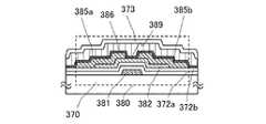
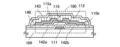
図1(A)乃至(E)に半導体装置の断面構造の一例を示す。図1(A)乃至(E)に示
す薄膜トランジスタ110は、ボトムゲート構造の一つであり逆スタガ型薄膜トランジス
タともいう。1A to 1E illustrate an example of a cross-sectional structure of a semiconductor device. The
図1(A)乃至(E)に示す薄膜トランジスタ110は、絶縁表面を有する基板100上
に、ゲート電極層111、ゲート絶縁層102、酸化物半導体層112、酸素過剰の混合
領域119、ソース電極層115a、及びドレイン電極層115bを含む。また、薄膜ト
ランジスタ110を覆い、酸化物半導体層112に酸素過剰の混合領域119を介して積
層する欠陥を含む絶縁層116が設けられ、さらにその上に保護絶縁層103が積層され
ている。In the
酸素過剰の混合領域119、欠陥を含む絶縁層116は、水素や水分(水素原子や、H2
Oなど水素原子を含む化合物)に対して束縛エネルギーが大きく、酸素過剰の混合領域1
19、欠陥を含む絶縁層116において該不純物は安定化するため、酸化物半導体層11
2から、酸素過剰の混合領域119、欠陥を含む絶縁層116へ該不純物を拡散させ、該
不純物を酸化物半導体層112から排除することができる。さらに、酸素過剰の混合領域
119が欠陥を含む絶縁層116に拡散した不純物に対するバリア層となり、該不純物が
再度酸化物半導体層112に侵入することを防止するため、酸化物半導体層112中の不
純物濃度を低減させた状態で維持することができる。従って、変動要因となる水素、水分
、水酸基又は水素化物(水素化合物ともいう)などの不純物を低減させた酸化物半導体層
112を用いた薄膜トランジスタ110は安定した電気的特性を有する信頼性の高い薄膜
トランジスタとなる。The oxygen-excess
19. The oxide semiconductor layer 11 is used for stabilizing the impurity in the insulating
2, the impurity can be diffused into the oxygen-excess
図19は、酸化物半導体を用いた逆スタガ型の薄膜トランジスタの縦断面図である。ゲー
ト電極(GE1)上にゲート絶縁膜(GI)を介して酸化物半導体層(OS)が設けられ
、その上にソース電極(S)及びドレイン電極(D)が設けられている。FIG. 19 is a vertical cross-sectional view of an inverted staggered thin film transistor using an oxide semiconductor. An oxide semiconductor layer (OS) is provided over the gate electrode (GE1) with a gate insulating film (GI) interposed therebetween, and a source electrode (S) and a drain electrode (D) are provided thereover.
図20は、図19に示されているA−A’断面におけるエネルギーバンド図(模式図)で
ある。図20(A)はソースとドレインの間の電圧を等電位(VD=0V)とした場合を
示し、図20(B)はソースに対しドレインに正の電位(VD>0)を加えた場合を示す
。FIG. 20 is an energy band diagram (schematic diagram) along the AA 'section shown in FIG. FIG. 20A shows a case where the voltage between the source and the drain is equal potential (VD = 0 V), and FIG. 20B shows a case where a positive potential (VD> 0) is applied to the drain with respect to the source. Is shown.
図21は、図19に示されているB−B’断面におけるエネルギーバンド図(模式図)で
ある。図21(A)はゲート(G1)に正の電位(+VG)が印加された状態であり、ソ
ース、ドレイン間にキャリア(電子)が流れるオン状態を示している。また、図21(B
)は、ゲート(G1)に負の電位(−VG)が印加された状態であり、オフ状態(少数キ
ャリアは流れない)である場合を示す。FIG. 21 is an energy band diagram (schematic diagram) in the BB 'section shown in FIG. FIG. 21A shows a state in which a positive potential (+ VG) is applied to the gate (G1), and shows an on state in which carriers (electrons) flow between the source and the drain. FIG. 21 (B
) Shows a state in which a negative potential (−VG) is applied to the gate (G1) and is in an off state (minority carriers do not flow).
図22は、真空準位と金属の仕事関数(φM)、酸化物半導体の電子親和力(χ)の関係
が示されている。FIG. 22 shows the relationship between the vacuum level, the work function of a metal (φM), and the electron affinity (χ) of an oxide semiconductor.
常温において金属中の電子は縮退しているため、フェルミ準位は伝導帯内に位置する。一
方、従来の酸化物半導体は一般にn型であり、その場合のフェルミ準位(Ef)は、バン
ドギャップ中央に位置する真性フェルミ準位(Ei)から離れて、伝導帯寄りに位置して
いる。なお、従来の酸化物半導体が一般にn型となるのは、含有した水素の一部が電子を
供給するドナーとなることが一つの要因であることが知られている。At room temperature, electrons in a metal are degenerate, so that the Fermi level is located in the conduction band. On the other hand, a conventional oxide semiconductor is generally n-type, and in that case, the Fermi level (Ef) is located closer to the conduction band, away from the intrinsic Fermi level (Ei) located at the center of the band gap. . It is known that one reason that a conventional oxide semiconductor generally becomes n-type is that part of hydrogen contained therein becomes a donor for supplying electrons.
これに対して本発明に係る酸化物半導体は、n型不純物である水素を酸化物半導体から除
去し、酸化物半導体の主成分以外の不純物が極力含まれないように高純度化することによ
り真性(i型)とし、又は真性型とせんとしたものである。すなわち、不純物を添加して
i型化するのでなく、水素や水等の不純物を極力除去したことにより、高純度化されたi
型(真性半導体)又はそれに近づけることを特徴としている。そうすることにより、フェ
ルミ準位(Ef)は真性フェルミ準位(Ei)と同じレベルにまでする、或いはそれに限
りなく近づけることができる。In contrast, the oxide semiconductor according to the present invention has an intrinsic property by removing hydrogen as an n-type impurity from the oxide semiconductor and purifying the oxide semiconductor so that impurities other than the main components of the oxide semiconductor are contained as little as possible. (I type) or an intrinsic type. That is, instead of adding impurities to form an i-type, impurities such as hydrogen and water are removed as much as possible, so that highly purified i-type is obtained.
It is characterized in that it is of a type (intrinsic semiconductor) or close to it. By doing so, the Fermi level (Ef) can be brought to the same level as the intrinsic Fermi level (Ei), or can be approached without limit.
酸化物半導体のバンドギャップ(Eg)が3.15eVである場合、電子親和力(χ)は
4.3eVと言われている。ソース電極及びドレイン電極を構成するチタン(Ti)仕事
関数は、上記酸化物半導体の電子親和力(χ)とほぼ等しい。この場合、金属−酸化物半
導体界面において、電子に対してショットキー型の障壁は形成されない。When the band gap (Eg) of the oxide semiconductor is 3.15 eV, the electron affinity (χ) is said to be 4.3 eV. The work function of titanium (Ti) forming the source electrode and the drain electrode is substantially equal to the electron affinity (χ) of the oxide semiconductor. In this case, a Schottky barrier for electrons is not formed at the metal-oxide semiconductor interface.
すなわち、金属の仕事関数(φM)と酸化物半導体の電子親和力(χ)が等しい場合、両
者が接触すると図20(A)で示すようなエネルギーバンド図(模式図)が示される。That is, when the work function (φM) of a metal and the electron affinity (χ) of an oxide semiconductor are the same, an energy band diagram (schematic diagram) as shown in FIG.
図20(B)において黒丸(●)は電子を示し、ドレインに正の電位が印加されると、電
子はバリア(h)をこえて酸化物半導体に注入され、ドレインに向かって流れる。この場
合、バリア(h)の高さは、ゲート電圧とドレイン電圧に依存して変化するが、正のドレ
イン電圧が印加された場合には、電圧印加のない図20(A)のバリアの高さすなわちバ
ンドギャップ(Eg)の1/2よりもバリアの高さ(h)は小さい値となる。In FIG. 20B, black circles (•) indicate electrons, and when a positive potential is applied to the drain, the electrons are injected into the oxide semiconductor over the barrier (h) and flow toward the drain. In this case, the height of the barrier (h) changes depending on the gate voltage and the drain voltage. However, when a positive drain voltage is applied, the height of the barrier shown in FIG. That is, the height (h) of the barrier is smaller than 1 / of the band gap (Eg).
このとき電子は、図21(A)で示すようにゲート絶縁膜と高純度化された酸化物半導体
との界面における、酸化物半導体側のエネルギー的に安定な最低部を移動する。At this time, as shown in FIG. 21A, the electrons move at the lowest energy-stable portion on the oxide semiconductor side at the interface between the gate insulating film and the highly purified oxide semiconductor.
また、図21(B)において、ゲート電極(G1)に負の電位(逆バイアス)が印加され
ると、少数キャリアであるホールは実質的にゼロであるため、電流は限りなくゼロに近い
値となる。In addition, in FIG. 21B, when a negative potential (reverse bias) is applied to the gate electrode (G1), the number of holes, which are minority carriers, is substantially zero. Becomes
例えば、薄膜トランジスタのチャネル幅Wが1×104μmであり、チャネル長が3μm
の素子であっても、オフ電流が10−13A以下、0.1V/dec.(ゲート絶縁膜厚
100nm)のサブスレッショルドスイング値(S値)が得られる。For example, the channel width W of the thin film transistor is 1 × 104 μm, and the channel length is 3 μm.
, The off-state current is 10−13 A or less and 0.1 V / dec. A sub-threshold swing value (S value) of (gate insulating
このように、酸化物半導体の主成分以外の不純物が極力含まれないように高純度化するこ
とにより、薄膜トランジスタの動作を良好なものとすることができる。As described above, the operation of the thin film transistor can be improved by being highly purified so that impurities other than the main components of the oxide semiconductor are not contained as much as possible.
また、薄膜トランジスタ110はシングルゲート構造の薄膜トランジスタを用いて説明し
たが、必要に応じて、チャネル形成領域を複数有するマルチゲート構造の薄膜トランジス
タも形成することができる。Although the
以下、図1(A)乃至(E)を用い、基板100上に薄膜トランジスタ110を作製する
工程を説明する。Hereinafter, a process for manufacturing the
まず、絶縁表面を有する基板100上に導電膜を形成した後、第1のフォトリソグラフィ
工程によりゲート電極層111を形成する。形成されたゲート電極層の端部はテーパ形状
であると、上に積層するゲート絶縁層の被覆性が向上するため好ましい。なお、レジスト
マスクをインクジェット法で形成してもよい。レジストマスクをインクジェット法で形成
するとフォトマスクを使用しないため、製造コストを低減できる。First, after a conductive film is formed over the
絶縁表面を有する基板100に使用することができる基板に大きな制限はないが、少なく
とも、後の加熱処理に耐えうる程度の耐熱性を有していることが必要となる。バリウムホ
ウケイ酸ガラスやアルミノホウケイ酸ガラスなどのガラス基板を用いることができる。Although there is no particular limitation on a substrate that can be used as the
また、ガラス基板としては、後の加熱処理の温度が高い場合には、歪み点が730℃以上
のものを用いると良い。また、ガラス基板には、例えば、アルミノシリケートガラス、ア
ルミノホウケイ酸ガラス、バリウムホウケイ酸ガラスなどのガラス材料が用いられている
。酸化ホウ素と比較して酸化バリウム(BaO)を多く含ませることで、より実用的な耐
熱ガラスが得られる。このため、B2O3よりBaOを多く含むガラス基板を用いること
が好ましい。In the case where the temperature of heat treatment performed later is high, a glass substrate whose strain point is higher than or equal to 730 ° C is preferably used. For the glass substrate, for example, a glass material such as aluminosilicate glass, aluminoborosilicate glass, or barium borosilicate glass is used. By containing more barium oxide (BaO) than boron oxide, a more practical heat-resistant glass can be obtained. Therefore, it is preferable to use a glass substrate containing more BaO than B2 O3 .
なお、上記のガラス基板に代えて、セラミック基板、石英基板、サファイア基板などの絶
縁体でなる基板を用いても良い。他にも、結晶化ガラスなどを用いることができる。また
、プラスチック基板等も適宜用いることができる。Note that a substrate formed of an insulator such as a ceramic substrate, a quartz substrate, or a sapphire substrate may be used instead of the above glass substrate. Alternatively, crystallized glass or the like can be used. Further, a plastic substrate or the like can be used as appropriate.
下地膜となる絶縁膜を基板100とゲート電極層111との間に設けてもよい。下地膜は
、基板100からの不純物元素の拡散を防止する機能があり、窒化シリコン膜、酸化シリ
コン膜、窒化酸化シリコン膜、又は酸化窒化シリコン膜から選ばれた一又は複数の膜によ
る積層構造により形成することができる。An insulating film serving as a base film may be provided between the
また、ゲート電極層111の材料は、モリブデン、チタン、クロム、タンタル、タングス
テン、アルミニウム、銅、ネオジム、スカンジウム等の金属材料又はこれらを主成分とす
る合金材料を用いて、単層で又は積層して形成することができる。The material of the
例えば、ゲート電極層111の2層の積層構造としては、アルミニウム層上にモリブデン
層が積層された2層の積層構造、銅層上にモリブデン層が積層された2層の積層構造、銅
層上に窒化チタン層若しくは窒化タンタル層が積層された2層の積層構造、または窒化チ
タン層上にモリブデン層が積層された2層の積層構造とすることが好ましい。3層の積層
構造としては、タングステン層または窒化タングステン層と、アルミニウムとシリコンの
合金またはアルミニウムとチタンの合金層と、窒化チタン層またはチタン層とを積層した
積層とすることが好ましい。なお、透光性を有する導電膜を用いてゲート電極層を形成す
ることもできる。透光性を有する導電膜としては、透光性導電性酸化物等をその例に挙げ
ることができる。For example, as a two-layer structure of the
次いで、ゲート電極層111上にゲート絶縁層102を形成する。Next, the
ゲート絶縁層102は、プラズマCVD法又はスパッタリング法等を用いて、酸化シリコ
ン層、窒化シリコン層、酸化窒化シリコン層、窒化酸化シリコン層、酸化アルミニウム層
、窒化アルミニウム層、酸化窒化アルミニウム層、窒化酸化アルミニウム層、又は酸化ハ
フニウム層を単層で又は積層で形成することができる。なお、ゲート絶縁層102中に水
素が多量に含まれないようにするためには、スパッタリング法でゲート絶縁層102を成
膜することが好ましい。スパッタリング法により酸化シリコン膜を成膜する場合には、タ
ーゲットとしてシリコンターゲット又は石英ターゲットを用い、スパッタガスとして酸素
又は、酸素及びアルゴンの混合ガスを用いて行う。The
ゲート絶縁層102は、ゲート電極層111側から窒化シリコン層と酸化シリコン層を積
層した構造とすることもできる。例えば、第1のゲート絶縁層としてスパッタリング法に
より膜厚50nm以上200nm以下の窒化シリコン層(SiNy(y>0))を形成し
、第1のゲート絶縁層上に第2のゲート絶縁層として膜厚5nm以上300nm以下の酸
化シリコン層(SiOx(x>0))を積層して、膜厚100nmのゲート絶縁層とする
。ゲート絶縁層の膜厚は、薄膜トランジスタに要求される特性によって適宜設定すればよ
く350nm乃至400nm程度でもよい。The
また、ゲート絶縁層102、酸化物半導体膜120に水素、水酸基及び水分がなるべく含
まれないようにするために、成膜の前処理として、スパッタリング装置の予備加熱室でゲ
ート電極層111が形成された基板100、又はゲート絶縁層102までが形成された基
板100を予備加熱し、基板100に吸着した水素、水分などの不純物を脱離し排気する
ことが好ましい。なお、予備加熱の温度としては、100℃以上400℃以下好ましくは
150℃以上300℃以下である。なお、予備加熱室に設ける排気手段はクライオポンプ
が好ましい。なお、この予備加熱の処理は省略することもできる。またこの予備加熱は、
欠陥を含む絶縁層116の成膜前に、ソース電極層115a、ドレイン電極層115bま
で形成した基板100にも同様に行ってもよい。Further, in order to prevent the
Before formation of the insulating
次いで、ゲート絶縁層102上に、膜厚2nm以上200nm以下の酸化物半導体膜12
0を形成する(図1(A)参照)。Next, an
0 is formed (see FIG. 1A).
なお、酸化物半導体膜120をスパッタリング法により成膜する前に、アルゴンガスを導
入してプラズマを発生させる逆スパッタを行い、ゲート絶縁層102の表面に付着してい
るゴミを除去することが好ましい。逆スパッタとは、ターゲット側に電圧を印加せずに、
アルゴン雰囲気下で基板側にRF電源を用いて電圧を印加して基板近傍にプラズマを形成
して表面を改質する方法である。なお、アルゴン雰囲気に代えて窒素、ヘリウム、酸素な
どを用いてもよい。Note that before the
This is a method in which a voltage is applied to the substrate side using an RF power source in an argon atmosphere to form plasma near the substrate, thereby modifying the surface. Note that nitrogen, helium, oxygen, or the like may be used instead of the argon atmosphere.
酸化物半導体膜120はスパッタリング法により成膜する。酸化物半導体膜120は、I
n−Ga−Zn−O系膜、In−Sn−Zn−O系、In−Al−Zn−O系、Sn−G
a−Zn−O系、Al−Ga−Zn−O系、Sn−Al−Zn−O系、In−Zn−O系
、Sn−Zn−O系、Al−Zn−O系、In−O系、Sn−O系、Zn−O系の酸化物
半導体膜を用いる。本実施の形態では、酸化物半導体膜120をIn−Ga−Zn−O系
金属酸化物ターゲットを用いてスパッタリング法により成膜する。また、酸化物半導体膜
120は、希ガス(代表的にはアルゴン)雰囲気下、酸素雰囲気下、又は希ガス(代表的
にはアルゴン)及び酸素雰囲気下においてスパッタリング法により形成することができる
。また、スパッタリング法を用いる場合、SiO2を2重量%以上10重量%以下含むタ
ーゲットを用いて成膜を行ってもよい。The
n-Ga-Zn-O-based film, In-Sn-Zn-O-based, In-Al-Zn-O-based, Sn-G
a-Zn-O system, Al-Ga-Zn-O system, Sn-Al-Zn-O system, In-Zn-O system, Sn-Zn-O system, Al-Zn-O system, In-O system , Sn—O-based, and Zn—O-based oxide semiconductor films are used. In this embodiment, the
酸化物半導体膜120を成膜する際に用いるスパッタガスは水素、水、水酸基又は水素化
物などの不純物が、濃度ppm程度、濃度ppb程度まで除去された高純度ガスを用いる
ことが好ましい。As a sputtering gas used for forming the
酸化物半導体膜120をスパッタリング法で作製するためのターゲットとして、酸化亜鉛
を主成分とする金属酸化物のターゲットを用いることができる。また、金属酸化物のター
ゲットの他の例としては、In、Ga、及びZnを含む金属酸化物ターゲット(組成比と
して、In2O3:Ga2O3:ZnO=1:1:1[mol数比])を用いることがで
きる。また、In、Ga、及びZnを含む金属酸化物ターゲットとして、In2O3:G
a2O3:ZnO=1:1:2[mol数比]、又はIn2O3:Ga2O3:ZnO=
1:1:4[mol数比]の組成比を有するターゲットを用いることもできる。金属酸化
物ターゲットの充填率は90%以上100%以下、好ましくは95%以上99.9%以下
である。充填率の高い金属酸化物ターゲットを用いることにより、成膜した酸化物半導体
膜は緻密な膜となる。As a target for forming the
a2 O3 : ZnO = 1: 1: 2 [molar ratio] or In2 O3 : Ga2 O3 : ZnO =
A target having a composition ratio of 1: 1: 4 [molar ratio] can also be used. The filling rate of the metal oxide target is from 90% to 100%, preferably from 95% to 99.9%. With the use of a metal oxide target with a high filling rate, a dense oxide semiconductor film is formed.
減圧状態に設定された処理室内に基板を保持し、基板を400℃未満の温度に加熱する。
そして、処理室内の残留水分を除去しつつ水素及び水分が除去されたスパッタガスを導入
し、金属酸化物をターゲットとして基板100上に酸化物半導体膜120を成膜する。処
理室内の残留水分を除去するためには、吸着型の真空ポンプを用いることが好ましい。例
えば、クライオポンプ、イオンポンプ、チタンサブリメーションポンプを用いることが好
ましい。また、排気手段としては、ターボポンプにコールドトラップを加えたものであっ
てもよい。クライオポンプを用いて排気した成膜室は、例えば、水素原子や、H2Oなど
水素原子を含む化合物や、炭素原子を含む化合物等が排気されるため、当該成膜室で成膜
した酸化物半導体膜120に含まれる不純物の濃度を低減できる。The substrate is held in a processing chamber set in a reduced pressure state, and the substrate is heated to a temperature lower than 400 ° C.
Then, a sputtering gas from which hydrogen and moisture have been removed is introduced while moisture remaining in the treatment chamber is removed, and the
酸化物半導体膜120を成膜する場合、酸化物半導体膜120を成膜する処理室はもちろ
んのこと、酸化物半導体膜120に接する膜及び酸化物半導体膜120の成膜前後の工程
において、処理室内に残留する水分が不純物として混入しないよう、クライオポンプなど
の排気手段を用いることが好ましい。In the case where the
成膜条件の一例としては、基板とターゲットの間との距離を100mm、圧力0.6Pa
、直流(DC)電源0.5kW、酸素(酸素流量比率100%)雰囲気下の条件が適用さ
れる。なお、パルス直流(DC)電源を用いると、成膜時に発生する粉状物質(パーティ
クル、ゴミともいう)が軽減でき、膜厚分布も均一となるため好ましい。酸化物半導体膜
120は好ましくは5nm以上30nm以下とする。なお、適用する酸化物半導体材料に
より適切な厚みは異なり、材料に応じて厚みを選択すればよい。As an example of the film forming conditions, the distance between the substrate and the target is 100 mm, and the pressure is 0.6 Pa.
The conditions under an atmosphere of a direct current (DC) power supply of 0.5 kW and oxygen (oxygen
上記のようにして酸化物半導体膜120をスパッタリング法で成膜することで、水素濃度
が低い酸化物半導体膜120を得ることができる。また本明細書において示される水素濃
度は二次イオン質量分析(SIMS:Secondary Ion Mass Spec
trometry)により測定できる定量結果である。By forming the
4 is a quantification result that can be measured by the measurement (trometry).
スパッタリング法にはスパッタ用電源に高周波電源を用いるRFスパッタリング法、直流
電源を用いるDCスパッタリング法、さらにパルス的にバイアスを与えるパルスDCスパ
ッタリング法がある。RFスパッタリング法は主に絶縁膜を成膜する場合に用いられ、D
Cスパッタリング法は主に金属膜を成膜する場合に用いられる。As the sputtering method, there are an RF sputtering method using a high-frequency power supply as a power supply for sputtering, a DC sputtering method using a DC power supply, and a pulse DC sputtering method that applies a bias in a pulsed manner. The RF sputtering method is mainly used for forming an insulating film.
The C sputtering method is mainly used for forming a metal film.
また、材料の異なるターゲットを複数設置できる多元スパッタ装置もある。多元スパッタ
装置は、同一チャンバーで異なる材料膜を積層成膜することも、同一チャンバーで複数種
類の材料を同時に放電させて成膜することもできる。There is also a multi-source sputtering apparatus in which a plurality of targets of different materials can be set. The multi-source sputtering apparatus can form a film by laminating different material films in the same chamber, or form a film by simultaneously discharging a plurality of types of materials in the same chamber.
また、チャンバー内部に磁石機構を備えたマグネトロンスパッタリング法を用いるスパッ
タ装置や、グロー放電を使わずマイクロ波を用いて発生させたプラズマを用いるECRス
パッタリング法を用いるスパッタ装置がある。Further, there are a sputtering apparatus using a magnetron sputtering method having a magnet mechanism inside a chamber, and a sputtering apparatus using an ECR sputtering method using plasma generated by using a microwave without using a glow discharge.
また、スパッタリング法を用いる成膜方法として、成膜中にターゲット物質とスパッタガ
ス成分とを化学反応させて、それらの化合物薄膜を形成するリアクティブスパッタリング
法や、成膜中に基板にも電圧をかけるバイアススパッタリング法もある。In addition, as a film formation method using a sputtering method, a reactive sputtering method in which a target material and a sputter gas component are chemically reacted during film formation to form a thin film of such a compound, or a voltage is applied to a substrate during film formation. There is also a bias sputtering method to be applied.
次いで、酸化物半導体膜120を第2のフォトリソグラフィ工程により島状の酸化物半導
体層121に加工する(図1(B)参照)。また、島状の酸化物半導体層121を形成す
るためのレジストマスクをインクジェット法で形成してもよい。レジストマスクをインク
ジェット法で形成するとフォトマスクを使用しないため、製造コストを低減させることが
できる。Next, the
また、ゲート絶縁層102にコンタクトホールを形成する場合、その工程は酸化物半導体
層121の形成時に行うことができる。In the case where a contact hole is formed in the
なお、ここでの酸化物半導体膜120のエッチングは、ドライエッチングでもウェットエ
ッチングでもよく、両方を用いてもよい。Note that the etching of the
ドライエッチングに用いるエッチングガスとしては、塩素を含むガス(塩素系ガス、例え
ば塩素(Cl2)、塩化硼素(BCl3)、塩化珪素(SiCl4)、四塩化炭素(CC
l4)など)が好ましい。As an etching gas used for the dry etching, a gas containing chlorine (a chlorine-based gas such as chlorine (Cl2 ), boron chloride (BCl3 ), silicon chloride (SiCl4 ), carbon tetrachloride (CC)
l4 ), etc.) are preferred.
また、フッ素を含むガス(フッ素系ガス、例えば四弗化炭素(CF4)、弗化硫黄(SF
6)、弗化窒素(NF3)、トリフルオロメタン(CHF3)など)、臭化水素(HBr
)、酸素(O2)、これらのガスにヘリウム(He)やアルゴン(Ar)などの希ガスを
添加したガスなどを用いることができる。In addition, a gas containing fluorine (a fluorine-based gas such as carbon tetrafluoride (CF4 ), sulfur fluoride (SF)
6 ), nitrogen fluoride (NF3 ), trifluoromethane (CHF3 ) and the like, hydrogen bromide (HBr)
), Oxygen (O2 ), or a gas in which a rare gas such as helium (He) or argon (Ar) is added to these gases.
ドライエッチング法としては、平行平板型RIE(Reactive Ion Etch
ing)法や、ICP(Inductively Coupled Plasma:誘導
結合型プラズマ)エッチング法を用いることができる。所望の加工形状にエッチングでき
るように、エッチング条件(コイル型の電極に印加される電力量、基板側の電極に印加さ
れる電力量、基板側の電極温度等)を適宜調節する。As a dry etching method, a parallel plate type RIE (Reactive Ion Etch) is used.
ing) method or an ICP (Inductively Coupled Plasma) etching method can be used. The etching conditions (the amount of power applied to the coil-type electrode, the amount of power applied to the electrode on the substrate side, the temperature of the electrode on the substrate side, and the like) are appropriately adjusted so that etching can be performed to a desired processed shape.
ウェットエッチングに用いるエッチング液としては、燐酸と酢酸と硝酸を混ぜた溶液、ア
ンモニア過水(31重量%過酸化水素水:28重量%アンモニア水:水=5:2:2)な
どを用いることができる。また、ITO07N(関東化学社製)を用いてもよい。As an etchant used for wet etching, a solution in which phosphoric acid, acetic acid, and nitric acid are mixed, ammonia peroxide (31% by weight hydrogen peroxide: 28% by weight ammonia water: water = 5: 2: 2), or the like may be used. it can. Further, ITO07N (manufactured by Kanto Chemical Co., Ltd.) may be used.
また、ウェットエッチング後のエッチング液はエッチングされた材料と共に洗浄によって
除去される。その除去された材料を含むエッチング液の廃液を精製し、含まれる材料を再
利用してもよい。当該エッチング後の廃液から酸化物半導体層に含まれるインジウム等の
材料を回収して再利用することにより、資源を有効活用し、製造コストを低減させること
ができる。Further, the etchant after the wet etching is removed together with the etched material by washing. A waste liquid of the etching solution containing the removed material may be purified, and the contained material may be reused. By collecting and reusing a material such as indium contained in the oxide semiconductor layer from the waste liquid after the etching, resources can be effectively used and manufacturing cost can be reduced.
所望の加工形状にエッチングできるように、材料に合わせてエッチング条件(エッチング
液、エッチング時間、温度等)を適宜調節する。The etching conditions (such as an etchant, etching time, and temperature) are appropriately adjusted depending on the material so that the material can be etched into a desired shape.
なお、次工程の導電膜を形成する前に逆スパッタを行い、酸化物半導体層121及びゲー
ト絶縁層102の表面に付着しているレジスト残渣などを除去することが好ましい。Note that it is preferable that reverse sputtering be performed before formation of the conductive film in the next step to remove a resist residue or the like attached to the surfaces of the
次いで、ゲート絶縁層102、及び酸化物半導体層121上に、導電膜を形成する。導電
膜はスパッタリング法や真空蒸着法で形成すればよい。導電膜の材料としては、アルミニ
ウム(Al)、クロム(Cr)、銅(Cu)、タンタル(Ta)、チタン(Ti)、モリ
ブデン(Mo)、タングステン(W)からから選ばれた元素、または上述した元素を成分
とする合金か、上述した元素を組み合わせた合金等が挙げられる。また、マンガン(Mn
)、マグネシウム(Mg)、ジルコニウム(Zr)、ベリリウム(Be)、トリウム(T
h)のいずれか一または複数から選択された材料を用いてもよい。また、金属導電膜は、
単層構造でも、2層以上の積層構造としてもよい。例えば、シリコンを含むアルミニウム
膜の単層構造、アルミニウム膜上にチタン膜を積層する2層構造、Ti膜と、そのTi膜
上に重ねてアルミニウム膜を積層し、さらにその上にTi膜を成膜する3層構造などが挙
げられる。また、アルミニウム(Al)に、チタン(Ti)、タンタル(Ta)、タング
ステン(W)、モリブデン(Mo)、クロム(Cr)、ネオジム(Nd)、スカンジウム
(Sc)から選ばれた元素を単数、又は複数組み合わせた膜、合金膜、もしくは窒化膜を
用いてもよい。Next, a conductive film is formed over the
), Magnesium (Mg), zirconium (Zr), beryllium (Be), thorium (T
h) may be used. Also, the metal conductive film is
It may have a single-layer structure or a stacked structure of two or more layers. For example, a single-layer structure of an aluminum film containing silicon, a two-layer structure in which a titanium film is stacked on an aluminum film, a Ti film, an aluminum film stacked on the Ti film, and a Ti film formed thereon For example, a three-layer structure for forming a film may be used. In addition, a single element selected from titanium (Ti), tantalum (Ta), tungsten (W), molybdenum (Mo), chromium (Cr), neodymium (Nd), and scandium (Sc) is added to aluminum (Al). Alternatively, a film, an alloy film, or a nitride film formed by combining a plurality of films may be used.
第3のフォトリソグラフィ工程により導電膜上にレジストマスクを形成し、選択的にエッ
チングを行ってソース電極層115a、ドレイン電極層115bを形成した後、レジスト
マスクを除去する(図1(C)参照)。A resist mask is formed over the conductive film by a third photolithography step, the
第3のフォトリソグラフィ工程でのレジストマスク形成時の露光には、紫外線やKrFレ
ーザ光やArFレーザ光を用いる。酸化物半導体層121上で隣り合うソース電極層の下
端部とドレイン電極層の下端部との間隔幅によって後に形成される薄膜トランジスタのチ
ャネル長Lが決定される。なお、チャネル長L=25nm未満の露光を行う場合には、数
nm〜数10nmと極めて波長が短い超紫外線(Extreme Ultraviole
t)を用いて第3のフォトリソグラフィ工程でのレジストマスク形成時の露光を行う。超
紫外線による露光は、解像度が高く焦点深度も大きい。従って、後に形成される薄膜トラ
ンジスタのチャネル長Lを10nm以上1000nm以下とすることも可能であり、回路
の動作速度を高速化させることができ、さらにオフ電流値が極めて小さいため、低消費電
力化も図ることができる。Ultraviolet light, KrF laser light, or ArF laser light is used for light exposure for forming the resist mask in the third photolithography step. The channel length L of a thin film transistor formed later is determined by the distance between the lower end of the source electrode layer and the lower end of the drain electrode layer which are adjacent to each other over the
Exposure at the time of forming a resist mask in the third photolithography step is performed using t). Exposure with extreme ultraviolet light has a high resolution and a large depth of focus. Therefore, the channel length L of a thin film transistor formed later can be 10 nm or more and 1000 nm or less, the operation speed of the circuit can be increased, and the off-state current value is extremely small; Can be planned.
なお、導電膜のエッチングの際に、酸化物半導体層121は除去されないようにそれぞれ
の材料及びエッチング条件を適宜調節する。Note that each material and etching conditions are appropriately adjusted so that the
本実施の形態では、導電膜としてTi膜を用いて、酸化物半導体層121にはIn−Ga
−Zn−O系酸化物を用いて、エッチャントとしてアンモニア過水(アンモニア、水、過
酸化水素水の混合液)を用いる。In this embodiment, a Ti film is used as the conductive film, and In-Ga is used for the
Using ammonia-hydrogen peroxide (a mixed solution of ammonia, water, and hydrogen peroxide) as an etchant using a Zn-O-based oxide.
なお、第3のフォトリソグラフィ工程では、酸化物半導体層121は一部のみがエッチン
グされ、溝部(凹部)を有する酸化物半導体層となることもある。また、ソース電極層1
15a、ドレイン電極層115bを形成するためのレジストマスクをインクジェット法で
形成してもよい。レジストマスクをインクジェット法で形成するとフォトマスクを使用し
ないため、製造コストを低減させることができる。Note that in the third photolithography step, only part of the
The resist mask for forming the
また、フォトリソグラフィ工程で用いるフォトマスク数及び工程数を削減するため、透過
した光が複数の強度となる露光マスクである多階調マスクによって形成されたレジストマ
スクを用いて、エッチング工程を行ってもよい。多階調マスクを用いて形成したレジスト
マスクは複数の膜厚を有する形状となり、エッチングを行うことでさらに形状を変形させ
ることができるため、異なるパターンに加工する複数のエッチング工程に用いることがで
きる。よって、一枚の多階調マスクによって、少なくとも二種類以上の異なるパターンに
対応するレジストマスクを形成することができる。よって露光マスク数を削減することが
でき、対応するフォトリソグラフィ工程も削減できるため、工程の簡略化が可能となる。In order to reduce the number of photomasks and the number of steps used in the photolithography step, an etching step is performed using a resist mask formed using a multi-tone mask which is an exposure mask in which transmitted light has a plurality of intensities. Is also good. A resist mask formed using a multi-tone mask has a shape with a plurality of thicknesses and can be further deformed by etching; therefore, the resist mask can be used in a plurality of etching steps for processing into different patterns. . Therefore, a resist mask corresponding to at least two or more types of different patterns can be formed with one multi-tone mask. Therefore, the number of exposure masks can be reduced and the number of corresponding photolithography steps can be reduced, so that the steps can be simplified.
N2O、N2、またはArなどのガスを用いたプラズマ処理によって露出している酸化物
半導体層の表面に付着した吸着水などを除去してもよい。また、酸素とアルゴンの混合ガ
スを用いてプラズマ処理を行ってもよい。Adsorbed water or the like attached to an exposed surface of the oxide semiconductor layer may be removed by plasma treatment using a gas such as N2 O, N2 , or Ar. Alternatively, plasma treatment may be performed using a mixed gas of oxygen and argon.
大気に触れることなく、酸化物半導体層121上に欠陥を含む絶縁層116を形成する。
欠陥を含む絶縁層116の形成工程において、酸化物半導体層121と欠陥を含む絶縁層
116との間に酸素過剰の混合領域119を形成する(図1(D)参照)。本実施の形態
では、酸化物半導体層121がソース電極層115a、ドレイン電極層115bと重なら
ない領域において、酸化物半導体層121と欠陥を含む絶縁層116とが酸素過剰の混合
領域119を介して積層するように形成する。The insulating
In the step of forming the insulating layer having defects, a
混合領域119は、酸化物半導体層121及び積層する欠陥を含む絶縁層116に含まれ
る材料の混合領域119であり、酸化物半導体層121と欠陥を含む絶縁層116の界面
を明確にしないことで、より酸化物半導体層121から欠陥を含む絶縁層116への水素
の拡散が容易になる。例えば、欠陥を含む絶縁層116として酸化シリコン層を用いる場
合、混合領域119には、酸素、シリコン、及び酸化物半導体層121に含まれる金属元
素が少なくとも一種類以上含まれる。The
本実施の形態のように、欠陥を含む絶縁層116として酸化シリコン、酸化物半導体とし
てIn−Ga−Zn−O系膜を用いる場合、混合領域119には、In、Ga、及びZn
のうち少なくとも一種以上の金属元素と、酸素、及びシリコンが含まれる。混合領域11
9において酸化物半導体に含まれる金属をMとすると、M−OH、M−H、M−O−Si
−H、M−O−Si−OHなど様々な状態で存在することができ、例えばZn−HやZn
−OHなどが考えられる。When silicon oxide is used for the insulating
At least one metal element, oxygen, and silicon. Mixed area 11
9, when the metal contained in the oxide semiconductor is M, M-OH, MH, and M-O-Si
-H, MO-Si-OH, etc., and can exist in various states, for example, Zn-H or Zn-H.
—OH and the like are considered.
混合領域119は、膜厚0.1nm乃至30nm(好ましくは2nm乃至10nm)とす
ればよい。混合領域119の膜厚は、欠陥を含む絶縁層116を形成する際のスパッタリ
ング法の成膜条件によって制御することができる。スパッタリング法の電源のパワーをよ
り強くし、基板とターゲット間の距離をより近くすれば、混合領域119を厚く形成する
ことができる。また、より強いパワーでスパッタリング法を行うことによって、酸化物半
導体層121表面に付着した吸着水等を除去することもできる。The
混合領域119を酸化物半導体層121と欠陥を含む絶縁層116との間に設けることに
よって、上記酸化物半導体層121に含まれる水素原子や、H2Oなど水素原子を含む化
合物や、炭素原子を含む化合物等が欠陥を含む絶縁層116へより拡散し易くなる。By providing the
混合領域119は酸素過剰とする必要があるため、混合領域119の形成時には酸素過剰
となるような酸素を多く含むスパッタガスを使用し、混合領域119の形成後はスパッタ
ガス中の酸素量を変化させる調整を行って欠陥を含む絶縁層116を形成してもよい。Since the
よって、欠陥を含む絶縁層116は、酸化シリコン層に代えて、酸化窒化シリコン層、酸
化アルミニウム層、または酸化窒化アルミニウム層などを用いることもできる。また、欠
陥を含む絶縁層116として、窒化シリコン層、窒化酸化シリコン層、窒化アルミニウム
層、窒化酸化アルミニウム層などを用いてもよい。Therefore, instead of the silicon oxide layer, a silicon oxynitride layer, an aluminum oxide layer, an aluminum oxynitride layer, or the like can be used as the insulating
本実施の形態では、島状の酸化物半導体層121、ソース電極層115a、ドレイン電極
層115bまで形成された基板100を室温又は100℃未満の温度に加熱し、水素及び
水分が除去された高純度酸素を含むスパッタガスを導入し、シリコンターゲットを用いて
、酸素過剰の混合領域119、及び酸化シリコン層を成膜する。In this embodiment, the
欠陥を含む絶縁層116を、成膜する際に用いるスパッタガスには水素、水、水酸基又は
水素化物などの不純物が、濃度ppm程度、濃度ppb程度まで除去された高純度ガスを
用いることが好ましい。As a sputtering gas used for forming the insulating
例えば、純度が6Nであり、ボロンがドープされたシリコンターゲット(抵抗値0.01
Ωcm)を用い、基板とターゲット間の距離(T−S間距離)を89mm、圧力0.4P
a、直流(DC)電源6kW、酸素(酸素流量比率100%)雰囲気下でパルスDCスパ
ッタリング法により酸化シリコン膜を成膜する。膜厚は300nmとする。なお、シリコ
ンターゲットに代えて石英(好ましくは合成石英)を酸化シリコン膜の成膜のためのター
ゲットとして用いることができる。なお、スパッタガスとして酸素又は、酸素及びアルゴ
ンの混合ガスを用いて行う。For example, a silicon target having a purity of 6N and doped with boron (resistance value 0.01
Ωcm), the distance between the substrate and the target (distance between TS) is 89 mm, and the pressure is 0.4 P
a, A silicon oxide film is formed by a pulse DC sputtering method in a DC (DC) power supply of 6 kW and in an oxygen (oxygen flow rate ratio: 100%) atmosphere. The thickness is 300 nm. Note that instead of a silicon target, quartz (preferably, synthetic quartz) can be used as a target for forming a silicon oxide film. Note that oxygen or a mixed gas of oxygen and argon is used as a sputtering gas.
また、処理室内の残留水分を除去しつつ混合領域119及び欠陥を含む絶縁層116を成
膜することが好ましい。これは、酸化物半導体層121、混合領域119及び欠陥を含む
絶縁層116に水素、水酸基又は水分が含まれないようにするためである。Further, it is preferable to form the
なお、混合領域119は、酸化シリコンに代えて、酸化窒化シリコン、酸化アルミニウム
、または酸化窒化アルミニウムなどを用いて形成してもよい。Note that the
次に、欠陥を含む絶縁層116と酸化物半導体層121が酸素過剰の混合領域119を介
して接した状態で100℃乃至400℃の加熱処理を行う。この加熱処理によって酸化物
半導体層121中に含まれる水素若しくは水分を酸素過剰の混合領域119、欠陥を含む
絶縁層116に拡散させることができる。欠陥を含む絶縁層116と酸化物半導体層12
1との間に酸素過剰の混合領域119が設けられているため、島状の酸化物半導体層12
1に含まれる水素、水酸基、及び水分等の不純物は、酸化物半導体層121から酸素過剰
の混合領域119へ、または酸素過剰の混合領域119を通過して欠陥を含む絶縁層11
6へと拡散する。Next, heat treatment at 100 ° C to 400 ° C is performed in a state where the insulating
1, the
1, impurities such as hydrogen, hydroxyl groups, and moisture from the
Diffusion to 6.
酸化物半導体層121と欠陥を含む絶縁層116との間に設けられる、混合領域119は
酸素過剰であるため、酸素の未結合手を欠陥として多く含み、水素、水分、水酸基又は水
素化物などの不純物に対して束縛エネルギーが大きい。よって、酸素過剰の混合領域11
9を設けることで、酸化物半導体層121に含まれる水素、水分、水酸基又は水素化物な
どの不純物が欠陥を含む絶縁層116に拡散し移動し易くなる。Since the
With the provision of 9, impurities such as hydrogen, moisture, a hydroxyl group, or hydride contained in the
さらに、上記不純物が一旦酸化物半導体層121から排除され欠陥を含む絶縁層116へ
拡散した後、再度酸化物半導体層121へ移動しようとする際は、酸素過剰の混合領域1
19は、上記不純物を束縛して安定化させ、酸化物半導体層121への上記不純物の侵入
を防止する保護層(バリア層)として機能する。Further, when the impurities are once removed from the
Reference numeral 19 functions as a protective layer (barrier layer) that binds and stabilizes the impurities and prevents the impurities from entering the
このように、変動要因となる水素、水分、水酸基又は水素化物などの不純物を酸化物半導
体層121より排除することで、上記不純物が低減された酸化物半導体層112を得るこ
とができる。さらに、バリア層となる酸素過剰の混合領域119が欠陥を含む絶縁層11
6に拡散した不純物が再度酸化物半導体層112に侵入することを防止することによって
、酸化物半導体層112中の不純物濃度を低減させた状態で維持することができる。In this manner, by removing impurities such as hydrogen, moisture, a hydroxyl group, or a hydride which cause a change from the
By preventing the impurities diffused into 6 from entering the
酸化物半導体層と欠陥を含む絶縁層との間に設けられる酸素過剰の混合領域、又は酸素過
剰の酸化物絶縁層は、酸素過剰であるため、酸素の未結合手を欠陥として多く含む欠陥を
含む。酸化物半導体層からこのような欠陥を含む絶縁層への水素の拡散について、水素原
子が酸化物半導体層(アモルファスIGZO)内と欠陥を含む絶縁層(アモルファスSi
Ox)内のどちらに存在しやすいかを計算した。An oxygen-excess mixed region provided between the oxide semiconductor layer and the insulating layer containing defects, or the oxygen-excess oxide insulating layer has an excess of oxygen, and thus includes defects including many dangling bonds of oxygen as defects. Including. Regarding diffusion of hydrogen from the oxide semiconductor layer to the insulating layer including such a defect, hydrogen atoms are contained in the oxide semiconductor layer (amorphous IGZO) and the insulating layer including the defect (amorphous Si).
Ox ) was calculated where it is more likely to be present.
環境における水素原子の安定性を評価するために水素原子の束縛エネルギーE_bind
を以下で定義し、評価を行った。E_bind={E(元の構造)+E(H)}−E(H
を付加した構造)。この束縛エネルギーE_bindが大きい方が水素原子は存在しやす
いといえる。E(元の構造)、E(H)、E(Hを付加した構造)はそれぞれ、元の構造
のエネルギー、水素原子のエネルギー、Hを付加した構造のエネルギーを表す。この束縛
エネルギーをアモルファスIGZO、ダングリングボンド(以下、DBと略す)無しのア
モルファスSiO2、DB有りのアモルファスSiOxを2種類、の計4つに対して計算
した。To evaluate the stability of hydrogen atoms in the environment, the binding energy E_bind of hydrogen atoms
Was defined below and evaluated. E_bind = {E (original structure) + E (H)} − E (H
Added structure). It can be said that the larger the binding energy E_bind is, the more likely a hydrogen atom is present. E (original structure), E (H) and E (structure with H added) represent the energy of the original structure, the energy of the hydrogen atom, and the energy of the structure with H added, respectively. The binding energies were calculated for amorphous IGZO, amorphous SiO2 without dangling bonds (hereinafter abbreviated as DB), and amorphous SiO x with DB, two types, for a total of four.
計算には密度汎関数法のプログラムであるCASTEPを用いた。密度汎関数の方法とし
て平面波基底擬ポテンシャル法を用い、汎関数はLDAを用いた。カットオフエネルギー
は300eVを用いた。k点は2×2×2のグリッドを用いた。CASTEP, a program of the density functional theory, was used for the calculation. A plane wave basis pseudopotential method was used as a method of the density functional, and LDA was used as the functional. The cutoff energy used was 300 eV. As the k points, a 2 × 2 × 2 grid was used.
計算した構造に関して以下に記す。はじめに元の構造に関して以下に記す。アモルファス
IGZOのユニットセルはInを12原子、Gaを12原子、Znを12原子、Oを48
原子、計84原子を含む。DB無しのアモルファスSiO2のユニットセルはSiを16
原子、Oを32原子、計48原子を含む。DB有りのアモルファスSiOx(1)は、D
Bの無いアモルファスSiO2からOを抜き、上記Oと結合していたSiの内1つにHを
結合させた構造である。つまり、Siを16原子、Oを31原子、Hを1原子、計48原
子を含む。DB有りのアモルファスSiOx(2)は、DBの無いアモルファスSiO2
からSiを抜き、上記Siと結合していたOの内3つにHを結合させた構造である。つま
り、Siを15原子、Oを32原子、Hを3原子、計50原子を含む。Hを付加した構造
は上記の4つの構造にHを付加した構造である。尚、Hは、アモルファスIGZOではO
原子、DBの無いアモルファスSiO2ではSi、DB有りのアモルファスSiOxでは
DBを有する原子に付加した。Hを計算した構造はユニットセル内にHを一つ含む。なお
、各構造のセルサイズを表1にまとめた。The calculated structure is described below. First, the original structure is described below. The unit cell of the amorphous IGZO has 12 atoms of In, 12 atoms of Ga, 12 atoms of Zn, and 48 atoms of O.
Atoms, including a total of 84 atoms. Amorphous SiO2 unit cell without DB has 16 Si
Atom, O 32 atoms, including 48 atoms in total. Amorphous SiOx (1) with DB is D
In this structure, O is extracted from amorphous SiO2 having no B, and H is bonded to one of the Si bonded to O. That is, it includes 16 atoms of Si, 31 atoms of O, and 1 atom of H, for a total of 48 atoms. Amorphous SiOx (2) with DB is amorphous SiO2 without DB
From Si, and H is bonded to three of the Os bonded to the Si. That is, 15 atoms of Si, 32 atoms of O, 3 atoms of H, and a total of 50 atoms are included. The structure to which H is added is a structure in which H is added to the above four structures. Note that H is O in amorphous IGZO.
Atom, Si in the amorphous SiO2 without DB, and added to the atom with DB in amorphous SiOx the presence DB. The structure in which H is calculated includes one H in the unit cell. Table 1 shows the cell size of each structure.

計算結果を表2に示す。Table 2 shows the calculation results.
以上より、Siを抜き該Siと結合していたOの内3つにHを結合させたDBがある場合
のアモルファスSiOx(2)が最も束縛エネルギーが大きく、次にOを抜き該Oと結合
していたSiの内1つにHを結合させたSiOx(1)、次にIGZO、最も小さいのが
DB無しのアモルファスSiO2の順となった。よって、水素は酸素過剰によるDBがあ
る場合のアモルファスSiOx中のDBに結合した場合に最も安定となる。As described above, amorphous SiOx (2) in the case where there is a DB in which H is bonded to three of the Os that have been extracted with Si and bonded to the Si has the largest binding energy, and then the O is extracted and bonded to the O. SiOx (1) in which H was bonded to one of the Sis, followed by IGZO, and the smallest was amorphous SiO2 without DB. Therefore, hydrogen becomes most stable when it is bonded to DB in amorphous SiOx when DB due to oxygen excess exists.
よって、以下のような過程が考えられる。アモルファスSiOxは多量のDBが存在する
。従って、アモルファスIGZO―アモルファスSiOx界面に拡散する水素原子はアモ
ルファスSiOx内のDBに捉えられる事で安定化する。よって、アモルファスIGZO
内の水素原子はアモルファスSiOx中のDBに移動する。Therefore, the following process can be considered. Amorphous SiOx has a large amount of DB. Therefore, hydrogen atoms diffusing at the interface between the amorphous IGZO and the amorphous SiOx are stabilized by being captured by the DB in the amorphous SiOx. Therefore, amorphous IGZO
The hydrogen atoms inside move to DB in amorphous SiOx.
さらに、Siを抜くことでタングリングボンドを発生させた構造であるDBがある場合の
アモルファスSiOx(2)が、Oを抜くことでタングリングボンドを発生させた構造で
あるDBがある場合のアモルファスSiOx(1)より束縛エネルギーが大きいことから
、SiOxにおいて、水素原子はOと結合することでより安定する。Further, amorphous SiOx (2) in the case where there is a DB having a structure in which a tangling bond is generated by removing Si is different from amorphous SiOx (2) in the case where there is a DB in which a tangling bond is generated by removing O. Since the binding energy is larger than that of SiOx (1), hydrogen atoms in SiOx are more stable by bonding to O.
欠陥を含む絶縁層において、酸素の未結合手を欠陥として多く含む絶縁層であると、水素
に対する束縛エネルギーが大きくなるので、より酸化物半導体層から、水素若しくは水素
を含む不純物を、欠陥を含む絶縁層に拡散させることができる。従って、酸化物半導体層
と接する混合領域、又は酸化物絶縁層は、酸素過剰であることが好ましく、SiO2+x
において好ましくはxは0以上3未満であることが望ましい。In the insulating layer containing defects, when the insulating layer contains many dangling bonds of oxygen as defects, binding energy with respect to hydrogen is increased, so that the oxide semiconductor layer contains hydrogen or impurities containing hydrogen, which contain defects. It can be diffused into the insulating layer. Therefore, the mixed region in contact with the oxide semiconductor layer or the oxide insulating layer is preferably oxygen-excessive, and SiO2 + x
Is preferably 0 or more and less than 3.
以上の工程で、水素及び水素化物の濃度が低減された酸化物半導体層112を有する薄膜
トランジスタ110を形成することができる(図1(E)参照)。このように水素や水分
などの不純物を極低濃度とすることによって、酸化物半導体層表層部のバックチャネル側
での寄生チャネルの発生を抑えることができる。Through the above steps, the
薄膜トランジスタ110は、酸化物半導体に含まれる水素が5×10¹⁹/cm3以下、
好ましくは5×10¹⁸/cm3以下、より好ましくは5×1017/cm3以下として
、酸化物半導体に含まれる水素若しくはOH基を除去し、キャリア濃度を5×10¹⁴/
cm3以下、好ましくは5×10¹²/cm3以下とした酸化物半導体層でチャネル形成
領域が形成される薄膜トランジスタとすることができる。In the
Hydrogen or OH groups contained in the oxide semiconductor are removed at preferably 5 × 10¹⁸ / cm3 or less, more preferably 5 × 10¹⁷ / cm3 or less, and the carrier concentration is 5 × 10¹⁴ / cm3.
A thin film transistor in which a channel formation region is formed using an oxide semiconductor layer having a thickness of less than or equal to3 cm3 , preferably less than or equal to 5 x 10¹² / cm3 can be obtained.
酸化物半導体のエネルギーギャップは2eV以上、好ましくは2.5eV以上、より好ま
しくは3eV以上として、ドナーを形成する水素等の不純物を極力低減させ、キャリア濃
度を1×10¹⁴/cm3以下、好ましくは1×1012/cm3以下となるようにする
。The energy gap of the oxide semiconductor is higher than or equal to 2 eV, preferably higher than or equal to 2.5 eV, and more preferably higher than or equal to 3 eV, in which impurities such as hydrogen forming a donor are reduced as much as possible, and the carrier concentration is lower than or equal to 1 × 10¹⁴ / cm3 , preferably. Is set to 1 × 10¹² / cm3 or less.
このように高純度化された酸化物半導体を、薄膜トランジスタ110のチャネル形成領域
に用いることで、チャネル幅が10mmの場合でさえも、ドレイン電圧が1V及び10V
の場合において、ゲート電圧が−5Vから−20Vの範囲において、ドレイン電流は1×
10−13A以下となるように作用する。With the use of such a purified oxide semiconductor for a channel formation region of the
In the case of the above, when the gate voltage is in the range of −5 V to −20 V, the drain current is 1 ×
It acts so as to be 10−13 A or less.
上記のように酸化物半導体膜を成膜するに際し、反応雰囲気中の残留水分を除去すること
で、該酸化物半導体膜中の水素及び水素化物の濃度を低減させることができる。また、酸
化物半導体層上に酸素過剰の混合領域を介して欠陥を含む絶縁層を設けることで酸化物半
導体層中の水素、水分等の不純物を、欠陥を含む絶縁層へ拡散させ酸化物半導体層の水素
及び水素化合物の濃度を低減させることができる。それにより酸化物半導体層の安定化を
図ることができる。By removing residual moisture in the reaction atmosphere when the oxide semiconductor film is formed as described above, the concentration of hydrogen and hydride in the oxide semiconductor film can be reduced. In addition, an insulating layer including a defect is provided over the oxide semiconductor layer through a mixed region containing excess oxygen, whereby impurities such as hydrogen and moisture in the oxide semiconductor layer are diffused into the insulating layer including the defect and the oxide semiconductor The concentration of hydrogen and hydride in the layer can be reduced. Thus, the oxide semiconductor layer can be stabilized.
欠陥を含む絶縁層上に保護絶縁層を設けてもよい。本実施の形態では、保護絶縁層103
を欠陥を含む絶縁層116上に形成する。保護絶縁層103としては、窒化シリコン膜、
窒化酸化シリコン膜、または窒化アルミニウム膜などを用いる。A protective insulating layer may be provided over the insulating layer having defects. In this embodiment mode, the protective insulating
Is formed on the insulating
A silicon nitride oxide film, an aluminum nitride film, or the like is used.
保護絶縁層103として、欠陥を含む絶縁層116まで形成された基板100を100℃
〜400℃の温度に加熱し、水素及び水分が除去された高純度窒素を含むスパッタガスを
導入しシリコンターゲットを用いて窒化シリコン膜を成膜する。この場合においても、欠
陥を含む絶縁層116と同様に、処理室内の残留水分を除去しつつ保護絶縁層103を成
膜することが好ましい。As the protective insulating
Heat to a temperature of about 400 ° C., introduce a sputtering gas containing high-purity nitrogen from which hydrogen and moisture have been removed, and form a silicon nitride film using a silicon target. Also in this case, it is preferable that the protective insulating
保護絶縁層103を形成する場合、保護絶縁層103の成膜時に100℃〜400℃に基
板100を加熱することで、酸化物半導体層中に含まれる水素若しくは水分等の不純物を
、欠陥を含む絶縁層116に拡散させることができる。この場合、上記欠陥を含む絶縁層
116の形成後に加熱処理を行わなくてもよい。In the case where the protective insulating
欠陥を含む絶縁層116として酸化シリコン層を形成し、保護絶縁層103として窒化シ
リコン層を積層する場合、酸化シリコン層と窒化シリコン層を同じ処理室において、共通
のシリコンターゲットを用いて成膜することができる。先に酸素を含むスパッタガスを導
入して、処理室内に装着されたシリコンターゲットを用いて酸化シリコン層を形成し、次
にスパッタガスを窒素を含むスパッタガスに切り替えて同じシリコンターゲットを用いて
窒化シリコン層を成膜する。酸化シリコン層と窒化シリコン層とを大気に曝露せずに連続
して形成することができるため、酸化シリコン層表面に水素や水分などの不純物が吸着す
ることを防止することができる。この場合、欠陥を含む絶縁層116として酸化シリコン
層を形成し、保護絶縁層103として窒化シリコン層を積層した後、酸化物半導体層中に
含まれる水素若しくは水分を欠陥を含む絶縁層に拡散させるための加熱処理(温度100
℃乃至400℃)を行うとよい。In the case where a silicon oxide layer is formed as the insulating
To 400 ° C.).
保護絶縁層の形成後、さらに大気中、100℃以上200℃以下、1時間以上30時間以
下での加熱処理を行ってもよい。この加熱処理は一定の加熱温度を保持して加熱してもよ
いし、室温から、100℃以上200℃以下の加熱温度への昇温と、加熱温度から室温ま
での降温を複数回繰り返して行ってもよい。また、この加熱処理を、保護絶縁層の形成前
に、減圧下で行ってもよい。減圧下で加熱処理を行うと、加熱時間を短縮することができ
る。この加熱処理によって、ノーマリーオフとなる薄膜トランジスタを得ることができる
。よって半導体装置の信頼性を向上させることができる。After the formation of the protective insulating layer, heat treatment may be further performed in the air at 100 ° C. to 200 ° C. for 1 hour to 30 hours. In this heat treatment, heating may be performed while maintaining a constant heating temperature, or a temperature rise from room temperature to a heating temperature of 100 ° C. or more and 200 ° C. or less, and a temperature decrease from the heating temperature to room temperature may be repeated several times. You may. This heat treatment may be performed under reduced pressure before the formation of the protective insulating layer. When the heat treatment is performed under reduced pressure, the heating time can be reduced. Through this heat treatment, a normally-off thin film transistor can be obtained. Therefore, the reliability of the semiconductor device can be improved.
欠陥を含む絶縁層116に不純物を拡散させた後の加熱工程によって、不純物が酸化物半
導体層112へ再度移動したとしても、バリア層となる酸素過剰の混合領域119が上記
不純物の酸化物半導体層112への侵入を防止する。よって、酸化物半導体層112中の
不純物濃度を低減させた状態で維持することができる。Even if the impurity is transferred to the
上記の工程は、液晶表示パネル、エレクトロルミネセンス表示パネル、電子インクを用い
た表示装置などのバックプレーン(薄膜トランジスタが形成された基板)の製造に用いる
ことができる。上記の工程は、400℃以下の温度で行うことが可能なため、厚さが1m
m以下で、一辺が1mを超えるガラス基板を用いる製造工程に好適に適用することができ
る。The above steps can be used for manufacturing a backplane (a substrate on which a thin film transistor is formed) such as a liquid crystal display panel, an electroluminescence display panel, or a display device using electronic ink. Since the above process can be performed at a temperature of 400 ° C. or less, the thickness is 1 m.
m or less, and can be suitably applied to a manufacturing process using a glass substrate whose one side exceeds 1 m.
以上のように、酸化物半導体層を用いる薄膜トランジスタを有する半導体装置において、
安定した電気的特性を有し信頼性の高い半導体装置を提供することができる。As described above, in a semiconductor device including a thin film transistor including an oxide semiconductor layer,
A highly reliable semiconductor device having stable electric characteristics can be provided.
(実施の形態2)
本実施の形態は、本明細書で開示する半導体装置に適用できる薄膜トランジスタの他の例
を示す。上記実施の形態と同一部分又は同様な機能を有する部分、及び工程は、上記実施
の形態を適用することができ、繰り返しの説明は省略する。また同じ箇所の詳細な説明は
省略する。(Embodiment 2)
This embodiment shows another example of a thin film transistor which can be applied to the semiconductor device disclosed in this specification. The above embodiment can be applied to the same portion or a portion having the same function as the above embodiment, and a step, and a repeated description is omitted. A detailed description of the same parts is omitted.
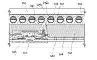
図2(A)乃至(D)に半導体装置の断面構造の一例を示す。図2(A)乃至(D)に示
す薄膜トランジスタ130は、ボトムゲート構造の一つであり逆スタガ型薄膜トランジス
タともいう。2A to 2D illustrate an example of a cross-sectional structure of a semiconductor device. The
図2(A)乃至(D)に示す薄膜トランジスタ130は、絶縁表面を有する基板100上
に、ゲート電極層111、ゲート絶縁層102、酸化物半導体層132、ソース電極層1
15a、及びドレイン電極層115bを含む。また、薄膜トランジスタ130を覆い、酸
化物半導体層132に接して酸素過剰な酸化物絶縁層139が設けられ、酸素過剰な酸化
物絶縁層139上に欠陥を含む絶縁層116が形成されている。さらに欠陥を含む絶縁層
116上に保護絶縁層103が積層されている。A
15a and a
酸素過剰な酸化物絶縁層139、欠陥を含む絶縁層116は、水素や水分(水素原子や、
H2Oなど水素原子を含む化合物)に対して束縛エネルギーが大きく、酸素過剰な酸化物
絶縁層139、欠陥を含む絶縁層116において該不純物は安定化するため、酸化物半導
体層121から、酸素過剰な酸化物絶縁層139、欠陥を含む絶縁層116へ該不純物を
拡散させ、該不純物を酸化物半導体層132から排除することができる。さらに、酸素過
剰な酸化物絶縁層139が欠陥を含む絶縁層116に拡散した不純物に対するバリア層と
なり、該不純物が再度酸化物半導体層132に侵入することを防止するため、酸化物半導
体層132中の不純物濃度は低減された状態で維持されることができる。従って、変動要
因となる水素、水分、水酸基又は水素化物(水素化合物ともいう)などの不純物が低減さ
れた酸化物半導体層132を用いた薄膜トランジスタ130は安定した電気的特性を有す
る信頼性の高い薄膜トランジスタとなる。The oxygen-excess
H2 O, which is a compound containing a hydrogen atom, has high binding energy, and the impurity is stabilized in the oxygen-excess
酸素過剰な酸化物絶縁層139としては、酸化シリコン層(SiO2+x、好ましくはx
は0以上3未満)を用いることができる。酸素過剰な酸化物絶縁層139は、膜厚0.1
nm乃至30nm(好ましくは2nm乃至10nm)とすればよい。As the oxygen-excess
Is 0 or more and less than 3). The oxygen-excess
nm to 30 nm (preferably, 2 nm to 10 nm).
また、薄膜トランジスタ130はシングルゲート構造の薄膜トランジスタを用いて説明し
たが、必要に応じて、チャネル形成領域を複数有するマルチゲート構造の薄膜トランジス
タも形成することができる。Although the
以下、図2(A)乃至(D)を用い、基板100上に薄膜トランジスタ130を作製する
工程を説明する。Hereinafter, a process of manufacturing the
まず、絶縁表面を有する基板100上に導電膜を形成した後、第1のフォトリソグラフィ
工程によりゲート電極層111を形成する。First, after a conductive film is formed over the
次いで、ゲート電極層111上にゲート絶縁層102を形成する。ゲート絶縁層102は
、ゲート電極層111側から窒化シリコン層と酸化シリコン層の積層構造を用いることが
できる。Next, the
次いで、ゲート絶縁層102上に、酸化物半導体膜を形成し、第2のフォトリソグラフィ
工程により島状の酸化物半導体層121に加工する。本実施の形態では、酸化物半導体膜
をしてIn−Ga−Zn−O系金属酸化物ターゲットを用いてスパッタリング法により成
膜する。Next, an oxide semiconductor film is formed over the
次いで、ゲート絶縁層102、及び酸化物半導体層121上に、導電膜を形成する。第3
のフォトリソグラフィ工程により導電膜上にレジストマスクを形成し、選択的にエッチン
グを行ってソース電極層115a、ドレイン電極層115bを形成した後、レジストマス
クを除去する(図2(A)参照)。Next, a conductive film is formed over the
A resist mask is formed over the conductive film by the photolithography step described above, and after selectively etching to form the
次いで、ゲート絶縁層102、酸化物半導体層121、ソース電極層115a、及びドレ
イン電極層115b上に、酸素過剰の酸化物絶縁層139を形成する(図2(B)参照)
。本実施の形態では、酸化物半導体層121がソース電極層115a、ドレイン電極層1
15bと重ならない領域において、酸化物半導体層121と酸素過剰の酸化物絶縁層13
9とが接するように形成する。Next, an oxygen-excess
. In this embodiment, the
In the region not overlapping with 15b, the
9 is formed so as to be in contact therewith.
本実施の形態では、酸素過剰の酸化物絶縁層139として、ソース電極層115a、及び
ドレイン電極層115bまで形成された基板100を室温又は100℃未満の温度に加熱
し、水素及び水分が除去された高純度酸素を含むスパッタガスを導入しシリコンターゲッ
トを用いて、酸化シリコン層(SiO2+x、好ましくはxは0以上3未満)を成膜する
。酸素過剰の酸化物絶縁層139は、膜厚0.1nm乃至30nm(好ましくは2nm乃
至10nm)とすればよい。In this embodiment, the
酸素過剰の酸化物絶縁層139を成膜する際に用いるスパッタガスは水素、水、水酸基又
は水素化物などの不純物が、濃度ppm程度、濃度ppb程度まで除去された高純度ガス
を用いることが好ましい。As a sputtering gas used for forming the oxygen-excess
例えば、純度が6Nであり、ボロンがドープされたシリコンターゲット(抵抗値0.01
Ωcm)を用い、基板とターゲット間の距離(S−T間距離)を89mm、圧力0.4P
a、直流(DC)電源6kW、酸素(酸素流量比率100%)雰囲気下でパルスDCスパ
ッタリング法により酸化シリコン層を成膜する。なお、シリコンターゲットに代えて石英
(好ましくは合成石英)を、酸化シリコン層を成膜するためのターゲットとして用いるこ
ともできる。なお、スパッタガスとして酸素又は、酸素及びアルゴンの混合ガスを用いて
行う。For example, a silicon target having a purity of 6N and doped with boron (resistance value 0.01
Ωcm), the distance between the substrate and the target (distance between ST) is 89 mm, and the pressure is 0.4 P
a, A silicon oxide layer is formed by a pulse DC sputtering method in a DC (DC) power supply of 6 kW and an oxygen (oxygen flow rate ratio of 100%) atmosphere. Note that instead of a silicon target, quartz (preferably, synthetic quartz) can be used as a target for forming a silicon oxide layer. Note that oxygen or a mixed gas of oxygen and argon is used as a sputtering gas.
なお、酸素過剰の酸化物絶縁層139は、酸化シリコン層に代えて、酸化窒化シリコン層
、酸化アルミニウム層、または酸化窒化アルミニウム層などを用いることもできる。Note that for the oxygen-excess
次に、大気に触れることなく、酸素過剰の酸化物絶縁層139上に欠陥を含む絶縁層11
6を形成する。Next, the insulating layer 11 containing a defect is formed on the oxygen-excess
6 is formed.
本実施の形態では、島状の酸化物半導体層121、ソース電極層115a、ドレイン電極
層115b、酸素過剰の酸化物絶縁層139まで形成された基板100を室温又は100
℃未満の温度に加熱し、水素及び水分が除去された高純度酸素を含むスパッタガスを導入
しシリコンターゲットを用いて、欠陥を含む絶縁層116を成膜する。酸素過剰の酸化物
絶縁層139及び欠陥を含む絶縁層116は、同じ処理室及びターゲットを用いて形成し
てもよい。In this embodiment, the
The insulating
欠陥を含む絶縁層116を、成膜する際に用いるスパッタガスも水素、水、水酸基又は水
素化物などの不純物が、濃度ppm程度、濃度ppb程度まで除去された高純度ガスを用
いることが好ましい。It is preferable that a high-purity gas from which impurities such as hydrogen, water, a hydroxyl group, or hydride are removed to a concentration of about ppm or ppb be used as a sputtering gas for forming the insulating
酸素過剰の酸化物絶縁層139、欠陥を含む絶縁層116を成膜する処理室内の残留水分
を除去しつつ酸素過剰の酸化物絶縁層139、又は欠陥を含む絶縁層116を成膜するこ
とが好ましい。これは酸化物半導体層121、酸素過剰の酸化物絶縁層139、及び欠陥
を含む絶縁層116に水素、水酸基又は水分が含まれないようにするためである。The oxygen-excess
なお、欠陥を含む絶縁層116は、酸化シリコン層に代えて、酸化窒化シリコン層、酸化
アルミニウム層、または酸化窒化アルミニウム層などを用いることもできる。また、欠陥
を含む絶縁層116として、窒化シリコン層、窒化酸化シリコン層、窒化アルミニウム層
、窒化酸化アルミニウム層などを用いてもよい。Note that as the insulating
次に、欠陥を含む絶縁層116と酸化物半導体層121とを酸素過剰の酸化物絶縁層13
9を間に有し、接した状態で100℃乃至400℃の加熱処理を行う。この加熱処理によ
って酸化物半導体層121中に含まれる水素若しくは水分を酸素過剰の酸化物絶縁層13
9、欠陥を含む絶縁層116に拡散させることができる。間に設けられた酸素過剰の酸化
物絶縁層139のため、島状の酸化物半導体層121に含まれる水素、水酸基、及び水分
等の不純物は、酸化物半導体層121から酸素過剰の酸化物絶縁層139に、または酸素
過剰の酸化物絶縁層139を通過して欠陥を含む絶縁層116に拡散する。Next, the insulating
Heat treatment at 100 ° C. to 400 ° C. is performed in a state in which the contact portions 9 are in contact with each other. By this heat treatment, hydrogen or moisture contained in the
9. It can be diffused into the insulating
酸化物半導体層121と欠陥を含む絶縁層116との間に設けられる、酸素過剰の酸化物
絶縁層139は、酸素の未結合手を欠陥として多く含み、水素、水分、水酸基又は水素化
物などの不純物に対して束縛エネルギーが大きい。よって、酸素過剰の酸化物絶縁層13
9を設けることで、酸化物半導体層121に含まれる水素、水分、水酸基又は水素化物な
どの不純物が欠陥を含む絶縁層116に拡散し移動し易くなる。The oxygen-excess
With the provision of 9, impurities such as hydrogen, moisture, a hydroxyl group, or hydride contained in the
さらに、酸素過剰の酸化物絶縁層139は、一旦酸化物半導体層121から排除され欠陥
を含む絶縁層116へ拡散した上記不純物が再度酸化物半導体層へ移動しようとする際は
、上記不純物を束縛して安定化させ、酸化物半導体層への侵入を防止する保護層(バリア
層)として機能する。Further, the oxygen-excess
このように、変動要因となる水素、水分、水酸基又は水素化物などの不純物を酸化物半導
体層より排除して、上記不純物が低減された酸化物半導体層121を得ることができる。
さらに、バリア層となる酸素過剰の酸化物絶縁層139が欠陥を含む絶縁層116に拡散
した不純物が再度酸化物半導体層121に侵入することを防止することによって、酸化物
半導体層121中の不純物濃度を低減させた状態で維持することができる。As described above, impurities such as hydrogen, moisture, a hydroxyl group, or hydride, which are factors of variation, are excluded from the oxide semiconductor layer, so that the
Further, the impurity in the
次いで、保護絶縁層103を欠陥を含む絶縁層116上に形成する。保護絶縁層103と
しては、窒化シリコン層、窒化酸化シリコン層、窒化アルミニウム層、窒化酸化アルミニ
ウム層などを用いることができる。本実施の形態では、保護絶縁層103として、欠陥を
含む絶縁層116まで形成された基板100を100℃〜400℃の温度に加熱し、水素
及び水分が除去された高純度窒素を含むスパッタガスを導入しシリコンターゲットを用い
て窒化シリコン層を成膜する。Next, the protective insulating
以上の工程で、水素や水分などの不純物を排除し、水素及び水分等の不純物を極低濃度に
維持することによって、酸化物半導体層132表層部のバックチャネル側での寄生チャネ
ルの発生を抑えることができる。Through the above steps, impurities such as hydrogen and moisture are eliminated and impurities such as hydrogen and moisture are kept at extremely low concentrations, whereby generation of a parasitic channel on the back channel side of the surface layer portion of the
従って水素及び水素化物等の不純物濃度が低減された酸化物半導体層132を有する薄膜
トランジスタ130を形成することができる(図2(D)参照)。Thus, the
また、欠陥を含む絶縁層116に不純物を拡散させた後の工程における加熱処理によって
、不純物が酸化物半導体層132へ再度移動したとしても、バリア層となる酸素過剰の酸
化物絶縁層139が上記不純物の酸化物半導体層132への侵入を防止する。よって、酸
化物半導体層132中の不純物濃度を低減させた状態で維持することができる。Further, even when impurities are transferred to the
薄膜トランジスタ130は、酸化物半導体に含まれる水素が5×10¹⁹/cm3以下、
好ましくは5×10¹⁸/cm3以下、より好ましくは5×1017/cm3以下として
、酸化物半導体に含まれる水素若しくはOH基を除去し、キャリア濃度を5×10¹⁴/
cm3以下、好ましくは5×10¹²/cm3以下とした酸化物半導体層132でチャネ
ル形成領域が形成される薄膜トランジスタ130とすることができる。In the
Hydrogen or OH groups contained in the oxide semiconductor are removed at preferably 5 × 10¹⁸ / cm3 or less, more preferably 5 × 10¹⁷ / cm3 or less, and the carrier concentration is 5 × 10¹⁴ / cm3.
The
酸化物半導体のエネルギーギャップは2eV以上、好ましくは2.5eV以上、より好ま
しくは3eV以上として、ドナーを形成する水素等の不純物を極力低減させ、キャリア濃
度を1×10¹⁴/cm3以下、好ましくは1×1012/cm3以下となるようにする
。The energy gap of the oxide semiconductor is higher than or equal to 2 eV, preferably higher than or equal to 2.5 eV, and more preferably higher than or equal to 3 eV, in which impurities such as hydrogen forming a donor are reduced as much as possible, and the carrier concentration is lower than or equal to 1 × 10¹⁴ / cm3 , preferably. Is set to 1 × 10¹² / cm3 or less.
このように高純度化された酸化物半導体を、薄膜トランジスタ130のチャネル形成領域
に用いることで、チャネル幅が10mmの場合でさえも、ドレイン電圧が1V及び10V
の場合において、ゲート電圧が−5Vから−20Vの範囲において、ドレイン電流は1×
10−13A以下となるように作用する。With the use of such a purified oxide semiconductor for a channel formation region of the
In the case of the above, when the gate voltage is in the range of −5 V to −20 V, the drain current is 1 ×
It acts so as to be 10−13 A or less.
以上のように、酸化物半導体層を用いる薄膜トランジスタを有する半導体装置において、
安定な電気特性を有し信頼性の高い半導体装置を提供することができる。As described above, in a semiconductor device including a thin film transistor including an oxide semiconductor layer,
A highly reliable semiconductor device having stable electric characteristics can be provided.
(実施の形態3)
本実施の形態は、本明細書で開示する半導体装置に適用できる薄膜トランジスタの他の例
を示す。(Embodiment 3)
This embodiment shows another example of a thin film transistor which can be applied to the semiconductor device disclosed in this specification.
本実施の形態の半導体装置及び半導体装置の作製方法の一形態を、図3を用いて説明する
。One embodiment of a semiconductor device and a method for manufacturing the semiconductor device of this embodiment will be described with reference to FIGS.
図3(A)乃至(E)に半導体装置の断面構造の一例を示す。図3(A)乃至(E)に示
す薄膜トランジスタ160は、チャネル保護型(チャネルストップ型ともいう)と呼ばれ
るボトムゲート構造の一つであり逆スタガ型薄膜トランジスタともいう。3A to 3E illustrate an example of a cross-sectional structure of a semiconductor device. The
また、薄膜トランジスタ160においてシングルゲート構造の薄膜トランジスタを用いて
説明するが、必要に応じて、チャネル形成領域を複数有するマルチゲート構造の薄膜トラ
ンジスタも形成することができる。Although description is made using a single-gate thin film transistor as the
以下、図3(A)乃至(E)を用い、基板150上に薄膜トランジスタ160を作製する
工程を説明する。Hereinafter, a process of manufacturing the
まず、絶縁表面を有する基板150上に導電膜を形成した後、第1のフォトリソグラフィ
工程によりゲート電極層151を形成する。なお、レジストマスクをインクジェット法で
形成してもよい。レジストマスクをインクジェット法で形成するとフォトマスクを使用し
ないため、製造コストを低減させることができる。First, after a conductive film is formed over the
また、ゲート電極層151の材料は、モリブデン、チタン、クロム、タンタル、タングス
テン、アルミニウム、銅、ネオジム、スカンジウム等の金属材料又はこれらを主成分とす
る合金材料を用いて、単層で又は積層して形成することができる。The
次いで、ゲート電極層151上にゲート絶縁層152を形成する。Next, a
本実施の形態では、ゲート絶縁層152としてプラズマCVD法により膜厚100nmの
酸化窒化シリコン層を形成する。In this embodiment, a 100-nm-thick silicon oxynitride layer is formed as the
次いで、ゲート絶縁層152上に、酸化物半導体膜を形成し、第2のフォトリソグラフィ
工程により島状の酸化物半導体層171に加工する。本実施の形態では、酸化物半導体膜
をIn−Ga−Zn−O系金属酸化物ターゲットを用いてスパッタリング法により成膜す
る。Next, an oxide semiconductor film is formed over the
減圧状態に保持された処理室内に基板を保持し、基板を400℃未満の温度に加熱する。
そして、処理室内の残留水分を除去しつつ、水素及び水分が除去されたスパッタガスを導
入し、金属酸化物をターゲットとして基板150上に酸化物半導体膜を成膜する。処理室
内の残留水分を除去するためには、吸着型の真空ポンプを用いることが好ましい。例えば
、クライオポンプ、イオンポンプ、チタンサブリメーションポンプを用いることが好まし
い。また、排気手段としては、ターボポンプにコールドトラップを加えたものであっても
よい。クライオポンプを用いて排気した成膜室は、例えば、水素原子や、H2Oなど水素
原子を含む化合物や、炭素原子を含む化合物等が排気されるため、当該成膜室で成膜した
酸化物半導体膜に含まれる不純物の濃度を低減できる。The substrate is held in a treatment chamber kept under reduced pressure, and the substrate is heated to a temperature lower than 400 ° C.
Then, a sputtering gas from which hydrogen and moisture have been removed is introduced while removing moisture remaining in the treatment chamber, and an oxide semiconductor film is formed over the
成膜条件の一例としては、基板とターゲットの間との距離を100mm、圧力0.6Pa
、直流(DC)電源0.5kW、酸素(酸素流量比率100%)雰囲気下の条件が適用さ
れる。なお、パルス直流(DC)電源を用いると、成膜時に発生する粉状物質(パーティ
クル、ゴミともいう)が軽減でき、膜厚分布も均一となるために好ましい。酸化物半導体
膜は好ましくは5nm以上30nm以下とする。なお、適用する酸化物半導体材料により
適切な厚みは異なり、材料に応じて適宜厚みを選択すればよい。As an example of the film forming conditions, the distance between the substrate and the target is 100 mm, and the pressure is 0.6 Pa.
The conditions under an atmosphere of a direct current (DC) power supply of 0.5 kW and oxygen (oxygen
次いで、ゲート絶縁層152、及び酸化物半導体層171上に、欠陥を含む絶縁層173
を形成する。欠陥を含む絶縁層173の形成工程において、酸化物半導体層171と欠陥
を含む絶縁層173との間に酸素過剰の混合領域179を形成する(図3(B)参照)。Next, the insulating
To form In the step of forming the insulating
混合領域179は、酸化物半導体層171及び積層する欠陥を含む絶縁層173に含まれ
る材料の混合領域179であり、酸化物半導体層171と欠陥を含む絶縁層173の界面
を明確にしないことで、より酸化物半導体層171から欠陥を含む絶縁層173への水素
の拡散が容易になる。例えば、欠陥を含む絶縁層173として酸化シリコン層を用いる場
合、混合領域179には、酸素、シリコン、及び酸化物半導体層171に含まれる金属元
素が少なくとも一種類以上が含まれる。The
本実施の形態のように、欠陥を含む絶縁層173として酸化シリコン、酸化物半導体とし
てIn−Ga−Zn−O系膜を用いる場合、混合領域179には、In、Ga、及びZn
のうち少なくとも一種以上の金属元素と、シリコン、及び酸素が含まれる。When silicon oxide is used for the insulating
At least one metal element, silicon, and oxygen.
混合領域179は、膜厚0.1nm乃至30nm(好ましくは2nm乃至10nm)とす
ればよい。混合領域179の膜厚は、欠陥を含む絶縁層173を形成する際のスパッタリ
ング法の成膜条件によって制御することができる。スパッタリング法の電源のパワーをよ
り強く、基板とターゲット間の距離をより近くすれば、混合領域179を厚く形成するこ
とができる。また、より強いパワーでスパッタリング法を行うことによって、酸化物半導
体層171表面に付着した吸着水等を除去することもできる。The
混合領域179を酸化物半導体層171と欠陥を含む絶縁層173との間に設けることに
よって、上記酸化物半導体層171に含まれる水素原子や、H2Oなど水素原子を含む化
合物や、炭素原子を含む化合物等の欠陥を含む絶縁層173へより拡散し易くなる。When the
混合領域179は酸素過剰とする必要があるため、混合領域179の形成時には酸素を多
く含むスパッタガスを用い、混合領域179の形成後はスパッタガス中の酸素量を変化さ
せる調整を行って欠陥を含む絶縁層173を形成してもよい。Since the
よって、欠陥を含む絶縁層173は、酸化シリコン層に代えて、酸化窒化シリコン層、酸
化アルミニウム層、または酸化窒化アルミニウム層などを用いることもできる。また、欠
陥を含む絶縁層173として、窒化シリコン層、窒化酸化シリコン層、窒化アルミニウム
層、窒化酸化アルミニウム層などを用いてもよい。Therefore, as the insulating
本実施の形態では、島状の酸化物半導体層171まで形成された基板100を室温又は1
00℃未満の温度に加熱し、水素及び水分が除去された高純度酸素を含むスパッタガスを
導入し、シリコンターゲットを用いて、酸素過剰の混合領域179、及び酸化シリコン層
を成膜する。In this embodiment, the
The mixture is heated to a temperature lower than 00 ° C., a sputtering gas containing high-purity oxygen from which hydrogen and moisture have been removed is introduced, and a
欠陥を含む絶縁層173を、成膜する際に用いるスパッタガスには水素、水、水酸基又は
水素化物などの不純物が、濃度ppm程度、濃度ppb程度まで除去された高純度ガスを
用いることが好ましい。It is preferable to use a high-purity gas from which impurities such as hydrogen, water, a hydroxyl group, or hydride are removed to a concentration of about ppm or ppb as a sputtering gas used for forming the insulating
例えば、純度が6Nであり、ボロンがドープされたシリコンターゲット(抵抗値0.01
Ωcm)を用い、基板とターゲット間の距離(T−S間距離)を89mm、圧力0.4P
a、直流(DC)電源6kW、酸素(酸素流量比率100%)雰囲気下でパルスDCスパ
ッタリング法により酸化シリコン膜を成膜する。膜厚は300nmとする。なお、シリコ
ンターゲットに代えて石英(好ましくは合成石英)を酸化シリコン膜の成膜のためのター
ゲットとして用いることができる。なお、スパッタガスとして酸素又は、酸素及びアルゴ
ンの混合ガスを用いて行う。For example, a silicon target having a purity of 6N and doped with boron (resistance value 0.01
Ωcm), the distance between the substrate and the target (distance between TS) is 89 mm, and the pressure is 0.4 P
a, A silicon oxide film is formed by a pulse DC sputtering method in a DC (DC) power supply of 6 kW and in an oxygen (oxygen flow rate ratio: 100%) atmosphere. The thickness is 300 nm. Note that instead of a silicon target, quartz (preferably, synthetic quartz) can be used as a target for forming a silicon oxide film. Note that oxygen or a mixed gas of oxygen and argon is used as a sputtering gas.
この場合、処理室内の残留水分を除去しつつ混合領域179及び欠陥を含む絶縁層173
を成膜することが好ましい。これは酸化物半導体層171、混合領域179及び欠陥を含
む絶縁層173に水素、水酸基又は水分が含まれないようにするためである。In this case, the
Is preferably formed. This is for preventing hydrogen, a hydroxyl group, or moisture from being contained in the
なお、混合領域179は、酸化シリコンに代えて、酸化窒化シリコン、酸化アルミニウム
、または酸化窒化アルミニウムなどを用いて形成してもよい。Note that the
次に、欠陥を含む絶縁層173と酸化物半導体層171が酸素過剰の混合領域179を介
して接した状態で100℃乃至400℃の加熱処理を行う。この加熱処理によって酸化物
半導体層171中に含まれる水素若しくは水分を酸素過剰の混合領域179、欠陥を含む
絶縁層173に拡散させることができる。欠陥を含む絶縁層173と酸化物半導体層17
1との間に、酸素過剰の混合領域179が設けられているため、島状の酸化物半導体層1
71に含まれる水素、水酸基、及び水分等の不純物は、酸化物半導体層171から酸素過
剰の混合領域179へ、または酸素過剰の混合領域179を通過して欠陥を含む絶縁層1
73へと拡散する。Next, heat treatment is performed at 100 ° C to 400 ° C in a state where the insulating
1, the
Impurities such as hydrogen, a hydroxyl group, and moisture contained in 71 are transferred from the
Spread to 73.
酸化物半導体層171と欠陥を含む絶縁層173との間に設けられる、混合領域179は
酸素過剰であるため、酸素の未結合手を欠陥として多く含み、水素、水分、水酸基又は水
素化物などの不純物に対して束縛エネルギーが大きい。よって、酸素過剰の混合領域17
9を設けることで、酸化物半導体層171に含まれる水素、水分、水酸基又は水素化物な
どの不純物が欠陥を含む絶縁層173に拡散し移動し易くなる。Since the
With the provision of 9, impurities such as hydrogen, moisture, a hydroxyl group, or hydride contained in the
さらに、上記不純物が一旦酸化物半導体層171から排除され欠陥を含む絶縁層173へ
拡散した後、再度酸化物半導体層171へ移動しようとする際、酸素過剰の混合領域17
9は、上記不純物を束縛して安定化させ、酸化物半導体層171への侵入を防止する保護
層(バリア層)として機能する。Further, after the above impurities are once removed from the
9 functions as a protective layer (barrier layer) that binds and stabilizes the impurities and prevents entry into the
このように、変動要因となる水素、水分、水酸基又は水素化物などの不純物を酸化物半導
体層171より排除することで、上記不純物が低減された酸化物半導体層162を得るこ
とができる。さらに、バリア層となる酸素過剰の混合領域179が欠陥を含む絶縁層17
3に拡散した不純物が再度酸化物半導体層162に侵入することを防止することによって
、酸化物半導体層162中の不純物濃度を低減させた状態で維持することができる。In this manner, by removing impurities such as hydrogen, moisture, a hydroxyl group, or a hydride which cause a change from the
By preventing the impurities diffused into 3 from invading the
以上の工程で、水素及び水素化物の濃度が低減された酸化物半導体層162を形成するこ
とができる。Through the above steps, the
また、実施の形態2のように、酸素過剰の混合領域の代わりに酸素過剰の酸化物絶縁層を
設ける構成としてもよい。酸素過剰の酸化物絶縁層も酸素過剰の混合領域と同様の効果を
奏する。Further, as in
欠陥を含む絶縁層173上に第3のフォトリソグラフィ工程によりレジストマスクを形成
し、選択的にエッチングを行って欠陥を含む絶縁層166を形成した後、レジストマスク
を除去する(図3(C)参照)。A resist mask is formed over the insulating
次いで、ゲート絶縁層152、酸化物半導体層162、及び欠陥を含む絶縁層166上に
、導電膜を形成した後、第4のフォトリソグラフィ工程によりレジストマスクを形成し、
選択的にエッチングを行ってソース電極層165a、ドレイン電極層166bを形成した
後、レジストマスクを除去する。Next, after a conductive film is formed over the
After the
ソース電極層165a、ドレイン電極層165bの材料としては、Al、Cr、Cu、T
a、Ti、Mo、Wからから選ばれた元素、または上述した元素を成分とする合金か、上
述した元素を組み合わせた合金等が挙げられる。また、金属導電膜は、単層構造でも、2
層以上の積層構造としてもよい。As a material of the
a, an element selected from Ti, Mo, and W, an alloy containing the above-described elements as a component, an alloy combining the above-described elements, and the like. Further, the metal conductive film has a single-layer structure,
A stacked structure of more than two layers may be used.
以上の工程で、水素及び水素化物の濃度が低減された酸化物半導体層162を有する薄膜
トランジスタ160を形成することができる(図3(D)参照)。Through the above steps, the
上記のように酸化物半導体膜を成膜するに際し、反応雰囲気中の残留水分を除去すること
で、該酸化物半導体膜中の水素及び水素化物の濃度を低減させることができる。また、酸
化物半導体層上に酸素過剰の混合領域を介して欠陥を含む絶縁層を設けることで酸化物半
導体層中の水素、水分等の不純物を、欠陥を含む絶縁層へ拡散させ酸化物半導体層の水素
及び水素化合物の濃度を低減させることができる。それにより酸化物半導体層の安定化を
図ることができる。By removing residual moisture in the reaction atmosphere when the oxide semiconductor film is formed as described above, the concentration of hydrogen and hydride in the oxide semiconductor film can be reduced. In addition, an insulating layer including a defect is provided over the oxide semiconductor layer through a mixed region containing excess oxygen, whereby impurities such as hydrogen and moisture in the oxide semiconductor layer are diffused into the insulating layer including the defect and the oxide semiconductor The concentration of hydrogen and hydride in the layer can be reduced. Thus, the oxide semiconductor layer can be stabilized.
また、欠陥を含む絶縁層173に不純物を拡散させた後の工程における加熱処理によって
、不純物が酸化物半導体層162へ再度移動したとしても、バリア層となる酸素過剰の混
合領域179が上記不純物の酸化物半導体層162への侵入を防止する。よって、酸化物
半導体層162中の不純物濃度を低減させた状態で維持することができる。Further, even when the impurity is transferred to the
欠陥を含む層上に保護絶縁層を設けてもよい。本実施の形態では、保護絶縁層153を欠
陥を含む絶縁層166、ソース電極層165a、ドレイン電極層165b上に形成する。
保護絶縁層153としては、窒化シリコン膜、窒化酸化シリコン膜、または窒化アルミニ
ウム膜などを用いる。本実施の形態では、保護絶縁層153を、窒化シリコン膜を用いて
形成する(図3(E)参照)。A protective insulating layer may be provided over the layer containing a defect. In this embodiment, the protective insulating
As the protective insulating
なお、ソース電極層165a、ドレイン電極層165b、欠陥を含む絶縁層166上にさ
らに酸化物絶縁層を形成し、該酸化物絶縁層上に保護絶縁層153を積層してもよい。ま
た、保護絶縁層153上に平坦化絶縁層を形成してもよい。Note that an oxide insulating layer may be further formed over the
本実施の形態は、他の実施の形態と適宜組み合わせて実施することが可能である。This embodiment can be implemented in appropriate combination with any of the other embodiments.
以上のように、酸化物半導体層を用いる薄膜トランジスタを有する半導体装置において、
安定な電気特性を有し信頼性の高い半導体装置を提供することができる。As described above, in a semiconductor device including a thin film transistor including an oxide semiconductor layer,
A highly reliable semiconductor device having stable electric characteristics can be provided.
(実施の形態4)
本実施の形態は、本明細書で開示する半導体装置に適用できる薄膜トランジスタの他の例
を示す。(Embodiment 4)
This embodiment shows another example of a thin film transistor which can be applied to the semiconductor device disclosed in this specification.
本実施の形態の半導体装置及び半導体装置の作製方法の一形態を、図4を用いて説明する
。One embodiment of a semiconductor device and a method for manufacturing the semiconductor device of this embodiment will be described with reference to FIGS.
また、薄膜トランジスタ190はシングルゲート構造の薄膜トランジスタを用いて説明す
るが、必要に応じて、チャネル形成領域を複数有するマルチゲート構造の薄膜トランジス
タも形成することができる。Although the
以下、図4(A)乃至(C)を用い、基板140上に薄膜トランジスタ190を作製する
工程を説明する。Hereinafter, a process of manufacturing the
まず、絶縁表面を有する基板140上に導電膜を形成した後、第1のフォトリソグラフィ
工程によりゲート電極層181を形成する。本実施の形態では、ゲート電極層181とし
て、膜厚150nmのタングステン膜を、スパッタリング法を用いて形成する。First, after a conductive film is formed over the
次いで、ゲート電極層181上にゲート絶縁層142を形成する。本実施の形態では、ゲ
ート絶縁層142としてプラズマCVD法により膜厚100nmの酸化窒化シリコン層を
形成する。Next, the
次いで、ゲート絶縁層142に、導電膜を形成し、第2のフォトリソグラフィ工程により
導電膜上にレジストマスクを形成し、選択的にエッチングを行ってソース電極層195a
、ドレイン電極層195bを形成した後、レジストマスクを除去する。Next, a conductive film is formed over the
After the formation of the
次に酸化物半導体膜を形成し、第3のフォトリソグラフィ工程により島状の酸化物半導体
層141に加工する(図4(A)参照)。本実施の形態では、酸化物半導体膜としてIn
−Ga−Zn−O系金属酸化物ターゲットを用いてスパッタリング法により成膜する。Next, an oxide semiconductor film is formed and processed into an island-shaped
The film is formed by a sputtering method using a -Ga-Zn-O-based metal oxide target.
酸化物半導体膜は、減圧状態に保持された処理室内に基板を保持し、基板を400℃未満
の温度に加熱する。そして、処理室内の残留水分を除去しつつ水素及び水分が除去された
スパッタガスを導入し、金属酸化物をターゲットとして基板140上に酸化物半導体膜を
成膜する。処理室内の残留水分を除去するためには、吸着型の真空ポンプを用いることが
好ましい。例えば、クライオポンプ、イオンポンプ、チタンサブリメーションポンプを用
いることが好ましい。また、排気手段としては、ターボポンプにコールドトラップを加え
たものであってもよい。クライオポンプを用いて排気した成膜室は、例えば、水素原子や
、H2Oなど水素原子を含む化合物や、炭素原子を含む化合物等が排気されるため、当該
成膜室で成膜した酸化物半導体膜に含まれる不純物の濃度を低減できる。The oxide semiconductor film holds the substrate in a treatment chamber which is kept under reduced pressure and heats the substrate to a temperature lower than 400 ° C. Then, a sputtering gas from which hydrogen and moisture have been removed is introduced while moisture remaining in the treatment chamber is removed, and an oxide semiconductor film is formed over the
成膜条件の一例としては、基板とターゲットの間との距離を100mm、圧力0.6Pa
、直流(DC)電源0.5kW、酸素(酸素流量比率100%)雰囲気下の条件が適用さ
れる。なお、パルス直流(DC)電源を用いると、成膜時に発生する粉状物質(パーティ
クル、ゴミともいう)が軽減でき、膜厚分布も均一となるために好ましい。酸化物半導体
膜は好ましくは5nm以上30nm以下とする。なお、適用する酸化物半導体材料により
適切な厚みは異なり、材料に応じて適宜厚みを選択すればよい。As an example of the film forming conditions, the distance between the substrate and the target is 100 mm, and the pressure is 0.6 Pa.
The conditions under an atmosphere of a direct current (DC) power supply of 0.5 kW and oxygen (oxygen
次いで、ゲート絶縁層142、酸化物半導体層141、ソース電極層195a、及びドレ
イン電極層195b上に、欠陥を含む絶縁層196を形成する。欠陥を含む絶縁層196
の形成工程において、酸化物半導体層141と欠陥を含む絶縁層196との間に酸素過剰
の混合領域199を形成する。Next, an insulating
In the formation step, an oxygen-excess
混合領域199は、酸化物半導体層192及び積層する欠陥を含む絶縁層196に含まれ
る材料の混合領域199であり、酸化物半導体層192と欠陥を含む絶縁層196の界面
を明確にしないことで、より酸化物半導体層192から欠陥を含む絶縁層196への水素
の拡散が容易になる。例えば、欠陥を含む絶縁層196として酸化シリコン層を用いる場
合、混合領域199には、酸素、シリコン、及び酸化物半導体層192に含まれる金属元
素が少なくとも一種類以上含まれる。The
本実施の形態のように、欠陥を含む絶縁層196として酸化シリコン、酸化物半導体とし
てIn−Ga−Zn−O系酸化物を用いる場合、混合領域199には、In、Ga、及び
Znのうち少なくとも一種以上の金属元素と、酸素、及びシリコンが含まれる。In the case where silicon oxide is used for the insulating
混合領域199は、膜厚0.1nm乃至30nm(好ましくは2nm乃至10nm)とす
ればよい。混合領域199の膜厚は、欠陥を含む絶縁層196を形成する際のスパッタリ
ング法の成膜条件によって制御することができる。スパッタリング法の電源のパワーをよ
り強く、基板とターゲット間の距離をより近くすれば、混合領域199を厚く形成するこ
とができる。また、より強いパワーでスパッタリング法を行うことによって、酸化物半導
体層141表面に付着した吸着水等を除去することもできる。The
混合領域199を酸化物半導体層141と欠陥を含む絶縁層196との間に設けることに
よって、上記酸化物半導体層141に含まれる水素原子や、H2Oなど水素原子を含む化
合物や、炭素原子を含む化合物等が欠陥を含む絶縁層196へのより拡散し易くなる。By providing the
混合領域199は酸素過剰とする必要があるため、混合領域199の形成時には酸素を多
く含むスパッタガスを用い、混合領域199の形成後はスパッタガス中の酸素量を変化さ
せる調整を行って欠陥を含む絶縁層196を形成してもよい。Since the
よって、欠陥を含む絶縁層196は、酸化シリコン層に代えて、酸化窒化シリコン層、酸
化アルミニウム層、または酸化窒化アルミニウム層などを用いることもできる。また、欠
陥を含む絶縁層196として、窒化シリコン層、窒化酸化シリコン層、窒化アルミニウム
層、窒化酸化アルミニウム層などを用いてもよい。Therefore, instead of the silicon oxide layer, a silicon oxynitride layer, an aluminum oxide layer, an aluminum oxynitride layer, or the like can be used for the insulating
本実施の形態では、島状の酸化物半導体層141、ソース電極層195a、ドレイン電極
層195bまで形成された基板140を室温又は100℃未満の温度に加熱し、水素及び
水分が除去された高純度酸素を含むスパッタガスを導入し、シリコンターゲットを用いて
、酸素過剰の混合領域199、及び酸化シリコン層を成膜する。In this embodiment, the
欠陥を含む絶縁層196を、成膜する際に用いるスパッタガスは水素、水、水酸基又は水
素化物などの不純物が、濃度ppm程度、濃度ppb程度まで除去された高純度ガスを用
いることが好ましい。It is preferable that a high-purity gas from which impurities such as hydrogen, water, a hydroxyl group, or hydride have been removed to a concentration of about ppm or ppb be used as a sputtering gas for forming the insulating
例えば、純度が6Nであり、ボロンがドープされたシリコンターゲット(抵抗値0.01
Ωcm)を用い、基板とターゲット間の距離(T−S間距離)を89mm、圧力0.4P
a、直流(DC)電源6kW、酸素(酸素流量比率100%)雰囲気下でパルスDCスパ
ッタリング法により酸化シリコン膜を成膜する。膜厚は300nmとする。なお、シリコ
ンターゲットに代えて石英(好ましくは合成石英)を酸化シリコン膜の成膜のためのター
ゲットとして用いることができる。なお、スパッタガスとして酸素又は、酸素及びアルゴ
ンの混合ガスを用いて行う。For example, a silicon target having a purity of 6N and doped with boron (resistance value 0.01
Ωcm), the distance between the substrate and the target (distance between TS) is 89 mm, and the pressure is 0.4 P
a, A silicon oxide film is formed by a pulse DC sputtering method in a DC (DC) power supply of 6 kW and in an oxygen (oxygen flow rate ratio: 100%) atmosphere. The thickness is 300 nm. Note that instead of a silicon target, quartz (preferably, synthetic quartz) can be used as a target for forming a silicon oxide film. Note that oxygen or a mixed gas of oxygen and argon is used as a sputtering gas.
この場合、処理室内の残留水分を除去しつつ混合領域199及び欠陥を含む絶縁層196
を成膜することが好ましい。これは、酸化物半導体層141、混合領域199及び欠陥を
含む絶縁層196に水素、水酸基又は水分が含まれないようにするためである。In this case, the
Is preferably formed. This is for preventing hydrogen, a hydroxyl group, or moisture from being contained in the
なお、混合領域199は、酸化シリコンに代えて、酸化窒化シリコン、酸化アルミニウム
、または酸化窒化アルミニウムなどを用いて形成してもよい。Note that the
次いで、保護絶縁層183を欠陥を含む絶縁層196上に形成する。保護絶縁層183と
しては、窒化シリコン膜、窒化酸化シリコン膜、または窒化アルミニウム膜などを用いる
。保護絶縁層183として、欠陥を含む絶縁層196まで形成された基板140を100
℃〜400℃の温度に加熱し、水素及び水分が除去された高純度窒素を含むスパッタガス
を導入しシリコンターゲットを用いて窒化シリコン膜を成膜する。Next, a protective
The substrate is heated to a temperature of 400 to 400 ° C., a sputtering gas containing high-purity nitrogen from which hydrogen and moisture have been removed is introduced, and a silicon nitride film is formed using a silicon target.
本実施の形態では、保護絶縁層183の成膜時に100℃〜400℃で基板140の加熱
処理を行う。In this embodiment, the heat treatment of the
この加熱処理によって酸化物半導体層141中に含まれる水素若しくは水分を酸素過剰の
混合領域199、欠陥を含む絶縁層196に拡散させることができる。間に設けられた酸
素過剰の混合領域199のため、島状の酸化物半導体層141に含まれる水素、水酸基又
水分等の不純物は、酸化物半導体層141から酸素過剰の混合領域199に、または酸素
過剰の混合領域199を通過して欠陥を含む絶縁層196に拡散する。By this heat treatment, hydrogen or moisture contained in the
酸化物半導体層141と欠陥を含む絶縁層196との間に設けられる、混合領域199は
酸素過剰であるため、酸素の未結合手を欠陥として多く含み、水素、水分、水酸基又は水
素化物などの不純物に対して束縛エネルギーが大きい。よって、酸素過剰の混合領域19
9を設けることで、酸化物半導体層141に含まれる水素、水分、水酸基又は水素化物な
どの不純物が欠陥を含む絶縁層196に拡散し移動し易くなる。Since the
The provision of 9 makes it easier for impurities such as hydrogen, moisture, a hydroxyl group, or hydride contained in the
さらに、酸素過剰の混合領域199は、一旦酸化物半導体層141から排除され欠陥を含
む絶縁層196へ拡散した上記不純物が再度酸化物半導体層へ移動しようとする際は、上
記不純物を束縛して安定化させ、酸化物半導体層への侵入を防止する保護層(バリア層)
として機能する。Further, the
Function as
このように、変動要因となる水素、水分、水酸基又は水素化物などの不純物を酸化物半導
体層より排除して、上記不純物が低減された酸化物半導体層192を得ることができる。
さらに、バリア層となる酸素過剰の混合領域199が欠陥を含む絶縁層196に拡散した
不純物が再度酸化物半導体層192に侵入することを防止することによって、酸化物半導
体層192中の不純物濃度を低減させた状態で維持することができる。In this manner, an impurity such as hydrogen, moisture, a hydroxyl group, or a hydride which is a factor of variation is eliminated from the oxide semiconductor layer, so that the
Further, the impurity concentration of the
以上の工程で、水素及び水素化物の濃度が低減された酸化物半導体層192を有する薄膜
トランジスタ190を形成することができる(図4(C)参照)。Through the above steps, a
また、実施の形態2のように、酸素過剰の混合領域の代わりに酸素過剰の酸化物絶縁層を
設ける構成としてもよい。酸素過剰の酸化物絶縁層も酸素過剰の混合領域と同様の効果を
奏する。Further, as in
上記のように酸化物半導体膜を成膜するに際し、反応雰囲気中の残留水分を除去すること
で、該酸化物半導体膜中の水素及び水素化物の濃度を低減することができる。また、酸化
物半導体層上に酸素過剰の混合領域を介して欠陥を含む絶縁層を設けることで酸化物半導
体層中の水素、水分等の不純物を、欠陥を含む絶縁層へ拡散させ酸化物半導体層の水素及
び水素化合物の濃度を低減することができる。それにより酸化物半導体層の安定化を図る
ことができる。By removing residual moisture in the reaction atmosphere when the oxide semiconductor film is formed as described above, the concentration of hydrogen and hydride in the oxide semiconductor film can be reduced. In addition, an insulating layer including a defect is provided over the oxide semiconductor layer through a mixed region containing excess oxygen, whereby impurities such as hydrogen and moisture in the oxide semiconductor layer are diffused into the insulating layer including the defect and the oxide semiconductor The concentration of hydrogen and hydride in the layer can be reduced. Thus, the oxide semiconductor layer can be stabilized.
また、欠陥を含む絶縁層196に不純物を拡散させた後の工程における加熱処理によって
、不純物が酸化物半導体層192へ再度移動したとしても、バリア層となる酸素過剰の混
合領域199が上記不純物の酸化物半導体層192への侵入を防止する。よって、酸化物
半導体層192中の不純物濃度を低減させた状態で維持することができる。Further, even when the impurity is transferred to the
本実施の形態は、他の実施の形態と適宜組み合わせて実施することが可能である。This embodiment can be implemented in appropriate combination with any of the other embodiments.
以上のように、酸化物半導体層を用いる薄膜トランジスタを有する半導体装置において、
安定な電気特性を有し信頼性の高い半導体装置を提供することができる。As described above, in a semiconductor device including a thin film transistor including an oxide semiconductor layer,
A highly reliable semiconductor device having stable electric characteristics can be provided.
(実施の形態5)
本実施の形態は、本明細書で開示する半導体装置に適用できる薄膜トランジスタの他の例
を示す。上記実施の形態と同一部分又は同様な機能を有する部分、及び工程は、上記実施
の形態と同様に行うことができ、繰り返しの説明は省略する。また同じ箇所の詳細な説明
は省略する。(Embodiment 5)
This embodiment shows another example of a thin film transistor which can be applied to the semiconductor device disclosed in this specification. Portions and steps which are the same as or have the same function as in the above embodiment mode can be performed in the same manner as in the above embodiment mode, and repetitive description is omitted. A detailed description of the same parts is omitted.
本実施の形態の半導体装置及び半導体装置の作製方法の一形態を図5を用いて説明する。One embodiment of a semiconductor device and a method for manufacturing the semiconductor device of this embodiment will be described with reference to FIGS.
図5(A)乃至(E)に半導体装置の断面構造の一例を示す。図5(A)乃至(E)に示
す薄膜トランジスタ310は、ボトムゲート構造の一つであり逆スタガ型薄膜トランジス
タともいう。FIGS. 5A to 5E illustrate an example of a cross-sectional structure of a semiconductor device. A
また、薄膜トランジスタ310はシングルゲート構造の薄膜トランジスタを用いて説明す
るが、必要に応じて、チャネル形成領域を複数有するマルチゲート構造の薄膜トランジス
タも形成することができる。Although the
以下、図5(A)乃至(E)を用い、基板300上に薄膜トランジスタ310を作製する
工程を説明する。Hereinafter, a process for manufacturing the
まず、絶縁表面を有する基板300上に導電膜を形成した後、第1のフォトリソグラフィ
工程によりゲート電極層311を形成する。なお、レジストマスクをインクジェット法で
形成してもよい。レジストマスクをインクジェット法で形成するとフォトマスクを使用し
ないため、製造コストを低減できる。First, after a conductive film is formed over the
絶縁表面を有する基板300に使用することができる基板に大きな制限はないが、少なく
とも、後の加熱処理に耐えうる程度の耐熱性を有していることが必要となる。バリウムホ
ウケイ酸ガラスやアルミノホウケイ酸ガラスなどからなるガラス基板を用いることができ
る。There is no particular limitation on a substrate that can be used as the
また、ガラス基板としては、後の加熱処理の温度が高い場合には、歪み点が730℃以上
のものを用いると良い。また、ガラス基板には、例えば、アルミノシリケートガラス、ア
ルミノホウケイ酸ガラス、バリウムホウケイ酸ガラスなどのガラス材料が用いられている
。酸化ホウ素と比較して酸化バリウム(BaO)を多く含ませることで、より実用的な耐
熱ガラスが得られる。このため、B2O3よりBaOを多く含むガラス基板を用いること
が好ましい。In the case where the temperature of heat treatment performed later is high, a glass substrate whose strain point is higher than or equal to 730 ° C is preferably used. For the glass substrate, for example, a glass material such as aluminosilicate glass, aluminoborosilicate glass, or barium borosilicate glass is used. By containing more barium oxide (BaO) than boron oxide, a more practical heat-resistant glass can be obtained. Therefore, it is preferable to use a glass substrate containing more BaO than B2 O3 .
なお、上記のガラス基板に代えて、セラミック基板、石英基板、サファイア基板などの絶
縁体でなる基板を用いても良い。他にも、結晶化ガラスなどを用いることができる。Note that a substrate formed of an insulator such as a ceramic substrate, a quartz substrate, or a sapphire substrate may be used instead of the above glass substrate. Alternatively, crystallized glass or the like can be used.
下地膜となる絶縁膜を基板300とゲート電極層311との間に設けてもよい。下地膜は
、基板300からの不純物元素の拡散を防止する機能があり、窒化シリコン層、酸化シリ
コン層、窒化酸化シリコン層、又は酸化窒化シリコン層から選ばれた一又は複数の膜によ
る積層構造により形成することができる。An insulating film serving as a base film may be provided between the
また、ゲート電極層311の材料は、モリブデン、チタン、クロム、タンタル、タングス
テン、アルミニウム、銅、ネオジム、スカンジウム等の金属材料又はこれらを主成分とす
る合金材料を用いて、単層で又は積層して形成することができる。The
例えば、ゲート電極層311の2層の積層構造としては、アルミニウム層上にモリブデン
層が積層された2層の積層構造、銅層上にモリブデン層が積層された2層の積層構造、銅
層上に窒化チタン層若しくは窒化タンタル層が積層された2層の積層構造、窒化チタン層
上にモリブデン層が積層された2層の積層構造、又は窒化タングステン層上にタングステ
ン層が積層された2層の積層構造とすることが好ましい。3層の積層構造としては、タン
グステン層または窒化タングステン層と、アルミニウムとシリコンの合金またはアルミニ
ウムとチタンの合金層と、窒化チタン層またはチタン層とを積層した積層とすることが好
ましい。For example, as a two-layer structure of the
次いで、ゲート電極層311上にゲート絶縁層302を形成する。Next, the
ゲート絶縁層302は、プラズマCVD法又はスパッタリング法等を用いて、酸化シリコ
ン層、窒化シリコン層、酸化窒化シリコン層、窒化酸化シリコン層、酸化アルミニウム層
、又は酸化ハフニウム層を単層で又は積層して形成することができる。例えば、成膜ガス
として、SiH4、酸素及び窒素を用いてプラズマCVD法により酸化窒化シリコン層を
形成すればよい。ゲート絶縁層302の膜厚は、100nm以上500nm以下とし、積
層の場合は、例えば、膜厚50nm以上200nm以下の第1のゲート絶縁層と、第1の
ゲート絶縁層上に膜厚5nm以上300nm以下の第2のゲート絶縁層の積層とする。The
本実施の形態では、ゲート絶縁層302としてプラズマCVD法により膜厚100nmの
酸化窒化シリコン層を形成する。In this embodiment, a 100-nm-thick silicon oxynitride layer is formed as the
次いで、ゲート絶縁層302上に、膜厚2nm以上200nm以下の酸化物半導体膜33
0を形成する。Next, an oxide semiconductor film 33 with a thickness of greater than or equal to 2 nm and less than or equal to 200 nm is formed over the
0 is formed.
なお、酸化物半導体膜330をスパッタ法により成膜する前に、アルゴンガスを導入して
プラズマを発生させる逆スパッタを行い、ゲート絶縁層302の表面に付着しているゴミ
を除去することが好ましい。なお、アルゴン雰囲気に代えて窒素、ヘリウム、酸素などを
用いてもよい。Note that before the
酸化物半導体膜330としては、In−Ga−Zn−O系膜、In−Sn−Zn−O系、
In−Al−Zn−O系、Sn−Ga−Zn−O系、Al−Ga−Zn−O系、Sn−A
l−Zn−O系、In−Zn−O系、Sn−Zn−O系、Al−Zn−O系、In−O系
、Sn−O系、Zn−O系の酸化物半導体膜を用いる。本実施の形態では、酸化物半導体
膜330をIn−Ga−Zn−O系金属酸化物ターゲットを用いてスパッタ法により成膜
する。この段階での断面図が図5(A)に相当する。また、酸化物半導体膜330は、希
ガス(代表的にはアルゴン)雰囲気下、酸素雰囲気下、又は希ガス(代表的にはアルゴン
)及び酸素雰囲気下においてスパッタ法により形成することができる。また、スパッタリ
ング法を用いる場合、SiO2を2重量%以上10重量%以下含むターゲットを用いて成
膜を行いてもよい。As the
In-Al-Zn-O-based, Sn-Ga-Zn-O-based, Al-Ga-Zn-O-based, Sn-A
An l-Zn-O-based, In-Zn-O-based, Sn-Zn-O-based, Al-Zn-O-based, In-O-based, Sn-O-based, or Zn-O-based oxide semiconductor film is used. In this embodiment, the
酸化物半導体膜330をスパッタリング法で作製するためのターゲットとして、酸化亜鉛
を主成分とする金属酸化物のターゲットを用いることができる。また、金属酸化物のター
ゲットの他の例としては、In、Ga、及びZnを含む金属酸化物ターゲット(組成比と
して、In2O3:Ga2O3:ZnO=1:1:1[mol数比])を用いることがで
きる。また、In、Ga、及びZnを含む金属酸化物ターゲットとして、In2O3:G
a2O3:ZnO=1:1:2[mol数比]、又はIn2O3:Ga2O3:ZnO=
1:1:4[mol数比]の組成比を有するターゲットを用いることもできる。金属酸化
物ターゲットの充填率は90%以上100%以下、好ましくは95%以上99.9%以下
である。充填率の高い金属酸化物ターゲットを用いることにより、成膜した酸化物半導体
膜は緻密な膜となる。As a target for forming the
a2 O3 : ZnO = 1: 1: 2 [molar ratio] or In2 O3 : Ga2 O3 : ZnO =
A target having a composition ratio of 1: 1: 4 [molar ratio] can also be used. The filling rate of the metal oxide target is from 90% to 100%, preferably from 95% to 99.9%. With the use of a metal oxide target with a high filling rate, a dense oxide semiconductor film is formed.
酸化物半導体膜330を、成膜する際に用いるスパッタガスは水素、水、水酸基又は水素
化物などの不純物が、濃度ppm程度、濃度ppb程度まで除去された高純度ガスを用い
ることが好ましい。As a sputtering gas used for forming the
減圧状態に保持された処理室内に基板を保持し、基板温度を100℃以上600℃以下好
ましくは200℃以上400℃以下とする。基板を加熱しながら成膜することにより、成
膜した酸化物半導体膜に含まれる不純物濃度を低減することができる。また、スパッタリ
ングによる損傷が軽減される。そして、処理室内の残留水分を除去しつつ水素及び水分が
除去されたスパッタガスを導入し、金属酸化物をターゲットとして基板300上に酸化物
半導体膜330を成膜する。処理室内の残留水分を除去するためには、吸着型の真空ポン
プを用いることが好ましい。例えば、クライオポンプ、イオンポンプ、チタンサブリメー
ションポンプを用いることが好ましい。また、排気手段としては、ターボポンプにコール
ドトラップを加えたものであってもよい。クライオポンプを用いて排気した成膜室は、例
えば、水素原子、水(H2O)など水素原子を含む化合物(より好ましくは炭素原子を含
む化合物も)等が排気されるため、当該成膜室で成膜した酸化物半導体膜に含まれる不純
物の濃度を低減できる。The substrate is held in a treatment chamber kept under reduced pressure, and the temperature of the substrate is set to 100 ° C to 600 ° C, preferably 200 ° C to 400 ° C. By forming the oxide semiconductor film while heating the substrate, the concentration of impurities contained in the formed oxide semiconductor film can be reduced. In addition, damage due to sputtering is reduced. Then, a sputtering gas from which hydrogen and moisture have been removed is introduced while moisture remaining in the treatment chamber is removed, and the
成膜条件の一例としては、基板とターゲットの間との距離を100mm、圧力0.6Pa
、直流(DC)電源0.5kW、酸素(酸素流量比率100%)雰囲気下の条件が適用さ
れる。なお、パルス直流(DC)電源を用いると、成膜時に発生する粉状物質(パーティ
クル、ゴミともいう)が軽減でき、膜厚分布も均一となるために好ましい。酸化物半導体
膜は好ましくは5nm以上30nm以下とする。なお、適用する酸化物半導体材料により
適切な厚みは異なり、材料に応じて適宜厚みを選択すればよい。As an example of the film forming conditions, the distance between the substrate and the target is 100 mm, and the pressure is 0.6 Pa.
The conditions under an atmosphere of a direct current (DC) power supply of 0.5 kW and oxygen (oxygen
次いで、酸化物半導体膜330を第2のフォトリソグラフィ工程により島状の酸化物半導
体層に加工する。また、島状の酸化物半導体層を形成するためのレジストマスクをインク
ジェット法で形成してもよい。レジストマスクをインクジェット法で形成するとフォトマ
スクを使用しないため、製造コストを低減できる。Next, the
次いで、酸化物半導体層に第1の加熱処理を行う。この第1の加熱処理によって酸化物半
導体層の脱水化または脱水素化を行うことができる。第1の加熱処理の温度は、400℃
以上750℃以下、好ましくは400℃以上基板の歪み点未満とする。ここでは、加熱処
理装置の一つである電気炉に基板を導入し、酸化物半導体層に対して窒素雰囲気下450
℃において1時間の加熱処理を行った後、大気に触れることなく、酸化物半導体層への水
や水素の再混入を防ぎ、酸化物半導体層331を得る(図5(B)参照)。Next, first heat treatment is performed on the oxide semiconductor layer. By the first heat treatment, dehydration or dehydrogenation of the oxide semiconductor layer can be performed. The temperature of the first heat treatment is 400 ° C.
The temperature is higher than or equal to 750 ° C., preferably higher than or equal to 400 ° C. and lower than the strain point of the substrate. Here, the substrate was introduced into an electric furnace which is one of heat treatment apparatuses, and the oxide semiconductor layer was placed under a nitrogen atmosphere at 450 ° C.
After heat treatment at 1 ° C. for one hour, the oxide semiconductor layer is prevented from remixing with water or hydrogen without exposure to the air, so that the
なお、加熱処理装置は電気炉に限られず、抵抗発熱体などの発熱体からの熱伝導または熱
輻射によって、被処理物を加熱する装置を備えていてもよい。例えば、GRTA(Gas
Rapid Thermal Anneal)装置、LRTA(Lamp Rapid
Thermal Anneal)装置等のRTA(Rapid Thermal An
neal)装置を用いることができる。LRTA装置は、ハロゲンランプ、メタルハライ
ドランプ、キセノンアークランプ、カーボンアークランプ、高圧ナトリウムランプ、高圧
水銀ランプなどのランプから発する光(電磁波)の輻射により、被処理物を加熱する装置
である。GRTA装置は、高温のガスを用いて加熱処理を行う装置である。気体には、ア
ルゴンなどの希ガス、または窒素のような、加熱処理によって被処理物と反応しない不活
性気体が用いられる。Note that the heat treatment apparatus is not limited to an electric furnace, and may include a device for heating an object to be processed by heat conduction or heat radiation from a heating element such as a resistance heating element. For example, GRTA (Gas
Rapid Thermal Anneal device, LRTA (Lamp Rapid)
RTA (Rapid Thermal An) such as a Thermal Anneal device
Neal) device can be used. The LRTA apparatus is an apparatus that heats an object to be processed by radiation of light (electromagnetic waves) emitted from a lamp such as a halogen lamp, a metal halide lamp, a xenon arc lamp, a carbon arc lamp, a high-pressure sodium lamp, and a high-pressure mercury lamp. The GRTA apparatus is an apparatus that performs a heat treatment using a high-temperature gas. As the gas, a rare gas such as argon or an inert gas such as nitrogen which does not react with an object to be processed by heat treatment is used.
例えば、第1の加熱処理として、650℃〜700℃の高温に加熱した不活性ガス中に基
板を移動させて入れ、数分間加熱した後、基板を移動させて高温に加熱した不活性ガス中
から出すGRTAを行ってもよい。GRTAを用いると短時間での高温加熱処理が可能と
なる。For example, as a first heat treatment, the substrate is moved into an inert gas heated to a high temperature of 650 ° C. to 700 ° C., heated for several minutes, and then moved to an inert gas heated to a high temperature. May be performed. When GRTA is used, high-temperature heat treatment can be performed in a short time.
なお、第1の加熱処理においては、窒素、またはヘリウム、ネオン、アルゴン等の希ガス
に、水、水素などが含まれないことが好ましい。または、加熱処理装置に導入する窒素、
またはヘリウム、ネオン、アルゴン等の希ガスの純度を、6N(99.9999%)以上
、好ましくは7N(99.99999%)以上、(即ち不純物濃度を1ppm以下、好ま
しくは0.1ppm以下)とすることが好ましい。Note that in the first heat treatment, it is preferable that water, hydrogen, and the like be not contained in nitrogen or a rare gas such as helium, neon, or argon. Or nitrogen introduced into the heat treatment device,
Alternatively, the purity of a rare gas such as helium, neon, or argon is 6N (99.9999%) or more, preferably 7N (99.99999%) or more (that is, the impurity concentration is 1 ppm or less, preferably 0.1 ppm or less). Is preferred.
また、第1の加熱処理の条件、または酸化物半導体層の材料によっては、酸化物半導体が
結晶化し、微結晶膜または多結晶膜となる場合もある。例えば、結晶化率が90%以上、
または80%以上の微結晶の酸化物半導体膜となる場合もある。また、第1の加熱処理の
条件、または酸化物半導体層の材料によっては、結晶成分を含まない非晶質の酸化物半導
体膜となる場合もある。また、非晶質の酸化物半導体の中に微結晶部(粒径1nm以上2
0nm以下(代表的には2nm以上4nm以下))が混在する酸化物半導体膜となる場合
もある。Further, depending on the conditions of the first heat treatment or the material of the oxide semiconductor layer, the oxide semiconductor may be crystallized to be a microcrystalline film or a polycrystalline film. For example, the crystallization rate is 90% or more,
Alternatively, the oxide semiconductor film might be 80% or more of a microcrystalline oxide semiconductor film. Further, depending on the conditions of the first heat treatment or the material of the oxide semiconductor layer, the oxide semiconductor film may become an amorphous oxide semiconductor film containing no crystalline component. Further, a microcrystalline portion (having a particle diameter of 1 nm or more and 2
In some cases, the oxide semiconductor film has a thickness of 0 nm or less (typically, 2 nm to 4 nm).
また、酸化物半導体層の第1の加熱処理は、島状の酸化物半導体層に加工する前の酸化物
半導体膜330に行うこともできる。その場合には、第1の加熱処理後に、加熱装置から
基板を取り出し、フォトリソグラフィ工程を行う。Further, the first heat treatment of the oxide semiconductor layer can be performed on the
酸化物半導体層に対する脱水化、脱水素化の効果を奏する加熱処理は、酸化物半導体層成
膜後、酸化物半導体層上にソース電極及びドレイン電極を積層させた後、ソース電極及び
ドレイン電極上に保護絶縁膜を形成した後、のいずれで行っても良い。Heat treatment for dehydration and dehydrogenation of the oxide semiconductor layer is performed by stacking a source electrode and a drain electrode over the oxide semiconductor layer after forming the oxide semiconductor layer, May be performed after forming the protective insulating film.
また、ゲート絶縁層302にコンタクトホールを形成する場合、その工程は酸化物半導体
膜330に脱水化または脱水素化処理を行う前でも行った後でもよい。In the case where a contact hole is formed in the
なお、ここでの酸化物半導体膜のエッチングは、ウェットエッチングに限定されずドライ
エッチングを用いてもよい。Note that the etching of the oxide semiconductor film here is not limited to wet etching, and dry etching may be used.
所望の加工形状にエッチングできるように、材料に合わせてエッチング条件(エッチング
液、エッチング時間、温度等)を適宜調節する。The etching conditions (such as an etchant, etching time, and temperature) are appropriately adjusted depending on the material so that the material can be etched into a desired shape.
次いで、ゲート絶縁層302、及び酸化物半導体層331上に、導電膜を形成する。導電
膜をスパッタ法や真空蒸着法で形成すればよい。導電膜の材料としては、アルミニウム(
Al)、クロム(Cr)、銅(Cu)、タンタル(Ta)、チタン(Ti)、モリブデン
(Mo)、タングステン(W)、または上述した元素を成分とする合金か、上述した元素
を組み合わせた合金等が挙げられる。また、マンガン(Mn)、マグネシウム(Mg)、
ジルコニウム(Zr)、ベリリウム(Be)、トリウム(Th)のいずれか一または複数
から選択された材料を用いてもよい。また、導電膜は、単層構造でも、2層以上の積層構
造としてもよい。例えば、シリコンを含むアルミニウム膜の単層構造、アルミニウム膜上
にチタン膜を積層する2層構造、Ti膜と、そのTi膜上に重ねてアルミニウム膜を積層
し、さらにその上にTi膜を成膜する3層構造などが挙げられる。また、アルミニウム(
Al)に、チタン(Ti)、タンタル(Ta)、タングステン(W)、モリブデン(Mo
)、クロム(Cr)、ネオジム(Nd)、スカンジウム(Sc)から選ばれた元素を単数
、又は複数組み合わせた膜、合金膜、もしくは窒化膜を用いてもよい。Next, a conductive film is formed over the
Al), chromium (Cr), copper (Cu), tantalum (Ta), titanium (Ti), molybdenum (Mo), tungsten (W), an alloy containing any of the above elements, or a combination of the above elements Alloys and the like. In addition, manganese (Mn), magnesium (Mg),
A material selected from one or more of zirconium (Zr), beryllium (Be), and thorium (Th) may be used. The conductive film may have a single-layer structure or a stacked structure of two or more layers. For example, a single-layer structure of an aluminum film containing silicon, a two-layer structure in which a titanium film is stacked on an aluminum film, a Ti film, an aluminum film stacked on the Ti film, and a Ti film formed thereon For example, a three-layer structure for forming a film may be used. Also, aluminum (
Al), titanium (Ti), tantalum (Ta), tungsten (W), molybdenum (Mo)
), Chromium (Cr), neodymium (Nd), and scandium (Sc) may be used as a film, an alloy film, or a nitride film in which one or more elements are combined.
導電膜後に加熱処理を行う場合には、この加熱処理に耐える耐熱性を導電膜に持たせるこ
とが好ましい。In the case where heat treatment is performed after the conductive film, the conductive film preferably has heat resistance enough to withstand the heat treatment.
第3のフォトリソグラフィ工程により導電膜上にレジストマスクを形成し、選択的にエッ
チングを行ってソース電極層315a、ドレイン電極層315bを形成した後、レジスト
マスクを除去する(図5(C)参照)。A resist mask is formed over the conductive film by a third photolithography step, the
第3のフォトリソグラフィ工程でのレジストマスク形成時の露光には、紫外線やKrFレ
ーザ光やArFレーザ光を用いる。酸化物半導体層331上で隣り合うソース電極層の下
端部とドレイン電極層の下端部との間隔幅によって後に形成される薄膜トランジスタのチ
ャネル長Lが決定される。なお、チャネル長L=25nm未満の露光を行う場合には、数
nm〜数10nmと極めて波長が短い超紫外線(Extreme Ultraviole
t)を用いて第3のフォトリソグラフィ工程でのレジストマスク形成時の露光を行う。超
紫外線による露光は、解像度が高く焦点深度も大きい。従って、後に形成される薄膜トラ
ンジスタのチャネル長Lを10nm以上1000nm以下とすることも可能であり、回路
の動作速度を高速化でき、さらにオフ電流値が極めて小さいため、低消費電力化も図るこ
とができる。Ultraviolet light, KrF laser light, or ArF laser light is used for light exposure for forming the resist mask in the third photolithography step. The channel length L of a thin film transistor formed later is determined by the distance between the lower end of the source electrode layer and the lower end of the drain electrode layer which are adjacent to each other over the
Exposure at the time of forming a resist mask in the third photolithography step is performed using t). Exposure with extreme ultraviolet light has a high resolution and a large depth of focus. Accordingly, the channel length L of a thin film transistor formed later can be 10 nm or more and 1000 nm or less, the operation speed of the circuit can be increased, and the off-state current value is extremely small; thus, power consumption can be reduced. it can.
なお、導電膜のエッチングの際に、酸化物半導体層331は除去されないようにそれぞれ
の材料及びエッチング条件を適宜調節する。Note that each material and etching conditions are appropriately adjusted so that the
本実施の形態では、導電膜としてTi膜を用いて、酸化物半導体層331にはIn−Ga
−Zn−O系酸化物半導体を用いて、エッチャントとしてアンモニア過水(アンモニア、
水、過酸化水素水の混合液)を用いる。In this embodiment, a Ti film is used as the conductive film, and the
-Using a Zn-O-based oxide semiconductor, ammonia peroxide (ammonia,
Water and hydrogen peroxide solution).
なお、第3のフォトリソグラフィ工程では、酸化物半導体層331は一部のみがエッチン
グされ、溝部(凹部)を有する酸化物半導体層となることもある。また、ソース電極層3
15a、ドレイン電極層315bを形成するためのレジストマスクをインクジェット法で
形成してもよい。レジストマスクをインクジェット法で形成するとフォトマスクを使用し
ないため、製造コストを低減できる。Note that in the third photolithography step, only part of the
A resist mask for forming the
また、酸化物半導体層331とソース電極層315a及びドレイン電極層315bの間に
、酸化物導電層を形成してもよい。酸化物導電層とソース電極層及びドレイン電極層を形
成するための金属層は、連続成膜が可能である。酸化物導電層はソース領域及びドレイン
領域として機能しうる。Further, an oxide conductive layer may be formed between the
ソース領域及びドレイン領域として、酸化物導電層を酸化物半導体層331とソース電極
層315a及びドレイン電極層315bとの間に設けることで、ソース領域及びドレイン
領域の低抵抗化を図ることができ、トランジスタの高速動作をすることができる。By providing an oxide conductive layer between the
また、フォトリソグラフィ工程で用いるフォトマスク数及び工程数を削減するため、透過
した光が複数の強度となる露光マスクである多階調マスクによって形成されたレジストマ
スクを用いてエッチング工程を行ってもよい。多階調マスクを用いて形成したレジストマ
スクは複数の膜厚を有する形状となり、エッチングを行うことでさらに形状を変形するこ
とができるため、異なるパターンに加工する複数のエッチング工程に用いることができる
。よって、一枚の多階調マスクによって、少なくとも二種類以上の異なるパターンに対応
するレジストマスクを形成することができる。よって露光マスク数を削減することができ
、対応するフォトリソグラフィ工程も削減できるため、工程の簡略化が可能となる。Further, in order to reduce the number of photomasks and the number of steps used in the photolithography step, the etching step may be performed using a resist mask formed using a multi-tone mask which is an exposure mask whose transmitted light has a plurality of intensities. Good. A resist mask formed using a multi-tone mask has a shape with a plurality of thicknesses and can be further deformed by etching; therefore, the resist mask can be used in a plurality of etching steps for processing into different patterns. . Therefore, a resist mask corresponding to at least two or more types of different patterns can be formed with one multi-tone mask. Therefore, the number of exposure masks can be reduced and the number of corresponding photolithography steps can be reduced, so that the steps can be simplified.
次いで、N2O、N2、またはArなどのガスを用いたプラズマ処理を行う。このプラズ
マ処理によって露出している酸化物半導体層の表面に付着した吸着水などを除去する。ま
た、酸素とアルゴンの混合ガスを用いてプラズマ処理を行ってもよい。Next, plasma treatment using a gas such as N2 O, N2 , or Ar is performed. By this plasma treatment, adsorbed water and the like attached to the exposed surface of the oxide semiconductor layer are removed. Alternatively, plasma treatment may be performed using a mixed gas of oxygen and argon.
次いで、ゲート絶縁層302、酸化物半導体層331、ソース電極層315a、及びドレ
イン電極層315b上に、酸素過剰の酸化物絶縁層319を形成する。本実施の形態では
、酸化物半導体層331がソース電極層315a、ドレイン電極層315bと重ならない
領域において、酸化物半導体層331と酸素過剰の酸化物絶縁層319とが接するように
形成する。Next, an oxygen-excess
本実施の形態では、酸素過剰の酸化物絶縁層319として、ソース電極層315a、及び
ドレイン電極層315bまで形成された基板300を室温又は100℃未満の温度に加熱
し、水素及び水分が除去された高純度酸素を含むスパッタガスを導入しシリコンターゲッ
トを用いて、酸化シリコン層(SiO2+x、好ましくはxは0以上3未満)を成膜する
。酸素過剰の酸化物絶縁層319は、膜厚0.1nm乃至30nm(好ましくは2nm乃
至10nm)とすればよい。In this embodiment, the
酸素過剰の酸化物絶縁層319を、成膜する際に用いるスパッタガスは水素、水、水酸基
又は水素化物などの不純物が、濃度ppm程度、濃度ppb程度まで除去された高純度ガ
スを用いることが好ましい。As a sputtering gas used for forming the oxygen-excess
例えば、純度が6Nであり、ボロンがドープされたシリコンターゲット(抵抗値0.01
Ωcm)を用い、基板とターゲットの間との距離(T−S間距離)を89mm、圧力0.
4Pa、直流(DC)電源6kW、酸素(酸素流量比率100%)雰囲気下でパルスDC
スパッタリング法により酸化シリコン層を成膜する。なお、シリコンターゲットに代えて
石英(好ましくは合成石英)を、酸化シリコン層を成膜するためのターゲットとして用い
ることもできる。なお、スパッタガスとして酸素又は、酸素及びアルゴンの混合ガスを用
いて行う。For example, a silicon target having a purity of 6N and doped with boron (resistance value 0.01
Ωcm), the distance between the substrate and the target (distance between TS) is 89 mm, and the pressure is 0.1 mm.
4 Pa, direct current (DC) power supply 6 kW, pulse DC under oxygen (oxygen
A silicon oxide layer is formed by a sputtering method. Note that instead of a silicon target, quartz (preferably, synthetic quartz) can be used as a target for forming a silicon oxide layer. Note that oxygen or a mixed gas of oxygen and argon is used as a sputtering gas.
なお、酸素過剰の酸化物絶縁層319は、酸化シリコン層に代えて、酸化窒化シリコン層
、酸化アルミニウム層、または酸化窒化アルミニウム層などを用いることもできる。Note that for the oxygen-excess
次に、大気に触れることなく、酸素過剰の酸化物絶縁層319上にとして欠陥を含む絶縁
層316を形成する。酸素過剰の酸化物絶縁層319及び欠陥を含む絶縁層316は、同
じ処理室及びターゲットを用いて形成してもよい。Next, an insulating
本実施の形態では、欠陥を含む絶縁層316として膜厚200nmの酸化シリコン層をス
パッタ法を用いて成膜する。成膜時の基板温度は、室温以上300℃以下とすればよく、
本実施の形態では100℃とする。酸化シリコン膜のスパッタ法による成膜は、希ガス(
代表的にはアルゴン)雰囲気下、酸素雰囲気下、または希ガス(代表的にはアルゴン)及
び酸素雰囲気下において行うことができる。また、ターゲットとして酸化シリコンターゲ
ットまたはシリコンターゲットを用いることができる。例えば、シリコンターゲットを用
いて、酸素、及び窒素雰囲気下でスパッタ法により酸化シリコン層を形成することができ
る。In this embodiment, a 200-nm-thick silicon oxide layer is formed as the insulating
In this embodiment, the temperature is set to 100 ° C. When a silicon oxide film is formed by a sputtering method, a rare gas (
The reaction can be performed under an atmosphere of typically argon, an atmosphere of oxygen, or an atmosphere of a rare gas (typically, argon) and oxygen. Further, a silicon oxide target or a silicon target can be used as a target. For example, with the use of a silicon target, a silicon oxide layer can be formed by a sputtering method in an atmosphere of oxygen and nitrogen.
なお、欠陥を含む絶縁層316は、欠陥を多く含む絶縁層であればよく、水分や、水素イ
オンや、OH−などの不純物を含まず、これらが外部から侵入することをブロックする無
機絶縁膜が好ましい。代表的には酸化シリコン層に代えて、酸化窒化シリコン層、酸化ア
ルミニウム層、または酸化窒化アルミニウム層などを用いることもできる。また、欠陥を
含む絶縁層316として、窒化シリコン層、窒化酸化シリコン層、窒化アルミニウム層、
窒化酸化アルミニウム層などを用いてもよい。Note that the insulating
An aluminum nitride oxide layer or the like may be used.
この場合において、処理室内の残留水分を除去しつつ欠陥を含む絶縁層316を成膜する
ことが好ましい。酸化物半導体層331及び欠陥を含む絶縁層316に水素、水酸基又は
水分が含まれないようにするためである。In this case, it is preferable to form the insulating
処理室内の残留水分を除去するためには、吸着型の真空ポンプを用いることが好ましい。
例えば、クライオポンプ、イオンポンプ、チタンサブリメーションポンプを用いることが
好ましい。また、排気手段としては、ターボポンプにコールドトラップを加えたものであ
ってもよい。クライオポンプを用いて排気した成膜室は、例えば、水素原子や、水(H2
O)など水素原子を含む化合物等が排気されるため、当該成膜室で成膜した欠陥を含む絶
縁層316に含まれる不純物の濃度を低減できる。In order to remove moisture remaining in the treatment chamber, an entrapment vacuum pump is preferably used.
For example, it is preferable to use a cryopump, an ion pump, and a titanium sublimation pump. Further, the exhaust means may be a turbo pump to which a cold trap is added. The film formation chamber evacuated using the cryopump is, for example, a hydrogen atom or water (H2
Since a compound containing a hydrogen atom such as O) is exhausted, the concentration of impurities contained in the insulating
欠陥を含む絶縁層316を、成膜する際に用いるスパッタガスは水素、水、水酸基又は水
素化物などの不純物が、濃度ppm程度、濃度ppb程度まで除去された高純度ガスを用
いることが好ましい。It is preferable that a high-purity gas from which impurities such as hydrogen, water, a hydroxyl group, or hydride have been removed to a concentration of about ppm or ppb be used as a sputtering gas used for forming the insulating
次いで、不活性ガス雰囲気下、または酸素ガス雰囲気下で第2の加熱処理(好ましくは2
00℃以上400℃以下、例えば250℃以上350℃以下)を行う。例えば、窒素雰囲
気下で250℃、1時間の第2の加熱処理を行う。第2の加熱処理を行うと、酸化物半導
体層の一部(チャネル形成領域)が酸化物絶縁層319と接した状態で加熱される。Next, a second heat treatment (preferably 2 hours) is performed in an inert gas atmosphere or an oxygen gas atmosphere.
(From 00 ° C to 400 ° C, for example, from 250 ° C to 350 ° C). For example, the second heat treatment is performed at 250 ° C for one hour in a nitrogen atmosphere. When the second heat treatment is performed, part of the oxide semiconductor layer (a channel formation region) is heated in contact with the
この加熱処理によって酸化物半導体層331中に含まれる水素若しくは水分を酸素過剰の
酸化物絶縁層319、欠陥を含む絶縁層316に拡散させることができる。間に設けられ
た酸素過剰の酸化物絶縁層319のため、島状の酸化物半導体層331に含まれる水素、
水酸基又水分等の不純物は、酸化物半導体層331から酸素過剰の酸化物絶縁層319、
または酸素過剰の酸化物絶縁層319を通過して欠陥を含む絶縁層316に拡散する。By this heat treatment, hydrogen or moisture contained in the
Impurities such as hydroxyl groups and moisture are transferred from the
Alternatively, the oxide semiconductor passes through the oxygen-excess
酸化物半導体層331と欠陥を含む絶縁層316との間に設けられる、酸化物絶縁層31
9は酸素過剰であるため、酸素の未結合手を欠陥として多く含み、水素、水分、水酸基又
は水素化物などの不純物に対して束縛エネルギーが大きい。よって、酸素過剰の酸化物絶
縁層319を設けることで、酸化物半導体層331に含まれる水素、水分、水酸基又は水
素化物などの不純物が欠陥を含む絶縁層316に拡散し移動し易くなる。The oxide insulating layer 31 provided between the
Since 9 is excessive in oxygen, it contains many dangling bonds of oxygen as defects and has a large binding energy with respect to impurities such as hydrogen, moisture, a hydroxyl group or hydride. Therefore, by providing the oxygen-excess
さらに、酸素過剰の酸化物絶縁層319は、一旦酸化物半導体層331から排除され欠陥
を含む絶縁層316へ拡散した上記不純物が再度酸化物半導体層へ移動しようとする際は
、上記不純物を束縛して安定化させ、酸化物半導体層への侵入を防止する保護層(バリア
層)として機能する。Further, the oxygen-excess
このように、変動要因となる水素、水分、水酸基又は水素化物などの不純物を酸化物半導
体層より排除して、上記不純物が低減された酸化物半導体層312を得ることができる。
さらに、バリア層となる酸素過剰の酸化物絶縁層319が欠陥を含む絶縁層316に拡散
した不純物が再度酸化物半導体層に侵入することを防止することによって、酸化物半導体
層312中の不純物濃度を低減させた状態で維持することができる。In this manner, an impurity such as hydrogen, moisture, a hydroxyl group, or hydride which is a factor of variation is excluded from the oxide semiconductor layer, so that the
Furthermore, the impurity concentration of the
なお、酸化物半導体層から水素等の不純物を、欠陥を含む絶縁層へ拡散させるための加熱
処理を第2の加熱処理と兼ねず、別に行ってもよい。Note that heat treatment for diffusing impurities such as hydrogen from the oxide semiconductor layer into the insulating layer including defects may be performed separately without using the second heat treatment.
また、以上の工程を経ることによって、成膜後の酸化物半導体膜に対して脱水化または脱
水素化のための加熱処理を行うと同時に酸素欠乏状態となり低抵抗化、即ちN型化した後
、酸化物半導体層に接する酸化物絶縁膜の形成を行うことにより酸化物半導体層の一部が
選択的に酸素過剰な状態となる。その結果、ゲート電極層311と重なるチャネル形成領
域313はI型となる。このとき、少なくともチャネル形成領域313に比べてキャリア
濃度が高く、ソース電極層315aに重なる高抵抗ソース領域314aと、少なくともチ
ャネル形成領域313に比べてキャリア濃度が高く、ドレイン電極層315bに重なる高
抵抗ドレイン領域314bとが自己整合的に形成される。以上の工程で薄膜トランジスタ
310が形成される(図5(D)参照)。Through the above steps, heat treatment for dehydration or dehydrogenation is performed on the formed oxide semiconductor film, and at the same time, the oxide semiconductor film becomes an oxygen-deficient state and has a low resistance, that is, an N-type oxide semiconductor film. When an oxide insulating film is formed in contact with the oxide semiconductor layer, part of the oxide semiconductor layer is selectively in an oxygen-excess state. As a result, the
また、本実施の形態では、酸素過剰の酸化物絶縁層を形成する例を示すが、実施の形態1
のように、酸素過剰の酸化物絶縁層の代わりに酸素過剰の混合領域を設ける構成としても
よい。酸素過剰の混合領域も酸素過剰の酸化物絶縁層と同様の効果を奏する。In this embodiment, an example in which an oxygen-excess oxide insulating layer is formed is described; however,
As in the above, a configuration in which an oxygen-excess mixed region is provided instead of the oxygen-excess oxide insulating layer may be employed. The oxygen-excess mixed region has the same effect as the oxygen-excess oxide insulating layer.
さらに大気中、100℃以上200℃以下、1時間以上30時間以下での加熱処理を行っ
てもよい。本実施の形態では150℃で10時間加熱処理を行う。この加熱処理は一定の
加熱温度を保持して加熱してもよいし、室温から、100℃以上200℃の加熱温度への
昇温と、加熱温度から室温までの降温を複数回くりかえして行ってもよい。また、この加
熱処理を、欠陥を含む絶縁層の形成前に、減圧下で行ってもよい。減圧下で加熱処理を行
うと、加熱時間を短縮することができる。この加熱処理によって、酸化物半導体層から欠
陥を含む絶縁層中に水素がとりこまれ、ノーマリーオフとなる薄膜トランジスタを得るこ
とができる。よって半導体装置の信頼性を向上できる。Further, heat treatment may be performed at 100 ° C. to 200 ° C. for 1 hour to 30 hours in the air. In this embodiment, heat treatment is performed at 150 ° C. for 10 hours. This heat treatment may be carried out while maintaining a constant heating temperature, or by repeating the heating from a room temperature to a heating temperature of 100 ° C. or more and 200 ° C. and the cooling from the heating temperature to a room temperature a plurality of times. Is also good. Further, this heat treatment may be performed under reduced pressure before the formation of the insulating layer including the defect. When the heat treatment is performed under reduced pressure, the heating time can be reduced. By this heat treatment, hydrogen is incorporated into the insulating layer containing defects from the oxide semiconductor layer, whereby a normally-off thin film transistor can be obtained. Therefore, the reliability of the semiconductor device can be improved.
なお、ドレイン電極層315b(及びソース電極層315a)と重畳した酸化物半導体層
において高抵抗ドレイン領域314b(又は高抵抗ソース領域314a)を形成すること
により、薄膜トランジスタの信頼性の向上を図ることができる。具体的には、高抵抗ドレ
イン領域314bを形成することで、ドレイン電極層315bから高抵抗ドレイン領域3
14b、チャネル形成領域313にかけて、導電性を段階的に変化させうるような構造と
することができる。そのため、ドレイン電極層315bに高電源電位VDDを供給する配
線を接続して動作させる場合、ゲート電極層311とドレイン電極層315bとの間に高
電界が印加されても高抵抗ドレイン領域がバッファとなり局所的な高電界が印加されず、
トランジスタの耐圧を向上させた構成とすることができる。Note that by forming the high-
14b, the
A structure in which the withstand voltage of the transistor is improved can be obtained.
また、酸化物半導体層における高抵抗ソース領域又は高抵抗ドレイン領域は、酸化物半導
体層の膜厚が15nm以下と薄い場合は膜厚方向全体にわたって形成されるが、酸化物半
導体層の膜厚が30nm以上50nm以下とより厚い場合は、酸化物半導体層の一部、ソ
ース電極層又はドレイン電極層と接する領域及びその近傍が低抵抗化した高抵抗ソース領
域又は高抵抗ドレイン領域が形成され、酸化物半導体層においてゲート絶縁膜に近い領域
はI型とすることもできる。In the case where the thickness of the oxide semiconductor layer is as small as 15 nm or less, the high-resistance source region or the high-resistance drain region in the oxide semiconductor layer is formed over the entire thickness direction. In the case where the thickness is greater than or equal to 30 nm and less than or equal to 50 nm, a high-resistance source region or a high-resistance drain region in which a part of the oxide semiconductor layer, a region in contact with the source electrode layer or the drain electrode layer and the vicinity thereof are formed with low resistance is formed. The region near the gate insulating film in the product semiconductor layer may be of an I type.
欠陥を含む絶縁層316上にさらに保護絶縁層を形成してもよい。例えば、RFスパッタ
法を用いて窒化シリコン膜を形成する。RFスパッタ法は、量産性がよいため、保護絶縁
層の成膜方法として好ましい。保護絶縁層は、水分や、水素イオンや、OH−などの不純
物を含まず、これらが外部から侵入することをブロックする無機絶縁膜を用い、窒化シリ
コン膜、窒化アルミニウム膜、窒化酸化シリコン膜、窒化酸化アルミニウム膜などを用い
る。本実施の形態では、保護絶縁層として保護絶縁層303を、窒化シリコン膜を用いて
形成する(図5(E)参照)。A protective insulating layer may be further formed over the insulating
本実施の形態では、保護絶縁層303として、欠陥を含む絶縁層316まで形成された基
板300を100℃〜400℃の温度に加熱し、水素及び水分が除去された高純度窒素を
含むスパッタガスを導入しシリコンターゲットを用いて窒化シリコン膜を成膜する。この
場合においても、欠陥を含む絶縁層316と同様に、処理室内の残留水分を除去しつつ保
護絶縁層303を成膜することが好ましい。In this embodiment, as the protective insulating
保護絶縁層303上に平坦化のための平坦化絶縁層を設けてもよい。A planarization insulating layer for planarization may be provided over the protective insulating
上記のように酸化物半導体膜を成膜するに際し、反応雰囲気中の残留水分を除去すること
で、該酸化物半導体膜中の水素及び水素化物の濃度を低減することができる。また、酸化
物半導体層上に酸素過剰の混合領域を介して欠陥を含む絶縁層を設けることで酸化物半導
体層中の水素、水分等の不純物を、欠陥を含む絶縁層へ拡散させ酸化物半導体層の水素及
び水素化合物の濃度を低減することができる。それにより酸化物半導体層の安定化を図る
ことができる。By removing residual moisture in the reaction atmosphere when the oxide semiconductor film is formed as described above, the concentration of hydrogen and hydride in the oxide semiconductor film can be reduced. In addition, an insulating layer including a defect is provided over the oxide semiconductor layer through a mixed region containing excess oxygen, whereby impurities such as hydrogen and moisture in the oxide semiconductor layer are diffused into the insulating layer including the defect and the oxide semiconductor The concentration of hydrogen and hydride in the layer can be reduced. Thus, the oxide semiconductor layer can be stabilized.
また、欠陥を含む絶縁層316に不純物を拡散させた後の工程における加熱処理によって
、不純物が酸化物半導体層312へ再度移動したとしても、バリア層となる酸素過剰の酸
化物絶縁層319が上記不純物の酸化物半導体層312への侵入を防止する。よって、酸
化物半導体層312中の不純物濃度を低減させた状態で維持することができる。Further, even when impurities are transferred to the
本実施の形態は、他の実施の形態と適宜組み合わせて実施することが可能である。This embodiment can be implemented in appropriate combination with any of the other embodiments.
以上のように、酸化物半導体層を用いる薄膜トランジスタを有する半導体装置において、
安定な電気特性を有し信頼性の高い半導体装置を提供することができる。As described above, in a semiconductor device including a thin film transistor including an oxide semiconductor layer,
A highly reliable semiconductor device having stable electric characteristics can be provided.
(実施の形態6)
本実施の形態は、本明細書で開示する半導体装置に適用できる薄膜トランジスタの他の例
を示す。上記実施の形態と同一部分又は同様な機能を有する部分、及び工程は、上記実施
の形態と同様に行うことができ、繰り返しの説明は省略する。また同じ箇所の詳細な説明
は省略する。(Embodiment 6)
This embodiment shows another example of a thin film transistor which can be applied to the semiconductor device disclosed in this specification. Portions and steps which are the same as or have the same function as in the above embodiment mode can be performed in the same manner as in the above embodiment mode, and repetitive description is omitted. A detailed description of the same parts is omitted.
本実施の形態の半導体装置及び半導体装置の作製方法の一形態を、図6を用いて説明する
。One embodiment of a semiconductor device and a method for manufacturing the semiconductor device of this embodiment will be described with reference to FIGS.
図6(A)乃至(D)に半導体装置の断面構造の一例を示す。図6(A)乃至(D)に示
す薄膜トランジスタ360は、チャネル保護型(チャネルストップ型ともいう)と呼ばれ
るボトムゲート構造の一つであり逆スタガ型薄膜トランジスタともいう。6A to 6D illustrate an example of a cross-sectional structure of a semiconductor device. A
また、薄膜トランジスタ360はシングルゲート構造の薄膜トランジスタを用いて説明す
るが、必要に応じて、チャネル形成領域を複数有するマルチゲート構造の薄膜トランジス
タも形成することができる。Although the
以下、図6(A)乃至(D)を用い、基板320上に薄膜トランジスタ360を作製する
工程を説明する。Hereinafter, a process of manufacturing the
まず、絶縁表面を有する基板320上に導電膜を形成した後、第1のフォトリソグラフィ
工程によりゲート電極層361を形成する。なお、レジストマスクをインクジェット法で
形成してもよい。レジストマスクをインクジェット法で形成するとフォトマスクを使用し
ないため、製造コストを低減できる。First, after a conductive film is formed over the
また、ゲート電極層361の材料は、モリブデン、チタン、クロム、タンタル、タングス
テン、アルミニウム、銅、ネオジム、スカンジウム等の金属材料又はこれらを主成分とす
る合金材料を用いて、単層で又は積層して形成することができる。The material for the
次いで、ゲート電極層361上にゲート絶縁層322を形成する。Next, a
本実施の形態では、ゲート絶縁層322としてプラズマCVD法により膜厚100nmの
酸化窒化シリコン層を形成する。In this embodiment, a 100-nm-thick silicon oxynitride layer is formed as the
次いで、ゲート絶縁層322上に、膜厚2nm以上200nm以下の酸化物半導体膜を形
成し、第2のフォトリソグラフィ工程により島状の酸化物半導体層に加工する。本実施の
形態では、酸化物半導体膜をIn−Ga−Zn−O系金属酸化物ターゲットを用いてスパ
ッタ法により成膜する。Next, an oxide semiconductor film with a thickness of greater than or equal to 2 nm and less than or equal to 200 nm is formed over the
この場合において、処理室内の残留水分を除去しつつ酸化物半導体膜を成膜することが好
ましい。これは酸化物半導体膜に水素、水酸基又は水分が含まれないようにするためであ
る。In this case, the oxide semiconductor film is preferably formed while removing moisture remaining in the treatment chamber. This is for preventing hydrogen, a hydroxyl group, or moisture from being contained in the oxide semiconductor film.
処理室内の残留水分を除去するためには、吸着型の真空ポンプを用いることが好ましい。
例えば、クライオポンプ、イオンポンプ、チタンサブリメーションポンプを用いることが
好ましい。また、排気手段としては、ターボポンプにコールドトラップを加えたものであ
ってもよい。クライオポンプを用いて排気した成膜室は、例えば、水素原子や、水(H2
O)など水素原子を含む化合物等が排気されるため、当該成膜室で成膜した酸化物半導体
膜に含まれる不純物の濃度を低減できる。In order to remove moisture remaining in the treatment chamber, an entrapment vacuum pump is preferably used.
For example, it is preferable to use a cryopump, an ion pump, and a titanium sublimation pump. Further, the exhaust means may be a turbo pump to which a cold trap is added. The film formation chamber evacuated using the cryopump is, for example, a hydrogen atom or water (H2
Since a compound containing a hydrogen atom such as O) is exhausted, the concentration of impurities contained in the oxide semiconductor film formed in the deposition chamber can be reduced.
酸化物半導体膜を、成膜する際に用いるスパッタガスは水素、水、水酸基又は水素化物な
どの不純物が、濃度ppm程度、濃度ppb程度まで除去された高純度ガスを用いること
が好ましい。As a sputtering gas used for forming the oxide semiconductor film, a high-purity gas from which impurities such as hydrogen, water, a hydroxyl group, or hydride are removed to a concentration of approximately ppm or ppb is preferably used.
次いで、酸化物半導体層の脱水化または脱水素化を行う。脱水化または脱水素化を行う第
1の加熱処理の温度は、400℃以上750℃以下、好ましくは400℃以上基板の歪み
点未満とする。ここでは、加熱処理装置の一つである電気炉に基板を導入し、酸化物半導
体層に対して窒素雰囲気下450℃において1時間の加熱処理を行った後、大気に触れる
ことなく、酸化物半導体層への水や水素の再混入を防ぎ、酸化物半導体層332を得る(
図6(A)参照)。Next, dehydration or dehydrogenation of the oxide semiconductor layer is performed. The temperature of the first heat treatment for dehydration or dehydrogenation is higher than or equal to 400 ° C and lower than or equal to 750 ° C, preferably higher than or equal to 400 ° C and lower than the strain point of the substrate. Here, the substrate was introduced into an electric furnace, which is one of heat treatment apparatuses, and subjected to heat treatment at 450 ° C. for 1 hour in a nitrogen atmosphere with respect to the oxide semiconductor layer. Prevention of re-mixing of water and hydrogen into the semiconductor layer is obtained, and the
FIG. 6A).
次いで、N2O、N2、またはArなどのガスを用いたプラズマ処理を行う。このプラズ
マ処理によって露出している酸化物半導体層の表面に付着した吸着水などを除去する。ま
た、酸素とアルゴンの混合ガスを用いてプラズマ処理を行ってもよい。Next, plasma treatment using a gas such as N2 O, N2 , or Ar is performed. By this plasma treatment, adsorbed water and the like attached to the exposed surface of the oxide semiconductor layer are removed. Alternatively, plasma treatment may be performed using a mixed gas of oxygen and argon.
次いで、ゲート絶縁層322、酸化物半導体層332上に、酸素過剰の酸化物絶縁層を形
成する。Next, an oxygen-excess oxide insulating layer is formed over the
本実施の形態では、酸素過剰の酸化物絶縁層369として、水素及び水分が除去された高
純度酸素を含むスパッタガスを導入しシリコンターゲットを用いて、酸化シリコン層(S
iO2+x、好ましくはxは0以上3未満)を成膜する。酸素過剰の酸化物絶縁層は、膜
厚0.1nm乃至30nm(好ましくは2nm乃至10nm)とすればよい。In this embodiment, as the oxygen-excess
iO2 + x (preferably, x is 0 or more and less than 3). The oxygen-excess oxide insulating layer may have a thickness of 0.1 nm to 30 nm (preferably, 2 nm to 10 nm).
なお、酸素過剰の酸化物絶縁層369は、酸化シリコン層に代えて、酸化窒化シリコン層
、酸化アルミニウム層、または酸化窒化アルミニウム層などを用いることもできる。Note that as the oxygen-excess
次に、大気に触れることなく、酸素過剰の酸化物絶縁層369上に欠陥を含む絶縁層36
6を形成する。酸素過剰の酸化物絶縁層369及び欠陥を含む絶縁層366は、同じ処理
室及びターゲットを用いて形成してもよい。Next, the insulating layer 36 containing a defect is formed over the oxygen-excess
6 is formed. The oxygen-excess
本実施の形態では、欠陥を含む絶縁層366として膜厚200nmの酸化シリコン層をス
パッタ法を用いて成膜する。In this embodiment, a 200-nm-thick silicon oxide layer is formed as the insulating
この場合において、処理室内の残留水分を除去しつつ酸素過剰の酸化物絶縁層369及び
欠陥を含む絶縁層366を成膜することが好ましい。酸化物半導体層332、酸素過剰の
酸化物絶縁層369及び欠陥を含む絶縁層366に水素、水酸基又は水分が含まれないよ
うにするためである。In this case, it is preferable to form the oxygen-excess
処理室内の残留水分を除去するためには、吸着型の真空ポンプを用いることが好ましい。
例えば、クライオポンプ、イオンポンプ、チタンサブリメーションポンプを用いることが
好ましい。また、排気手段としては、ターボポンプにコールドトラップを加えたものであ
ってもよい。クライオポンプを用いて排気した成膜室は、例えば、水素原子や、水(H2
O)など水素原子を含む化合物等が排気されるため、当該成膜室で成膜した欠陥を含む絶
縁層366に含まれる不純物の濃度を低減できる。In order to remove moisture remaining in the treatment chamber, an entrapment vacuum pump is preferably used.
For example, it is preferable to use a cryopump, an ion pump, and a titanium sublimation pump. Further, the exhaust means may be a turbo pump to which a cold trap is added. The film formation chamber evacuated using the cryopump is, for example, a hydrogen atom or water (H2
Since a compound containing a hydrogen atom such as O) is exhausted, the concentration of impurities contained in the insulating
酸素過剰の酸化物絶縁層369及び欠陥を含む絶縁層366を、成膜する際に用いるスパ
ッタガスは水素、水、水酸基又は水素化物などの不純物が、濃度ppm程度、濃度ppb
程度まで除去された高純度ガスを用いることが好ましい。As a sputtering gas used for forming the oxygen-excess
It is preferable to use a high-purity gas that has been removed to the extent.
次に、欠陥を含む絶縁層366と酸化物半導体層332とを酸素過剰の酸化物絶縁層36
9を間に有して接した状態で100℃乃至400℃で加熱処理を行う。この加熱処理によ
って酸化物半導体層332中に含まれる水素若しくは水分を酸素過剰の酸化物絶縁層36
9、欠陥を含む絶縁層366に拡散させることができる。間に設けられた酸素過剰の酸化
物絶縁層369のため、島状の酸化物半導体層332に含まれる水素、水酸基又水分等の
不純物は、酸化物半導体層332から酸素過剰の酸化物絶縁層369に、または酸素過剰
の酸化物絶縁層369を通過して欠陥を含む絶縁層366に拡散する。Next, the insulating
The heat treatment is performed at 100 ° C. to 400 ° C. in a state where they are in contact with each other with 9 therebetween. By this heat treatment, hydrogen or moisture contained in the
9. It can be diffused into the insulating
酸化物半導体層332と欠陥を含む絶縁層366との間に設けられる、酸化物絶縁層36
9は酸素過剰であるため、酸素の未結合手を欠陥として多く含み、水素、水分、水酸基又
は水素化物などの不純物に対して束縛エネルギーが大きい。よって、酸素過剰の酸化物絶
縁層369を設けることで、酸化物半導体層332に含まれる水素、水分、水酸基又は水
素化物などの不純物が欠陥を含む絶縁層366に拡散し移動し易くなる。The oxide insulating layer 36 provided between the
Since 9 is excessive in oxygen, it contains many dangling bonds of oxygen as defects and has a large binding energy with respect to impurities such as hydrogen, moisture, a hydroxyl group or hydride. Therefore, by providing the
さらに、酸素過剰の酸化物絶縁層369は、一旦酸化物半導体層332から排除され欠陥
を含む絶縁層366へ拡散した上記不純物が再度酸化物半導体層332へ移動しようとす
る際は、上記不純物を束縛して安定化させ、酸化物半導体層332への侵入を防止する保
護層(バリア層)として機能する。Further, the oxygen-excess
酸素過剰の酸化物絶縁層369及び欠陥を含む絶縁層366上に、第3のフォトリソグラ
フィ工程によりレジストマスクを形成し、選択的にエッチングを行って酸素過剰の酸化物
絶縁層369及び欠陥を含む絶縁層366を形成した後、レジストマスクを除去する。A resist mask is formed over the oxygen-excess
このように、変動要因となる水素、水分、水酸基又は水素化物などの不純物を酸化物半導
体層より排除して、上記不純物が低減された酸化物半導体層362を得ることができる。
さらに、バリア層となる酸素過剰の酸化物絶縁層369が欠陥を含む絶縁層366に拡散
した不純物が再度酸化物半導体層に侵入することを防止することによって、酸化物半導体
層362中の不純物濃度は低減させた状態で維持することができる。In this manner, an impurity such as hydrogen, moisture, a hydroxyl group, or hydride which is a factor of variation is eliminated from the oxide semiconductor layer, so that the
Further, the oxygen-excess
また、本実施の形態では、酸素過剰の酸化物絶縁層を形成する例を示すが、実施の形態1
又実施の形態3のように、酸素過剰の酸化物絶縁層の代わりに酸素過剰の混合領域を設け
る構成としてもよい。酸素過剰の混合領域も酸素過剰の酸化物絶縁層と同様の効果を奏す
る。In this embodiment, an example in which an oxygen-excess oxide insulating layer is formed is described; however,
Further, as in Embodiment 3, a mixed region containing excess oxygen may be provided instead of the oxide insulating layer containing excess oxygen. The oxygen-excess mixed region has the same effect as the oxygen-excess oxide insulating layer.
次いで、不活性ガス雰囲気下、または酸素ガス雰囲気下で第2の加熱処理(好ましくは2
00℃以上400℃以下、例えば250℃以上350℃以下)を行ってもよい。例えば、
窒素雰囲気下で250℃、1時間の第2の加熱処理を行う。第2の加熱処理を行うと、酸
化物半導体層の一部(チャネル形成領域)が酸化物絶縁層369と接した状態で加熱され
る。なお、酸化物半導体層から水素等の不純物を、欠陥を含む絶縁層へ拡散させるための
加熱処理を第2の加熱処理と兼ねてもよい。Next, a second heat treatment (preferably 2 hours) is performed in an inert gas atmosphere or an oxygen gas atmosphere.
(00 ° C to 400 ° C, for example, 250 ° C to 350 ° C). For example,
A second heat treatment is performed at 250 ° C. for one hour in a nitrogen atmosphere. When the second heat treatment is performed, part of the oxide semiconductor layer (a channel formation region) is heated in contact with the
本実施の形態は、さらに酸化物絶縁層369及び欠陥を含む絶縁層366が設けられ一部
が露出している酸化物半導体層を、窒素、不活性ガス雰囲気下、又は減圧下で加熱処理を
行う。酸化物絶縁層369及び欠陥を含む絶縁層366によって覆われていない露出され
た酸化物半導体層の領域は、窒素、不活性ガス雰囲気下、又は減圧下で加熱処理を行うと
、酸素欠乏状態となり低抵抗化、即ちN型化することができる。例えば、窒素雰囲気下で
250℃、1時間の加熱処理を行う。In this embodiment, the oxide semiconductor layer further provided with the
酸化物絶縁層369及び欠陥を含む絶縁層366が設けられた酸化物半導体層332に対
する窒素雰囲気下の加熱処理によって、酸化物半導体層の露出領域は低抵抗化し、抵抗の
異なる領域(図6(B)においては斜線領域及び白地領域で示す)を有する酸化物半導体
層362となる。By heat treatment in a nitrogen atmosphere on the
次いで、ゲート絶縁層322、酸化物半導体層362、酸化物絶縁層369及び欠陥を含
む絶縁層366上に、導電膜を形成した後、第4のフォトリソグラフィ工程によりレジス
トマスクを形成し、選択的にエッチングを行ってソース電極層365a、ドレイン電極層
365bを形成した後、レジストマスクを除去する(図6(C)参照)。Next, after a conductive film is formed over the
ソース電極層365a、ドレイン電極層365bの材料としては、Al、Cr、Cu、T
a、Ti、Mo、Wからから選ばれた元素、または上述した元素を成分とする合金か、上
述した元素を組み合わせた合金等が挙げられる。また、金属導電膜は、単層構造でも、2
層以上の積層構造としてもよい。As a material of the
a, an element selected from Ti, Mo, and W, an alloy containing the above-described elements as a component, an alloy combining the above-described elements, and the like. Further, the metal conductive film has a single-layer structure,
A stacked structure of more than two layers may be used.
以上の工程を経ることによって、成膜後の酸化物半導体膜に対して脱水化または脱水素化
のための加熱処理を行うと同時に酸素欠乏状態となり低抵抗化した後、酸化物半導体層に
接する酸化物絶縁層の形成を行うことにより酸化物半導体層の一部を選択的に酸素過剰な
状態とする。その結果、ゲート電極層361と重なるチャネル形成領域363はI型とな
り、このとき、チャネル形成領域363に比べて低抵抗な、ソース電極層365aに重な
るソース領域364aと、チャネル形成領域363に比べて低抵抗な、ドレイン電極層3
65bに重なるドレイン領域364bとが自己整合的に形成される。以上の工程で薄膜ト
ランジスタ360が形成される。Through the above steps, heat treatment for dehydration or dehydrogenation is performed on the formed oxide semiconductor film, and at the same time, the oxide semiconductor film is brought into an oxygen-deficient state, has low resistance, and is in contact with the oxide semiconductor layer. By forming the oxide insulating layer, part of the oxide semiconductor layer is selectively put in an oxygen-excess state. As a result, the
A
さらに大気中、100℃以上200℃以下、1時間以上30時間以下での加熱処理を行っ
てもよい。本実施の形態では150℃で10時間加熱処理を行う。この加熱処理は一定の
加熱温度を保持して加熱してもよいし、室温から、100℃以上200℃の加熱温度への
昇温と、加熱温度から室温までの降温を複数回くりかえして行ってもよい。また、この加
熱処理を、酸化物絶縁層の形成前に、減圧下で行ってもよい。減圧下で加熱処理を行うと
、加熱時間を短縮することができる。この加熱処理によって、酸化物半導体層から欠陥を
含む絶縁層中に水素がとりこまれ、ノーマリーオフとなる薄膜トランジスタを得ることが
できる。よって半導体装置の信頼性を向上できる。Further, heat treatment may be performed at 100 ° C. to 200 ° C. for 1 hour to 30 hours in the air. In this embodiment, heat treatment is performed at 150 ° C. for 10 hours. This heat treatment may be carried out while maintaining a constant heating temperature, or by repeating the heating from a room temperature to a heating temperature of 100 ° C. or more and 200 ° C. and the cooling from the heating temperature to a room temperature a plurality of times. Is also good. This heat treatment may be performed under reduced pressure before the formation of the oxide insulating layer. When the heat treatment is performed under reduced pressure, the heating time can be reduced. By this heat treatment, hydrogen is incorporated into the insulating layer containing defects from the oxide semiconductor layer, whereby a normally-off thin film transistor can be obtained. Therefore, the reliability of the semiconductor device can be improved.
なお、ドレイン電極層365b(及びソース電極層365a)と重畳した酸化物半導体層
において高抵抗ドレイン領域364b(又は高抵抗ソース領域364a)を形成すること
により、薄膜トランジスタの信頼性の向上を図ることができる。具体的には、高抵抗ドレ
イン領域364bを形成することで、ドレイン電極層から高抵抗ドレイン領域364b、
チャネル形成領域363にかけて、導電性を段階的に変化させうるような構造とすること
ができる。そのため、ドレイン電極層365bに高電源電位VDDを供給する配線を接続
して動作させる場合、ゲート電極層361とドレイン電極層365bとの間に高電界が印
加されても高抵抗ドレイン領域がバッファとなり局所的な高電界が印加されず、トランジ
スタの耐圧を向上させた構成とすることができる。Note that by forming the high-
A structure in which conductivity can be changed stepwise over the
ソース電極層365a、ドレイン電極層365b、酸化物絶縁層369及び欠陥を含む絶
縁層366上に保護絶縁層323を形成する。本実施の形態では、保護絶縁層323を、
窒化シリコン層を用いて形成する(図6(D)参照)。A protective insulating
It is formed using a silicon nitride layer (see FIG. 6D).
なお、ソース電極層365a、ドレイン電極層365b、酸化物絶縁層369及び欠陥を
含む絶縁層366上にさらに酸化物絶縁層を形成し、該酸化物絶縁層上に保護絶縁層32
3を積層してもよい。Note that an oxide insulating layer is further formed over the
3 may be laminated.
上記のように酸化物半導体膜を成膜するに際し、反応雰囲気中の残留水分を除去すること
で、該酸化物半導体膜中の水素及び水素化物の濃度を低減することができる。また、酸化
物半導体層上に酸素過剰の混合領域を介して欠陥を含む絶縁層を設けることで酸化物半導
体層中の水素、水分等の不純物を、欠陥を含む絶縁層へ拡散させ酸化物半導体層の水素及
び水素化合物の濃度を低減することができる。それにより酸化物半導体層の安定化を図る
ことができる。By removing residual moisture in the reaction atmosphere when the oxide semiconductor film is formed as described above, the concentration of hydrogen and hydride in the oxide semiconductor film can be reduced. In addition, an insulating layer including a defect is provided over the oxide semiconductor layer through a mixed region containing excess oxygen, whereby impurities such as hydrogen and moisture in the oxide semiconductor layer are diffused into the insulating layer including the defect and the oxide semiconductor The concentration of hydrogen and hydride in the layer can be reduced. Thus, the oxide semiconductor layer can be stabilized.
また、欠陥を含む絶縁層366に不純物を拡散させた後の工程における加熱処理によって
、不純物が酸化物半導体層362へ再度移動したとしても、バリア層となる酸素過剰の酸
化物絶縁層369が上記不純物の酸化物半導体層362への侵入を防止する。よって、酸
化物半導体層362中の不純物濃度を低減させた状態で維持することができる。Further, even when impurities are transferred to the
本実施の形態は、他の実施の形態と適宜組み合わせて実施することが可能である。This embodiment can be implemented in appropriate combination with any of the other embodiments.
以上のように、酸化物半導体層を用いる薄膜トランジスタを有する半導体装置において、
安定な電気特性を有し信頼性の高い半導体装置を提供することができる。As described above, in a semiconductor device including a thin film transistor including an oxide semiconductor layer,
A highly reliable semiconductor device having stable electric characteristics can be provided.
(実施の形態7)
本実施の形態は、本明細書で開示する半導体装置に適用できる薄膜トランジスタの他の例
を示す。本実施の形態で示す薄膜トランジスタ380は、実施の形態1の薄膜トランジス
タ110として用いることができる。(Embodiment 7)
This embodiment shows another example of a thin film transistor which can be applied to the semiconductor device disclosed in this specification. The
本実施の形態では、薄膜トランジスタの作製工程の一部が実施の形態5と異なる例を図7
に示す。図7は、図5と工程が一部異なる点以外は同じであるため、同じ箇所には同じ符
号を用い、同じ箇所の詳細な説明は省略する。In this embodiment, an example in which part of a manufacturing process of a thin film transistor is different from that in Embodiment 5 will be described with reference to FIGS.
Shown in FIG. 7 is the same as FIG. 5 except that the steps are partially different, so the same reference numerals are used for the same portions, and detailed description of the same portions is omitted.
実施の形態5に従って、基板370上にゲート電極層381を形成し、第1のゲート絶縁
層372a、第2のゲート絶縁層372bを積層する。本実施の形態では、ゲート絶縁層
を2層構造とし、第1のゲート絶縁層372aに窒化物絶縁層を、第2のゲート絶縁層3
72bに酸化物絶縁層を用いる。According to Embodiment 5, a
An oxide insulating layer is used for 72b.
酸化絶縁層としては、酸化シリコン層、酸化窒化シリコン層、または酸化アルミニウム層
、酸化窒化アルミニウム層、又は酸化ハフニウム層などを用いることができる。また、窒
化絶縁層としては、窒化シリコン層、窒化酸化シリコン層、窒化アルミニウム層、又は窒
化酸化アルミニウム層などを用いることができる。As the oxide insulating layer, a silicon oxide layer, a silicon oxynitride layer, an aluminum oxide layer, an aluminum oxynitride layer, a hafnium oxide layer, or the like can be used. Further, as the nitride insulating layer, a silicon nitride layer, a silicon nitride oxide layer, an aluminum nitride layer, an aluminum nitride oxide layer, or the like can be used.
本実施の形態では、ゲート電極層381側から窒化シリコン層と酸化シリコン層とを積層
した構造とする。第1のゲート絶縁層372aとしてスパッタリング法により膜厚50n
m以上200nm以下(本実施の形態では50nm)の窒化シリコン層(SiNy(y>
0))を形成し、第1のゲート絶縁層372a上に第2のゲート絶縁層372bとして膜
厚5nm以上300nm以下(本実施の形態では100nm)の酸化シリコン層(SiO
x(x>0))を積層して、膜厚150nmのゲート絶縁層とする。In this embodiment, a structure in which a silicon nitride layer and a silicon oxide layer are stacked from the
m to 200 nm (50 nm in this embodiment) silicon nitride layer (SiNy (y>
0)), and a silicon oxide layer (SiO 2) having a thickness of 5 nm or more and 300 nm or less (100 nm in this embodiment) is formed as a second
x (x> 0)) to form a gate insulating layer with a thickness of 150 nm.
次に酸化物半導体膜の形成を行い、酸化物半導体膜をフォトリソグラフィ工程により島状
の酸化物半導体層に加工する。本実施の形態では、酸化物半導体膜をIn−Ga−Zn−
O系金属酸化物ターゲットを用いてスパッタ法により成膜する。Next, an oxide semiconductor film is formed, and the oxide semiconductor film is processed into an island-shaped oxide semiconductor layer by a photolithography step. In this embodiment, the oxide semiconductor film is formed using In-Ga-Zn-
A film is formed by a sputtering method using an O-based metal oxide target.
この場合において、処理室内の残留水分を除去しつつ酸化物半導体膜を成膜することが好
ましい。これは酸化物半導体膜に水素、水酸基又は水分が含まれないようにするためであ
る。In this case, the oxide semiconductor film is preferably formed while removing moisture remaining in the treatment chamber. This is for preventing hydrogen, a hydroxyl group, or moisture from being contained in the oxide semiconductor film.
処理室内の残留水分を除去するためには、吸着型の真空ポンプを用いることが好ましい。
例えば、クライオポンプ、イオンポンプ、チタンサブリメーションポンプを用いることが
好ましい。また、排気手段としては、ターボポンプにコールドトラップを加えたものであ
ってもよい。クライオポンプを用いて排気した成膜室は、例えば、水素原子や、水(H2
O)など水素原子を含む化合物等が排気されるため、当該成膜室で成膜した酸化物半導体
膜に含まれる不純物の濃度を低減できる。In order to remove moisture remaining in the treatment chamber, an entrapment vacuum pump is preferably used.
For example, it is preferable to use a cryopump, an ion pump, and a titanium sublimation pump. Further, the exhaust means may be a turbo pump to which a cold trap is added. The film formation chamber evacuated using the cryopump is, for example, a hydrogen atom or water (H2
Since a compound containing a hydrogen atom such as O) is exhausted, the concentration of impurities contained in the oxide semiconductor film formed in the deposition chamber can be reduced.
酸化物半導体膜を、成膜する際に用いるスパッタガスは水素、水、水酸基又は水素化物な
どの不純物が、濃度ppm程度、濃度ppb程度まで除去された高純度ガスを用いること
が好ましい。As a sputtering gas used for forming the oxide semiconductor film, a high-purity gas from which impurities such as hydrogen, water, a hydroxyl group, or hydride are removed to a concentration of approximately ppm or ppb is preferably used.
次いで、酸化物半導体層の脱水化または脱水素化を行う。脱水化または脱水素化を行う第
1の加熱処理の温度は、400℃以上750℃以下、好ましくは425℃以上基板の歪み
点未満とする。なお、425℃以上であれば加熱処理時間は1時間以下でよいが、425
℃未満であれば加熱処理時間は、1時間よりも長時間行うこととする。ここでは、加熱処
理装置の一つである電気炉に基板を導入し、酸化物半導体層に対して窒素雰囲気下におい
て加熱処理を行った後、大気に触れることなく、酸化物半導体層への水や水素の再混入を
防ぐ。その後、同じ炉に高純度の酸素ガス、高純度のN2Oガス、又は超乾燥エア(露点
が−40℃以下、好ましくは−60℃以下)を導入して冷却を行う。酸素ガスまたはN2
Oガスに、水、水素などが含まれないことが好ましい。または、加熱処理装置に導入する
酸素ガスまたはN2Oガスの純度を、6N(99.9999%)以上、好ましくは7N(
99.99999%)以上、(即ち酸素ガスまたはN2Oガス中の不純物濃度を1ppm
以下、好ましくは0.1ppm以下)とすることが好ましい。Next, dehydration or dehydrogenation of the oxide semiconductor layer is performed. The temperature of the first heat treatment for dehydration or dehydrogenation is higher than or equal to 400 ° C and lower than or equal to 750 ° C, preferably higher than or equal to 425 ° C and lower than the strain point of the substrate. If the temperature is 425 ° C. or more, the heat treatment time may be 1 hour or less.
If the temperature is lower than 0 ° C., the heat treatment time is longer than 1 hour. Here, the substrate was introduced into an electric furnace, which is one of heat treatment apparatuses, and heat treatment was performed on the oxide semiconductor layer under a nitrogen atmosphere. And re-mixing of hydrogen. Thereafter, high-purity oxygen gas, high-purity N2 O gas, or ultra-dry air (dew point: −40 ° C. or lower, preferably −60 ° C. or lower) is introduced into the same furnace for cooling. Oxygen gas or N2
It is preferable that water, hydrogen, and the like be not contained in the O gas. Alternatively, the purity of the oxygen gas or the N2 O gas introduced into the heat treatment apparatus is 6 N (99.9999%) or more, preferably 7 N (
99.999999%) or more (that is, the impurity concentration in oxygen gas or N2 O gas is 1 ppm
Or less, preferably 0.1 ppm or less).
なお、加熱処理装置は電気炉に限られず、例えば、GRTA(Gas Rapid Th
ermal Anneal)装置、LRTA(Lamp Rapid Thermal
Anneal)装置等のRTA(Rapid Thermal Anneal)装置を用
いることができる。LRTA装置は、ハロゲンランプ、メタルハライドランプ、キセノン
アークランプ、カーボンアークランプ、高圧ナトリウムランプ、高圧水銀ランプなどのラ
ンプから発する光(電磁波)の輻射により、被処理物を加熱する装置である。また、LR
TA装置は、ランプだけでなく、抵抗発熱体などの発熱体からの熱伝導または熱輻射によ
って、被処理物を加熱する装置を備えていてもよい。GRTAとは高温のガスを用いて加
熱処理を行う方法である。ガスには、アルゴンなどの希ガス、または窒素のような、加熱
処理によって被処理物と反応しない不活性気体が用いられる。RTA法を用いて、600
℃〜750℃で数分間加熱処理を行ってもよい。Note that the heat treatment apparatus is not limited to the electric furnace, and for example, a GRTA (Gas Rapid Th)
thermal Anneal) apparatus, LRTA (Lamp Rapid Thermal)
An RTA (Rapid Thermal Anneal) device such as an Anneal device can be used. The LRTA apparatus is an apparatus that heats an object to be processed by radiation of light (electromagnetic waves) emitted from a lamp such as a halogen lamp, a metal halide lamp, a xenon arc lamp, a carbon arc lamp, a high-pressure sodium lamp, and a high-pressure mercury lamp. Also, LR
The TA device may include a device for heating an object to be processed by heat conduction or heat radiation from a heating element such as a resistance heating element as well as a lamp. GRTA is a method for performing heat treatment using a high-temperature gas. As the gas, a rare gas such as argon or an inert gas such as nitrogen which does not react with an object to be processed by heat treatment is used. Using the RTA method, 600
The heat treatment may be performed at a temperature of 750 to 750 ° C for several minutes.
また、脱水化または脱水素化を行う第1の加熱処理後に200℃以上400℃以下、好ま
しくは200℃以上300℃以下の温度で酸素ガスまたはN2Oガス雰囲気下での加熱処
理を行ってもよい。Further, after the first heat treatment for dehydration or dehydrogenation, heat treatment is performed in an oxygen gas or N2 O gas atmosphere at a temperature of 200 ° C to 400 ° C, preferably 200 ° C to 300 ° C. Is also good.
また、酸化物半導体層の第1の加熱処理は、島状の酸化物半導体層に加工する前の酸化物
半導体膜に行うこともできる。その場合には、第1の加熱処理後に、加熱装置から基板を
取り出し、フォトリソグラフィ工程を行う。Further, the first heat treatment of the oxide semiconductor layer can be performed on the oxide semiconductor film before being processed into the island-shaped oxide semiconductor layer. In that case, after the first heat treatment, the substrate is taken out of the heating device and a photolithography step is performed.
以上の工程を経ることによって酸化物半導体膜全体を酸素過剰な状態とすることで、高抵
抗化、即ちI型化させる。よって、全体がI型化した酸化物半導体層382を得る。Through the above steps, the entire oxide semiconductor film is made to be in an oxygen-excess state, so that the oxide semiconductor film has high resistance, that is, has an I-type structure. Thus, an
次いで、酸化物半導体層382上に、フォトリソグラフィ工程によりレジストマスクを形
成し、選択的にエッチングを行ってソース電極層385a、ドレイン電極層385bを形
成する。Next, a resist mask is formed over the
本実施の形態では、酸素過剰の酸化物絶縁層389として、水素及び水分が除去された高
純度酸素を含むスパッタガスを導入しシリコンターゲットを用いて、酸化シリコン層(S
iO2+x、好ましくはxは0以上3未満)を成膜する。酸素過剰の酸化物絶縁層389
は、膜厚0.1nm乃至30nm(好ましくは2nm乃至10nm)とすればよい。In this embodiment, as the oxygen-excess
iO2 + x (preferably, x is 0 or more and less than 3). Oxygen-excess
May have a thickness of 0.1 nm to 30 nm (preferably, 2 nm to 10 nm).
なお、酸素過剰の酸化物絶縁層389は、酸化シリコン層に代えて、酸化窒化シリコン層
、酸化アルミニウム層、または酸化窒化アルミニウム層などを用いることもできる。Note that for the oxygen-excess
次に、大気に触れることなく、酸素過剰の酸化物絶縁層389上に欠陥を含む絶縁層38
6を形成する。酸素過剰の酸化物絶縁層389及び欠陥を含む絶縁層386は、同じ処理
室及びターゲットを用いて形成してもよい。Next, the insulating layer 38 containing defects is formed over the oxygen-excess
6 is formed. The oxygen-excess
本実施の形態では、欠陥を含む絶縁層386として膜厚200nmの酸化シリコン層をス
パッタ法を用いて成膜する。In this embodiment, a 200-nm-thick silicon oxide layer is formed as the insulating
この場合において、処理室内の残留水分を除去しつつ酸素過剰の酸化物絶縁層389及び
欠陥を含む絶縁層386を成膜することが好ましい。これは酸化物半導体層382、酸素
過剰の酸化物絶縁層389及び欠陥を含む絶縁層386に水素、水酸基又は水分が含まれ
ないようにするためである。In this case, it is preferable that the oxygen-excess
処理室内の残留水分を除去するためには、吸着型の真空ポンプを用いることが好ましい。
例えば、クライオポンプ、イオンポンプ、チタンサブリメーションポンプを用いることが
好ましい。また、排気手段としては、ターボポンプにコールドトラップを加えたものであ
ってもよい。クライオポンプを用いて排気した成膜室は、例えば、水素原子や、水(H2
O)など水素原子を含む化合物等が排気されるため、当該成膜室で成膜した欠陥を含む絶
縁層386に含まれる不純物の濃度を低減できる。In order to remove moisture remaining in the treatment chamber, an entrapment vacuum pump is preferably used.
For example, it is preferable to use a cryopump, an ion pump, and a titanium sublimation pump. Further, the exhaust means may be a turbo pump to which a cold trap is added. The film formation chamber evacuated using the cryopump is, for example, a hydrogen atom or water (H2
Since a compound containing a hydrogen atom such as O) is exhausted, the concentration of impurities contained in the insulating
酸素過剰の酸化物絶縁層389及び欠陥を含む絶縁層386を、成膜する際に用いるスパ
ッタガスは水素、水、水酸基又は水素化物などの不純物が、濃度ppm程度、濃度ppb
程度まで除去された高純度ガスを用いることが好ましい。As a sputtering gas used for forming the oxygen-excess
It is preferable to use a high-purity gas that has been removed to the extent.
次に、欠陥を含む絶縁層386と酸化物半導体層とを酸素過剰の酸化物絶縁層389を間
に有して接した状態で100℃乃至400℃で加熱処理を行う。この加熱処理によって酸
化物半導体層中に含まれる水素若しくは水分を酸素過剰の酸化物絶縁層389、欠陥を含
む絶縁層386に拡散させることができる。間に設けられた酸素過剰の酸化物絶縁層38
9のため、島状の酸化物半導体層に含まれる水素、水酸基又水分等の不純物は、酸化物半
導体層から酸素過剰の酸化物絶縁層389、または酸素過剰の酸化物絶縁層389を通過
して欠陥を含む絶縁層386に拡散する。Next, heat treatment is performed at 100 ° C to 400 ° C in a state where the insulating
9, impurities such as hydrogen, a hydroxyl group, and moisture contained in the island-shaped oxide semiconductor layer pass from the oxide semiconductor layer to the oxygen-excess
酸化物半導体層と欠陥を含む絶縁層386との間に設けられる、酸化物絶縁層389は酸
素過剰であるため、酸素の未結合手を欠陥として多く含み、水素、水分、水酸基又は水素
化物などの不純物に対して束縛エネルギーが大きい。よって、酸素過剰の酸化物絶縁層3
89を設けることで、酸化物半導体層に含まれる水素、水分、水酸基又は水素化物などの
不純物が欠陥を含む絶縁層386に拡散し移動し易くなる。Since the
By providing 89, impurities such as hydrogen, moisture, a hydroxyl group, or hydride contained in the oxide semiconductor layer are easily diffused and moved to the insulating
さらに、酸素過剰の酸化物絶縁層389は、一旦酸化物半導体層から排除され欠陥を含む
絶縁層386へ拡散した上記不純物が再度酸化物半導体層へ移動しようとする際は、上記
不純物を束縛して安定化させ、酸化物半導体層への侵入を防止する保護層(バリア層)と
して機能する。Further, the oxygen-excess
このように、変動要因となる水素、水分、水酸基又は水素化物などの不純物を酸化物半導
体層より排除して、上記不純物が低減された酸化物半導体層382を得ることができる。
さらに、バリア層となる酸素過剰の酸化物絶縁層389が欠陥を含む絶縁層386に拡散
した不純物が再度酸化物半導体層に侵入することを防止することによって、酸化物半導体
層382中の不純物濃度を低減させた状態で維持することができる。In this manner, an impurity such as hydrogen, moisture, a hydroxyl group, or hydride which is a factor of variation is eliminated from the oxide semiconductor layer, so that the
Further, the oxygen-excess
以上の工程で、薄膜トランジスタ380を形成することができる。Through the above steps, the
次いで、薄膜トランジスタの電気的特性のばらつきを軽減するため、不活性ガス雰囲気下
、または窒素ガス雰囲気下で加熱処理(好ましくは150℃以上350℃未満)を行って
もよい。例えば、窒素雰囲気下で250℃、1時間の加熱処理を行う。なお、酸化物半導
体層から水素等の不純物を、欠陥を含む絶縁層へ拡散させるための加熱処理をこの加熱処
理と兼ねてもよい。Next, heat treatment (preferably at 150 ° C. or higher and lower than 350 ° C.) may be performed in an inert gas atmosphere or a nitrogen gas atmosphere in order to reduce variation in electric characteristics of the thin film transistors. For example, heat treatment is performed at 250 ° C. for one hour in a nitrogen atmosphere. Note that heat treatment for diffusing impurities such as hydrogen from the oxide semiconductor layer into the insulating layer including defects may also serve as this heat treatment.
また、大気中、100℃以上200℃以下、1時間以上30時間以下での加熱処理を行っ
てもよい。本実施の形態では150℃で10時間加熱処理を行う。この加熱処理は一定の
加熱温度を保持して加熱してもよいし、室温から、100℃以上200℃の加熱温度への
昇温と、加熱温度から室温までの降温を複数回くりかえして行ってもよい。また、この加
熱処理を、酸化物絶縁層の形成前に、減圧下で行ってもよい。減圧下で加熱処理を行うと
、加熱時間を短縮することができる。この加熱処理によって、酸化物半導体層から酸化物
絶縁層中に水素がとりこまれ、ノーマリーオフとなる薄膜トランジスタを得ることができ
る。よって半導体装置の信頼性を向上できる。Further, heat treatment may be performed at 100 ° C to 200 ° C inclusive in the air for 1 hour to 30 hours inclusive. In this embodiment, heat treatment is performed at 150 ° C. for 10 hours. This heat treatment may be carried out while maintaining a constant heating temperature, or by repeating the heating from a room temperature to a heating temperature of 100 ° C. or more and 200 ° C. and the cooling from the heating temperature to a room temperature a plurality of times. Is also good. This heat treatment may be performed under reduced pressure before the formation of the oxide insulating layer. When the heat treatment is performed under reduced pressure, the heating time can be reduced. By this heat treatment, hydrogen is incorporated into the oxide insulating layer from the oxide semiconductor layer, whereby a normally-off thin film transistor can be obtained. Therefore, the reliability of the semiconductor device can be improved.
欠陥を含む絶縁層386上に保護絶縁層373を形成する。本実施の形態では、保護絶縁
層373として、スパッタリング法を用いて膜厚100nmの窒化シリコン層を形成する
。A protective insulating
窒化物絶縁層からなる保護絶縁層373及び第1のゲート絶縁層372aは、水分や、水
素や、水素化物、水酸化物などの不純物を含まず、これらが外部から侵入することをブロ
ックする効果がある。The protective
従って、保護絶縁層373形成後の製造プロセスにおいて、外部からの水分などの不純物
の侵入を防ぐことができる。また、半導体装置、例えば液晶表示装置としてデバイスが完
成した後にも長期的に、外部からの水分などの不純物の侵入を防ぐことができデバイスの
長期信頼性を向上することができる。Therefore, in a manufacturing process after the formation of the protective insulating
また、窒化物絶縁層からなる保護絶縁層373と、第1のゲート絶縁層372aとの間に
設けられる絶縁層を除去し、保護絶縁層373と、第1のゲート絶縁層372aとが接す
る構造としてもよい。Further, the insulating layer provided between the protective insulating
従って、酸化物半導体層中の水分、水素、水素化物、水酸化物などの不純物を究極にまで
低減させ、かつ該不純物の再混入を防止し、酸化物半導体層中の不純物濃度を低く維持す
ることができる。Accordingly, impurities such as moisture, hydrogen, hydride, and hydroxide in the oxide semiconductor layer are ultimately reduced, re-mixing of the impurities is prevented, and the impurity concentration in the oxide semiconductor layer is kept low. be able to.
保護絶縁層373上に平坦化のための平坦化絶縁層を設けてもよい。A planarization insulating layer for planarization may be provided over the protective insulating
上記のように酸化物半導体膜を成膜するに際し、反応雰囲気中の残留水分を除去すること
で、該酸化物半導体膜中の水素及び水素化物の濃度を低減することができる。また、酸化
物半導体層上に酸素過剰の混合領域を介して欠陥を含む絶縁層を設けることで酸化物半導
体層中の水素、水分等の不純物を、欠陥を含む絶縁層へ拡散させ酸化物半導体層の水素及
び水素化合物の濃度を低減することができる。それにより酸化物半導体層の安定化を図る
ことができる。By removing residual moisture in the reaction atmosphere when the oxide semiconductor film is formed as described above, the concentration of hydrogen and hydride in the oxide semiconductor film can be reduced. In addition, an insulating layer including a defect is provided over the oxide semiconductor layer through a mixed region containing excess oxygen, whereby impurities such as hydrogen and moisture in the oxide semiconductor layer are diffused into the insulating layer including the defect and the oxide semiconductor The concentration of hydrogen and hydride in the layer can be reduced. Thus, the oxide semiconductor layer can be stabilized.
また、欠陥を含む絶縁層386に不純物を拡散させた後の工程における加熱処理によって
、不純物が酸化物半導体層382へ再度移動しようとしても、バリア層となる酸素過剰の
酸化物絶縁層389が上記不純物の酸化物半導体層382への侵入を防止する。よって、
酸化物半導体層382中の不純物濃度を低減させた状態で維持することができる。Further, even when the impurities try to move to the
The
本実施の形態は、他の実施の形態と適宜組み合わせて実施することが可能である。This embodiment can be implemented in appropriate combination with any of the other embodiments.
以上のように、酸化物半導体層を用いる薄膜トランジスタを有する半導体装置において、
安定な電気特性を有し信頼性の高い半導体装置を提供することができる。As described above, in a semiconductor device including a thin film transistor including an oxide semiconductor layer,
A highly reliable semiconductor device having stable electric characteristics can be provided.
(実施の形態8)
本実施の形態は、本明細書で開示する半導体装置に適用できる薄膜トランジスタの例を示
す。(Embodiment 8)
This embodiment shows an example of a thin film transistor which can be applied to the semiconductor device disclosed in this specification.
本実施の形態では、ゲート電極層、ソース電極層及びドレイン電極層に透光性を有する導
電材料を用いる例を示す。従って、他は上記実施の形態と同様に行うことができ、上記実
施の形態と同一部分又は同様な機能を有する部分、及び工程の繰り返しの説明は省略する
。また同じ箇所の詳細な説明は省略する。In this embodiment, an example in which a light-transmitting conductive material is used for a gate electrode layer, a source electrode layer, and a drain electrode layer will be described. Therefore, the other portions can be performed in the same manner as in the above embodiment, and the description of the same portion or a portion having the same function as the above embodiment, and the repetition of the steps are omitted. A detailed description of the same parts is omitted.
例えば、ゲート電極層、ソース電極層、ドレイン電極層の材料として、可視光に対して透
光性を有する導電材料、例えばIn−Sn−O系、In−Sn−Zn−O系、In−Al
−Zn−O系、Sn−Ga−Zn−O系、Al−Ga−Zn−O系、Sn−Al−Zn−
O系、In−Zn−O系、Sn−Zn−O系、Al−Zn−O系、In−O系、Sn−O
系、Zn−O系の金属酸化物を適用することができ、膜厚は50nm以上300nm以下
の範囲内で適宜選択する。ゲート電極層、ソース電極層、ドレイン電極層に用いる金属酸
化物の成膜方法は、スパッタリング法や真空蒸着法(電子ビーム蒸着法など)や、アーク
放電イオンプレーティング法や、スプレー法を用いる。また、スパッタリング法を用いる
場合、SiO2を2重量%以上10重量%以下含むターゲットを用いて成膜を行ってもよ
い。For example, as a material for the gate electrode layer, the source electrode layer, and the drain electrode layer, a conductive material having a property of transmitting visible light, such as an In-Sn-O-based material, an In-Sn-Zn-O-based material, or In-Al
-Zn-O-based, Sn-Ga-Zn-O-based, Al-Ga-Zn-O-based, Sn-Al-Zn-
O-based, In-Zn-O-based, Sn-Zn-O-based, Al-Zn-O-based, In-O-based, Sn-O
And a Zn-O-based metal oxide can be used, and the thickness is appropriately selected in a range from 50 nm to 300 nm. As a method for forming the metal oxide used for the gate electrode layer, the source electrode layer, and the drain electrode layer, a sputtering method, a vacuum evaporation method (such as an electron beam evaporation method), an arc discharge ion plating method, or a spray method is used. In the case of using a sputtering method, film formation may be performed using a target containing 2 wt% to 10 wt% of SiO2 .
なお、透光性を有する導電膜の組成比の単位は原子%とし、電子線マイクロアナライザー
(EPMA:Electron Probe X−ray MicroAnalyzer
)を用いた分析により評価するものとする。Note that the unit of the composition ratio of the light-transmitting conductive film is atomic%, and an electron beam microanalyzer (EPMA: Electron Probe X-ray MicroAnalyzer) is used.
) Shall be evaluated.
また、薄膜トランジスタが配置される画素には、画素電極層、またはその他の電極層(容
量電極層など)や、その他の配線層(容量配線層など)に可視光に対して透光性を有する
導電膜を用いると、高開口率を有する表示装置を実現することができる。勿論、画素に存
在するゲート絶縁層、酸化物絶縁層、保護絶縁層、平坦化絶縁層も可視光に対して透光性
を有する膜を用いることが好ましい。In a pixel in which a thin film transistor is arranged, a pixel electrode layer or another electrode layer (e.g., a capacitor electrode layer) or another wiring layer (e.g., a capacitor wiring layer) has a conductive property that transmits visible light. When a film is used, a display device having a high aperture ratio can be realized. It is needless to say that the gate insulating layer, the oxide insulating layer, the protective insulating layer, and the planarizing insulating layer which are present in the pixel are preferably films having a property of transmitting visible light.
本明細書において、可視光に対して透光性を有する膜とは可視光の透過率が75〜100
%である膜厚を有する膜を指し、その膜が導電性を有する場合は透明の導電膜とも呼ぶ。
また、ゲート電極層、ソース電極層、ドレイン電極層、画素電極層、またはその他の電極
層や、その他の配線層に適用する金属酸化物として、可視光に対して半透明の導電膜を用
いてもよい。可視光に対して半透明とは可視光の透過率が50〜75%であることを指す
。In this specification, a film having a property of transmitting visible light has a transmittance of 75 to 100.
%, And when the film has conductivity, it is also referred to as a transparent conductive film.
As a metal oxide applied to the gate electrode layer, the source electrode layer, the drain electrode layer, the pixel electrode layer, or another electrode layer, or another wiring layer, a semi-transparent conductive film with respect to visible light is used. Is also good. Translucent with respect to visible light means that the visible light transmittance is 50 to 75%.
薄膜トランジスタに透光性を持たせると、開口率を向上させることができる。特に10イ
ンチ以下の小型の液晶表示パネルにおいて、ゲート配線の本数を増やすなどして表示画像
の高精細化を図るため、画素寸法を微細化しても、高い開口率を実現することができる。
また、薄膜トランジスタの構成部材に透光性を有する膜を用いることで、広視野角を実現
するため、1画素を複数のサブピクセルに分割しても高い開口率を実現することができる
。即ち、高密度の薄膜トランジスタ群を配置しても開口率を大きくとることができ、表示
領域の面積を十分に確保することができる。例えば、一つの画素内に2〜4個のサブピク
セルを有する場合、薄膜トランジスタが透光性を有するため、開口率を向上させることが
できる。また、薄膜トランジスタの構成部材と同工程で同材料を用いて保持容量を形成す
ると、保持容量も透光性とすることができるため、さらに開口率を向上させることができ
る。When the thin film transistor has a light-transmitting property, the aperture ratio can be improved. In particular, in a small liquid crystal display panel having a size of 10 inches or less, a high aperture ratio can be realized even if the pixel size is reduced in order to increase the definition of a display image by increasing the number of gate wirings.
Further, by using a film having a light-transmitting property as a constituent member of the thin film transistor, a wide viewing angle can be realized; therefore, even if one pixel is divided into a plurality of subpixels, a high aperture ratio can be realized. That is, even if a group of high-density thin film transistors is arranged, the aperture ratio can be increased, and the area of the display region can be sufficiently secured. For example, in the case where one pixel includes two to four sub-pixels, the thin film transistor has a light-transmitting property, so that the aperture ratio can be improved. In addition, when a storage capacitor is formed using the same material in the same step as a constituent member of a thin film transistor, the storage capacitor can have a light-transmitting property, so that the aperture ratio can be further improved.
本実施の形態は、他の実施の形態と適宜組み合わせて実施することが可能である。This embodiment can be implemented in appropriate combination with any of the other embodiments.
(実施の形態9)
本実施の形態は、本明細書で開示する半導体装置に適用できる薄膜トランジスタの例を示
す。(Embodiment 9)
This embodiment shows an example of a thin film transistor which can be applied to the semiconductor device disclosed in this specification.
本実施の形態では、断面から見て酸化物半導体層を窒化物絶縁層で囲む例を図18に示す
。図18は、酸化物絶縁層の上面形状及び端部の位置が図1と異なる点、ゲート絶縁層の
構成が異なる点以外は同じであるため、同じ箇所には同じ符号を用い、同じ箇所の詳細な
説明は省略する。In this embodiment, FIG. 18 illustrates an example in which an oxide semiconductor layer is surrounded by a nitride insulating layer when viewed from a cross section. FIG. 18 is the same as FIG. 1 except that the top surface shape and the end position of the oxide insulating layer are different from those in FIG. 1 and the configuration of the gate insulating layer is different. Detailed description is omitted.
図18に示す薄膜トランジスタ180はボトムゲート型の薄膜トランジスタであり、絶縁
表面を有する基板100上に、ゲート電極層111、窒化物絶縁層を用いたゲート絶縁層
142a、酸化物絶縁層を用いたゲート絶縁層142b、酸化物半導体層112、酸素過
剰の混合領域119、ソース電極層115a、及びドレイン電極層115bを含む。また
、薄膜トランジスタ180を覆い、酸化物半導体層112に混合領域119を介して積層
する欠陥を含む絶縁層146が設けられている。欠陥を含む絶縁層146上にはさらに窒
化物絶縁層を用いた保護絶縁層143が形成されている。保護絶縁層143は窒化物絶縁
層であるゲート絶縁層142aと接する構成とする。A
酸素過剰の混合領域119は、水素や水分(水素原子や、H2Oなど水素原子を含む化合
物)に対して束縛エネルギーが大きく、酸素過剰の混合領域119、欠陥を含む絶縁層1
46において該不純物は安定化するため、酸化物半導体層から、酸素過剰の混合領域、欠
陥を含む絶縁層146へ該不純物を拡散させ、該不純物を酸化物半導体層から排除するこ
とができる。さらに、酸素過剰の混合領域119が欠陥を含む絶縁層146に拡散した不
純物に対するバリア層となり、該不純物が再度酸化物半導体層112に侵入することを防
止するため、酸化物半導体層112中の不純物濃度を低減させた状態で維持することがで
きる。従って、変動要因となる水素、水分、水酸基又は水素化物(水素化合物ともいう)
などの不純物が低減された酸化物半導体層112を用いた薄膜トランジスタ180は安定
な電気特性を有する信頼性の高い薄膜トランジスタである。The oxygen-excess
Since the impurities are stabilized at 46, the impurities can be diffused from the oxide semiconductor layer to the mixed layer containing excess oxygen and the insulating
The
本実施の形態では、薄膜トランジスタ180においてゲート絶縁層をゲート電極層側から
窒化物絶縁層と酸化物絶縁層との積層構造とする。また、窒化物絶縁層である保護絶縁層
143の形成前に、欠陥を含む絶縁層146と、ゲート絶縁層142bを選択的に除去し
、窒化物絶縁層であるゲート絶縁層142aが露出するように加工する。In this embodiment, the gate insulating layer in the
少なくとも欠陥を含む絶縁層146、ゲート絶縁層142bの上面形状は、酸化物半導体
層112の上面形状よりも広く、薄膜トランジスタ180を覆う上面形状とすることが好
ましい。The top surfaces of the insulating
さらに欠陥を含む絶縁層146の上面と、欠陥を含む絶縁層146及びゲート絶縁層14
2bの側面とを覆い、かつ窒化物絶縁層であるゲート絶縁層142aに接して、窒化物絶
縁層である保護絶縁層143を形成する。Further, the upper surface of the insulating
A protective insulating
窒化物絶縁層からなる保護絶縁層143及びゲート絶縁層142aは、スパッタ法やプラ
ズマCVD法で得られる窒化シリコン膜、酸化窒化シリコン膜、窒化アルミニウム膜、酸
化窒化アルミニウム膜などの水分や、水素イオンや、OH−などの不純物を含まず、これ
らが外部から侵入することをブロックする無機絶縁膜を用いる。The protective
本実施の形態では、窒化物絶縁層からなる保護絶縁層143として、酸化物半導体層11
2の、上面、及び側面を囲むようにRFスパッタ法を用い、膜厚100nmの窒化シリコ
ン層を設ける。In this embodiment, the oxide semiconductor layer 11 is used as the protective insulating
2, a 100-nm-thick silicon nitride layer is provided by RF sputtering so as to surround the top and side surfaces.
図18に示す構造とすることで、酸化物半導体層は、接して囲う様に設けられるゲート絶
縁層142b及び欠陥を含む絶縁層146によって、水素、水分、水酸基又は水素化物な
どの不純物は低減され、かつ窒化物絶縁層であるゲート絶縁層142a及び保護絶縁層1
43によってさらに外部を覆うように囲まれているので、保護絶縁層143の形成後の製
造プロセスにおいて、外部からの水分の侵入を防ぐことができる。また、半導体装置、例
えば表示装置としてデバイスが完成した後にも長期的に、外部からの水分の侵入を防ぐこ
とができデバイスの長期信頼性を向上することができる。With the structure illustrated in FIGS. 18A and 18B, impurities such as hydrogen, moisture, a hydroxyl group, or hydride are reduced in the oxide semiconductor layer by the
Since the outside is further surrounded by 43, intrusion of moisture from outside can be prevented in the manufacturing process after the formation of the protective insulating
また、本実施の形態では一つの薄膜トランジスタを窒化物絶縁層で囲む構成を示したが特
に限定されず、複数の薄膜トランジスタを窒化物絶縁層で囲む構成としてもよいし、画素
部の複数の薄膜トランジスタをまとめて窒化物絶縁層で囲む構成としてもよい。少なくと
もアクティブマトリクス基板の画素部の周縁を囲むように保護絶縁層143とゲート絶縁
層142aとが接する領域を設ける構成とすればよい。In this embodiment mode, a structure in which one thin film transistor is surrounded by a nitride insulating layer is described; however, there is no particular limitation. A structure in which a plurality of thin film transistors is surrounded by a nitride insulating layer may be employed, or a plurality of thin film transistors in a pixel portion may be formed. It may be configured to be surrounded by a nitride insulating layer all together. What is necessary is just to provide a region where the protective insulating
本実施の形態は、他の実施の形態と適宜組み合わせて実施することが可能である。This embodiment can be implemented in appropriate combination with any of the other embodiments.
(実施の形態10)
本実施の形態では、実施の形態1乃至9に示した半導体装置において、薄膜トランジスタ
と、エレクトロルミネッセンスを利用する発光素子とを用い、アクティブマトリクス型の
発光表示装置を作製する一例を示す。(Embodiment 10)
In this embodiment, an example in which an active matrix light-emitting display device is manufactured using a thin film transistor and a light-emitting element utilizing electroluminescence in the semiconductor devices described in
エレクトロルミネッセンスを利用する発光素子は、発光材料が有機化合物であるか、無機
化合物であるかによって区別され、一般的に、前者は有機EL素子、後者は無機EL素子
と呼ばれている。A light emitting element utilizing electroluminescence is classified according to whether a light emitting material is an organic compound or an inorganic compound. Generally, the former is called an organic EL element, and the latter is called an inorganic EL element.
有機EL素子は、発光素子に電圧を印加することにより、一対の電極から電子および正孔
がそれぞれ発光性の有機化合物を含む層に注入され、電流が流れる。そして、それらキャ
リア(電子および正孔)が再結合することにより、発光する。このようなメカニズムから
、このような発光素子は、電流励起型の発光素子と呼ばれる。In an organic EL element, by application of voltage to a light-emitting element, electrons and holes are separately injected from a pair of electrodes into a layer containing a light-emitting organic compound, and current flows. Then, light is emitted by recombination of the carriers (electrons and holes). Due to such a mechanism, such a light-emitting element is called a current-excitation light-emitting element.
無機EL素子は、その素子構成により、分散型無機EL素子と薄膜型無機EL素子とに分
類される。分散型無機EL素子は、発光材料の粒子をバインダ中に分散させた発光層を有
するものであり、発光メカニズムはドナー準位とアクセプター準位を利用するドナー−ア
クセプター再結合型発光である。薄膜型無機EL素子は、発光層を誘電体層で挟み込み、
さらにそれを電極で挟んだ構造であり、発光メカニズムは金属イオンの内殻電子遷移を利
用する局在型発光である。なお、ここでは、発光素子として有機EL素子を用いて説明す
る。The inorganic EL elements are classified according to their element structures into a dispersion-type inorganic EL element and a thin-film inorganic EL element. The dispersion-type inorganic EL element has a light-emitting layer in which particles of a light-emitting material are dispersed in a binder. The light-emission mechanism is donor-acceptor recombination light emission using a donor level and an acceptor level. In a thin-film inorganic EL device, a light-emitting layer is sandwiched between dielectric layers,
Furthermore, it has a structure in which it is sandwiched between electrodes, and the light emission mechanism is localized light emission utilizing inner-shell electron transition of metal ions. Note that description is made here using an organic EL element as a light-emitting element.
図9は、半導体装置の例としてデジタル時間階調駆動を適用可能な画素構成の一例を示す
図である。FIG. 9 illustrates an example of a pixel configuration to which digital time grayscale driving can be applied as an example of a semiconductor device.
デジタル時間階調駆動を適用可能な画素の構成及び画素の動作について説明する。ここで
は酸化物半導体層をチャネル形成領域に用いるnチャネル型のトランジスタを1つの画素
に2つ用いる例を示す。A structure and operation of a pixel to which digital time grayscale driving can be applied are described. Here, an example is shown in which two n-channel transistors each including an oxide semiconductor layer for a channel formation region are used for one pixel.
画素6400は、スイッチング用トランジスタ6401、駆動用トランジスタ6402、
発光素子6404及び容量素子6403を有している。スイッチング用トランジスタ64
01はゲートが走査線6406に接続され、第1電極(ソース電極及びドレイン電極の一
方)が信号線6405に接続され、第2電極(ソース電極及びドレイン電極の他方)が駆
動用トランジスタ6402のゲートに接続されている。駆動用トランジスタ6402は、
ゲートが容量素子6403を介して電源線6407に接続され、第1電極が電源線640
7に接続され、第2電極が発光素子6404の第1電極(画素電極)に接続されている。
発光素子6404の第2電極は共通電極6408に相当する。共通電極6408は、同一
基板上に形成される共通電位線と電気的に接続される。The
A light-emitting
01 has a gate connected to the
The gate is connected to the
7, and the second electrode is connected to the first electrode (pixel electrode) of the
The second electrode of the light-emitting
なお、発光素子6404の第2電極(共通電極6408)には低電源電位が設定されてい
る。なお、低電源電位とは、電源線6407に設定される高電源電位を基準にして低電源
電位<高電源電位を満たす電位であり、低電源電位としては例えばGND、0Vなどが設
定されていても良い。この高電源電位と低電源電位との電位差を発光素子6404に印加
して、発光素子6404に電流を流して発光素子6404を発光させるため、高電源電位
と低電源電位との電位差が発光素子6404の順方向しきい値電圧以上となるようにそれ
ぞれの電位を設定する。Note that a low power supply potential is set to the second electrode (the common electrode 6408) of the light-emitting
なお、容量素子6403は駆動用トランジスタ6402のゲート容量を代用して省略する
ことも可能である。駆動用トランジスタ6402のゲート容量については、チャネル領域
とゲート電極との間で容量が形成されていてもよい。Note that the
ここで、電圧入力電圧駆動方式の場合には、駆動用トランジスタ6402のゲートには、
駆動用トランジスタ6402が十分にオンするか、オフするかの二つの状態となるような
ビデオ信号を入力する。つまり、駆動用トランジスタ6402は線形領域で動作させる。
駆動用トランジスタ6402は線形領域で動作させるため、電源線6407の電圧よりも
高い電圧を駆動用トランジスタ6402のゲートにかける。なお、信号線6405には、
電源線電圧+駆動用トランジスタ6402のVth以上の電圧をかける。Here, in the case of the voltage input voltage driving method, the gate of the driving
A video signal is input so that the driving
In order to operate the driving
A voltage higher than or equal to (power supply line voltage + Vth of the driving transistor 6402) is applied.
また、デジタル時間階調駆動に代えて、アナログ階調駆動を行う場合、信号の入力を異な
らせることで、図9と同じ画素構成を用いることができる。In the case where analog grayscale driving is performed instead of digital time grayscale driving, the same pixel configuration as that in FIG. 9 can be used by changing the signal input.
アナログ階調駆動を行う場合、駆動用トランジスタ6402のゲートに発光素子6404
の順方向電圧+駆動用トランジスタ6402のVth以上の電圧をかける。発光素子64
04の順方向電圧とは、所望の輝度とする場合の電圧を指しており、少なくとも順方向し
きい値電圧を含む。なお、駆動用トランジスタ6402が飽和領域で動作するようなビデ
オ信号を入力することで、発光素子6404に電流を流すことができる。駆動用トランジ
スタ6402を飽和領域で動作させるため、電源線6407の電位は、駆動用トランジス
タ6402のゲート電位よりも高くする。ビデオ信号をアナログとすることで、発光素子
6404にビデオ信号に応じた電流を流し、アナログ階調駆動を行うことができる。In the case of performing analog grayscale driving, the
Of the forward voltage + Vth of the driving
The forward voltage of 04 indicates a voltage for obtaining a desired luminance, and includes at least a forward threshold voltage. Note that when a video signal is input so that the driving
なお、図9に示す画素構成は、これに限定されない。例えば、図9に示す画素に新たにス
イッチ、抵抗素子、容量素子、トランジスタ又は論理回路などを追加してもよい。Note that the pixel configuration illustrated in FIG. 9 is not limited to this. For example, a switch, a resistor, a capacitor, a transistor, a logic circuit, or the like may be newly added to the pixel illustrated in FIG.
次に、発光素子の構成について、図10を用いて説明する。ここでは、駆動用TFTがn
型の場合を例に挙げて、画素の断面構造について説明する。図10(A)(B)(C)の
半導体装置に用いられる駆動用TFT7011、7021、7001は、実施の形態1乃
至実施の形態8で示す薄膜トランジスタと同様に作製でき、酸化物半導体層を含む透光性
の薄膜トランジスタを用いる例を示す。Next, a structure of a light-emitting element is described with reference to FIGS. Here, the driving TFT is n
The cross-sectional structure of a pixel will be described using the case of a die as an example. The driving
発光素子は発光を取り出すために少なくとも陽極又は陰極の一方が透明であればよい。そ
して、基板上に薄膜トランジスタ及び発光素子を形成し、基板とは逆側の面から発光を取
り出す上面射出構造や、基板側の面から発光を取り出す下面射出構造や、基板側及び基板
とは反対側の面から発光を取り出す両面射出構造の発光素子があり、画素構成はどの射出
構造の発光素子にも適用することができる。In order to extract light emitted from the light-emitting element, at least one of the anode and the cathode may be transparent. Then, a thin film transistor and a light-emitting element are formed over the substrate, and a top emission structure for extracting light from the surface opposite to the substrate, a bottom emission structure for extracting light from the surface on the substrate, or a side opposite to the substrate and the substrate There is a light-emitting element having a dual emission structure in which light is emitted from the surface described above, and the pixel configuration can be applied to a light-emitting element having any emission structure.
下面射出構造の発光素子について図10(A)を用いて説明する。A light-emitting element having a bottom emission structure will be described with reference to FIG.
駆動用TFT7011がn型で、発光素子7012から発せられる光が第1の電極701
3側に射出する場合の、画素の断面図を示す。図10(A)では、駆動用TFT7011
のドレイン電極層と電気的に接続された透光性を有する導電膜7017上に、発光素子7
012の第1の電極7013が形成されており、第1の電極7013上にEL層7014
、第2の電極7015が順に積層されている。The driving
FIG. 3 is a cross-sectional view of a pixel when light is emitted to the third side. In FIG. 10A, the driving
The light-emitting element 7 is formed over a light-transmitting
012
, And a
透光性を有する導電膜7017としては、酸化タングステンを含むインジウム酸化物、酸
化タングステンを含むインジウム亜鉛酸化物、酸化チタンを含むインジウム酸化物、酸化
チタンを含むインジウム錫酸化物、インジウム錫酸化物、インジウム亜鉛酸化物、酸化ケ
イ素を添加したインジウム錫酸化物などの透光性を有する導電性導電膜を用いることがで
きる。As the light-transmitting
また、発光素子の第1の電極7013は様々な材料を用いることができる。例えば、第1
の電極7013を陰極として用いる場合には、仕事関数が小さい材料、具体的には、例え
ば、LiやCs等のアルカリ金属、およびMg、Ca、Sr等のアルカリ土類金属、およ
びこれらを含む合金(Mg:Ag、Al:Liなど)の他、YbやEr等の希土類金属等
が好ましい。図10(A)では、第1の電極7013の膜厚は、光を透過する程度(好ま
しくは、5nm〜30nm程度)とする。例えば20nmの膜厚を有するアルミニウム膜
を、第1の電極7013として用いる。Further, various materials can be used for the
When the
なお、透光性を有する導電膜とアルミニウム膜を積層成膜した後、選択的にエッチングし
て透光性を有する導電膜7017と第1の電極7013を形成してもよく、この場合、同
じマスクを用いてエッチングすることができるため、好ましい。Note that after a light-transmitting conductive film and an aluminum film are stacked, the light-transmitting
また、第1の電極7013の周縁部は、隔壁7019で覆う。隔壁7019は、ポリイミ
ド、アクリル、ポリアミド、エポキシ等の有機樹脂膜、無機絶縁膜または有機ポリシロキ
サンを用いて形成する。隔壁7019は、特に感光性の樹脂材料を用い、第1の電極70
13上に開口部を形成し、その開口部の側壁が連続した曲率を持って形成される傾斜面と
なるように形成することが好ましい。隔壁7019として感光性の樹脂材料を用いる場合
、レジストマスクを形成する工程を省略することができる。Further, a peripheral portion of the
It is preferable that an opening is formed on the upper surface 13 and that the side wall of the opening is formed as an inclined surface having a continuous curvature. In the case where a photosensitive resin material is used for the
また、第1の電極7013及び隔壁7019上に形成するEL層7014は、少なくとも
発光層を含めば良く、単数の層で構成されていても、複数の層が積層されるように構成さ
れていてもどちらでも良い。EL層7014が複数の層で構成されている場合、陰極とし
て機能する第1の電極7013上に電子注入層、電子輸送層、発光層、ホール輸送層、ホ
ール注入層の順に積層する。なおこれらの層を全て設ける必要はない。Further, the
また、上記積層順に限定されず、第1の電極7013を陽極として機能させ、第1の電極
7013上にホール注入層、ホール輸送層、発光層、電子輸送層、電子注入層の順に積層
してもよい。ただし、消費電力を比較する場合、第1の電極7013を陰極として機能さ
せ、第1の電極7013上に電子注入層、電子輸送層、発光層、ホール輸送層、ホール注
入層の順に積層するほうが、駆動回路部の電圧上昇を抑制でき、消費電力を少なくできる
ため好ましい。The stacking order is not limited, and the
また、EL層7014上に形成する第2の電極7015としては、様々な材料を用いるこ
とができる。例えば、第2の電極7015を陽極として用いる場合、仕事関数が大きい材
料、例えば、ZrN、Ti、W、Ni、Pt、Cr等や、ITO、IZO、ZnOなどの
透明導電性材料が好ましい。また、第2の電極7015上に遮蔽膜7016、例えば光を
遮光する金属、光を反射する金属等を用いる。本実施の形態では、第2の電極7015と
してITO膜を用い、遮蔽膜7016としてTi膜を用いる。Further, various materials can be used for the
第1の電極7013及び第2の電極7015で、発光層を含むEL層7014を挟んでい
る領域が発光素子7012に相当する。図10(A)に示した素子構造の場合、発光素子
7012から発せられる光は、矢印で示すように第1の電極7013側に射出する。A region where the
なお、図10(A)ではゲート電極層として透光性を有する導電膜を用い、かつソース電
極層及びドレイン電極層に透光性を有するような薄膜を用いる例を示しており、発光素子
7012から発せられる光は、カラーフィルタ層7033を通過し、基板を通過して射出
させることができる。Note that FIG. 10A illustrates an example in which a light-transmitting conductive film is used as a gate electrode layer and a light-transmitting thin film is used for a source and drain electrode layers. Can be emitted through the
カラーフィルタ層7033はインクジェット法などの液滴吐出法や、印刷法、フォトリソ
グラフィ技術を用いたエッチング方法などでそれぞれ形成する。The
また、カラーフィルタ層7033はオーバーコート層7034で覆われ、さらに保護絶縁
層7035によって覆う。なお、図10(A)ではオーバーコート層7034は薄い膜厚
で図示したが、オーバーコート層7034は、カラーフィルタ層7033に起因する凹凸
を平坦化する機能を有している。Further, the
また、保護絶縁層7035、絶縁層7032、及び絶縁層7031に形成され、且つ、ド
レイン電極層に達するコンタクトホールは、隔壁7019と重なる位置に配置する。Further, a contact hole formed in the protective insulating
次に、両面射出構造の発光素子について、図10(B)を用いて説明する。Next, a light-emitting element having a dual emission structure will be described with reference to FIG.
図10(B)では、駆動用TFT7021のドレイン電極層と電気的に接続された透光性
を有する導電膜7027上に、発光素子7022の第1の電極7023が形成されており
、第1の電極7023上にEL層7024、第2の電極7025が順に積層されている。In FIG. 10B, a
透光性を有する導電膜7027としては、酸化タングステンを含むインジウム酸化物、酸
化タングステンを含むインジウム亜鉛酸化物、酸化チタンを含むインジウム酸化物、酸化
チタンを含むインジウム錫酸化物、インジウム錫酸化物、インジウム亜鉛酸化物、酸化ケ
イ素を添加したインジウム錫酸化物などの透光性を有する導電性導電膜を用いることがで
きる。As the light-transmitting
また、第1の電極7023は様々な材料を用いることができる。例えば、第1の電極70
23を陰極として用いる場合、仕事関数が小さい材料、具体的には、例えば、LiやCs
等のアルカリ金属、およびMg、Ca、Sr等のアルカリ土類金属、およびこれらを含む
合金(Mg:Ag、Al:Liなど)の他、YbやEr等の希土類金属等が好ましい。本
実施の形態では、第1の電極7023を陰極として用い、その膜厚は、光を透過する程度
(好ましくは、5nm〜30nm程度)とする。例えば20nmの膜厚を有するアルミニ
ウム膜を、陰極として用いる。Further, various materials can be used for the
When 23 is used as a cathode, a material having a small work function, specifically, for example, Li or Cs
In addition to alkali metals such as Mg, Ca, and Sr, and alloys containing them (Mg: Ag, Al: Li, and the like), rare earth metals such as Yb and Er are preferable. In this embodiment, the
なお、透光性を有する導電膜とアルミニウム膜を積層成膜した後、選択的にエッチングし
て透光性を有する導電膜7027と第1の電極7023を形成してもよく、この場合、同
じマスクを用いてエッチングすることができ、好ましい。Note that after a light-transmitting conductive film and an aluminum film are stacked, the light-transmitting
また、第1の電極7023の周縁部は、隔壁7029で覆う。隔壁7029は、ポリイミ
ド、アクリル、ポリアミド、エポキシ等の有機樹脂膜、無機絶縁膜または有機ポリシロキ
サンを用いて形成する。隔壁7029は、特に感光性の樹脂材料を用い、第1の電極70
23上に開口部を形成し、その開口部の側壁が連続した曲率を持って形成される傾斜面と
なるように形成することが好ましい。隔壁7029として感光性の樹脂材料を用いる場合
、レジストマスクを形成する工程を省略することができる。The periphery of the
It is preferable that an opening is formed on the upper surface 23 and that the side wall of the opening is formed as an inclined surface having a continuous curvature. In the case where a photosensitive resin material is used for the
また、第1の電極7023及び隔壁7029上に形成するEL層7024は、発光層を含
めば良く、単数の層で構成されていても、複数の層が積層されるように構成されていても
どちらでも良い。EL層7024が複数の層で構成されている場合、陰極として機能する
第1の電極7023上に電子注入層、電子輸送層、発光層、ホール輸送層、ホール注入層
の順に積層する。なおこれらの層を全て設ける必要はない。Further, the
また、上記積層順に限定されず、第1の電極7023を陽極として用い、陽極上にホール
注入層、ホール輸送層、発光層、電子輸送層、電子注入層の順に積層してもよい。ただし
、消費電力を比較する場合、第1の電極7023を陰極として用い、陰極上に電子注入層
、電子輸送層、発光層、ホール輸送層、ホール注入層の順に積層するほうが消費電力が少
ないため好ましい。The stacking order is not limited, and the
また、EL層7024上に形成する第2の電極7025としては、様々な材料を用いるこ
とができる。例えば、第2の電極7025を陽極として用いる場合、仕事関数が大きい材
料、例えば、ITO、IZO、ZnOなどの透明導電性材料を好ましく用いることができ
る。本実施の形態では、第2の電極7026を陽極として用い、酸化シリコンを含むIT
O膜を形成する。Various materials can be used for the
An O film is formed.
第1の電極7023及び第2の電極7025で、発光層を含むEL層7024を挟んでい
る領域が発光素子7022に相当する。図10(B)に示した素子構造の場合、発光素子
7022から発せられる光は、矢印で示すように第2の電極7025側と第1の電極70
23側の両方に射出する。A region where the
Inject to both sides.
なお、図10(B)ではゲート電極層として透光性を有する導電膜を用い、かつソース電
極層及びドレイン電極層に透光性を有するような薄膜を用いる例を示しており、発光素子
7022から第1の電極7023側に発せられる光は、カラーフィルタ層7043を通過
し、基板を通過して射出させることができる。Note that FIG. 10B illustrates an example in which a light-transmitting conductive film is used as a gate electrode layer and a light-transmitting thin film is used for a source and drain electrode layers. Light emitted to the
カラーフィルタ層7043はインクジェット法などの液滴吐出法や、印刷法、フォトリソ
グラフィ技術を用いたエッチング方法などでそれぞれ形成する。The
また、カラーフィルタ層7043はオーバーコート層7044で覆われ、さらに保護絶縁
層7045によって覆う。Further, the
また、保護絶縁層7045、絶縁層7042及び、絶縁層7042に形成され、且つ、ド
レイン電極層に達するコンタクトホールは、隔壁7029と重なる位置に配置する。Further, the protective insulating
ただし、両面射出構造の発光素子を用い、どちらの表示面もフルカラー表示とする場合、
第2の電極7025側からの光はカラーフィルタ層7043を通過しないため、別途カラ
ーフィルタ層を備えた封止基板を第2の電極7025上方に設けることが好ましい。However, when using a light-emitting element with a dual emission structure and both display surfaces are to be full-color display,
Since light from the
次に、上面射出構造の発光素子について、図10(C)を用いて説明する。Next, a light-emitting element having a top emission structure is described with reference to FIG.
図10(C)に、駆動用TFT7001がn型で、発光素子7002から発せられる光が
第2の電極7005側に抜ける場合の、画素の断面図を示す。図10(C)では、駆動用
TFT7001のドレイン電極層と第1の電極7003は接しており、駆動用TFT70
01と発光素子7002の第1の電極7003とを電気的に接続している。第1の電極7
003上にEL層7004、第2の電極7005が順に積層されている。FIG. 10C is a cross-sectional view of a pixel in the case where the driving
01 and the
An
また、第1の電極7003は様々な材料を用いることができる。例えば、第1の電極70
03を陰極として用いる場合、仕事関数が小さい材料、具体的には、例えば、LiやCs
等のアルカリ金属、およびMg、Ca、Sr等のアルカリ土類金属、およびこれらを含む
合金(Mg:Ag、Al:Liなど)の他、YbやEr等の希土類金属等が好ましい。Further, various materials can be used for the
When 03 is used as the cathode, a material having a small work function, specifically, for example, Li or Cs
In addition to alkali metals such as Mg, Ca, and Sr, and alloys containing them (Mg: Ag, Al: Li, and the like), rare earth metals such as Yb and Er are preferable.
また、第1の電極7003の周縁部は、隔壁7009で覆う。隔壁7009は、ポリイミ
ド、アクリル、ポリアミド、エポキシ等の有機樹脂膜、無機絶縁膜または有機ポリシロキ
サンを用いて形成する。隔壁7009は、特に感光性の樹脂材料を用い、第1の電極70
03上に開口部を形成し、その開口部の側壁が連続した曲率を持って形成される傾斜面と
なるように形成することが好ましい。隔壁7009として感光性の樹脂材料を用いる場合
、レジストマスクを形成する工程を省略することができる。The periphery of the
It is preferable that an opening is formed on the substrate 03 and that the side wall of the opening is formed as an inclined surface having a continuous curvature. In the case where a photosensitive resin material is used for the
また、第1の電極7003及び隔壁7009上に形成するEL層7004は、少なくとも
発光層を含めば良く、単数の層で構成されていても、複数の層が積層されるように構成さ
れていてもどちらでも良い。EL層7004が複数の層で構成されている場合、陰極とし
て用いる第1の電極7003上に電子注入層、電子輸送層、発光層、ホール輸送層、ホー
ル注入層の順に積層する。なおこれらの層を全て設ける必要はない。Further, the
また、上記積層順に限定されず、陽極として用いる第1の電極7003上にホール注入層
、ホール輸送層、発光層、電子輸送層、電子注入層の順に積層してもよい。The stacking order is not limited, and a hole injection layer, a hole transport layer, a light-emitting layer, an electron transport layer, and an electron injection layer may be stacked in this order over the
図10(C)ではTi膜、アルミニウム膜、Ti膜の順に積層した積層膜上に、ホール注
入層、ホール輸送層、発光層、電子輸送層、電子注入層の順に積層し、その上にMg:A
g合金薄膜とITOとの積層を形成する。In FIG. 10C, a hole injection layer, a hole transport layer, a light emitting layer, an electron transport layer, and an electron injection layer are stacked in this order on a stacked film in which a Ti film, an aluminum film, and a Ti film are stacked in this order. : A
A lamination of the g alloy thin film and ITO is formed.
ただし、駆動用TFT7001がn型の場合、第1の電極7003上に電子注入層、電子
輸送層、発光層、ホール輸送層、ホール注入層の順に積層するほうが、駆動回路における
電圧上昇を抑制することができ、消費電力を少なくできるため好ましい。Note that in the case where the driving
第2の電極7005は光を透過する透光性を有する導電性材料を用いて形成し、例えば酸
化タングステンを含むインジウム酸化物、酸化タングステンを含むインジウム亜鉛酸化物
、酸化チタンを含むインジウム酸化物、酸化チタンを含むインジウム錫酸化物、インジウ
ム錫酸化物、インジウム亜鉛酸化物、酸化ケイ素を添加したインジウム錫酸化物などの透
光性を有する導電膜を用いても良い。The
第1の電極7003及び第2の電極7005で発光層を含むEL層7004を挟んでいる
領域が発光素子7002に相当する。図10(C)に示した画素の場合、発光素子700
2から発せられる光は、矢印で示すように第2の電極7005側に射出する。A region where the
Light emitted from 2 is emitted to the
また、図10(C)において、駆動用TFT7001のドレイン電極層は、欠陥を含む絶
縁層7051、保護絶縁層7052、平坦化絶縁層7056、平坦化絶縁層7053、及
び絶縁層7055に設けられたコンタクトホールを介して第1の電極7003と電気的に
接続する。平坦化絶縁層7036、7046、7053、7056は、ポリイミド、アク
リル、ベンゾシクロブテン、ポリアミド、エポキシ等の樹脂材料を用いることができる。
また上記樹脂材料の他に、低誘電率材料(low−k材料)、シロキサン系樹脂、PSG
(リンガラス)、BPSG(リンボロンガラス)等を用いることができる。なお、これら
の材料で形成される絶縁膜を複数積層させることで、平坦化絶縁層7036、7046、
7053、7056を形成してもよい。平坦化絶縁層7036、7046、7053、7
056の形成法は、特に限定されず、その材料に応じて、スパッタリング法、SOG法、
スピンコート、ディップ、スプレー塗布、液滴吐出法(インクジェット法、スクリーン印
刷、オフセット印刷等)、ドクターナイフ、ロールコーター、カーテンコーター、ナイフ
コーター等を用いることができる。In FIG. 10C, the drain electrode layer of the driving
In addition to the above resin materials, low dielectric constant materials (low-k materials), siloxane resins, PSG
(Phosphorus glass), BPSG (phosphorus glass) and the like can be used. Note that by stacking a plurality of insulating films formed using these materials, planarizing insulating
7053 and 7056 may be formed.
The method for forming 056 is not particularly limited, and a sputtering method, an SOG method,
Spin coating, dipping, spray coating, a droplet discharge method (inkjet method, screen printing, offset printing, and the like), a doctor knife, a roll coater, a curtain coater, a knife coater, and the like can be used.
また、第1の電極7003と、隣り合う画素の第1の電極とを絶縁するために隔壁700
9を設ける。隔壁7009は、ポリイミド、アクリル、ポリアミド、エポキシ等の有機樹
脂膜、無機絶縁膜または有機ポリシロキサンを用いて形成する。隔壁7009は、特に感
光性の樹脂材料を用い、第1の電極7003上に開口部を形成し、その開口部の側壁が連
続した曲率を持って形成される傾斜面となるように形成することが好ましい。隔壁700
9として感光性の樹脂材料を用いる場合、レジストマスクを形成する工程を省略すること
ができる。In order to insulate the
9 is provided. The
When a photosensitive resin material is used as 9, a step of forming a resist mask can be omitted.
また、図10(C)の構造においては、フルカラー表示を行う場合、例えば発光素子70
02として緑色発光素子とし、隣り合う一方の発光素子を赤色発光素子とし、もう一方の
発光素子を青色発光素子とする。また、3種類の発光素子だけでなく白色素子を加えた4
種類の発光素子でフルカラー表示ができる発光表示装置を作製してもよい。In the structure of FIG. 10C, when performing full-color display, for example, the light emitting element 70
02 is a green light emitting element, one adjacent light emitting element is a red light emitting element, and the other light emitting element is a blue light emitting element. Further, not only three kinds of light emitting elements but also a white light element were added.
A light-emitting display device capable of performing full-color display with various kinds of light-emitting elements may be manufactured.
また、図10(C)の構造においては、配置する複数の発光素子を全て白色発光素子とし
て、発光素子7002上方にカラーフィルタなどを有する封止基板を配置する構成とし、
フルカラー表示ができる発光表示装置を作製してもよい。白色などの単色の発光を示す材
料を形成し、カラーフィルタや色変換層を組み合わせることによりフルカラー表示を行う
ことができる。In the structure in FIG. 10C, a plurality of light-emitting elements to be arranged are all white light-emitting elements, and a sealing substrate having a color filter or the like is arranged above the light-emitting
A light-emitting display device capable of full-color display may be manufactured. A full-color display can be performed by forming a material that emits light of a single color such as white and combining a color filter and a color conversion layer.
半導体装置に用いられる駆動用TFT7001、7011、7021としては、実施の形
態1乃至9のいずれか一の薄膜トランジスタを適宜用いることができ、同様な工程及び材
料で形成することができる。駆動用TFT7001、7011、7021は酸化物半導体
層と欠陥を含む絶縁層7051、7031、7041との間に酸素過剰の混合領域を有す
る。また、実施の形態2のように、酸素過剰の混合領域の代わりに酸素過剰の酸化物絶縁
層を設ける構成としてもよい。酸素過剰の酸化物絶縁層も酸素過剰の混合領域と同様の効
果を奏する。As the driving
酸素過剰の混合領域、欠陥を含む絶縁層7031、7041、7051は、水素や水分(
水素原子や、H2Oなど水素原子を含む化合物)に対して束縛エネルギーが大きく、酸素
過剰の混合領域、欠陥を多く含む絶縁層において該不純物は安定化するため、酸化物半導
体層から、酸素過剰の混合領域、欠陥を含む絶縁層7031、7041、7051へ該不
純物を拡散させ、該不純物を酸化物半導体層から排除することができる。さらに、酸素過
剰の混合領域が欠陥を含む絶縁層7031、7041、7051に拡散した不純物に対す
るバリア層となり、該不純物が再度酸化物半導体層に侵入することを防止するため、酸化
物半導体層中の不純物濃度を低減させた状態で維持することができる。従って、変動要因
となる水素、水分、水酸基又は水素化物(水素化合物ともいう)などの不純物が低減され
た酸化物半導体層を用いた駆動用TFT7001、7011、7021は安定な電気特性
を有する信頼性の高い薄膜トランジスタである。The insulating
A hydrogen atom or a compound containing a hydrogen atom such as H2 O), which has a high binding energy and is stabilized in an oxygen-excess mixed region and an insulating layer containing many defects; The impurity can be diffused into the insulating
もちろん単色発光の表示を行ってもよい。例えば、白色発光を用いて照明装置を形成して
もよいし、単色発光を用いてエリアカラータイプの発光装置を形成してもよい。Of course, display of monochromatic emission may be performed. For example, a lighting device may be formed using white light emission, or an area color type light emitting device may be formed using single color light emission.
また、必要があれば、円偏光板などの偏光フィルムなどの光学フィルムを設けてもよい。If necessary, an optical film such as a polarizing film such as a circularly polarizing plate may be provided.
なお、ここでは、発光素子として有機EL素子について述べたが、発光素子として無機E
L素子を設けることも可能である。Here, the organic EL element has been described as the light emitting element.
It is also possible to provide an L element.
なお、発光素子の駆動を制御する薄膜トランジスタ(駆動用TFT)と発光素子が電気的
に接続されている例を示したが、駆動用TFTと発光素子との間に電流制御用TFTが接
続されている構成であってもよい。Although an example in which the thin film transistor (driving TFT) for controlling the driving of the light emitting element and the light emitting element are electrically connected is shown, a current controlling TFT is connected between the driving TFT and the light emitting element. Configuration.
本実施の形態は、他の実施の形態と適宜組み合わせて実施することが可能である。This embodiment can be implemented in appropriate combination with any of the other embodiments.
(実施の形態11)
本実施の形態では、発光表示パネル(発光パネルともいう)の外観及び断面について、図
11(A)を用いて説明する。図11は、第1の基板上に形成された薄膜トランジスタ及
び発光素子を、第2の基板との間にシール材によって封止した、パネルの平面図であり、
図11(B)は、図11(A)のH−Iにおける断面図に相当する。(Embodiment 11)
In this embodiment, the appearance and a cross section of a light-emitting display panel (also referred to as a light-emitting panel) will be described with reference to FIG. FIG. 11 is a plan view of a panel in which a thin film transistor and a light-emitting element formed over a first substrate are sealed with a second substrate with a sealant;
FIG. 11B corresponds to a cross-sectional view taken along line HI in FIG.
第1の基板4501上に設けられた画素部4502、信号線駆動回路4503a、450
3b、及び走査線駆動回路4504a、4504bを囲むようにして、シール材4505
が設けられている。また画素部4502、信号線駆動回路4503a、4503b、及び
走査線駆動回路4504a、4504bの上に第2の基板4506が設けられている。よ
って画素部4502、信号線駆動回路4503a、4503b、及び走査線駆動回路45
04a、4504bは、第1の基板4501とシール材4505と第2の基板4506と
によって、充填材4507と共に密封されている。このように外気に曝されないように気
密性が高く、脱ガスの少ない保護フィルム(貼り合わせフィルム、紫外線硬化樹脂フィル
ム等)やカバー材でパッケージング(封入)することが好ましい。A
3b and the sealing
Is provided. A
04a and 4504b are sealed together with a
また第1の基板4501上に設けられた画素部4502、信号線駆動回路4503a、4
503b、及び走査線駆動回路4504a、4504bは、薄膜トランジスタを複数有し
ており、図11(B)では、画素部4502に含まれる薄膜トランジスタ4510と、信
号線駆動回路4503aに含まれる薄膜トランジスタ4509とを例示している。A
The thin film transistor 503b and the scan
薄膜トランジスタ4509、4510は、実施の形態1乃至9のいずれか一の薄膜トラン
ジスタを適宜用いることができ、同様な工程及び材料で形成することができる。薄膜トラ
ンジスタ4509、4510は酸化物半導体層と欠陥を含む絶縁層4542との間に酸素
過剰の混合領域(図示せず)を有する。また、実施の形態2のように、酸素過剰の混合領
域の代わりに酸素過剰の酸化物絶縁層を設ける構成としてもよい。酸素過剰の酸化物絶縁
層も酸素過剰の混合領域と同様の効果を奏する。As the
酸素過剰の混合領域、欠陥を多く含む絶縁層は、水素や水分(水素原子や、H2Oなど水
素原子を含む化合物)に対して束縛エネルギーが大きく、酸素過剰の混合領域、欠陥を多
く含む絶縁層4542において該不純物は安定化するため、加熱処理することにより酸化
物半導体層から、酸素過剰の混合領域、欠陥を含む絶縁層4542へ該不純物を拡散させ
、該不純物を酸化物半導体層から排除することができる。さらに、酸素過剰の混合領域が
欠陥を含む絶縁層に拡散した不純物に対するバリア層となり、該不純物が再度酸化物半導
体層に侵入することを防止するため、酸化物半導体層中の不純物濃度を低減させた状態で
維持することができる。従って、変動要因となる水素、水分、水酸基又は水素化物などの
不純物が低減された酸化物半導体層を用いた薄膜トランジスタ4509、4510は安定
な電気特性を有する信頼性の高い薄膜トランジスタである。The oxygen-excess mixed region and the insulating layer containing many defects have a large binding energy with respect to hydrogen and moisture (a hydrogen atom and a compound containing a hydrogen atom such as H2 O), and contain an oxygen-excess mixed region and many defects. In order to stabilize the impurity in the insulating
なお、駆動回路用の薄膜トランジスタ4509としては、薄膜トランジスタの酸化物半導
体層のチャネル形成領域と重なる位置に導電層を設けた構造とする。本実施の形態におい
て、薄膜トランジスタ4509、4510はnチャネル型薄膜トランジスタである。Note that the
欠陥を含む絶縁層4542上において駆動回路用の薄膜トランジスタ4509の酸化物半
導体層のチャネル形成領域と重なる位置に導電層4540が設けられている。導電層45
40を酸化物半導体層のチャネル形成領域と重なる位置に設けることによって、BT試験
前後における薄膜トランジスタ4509のしきい値電圧の変化量を低減することができる
。また、導電層4540は、電位が薄膜トランジスタ4509のゲート電極層と同じでも
よいし、異なっていても良く、第2のゲート電極層として機能させることもできる。また
、導電層4540の電位がGND、0V、或いはフローティング状態であってもよい。A
By providing 40 at a position overlapping with the channel formation region of the oxide semiconductor layer, the amount of change in the threshold voltage of the
また、導電層4540は外部の電場を遮蔽する、すなわち外部の電場が内部(薄膜トラン
ジスタを含む回路部)に作用しないようにする機能(特に静電気に対する静電遮蔽機能)
も有する。導電層の4540の遮蔽機能により、静電気などの外部の電場の影響により薄
膜トランジスタの電気的な特性が変動することを防止することができる。In addition, the
Also have. The shielding function of the
また、薄膜トランジスタ4510の酸化物半導体層を覆う欠陥を含む絶縁層4542が形
成されている。薄膜トランジスタ4510のソース電極層又はドレイン電極層は薄膜トラ
ンジスタ上に設けられた欠陥を含む絶縁層4542及び絶縁層4551に形成された開口
において配線層4550と電気的に接続されている。配線層4550は第1の電極451
7と接して形成されており、薄膜トランジスタ4510と第1の電極4517とは配線層
4550を介して電気的に接続されている。In addition, an insulating
7, and the
欠陥を含む絶縁層4542は実施の形態1で示した欠陥を含む絶縁層116と同様な材料
及び方法で形成すればよい。The insulating
発光素子4511の発光領域と重なるようにカラーフィルタ層4545が、絶縁層455
1上に形成される。The
1 is formed.
また、カラーフィルタ層4545の表面凹凸を低減するため平坦化絶縁膜として機能する
オーバーコート層4543で覆う構成となっている。Further, in order to reduce surface unevenness of the
また、オーバーコート層4543上に絶縁層4544が形成されている。絶縁層4544
は、実施の形態1で示した保護絶縁層103と同様に形成すればよく、例えば窒化シリコ
ン層をスパッタリング法で形成すればよい。Further, an insulating
May be formed in a manner similar to that of the protective insulating
また4511は発光素子に相当し、発光素子4511が有する画素電極である第1電極4
517は、薄膜トランジスタ4510のソース電極層またはドレイン電極層と配線層45
50を介して電気的に接続されている。なお発光素子4511の構成は、第1電極451
7、電界発光層4512、第2電極4513の積層構造であるが、示した構成に限定され
ない。発光素子4511から取り出す光の方向などに合わせて、発光素子4511の構成
は適宜変えることができる。
517 is the source or drain electrode layer of the
50, it is electrically connected. Note that the structure of the light-emitting
7, the stacked structure of the
隔壁4520は、有機樹脂膜、無機絶縁膜または有機ポリシロキサンを用いて形成する。
特に感光性の材料を用い、第1電極4517上に開口部を形成し、その開口部の側壁が連
続した曲率を持って形成される傾斜面となるように形成することが好ましい。A
In particular, it is preferable that a photosensitive material be used to form an opening on the
電界発光層4512は、単数の層で構成されていても、複数の層が積層されるように構成
されていてもどちらでも良い。The
発光素子4511に酸素、水素、水分、二酸化炭素等が侵入しないように、第2電極45
13及び隔壁4520上に保護膜を形成してもよい。保護膜としては、窒化シリコン膜、
窒化酸化シリコン膜、DLC膜等を形成することができる。The second electrode 45 is used so that oxygen, hydrogen, moisture, carbon dioxide, or the like does not enter the light-emitting
A protective film may be formed on the partition 13 and the
A silicon nitride oxide film, a DLC film, or the like can be formed.
また、信号線駆動回路4503a、4503b、走査線駆動回路4504a、4504b
、または画素部4502に与えられる各種信号及び電位は、FPC4518a、4518
bから供給されている。Further, the signal
Or various signals and potentials supplied to the
b.
接続端子電極4515が、発光素子4511が有する第1電極4517と同じ導電膜から
形成され、端子電極4516は、薄膜トランジスタ4509のソース電極層及びドレイン
電極層と同じ導電膜から形成されている。The
接続端子電極4515は、FPC4518aが有する端子と、異方性導電膜4519を介
して電気的に接続されている。The
発光素子4511からの光の取り出し方向に位置する場合、第1の基板及び第2の基板は
透光性でなければならない。その場合には、ガラス板、プラスチック板、ポリエステルフ
ィルムまたはアクリルフィルムのような透光性を有する材料を用いる。When the first substrate and the second substrate are located in a direction in which light is extracted from the light-emitting
また、充填材4507としては窒素やアルゴンなどの不活性な気体の他に、紫外線硬化樹
脂または熱硬化樹脂を用いることができ、PVC(ポリビニルクロライド)、アクリル、
ポリイミド、エポキシ樹脂、シリコーン樹脂、PVB(ポリビニルブチラル)またはEV
A(エチレンビニルアセテート)を用いることができる。例えば充填材として窒素を用い
ればよい。As the
Polyimide, epoxy resin, silicone resin, PVB (polyvinyl butyral) or EV
A (ethylene vinyl acetate) can be used. For example, nitrogen may be used as a filler.
また、必要であれば、発光素子の射出面に偏光板、又は円偏光板(楕円偏光板を含む)、
位相差板(λ/4板、λ/2板)などの光学フィルムを適宜設けてもよい。また、偏光板
又は円偏光板に反射防止膜を設けてもよい。例えば、表面の凹凸により反射光を拡散し、
映り込みを低減できるアンチグレア処理を施すことができる。If necessary, a polarizing plate or a circular polarizing plate (including an elliptically polarizing plate) may be provided on the emission surface of the light emitting element.
An optical film such as a retardation plate (λ / 4 plate, λ / 2 plate) may be appropriately provided. Further, an antireflection film may be provided on a polarizing plate or a circularly polarizing plate. For example, the reflected light is diffused by unevenness of the surface,
Anti-glare processing that can reduce glare can be performed.
シール材は、スクリーン印刷法、インクジェット装置またはディスペンス装置を用いて形
成することができる。シール材は、代表的には可視光硬化性、紫外線硬化性または熱硬化
性の樹脂を含む材料を用いることができる。また、フィラーを含んでもよい。The sealant can be formed by a screen printing method, an inkjet device, or a dispensing device. As the sealant, typically, a material containing a visible light curable resin, an ultraviolet curable resin, or a thermosetting resin can be used. Further, a filler may be included.
信号線駆動回路4503a、4503b、及び走査線駆動回路4504a、4504bは
、別途用意された基板上に単結晶半導体膜又は多結晶半導体膜によって形成された駆動回
路で実装されていてもよい。また、信号線駆動回路のみ、或いは一部、又は走査線駆動回
路のみ、或いは一部のみを別途形成して実装しても良く、図11の構成に限定されない。The signal
以上の工程により、半導体装置として信頼性の高い発光表示装置(表示パネル)を作製す
ることができる。Through the above steps, a highly reliable light-emitting display device (display panel) as a semiconductor device can be manufactured.
本実施の形態は、他の実施の形態と適宜組み合わせて実施することが可能である。This embodiment can be implemented in appropriate combination with any of the other embodiments.
(実施の形態12)
半導体装置の一形態に相当する液晶表示パネルの外観及び断面について、図8を用いて説
明する。図8は、薄膜トランジスタ4010、4011、及び液晶素子4013を、第1
の基板4001との間にシール材4005によって封止した、パネルの平面図であり、図
8(B)は、図8(A)または図8(C)のM−Nにおける断面図に相当する。(Embodiment 12)
The appearance and a cross section of a liquid crystal display panel, which is one embodiment of a semiconductor device, will be described with reference to FIGS. FIG. 8 shows that the
8B is a plan view of a panel sealed with a
第1の基板4001上に設けられた画素部4002と、走査線駆動回路4004とを囲む
ようにして、シール材4005が設けられている。また画素部4002と、走査線駆動回
路4004の上に第2の基板4006が設けられている。よって画素部4002と、走査
線駆動回路4004とは、第1の基板4001とシール材4005と第2の基板4006
とによって、液晶層4008と共に封止されている。また第1の基板4001上のシール
材4005によって囲まれている領域とは異なる領域に、別途用意された基板上に単結晶
半導体膜又は多結晶半導体膜で形成された信号線駆動回路4003が実装されている。A
, And is sealed together with the
なお、別途形成した駆動回路の接続方法は、特に限定されるものではなく、COG方法、
ワイヤボンディング方法、或いはTAB方法などを用いることができる。図8(A)は、
COG方法により信号線駆動回路4003を実装する例であり、図8(C)は、TAB方
法により信号線駆動回路4003を実装する例である。Note that the connection method of the separately formed drive circuit is not particularly limited, and a COG method,
A wire bonding method, a TAB method, or the like can be used. FIG. 8 (A)
FIG. 8C illustrates an example in which the signal
また第1の基板4001上に設けられた画素部4002と、走査線駆動回路4004は、
薄膜トランジスタを複数有しており、図8(B)では、画素部4002に含まれる薄膜ト
ランジスタ4010と、走査線駆動回路4004に含まれる薄膜トランジスタ4011と
を例示している。薄膜トランジスタ4010、4011上には酸素過剰の酸化物絶縁層4
043、欠陥を含む絶縁層4041、保護絶縁層4042、絶縁層4021が設けられて
いる。The
FIG. 8B illustrates a
043, an insulating
薄膜トランジスタ4010、4011は、実施の形態1乃至9のいずれか一の薄膜トラン
ジスタを適宜用いることができ、同様な工程及び材料で形成することができる。酸化物半
導体層と欠陥を含む絶縁層との間に酸素過剰の酸化物絶縁層4043が設けられている。
また、実施の形態1のように、酸素過剰の酸化物絶縁層の代わりに酸素過剰の混合領域を
設ける構成としてもよい。酸素過剰の混合領域も酸素過剰の酸化物絶縁層と同様の効果を
奏する。As the
Further, as in
酸素過剰の酸化物絶縁層4043、欠陥を含む絶縁層4041は、水素や水分(水素原子
や、H2Oなど水素原子を含む化合物)に対して束縛エネルギーが大きく、酸素過剰の酸
化物絶縁層4043、欠陥を含む絶縁層4041において該不純物は安定化するため、酸
化物半導体層から、酸素過剰の酸化物絶縁層4043、欠陥を含む絶縁層4041へ該不
純物を拡散させ、該不純物を酸化物半導体層から排除することができる。さらに、酸素過
剰の酸化物絶縁層4043が欠陥を含む絶縁層4041に拡散した不純物に対するバリア
層となり、該不純物が再度酸化物半導体層に侵入することを防止するため、酸化物半導体
層中の不純物濃度を低減させた状態で維持することができる。従って、変動要因となる水
素、水分、水酸基又は水素化物などの不純物が低減された酸化物半導体層を用いた薄膜ト
ランジスタ4010、4011は安定な電気特性を有する信頼性の高い薄膜トランジスタ
である。なお、本実施の形態において、薄膜トランジスタ4010、4011はnチャネ
ル型薄膜トランジスタである。The oxygen-excess
絶縁層4021上において、駆動回路用の薄膜トランジスタ4011の酸化物半導体層の
チャネル形成領域と重なる位置に導電層4040が設けられている。導電層4040を酸
化物半導体層のチャネル形成領域と重なる位置に設けることによって、BT試験前後にお
ける薄膜トランジスタ4011のしきい値電圧の変化量を低減することができる。また、
導電層4040は、電位が薄膜トランジスタ4011のゲート電極層と同じでもよいし、
異なっていても良く、第2のゲート電極層として機能させることもできる。また、導電層
4040の電位がGND、0V、或いはフローティング状態であってもよい。A
The
They may be different and can function as a second gate electrode layer. Further, the potential of the
また、導電層4040は外部の電場を遮蔽する、すなわち外部の電場が内部(薄膜トラン
ジスタを含む回路部)に作用しないようにする機能(特に静電気に対する静電遮蔽機能)
も有する。導電層の4040の遮蔽機能により、静電気などの外部の電場の影響により薄
膜トランジスタの電気的な特性が変動することを防止することができる。In addition, the
Also have. With the function of shielding the
また、液晶素子4013が有する画素電極層4030は、薄膜トランジスタ4010のソ
ース電極層又はドレイン電極層と電気的に接続されている。そして液晶素子4013の対
向電極層4031は第2の基板4006上に形成されている。画素電極層4030と対向
電極層4031と液晶層4008とが重なっている部分が、液晶素子4013に相当する
。なお、画素電極層4030、対向電極層4031はそれぞれ配向膜として機能する絶縁
層4032、4033が設けられ、絶縁層4032、4033を介して液晶層4008を
挟持している。Further, the
なお、第1の基板4001、第2の基板4006としては、透光性基板を用いることがで
き、ガラス、セラミックス、プラスチックを用いることができる。プラスチックとしては
、FRP(Fiberglass−Reinforced Plastics)板、PV
F(ポリビニルフルオライド)フィルム、ポリエステルフィルム、またはアクリル樹脂フ
ィルムを用いることができる。Note that a light-transmitting substrate can be used as the
An F (polyvinyl fluoride) film, a polyester film, or an acrylic resin film can be used.
また4035は絶縁膜を選択的にエッチングすることで得られる柱状のスペーサであり、
画素電極層4030と対向電極層4031との間の距離(セルギャップ)を制御するため
に設けられている。なお球状のスペーサを用いていても良い。また、対向電極層4031
は、薄膜トランジスタ4010と同一基板上に設けられる共通電位線と電気的に接続され
る。共通接続部を用いて、一対の基板間に配置される導電性粒子を介して対向電極層40
31と共通電位線とを電気的に接続することができる。なお、導電性粒子はシール材40
05に含有させる。
It is provided for controlling the distance (cell gap) between the
Are electrically connected to a common potential line provided over the same substrate as the
31 and the common potential line can be electrically connected. In addition, the conductive particles are the sealing material 40.
05.
また、配向膜を用いないブルー相を示す液晶を用いてもよい。ブルー相は液晶相の一つで
あり、コレステリック液晶を昇温していくと、コレステリック相から等方相へ転移する直
前に発現する相である。ブルー相は狭い温度範囲でしか発現しないため、温度範囲を改善
するために5重量%以上のカイラル剤を混合させた液晶組成物を用いて液晶層4008に
用いる。ブルー相を示す液晶とカイラル剤とを含む液晶組成物は、応答速度が1msec
以下と短く、光学的等方性であるため配向処理が不要であり、視野角依存性が小さい。ま
た配向膜を設けなくてもよいのでラビング処理も不要となるため、ラビング処理によって
引き起こされる静電破壊を防止することができ、作製工程中の液晶表示装置の不良や破損
を軽減することができる。よって液晶表示装置の生産性を向上させることが可能となる。
特に、酸化物半導体層を用いる薄膜トランジスタは、静電気の影響により薄膜トランジス
タの電気的な特性が著しく変動して設計範囲を逸脱する恐れがある。よって酸化物半導体
層を用いる薄膜トランジスタを有する液晶表示装置にブルー相の液晶材料を用いることは
より効果的である。Alternatively, liquid crystal exhibiting a blue phase for which an alignment film is unnecessary may be used. The blue phase is one of the liquid crystal phases, and is a phase that appears when the temperature of the cholesteric liquid crystal is increased immediately before the transition from the cholesteric phase to the isotropic phase. Since a blue phase appears only in a narrow temperature range, a liquid crystal composition in which a chiral agent is mixed at 5% by weight or more is used for the
Since it is short, and is optically isotropic, no alignment treatment is required and the viewing angle dependency is small. Further, since it is not necessary to provide an alignment film, rubbing treatment is not required, so that electrostatic breakdown caused by the rubbing treatment can be prevented, and defects and breakage of the liquid crystal display device during the manufacturing process can be reduced. . Therefore, the productivity of the liquid crystal display device can be improved.
In particular, in a thin film transistor using an oxide semiconductor layer, the electrical characteristics of the thin film transistor may be significantly changed due to the influence of static electricity and deviate from a design range. Therefore, it is more effective to use a blue-phase liquid crystal material for a liquid crystal display device including a thin film transistor including an oxide semiconductor layer.
なお透過型液晶表示装置の他に、半透過型液晶表示装置でも適用できる。In addition to the transmissive liquid crystal display device, the present invention can be applied to a transflective liquid crystal display device.
また、液晶表示装置では、基板の外側(視認側)に偏光板を設け、内側に着色層、表示素
子に用いる電極層という順に設ける例を示すが、偏光板は基板の内側に設けてもよい。ま
た、偏光板と着色層の積層構造も本実施の形態に限定されず、偏光板及び着色層の材料や
作製工程条件によって適宜設定すればよい。また、表示部以外にブラックマトリクスとし
て機能する遮光膜を設けてもよい。Further, in the liquid crystal display device, an example is shown in which a polarizing plate is provided on the outside (viewing side) of a substrate, and a coloring layer and an electrode layer used for a display element are provided in that order in the inside. . Further, the stacked structure of the polarizing plate and the coloring layer is not limited to this embodiment, and may be set as appropriate depending on the materials of the polarizing plate and the coloring layer and manufacturing process conditions. Further, a light-blocking film functioning as a black matrix may be provided in addition to the display portion.
薄膜トランジスタ4011、4010上には、酸化物半導体層に接して酸素過剰の酸化物
絶縁層4043、欠陥を含む絶縁層4041が積層されている。酸素過剰の酸化物絶縁層
4043は実施の形態2で示した酸素過剰の酸化物絶縁層139と同様な材料及び方法で
形成すればよい。欠陥を含む絶縁層4041は実施の形態1で示した欠陥を含む絶縁層1
16と同様な材料及び方法で形成すればよい。Over the
What is necessary is just to form with the same material and method as 16.
また、欠陥を含む絶縁層4041上に接して保護絶縁層4042を形成する。また、保護
絶縁層4042は実施の形態1で示した保護絶縁層103と同様に形成すればよく、例え
ば窒化シリコン膜を用いることができる。また、保護絶縁層4042上に薄膜トランジス
タの表面凹凸を低減するため平坦化絶縁膜として機能する絶縁層4021で覆う構成とな
っている。Further, the protective insulating
また、平坦化絶縁膜として絶縁層4021を形成する。絶縁層4021としては、ポリイ
ミド、アクリル、ベンゾシクロブテン、ポリアミド、エポキシ等の、耐熱性を有する有機
材料を用いることができる。また上記有機材料の他に、低誘電率材料(low−k材料)
、シロキサン系樹脂、PSG(リンガラス)、BPSG(リンボロンガラス)等を用いる
ことができる。なお、これらの材料で形成される絶縁膜を複数積層させることで、絶縁層
4021を形成してもよい。Further, an insulating
, Siloxane-based resin, PSG (phosphorus glass), BPSG (phosphorus glass) and the like can be used. Note that the insulating
絶縁層4021の形成法は、特に限定されず、その材料に応じて、スパッタリング法、S
OG法、スピンコート、ディップ、スプレー塗布、液滴吐出法(インクジェット法、スク
リーン印刷、オフセット印刷等)、ドクターナイフ、ロールコーター、カーテンコーター
、ナイフコーター等を用いることができる。絶縁層4021の焼成工程と半導体層のアニ
ールを兼ねることで効率よく半導体装置を作製することが可能となる。The method for forming the insulating
OG method, spin coating, dip, spray coating, droplet discharge method (inkjet method, screen printing, offset printing, etc.), doctor knife, roll coater, curtain coater, knife coater, and the like can be used. The semiconductor device can be manufactured efficiently by combining the baking step of the insulating
画素電極層4030、対向電極層4031は、酸化タングステンを含むインジウム酸化物
、酸化タングステンを含むインジウム亜鉛酸化物、酸化チタンを含むインジウム酸化物、
酸化チタンを含むインジウム錫酸化物、インジウム錫酸化物(以下、ITOと示す。)、
インジウム亜鉛酸化物、酸化ケイ素を添加したインジウム錫酸化物などの透光性を有する
透光性の導電性材料を用いることができる。The
Indium tin oxide containing titanium oxide, indium tin oxide (hereinafter referred to as ITO),
A light-transmitting conductive material such as indium zinc oxide or indium tin oxide to which silicon oxide is added can be used.
また、画素電極層4030、対向電極層4031として、導電性高分子(導電性ポリマー
ともいう)を含む導電性組成物を用いて形成することができる。導電性組成物を用いて形
成した画素電極は、シート抵抗が10000Ω/□以下、波長550nmにおける透光率
が70%以上であることが好ましい。また、導電性組成物に含まれる導電性高分子の抵抗
率が0.1Ω・cm以下であることが好ましい。Alternatively, the
導電性高分子としては、いわゆるπ電子共役系導電性高分子が用いることができる。例え
ば、ポリアニリンまたはその誘導体、ポリピロールまたはその誘導体、ポリチオフェンま
たはその誘導体、若しくはこれらの2種以上の共重合体などがあげられる。As the conductive high molecule, a so-called π-electron conjugated conductive polymer can be used. For example, polyaniline or a derivative thereof, polypyrrole or a derivative thereof, polythiophene or a derivative thereof, a copolymer of two or more of these, and the like can be given.
また別途形成された信号線駆動回路4003と、走査線駆動回路4004または画素部4
002に与えられる各種信号及び電位は、FPC4018から供給されている。Further, a separately formed signal
Various signals and potentials given to 002 are supplied from the
接続端子電極4015が、液晶素子4013が有する画素電極層4030と同じ導電膜か
ら形成され、端子電極4016は、薄膜トランジスタ4010、4011のソース電極層
及びドレイン電極層と同じ導電膜で形成されている。The
接続端子電極4015は、FPC4018が有する端子と、異方性導電膜4019を介し
て電気的に接続されている。The
また図8においては、信号線駆動回路4003を別途形成し、第1の基板4001に実装
している例を示しているがこの構成に限定されない。走査線駆動回路を別途形成して実装
しても良いし、信号線駆動回路の一部または走査線駆動回路の一部のみを別途形成して実
装しても良い。FIG. 8 illustrates an example in which the signal
また、ブラックマトリクス(遮光層)、偏光部材、位相差部材、反射防止部材などの光学
部材(光学基板)などは適宜設ける。例えば、偏光基板及び位相差基板による円偏光を用
いてもよい。また、光源としてバックライト、サイドライトなどを用いてもよい。Further, an optical member (optical substrate) such as a black matrix (light-shielding layer), a polarizing member, a retardation member, and an antireflection member is provided as appropriate. For example, circularly polarized light from a polarizing substrate and a phase difference substrate may be used. Further, a backlight, a sidelight, or the like may be used as a light source.
アクティブマトリクス型の液晶表示装置においては、マトリクス状に配置された画素電極
を駆動することによって、画面上に表示パターンが形成される。詳しくは選択された画素
電極と該画素電極に対応する対向電極との間に電圧が印加されることによって、画素電極
と対向電極との間に配置された液晶層の光学変調が行われ、この光学変調が表示パターン
として観察者に認識される。In an active matrix liquid crystal display device, a display pattern is formed on a screen by driving pixel electrodes arranged in a matrix. Specifically, by applying a voltage between the selected pixel electrode and a counter electrode corresponding to the pixel electrode, optical modulation of a liquid crystal layer disposed between the pixel electrode and the counter electrode is performed. The optical modulation is perceived by the observer as a display pattern.
液晶表示装置の動画表示において、液晶分子自体の応答が遅いため、残像が生じる、また
は動画のぼけが生じるという問題がある。液晶表示装置の動画特性を改善するため、全面
黒表示を1フレームおきに行う、所謂、黒挿入と呼ばれる駆動技術がある。In displaying a moving image of a liquid crystal display device, there is a problem that a response of a liquid crystal molecule itself is slow, so that an afterimage or blur of a moving image occurs. In order to improve the moving image characteristics of the liquid crystal display device, there is a driving technique called black insertion, in which black display is performed every other frame.
また、通常の垂直同期周波数を1.5倍若しくは2倍以上にすることで応答速度を改善す
る、所謂、倍速駆動と呼ばれる駆動技術もある。There is also a driving technique called double-speed driving in which the response speed is improved by increasing the normal vertical synchronization frequency by 1.5 times or 2 times or more.
また、液晶表示装置の動画特性を改善するため、バックライトとして複数のLED(発光
ダイオード)光源または複数のEL光源などを用いて面光源を構成し、面光源を構成して
いる各光源を独立して1フレーム期間内で間欠点灯駆動する駆動技術もある。面光源とし
て、3種類以上のLEDを用いてもよいし、白色発光のLEDを用いてもよい。独立して
複数のLEDを制御できるため、液晶層の光学変調の切り替えタイミングに合わせてLE
Dの発光タイミングを同期させることもできる。この駆動技術は、LEDを部分的に消灯
することができるため、特に一画面を占める黒い表示領域の割合が多い映像表示の場合に
は、消費電力の低減効果が図れる。In addition, in order to improve the moving image characteristics of the liquid crystal display device, a surface light source is configured using a plurality of LED (light emitting diode) light sources or a plurality of EL light sources as a backlight, and each light source constituting the surface light source is independently provided. There is also a driving technique of intermittent lighting driving within one frame period. As the surface light source, three or more types of LEDs may be used, or a white light emitting LED may be used. Since a plurality of LEDs can be controlled independently, LE can be adjusted according to the switching timing of the optical modulation of the liquid crystal layer.
The light emission timing of D can be synchronized. Since this driving technique can partially turn off the LED, the effect of reducing power consumption can be achieved particularly in the case of displaying an image in which the ratio of the black display area occupying one screen is large.
これらの駆動技術を組み合わせることによって、液晶表示装置の動画特性などの表示特性
を従来よりも改善することができる。By combining these driving techniques, display characteristics such as moving image characteristics of the liquid crystal display device can be improved as compared with the related art.
また、薄膜トランジスタは静電気などにより破壊されやすいため、さらに画素部または駆
動回路と同一基板上に保護回路を設けることが好ましい。保護回路は、酸化物半導体層を
用いた非線形素子を用いて構成することが好ましい。例えば、保護回路は画素部と、走査
線入力端子及び信号線入力端子との間に配設されている。本実施の形態では複数の保護回
路を配設して、走査線、信号線及び容量バス線に静電気等によりサージ電圧が印加され、
画素トランジスタなどが破壊されないように構成されている。そのため、保護回路にはサ
ージ電圧が印加されたときに、共通配線に電荷を逃がすように構成する。また、保護回路
は、走査線に対して並列に配置された非線形素子によって構成されている。非線形素子は
、ダイオードのような二端子素子又はトランジスタのような三端子素子で構成される。例
えば、画素部の薄膜トランジスタと同じ工程で形成することも可能であり、例えばゲート
端子とドレイン端子を接続することによりダイオードと同様の特性を持たせることができ
る。Further, since a thin film transistor is easily broken by static electricity or the like, a protective circuit is preferably provided over the same substrate as the pixel portion or the driver circuit. The protection circuit is preferably formed using a non-linear element including an oxide semiconductor layer. For example, the protection circuit is provided between the pixel portion and a scanning line input terminal and a signal line input terminal. In the present embodiment, a plurality of protection circuits are provided, and a surge voltage is applied to scanning lines, signal lines, and capacitance bus lines by static electricity or the like,
The pixel transistor and the like are configured not to be destroyed. Therefore, when a surge voltage is applied to the protection circuit, the protection circuit is configured to release charge to the common wiring. Further, the protection circuit is configured by nonlinear elements arranged in parallel with the scanning line. The non-linear element is composed of a two-terminal element such as a diode or a three-terminal element such as a transistor. For example, they can be formed in the same step as the thin film transistor in the pixel portion. For example, by connecting a gate terminal and a drain terminal, characteristics similar to a diode can be provided.
また、液晶表示モジュールには、TN(Twisted Nematic)モード、IP
S(In−Plane−Switching)モード、FFS(Fringe Fiel
d Switching)モード、ASM(Axially Symmetric al
igned Micro−cell)モード、OCB(Optical Compens
ated Birefringence)モード、FLC(Ferroelectric
Liquid Crystal)モード、AFLC(AntiFerroelectr
ic Liquid Crystal)モードなどを用いることができる。The liquid crystal display module has a TN (Twisted Nematic) mode, an IP
S (In-Plane-Switching) mode, FFS (Fringe Field)
d Switching mode, ASM (Axially Symmetrical)
Ignited Micro-cell mode, OCB (Optical Compens)
at Birefringence mode, FLC (Ferroelectric)
Liquid Crystal mode, AFLC (Anti Ferroselectr)
ic Liquid Crystal) mode or the like.
このように、本明細書に開示される半導体装置としては、特に限定されず、TN液晶、O
CB液晶、STN液晶、VA液晶、ECB型液晶、GH液晶、高分子分散型液晶、ディス
コティック液晶などを用いることができるが、中でもノーマリーブラック型の液晶パネル
、例えば垂直配向(VA)モードを採用した透過型の液晶表示装置とすることが好ましい
。垂直配向モードとしては、いくつか挙げられるが、例えば、MVA(Multi−Do
main Vertical Alignment)モード、PVA(Patterne
d Vertical Alignment)モード、ASVモードなどを用いることが
できる。As described above, the semiconductor device disclosed in this specification is not particularly limited, and TN liquid crystal, O
CB liquid crystal, STN liquid crystal, VA liquid crystal, ECB liquid crystal, GH liquid crystal, polymer dispersed liquid crystal, discotic liquid crystal, etc. can be used. Among them, a normally black liquid crystal panel such as a vertical alignment (VA) mode is used. It is preferable to adopt a transmissive liquid crystal display device adopted. Some examples of the vertical alignment mode include, for example, MVA (Multi-Do).
Main Vertical Alignment mode, PVA (Pattern)
d Vertical Alignment) mode, an ASV mode, or the like.
また、VA型の液晶表示装置にも適用することができる。VA型の液晶表示装置とは、液
晶表示パネルの液晶分子の配列を制御する方式の一種である。VA型の液晶表示装置は、
電圧が印加されていないときにパネル面に対して液晶分子が垂直方向を向く方式である。
また、画素(ピクセル)をいくつかの領域(サブピクセル)に分け、それぞれ別の方向に
分子を倒すよう工夫されているマルチドメイン化あるいはマルチドメイン設計といわれる
方法を用いることができる。Further, the present invention can be applied to a VA liquid crystal display device. A VA liquid crystal display device is a type of a method for controlling alignment of liquid crystal molecules in a liquid crystal display panel. VA type liquid crystal display devices
In this method, liquid crystal molecules are oriented perpendicular to the panel surface when no voltage is applied.
In addition, a method called multi-domain or multi-domain design in which a pixel is divided into several regions (sub-pixels) and molecules are deflected in different directions can be used.
本実施の形態は、他の実施の形態と適宜組み合わせて実施することが可能である。This embodiment can be implemented in appropriate combination with any of the other embodiments.
(実施の形態13)
本実施の形態では、本発明の一実施の形態である半導体装置として電子ペーパーの例を示
す。(Embodiment 13)
In this embodiment, an example of electronic paper is described as a semiconductor device which is one embodiment of the present invention.
図12は、本発明の一実施の形態を適用した半導体装置の例としてアクティブマトリクス
型の電子ペーパーを示す。半導体装置に用いられる薄膜トランジスタ581としては、実
施の形態1乃至9のいずれか一の薄膜トランジスタを適宜用いることができ、同様な工程
及び材料で形成することができる。薄膜トランジスタ581は酸化物半導体層と欠陥を含
む絶縁層583との間に酸素過剰の混合領域を有する。また、実施の形態2のように、酸
素過剰の混合領域の代わりに酸素過剰の酸化物絶縁層を設ける構成としてもよい。酸素過
剰の酸化物絶縁層も酸素過剰の混合領域と同様の効果を奏する。FIG. 12 illustrates active matrix electronic paper as an example of a semiconductor device to which an embodiment of the present invention is applied. As the
酸素過剰の混合領域、欠陥を含む絶縁層583は、水素や水分(水素原子や、H2Oなど
水素原子を含む化合物)に対して束縛エネルギーが大きく、酸素過剰の混合領域、欠陥を
多く含む絶縁層において該不純物は安定化するため、酸化物半導体層から、酸素過剰の混
合領域、欠陥を含む絶縁層583へ該不純物を拡散させ、該不純物を酸化物半導体層から
排除することができる。さらに、酸素過剰の混合領域が欠陥を含む絶縁層583に拡散し
た不純物に対するバリア層となり、該不純物が再度酸化物半導体層に侵入することを防止
するため、酸化物半導体層中の不純物濃度を低減させた状態で維持することができる。従
って、変動要因となる水素、水分、水酸基又は水素化物(水素化合物ともいう)などの不
純物が低減された酸化物半導体層を用いた薄膜トランジスタ581は安定な電気特性を有
する信頼性の高い薄膜トランジスタである。The oxygen-excess mixed region and the insulating
図12の電子ペーパーは、ツイストボール表示方式を用いた表示装置の例である。ツイス
トボール表示方式とは、白と黒に塗り分けられた球形粒子を表示素子に用い、電極層であ
る第1の電極層及び第2の電極層の間に配置し、第1の電極層及び第2の電極層に電位差
を生じさせての球形粒子の向きを制御することにより、表示を行う方法である。The electronic paper in FIG. 12 is an example of a display device using a twisting ball display method. The twisted ball display method uses spherical particles, which are separately painted in black and white, for a display element and is disposed between a first electrode layer and a second electrode layer which are electrode layers. This is a method of performing display by controlling the direction of spherical particles by generating a potential difference in the second electrode layer.
基板580上に設けられた薄膜トランジスタ581はボトムゲート構造の薄膜トランジス
タであり、ソース電極層又はドレイン電極層は、欠陥を含む絶縁層583、保護絶縁層5
84、絶縁層585に形成される開口において第1の電極層587と接して電気的に接続
されている。The
84, an opening formed in the insulating
第1の電極層587と第2の電極層588との間には黒色領域590a及び白色領域59
0bを有し、周りが液体で満たされているキャビティ594を含む球形粒子が設けられて
おり、球形粒子の周囲は樹脂等の充填材595で充填されている(図12参照)。本実施
の形態においては、第1の電極層587が画素電極に相当し、対向基板596に設けられ
る第2の電極層588が共通電極に相当する。A
0b and spherical particles including a
また、ツイストボールの代わりに、電気泳動素子を用いることも可能である。透明な液体
と、正に帯電した白い微粒子と負に帯電した黒い微粒子とを封入した直径10μm〜20
0μm程度のマイクロカプセルを用いる。第1の電極層と第2の電極層との間に設けられ
るマイクロカプセルは、第1の電極層と第2の電極層によって、電場が与えられると、白
い微粒子と、黒い微粒子が逆の方向に移動し、白または黒を表示することができる。この
原理を応用した表示素子が電気泳動表示素子であり、一般的に電子ペーパーとよばれてい
る。電気泳動表示素子は、液晶表示素子に比べて反射率が高いため、補助ライトは不要で
あり、また消費電力が小さく、薄暗い場所でも表示部を認識することが可能である。また
、表示部に電源が供給されない場合であっても、一度表示した像を保持することが可能で
あるため、電波発信源から表示機能付き半導体装置(単に表示装置、又は表示装置を具備
する半導体装置ともいう)を遠ざけた場合であっても、表示された像を保存しておくこと
が可能となる。Further, an electrophoretic element can be used instead of the twist ball. A diameter of 10 μm to 20 enclosing a transparent liquid, positively charged white fine particles and negatively charged black fine particles.
Microcapsules of about 0 μm are used. The microcapsules provided between the first electrode layer and the second electrode layer are such that, when an electric field is applied by the first electrode layer and the second electrode layer, white fine particles and black fine particles are in opposite directions. To display white or black. A display element using this principle is an electrophoretic display element, which is generally called electronic paper. Since the electrophoretic display element has a higher reflectance than the liquid crystal display element, no auxiliary light is required, the power consumption is small, and the display portion can be recognized even in a dim place. Further, even when power is not supplied to the display portion, an image that has been displayed once can be retained. Therefore, a semiconductor device with a display function from a radio wave source (simply a display device, or a semiconductor device including a display device). (Also referred to as a device), the displayed image can be stored.
以上の工程により、半導体装置として信頼性の高い電子ペーパーを作製することができる
。Through the above steps, highly reliable electronic paper as a semiconductor device can be manufactured.
本実施の形態は、他の実施の形態と適宜組み合わせて実施することが可能である。This embodiment can be implemented in appropriate combination with any of the other embodiments.
(実施の形態14)
本明細書に開示する半導体装置は、さまざまな電子機器(遊技機も含む)に適用すること
ができる。電子機器としては、例えば、テレビジョン装置(テレビ、またはテレビジョン
受信機ともいう)、コンピュータ用などのモニタ、デジタルカメラ、デジタルビデオカメ
ラなどのカメラ、デジタルフォトフレーム、携帯電話機(携帯電話、携帯電話装置ともい
う)、携帯型ゲーム機、携帯情報端末、音響再生装置、パチンコ機などの大型ゲーム機な
どが挙げられる。(Embodiment 14)
The semiconductor device disclosed in this specification can be applied to various electronic devices (including game machines). Examples of the electronic apparatus include a television device (also referred to as a television or a television receiver), a monitor for a computer, a camera such as a digital camera and a digital video camera, a digital photo frame, and a mobile phone (a mobile phone, a mobile phone). Large game machines such as portable game machines, portable information terminals, sound reproducing devices, and pachinko machines.
図13(A)は、携帯電話機1600を示している。携帯電話機1600は、筐体160
1に組み込まれた表示部1602の他、操作ボタン1603a、1603b、外部接続ポ
ート1604、スピーカ1605、マイク1606などを備えている。FIG. 13A illustrates a
In addition to the
図13(A)に示す携帯電話機1600は、表示部1602を指などで触れることで、情
報を入力することができる。また、電話を掛ける、或いはメールを打つなどの操作は、表
示部1602を指などで触れることにより行うことができる。The
表示部1602の画面は主として3つのモードがある。第1は、画像の表示を主とする表
示モードであり、第2は、文字等の情報の入力を主とする入力モードである。第3は表示
モードと入力モードの2つのモードが混合した表示+入力モードである。The screen of the
例えば、電話を掛ける、或いはメールを作成する場合は、表示部1602を文字の入力を
主とする文字入力モードとし、画面に表示させた文字の入力操作を行えばよい。この場合
、表示部1602の画面のほとんどにキーボードまたは番号ボタンを表示させることが好
ましい。For example, when making a call or composing a mail, the
また、携帯電話機1600内部に、ジャイロ、加速度センサ等の傾きを検出するセンサを
有する検出装置を設けることで、携帯電話機1600の向き(縦か横か)を判断して、表
示部1602の画面表示を自動的に切り替えるようにすることができる。In addition, by providing a detection device having a sensor for detecting a tilt such as a gyro or an acceleration sensor inside the
また、画面モードの切り替えは、表示部1602を触れること、又は筐体1601の操作
ボタン1603の操作により行われる。また、表示部1602に表示される画像の種類に
よって切り替えるようにすることもできる。例えば、表示部に表示する画像信号が動画の
データであれば表示モード、テキストデータであれば入力モードに切り替える。Switching between screen modes is performed by touching the
また、入力モードにおいて、表示部1602の光センサで検出される信号を検知し、表示
部1602のタッチ操作による入力が一定期間ない場合には、画面のモードを入力モード
から表示モードに切り替えるように制御してもよい。In the input mode, a signal detected by the optical sensor of the
表示部1602は、イメージセンサとして機能させることもできる。例えば、表示部16
02に掌や指を触れることで、掌紋、指紋等を撮像することで、本人認証を行うことがで
きる。また、表示部に近赤外光を発光するバックライトまたは近赤外光を発光するセンシ
ング用光源を用いれば、指静脈、掌静脈などを撮像することもできる。The
By touching a palm or a finger on 02, an image of a palm print, a fingerprint, or the like is taken, whereby personal identification can be performed. In addition, when a backlight that emits near-infrared light or a sensing light source that emits near-infrared light is used for the display portion, finger veins, palm veins, and the like can be imaged.
表示部1602には、上記実施の形態に示す半導体装置を適用することができ、例えば画
素のスイッチング素子として、上記他の実施の形態に示す薄膜トランジスタを複数配置す
ることができる。The semiconductor device described in the above embodiment can be applied to the
図13(B)も携帯電話機の一例である。図13(B)を一例とした携帯型情報端末は、
複数の機能を備えることができる。例えば電話機能に加えて、コンピュータを内蔵し、様
々なデータ処理機能を備えることもできる。FIG. 13B also illustrates an example of a mobile phone. A portable information terminal whose example is shown in FIG.
Multiple functions can be provided. For example, in addition to the telephone function, a computer can be built in and various data processing functions can be provided.
図13(B)に示す携帯型情報端末は、筐体1800及び筐体1801の二つの筐体で構
成されている。筐体1800には、表示パネル1802、スピーカ1803、マイクロフ
ォン1804、ポインティングデバイス1806、カメラ用レンズ1807、外部接続端
子1808などを備え、筐体1801には、キーボード1810、外部メモリスロット1
811などを備えている。また、アンテナは筐体1801内部に内蔵されている。The portable information terminal illustrated in FIG. 13B includes two housings, a
811 and the like. In addition, an antenna is incorporated in the
また、表示パネル1802はタッチパネルを備えており、図13(B)には映像表示され
ている複数の操作キー1805を点線で示している。Further, the
また、上記構成に加えて、非接触ICチップ、小型記録装置などを内蔵していてもよい。Further, in addition to the above structure, a contactless IC chip, a small memory device, or the like may be incorporated.
上記実施の形態に示す半導体装置は、表示パネル1802に用いることができ、使用形態
に応じて表示の方向が適宜変化する。また、表示パネル1802と同一面上にカメラ用レ
ンズ1807を備えているため、テレビ電話が可能である。スピーカ1803及びマイク
ロフォン1804は音声通話に限らず、テレビ電話、録音、再生などが可能である。さら
に、筐体1800と筐体1801は、スライドし、図13(B)のように展開している状
態から重なり合った状態とすることができ、携帯に適した小型化が可能である。The semiconductor device described in the above embodiment can be used for the
外部接続端子1808はACアダプタ及びUSBケーブルなどの各種ケーブルと接続可能
であり、充電及びパーソナルコンピュータなどとのデータ通信が可能である。また、外部
メモリスロット1811に記録媒体を挿入し、より大量のデータ保存及び移動に対応でき
る。The
また、上記機能に加えて、赤外線通信機能、テレビ受信機能などを備えたものであっても
よい。Further, in addition to the above functions, an infrared communication function, a television reception function, or the like may be provided.
図14(A)は、テレビジョン装置9600を示している。テレビジョン装置9600は
、筐体9601に表示部9603が組み込まれている。表示部9603により、映像を表
示することが可能である。また、ここでは、スタンド9605により筐体9601を支持
した構成を示している。FIG. 14A illustrates a
テレビジョン装置9600の操作は、筐体9601が備える操作スイッチや、別体のリモ
コン操作機9610により行うことができる。リモコン操作機9610が備える操作キー
9609により、チャンネルや音量の操作を行うことができ、表示部9603に表示され
る映像を操作することができる。また、リモコン操作機9610に、当該リモコン操作機
9610から出力する情報を表示する表示部9607を設ける構成としてもよい。The
なお、テレビジョン装置9600は、受信機やモデムなどを備えた構成とする。受信機に
より一般のテレビ放送の受信を行うことができ、さらにモデムを介して有線または無線に
よる通信ネットワークに接続することにより、一方向(送信者から受信者)または双方向
(送信者と受信者間、あるいは受信者間同士など)の情報通信を行うことも可能である。Note that the
表示部9603には、上記実施の形態に示す半導体装置を適用することができ、例えば画
素のスイッチング素子として、上記他の実施の形態に示す薄膜トランジスタを複数配置す
ることができる。The semiconductor device described in the above embodiment can be applied to the
図14(B)は、デジタルフォトフレーム9700を示している。例えば、デジタルフォ
トフレーム9700は、筐体9701に表示部9703が組み込まれている。表示部97
03は、各種画像を表示することが可能であり、例えばデジタルカメラなどで撮影した画
像データを表示させることで、通常の写真立てと同様に機能させることができる。FIG. 14B illustrates a
03 is capable of displaying various images. For example, by displaying image data taken by a digital camera or the like, it is possible to function in the same manner as a normal photo frame.
表示部9703には、上記実施の形態に示す半導体装置を適用することができ、例えば画
素のスイッチング素子として、上記他の実施の形態に示す薄膜トランジスタを複数配置す
ることができる。The semiconductor device described in the above embodiment can be applied to the
なお、デジタルフォトフレーム9700は、操作部、外部接続用端子(USB端子、US
Bケーブルなどの各種ケーブルと接続可能な端子など)、記録媒体挿入部などを備える構
成とする。これらの構成は、表示部と同一面に組み込まれていてもよいが、側面や裏面に
備えるとデザイン性が向上するため好ましい。例えば、デジタルフォトフレームの記録媒
体挿入部に、デジタルカメラで撮影した画像データを記憶したメモリを挿入して画像デー
タを取り込み、取り込んだ画像データを表示部9703に表示させることができる。Note that the
A terminal that can be connected to various cables such as a B cable), a recording medium insertion section, and the like. These structures may be incorporated on the same surface as the display portion, but it is preferable to provide them on the side surface or the back surface because the design is improved. For example, a memory storing image data captured by a digital camera can be inserted into a recording medium insertion portion of a digital photo frame to capture image data, and the captured image data can be displayed on the
また、デジタルフォトフレーム9700は、無線で情報を送受信できる構成としてもよい
。無線により、所望の画像データを取り込み、表示させる構成とすることもできる。Further, the
図15は携帯型遊技機であり、筐体9881と筐体9891の2つの筐体で構成されてお
り、連結部9893により、開閉可能に連結されている。筐体9881には表示部988
2が組み込まれ、筐体9891には表示部9883が組み込まれている。FIG. 15 illustrates a portable game machine, which includes two housings, a
2 is incorporated, and a
表示部9883には、上記実施の形態に示す半導体装置を適用することができ、例えば画
素のスイッチング素子として、上記他の実施の形態に示す薄膜トランジスタを複数配置す
ることができる。The semiconductor device described in the above embodiment can be applied to the
また、図15に示す携帯型遊技機は、その他、スピーカ部9884、記録媒体挿入部98
86、LEDランプ9890、入力手段(操作キー9885、接続端子9887、センサ
9888(力、変位、位置、速度、加速度、角速度、回転数、距離、光、液、磁気、温度
、化学物質、音声、時間、硬度、電場、電流、電圧、電力、放射線、流量、湿度、傾度、
振動、におい又は赤外線を測定する機能を含むもの)、マイクロフォン9889)等を備
えている。もちろん、携帯型遊技機の構成は上述のものに限定されず、少なくとも本明細
書に開示する薄膜トランジスタを備えた構成であればよく、その他付属設備が適宜設けら
れた構成とすることができる。図15に示す携帯型遊技機は、記録媒体に記録されている
プログラム又はデータを読み出して表示部に表示する機能や、他の携帯型遊技機と無線通
信を行って情報を共有する機能を有する。なお、図15に示す携帯型遊技機が有する機能
はこれに限定されず、様々な機能を有することができる。In addition, a portable game machine shown in FIG.
86,
That includes a function of measuring vibration, smell, or infrared light), a microphone 9889), and the like. Needless to say, the configuration of the portable game machine is not limited to the above-described configuration, and it is sufficient that the configuration includes at least the thin film transistor disclosed in this specification. The portable game machine illustrated in FIG. 15 has a function of reading out a program or data recorded on a recording medium and displaying the program or data on a display unit, and a function of performing wireless communication with another portable game machine and sharing information. . Note that the functions of the portable game machine illustrated in FIG. 15 are not limited thereto, and can have various functions.
図17は、上記実施の形態を適用して形成される半導体装置の一例である発光装置を、室
内の照明装置3001として用いた例である。本明細書に示す発光装置は大面積化も可能
であるため、大面積の照明装置として用いることができる。また、上記実施の形態で示し
た発光装置は、卓上照明器具3002として用いることも可能である。なお、照明器具に
は天井固定型の照明器具、卓上照明器具の他にも、壁掛け型の照明器具、車内用照明、誘
導灯なども含まれる。FIG. 17 illustrates an example in which a light-emitting device which is an example of a semiconductor device formed using the above embodiment is used as an
以上のように、実施の形態1乃至9のいずれか一で示した半導体装置は、上記のような様
々な電子機器の表示パネルに適用することができ、信頼性の高い電子機器を提供すること
ができる。As described above, the semiconductor device described in any one of
(実施の形態15)
本明細書に開示する半導体装置は、電子ペーパーとして適用することができる。電子ペー
パーは、情報を表示するものであればあらゆる分野の電子機器に用いることが可能である
。例えば、電子ペーパーを用いて、電子書籍(電子ブック)、ポスター、電車などの乗り
物の車内広告、クレジットカード等の各種カードにおける表示等に適用することができる
。電子機器の一例を図16に示す。(Embodiment 15)
The semiconductor device disclosed in this specification can be applied to electronic paper. Electronic paper can be used for electronic devices in all fields as long as they display information. For example, electronic paper can be used for electronic books (electronic books), posters, advertisements in vehicles such as trains, displays on various cards such as credit cards, and the like. FIG. 16 illustrates an example of an electronic device.
図16は、電子書籍2700を示している。例えば、電子書籍2700は、筐体2701
および筐体2703の2つの筐体で構成されている。筐体2701および筐体2703は
、軸部2711により一体とされており、該軸部2711を軸として開閉動作を行うこと
ができる。このような構成により、紙の書籍のような動作を行うことが可能となる。FIG. 16 illustrates an
And a
筐体2701には表示部2705が組み込まれ、筐体2703には表示部2707が組み
込まれている。表示部2705および表示部2707は、続き画面を表示する構成として
もよいし、異なる画面を表示する構成としてもよい。異なる画面を表示する構成とするこ
とで、例えば右側の表示部(図16では表示部2705)に文章を表示し、左側の表示部
(図16では表示部2707)に画像を表示することができる。A
また、図16では、筐体2701に操作部などを備えた例を示している。例えば、筐体2
701において、電源2721、操作キー2723、スピーカ2725などを備えている
。操作キー2723により、頁を送ることができる。なお、筐体の表示部と同一面にキー
ボードやポインティングデバイスなどを備える構成としてもよい。また、筐体の裏面や側
面に、外部接続用端子(イヤホン端子、USB端子、またはACアダプタおよびUSBケ
ーブルなどの各種ケーブルと接続可能な端子など)、記録媒体挿入部などを備える構成と
してもよい。さらに、電子書籍2700は、電子辞書としての機能を持たせた構成として
もよい。FIG. 16 illustrates an example in which the
Reference numeral 701 includes a
また、電子書籍2700は、無線で情報を送受信できる構成としてもよい。無線により、
電子書籍サーバから、所望の書籍データなどを購入し、ダウンロードする構成とすること
も可能である。Further, the
A configuration in which desired book data or the like is purchased from the electronic book server and downloaded is also possible.
本実施の形態は、他の実施の形態と適宜組み合わせて実施することが可能である。This embodiment can be implemented in appropriate combination with any of the other embodiments.
100 基板
102 ゲート絶縁層
103 保護絶縁層
110 薄膜トランジスタ
111 ゲート電極層
112 酸化物半導体層
116 絶縁層
119 混合領域
120 酸化物半導体膜
121 酸化物半導体層
130 薄膜トランジスタ
132 酸化物半導体層
139 酸化物絶縁層
140 基板
141 酸化物半導体層
142 ゲート絶縁層
143 保護絶縁層
146 絶縁層
150 基板
151 ゲート電極層
152 ゲート絶縁層
153 保護絶縁層
160 薄膜トランジスタ
162 酸化物半導体層
165b ドレイン電極層
166 絶縁層
171 酸化物半導体層
173 絶縁層
179 混合領域
180 薄膜トランジスタ
181 ゲート電極層
183 保護絶縁層
190 薄膜トランジスタ
192 酸化物半導体層
196 絶縁層
199 混合領域
300 基板
302 ゲート絶縁層
303 保護絶縁層
310 薄膜トランジスタ
311 ゲート電極層
312 酸化物半導体層
313 チャネル形成領域
316 絶縁層
319 酸化物絶縁層
320 基板
322 ゲート絶縁層
323 保護絶縁層
330 酸化物半導体膜
331 酸化物半導体層
332 酸化物半導体層
360 薄膜トランジスタ
361 ゲート電極層
362 酸化物半導体層
363 チャネル形成領域
366 絶縁層
369 酸化物絶縁層
370 基板
373 保護絶縁層
380 薄膜トランジスタ
381 ゲート電極層
382 酸化物半導体層
386 絶縁層
389 酸化物絶縁層
580 基板
581 薄膜トランジスタ
583 絶縁層
584 保護絶縁層
585 絶縁層
587 電極層
588 電極層
594 キャビティ
595 充填材
596 対向基板
115a ソース電極層
115b ドレイン電極層
142a ゲート絶縁層
142b ゲート絶縁層
1600 携帯電話機
1601 筐体
1602 表示部
1603 操作ボタン
1604 外部接続ポート
1605 スピーカ
165a ソース電極層
166b ドレイン電極層
1800 筐体
1801 筐体
1802 表示パネル
1803 スピーカ
1804 マイクロフォン
1805 操作キー
1806 ポインティングデバイス
1807 カメラ用レンズ
1808 外部接続端子
1810 キーボード
1811 外部メモリスロット
195a ソース電極層
195b ドレイン電極層
2700 電子書籍
2701 筐体
2703 筐体
2705 表示部
2707 表示部
2711 軸部
2721 電源
2723 操作キー
2725 スピーカ
3001 照明装置
3002 卓上照明器具
314a 高抵抗ソース領域
314b 高抵抗ドレイン領域
315a ソース電極層
315b ドレイン電極層
364a 高抵抗ソース領域
364b 高抵抗ドレイン領域
365a ソース電極層
365b ドレイン電極層
372a ゲート絶縁層
372b ゲート絶縁層
385a ソース電極層
385b ドレイン電極層
4001 基板
4002 画素部
4003 信号線駆動回路
4004 走査線駆動回路
4005 シール材
4006 基板
4008 液晶層
4010 薄膜トランジスタ
4011 薄膜トランジスタ
4013 液晶素子
4015 接続端子電極
4016 端子電極
4018 FPC
4019 異方性導電膜
4021 絶縁層
4030 画素電極層
4031 対向電極層
4032 絶縁層
4040 導電層
4041 絶縁層
4042 保護絶縁層
4043 酸化物絶縁層
4501 基板
4502 画素部
4505 シール材
4506 基板
4507 充填材
4509 薄膜トランジスタ
4510 薄膜トランジスタ
4511 発光素子
4512 電界発光層
4513 電極
4515 接続端子電極
4516 端子電極
4517 電極
4519 異方性導電膜
4520 隔壁
4540 導電層
4542 絶縁層
4543 オーバーコート層
4544 絶縁層
4545 カラーフィルタ層
4550 配線層
4551 絶縁層
590a 黒色領域
590b 白色領域
1606 マイク
6400 画素
6401 スイッチング用トランジスタ
6402 駆動用トランジスタ
6403 容量素子
6404 発光素子
6405 信号線
6406 走査線
6407 電源線
6408 共通電極
7001 駆動用TFT
7002 発光素子
7003 電極
7004 EL層
7005 電極
7009 隔壁
7011 駆動用TFT
7012 発光素子
7013 電極
7014 EL層
7015 電極
7016 遮蔽膜
7017 導電膜
7019 隔壁
7021 駆動用TFT
7022 発光素子
7023 電極
7024 EL層
7025 電極
7026 電極
7027 導電膜
7029 隔壁
7031 絶縁層
7032 絶縁層
7033 カラーフィルタ層
7034 オーバーコート層
7035 保護絶縁層
7036 平坦化絶縁層
7042 絶縁層
7043 カラーフィルタ層
7044 オーバーコート層
7045 保護絶縁層
7051 絶縁層
7052 保護絶縁層
7053 平坦化絶縁層
7055 絶縁層
7056 平坦化絶縁層
9600 テレビジョン装置
9601 筐体
9603 表示部
9605 スタンド
9607 表示部
9609 操作キー
9610 リモコン操作機
9700 デジタルフォトフレーム
9701 筐体
9703 表示部
9881 筐体
9882 表示部
9883 表示部
9884 スピーカ部
9885 操作キー
9886 記録媒体挿入部
9887 接続端子
9888 センサ
9889 マイクロフォン
9890 LEDランプ
9891 筐体
9893 連結部
1603a 操作ボタン
4503a 信号線駆動回路
4504a 走査線駆動回路
4518a FPC100 substrate 102 gate insulating layer 103 protective insulating layer 110 thin film transistor 111 gate electrode layer 112 oxide semiconductor layer 116 insulating layer 119 mixed region 120 oxide semiconductor film 121 oxide semiconductor layer 130 thin film transistor 132 oxide semiconductor layer 139 oxide insulating layer 140 Substrate 141 oxide semiconductor layer 142 gate insulating layer 143 protective insulating layer 146 insulating layer 150 substrate 151 gate electrode layer 152 gate insulating layer 153 protective insulating layer 160 thin film transistor 162 oxide semiconductor layer 165b drain electrode layer 166 insulating layer 171 oxide semiconductor layer 173 Insulating layer 179 Mixed region 180 Thin film transistor 181 Gate electrode layer 183 Protective insulating layer 190 Thin film transistor 192 Oxide semiconductor layer 196 Insulating layer 199 Mixed region 300 Substrate 302 Gate insulation 303 protective insulating layer 310 thin film transistor 311 gate electrode layer 312 oxide semiconductor layer 313 channel formation region 316 insulating layer 319 oxide insulating layer 320 substrate 322 gate insulating layer 323 protective insulating layer 330 oxide semiconductor film 331 oxide semiconductor layer 332 oxide Semiconductor layer 360 thin film transistor 361 gate electrode layer 362 oxide semiconductor layer 363 channel formation region 366 insulating layer 369 oxide insulating layer 370 substrate 373 protective insulating layer 380 thin film transistor 381 gate electrode layer 382 oxide semiconductor layer 386 insulating layer 389 oxide insulating layer 580 substrate 581 thin film transistor 583 insulating layer 584 protective insulating layer 585 insulating layer 587 electrode layer 588 electrode layer 594 cavity 595 filler 596 opposing substrate 115a source electrode layer 115b drain electrode layer 42a gate insulating layer 142b gate insulating layer 1600 mobile phone 1601 housing 1602 display unit 1603 operation button 1604 external connection port 1605 speaker 165a source electrode layer 166b drain electrode layer 1800 housing 1801 housing 1802 display panel 1803 speaker 1804 microphone 1805 operation keys 1806 pointing device 1807 camera lens 1808 external connection terminal 1810 keyboard 1811 external memory slot 195a source electrode layer 195b drain electrode layer 2700 e-book 2701 housing 2703 housing 2705 display portion 2707 display portion 2711 shaft portion 2721 power supply 2723 operation keys 2725 speaker 3001 Lighting device 3002 Desk lamp 314a High resistance source region 314b High resistance drain Region 315a source electrode layer 315b drain electrode layer 364a high resistance source region 364b high resistance drain region 365a source electrode layer 365b drain electrode layer 372a gate insulating layer 372b gate insulating layer 385a source electrode layer 385b drain electrode layer 4001 substrate 4002 pixel portion 4003 signal Line driving circuit 4004 Scanning line driving circuit 4005 Sealant 4006 Substrate 4008 Liquid crystal layer 4010 Thin film transistor 4011 Thin film transistor 4013 Liquid crystal element 4015 Connection terminal electrode 4016 Terminal electrode 4018 FPC
4019 anisotropic
7002 Light-emitting
7012
7022 Light-emitting
Claims (2)
Translated fromJapanese前記ゲート電極上の、窒化物絶縁層である第1のゲート絶縁層と、
前記第1のゲート絶縁層上の、酸化物絶縁層である第2のゲート絶縁層と、
前記第2のゲート絶縁層上の、酸化物半導体層と、
前記酸化物半導体層と電気的に接続された、ソース電極と、
前記酸化物半導体層と電気的に接続された、ドレイン電極と、
前記ソース電極及び前記ドレイン電極上の、酸化物絶縁層である第1の絶縁層と、
前記第1の絶縁層上の、窒化物絶縁層である第2の絶縁層と、を有し、
前記第2のゲート絶縁層は、前記ソース電極から延在した第1の領域を有し、
前記第1の領域において、前記第2のゲート絶縁層は前記第1の絶縁層と接し、
前記第1のゲート絶縁層は、前記第2のゲート絶縁層から延在した第2の領域を有し、
前記第2の領域において、前記第1のゲート絶縁層は前記第2の絶縁層と接する、ことを特徴とする半導体装置。A gate electrode;
A first gate insulating layer, which is a nitride insulating layer, on the gate electrode;
A second gate insulating layer, which is an oxide insulating layer, on the first gate insulating layer;
An oxide semiconductor layer over the second gate insulating layer;
A source electrode electrically connected to the oxide semiconductor layer,
A drain electrode electrically connected to the oxide semiconductor layer,
A first insulating layer which is an oxide insulating layer on the source electrode and the drain electrode;
A second insulating layer on the first insulating layer, the second insulating layer being a nitride insulating layer;
The second gate insulating layer has a first region extending from the source electrode,
In the first region, the second gate insulating layer is in contact with the first insulating layer,
The first gate insulating layer has a second region extending from the second gate insulating layer,
The semiconductor device, wherein in the second region, the first gate insulating layer is in contact with the second insulating layer.
前記ゲート電極上の、窒化物絶縁層である第1のゲート絶縁層と、
前記第1のゲート絶縁層上の、酸化物絶縁層である第2のゲート絶縁層と、
前記第2のゲート絶縁層上の、酸化物半導体層と、
前記酸化物半導体層と電気的に接続された、ソース電極と、
前記酸化物半導体層と電気的に接続された、ドレイン電極と、
前記ソース電極及び前記ドレイン電極上の、酸化物絶縁層である第1の絶縁層と、
前記第1の絶縁層上の、窒化物絶縁層である第2の絶縁層と、を有し、
前記第1のゲート絶縁層は、前記第2のゲート絶縁層から延在した第2の領域を有し、
前記第2の領域において、前記第1のゲート絶縁層は前記第2の絶縁層と接する、ことを特徴とする半導体装置。A gate electrode;
A first gate insulating layer, which is a nitride insulating layer, on the gate electrode;
A second gate insulating layer, which is an oxide insulating layer, on the first gate insulating layer;
An oxide semiconductor layer over the second gate insulating layer;
A source electrode electrically connected to the oxide semiconductor layer,
A drain electrode electrically connected to the oxide semiconductor layer,
A first insulating layer which is an oxide insulating layer on the source electrode and the drain electrode;
A second insulating layer on the first insulating layer, the second insulating layer being a nitride insulating layer;
The first gate insulating layer has a second region extending from the second gate insulating layer,
The semiconductor device, wherein in the second region, the first gate insulating layer is in contact with the second insulating layer.
Priority Applications (1)
| Application Number | Priority Date | Filing Date | Title |
|---|---|---|---|
| JP2020038528AJP6953570B2 (en) | 2009-10-30 | 2020-03-06 | Manufacturing method of semiconductor device |
Applications Claiming Priority (2)
| Application Number | Priority Date | Filing Date | Title |
|---|---|---|---|
| JP2009249876 | 2009-10-30 | ||
| JP2009249876 | 2009-10-30 |
Related Parent Applications (1)
| Application Number | Title | Priority Date | Filing Date |
|---|---|---|---|
| JP2016127448ADivisionJP6277228B2 (en) | 2009-10-30 | 2016-06-28 | Semiconductor device |
Related Child Applications (1)
| Application Number | Title | Priority Date | Filing Date |
|---|---|---|---|
| JP2020038528ADivisionJP6953570B2 (en) | 2009-10-30 | 2020-03-06 | Manufacturing method of semiconductor device |
Publications (2)
| Publication Number | Publication Date |
|---|---|
| JP2018107454A JP2018107454A (en) | 2018-07-05 |
| JP6674482B2true JP6674482B2 (en) | 2020-04-01 |
Family
ID=43921810
Family Applications (5)
| Application Number | Title | Priority Date | Filing Date |
|---|---|---|---|
| JP2010243369AActiveJP5639850B2 (en) | 2009-10-30 | 2010-10-29 | Semiconductor device |
| JP2014200900AActiveJP5963825B2 (en) | 2009-10-30 | 2014-09-30 | Semiconductor device |
| JP2016127448AExpired - Fee RelatedJP6277228B2 (en) | 2009-10-30 | 2016-06-28 | Semiconductor device |
| JP2018004370AActiveJP6674482B2 (en) | 2009-10-30 | 2018-01-15 | Semiconductor device |
| JP2020038528AActiveJP6953570B2 (en) | 2009-10-30 | 2020-03-06 | Manufacturing method of semiconductor device |
Family Applications Before (3)
| Application Number | Title | Priority Date | Filing Date |
|---|---|---|---|
| JP2010243369AActiveJP5639850B2 (en) | 2009-10-30 | 2010-10-29 | Semiconductor device |
| JP2014200900AActiveJP5963825B2 (en) | 2009-10-30 | 2014-09-30 | Semiconductor device |
| JP2016127448AExpired - Fee RelatedJP6277228B2 (en) | 2009-10-30 | 2016-06-28 | Semiconductor device |
Family Applications After (1)
| Application Number | Title | Priority Date | Filing Date |
|---|---|---|---|
| JP2020038528AActiveJP6953570B2 (en) | 2009-10-30 | 2020-03-06 | Manufacturing method of semiconductor device |
Country Status (7)
| Country | Link |
|---|---|
| US (3) | US20110101335A1 (en) |
| EP (1) | EP2494601A4 (en) |
| JP (5) | JP5639850B2 (en) |
| KR (3) | KR101928402B1 (en) |
| CN (2) | CN102668096B (en) |
| TW (2) | TWI544608B (en) |
| WO (1) | WO2011052384A1 (en) |
Families Citing this family (110)
| Publication number | Priority date | Publication date | Assignee | Title |
|---|---|---|---|---|
| WO2011037010A1 (en) | 2009-09-24 | 2011-03-31 | Semiconductor Energy Laboratory Co., Ltd. | Semiconductor element and method for manufacturing the same |
| WO2011043206A1 (en)* | 2009-10-09 | 2011-04-14 | Semiconductor Energy Laboratory Co., Ltd. | Semiconductor device |
| CN102822980B (en)* | 2010-03-26 | 2015-12-16 | 株式会社半导体能源研究所 | Manufacturing method of semiconductor device |
| US8895375B2 (en) | 2010-06-01 | 2014-11-25 | Semiconductor Energy Laboratory Co., Ltd. | Field effect transistor and method for manufacturing the same |
| KR101862808B1 (en)* | 2010-06-18 | 2018-05-30 | 가부시키가이샤 한도오따이 에네루기 켄큐쇼 | Semiconductor device |
| WO2012002040A1 (en) | 2010-07-01 | 2012-01-05 | Semiconductor Energy Laboratory Co., Ltd. | Driving method of liquid crystal display device |
| KR101995851B1 (en) | 2010-07-02 | 2019-07-03 | 가부시키가이샤 한도오따이 에네루기 켄큐쇼 | Semiconductor device |
| US8519387B2 (en) | 2010-07-26 | 2013-08-27 | Semiconductor Energy Laboratory Co., Ltd. | Semiconductor device and method for manufacturing |
| US8883555B2 (en) | 2010-08-25 | 2014-11-11 | Semiconductor Energy Laboratory Co., Ltd. | Electronic device, manufacturing method of electronic device, and sputtering target |
| CN103270601B (en)* | 2010-12-20 | 2016-02-24 | 夏普株式会社 | Semiconductor device and display unit |
| TWI521612B (en)* | 2011-03-11 | 2016-02-11 | 半導體能源研究所股份有限公司 | Semiconductor device manufacturing method |
| AT12749U1 (en) | 2011-04-01 | 2012-10-15 | Austria Tech & System Tech | PCB LIGHT ELEMENT WITH AT LEAST ONE LED |
| US20120298998A1 (en) | 2011-05-25 | 2012-11-29 | Semiconductor Energy Laboratory Co., Ltd. | Method for forming oxide semiconductor film, semiconductor device, and method for manufacturing semiconductor device |
| JP5827045B2 (en)* | 2011-06-29 | 2015-12-02 | 株式会社ジャパンディスプレイ | Manufacturing method of semiconductor device |
| JP4982619B1 (en) | 2011-07-29 | 2012-07-25 | 富士フイルム株式会社 | Manufacturing method of semiconductor element and manufacturing method of field effect transistor |
| KR101920712B1 (en)* | 2011-08-26 | 2018-11-22 | 삼성전자주식회사 | Graphene switching devece including tunable barrier |
| US9660092B2 (en)* | 2011-08-31 | 2017-05-23 | Semiconductor Energy Laboratory Co., Ltd. | Oxide semiconductor thin film transistor including oxygen release layer |
| JP6203727B2 (en) | 2011-09-07 | 2017-09-27 | アフトン・ケミカル・コーポレーションAfton Chemical Corporation | Pneumatic transport engine additive delivery system |
| WO2013054823A1 (en)* | 2011-10-14 | 2013-04-18 | Semiconductor Energy Laboratory Co., Ltd. | Semiconductor device and manufacturing method thereof |
| TWI567985B (en) | 2011-10-21 | 2017-01-21 | 半導體能源研究所股份有限公司 | Semiconductor device and method of manufacturing same |
| JP6125211B2 (en)* | 2011-11-25 | 2017-05-10 | 株式会社半導体エネルギー研究所 | Method for manufacturing semiconductor device |
| KR102100425B1 (en)* | 2011-12-27 | 2020-04-13 | 가부시키가이샤 한도오따이 에네루기 켄큐쇼 | Semiconductor device and method for manufacturing the same |
| JP5917385B2 (en)* | 2011-12-27 | 2016-05-11 | 株式会社半導体エネルギー研究所 | Method for manufacturing semiconductor device |
| TWI604609B (en) | 2012-02-02 | 2017-11-01 | 半導體能源研究所股份有限公司 | Semiconductor device |
| US9735280B2 (en) | 2012-03-02 | 2017-08-15 | Semiconductor Energy Laboratory Co., Ltd. | Semiconductor device, method for manufacturing semiconductor device, and method for forming oxide film |
| KR102069158B1 (en)* | 2012-05-10 | 2020-01-22 | 가부시키가이샤 한도오따이 에네루기 켄큐쇼 | Method for forming wiring, semiconductor device, and method for manufacturing semiconductor device |
| KR102099445B1 (en) | 2012-06-29 | 2020-04-09 | 가부시키가이샤 한도오따이 에네루기 켄큐쇼 | Semiconductor device and method for manufacturing semiconductor device |
| WO2014003086A1 (en)* | 2012-06-29 | 2014-01-03 | Semiconductor Energy Laboratory Co., Ltd. | Semiconductor device |
| WO2014002920A1 (en)* | 2012-06-29 | 2014-01-03 | Semiconductor Energy Laboratory Co., Ltd. | Semiconductor device |
| KR102343715B1 (en) | 2012-07-20 | 2021-12-27 | 가부시키가이샤 한도오따이 에네루기 켄큐쇼 | Semiconductor device and method for manufacturing semiconductor device |
| JP2014074908A (en)* | 2012-09-13 | 2014-04-24 | Semiconductor Energy Lab Co Ltd | Semiconductor device and method of driving semiconductor device |
| US9018624B2 (en) | 2012-09-13 | 2015-04-28 | Semiconductor Energy Laboratory Co., Ltd. | Display device and electronic appliance |
| US9132436B2 (en) | 2012-09-21 | 2015-09-15 | Applied Materials, Inc. | Chemical control features in wafer process equipment |
| CN103066017A (en)* | 2012-12-28 | 2013-04-24 | 北京京东方光电科技有限公司 | Preparing method of array substrate |
| CN103915508B (en)* | 2013-01-17 | 2017-05-17 | 上海天马微电子有限公司 | Oxide thin film transistor with bottom gate structure and manufacturing method thereof |
| CN103117224A (en)* | 2013-01-21 | 2013-05-22 | 京东方科技集团股份有限公司 | Manufacturing method of thin film transistor and array substrate |
| TWI614813B (en) | 2013-01-21 | 2018-02-11 | 半導體能源研究所股份有限公司 | Semiconductor device manufacturing method |
| US10256079B2 (en) | 2013-02-08 | 2019-04-09 | Applied Materials, Inc. | Semiconductor processing systems having multiple plasma configurations |
| JP2016519429A (en)* | 2013-03-19 | 2016-06-30 | アプライド マテリアルズ インコーポレイテッドApplied Materials,Incorporated | Multi-layer passivation or etch stop TFT |
| KR20160010487A (en) | 2013-05-21 | 2016-01-27 | 가부시키가이샤 한도오따이 에네루기 켄큐쇼 | Light-emitting device and camera |
| US9818765B2 (en)* | 2013-08-26 | 2017-11-14 | Apple Inc. | Displays with silicon and semiconducting oxide thin-film transistors |
| DE102014111140B4 (en)* | 2014-08-05 | 2019-08-14 | Infineon Technologies Austria Ag | Semiconductor device with field effect structures with different gate materials and method for the production thereof |
| JP6598436B2 (en)* | 2014-08-08 | 2019-10-30 | キヤノン株式会社 | Photoelectric conversion device, imaging system, and method of manufacturing photoelectric conversion device |
| US9722091B2 (en) | 2014-09-12 | 2017-08-01 | Semiconductor Energy Laboratory Co., Ltd. | Method for manufacturing semiconductor device |
| US9355922B2 (en) | 2014-10-14 | 2016-05-31 | Applied Materials, Inc. | Systems and methods for internal surface conditioning in plasma processing equipment |
| US9966240B2 (en) | 2014-10-14 | 2018-05-08 | Applied Materials, Inc. | Systems and methods for internal surface conditioning assessment in plasma processing equipment |
| US9704704B2 (en) | 2014-10-28 | 2017-07-11 | Semiconductor Energy Laboratory Co., Ltd. | Semiconductor device and display device including the same |
| US11637002B2 (en) | 2014-11-26 | 2023-04-25 | Applied Materials, Inc. | Methods and systems to enhance process uniformity |
| WO2016083952A1 (en)* | 2014-11-28 | 2016-06-02 | Semiconductor Energy Laboratory Co., Ltd. | Semiconductor device, module, and electronic device |
| US10573496B2 (en) | 2014-12-09 | 2020-02-25 | Applied Materials, Inc. | Direct outlet toroidal plasma source |
| US20160225652A1 (en) | 2015-02-03 | 2016-08-04 | Applied Materials, Inc. | Low temperature chuck for plasma processing systems |
| US9691645B2 (en) | 2015-08-06 | 2017-06-27 | Applied Materials, Inc. | Bolted wafer chuck thermal management systems and methods for wafer processing systems |
| US9741593B2 (en) | 2015-08-06 | 2017-08-22 | Applied Materials, Inc. | Thermal management systems and methods for wafer processing systems |
| US10504700B2 (en) | 2015-08-27 | 2019-12-10 | Applied Materials, Inc. | Plasma etching systems and methods with secondary plasma injection |
| WO2017081579A1 (en) | 2015-11-13 | 2017-05-18 | Semiconductor Energy Laboratory Co., Ltd. | Semiconductor device and method for manufacturing the same |
| JP6851814B2 (en) | 2015-12-29 | 2021-03-31 | 株式会社半導体エネルギー研究所 | Transistor |
| US10504754B2 (en) | 2016-05-19 | 2019-12-10 | Applied Materials, Inc. | Systems and methods for improved semiconductor etching and component protection |
| US9865484B1 (en) | 2016-06-29 | 2018-01-09 | Applied Materials, Inc. | Selective etch using material modification and RF pulsing |
| US10205008B2 (en) | 2016-08-03 | 2019-02-12 | Semiconductor Energy Laboratory Co., Ltd. | Manufacturing method of semiconductor device |
| US10629473B2 (en)* | 2016-09-09 | 2020-04-21 | Applied Materials, Inc. | Footing removal for nitride spacer |
| US10546729B2 (en) | 2016-10-04 | 2020-01-28 | Applied Materials, Inc. | Dual-channel showerhead with improved profile |
| US9934942B1 (en) | 2016-10-04 | 2018-04-03 | Applied Materials, Inc. | Chamber with flow-through source |
| US10163696B2 (en) | 2016-11-11 | 2018-12-25 | Applied Materials, Inc. | Selective cobalt removal for bottom up gapfill |
| US10026621B2 (en) | 2016-11-14 | 2018-07-17 | Applied Materials, Inc. | SiN spacer profile patterning |
| KR102593485B1 (en)* | 2016-12-02 | 2023-10-24 | 삼성디스플레이 주식회사 | Display device |
| JP7126823B2 (en) | 2016-12-23 | 2022-08-29 | 株式会社半導体エネルギー研究所 | Manufacturing method of semiconductor device |
| US10431429B2 (en) | 2017-02-03 | 2019-10-01 | Applied Materials, Inc. | Systems and methods for radial and azimuthal control of plasma uniformity |
| US10319739B2 (en) | 2017-02-08 | 2019-06-11 | Applied Materials, Inc. | Accommodating imperfectly aligned memory holes |
| JP2017108161A (en)* | 2017-02-20 | 2017-06-15 | 株式会社ジャパンディスプレイ | Semiconductor device and manufacturing method of semiconductor device |
| US10943834B2 (en) | 2017-03-13 | 2021-03-09 | Applied Materials, Inc. | Replacement contact process |
| US11276590B2 (en) | 2017-05-17 | 2022-03-15 | Applied Materials, Inc. | Multi-zone semiconductor substrate supports |
| JP7176860B6 (en) | 2017-05-17 | 2022-12-16 | アプライド マテリアルズ インコーポレイテッド | Semiconductor processing chamber to improve precursor flow |
| US11276559B2 (en) | 2017-05-17 | 2022-03-15 | Applied Materials, Inc. | Semiconductor processing chamber for multiple precursor flow |
| US10920320B2 (en) | 2017-06-16 | 2021-02-16 | Applied Materials, Inc. | Plasma health determination in semiconductor substrate processing reactors |
| US10541246B2 (en) | 2017-06-26 | 2020-01-21 | Applied Materials, Inc. | 3D flash memory cells which discourage cross-cell electrical tunneling |
| US10727080B2 (en) | 2017-07-07 | 2020-07-28 | Applied Materials, Inc. | Tantalum-containing material removal |
| US10043674B1 (en) | 2017-08-04 | 2018-08-07 | Applied Materials, Inc. | Germanium etching systems and methods |
| US10297458B2 (en) | 2017-08-07 | 2019-05-21 | Applied Materials, Inc. | Process window widening using coated parts in plasma etch processes |
| JP6782211B2 (en)* | 2017-09-08 | 2020-11-11 | 株式会社東芝 | Transparent electrodes, devices using them, and methods for manufacturing devices |
| CN107664889B (en)* | 2017-09-14 | 2020-05-22 | 深圳市华星光电半导体显示技术有限公司 | A TFT device and an electrostatic protection circuit for a liquid crystal display panel |
| US10903054B2 (en) | 2017-12-19 | 2021-01-26 | Applied Materials, Inc. | Multi-zone gas distribution systems and methods |
| US11328909B2 (en) | 2017-12-22 | 2022-05-10 | Applied Materials, Inc. | Chamber conditioning and removal processes |
| US10854426B2 (en) | 2018-01-08 | 2020-12-01 | Applied Materials, Inc. | Metal recess for semiconductor structures |
| US10964512B2 (en) | 2018-02-15 | 2021-03-30 | Applied Materials, Inc. | Semiconductor processing chamber multistage mixing apparatus and methods |
| US10679870B2 (en) | 2018-02-15 | 2020-06-09 | Applied Materials, Inc. | Semiconductor processing chamber multistage mixing apparatus |
| TWI766433B (en) | 2018-02-28 | 2022-06-01 | 美商應用材料股份有限公司 | Systems and methods to form airgaps |
| US10593560B2 (en) | 2018-03-01 | 2020-03-17 | Applied Materials, Inc. | Magnetic induction plasma source for semiconductor processes and equipment |
| US10319600B1 (en) | 2018-03-12 | 2019-06-11 | Applied Materials, Inc. | Thermal silicon etch |
| US10573527B2 (en) | 2018-04-06 | 2020-02-25 | Applied Materials, Inc. | Gas-phase selective etching systems and methods |
| US10699879B2 (en) | 2018-04-17 | 2020-06-30 | Applied Materials, Inc. | Two piece electrode assembly with gap for plasma control |
| US10886137B2 (en) | 2018-04-30 | 2021-01-05 | Applied Materials, Inc. | Selective nitride removal |
| US10872778B2 (en) | 2018-07-06 | 2020-12-22 | Applied Materials, Inc. | Systems and methods utilizing solid-phase etchants |
| US10755941B2 (en) | 2018-07-06 | 2020-08-25 | Applied Materials, Inc. | Self-limiting selective etching systems and methods |
| US10672642B2 (en) | 2018-07-24 | 2020-06-02 | Applied Materials, Inc. | Systems and methods for pedestal configuration |
| US10892198B2 (en) | 2018-09-14 | 2021-01-12 | Applied Materials, Inc. | Systems and methods for improved performance in semiconductor processing |
| US11049755B2 (en) | 2018-09-14 | 2021-06-29 | Applied Materials, Inc. | Semiconductor substrate supports with embedded RF shield |
| US11062887B2 (en) | 2018-09-17 | 2021-07-13 | Applied Materials, Inc. | High temperature RF heater pedestals |
| US11417534B2 (en) | 2018-09-21 | 2022-08-16 | Applied Materials, Inc. | Selective material removal |
| US11682560B2 (en) | 2018-10-11 | 2023-06-20 | Applied Materials, Inc. | Systems and methods for hafnium-containing film removal |
| US11121002B2 (en) | 2018-10-24 | 2021-09-14 | Applied Materials, Inc. | Systems and methods for etching metals and metal derivatives |
| US11437242B2 (en) | 2018-11-27 | 2022-09-06 | Applied Materials, Inc. | Selective removal of silicon-containing materials |
| US11211461B2 (en)* | 2018-12-28 | 2021-12-28 | Semiconductor Energy Laboratory Co., Ltd. | Semiconductor device and memory device |
| US11721527B2 (en) | 2019-01-07 | 2023-08-08 | Applied Materials, Inc. | Processing chamber mixing systems |
| US10920319B2 (en) | 2019-01-11 | 2021-02-16 | Applied Materials, Inc. | Ceramic showerheads with conductive electrodes |
| KR102599124B1 (en)* | 2019-09-03 | 2023-11-07 | 한국전자통신연구원 | Memory device |
| KR20210086342A (en) | 2019-12-31 | 2021-07-08 | 엘지디스플레이 주식회사 | Display apparatus having an oxide semiconductor pattern |
| CN111403425B (en)* | 2020-03-31 | 2023-04-14 | 成都京东方显示科技有限公司 | Array substrate, manufacturing method thereof, and display panel |
| TWI751867B (en)* | 2020-12-29 | 2022-01-01 | 李學能 | Semiconductor device |
| US11961854B2 (en)* | 2020-12-29 | 2024-04-16 | Sywe Neng Lee | Semiconductor device |
| CN115732571A (en)* | 2021-08-31 | 2023-03-03 | 福州京东方光电科技有限公司 | Metal oxide thin film transistor, manufacturing method thereof, and display panel |
Family Cites Families (238)
| Publication number | Priority date | Publication date | Assignee | Title |
|---|---|---|---|---|
| US704190A (en)* | 1902-04-15 | 1902-07-08 | Thomas Huberdeau | Rail-joint. |
| JPS60198861A (en) | 1984-03-23 | 1985-10-08 | Fujitsu Ltd | Thin film transistor |
| JPH0244256B2 (en) | 1987-01-28 | 1990-10-03 | Kagaku Gijutsucho Mukizaishitsu Kenkyushocho | INGAZN2O5DESHIMESARERUROTSUHOSHOKEINOSOJOKOZOOJUSURUKAGOBUTSUOYOBISONOSEIZOHO |
| JPH0244260B2 (en) | 1987-02-24 | 1990-10-03 | Kagaku Gijutsucho Mukizaishitsu Kenkyushocho | INGAZN5O8DESHIMESARERUROTSUHOSHOKEINOSOJOKOZOOJUSURUKAGOBUTSUOYOBISONOSEIZOHO |
| JPS63210023A (en) | 1987-02-24 | 1988-08-31 | Natl Inst For Res In Inorg Mater | Compound having a hexagonal layered structure represented by InGaZn↓4O↓7 and its manufacturing method |
| JPH0244258B2 (en) | 1987-02-24 | 1990-10-03 | Kagaku Gijutsucho Mukizaishitsu Kenkyushocho | INGAZN3O6DESHIMESARERUROTSUHOSHOKEINOSOJOKOZOOJUSURUKAGOBUTSUOYOBISONOSEIZOHO |
| JPH0244262B2 (en) | 1987-02-27 | 1990-10-03 | Kagaku Gijutsucho Mukizaishitsu Kenkyushocho | INGAZN6O9DESHIMESARERUROTSUHOSHOKEINOSOJOKOZOOJUSURUKAGOBUTSUOYOBISONOSEIZOHO |
| JPH0244263B2 (en) | 1987-04-22 | 1990-10-03 | Kagaku Gijutsucho Mukizaishitsu Kenkyushocho | INGAZN7O10DESHIMESARERUROTSUHOSHOKEINOSOJOKOZOOJUSURUKAGOBUTSUOYOBISONOSEIZOHO |
| EP0445535B1 (en) | 1990-02-06 | 1995-02-01 | Sel Semiconductor Energy Laboratory Co., Ltd. | Method of forming an oxide film |
| JP2585118B2 (en) | 1990-02-06 | 1997-02-26 | 株式会社半導体エネルギー研究所 | Method for manufacturing thin film transistor |
| US5210050A (en) | 1990-10-15 | 1993-05-11 | Semiconductor Energy Laboratory Co., Ltd. | Method for manufacturing a semiconductor device comprising a semiconductor film |
| JPH05251705A (en) | 1992-03-04 | 1993-09-28 | Fuji Xerox Co Ltd | Thin-film transistor |
| JPH05331619A (en) | 1992-05-29 | 1993-12-14 | Matsushita Electric Ind Co Ltd | Method and apparatus for forming thin film |
| JPH0685173A (en)* | 1992-07-17 | 1994-03-25 | Toshiba Corp | Capacitors for semiconductor integrated circuits |
| JP2900229B2 (en)* | 1994-12-27 | 1999-06-02 | 株式会社半導体エネルギー研究所 | Semiconductor device, manufacturing method thereof, and electro-optical device |
| JPH08298260A (en)* | 1995-02-28 | 1996-11-12 | Hitachi Ltd | Dielectric, manufacturing method thereof, and semiconductor device |
| TW302525B (en) | 1995-02-28 | 1997-04-11 | Hitachi Ltd | |
| JP3479375B2 (en) | 1995-03-27 | 2003-12-15 | 科学技術振興事業団 | Metal oxide semiconductor device in which a pn junction is formed with a thin film transistor made of a metal oxide semiconductor such as cuprous oxide, and methods for manufacturing the same |
| JP2780673B2 (en) | 1995-06-13 | 1998-07-30 | 日本電気株式会社 | Active matrix type liquid crystal display device and manufacturing method thereof |
| KR100394896B1 (en) | 1995-08-03 | 2003-11-28 | 코닌클리케 필립스 일렉트로닉스 엔.브이. | A semiconductor device including a transparent switching element |
| JPH0990331A (en)* | 1995-09-26 | 1997-04-04 | Toshiba Corp | Liquid crystal display |
| US5847410A (en) | 1995-11-24 | 1998-12-08 | Semiconductor Energy Laboratory Co. | Semiconductor electro-optical device |
| JP3625598B2 (en)* | 1995-12-30 | 2005-03-02 | 三星電子株式会社 | Manufacturing method of liquid crystal display device |
| JPH11274504A (en) | 1998-03-20 | 1999-10-08 | Advanced Display Inc | Tft and its manufacture |
| JP4170454B2 (en) | 1998-07-24 | 2008-10-22 | Hoya株式会社 | Article having transparent conductive oxide thin film and method for producing the same |
| JP4246298B2 (en) | 1998-09-30 | 2009-04-02 | インターナショナル・ビジネス・マシーンズ・コーポレーション | Manufacturing method of liquid crystal display panel |
| US7141821B1 (en) | 1998-11-10 | 2006-11-28 | Semiconductor Energy Laboratory Co., Ltd. | Semiconductor device having an impurity gradient in the impurity regions and method of manufacture |
| JP2000150861A (en)* | 1998-11-16 | 2000-05-30 | Tdk Corp | Oxide thin film |
| JP3276930B2 (en) | 1998-11-17 | 2002-04-22 | 科学技術振興事業団 | Transistor and semiconductor device |
| TW460731B (en) | 1999-09-03 | 2001-10-21 | Ind Tech Res Inst | Electrode structure and production method of wide viewing angle LCD |
| JP4089858B2 (en) | 2000-09-01 | 2008-05-28 | 国立大学法人東北大学 | Semiconductor device |
| JP4678933B2 (en) | 2000-11-07 | 2011-04-27 | 株式会社半導体エネルギー研究所 | Method for manufacturing semiconductor device |
| KR20020038482A (en) | 2000-11-15 | 2002-05-23 | 모리시타 요이찌 | Thin film transistor array, method for producing the same, and display panel using the same |
| JP3997731B2 (en)* | 2001-03-19 | 2007-10-24 | 富士ゼロックス株式会社 | Method for forming a crystalline semiconductor thin film on a substrate |
| JP2002289859A (en) | 2001-03-23 | 2002-10-04 | Minolta Co Ltd | Thin film transistor |
| JP3501793B2 (en) | 2001-05-16 | 2004-03-02 | Nec液晶テクノロジー株式会社 | Thin film transistor and method of manufacturing the same |
| JP3925839B2 (en) | 2001-09-10 | 2007-06-06 | シャープ株式会社 | Semiconductor memory device and test method thereof |
| JP4090716B2 (en)* | 2001-09-10 | 2008-05-28 | 雅司 川崎 | Thin film transistor and matrix display device |
| JP4164562B2 (en) | 2002-09-11 | 2008-10-15 | 独立行政法人科学技術振興機構 | Transparent thin film field effect transistor using homologous thin film as active layer |
| WO2003040441A1 (en)* | 2001-11-05 | 2003-05-15 | Japan Science And Technology Agency | Natural superlattice homologous single crystal thin film, method for preparation thereof, and device using said single crystal thin film |
| JP4016178B2 (en) | 2001-11-06 | 2007-12-05 | ソニー株式会社 | Display device and antireflection substrate |
| KR100415617B1 (en)* | 2001-12-06 | 2004-01-24 | 엘지.필립스 엘시디 주식회사 | Etchant and method of fabricating metal wiring and thin film transistor using the same |
| JP4083486B2 (en) | 2002-02-21 | 2008-04-30 | 独立行政法人科学技術振興機構 | Method for producing LnCuO (S, Se, Te) single crystal thin film |
| JP2003264148A (en)* | 2002-03-07 | 2003-09-19 | Nec Corp | Thin-film manufacturing method, semiconductor device manufacturing method, thin film of amorphous semiconductor, thin film of insulator, and semiconductor device |
| CN1445821A (en)* | 2002-03-15 | 2003-10-01 | 三洋电机株式会社 | Forming method of ZnO film and ZnO semiconductor layer, semiconductor element and manufacturing method thereof |
| JP3933591B2 (en) | 2002-03-26 | 2007-06-20 | 淳二 城戸 | Organic electroluminescent device |
| US7339187B2 (en) | 2002-05-21 | 2008-03-04 | State Of Oregon Acting By And Through The Oregon State Board Of Higher Education On Behalf Of Oregon State University | Transistor structures |
| JP2004022625A (en)* | 2002-06-13 | 2004-01-22 | Murata Mfg Co Ltd | Semiconductor device and method of manufacturing the semiconductor device |
| US7105868B2 (en) | 2002-06-24 | 2006-09-12 | Cermet, Inc. | High-electron mobility transistor with zinc oxide |
| EP1536291A4 (en) | 2002-08-22 | 2008-08-06 | Daikin Ind Ltd | DISTANCE SOLUTION |
| US7605023B2 (en) | 2002-08-29 | 2009-10-20 | Semiconductor Energy Laboratory Co., Ltd. | Manufacturing method for a semiconductor device and heat treatment method therefor |
| US7067843B2 (en)* | 2002-10-11 | 2006-06-27 | E. I. Du Pont De Nemours And Company | Transparent oxide semiconductor thin film transistors |
| JP3807550B2 (en)* | 2002-10-21 | 2006-08-09 | 株式会社半導体エネルギー研究所 | Active matrix display device |
| US20040099926A1 (en) | 2002-11-22 | 2004-05-27 | Semiconductor Energy Laboratory Co., Ltd. | Semiconductor device, display device, and light-emitting device, and methods of manufacturing the same |
| JP3878545B2 (en)* | 2002-12-13 | 2007-02-07 | 株式会社ルネサステクノロジ | Manufacturing method of semiconductor integrated circuit device |
| US20040112735A1 (en)* | 2002-12-17 | 2004-06-17 | Applied Materials, Inc. | Pulsed magnetron for sputter deposition |
| KR100528326B1 (en) | 2002-12-31 | 2005-11-15 | 삼성전자주식회사 | Thin film semiconductor device with protective cap over flexible substrate and electronic device using the same and manufacturing method thereof |
| KR101061891B1 (en)* | 2003-02-05 | 2011-09-02 | 가부시키가이샤 한도오따이 에네루기 켄큐쇼 | How to make wiring |
| JP4166105B2 (en) | 2003-03-06 | 2008-10-15 | シャープ株式会社 | Semiconductor device and manufacturing method thereof |
| JP2004273732A (en) | 2003-03-07 | 2004-09-30 | Sharp Corp | Active matrix substrate and manufacturing method thereof |
| KR100470155B1 (en) | 2003-03-07 | 2005-02-04 | 광주과학기술원 | Manufacturing method of zinc oxide semiconductor |
| JP2004288864A (en) | 2003-03-20 | 2004-10-14 | Seiko Epson Corp | Thin film semiconductor, method of manufacturing thin film transistor, electro-optical device, and electronic equipment |
| JP4108633B2 (en) | 2003-06-20 | 2008-06-25 | シャープ株式会社 | THIN FILM TRANSISTOR, MANUFACTURING METHOD THEREOF, AND ELECTRONIC DEVICE |
| US7262463B2 (en)* | 2003-07-25 | 2007-08-28 | Hewlett-Packard Development Company, L.P. | Transistor including a deposited channel region having a doped portion |
| US7323358B1 (en)* | 2003-08-13 | 2008-01-29 | Hewlett-Packard Development Company, L.P. | Method and system for sizing a load plate |
| WO2005048354A1 (en) | 2003-11-14 | 2005-05-26 | Semiconductor Energy Laboratory Co., Ltd. | Semiconductor element, method for manufacturing the same, liquid crystal display device, and method for manufacturing the same |
| JP4710224B2 (en)* | 2003-12-24 | 2011-06-29 | ソニー株式会社 | Field effect transistor and manufacturing method thereof |
| US7297977B2 (en) | 2004-03-12 | 2007-11-20 | Hewlett-Packard Development Company, L.P. | Semiconductor device |
| CN1998087B (en) | 2004-03-12 | 2014-12-31 | 独立行政法人科学技术振兴机构 | Amorphous oxide and thin film transistor |
| US7145174B2 (en)* | 2004-03-12 | 2006-12-05 | Hewlett-Packard Development Company, Lp. | Semiconductor device |
| US7282782B2 (en) | 2004-03-12 | 2007-10-16 | Hewlett-Packard Development Company, L.P. | Combined binary oxide semiconductor device |
| US7211825B2 (en)* | 2004-06-14 | 2007-05-01 | Yi-Chi Shih | Indium oxide-based thin film transistors and circuits |
| JP2006100760A (en)* | 2004-09-02 | 2006-04-13 | Casio Comput Co Ltd | Thin film transistor and manufacturing method thereof |
| US7285501B2 (en)* | 2004-09-17 | 2007-10-23 | Hewlett-Packard Development Company, L.P. | Method of forming a solution processed device |
| US7298084B2 (en)* | 2004-11-02 | 2007-11-20 | 3M Innovative Properties Company | Methods and displays utilizing integrated zinc oxide row and column drivers in conjunction with organic light emitting diodes |
| AU2005302964B2 (en)* | 2004-11-10 | 2010-11-04 | Canon Kabushiki Kaisha | Field effect transistor employing an amorphous oxide |
| JP5126729B2 (en) | 2004-11-10 | 2013-01-23 | キヤノン株式会社 | Image display device |
| US7829444B2 (en) | 2004-11-10 | 2010-11-09 | Canon Kabushiki Kaisha | Field effect transistor manufacturing method |
| JP5138163B2 (en) | 2004-11-10 | 2013-02-06 | キヤノン株式会社 | Field effect transistor |
| JP5126730B2 (en) | 2004-11-10 | 2013-01-23 | キヤノン株式会社 | Method for manufacturing field effect transistor |
| EP2453481B1 (en) | 2004-11-10 | 2017-01-11 | Canon Kabushiki Kaisha | Field effect transistor with amorphous oxide |
| US7453065B2 (en)* | 2004-11-10 | 2008-11-18 | Canon Kabushiki Kaisha | Sensor and image pickup device |
| US7863611B2 (en)* | 2004-11-10 | 2011-01-04 | Canon Kabushiki Kaisha | Integrated circuits utilizing amorphous oxides |
| KR100953596B1 (en)* | 2004-11-10 | 2010-04-21 | 캐논 가부시끼가이샤 | Light emitting device |
| US7791072B2 (en)* | 2004-11-10 | 2010-09-07 | Canon Kabushiki Kaisha | Display |
| JP5118810B2 (en) | 2004-11-10 | 2013-01-16 | キヤノン株式会社 | Field effect transistor |
| US7253061B2 (en) | 2004-12-06 | 2007-08-07 | Tekcore Co., Ltd. | Method of forming a gate insulator in group III-V nitride semiconductor devices |
| US7579224B2 (en)* | 2005-01-21 | 2009-08-25 | Semiconductor Energy Laboratory Co., Ltd. | Method for manufacturing a thin film semiconductor device |
| TWI445178B (en)* | 2005-01-28 | 2014-07-11 | Semiconductor Energy Lab | Semiconductor device, electronic device, and method of manufacturing semiconductor device |
| TWI505473B (en)* | 2005-01-28 | 2015-10-21 | Semiconductor Energy Lab | Semiconductor device, electronic device, and method of manufacturing semiconductor device |
| US7858451B2 (en)* | 2005-02-03 | 2010-12-28 | Semiconductor Energy Laboratory Co., Ltd. | Electronic device, semiconductor device and manufacturing method thereof |
| US7948171B2 (en)* | 2005-02-18 | 2011-05-24 | Semiconductor Energy Laboratory Co., Ltd. | Light emitting device |
| US20060197092A1 (en)* | 2005-03-03 | 2006-09-07 | Randy Hoffman | System and method for forming conductive material on a substrate |
| US8681077B2 (en)* | 2005-03-18 | 2014-03-25 | Semiconductor Energy Laboratory Co., Ltd. | Semiconductor device, and display device, driving method and electronic apparatus thereof |
| US7544967B2 (en) | 2005-03-28 | 2009-06-09 | Massachusetts Institute Of Technology | Low voltage flexible organic/transparent transistor for selective gas sensing, photodetecting and CMOS device applications |
| US7645478B2 (en) | 2005-03-31 | 2010-01-12 | 3M Innovative Properties Company | Methods of making displays |
| US8300031B2 (en) | 2005-04-20 | 2012-10-30 | Semiconductor Energy Laboratory Co., Ltd. | Semiconductor device comprising transistor having gate and drain connected through a current-voltage conversion element |
| TWI271866B (en) | 2005-05-18 | 2007-01-21 | Au Optronics Corp | Thin film transistor and process thereof |
| JP2006344849A (en) | 2005-06-10 | 2006-12-21 | Casio Comput Co Ltd | Thin film transistor |
| US7691666B2 (en) | 2005-06-16 | 2010-04-06 | Eastman Kodak Company | Methods of making thin film transistors comprising zinc-oxide-based semiconductor materials and transistors made thereby |
| US7402506B2 (en)* | 2005-06-16 | 2008-07-22 | Eastman Kodak Company | Methods of making thin film transistors comprising zinc-oxide-based semiconductor materials and transistors made thereby |
| US7507618B2 (en) | 2005-06-27 | 2009-03-24 | 3M Innovative Properties Company | Method for making electronic devices using metal oxide nanoparticles |
| KR100711890B1 (en)* | 2005-07-28 | 2007-04-25 | 삼성에스디아이 주식회사 | OLED display and manufacturing method thereof |
| JP2007059128A (en)* | 2005-08-23 | 2007-03-08 | Canon Inc | Organic EL display device and manufacturing method thereof |
| JP4870404B2 (en) | 2005-09-02 | 2012-02-08 | 財団法人高知県産業振興センター | Thin film transistor manufacturing method |
| JP2007073698A (en) | 2005-09-06 | 2007-03-22 | Canon Inc | Transistor |
| JP5116225B2 (en)* | 2005-09-06 | 2013-01-09 | キヤノン株式会社 | Manufacturing method of oxide semiconductor device |
| JP4280736B2 (en)* | 2005-09-06 | 2009-06-17 | キヤノン株式会社 | Semiconductor element |
| JP4850457B2 (en) | 2005-09-06 | 2012-01-11 | キヤノン株式会社 | Thin film transistor and thin film diode |
| JP2007073705A (en)* | 2005-09-06 | 2007-03-22 | Canon Inc | Oxide semiconductor channel thin film transistor and method for manufacturing the same |
| CN101258607B (en) | 2005-09-06 | 2011-01-05 | 佳能株式会社 | Field-effect transistor using amorphous oxide film as channel layer, method for manufacturing field-effect transistor using amorphous oxide film as channel layer, and method for manufacturing amorphous oxide film |
| JP4560502B2 (en) | 2005-09-06 | 2010-10-13 | キヤノン株式会社 | Field effect transistor |
| JP5078246B2 (en) | 2005-09-29 | 2012-11-21 | 株式会社半導体エネルギー研究所 | Semiconductor device and manufacturing method of semiconductor device |
| EP1770788A3 (en) | 2005-09-29 | 2011-09-21 | Semiconductor Energy Laboratory Co., Ltd. | Semiconductor device having oxide semiconductor layer and manufacturing method thereof |
| JP5064747B2 (en)* | 2005-09-29 | 2012-10-31 | 株式会社半導体エネルギー研究所 | Semiconductor device, electrophoretic display device, display module, electronic device, and method for manufacturing semiconductor device |
| CN101283388B (en) | 2005-10-05 | 2011-04-13 | 出光兴产株式会社 | TFT substrate and method for manufacturing TFT substrate |
| JP2007115808A (en)* | 2005-10-19 | 2007-05-10 | Toppan Printing Co Ltd | Transistor |
| JP5037808B2 (en)* | 2005-10-20 | 2012-10-03 | キヤノン株式会社 | Field effect transistor using amorphous oxide, and display device using the transistor |
| JP5224676B2 (en) | 2005-11-08 | 2013-07-03 | キヤノン株式会社 | Manufacturing method of display device |
| CN101577231B (en)* | 2005-11-15 | 2013-01-02 | 株式会社半导体能源研究所 | Semiconductor device and method of manufacturing the same |
| JP2007157916A (en) | 2005-12-02 | 2007-06-21 | Idemitsu Kosan Co Ltd | TFT substrate and manufacturing method of TFT substrate |
| JP5099740B2 (en) | 2005-12-19 | 2012-12-19 | 財団法人高知県産業振興センター | Thin film transistor |
| JP5244295B2 (en) | 2005-12-21 | 2013-07-24 | 出光興産株式会社 | TFT substrate and manufacturing method of TFT substrate |
| TWI292281B (en)* | 2005-12-29 | 2008-01-01 | Ind Tech Res Inst | Pixel structure of active organic light emitting diode and method of fabricating the same |
| US7867636B2 (en)* | 2006-01-11 | 2011-01-11 | Murata Manufacturing Co., Ltd. | Transparent conductive film and method for manufacturing the same |
| JP5154951B2 (en) | 2006-01-12 | 2013-02-27 | シャープ株式会社 | Semiconductor device and display device |
| JP4977478B2 (en)* | 2006-01-21 | 2012-07-18 | 三星電子株式会社 | ZnO film and method of manufacturing TFT using the same |
| US7576394B2 (en)* | 2006-02-02 | 2009-08-18 | Kochi Industrial Promotion Center | Thin film transistor including low resistance conductive thin films and manufacturing method thereof |
| US7977169B2 (en)* | 2006-02-15 | 2011-07-12 | Kochi Industrial Promotion Center | Semiconductor device including active layer made of zinc oxide with controlled orientations and manufacturing method thereof |
| JP5110803B2 (en) | 2006-03-17 | 2012-12-26 | キヤノン株式会社 | FIELD EFFECT TRANSISTOR USING OXIDE FILM FOR CHANNEL AND METHOD FOR MANUFACTURING THE SAME |
| JP2007250982A (en)* | 2006-03-17 | 2007-09-27 | Canon Inc | Thin film transistor and display device using oxide semiconductor |
| JP5084160B2 (en) | 2006-03-20 | 2012-11-28 | キヤノン株式会社 | Thin film transistor and display device |
| KR20070101595A (en) | 2006-04-11 | 2007-10-17 | 삼성전자주식회사 | ZnO TFT |
| US20070252928A1 (en) | 2006-04-28 | 2007-11-01 | Toppan Printing Co., Ltd. | Structure, transmission type liquid crystal display, reflection type display and manufacturing method thereof |
| KR101321251B1 (en) | 2006-05-09 | 2013-10-25 | 엘지디스플레이 주식회사 | liquid crystal display device and fabricating method of the same |
| JP2007311404A (en) | 2006-05-16 | 2007-11-29 | Fuji Electric Holdings Co Ltd | Thin film transistor manufacturing method |
| JP5028033B2 (en) | 2006-06-13 | 2012-09-19 | キヤノン株式会社 | Oxide semiconductor film dry etching method |
| JP4609797B2 (en)* | 2006-08-09 | 2011-01-12 | Nec液晶テクノロジー株式会社 | Thin film device and manufacturing method thereof |
| JP4999400B2 (en)* | 2006-08-09 | 2012-08-15 | キヤノン株式会社 | Oxide semiconductor film dry etching method |
| JP5127183B2 (en) | 2006-08-23 | 2013-01-23 | キヤノン株式会社 | Thin film transistor manufacturing method using amorphous oxide semiconductor film |
| JP5128792B2 (en)* | 2006-08-31 | 2013-01-23 | 財団法人高知県産業振興センター | Thin film transistor manufacturing method |
| US20080076653A1 (en)* | 2006-09-08 | 2008-03-27 | Shaw Kenneth L | Cushioning product, machine and method |
| US7960218B2 (en) | 2006-09-08 | 2011-06-14 | Wisconsin Alumni Research Foundation | Method for fabricating high-speed thin-film transistors |
| JP4332545B2 (en)* | 2006-09-15 | 2009-09-16 | キヤノン株式会社 | Field effect transistor and manufacturing method thereof |
| JP4274219B2 (en)* | 2006-09-27 | 2009-06-03 | セイコーエプソン株式会社 | Electronic devices, organic electroluminescence devices, organic thin film semiconductor devices |
| JP5164357B2 (en) | 2006-09-27 | 2013-03-21 | キヤノン株式会社 | Semiconductor device and manufacturing method of semiconductor device |
| KR20080029100A (en) | 2006-09-28 | 2008-04-03 | 삼성전자주식회사 | Thin film transistor substrate, manufacturing method thereof and liquid crystal display device having same |
| US7622371B2 (en)* | 2006-10-10 | 2009-11-24 | Hewlett-Packard Development Company, L.P. | Fused nanocrystal thin film semiconductor and method |
| JP2008121034A (en) | 2006-11-08 | 2008-05-29 | Kochi Prefecture Sangyo Shinko Center | Method and apparatus for forming a zinc oxide thin film |
| US7772021B2 (en)* | 2006-11-29 | 2010-08-10 | Samsung Electronics Co., Ltd. | Flat panel displays comprising a thin-film transistor having a semiconductive oxide in its channel and methods of fabricating the same for use in flat panel displays |
| JP2008140684A (en)* | 2006-12-04 | 2008-06-19 | Toppan Printing Co Ltd | Color EL display and manufacturing method thereof |
| WO2008069162A1 (en) | 2006-12-05 | 2008-06-12 | Semiconductor Energy Laboratory Co., Ltd. | Anti-reflection film and display device |
| JP5305630B2 (en) | 2006-12-05 | 2013-10-02 | キヤノン株式会社 | Manufacturing method of bottom gate type thin film transistor and manufacturing method of display device |
| JP5105842B2 (en) | 2006-12-05 | 2012-12-26 | キヤノン株式会社 | Display device using oxide semiconductor and manufacturing method thereof |
| KR101146574B1 (en)* | 2006-12-05 | 2012-05-16 | 캐논 가부시끼가이샤 | Method for manufacturing thin film transistor using oxide semiconductor and display apparatus |
| WO2008069255A1 (en) | 2006-12-05 | 2008-06-12 | Canon Kabushiki Kaisha | Method for manufacturing thin film transistor using oxide semiconductor and display apparatus |
| KR101303578B1 (en)* | 2007-01-05 | 2013-09-09 | 삼성전자주식회사 | Etching method of thin film |
| WO2008088199A1 (en) | 2007-01-18 | 2008-07-24 | Terasemicon Corporation. | Method for fabricating semiconductor device |
| US8207063B2 (en)* | 2007-01-26 | 2012-06-26 | Eastman Kodak Company | Process for atomic layer deposition |
| JP5121254B2 (en) | 2007-02-28 | 2013-01-16 | キヤノン株式会社 | Thin film transistor and display device |
| KR100858088B1 (en)* | 2007-02-28 | 2008-09-10 | 삼성전자주식회사 | Thin film transistor and method of manufacturing the same |
| KR100851215B1 (en) | 2007-03-14 | 2008-08-07 | 삼성에스디아이 주식회사 | Thin film transistor and organic light emitting display device using same |
| JP4727684B2 (en) | 2007-03-27 | 2011-07-20 | 富士フイルム株式会社 | Thin film field effect transistor and display device using the same |
| JP5197058B2 (en)* | 2007-04-09 | 2013-05-15 | キヤノン株式会社 | Light emitting device and manufacturing method thereof |
| WO2008126879A1 (en)* | 2007-04-09 | 2008-10-23 | Canon Kabushiki Kaisha | Light-emitting apparatus and production method thereof |
| US7795613B2 (en) | 2007-04-17 | 2010-09-14 | Toppan Printing Co., Ltd. | Structure with transistor |
| KR101325053B1 (en) | 2007-04-18 | 2013-11-05 | 삼성디스플레이 주식회사 | Thin film transistor substrate and manufacturing method thereof |
| KR20080094300A (en)* | 2007-04-19 | 2008-10-23 | 삼성전자주식회사 | Thin film transistors and methods of manufacturing the same and flat panel displays comprising thin film transistors |
| KR101334181B1 (en) | 2007-04-20 | 2013-11-28 | 삼성전자주식회사 | Thin Film Transistor having selectively crystallized channel layer and method of manufacturing the same |
| CN101663762B (en) | 2007-04-25 | 2011-09-21 | 佳能株式会社 | Oxynitride semiconductor |
| EP2141742A1 (en) | 2007-04-25 | 2010-01-06 | Sharp Kabushiki Kaisha | Semiconductor device, and its manufacturing method |
| JP2009194351A (en)* | 2007-04-27 | 2009-08-27 | Canon Inc | Thin film transistor and manufacturing method thereof |
| WO2008139859A1 (en) | 2007-04-27 | 2008-11-20 | Canon Kabushiki Kaisha | Thin-film transistor and process for its fabrication |
| KR101334182B1 (en)* | 2007-05-28 | 2013-11-28 | 삼성전자주식회사 | Fabrication method of ZnO family Thin film transistor |
| KR101345376B1 (en) | 2007-05-29 | 2013-12-24 | 삼성전자주식회사 | Fabrication method of ZnO family Thin film transistor |
| JP5406449B2 (en)* | 2007-05-30 | 2014-02-05 | キヤノン株式会社 | Thin film transistor manufacturing method and display device using oxide semiconductor |
| EP2153468B1 (en) | 2007-05-31 | 2010-12-01 | Canon Kabushiki Kaisha | Manufacturing method of thin film transistor using oxide semiconductor |
| JP5242083B2 (en) | 2007-06-13 | 2013-07-24 | 出光興産株式会社 | Crystalline oxide semiconductor and thin film transistor using the same |
| JP5331407B2 (en) | 2007-08-17 | 2013-10-30 | 株式会社半導体エネルギー研究所 | Method for manufacturing semiconductor device |
| JP5393058B2 (en) | 2007-09-05 | 2014-01-22 | キヤノン株式会社 | Field effect transistor |
| JPWO2009034953A1 (en)* | 2007-09-10 | 2010-12-24 | 出光興産株式会社 | Thin film transistor |
| JP5354999B2 (en) | 2007-09-26 | 2013-11-27 | キヤノン株式会社 | Method for manufacturing field effect transistor |
| JP4759598B2 (en)* | 2007-09-28 | 2011-08-31 | キヤノン株式会社 | THIN FILM TRANSISTOR, MANUFACTURING METHOD THEREOF, AND DISPLAY DEVICE USING THE SAME |
| US20090090915A1 (en)* | 2007-10-05 | 2009-04-09 | Semiconductor Energy Laboratory Co., Ltd. | Thin film transistor, display device having thin film transistor, and method for manufacturing the same |
| JP5311955B2 (en) | 2007-11-01 | 2013-10-09 | 株式会社半導体エネルギー研究所 | Method for manufacturing display device |
| JP5377940B2 (en) | 2007-12-03 | 2013-12-25 | 株式会社半導体エネルギー研究所 | Semiconductor device |
| JP5213421B2 (en) | 2007-12-04 | 2013-06-19 | キヤノン株式会社 | Oxide semiconductor thin film transistor |
| JP5213422B2 (en) | 2007-12-04 | 2013-06-19 | キヤノン株式会社 | Oxide semiconductor element having insulating layer and display device using the same |
| CN101897031B (en) | 2007-12-13 | 2013-04-17 | 出光兴产株式会社 | Field-effect transistor using oxide semiconductor and manufacturing method thereof |
| US8202365B2 (en)* | 2007-12-17 | 2012-06-19 | Fujifilm Corporation | Process for producing oriented inorganic crystalline film, and semiconductor device using the oriented inorganic crystalline film |
| US8461583B2 (en) | 2007-12-25 | 2013-06-11 | Idemitsu Kosan Co., Ltd. | Oxide semiconductor field effect transistor and method for manufacturing the same |
| JP5291928B2 (en) | 2007-12-26 | 2013-09-18 | 株式会社日立製作所 | Oxide semiconductor device and manufacturing method thereof |
| WO2009084537A1 (en) | 2007-12-27 | 2009-07-09 | Nippon Mining & Metals Co., Ltd. | Process for producing thin film of a-igzo oxide |
| JP5213458B2 (en) | 2008-01-08 | 2013-06-19 | キヤノン株式会社 | Amorphous oxide and field effect transistor |
| TWI467761B (en) | 2008-01-17 | 2015-01-01 | Idemitsu Kosan Co | Field effect transistor, semiconductor device and manufacturing method thereof |
| JP5467728B2 (en) | 2008-03-14 | 2014-04-09 | 富士フイルム株式会社 | Thin film field effect transistor and method of manufacturing the same |
| JP4555358B2 (en) | 2008-03-24 | 2010-09-29 | 富士フイルム株式会社 | Thin film field effect transistor and display device |
| JP2009253204A (en)* | 2008-04-10 | 2009-10-29 | Idemitsu Kosan Co Ltd | Field-effect transistor using oxide semiconductor, and its manufacturing method |
| JP5325446B2 (en)* | 2008-04-16 | 2013-10-23 | 株式会社日立製作所 | Semiconductor device and manufacturing method thereof |
| KR100963027B1 (en) | 2008-06-30 | 2010-06-10 | 삼성모바일디스플레이주식회사 | Thin film transistor, its manufacturing method, and flat panel display device comprising thin film transistor |
| TWI627757B (en) | 2008-07-31 | 2018-06-21 | 半導體能源研究所股份有限公司 | Semiconductor device |
| TWI469354B (en)* | 2008-07-31 | 2015-01-11 | Semiconductor Energy Lab | Semiconductor device and method of manufacturing same |
| TWI424506B (en)* | 2008-08-08 | 2014-01-21 | Semiconductor Energy Lab | Semiconductor device manufacturing method |
| JP5345456B2 (en) | 2008-08-14 | 2013-11-20 | 富士フイルム株式会社 | Thin film field effect transistor |
| JP5627071B2 (en) | 2008-09-01 | 2014-11-19 | 株式会社半導体エネルギー研究所 | Method for manufacturing semiconductor device |
| JP5537787B2 (en) | 2008-09-01 | 2014-07-02 | 株式会社半導体エネルギー研究所 | Method for manufacturing semiconductor device |
| US9082857B2 (en)* | 2008-09-01 | 2015-07-14 | Semiconductor Energy Laboratory Co., Ltd. | Semiconductor device comprising an oxide semiconductor layer |
| WO2010029865A1 (en) | 2008-09-12 | 2010-03-18 | Semiconductor Energy Laboratory Co., Ltd. | Display device |
| JP4623179B2 (en)* | 2008-09-18 | 2011-02-02 | ソニー株式会社 | Thin film transistor and manufacturing method thereof |
| CN102160105B (en) | 2008-09-19 | 2014-06-11 | 株式会社半导体能源研究所 | Display device and manufacturing method thereof |
| CN102160184B (en) | 2008-09-19 | 2014-07-09 | 株式会社半导体能源研究所 | Display device |
| JP5451280B2 (en)* | 2008-10-09 | 2014-03-26 | キヤノン株式会社 | Wurtzite crystal growth substrate, manufacturing method thereof, and semiconductor device |
| KR20160072845A (en)* | 2008-10-24 | 2016-06-23 | 가부시키가이샤 한도오따이 에네루기 켄큐쇼 | Semiconductor device and method for manufacturing the same |
| KR101592201B1 (en)* | 2008-11-06 | 2016-02-05 | 삼성전자 주식회사 | Light emitting device and fabricating method thereof |
| KR20170021903A (en) | 2008-11-07 | 2017-02-28 | 가부시키가이샤 한도오따이 에네루기 켄큐쇼 | Method of manufacturing a semiconductor device |
| KR101914404B1 (en) | 2008-11-21 | 2018-11-01 | 가부시키가이샤 한도오따이 에네루기 켄큐쇼 | Semiconductor device |
| TWI749283B (en) | 2008-11-28 | 2021-12-11 | 日商半導體能源研究所股份有限公司 | Liquid crystal display device |
| WO2010071183A1 (en) | 2008-12-19 | 2010-06-24 | Semiconductor Energy Laboratory Co., Ltd. | Method for manufacturing semiconductor device |
| JP4752925B2 (en) | 2009-02-04 | 2011-08-17 | ソニー株式会社 | Thin film transistor and display device |
| CN101840936B (en)* | 2009-02-13 | 2014-10-08 | 株式会社半导体能源研究所 | Semiconductor device including a transistor, and manufacturing method of the semiconductor device |
| US8278657B2 (en)* | 2009-02-13 | 2012-10-02 | Semiconductor Energy Laboratory Co., Ltd. | Transistor, semiconductor device including the transistor, and manufacturing method of the transistor and the semiconductor device |
| US8247812B2 (en)* | 2009-02-13 | 2012-08-21 | Semiconductor Energy Laboratory Co., Ltd. | Transistor, semiconductor device including the transistor, and manufacturing method of the transistor and the semiconductor device |
| EP2284891B1 (en) | 2009-08-07 | 2019-07-24 | Semiconductor Energy Laboratory Co, Ltd. | Semiconductor device and manufacturing method thereof |
| KR20230165355A (en) | 2009-09-16 | 2023-12-05 | 가부시키가이샤 한도오따이 에네루기 켄큐쇼 | Display device |
| KR20120068772A (en) | 2009-09-16 | 2012-06-27 | 가부시키가이샤 한도오따이 에네루기 켄큐쇼 | Light-emitting device and manufacturing method thereof |
| CN102511082B (en)* | 2009-09-16 | 2016-04-27 | 株式会社半导体能源研究所 | Semiconductor device and manufacturing method thereof |
| WO2011037010A1 (en) | 2009-09-24 | 2011-03-31 | Semiconductor Energy Laboratory Co., Ltd. | Semiconductor element and method for manufacturing the same |
| WO2011037008A1 (en) | 2009-09-24 | 2011-03-31 | Semiconductor Energy Laboratory Co., Ltd. | Method for manufacturing oxide semiconductor film and method for manufacturing semiconductor device |
| KR102219095B1 (en) | 2009-09-24 | 2021-02-23 | 가부시키가이샤 한도오따이 에네루기 켄큐쇼 | Semiconductor device and method for manufacturing the same |
| KR101707260B1 (en) | 2009-09-24 | 2017-02-15 | 가부시키가이샤 한도오따이 에네루기 켄큐쇼 | Semiconductor device |
| KR20120084751A (en)* | 2009-10-05 | 2012-07-30 | 가부시키가이샤 한도오따이 에네루기 켄큐쇼 | Semiconductor device and manufacturing method thereof |
| WO2011043206A1 (en)* | 2009-10-09 | 2011-04-14 | Semiconductor Energy Laboratory Co., Ltd. | Semiconductor device |
| KR101291488B1 (en)* | 2009-10-21 | 2013-07-31 | 가부시키가이샤 한도오따이 에네루기 켄큐쇼 | Semiconductor device |
| KR101797253B1 (en)* | 2009-12-04 | 2017-11-13 | 가부시키가이샤 한도오따이 에네루기 켄큐쇼 | Semiconductor device and manufacturing method thereof |
| KR101806271B1 (en)* | 2010-05-14 | 2017-12-07 | 가부시키가이샤 한도오따이 에네루기 켄큐쇼 | Method for manufacturing semiconductor device |
| KR20130007426A (en)* | 2011-06-17 | 2013-01-18 | 가부시키가이샤 한도오따이 에네루기 켄큐쇼 | Semiconductor device and manufacturing method thereof |
| US9166055B2 (en)* | 2011-06-17 | 2015-10-20 | Semiconductor Energy Laboratory Co., Ltd. | Semiconductor device and method for manufacturing the same |
| KR20130040706A (en)* | 2011-10-14 | 2013-04-24 | 가부시키가이샤 한도오따이 에네루기 켄큐쇼 | Semiconductor device and method of manufacturing semiconductor device |
- 2010
- 2010-10-06WOPCT/JP2010/067997patent/WO2011052384A1/enactiveApplication Filing
- 2010-10-06CNCN201080048595.8Apatent/CN102668096B/enactiveActive
- 2010-10-06KRKR1020177036910Apatent/KR101928402B1/ennot_activeExpired - Fee Related
- 2010-10-06EPEP10826518.2Apatent/EP2494601A4/ennot_activeWithdrawn
- 2010-10-06KRKR1020187035127Apatent/KR102142450B1/enactiveActive
- 2010-10-06CNCN201510142874.5Apatent/CN104867982B/ennot_activeExpired - Fee Related
- 2010-10-06KRKR1020127013500Apatent/KR20120102653A/ennot_activeCeased
- 2010-10-26USUS12/912,196patent/US20110101335A1/ennot_activeAbandoned
- 2010-10-28TWTW099136939Apatent/TWI544608B/enactive
- 2010-10-28TWTW105114941Apatent/TWI605574B/ennot_activeIP Right Cessation
- 2010-10-29JPJP2010243369Apatent/JP5639850B2/enactiveActive
- 2014
- 2014-09-02USUS14/474,609patent/US20140367682A1/ennot_activeAbandoned
- 2014-09-30JPJP2014200900Apatent/JP5963825B2/enactiveActive
- 2016
- 2016-06-28JPJP2016127448Apatent/JP6277228B2/ennot_activeExpired - Fee Related
- 2017
- 2017-10-27USUS15/795,736patent/US10566459B2/enactiveActive
- 2018
- 2018-01-15JPJP2018004370Apatent/JP6674482B2/enactiveActive
- 2020
- 2020-03-06JPJP2020038528Apatent/JP6953570B2/enactiveActive
Also Published As
| Publication number | Publication date |
|---|---|
| JP2011119706A (en) | 2011-06-16 |
| JP2018107454A (en) | 2018-07-05 |
| TWI544608B (en) | 2016-08-01 |
| JP2020115544A (en) | 2020-07-30 |
| JP6277228B2 (en) | 2018-02-07 |
| CN102668096A (en) | 2012-09-12 |
| CN104867982A (en) | 2015-08-26 |
| TWI605574B (en) | 2017-11-11 |
| US20180053857A1 (en) | 2018-02-22 |
| JP5963825B2 (en) | 2016-08-03 |
| KR20180132979A (en) | 2018-12-12 |
| US20140367682A1 (en) | 2014-12-18 |
| US20110101335A1 (en) | 2011-05-05 |
| US10566459B2 (en) | 2020-02-18 |
| JP6953570B2 (en) | 2021-10-27 |
| EP2494601A1 (en) | 2012-09-05 |
| JP2015057832A (en) | 2015-03-26 |
| TW201133802A (en) | 2011-10-01 |
| TW201631746A (en) | 2016-09-01 |
| JP5639850B2 (en) | 2014-12-10 |
| KR20120102653A (en) | 2012-09-18 |
| KR102142450B1 (en) | 2020-08-10 |
| KR20180000744A (en) | 2018-01-03 |
| WO2011052384A1 (en) | 2011-05-05 |
| JP2016197735A (en) | 2016-11-24 |
| CN104867982B (en) | 2018-08-03 |
| EP2494601A4 (en) | 2016-09-07 |
| KR101928402B1 (en) | 2018-12-12 |
| CN102668096B (en) | 2015-04-29 |
Similar Documents
| Publication | Publication Date | Title |
|---|---|---|
| JP6674482B2 (en) | Semiconductor device | |
| JP7394909B2 (en) | semiconductor equipment | |
| JP6669911B2 (en) | Television equipment | |
| JP2025024087A (en) | Semiconductor Device | |
| JP2020043347A (en) | Semiconductor device and method for manufacturing semiconductor device |
Legal Events
| Date | Code | Title | Description |
|---|---|---|---|
| A621 | Written request for application examination | Free format text:JAPANESE INTERMEDIATE CODE: A621 Effective date:20180202 | |
| A977 | Report on retrieval | Free format text:JAPANESE INTERMEDIATE CODE: A971007 Effective date:20181025 | |
| A131 | Notification of reasons for refusal | Free format text:JAPANESE INTERMEDIATE CODE: A131 Effective date:20181106 | |
| A601 | Written request for extension of time | Free format text:JAPANESE INTERMEDIATE CODE: A601 Effective date:20181228 | |
| A521 | Request for written amendment filed | Free format text:JAPANESE INTERMEDIATE CODE: A523 Effective date:20190228 | |
| A131 | Notification of reasons for refusal | Free format text:JAPANESE INTERMEDIATE CODE: A131 Effective date:20190709 | |
| A521 | Request for written amendment filed | Free format text:JAPANESE INTERMEDIATE CODE: A523 Effective date:20190904 | |
| TRDD | Decision of grant or rejection written | ||
| A01 | Written decision to grant a patent or to grant a registration (utility model) | Free format text:JAPANESE INTERMEDIATE CODE: A01 Effective date:20200212 | |
| A61 | First payment of annual fees (during grant procedure) | Free format text:JAPANESE INTERMEDIATE CODE: A61 Effective date:20200306 | |
| R150 | Certificate of patent or registration of utility model | Ref document number:6674482 Country of ref document:JP Free format text:JAPANESE INTERMEDIATE CODE: R150 | |
| R250 | Receipt of annual fees | Free format text:JAPANESE INTERMEDIATE CODE: R250 | |
| R250 | Receipt of annual fees | Free format text:JAPANESE INTERMEDIATE CODE: R250 | |
| R250 | Receipt of annual fees | Free format text:JAPANESE INTERMEDIATE CODE: R250 |