JP6667489B2 - Method for manufacturing semiconductor chip - Google Patents
Method for manufacturing semiconductor chipDownload PDFInfo
- Publication number
- JP6667489B2 JP6667489B2JP2017216084AJP2017216084AJP6667489B2JP 6667489 B2JP6667489 B2JP 6667489B2JP 2017216084 AJP2017216084 AJP 2017216084AJP 2017216084 AJP2017216084 AJP 2017216084AJP 6667489 B2JP6667489 B2JP 6667489B2
- Authority
- JP
- Japan
- Prior art keywords
- material layer
- mask material
- tape
- mask
- semiconductor wafer
- Prior art date
- Legal status (The legal status is an assumption and is not a legal conclusion. Google has not performed a legal analysis and makes no representation as to the accuracy of the status listed.)
- Active
Links
Images


Classifications
- C—CHEMISTRY; METALLURGY
- C09—DYES; PAINTS; POLISHES; NATURAL RESINS; ADHESIVES; COMPOSITIONS NOT OTHERWISE PROVIDED FOR; APPLICATIONS OF MATERIALS NOT OTHERWISE PROVIDED FOR
- C09J—ADHESIVES; NON-MECHANICAL ASPECTS OF ADHESIVE PROCESSES IN GENERAL; ADHESIVE PROCESSES NOT PROVIDED FOR ELSEWHERE; USE OF MATERIALS AS ADHESIVES
- C09J4/00—Adhesives based on organic non-macromolecular compounds having at least one polymerisable carbon-to-carbon unsaturated bond ; adhesives, based on monomers of macromolecular compounds of groups C09J183/00 - C09J183/16
- C—CHEMISTRY; METALLURGY
- C09—DYES; PAINTS; POLISHES; NATURAL RESINS; ADHESIVES; COMPOSITIONS NOT OTHERWISE PROVIDED FOR; APPLICATIONS OF MATERIALS NOT OTHERWISE PROVIDED FOR
- C09J—ADHESIVES; NON-MECHANICAL ASPECTS OF ADHESIVE PROCESSES IN GENERAL; ADHESIVE PROCESSES NOT PROVIDED FOR ELSEWHERE; USE OF MATERIALS AS ADHESIVES
- C09J7/00—Adhesives in the form of films or foils
- C09J7/30—Adhesives in the form of films or foils characterised by the adhesive composition
- C09J7/38—Pressure-sensitive adhesives [PSA]
- H—ELECTRICITY
- H01—ELECTRIC ELEMENTS
- H01L—SEMICONDUCTOR DEVICES NOT COVERED BY CLASS H10
- H01L21/00—Processes or apparatus adapted for the manufacture or treatment of semiconductor or solid state devices or of parts thereof
- H01L21/02—Manufacture or treatment of semiconductor devices or of parts thereof
- H01L21/02002—Preparing wafers
- H01L21/02005—Preparing bulk and homogeneous wafers
- H01L21/02008—Multistep processes
- H01L21/0201—Specific process step
- H01L21/02013—Grinding, lapping
- H—ELECTRICITY
- H01—ELECTRIC ELEMENTS
- H01L—SEMICONDUCTOR DEVICES NOT COVERED BY CLASS H10
- H01L21/00—Processes or apparatus adapted for the manufacture or treatment of semiconductor or solid state devices or of parts thereof
- H01L21/02—Manufacture or treatment of semiconductor devices or of parts thereof
- H01L21/02002—Preparing wafers
- H01L21/02005—Preparing bulk and homogeneous wafers
- H01L21/02008—Multistep processes
- H01L21/0201—Specific process step
- H01L21/02016—Backside treatment
- H—ELECTRICITY
- H01—ELECTRIC ELEMENTS
- H01L—SEMICONDUCTOR DEVICES NOT COVERED BY CLASS H10
- H01L21/00—Processes or apparatus adapted for the manufacture or treatment of semiconductor or solid state devices or of parts thereof
- H01L21/02—Manufacture or treatment of semiconductor devices or of parts thereof
- H01L21/04—Manufacture or treatment of semiconductor devices or of parts thereof the devices having potential barriers, e.g. a PN junction, depletion layer or carrier concentration layer
- H01L21/18—Manufacture or treatment of semiconductor devices or of parts thereof the devices having potential barriers, e.g. a PN junction, depletion layer or carrier concentration layer the devices having semiconductor bodies comprising elements of Group IV of the Periodic Table or AIIIBV compounds with or without impurities, e.g. doping materials
- H01L21/30—Treatment of semiconductor bodies using processes or apparatus not provided for in groups H01L21/20 - H01L21/26
- H01L21/302—Treatment of semiconductor bodies using processes or apparatus not provided for in groups H01L21/20 - H01L21/26 to change their surface-physical characteristics or shape, e.g. etching, polishing, cutting
- H01L21/304—Mechanical treatment, e.g. grinding, polishing, cutting
- H—ELECTRICITY
- H01—ELECTRIC ELEMENTS
- H01L—SEMICONDUCTOR DEVICES NOT COVERED BY CLASS H10
- H01L21/00—Processes or apparatus adapted for the manufacture or treatment of semiconductor or solid state devices or of parts thereof
- H01L21/02—Manufacture or treatment of semiconductor devices or of parts thereof
- H01L21/04—Manufacture or treatment of semiconductor devices or of parts thereof the devices having potential barriers, e.g. a PN junction, depletion layer or carrier concentration layer
- H01L21/18—Manufacture or treatment of semiconductor devices or of parts thereof the devices having potential barriers, e.g. a PN junction, depletion layer or carrier concentration layer the devices having semiconductor bodies comprising elements of Group IV of the Periodic Table or AIIIBV compounds with or without impurities, e.g. doping materials
- H01L21/30—Treatment of semiconductor bodies using processes or apparatus not provided for in groups H01L21/20 - H01L21/26
- H01L21/302—Treatment of semiconductor bodies using processes or apparatus not provided for in groups H01L21/20 - H01L21/26 to change their surface-physical characteristics or shape, e.g. etching, polishing, cutting
- H01L21/306—Chemical or electrical treatment, e.g. electrolytic etching
- H01L21/3065—Plasma etching; Reactive-ion etching
- H—ELECTRICITY
- H01—ELECTRIC ELEMENTS
- H01L—SEMICONDUCTOR DEVICES NOT COVERED BY CLASS H10
- H01L21/00—Processes or apparatus adapted for the manufacture or treatment of semiconductor or solid state devices or of parts thereof
- H01L21/67—Apparatus specially adapted for handling semiconductor or electric solid state devices during manufacture or treatment thereof; Apparatus specially adapted for handling wafers during manufacture or treatment of semiconductor or electric solid state devices or components ; Apparatus not specifically provided for elsewhere
- H01L21/67005—Apparatus not specifically provided for elsewhere
- H01L21/67011—Apparatus for manufacture or treatment
- H01L21/67092—Apparatus for mechanical treatment
- H—ELECTRICITY
- H01—ELECTRIC ELEMENTS
- H01L—SEMICONDUCTOR DEVICES NOT COVERED BY CLASS H10
- H01L21/00—Processes or apparatus adapted for the manufacture or treatment of semiconductor or solid state devices or of parts thereof
- H01L21/67—Apparatus specially adapted for handling semiconductor or electric solid state devices during manufacture or treatment thereof; Apparatus specially adapted for handling wafers during manufacture or treatment of semiconductor or electric solid state devices or components ; Apparatus not specifically provided for elsewhere
- H01L21/67005—Apparatus not specifically provided for elsewhere
- H01L21/67011—Apparatus for manufacture or treatment
- H01L21/67132—Apparatus for placing on an insulating substrate, e.g. tape
- H—ELECTRICITY
- H01—ELECTRIC ELEMENTS
- H01L—SEMICONDUCTOR DEVICES NOT COVERED BY CLASS H10
- H01L21/00—Processes or apparatus adapted for the manufacture or treatment of semiconductor or solid state devices or of parts thereof
- H01L21/67—Apparatus specially adapted for handling semiconductor or electric solid state devices during manufacture or treatment thereof; Apparatus specially adapted for handling wafers during manufacture or treatment of semiconductor or electric solid state devices or components ; Apparatus not specifically provided for elsewhere
- H01L21/683—Apparatus specially adapted for handling semiconductor or electric solid state devices during manufacture or treatment thereof; Apparatus specially adapted for handling wafers during manufacture or treatment of semiconductor or electric solid state devices or components ; Apparatus not specifically provided for elsewhere for supporting or gripping
- H01L21/6835—Apparatus specially adapted for handling semiconductor or electric solid state devices during manufacture or treatment thereof; Apparatus specially adapted for handling wafers during manufacture or treatment of semiconductor or electric solid state devices or components ; Apparatus not specifically provided for elsewhere for supporting or gripping using temporarily an auxiliary support
- H01L21/6836—Wafer tapes, e.g. grinding or dicing support tapes
- H—ELECTRICITY
- H01—ELECTRIC ELEMENTS
- H01L—SEMICONDUCTOR DEVICES NOT COVERED BY CLASS H10
- H01L21/00—Processes or apparatus adapted for the manufacture or treatment of semiconductor or solid state devices or of parts thereof
- H01L21/70—Manufacture or treatment of devices consisting of a plurality of solid state components formed in or on a common substrate or of parts thereof; Manufacture of integrated circuit devices or of parts thereof
- H01L21/71—Manufacture of specific parts of devices defined in group H01L21/70
- H01L21/76—Making of isolation regions between components
- H—ELECTRICITY
- H01—ELECTRIC ELEMENTS
- H01L—SEMICONDUCTOR DEVICES NOT COVERED BY CLASS H10
- H01L21/00—Processes or apparatus adapted for the manufacture or treatment of semiconductor or solid state devices or of parts thereof
- H01L21/70—Manufacture or treatment of devices consisting of a plurality of solid state components formed in or on a common substrate or of parts thereof; Manufacture of integrated circuit devices or of parts thereof
- H01L21/77—Manufacture or treatment of devices consisting of a plurality of solid state components or integrated circuits formed in, or on, a common substrate
- H01L21/78—Manufacture or treatment of devices consisting of a plurality of solid state components or integrated circuits formed in, or on, a common substrate with subsequent division of the substrate into plural individual devices
Landscapes
- Engineering & Computer Science (AREA)
- Physics & Mathematics (AREA)
- Microelectronics & Electronic Packaging (AREA)
- General Physics & Mathematics (AREA)
- Manufacturing & Machinery (AREA)
- Computer Hardware Design (AREA)
- Condensed Matter Physics & Semiconductors (AREA)
- Power Engineering (AREA)
- Plasma & Fusion (AREA)
- Chemical & Material Sciences (AREA)
- Organic Chemistry (AREA)
- Dicing (AREA)
- Mechanical Treatment Of Semiconductor (AREA)
- Adhesives Or Adhesive Processes (AREA)
- Adhesive Tapes (AREA)
Description
Translated fromJapanese本発明は、半導体チップの製造方法に関する。 The present invention relates to a method for manufacturing a semiconductor chip.
最近の半導体チップの薄膜化・小チップ化への進化はめざましく、特に、メモリカードやスマートカードの様な半導体ICチップが内蔵されたICカードでは薄膜化が要求され、また、LED・LCD駆動用デバイスなどでは小チップ化が要求されている。今後これらの需要が増えるにつれ半導体チップの薄膜化・小チップ化のニーズはより一層高まるものと考えられる。 The recent advancement of thinning and miniaturization of semiconductor chips is remarkable. In particular, IC cards with built-in semiconductor IC chips such as memory cards and smart cards are required to be thinner. Smaller chips are required for devices and the like. As these demands increase in the future, the need for thinner and smaller semiconductor chips is expected to further increase.
これらの半導体チップは、半導体ウェハをバックグラインド工程やエッチング工程等において所定厚みに薄膜化した後、ダイシング工程を経て個々のチップに分割することにより得られる。このダイシング工程においては、ダイシングブレードにより切断されるブレードダイシング方式が用いられてきた。ブレードダイシング方式では、切断時にブレードによる切削抵抗が半導体ウェハに直接かかる。そのため、この切削抵抗によって半導体チップに微小な欠け(チッピング)が発生することがある。チッピング発生は半導体チップの外観を損なうだけでなく、場合によっては抗折強度不足によるピックアップ時のチップ破損を招き、チップ上の回路パターンまで破損する可能性がある。また、ブレードによる物理的なダイシング工程では、チップ同士の間隔であるカーフ(スクライブライン、ストリートともいう)の幅を厚みのあるブレード幅よりも狭小化することができない。この結果、一枚のウェハから取ることができるチップの数(収率)は少なくなる。さらにウェハの加工時間が長いことも問題であった。 These semiconductor chips are obtained by thinning a semiconductor wafer to a predetermined thickness in a back grinding process, an etching process, or the like, and then dividing the semiconductor wafer into individual chips through a dicing process. In this dicing step, a blade dicing method of cutting with a dicing blade has been used. In the blade dicing method, a cutting resistance by a blade is directly applied to a semiconductor wafer during cutting. Therefore, the chip may cause minute chipping of the semiconductor chip. The occurrence of chipping not only impairs the appearance of the semiconductor chip, but also in some cases, may cause chip damage during pickup due to insufficient bending strength, and may even damage the circuit pattern on the chip. In a physical dicing process using a blade, the width of a kerf (also referred to as a scribe line or a street), which is the interval between chips, cannot be made smaller than the width of a thick blade. As a result, the number of chips (yield) that can be obtained from one wafer is reduced. Another problem is that the processing time of the wafer is long.
ブレードダイシング方式以外にもダイシング工程には様々な方式が利用されている。例えば、ウェハを薄膜化した後にダイシングを行う難しさに鑑みて、先に所定の厚み分だけウェハに溝を形成しておき、その後に研削加工を行って薄膜化とチップへの個片化を同時に行うDBG(先ダイシング)方式がある。この方式によれば、カーフ幅はブレードダイシング工程と同様だが、チップの抗折強度がアップしチップの破損を抑えることができるというメリットがある。 Various methods are used in the dicing process other than the blade dicing method. For example, in consideration of the difficulty of dicing after thinning the wafer, a groove is formed on the wafer by a predetermined thickness first, and then grinding is performed to reduce the thickness and singulate into chips. There is a DBG (first dicing) method that is performed simultaneously. According to this method, the kerf width is the same as that of the blade dicing step, but there is an advantage that the die strength of the chip is increased and damage to the chip can be suppressed.
また、ダイシングをレーザーで行うレーザーダイシング方式がある。レーザーダイシング方式によればカーフ幅を狭くでき、またドライプロセスとなるメリットもある。しかし、レーザーによる切断時の昇華物でウェハ表面が汚れるという不都合があり、所定の液状保護材でウェハ表面を保護する前処理を要する場合がある。また、ドライプロセスといっても完全なドライプロセスを実現するには至っていない。さらに、レーザーダイシング方式はブレードダイシング方式よりも処理速度を高速化できる。しかし、1ラインずつ加工することには変わりはなく、極小チップの製造にはそれなりに時間がかかる。 There is also a laser dicing method in which dicing is performed with a laser. According to the laser dicing method, the kerf width can be reduced, and there is also an advantage of a dry process. However, there is an inconvenience that the surface of the wafer is stained by sublimates at the time of cutting by a laser, and a pretreatment for protecting the surface of the wafer with a predetermined liquid protective material may be required. Also, a dry process has not yet been achieved to achieve a complete dry process. Furthermore, the processing speed of the laser dicing method can be higher than that of the blade dicing method. However, processing one line at a time remains the same, and it takes a certain amount of time to manufacture an extremely small chip.
また、ダイシングを水圧で行うウオータージェット方式などのウェットプロセスを用いる方式もある。この方式では、MEMSデバイスやCMOSセンサーなど表面汚染を高度に抑えることが必要な材料において問題が起きる可能性がある。またカーフ幅の狭小化には制約があり、得られるチップの収率も低いものとなる。 There is also a method using a wet process such as a water jet method in which dicing is performed by water pressure. This approach can cause problems for materials that require a high degree of surface contamination, such as MEMS devices and CMOS sensors. In addition, there is a restriction in narrowing the kerf width, and the yield of chips obtained is also low.
また、ウェハの厚み方向にレーザーで改質層を形成し、エキスパンドして分断し個片化するステルスダイシング方式も知られている。この方式は、カーフ幅をゼロにでき、ドライで加工できるというメリットがある。しかしながら、改質層形成時の熱履歴によりチップ抗折強度が低下する傾向があり、また、エキスパンドして分断する際にシリコン屑が発生する場合がある。さらに、隣接チップとのぶつかりが抗折強度不足を引き起こす可能性がある。 Also, a stealth dicing method is known in which a modified layer is formed by a laser in the thickness direction of a wafer, expanded, divided, and singulated. This method has the merit that the calf width can be reduced to zero and processing can be performed dry. However, the chip bending strength tends to decrease due to the heat history at the time of forming the modified layer, and silicon chips may be generated when the chip is expanded and divided. Further, collision with an adjacent chip may cause insufficient bending strength.
さらにステルスダイシングと先ダイシングを併せた方式として、薄膜化の前に先に所定の厚み分だけ改質層を形成しておき、その後に裏面から研削加工を行って薄膜化とチップへの個片化を同時に行う狭スクライブ幅対応チップ個片化方式がある。この技術は、上記プロセスのデメリットを改善したものであり、ウェハ裏面研削加工中に応力でシリコンの改質層が劈開し個片化するため、カーフ幅がゼロでありチップ収率は高く、抗折強度もアップするというメリットがある。しかし、裏面研削加工中に個片化されるため、チップ端面が隣接チップとぶつかってチップコーナーが欠ける現象が見られる場合がある。 In addition, as a method combining stealth dicing and pre-dicing, a modified layer is formed to a predetermined thickness before thinning, and then grinding is performed from the back surface to make thinner and individual chips. There is a chip singulation method corresponding to a narrow scribe width that simultaneously performs singulation. This technology is an improvement over the disadvantages of the above process.Since the modified silicon layer is cleaved into pieces by stress during the wafer back surface grinding, the kerf width is zero, the chip yield is high, and the chip yield is high. There is an advantage that the folding strength is also increased. However, since the chips are singulated during the back surface grinding, a phenomenon that the chip end face collides with an adjacent chip and chip corners are missing may be observed.
また、プラズマダイシング方式によるダイシング技術も提案されている(例えば、特許文献1参照)。プラズマダイシング方式は、マスクで覆っていない箇所をプラズマで選択的にエッチングすることで、半導体ウェハを分割する方法である。このダイシング方法を用いると、選択的にチップの分断が可能であり、スクライブラインが曲がっていても問題なく分断できる。また、エッチングレートが非常に高いことから近年ではチップの分断に最適なプロセスの1つとされてきた。 In addition, a dicing technique using a plasma dicing method has been proposed (for example, see Patent Document 1). The plasma dicing method is a method of dividing a semiconductor wafer by selectively etching a portion not covered with a mask with plasma. When this dicing method is used, chips can be selectively cut, and even if the scribe line is bent, the chips can be cut without any problem. Further, since the etching rate is extremely high, it has recently been regarded as one of the most suitable processes for cutting chips.
プラズマダイシング方式では、六フッ化硫黄(SF6)や四フッ化炭素(CF4)など、ウェハとの反応性が非常に高いフッ素系のガスをプラズマ発生用ガスとして用いている。そのためエッチングレートが高く、エッチングしない面に対してはマスクによる保護が必須となる。In the plasma dicing method, a fluorine-based gas having extremely high reactivity with a wafer, such as sulfur hexafluoride (SF6 ) or carbon tetrafluoride (CF4 ), is used as a plasma generation gas. Therefore, the etching rate is high, and protection by a mask is essential for the surface that is not etched.
このマスク形成には、特許文献1にも記載があるように、ウェハの表面にレジストを塗布した後、ストリートに相当する部分をフォトリソグラフィプロセスで除去してマスクとする技術が一般的に用いられる。そのため、プラズマダイシングを行うためには、プラズマダイシング設備以外のフォトリソ工程設備が必要で、チップコストが上昇するという問題がある。また、レジストによるマスキング工程を経るため、全体の処理プロセスが長くなるという不都合もあった。 As described in Patent Document 1, a technique is generally used for forming the mask, in which a resist is applied to the surface of the wafer, and a portion corresponding to a street is removed by a photolithography process to form a mask. . Therefore, in order to perform the plasma dicing, photolithography process equipment other than the plasma dicing equipment is required, and there is a problem that the chip cost increases. In addition, since the masking process using a resist is performed, there is an inconvenience that the entire processing process becomes long.
本発明は、ここのような問題に鑑みてなされたもので、フォトリソグラフィプロセスを必要とせず、また、プラズマ照射によってウェハをチップへとより確実に分割(個別化)することができ、不良チップの発生を高度に抑えることが可能な半導体チップの製造方法を提供することを目的とする。 The present invention has been made in view of the above-mentioned problems, does not require a photolithography process, and can more surely divide (individualize) a wafer into chips by plasma irradiation. It is an object of the present invention to provide a method of manufacturing a semiconductor chip capable of highly suppressing generation of a semiconductor chip.
前述した目的を達するために本発明は、半導体チップの製造方法であって、表面保護テープと、前記表面保護テープ上に設けられたマスク材層とを有するマスク一体型表面保護テープを、半導体ウェハのパターン面側に貼り合わせ、前記半導体ウェハの裏面を研削し、研削した前記半導体ウェハの裏面にウェハ固定テープを貼り合わせ、リングフレームで支持固定する工程aと、前記マスク一体型表面保護テープから前記表面保護テープを剥離して、前記マスク材層を表面に露出させた後、前記マスク材層のうち、前記半導体ウェハのストリートに相当する部分をレーザーにより切断して前記半導体ウェハのストリートを開口する工程bと、プラズマ照射により前記半導体ウェハを前記ストリートで分断して半導体チップに個片化するプラズマダイシング工程cと、前記マスク材層に剥離テープを貼り合せ、前記剥離テープを前記マスク材層とともに剥離して前記マスク材層を除去する工程dと、を具備し、前記剥離テープは、放射線硬化型の樹脂からなり、前記工程dにおいて、前記マスク材層に前記剥離テープを貼り合せた後、放射線を照射して前記剥離テープを硬化させた後に、前記剥離テープを前記マスク材層とともに剥離することを特徴とする半導体チップ製造方法である。In order to achieve the above-mentioned object, the present invention relates to a method for manufacturing a semiconductor chip, comprising: a semiconductor wafer having a mask-integrated surface protection tape having a surface protection tape and a mask material layer provided on the surface protection tape. Bonding the wafer back side of the semiconductor wafer, bonding a wafer fixing tape to the ground back side of the semiconductor wafer, and supporting and fixing with a ring frame; and After peeling off the surface protection tape and exposing the mask material layer to the surface, a portion of the mask material layer corresponding to the street of the semiconductor wafer is cut with a laser to open the street of the semiconductor wafer. B) dividing the semiconductor wafer into the streets by plasma irradiation to separate the semiconductor wafer into semiconductor chips. A dicing step c, bonded to the release tape to the mask material layer, the peeling tape is peeled together with the mask material layeranda step d of removing the mask materiallayer, the peeling tape is radiation-cured After the release tape is attached to the mask material layer in the step d, the radiation tape is cured by curing the release tape, and then the release tape is released together with the mask material layer. A method of manufacturing a semiconductor chip.
前記工程dにおける前記剥離テープと前記マスク材層との接着力は、前記工程bにおける前記表面保護テープと前記マスク材層との接着力よりも強いことが望ましい。
また、前記マスク材層は、非放射線硬化型の粘着剤からなることが望ましい。It is desirable that the adhesive force between the release tape and the mask material layer in the step d is stronger than the adhesive force between the surface protection tape and the mask material layer in the step b.
Further, the mask material layer is desirably made of a non-radiation-curable adhesive.
本発明によれば、プラズマ照射によってウェハをチップへと分割することができるため、不良チップの発生を抑えることができる。この際、表面保護テープ上にマスク材層を有するマスク一体型表面保護テープを用いて、マスクを形成するため、フォトリソグラフィプロセスが不要である。このため、フォトリソ工程設備が不要であり、チップコストを抑制することができる。また、レジストによるマスキング工程が不要であるため、全体の処理プロセスを短くすることができる。 According to the present invention, since a wafer can be divided into chips by plasma irradiation, occurrence of defective chips can be suppressed. At this time, since a mask is formed using a mask-integrated surface protection tape having a mask material layer on the surface protection tape, a photolithography process is unnecessary. Therefore, photolithography process equipment is not required, and chip cost can be reduced. Further, since a masking step using a resist is not required, the entire processing process can be shortened.
また、マスク材層を剥離テープによって剥離するため、例えば、マスク材層をアッシングで除去する場合と比較して、半導体ウェハの回路面に対するダメージを回避することができる。 Further, since the mask material layer is peeled off by the peeling tape, damage to the circuit surface of the semiconductor wafer can be avoided as compared with, for example, the case where the mask material layer is removed by ashing.
また、剥離テープとして、放射線硬化型の樹脂を適用することで、剥離テープを貼り合せた後、放射線を照射して剥離テープを硬化させた際に、剥離テープを収縮させることができる。このため、剥離テープをマスク材層とともに剥離する際に、剥離テープの収縮による変形がマスク材層と噛み合い、剥離テープとマスク材層の接着力を高めることができる。この結果、マスク材層を確実に剥離することができる。 Further, by applying a radiation-curable resin as the release tape, the release tape can be shrunk when the release tape is cured by irradiating radiation after bonding the release tape. Therefore, when the release tape is peeled off together with the mask material layer, the deformation due to the contraction of the release tape meshes with the mask material layer, and the adhesive strength between the release tape and the mask material layer can be increased. As a result, the mask material layer can be reliably peeled off.
また、マスク材層を剥離する際の剥離テープとマスク材層との接着力が、表面保護テープを剥離する際の表面保護テープとマスク材層との接着力よりも強いことで、このような効果を確実に得ることができる。 In addition, the adhesive force between the release tape and the mask material layer when peeling the mask material layer is stronger than the adhesive force between the surface protective tape and the mask material layer when peeling the surface protective tape. The effect can be obtained reliably.
本発明によれば、フォトリソグラフィプロセスを必要とせず、また、プラズマ照射によってウェハをチップへとより確実に分割(個別化)することができ、不良チップの発生を高度に抑えることが可能な半導体チップの製造方法を提供することができる。 According to the present invention, a semiconductor that does not require a photolithography process, can more surely divide (individualize) a wafer into chips by plasma irradiation, and can highly suppress the generation of defective chips A method for manufacturing a chip can be provided.
[本発明の半導体チップの製造方法]
以下に、本発明の半導体チップの製造方法(以下、単に「本発明の製造方法」という。)について説明する。本発明の製造方法は、半導体ウェハをプラズマダイシングして半導体チップを得る方法である。以下に説明するように、本発明の製造方法はフォトリソグラフィプロセスが不要であり、半導体チップないし半導体製品の製造コストを大幅に抑えることができる。[Method of Manufacturing Semiconductor Chip of the Present Invention]
Hereinafter, a method for manufacturing a semiconductor chip of the present invention (hereinafter, simply referred to as “the manufacturing method of the present invention”) will be described. The manufacturing method of the present invention is a method of obtaining semiconductor chips by plasma dicing a semiconductor wafer. As described below, the manufacturing method of the present invention does not require a photolithography process, and can significantly reduce the manufacturing cost of a semiconductor chip or a semiconductor product.
本発明の製造方法は、少なくとも下記の(a)〜(d)の工程を含む。
(a)表面保護テープと、表面保護テープ上に設けられたマスク材層とを有するマスク一体型表面保護テープを、半導体ウェハのパターン面側に貼り合わせ、半導体ウェハの裏面を研削し、研削した半導体ウェハの裏面にウェハ固定テープを貼り合わせ、リングフレームで支持固定する工程、
(b)マスク一体型表面保護テープから表面保護テープを剥離して、マスク材層を表面に露出させた後、マスク材層のうち、半導体ウェハのストリートに相当する部分をレーザーにより切断して半導体ウェハのストリートを開口する工程、
(c)プラズマ照射により半導体ウェハをストリートで分断して半導体チップに個片化するプラズマダイシング工程、及び、
(d)マスク材層に剥離テープを貼り合せ、剥離テープをマスク材層とともに剥離してマスク材層を除去する工程。The production method of the present invention includes at least the following steps (a) to (d).
(A) A mask-integrated surface protection tape having a surface protection tape and a mask material layer provided on the surface protection tape was attached to the pattern surface side of the semiconductor wafer, and the back surface of the semiconductor wafer was ground and ground. A process of attaching a wafer fixing tape to the back surface of the semiconductor wafer and supporting and fixing the wafer with a ring frame;
(B) Peeling off the surface protection tape from the mask-integrated surface protection tape, exposing the mask material layer to the surface, and cutting a portion of the mask material layer corresponding to the street of the semiconductor wafer by laser to obtain a semiconductor. Opening the streets of the wafer,
(C) a plasma dicing step of dividing the semiconductor wafer into streets by plasma irradiation to singulate into semiconductor chips, and
(D) a step of attaching a release tape to the mask material layer, removing the release tape together with the mask material layer, and removing the mask material layer.
剥離テープは、放射線硬化型の樹脂からなり、工程dにおいて、マスク材層に剥離テープを貼り合せた後、放射線を照射して剥離テープを硬化させた後に、剥離テープをマスク材層とともに剥離することが望ましい。 The release tape is made of a radiation-curable resin, and in step d, after attaching the release tape to the mask material layer, irradiating the radiation to cure the release tape, and then releasing the release tape together with the mask material layer. It is desirable.
工程dにおける剥離テープとマスク材層との接着力は、工程bにおける表面保護テープとマスク材層との接着力よりも強いことが好ましい。 It is preferable that the adhesive force between the release tape and the mask material layer in step d is stronger than the adhesive force between the surface protection tape and the mask material layer in step b.
以下、図面を参照しながら、本発明の実施形態について説明するが、本発明は、本発明で規定されること以外は下記実施形態に限定されるものではない。また、各図面に示される形態は、本発明の理解を容易にするための模式図であり、各部材のサイズ、厚み、ないしは相対的な大小関係等は説明の便宜上大小を変えている場合があり、実際の関係をそのまま示すものではない。また、本発明で規定する事項以外はこれらの図面に示された外形、形状に限定されるものでもない。 Hereinafter, embodiments of the present invention will be described with reference to the drawings. However, the present invention is not limited to the following embodiments, except as defined by the present invention. Further, the form shown in each drawing is a schematic diagram for facilitating the understanding of the present invention, and the size, thickness, or relative magnitude relation of each member may be changed for convenience of explanation. It does not show the actual relationship as it is. Except for matters specified in the present invention, the present invention is not limited to the outer shapes and shapes shown in these drawings.
なお、下記の実施形態に用いる装置及び材料等は、特に断りのない限り、従来から半導体ウェハの加工に用いられている通常の装置及び材料等を使用することができ、その使用条件も通常の使用方法の範囲内で目的に応じて適宜に設定、好適化することができる。また、各実施形態で共通する材質、構造、方法、効果などについては重複記載を省略する。 Unless otherwise specified, the devices and materials used in the following embodiments can be the usual devices and materials that have been conventionally used for processing semiconductor wafers. It can be appropriately set and optimized according to the purpose within the range of use. Further, duplicate descriptions of materials, structures, methods, effects, and the like common to the embodiments are omitted.
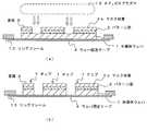
本発明の製造方法の実施形態を図1〜図6を参照して説明する。半導体ウェハ1は、その表面Sに半導体素子の回路などが形成されたパターン面2を有している(図1(a)参照)。半導体ウェハ1のパターン面2側には、マスク一体型表面保護テープ3が貼合される(図1(b)参照)。以上により、パターン面2がマスク一体型表面保護テープ3で被覆された半導体ウェハ1が得られる(図1(c)参照)。 An embodiment of the manufacturing method of the present invention will be described with reference to FIGS. The semiconductor wafer 1 has a pattern surface 2 on a surface S of which a circuit of a semiconductor element is formed (see FIG. 1A). A mask-integrated surface protection tape 3 is bonded to the pattern surface 2 side of the semiconductor wafer 1 (see FIG. 1B). Thus, the semiconductor wafer 1 having the pattern surface 2 covered with the mask-integrated surface protection tape 3 is obtained (see FIG. 1C).
なお、マスク一体型表面保護テープ3は、基材フィルム3aaに粘着剤層3abを設けた表面保護テープ3aの粘着剤層3ab上に、さらにマスク材層3bが設けられて構成される。すなわち、マスク一体型表面保護テープ3は、表面保護テープ3aと、表面保護テープ3a上に設けられたマスク材層3bとを有する。なお、マスク一体型表面保護テープ3において、基材フィルム3aa、粘着剤層3ab、マスク材層3bは、それぞれ単層構造でも2層以上の複層構造でもよい。粘着剤層3ab及びマスク材層3bは好ましくは単層構造である。また、マスク材層3b自体の粘着力を利用可能であれば、粘着剤層3abは、必ずしも必要ではない。 The mask-integrated surface protection tape 3 is configured such that a mask material layer 3b is further provided on the adhesive layer 3ab of the surface protection tape 3a in which the adhesive layer 3ab is provided on the base film 3aa. That is, the mask-integrated surface protection tape 3 has a surface protection tape 3a and a mask material layer 3b provided on the surface protection tape 3a. In the mask-integrated surface protection tape 3, the base film 3aa, the pressure-sensitive adhesive layer 3ab, and the mask material layer 3b may each have a single-layer structure or a multilayer structure of two or more layers. The pressure-sensitive adhesive layer 3ab and the mask material layer 3b preferably have a single-layer structure. The adhesive layer 3ab is not necessarily required as long as the adhesive force of the mask material layer 3b itself can be used.
次に、半導体ウェハ1の裏面Bをウェハ研削装置12で研削し、半導体ウェハ1の厚みを薄くする(図2(a)参照)。その研削した裏面Bにはウェハ固定テープ4を貼り合わせて(図2(b)参照)、半導体ウェハ1をリングフレーム13に支持固定する(図2(c)参照)。 Next, the back surface B of the semiconductor wafer 1 is ground by the wafer grinding device 12 to reduce the thickness of the semiconductor wafer 1 (see FIG. 2A). A wafer fixing tape 4 is attached to the ground back surface B (see FIG. 2B), and the semiconductor wafer 1 is supported and fixed to the ring frame 13 (see FIG. 2C).
次に、半導体ウェハ1からマスク一体型表面保護テープ3の表面保護テープ3aを剥離するとともに、そのマスク材層3bは半導体ウェハ1に残して(図3(a)参照)、マスク材層3bを露出させる(図3(b)参照)。そして、表面Sの側からパターン面2に格子状等に適宜形成された複数のストリート(図示せず)に対してCO2レーザーLを照射して、マスク材層3bの、半導体ウェハ1のストリートに相当する部分を除去し、半導体ウェハ1のストリートを開口する(図3(c)参照)。Next, the surface protection tape 3a of the mask-integrated surface protection tape 3 is peeled from the semiconductor wafer 1, and the mask material layer 3b is left on the semiconductor wafer 1 (see FIG. 3A), and the mask material layer 3b is removed. It is exposed (see FIG. 3B). Then, a plurality of streets (not shown) appropriately formed in a lattice shape or the like on the pattern surface 2 from the side of the front surface S is irradiated with a CO2 laser L, and the streets of the semiconductor material 1 of the mask material layer 3b are removed. Is removed, and the streets of the semiconductor wafer 1 are opened (see FIG. 3C).
次に、表面S側から、SF6ガスプラズマ15を照射することにより、ストリート部分で剥き出しになった半導体ウェハ1をエッチングし(図4(a)参照)、個々の半導体のチップ7に分割して個片化する(プラズマダイシング工程)(図4(b)参照)。Next, by irradiating SF6 gas plasma 15 from the surface S side, the semiconductor wafer 1 exposed at the street portion is etched (see FIG. 4A), and divided into individual semiconductor chips 7. Into individual pieces (plasma dicing step) (see FIG. 4B).
ここで、SF6ガスを用いた半導体ウェハのSiのエッチングプロセスはBOSCHプロセスとも呼ばれ、露出したSiと、SF6をプラズマ化して生成したF原子とを反応させ、四フッ化ケイ素(SiF4)として除去するものであり、リアクティブイオンエッチング(RIE)とも呼ばれる。Here, the etching process of Si on a semiconductor wafer using SF6 gas is also called a BOSCH process, and the exposed Si reacts with F atoms generated by converting SF6 into plasma to form silicon tetrafluoride (SiF4). ) And is also called reactive ion etching (RIE).
次いで、マスク材層3bの表面S側から、剥離テープ16を貼り合せる(図5(a)参照)。剥離テープ16は、基材フィルム16aに粘着剤層16bを設けられて構成される。なお、剥離テープ16において、基材フィルム16a、粘着剤層16bは、それぞれ単層構造でも2層以上の複層構造でもよい。粘着剤層16bは好ましくは単層構造である。 Next, a release tape 16 is attached from the surface S side of the mask material layer 3b (see FIG. 5A). The release tape 16 is configured by providing a pressure-sensitive adhesive layer 16b on a base film 16a. In the release tape 16, the base film 16a and the pressure-sensitive adhesive layer 16b may each have a single-layer structure or a multilayer structure of two or more layers. The pressure-sensitive adhesive layer 16b preferably has a single-layer structure.
剥離テープ16は、放射線硬化型の樹脂からなることが望ましい。この場合には、剥離テープ16をマスク材層3bに貼り合せた後、紫外線(UV19)を照射して剥離テープ16を硬化させる(図5(b)参照)。 The release tape 16 is desirably made of a radiation-curable resin. In this case, after bonding the release tape 16 to the mask material layer 3b, the release tape 16 is cured by irradiating ultraviolet rays (UV 19) (see FIG. 5B).
なお、本発明において、剥離テープ16が放射線硬化型の樹脂からなるとは、剥離テープ16の少なくとも一部の構成が放射線硬化型の樹脂からなることを含み、例えば、剥離テープ16の粘着剤層16bのみが放射線硬化型の樹脂からなることも含む。この場合には、剥離テープ16を硬化させるとは、剥離テープ16の粘着剤層16bを硬化させることを意味する。なお、本明細書において「放射線」とは紫外線のような光線や電子線のような電離性放射線の双方を含む意味に用いる、本発明に用いる放射線は紫外線が好ましい。また、剥離テープ16が放射線硬化型の樹脂ではない場合には、剥離テープ16へのUV19照射工程は不要である。 In the present invention, the phrase that the release tape 16 is made of a radiation-curable resin includes that at least a part of the configuration of the release tape 16 is made of a radiation-curable resin. For example, the adhesive layer 16b of the release tape 16 Only that it is composed of a radiation-curable resin. In this case, curing the release tape 16 means curing the adhesive layer 16b of the release tape 16. In the present specification, the term “radiation” is used to include both light rays such as ultraviolet rays and ionizing radiations such as electron beams. The radiation used in the present invention is preferably ultraviolet rays. When the release tape 16 is not a radiation-curable resin, the step of irradiating the release tape 16 with UV 19 is unnecessary.
剥離テープ16を貼り合せて硬化させた後、剥離テープ16をマスク材層3bとともに剥離する(図5(c)参照)。すなわち、マスク材層3bを剥離テープ16に接着させて、マスク材層3bをパターン面2から剥離・除去する。この際、剥離テープ16(粘着剤層16b)へUV19を照射して硬化させることで、剥離前に剥離テープ16が硬化収縮し、この収縮によって、剥離テープ16とマスク材層3bとの界面の凹凸形状が噛み合い、マスク材層3bと剥離テープ16との接着力(剥離強度)を高め、マスク材層3bを確実に剥離・除去することができる。 After the release tape 16 is bonded and cured, the release tape 16 is released together with the mask material layer 3b (see FIG. 5C). That is, the mask material layer 3b is adhered to the release tape 16, and the mask material layer 3b is peeled and removed from the pattern surface 2. At this time, the release tape 16 (the pressure-sensitive adhesive layer 16b) is irradiated with UV 19 to be cured, whereby the release tape 16 cures and contracts before peeling. The irregularities mesh with each other, so that the adhesive force (peeling strength) between the mask material layer 3b and the release tape 16 is increased, and the mask material layer 3b can be reliably peeled and removed.
なお、このようにマスク材層3bを確実に剥離するためには、マスク材層3bと剥離テープ16(粘着剤層16b)との接着力(剥離強度)が十分に高い必要がある。一方で、表面保護テープ3aを剥離する際には、マスク材層3bは、半導体ウェハ1に残る必要がある。したがって、剥離テープ16を剥離する際の、マスク材層3bと剥離テープ16との接着力(剥離強度)は、マスク材層3bと半導体ウェハ1との接着力よりも高く、マスク材層3bと半導体ウェハ1との接着力は、表面保護テープ3aを剥離する際のマスク材層3bと表面保護テープ3aとの接着力よりも高い必要がある。 In order to reliably peel off the mask material layer 3b, the adhesive strength (peel strength) between the mask material layer 3b and the release tape 16 (adhesive layer 16b) needs to be sufficiently high. On the other hand, when peeling off the surface protection tape 3a, the mask material layer 3b needs to remain on the semiconductor wafer 1. Therefore, the adhesive force (peeling strength) between the mask material layer 3b and the peeling tape 16 when the peeling tape 16 is peeled is higher than the adhesive force between the mask material layer 3b and the semiconductor wafer 1, and The adhesive strength to the semiconductor wafer 1 needs to be higher than the adhesive strength between the mask material layer 3b and the surface protection tape 3a when the surface protection tape 3a is peeled off.
ここで、各部の接着力は、例えば、剥離力試験(JIS Z0237)などで評価することができる。また、マスク材層3bと剥離テープ16との接着力や、マスク材層3bと表面保護テープ3aとの接着力は、例えば、粘着剤層3abと粘着剤層16bのそれぞれの構成するポリマーの官能基や鎖長を変えることによって調整することができる。 Here, the adhesive strength of each part can be evaluated by, for example, a peeling force test (JIS Z0237). Further, the adhesive force between the mask material layer 3b and the release tape 16 and the adhesive force between the mask material layer 3b and the surface protection tape 3a are determined, for example, by the functional properties of the respective polymers of the adhesive layer 3ab and the adhesive layer 16b. It can be adjusted by changing the group and the chain length.
剥離テープ16が放射線硬化型粘着剤で構成される場合、アクリル系粘着剤と放射線重合性化合物とを含有してなる粘着剤を好適に用いることができる。アクリル系粘着剤は、(メタ)アクリル系共重合体、あるいは(メタ)アクリル系共重合体と硬化剤との混合物である。(メタ)アクリル系共重合体は、例えば(メタ)アクリル酸エステルを構成成分として有する共重合体、あるいは(メタ)アクリル酸エステルを構成成分として有する2種以上の共重合体の混合物等が挙げられる。これらの共重合体の重量平均分子量は、通常は30万〜100万程度である。(メタ)アクリル系共重合体の全モノマー成分中、(メタ)アクリル酸エステル成分の割合は70モル%以上が好ましく、80モル%以上がより好ましく、90モル%以上がさらに好ましい。 When the release tape 16 is composed of a radiation-curable pressure-sensitive adhesive, a pressure-sensitive adhesive containing an acrylic pressure-sensitive adhesive and a radiation-polymerizable compound can be suitably used. The acrylic pressure-sensitive adhesive is a (meth) acrylic copolymer or a mixture of a (meth) acrylic copolymer and a curing agent. The (meth) acrylic copolymer is, for example, a copolymer having (meth) acrylate as a constituent, or a mixture of two or more copolymers having (meth) acrylate as a constituent. Can be The weight average molecular weight of these copolymers is usually about 300,000 to 1,000,000. The proportion of the (meth) acrylate component in all the monomer components of the (meth) acrylic copolymer is preferably at least 70 mol%, more preferably at least 80 mol%, even more preferably at least 90 mol%.
また、(メタ)アクリル系共重合体のモノマー成分中、(メタ)アクリル酸エステル成分の割合が100モル%でない場合、残部のモノマー成分は(メタ)アクリロイル基を重合性基として重合した形態で存在するモノマー成分((メタ)アクリル酸由来の構成成分等)であることが好ましい。また、(メタ)アクリル系共重合体の全モノマー成分中、後述する硬化剤と反応する官能基(例えばヒドロキシ基)を有する(メタ)アクリル酸エステル成分の割合は、1モル%以上が好ましく、2モル%以上がより好ましく、5モル%以上がより好ましく、10モル%以上がより好ましい。また当該(メタ)アクリル酸エステル成分の割合は35モル%以下が好ましく、25モル%以下がより好ましい。また、(メタ)アクリル系共重合体の全モノマー成分中、後述する硬化剤と反応する官能基(例えばヒドロキシ基)を有する構成成分(モノマー成分)の割合は、5モル%以上が好ましく、10モル%以上がより好ましい。当該割合の上限値は35モル%以下が好ましく、25モル%以下がより好ましい。 When the proportion of the (meth) acrylate component in the monomer component of the (meth) acrylic copolymer is not 100 mol%, the remaining monomer component is formed by polymerizing a (meth) acryloyl group as a polymerizable group. It is preferably an existing monomer component (such as a component derived from (meth) acrylic acid). Further, in all the monomer components of the (meth) acrylic copolymer, the proportion of the (meth) acrylate component having a functional group (for example, a hydroxy group) that reacts with a curing agent described later is preferably 1 mol% or more, 2 mol% or more is more preferable, 5 mol% or more is more preferable, and 10 mol% or more is more preferable. Further, the ratio of the (meth) acrylic acid ester component is preferably 35 mol% or less, more preferably 25 mol% or less. In addition, the proportion of a component (monomer component) having a functional group (for example, a hydroxy group) that reacts with a curing agent described later is preferably 5 mol% or more, among all the monomer components of the (meth) acrylic copolymer. Mole% or more is more preferable. The upper limit of the ratio is preferably 35 mol% or less, more preferably 25 mol% or less.
上記(メタ)アクリル酸エステル成分は、(メタ)アクリル酸アルキルエステル(アルキル(メタ)アクリレートともいう)であることが好ましい。この(メタ)アクリル酸アルキルエステルを構成するアルキル基の炭素数は、1〜20が好ましく、1〜15がより好ましく、1〜12がさらに好ましい。 The (meth) acrylate component is preferably an alkyl (meth) acrylate (also referred to as an alkyl (meth) acrylate). The carbon number of the alkyl group constituting the alkyl (meth) acrylate is preferably 1 to 20, more preferably 1 to 15, and still more preferably 1 to 12.
硬化剤は、(メタ)アクリル系共重合体が有する官能基と反応させて粘着力及び凝集力を調整するために用いられるものである。例えば、1,3−ビス(N,N−ジグリシジルアミノメチル)シクロヘキサン、1,3−ビス(N,N−ジグリシジルアミノメチル)トルエン、1,3−ビス(N,N−ジグリシジルアミノメチル)ベンゼン、N,N,N,N’−テトラグリシジル−m−キシレンジアミンなどの分子中に2個以上のエポキシ基を有するエポキシ化合物、2,4−トリレンジイソシアネート、2,6−トリレンジイソシアネート、1,3−キシリレンジイソシアネート、1,4−キシレンジイソシアネート、ジフェニルメタン−4,4’−ジイソシアネートなどの分子中に2個以上のイソシアネート基を有するイソシアネート系化合物、テトラメチロール−トリ−β−アジリジニルプロピオネート、トリメチロール−トリ−β−アジリジニルプロピオネート、トリメチロールプロパン−トリ−β−アジリジニルプロピオネート、トリメチロールプロパン−トリ−β−(2−メチルアジリジン)プロピオネートなどの分子中に2個以上のアジリジニル基を有するアジリジン系化合物等が挙げられる。硬化剤の添加量は、所望の粘着力に応じて調整すればよく、(メタ)アクリル系共重合体100質量部に対して0.1〜5.0質量部が適当である。本発明に用いる剥離テープ16において、硬化剤は(メタ)アクリル系共重合体と反応した状態にある。 The curing agent is used to react with the functional group of the (meth) acrylic copolymer to adjust the adhesive strength and cohesive strength. For example, 1,3-bis (N, N-diglycidylaminomethyl) cyclohexane, 1,3-bis (N, N-diglycidylaminomethyl) toluene, 1,3-bis (N, N-diglycidylaminomethyl) ) Epoxy compounds having two or more epoxy groups in a molecule, such as benzene, N, N, N, N'-tetraglycidyl-m-xylenediamine, 2,4-tolylenediisocyanate, 2,6-tolylenediisocyanate , 1,3-xylylene diisocyanate, 1,4-xylylene diisocyanate, diphenylmethane-4,4'-diisocyanate, etc., an isocyanate compound having two or more isocyanate groups in a molecule, tetramethylol-tri-β-aziridini Rupropionate, trimethylol-tri-β-aziridinyl propionate, Aziridine compounds having two or more aziridinyl groups in a molecule, such as rimethylolpropane-tri-β-aziridinylpropionate, trimethylolpropane-tri-β- (2-methylaziridine) propionate, and the like. . The amount of the curing agent to be added may be adjusted according to the desired adhesive strength, and is suitably 0.1 to 5.0 parts by mass based on 100 parts by mass of the (meth) acrylic copolymer. In the release tape 16 used in the present invention, the curing agent is in a state of reacting with the (meth) acrylic copolymer.
上記放射線重合性化合物としては、放射線の照射によって三次元網状化しうる、分子内に光重合性炭素−炭素二重結合を少なくとも2個以上有する低分量化合物が広く用いられる。具体的には、トリメチロールプロパントリアクリレート、テトラメチロールメタンテトラアクリレート、ペンタエリスリトールトリアクリレート、ペンタエリスリトールテトラアクリレート、ジペンタエリスリトールモノヒドロキシペンタアクリレート、ジペンタエリスリトールヘキサアクリレート、1,4−ブチレングリコールジアクリレート、1,6−ヘキサンジオールジアクリレート、ポリエチレングリコールジアクリレートや、オリゴエステルアクリレート等のアクリレート系化合物を広く適用可能である。 As the radiation polymerizable compound, a low-quantity compound having at least two or more photopolymerizable carbon-carbon double bonds in a molecule, which can be formed into a three-dimensional network by irradiation with radiation, is widely used. Specifically, trimethylol propane triacrylate, tetramethylol methane tetraacrylate, pentaerythritol triacrylate, pentaerythritol tetraacrylate, dipentaerythritol monohydroxypentaacrylate, dipentaerythritol hexaacrylate, 1,4-butylene glycol diacrylate, Acrylate compounds such as 1,6-hexanediol diacrylate, polyethylene glycol diacrylate, and oligoester acrylate can be widely applied.
また、上記アクリレート系化合物のほかに、ウレタンアクリレート系オリゴマーを用いる事も出来る。ウレタンアクリレート系オリゴマーは、ポリエステル型またはポリエーテル型などのポリオール化合物と、多価イソシアナート化合物(例えば、2,4−トリレンジイソシアナート、2,6−トリレンジイソシアナート、1,3−キシリレンジイソシアナート、1,4−キシリレンジイソシアナート、ジフェニルメタン4,4−ジイソシアナートなど)を反応させて得られる末端イソシアナートウレタンプレポリマーに、ヒドロキシ基を有するアクリレートあるいはメタクリレート(例えば、2−ヒドロキシエチルアクリレート、2−ヒドロキシエチルメタクリレート、2−ヒドロキシプロピルアクリレート、2−ヒドロキシプロピルメタクリレート、ポリエチレングリコールアクリレート、ポリエチレングリコールメタクリレートなど)を反応させて得られる。 In addition to the above acrylate compounds, urethane acrylate oligomers can also be used. The urethane acrylate oligomer includes a polyol compound such as a polyester type or a polyether type, and a polyvalent isocyanate compound (for example, 2,4-tolylene diisocyanate, 2,6-tolylene diisocyanate, 1,3-xylylylene). Isocyanate, 1,4-xylylene diisocyanate, diphenylmethane 4,4-diisocyanate, etc.), and a terminal isocyanate urethane prepolymer obtained by reaction with acrylate or methacrylate having a hydroxy group (for example, 2-hydroxyethyl). Acrylate, 2-hydroxyethyl methacrylate, 2-hydroxypropyl acrylate, 2-hydroxypropyl methacrylate, polyethylene glycol acrylate, polyethylene glycol methacrylate, etc.) Obtained by response.
放射線硬化型粘着剤中のアクリル系粘着剤と放射線重合性化合物との配合比としては、アクリル系粘着剤100質量部に対して放射線重合性化合物を50〜200質量部、好ましくは50〜150質量部の範囲で配合されるのが望ましい。この配合比の範囲である場合、剥離テープ16の粘着力を大きく低下させることが可能となる。 As the compounding ratio of the acrylic pressure-sensitive adhesive and the radiation-polymerizable compound in the radiation-curable pressure-sensitive adhesive, the radiation-polymerizable compound is 50 to 200 parts by mass, preferably 50 to 150 parts by mass, based on 100 parts by mass of the acrylic pressure-sensitive adhesive. It is desirable to mix in the range of parts. When the mixing ratio is within the range, the adhesive strength of the release tape 16 can be significantly reduced.
また、剥離テープ16に用いる放射線硬化型粘着剤として、上記(メタ)アクリル系共重合体自体を放射線重合性とした、放射線重合性(メタ)アクリル系共重合体を用いることも好ましい。この場合において、放射線硬化型粘着剤は硬化剤を含んでいてもよい。 Further, as the radiation-curable pressure-sensitive adhesive used for the release tape 16, it is also preferable to use a radiation-polymerizable (meth) acrylic copolymer in which the (meth) acrylic copolymer itself is made radiation-polymerizable. In this case, the radiation-curable pressure-sensitive adhesive may include a curing agent.
放射線重合性(メタ)アクリル系共重合体は、共重合体の分子中に、放射線、特に紫外線照射で重合反応することが可能な反応性の基を有する共重合体である。このような反応性の基としては、エチレン性不飽和基、すなわち、炭素−炭素二重結合を有する基が好ましい。かかる基の例として、ビニル基、アリル基、スチリル基、(メタ)アクリロイルオキシ基、(メタ)アクリロイルアミノ基などが挙げられる。 The radiation polymerizable (meth) acrylic copolymer is a copolymer having a reactive group capable of undergoing a polymerization reaction by irradiation with radiation, particularly ultraviolet light, in the molecule of the copolymer. As such a reactive group, an ethylenically unsaturated group, that is, a group having a carbon-carbon double bond is preferable. Examples of such groups include vinyl, allyl, styryl, (meth) acryloyloxy, and (meth) acryloylamino groups.
上記反応性基の共重合体中への導入は、例えば、ヒドロキシ基を有する共重合体と、ヒドロキシ基と反応する基(例えば、イソシアネート基)を有し、かつ上記反応性基を有する化合物(代表的には、2−(メタ)アクリロイルオキシエチルイソシアネート)とを反応させることにより行うことができる。 The introduction of the reactive group into the copolymer may be, for example, a copolymer having a hydroxy group and a compound having a group that reacts with the hydroxy group (for example, an isocyanate group) and having the reactive group ( Typically, the reaction can be carried out by reacting 2- (meth) acryloyloxyethyl isocyanate).
また、上記放射線重合性(メタ)アクリル系共重合体を構成する全モノマー成分中、上記の反応性の基を有するモノマー成分の割合は2〜40モル%が好ましく、5〜30モル%がより好ましく、10〜30モル%がさらに好ましい。 In addition, the proportion of the monomer component having a reactive group is preferably 2 to 40 mol%, and more preferably 5 to 30 mol%, of all the monomer components constituting the radiation-polymerizable (meth) acrylic copolymer. Preferably, 10 to 30 mol% is more preferable.
また、放射線により剥離テープ16を重合硬化させる場合には、光重合開始剤、例えばイソプロピルベンゾインエーテル、イソブチルベンゾインエーテル、ベンゾフェノン、ミヒラーズケトン、クロロチオキサントン、ベンジルメチルケタール、α−ヒドロキシシクロヘキシルフェニルケトン、2−ヒドロキシメチルフェニルプロパン等を用いることが出来る。これらのうち少なくとも1種類を剥離テープ16に添加することにより、効率よく重合反応を進行させることが出来る。 When the release tape 16 is polymerized and cured by radiation, a photopolymerization initiator such as isopropyl benzoin ether, isobutyl benzoin ether, benzophenone, Michler's ketone, chlorothioxanthone, benzyl methyl ketal, α-hydroxycyclohexyl phenyl ketone, 2-hydroxy Methylphenylpropane or the like can be used. By adding at least one of these to the release tape 16, the polymerization reaction can proceed efficiently.
上記剥離テープ16は、さらに光増感剤、従来公知の粘着付与剤、軟化剤、酸化防止剤等を含有していてもよい。 The release tape 16 may further contain a photosensitizer, a conventionally known tackifier, a softener, an antioxidant, and the like.
以上により、表面Sに残ったマスク材層3bが取り除かれる(図6(a)参照)。そして最後に個片化されたチップ7をピン17により突き上げコレット18により吸着してピックアップする(図6(b)参照)。以上により、半導体チップを製造することができる。 Thus, the mask material layer 3b remaining on the surface S is removed (see FIG. 6A). Then, the chips 7 finally separated are pushed up by the pins 17 and are sucked and picked up by the collet 18 (see FIG. 6B). As described above, a semiconductor chip can be manufactured.
次に、本発明の製造方法で用いる材料について説明する。半導体ウェハ1は、片面に半導体素子の回路などが形成されたパターン面2を有するシリコンウェハなどであり、パターン面2は、半導体素子の回路などが形成された面であって、平面視においてストリートを有する。 Next, the materials used in the production method of the present invention will be described. The semiconductor wafer 1 is, for example, a silicon wafer having a pattern surface 2 on which a circuit of a semiconductor element is formed on one surface. The pattern surface 2 is a surface on which a circuit of the semiconductor element is formed, and has a street shape in plan view. Having.
(マスク一体型表面保護テープ3)
マスク一体型表面保護テープ3は、基材フィルム3aa上に粘着剤層3abが設けられ、さらに粘着剤層3ab上にマスク材層3bが設けられた構成を有し、パターン面2に形成された半導体素子を保護する機能を有する。即ち、後工程のウェハ薄膜化工程ではパターン面2で半導体ウェハ1を支持してウェハの裏面が研削されるために、この研削時の負荷に耐える必要がある。そのため、マスク一体型表面保護テープ3は単なるレジスト膜等とは異なり、パターン面2に形成される素子を被覆するだけの厚みがあって、その押圧抵抗は低く、また研削時のダストや研削水などの浸入が起こらないように素子を密着できるだけの密着性が高いものである。(Mask integrated surface protection tape 3)
The mask-integrated surface protection tape 3 has a configuration in which an adhesive layer 3ab is provided on a base film 3aa, and a mask material layer 3b is further provided on the adhesive layer 3ab, and is formed on the pattern surface 2. It has a function of protecting a semiconductor element. That is, in the subsequent wafer thinning step, since the semiconductor wafer 1 is supported on the pattern surface 2 and the back surface of the wafer is ground, it is necessary to withstand the load during the grinding. Therefore, the mask-integrated surface protection tape 3 is different from a mere resist film or the like in that it has a thickness enough to cover the elements formed on the pattern surface 2, has a low pressing resistance, and has a small dust or grinding water during grinding. It has a high degree of adhesion that allows the elements to be in close contact with each other so that no intrusion occurs.
(基材フィルム3aa)
マスク一体型表面保護テープ3のうち基材フィルム3aaはプラスチックやゴム等からなり、例えばポリエチレン、ポリプロピレン、エチレン−プロピレン共重合体、ポリブテン−1、ポリ−4−メチルペンテン−1、エチレン−酢酸ビニル共重合体、エチレン−アクリル酸共重合体、アイオノマー等のα−オレフィンの単独重合体または共重合体、あるいはこれらの混合物、ポリエチレンテレフタレート、ポリエチレンナフタレート、ポリフェニレンサルファイド、ポリエーテルイミド、ポリイミド、ポリカーボネート、ポリメチルメタクリレート、ポリウレタン、スチレン−エチレン−ブテン−もしくはペンテン系共重合体等の単体もしくは2種以上を混合させたもの、さらにこれらにこれら以外の樹脂や充填材、添加剤等が配合された樹脂組成物をその材質として挙げることができ、要求特性に応じて適宜に選ぶことができる。低密度ポリエチレンとエチレン酢酸ビニル共重合体の積層体や、ポリプロピレンとポリエチレンテレフタレートの積層体、ポリエチレンテレフタレート、ポリエチレンナフタレートは好適な材質の一つである。(Base film 3aa)
The base film 3aa of the mask-integrated surface protection tape 3 is made of plastic, rubber, or the like. For example, polyethylene, polypropylene, ethylene-propylene copolymer, polybutene-1, poly-4-methylpentene-1, ethylene-vinyl acetate Copolymer, ethylene-acrylic acid copolymer, homopolymer or copolymer of α-olefin such as ionomer, or a mixture thereof, polyethylene terephthalate, polyethylene naphthalate, polyphenylene sulfide, polyetherimide, polyimide, polycarbonate, Polymethyl methacrylate, polyurethane, styrene-ethylene-butene- or pentene-based copolymers alone or in a mixture of two or more, and further mixed with other resins, fillers, additives, and the like. It can be mentioned fat composition as the material can be selected appropriately in accordance with required characteristics. A laminate of low-density polyethylene and ethylene-vinyl acetate copolymer, a laminate of polypropylene and polyethylene terephthalate, polyethylene terephthalate, and polyethylene naphthalate are one of suitable materials.
これらの基材フィルム3aaは、一般的な押出し法を用いて製造できる。基材フィルム3aaを種々の樹脂を積層して得る場合には、共押出し法、ラミネート法などで製造される。この際、通常のラミネートフィルムの製法に於いて普通に行われている様に、樹脂と樹脂の間に接着層を設けても良い。この様な基材フィルム3aaの厚さは、強度、伸度等の特性、放射線透過性の観点から20〜200μmが好ましい。 These base films 3aa can be manufactured using a general extrusion method. When the base film 3aa is obtained by laminating various resins, it is manufactured by a co-extrusion method, a lamination method, or the like. At this time, an adhesive layer may be provided between the resins, as is generally performed in a normal method of manufacturing a laminated film. The thickness of such a base film 3aa is preferably 20 to 200 μm from the viewpoints of properties such as strength and elongation and radiation transmittance.
(粘着剤層3ab)
粘着剤層3abは、マスク材層3bと共に、パターン面2に形成される素子の凹凸を吸収してパターン面2との密着性を高め、パターン面2を保護する役割を担う。マスク一体型表面保護テープ3をウェハ薄膜化工程(裏面研削工程)の負荷に耐えるものとするために、ウェハ薄膜化工程においては、粘着剤層3abと、マスク材層3bないし基材フィルム3aaとの密着性が高いことが好ましい。一方、ウェハ薄膜化工程後においては、基材フィルム3aaと一体となってマスク材層3bと剥離されるために、粘着剤層3abとマスク材層3bとの密着性は低いことが好ましい(剥離性が高いことが好ましい)。(Adhesive layer 3ab)
The pressure-sensitive adhesive layer 3ab, together with the mask material layer 3b, plays a role of absorbing the unevenness of the element formed on the pattern surface 2, increasing the adhesion to the pattern surface 2, and protecting the pattern surface 2. In order to make the mask-integrated surface protection tape 3 withstand the load of the wafer thinning step (backside grinding step), in the wafer thinning step, the adhesive layer 3ab, the mask material layer 3b or the base film 3aa, Is preferably high in adhesion. On the other hand, after the wafer thinning step, the adhesiveness between the pressure-sensitive adhesive layer 3ab and the mask material layer 3b is preferably low because the mask material layer 3b is peeled off integrally with the base film 3aa (separation). It is preferred that the property is high).
なお、本発明において粘着剤層3abは、所望の特性を有する範囲で非放射線硬化型の粘着剤(感圧型粘着剤)を適用可能である。 In the present invention, a non-radiation-curable pressure-sensitive adhesive (pressure-sensitive pressure-sensitive adhesive) can be applied to the pressure-sensitive adhesive layer 3ab within a range having desired characteristics.
粘着剤層3abの厚さは、パターン面2に形成された素子等の保護能をより高め、またパターン面2への密着性をより高める観点から、5〜100μmが好ましく、10〜100μmがより好ましく、2〜50μmがさらに好ましい。なお、デバイスの種類にもよるが、パターン表面の凹凸は概ね数μm〜15μm程度であるため、粘着剤層3abの厚さは5〜30μmがより好ましい。 The thickness of the pressure-sensitive adhesive layer 3ab is preferably from 5 to 100 μm, more preferably from 10 to 100 μm, from the viewpoint of further improving the protective ability of the element and the like formed on the pattern surface 2 and further improving the adhesion to the pattern surface 2. Preferably, it is more preferably 2 to 50 μm. In addition, although it depends on the type of the device, the unevenness of the pattern surface is generally about several μm to 15 μm, and thus the thickness of the pressure-sensitive adhesive layer 3ab is more preferably 5 to 30 μm.
(マスク材層3b)
マスク材層3bは、パターン面2への貼着に際し半導体素子等を傷つけにくく、また、その除去の際に半導体素子等の破損や表面への粘着剤残留を生じにくいものである。マスク材層3bとしては、好ましくは放射線、より好ましくは紫外線照射によりマスク材層3bが三次元網状化を呈し、紫外線硬化型、あるいは電子線のような電離性放射線硬化型等の放射線重合型のマスク材層3bを用いることができる。(Mask material layer 3b)
The mask material layer 3b does not easily damage the semiconductor element or the like when sticking to the pattern surface 2, and hardly causes damage to the semiconductor element or the like and residue of the adhesive on the surface when the semiconductor element or the like is removed. As the mask material layer 3b, preferably, the mask material layer 3b exhibits a three-dimensional network by irradiation with radiation, more preferably ultraviolet light, and is a radiation polymerizable type such as an ultraviolet curable type or an ionizing radiation curable type such as an electron beam. The mask material layer 3b can be used.
また、非放射線硬化型である、いわゆる感圧型の粘着剤も好適に用いられる。この感圧型の粘着剤としては、上述した、(メタ)アクリル系共重合体と硬化剤との混合物を好適に用いることができる。 Also, a non-radiation-curable, so-called pressure-sensitive adhesive is suitably used. As the pressure-sensitive adhesive, the above-described mixture of the (meth) acrylic copolymer and the curing agent can be suitably used.
こうしたマスク材層3bとしては、アクリル系粘着剤や、このアクリル系粘着剤と放射線重合性化合物とを含有してなるマスク材を好適に用いることができる。上記アクリル系粘着剤は、(メタ)アクリル系共重合体、あるいは(メタ)アクリル系共重合体と硬化剤との混合物であり、前述の剥離テープ16で記載するアクリル系粘着剤を好適に用いることができる。なお、密着性の観点から、(メタ)アクリル系共重合体の全モノマー成分中、硬化剤と反応する官能基(例えば、ヒドロキシ基)を有する(メタ)アクリル酸エステル成分の割合は、0.1モル%以上が好ましく、0.5モル%以上がより好ましい。上限値は、20モル%以下であることが好ましく、15モル%以下であることがより好ましい。(メタ)アクリル系共重合体の質量平均分子量は、10万〜100万程度が好ましい。 As the mask material layer 3b, an acrylic pressure-sensitive adhesive or a mask material containing the acrylic pressure-sensitive adhesive and a radiation polymerizable compound can be suitably used. The acrylic pressure-sensitive adhesive is a (meth) acrylic copolymer or a mixture of a (meth) acrylic copolymer and a curing agent, and preferably uses the acrylic pressure-sensitive adhesive described in the release tape 16 described above. be able to. From the viewpoint of adhesion, the proportion of the (meth) acrylate component having a functional group (for example, a hydroxy group) that reacts with the curing agent in all the monomer components of the (meth) acrylic copolymer is 0.1%. It is preferably at least 1 mol%, more preferably at least 0.5 mol%. The upper limit is preferably at most 20 mol%, more preferably at most 15 mol%. The mass average molecular weight of the (meth) acrylic copolymer is preferably about 100,000 to 1,000,000.
前述したように、マスク材層3bとしては、放射線で硬化する放射線硬化型粘着剤や、放射線で硬化しない感圧型粘着剤を好適に用いることができる。上記放射線硬化型粘着剤としては、上記アクリル系粘着剤と、分子内に1または2個の光重合性炭素−炭素二重結合を有するアクリレート化合物とを含有してなる粘着剤が好適である。上記放射線硬化型粘着剤中、分子内に1または2個の光重合性炭素−炭素二重結合を有するアクリレート化合物の含有量は15質量%以上が好ましく、15〜70質量%がより好ましく、15〜65質量%がさらに好ましい。また、分子内に1または2個の光重合性炭素−炭素二重結合を有するアクリレート化合物は、分子内に1個の光重合性炭素−炭素二重結合を有するアクリレート化合物であることが好ましい。 As described above, as the mask material layer 3b, a radiation-curable pressure-sensitive adhesive that cures with radiation or a pressure-sensitive adhesive that does not cure with radiation can be suitably used. As the radiation-curable pressure-sensitive adhesive, a pressure-sensitive adhesive containing the acrylic pressure-sensitive adhesive and an acrylate compound having one or two photopolymerizable carbon-carbon double bonds in a molecule is preferable. In the radiation-curable pressure-sensitive adhesive, the content of the acrylate compound having one or two photopolymerizable carbon-carbon double bonds in the molecule is preferably 15% by mass or more, more preferably 15 to 70% by mass, and 15% by mass. ~ 65 mass% is more preferred. The acrylate compound having one or two photopolymerizable carbon-carbon double bonds in the molecule is preferably an acrylate compound having one photopolymerizable carbon-carbon double bond in the molecule.
上記分子内に1または2個の光重合性炭素−炭素二重結合を有するアクリレート化合物は、具体的には、2−ヒドロキシ−3−フェノキシプロピルアクリレート、1,4−ブチレングリコールジアクリレート、1,6−ヘキサンジオールジアクリレート、ポリエチレングリコールジアクリレート等を広く適用可能である。また、分子内に1または2個の光重合性炭素−炭素二重結合を有する、ウレタンアクリレートオリゴマーを好適に用いる事ができ、前述の剥離テープ16に記載する方法で得られるウレタンアクリレートオリゴマーを好ましく用いることができる。 The acrylate compound having one or two photopolymerizable carbon-carbon double bonds in the molecule is, specifically, 2-hydroxy-3-phenoxypropyl acrylate, 1,4-butylene glycol diacrylate, 6-hexanediol diacrylate, polyethylene glycol diacrylate and the like are widely applicable. Further, a urethane acrylate oligomer having one or two photopolymerizable carbon-carbon double bonds in the molecule can be suitably used, and the urethane acrylate oligomer obtained by the method described in the release tape 16 is preferably used. Can be used.
上記放射線硬化型粘着剤中のアクリル系粘着剤と、分子内に1または2個の光重合性炭素−炭素二重結合を有するアクリレート化合物との配合比としては、アクリル系粘着剤100質量部に対して、分子内に1または2個の光重合性炭素−炭素二重結合を有するアクリレート化合物を10〜250質量部、好ましくは15〜200質量部の範囲で配合されるのが好ましい。上記上限値以下であると、裏面研削時にマスク材層3bが過度に変形することなく、半導体ウェハ1の破損をより効果的に防止することができる。 The mixing ratio of the acrylic pressure-sensitive adhesive in the radiation-curable pressure-sensitive adhesive and the acrylate compound having one or two photopolymerizable carbon-carbon double bonds in the molecule is 100 parts by mass of the acrylic pressure-sensitive adhesive. On the other hand, it is preferable that an acrylate compound having one or two photopolymerizable carbon-carbon double bonds in a molecule is blended in an amount of 10 to 250 parts by mass, preferably 15 to 200 parts by mass. When the thickness is equal to or less than the upper limit, breakage of the semiconductor wafer 1 can be more effectively prevented without excessively deforming the mask material layer 3b during back surface grinding.
また、マスク材層3bには、前述の剥離テープ16における放射線重合性(メタ)アクリル酸エステル共重合体、光重合開始剤、その他の含有成分(光増感剤、従来公知の粘着付与剤、軟化剤、酸化防止剤等)を好ましく適用することができる。 Further, the mask material layer 3b includes a radiation polymerizable (meth) acrylate copolymer, a photopolymerization initiator, and other components (a photosensitizer, a conventionally known tackifier, Softeners, antioxidants, etc.) can be preferably applied.
本発明のマスク一体型表面保護テープ3において、マスク材層3bの厚さは、パターン面2に形成された素子等の保護能をより高め、またパターン面2への密着性をより高めることでSF6ガスの侵入を防止し、マスク材層3bの除去性をより高める観点から、1〜100μmが好ましく、5〜30μmがより好ましい。なお、デバイスの種類にもよるが、パターン表面の凹凸は概ね数μm〜15μm程度であるため、マスク材層3bの厚さは5〜30μmがより好ましく、さらに5〜20μmがより好ましい。In the mask-integrated surface protection tape 3 of the present invention, the thickness of the mask material layer 3b is set so that the protection ability of the elements and the like formed on the pattern surface 2 is further improved and the adhesion to the pattern surface 2 is further improved. From the viewpoint of preventing intrusion of SF6 gas and further improving the removability of the mask material layer 3b, the thickness is preferably 1 to 100 μm, more preferably 5 to 30 μm. In addition, although it depends on the type of the device, since the unevenness of the pattern surface is approximately several μm to 15 μm, the thickness of the mask material layer 3b is more preferably 5 to 30 μm, and further preferably 5 to 20 μm.
さらに、本発明のマスク一体型表面保護テープ3において、マスク材層3bは、波長10μmでの光線透過率(以下、光線透過率10μmとも称す。)が80%以下であり、波長350〜700nmでの可視光線透過率(以下、可視光線透過率350−700μmとも称す。)が50%以上であることが好ましい。光線透過率10μmは、79%以下であることがより好ましく、75%以下であることがさらに好ましい。下限値の制限は特にないが、30%以上であることが現実的である。可視光線透過率350−700μmは、70%以上であることがより好ましく、90%以上であることがさらに好ましい。上限値の制限は特にないが、100%以下であることが好ましい。Further, in the mask-integrated surface protection tape 3 of the present invention, the mask material layer 3b has a light transmittance at a wavelength of 10 μm (hereinafter also referred to as a light transmittance of10 μm ) of 80% or less, and a wavelength of 350 to 700 nm.Preferably has a visible light transmittance of 50% or more (hereinafter also referred to as a visible light transmittance of350 to700 μm ). The light transmittance of 10 μm is more preferably 79% or less, and further preferably 75% or less. Although there is no particular limitation on the lower limit, it is realistic that it is 30% or more. The visible light transmittance of350 to 700μm is more preferably 70% or more, and further preferably 90% or more. The upper limit is not particularly limited, but is preferably 100% or less.
光線透過率10μmが上記好ましい範囲内にあることで、マスク材層3bのうち、半導体ウェハ1のストリートに相当する部分を、CO2レーザーにより効率的に切断することができる。また、可視光線透過率350−700μmが上記好ましい範囲内にあることで、半導体ウェハ1のパターン面2を適切に認識することができ、ストリート開口する際の誤認識を防止することができる。When the light transmittance is in the range of10 μm , the portion of the mask material layer 3b corresponding to the street of the semiconductor wafer 1 can be efficiently cut by the CO2 laser. Further, when the visible light transmittance is in the range of350 to700 μm, the pattern surface 2 of the semiconductor wafer 1 can be properly recognized, and erroneous recognition at the time of opening a street can be prevented.
なお、光線透過率は、以下のように測定される。まず、マスク一体型表面保護テープ3を、易接着処理したPETフィルムに貼合し表面保護テープ3aのみを剥離する。得られたPETフィルムとマスク材層3bからなる積層体の透過率を、分光光度計(商品名:UV−1800、島津製作所製)で測定し、得られた透過率から、PETフィルム単体の透過率を差し引くことで、マスク材層3bの透過率が算出される。 The light transmittance is measured as follows. First, the mask-integrated surface protection tape 3 is bonded to a PET film that has been subjected to an easy adhesion treatment, and only the surface protection tape 3a is peeled off. The transmittance of the laminate comprising the obtained PET film and the mask material layer 3b was measured with a spectrophotometer (trade name: UV-1800, manufactured by Shimadzu Corporation), and the transmittance of the PET film alone was determined from the obtained transmittance. By subtracting the rate, the transmittance of the mask material layer 3b is calculated.
(剥離テープ16)
剥離テープ16は、マスク材層3bを剥離可能であれば、その材質および構成は問わないが、例えば、基材フィルム16aは、前述した表面保護テープ3aの基材フィルム3aaと同様の物を適用可能である。また、粘着剤層16bは、前述した表面保護テープ3aの粘着剤層3abと同様の物を適用可能である。なお、前述した様に、粘着剤層16bと粘着剤層3abとは、例えば、ポリマー構成成分、モノマー種が異なる。(Release tape 16)
The material and the configuration of the release tape 16 are not limited as long as the mask material layer 3b can be peeled off. For example, the base film 16a is the same as the base film 3aa of the surface protection tape 3a described above. It is possible. Further, the same material as the pressure-sensitive adhesive layer 3ab of the surface protection tape 3a described above can be applied to the pressure-sensitive adhesive layer 16b. As described above, the pressure-sensitive adhesive layer 16b and the pressure-sensitive adhesive layer 3ab differ from each other in, for example, a polymer component and a monomer type.
(ウェハ固定テープ4)
ウェハ固定テープ4は、半導体ウェハ1を保持し、プラズマダイシング工程にさらされても耐えうるプラズマ耐性が必要である。またピックアップ工程においては良好なピックアップ性や場合によってはエキスパンド性等も要求されるものである。こうしたウェハ固定テープ4には、上記表面保護テープ3aと同様のテープを用いることができる。また一般的にダイシングテープと称される従来のプラズマダイシング方式で利用される公知のダイシングテープを用いることができる。また、ピックアップ後のダイボンディング工程への移行を容易にするために、粘着剤層3ab上にダイボンディング用接着剤を積層したダイシングダイボンディングテープを用いることもできる。(Wafer fixing tape 4)
The wafer fixing tape 4 is required to hold the semiconductor wafer 1 and have a plasma resistance that can withstand the plasma dicing process. In the pickup step, good pickup properties and, in some cases, expandability are required. The same tape as the surface protection tape 3a can be used for the wafer fixing tape 4. Further, a known dicing tape generally used in a conventional plasma dicing method called a dicing tape can be used. In order to facilitate the transition to the die bonding step after the pickup, a dicing die bonding tape in which a die bonding adhesive is laminated on the adhesive layer 3ab can be used.
マスク材層3bを切断するレーザーには、紫外線または赤外線のレーザー光を照射するレーザー照射装置を用いることができる。このレーザー照射装置は、半導体ウェハ1のストリートに沿って移動可能にレーザー照射部が配設されており、マスク材層3bを除去するために適切に制御された出力のレーザーLを照射できる。なかでもCO2レーザーは数W〜数十Wの大出力を得ることが可能であり、本発明に好適に利用できる。As a laser for cutting the mask material layer 3b, a laser irradiation device that irradiates ultraviolet or infrared laser light can be used. This laser irradiation device is provided with a laser irradiation unit movably along the street of the semiconductor wafer 1, and can irradiate a laser L with an appropriately controlled output to remove the mask material layer 3b. Above all, the CO2 laser can obtain a large output of several W to several tens of W, and can be suitably used in the present invention.
プラズマダイシングを行うにはプラズマエッチング装置を用いることができる。プラズマエッチング装置は、半導体ウェハ1に対してドライエッチングを行い得る装置であって、真空チャンバ内に密閉処理空間をつくり、高周波側電極に半導体ウェハ1が載置され、その高周波側電極に対向して設けられたガス供給電極側からプラズマ発生用ガスが供給されるものである。高周波側電極に高周波電圧が印加されればガス供給電極と高周波側電極との間にプラズマが発生するため、このプラズマを利用する。発熱する高周波電極内には冷媒を循環させて、プラズマの熱による半導体ウェハ1の昇温を防止している。 For performing plasma dicing, a plasma etching apparatus can be used. The plasma etching apparatus is an apparatus capable of performing dry etching on the semiconductor wafer 1, creates a closed processing space in a vacuum chamber, places the semiconductor wafer 1 on the high frequency side electrode, and faces the high frequency side electrode. The gas for plasma generation is supplied from the gas supply electrode side provided in the above manner. If a high frequency voltage is applied to the high frequency side electrode, plasma is generated between the gas supply electrode and the high frequency side electrode, and this plasma is used. A coolant is circulated in the high-frequency electrode that generates heat to prevent the temperature of the semiconductor wafer 1 from rising due to the heat of the plasma.
上記半導体チップの製造方法(半導体ウェハの処理方法)によれば、パターン面2を保護する表面保護テープ3aにプラズマダイシングにおけるマスク機能を持たせたことで、従来のプラズマダイシングプロセスで用いられていたレジストを設けるためのフォトリソ工程等が不要となる。特に表面保護テープ3aを用いたため、マスクの形成に印刷や転写等の高度な位置合わせが要求される技術が不要で簡単に半導体ウェハ1の表面Sに貼合でき、レーザー装置により簡単にマスクを形成できる。 According to the semiconductor chip manufacturing method (semiconductor wafer processing method), the surface protection tape 3a for protecting the pattern surface 2 is provided with a mask function in plasma dicing, and is used in a conventional plasma dicing process. A photolithography step or the like for providing a resist becomes unnecessary. In particular, since the surface protection tape 3a is used, a technique that requires advanced alignment such as printing and transfer is not required for forming the mask, and the mask can be easily attached to the surface S of the semiconductor wafer 1, and the mask can be easily formed by a laser device. Can be formed.
また、マスク材層3bを剥離テープ16で除去できるため、特殊な装置を使用せずにマスク材層3bを除去することができる。加えてパターン面2側(表面S側)からプラズマダイシングを行うため、ピッキング作業前にチップ7の上下を反転させる必要がない。これらの理由から設備を簡易化でき、プロセスコストを大幅に抑えることができる。 Further, since the mask material layer 3b can be removed with the release tape 16, the mask material layer 3b can be removed without using a special device. In addition, since plasma dicing is performed from the pattern surface 2 side (surface S side), it is not necessary to turn the chip 7 upside down before the picking operation. For these reasons, the equipment can be simplified and the process cost can be greatly reduced.
上記各実施形態は本発明の一例であり、こうした形態に限定されるものではなく、本発明の趣旨に反しない限度において、各プロセスにおける公知のプロセスの付加や削除、変更等を行い得るものである。 Each of the above embodiments is an example of the present invention, and the present invention is not limited to such an embodiment, and may add, delete, or change a known process in each process without departing from the spirit of the present invention. is there.
以下、実施例に基づき本発明をさらに詳細に説明するが、本発明はこれに限定されるものでない。 Hereinafter, the present invention will be described in more detail with reference to Examples, but the present invention is not limited thereto.
(表面保護テープ3a)
構成単位として、ラウリルアクリレート:74mol%、アクリル酸メチル:6mol%、2-ヒドロキシエチルアクリレート:20mol%由来の構成単位を各モル比で有するアクリルポリマーA(Mw:35万、酸価:7mgKOH/g、水酸基価:60mgKOH/g)100質量部に対し、イソシアネート硬化剤(商品名:L‐45、東ソー株式会社製)を1.0質量部配合して粘着剤組成物Aを得た。(Surface protection tape 3a)
Acrylic polymer A (Mw: 350,000, acid value: 7 mgKOH / g) having constitutional units derived from lauryl acrylate: 74 mol%, methyl acrylate: 6 mol%, 2-hydroxyethyl acrylate: 20 mol% as constitutional units in each molar ratio. , Hydroxyl value: 60 mg KOH / g) and 100 parts by mass of an isocyanate curing agent (trade name: L-45, manufactured by Tosoh Corporation) were mixed in an amount of 1.0 part by mass to obtain PSA composition A.
別途、低密度ポリエチレン(LDPE)樹脂(商品名:ニポロンハード205、東ソー株式会社製)とエチレン−酢酸ビニル共重合体(EVA)樹脂(商品名:ウルトラセン540、東ソー株式会社製)からなる基材フィルム3aaを押出法により厚さが110μmとなるように製膜した。 Separately, a base material made of low density polyethylene (LDPE) resin (trade name: Nipolon Hard 205, manufactured by Tosoh Corporation) and ethylene-vinyl acetate copolymer (EVA) resin (trade name: Ultracene 540, manufactured by Tosoh Corporation) The film 3aa was formed into a thickness of 110 μm by an extrusion method.
前記粘着剤組成物Aを、乾燥後の厚さが20μmとなるように前記基材フィルム3aaのEVA樹脂層上に塗布、乾燥して粘着剤層3abを形成し、表面保護テープ3aを得た。 The pressure-sensitive adhesive composition A was applied on the EVA resin layer of the base film 3aa so that the thickness after drying became 20 μm, and dried to form a pressure-sensitive adhesive layer 3ab, thereby obtaining a surface protection tape 3a. .
(マスク材層3b)
構成単位として、2−エチルヘキシルアクリレート:80mol%、アクリル酸メチル:1mol%、2-ヒドロキシエチルアクリレート:19mol%由来の構成単位を各モル比で有するアクリルポリマー100質量部に対し、分子中に光重合性の炭素−炭素二重結合とイソシアネート基を有する2−イソシアナトエチルメタクリレート(商品名:MOI、昭和電工社製)を反応させ、分子中に光重合性の炭素−炭素二重結合を有するアクリルポリマーB(Mw:75万、酸価:6mgKOH/g、水酸基価:30mgKOH/g)を得た。(Mask material layer 3b)
Photopolymerization in the molecule is based on 100 parts by mass of an acrylic polymer having structural units derived from 2-ethylhexyl acrylate: 80 mol%, methyl acrylate: 1 mol%, and 2-hydroxyethyl acrylate: 19 mol% in each molar ratio. Acrylate having a photopolymerizable carbon-carbon double bond in the molecule by reacting a reactive carbon-carbon double bond with 2-isocyanatoethyl methacrylate having an isocyanate group (trade name: MOI, manufactured by Showa Denko KK) Polymer B (Mw: 750,000, acid value: 6 mgKOH / g, hydroxyl value: 30 mgKOH / g) was obtained.
前記アクリルポリマーBに、イソシアネート硬化剤(商品名:L‐45、東ソー株式会社製)を2.0質量部、光重合開始剤(商品名:エザキュア KIP 100F、Lamberti社製)を5.0質量部配合し、マスク材組成物Aを得た。 To the acrylic polymer B, 2.0 parts by mass of an isocyanate curing agent (trade name: L-45, manufactured by Tosoh Corporation) and 5.0 parts by mass of a photopolymerization initiator (trade name: Ezacure KIP 100F, manufactured by Lamberti) And a mask material composition A was obtained.
前記マスク材組成物Aを、乾燥後の厚さが10μmとなるように前記表面保護テープ3aの粘着剤層3ab上に積層して、マスク一体型表面保護テープ3を得た。 The mask material composition A was laminated on the pressure-sensitive adhesive layer 3ab of the surface protection tape 3a so that the thickness after drying became 10 μm, thereby obtaining a mask-integrated surface protection tape 3.
(剥離テープ16)
構成単位として、ブチルアクリレート:60mol%、エチルアクリレート:10mol%、アクリル酸メチル:1mol%、2-ヒドロキシエチルアクリレート:29mol%由来の構成単位を各モル比で有するアクリルポリマー100質量部に対し、分子中に光重合性の炭素−炭素二重結合とイソシアネート基を有する2−イソシアナトエチルメタクリレート(商品名:MOI、昭和電工社製)を反応させ、分子中に光重合性の炭素−炭素二重結合を有するアクリルポリマーC(Mw:65万、酸価:7mgKOH/g、水酸基価:40mgKOH/g)を得た。(Release tape 16)
As structural units, butyl acrylate: 60 mol%, ethyl acrylate: 10 mol%, methyl acrylate: 1 mol%, 2-hydroxyethyl acrylate: 29 mol%, based on 100 parts by mass of an acrylic polymer having a molar ratio of each structural unit, In the reaction, 2-isocyanatoethyl methacrylate (trade name: MOI, manufactured by Showa Denko KK) having a photopolymerizable carbon-carbon double bond and an isocyanate group is reacted. An acrylic polymer C having a bond (Mw: 650,000, acid value: 7 mgKOH / g, hydroxyl value: 40 mgKOH / g) was obtained.
前記アクリルポリマーCに、イソシアネート硬化剤(商品名:L‐45、東ソー株式会社製)を1.0質量部、光重合開始剤(商品名:エザキュア KIP 100F、Lamberti社製)を5.0質量部配合し、粘着剤組成物Bを得た。1.0 part by mass of an isocyanate curing agent (trade name: L-45, manufactured by Tosoh Corporation) and 5.0 parts by mass of a photopolymerization initiator (trade name: Ezacure KIP 100F, manufactured by Lamberti) to the acrylic polymer C. And the pressure-sensitive adhesive composition B was obtained.
別途、低密度ポリエチレン(LDPE)樹脂(商品名:ニポロンハード205、東ソー株式会社製)とエチレン−酢酸ビニル共重合体(EVA)樹脂(商品名:ウルトラセン540、東ソー株式会社製)からなる基材フィルム16aを押出法により厚さが110μmとなるように製膜した。 Separately, a base material made of low density polyethylene (LDPE) resin (trade name: Nipolon Hard 205, manufactured by Tosoh Corporation) and ethylene-vinyl acetate copolymer (EVA) resin (trade name: Ultracene 540, manufactured by Tosoh Corporation) The film 16a was formed into a thickness of 110 μm by an extrusion method.
前記粘着剤組成物Bを、乾燥後の厚さが20μmとなるように前記基材フィルム16aのEVA樹脂層上に塗布、乾燥して粘着剤層16bを形成し、剥離テープ16を得た。 The pressure-sensitive adhesive composition B was applied onto the EVA resin layer of the base film 16a so that the thickness after drying became 20 μm, and dried to form a pressure-sensitive adhesive layer 16b. Thus, a release tape 16 was obtained.
(実施例1)
上記で得られたマスク一体型表面保護テープ3を用いて半導体ウェハ1を加工した。マスク材層3bに剥離テープ16を貼り付け、剥離テープ16を貼り付けた後、剥離テープ16を剥離する前に紫外線を照射して、マスク材層3bと剥離テープ16とともに剥離した。(Example 1)
The semiconductor wafer 1 was processed using the mask-integrated surface protection tape 3 obtained above. After the release tape 16 was attached to the mask material layer 3b, and before the release tape 16 was removed, the mask material layer 3b and the release tape 16 were peeled together with ultraviolet light before the release tape 16 was removed.
(比較例1)
除去方法として、酸素ガスをプラズマ化したアッシング工程を適用した以外は実施例1と同様の方法でマスク除去を行った。(Comparative Example 1)
As a removing method, a mask was removed in the same manner as in Example 1 except that an ashing step in which oxygen gas was turned into plasma was applied.
(除去性評価)
各除去方法を使用したのち、半導体ウェハ1の表面を顕微鏡で観察した。ウェハ上にマスク材層3bが残っているものを「A」、それ以外のものを「C」として評価した。(Removability evaluation)
After using each removal method, the surface of the semiconductor wafer 1 was observed with a microscope. The mask material layer 3b remaining on the wafer was evaluated as "A", and the others were evaluated as "C".
(ウェハダメージ評価)
マスク除去後のウェハについて、表面状態を光学顕微鏡で観察した。加工前と変化無いものをA、表面に荒れが見られたものをCとした。(Wafer damage evaluation)
The surface state of the wafer after removing the mask was observed with an optical microscope. A was the same as before the processing, and C was the one with a rough surface.

結果より、マスク材層3bを剥離テープ16によって除去した実施例1は、マスク材層3b除去後の半導体ウェハ1の表面Sにはダメージが見られなかった。一方、マスク材層3bをアッシングによって除去した比較例1では、アッシングによって半導体ウェハ1の表面Sに荒れが見られた。 From the results, in Example 1 in which the mask material layer 3b was removed by the release tape 16, no damage was observed on the surface S of the semiconductor wafer 1 after the removal of the mask material layer 3b. On the other hand, in Comparative Example 1 in which the mask material layer 3b was removed by ashing, the surface S of the semiconductor wafer 1 was roughened by ashing.
以上、添付図を参照しながら、本発明の実施の形態を説明したが、本発明の技術的範囲は、前述した実施の形態に左右されない。当業者であれば、特許請求の範囲に記載された技術的思想の範疇内において各種の変更例または修正例に想到し得ることは明らかであり、それらについても当然に本発明の技術的範囲に属するものと了解される。 As described above, the embodiments of the present invention have been described with reference to the accompanying drawings. However, the technical scope of the present invention is not affected by the above-described embodiments. It is clear that a person skilled in the art can conceive various changes or modifications within the scope of the technical idea described in the claims, and these naturally fall within the technical scope of the present invention. It is understood to belong.
1………半導体ウェハ
2………パターン面
3………マスク一体型表面保護テープ
3a………表面保護テープ
3aa………基材フィルム
3ab………粘着剤層
3b………マスク材層
4………ウェハ固定テープ
7………チップ
12………ウェハ研削装置
13………リングフレーム
15………SF6ガスプラズマ
16………剥離テープ
16a………基材フィルム
16b………粘着剤層
17………ピン
18………コレット
S………表面
B………裏面
L………レーザー1 Semiconductor wafer 2 Pattern surface 3 Mask-integrated surface protection tape 3a Surface protection tape 3aa Base film 3ab Adhesive layer 3b Mask material layer 4 Wafer fixing tape 7 Chip 12 Wafer grinding device 13 Ring frame 15 SF6 Gas plasma 16 Peeling tape 16a Base film 16b Adhesive layer 17 Pin 18 Collet S Front surface B Back surface L Laser
Claims (3)
Translated fromJapanese表面保護テープと、前記表面保護テープ上に設けられたマスク材層とを有するマスク一体型表面保護テープを、半導体ウェハのパターン面側に貼り合わせ、前記半導体ウェハの裏面を研削し、研削した前記半導体ウェハの裏面にウェハ固定テープを貼り合わせ、リングフレームで支持固定する工程aと、
前記マスク一体型表面保護テープから前記表面保護テープを剥離して、前記マスク材層を表面に露出させた後、前記マスク材層のうち、前記半導体ウェハのストリートに相当する部分をレーザーにより切断して前記半導体ウェハの前記ストリートを開口する工程bと、
プラズマ照射により前記半導体ウェハを前記ストリートで分断して半導体チップに個片化するプラズマダイシング工程cと、
前記マスク材層に剥離テープを貼り合せ、前記剥離テープを前記マスク材層とともに剥離して前記マスク材層を除去する工程dと、
を具備し、
前記剥離テープは、放射線硬化型の樹脂からなり、前記工程dにおいて、前記マスク材層に前記剥離テープを貼り合せた後、放射線を照射して前記剥離テープを硬化させた後に、前記剥離テープを前記マスク材層とともに剥離することを特徴とする半導体チップ製造方法。A method for manufacturing a semiconductor chip,
A surface protection tape and a mask-integrated surface protection tape having a mask material layer provided on the surface protection tape are bonded to the pattern surface side of the semiconductor wafer, and the back surface of the semiconductor wafer is ground and ground. A) affixing a wafer fixing tape to the back surface of the semiconductor wafer and supporting and fixing with a ring frame;
After peeling the surface protection tape from the mask-integrated surface protection tape and exposing the mask material layer to the surface, a portion of the mask material layer corresponding to the street of the semiconductor wafer is cut by a laser. Opening the streets of the semiconductor wafer by using
A plasma dicing step c in which the semiconductor wafer is divided at the streets by plasma irradiation to be separated into semiconductor chips;
Attaching a release tape to the mask material layer, removing the mask material layer by peeling the release tape together with the mask material layer, d.
Equippedwith,
The release tape is made of a radiation-curable resin, and in the step d, after attaching the release tape to the mask material layer, irradiating the radiation to cure the release tape, and then removing the release tape. A method for manufacturing a semiconductor chip,comprising peeling off together with the mask material layer .
Priority Applications (5)
| Application Number | Priority Date | Filing Date | Title |
|---|---|---|---|
| JP2017216084AJP6667489B2 (en) | 2017-11-09 | 2017-11-09 | Method for manufacturing semiconductor chip |
| KR1020197010133AKR102282587B1 (en) | 2017-11-09 | 2018-07-27 | Semiconductor chip manufacturing method |
| PCT/JP2018/028236WO2019092935A1 (en) | 2017-11-09 | 2018-07-27 | Semiconductor chip production method |
| CN201880002965.0ACN110024086B (en) | 2017-11-09 | 2018-07-27 | Method for manufacturing semiconductor chip |
| TW107127024ATWI684212B (en) | 2017-11-09 | 2018-08-03 | Method for manufacturing semiconductor wafer |
Applications Claiming Priority (1)
| Application Number | Priority Date | Filing Date | Title |
|---|---|---|---|
| JP2017216084AJP6667489B2 (en) | 2017-11-09 | 2017-11-09 | Method for manufacturing semiconductor chip |
Publications (2)
| Publication Number | Publication Date |
|---|---|
| JP2019087681A JP2019087681A (en) | 2019-06-06 |
| JP6667489B2true JP6667489B2 (en) | 2020-03-18 |
Family
ID=66437705
Family Applications (1)
| Application Number | Title | Priority Date | Filing Date |
|---|---|---|---|
| JP2017216084AActiveJP6667489B2 (en) | 2017-11-09 | 2017-11-09 | Method for manufacturing semiconductor chip |
Country Status (5)
| Country | Link |
|---|---|
| JP (1) | JP6667489B2 (en) |
| KR (1) | KR102282587B1 (en) |
| CN (1) | CN110024086B (en) |
| TW (1) | TWI684212B (en) |
| WO (1) | WO2019092935A1 (en) |
Families Citing this family (8)
| Publication number | Priority date | Publication date | Assignee | Title |
|---|---|---|---|---|
| JP6985630B2 (en)* | 2019-09-25 | 2021-12-22 | 日亜化学工業株式会社 | Light emitting module manufacturing method and light emitting module |
| KR102824210B1 (en) | 2019-10-28 | 2025-06-25 | 삼성전자주식회사 | Semiconductor device and method of fabricating the same |
| CN115380368A (en) | 2020-05-25 | 2022-11-22 | 恩基恩株式会社 | Semiconductor chip layering device and control method thereof |
| KR102440741B1 (en)* | 2020-05-25 | 2022-09-07 | (주) 엔지온 | Method for controlling an apparatus for manufacturing semiconductor with a chip-level delamination of protection film |
| KR102440739B1 (en)* | 2020-05-25 | 2022-09-07 | (주) 엔지온 | An apparatus for manufacturing semiconductor with a chip-level delamination of protection film |
| WO2023188521A1 (en)* | 2022-03-31 | 2023-10-05 | 三井化学東セロ株式会社 | Wafer production method using peel tape and adhesive material, peel tape and adhesive material for use in same |
| JP2024082960A (en)* | 2022-12-09 | 2024-06-20 | 株式会社レゾナック | Method for manufacturing semiconductor chips |
| JP2025093748A (en)* | 2023-12-12 | 2025-06-24 | 東レエンジニアリング株式会社 | DEVICE TRANSFER METHOD AND DEVICE |
Family Cites Families (12)
| Publication number | Priority date | Publication date | Assignee | Title |
|---|---|---|---|---|
| JP2003188129A (en)* | 2001-12-19 | 2003-07-04 | Okamoto Machine Tool Works Ltd | Device surface protection structure of device wafer |
| JP3753421B2 (en)* | 2002-01-17 | 2006-03-08 | リンテック株式会社 | Semiconductor wafer processing method |
| JP4360077B2 (en)* | 2002-10-16 | 2009-11-11 | 富士電機デバイステクノロジー株式会社 | Manufacturing method of semiconductor device |
| JP2004179649A (en)* | 2002-11-12 | 2004-06-24 | Sony Corp | Method and apparatus for producing ultra-thin semiconductor device |
| JP4333649B2 (en) | 2005-07-11 | 2009-09-16 | パナソニック株式会社 | Manufacturing method of semiconductor chip |
| JP2007080968A (en)* | 2005-09-12 | 2007-03-29 | Toshiba Corp | Manufacturing method of semiconductor device |
| JP2010129607A (en)* | 2008-11-25 | 2010-06-10 | Nitto Denko Corp | Surface protecting tape for dicing and peel-off and removal method of the surface protecting tape for dicing |
| JP2014007351A (en)* | 2012-06-27 | 2014-01-16 | Renesas Electronics Corp | Semiconductor device manufacturing method |
| JP2014029921A (en)* | 2012-07-31 | 2014-02-13 | Sony Corp | Semiconductor device processing method and semiconductor substrate processed article |
| JP2014135424A (en)* | 2013-01-11 | 2014-07-24 | Disco Abrasive Syst Ltd | Wafer cutting method |
| EP3376527A4 (en)* | 2015-11-09 | 2019-05-08 | Furukawa Electric Co., Ltd. | INTEGRATED MASK SURFACE PROTECTION FILM |
| WO2017082210A1 (en)* | 2015-11-09 | 2017-05-18 | 古河電気工業株式会社 | Method for manufacturing semiconductor chip, and mask-integrated surface protection tape used therein |
- 2017
- 2017-11-09JPJP2017216084Apatent/JP6667489B2/enactiveActive
- 2018
- 2018-07-27KRKR1020197010133Apatent/KR102282587B1/enactiveActive
- 2018-07-27WOPCT/JP2018/028236patent/WO2019092935A1/ennot_activeCeased
- 2018-07-27CNCN201880002965.0Apatent/CN110024086B/enactiveActive
- 2018-08-03TWTW107127024Apatent/TWI684212B/enactive
Also Published As
| Publication number | Publication date |
|---|---|
| TW201933452A (en) | 2019-08-16 |
| KR102282587B1 (en) | 2021-07-27 |
| WO2019092935A1 (en) | 2019-05-16 |
| CN110024086B (en) | 2023-04-28 |
| CN110024086A (en) | 2019-07-16 |
| KR20190057326A (en) | 2019-05-28 |
| TWI684212B (en) | 2020-02-01 |
| JP2019087681A (en) | 2019-06-06 |
Similar Documents
| Publication | Publication Date | Title |
|---|---|---|
| JP6469854B2 (en) | Semiconductor chip manufacturing method and mask-integrated surface protection tape used therefor | |
| JP6667489B2 (en) | Method for manufacturing semiconductor chip | |
| CN107210204B (en) | Method for processing semiconductor wafer, semiconductor chip and surface protection tape | |
| JP6522998B2 (en) | Semiconductor wafer processing method, semiconductor chip and surface protection tape for semiconductor wafer processing | |
| US11171032B2 (en) | Semiconductor chip production method and surface protection tape | |
| US11707804B2 (en) | Mask-integrated surface protective tape | |
| WO2017082211A1 (en) | Mask-integrated surface protection film | |
| US10916441B2 (en) | Method for producing semiconductor chips | |
| WO2018043391A1 (en) | Mask-integrated surface protection tape | |
| WO2017170438A1 (en) | Mask integrated-type surface protection tape |
Legal Events
| Date | Code | Title | Description |
|---|---|---|---|
| A621 | Written request for application examination | Free format text:JAPANESE INTERMEDIATE CODE: A621 Effective date:20190322 | |
| A131 | Notification of reasons for refusal | Free format text:JAPANESE INTERMEDIATE CODE: A131 Effective date:20191119 | |
| A521 | Request for written amendment filed | Free format text:JAPANESE INTERMEDIATE CODE: A523 Effective date:20200114 | |
| TRDD | Decision of grant or rejection written | ||
| A01 | Written decision to grant a patent or to grant a registration (utility model) | Free format text:JAPANESE INTERMEDIATE CODE: A01 Effective date:20200212 | |
| A61 | First payment of annual fees (during grant procedure) | Free format text:JAPANESE INTERMEDIATE CODE: A61 Effective date:20200225 | |
| R151 | Written notification of patent or utility model registration | Ref document number:6667489 Country of ref document:JP Free format text:JAPANESE INTERMEDIATE CODE: R151 | |
| S531 | Written request for registration of change of domicile | Free format text:JAPANESE INTERMEDIATE CODE: R313531 | |
| R350 | Written notification of registration of transfer | Free format text:JAPANESE INTERMEDIATE CODE: R350 |